Copyright by Karthik Ramasubramanian 2012

Welcome message from author
This document is posted to help you gain knowledge. Please leave a comment to let me know what you think about it! Share it to your friends and learn new things together.
Transcript

Copyright
by
Karthik Ramasubramanian
2012
The Report Committee for Karthik Ramasubramanian
Certifies that this is the approved version of the following report:
Single Phase Grid Tie Inverter for Solar PV Panels with Active Power
Decoupling Circuit
APPROVED BY
SUPERVISING COMMITTEE:
William Mack Grady
Alexis Kwasinski
Supervisor:

Single Phase Inverter for Solar PV Panels with Active Power
Decoupling Circuit
by
Karthik Ramasubramanian, B.Tech
REPORT
Presented to the Faculty of the Graduate School of
The University of Texas at Austin
in Partial Fulfillment
of the Requirements
for the Degree of
Master of Science in Engineering
The University of Texas at Austin
May 2012

Dedicated to my mother and family

v
Acknowledgements
It is my pleasure to thank all the people who have been instrumental in helping
me complete this project successfully. I sincerely thank Dr. William Mack Grady for
giving me an opportunity to work under his guidance on this interesting topic. He has
been extremely encouraging and supportive during the course of the research. I am also
grateful to Dr. Alexis Kwasinski for agreeing to be a reader for this report. His work and
lectures in power electronics was one of the motivating factors for me to take up this
topic and he has always been willing to explain concepts with great clarity and interest. I
would also like to thank my friend Mr.Siddharth Kulasekaran, doctoral candidate from
the Arizona State University who has provided me with the resources and valuable inputs
whenever I needed them, and helped greatly in my experimental efforts.
vi
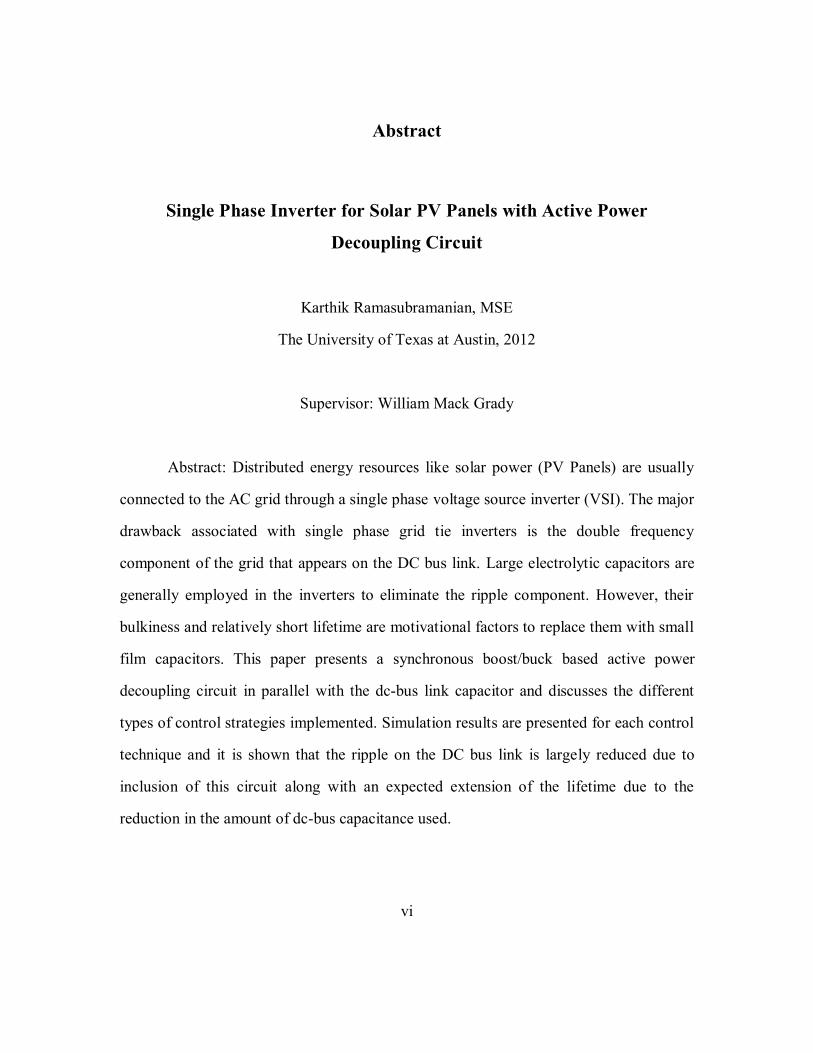
Abstract
Single Phase Inverter for Solar PV Panels with Active Power
Decoupling Circuit
Karthik Ramasubramanian, MSE
The University of Texas at Austin, 2012
Supervisor: William Mack Grady
Abstract: Distributed energy resources like solar power (PV Panels) are usually
connected to the AC grid through a single phase voltage source inverter (VSI). The major
drawback associated with single phase grid tie inverters is the double frequency
component of the grid that appears on the DC bus link. Large electrolytic capacitors are
generally employed in the inverters to eliminate the ripple component. However, their
bulkiness and relatively short lifetime are motivational factors to replace them with small
film capacitors. This paper presents a synchronous boost/buck based active power
decoupling circuit in parallel with the dc-bus link capacitor and discusses the different
types of control strategies implemented. Simulation results are presented for each control
technique and it is shown that the ripple on the DC bus link is largely reduced due to
inclusion of this circuit along with an expected extension of the lifetime due to the
reduction in the amount of dc-bus capacitance used.
vii
Table of Contents
Acknowledgements ............................................................................................. x
Abstract ............................................................................................................ vxi
List of Tables ...................................................................................................... x
List of Figures .................................................................................................. xxi
Chapter I: Overview of Grid Connected Photovoltaic Systems ............................ 1
The Bus Link Capacitor .............................................................................. 2
PV Inverters ............................................................................................... 5
Number of Power Processing Stages: ................................................. 6
Location of Power Decoupling Capacitors: ........................................ 7
Types of Grid Interfaces: .................................................................... 8
Final Schematic ........................................................................................ 10
Chapter II: Single Phase Power Pulsation ......................................................... 12
Chapter III: Methods Adopted to Resolve Single Phase Power Pulsation ........... 13
Existing Methods ...................................................................................... 13
Electrolytic Capacitor: ..................................................................... 13
Ceramic Capacitors: ......................................................................... 14
Thin Film Capacitors: ...................................................................... 14
Fluctuating DC Voltage Method: ..................................................... 14
Active Filtering: ............................................................................... 15
Notch Filter: ..................................................................................... 16
Flyback-Type Utility Interactive Inverter Circuit:............................. 17
Proposed Method ...................................................................................... 18
Active Power Decoupling: ............................................................... 18
Non-Isolated Topologies: ................................................................. 18
Isolated Topologies: ......................................................................... 20
Modes of Operation: ........................................................................ 22
viii
Chapter IV: Design of Power and Control Scheme-1 ......................................... 24
Power Circuit Design ................................................................................ 24
AC Side Inductor: ............................................................................ 24
DC Side Capacitor: .......................................................................... 27
Design of Control Loops for the Inverter .................................................. 27
Inner Current Loop: ......................................................................... 28
Selection of Gains for the PR Controller: ......................................... 29
Outer Voltage Loop: ........................................................................ 30
Selection of Gains for the Voltage Loop Controller: ......................... 31
Active Power Decoupling Circuit ............................................................. 33
Overall Control Scheme: .................................................................. 34
Chapter V: Design of Power and Control Scheme-2 .......................................... 35
Power Circuit Design ................................................................................ 35
AC Side Inductor: ............................................................................ 35
DC Side Capacitor: .......................................................................... 36
Design of Control Loops for the Inverter .................................................. 37
Inner Current Loop: ......................................................................... 37
Selection of Gains for the PI Controller: ........................................... 37
Outer Voltage Loop: ........................................................................ 38
Selection of Gains for the Voltage Loop Controller: ......................... 40
Active Power Decoupling Circuit ............................................................. 41
Overall Control Scheme: .................................................................. 41
Chapter VI: MATLAB Simulation Results .......................................................... 43
Control Scheme-1 ..................................................................................... 43
Scenario: .......................................................................................... 43
Inverter without Active Filter-Using Large Electrolytic Capacitor: ... 43
Inverter without Active Filter-Using Small Non-Electrolytic
Capacitor: ........................................................................................ 45
Inverter with Active Filter-Using Small Non-Electrolytic Capacitor: 48

ix
Control Scheme-2 ..................................................................................... 51
Scenario: .......................................................................................... 51
Inverter without Active Filter-Using Large Electrolytic Capacitor: ... 52
Inverter without Active Filter-Using Small Non-Electrolytic
Capacitor: ........................................................................................ 54
Inverter with Active Filter-Using Small Non-Electrolytic Capacitor: 56
Simulink Model ........................................................................................ 60
Chapter VII: Electronic Circuit Design and Simulation ..................................... 61
Inverter and Firing Circuit ........................................................................ 62
Voltage Control Scheme ........................................................................... 62
Multiplier Circuit ...................................................................................... 63
Current Feedback...................................................................................... 64
Current Control Scheme ........................................................................... 65
Feedforward Term .................................................................................... 65
Power Decoupling Circuit ......................................................................... 66
Simulation Results .................................................................................... 67
Scenario: .......................................................................................... 67
Inverter without Active Filter-Using Large Electrolytic Capacitor: ... 67
Inverter without Active Filter-Using Small Non-Electrolytic
Capacitor: ........................................................................................ 68
Inverter with Active Filter-Using Small Non-Electrolytic Capacitor: 69
Recommended Capacitors......................................................................... 70
Chapter VIII: Conclusions and Future Scope ..................................................... 73
Project Summary and Results ................................................................... 73
Future Scope ............................................................................................. 74
Bibliography ..................................................................................................... 75
x
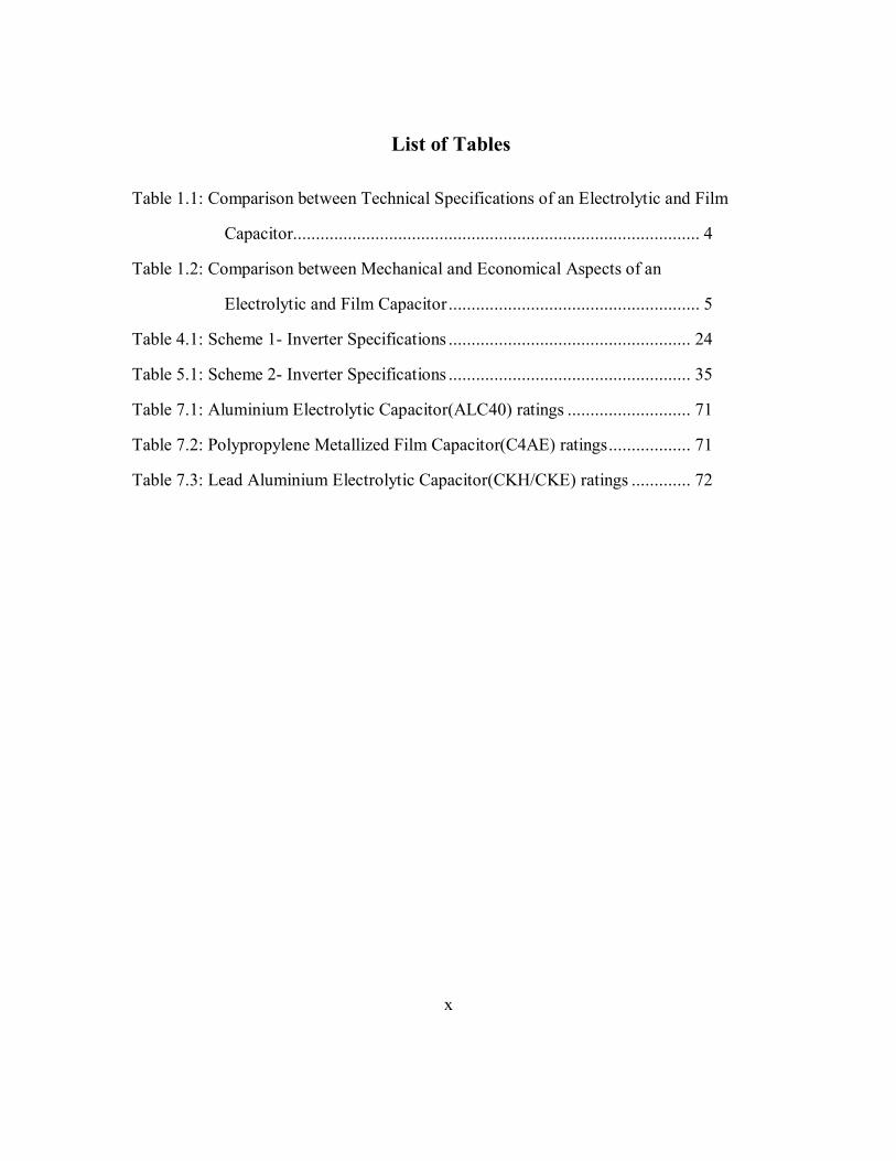
List of Tables
Table 1.1: Comparison between Technical Specifications of an Electrolytic and Film
Capacitor......................................................................................... 4
Table 1.2: Comparison between Mechanical and Economical Aspects of an
Electrolytic and Film Capacitor ....................................................... 5
Table 4.1: Scheme 1- Inverter Specifications ..................................................... 24
Table 5.1: Scheme 2- Inverter Specifications ..................................................... 35
Table 7.1: Aluminium Electrolytic Capacitor(ALC40) ratings ........................... 71
Table 7.2: Polypropylene Metallized Film Capacitor(C4AE) ratings .................. 71
Table 7.3: Lead Aluminium Electrolytic Capacitor(CKH/CKE) ratings ............. 72
xi
List of Figures
Fig.1.1: Two Stage Single Phase PV-Grid Interface. ............................................ 1
Fig.1.2: Single Phase Inverter .............................................................................. 2
Fig.1.3: Types of PV Inverters-a)A Single Power Processing Stage b) Dual Power
Processing Inverter c) Dual-Stage Inverter ...................................... 6
Fig.1.4: Different Locations of the Power Decoupling Capacitor ......................... 8
Fig.1.5: Grid-Connected Inverter Stages-a),b) Line-Commutated CSI Switching at
Twice the Line Frequency c),d) Self-Commutated Voltage Source
Inverter(VSI) Switching with High frequency in PWM or Hysteresis
Current Control ............................................................................... 9
Fig.1.6: Electrical Model of a PV Cell ............................................................... 11
Fig.1.7: Final Schematic of the PV-Grid Interface ............................................. 11
Fig.3.1: Large Electrolytic Capacitor Method .................................................... 13
Fig.3.2: Fluctuating DC Voltage Method ........................................................... 15
Fig.3.3: Circuit Diagram of the High Frequency Active Filtering Method .......... 16
Fig.3.4: Twin-Tee Notch Filter .......................................................................... 17
Fig.3.5: Flyback Inverter with High Power Decoupling ..................................... 17
Fig.3.6: Basic Topologies- a)Half-Bridge Converter b) Cuk Converter
c) SEPIC Converter ....................................................................... 19
Fig.3.7: Derived Topologies- a) Cascaded Half-Bridge Converter
b) Interleaved Half-Bridge Converter ............................................ 20
Fig.3.8: Isolated Topologies- a) One Voltage-Fed and One Current-Fed DC Side
b) Two Voltage-Fed DC Sides c) Two Current-Fed DC Sides ....... 21
Fig.3.9: PV-Grid Interface with Power Decoupling Circuit ................................ 22

xii
Fig.3.10: Graph of Instantaneous Power versus Mode of Operation ................... 23
Fig.3.11: Power Flow - a) Mode I of Operation b) Mode II of Operation ........... 23
Fig.4.1: Inverter Output Current Waveform ....................................................... 25
Fig.4.2: Scheme 1- FFT Analysis of the Inverter Output .................................... 26
Fig.4.3: Scheme 1- Inner Current Loop.............................................................. 28
Fig.4.4: Scheme 1- Bode Plot of Inner Current Loop ......................................... 30
Fig.4.5: Scheme 1- Outer Voltage Loop ............................................................ 31
Fig.4.6: Scheme 1- Bode Plot of Outer Voltage Loop ........................................ 33
Fig.4.7: Scheme 1- Auxiliary Converter Control Implementation ...................... 34
Fig.4.8: Overall Control Scheme-1 .................................................................... 34
Fig.5.1: Scheme 2- FFT Analysis of the Inverter Output .................................... 36
Fig.5.2: Scheme 2- Inner Current Loop.............................................................. 37
Fig.5.3: Scheme 2- Bode Plot of Inner Current Loop ......................................... 38
Fig.5.4: Scheme 2- Outer Voltage Loop ............................................................ 39
Fig.5.5: Scheme 2- Bode Plot of Outer Voltage Loop ........................................ 40
Fig.5.6: Overall Control Scheme-2 .................................................................... 42
Fig.6.1: Scheme 1 & Scenario 1- DC Bus Link Capacitor Voltage ..................... 43
Fig.6.2: Scheme 1 & Scenario 1- Grid Current Superimposed on Grid Voltage.. 44
Fig.6.3: Scheme 1 & Scenario 1- Inverter Output Voltage ................................. 44
Fig.6.4: Scheme 1 & Scenario 1- Inverter Input Current .................................... 45
Fig.6.5: Scheme 1 & Scenario 2- DC Bus Link Capacitor Voltage ..................... 46
Fig.6.6: Scheme 1 & Scenario 2- Grid Current Superimposed on Grid Voltage.. 46
Fig.6.7: Scheme 1 & Scenario 2- Inverter Output Voltage ................................. 47
Fig.6.8: Scheme 1 & Scenario 2- Inverter Input Current .................................... 47
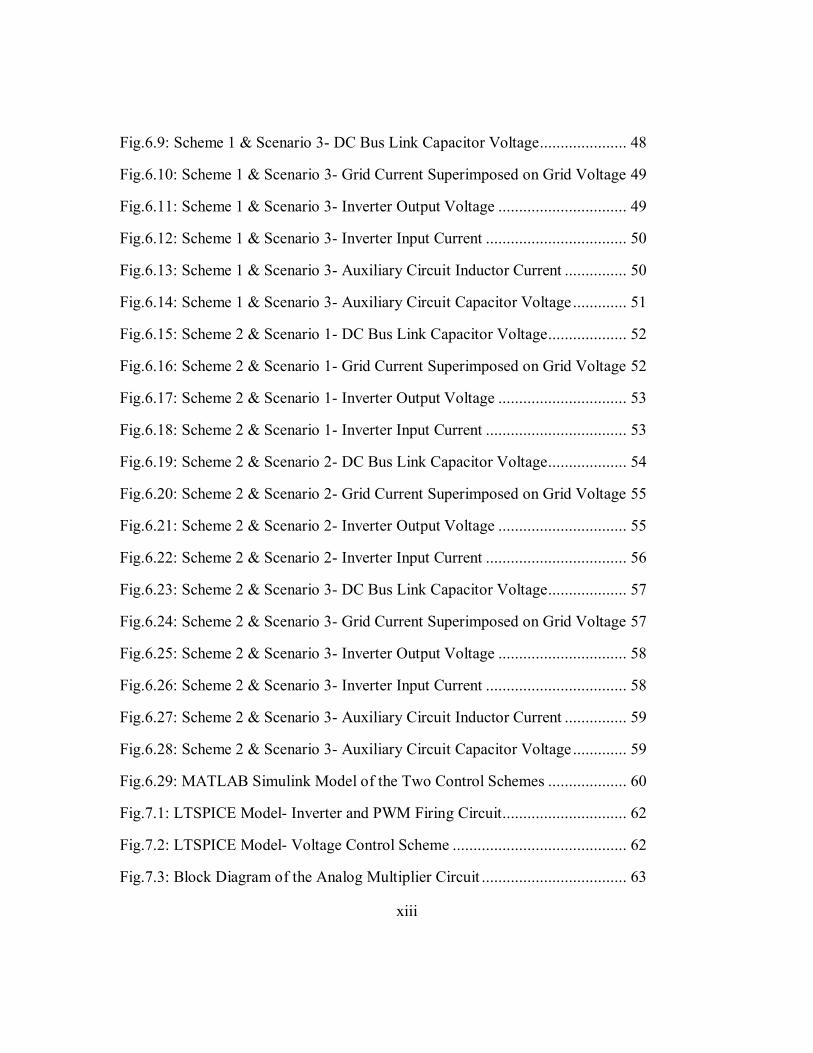
xiii
Fig.6.9: Scheme 1 & Scenario 3- DC Bus Link Capacitor Voltage ..................... 48
Fig.6.10: Scheme 1 & Scenario 3- Grid Current Superimposed on Grid Voltage 49
Fig.6.11: Scheme 1 & Scenario 3- Inverter Output Voltage ............................... 49
Fig.6.12: Scheme 1 & Scenario 3- Inverter Input Current .................................. 50
Fig.6.13: Scheme 1 & Scenario 3- Auxiliary Circuit Inductor Current ............... 50
Fig.6.14: Scheme 1 & Scenario 3- Auxiliary Circuit Capacitor Voltage ............. 51
Fig.6.15: Scheme 2 & Scenario 1- DC Bus Link Capacitor Voltage ................... 52
Fig.6.16: Scheme 2 & Scenario 1- Grid Current Superimposed on Grid Voltage 52
Fig.6.17: Scheme 2 & Scenario 1- Inverter Output Voltage ............................... 53
Fig.6.18: Scheme 2 & Scenario 1- Inverter Input Current .................................. 53
Fig.6.19: Scheme 2 & Scenario 2- DC Bus Link Capacitor Voltage ................... 54
Fig.6.20: Scheme 2 & Scenario 2- Grid Current Superimposed on Grid Voltage 55
Fig.6.21: Scheme 2 & Scenario 2- Inverter Output Voltage ............................... 55
Fig.6.22: Scheme 2 & Scenario 2- Inverter Input Current .................................. 56
Fig.6.23: Scheme 2 & Scenario 3- DC Bus Link Capacitor Voltage ................... 57
Fig.6.24: Scheme 2 & Scenario 3- Grid Current Superimposed on Grid Voltage 57
Fig.6.25: Scheme 2 & Scenario 3- Inverter Output Voltage ............................... 58
Fig.6.26: Scheme 2 & Scenario 3- Inverter Input Current .................................. 58
Fig.6.27: Scheme 2 & Scenario 3- Auxiliary Circuit Inductor Current ............... 59
Fig.6.28: Scheme 2 & Scenario 3- Auxiliary Circuit Capacitor Voltage ............. 59
Fig.6.29: MATLAB Simulink Model of the Two Control Schemes ................... 60
Fig.7.1: LTSPICE Model- Inverter and PWM Firing Circuit.............................. 62
Fig.7.2: LTSPICE Model- Voltage Control Scheme .......................................... 62
Fig.7.3: Block Diagram of the Analog Multiplier Circuit ................................... 63
xiv
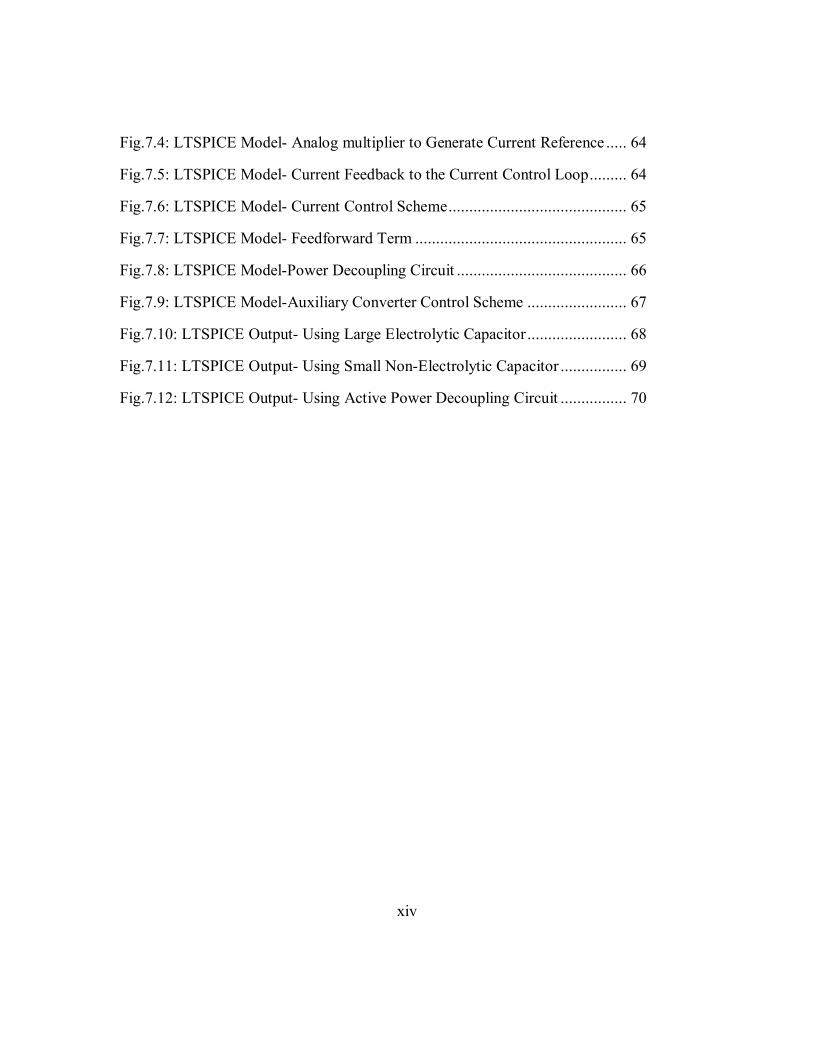
Fig.7.4: LTSPICE Model- Analog multiplier to Generate Current Reference ..... 64
Fig.7.5: LTSPICE Model- Current Feedback to the Current Control Loop ......... 64
Fig.7.6: LTSPICE Model- Current Control Scheme ........................................... 65
Fig.7.7: LTSPICE Model- Feedforward Term ................................................... 65
Fig.7.8: LTSPICE Model-Power Decoupling Circuit ......................................... 66
Fig.7.9: LTSPICE Model-Auxiliary Converter Control Scheme ........................ 67
Fig.7.10: LTSPICE Output- Using Large Electrolytic Capacitor ........................ 68
Fig.7.11: LTSPICE Output- Using Small Non-Electrolytic Capacitor ................ 69
Fig.7.12: LTSPICE Output- Using Active Power Decoupling Circuit ................ 70
1
Chapter I: Overview of Grid Connected Photovoltaic Systems
In recent times, there has been an increasing interest in renewable energy among
power electronics authorities in response to increased concern for the environment.
Various types of inverter circuits and their control schemes for photovoltaic (PV) power
generation systems have been studied. Especially, in the area of PV power generation
system for residential purposes, small power single phase utility interactive inverters have
been used continually [1]-[5].
Inverters interfacing the PV module(s) with the grid have two major tasks:
Ensure that the PV module(s) operate at the maximum power point (MPP)
Inject a sinusoidal current into the grid.
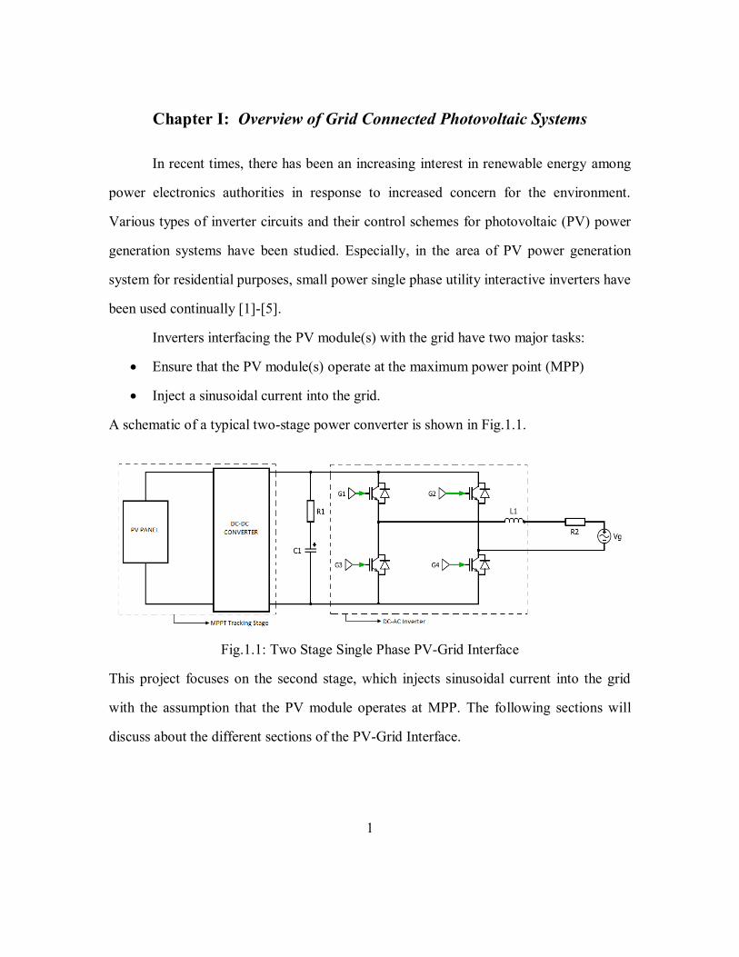
A schematic of a typical two-stage power converter is shown in Fig.1.1.
Fig.1.1: Two Stage Single Phase PV-Grid Interface
This project focuses on the second stage, which injects sinusoidal current into the grid
with the assumption that the PV module operates at MPP. The following sections will
discuss about the different sections of the PV-Grid Interface.
2
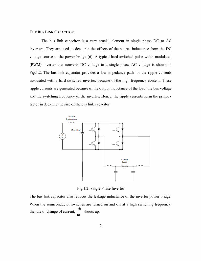
THE BUS LINK CAPACITOR
The bus link capacitor is a very crucial element in single phase DC to AC
inverters. They are used to decouple the effects of the source inductance from the DC
voltage source to the power bridge [6]. A typical hard switched pulse width modulated
(PWM) inverter that converts DC voltage to a single phase AC voltage is shown in
Fig.1.2. The bus link capacitor provides a low impedance path for the ripple currents
associated with a hard switched inverter, because of the high frequency content. These
ripple currents are generated because of the output inductance of the load, the bus voltage
and the switching frequency of the inverter. Hence, the ripple currents form the primary
factor in deciding the size of the bus link capacitor.
Fig.1.2: Single Phase Inverter
The bus link capacitor also reduces the leakage inductance of the inverter power bridge.
When the semiconductor switches are turned on and off at a high switching frequency,
the rate of change of current, di
dt shoots up.

3
As a result of this shoot up, voltage spikes are produced according to the relation
L
diV L
dt (1.1)
where,
L is the leakage inductance
VL is the voltage across the leakage inductance
This effect of the leakage inductance leads to decrease in the efficiency of the inverter
power bridge. If the leakage inductance gets too large, the switching frequency of the
power switches must be decreased to prevent the voltage spikes from damaging the
power devices, and decreasing the switching frequency decreases the turn on and turn off
losses in each of the power switches contributing to lower switching losses which
manifest themselves in lesser heat dissipation in the switching devices. Thus, a low
impedance DC bus is essential for an efficient inverter design. The bus link capacitor’s
equivalent series inductance (ESL) and external packaging is also, a key to reducing
leakage inductance in the inverter power bridge.
Different types of capacitors maybe used including:
Electrolytic Capacitors
Film Capacitors
Ceramic capacitors
The succeeding chapters will discuss the disadvantages and advantages of using the
above mentioned types of capacitors. Table 1.1 and Table 1.2 compares the technical,
mechanical and economical aspects of an Aluminium electrolytic capacitor and a dry
Propylene film capacitor.

4
Parameter Electrolytic Capacitor(Al) Film Capacitor(Dry
Propylene)
Temperature range -250C to 105
0C -55
0C to 105
0C
Capacitance 5600μF±20% 350μF±10%
Capacitor Working Voltage 450V DC 500V DC
Capacitor Surge Voltage 500V DC 650V DC
ESR at 10kHz (mΩ) 20 typical 0.8-1 typical
ESL <27nH
Leakage Current (μA) 4.76 at 450V DC 0.035 at 500V DC
Ripple Current(450C)
Ambient 10kHz (Arms)
35.64 78.10
Power Density Ambient
10kHz, 450C (W/in
3)
303.3
1486.5
Current Density Ambient
10kHz,450C(Arms/in
3)
0.67 2.97
Dissipated Heating Loss(W) 16.5 0.83
Thermal
Resistance(0C/Wdissipated)
4.7
Energy Density Ambient
10kHz,450C(J/in
3)
10.7 1.7
Table 1.1: Comparison between Technical Specifications of an Electrolytic and Film
Capacitor
5
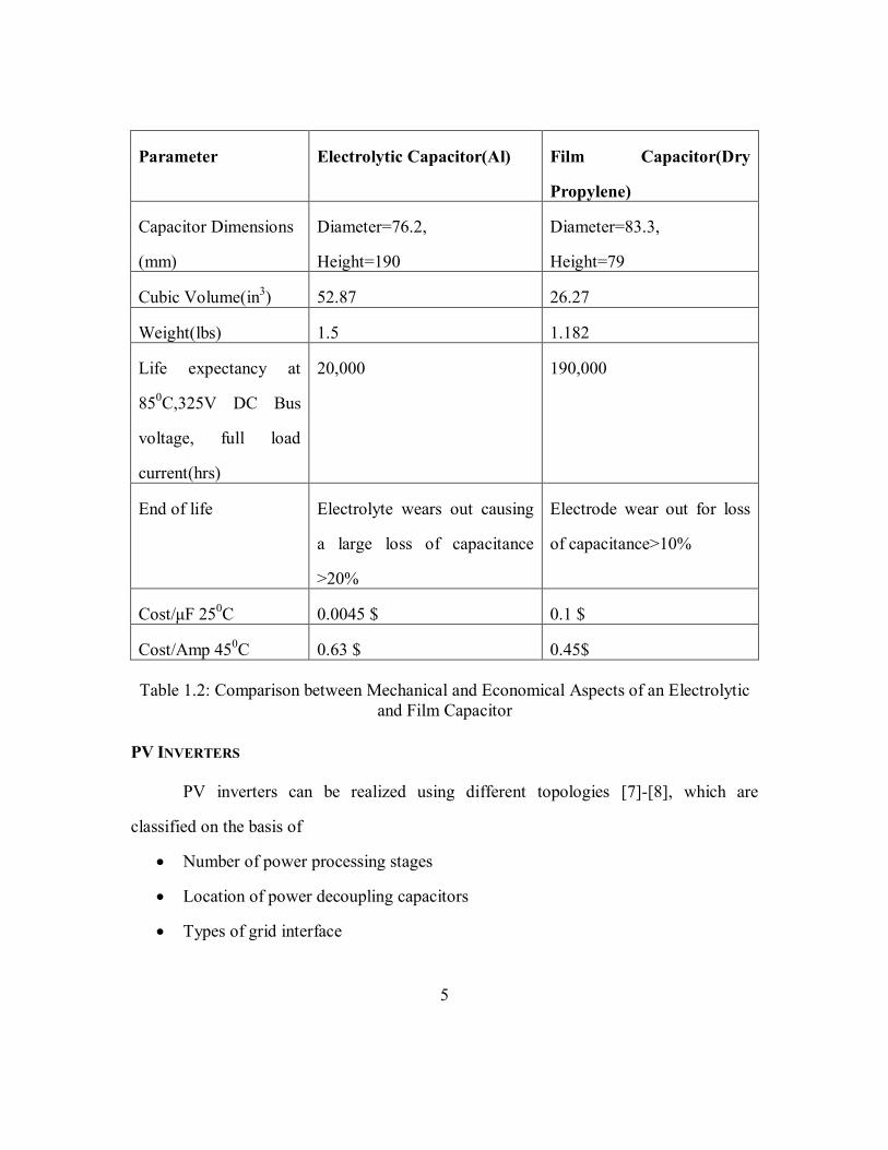
Parameter Electrolytic Capacitor(Al) Film Capacitor(Dry
Propylene)
Capacitor Dimensions
(mm)
Diameter=76.2,
Height=190
Diameter=83.3,
Height=79
Cubic Volume(in3) 52.87
26.27
Weight(lbs) 1.5 1.182
Life expectancy at
850C,325V DC Bus
voltage, full load
current(hrs)
20,000 190,000
End of life Electrolyte wears out causing
a large loss of capacitance
>20%
Electrode wear out for loss
of capacitance>10%
Cost/μF 250C 0.0045 $ 0.1 $
Cost/Amp 450C 0.63 $ 0.45$
Table 1.2: Comparison between Mechanical and Economical Aspects of an Electrolytic
and Film Capacitor
PV INVERTERS
PV inverters can be realized using different topologies [7]-[8], which are
classified on the basis of
Number of power processing stages
Location of power decoupling capacitors
Types of grid interface
6
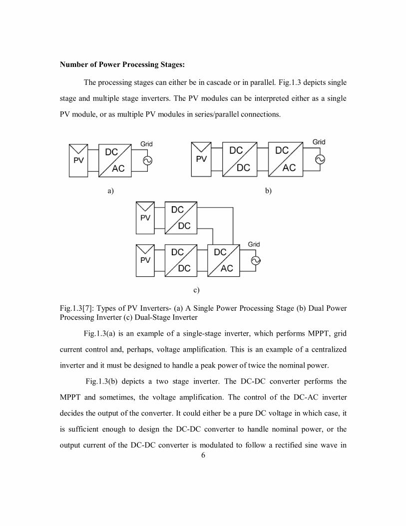
Number of Power Processing Stages:
The processing stages can either be in cascade or in parallel. Fig.1.3 depicts single
stage and multiple stage inverters. The PV modules can be interpreted either as a single
PV module, or as multiple PV modules in series/parallel connections.
a) b)
c)
Fig.1.3[7]: Types of PV Inverters- (a) A Single Power Processing Stage (b) Dual Power
Processing Inverter (c) Dual-Stage Inverter
Fig.1.3(a) is an example of a single-stage inverter, which performs MPPT, grid
current control and, perhaps, voltage amplification. This is an example of a centralized
inverter and it must be designed to handle a peak power of twice the nominal power.
Fig.1.3(b) depicts a two stage inverter. The DC-DC converter performs the
MPPT and sometimes, the voltage amplification. The control of the DC-AC inverter
decides the output of the converter. It could either be a pure DC voltage in which case, it
is sufficient enough to design the DC-DC converter to handle nominal power, or the
output current of the DC-DC converter is modulated to follow a rectified sine wave in

7
which case, the converter needs to be designed to handle twice the nominal power. The
DC-AC inverter controls the grid current by means of PWM or hysteresis current control
in the former solution. In the latter, the inverter switches at line frequency, and converts
the rectified current to a full-wave sine. The converter takes care of the current control.
For low nominal power, the latter solution is recommended for higher efficiency, whereas
in the case of high nominal power the PWM mode is recommended.
Finally, Fig.1.3(c) is the solution for multi-string inverter. The sole task for each
DC-DC converter is MPPT and perhaps voltage amplification. The converters are
connected to the DC link of an inverter, which takes care of the grid current control. This
solution is recommended since better control of each PV module/string is achieved and
that inverter may be based on standard variable speed drives. In this project, the inverter
topology chosen can be considered to be either a single stage inverter or a two stage
inverter, since the focus is on controlling the grid current and DC bus link voltage, and
the PV module is assumed to be operating at MPP.
Location of Power Decoupling Capacitors:
Power decoupling can be obtained either by using an electrolytic capacitor or a film
capacitor. The capacitor is either placed in parallel with the PV modules for a single stage
inverter as shown in Fig.1.4a) or in the DC link between the inverter stages, for a multi-
stage inverter as shown in Fig.1.4b). In this project, the decoupling capacitor is placed in
parallel with the PV modules.

8
a) b)
Fig.1.4[7] : Different Locations of the Power Decoupling Capacitor.
Types of Grid Interfaces:
Current source inverters are the main priority in this classification since, injecting
a sinusoidal current into the grid is our prime concern. Four kinds of grid-connected
inverters are shown in Fig.1.5. The topologies of Fig. 1.5(a) and 1.5(b) are line-
frequency-commutated current-source inverters (CSIs). The current into the stage is
already modulated to follow a rectified sinusoidal waveform and the task for the circuit is
simply to re-create the sine wave and inject it into the grid. The circuits apply zero-
voltage switching (ZVS) and zero-current switching (ZCS), and hence switching losses
are absent. Since the current is modulated by another stage, the other stage must be
designed for a peak power of twice the nominal power, and power decoupling must be
achieved with a capacitor in parallel with the PV module(s). The converter feeding the
circuit of Fig.1.5(a) can be a push–pull with a single secondary transformer winding, and
a flyback with two secondary windings for the circuit of Fig.1.5(b).
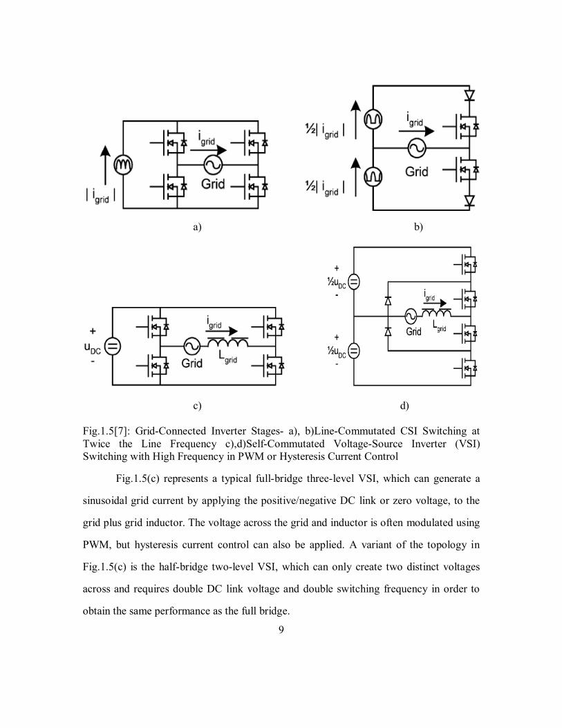
9
a) b)
c) d)
Fig.1.5[7]: Grid-Connected Inverter Stages- a), b)Line-Commutated CSI Switching at
Twice the Line Frequency c),d)Self-Commutated Voltage-Source Inverter (VSI)
Switching with High Frequency in PWM or Hysteresis Current Control
Fig.1.5(c) represents a typical full-bridge three-level VSI, which can generate a
sinusoidal grid current by applying the positive/negative DC link or zero voltage, to the
grid plus grid inductor. The voltage across the grid and inductor is often modulated using
PWM, but hysteresis current control can also be applied. A variant of the topology in
Fig.1.5(c) is the half-bridge two-level VSI, which can only create two distinct voltages
across and requires double DC link voltage and double switching frequency in order to
obtain the same performance as the full bridge.
10
Fig.1.5(d) represents a half-bridge diode clamped three-level VSI, which is one of
many different multilevel VSIs, which can create 3, 5, 7 distinct voltages across the grid
and inductor. This is beneficial since the switching frequency of each transistor can be
reduced and, which gives rise to lower losses. The command signals for the transistors in
the CSI and the reference for the grid-current waveform are mostly based on measured
grid voltage or zero-crossing detection. This may result in severe problems with power
quality and unnecessary fault situations. The main reasons for these problems are the
background (voltage) harmonics and poor design. The harmonics may initiate series
resonance with the capacitors placed around in the grid, due to positive feedback of the
inverter current or a noisy signal from the zero-crossing detection. A solution for this
problem is to use a phase-locked loop (PLL) for establishing a current waveform
reference of high quality.
In this project, the full bridge three-level VSI is chosen as the grid interface.
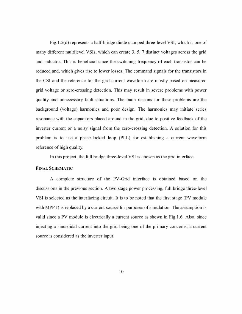
FINAL SCHEMATIC
A complete structure of the PV-Grid interface is obtained based on the
discussions in the previous section. A two stage power processing, full bridge three-level
VSI is selected as the interfacing circuit. It is to be noted that the first stage (PV module
with MPPT) is replaced by a current source for purposes of simulation. The assumption is
valid since a PV module is electrically a current source as shown in Fig.1.6. Also, since
injecting a sinusoidal current into the grid being one of the primary concerns, a current
source is considered as the inverter input.
11
Fig.1.6: Simplified Electrical Model of a PV Cell
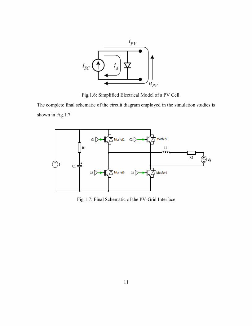
The complete final schematic of the circuit diagram employed in the simulation studies is
shown in Fig.1.7.
Fig.1.7: Final Schematic of the PV-Grid Interface

12
Chapter II: Single Phase Power Pulsation
Consider the schematic of the grid connected PV system shown in Fig.1.7.
Assuming unity power factor operation and neglecting the energy stored in the inductor,
the instantaneous power flowing through the inverter can be determined as follows [9].
2 sin( )gV V t (2.1)
2 sin( )gI I t (2.2)
2sin ( ) cos(2 ) (1 cos(2 ))inv g g g g g gP V I t V I V I t P t (2.3)
where,
gV is the peak value of the grid voltage
gI is the peak value of the grid current
P is the average value of the active power injected into the grid
We can also observe that,
cos(2 )capacitor invP P P P t (2.4)
Thus the difference between the average and the instantaneous power in the ac side of the
inverter produces a voltage ripple at twice the line frequency on the DC bus link
capacitor. This is one of the primary problems faced and the methods adopted for
resolving this issue is addressed in the upcoming chapters.
13
Chapter III: Methods Adopted to Resolve Single Phase Power Pulsation
A number of methods have been proposed in literature to tackle the problem of
the double frequency component of the grid on the DC bus link. Some of them are
explained in the following paragraphs.
EXISTING METHODS
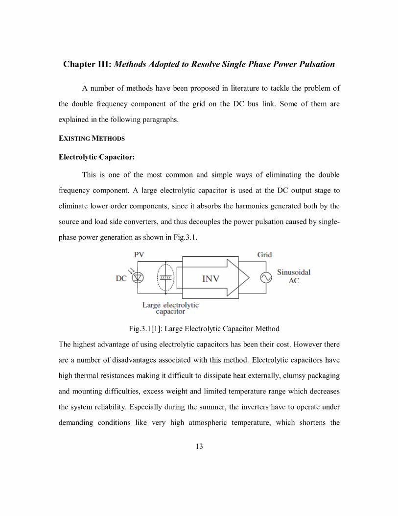
Electrolytic Capacitor:
This is one of the most common and simple ways of eliminating the double
frequency component. A large electrolytic capacitor is used at the DC output stage to
eliminate lower order components, since it absorbs the harmonics generated both by the
source and load side converters, and thus decouples the power pulsation caused by single-
phase power generation as shown in Fig.3.1.
Fig.3.1[1]: Large Electrolytic Capacitor Method
The highest advantage of using electrolytic capacitors has been their cost. However there
are a number of disadvantages associated with this method. Electrolytic capacitors have
high thermal resistances making it difficult to dissipate heat externally, clumsy packaging
and mounting difficulties, excess weight and limited temperature range which decreases
the system reliability. Especially during the summer, the inverters have to operate under
demanding conditions like very high atmospheric temperature, which shortens the
14
lifetime of the inverter, since the life of the electrolytic capacitor reduces when used
under high temperature. They also suffer from low ripple current capability due to high
ESR and ESL and hence they need to be sized for a much higher value than required for
the inverter operation. Using large capacitors has its own associated problems such as
requirement of a bleed-resistor or discharge circuit to discharge large capacitors on
system shutdown.
Ceramic Capacitors:
Ceramic capacitors are an example of passive capacitor filter. They are beneficial
from the perspective of increased reliability and being less lossy when compared to
electrolytic capacitors due to lower values of ESR. However, they are less preferred due
to their large physical size and weight. They also ring with filter inductance along with
the injected harmonic current.
Thin Film Capacitors:
Thin film capacitors can be used in the place of electrolytic capacitors. High
performance inverters used in electric vehicles and aircraft to name a few are now turning
to film capacitors because they do not have the limitations of electrolytic capacitors and
have high ripple current capability. The only disadvantage of film capacitors is that of the
increased cost per μF and thus provides a very expensive solution.
Fluctuating DC Voltage Method:
This method involves designing a converter which can withstand a larger voltage ripple
on the DC bus link, around 25%, rather than 5% [10]. The block diagram of this method
is shown in Fig.3.2.

15
Fig.3.2 [10]: Fluctuating DC Voltage Method
Increasing the voltage ripple on the DC bus link reduces the size of the capacitor that
needs to be designed accordingly. The capacitor designed for the increased ripple
condition (25%) on the DC link is 500 times smaller than the capacitor used for the lower
ripple condition (5%) which is a stronger DC link. However, the drawback of this method
is the slower response of the voltage control loop making the DC bus voltage susceptible
to large variations due to sudden active power variations in the system. The bandwidth of
the voltage control loop is restricted to only 10Hz.
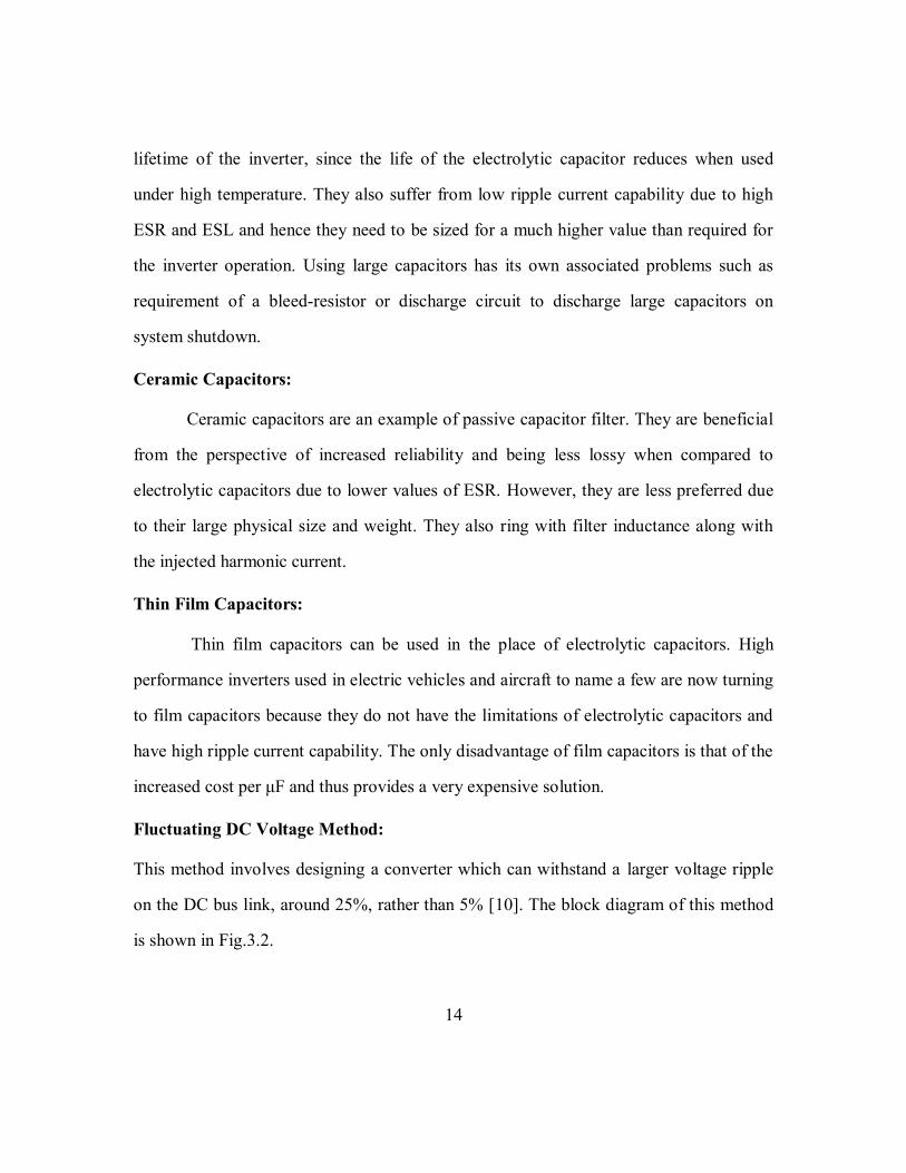
Active Filtering:
A high frequency current-fed type active filter is used instead of the electrolytic
capacitor on the DC link of the inverter [11]-[14]. Fig.3.3 depicts the circuitry used in the
method. The filter absorbs the harmonic currents generated by the rectifier and the
inverter thereby smoothening the DC voltage. The components in the active filter have
high reliability and less size and cost compared to an equivalent ac capacitor. The active
filter eliminates unnecessary resonance effect in the DC link, and filtering function is
programmable providing flexibility of operation.
16
Fig.3.3: Circuit Configuration of the High Frequency Active Filtering Method
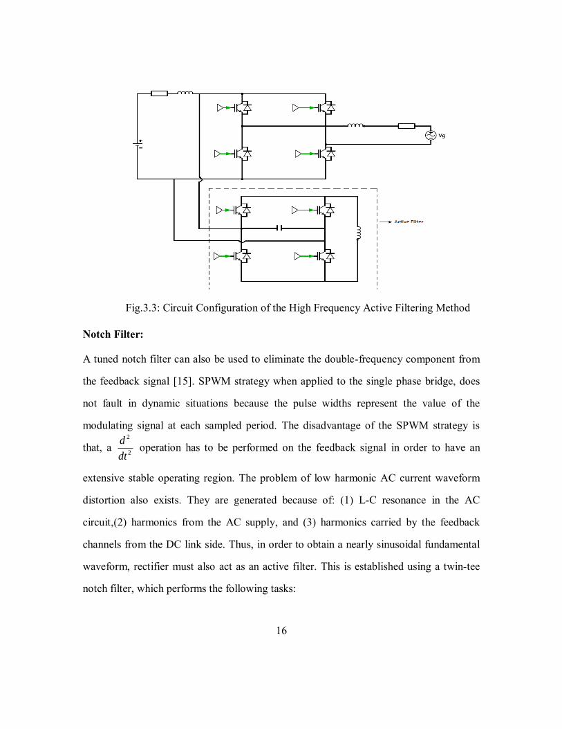
Notch Filter:
A tuned notch filter can also be used to eliminate the double-frequency component from
the feedback signal [15]. SPWM strategy when applied to the single phase bridge, does
not fault in dynamic situations because the pulse widths represent the value of the
modulating signal at each sampled period. The disadvantage of the SPWM strategy is
that, a 2
2
d
dt operation has to be performed on the feedback signal in order to have an
extensive stable operating region. The problem of low harmonic AC current waveform
distortion also exists. They are generated because of: (1) L-C resonance in the AC
circuit,(2) harmonics from the AC supply, and (3) harmonics carried by the feedback
channels from the DC link side. Thus, in order to obtain a nearly sinusoidal fundamental
waveform, rectifier must also act as an active filter. This is established using a twin-tee
notch filter, which performs the following tasks:
17
Active filtering to remove the low-order harmonics on the ac side
Achieving an extensive stable domain without implementing the 2
2
d
dt operation
The circuit diagram of a twin tee notch filter is shown in Fig.3.4.
Fig.3.4: Twin Tee Notch Filter
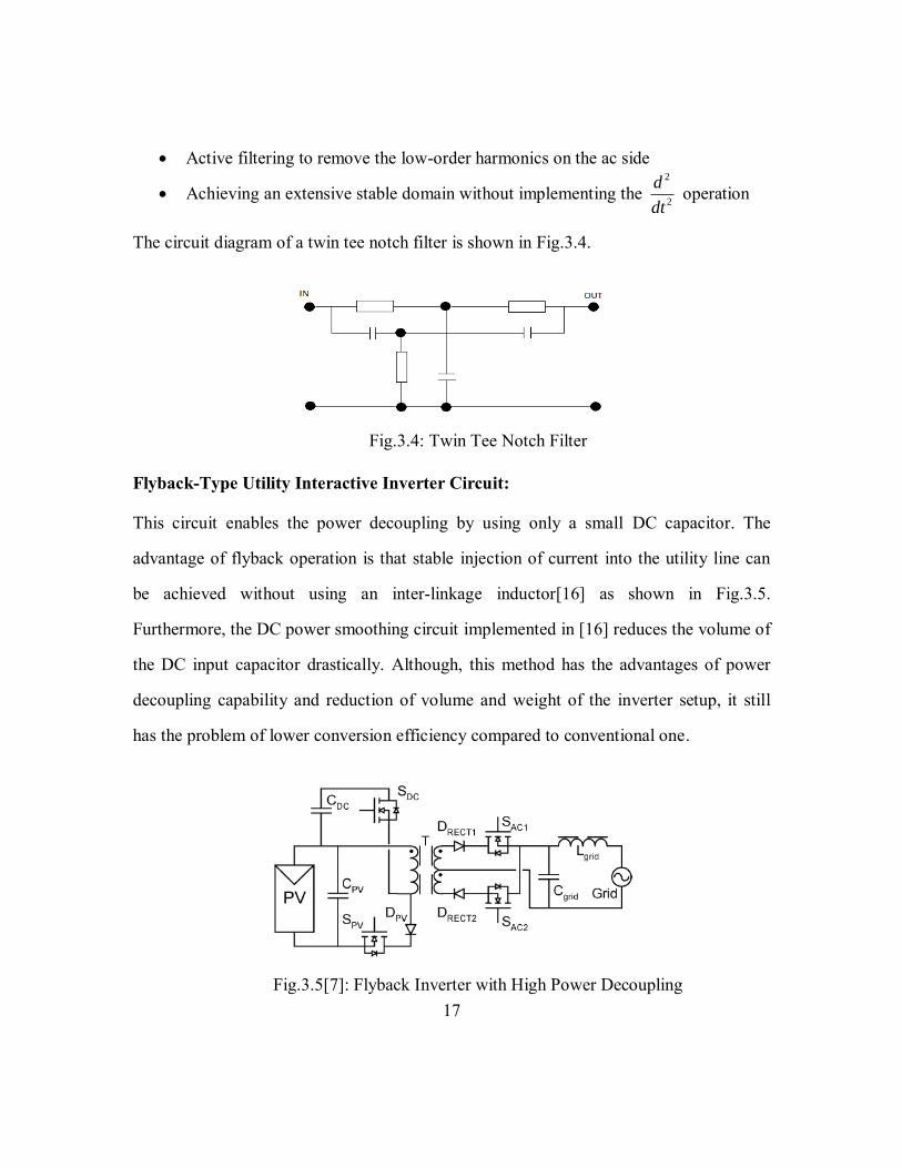
Flyback-Type Utility Interactive Inverter Circuit:
This circuit enables the power decoupling by using only a small DC capacitor. The
advantage of flyback operation is that stable injection of current into the utility line can
be achieved without using an inter-linkage inductor[16] as shown in Fig.3.5.
Furthermore, the DC power smoothing circuit implemented in [16] reduces the volume of
the DC input capacitor drastically. Although, this method has the advantages of power
decoupling capability and reduction of volume and weight of the inverter setup, it still
has the problem of lower conversion efficiency compared to conventional one.
Fig.3.5[7]: Flyback Inverter with High Power Decoupling
18
PROPOSED METHOD
In this project an active power decoupling circuit is proposed as a suitable
solution. The following sub-sections will elaborate on the same.
Active Power Decoupling:
The need for the active power decoupling circuit arises, to account for the large
excursions in the DC bus voltage ripple when the active power supplied by the first stage
to the DC bus changes. Inherently, it increases the bandwidth of operation. Since the
power decoupling circuit is independent of the inverter portion, there is no limitation on
decoupling capacitor voltage. The objective of the decoupling circuit is to shift the energy
of the 120Hz ripple stored in the DC link capacitor to an auxiliary storage capacitor. This
could also, be viewed as the auxiliary converter circuit injecting an equal and opposite
current to the 120Hz ripple observed at the output of the dc link capacitor. This is
realized using a bidirectional DC-DC converter typically used for energy storage. During
charging mode, the ratio of output to input voltage is lower than ‘1’ and during
discharging mode the ratio of output to input voltage is greater than ‘1’.The bidirectional
converters can either be having an isolated or a non-isolated topology. The performance
comparison of different configurations in both the topologies will be explained in the
next section.
Non-Isolated Topologies:
Non-isolated bi-directional DC-DC converters have the following advantages:
Simple implementation and Low Cost
High Efficiency
High reliability

19
These converters can be classified into two types [17-[18]:
Basic Topologies –
Half-Bridge Converter
Cuk Converter
SEPIC Converter
Derived Topologies –
Cascaded Half-Bridge Converter
Interleaved Half-Bridge Converter
a) b)
c)
Fig.3.6[17]: Basic Topologies-a) Half-Bridge Converter b) Cuk Converter c) SEPIC
Converter
Fig.3.6a) shows the Half-bridge converter, one of the widely used topologies. The
converter operates either in Buck or in Boost mode.Fig.3.6b) and Fig.3.6c) shows the
Cuk and SEPIC converter respectively which convert power bi-directionally by using two
active switches. In all the basic topologies, the battery is connected to C1 through a
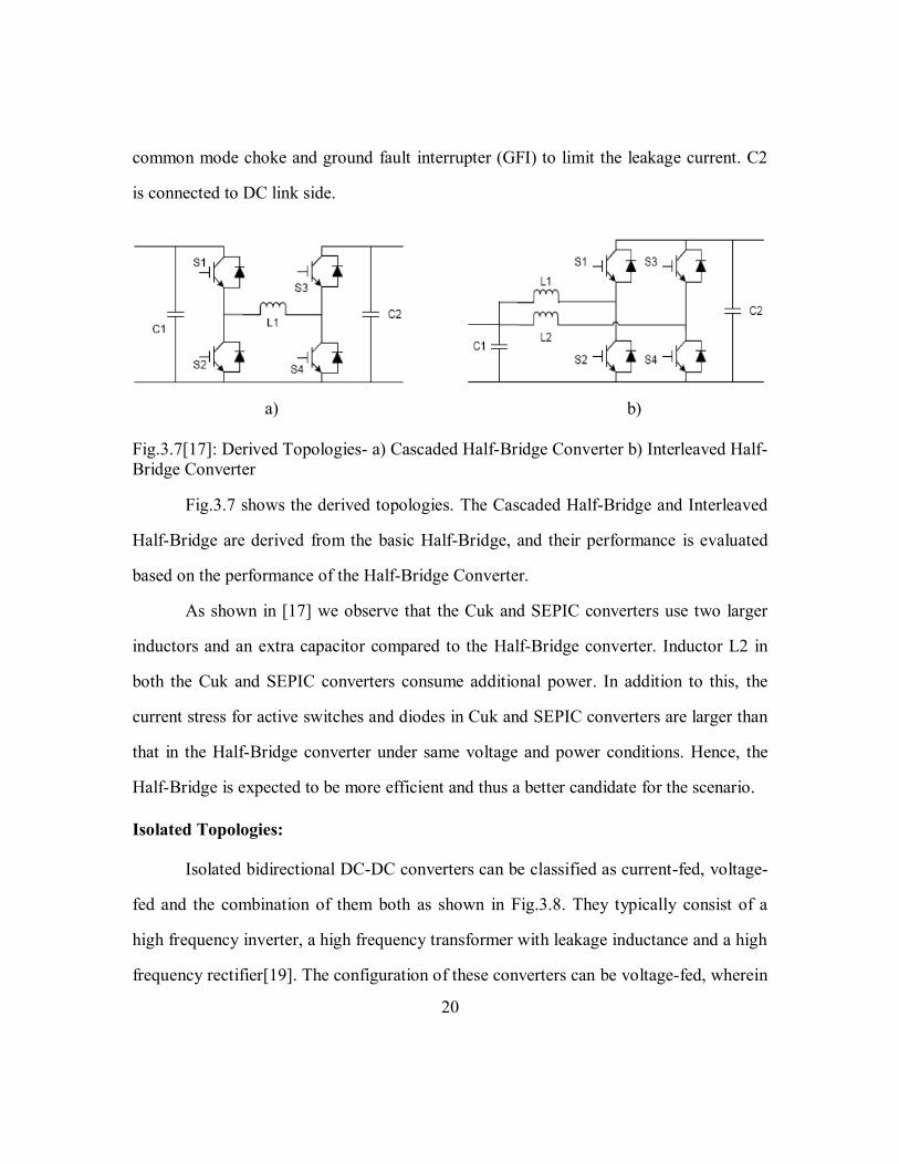
20
common mode choke and ground fault interrupter (GFI) to limit the leakage current. C2
is connected to DC link side.
a) b)
Fig.3.7[17]: Derived Topologies- a) Cascaded Half-Bridge Converter b) Interleaved Half-
Bridge Converter
Fig.3.7 shows the derived topologies. The Cascaded Half-Bridge and Interleaved
Half-Bridge are derived from the basic Half-Bridge, and their performance is evaluated
based on the performance of the Half-Bridge Converter.
As shown in [17] we observe that the Cuk and SEPIC converters use two larger
inductors and an extra capacitor compared to the Half-Bridge converter. Inductor L2 in
both the Cuk and SEPIC converters consume additional power. In addition to this, the
current stress for active switches and diodes in Cuk and SEPIC converters are larger than
that in the Half-Bridge converter under same voltage and power conditions. Hence, the
Half-Bridge is expected to be more efficient and thus a better candidate for the scenario.
Isolated Topologies:
Isolated bidirectional DC-DC converters can be classified as current-fed, voltage-
fed and the combination of them both as shown in Fig.3.8. They typically consist of a
high frequency inverter, a high frequency transformer with leakage inductance and a high
frequency rectifier[19]. The configuration of these converters can be voltage-fed, wherein
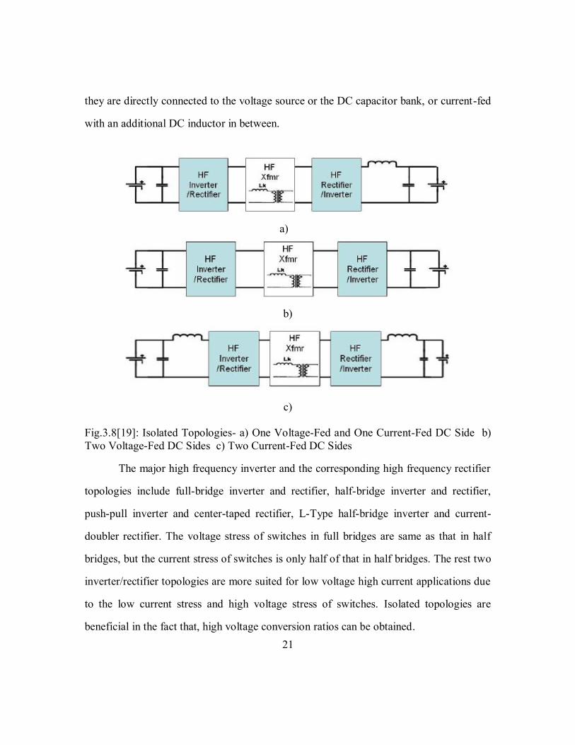
21
they are directly connected to the voltage source or the DC capacitor bank, or current-fed
with an additional DC inductor in between.
a)
b)
c)
Fig.3.8[19]: Isolated Topologies- a) One Voltage-Fed and One Current-Fed DC Side b)
Two Voltage-Fed DC Sides c) Two Current-Fed DC Sides
The major high frequency inverter and the corresponding high frequency rectifier
topologies include full-bridge inverter and rectifier, half-bridge inverter and rectifier,
push-pull inverter and center-taped rectifier, L-Type half-bridge inverter and current-
doubler rectifier. The voltage stress of switches in full bridges are same as that in half
bridges, but the current stress of switches is only half of that in half bridges. The rest two
inverter/rectifier topologies are more suited for low voltage high current applications due
to the low current stress and high voltage stress of switches. Isolated topologies are
beneficial in the fact that, high voltage conversion ratios can be obtained.

22
The main drawback of isolated topologies is the leakage flux, due to the presence
of transformers which results in reduced efficiency [20]. In addition to this, there is an
increase in the number of components used resulting in increased cost and size.
In this project the auxiliary converter has the configuration of the Half-Bridge
topology, for energy storage. The complete schematic of the PV-Grid Interface including
the power decoupling circuit is shown in Fig.3.9.
Fig.3.9: PV-Grid Interface with Power Decoupling Circuit
Modes of Operation:
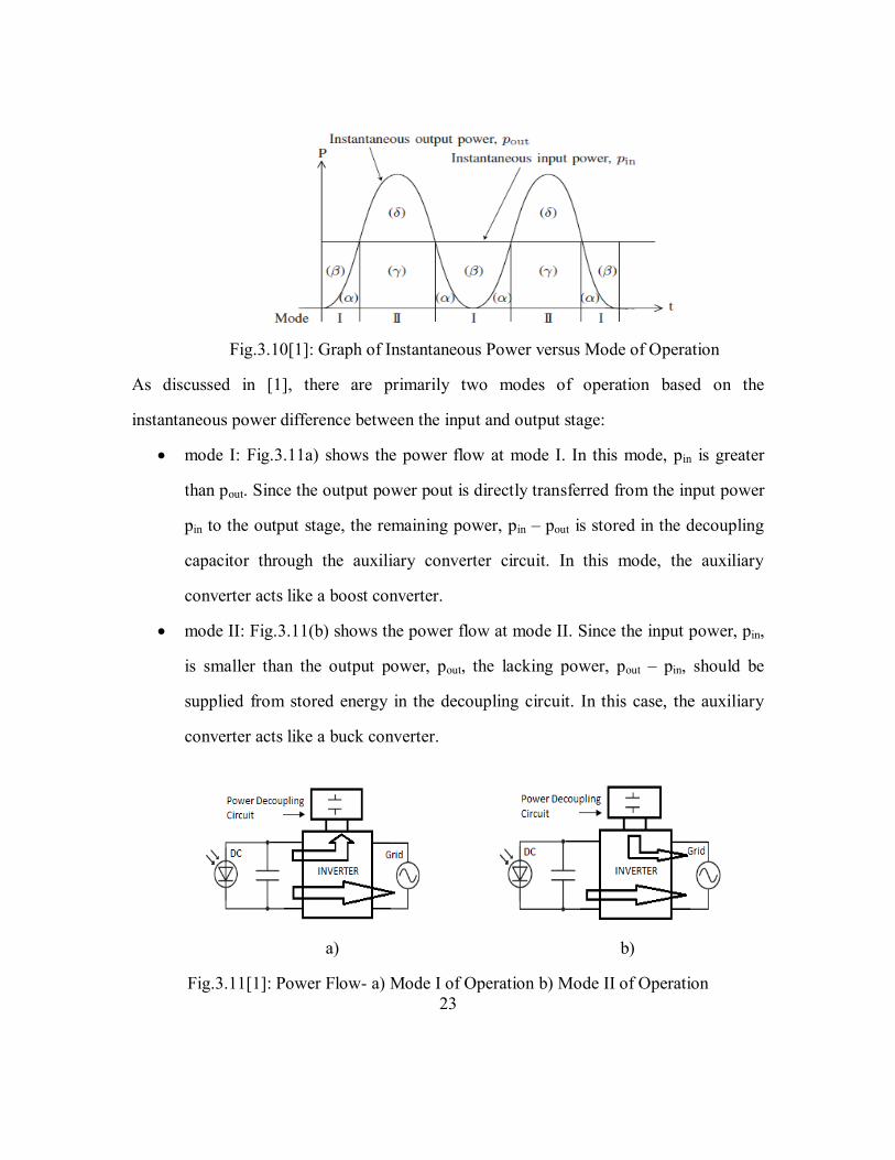
Fig.3.10 in next page, shows the relationship of instantaneous input power (pin)
and output power (pout), and the corresponding operation modes on the system. Since the
input power should be constant, whereas the output power fluctuates, the surplus or lack
of power among those should be stored in the power decoupling circuit.
23
Fig.3.10[1]: Graph of Instantaneous Power versus Mode of Operation
As discussed in [1], there are primarily two modes of operation based on the
instantaneous power difference between the input and output stage:
mode I: Fig.3.11a) shows the power flow at mode I. In this mode, pin is greater
than pout. Since the output power pout is directly transferred from the input power
pin to the output stage, the remaining power, pin – pout is stored in the decoupling
capacitor through the auxiliary converter circuit. In this mode, the auxiliary
converter acts like a boost converter.
mode II: Fig.3.11(b) shows the power flow at mode II. Since the input power, pin,
is smaller than the output power, pout, the lacking power, pout – pin, should be
supplied from stored energy in the decoupling circuit. In this case, the auxiliary
converter acts like a buck converter.
a) b)
Fig.3.11[1]: Power Flow- a) Mode I of Operation b) Mode II of Operation
24
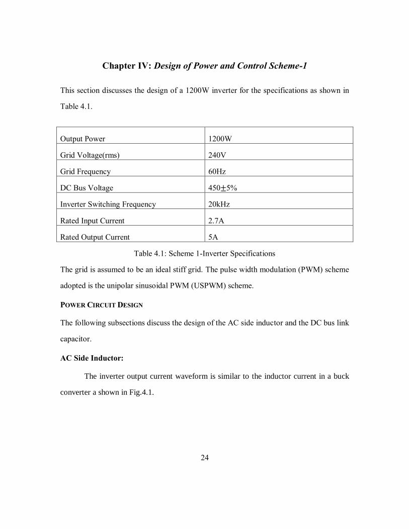
Chapter IV: Design of Power and Control Scheme-1
This section discusses the design of a 1200W inverter for the specifications as shown in
Table 4.1.
Output Power 1200W
Grid Voltage(rms) 240V
Grid Frequency 60Hz
DC Bus Voltage 450±5%
Inverter Switching Frequency 20kHz
Rated Input Current 2.7A
Rated Output Current 5A
Table 4.1: Scheme 1-Inverter Specifications
The grid is assumed to be an ideal stiff grid. The pulse width modulation (PWM) scheme
adopted is the unipolar sinusoidal PWM (USPWM) scheme.
POWER CIRCUIT DESIGN
The following subsections discuss the design of the AC side inductor and the DC bus link
capacitor.
AC Side Inductor:
The inverter output current waveform is similar to the inductor current in a buck
converter a shown in Fig.4.1.
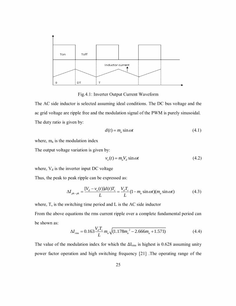
25
Fig.4.1: Inverter Output Current Waveform
The AC side inductor is selected assuming ideal conditions. The DC bus voltage and the
ac grid voltage are ripple free and the modulation signal of the PWM is purely sinusoidal.
The duty ratio is given by:
( ) sinad t m t (4.1)
where, ma is the modulation index
The output voltage variation is given by:
( ) sino a dv t m V t (4.2)
where, Vd is the inverter input DC voltage
Thus, the peak to peak ripple can be expressed as:
[ ( )] ( )
(1 sin )( sin )d o s d spk pk a a
V v t d t T V TI m t m t
L L
(4.3)
where, Ts is the switching time period and L is the AC side inductor
From the above equations the rms current ripple over a complete fundamental period can
be shown as:
20.163 (1.178 2.666 1.571)d srms a a a
V TI m m m
L (4.4)
The value of the modulation index for which the ∆Irms is highest is 0.628 assuming unity
power factor operation and high switching frequency [21] .The operating range of the

26
modulation index is calculated to lie between 0.71- 0.79 for the given variation in DC bus
voltage. Hence, 0.71 is selected as the worst case modulation index since ∆Irms is
maximum. A total harmonic distortion (THD) of 3% has been considered in the output
inductor current as per IEEE 1547 standards. The value of ΔIrms can be found using the
equation 4.5 given below [22].
1
rmsITHD
I
(4.5)
where, I1 is the fundamental component of the output grid current.
From simulation it is observed that, the USPWM technique introduces harmonics around
twice the switching frequency. The Fast Fourier Transform (FFT) analysis is performed
on the inverter output for the required modulation index of 0.75 and the magnitude of the
dominant voltage harmonic at twice the switching frequency is found to be 160.9V (peak
value). The frequency spectrum of the inverter output signal is shown in Fig.4.2.
Fig.4.2: Scheme 1- FFT Analysis of the Inverter Output
Considering the above cases, the worst case value of L is computed to be 1.1mH.
27
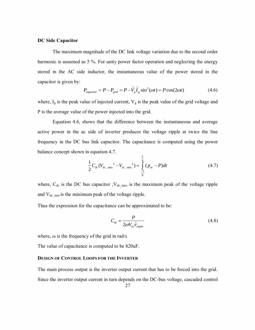
DC Side Capacitor
The maximum magnitude of the DC link voltage variation due to the second order
harmonic is assumed as 5 %. For unity power factor operation and neglecting the energy
stored in the AC side inductor, the instantaneous value of the power stored in the
capacitor is given by:
2sin ( ) cos(2 )capacitor grid g gP P P P V I t P t (4.6)
where, Ig is the peak value of injected current, Vg is the peak value of the grid voltage and
P is the average value of the power injected into the grid.
Equation 4.6, shows that the difference between the instantaneous and average
active power in the ac side of inverter produces the voltage ripple at twice the line
frequency in the DC bus link capacitor. The capacitance is computed using the power
balance concept shown in equation 4.7.
8
2 2
_ max _ min
8
1( ) ( )
2
T
dc dc dc ac
T
C V V p P dt
(4.7)
where, Cdc is the DC bus capacitor ,Vdc_max is the maximum peak of the voltage ripple
and Vdc_min is the minimum peak of the voltage ripple.
Thus the expression for the capacitance can be approximated to be:
2
dc
dc ripple
PC
V v (4.8)
where, ω is the frequency of the grid in rad/s
The value of capacitance is computed to be 820uF.
DESIGN OF CONTROL LOOPS FOR THE INVERTER
The main process output is the inverter output current that has to be forced into the grid.
Since the inverter output current in turn depends on the DC-bus voltage, cascaded control
28
is employed which consists of an outer voltage loop to regulate the DC bus voltage and
an inner current loop to regulate the output current of the inverter. The design is
discussed briefly in the following sections.
Inner Current Loop:
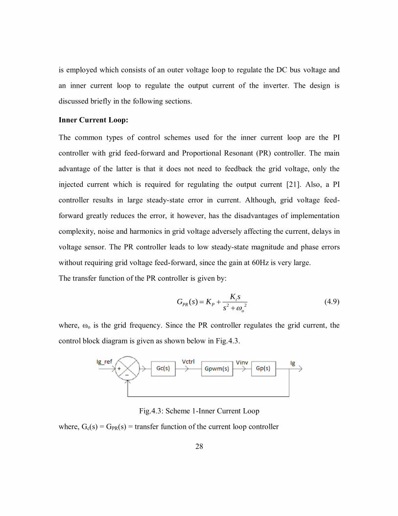
The common types of control schemes used for the inner current loop are the PI
controller with grid feed-forward and Proportional Resonant (PR) controller. The main
advantage of the latter is that it does not need to feedback the grid voltage, only the
injected current which is required for regulating the output current [21]. Also, a PI
controller results in large steady-state error in current. Although, grid voltage feed-
forward greatly reduces the error, it however, has the disadvantages of implementation
complexity, noise and harmonics in grid voltage adversely affecting the current, delays in
voltage sensor. The PR controller leads to low steady-state magnitude and phase errors
without requiring grid voltage feed-forward, since the gain at 60Hz is very large.
The transfer function of the PR controller is given by:
2 2( ) i
PR P
o
K sG s K
s
(4.9)
where, ωo is the grid frequency. Since the PR controller regulates the grid current, the
control block diagram is given as shown below in Fig.4.3.
Fig.4.3: Scheme 1-Inner Current Loop
where, Gc(s) = GPR(s) = transfer function of the current loop controller
29
The PWM block can be represented by a simple gain block since the switching frequency
of the inverter is very high. The small signal model of the PWM block is shown below:
( )
( )( )
inv dcpwm
ctrl tri
V s VG s
V s V (4.10)
where, Vdc is the DC bus voltage and Vtri is the peak value of the triangular signal.
The plant transfer function is the impedance on the load/grid side which is given by:
( ) 1
( )( )
g
p
inv
I sG s
V s R sL
(4.11)
where, R and L are the resistive and inductive components of the AC side filter.
Thus the effective transfer function of the system, as seen by the controller is:
( ) ( ) 1
( )( ) ( )
g inv dcsys
inv ctrl tri
I s V s VG s
V s V s R sL V
(4.12)
Selection of Gains for the PR Controller:
The bandwidth or cross over frequency of the current loop is chosen to be 1/10th of the
switching frequency i.e. 2 kHz so that, sufficient attenuation is provided for the switching
frequency harmonics. The PR controller is designed for a phase margin of 90 degrees as
shown in the formula below
1
c
P
sys
KG
(4.13)
where, Gsys is gain of rest of system at cross over frequency.
The controller parameters where computed to be:
KP=0.0287
Ki=0.5
The bode plot of the system is shown below in Fig.4.4 for this operating range
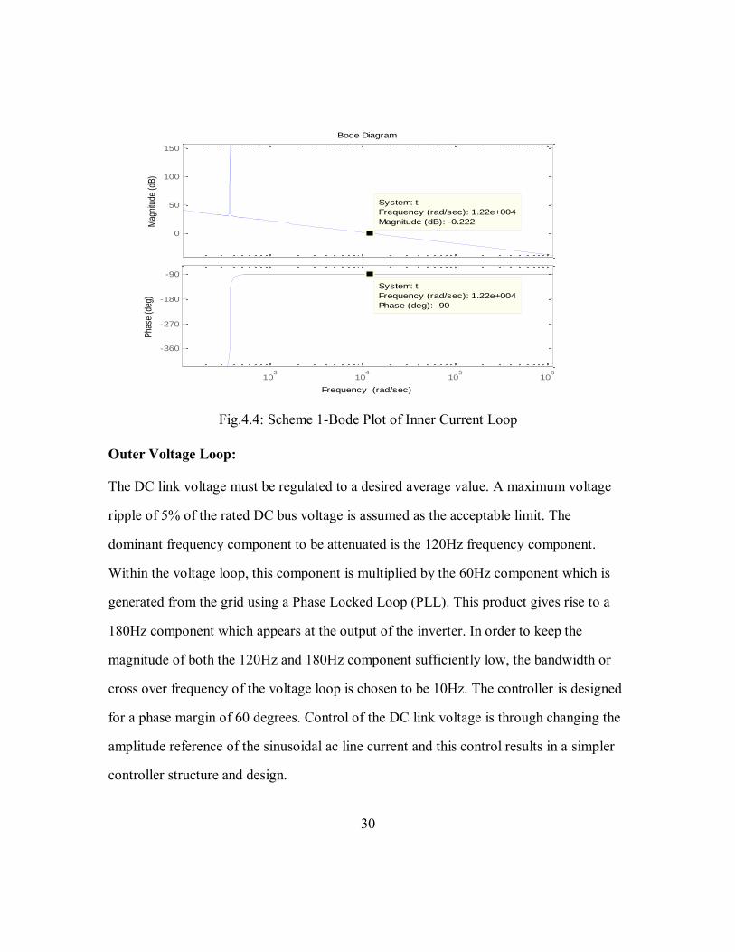
30
0
50
100
150
System: t
Frequency (rad/sec): 1.22e+004
Magnitude (dB): -0.222Mag
nitu
de (
dB)
103
104
105
106
-360
-270
-180
-90
System: t
Frequency (rad/sec): 1.22e+004
Phase (deg): -90
Pha
se (
deg)
Bode Diagram
Frequency (rad/sec)
Fig.4.4: Scheme 1-Bode Plot of Inner Current Loop
Outer Voltage Loop:
The DC link voltage must be regulated to a desired average value. A maximum voltage
ripple of 5% of the rated DC bus voltage is assumed as the acceptable limit. The
dominant frequency component to be attenuated is the 120Hz frequency component.
Within the voltage loop, this component is multiplied by the 60Hz component which is
generated from the grid using a Phase Locked Loop (PLL). This product gives rise to a
180Hz component which appears at the output of the inverter. In order to keep the
magnitude of both the 120Hz and 180Hz component sufficiently low, the bandwidth or
cross over frequency of the voltage loop is chosen to be 10Hz. The controller is designed
for a phase margin of 60 degrees. Control of the DC link voltage is through changing the
amplitude reference of the sinusoidal ac line current and this control results in a simpler
controller structure and design.
31
2
1.
2
DClink DClinkLi g
dC VP I v
dt (4.14)
where, CDClink is the DC link capacitance and VDClink is the voltage across the DC bus link
capacitor. Considering only the average or the DC component of the output power
equation 4.14 reduces to :
2
1 1
2 2
DClinkDClink Li g
dVC P I v
dt (4.15)
This is a linear system since VDClink2 is used as the variable instead of VDClink. Thus the
transfer function of the plant is given by the expression shown below:
2 ( )
( )( )
gDClinkP
Li DClink
VV sG s
I s sC (4.16)
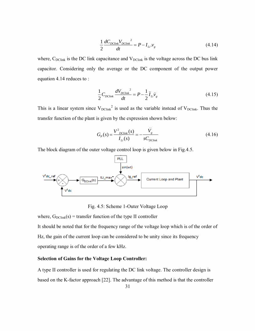
The block diagram of the outer voltage control loop is given below in Fig.4.5.
Fig. 4.5: Scheme 1-Outer Voltage Loop
where, GDClink(s) = transfer function of the type II controller
It should be noted that for the frequency range of the voltage loop which is of the order of
Hz, the gain of the current loop can be considered to be unity since its frequency
operating range is of the order of a few kHz.
Selection of Gains for the Voltage Loop Controller:
A type II controller is used for regulating the DC link voltage. The controller design is
based on the K-factor approach [22]. The advantage of this method is that the controller
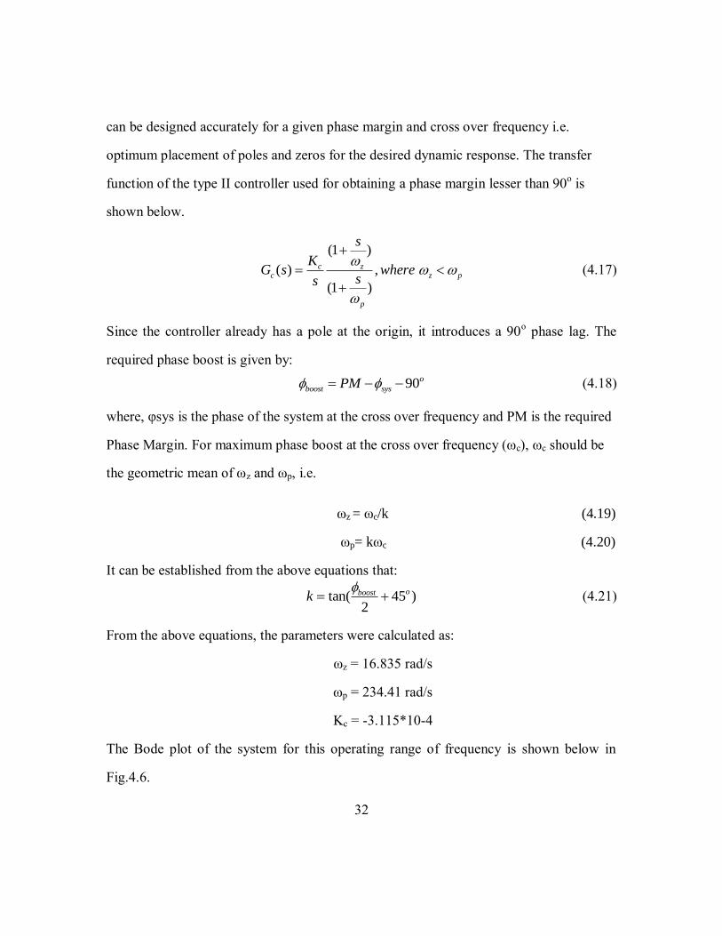
32
can be designed accurately for a given phase margin and cross over frequency i.e.
optimum placement of poles and zeros for the desired dynamic response. The transfer
function of the type II controller used for obtaining a phase margin lesser than 90o is
shown below.
(1 )
( ) ,
(1 )
c zc z p
p
s
KG s where
ss
(4.17)
Since the controller already has a pole at the origin, it introduces a 90o phase lag. The
required phase boost is given by:
90o
boost sysPM (4.18)
where, φsys is the phase of the system at the cross over frequency and PM is the required
Phase Margin. For maximum phase boost at the cross over frequency (ωc), ωc should be
the geometric mean of ωz and ωp, i.e.
ωz = ωc/k (4.19)
ωp= kωc (4.20)
It can be established from the above equations that:
tan( 45 )2
oboostk
(4.21)
From the above equations, the parameters were calculated as:
ωz = 16.835 rad/s
ωp = 234.41 rad/s
Kc = -3.115*10-4
The Bode plot of the system for this operating range of frequency is shown below in
Fig.4.6.

33
-100
-50
0
50
100
150
Mag
nitu
de (
dB)
System: g
Frequency (rad/sec): 62.8
Magnitude (dB): -0.00284
10-1
100
101
102
103
104
-180
-150
-120
System: g
Frequency (rad/sec): 62.8
Phase (deg): -120
Pha
se (
deg)
Bode Diagram
Frequency (rad/sec)
Fig.4.6: Scheme 1-Bode Plot of Outer Voltage Loop
ACTIVE POWER DECOUPLING CIRCUIT
The control loops designed for the inverter circuit are based on the assumption that the
input power source is constant, since a smaller value of DC bus capacitance is chosen
and hence they do not react to active power variations on the input side. In order to mete
out this demand, the active power decoupling circuit is built across the DC bus capacitor
in order to absorb the pulsating power as mentioned in the previous chapters.
The inductor in the decoupling circuit is chosen to be around the same value as the
inductor in the grid side. Thus an inductance of 1mH is selected. The minimum value of
capacitance, that can withstand a 5% ripple current as specified earlier is found to be
100μF, along with 100μF bus link capacitor, from simulation. Thus, a savings of
approximately 75.61% of capacitance that would have been used in the case of an
electrolytic capacitor is achieved. The pulsating power is shifted to the storage capacitor
in the auxiliary circuit. This could also be viewed as the decoupling circuit trying to
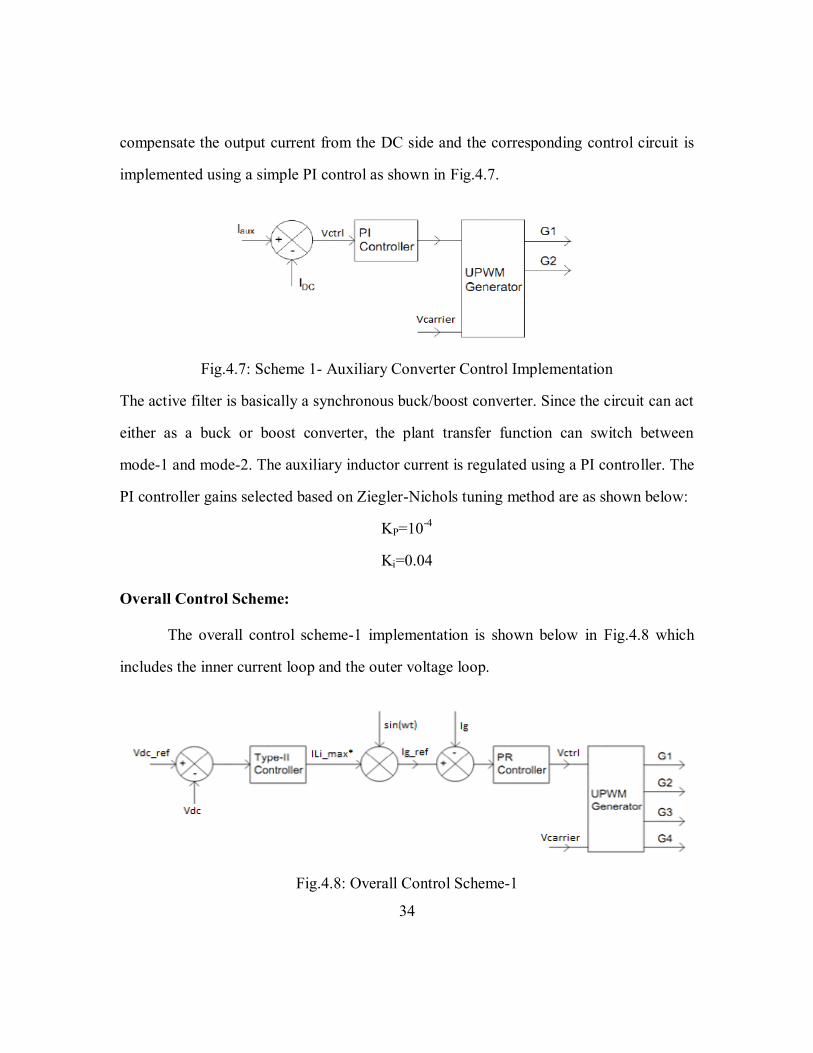
34
compensate the output current from the DC side and the corresponding control circuit is
implemented using a simple PI control as shown in Fig.4.7.
Fig.4.7: Scheme 1- Auxiliary Converter Control Implementation
The active filter is basically a synchronous buck/boost converter. Since the circuit can act
either as a buck or boost converter, the plant transfer function can switch between
mode-1 and mode-2. The auxiliary inductor current is regulated using a PI controller. The
PI controller gains selected based on Ziegler-Nichols tuning method are as shown below:
KP=10-4
Ki=0.04
Overall Control Scheme:
The overall control scheme-1 implementation is shown below in Fig.4.8 which
includes the inner current loop and the outer voltage loop.
Fig.4.8: Overall Control Scheme-1

35
Chapter V: Design of Power and Control Scheme-2
This section discusses the design of a 120W inverter for the specifications as shown in
Table 5.1.
Output Power 120W
Grid Voltage(rms) 25V
Grid Frequency 60Hz
DC Bus Voltage 35±5%
Inverter Switching Frequency 50kHz
Rated Input Current 3.428A
Rated Output Current 4.8A
Table 5.1: Scheme 2- Inverter Specifications
The grid is assumed to be an ideal stiff grid and the PWM scheme adopted is the
USPWM scheme here as in the case of scheme-1.
POWER CIRCUIT DESIGN
The following subsections discuss the design of the AC side inductor and the DC bus link
capacitor.
AC Side Inductor:
Considering similar conditions as in scheme-1 i.e ripple free DC bus voltage and AC grid
voltage, and purely sinusoidal modulation signal for the PWM, the inductor is selected.
The operating range of the modulation index is found to lie between 0.886-0.979 for the
given variation in DC bus voltage, and the worst case modulation index is selected as
0.886. From simulation, and performing Fast Fourier Analysis on the inverter output
36
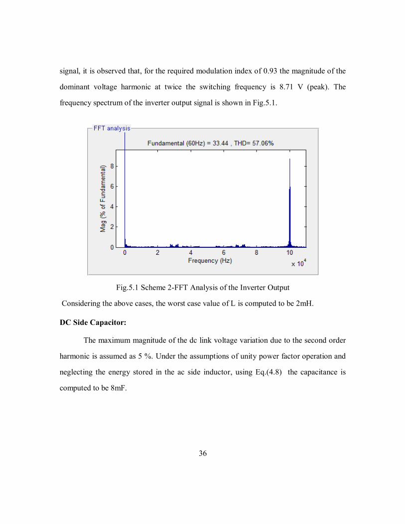
signal, it is observed that, for the required modulation index of 0.93 the magnitude of the
dominant voltage harmonic at twice the switching frequency is 8.71 V (peak). The
frequency spectrum of the inverter output signal is shown in Fig.5.1.
Fig.5.1 Scheme 2-FFT Analysis of the Inverter Output
Considering the above cases, the worst case value of L is computed to be 2mH.
DC Side Capacitor:
The maximum magnitude of the dc link voltage variation due to the second order
harmonic is assumed as 5 %. Under the assumptions of unity power factor operation and
neglecting the energy stored in the ac side inductor, using Eq.(4.8) the capacitance is
computed to be 8mF.
37
DESIGN OF CONTROL LOOPS FOR THE INVERTER
The cascaded PI control scheme with feed-forward is used here. The grid feed-forward
reduces the disturbance input and decreases the steady state error. The design and
performance of this control scheme will be studied in the following sections:
Inner Current Loop:
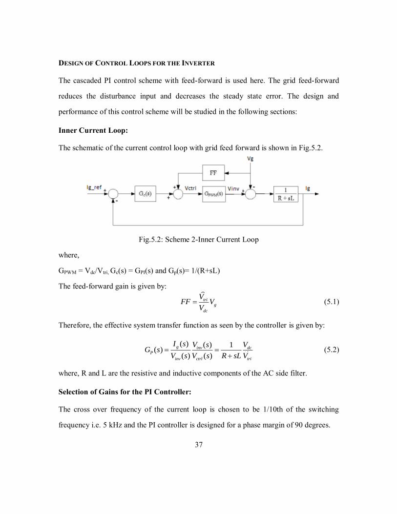
The schematic of the current control loop with grid feed forward is shown in Fig.5.2.
Fig.5.2: Scheme 2-Inner Current Loop
where,
GPWM = Vdc/Vtri, Gc(s) = GPI(s) and Gp(s)= 1/(R+sL)
The feed-forward gain is given by:
trig
dc
VFF V
V (5.1)
Therefore, the effective system transfer function as seen by the controller is given by:
( ) ( ) 1
( )( ) ( )
g inv dcP
inv ctrl tri
I s V s VG s
V s V s R sL V
(5.2)
where, R and L are the resistive and inductive components of the AC side filter.
Selection of Gains for the PI Controller:
The cross over frequency of the current loop is chosen to be 1/10th of the switching
frequency i.e. 5 kHz and the PI controller is designed for a phase margin of 90 degrees.
38
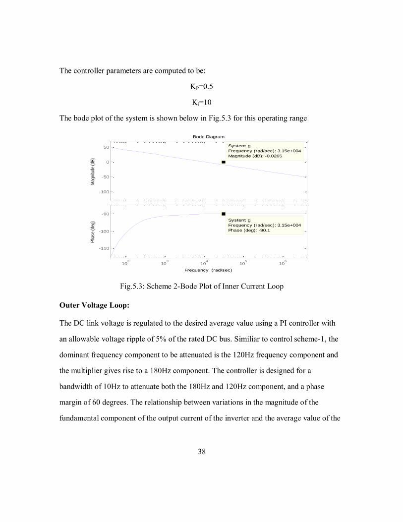
The controller parameters are computed to be:
KP=0.5
Ki=10
The bode plot of the system is shown below in Fig.5.3 for this operating range
-100
-50
0
50 System: g
Frequency (rad/sec): 3.15e+004
Magnitude (dB): -0.0265
Mag
nitu
de (
dB)
Bode Diagram
Frequency (rad/sec)
102
103
104
105
106
-110
-100
-90
System: g
Frequency (rad/sec): 3.15e+004
Phase (deg): -90.1
Pha
se (
deg)
Fig.5.3: Scheme 2-Bode Plot of Inner Current Loop
Outer Voltage Loop:
The DC link voltage is regulated to the desired average value using a PI controller with
an allowable voltage ripple of 5% of the rated DC bus. Similiar to control scheme-1, the
dominant frequency component to be attenuated is the 120Hz frequency component and
the multiplier gives rise to a 180Hz component. The controller is designed for a
bandwidth of 10Hz to attenuate both the 180Hz and 120Hz component, and a phase
margin of 60 degrees. The relationship between variations in the magnitude of the
fundamental component of the output current of the inverter and the average value of the
39
DC bus voltage can be calculated using the power balance equations and assuming that
the converter is lossless as given in equation 5.3.
dc c acP P P (5.3)
For determining the impact of the variation of the magnitude of the reference current on
the average value of the dc bus voltage, one neglects Pdc. Thus, equation 5.3 reduces to,
c acP P (5.4)
Finally,
21( )2 2
g g
dc dc
V IdC V
dt
(5.5)
Applying small perturbations about the operating point, equation 5.5 becomes:
2( )1
[ ( ) ]2 2
g g g
dc dc dc
V I idC V v
dt
(5.6)
Neglecting steady state values and square of small perturbations and after some
manipulations, finally we get
( )
( ) 2
gdc
g dc dc
VV s
I s sC V
(5.7)
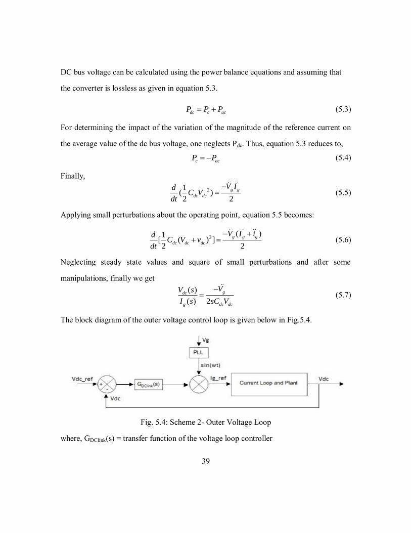
The block diagram of the outer voltage control loop is given below in Fig.5.4.
Fig. 5.4: Scheme 2- Outer Voltage Loop
where, GDClink(s) = transfer function of the voltage loop controller
40
It should be noted that for the frequency range of the voltage loop which is of the order of
Hz, the gain of the current loop can be considered to be unity since its frequency
operating range is of the order of a few kHz.
Selection of Gains for the Voltage Loop Controller:
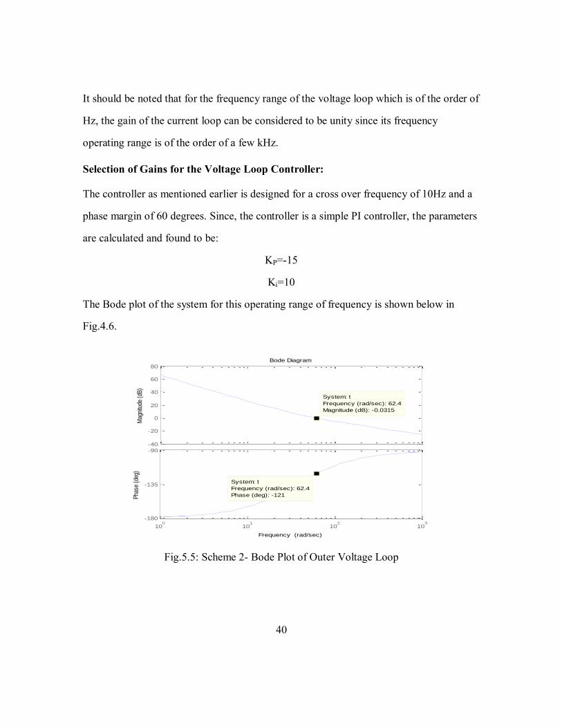
The controller as mentioned earlier is designed for a cross over frequency of 10Hz and a
phase margin of 60 degrees. Since, the controller is a simple PI controller, the parameters
are calculated and found to be:
KP=-15
Ki=10
The Bode plot of the system for this operating range of frequency is shown below in
Fig.4.6.
-40
-20
0
20
40
60
80
System: t
Frequency (rad/sec): 62.4
Magnitude (dB): -0.0315
Mag
nitu
de (
dB)
100
101
102
103
-180
-135
-90
System: t
Frequency (rad/sec): 62.4
Phase (deg): -121Pha
se (
deg)
Bode Diagram
Frequency (rad/sec)
Fig.5.5: Scheme 2- Bode Plot of Outer Voltage Loop
41
Active Power Decoupling Circuit:
In order to absorb the power pulsation, the active power decoupling circuit is
implemented as a Half-Bridge topology, similar to control scheme-1. The inductor in the
decoupling circuit is chosen to be around the same value as the inductor in the grid side
i.e 2mH. The minimum value of capacitance, that can withstand a 5% ripple current was
found to be 850uF along with 1mF in the DC bus link capacitor from simulation. Thus, a
savings of approximately 77.5% of capacitance that would have been used in the case of
an electrolytic capacitor is achieved. The auxiliary inductor current is regulated using a PI
controller. The PI controller gains selected based on Ziegler-Nichols tuning method are
as shown below:
KP=5*10-5
Ki=5*10-4
When the power decoupling circuit is used, the value of the PI controller parameters used
in the Outer voltage control loop of the inverter is modified as:
KP= -5.3
Ki=10
Overall Control Scheme:
The overall control scheme-2 implementation is shown below in Fig.5.6 which includes
both the inner current loop and the outer voltage loop.
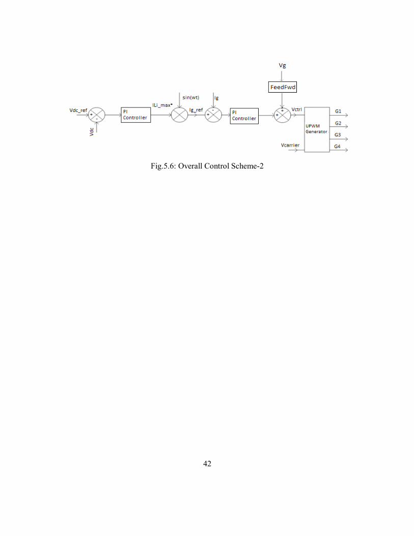
42
Fig.5.6: Overall Control Scheme-2
43
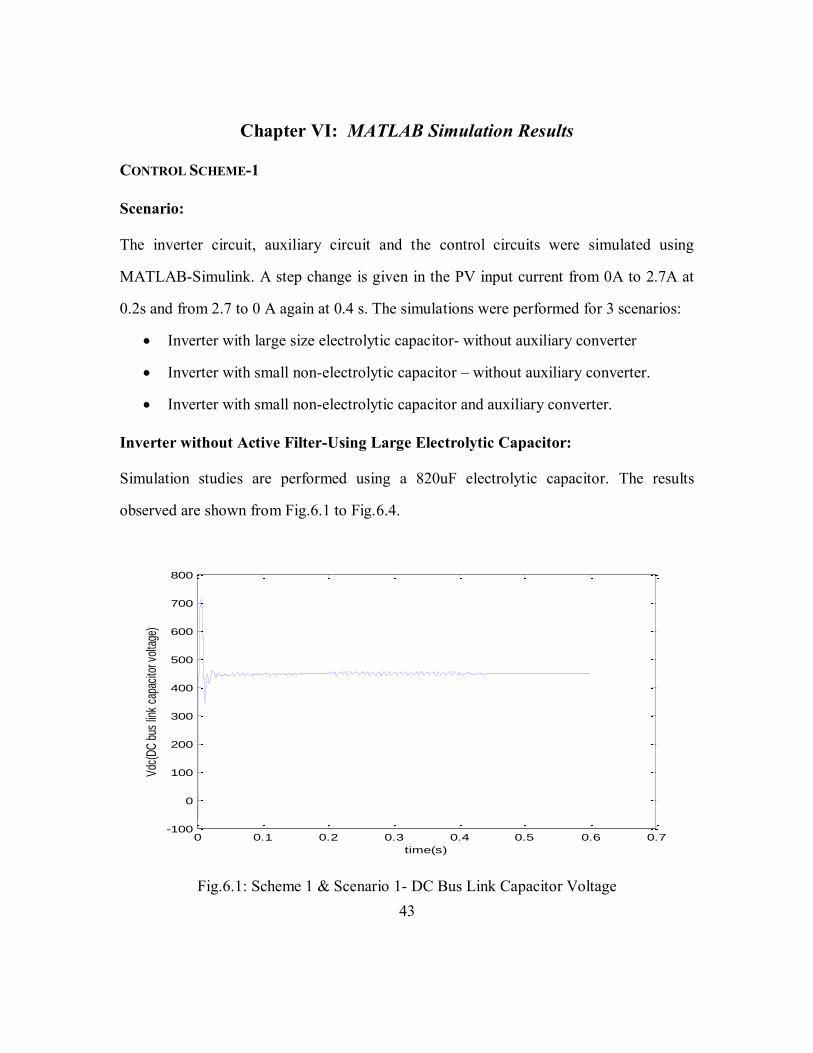
Chapter VI: MATLAB Simulation Results
CONTROL SCHEME-1
Scenario:
The inverter circuit, auxiliary circuit and the control circuits were simulated using
MATLAB-Simulink. A step change is given in the PV input current from 0A to 2.7A at
0.2s and from 2.7 to 0 A again at 0.4 s. The simulations were performed for 3 scenarios:
Inverter with large size electrolytic capacitor- without auxiliary converter
Inverter with small non-electrolytic capacitor – without auxiliary converter.
Inverter with small non-electrolytic capacitor and auxiliary converter.
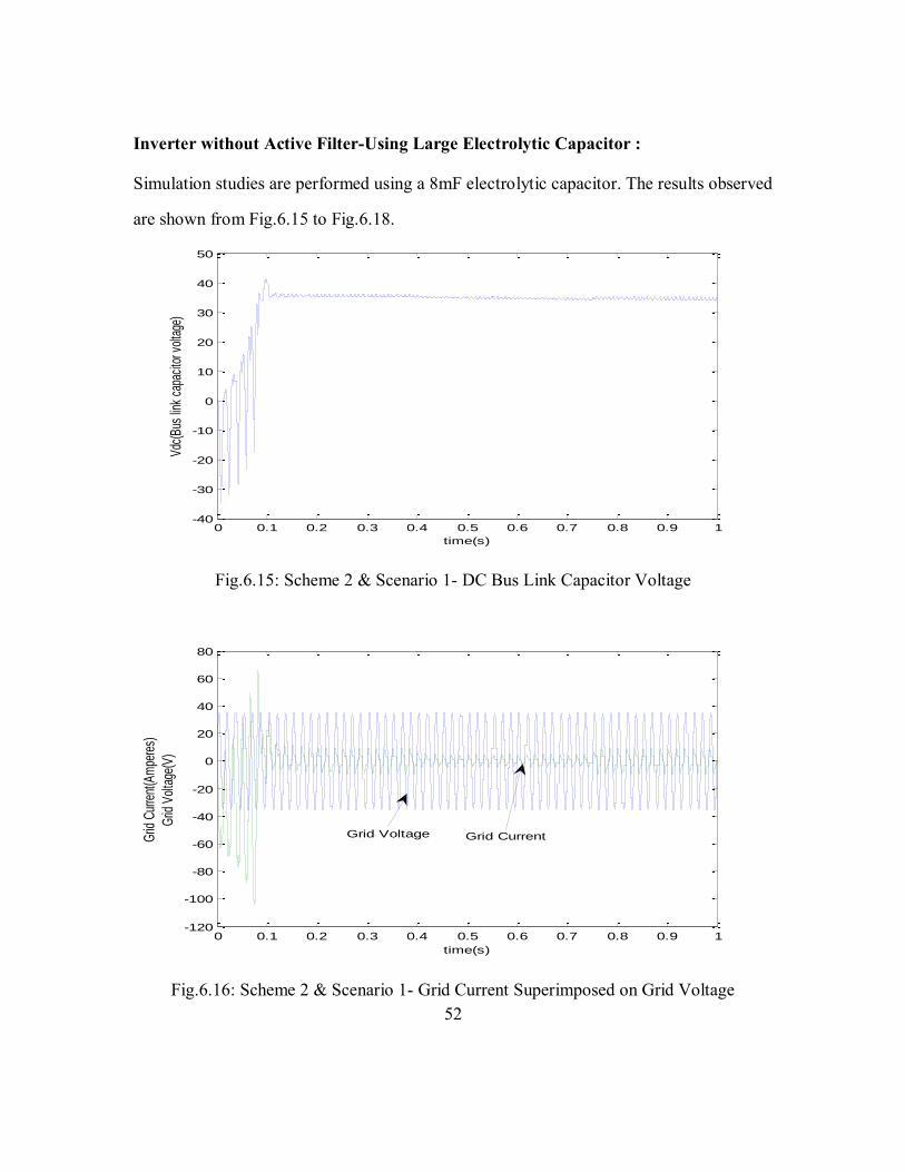
Inverter without Active Filter-Using Large Electrolytic Capacitor:
Simulation studies are performed using a 820uF electrolytic capacitor. The results
observed are shown from Fig.6.1 to Fig.6.4.
0 0.1 0.2 0.3 0.4 0.5 0.6 0.7-100
0
100
200
300
400
500
600
700
800
Vdc
(DC
bus
link
cap
acito
r vol
tage
)
time(s)
Fig.6.1: Scheme 1 & Scenario 1- DC Bus Link Capacitor Voltage
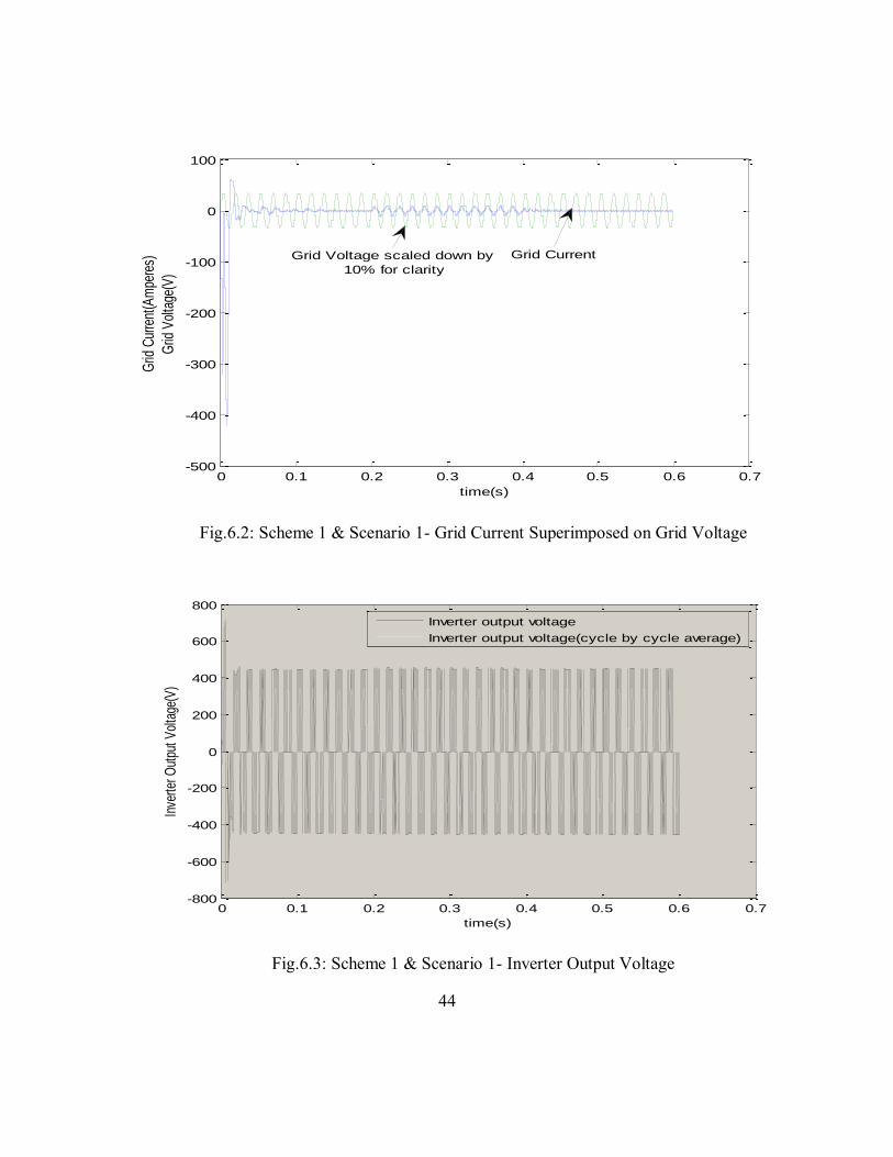
44
0 0.1 0.2 0.3 0.4 0.5 0.6 0.7-500
-400
-300
-200
-100
0
100
time(s)
Grid
Cur
rent
(Am
pere
s)
Grid
Vol
tage
(V)
Grid CurrentGrid Voltage scaled down by
10% for clarity
Fig.6.2: Scheme 1 & Scenario 1- Grid Current Superimposed on Grid Voltage
0 0.1 0.2 0.3 0.4 0.5 0.6 0.7-800
-600
-400
-200
0
200
400
600
800
time(s)
Inve
rter O
utpu
t Vol
tage
(V)
Inverter output voltage
Inverter output voltage(cycle by cycle average)
Fig.6.3: Scheme 1 & Scenario 1- Inverter Output Voltage

45
0 0.1 0.2 0.3 0.4 0.5 0.6 0.7-400
-300
-200
-100
0
100
200
300
400
500
time(s)
Inve
rter
Inp
ut C
urre
nt(A
mpe
res)
Inverter input current
Inverter input current(cycle by cycle average)
Fig.6.4: Scheme 1 & Scenario 1- Inverter Input Current
As seen in Fig.6.1, the peak to peak ripple in the DC link voltage waveform is observed
to be around 11.6 V i.e. around 1.3% ripple, which is well within the 5% defined limit of
operation. The grid current is also observed to be closely synchronized with the grid
voltage and has less distortion.
Inverter without Active Filter-Using Small Non-Electrolytic Capacitor:
A small non-electrolytic 100uF capacitor is used in the following simulation. The
observed waveforms are shown from Fig.6.5 to Fig.6.8.

46
0 0.1 0.2 0.3 0.4 0.5 0.6 0.7-200
0
200
400
600
800
1000
time(s)
Vdc
(Bus
link
cap
acito
r vol
tage
)
Fig.6.5: Scheme 1 & Scenario 2- DC Bus Link Capacitor Voltage
0 0.1 0.2 0.3 0.4 0.5 0.6 0.7-150
-100
-50
0
50
100
150
time(s)
Grid
Cur
rent
(Am
pere
s)
Grid
Vol
tage
(V)
Grid CurrentGrid Voltage scaled down
by 10% for clarity
Fig.6.6: Scheme 1 & Scenario 2- Grid Current Superimposed on Grid Voltage

47
0 0.1 0.2 0.3 0.4 0.5 0.6 0.7-1000
-800
-600
-400
-200
0
200
400
600
800
1000
time(s)
Inve
rter O
utpu
t Vol
tage
(V)
Inverter output voltage
Inverter output voltage(cycle by cycle average)
Fig.6.7: Scheme 1 & Scenario 2- Inverter Output Voltage
0 0.1 0.2 0.3 0.4 0.5 0.6 0.7-150
-100
-50
0
50
100
150
time(s)
Inve
rter
Inp
ut C
urre
nt(A
mpe
res)
Inverter input current
Inverter input current(cycle by cycle average)
Fig.6.8: Scheme 1 & Scenario 2- Inverter Input Current
48
As seen in Fig.6.5, the peak to peak ripple in the DC bus link capacitor voltage is around
93 V, i.e. 10.3% ripple, which is very high compared to the prescribed limitations. The
grid current, is also observed to be highly distorted though synchronized with the grid
voltage.
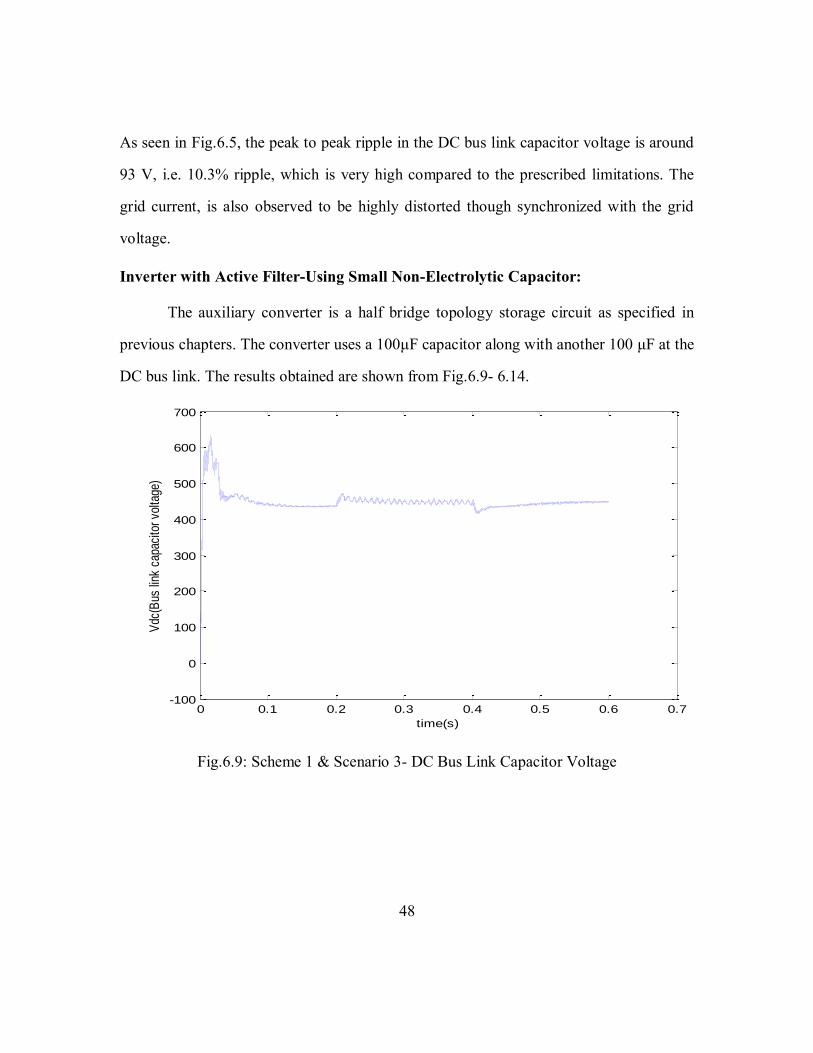
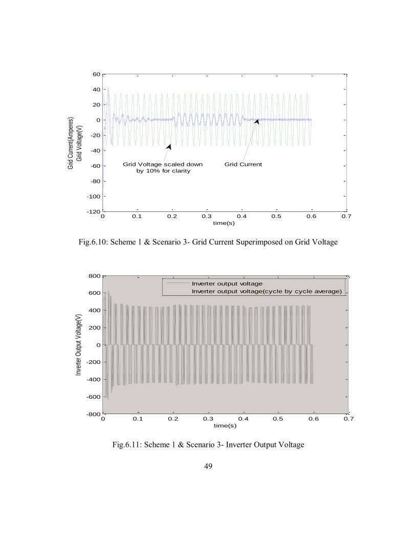
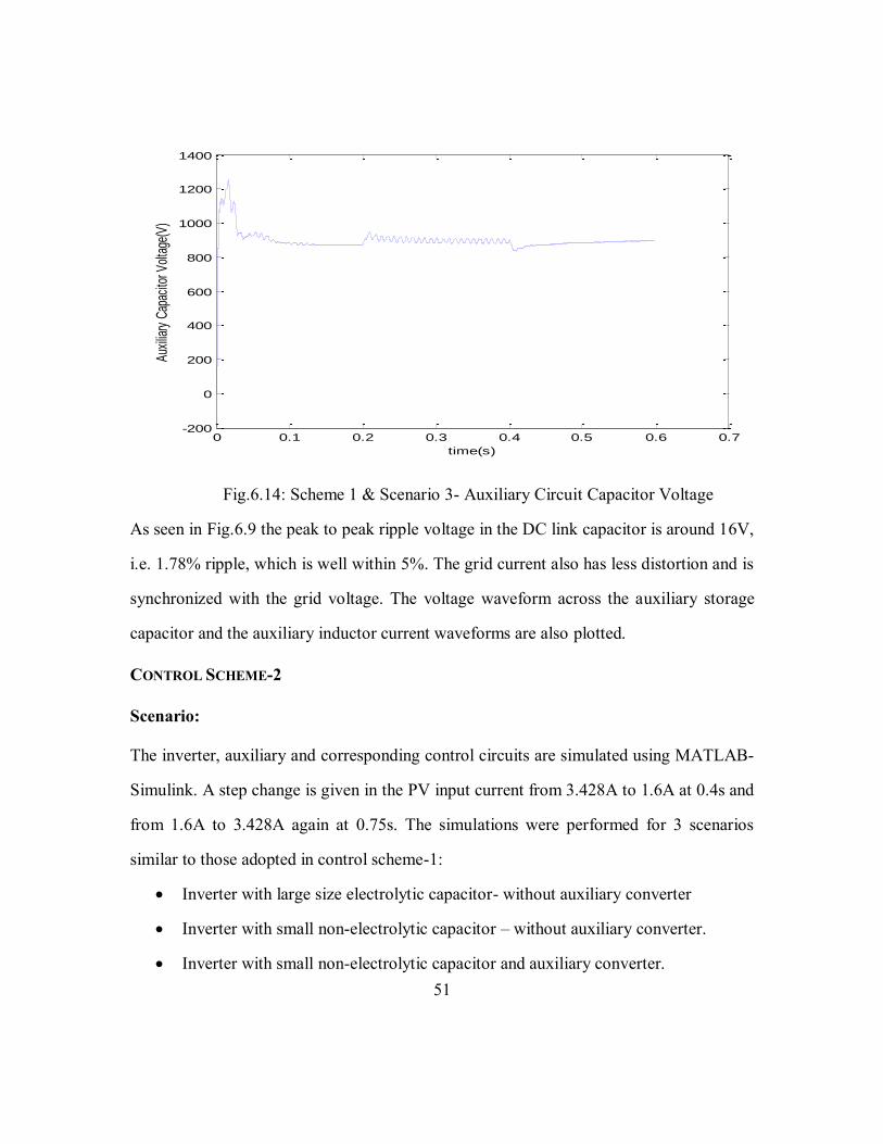
Inverter with Active Filter-Using Small Non-Electrolytic Capacitor:
The auxiliary converter is a half bridge topology storage circuit as specified in
previous chapters. The converter uses a 100μF capacitor along with another 100 μF at the
DC bus link. The results obtained are shown from Fig.6.9- 6.14.
0 0.1 0.2 0.3 0.4 0.5 0.6 0.7-100
0
100
200
300
400
500
600
700
time(s)
Vdc
(Bus
link
cap
acito
r vo
ltage
)
Fig.6.9: Scheme 1 & Scenario 3- DC Bus Link Capacitor Voltage
49
0 0.1 0.2 0.3 0.4 0.5 0.6 0.7-120
-100
-80
-60
-40
-20
0
20
40
60
time(s)
Grid
Cur
rent
(Am
pere
s)
Grid
Vol
tage
(V)
Grid CurrentGrid Voltage scaled down
by 10% for clarity
Fig.6.10: Scheme 1 & Scenario 3- Grid Current Superimposed on Grid Voltage
0 0.1 0.2 0.3 0.4 0.5 0.6 0.7-800
-600
-400
-200
0
200
400
600
800
time(s)
Inve
rter O
utpu
t Vol
tage
(V)
Inverter output voltage
Inverter output voltage(cycle by cycle average)
Fig.6.11: Scheme 1 & Scenario 3- Inverter Output Voltage

50
0 0.1 0.2 0.3 0.4 0.5 0.6 0.7-120
-100
-80
-60
-40
-20
0
20
40
60
time(s)
Inve
rter I
nput
Cur
rent
(Am
pere
s)
Inverter input current
Inverter input current(cycle by cycle average)
Fig.6.12: Scheme 1 & Scenario 3- Inverter Input Current
0 0.1 0.2 0.3 0.4 0.5 0.6 0.7-40
-20
0
20
40
60
80
100
120
time(s)
Aux
iliar
y In
duct
or C
urre
nt(A
mpe
res)
Fig.6.13: Scheme 1 & Scenario 3- Auxiliary Circuit Inductor Current
51
0 0.1 0.2 0.3 0.4 0.5 0.6 0.7-200
0
200
400
600
800
1000
1200
1400
time(s)
Auxi
liary
Cap
acito
r Vol
tage
(V)
Fig.6.14: Scheme 1 & Scenario 3- Auxiliary Circuit Capacitor Voltage
As seen in Fig.6.9 the peak to peak ripple voltage in the DC link capacitor is around 16V,
i.e. 1.78% ripple, which is well within 5%. The grid current also has less distortion and is
synchronized with the grid voltage. The voltage waveform across the auxiliary storage
capacitor and the auxiliary inductor current waveforms are also plotted.
CONTROL SCHEME-2
Scenario:
The inverter, auxiliary and corresponding control circuits are simulated using MATLAB-
Simulink. A step change is given in the PV input current from 3.428A to 1.6A at 0.4s and
from 1.6A to 3.428A again at 0.75s. The simulations were performed for 3 scenarios
similar to those adopted in control scheme-1:
Inverter with large size electrolytic capacitor- without auxiliary converter
Inverter with small non-electrolytic capacitor – without auxiliary converter.
Inverter with small non-electrolytic capacitor and auxiliary converter.
52
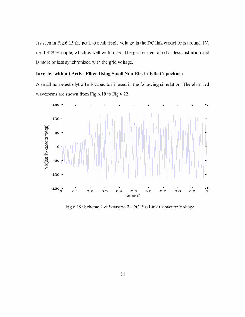
Inverter without Active Filter-Using Large Electrolytic Capacitor :
Simulation studies are performed using a 8mF electrolytic capacitor. The results observed
are shown from Fig.6.15 to Fig.6.18.
0 0.1 0.2 0.3 0.4 0.5 0.6 0.7 0.8 0.9 1-40
-30
-20
-10
0
10
20
30
40
50
time(s)
Vdc(
Bus
link
capa
cito
r vol
tage
)
Fig.6.15: Scheme 2 & Scenario 1- DC Bus Link Capacitor Voltage
0 0.1 0.2 0.3 0.4 0.5 0.6 0.7 0.8 0.9 1-120
-100
-80
-60
-40
-20
0
20
40
60
80
time(s)
Grid
Cur
rent
(Am
pere
s)
Grid
Vol
tage
(V)
Grid Voltage Grid Current
Fig.6.16: Scheme 2 & Scenario 1- Grid Current Superimposed on Grid Voltage

53
0 0.1 0.2 0.3 0.4 0.5 0.6 0.7 0.8 0.9 1-100
-50
0
50
100
time(s)
Invert
er
Outp
ut
Voltage(V
)
Inverter output voltage
Inverter output voltage(cycle by cycle average)
Fig.6.17: Scheme 2 & Scenario 1- Inverter Output Voltage
0 0.1 0.2 0.3 0.4 0.5 0.6 0.7 0.8 0.9 1-200
-150
-100
-50
0
50
100
150
200
time(s)
Inve
rter I
nput
Cur
rent
(Am
pere
s)
Inverter input current(cycle by cycle average)
Inverter input current
Fig.6.18: Scheme 2 & Scenario 1- Inverter Input Current
54
As seen in Fig.6.15 the peak to peak ripple voltage in the DC link capacitor is around 1V,
i.e. 1.428 % ripple, which is well within 5%. The grid current also has less distortion and
is more or less synchronized with the grid voltage.
Inverter without Active Filter-Using Small Non-Electrolytic Capacitor :
A small non-electrolytic 1mF capacitor is used in the following simulation. The observed
waveforms are shown from Fig.6.19 to Fig.6.22.
0 0.1 0.2 0.3 0.4 0.5 0.6 0.7 0.8 0.9 1-150
-100
-50
0
50
100
150
time(s)
Vdc
(Bus
link
cap
acito
r vol
tage
)
Fig.6.19: Scheme 2 & Scenario 2- DC Bus Link Capacitor Voltage
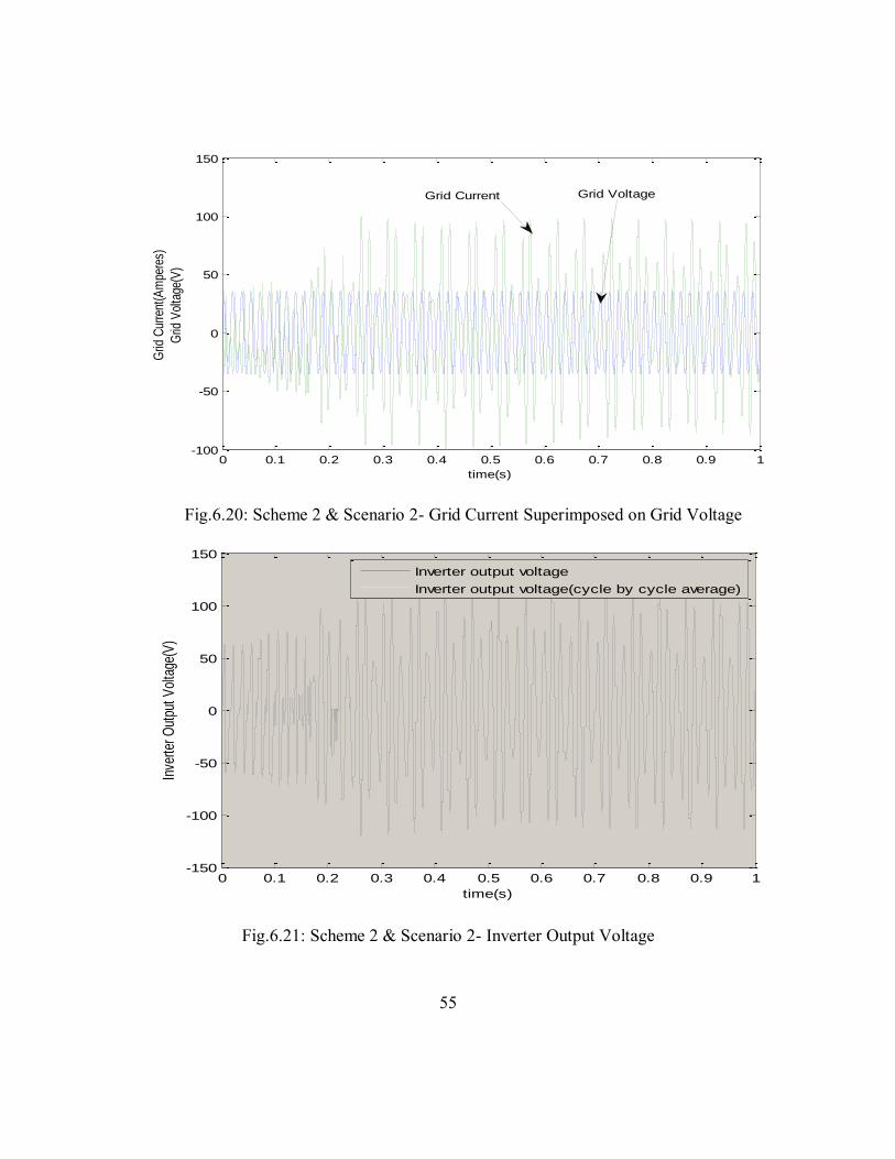
55
0 0.1 0.2 0.3 0.4 0.5 0.6 0.7 0.8 0.9 1-100
-50
0
50
100
150
time(s)
Grid
Cur
rent
(Am
pere
s)
Grid
Vol
tage
(V)
Grid Current Grid Voltage
Fig.6.20: Scheme 2 & Scenario 2- Grid Current Superimposed on Grid Voltage
0 0.1 0.2 0.3 0.4 0.5 0.6 0.7 0.8 0.9 1-150
-100
-50
0
50
100
150
time(s)
Inve
rter O
utpu
t Vol
tage
(V)
Inverter output voltage
Inverter output voltage(cycle by cycle average)
Fig.6.21: Scheme 2 & Scenario 2- Inverter Output Voltage
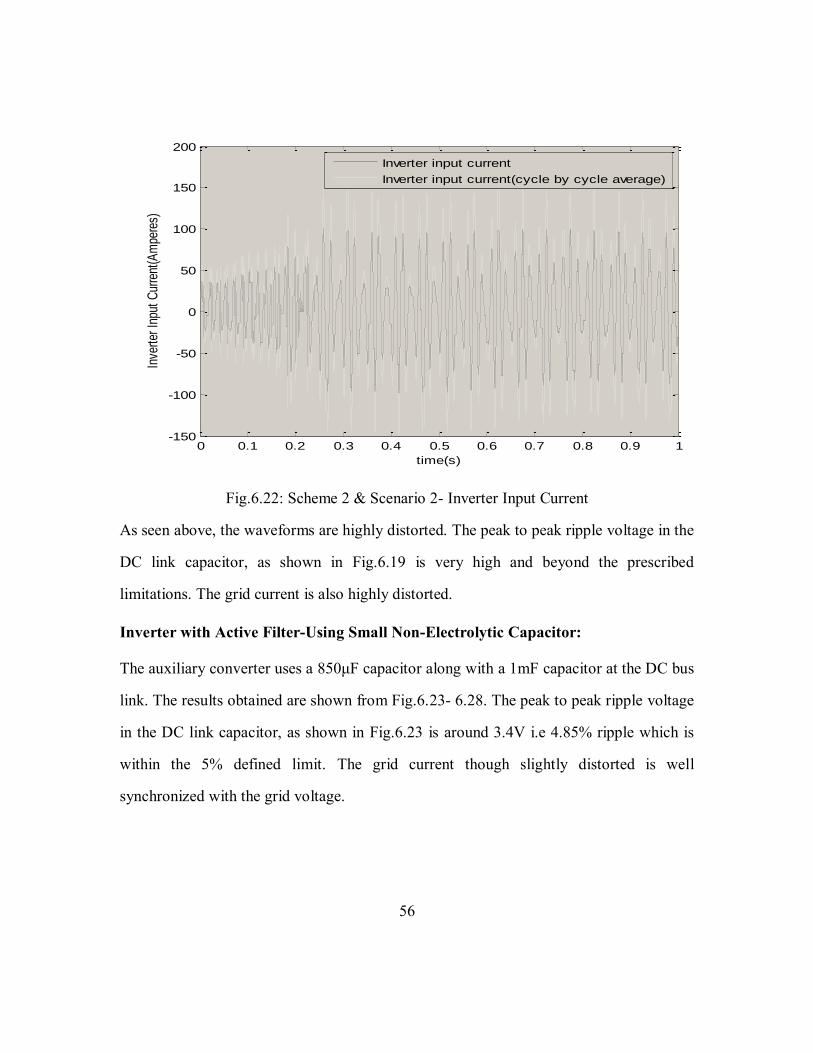
56
0 0.1 0.2 0.3 0.4 0.5 0.6 0.7 0.8 0.9 1-150
-100
-50
0
50
100
150
200
time(s)
Inve
rter
Inp
ut C
urre
nt(A
mpe
res)
Inverter input current
Inverter input current(cycle by cycle average)
Fig.6.22: Scheme 2 & Scenario 2- Inverter Input Current
As seen above, the waveforms are highly distorted. The peak to peak ripple voltage in the
DC link capacitor, as shown in Fig.6.19 is very high and beyond the prescribed
limitations. The grid current is also highly distorted.
Inverter with Active Filter-Using Small Non-Electrolytic Capacitor:
The auxiliary converter uses a 850μF capacitor along with a 1mF capacitor at the DC bus
link. The results obtained are shown from Fig.6.23- 6.28. The peak to peak ripple voltage
in the DC link capacitor, as shown in Fig.6.23 is around 3.4V i.e 4.85% ripple which is
within the 5% defined limit. The grid current though slightly distorted is well
synchronized with the grid voltage.

57
0 0.1 0.2 0.3 0.4 0.5 0.6 0.7 0.8 0.9 1-100
-50
0
50
100
150
time(s)
Vdc
(Bus
link
cap
acito
r vo
ltage
)
Fig.6.23: Scheme 2 & Scenario 3- DC Bus Link Capacitor Voltage
0 0.1 0.2 0.3 0.4 0.5 0.6 0.7 0.8 0.9 1-100
-80
-60
-40
-20
0
20
40
60
80
100
time(s)
Grid
Cur
rent
(Am
pere
s)
Grid
Vol
tage
(V)
Grid Voltage Grid Current
Fig.6.24: Scheme 2 & Scenario 3- Grid Current Superimposed on Grid Voltage
58
0 0.1 0.2 0.3 0.4 0.5 0.6 0.7 0.8 0.9 1-150
-100
-50
0
50
100
150
time(s)
Inve
rter O
utpu
t Vol
tage
(V)
Inverter output voltage
Inverter output voltage(cycle by cycle average)
Fig.6.25: Scheme 2 & Scenario 3- Inverter Output Voltage
0 0.1 0.2 0.3 0.4 0.5 0.6 0.7 0.8 0.9 1-150
-100
-50
0
50
100
150
time(s)
Inve
rter I
nput
Cur
rent
(Am
pere
s)
Inverter input current
Inverter input current(cycle by cycle average)
Fig.6.26: Scheme 2 & Scenario 3- Inverter Input Current
59
0 0.1 0.2 0.3 0.4 0.5 0.6 0.7 0.8 0.9 1-150
-100
-50
0
50
100
150
time(s)
Aux
iliar
y In
duct
or C
urre
nt(A
mpe
res)
Fig.6.27: Scheme 2 & Scenario 3- Auxiliary Circuit Inductor Current
0 0.1 0.2 0.3 0.4 0.5 0.6 0.7 0.8 0.9 1-100
-50
0
50
100
150
200
time(s)
Aux
iliar
y C
apac
itor
Vol
tage
(V)
Fig.6.28: Scheme 2 & Scenario 3- Auxiliary Circuit Capacitor Voltage
60
SIMULINK MODEL
The MATLAB Simulink model of the 2 control schemes is shown below in Fig.6.29.
Fig.6.29: MATLAB Simulink Model of the Two Control Schemes

61
Chapter VII: Electronic Circuit Design and Simulation
The non-ideal characteristics of the model has been analyzed and verified by
designing the model with the control-scheme 2 and simulating the same in LTSPICE,
which is a analog electronics circuit simulator of Linear Technology. The following
sections will discuss the design of the different components of the circuit.
INVERTER AND FIRING CIRCUIT
The switches used for the inverter circuit has to be a fast and reliable power
electronic switch. Hence, the IRFZ44N, advanced HEXFET Power MOSFET produced
by International rectifiers is used. They also have very small on-resistance combined with
the fast switching and ruggedness [23].
The USPWM scheme is implemented in the firing circuit, to generate the gating
pulses for the switches. The LT1716 μ-power precision rail-rail comparator is used for
comparing the modulating waveform generated by the control circuit and the sawtooth
waveform that controls the switching frequency[24]. The switching frequency has been
limited to 1kHz since the comparator does not respond accurately to very high
frequencies. In order to achieve a fairly fast switching of the MOSFETS which is
dependent on the input resistance and Ciss i.e the input capacitance of 1470pF, the
comparator output is amplified by a gain of 50 using an op-amp. The op-amp used is a
LT1007A, and it has extremely low noise and high precision and speed performance[25].
In addition, the differential voltage amplication is also very high 20V/μV driving a 2kΩ
load to ±12V. The LT1007A is also used in all the other sections of the complete
schematic. The LTSPICE model of the Inverter and corresponding firing circuit is shown
below in Fig.7.1.

62
Fig.7.1: LTSPICE Model-Inverter and PWM Firing Circuit
VOLTAGE CONTROL SCHEME
The PI controller is implemented using op-amps. The gain parameters are found
to be KP=0.05 and Ki=0.005, through trial and error and are variant from the values used
in the ideal MATLAB simulation. The LTSPICE model of the voltage control scheme is
shown below in Fig.7.2.
Fig.7.2: LTSPICE Model-Voltage Control Scheme
63
MULTIPLIER CIRCUIT
The analog multiplier circuit used to generate the current reference for the current control
scheme is shown below in Fig.7.4. It is implemented using 2 logarithmic op-amp circuits,
a summer circuits and an exponential op-amp circuit [26] as shown in Fig.73. The output
of the circuit is given by:
1 2
out
s
VVV
I R (7.1)
where, V1 and V2 are the two input voltages, Is is the diode current if it is inverse-
polarized and R is the common resistance used in all the op-amps of the multiplier circuit.
The most necessary condition with regard this implementation is that both V1 and V2
have to be positive since, the logarithmic function holds good only for positive
arguments. Thus, a dc offset of +1 V is given to the sinusoidal 60Hz reference with which
the output of the voltage control loop is multiplied and compensated after the
multiplication operation. The value of R is selected to be 1kΩ.
Fig.7.3: Block Diagram of the Analog Multiplier Circuit
The MOSFET implementation of the analog multiplier is less complicated with fewer
components, but the diode implementation works for a wider range of inputs and is thus
recommended.
log(x)
log(x)
V1
V2
Σ exp() Vout
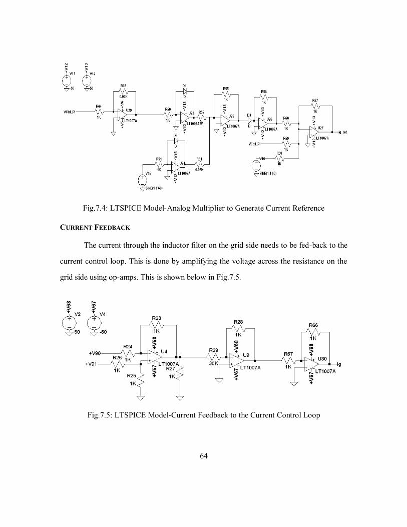
64
Fig.7.4: LTSPICE Model-Analog Multiplier to Generate Current Reference
CURRENT FEEDBACK
The current through the inductor filter on the grid side needs to be fed-back to the
current control loop. This is done by amplifying the voltage across the resistance on the
grid side using op-amps. This is shown below in Fig.7.5.
Fig.7.5: LTSPICE Model-Current Feedback to the Current Control Loop
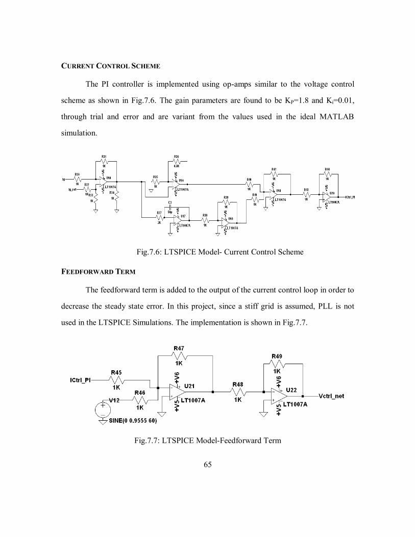
65
CURRENT CONTROL SCHEME
The PI controller is implemented using op-amps similar to the voltage control
scheme as shown in Fig.7.6. The gain parameters are found to be KP=1.8 and Ki=0.01,
through trial and error and are variant from the values used in the ideal MATLAB
simulation.
Fig.7.6: LTSPICE Model- Current Control Scheme
FEEDFORWARD TERM
The feedforward term is added to the output of the current control loop in order to
decrease the steady state error. In this project, since a stiff grid is assumed, PLL is not
used in the LTSPICE Simulations. The implementation is shown in Fig.7.7.
Fig.7.7: LTSPICE Model-Feedforward Term
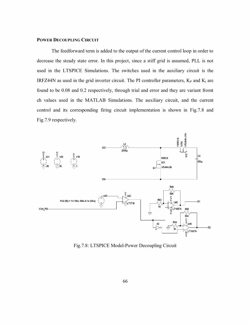
66
POWER DECOUPLING CIRCUIT
The feedforward term is added to the output of the current control loop in order to
decrease the steady state error. In this project, since a stiff grid is assumed, PLL is not
used in the LTSPICE Simulations. The switches used in the auxiliary circuit is the
IRFZ44N as used in the grid inverter circuit. The PI controller parameters, KP and Ki are
found to be 0.08 and 0.2 respectively, through trial and error and they are variant fromt
eh values used in the MATLAB Simulations. The auxiliary circuit, and the current
control and its corresponding firing circuit implementation is shown in Fig.7.8 and
Fig.7.9 respectively.
Fig.7.8: LTSPICE Model-Power Decoupling Circuit
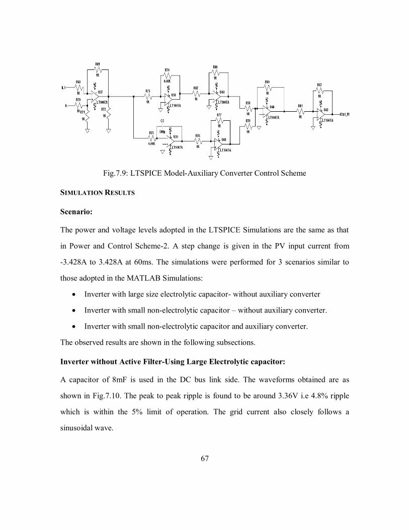
67
Fig.7.9: LTSPICE Model-Auxiliary Converter Control Scheme
SIMULATION RESULTS
Scenario:
The power and voltage levels adopted in the LTSPICE Simulations are the same as that
in Power and Control Scheme-2. A step change is given in the PV input current from
-3.428A to 3.428A at 60ms. The simulations were performed for 3 scenarios similar to
those adopted in the MATLAB Simulations:
Inverter with large size electrolytic capacitor- without auxiliary converter
Inverter with small non-electrolytic capacitor – without auxiliary converter.
Inverter with small non-electrolytic capacitor and auxiliary converter.
The observed results are shown in the following subsections.
Inverter without Active Filter-Using Large Electrolytic capacitor:
A capacitor of 8mF is used in the DC bus link side. The waveforms obtained are as
shown in Fig.7.10. The peak to peak ripple is found to be around 3.36V i.e 4.8% ripple
which is within the 5% limit of operation. The grid current also closely follows a
sinusoidal wave.

68
Fig.7.10: LTSPICE Output- Using Large Electrolytic Capacitor
Inverter without Active Filter-Using Small Non-Electrolytic Capacitor:
A capacitor of 1mF is used in the DC bus link side. The waveforms obtained are as
shown in Fig.7.11. The peak to peak ripple is found to be around 25.2V i.e 36% ripple
which is beyond the prescribed limitations. The grid current is also highly distorted.
Input current source
DC bus link capacitor voltage
Grid Current
69
Fig.7.11: LTSPICE Output - Using Small Non-Electrolytic Capacitor
Inverter with Active Filter-Using Small Non-Electrolytic Capacitor:
A capacitor of 1mF is used in the DC bus link side along with 850μF in the active power
decoupling circuit. The waveforms obtained are as shown in Fig.7.12. The peak to peak
ripple is found to be around 5V i.e 7.14% ripple which is pretty close to the defined limit
of operation. The grid current also closely follows a sinusoidal wave.
DC bus link capacitor voltage
Input current source
Grid current
70
Fig.7.12: LTSPICE Output- Using Active Power Decoupling Circuit
RECOMMENDED CAPACITORS
The different capacitors that could be considered for this specific application
complying with the expected voltage and ripple current ratings are specified in Table 7.1-
7.3. The tables discuss the aluminium electrolytic capacitor, ALC40 series, the
polypropylene metallized film capacitor,C4AE series and the CKH/CKE Lead
Aluminium electrolytic capacitors ratings [27]-[29].
Input current source
DC bus link capacitor
Grid current

71
Table 7.1: Aluminium Electrolytic Capacitor(ALC40) Ratings
Table 7.2: Polypropylene Metallized Film Capacitor(C4AE) Ratings
Capacitance(μF) ESR(mΩ) at
200C,100 Hz max
Impedance(mΩ) at
200C,10kHz(max)
Ripple Current(A)
at 1050C
Voltage = 450V 100Hz 10kHz
470 203 138 3.51 6.68
560 175 122 4.32 9.57
820 121 85 5.34 11.05
1200 105 71 5.84 11.64
1500 86 59 6.44 11.85
Capacitance
(μF)
dV/dt
(V/μs)
Ipkr(Apk) ESL(nH) ESR(mΩ)
700C at
10kHz
Irms(Arms)
700C at
10kHz
Rth
(0C/W)
Voltage = 450V
35 10 355 30 3.5 14 18
40 10 406 30 3.1 16 17
50 10 508 30 2.5 18 15
75 7 503 35 3.4 18 12
100 7 677 35 2.6 22 10
72
Capacitance(μF) ESR(mΩ) at 200C,
100Hz
Impedance(mΩ) at
200C, 100Hz
Ripple Current(A)
at 1050C
Voltage = 35V 100Hz 10kHz
1000 199 - 0.89 -
1500 154.8 - 1.14 -
2200 120.6 - 1.44 -
3900 202 166 1.87 2.09
5600 171 144 2.08 2.31
6800 145 120 2.55 2.84
8200 129 110 2.53 2.81
10,000 107 91 2.90 3.22
Table 7.3: Lead Aluminium Electrolytic Capacitor(CKH/CKE) Ratings

73
Chapter VIII: Conclusions and Future Scope
PROJECT SUMMARY AND RESULTS
This project discusses the implementation of a Grid-PV interface for transient
changes in the input power stage. The interface is basically a single-phase 3-level VSI.
The major issue that concerns the installation is the double frequency component that
arises at the bus link and prevents a clean and smooth DC from entering the inverter
input.
One of the earliest methods suggested is placing a large electrolytic capacitor at
the bus link, since it can handle very large ripple currents and is also cost-effective.
Nevertheless, the lifetime and reliability of the inverter reduces due to the electrolytic
capacitor. Thus, thin film capacitors were suggested as an alternate solution due to their
longevity. Despite this advantage, they turn out to be a very expensive solution.
In this project, an active power decoupling circuit has been proposed and
implemented in parallel with the bus link capacitor. The power decoupling circuit is
basically a bi-directional DC-DC converter with the configuration of the half-bridge
topology due to its high efficiency and ease of implementation. The converter acts as a
synchronous buck/boost operating in two modes based on power transfer within the
circuit. This auxiliary circuit compensates the output current of the bus link capacitor,
using typical PI control and nullifies it. The model has been simulated for two different
power and control schemes in the Grid-PV interface:
Control Scheme-1 uses a Type-II controller for regulating the bus link voltage in
the outer voltage loop and a PR controller for regulating the grid current in the
inner current loop.
Control Scheme-2 uses PI control in both the voltage and current control loops.
74
The effect of the increased excursions in the DC link voltage due to transient changes in
the input power stage is also resolved by using an active power decoupling circuit. This
significantly increases the bandwidth of operation without increasing the output current
distortion, playing a major role.
The amount of capacitance required for the DC bus link is drastically reduced
using this method under similar power and voltage levels as the electrolytic capacitor
method. In scheme-1, the amount of capacitance required has been found to reduce by
75.61% and in scheme-2, the capacitance is reduced by 77.5% , compared to a large
electrolytic capacitor.
The simulation studies have been performed using MATLAB Simulink and the
waveforms have been analyzed accordingly. The power decoupling method has been
found to keep the bus link capacitor voltage within the required 5% ripple limit
considered as per IEEE 1547 standards. In addition, the non-ideal characteristics of the
model have been studied by conducting electronic circuit simulation using LTSPICE and
the design was done appropriately. The observations complied with the results yielded by
MATLAB simulation.
FUTURE SCOPE
Complete closed loop control could be achieved by controlling the voltage across
the auxiliary storage capacitor and thus resisting excessive voltage levels in the storage
capacitor, and preventing dielectric breakdown.
75
Bibliography
[1] Fumihiro Shinjo, Keiji Wada and Toshihisa Shimizu, “A Single-Phase Grid-
Connected Inverter with a Power Decoupling Function,” in Power Electronics
Specialists Conference, 2007. PESC 2007. IEEE, 2007, pp. 1245–1249.
[2] D.C.Martins and R.Demonti, “Photovoltaic energy processing for utility
connected system,” IEEE IECON, vol. 2, pp. 1292-1296, 2001.
[3] T.Shimizu, M.Hirakata, T.Kamezawa and H.Watanabe, “Generation control
circuit for photovoltaic modules,” IEEE Trans. Power Electronics, vol. 16,No. 3,
pp. 293-300, 2001.
[4] Y.C.Kuo, T.J.Liang and J.F.Chen, “Novel maximum-power-point tracking
controller for photovoltaic energy conversion system,” IEEE Trans. Industrial
Electronics, vol. 48, no. 3, pp. 594-601, 2001.
[5] T.Shimizu, O.Hashimoto and G.Kimura, “A novel high-performance utility
interactive photovoltaic inverter system,” IEEE Trans. Power Electronics, vol. 18,
no. 2, pp. 704-711, 2003.
[6] Michael Salcone and Joe Bond, “Selecting Film Bus Link Capacitors for High
Performance Inverter Applications,” in Battery Conference on Applications and
Advances, 1999. The Fourteenth Annual, 1999, pp. 197–198.
[7] Soeren Baekhoj Kjaer, John.K.Pedersen and Blaabjerg, “A Review of Single
Phase Grid Connected Inverters for Photovoltaic Modules,” in Battery Conference
on Applications and Advances, 1999. The Fourteenth Annual, 1999, pp. 155–159.
[8] F.Blaabjerg, Chen Zhe, S.B.Kjaer, “Power electronics as efficient interface in
dispersed power generation systems,” IEEE Trans. Power Electronics, vol.19,
no.5, pp. 1184- 1194, Sept. 2004
[9] I.Serban and C.Marinescu, “Active power decoupling circuit for a single-phase
battery energy storage system dedicated to autonomous microgrids,” in
International Symposium on Industrial Electronics(ISIE), 2010, IEEE, 4-7 July
2010, pp. 2717-2722,
[10] T.Brekken, N.Bhiwapurkar, M.Rathi, N.Mohan, C.Henze and L.R.Moumneh,
“Utility-connected power converter for maximizing power transfer from a
photovoltaic source while drawing ripple-free current,” Power Electronics
Specialists Conference, 2002. pesc 02. 2002 IEEE 33rd Annual, 2002, vol.3, pp.
1518- 1522.
[11] B.K.Bose and D.Kastha, “Electrolytic capacitor elimination in power electronic
system by high frequency active filter,” Industry Applications Society Annual
Meeting, 1991., Conference Record of the 1991 IEEE ,1991, vol.1, pp. 869-878.

76
[12] Hirofumi Akagi, Akira Nabae and Satoshi Atoh, “Control Strategy of Active
Power Filters Using Multiple Voltage-Source PWM Converters,” IEEE Trans.
Industry Applications, vol.IA-22, no.3, pp. 460-465, May 1986.
[13] Gyu-Ha Choe, A.K.Wallace and Min-Ho Park, “Control technique of active
power filter for harmonic elimination and reactive power control,” Industry
Applications Society Annual Meeting, 1988., Conference Record of the 1988
IEEE , 2-7 Oct. 1988, vol.1, pp. 859-866.
[14] Fang Zheng Peng, “Application issues of active power filters," Industry
Applications Magazine, IEEE , vol.4, no.5, pp. 21-30, Sep/Oct 1998
[15] S.Z.Dai, N.Lujara and B.T.Ooi, “A unity power factor current-regulated SPWM
rectifier with a notch feedback for stabilization and active filtering,” IEEE
Trans.Power Electronics, vol.7, no.2, pp. 356-363, Apr 1992.
[16] T.Shimizu, K.Wada and N.Nakamura, “A flyback-type single phase utility
interactive inverter with low-frequency ripple current reduction on the DC input
for an AC photovoltaic module system,” Power Electronics Specialists
Conference, 2002. pesc 02. 2002 IEEE 33rd Annual , 2002, vol.3, pp. 1483- 1488.
[17] Yu Du, Xiaohu Zhou, Sanzhong Bai, S.Lukic and A.Huang, “Review of non-
isolated bi-directional DC-DC converters for plug-in hybrid electric vehicle
charge station application at municipal parking decks,” Applied Power
Electronics Conference and Exposition (APEC), 2010 Twenty-Fifth Annual IEEE,
21-25 Feb. 2010, pp. 1145-1151.
[18] Lisheng Shi, A.Meintz and M.Ferdowsi, “Single-phase bidirectional AC-DC
converters for plug-in hybrid electric vehicle applications,” Vehicle Power and
Propulsion Conference, 2008. VPPC '08. IEEE, 3-5 Sept. 2008, pp. 1-5.
[19] Yu Du, S.Lukic, B.Jacobson and A.Huang, “Review of high power isolated bi-
directional DC-DC converters for PHEV/EV DC charging infrastructure,” Energy
Conversion Congress and Exposition (ECCE), 2011 IEEE,17-22 Sept. 2011, pp.
553-560.
[20] P.T.Krein and R.S.Balog, “Cost-Effective Hundred-Year Life for Single-Phase
Inverters and Rectifiers in Solar and LED Lighting Applications Based on
Minimum Capacitance Requirements and a Ripple Power Port,” Applied Power
Electronics Conference and Exposition, 2009. APEC 2009. Twenty-Fourth
Annual IEEE, 15-19 Feb. 2009, pp. 620-625.
[21] N.A.Ninad and L.A.C.Lopes, “Operation of Single-phase Grid-Connected
Inverters with Large DC Bus Voltage Ripple,” Electrical Power Conference,
2007. EPC 2007. IEEE Canada, 25-26 Oct. 2007, pp. 172-176.
[22] Raja Ayyanar. (2011,May). Renewable Electric Energy Systems. Arizona State
University. Tempe, Arizona. [Lecture Notes].

77
[23] “International Rectifier® IRFZ44N HEXFET Power MOSFET.” [Online].
Available: http://www.irf.com/product-info/datasheets/data/irfz44n.pdf
[24] “Linear Technology® LT1716 Micropower, Precision Rail-to-Rail Comparator.”
[Online]. Available: http://cds.linear.com/docs/Datasheet/1716fa.pdf
[25] “Linear Technology® LT1007A Low-noise,High-Speed Precision Operational
Amplifiers.”[Online].Available:http://www.digchip.com/datasheets/parts/datashee
t/477/LT1007A.php
[26] “Electronics/Analog Multipliers.” [Online]. Available:
http://en.wikibooks.org/wiki/Electronics/Analog_multipliers
[27] “Kemet®
ALC40 Series, Aluminium Electrolytic Capacitors.” [Online].
Available:http://www.kemet.com/kemet/web/homepage/kechome.nsf/file/ALC40
%20Series/$file/F3304_ALC40.pdf
[28] “Kemet® C4AE Series , Polypropylene Film Capacitors.” [Online]. Available:
http://www.kemet.com/kemet/web/homepage/kechome.nsf/file/F3303_C4AE/$fil
e/F3303_C4AE.pdf
[29] "Illinois Capacitor,Inc® CKH/CKE Series, General Purpose Radial Lead
Aluminum Electrolytic Capacitors.” [Online]. Available:
http://www.illinoiscapacitor.com/pdf/ckh_cke.pdf
Related Documents