“Raisin Bun”-Type Composite Spheres of Silica and Semiconductor Nanocrystals Andrey L. Rogach, ²,‡ Dattatri Nagesha, ² John W. Ostrander, ² Michael Giersig, § and Nicholas A. Kotov* ,² Department of Chemistry, Oklahoma State University, Stillwater, Oklahoma 74078, Physico-Chemical Research Institute, Belarusian State University, 220050 Minsk, Belarus, and Hahn-Meitner-Institut, Abt. Physikalische Chemie, Glienickerstr. 100, D-15109, Berlin, Germany Received March 20, 2000. Revised Manuscript Received June 27, 2000 CdTe nanocrystals capped with 1-mercapto-2,3-propandiol, CdSe nanocrystals capped with sodium citrate, and core-shell CdSe/CdS nanocrystals capped with sodium citrate were synthesized in aqueous solutions, and their surface was modified by 3-mercaptopropyltri- methoxysilane (MPS) in water-ethanol mixtures. By addition of sodium silicate, “raisin bun”-type composite particles were formed, with either CdTe, CdSe, or CdSe/CdS nanocrystals being homogeneously incorporated as multiple cores into silica spheres of 40-80 nm size, accompanied by some alteration of optical properties of the nanoparticles and, in particular, the reduction of the luminescence quantum yield. Further, growth of larger silica spheres (100-700 nm) can be performed by the Sto ¨ber technique using either MPS-modified semiconductor nanocrystals or “raisin bun”-type composite particles as seeds, which gives semiconductor-doped silica globules of desirable sizes in the submicrometer range. The composite spheres can be used as building blocks for 3D colloidal crystals, prepared in this study for CdS/CdSe-doped 250 nm silica colloid. The shift of the photonic band gap to the red was observed in photonic crystals made of nanoparticles-doped silica due to the high refractive index of the semiconductors. Introduction Semiconductor nanocrystals prepared by wet chemical route are often considered for different applications, ranging from light-emitting diodes 1-4 to biological labels. 5-7 This interest arises from the possibility of tuning the optical properties of semiconductor nanoc- rystals by simply varying their size owing to the effect of quantum confinement. 8 The incorporation of metallic and semiconductor nanoparticles in the continuous solid films prepared by the sol-gel technique has led to inexpensive photonic materials partly already employed on the market or successfully tested with respect to numerous applications. 9 The new challenge in nano- particle-based materials and corresponding optoelec- tronic applications is their 2D and 3D organization on solid substrates. For nanocrystals taken as prepared, it was achieved by the Langmuir-Blodgett 10 or the layer-by-layer assembly techniques. 11 For nanoparticles * Corresponding author. E-mail: [email protected]. ² Oklahoma State University. ‡ Permanent address: Belarusian State University. § Hahn-Meitner-Institut. (1) Colvin, V. L.; Schlamp, M. C.; Alivisatos, A. P. Nature 1994, 370, 354. (2) Gao, M. Y.; Richter, B.; Kirstein, S.; Mo ¨hwald, H. J. Phys. Chem. B 1998, 102, 4096. (3) Mattoussi, H.; Radzilowski, L. H.; Dabbousi, B. O.; Thomas, E. L.; Bawendi, M. G.; Rubner, M. F. J. Appl. Phys. 1998, 83, 7965. (4) Gaponik, N. P.; Talapin, D. V.; Rogach, A. L. Phys. Chem. Chem. Phys. 1999, 1, 1787. (5) Bruchez, M.; Moronne, M.; Gin, P.; Weiss, S.; Alivisatos, A. P. Science 1998, 281, 2013. (6) Chan, W. C. W.; Nie, S. Science 1998, 281, 2016. (7) Mitchell, G. P.; Mirkin, C. A.; Letsinger, R. L. J. Am. Chem. Soc. 1999, 121, 8122. (8) Weller, H. Angew. Chem., Int. Ed. 1993, 32, 41; Alivisatos, A. P. J. Phys. Chem. 1996, 100, 13226. (9) Rottman, C.; Grader, G.; Hazan, Y. D.; Melchior, S.; Avnir, D. J. Am. Chem. Soc. 1999, 121, 8533-8543. Livage, J. Bull. Mater. Sci. 1999, 22, 201-205. Livage, J. Mater. Sci. Forum 1994, 152-153, 43- 54. Livage, J.; Sanchez, C. J. Non-Cryst. Solids 1992, 145, 11-19. Patra, A.; Sominska, E.; Ramesh, S.; Koltypin, Y.; Zhong, Z.; Minti, H.; Reisfeld, R.; Gedanken, A. J. Phys. Chem. B 1999, 103, 3361-3365. Reisfeld, R.; Panczer, G.; Patra, A.; Gaft, M. Mater. Lett. 1999, 38, 413- 417. Patra, A.; Reisfeld, R.; Minti, H. Mater. Lett. 1998, 37, 325-329. Lifshitz, E.; Dag, I.; Litvin, I.; Hodes, G.; Gorer, S.; Reisfeld, R.; Zelner, M.; Minti, H. Chem. Phys. Lett. 1998, 288, 188-196. Zelner, M.; Minti, H.; Reisfeld, R.; Cohen, H.; Tenne, R. Chem. Mater. 1997, 9, 2541- 2543. Zayat, M.; Einot, D.; Reisfeld, R. J. Sol-Gel Sci. Technol. 1997, 10, 67-74. Reisfeld, R. Adv. Sci. Technol. 1995, 11,3-13. Sorek, Y.; Reisfeld, R.; Finkelstein, I.; Ruschin, S. Opt. Mater. (Amsterdam) 1994, 4, 99-101. Reisfeld, R. Opt. Mater. (Amsterdam) 1994, 4,1-3. Sorek, Y.; Reisfeld, R.; Finkelstein, I.; Ruschin, S. Appl. Phys. Lett. 1993, 63, 3256-3258. Ptatschek, V.; Schreder, B.; Herz, K.; Hilbert, U.; Ossau, W.; Schottner, G.; Rahaeuser, O.; Bischof, T.; Lermann, G.; Materny, A.; Kiefer, W.; Bacher, G.; Forchel, A.; Su, D.; Giersig, M.; Mueller, G.; Spanhel, L. J. Phys. Chem. B 1997, 101, 8898-8906. Lembacher, C.; Schubert, U. New J. Chem. 1998, 22, 721-724. Kaiser, A.; Goersmann, A.; Schubert, U. J. Sol-Gel Sci. Technol. 1997, 8, 795- 799. Schubert, U. J. Chem. Soc., Dalton Trans. 1996, 3343-3348. Schubert, U.; Goersmann, C.; Schwertfeger, F.; Tewinkel, S. Polym. Mater. Sci. Eng. 1995, 73, 423-424. Schubert, U. New J. Chem. 1994, 18, 1049-1058. Schreder, B.; Schmidt, T.; Ptatschek, V.; Winkler, U.; Materny, A.; Umbach, E.; Lerch, M.; Mueller, G.; Kiefer, W.; Spanhel, L. J. Phys. Chem. B 2000, 104, 1677-1685. Leeb, J.; Gebhardt, V.; Mueller, G.; Haarer, D.; Su, D.; Giersig, M.; McMahon, G.; Spanhel, L. J. Phys. Chem. B 1999, 103, 7839-7845. Lorenz, C.; Emmerling, A.; Fricke, J.; Schmidt, T.; Hilgendorff, M.; Spanhel, L.; Muller, G. J. Non-Cryst. Solids 1998, 238,1-5. Spanhel, L.; Schmidt, H.; Uhrig, A.; Klingshirn, C. Mater. Res. Soc. Symp. Proc. 1992, 272, 53-58. Spanhel, L.; Arpac, E.; Schmidt, H. J. Non-Cryst. Solids 1992, 147- 148, 657-662. Spanhel, L.; Anderson, M. A. J. Am. Chem. Soc. 1991, 113, 2826-2833. 2676 Chem. Mater. 2000, 12, 2676-2685 10.1021/cm000244i CCC: $19.00 © 2000 American Chemical Society Published on Web 08/31/2000

Welcome message from author
This document is posted to help you gain knowledge. Please leave a comment to let me know what you think about it! Share it to your friends and learn new things together.
Transcript

“Raisin Bun”-Type Composite Spheres of Silica andSemiconductor Nanocrystals
Andrey L. Rogach,†,‡ Dattatri Nagesha,† John W. Ostrander,†Michael Giersig,§ and Nicholas A. Kotov*,†
Department of Chemistry, Oklahoma State University, Stillwater, Oklahoma 74078,Physico-Chemical Research Institute, Belarusian State University, 220050 Minsk, Belarus, and
Hahn-Meitner-Institut, Abt. Physikalische Chemie, Glienickerstr. 100,D-15109, Berlin, Germany
Received March 20, 2000. Revised Manuscript Received June 27, 2000
CdTe nanocrystals capped with 1-mercapto-2,3-propandiol, CdSe nanocrystals capped withsodium citrate, and core-shell CdSe/CdS nanocrystals capped with sodium citrate weresynthesized in aqueous solutions, and their surface was modified by 3-mercaptopropyltri-methoxysilane (MPS) in water-ethanol mixtures. By addition of sodium silicate, “raisinbun”-type composite particles were formed, with either CdTe, CdSe, or CdSe/CdS nanocrystalsbeing homogeneously incorporated as multiple cores into silica spheres of 40-80 nm size,accompanied by some alteration of optical properties of the nanoparticles and, in particular,the reduction of the luminescence quantum yield. Further, growth of larger silica spheres(100-700 nm) can be performed by the Stober technique using either MPS-modifiedsemiconductor nanocrystals or “raisin bun”-type composite particles as seeds, which givessemiconductor-doped silica globules of desirable sizes in the submicrometer range. Thecomposite spheres can be used as building blocks for 3D colloidal crystals, prepared in thisstudy for CdS/CdSe-doped 250 nm silica colloid. The shift of the photonic band gap to thered was observed in photonic crystals made of nanoparticles-doped silica due to the highrefractive index of the semiconductors.
Introduction
Semiconductor nanocrystals prepared by wet chemicalroute are often considered for different applications,ranging from light-emitting diodes1-4 to biologicallabels.5-7 This interest arises from the possibility oftuning the optical properties of semiconductor nanoc-rystals by simply varying their size owing to the effectof quantum confinement.8 The incorporation of metallicand semiconductor nanoparticles in the continuous solidfilms prepared by the sol-gel technique has led toinexpensive photonic materials partly already employedon the market or successfully tested with respect tonumerous applications.9 The new challenge in nano-particle-based materials and corresponding optoelec-tronic applications is their 2D and 3D organization on
solid substrates. For nanocrystals taken as prepared,it was achieved by the Langmuir-Blodgett10 or thelayer-by-layer assembly techniques.11 For nanoparticles
* Corresponding author. E-mail: [email protected].† Oklahoma State University.‡ Permanent address: Belarusian State University.§ Hahn-Meitner-Institut.(1) Colvin, V. L.; Schlamp, M. C.; Alivisatos, A. P. Nature 1994,
370, 354.(2) Gao, M. Y.; Richter, B.; Kirstein, S.; Mohwald, H. J. Phys. Chem.
B 1998, 102, 4096.(3) Mattoussi, H.; Radzilowski, L. H.; Dabbousi, B. O.; Thomas, E.
L.; Bawendi, M. G.; Rubner, M. F. J. Appl. Phys. 1998, 83, 7965.(4) Gaponik, N. P.; Talapin, D. V.; Rogach, A. L. Phys. Chem. Chem.
Phys. 1999, 1, 1787.(5) Bruchez, M.; Moronne, M.; Gin, P.; Weiss, S.; Alivisatos, A. P.
Science 1998, 281, 2013.(6) Chan, W. C. W.; Nie, S. Science 1998, 281, 2016.(7) Mitchell, G. P.; Mirkin, C. A.; Letsinger, R. L. J. Am. Chem.
Soc. 1999, 121, 8122.(8) Weller, H. Angew. Chem., Int. Ed. 1993, 32, 41; Alivisatos, A.
P. J. Phys. Chem. 1996, 100, 13226.
(9) Rottman, C.; Grader, G.; Hazan, Y. D.; Melchior, S.; Avnir, D.J. Am. Chem. Soc. 1999, 121, 8533-8543. Livage, J. Bull. Mater. Sci.1999, 22, 201-205. Livage, J. Mater. Sci. Forum 1994, 152-153, 43-54. Livage, J.; Sanchez, C. J. Non-Cryst. Solids 1992, 145, 11-19.Patra, A.; Sominska, E.; Ramesh, S.; Koltypin, Y.; Zhong, Z.; Minti,H.; Reisfeld, R.; Gedanken, A. J. Phys. Chem. B 1999, 103, 3361-3365.Reisfeld, R.; Panczer, G.; Patra, A.; Gaft, M. Mater. Lett. 1999, 38, 413-417. Patra, A.; Reisfeld, R.; Minti, H. Mater. Lett. 1998, 37, 325-329.Lifshitz, E.; Dag, I.; Litvin, I.; Hodes, G.; Gorer, S.; Reisfeld, R.; Zelner,M.; Minti, H. Chem. Phys. Lett. 1998, 288, 188-196. Zelner, M.; Minti,H.; Reisfeld, R.; Cohen, H.; Tenne, R. Chem. Mater. 1997, 9, 2541-2543. Zayat, M.; Einot, D.; Reisfeld, R. J. Sol-Gel Sci. Technol. 1997,10, 67-74. Reisfeld, R. Adv. Sci. Technol. 1995, 11, 3-13. Sorek, Y.;Reisfeld, R.; Finkelstein, I.; Ruschin, S. Opt. Mater. (Amsterdam) 1994,4, 99-101. Reisfeld, R. Opt. Mater. (Amsterdam) 1994, 4, 1-3. Sorek,Y.; Reisfeld, R.; Finkelstein, I.; Ruschin, S. Appl. Phys. Lett. 1993, 63,3256-3258. Ptatschek, V.; Schreder, B.; Herz, K.; Hilbert, U.; Ossau,W.; Schottner, G.; Rahaeuser, O.; Bischof, T.; Lermann, G.; Materny,A.; Kiefer, W.; Bacher, G.; Forchel, A.; Su, D.; Giersig, M.; Mueller,G.; Spanhel, L. J. Phys. Chem. B 1997, 101, 8898-8906. Lembacher,C.; Schubert, U. New J. Chem. 1998, 22, 721-724. Kaiser, A.;Goersmann, A.; Schubert, U. J. Sol-Gel Sci. Technol. 1997, 8, 795-799. Schubert, U. J. Chem. Soc., Dalton Trans. 1996, 3343-3348.Schubert, U.; Goersmann, C.; Schwertfeger, F.; Tewinkel, S. Polym.Mater. Sci. Eng. 1995, 73, 423-424. Schubert, U. New J. Chem. 1994,18, 1049-1058. Schreder, B.; Schmidt, T.; Ptatschek, V.; Winkler, U.;Materny, A.; Umbach, E.; Lerch, M.; Mueller, G.; Kiefer, W.; Spanhel,L. J. Phys. Chem. B 2000, 104, 1677-1685. Leeb, J.; Gebhardt, V.;Mueller, G.; Haarer, D.; Su, D.; Giersig, M.; McMahon, G.; Spanhel,L. J. Phys. Chem. B 1999, 103, 7839-7845. Lorenz, C.; Emmerling,A.; Fricke, J.; Schmidt, T.; Hilgendorff, M.; Spanhel, L.; Muller, G. J.Non-Cryst. Solids 1998, 238, 1-5. Spanhel, L.; Schmidt, H.; Uhrig,A.; Klingshirn, C. Mater. Res. Soc. Symp. Proc. 1992, 272, 53-58.Spanhel, L.; Arpac, E.; Schmidt, H. J. Non-Cryst. Solids 1992, 147-148, 657-662. Spanhel, L.; Anderson, M. A. J. Am. Chem. Soc. 1991,113, 2826-2833.
2676 Chem. Mater. 2000, 12, 2676-2685
10.1021/cm000244i CCC: $19.00 © 2000 American Chemical SocietyPublished on Web 08/31/2000
coated with silica, both the stability of the semiconduc-tor core can be increased and a different periodicity ofthe nanoparticles arrangement can be obtained. Ad-ditionally, the silica surface can be easily modified withdifferent groups to facilitate the solubility of spheres indifferent solvents and to control their interaction withsubstrate. While still pursuing other means of nano-particles organization,10,11 we focused this study onsilica/semiconductor composite particles and synthesisof subsequent organization of quantum dots in theperiodic crystalline structure with periodicity compa-rable to the wavelength of visible light.
An Individual coating of single nanoparticles withsilica has been successfully realized for a variety ofmetal particles,12-14 yielding silica spheres of the desiredsizes containing a single metal core placed precisely attheir centers. Coating of small 4-10 nm single semi-conductor nanocrystals with silica has been realized andhas been shown to suppress the photochemical degrada-tion of the nanoparticles.5,15 On the other hand, dopingof 50-1000 nm uniformly sized silica colloids withluminescent semiconductor nanocrystals has not yetbeen realized. Optically active SiO2 colloids can serveas the starting point for a variety of photonic materialssuch as laser media, diffraction gratings, and sensingfilms. As well, such particles are needed for the inves-tigation of fundamental particle-particle interactionsin fluid media, which despite a quite long history,continue to surprise the researchers.16 In this respect,the silica spheres doped with luminescent semiconduc-tor nanoparticles can be used for monitoring of the
colloidal motion in solution by confocal microscopy.Currently, luminescence tagging is usually achieved byincorporating dyes in the colloidal particles,17 whichundergo fast photobleaching.
A large class of photonic materials is based onmonodisperse silicasthe so-called artificial opals. Theyare attracting much attention recently due to theirunique optical properties and their causative similarityto the electrical properties of solids.18-27 Colloidalcrystals prepared by the self-organization of monodis-perse latex28,29 or silica28,23-25,30-32 spheres have beenshown to possess a photonic pseudogap and, therefore,are considered as promising prototypes for 3D photoniccrystals (“optical semiconductors”) in the visible andnear-IR parts of the electromagnetic spectrum. Thesefindings have stimulated extensive studies of thestructural22,24,27,30-33 and optical22,24,30,32 properties ofcolloidal crystals, their use as templates for fabricatinghigh-refractive index 3D replicas,34 and the spontaneousemission of dye molecules35 and semiconductor nano-crystals36-39 embedded into the voids of colloidal crys-
(10) Kotov, N. A.; Meldrum, F. C.; Fendler, J. H. J. Phys. Chem.1994, 98, 8827. Kotov, N. A.; Meldrum, F. C.; Wu, C.; Fendler, J. H. J.Phys. Chem. 1994, 98, 2735-2738. Meldrum, F. C.; Kotov, N. A.;Fendler, J. H.; Langmuir 1994, 10, 2035-2040. Meldrum, F. C.; Kotov,N. A.; Fendler, J. H. Chem. Mater. 1995, 7, 1112-1116. Meldrum, F.C.; Kotov, N. A.; Fendler, J. H. J. Chem. Soc., Faraday Trans. 1995,91 (4), 673-680. Markovich, G.; Collier, C. P.; Heath, J. R. Phys. Rev.Lett. 1998, 80, 3807-3810. Medeiros-Ribeiro, G.; Ohlberg, D. A. A.;Williams, R. S.; Heath, J. R. Phys. Rev. B: Condens. Matter Mater.Phys. 1999, 59, 1633-1636. Henrichs, S. E.; Sample, J. L.; Shiang, J.J.; Heath, J. R.; Collier, C. P.; Saykally, R. J. J. Phys. Chem. B 1999,103, 3524-3528. Weitz, I. S.; Sample, J. L.; Ries, R.; Spain, E. M.;Heath, J. R. J. Phys. Chem. B 2000, 104, 4288-4291. Dabbousi, B.O.; Murray, C. B.; Rubner, M. F.; Bawendi, M. G. Chem. Mater. 1994,6, 216-219. Fendler, J. H. Chem. Mater. 1996, 8, 1616-1624. Li, L.S.; Hui, Z.; Chen, Y.; Zhang, X. T.; Peng, X.; Liu, Z.; Li, T. J. J. ColloidInterface Sci. 1997, 192, 275-280.
(11) Kotov, N. A.; Fendler, J. H.; Dekany, I. J. Phys. Chem. 1995,99, 13065. Aliev, F.; Correa-Duarte, M. A.; Mamedov, A.; Ostrander,J. W.; Giersig, M. Liz-Marzan, L. M.; Kotov, N. A. Adv. Mater. 1999,11 (12), 1006-1010. Mamedov, A.; Ostrander, J. W.; Aliev, F.; Kotov,N. A. Langmuir 2000, 16 (8), 3941-3949. Pastoriza-Santos, I.; Koktysh,D. S.; Mamedov, A. A.; Giersig, M.; Kotov, N. A.; Liz-Marzan, L. M.Langmuir 2000, 16 (6), 2731-2735. Mamedov, A.; Kotov, N. A.Langmuir 2000, 16, 5530. Rogach, A.; Koktysh, D.; Harrison, M.; Kotov,N. A. Chem. Mater. 2000, 12, 1526. Liu, Y. J.; Wang, A. B.; Claus, R.O. Appl. Phys. Lett. 1997, 71, 2265-2267. Lvov, Y.; Ariga, K.; Onda,M.; Ichinose, I.; Kunitake, T. Langmuir 1997, 13, 6195-6203. Caruso,F.; Lichtenfeld, H.; Giersig, M.; Mohwald, H. J. Am. Chem. Soc. 1998,120, 8523-8524. Decher, G.; Schmitt, J.; Brand, F.; Lehr, B.; Oeser,R.; Losche, M.; Bouwman, W.; Kjaer, K.; Calvert, J.; Geer, R.; Dressik,W.; Shashidhar, R. Adv. Mater. 1998, 10, 338. Gao, M. Y.; Richter, B.;Kirstein, S.; Mohwald, H. J. Phys. Chem. B 1998, 102, 4096. Gao, M.Y.; Kirstein, S.; Rogach, A. L.; Weller, H.; Mohwald, H. Adv. Sci.Technol. (Faenza, Italy) 1999, 27, 347.
(12) (a) Liz-Marzan, L. M.; Giersig, M.; Mulvaney, P. Chem.Commun. 1996, 731. (b) Buining, P. A.; Liz-Marzan, L. M.; Philipse,A. P. J. Colloid Interface Sci. 1996, 179, 318.
(13) Liz-Marzan, L. M.; Giersig, M.; Mulvaney, P. Langmuir 1996,12, 4329.
(14) Ung, T.; Liz-Marzan, L. M.; Mulvaney, P. Langmuir 1998, 14,3740.
(15) Correa-Duarte, M. A.; Giersig, M.; Liz-Marzan, L. M. Chem.Phys. Lett. 1998, 286, 497.
(16) Aranda-Espinoza, H.; Chen, Yi.; Dan, N.; Lubensky, T. C.;Nelson, P.; Ramos, L.; Weitz, D. A. Science 1999, 285, 394. Ramos, L.;Lubensky, T. C.; Dan, N.; Nelson, P.; Weitz, D. A. Science 1999, 286,2325. Wei, Q.-H.; Bechinger, C.; Leiderer, P. Science 1999, 287, 625.Weeks, E. R.; Crocker, J. C.; Levitt, A. C.; Schofield, A.; Weitz, D. A.Science 1999, 287, 627.
(17) Char, K.; Frank, C. W.; Gast, A. P. Langmuir 1990, 6, 767.Koppel, D. E.; Morgan, F.; Cowan, A. E.; Carson, J. H. Biophys. J.1994, 66, 502. Lowe, C. P.; Frenkel, D. Phys. Rev. E 1996, 54, 2704.
(18) Jiang, P.; Bertone, J. F.; Hwang, K. S.; Colvin, V. L. Chem.Mater. 1999, 11, 2132.
(19) Tarhan, I. I.; Watson, H. Phys. Rev. Lett. 1996, 76, 315.(20) Vos, W. L.; Sprik, R.; van Blaaderen, A.; Imhof, A.; Lagendijk,
A.; Wegdam, G. H. Phys. Rev. B 1996, 53, 16231.(21) Astratov, V. N.; Vlasov, Yu. A.; Karimov, O. Z.; Kaplyanskii,
A. A.; Musikhin, Yu. G.; Bert, N. A.; Bogomolov, V. N.; Prokofiev, A.V. Phys. Lett. A 1996, 222, 349.
(22) Bogomolov, V. N.; Gaponenko, S. V.; Germanenko I. N.;Kapitonov, A. M.; Petrov, E. P.; Gaponenko, N. V.; Prokofiev, A. V.;Ponyavina, A. N.; Silvanovich, N. I.; Samoilovich, S. M. Phys. Rev. E1997, 55, 7619.
(23) Van Blaaderen, A.; Ruel, R.; Wiltzius, P. Nature 1997, 385,321.
(24) Miguez, H.; Lopez, C.; Meseguer, F.; Blanco, A.; Vazquez, L.;Mayoral, R.; Ocana, M.; Fornes, V.; Mifsud, A. Appl. Phys. Lett. 1997,71, 1148.
(25) Van Blaaderen, A. Science 1998, 282, 887.(26) Romanov, S. G.; Fokin, A. V.; de la Rue, R. M. J. Phys. C 1999,
11, 3593.(27) Rogach, O. E.; Kornowski, A.; Kapitonov, A. M.; Gaponenko,
N. V.; Gaponenko, S. V.; Eychmuller, A.; Rogach, A. L. Mater. Sci. Eng.B 1999, 64, 64.
(28) Pieranski, P. Contemp. Phys. 1983, 24, 25.(29) Clark, N. A.; Hurd, A. J.; Ackerson, B. J. Nature 1979, 281,
57. Tarhan, I. I.; Zunkin, M. P.; Watson, G. H. Opt. Lett. 1995, 20,1571. Fujimura, T.; Edamatsu, K.; Itoh, T.; Shimada, R.; Imada, A.;Koda, T.; Chiba, N.; Muramatsu, H.; Ataka, T. Opt. Lett. 1997, 22,489. Park, S. H.; Gates, B.; Xia, Y. Adv. Mater. 1999, 11, 462. Gates,B.; Qin, D.; Xia, Y. Adv. Mater. 1999, 11, 466.
(30) Jiang, P.; Hwang, K. S.; Mittleman, D. M.; Bertone, J. F.;Colvin, V. L. J. Am. Chem. Soc. 1999, 121, 11630-11637. Jiang, P.;Cizeron, J.; Bertone, J. F.; Colvin, V. L. J. Am. Chem. Soc. 1999, 121,7957-7958. Tsunekawa, S.; Barnakov, Y.; Poborchii, V. V.; Samoilov-ich, S. M.; Kasuya, A.; Nishina, Y. Microporous Mater. 1997, 8, 275-282. Hayward, R. C.; Saville, A.; Aksay, A. Nature (London) 2000, 404,56-59.
(31) Mayoral, R.; Requena, J.; Moya, J. S.; Lopez, C.; Cintas, A.;Miguez, H.; Meseguer, F.; Vazkuez, L.; Holgado, M.; Blanco, A. Adv.Mater. 1997, 9, 257. Miguez, H.; Meseguer, F.; Lopez, C.; Mifsud, A.;Moya, J. S.; Vazquez, L. Langmuir 1997, 13, 6009.
(32) Bogomolov, V. N.; Gaponenko, S. V.; Kapitonov, A. M.; Prokofiev,A. V.; Ponyavina, A. N.; Silvanovich, N. I.; Samoilovich, S. M. Appl.Phys. A 1996, 63, 613. Miguez, H.; Meseguer, F.; Lopez, C.; Blanko,A.; Moya, J. S.; Requena, J.; Mifsud, A.; Fornes, V. Adv. Mater. 1998,10, 480. Vlasov, Yu. A.; Astratov, V. N.; Karimov, O. Z.; Kaplyanskii,A. A.; Bogomolov, V. N.; Prokofiev, A. V. Phys. Rev. B, 1997, 55, 13357.
(33) Megens, M.; van Kats, C. M.; Bosecke, P.; Vos, W. L. J. Appl.Crystallogr. 1997, 30, 637. Vos, W. L.; Megens, M.; van Kats, C. M.;Bosecke, P. Langmiur 1997, 13, 6004.
“Rasin Bun”-Type Composite Spheres Chem. Mater., Vol. 12, No. 9, 2000 2677
tals. Because of the substantial difference between theelectron and photon wavelengths, the electron andphoton densities of states can be engineered separatelywithin the same mesoscopic structure, which can berealized in colloidal photonic crystals doped with lumi-nescent semiconductor nanocrystals.36-39 The interplayof electron and photon confinement opens the pathwayto novel light sources with controllable spontaneousemission.
In this paper, we report the synthesis of “raisin-bun”-type submicrometer-size composite spheres of silicalabeled with different semiconductor nanocrystals: thiol-capped CdTe nanoparticles, citrate-stabilized CdSenanoparticles, and citrate-stabilized core-shell CdSe/CdS nanocrystals. The optical properties of photoniccrystal with quantum dots positioned inside silicaspheres are principally different from the approachesreported in refs 36-39, where nanocrystals were infil-trated in voids. Besides the protection from oxidation,embedding the nanoparticles in the core of the colloidhas significant advantage over adsorbing the nanopar-ticles on the surface,40 because this does not alterparticle-particle interactions and affords further func-tionalization of silica. The isolation of the nanoparticlesinside the spheres allows for decoupling of the mediaeffects on photonic band gap and media effects on theluminescence intensity of quantum dots, which willinterfere otherwise. This feature combined with thecontrollable diameter of silica spheres and the variableemission of spectrum of nanoparticles makes possiblethe comprehensive study of the interplay between thephotonic and electronic characteristics. We successfullyrealized the encapsulation of spatially separated quan-tum dots inside the silica spheres. However, the simul-taneous decrease of the luminescence quantum yieldwas observed for all nanoparticles used in this study.This problem is quite important in the context ofpossible photonic applications and will require furtherexperimental work. On the other hand, the incorpora-
tion of the nanocrystals altered the photonic band gapof the colloidal crystal, which demonstrated the pos-sibility of the band gap tuning independently of thesilica sphere diameter and void medium.
Experimental Section
For the preparation of composite silica structures, sodiumsilicate solution (27 wt % SiO2, Fisher Scientific), 3-mercap-topropyltrimethoxysilane (MPS, Fluka), tetraethoxysilane(TEOS, 98%, Fluka), and pure grade ethanol were used asreceived. Milli-Q-deionized water was used for all the prepara-tions.
Aqueous solutions of CdTe nanocrystals capped with 1-mer-capto-2,3-propandiol (thioglycerol) were prepared by the methodof Rogach et al. reported previously.41 Briefly, 22 mL of freshlyprepared oxygen-free 0.05 M NaHTe solution was added to125 mL of a 0.013 M nitrogen-saturated Cd(ClO4)2‚6H2Oaqueous solution at pH 11.2 in the presence of 0.5 mL of1-thioglycerol as a stabilizing agent. The solution was heatedto 96 °C and refluxed for as long as 48 h to promote the growthof CdTe nanocrystals. Fractions of CdTe nanoparticles ofdifferent sizes were taken from the crude solution at differentreflux times, precipitated by 2-propanol, redissolved in purewater again at pH 9.0, and used for preparation of compositestructures.
Citrate-stabilized CdSe nanocrystals were prepared accord-ing to the following procedure: To 45 mL of water were added0.05 g sodium citrate and 2 mL of 4 × 10⁻² M cadmiumperchlorate and the pH was adjusted to 9.0 by 0.1 M NaOH.The solution was bubbled with nitrogen for 10 min, 2 mL of 1× 10⁻² M N,N-dimethylselenourea was added, and the mixturewas heated in a conventional 900 W (Sharp) microwave ovenfor 50 s. The final volume of the solution after heating was ca.40 mL. In the recipe described above, the Cd:Se molar ratiowas 4:1, which leads to CdSe nanoparticles with ca. 4.0 nmdiameter; by increasing the Cd concentration it is possible tosynthesize smaller CdSe nanocrystals.
For the preparation of core-shell CdSe/CdS nanocrystals,citrate-stabilized CdSe nanoparticles synthesized in aqueoussolution as described above (Cd:Se molar ratio 4:1) were usedas the initial material with thioacetamide as a sulfur source.To a given volume of CdSe nanoparticle solution as preparedwas added a 4 × 10⁻² M solution of thioacetamide in a quantitythat the molar ratio of Sadded:Seinitial was 1:1. The mixture washeated in the sealed round-bottom flask in a silicon oil bathat 70-80 °C for up to 24 h.
Composite structures of silica and semiconductor nanocrys-tals were prepared by the modified method of ref 15. First, asolution of 2 µL of MPS in 80 mL of ethanol was added undervigorous stirring to 20 mL of aqueous solutions of CdTe, CdSe,or CdSe/CdS nanocrystals with a nanoparticle concentrationof 0.5 and 1.5 mM referred to Cd for CdTe and CdSe/CdSnanoparticles, respectively. The mixtures were stirred for ca.12 h and then 0.4 mL of 0.54 wt % solution of sodium silicatewas added to 40 mL of these solutions. The addition of silicateresulted in a pH increase from 8.5 to 10.7. The mixtures wereallowed to react for about 4 h under UV-vis control and thenripened for 5 days.
Silica spheres doped with semiconductor nanocrystals wereprepared by the modified Stober synthesis42 using ethanol-water mixtures of either MPS-modified semiconductor nanoc-rystals or “raisin bun”-type composite particles as growthseeds.
Colloidal crystals were made by slow natural sedimentationof charge-stabilized nanocrystal-doped silica spheres fromDMF, followed by evaporation of the solvent.27
(34) Norris, D. J. Adv. Mater. 1999, 11, 165. Park, S. H.; Xia, Y.Adv. Mater. 1998, 10, 1045. Park, S. H.; Xia, Y. Chem. Mater. 1998,10, 1745. Holland, B. T.; Blanford, C. F.; Stein, A. Science 1998, 281,538. Wijnhoven, J. E. G. J.; Vos, W. L. Science 1998, 281, 802.Zakhidov, A. A.; Baughman, R. H.; Iqbal, Z.; Cui, C.; Khayrullin, I.;Dantas, S. O.; Marti, J.; Ralchenko, V. G. Science 1998, 282, 897.Kapitonov, A. M.; Gaponenko, N. V.; Bogomolov, V. N.; Prokofiev, A.V.; Samoilovich, S. M.; Gaponenko, S. V. Phys. Stat. Solidi (a) 1998,165, 119. Vlasov, Yu. A.; Yao, N.; Norris, D. J. Adv. Mater. 1999, 11,165.
(35) Petrov, E. P.; Bogomolov, V. N.; Kalosha, I. I.; Gaponenko, S.V. Phys. Rev. Lett. 1998, 81, 77. Yamasaki, T.; Tsutsui, T. Appl. Phys.Lett. 1998, 72, 1957. Yoshino, K.; Tada, K.; Ozaki, M.; Zakhidov, A.A.; Baughman, R. H. Appl. Phys. Lett. 1998, 73, 3506.
(36) Vlasov, Yu. A.; Luterova, K.; Pelant, I.; Honerlage, B.; Astratov,V. N. Appl. Phys. Lett. 1997, 71, 1616. Astratov, V. N.; Bogomolov, V.N.; Kaplyanskii, A. A.; Prokofiev, A. V.; Samoilovich, L. A.; Samoilovich,S. M.; Vlasov, Yu. A. Nuovo Cimento D 1995, 17, 1349. Vlasov, Yu. A.;Yao, N.; Norris, D. J. Adv. Mater. 1999, 11, 165.
(37) Blanco, A.; Lopez, C.; Mayoral, R.; Meseguer, F.; Mifsud, A.;Herrero, J. Appl. Phys. Lett. 1998, 73, 1781. Miguez, H.; Blanco, A.;Lopez, C.; Meseguer, F.; Yates, H. M.; Pemble, M. E.; Lopez-Tejeira,F.; Garcia-Vidal, F. J.; Sanchez-Dehesa, J. J. Lightwave Techn. 1999,17, 1975.
(38) Romanov, S. G.; Fokin, A. V.; Alperovich, V. I.; Johnson, N.P.; De La Rue, R. M. Phys. Stat. Solidi (a) 1997, 164, 169.
(39) Gaponenko, S. V.; Kapitonov, A. M.; Bogomolov, V. N.; Prokofiev,A. V.; Eychmuller, A.; Rogach, A. L. JETP Lett. 1998, 68, 142.
(40) Susha, A. S.; Caruso, F.; Rogach, A. L.; Sukhorukov, G. B.;Kornowski, A.; Mohwald, H.; Giersig, M.; Eychmuller, A.; Weller, H.Colloid. Surf. A 2000, 163, 39. Megens, M.; Wijnhoven, J. E. G. J.;Lagendijk, A.; Vos, W. L. J. Opt. Soc. Am. B 1999, 16, 1403. Megens,M.; Wijnhoven, J. E. G. J.; Lagendijk, A.; Vos, W. L. Phys. Rev. A 1999,59, 4727.
(41) Rogach, A. L.; Katsikas, L.; Kornowski, A.; Su, D.; Eychmuller,A.; Weller, H. Ber. Bunsen-Ges. Phys. Chem. 1996, 100, 1772; 1997,101, 1668.
(42) Stober, W.; Fink, A.; Bohn, E. J. Colloid Interface Sci. 1968,26, 62.
2678 Chem. Mater., Vol. 12, No. 9, 2000 Rogach et al.

UV-vis absorption spectra were taken on a HP8453 diodearray Hewlett-Packard spectrophotometer. Photoluminescencespectra were measured on a modular Fluorolog 3 SPEXspectrofluorimeter. Transmission electron microscopy (TEM)images were taken on a Philips CM12 microscope operatingat an acceleration voltage of 120 kV and on a Philips CM200FEG microscope operating at an acceleration voltage of 200kV. High-resolution TEM images were digitally recorded witha CCD camera. Samples were prepared by evaporation of adrop of colloidal solution on a carbon-coated copper grid.Scanning electron microscopy (SEM) pictures were made witha JSM 6400 microscope.
Results
Preparation of Nanocrystals. Thioglycerol-cappedCdTe nanoparticles show a peak corresponding to 1s-1s electronic transitions in the absorption spectra(Figure 1a) and a pronounced, relatively narrow (fwhm) 35-50 nm) “excitonic” luminescence (5% room-tem-perature quantum efficiency as measured in comparisonwith Rhodamine 6G), which is tunable with particle size
due to the quantum confinement effect (Figure 1b).There is also a weak luminescence band originatingfrom the emission from trap sites43 that is strongly red-shifted from the absorption onset and is more pro-nounced in smaller CdTe nanoparticles. Particles growcontinuously during the prolonged refluxing from ca. 2.5to 5.0 nm. It is envisaged that thiols slowly decomposedduring reflux and serve as a sulfide source, so theformation of mixed and core-shell CdTe/CdS crystalsparticles is likely for advanced stages of heating.44
Citrate-stabilized CdSe nanocrystals also show well-defined 1s-1s electronic transitions in the absorptionspectra (Figure 2a), excitonic emission that are tunablewith particle size in the visible spectral region, albeitnot to such an extent as for thiol-capped CdTe nanoc-rystals, and relatively strong trapped emission (Figure2b). The room-temperature excitonic emission of CdSe
(43) Kapitonov, A. M.; Stupak, A. P.; Gaponenko, S. V.; Petrov, E.P.; Rogach, A. L.; Eychmuller, A. J. Phys. Chem. B 1999, 103, 10109.
(44) Rogach, A. L. Mater. Sci. Eng. B, 2000, 69, 435.
Figure 1. Absorption (a) and luminescence (b) spectra ofthioglycerol-capped CdTe nanocrystals of different sizes (2.5-5.0 nm) in aqueous solutions.
Figure 2. Absorption (a) and luminescence (b) spectra ofcitrate-stabilized CdSe nanocrystals of different sizes (3.0-5.0 nm) in aqueous solutions.
“Rasin Bun”-Type Composite Spheres Chem. Mater., Vol. 12, No. 9, 2000 2679

nanoparticles is weak, ca. 0.1-0.15% in comparison withRhodamine 6G. However, the useful feature of nano-particles synthesized with citrate is the combination ofa relatively narrow size distribution and lability of thestabilizer, which is beneficial for many reactions ofsurface modification. The quantum efficiency of theexcitonic luminescence can be sufficiently enhanced bycapping the surface of the nanocrystals with a higherband gap inorganic layer. These ”core/shell” compositematerials show sufficiently higher luminescence quan-tum yield than “bare” nanoparticles due to improvedpassivation of the surface. Examples of such core/shellstructures include CdSe/ZnSe,45 CdSe/ZnS,46,47 andCdSe/CdS48 nanoparticles synthesized by the TOP/TOPO method, with reports of room-temperature quan-tum efficiencies of up to 50% for the CdSe/CdS mate-rial.48 It was therefore decided to overcoat our CdSenanocrystals with a layer of CdS in order to obtain amaterial with higher luminescence quantum yield.Thioacetamide was chosen as a sulfur source as it cangradually liberate sulfide ions in aqueous solution,which slowly react with excess of Cd2+ in the CdSecolloidal solution.49
In the course of the preparation of the core-shellparticles, both absorption and luminescent spectra ofCdSe undergo some change as compared to mere heat-ing without the sulfur source (Figure 3). The heatinginduces a slight growth of CdSe nanocrystals that isaccompanied by the red shift of the absorption edge andexcitonic luminescence band (compare Figures 2 and 3).For CdSe/CdS nanoparticles, absorbance increases atall wavelengths, and the absorption edge shifts 3-4 nmto the red. The luminescence maximum of excitonicband shifts correspondingly by 4-5 nm to the red, andthe relative intensity of trapped emission decreases,while its maximum shifts by 20 nm to the blue. Theluminescence intensity grows up drasticallys20-30timessand the quantum yield reaches 4.2%. Note thatthe luminescence intensity of bare CdSe particles, whenheated, increases as well; however, the quantum yieldin this case never exceeded 0.5-0.8%. This indicates theformation of CdS shells on CdSe cores, which passivatesCdSe surface defects and leads to the localization ofphotoexcited charge carriers in the CdSe core. Cor-respondingly, the trapped emission of bare CdSe nano-particles is strongly depressed for the CdSe/CdS core-shells, whereas the relative intensity of trapped emissionof bare CdSe nanoparticles increases during heating.Note that the presence of the epitaxially deposited CdSshell cannot be seen in the TEM images even at thehighest resolution, because the crystal structures ofhexagonal CdS and CdSe are very close, and therefore,one has to limit the probing of the core-shell structuresto spectroscopic means.
Silication of the Nanocrystals. CdTe nanocrystalscapped with thioglycerol, CdSe nanocrystals capped
with sodium citrate, and core-shell CdSe/CdS nanoc-rystals capped with sodium citrate were used for thepreparation of composite structures with silica. Theaverage size of the nanoparticles used was 3.0, 4.0, and5.0 nm for CdTe, CdSe, and CdSe/CdS, respectively,with ca. 15% polydispersity.
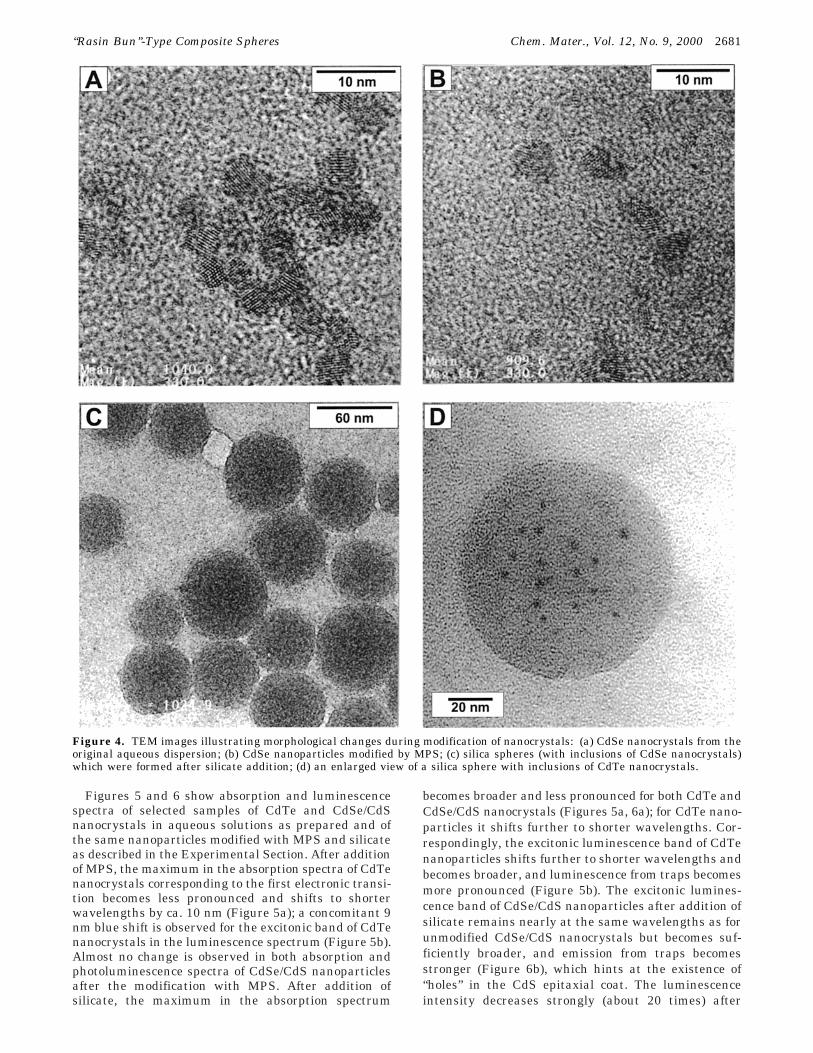
Morphological changes occurring during the modifica-tion of nanocrystals with MPS and silicate have beenfollowed by TEM (Figure 4). Unmodified nanocrystalstend to form agglomerates on the TEM grids when thesolvent is evaporated (Figure 4a). No formation of silicashells has been observed for nanocrystals whose surfaceis modified by MPS, although they appear to be moreisolated on TEM images (Figure 4b) than unmodifiedones, probably because of stronger steric and electro-static repulsion. After addition of silicate, SiO2 spheres40-80 nm in diameter are formed (Figure 4c) incolloidal solution, with semiconductor nanocrystals be-ing incorporated in silica as multiple cores (Figure 4d).
(45) Danek, M.; Jensen, K. F.; Murray, C. B.; Bawendi, M. G. Chem.Mater. 1996, 8, 173.
(46) Hines, M. A.; Guyot-Sionnest, P. J. Phys. Chem. 1996, 100,468.
(47) Dabbousi, B. O.; Rodriguez-Viejo, J.; Mikulec, F. V.; Heine, J.R.; Mattoussi, H.; Ober, R.; Jensen, K. F.; Bawendi, M. G. J. Phys.Chem. B 1997, 101, 9463.
(48) Peng, X.; Schlamp, M. C.; Kadavanich, A. V.; Alivisatos, A. P.J. Am. Chem. Soc. 1997, 119, 7019.
(49) Li, Y.; Xu, D.; Zhang, Q.; Chen, D.; Huang, F.; Xu, Y.; Guo, G.;Gu, Z. Chem. Mater. 1999, 11, 3433.
Figure 3. Absorption (a) and luminescence (b) spectra of“bare” CdSe nanoparticles (solid lines) and CdSe/CdS nano-particles (dashed lines). Both samples were heated in thesilicon oil bath at 70 °C for 24 h.
2680 Chem. Mater., Vol. 12, No. 9, 2000 Rogach et al.
Figures 5 and 6 show absorption and luminescencespectra of selected samples of CdTe and CdSe/CdSnanocrystals in aqueous solutions as prepared and ofthe same nanoparticles modified with MPS and silicateas described in the Experimental Section. After additionof MPS, the maximum in the absorption spectra of CdTenanocrystals corresponding to the first electronic transi-tion becomes less pronounced and shifts to shorterwavelengths by ca. 10 nm (Figure 5a); a concomitant 9nm blue shift is observed for the excitonic band of CdTenanocrystals in the luminescence spectrum (Figure 5b).Almost no change is observed in both absorption andphotoluminescence spectra of CdSe/CdS nanoparticlesafter the modification with MPS. After addition ofsilicate, the maximum in the absorption spectrum
becomes broader and less pronounced for both CdTe andCdSe/CdS nanocrystals (Figures 5a, 6a); for CdTe nano-particles it shifts further to shorter wavelengths. Cor-respondingly, the excitonic luminescence band of CdTenanoparticles shifts further to shorter wavelengths andbecomes broader, and luminescence from traps becomesmore pronounced (Figure 5b). The excitonic lumines-cence band of CdSe/CdS nanoparticles after addition ofsilicate remains nearly at the same wavelengths as forunmodified CdSe/CdS nanocrystals but becomes suf-ficiently broader, and emission from traps becomesstronger (Figure 6b), which hints at the existence of“holes” in the CdS epitaxial coat. The luminescenceintensity decreases strongly (about 20 times) after
Figure 4. TEM images illustrating morphological changes during modification of nanocrystals: (a) CdSe nanocrystals from theoriginal aqueous dispersion; (b) CdSe nanoparticles modified by MPS; (c) silica spheres (with inclusions of CdSe nanocrystals)which were formed after silicate addition; (d) an enlarged view of a silica sphere with inclusions of CdTe nanocrystals.
“Rasin Bun”-Type Composite Spheres Chem. Mater., Vol. 12, No. 9, 2000 2681

silicate addition to both CdTe and CdSe/CdS nanopar-ticles, in comparison with unmodified nanocrystals.
Changes in absorption and luminescence spectraobserved for the citrate-stabilized CdSe nanocrystalsdue to MPS and silicate modification repeat those forCdSe/CdS nanoparticles. Luminescence of MPS- andsilicate-modified bare CdSe nanoparticles, being weakenough for unmodified CdSe nanocrystals, almost com-pletely disappears, while the CdSe/CdS core-shells stillshow noticeable luminescence.
The further growth of silica spheres from 40 to 80 nmin diameter (Figure 4c) to 200-400 nm, for which thephotonic band gap effects can be observed in the visibleregion, can be performed by the Stober technique42 usingeither MPS-modified semiconductor nanocrystals or“raisin bun”-type composite particles as seeds. Thisprocess yields silica globules in the range of 100-700nm, which is quite convenient for further studies.27
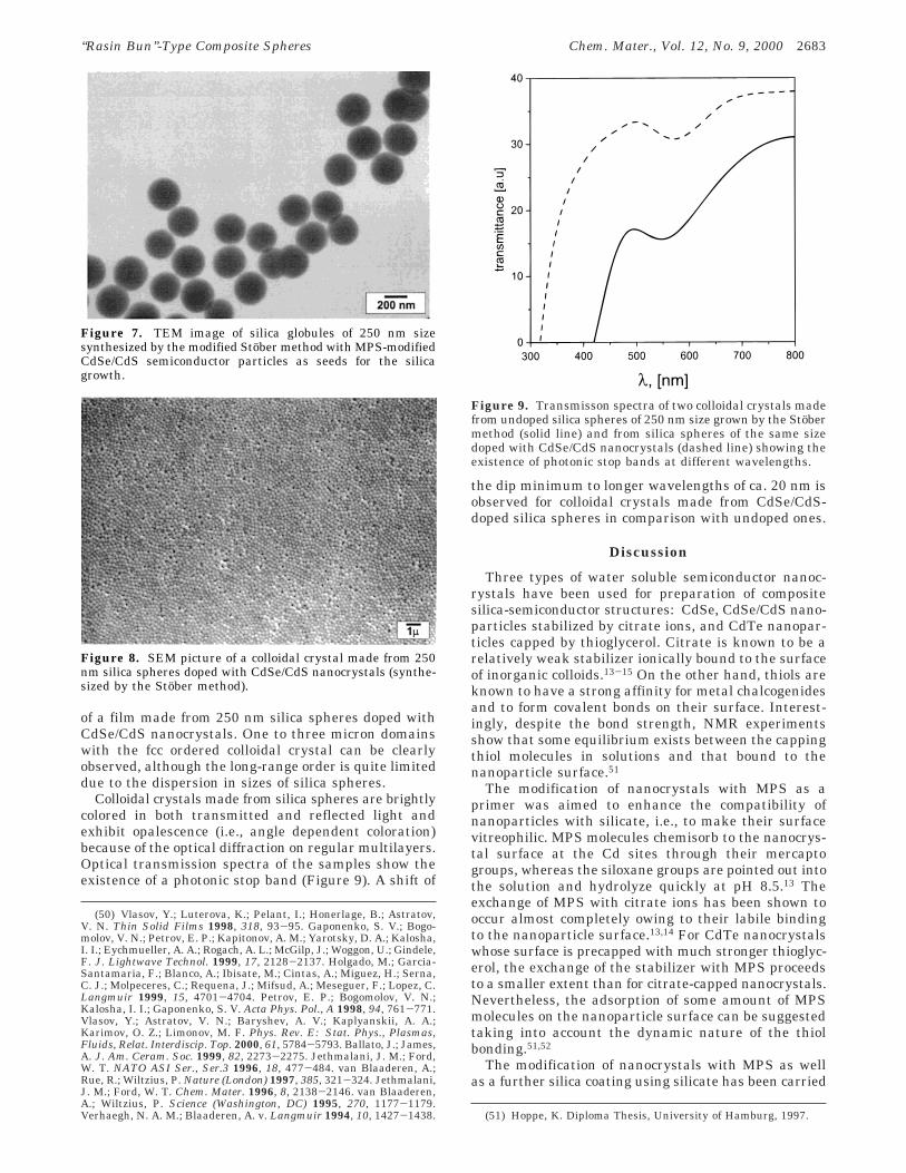
Figure 7 shows a TEM image of silica globules of 250
nm size synthesized by the modified Stober method withMPS-modified CdSe/CdS semiconductor particles asseeds for the silica growth. Composite particles formedhave yellowish color because of the CdSe/CdS doping.Unfortunately, large diameter of the colloid made itimpossible to view semiconductor nanocrystals incor-porated in large silica spheres with a transmissionelectron microscope. “Raisin bun”-type composite par-ticles can be used as seeds in the Stober synthesis aswell, giving structures with a thick silica shell and a40-80 nm core where semiconductor nanocrystals areto be confined.
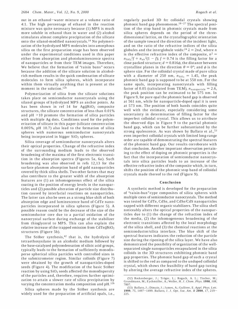
Colloidal Crystals Made from Doped SilicaSpheres. When allowed to sediment, charge-stabilizedsubmicrometer-size silica spheres can organize them-selves into a 3D regular lattice.28-39,50 Similarly, evapo-ration of the solvent from the nanoparticle-doped SiO2leads to colloidal crystals. Figure 8 shows a SEM picture
Figure 5. Absorption (a) and luminescence (b) spectra ofunmodified CdTe nanocrystals (solid lines), CdTe nanocrystalsmodified with MPS (dashed lines) and composite CdTe@SiO2
spheres formed after silicate addition (dotted lines).
Figure 6. Absorption (a) and luminescence (b) spectra ofunmodified CdSe/CdS nanocrystals (solid lines) and compositeCdSe/CdS@SiO2 spheres formed after silicate addition (dottedlines). Absorption and photoluminescence spectra of CdSe/CdSnanoparticles modified with MPS are almost the same as forunmodified CdSe/CdS nanocrystals and are not shown here.
2682 Chem. Mater., Vol. 12, No. 9, 2000 Rogach et al.
of a film made from 250 nm silica spheres doped withCdSe/CdS nanocrystals. One to three micron domainswith the fcc ordered colloidal crystal can be clearlyobserved, although the long-range order is quite limiteddue to the dispersion in sizes of silica spheres.
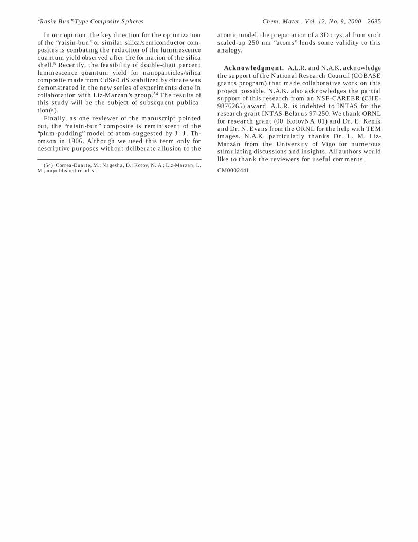
Colloidal crystals made from silica spheres are brightlycolored in both transmitted and reflected light andexhibit opalescence (i.e., angle dependent coloration)because of the optical diffraction on regular multilayers.Optical transmission spectra of the samples show theexistence of a photonic stop band (Figure 9). A shift of
the dip minimum to longer wavelengths of ca. 20 nm isobserved for colloidal crystals made from CdSe/CdS-doped silica spheres in comparison with undoped ones.
Discussion
Three types of water soluble semiconductor nanoc-rystals have been used for preparation of compositesilica-semiconductor structures: CdSe, CdSe/CdS nano-particles stabilized by citrate ions, and CdTe nanopar-ticles capped by thioglycerol. Citrate is known to be arelatively weak stabilizer ionically bound to the surfaceof inorganic colloids.13-15 On the other hand, thiols areknown to have a strong affinity for metal chalcogenidesand to form covalent bonds on their surface. Interest-ingly, despite the bond strength, NMR experimentsshow that some equilibrium exists between the cappingthiol molecules in solutions and that bound to thenanoparticle surface.51
The modification of nanocrystals with MPS as aprimer was aimed to enhance the compatibility ofnanoparticles with silicate, i.e., to make their surfacevitreophilic. MPS molecules chemisorb to the nanocrys-tal surface at the Cd sites through their mercaptogroups, whereas the siloxane groups are pointed out intothe solution and hydrolyze quickly at pH 8.5.13 Theexchange of MPS with citrate ions has been shown tooccur almost completely owing to their labile bindingto the nanoparticle surface.13,14 For CdTe nanocrystalswhose surface is precapped with much stronger thioglyc-erol, the exchange of the stabilizer with MPS proceedsto a smaller extent than for citrate-capped nanocrystals.Nevertheless, the adsorption of some amount of MPSmolecules on the nanoparticle surface can be suggestedtaking into account the dynamic nature of the thiolbonding.51,52
The modification of nanocrystals with MPS as wellas a further silica coating using silicate has been carried
(50) Vlasov, Y.; Luterova, K.; Pelant, I.; Honerlage, B.; Astratov,V. N. Thin Solid Films 1998, 318, 93-95. Gaponenko, S. V.; Bogo-molov, V. N.; Petrov, E. P.; Kapitonov, A. M.; Yarotsky, D. A.; Kalosha,I. I.; Eychmueller, A. A.; Rogach, A. L.; McGilp, J.; Woggon, U.; Gindele,F. J. Lightwave Technol. 1999, 17, 2128-2137. Holgado, M.; Garcia-Santamaria, F.; Blanco, A.; Ibisate, M.; Cintas, A.; Miguez, H.; Serna,C. J.; Molpeceres, C.; Requena, J.; Mifsud, A.; Meseguer, F.; Lopez, C.Langmuir 1999, 15, 4701-4704. Petrov, E. P.; Bogomolov, V. N.;Kalosha, I. I.; Gaponenko, S. V. Acta Phys. Pol., A 1998, 94, 761-771.Vlasov, Y.; Astratov, V. N.; Baryshev, A. V.; Kaplyanskii, A. A.;Karimov, O. Z.; Limonov, M. F. Phys. Rev. E: Stat. Phys., Plasmas,Fluids, Relat. Interdiscip. Top. 2000, 61, 5784-5793. Ballato, J.; James,A. J. Am. Ceram. Soc. 1999, 82, 2273-2275. Jethmalani, J. M.; Ford,W. T. NATO ASI Ser., Ser.3 1996, 18, 477-484. van Blaaderen, A.;Rue, R.; Wiltzius, P. Nature (London) 1997, 385, 321-324. Jethmalani,J. M.; Ford, W. T. Chem. Mater. 1996, 8, 2138-2146. van Blaaderen,A.; Wiltzius, P. Science (Washington, DC) 1995, 270, 1177-1179.Verhaegh, N. A. M.; Blaaderen, A. v. Langmuir 1994, 10, 1427-1438. (51) Hoppe, K. Diploma Thesis, University of Hamburg, 1997.
Figure 7. TEM image of silica globules of 250 nm sizesynthesized by the modified Stober method with MPS-modifiedCdSe/CdS semiconductor particles as seeds for the silicagrowth.
Figure 8. SEM picture of a colloidal crystal made from 250nm silica spheres doped with CdSe/CdS nanocrystals (synthe-sized by the Stober method).
Figure 9. Transmisson spectra of two colloidal crystals madefrom undoped silica spheres of 250 nm size grown by the Stobermethod (solid line) and from silica spheres of the same sizedoped with CdSe/CdS nanocrystals (dashed line) showing theexistence of photonic stop bands at different wavelengths.
“Rasin Bun”-Type Composite Spheres Chem. Mater., Vol. 12, No. 9, 2000 2683
out in an ethanol-water mixture at a volume ratio of4:1. The high percentage of ethanol in the reactionmixture was quite necessary because (1) MPS is muchmore soluble in ethanol than in water and (2) alcoholstimulates almost complete precipitation of the silicateonto the silanol-modified nanocrystals.14 No polymeri-zation of the hydrolyzed MPS molecules into amorphoussilica on the first preparation stage has been observedunder the experimental conditions used in this papereither from absorption and photoluminescence spectraof nanoparticles or from their TEM images. Therefore,We believe that the formation of “raisin buns” occursbecause the addition of the silicate solution in alcohol-rich medium results in the quick condensation of silicatemolecules to form silica spheres, which incorporatewithin them virtually anything that is present at themoment in the solution.12b
Polymerization of silica from the silicate solutionstakes place on semiconductor nanocrystals using thesilanol groups of hydrolyzed MPS as anchor points. Ashas been shown in ref 14 for Ag@SiO2 compositestructures, the silicate concentration of less than 0.01%and pH >10 promote the formation of silica particleswith multiple Ag dots. Conditions used for the polym-erization of silicate in this paper (silicate concentration0.005%, pH 10.7) also lead to the formation of silicaspheres with numerous semiconductor nanocrystalsbeing incorporated in bigger SiO2 spheres.
Silica coverage of semiconductor nanocrystals alterstheir optical properties. Change of the refractive indexof the surrounding medium leads to the observedbroadening of the maxima of the first electronic transi-tion in the absorption spectra (Figures 5a, 6a). Suchbroadening was also observed in refs 12,13 for thesurface plasmon absorption band of gold nanoparticlescovered by thick silica shells. Two other factors that mayalso contribute to the greater width of the absorptionfeatures are (1) an inhomogeneous effect of the silicacoating in the position of energy levels in the nanopar-ticles and (2) possible alteration of particle size distribu-tion caused by interfacial reactions on nanoparticles.The latter can also be seen as a strong blue shift of bothabsorption edge and luminescence band of CdTe nano-particles incorporated in silica spheres (Figure 5). Apossible reason could be the decrease of the size of thesemiconductor core due to a partial oxidation of thenanocrystal surface during exchange of the stabilizerfrom thioglycerol to MPS. This can also explain therelative increase of the trapped emission from CdTe@SiO2structures (Figure 5b).
The Stober synthesis,42 that is, the hydrolysis oftetraethoxysilane in an alcoholic medium followed bythe base-catalyzed polycondensation of silicic acid groups,typically leads to the formation of sufficiently monodis-perse spherical silica particles with controlled sizes inthe submicrometer region. Similar colloids (Figure 7)were obtained by the growth of nanoparticles-dopedseeds (Figure 4). The modification of the basic Stoberreaction by using SiO2 seeds affected the monodispersityof the particles and, therefore, requires further optimi-zation to attain a slower rate of silica precipitation byvarying the concentration media composition and pH.12b
Silica spheres made by the Stober synthesis arewidely used for the preparation of artificial opals, i.e.,
regularly packed 3D fcc colloidal crystals showingphotonic band gap phenomenon.18-27 The spectral posi-tion of the stop band in photonic crystals made fromsilica spheres depends on the period of the three-dimensional lattice, on the crystallographic orientationof the sample toward the direction of the incident light,and on the ratio of the refractive indices of the silicaglobules and the interglobule voids:24 λ ) 2nd, where nis the effective refractive index of the composite, n2 )nSiO2
2f + nair2(1 - f); f ) 0.74 is the filling factor for a
close packed structure; d ) 0.816φ, the distance betweencrystalline planes in the direction θ ) 0°; and φ is thesphere size. For the colloidal crystal made of pure silicawith a diameter of 250 nm, nSiO2 ) 1.45, the peakphotonic band gap is supposed to be at 550 nm. For thesame opals, incorporating nanocrystals with fillingfactor of 0.05 (calculated from TEM), nnanoparticle ) 2.6,the peak position can be estimated to be 575 nm. InFigure 9, for pure opal the photonic band gap is observedat 561 nm, while for nanoparticle-doped opal it is seenat 573 nm. The position of both bands coincides quitewell with the estimate, especially considering someuncertainty in determination of filling factor for theimperfect colloidal crystal. This allows us to attributethe observed dips in Figure 9 to the partial photonicband gap, which can be further substantiated by thestrong opalescence. As was shown by Ballato et al.,53
even imperfect colloidal crystals with limited long-rangeorder are capable of demonstrating the spectral featuresof the photonic band gap. Our results corroborate withthat conclusion. Another important observation pertain-ing to the effect of doping on photonic properties is thefact that the incorporation of semiconductor nanocrys-tals into silica particles leads to an increase of theeffective refractive index of the composite which, in turn,shifts the position of the photonic stop band of colloidalcrystals made thereof to the red (Figure 9).
Conclusion
A synthetic method is developed for the preparationof “raisin-bun”-type composites of silica spheres withmultiple cores of semiconductor nanocrystals. The methodwas tested for CdTe, CdSe, and CdSe/CdS nanoparticlescapped with different organic stabilizers. The silica shellnoticeably alters the optical properties of the nanopar-ticles due to (1) the change of the refraction index ofthe media, (2) the inhomogeneous broadening of theelectronic transitions affected by the local morphologyof the silica shell, and (3) the chemical reactions at thesemiconductor/silica interface. The blue shift of thespectral features indicates the reduction of the particlesize during the ripening of the silica layer. We have alsodemonstrated the possibility of organization of the well-separated single nanoparticles encapsulated in the silicacolloids in the 3D structures exhibiting photonic bandgap properties. The photonic band gap of such a crystalis shifted to the red as compared to the undoped colloidalcrystal, which shows the feasibility of band gap tuningby altering the average refractive index of the spheres.
(52) Rockenberger, J.; Troger, L.; Rogach, A. L.; Tischer, M.;Grundmann, M.; Eychmuller, A.; Weller, H. J. Chem. Phys. 1998, 108,7807.
(53) Ballato, J.; Dimaio, J.; James, A.; Gulliver, E. Appl. Phys. Lett.1999, 75, 1497-1499. Ballato, J. J. Opt. Soc. Am. B 2000, 17, 219-225.
2684 Chem. Mater., Vol. 12, No. 9, 2000 Rogach et al.
In our opinion, the key direction for the optimizationof the “raisin-bun” or similar silica/semiconductor com-posites is combating the reduction of the luminescencequantum yield observed after the formation of the silicashell.5 Recently, the feasibility of double-digit percentluminescence quantum yield for nanoparticles/silicacomposite made from CdSe/CdS stabilized by citrate wasdemonstrated in the new series of experiments done incollaboration with Liz-Marzan’s group.54 The results ofthis study will be the subject of subsequent publica-tion(s).
Finally, as one reviewer of the manuscript pointedout, the “raisin-bun” composite is reminiscent of the“plum-pudding” model of atom suggested by J. J. Th-omson in 1906. Although we used this term only fordescriptive purposes without deliberate allusion to the
atomic model, the preparation of a 3D crystal from suchscaled-up 250 nm “atoms” lends some validity to thisanalogy.
Acknowledgment. A.L.R. and N.A.K. acknowledgethe support of the National Research Council (COBASEgrants program) that made collaborative work on thisproject possible. N.A.K. also acknowledges the partialsupport of this research from an NSF-CAREER (CHE-9876265) award. A.L.R. is indebted to INTAS for theresearch grant INTAS-Belarus 97-250. We thank ORNLfor research grant (00 KotovNA 01) and Dr. E. Kenikand Dr. N. Evans from the ORNL for the help with TEMimages. N.A.K. particularly thanks Dr. L. M. Liz-Marzan from the University of Vigo for numerousstimulating discussions and insights. All authors wouldlike to thank the reviewers for useful comments.
CM000244I(54) Correa-Duarte, M.; Nagesha, D.; Kotov, N. A.; Liz-Marzan, L.
M.; unpublished results.
“Rasin Bun”-Type Composite Spheres Chem. Mater., Vol. 12, No. 9, 2000 2685
Related Documents