123 SPRINGER BRIEFS IN ELECTRICAL AND COMPUTER ENGINEERING Saleh Faruque Radio Frequency Source Coding Made Easy

Welcome message from author
This document is posted to help you gain knowledge. Please leave a comment to let me know what you think about it! Share it to your friends and learn new things together.
Transcript

123
S P R I N G E R B R I E F S I N E L E C T R I C A L A N D CO M P U T E R E N G I N E E R I N G
Saleh Faruque
Radio Frequency Source Coding Made Easy
SpringerBriefs in Electrical and ComputerEngineering
More information about this series at http://www.springer.com/series/10059

Saleh Faruque
Radio Frequency SourceCoding Made Easy

Saleh FaruqueDepartment of Electrical EngineeringUniversity of North DakotaGrand Forks, ND, USA
ISSN 2191-8112 ISSN 2191-8120 (electronic)SpringerBriefs in Electrical and Computer EngineeringISBN 978-3-319-15608-8 ISBN 978-3-319-15609-5 (eBook)DOI 10.1007/978-3-319-15609-5
Library of Congress Control Number: 2015938589
Springer Cham Heidelberg New York Dordrecht London© Springer International Publishing Switzerland 2015This work is subject to copyright. All rights are reserved by the Publisher, whether the whole or part ofthe material is concerned, specifically the rights of translation, reprinting, reuse of illustrations,recitation, broadcasting, reproduction on microfilms or in any other physical way, and transmissionor information storage and retrieval, electronic adaptation, computer software, or by similar ordissimilar methodology now known or hereafter developed.The use of general descriptive names, registered names, trademarks, service marks, etc. in thispublication does not imply, even in the absence of a specific statement, that such names are exemptfrom the relevant protective laws and regulations and therefore free for general use.The publisher, the authors and the editors are safe to assume that the advice and information in thisbook are believed to be true and accurate at the date of publication. Neither the publisher nor theauthors or the editors give a warranty, express or implied, with respect to the material containedherein or for any errors or omissions that may have been made.
Printed on acid-free paper
Springer International Publishing AG Switzerland is part of Springer Science+Business Media(www.springer.com)

Preface
In communications engineering, source coding is the first step of processing input
signals before transmission. The main focus of source coding is to:
• Identify
• Quantify
• Band limit
• Convert analog signals into digital format
The next step after source coding is to use:
• Forward error control coding (FECC) to detect and correct errors
• A suitable modulation scheme to transmit the modulated signal through an
antenna.
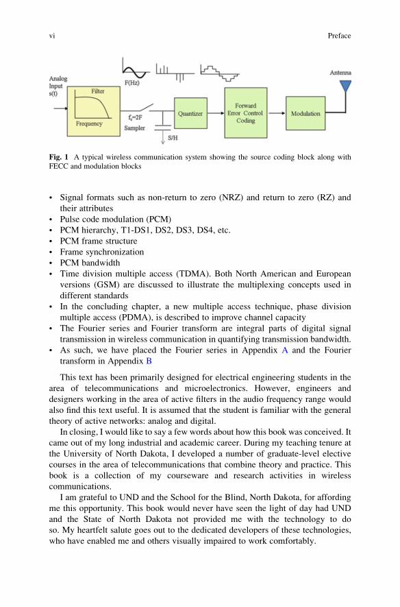
Figure 1 illustrates the process. At the transmit side, the source coding is referred
to as encoder. At the receive side, it is referred to as source decoder. It is a reverse
process, which is not shown in the figure.
In this book, source coding is discussed in detail. Later books in this series will
cover FECC and modulation.
Presented in this book are the salient concepts, underlying principles, and
practical applications of source coding. In particular, this book will address the
following topics as related to source coding:
• Identification and characterization of input signals such as analog signal, digital
signal, and noise
• Signal-to-noise ratio and its effects in communication channels
• Shannon’s capacity theorem and its attributes
• Measurement and quantification of signals
• Band limit filters based on active analog and MOS switched capacitor
technology
• Nyquist sampling theorem
• Shannon’s capacity theorem
• Quantization: linear and nonlinear
v
• Signal formats such as non-return to zero (NRZ) and return to zero (RZ) and
their attributes
• Pulse code modulation (PCM)
• PCM hierarchy, T1-DS1, DS2, DS3, DS4, etc.
• PCM frame structure
• Frame synchronization
• PCM bandwidth
• Time division multiple access (TDMA). Both North American and European
versions (GSM) are discussed to illustrate the multiplexing concepts used in
different standards
• In the concluding chapter, a new multiple access technique, phase division
multiple access (PDMA), is described to improve channel capacity
• The Fourier series and Fourier transform are integral parts of digital signal
transmission in wireless communication in quantifying transmission bandwidth.
• As such, we have placed the Fourier series in Appendix A and the Fourier
transform in Appendix B
This text has been primarily designed for electrical engineering students in the
area of telecommunications and microelectronics. However, engineers and
designers working in the area of active filters in the audio frequency range would
also find this text useful. It is assumed that the student is familiar with the general
theory of active networks: analog and digital.
In closing, I would like to say a few words about how this book was conceived. It
came out of my long industrial and academic career. During my teaching tenure at
the University of North Dakota, I developed a number of graduate-level elective
courses in the area of telecommunications that combine theory and practice. This
book is a collection of my courseware and research activities in wireless
communications.
I am grateful to UND and the School for the Blind, North Dakota, for affording
me this opportunity. This book would never have seen the light of day had UND
and the State of North Dakota not provided me with the technology to do
so. My heartfelt salute goes out to the dedicated developers of these technologies,
who have enabled me and others visually impaired to work comfortably.
Fig. 1 A typical wireless communication system showing the source coding block along with
FECC and modulation blocks
vi Preface

Finally, I would like to thank my beloved wife, Yasmin, an English Literature
buff and a writer herself, for being by my side throughout the writing of this book
and for patiently proofreading it. My darling son, Shams, an electrical engineer
himself, provided technical support when I needed it. For this, he deserves my
heartfelt thanks.
In spite of all this support, there may still be some errors in this book. I hope
that my readers forgive me for them. I shall be amply rewarded if they still find
this book useful.
Grand Forks, ND, USA Saleh Faruque
Preface vii

Contents
1 Introduction to Source Coding . . . . . . . . . . . . . . . . . . . . . . . . . . . . . 1
1.1 Source Coding Defined . . . . . . . . . . . . . . . . . . . . . . . . . . . . . . . 1
1.2 Identification and Characterization of Input Signals . . . . . . . . . . 2
1.2.1 Periodic Analog Signals . . . . . . . . . . . . . . . . . . . . . . . . 3
1.2.2 Non-periodic Analog Signals . . . . . . . . . . . . . . . . . . . . 4
1.2.3 Periodic Digital Signals . . . . . . . . . . . . . . . . . . . . . . . . 5
1.2.4 A Non-periodic Digital Signals . . . . . . . . . . . . . . . . . . . 8
1.2.5 Clock and Data . . . . . . . . . . . . . . . . . . . . . . . . . . . . . . 10
1.3 Noise . . . . . . . . . . . . . . . . . . . . . . . . . . . . . . . . . . . . . . . . . . . . 12
1.3.1 Background . . . . . . . . . . . . . . . . . . . . . . . . . . . . . . . . . 12
1.3.2 Thermal Noise . . . . . . . . . . . . . . . . . . . . . . . . . . . . . . . 13
1.3.3 Shot Noise . . . . . . . . . . . . . . . . . . . . . . . . . . . . . . . . . . 13
1.4 Interference . . . . . . . . . . . . . . . . . . . . . . . . . . . . . . . . . . . . . . . 14
1.4.1 Co-Channel Interference . . . . . . . . . . . . . . . . . . . . . . . 14
1.4.2 C/I Due to Multiple Interferers . . . . . . . . . . . . . . . . . . . 15
1.4.3 The Effect of Noise in Communication
Channels and Shannon’s Capacity Theorem . . . . . . . . . 17
1.5 Measurement and Quantification of Signals . . . . . . . . . . . . . . . . 18
1.5.1 Decimal System . . . . . . . . . . . . . . . . . . . . . . . . . . . . . . 19
1.5.2 Binary System . . . . . . . . . . . . . . . . . . . . . . . . . . . . . . . 19
1.6 Conclusions . . . . . . . . . . . . . . . . . . . . . . . . . . . . . . . . . . . . . . . 20
References . . . . . . . . . . . . . . . . . . . . . . . . . . . . . . . . . . . . . . . . . . . . . 20
2 Baseband Filters: Active RC Filters . . . . . . . . . . . . . . . . . . . . . . . . . 21
2.1 Introduction . . . . . . . . . . . . . . . . . . . . . . . . . . . . . . . . . . . . . . . 21
2.2 Voltage to Current Source . . . . . . . . . . . . . . . . . . . . . . . . . . . . . 22
2.3 Voltage to Current Transducer (Transconductance) . . . . . . . . . . 22
2.4 Amplifiers . . . . . . . . . . . . . . . . . . . . . . . . . . . . . . . . . . . . . . . . 23
2.4.1 Differential Amplifier . . . . . . . . . . . . . . . . . . . . . . . . . 23
2.4.2 Inverting Amplifier . . . . . . . . . . . . . . . . . . . . . . . . . . . 24
2.4.3 Non-inverting Amplifier . . . . . . . . . . . . . . . . . . . . . . . . 25
ix
2.5 Integrators Based on Transconductances . . . . . . . . . . . . . . . . . . 26
2.6 Differential Integrators . . . . . . . . . . . . . . . . . . . . . . . . . . . . . . . 26
2.7 Simulation of Grounded Inductor . . . . . . . . . . . . . . . . . . . . . . . 29
2.8 Simulation of Floating Inductor . . . . . . . . . . . . . . . . . . . . . . . . . 30
2.9 Second Order Filters: The Biquad . . . . . . . . . . . . . . . . . . . . . . . 32
2.9.1 Lowpass Filter . . . . . . . . . . . . . . . . . . . . . . . . . . . . . . . 32
2.9.2 High Pass Filter . . . . . . . . . . . . . . . . . . . . . . . . . . . . . . 32
2.9.3 Bandpass Filter . . . . . . . . . . . . . . . . . . . . . . . . . . . . . . 33
2.9.4 Band Reject Filters . . . . . . . . . . . . . . . . . . . . . . . . . . . 33
2.10 Active Filters Based on Simulated Inductors . . . . . . . . . . . . . . . 36
2.10.1 LC Prototype Filter . . . . . . . . . . . . . . . . . . . . . . . . . . . 36
2.10.2 Transconductance Model of the Prototype Filter . . . . . . 37
2.10.3 RC Active Equivalent of the LC Prototype Filter . . . . . . 39
2.11 Higher Order Filters . . . . . . . . . . . . . . . . . . . . . . . . . . . . . . . . . 42
2.11.1 Third Order Lowpass Ladder Filter . . . . . . . . . . . . . . . . 42
2.11.2 Fifth Order Lowpass Ladder Filter . . . . . . . . . . . . . . . . 44
2.12 Conclusions . . . . . . . . . . . . . . . . . . . . . . . . . . . . . . . . . . . . . . . 46
References . . . . . . . . . . . . . . . . . . . . . . . . . . . . . . . . . . . . . . . . . . . . . 46
3 Switched Capacitor Building Blocks and Filters . . . . . . . . . . . . . . . . 47
3.1 Switched Capacitor Resistor . . . . . . . . . . . . . . . . . . . . . . . . . . . 47
3.2 Switched-Capacitor Integrators and Transconductances . . . . . . . 49
3.3 Differential Integrator . . . . . . . . . . . . . . . . . . . . . . . . . . . . . . . . 50
3.4 Z-Domain Analysis . . . . . . . . . . . . . . . . . . . . . . . . . . . . . . . . . 51
3.4.1 Switched Capacitor (Sc) Resistor . . . . . . . . . . . . . . . . . 51
3.4.2 Switched Capacitor (sC) Integrator . . . . . . . . . . . . . . . . 52
3.4.3 Frequency Response of SC-Integrator . . . . . . . . . . . . . . 54
3.5 Switched-Capacitor Biquad Filters . . . . . . . . . . . . . . . . . . . . . . . 55
3.5.1 Lowpass Filter . . . . . . . . . . . . . . . . . . . . . . . . . . . . . . . 55
3.5.2 Bandpass Filter . . . . . . . . . . . . . . . . . . . . . . . . . . . . . . 56
3.5.3 Switched Capacitor Biquad . . . . . . . . . . . . . . . . . . . . . 56
3.6 Switched-Capacitor Filters Based on Simulated Inductors . . . . . . 59
3.6.1 SC Realization of Second Order LC Filters . . . . . . . . . . 60
3.6.2 SC Realization of Third Order LC Ladder Filters . . . . . 61
3.7 Conclusions . . . . . . . . . . . . . . . . . . . . . . . . . . . . . . . . . . . . . . . 64
References . . . . . . . . . . . . . . . . . . . . . . . . . . . . . . . . . . . . . . . . . . . . . 64
4 Pulse Code Modulation (PCM) . . . . . . . . . . . . . . . . . . . . . . . . . . . . . 65
4.1 Introduction to PCM . . . . . . . . . . . . . . . . . . . . . . . . . . . . . . . . . 65
4.2 Input Band-Limit Filter . . . . . . . . . . . . . . . . . . . . . . . . . . . . . . . 66
4.3 Sampling . . . . . . . . . . . . . . . . . . . . . . . . . . . . . . . . . . . . . . . . . 67
4.4 Aliasing . . . . . . . . . . . . . . . . . . . . . . . . . . . . . . . . . . . . . . . . . . 68
4.4.1 Spectrum of Analog Signals Before Sampling . . . . . . . . 68
4.4.2 Spectral Response Due to Nyquist Sampling . . . . . . . . . 69
4.4.3 Spectral Response Due to Oversampling (fs> 2 fm) . . . . 69
4.4.4 Spectral Response Due to Under Sampling (Aliasing) . . . 69
x Contents
4.5 Quantization . . . . . . . . . . . . . . . . . . . . . . . . . . . . . . . . . . . . . . . 72
4.5.1 Linear Quantization . . . . . . . . . . . . . . . . . . . . . . . . . . . 72
4.5.2 Drawback of Linear Quantization . . . . . . . . . . . . . . . . . 73
4.6 Non-linear Quantization . . . . . . . . . . . . . . . . . . . . . . . . . . . . . . 74
4.7 Companding . . . . . . . . . . . . . . . . . . . . . . . . . . . . . . . . . . . . . . . 74
4.8 Digital to Analog Converter . . . . . . . . . . . . . . . . . . . . . . . . . . . 76
4.9 Analog to Digital Converter . . . . . . . . . . . . . . . . . . . . . . . . . . . 78
4.9.1 Function of the Comparator . . . . . . . . . . . . . . . . . . . . . 79
4.9.2 Function of the Up/Down Counter . . . . . . . . . . . . . . . . 79
4.9.3 Function of the D/A Converter . . . . . . . . . . . . . . . . . . . 80
4.9.4 Overall Function of the A/D-D/A Converter . . . . . . . . . 80
4.10 Resolution . . . . . . . . . . . . . . . . . . . . . . . . . . . . . . . . . . . . . . . . 83
4.11 Binary Line Coding and Power Spectrum . . . . . . . . . . . . . . . . . 84
4.11.1 Popular Binary Signaling Formats . . . . . . . . . . . . . . . . 85
4.12 Bit Rate . . . . . . . . . . . . . . . . . . . . . . . . . . . . . . . . . . . . . . . . . . 87
4.13 Bandwidth . . . . . . . . . . . . . . . . . . . . . . . . . . . . . . . . . . . . . . . . 88
4.14 Conclusions . . . . . . . . . . . . . . . . . . . . . . . . . . . . . . . . . . . . . . . 89
References . . . . . . . . . . . . . . . . . . . . . . . . . . . . . . . . . . . . . . . . . . . . . 89
5 Time Division Multiplexing (TDM) . . . . . . . . . . . . . . . . . . . . . . . . . . 91
5.1 Introduction . . . . . . . . . . . . . . . . . . . . . . . . . . . . . . . . . . . . . . . 91
5.2 North American TDM in Digital Telephony . . . . . . . . . . . . . . . . 94
5.2.1 The Basic TDM Structure . . . . . . . . . . . . . . . . . . . . . . 94
5.2.2 Distributed Frame Structure . . . . . . . . . . . . . . . . . . . . . 95
5.2.3 Bunched Frame Structure . . . . . . . . . . . . . . . . . . . . . . . 96
5.3 European TDM in Digital Telephony . . . . . . . . . . . . . . . . . . . . . 97
5.4 Frame Synchronization . . . . . . . . . . . . . . . . . . . . . . . . . . . . . . . 98
5.4.1 Synchronization Process . . . . . . . . . . . . . . . . . . . . . . . . 98
5.4.2 Estimation of Frame Error Rate . . . . . . . . . . . . . . . . . . 98
5.5 North American TDM Hierarchy . . . . . . . . . . . . . . . . . . . . . . . . 101
5.6 Time Division Multiple Access (TDMA) . . . . . . . . . . . . . . . . . . 102
5.6.1 The North American TDMA . . . . . . . . . . . . . . . . . . . . 102
5.6.2 North American TDMA Scheme . . . . . . . . . . . . . . . . . 103
5.6.3 TDMA Transmission Format . . . . . . . . . . . . . . . . . . . . 104
5.6.4 TDMA Time Slots and Data Field Structure . . . . . . . . . 105
5.7 Global System for Mobile Communication (GSM) . . . . . . . . . . . 108
5.7.1 GSM TDMA Scheme . . . . . . . . . . . . . . . . . . . . . . . . . . 108
5.7.2 GSM TDMA Frame (4.615 ms) . . . . . . . . . . . . . . . . . . 108
5.7.3 GSM TDMA Frame Hierarchy . . . . . . . . . . . . . . . . . . . 109
5.8 TDMA Performance . . . . . . . . . . . . . . . . . . . . . . . . . . . . . . . . . 111
5.8.1 Uncoded and Coded BER . . . . . . . . . . . . . . . . . . . . . . . 111
5.8.2 BER as a Function of Mobile Speed . . . . . . . . . . . . . . . 112
5.9 Conclusions . . . . . . . . . . . . . . . . . . . . . . . . . . . . . . . . . . . . . . . 115
References . . . . . . . . . . . . . . . . . . . . . . . . . . . . . . . . . . . . . . . . . . . . . 118
Contents xi

6 Phase Division Multiple Access (PDMA) . . . . . . . . . . . . . . . . . . . . . 119
6.1 Introduction . . . . . . . . . . . . . . . . . . . . . . . . . . . . . . . . . . . . . . . 119
6.2 Properties of Orthogonal Codes . . . . . . . . . . . . . . . . . . . . . . . . . 121
6.2.1 Orthogonal and Biorthogonal Codes . . . . . . . . . . . . . . . 121
6.2.2 Cross-Correlation Properties of Orthogonal Codes . . . . . 122
6.2.3 Error control Properties of Orthogonal Codes . . . . . . . . 123
6.3 Multiple User PDMA . . . . . . . . . . . . . . . . . . . . . . . . . . . . . . . . 124
6.3.1 Construction of PDMA2 . . . . . . . . . . . . . . . . . . . . . . . . 124
6.3.2 Construction of PDMA4 . . . . . . . . . . . . . . . . . . . . . . . . 126
6.3.3 Hybrid TDMA-PDMA Structure . . . . . . . . . . . . . . . . . . 127
6.4 Ber Performance Analysis . . . . . . . . . . . . . . . . . . . . . . . . . . . . . 128
6.5 Conclusions . . . . . . . . . . . . . . . . . . . . . . . . . . . . . . . . . . . . . . . 131
References . . . . . . . . . . . . . . . . . . . . . . . . . . . . . . . . . . . . . . . . . . . . . 132
Appendix A . . . . . . . . . . . . . . . . . . . . . . . . . . . . . . . . . . . . . . . . . . . . . . 133
Appendix B . . . . . . . . . . . . . . . . . . . . . . . . . . . . . . . . . . . . . . . . . . . . . . 141
xii Contents
Chapter 1
Introduction to Source Coding
Topics
• Introduction to Source Coding
• Signals and Spectra
• Noise and Interference
• Effects of Noise on Communication Circuits and Shannon’s Capacity Theorem
• Measurement and Quantification of signals in Noise, Interference and Fading
1.1 Source Coding Defined
In communications engineering, source coding is the first step of processing input
signals, (analog and/or digital). It identifies, quantifies, band limits, and converts
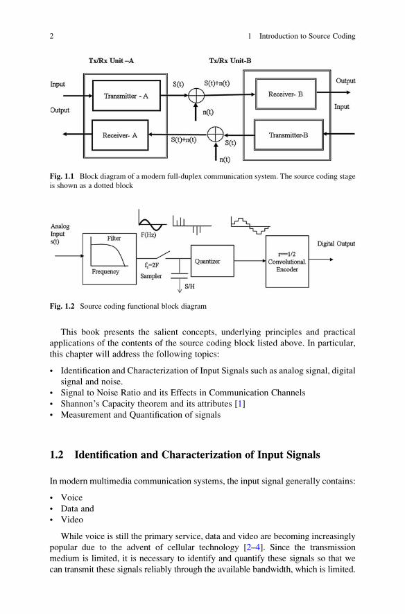
the analog signals into Digital formats. Figure 1.1 shows the conceptual block
diagram of a modern wireless communication system, where the source coding
block is shown in the inset of the dotted block. At the transmit side, the source
coding is referred to as encoder and at the receive side, it is referred to as source
decoder.
Figure 1.2 shows the basic functional block diagram of a typical source coding.
It Involves:
• Identification and Characterization of input signals
• Band limiting the input signal by means of filters
• Sampling and Quantization the input signal
• A/D-D/A Conversion
• Estimation of Bandwidth
© Springer International Publishing Switzerland 2015
S. Faruque, Radio Frequency Source Coding Made Easy, SpringerBriefsin Electrical and Computer Engineering, DOI 10.1007/978-3-319-15609-5_1
1
This book presents the salient concepts, underlying principles and practical
applications of the contents of the source coding block listed above. In particular,
this chapter will address the following topics:
• Identification and Characterization of Input Signals such as analog signal, digital
signal and noise.
• Signal to Noise Ratio and its Effects in Communication Channels
• Shannon’s Capacity theorem and its attributes [1]
• Measurement and Quantification of signals
1.2 Identification and Characterization of Input Signals
In modern multimedia communication systems, the input signal generally contains:
• Voice
• Data and
• Video
While voice is still the primary service, data and video are becoming increasingly
popular due to the advent of cellular technology [2–4]. Since the transmission
medium is limited, it is necessary to identify and quantify these signals so that we
can transmit these signals reliably through the available bandwidth, which is limited.
Fig. 1.1 Block diagram of a modern full-duplex communication system. The source coding stage
is shown as a dotted block
Fig. 1.2 Source coding functional block diagram
2 1 Introduction to Source Coding

First and foremost is the identification of the type of signals. It can be either an
analog signal or a digital signal. An analog signal is a time-varying signal, which
can be periodic or non-periodic. A digital signal is also a time-varying signal, which
can be periodic or non-periodic as well. Sine waves and square waves are two
common periodic signals.
1.2.1 Periodic Analog Signals
A Periodic analog signal is continuous with respect to time. It has one frequency
component. For example a Sine wave is described by the following time domain
equation:
V tð Þ ¼ Vp sin ωtð Þ ð1:1Þ
Where,
• Vp¼ Peak voltage
• ω¼ 2πf• f¼ Frequency in Hz
Figure 1.3 shows the characteristics of a sine wave and its spectral response.
Since the frequency is constant, its spectral response is located in the horizontal axis
and the peak voltage is shown in the vertical axis. The corresponding bandwidth is
zero.
It is often desired to estimate the power delivered into a load resistance as shown
in Fig. 1.4. This is given by the following equation:
P ¼ Vrmsð Þ2=R ð1:2Þ
Fig. 1.3 A sine wave and its frequency response
1.2 Identification and Characterization of Input Signals 3
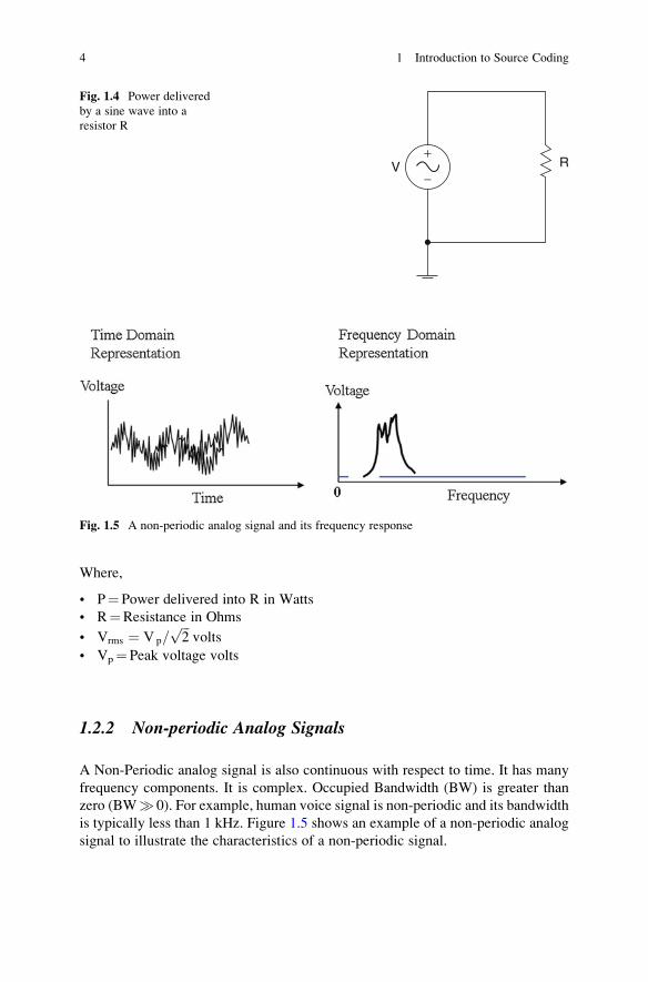
Where,
• P¼ Power delivered into R in Watts
• R¼Resistance in Ohms
• Vrms ¼ Vp=ffiffiffi2
pvolts
• Vp¼ Peak voltage volts
1.2.2 Non-periodic Analog Signals
A Non-Periodic analog signal is also continuous with respect to time. It has many
frequency components. It is complex. Occupied Bandwidth (BW) is greater than
zero (BW� 0). For example, human voice signal is non-periodic and its bandwidth
is typically less than 1 kHz. Figure 1.5 shows an example of a non-periodic analog
signal to illustrate the characteristics of a non-periodic signal.
V R+
−
Fig. 1.4 Power delivered
by a sine wave into a
resistor R
Fig. 1.5 A non-periodic analog signal and its frequency response
4 1 Introduction to Source Coding

1.2.3 Periodic Digital Signals
A periodic digital signal is continuous with respect to time. It has an infinite number
of harmonically related sinusoidal waveforms. For example a square wave, having
a 50 % duty cycle, is represented by a waveform as shown in Fig. 1.6a and its
spectral response in Fig. 1.6b. The square wave is described by the following time
domain equation:
V tð Þ ¼ Vp Sin ωtð Þ½ � þ Vp=3 Sin 3ωtð Þ½ � þ Vp=5 Sin 5ωtð Þ½ � þ . . . ð1:3Þ
Where,
• Vp¼ Peak voltage
• ω¼ 2πf• f¼ Frequency in Hz
Figure 1.6a shows the characteristics of the square wave and its spectral response
in Fig.1.6b. The spectral response is located in the horizontal axis and the peak
voltage is shown in the vertical axis.
From the above, we see that a digital signal has an infinite number of harmon-
ically related spectral components. Therefore, the occupied bandwidth is infinity.
We also note that the peak voltages are also related as follows:
V p1 ¼ 4V=π at ω Fundamentalð ÞV p3 ¼ 4V=3π at 3ω 3rd harmonic
� �V p5 ¼ 4V=5π at 5ω Fifth harmonicð ÞV p7 ¼ 4V=7π at 7ω 7th harmonic
� �
Furthermore, we note that the higher order spectral components are negligible.
Therefore, techniques such as filtering signal formatting etc. can be used to limit the
bandwidth. We shall revisit this again later in this chapter.
Next, let’s examine the power delivered into a resistor R, where the source is a
periodic square wave as shown in Figure 1.7. We know that a discrete time signal
has an infinite number of harmonically related sinusoidal waves. Therefore, the
Fig. 1.6 A periodic digital signal and its spectral components
1.2 Identification and Characterization of Input Signals 5
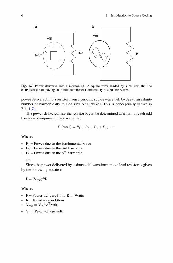
power delivered into a resistor from a periodic square wave will be due to an infinite
number of harmonically related sinusoidal waves. This is conceptually shown in
Fig. 1.7b.
The power delivered into the resistor R can be determined as a sum of each odd
harmonic component. Thus we write,
P totalð Þ ¼ P1 þ P3 þ P5 þ P7, . . . :
Where,
• P1¼ Power due to the fundamental wave
• P3¼ Power due to the 3rd harmonic
• P5¼ Power due to the 5th harmonic
etc.
Since the power delivered by a sinusoidal waveform into a load resistor is given
by the following equation:
P¼ (Vrms)2/R
Where,
• P¼ Power delivered into R in Watts
• R¼Resistance in Ohms
• Vrms ¼ Vp=ffiffiffi2
pvolts
• Vp¼ Peak voltage volts
V(t)
a b
V(t)
R=1 Rf=1/T
0 T
V
Fig. 1.7 Power delivered into a resistor. (a) A square wave loaded by a resistor. (b) The
equivalent circuit having an infinite number of harmonically related sine waves
6 1 Introduction to Source Coding

We write, for the square wave:
P1 ¼ V p1=ffiffiffi2
p� �2=R ¼ 4V=π
ffiffiffi2
p� �2=R Fundamentalð Þ
P3 ¼ V p3=ffiffiffi2
p� �2=R ¼ 4V=3π
ffiffiffi2
p� �2=R Third harmonicð Þ
P5 ¼ V p5=ffiffiffi2
p� �2=R ¼ 4V=5π
ffiffiffi2
p� �2=R Fifth harmonicð Þ
The total power will be,’
P totalð Þ ¼ 4V=πffiffiffi2
p� �2=Rþ ¼ 4V=3π
ffiffiffi2
p� �2=Rþ 4V=5π
ffiffiffi2
p� �2=Rþ . . .
¼ 8=πð Þ V=Rð Þ 1þ 1=9þ 1=25þ 1=49þ . . . :½ �
Which is an infinite series, Where,
1þ 1=9þ 1=25þ 1=49þ . . . :½ � ¼ π=8
Therefore, the total power is given by,
P totalð Þ ¼ V2=R ð1:4Þ
Problem 1.1
This problem verifies Fourier series.
Given:
• Square wave
• V¼ 10 V
• T¼ 1 ms.
Find:
(a) The spectral components of the square wave (up to the 9th)
(b) Show that the sum of all the spectral components in part (a) of this problem
approximates a square wave.
Solution:
(a) For the square wave we have: V¼ 10 V, f ¼1/T¼ 1/1 ms¼ 1 kHz. Therefore,
the spectral components are:
V1 ¼ 4V=π Sin 2π� 1000tð Þ ¼ 12:739Sin 2π� 1000tð Þ Fundamentalð ÞV3 ¼ 4V=3π Sin 2π� 3000tð Þ ¼ 4:246 Sin 2π� 3000tð Þ 3rdharmonic
� �V5 ¼ 4V=5π Sin 2π� 5000tð Þ ¼ 2:547Sin 2π� 5000tð Þ Fifth harmonicð ÞV7 ¼ 4V=7π Sin 2π� 7000tð Þ ¼ 1:819Sin 2π� 7000tð Þ 7thharmonic
� �V9 ¼ 4V=9π Sin 2π� 9000tð Þ ¼ 1:415Sin 2π� 9000tð Þ 9thharmonic
� �
(b) Use a summing amplifier to add the voltages having harmonically related
wave forms. The output voltage is given by:
Vo ¼ � V1 þ V3 þ V5 þ V7 þ V9½ � R2=R1ð Þ
1.2 Identification and Characterization of Input Signals 7

Where R1¼R2. The negative sign indicates voltage inversion. The circuit
was simulated by means of “Multisim”™. Notice that the output voltage
approximates a square wave only with five harmonic components. Closer
approximations can be achieved by adding more harmonic components.
V1R1
R1
R1
R2
Vo
Vo
R1
R1
R1Time
V9
V7
V5
V3
+−
+−
+−
+−
+−
+
−
1.2.4 A Non-periodic Digital Signals
In digital communications, data is generally referred to as a non-periodic digital
signal as shown in Fig. 1.8. The data has two values:
• Binary-1¼High, Period¼T
• Binary-0¼Low, Period¼T
• Known as Non-Return to Zero (NRZ) Data
It has many frequency components, which can be determined by means of
Fourier transform.
Fig. 1.8 A non-periodic
digital signal
8 1 Introduction to Source Coding

Data can be represented in two ways:
Time domain representation (Fig. 1.9a):
V tð Þ¼ V < 0 < t < T
¼ 0 elsewhereð1:5Þ
Frequency domain representation is given by: “Fourier Transform”:
V ωð Þ ¼ðT
0
V � e� jωtdt ð1:6Þ
V ωð Þj j ¼ VTSin ωT=2ð Þ
ωT=2
� �ð1:7Þ
P ωð Þ ¼ 1
T
� �V ωð Þj j2 ¼ V2T
Sin ωT=2ð ÞωT=2
� �2ð1:8Þ
This is plotted in Fig. 1.9b. The main lobe corresponds to the fundamental
frequency side lobes correspond to harmonic components. The bandwidth of the
power spectrum is proportional to the frequency.
The general equation for two sided response is given by:
V ωð Þ ¼ð1
�1V tð Þ � e� jωtdt ð1:9Þ
In this case, V(ω) is called two sided spectrum of V(t). This is due to both positive
and negative frequencies used in the integral. The function can be a voltage or a
current
Fig. 1.9 (a) Discrete time digital signal and (b) it’s one-sided power spectral density
1.2 Identification and Characterization of Input Signals 9

1.2.5 Clock and Data
Clock is a periodic square waveform. It has a 50 % duty cycle, where T is the period
of the waveform and f is the frequency. They are related by the following equation:
T ¼ Period ¼ 1= fcfc ¼ frequency
ð1:10Þ
In digital communications, the clock signal is used to:
• synchronize digital signals
• Upload and Download data
• Shift data serially
• Converts data into a parallel stream
• Converts data back to serial stream
• Etc.
Figure 1.10 shows the relationship between a clock and data. Data is the digital
information. It has two values:
• Binary-1¼High, Period¼T
• Binary-0¼Low, Period¼T
Data has several formats [5]:
• NRZ (Non-Return to Zero)
• RZ (Return to Zero)
• AMI (Alternate Mark Inversion)
• Etc.
For NRZ data, logic-1 and Logic-0 are represented by the entire duration of the
clock T. On the other hand, for Rz data, Logic 1 is represented by T/2 as shown in
Fig. 1.10. Logic changes are triggered either by the rising edge or the falling edge of
the clock. The bit rate is governed by the clock rate. For example, a 10 kb/s NRZ
data requires a 10 kHz clock.
Fig. 1.10 Relationship between clock and data
10 1 Introduction to Source Coding
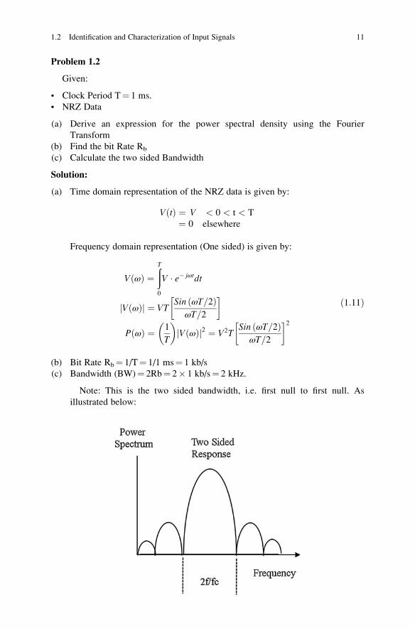
Problem 1.2
Given:
• Clock Period T¼ 1 ms.
• NRZ Data
(a) Derive an expression for the power spectral density using the Fourier
Transform
(b) Find the bit Rate Rb
(c) Calculate the two sided Bandwidth
Solution:
(a) Time domain representation of the NRZ data is given by:
V tð Þ ¼ V < 0 < t < T
¼ 0 elsewhere
Frequency domain representation (One sided) is given by:
V ωð Þ ¼ðT
0
V � e� jωtdt
V ωð Þj j ¼ VTSin ωT=2ð Þ
ωT=2
� �
P ωð Þ ¼ 1
T
� �V ωð Þj j2 ¼ V2T
Sin ωT=2ð ÞωT=2
� �2ð1:11Þ
(b) Bit Rate Rb¼ 1/T¼ 1/1 ms¼ 1 kb/s
(c) Bandwidth (BW)¼ 2Rb¼ 2� 1 kb/s¼ 2 kHz.
Note: This is the two sided bandwidth, i.e. first null to first null. As
illustrated below:
1.2 Identification and Characterization of Input Signals 11
1.3 Noise
1.3.1 Background
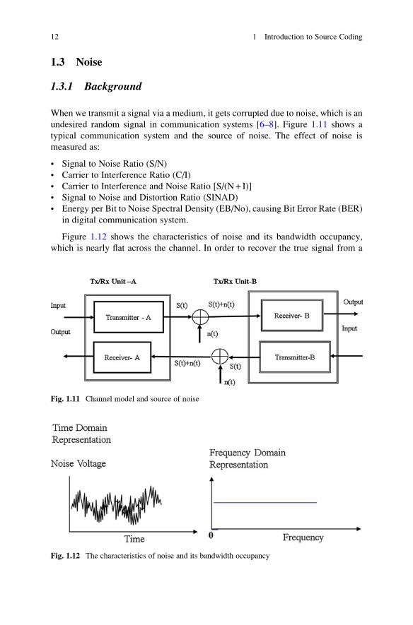
When we transmit a signal via a medium, it gets corrupted due to noise, which is an
undesired random signal in communication systems [6–8]. Figure 1.11 shows a
typical communication system and the source of noise. The effect of noise is
measured as:
• Signal to Noise Ratio (S/N)
• Carrier to Interference Ratio (C/I)
• Carrier to Interference and Noise Ratio [S/(N + I)]
• Signal to Noise and Distortion Ratio (SINAD)
• Energy per Bit to Noise Spectral Density (EB/No), causing Bit Error Rate (BER)
in digital communication system.
Figure 1.12 shows the characteristics of noise and its bandwidth occupancy,
which is nearly flat across the channel. In order to recover the true signal from a
Fig. 1.11 Channel model and source of noise
Fig. 1.12 The characteristics of noise and its bandwidth occupancy
12 1 Introduction to Source Coding
noisy environment, we need to understand the source of noise and its
characteristics.
The source of noise can be:
• Natural: Thermal noise and Shot noise.
• Unintentional: Co-Channel and Adjacent channel Interference (CCI and ACI)
from cellular communication
• Intentional: Jamming from an adversary
A brief description of some of these noise parameters are described below:
1.3.2 Thermal Noise
Thermal noise is generated by the random motion of charge carriers inside an
electrical conductor. The power spectral density is flat throughout the frequency
spectrum. See Fig. 1.12. For this reason, it is also known as “white”. The amplitude
of thermal noise also exhibits a Gaussian probability density function. As a result, a
communication channel affected by thermal noise is often modeled as an Additive
White Gaussian noise (AWGN).
The root mean square (RMS) voltage due to thermal noise, generated in a
resistance R, is given by:
vn ¼ffiffiffiffiffiffiffiffiffiffiffi4kTB
pð1:12Þ
Where
• k¼ Boltzmann’s constant (joules per kelvin) and
• T¼Absolute temperature (kelvin).
• B¼Noise bandwidth
1.3.3 Shot Noise
Shot noise in electronic devices is due to random fluctuations of charges. The flow
of these charges is relatively continuous but they arrive at random, causing a
fluctuation in current flow. The root-mean-square value of the shot noise current
in is given by the Schottky formula
in ¼ffiffiffiffiffiffiffiffiffiffi2iqB
pð1:13Þ
Where
• i¼Current
• q¼Electron charge
• B¼Bandwidth in hertz.
1.3 Noise 13

1.4 Interference
1.4.1 Co-Channel Interference
In cellular communications, frequencies are reused in different cells, which mean
that another mobile can use the same frequency from a distant location. This is
known as “Frequency Reuse” [2, 4], Frequency reuse enhances channel capacity.
This is accomplished at the expense of unintentional interference, which is also
known as “Co-channel Interference or Carrier to Interference (C/I)].
As an illustration, we consider Fig. 1.13, where the same frequency is used in
Cell-A and Cell-B. Therefore, a mobile communicating with Cell-A will also
receive the same frequency from the distant Cell-B. This is analogous to the
“Near-Far” problem, causing co-channel interference. We use the following
method to determine this interference.
Let,
RSLA¼Received signal level at the mobile from Cell -A
dA¼Distance between the mobile and Cell-A
RSLB¼The received signal level at the mobile from Cell -B
dB¼Distance between the mobile and Cell-B
γ¼ Path loss exponent
Then we can write,
RSLA / dAð Þ�γ
RSLB / dBð Þ�γ ð1:14Þ
Where,
• RSL¼Received signal level
• d¼Distance between the transmitter and the receiver
• γ¼Received signal decay constant
The ratio of the signal strengths at the mobile will be:
RSLARSLB
¼ dAdB
� ��γ
¼ dBdA
� �γ
ð1:15Þ
Fig. 1.13 Carrier to Interference ratio (C/I) due to a single interferer
14 1 Introduction to Source Coding
In the above equation, RSLA is the RF signal received from the serving cell.
Therefore, this is the desired signal and we redefine this signal as the carrier signal
power C. We also assume that the mobile is at the cell edge from the serving cell-A,
which is the cell radius R (dA¼R). On the other hand, RSLB is the undesired signal
received from CellB and we redefine this signal as the interference signal power I.
The corresponding interference distance dB¼D; D being the reuse distance. There-
fore, above equation can be written as a carrier to interference ratio (C/I), due to a
single interferer, as:
C
I¼ D
R
� �γ
ð1:16Þ
In decibel, it can be written as:
C
IdBð Þ ¼ 10Log
D
R
� �γ
ð1:17Þ
Where,
• C¼ Signal power from the serving carrier
• I¼ Signal power from the interferer
• γ¼Received signal decay constant
• R¼Cell radius
• D¼Reuse distance
1.4.2 C/I Due to Multiple Interferers
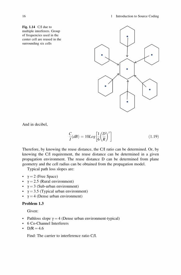
In hexagonal cellular geometry, each hexagonal cell is surrounded by six hexagons
as shown in Fig. 1.14. Therefore, in a mature cellular system, there can be six
primary interferers. The total interference from all six interferers will be [2, 4]:
6RSLB / dBð Þ�γ
or
RSLB / 1
6dBð Þ�γ
ð1:18Þ
Therefore, the effective interference ratio is:
C
I¼ RSLA
RSLB¼ 1
6
dAdB
� ��γ
¼ 1
6
dBdA
� �γ
¼ 1
6
D
R
� �γ
1.4 Interference 15
And in decibel,
C
IdBð Þ ¼ 10Log
1
6
D
R
� �γ� �ð1:19Þ
Therefore, by knowing the reuse distance, the C/I ratio can be determined. Or, by
knowing the C/I requirement, the reuse distance can be determined in a given
propagation environment. The reuse distance D can be determined from plane
geometry and the cell radius can be obtained from the propagation model.
Typical path loss slopes are:
• γ¼ 2 (Free Space)
• γ¼ 2.5 (Rural environment)
• γ¼ 3 (Sub-urban environment)
• γ¼ 3.5 (Typical urban environment)
• γ¼ 4 (Dense urban environment)
Problem 1.3
Given:
• Pathloss slope γ¼ 4 (Dense urban environment-typical)
• 6 Co-Channel Interferers
• D/R¼ 4.6
Find: The carrier to interference ratio C/I.
Fig. 1.14 C/I due to
multiple interferers. Group
of frequencies used in the
center cell are reused in the
surrounding six cells
16 1 Introduction to Source Coding

Solution:
C
IdBð Þ ¼ 10Log
1
6
D
R
� �γ� �
With γ¼ 4 and D/R¼ 4.6, we obtain:
C/I ~ 18 dB.
1.4.3 The Effect of Noise in Communication Channelsand Shannon’s Capacity Theorem
The effect of noise on communication channel was best described by Claude
Shannon [1]. Shannon’s capacity theorem states that, when transmitting a signal
in the presence of noise, we need to ensure that the signal power is greater than the
noise power, so that the signal can be recovered without an error. Shannon showed
that, in a noisy environment, the maximum bit rate that can be achieved is given by
the following formula:
C ¼ WLog2 1þ S
N
� �bits=s: ð1:20Þ
Where,
• C¼Channel capacity (bits/s)
• W¼Bandwidth in Hz
• S/N¼ Signal to Noise Ratio
Since the noise power is proportional to the bandwidth, we write:
• N¼No W
• No¼Noise spectral density at room temperature
Therefore, we can write,
C ¼ WLog2 1þ S
N
� �bits=s:
C ¼ WLog2 1þ S
N0W
� �bits=s:
Since C¼Bit rate, we define C¼R (b/s) and express the capacity theorem as
follows:
C ¼ WLog2 1þ S
N0W
� �bits=s:
OR
R
W¼ Log2 1þ S
N0W
� �bits=s per channel
ð1:21Þ
1.4 Interference 17

The Ratio R/W is Known As “Channel Capacity, which is a function of S/N. This is
plotted in Fig. 1.15.
We Observe the Following:
• To increase the capacity we need more S/N ratio
• More S/N ratio can be achieved by:
– Increasing the signal power
– Reducing the noise
– Defeating the noise by means of “Error Control Coding”
• However, there is a diminishing return, requiring a compromise between several
parameters, e.g., Available bandwidth, Forward Error Control Coding, Modula-
tion etc. These topics will be discussed in this series of books.
1.5 Measurement and Quantification of Signals
Measurement of Information is a discipline that quantifies information. We need
this because the transmission medium is limited. Information can be quantified by
means of:
• Decimal System (Analog Info.)
• Binary System (Digital Info.)
Both systems are equally good and widely used to quantify information for
further processing.
0.1
1
10
100
-10 0 10 20 30 40 50
SNR (dB)
R/W
(b
its/
Hz/
Sec
) Un-Realizable Region
Realizable Region
Fig. 1.15 Channel capacity
as a function of S/N
18 1 Introduction to Source Coding

1.5.1 Decimal System
In decimal system, the information is quantified as:
N ¼ 10m
Where, m ¼ 1, 2, 3, . . . :ð1:22Þ
As a result, the value of N increases rapidly as a power of 10. This is given by:
N ¼ 100, 101, 102, 103, 104, 105, . . .¼ 1, 10, 100, 1000, 10000, 100000, . . . :
Since the number N increases rapidly, it is inconvenient. As such we use Logarith-
mic Scale with a base of 10:
M ¼ Log10 Nð Þ¼ 0, 1, 2, 3, . . .
ð1:23Þ
Where N¼¼1, 10, 100, 1000, . . .This number (M) is Small and convenient to use.
1.5.2 Binary System
In Binary system, the information is quantified as:
N ¼ 2m ð1:24Þ
Where m¼ 1, 2, 3, . . ..As a result, the value of N increases rapidly:,
N ¼ 20, 21, 22, 23, 24, 25, . . .¼ 1, 2, 3, 4, 8, 16, 32, . . .
ð1:25Þ
Since the number N also increases rapidly, it is inconvenient. As such we use
Logarithmic Scale with a base of 2:
M ¼ Log2 Nð Þ¼ 0, 0:301, 0:602, 0:903, . . .
ð1:26Þ
Where, N¼ 1, 2, 4, 8, . . .This number (M) is also Small and convenient to use.
The relationship between binary and decimal systems is given by:
1.5 Measurement and Quantification of Signals 19
Log2 Nð Þ ¼ Log10 Nð ÞLog10 2ð Þ ¼ 3:32 Log10 Nð Þ
Problem 1.4:
Given:
• 26 Letters in English Language: A, B, . . . Z• Each Letter is Equally Likely
Find: The Average Number of Bits Needed to Transmit a Single Letter
Solution:
m ¼ Log10 26ð Þ½ �= Log10 2ð Þ½ � ¼ 4:7 ’ 5
Therefore, we need 5 bits per letter.
1.6 Conclusions
• Source Coding defined
• Reviewed Signals and spectra
• Discussed Signal to Noise Ratio and Effects of Noise on Communication
Circuits
• Shannon’s Capacity Theorem indicates that there is a diminishing return
• In light of Shannon’s capacity theorem, it may be concluded that communication
systems engineering is partly science, partly engineering and mostly art. It has to
adapt to changing technology such as channel coding, modulation, Frequency
reuse and C/I management etc.
References
1. C.E. Shannon, A mathematical theory of communication. Bell System Technical Journal 27,379–423 (1948). 623–656
2. William C.Y. Lee, Mobile cellular telecommunications systems. McGraw-Hill Book Company,
New York.
3. Theodore S. Rappaport. Wireless communications. Pearson Education, ISBN: 81-7808-648 -4, 2002.
4. S. Faruque, Cellular mobile systems engineering, Artec House Inc., ISBN: 0-89006-518-7,
1996.
5. DR. Smith, Digital transmission systems, Van Nostrand Reinhold Co. ISBN: 0442009178,
1985.
6. C.D.Motchenbacher, J.A. Connelly,Low-noise electronic system design (Wiley,NewYork, 1993)
7. L.B. Kish, C.G. Granqvist, Noise in nanotechnology. Microelectronics Reliability 40(11),1833–1837 (2000). doi:10.1016/S0026-2714(00)00063-9
8. A. Steinbach, J. Martinis, M. Devoret, Observation of hot-electron shot noise in a metallic
resistor. Phys. Rev. Lett. 76(20), 38.6–38.9 (1996). doi:10.1103/PhysRevLett.76.38.
Bibcode:1996PhRvL..76. . .38M
20 1 Introduction to Source Coding

Chapter 2
Baseband Filters: Active RC Filters
Topics
• Introduction
• Voltage and Current Sources
• Voltage to Current Transducers
• Amplifiers and Integrators
• Simulation of Inductors
• Active Filter Design based on simulated inductors
• Higher Order Active Filters Based on Simulated Inductors
2.1 Introduction
In telecommunications, voice transmission is a primary service (e.g., digital tele-
phones, cellular communications). Since human voice occupies a spectrum from
300 Hz to 3.4 kHz, a baseband filter is used to pass this frequency band and reject all
others. To realize these filters, the traditional networks used inductors, capacitors
and resistors to perform analog functions [1, 2]. In this frequency region, the
inductors are heavy and expensive. Efforts have been made to replace them by
networks consisting of active elements, capacitors and resistors [3, 4]. This devel-
opment was very successful and active RC networks are now widely used by
industry.
In an attempt to contribute in opening the way for scholarly research in the area
of analog low frequency simulation on a chip, this text develops first the idea of
transconductance models of network building blocks known from the analog world:
amplifiers with prescribed gain integrators and inductors. All these networks are
derived from their continuous time counterparts [5, 6]. It is assumed that the student
is familiar with the basic concept of circuit theory.
© Springer International Publishing Switzerland 2015
S. Faruque, Radio Frequency Source Coding Made Easy, SpringerBriefsin Electrical and Computer Engineering, DOI 10.1007/978-3-319-15609-5_2
21

2.2 Voltage to Current Source
The most commonly used voltage source is given in Fig. 2.1a where Rs is the source
resistance. The voltage V is ideal which means that it is independent of loading. The
equivalent current source is given in Fig. 2.1b in which
I ¼ V=R ð2:1Þ
where the generated current I is also ideal.
2.3 Voltage to Current Transducer (Transconductance)
A Transconductance is a two-port network whose output current is proportional to
the input voltage. The symbolic representation is given in Fig. 2.2 in which gm is the
transconductance.
R
RV
I
Va b
I =V/R
Fig. 2.1 (a) A voltage
source, (b) A current source
22 2 Baseband Filters: Active RC Filters

The input–output relation is expressed as
I0 ¼ gm v1 � V2ð Þ ð2:2Þ
The element is also known as “Voltage to Current Transducer” (VCT).
2.4 Amplifiers
2.4.1 Differential Amplifier
A Transconductance, when loaded by a resistance, becomes an amplifier. Thus
consider the Transconductance circuit as shown in Fig. 2.3a where R2 is the load
resistance. The current Equation of this circuit can be written as
V1
Io = gm (V1-V2)V2
Io
Fig. 2.2 Symbolic
representation of a
transconductance
V1
Io
V2
R2
Vo
Vo
R1
a b R2
V1
V2
R1R2
Fig. 2.3 (a) A differential transconductance amplifier and (b) its active realization by means of
operational amplifier
2.4 Amplifiers 23

Io ¼ gm V1 � V2ð Þ ¼ �V0=R2 ð2:3Þ
The differential voltage gain is therefore
AV ¼ V0= V1 � V2ð Þ ¼ �gmR2 ð2:4Þ
The polarity of the output voltage can be reversed simply by reversing the input
voltages:
AV ¼ V0= V2� V1ð Þ ¼ gmR2 ð2:5Þ
Now consider the OpAmp realization of the differential amplifier as shown in
Fig. 2.3b. The Voltage gain of this amplifier is given by,
Av ¼ Vo= V1 � V2ð Þ ¼ �R2=R1 ð2:6Þ
Comparing this with the transconductance model, we have,
gm ¼ 1=R1 ð2:7Þ
2.4.2 Inverting Amplifier
Figure 2.4 shows an inverting transconductance amplifier and its active realization
by means of operational amplifier. From the transconductance amplifier, we obtain,
Io ¼ gmVin ¼ �V0=R2 ð2:8Þ
The voltage gain is therefore
AV ¼ V0=Vinj ¼ �gmR2 ð2:9Þ
V in
Io = gm Vin
VoVin
R1
R2
a b
R2
Fig. 2.4 (a) An inverting transconductance amplifier and (b) its active realization by means of
operational amplifier. Operational amplifier
24 2 Baseband Filters: Active RC Filters

Now consider the OpAmp realization of the inverting amplifier as shown in
Fig. 2.4b. The voltage gain of this amplifier is given by,
Av ¼ Vo=Vin ¼ �R2=R1 ð2:10Þ
Comparing this with the transconductance model, we have,
gm ¼ 1=R1 ð2:11Þ
2.4.3 Non-inverting Amplifier
A non-inverting amplifier can be realized as shown in Fig. 2.5. From the transcon-
ductance model, the voltage gain of this amplifier is,
Av ¼ gmR2
where gm¼ 1/R2.
From the OpAmp realization of the non-inverting amplifier as shown in
Fig. 2.5b, the Voltage gain becomes,
Av ¼ Vo=Vin ¼ R2=R1 ð2:12Þ
Comparing this with the transconductance model, we have,
gm ¼ 1=R1 ð2:13Þ
1mMho
a bIo = gm Vin
Vo
Vin
R1
R2
R2
R1
R2
V in
Fig. 2.5 (a) A non-inverting transconductance amplifier and (b) its active realization by means of
operational amplifier
2.4 Amplifiers 25

2.5 Integrators Based on Transconductances
A Transconductance, when loaded by a capacitor, becomes an integrator. Figure 2.6
shows an Inverting transconductance integrator and its active realization by means
of an Operational Amplifier. The corresponding transfer Functions are:
T sð Þ ¼ V0=Vin ¼ �gm=sC ð2:14Þ
T sð Þ ¼ V0=Vin ¼ �1= sCRð Þ ð2:15Þ
where gm¼ 1/R.
Next, consider a non-inverting transconductance integrator and its active reali-
zation by means of Operational amplifier as shown in Fig. 2.7. The voltage Transfer
functions of these integrators are respectively,
T sð Þ ¼ gm=sC ð2:16Þ
T sð Þ ¼ 1= sCRð Þ ð2:17Þ
where gm¼ 1/R.
2.6 Differential Integrators
A differential integrator, based on transconductance, is given in Fig. 2.8a. The
output voltage transfer function is given by
V in
a bVo
C
Io = gm Vin
VoVin
R
C
Fig. 2.6 (a) An inverting transconductance integrator and (b) its active realization by means of
OpAmp
26 2 Baseband Filters: Active RC Filters
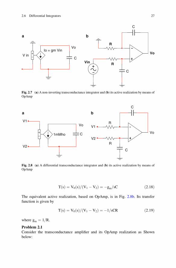
T sð Þ ¼ V0 sð Þ= V1 � V2ð Þ ¼ �gm=sC ð2:18Þ
The equivalent active realization, based on OpAmp, is in Fig. 2.8b. Its transfer
function is given by
T sð Þ ¼ V0 sð Þ= V1 � V2ð Þ ¼ �1=sCR ð2:19Þ
where gm ¼ 1=R.
Problem 2.1
Consider the transconductance amplifier and its OpAmp realization as Shown
below:
V in
a b
Vo
C
Io = gm VinVo
Vin
R
R
C
C
Fig. 2.7 (a) A non-inverting transconductance integrator and (b) its active realization by means of
OpAmp
Vo
R
1mMho C
VoV1
a b
V2R
C
C
V1
V2
Fig. 2.8 (a) A differential transconductance integrator and (b) its active realization by means of
OpAmp
2.6 Differential Integrators 27

V in
Vo
R2Io = gm1 Vin Vo
Vin
R1
R2
(a) Design the transconductance amplifier to deliver a voltage gain of 20 dB.
(b) Design the OpAmp amplifier to deliver a voltage gain of 20 dB.
Solution to Problem 2.1:
(a) The voltage gain is given by
Av ¼ �gm1R2
For Av dBð Þ ¼ 20dB, Av v=vð Þ ¼ 1020=20 ¼ 10v=vAvj j ¼ gm1R2j j ¼ 10. Let R2¼ 10k. Then, gm1¼ 1 mMho.
(b) For the OpAmp amplifier, the voltage gain is given by,
Av ¼ �Vo=Vin ¼ �R2=R1 ¼ �10. Therefore, the voltage gain in dB is
given by:
Av dBð Þj j ¼ 20Log 10ð Þ ¼ 20dB:
Problem 2.2
Consider the transconductance integrator and its OpAmp realization as shown
below:
V in
Vo
C
Io = gm Vin Vo
Vin
R
C
28 2 Baseband Filters: Active RC Filters

(a) Design the transconductance integrator to deliver a time constant of 1 ms.
(b) Design the OpAmp integrator to deliver a time constant of 1 ms.
Solution 2.2:
From the transconductance circuit we obtain the nodal equation
gmVin ¼ �V0sC where s ¼ jω, ω ¼ 2π f, f¼ Frequency
The voltage transfer function is given by,
T sð Þ ¼ Vo=Vin ¼ �gm=sC
From the OpAmp integrator, we have,
T sð Þ ¼ Vo=Vin ¼ �1=sCR
Therefore, For R¼ 1/gm, both the integrators are functionally identical.
The 1 ms time constant, can be realized as:
τ ¼ RC ¼ C=gm ¼ 1ms R ¼ 103Ohm, C ¼ 10�6 F, gm ¼ 10�3Mho� �
2.7 Simulation of Grounded Inductor
The transconductance models of integrators, developed in the previous chapter, will
now be used to simulate various building blocks such as grounded inductors,
floating inductors, LC sections etc. Various second order and more complex filter
functions can be realized by using these building blocks.
A grounded inductor can be realized by means of two transconductances, as
shown in Fig. 2.9.
From Fig. 2.9 we derive,
I1 ¼ gm1V2 ð2:20Þ
I2 ¼ gm2V1 ¼ V2sC2 ð2:21Þ
From (2.21) V2 we get
V2 ¼ gm2V1=sC2 ð2:22Þ
Substituting (2.22) into (2.20), for V2, I1 can be written as
I1 ¼ gm1gm2V1=sC2 ð2:23Þ
Solving for the input impedance Zin¼V1/i1 we obtain
2.7 Simulation of Grounded Inductor 29

Zin ¼ V1=I1 ¼ sC2=gm1gm2 ð2:24Þ
Thus the element simulates a grounded inductor of value
L ¼ C2=gm1gm2 ð2:25Þ
2.8 Simulation of Floating Inductor
A floating inductor can be represented by a two-port network comprising transcon-
ductances as shown in Fig. 2.10.
The impedance of a floating inductor is given by,
ZL ¼ \ sL ¼ V1 � V3ð Þ=I ð2:26Þ
where,
• s¼ jω, ω¼ 2πf, f¼ frequency
• V1�V3 is the voltage across the inductor, and
• I is the current through the inductor
From the transconductance model of the floating inductor we have,
I1 ¼ gm1V2 ð2:27Þ
I2 ¼ gm2 V1 � V3ð Þ ¼ sC2V2 ð2:28Þ
I1 = gm1 V2 I2 = gm2 V1
V2
C2
V1V1
LI1 I2I1
L=C2/(gm1 gm2)
Fig. 2.9 A grounded inductor and its transconductance model
30 2 Baseband Filters: Active RC Filters

I3 ¼ gm3V2 ð2:29Þ
From (2.28) we get,
V2 ¼ gm2 V1 � V3ð Þ=sC2 ð2:30Þ
Substituting (2.30) for V2 in (2.27) and (2.29), we get,
I1 ¼ gm1gm2 V1 � V3ð Þ=sC2 and ð2:31Þ
I3 ¼ gm3gm2 V1� V3ð Þ=sC2 ð2:32Þ
The condition for an equivalent inductor is
gm1 ¼ gm3 ð2:33Þ
Therefore,
I ¼ gm1gm2 V1 � V3ð Þ=sC2
ZL ¼ V1 � V3ð Þ=I ¼ sC2=gm1gm2
ð2:34Þ
The value of the inductor is then
L ¼ C2=gm1gm2 ð2:35Þ
where gm1 ¼ gm3.
LV1 V3
I1 = gm1 V2V1
I2 = gm2(V1-V3) V2
C2I1 I2
I3 = gm3 V2V3
I3
Fig. 2.10 A floating inductor and its transconductance model
2.8 Simulation of Floating Inductor 31

2.9 Second Order Filters: The Biquad
A biquad (bi-quadratic) filter is a second order filter which can provide various
second order transfer functions. A biquad transfer function is the one whose
numerator and denominator polynomials are quadratic in nature. This section will
briefly review some of the most useful second order transfer functions derived from
the general biquad transfer function as given below:
T sð Þ ¼s2 þ ωz
Qz
� �sþ ωz
s2 þ ω pQp
� �sþ ωp
ð2:36Þ
where,
s¼ jω Laplace transform variable
ωz¼ zeroes of the transfer function
ωp¼ poles of the transfer function
Qz¼ quality factor of the zeroes
Qp¼ quality factor of the poles
Zeros are described by the numerator polynomial and Poles are described by the
denominator polynomial. Most frequently used transfer functions are described in
the following:
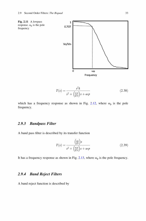
2.9.1 Lowpass Filter
A Lowpass filter is described by the following transfer function:
T sð Þ ¼ ωz
s2 þ ω pQ p
� �sþ ω p
ð2:37Þ
The frequency response is shown in Fig. 2.11. The pole frequency ωp is measured
when the voltage transfer function |T(s) is 70 % of its maximum value.
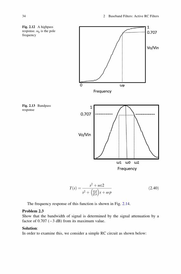
2.9.2 High Pass Filter
A high pass filter is described by its transfer function as shown below:
32 2 Baseband Filters: Active RC Filters
T sð Þ ¼ s2k
s2 þ ω pQ p
� �sþ ω p
ð2:38Þ
which has a frequency response as shown in Fig. 2.12, where ωp is the pole
frequency.
2.9.3 Bandpass Filter
A band pass filter is described by its transfer function
T sð Þ ¼ωzQz
� �s
s2 þ ω pQ p
� �sþ ω p
ð2:39Þ
It has a frequency response as shown in Fig. 2.13, where ωp is the pole frequency.
2.9.4 Band Reject Filters
A band reject function is described by
Fig. 2.11 A lowpass
response. ωp is the pole
frequency
2.9 Second Order Filters: The Biquad 33
T sð Þ ¼ s2 þ ωz2
s2 þ ω pQ p
� �sþ ω p
ð2:40Þ
The frequency response of this function is shown in Fig. 2.14.
Problem 2.3
Show that the bandwidth of signal is determined by the signal attenuation by a
factor of 0.707 (�3 dB) from its maximum value.
Solution:
In order to examine this, we consider a simple RC circuit as shown below:
Fig. 2.13 Bandpass
response
Fig. 2.12 A highpass
response. ωp is the pole
frequency
34 2 Baseband Filters: Active RC Filters

R
C
Vo
Vin
The voltage transfer function is given by,
T sð Þ ¼ Vo=Vin ¼ 1= 1þ jωRCð Þ ¼ 1= 1þ jω=ω p
� �
The magnitude response is given by,
T sð Þj j ¼ 11=��1þ ω=ω p
� �2�1=2where ω¼ 2πf, f¼ frequency and ωp¼ 1/RC.
• For ω/ωp¼ 0: |T(s)|¼ 1 or 20Log(1)¼ 0 dB
• For ω/ωp¼ 1: |T(s)|¼ 1/(2)1/2¼ 0.707 or 20Log(0.707)¼�3 dB
• For ω/ωp¼ Infinity: |T(s)|¼ 0
Fig. 2.14 Band reject
response
2.9 Second Order Filters: The Biquad 35

The frequency response is given below.
2.10 Active Filters Based on Simulated Inductors
Active filter design, based on simulated inductors, is a three step process:
• It begins with a LC prototype filter as shown in Fig. 2.15a.
• Next, the inductor is replaced by its transconductance model as shown in
Fig. 2.15b, where the inductor model is shown in the dotted box.
• Finally, the transconductance model is replaced by its active equivalent circuit as
shown in Fig. 2.15c.
2.10.1 LC Prototype Filter
We begin with the LC prototype filter as shown in Fig. 2.15a.
The nodal equation is given by,
V1 G1 þ sC1 þ 1=sL1ð Þ ¼ G1Vin ð2:41Þ
where G1¼ 1/R1. The voltage transfer function is given by
H sð Þ ¼ V1
Vin
¼ s= R1C1ð Þs2 þ s C1=R1ð Þ þ 1=L1C1
ð2:42Þ
which is a Bandpass function (see the previous section)? Comparing the denomi-
nator with the following characteristics equation:
36 2 Baseband Filters: Active RC Filters

s2 þ s C1=R1ð Þ þ 1=L1C1 ¼ s2 þ s ωo=Qð Þþωo2 ð2:43Þ
We obtain,
ωo ¼ 1=L1C1ð Þ1=2 ð2:44Þ
Q ¼ R1 C1=L1ð Þ1=2 ð2:45Þ
where ωo is the center frequency and Q is the quality factor, which is also known as
selectivity.
2.10.2 Transconductance Model of the Prototype Filter
Next, consider the transconductance model of the LC prototype filter as shown in
Fig. 2.15b. Here, the simulated inductor L1 is given by:
V2V1
I1 = gm1 V2 I2 = gm2 V1V2
C2
V1
I1 I2
R1
Vin
R1a b
c
VinV1
C1L1
C1
C1C2
R1
R1
Rm1
Rm1
Rm2Vin
C1
Fig. 2.15 (a) An LC prototype filter, (b) its transconductance model and (c) the corresponding
active realization by means of OpAmps
2.10 Active Filters Based on Simulated Inductors 37
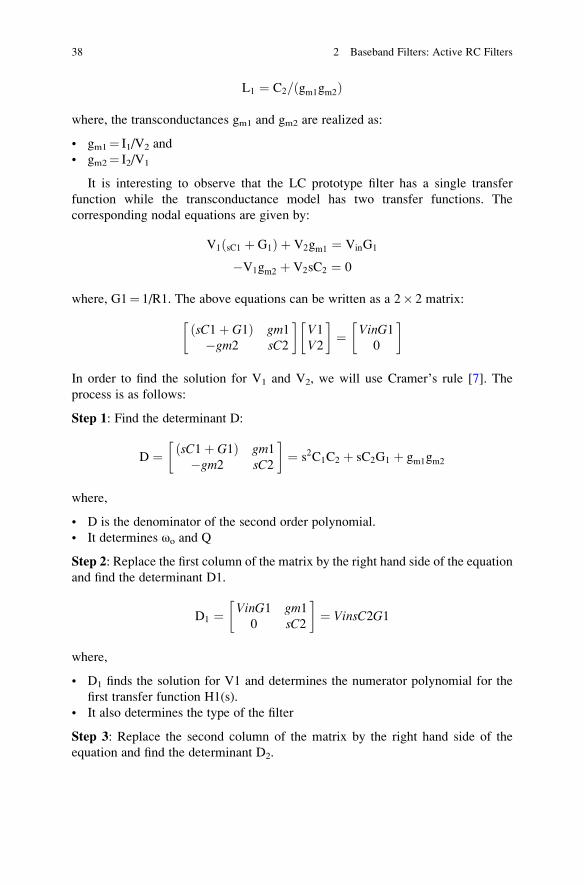
L1 ¼ C2= gm1gm2ð Þ
where, the transconductances gm1 and gm2 are realized as:
• gm1¼ I1/V2 and
• gm2¼ I2/V1
It is interesting to observe that the LC prototype filter has a single transfer
function while the transconductance model has two transfer functions. The
corresponding nodal equations are given by:
V1 sC1 þ G1ð Þ þ V2gm1 ¼ VinG1
�V1gm2 þ V2sC2 ¼ 0
where, G1¼ 1/R1. The above equations can be written as a 2� 2 matrix:
sC1þ G1ð Þ gm1�gm2 sC2
� V1V2
� ¼ VinG1
0
�
In order to find the solution for V1 and V2, we will use Cramer’s rule [7]. The
process is as follows:
Step 1: Find the determinant D:
D ¼ sC1þ G1ð Þ gm1�gm2 sC2
� ¼ s2C1C2 þ sC2G1 þ gm1gm2
where,
• D is the denominator of the second order polynomial.
• It determines ωo and Q
Step 2: Replace the first column of the matrix by the right hand side of the equation
and find the determinant D1.
D1 ¼ VinG1 gm10 sC2
� ¼ VinsC2G1
where,
• D1 finds the solution for V1 and determines the numerator polynomial for the
first transfer function H1(s).
• It also determines the type of the filter
Step 3: Replace the second column of the matrix by the right hand side of the
equation and find the determinant D2.
38 2 Baseband Filters: Active RC Filters

D2 ¼ sC1þ G1ð Þ VinG1�gm2 0
� ¼ Vingm1gm2
where,
• D2 finds the solution for V2 and determines the numerator polynomial for the
second transfer function H2(s).
• It also determines the type of the filter
Step 4: Find the Solutions for V1 and V2:
The solution for V1 and V2 are:
V1 ¼ D1=D ¼ VinsC2G1= s2C1C2 þ sC2G1 þ gm1gm2ð ÞV2 ¼ D2=D ¼ Vingm1gm2= s2C1C2 þ sC2G1 þ gm1gm2ð Þ
The corresponding voltage transfer functions are:
H1 sð Þ ¼ V1=Vin ¼ sC2G1= s2C1C2 þ sC2G1 þ gm1gm2ð ÞH2 sð Þ ¼ V2=Vin ¼ gm1gm2= s2C1C2 þ sC2G1 þ gm1gm2ð Þ
Therefore, H1(s) is a bandpass function and H2(s) is a lowpass function. Comparing
the denominator with the characteristics equation s2 þ s ωo=Qð Þ þ ωo2, we obtain,
• ω0 ¼ gm1gm2ð Þ= C1C2ð Þ½ �1=2 ð2:46Þ• Q ¼ R1gm C1=C2ð Þ1=2 ð2:47Þ• gm1 ¼ gm2 ¼ gm
2.10.3 RC Active Equivalent of the LC Prototype Filter
Finally, the equivalent active RC filter is obtained by replacing the transcon-
ductance integrators by their equivalents as developed earlier. This is shown in
Fig. 2.15c.
• The first stage has a non-inverting integrator and an inverting amplifier. The
non-inverting integrator has a pair of 1k resistors, realizing gm1 (1 mMho). This
stage is realized by means of a differential transconductance integrator shown in
the figure. The amplifier stage has a pair of 10k resistors, realizing a d.c. voltage
gain of �1 (V1/Vin¼ 10k/10k¼� 1).
• The second stage is an inverting integrator. This stage is realized by means
of an inverting integrator. Realizing the second transconductance gm2
(gm2¼ 1 mMho).
2.10 Active Filters Based on Simulated Inductors 39

The voltage transfer functions are:
H1 sð Þ ¼ V1=Vin ¼ sC2G1= s2C1C2 þ sC2G1 þ 1=Rm1Rm2ð ÞH1 sð Þ ¼ V2=Vin ¼ gm1gm2= s2C1C2 þ sC2G1 þ 1=Rm1Rm2ð Þ
Therefore, H1(s) is a bandpass function and H2(s) is a lowpass function. Comparing
the denominator with the characteristics equation s2 + s(ωo/Q) + ωo2, we obtain,
• ω0 ¼ 1= Rm1Rm2C1C2ð Þ�1=2• Q ¼ R1=Rm C1=C2ð Þ1=2
• gm1 ¼ gm2 ¼ gm¼1=Rm
Problem 2.4
Consider the LC prototype as shown in Fig. 2.15a with the following design
parameters:
• R1 ¼ 10k
• C1 ¼ 1nF
• L1 ¼ 0:81H
Find: fo and Q
Solution:
ωo ¼ 1=L1C1ð Þ1=2
fo ¼ 1=2πð Þ�1= 0:81H� 1nFð Þ1=2 ¼ 5, 594:971Hz
Q ¼ R1 C1=L1ð Þ1=2 ¼ 104 � 10�9=0:81� �1=2 ¼ 0:351364
Problem 2.5Consider the transconductance model of the LC prototype filter as shown in
Fig. 2.15b and calculate the values of transconductances and capacitors.
Solution:The inductor is given by the following equation:
L1 ¼ C2=gm1gm2 ¼ 0:81H
The value of the inductor can be realized by means of C2, gm1 and gm2 as follows:
• C2 ¼ 0:81� 10�6F
• gm1 ¼ gm2 ¼ 10�3Mho
• L1 ¼ C2=gm1gm2 ¼ 0:8� 10�6= 10�3 � 10�3� � ¼ 0:81H
40 2 Baseband Filters: Active RC Filters
Therefore, the transconductance model of the filter has the following design
parameters:
• R1 ¼ 10k
• C1 ¼ 1nF
• C2 ¼ 0:81μF• gm1 ¼ gm2 ¼ mMho
Problem 2.6
Consider the active RC equivalent of the LC prototype filter as shown in Fig. 2.15c
and calculate the values of resistors and capacitors. Assume ideal OpAmp.
Solution:The active RC filter is obtained by replacing the transconductance integrators by
their equivalents. Therefore, the active RC filter has the following design
parameters:
• R1 ¼ 10k
• C1 ¼ 1nF
• C2 ¼ 0:81μF• Rm1 ¼ Rm2 ¼ 1kOhm
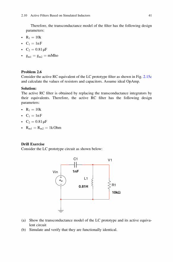
Drill Exercise
Consider the LC prototype circuit as shown below:
R1
Vin
0.81H
V1C1
L1
1nF
10kW
(a) Show the transconductance model of the LC prototype and its active equiva-
lent circuit
(b) Simulate and verify that they are functionally identical.
2.10 Active Filters Based on Simulated Inductors 41
2.11 Higher Order Filters
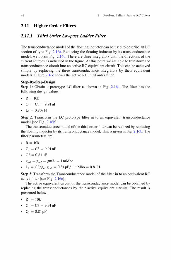
2.11.1 Third Order Lowpass Ladder Filter
The transconductance model of the floating inductor can be used to describe an LC
section of type Fig. 2.16a. Replacing the floating inductor by its transconductance
model, we obtain Fig. 2.16b. There are three integrators with the directions of the
current sources as indicated in the figure. At this point we are able to transform the
transconductance circuit into an active RC equivalent circuit. This can be achieved
simply by replacing the three transconductance integrators by their equivalent
models. Figure 2.16c shows the active RC third order filter.
Step-By-Step-Design
Step 1: Obtain a prototype LC filter as shown in Fig. 2.16a. The filter has the
following design values:
• R ¼ 10k
• C1 ¼ C3 ¼ 9:91nF
• L1 ¼ 0:809H
Step 2: Transform the LC prototype filter in to an equivalent transconductance
model [see Fig. 2.16b]:
The transconductance model of the third order filter can be realized by replacing
the floating inductor by its transconductance model. This is given in Fig. 2.16b. The
filter parameters are:
• R ¼ 10k
• C1 ¼ C3 ¼ 9:91nF
• C2 ¼ 0:81μF• gm1 ¼ gm2 ¼ gm3- ¼ 1mMho
• L1 ¼ C2=gm1gm2 ¼ 0:81μF=1μuMho ¼ 0:81H
Step 3: Transform the Transconductance model of the filter in to an equivalent RC
active filter [see Fig. 2.16c]:
The active equivalent circuit of the transconductance model can be obtained by
replacing the transconductances by their active equivalent circuits. The result is
presented below.
• R1 ¼ 10k
• C1 ¼ C3 ¼ 9:91nF
• C2 ¼ 0:81μF
42 2 Baseband Filters: Active RC Filters

R
Vin
L1
0.80
9H
10kW
C1
ab
c
9.91
0nF
C3
9.91
nF
Vin
0.81
mF
V2 C
2
V1
I1I2
I3
V3=
Vo
10kW
9.91
nF
9.91
nF
10kW
10kW
Vo
9.91
nF0.
809µ
F
1kΩ
V1
10kΩ
1kΩ
9.91
nF
10kΩ
9.91
nF
1kΩ
V3
1kΩ
0.80
9µF
10kΩ
1kΩ
R
R
R
C3
C1
I3=
gm3V
2I2
=gm
2V1-
V3)
I1=
gm1V
2V
1
C3
C1
C1
Rm
1
Rm
1
Rm
2
Rm
2
C2
Rm
3
R
R
R
C2
V2
L =
C2/
(gm
1gm
2)
Vin
Fig.2.16
(a)Athirdorder
LClowpassfilter
(b)thetransconductance
model
and(c)theactiveequivalentcircuitofthethirdorder
lowpassfilter
2.11 Higher Order Filters 43

• Rm1 ¼ 1=gm1 ¼ 1k
• Rm2 ¼ 1=gm2- ¼ 1k
• Rm3 ¼ 1=gm3- ¼ 1k
• L1 ¼ Rm1Rm2C2 ¼ 1k� 1k� 0:81μF ¼ 0:81H
The design is complete.
2.11.2 Fifth Order Lowpass Ladder Filter
The design methods developed in the previous section can be used to construct
higher order ladder filters such as all pole ladder filters. Let’s consider a fifth order
LC prototype as shown in Fig. 2.17a. Replacing the floating inductor by its
transconductance model, we obtain Fig. 2.17b. There are five integrators with the
directions of the current sources as indicated in the figure. The active RC equivalent
circuit can be obtained simply by replacing the corresponding transconductance
integrators by their equivalent models. Figure 2.17c shows the active RC fifth order
ladder filter.
Step-By-Step-Design
Step 1: Obtain a prototype LC filter as shown in Fig. 2.17a. The filter has the
following design values:
• R ¼ 10k
• C1 ¼ C3 ¼ C5 ¼ 9:91nF
• L1 ¼ L2 ¼ 0:81H
Step 2: Transform the LC prototype filter in to an equivalent transconductance
model [see Fig. 2.17b]:
The transconductance model of the fifth order filter can be realized by replacing
the floating inductors by their transconductance models. This is given in Fig. 2.17b.
The filter parameters are:
• R ¼ 10k
• C1 ¼ C3 ¼ C5 ¼ 9:91nF
• C2 ¼ C4 ¼ 0:81μF• gm1 ¼ gm2 ¼ gm3 ¼ gm4 ¼ gm5 ¼ 1mMho
• L1 ¼ C2= gm1gm3ð Þ ¼ 0:81μF=μMho ¼ 0:81H
• L2 ¼ C4= gm3gm5ð Þ ¼ 0:81μF=μMho ¼ 0:81H
Step 3: Transform the Transconductance model of the filter in to an equivalent RC
active filter [see Fig. 2.17c]:
44 2 Baseband Filters: Active RC Filters

10kW
a b c
R
Vin
L1
0.81
H
10kW
C1
9.91
nF
L2
0.81
H
9.91
nF
9.91
nF
v5=
Vo
Vin
0.81
F
V2
C2
I1=
gm1V
2
I1I2
I3
V3
10kW 9.
91n
F9.
91n
F0.
81F
V4 C
4I4
I5
V5
9.91
nF
10kΩ
V1
I2=
gm2(
V1-
V3
I3=
gm3(
V2-
V4)
I4=
gm4(
V3-
V5)
I5=
gm5(
V4)
9.91
nF0.
81µF
1kΩ
V1
10kΩ
1kΩ
10kΩ
9.91
nF
1kΩ
1kΩ
0.81
μF
V2
1kΩ
9.91
nF
1kΩ
V5
10kΩ
9.91
nF1k
Ω
0.81
µF
V3
V4
1kΩ
0.81
μF
1kΩ
9.91
nF
R
C1
C3
C5
C3
C5
V1
V3
RR
Vin
Rm
1
Rm
1
R
R
R
Rm
2
Rm
2
Rm
3
Rm
3
Rm
4
Rm
4
Rm
5
C1
C1
C2
C2
C3
C3
C4
C4
C5
Fig.2.17
(a)Afifthorder
all-pole
LCfilter.(b)Transconductance
model
(c)ActiveRCequivalentcircuit
2.11 Higher Order Filters 45

The active equivalent circuit of the transconductance model can be obtained by
replacing the transconductances by their active equivalent circuits. The result is
presented below.
• R ¼ 10k
• C1 ¼ C3 ¼ C5 ¼ 9:91nF
• C2 ¼ C4 ¼ 0:81μF• Rm1 ¼ Rm2 ¼ Rm3 ¼ Rm4 ¼ Rm5 ¼ 1k
• L1 ¼ Rm1Rm3C2 ¼ 0:81μF=μMho ¼ 0:81H
• L2 ¼ Rm3Rm5C4 ¼ 0:81μF=μMho ¼ 0:81H
The design is complete.
2.12 Conclusions
• Introduces transconductances as filter building blocks
• Grounded and floating inductors are simulated using transconductance models
• Shows how to design active filters from LC prototype filters
• Examples are given to design Higher Order Active Filters Based on Simulated
Inductors
References
1. A.I. Zverev, Handbook of Filter Synthesis (Wiley, New York, 1967)
2. J. Vlach, Computerized Approximation and Synthesis of Networks (Wiley, New York, 1969)
3. G.S. Moschytz, Linear Integrated Networks Design (Van Nostrand Reinhold Company,
New York, 1975)
4. L.T. Bruton, Network Transfer Functions using the concept of FDNR. IEEE Trans. Circuit
Theory CT-16, 406–408 (1969)
5. S.M. Faruque, J. Vlach, T.R. Viswanthan, Switched-capacitor inductors and their use in LC
filter simulation. IEE Proc 128(4), 227–229 (1981)
6. S.M. Faruque, Synthesis of Switched Capacitor Networks and Filters. Ph.D. Thesis, Department
of Electrical Engineering, University of Waterloo, ON, Canada, 1980
7. G. Cramer, Introduction �a l’Analyse des lignes Courbes algebriques (in French). (Europeana,
Geneva, 1750), pp. 656–659. Accessed 18 May 2012
46 2 Baseband Filters: Active RC Filters

Chapter 3
Switched Capacitor Building Blocksand Filters
Topics
• Switched Capacitor Resistor
• Switched Capacitor Integrators
• Switched Capacitor Filter Building Blocks
• Higher order Switched Capacitor Filters
3.1 Switched Capacitor Resistor
In MOS (Metal Oxide Semiconductor) integrated technology, it is relatively simple
to produce transistors and capacitors but resistors present problems. This led a
group of researchers [1, 2] to the idea of replacing resistors by periodically
Switched-Capacitors [1, 2]. Assuming that the clock frequency used to operate
the switches is much higher than the signal frequency a resistor R of value given by
the following equation:
R ¼ 1= fcCr ð3:1Þ
can be generated by means of the arrangement shown in Fig. 3.1b, where
• fc¼Clock frequency
• Cr¼ Switched capacitor
• Φ1 and Φ2 are two complementary non-overlapping clocks (see Fig. 3.1d,
generated by the arrangement as shown in Fig. 3.1c).
The operation of the switched capacitor circuit is as follows:
• In phase 1, S1 is closed (S2 is open). The switched capacitor Cr charges to V1.
The value of the charge is given by:
© Springer International Publishing Switzerland 2015
S. Faruque, Radio Frequency Source Coding Made Easy, SpringerBriefsin Electrical and Computer Engineering, DOI 10.1007/978-3-319-15609-5_3
47
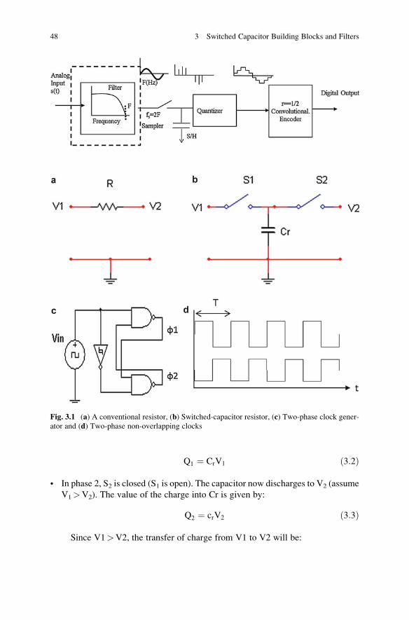
Q1 ¼ CrV1 ð3:2Þ
• In phase 2, S2 is closed (S1 is open). The capacitor now discharges to V2 (assume
V1>V2). The value of the charge into Cr is given by:
Q2 ¼ crV2 ð3:3Þ
Since V1>V2, the transfer of charge from V1 to V2 will be:
Fig. 3.1 (a) A conventional resistor, (b) Switched-capacitor resistor, (c) Two-phase clock gener-
ator and (d) Two-phase non-overlapping clocks
48 3 Switched Capacitor Building Blocks and Filters
ΔQ ¼ Q1 � Q2 ¼ Cr V1 � V2ð Þ ð3:4Þ
If this operation repeats periodically at a rate fc¼ 1/T, where T is the clock
period and fc is the clock frequency, the average current flow from V1 to V2 will be:
I ¼ ΔQ=T ¼ fcCr V1 � V2ð Þ ð3:5Þ
The value of the simulated resistance will be:
R ¼ v1 � V2ð Þ=I ¼ 1= fcCrð Þ ð3:6Þ
Therefore, a capacitor, switching between two nodes, where the nodal voltages are
V1 and V2, simulates a resistor, Which is inversely proportional to the value of
Cr. This is very attractive in IC technology since a large value of resistance can be
realized in a small silicon area. Moreover, the value of the simulated resistor can be
controlled by the clock frequency fc.
3.2 Switched-Capacitor Integratorsand Transconductances
The idea of Switched-Capacitor Transconductance (SCT) was developed earlier
[3, 4]. In this section we consider a similar approach to develop transconductance
models of various SC-Integrators.
Let us consider the conventional RC-Integrator as shown in Fig. 3.2a. Replacing
the resistor by a switched-capacitor resistor, we obtain the SC-Integrator as shown
in Fig. 3.2b. Two-phase clock is assumed with the left switch S1 closed in phase
1 and the right switch S2 closed in phase 2.
During phase-1, the capacitor Cr is charged to the voltage Vin. During phase 2, it
is connected at the negative input of the operational amplifier which is at the virtual
ground. Now the capacitor sees a zero potential between its terminals and it is
discharged instantaneously.
The amount of charge which is transferred into the feedback capacitor C will be
ΔQ¼CrVin. It is assumed that the operational amplifier is ideal.
If this operation is repeated at a clock rate T, the average value of current flowing
through the capacitor C will be given by
I ¼ ΔQ=T ¼ CrVin=T ¼ fcCrVin ¼ gmVin ð3:7Þ
where
3.2 Switched-Capacitor Integrators and Transconductances 49
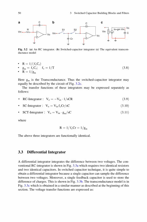
• R ¼ 1= fcCrð Þ• gm ¼ fcCr; fc ¼ 1=T• R ¼ 1=gm
ð3:8Þ
Here gm is the Transconductance. Thus the switched-capacitor integrator may
equally be described by the circuit of Fig. 3.2c.
The transfer functions of these integrators may be expressed separately as
follows:
• RC-Integrator : Vo ¼ �Vin � 1=sCR ð3:9Þ• SC-Integrator : Vo ¼ Vin fcCr=sC ð3:10Þ• SCT-Integrator : Vo ¼ Vin � gm=sC ð3:11Þ
where
R ¼ 1= fcCr ¼ 1=gm
The above three integrators are functionally identical.
3.3 Differential Integrator
A differential integrator integrates the difference between two voltages. The con-
ventional RC-integrator is shown in Fig. 3.3a which requires two identical resistors
and two identical capacitors. In switched capacitor technique, it is quite simple to
obtain a differential integrator because a single capacitor can sample the difference
between two voltages. Moreover, a single feedback capacitor is used to store the
difference of charges. This is shown in Fig. 3.3b. The transconductance model is in
Fig. 3.3c which is obtained in a similar manner as described at the beginning of this
section. The voltage transfer functions are expressed as:
R
C C
VinVinVo Vo
S1 S2
Cr
Vin
Vo
C
Io=gm Vin
a b c
Fig. 3.2 (a) An RC integrator. (b) Switched-capacitor integrator (c) The equivalent transcon-
ductance model
50 3 Switched Capacitor Building Blocks and Filters

• RC-Integrator : Vo ¼ � V1 � V2ð Þ1=sCR ð3:12Þ• SC-Integrator : Vo ¼ � V1 � V2ð Þ fcCr=sC ð3:13Þ• SCT-Integrator : Vo ¼ � V1 � V2ð Þgm=sC ð3:14Þ
Once again, the three integrators are functionally identical.
Other realization of integrators such as non-inverting summing, multi-input etc.
will follow an obvious pattern. An example of a non-inverting integrator with
V1¼ 0, is given in Fig. 3.3d and its SC counterpart in Fig. 3.3e.
3.4 Z-Domain Analysis
3.4.1 Switched Capacitor (Sc) Resistor
A switched-capacitor network is essentially a sampled-data network. Therefore for
an accurate result, z-domain analysis is required. The resemblance between a
sampled-data network and its continuous time counterpart depends primarily on
the type of transformation which describes the sampled-data system. One such
transformation is the LDI-Transformation (Loss-less Digital Integrator) [5]. In
order to examine the behavior of a capacitor in the switching mode, let us consider
the switched-capacitor resistor simulation circuit once again. This is shown in
Fig. 3.4 along with the switching scheme.
R
C C
V1Vo Vo
Cr
V1Vo
C
Io = gm(V1-V2)
V2R C
a b c
d e
V1
V2V2
R
CC
V1=0Vo Vo
S1 S2
S1 S2
S1 S2
CrV2
RC
V2S1 S2
V1=0
Fig. 3.3 (a) An RC-differential integrator. (b) Switched capacitor differential integrator. (c) Thetransconductance model (d) Non-inverting integrator, (e) SC non-inverting integrator
3.4 Z-Domain Analysis 51

During phase 1, Cr samples the Voltage V1(nT). During phase 2, it is discharged
to the voltage V2(n +½)T. The amount of charge flowing from port 1 to port 2 is
given by:
q1,2 nTð Þ ¼ CrV2 nþ ½ð ÞT� CrV1 nTð Þ ð3:15Þ
If we start from the second port of Fig. 3.4, we obtain by similar reasoning
q2,1 nTð Þ ¼ CrV1 nþ ½ð ÞT� CrV2 nTð Þ ð3:16Þ
The above equations can be expressed in terms of delays as well:
q1,2 nTð Þ ¼ CrV2 nTð Þ � CrV1 n� ½ð ÞT ð3:17Þq2,1 nTð Þ ¼ CrV1 nTð Þ � CrV2 n� ½ð ÞT ð3:18Þ
In the z-domain, the above equations are expressed as:
Q1,2 zð Þ ¼ CrV2 zð Þ � CrV1 zð ÞZ�½ ð3:19Þ
Q2,1 zð Þ ¼ CrV1 zð Þ � CrV2 zð ÞZ�½ ð3:20Þ
In the above Z-domain equations, Z�½ represents a half delay.
3.4.2 Switched Capacitor (sC) Integrator
Let us now introduce an ideal operational amplifier in conjunction with the
switched-capacitor as shown in Fig. 3.5.
Operation of the SC-Integrator is as follows:
During phase-1, the capacitor Cr is charged to the voltage Vin. The amount of
charge sampled at the sampling instant nT will be:
Fig. 3.4 A switched-capacitor resistor and its timing diagram
52 3 Switched Capacitor Building Blocks and Filters
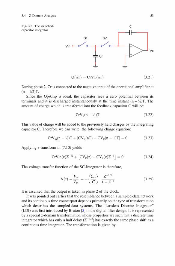
Q nTð Þ ¼ CrVin nTð Þ ð3:21Þ
During phase 2, Cr is connected to the negative input of the operational amplifier at
(n� 1/2)T.
Since the OpAmp is ideal, the capacitor sees a zero potential between its
terminals and it is discharged instantaneously at the time instant (n�½)T. The
amount of charge which is transferred into the feedback capacitor C will be:
CrV1 n�½ð ÞT ð3:22Þ
This value of charge will be added to the previously held charges by the integrating
capacitor C. Therefore we can write: the following charge equation:
CrVin n� ½ð ÞTþ CV0 nTð Þ � CV0 n� 1ð ÞT½ � ¼ 0 ð3:23Þ
Applying z-transform in (7.10) yields
CrVin zð ÞZ�½ þ CV0 zð Þ � CV0 zð ÞZ�1� � ¼ 0 ð3:24Þ
The voltage transfer function of the SC-Integrator is therefore,
H zð Þ ¼ Vo
Vin¼ � Cro
C
� �Z�1=2
1� Z�1ð3:25Þ
It is assumed that the output is taken in phase 2 of the clock.
It was pointed out earlier that the resemblance between a sampled-data network
and its continuous time counterpart depends primarily on the type of transformation
which describes the sampled-data systems. The “Lossless Discrete Integrator”
(LDI) was first introduced by Bruton [5] in the digital filter design. It is represented
by a special z-domain transformation whose properties are such that a discrete time
integrator which has only a half delay (Z�1/2) has exactly the same phase shift as a
continuous time integrator. The transformation is given by
Fig. 3.5 The switched-
capacitor integrator
3.4 Z-Domain Analysis 53
S ¼ 1
T
1� Z�1
Z�1=2ð3:26Þ
Substituting for Z¼ ejωT, we obtain
S ¼ j2
TSin ωT=2ð Þ ð3:27Þ
which is purely imaginary? Thus the discrete time integrator has the same phase
shift as an analog integrator. The discrete time voltage transfer function can be
expressed as:
H zð Þ ¼ H sð Þ ¼ � Cr=Cð Þ1=ST¼ � fcCr=sC¼ �gm=sC
ð3:28Þ
Thus the transconductance concept which was developed in the previous section is
valid through the LDI transformation.
3.4.3 Frequency Response of SC-Integrator
In order to evaluate the frequency response of the SC-Integrator, consider the
z-domain transfer function as s given below:
H zð Þ ¼ V0=Vin ¼ �Cr
C
Z�½
1� Z�1ð3:29Þ
Substitute for Z¼ ejωT to obtain
H e jωT� � ¼ � Cm=Cð Þ ωTð Þ2 jωT Sin ωT=2ð Þ½ � ð3:30Þ
This transfer function should be compared with the conventional analog integrator
which has a transfer function
H jωð Þ ¼ � 1
jωRCð3:31Þ
They both are purely imaginary. The amplitude response Is similar as well if ω is
chosen so small that Sin(ωT/2) ~ωT/2.
54 3 Switched Capacitor Building Blocks and Filters

3.5 Switched-Capacitor Biquad Filters
A biquad (bi-quadratic) filter is a second order filter which can provide various
second order transfer functions. A biquad transfer function is the one whose
numerator and denominator polynomials are quadratic in nature. Chapter 2 pro-
vides some of the most useful second order transfer functions and their frequency
responses. In this section we will briefly review lowpass and bandpass functions
and realize them by means of switched capacitor technique.
3.5.1 Lowpass Filter
A Lowpass filter is described by the following transfer function:
T sð Þ ωz
s2 þ ω pQ p
� sþ ω p
ð3:32Þ
where,
s¼ jω Laplace transform variable
ωz¼ zeroes of the transfer function
ωp¼ poles of the transfer function
Qp¼ quality factor of the poles
Zeros are described by the numerator polynomial and Poles are described by the
denominator polynomial. Most frequently used transfer functions are described in
the following:
The frequency response is shown in Fig. 3.6. The pole frequency ωp is measured
when the voltage transfer function |T(s) is 70 % of its maximum value.
Fig. 3.6 A lowpass
response. ωp is the pole
frequency
3.5 Switched-Capacitor Biquad Filters 55

3.5.2 Bandpass Filter
A band pass filter is described by its transfer function
T sð Þ ¼ωzQz
� s
s2 þ ω pQ p
� sþ ω p
ð3:33Þ
It has a frequency response as shown in Fig. 3.7, where ωp is the pole frequency.
3.5.3 Switched Capacitor Biquad
Let us consider the RC active Biquad filter as shown in Fig. 3.8a. This circuit has
two voltage transfer functions as follows:
• H1(s)¼V1/Vin and
• H2(s)¼V2/Vin.
For the above voltage transfer functions, we need to find solutions for V1 and
V2. Since there are two equations and two unknowns V1 and V2, we will use
Cramer’s rule to find the solution for V1 and V2 [6]. We will also use resistors as
conductors G (G¼ 1/R) and capacitors as frequency dependent conductance sC
(impedance¼ 1/sC) where s¼ jω. It is assumed that the students are familiar with
Cramer’s rule. Briefly, Cramer’s rule is an explicit formula for the solution of a
system of linear equations. It finds the solution in terms of determinants of matrices.
Fig. 3.7 Bandpass
response
56 3 Switched Capacitor Building Blocks and Filters

Now, consider the second order Biquad filter as shown in Fig. 3.8a. Here, we need
to find the solution for V1 and V2. We will use nodal equations, which is essentially
KCL. There are two nodal equations: one at the negative input of the first OpAmp
(Node 1) and the other at the negative input of the second OpAmp (Node 2). Note
that there are no nodal equations at vin, V1 and V2, since there ideal voltage sources.
At node 1, the nodal equation is given by:
V2 G1 þ sC1ð Þ � V1sC1 � VinG1 ¼ 0
At node 2, the nodal equation is:
0 G2 þ sC2ð Þ � V1G2 � V2sC2 ¼ 0
Notice that the first term is stricken out since it is multiplied by zero. This is due to
the fact that this node is virtual ground.
The above equations can be written as a 2� 2 matrix:
�sC1 G1þ sC1�G2 �sC2
�V1V2
�¼ VinG1
0
�
Node 1a
b
Node 2
Vin
VinVin
R1R2
C1C2
S1 S2S1 S2
V1
V1
−
+−
−+
+−
+
−
+
−
+
V2
V2
Fig. 3.8 Second order filter. (a) A second order b-quadratic (biquad) filter. (b) Switched capacitorbiquad
3.5 Switched-Capacitor Biquad Filters 57

In order to find the solution for V1 and V2, we will use Cramer’s rule. The process
is as follows:
Step 1: Find the determinant D as:
D ¼ �sC1 G1þ sC1�G2 �sC2
�¼ s2C1C2 þ sC1G2 þ G1G2
where,
• D is the denominator of the second order polynomial.
• It determines ωo and Q
Step 2: Replace the first column of the matrix by the right hand side of the equation
and find the determinant D1.
D1 ¼ VinG1 G1þ sC10 �sC2
�¼ �VinSC2G1
where,
• D1 finds the solution for V1 and determines the numerator polynomial for the
first transfer function H1(s).
• It also determines the type of the filter
Step 3: Replace the second column of the matrix by the right hand side of the
equation and find the determinant D2.
D2 ¼ �sC1 VinG1�G2 0
�¼VinG1G2
where,
• D2 finds the solution for V2 and determines the numerator polynomial for the
second transfer function H2(s).
• It also determines the type of the filter
Step 4 : Find the Solutions for V1 and V2:
V1 ¼ D1
D¼ �VinsC2G1
D
V2 ¼ D2
D¼ VinG1G2
D
58 3 Switched Capacitor Building Blocks and Filters

Step 5: Find the voltage transfer functions:
H1 sð Þ ¼ V1
Vin¼ �sC2G1
D
H2 ¼ V2
Vin¼ VinG1G2
D
where,
D ¼ s2C1C2 þ sC1G2 þ G1G2
Therefore,
• H1(s) is a bandpass function and
• H2(s) is a lowpass function
Notice that D is a quadratic function, common to both transfer functions. It is the
numerator which determines the type of filter. In this case, H1(s) is a second order
bandpass filter and H2(s) is a second order lowpass filter.
Comparing the denominator with the characteristics equation, we can write:
S2 þ s ωo=Qð Þ þ ω2o ¼ s2C1C2 þ s= C2R2ð Þ þ 1= R1R2C1C2ð Þ
where,
ω0 ¼ffiffiffiffiffiffiffiffiffiffiffiffiffiffiffiffiffiffiffiffiffiffiffi
1
R1R2C1C2
r
Q ¼ffiffiffiffiffiffiffiffiffiffiffiffiR2C2
R1C1
r
The equivalent switched capacitor filter is obtained simply by replacing the resis-
tors by their sC circuit. This is shown in Fig. 3.8b. The values of the sc resistors are:
• R1¼ 1/(fcCr1)
• R2¼ 1/(fcCr2)
• fc¼Clock frequency.
3.6 Switched-Capacitor Filters Based on SimulatedInductors
In this section we shall consider the design of switched-capacitor filters based on
simulated inductors. The step-by-step design process is as follows:
• Obtain an LC prototype filter
• Model the LC prototype filter by means of transconductances
3.6 Switched-Capacitor Filters Based on Simulated Inductors 59

• Design the active RC equivalent circuit by means of OpAmps, resistors and
capacitors.
• Replace RC active integrators by means of SC equivalent integrators.
In order to simplify the design we shall consider identical examples and will
refer to Chap. 2 whenever it is necessary.
3.6.1 SC Realization of Second Order LC Filters
Let us consider the second order active RC filter as shown in Fig. 3.9a. This is the
same circuit which was designed from a second order passive LC prototype (see
Chap. 2). The SC equivalent circuit is obtained by replacing the active RC integra-
tors by means of their SC equivalent circuits. This is shown in Fig. 3.9b. Here, SC
resistors are simulated as follows:
C1
S1 S2
Cr1
Vin
C2
V2Cr2
V1
Cr3
S1 S2
S1 S2
S1 S2
V11 Vpk1000 Hz 0
1nF0.81μF
1kΩ V2V1
10kΩ
1kΩ 1nF
10kΩ
1kΩ
a
b S1 S2
Cr1
−
+
−
+
−
+−+
−
+−+
Fig. 3.9 (a) A second order active RC filter and (b) SC-equivalent circuit
60 3 Switched Capacitor Building Blocks and Filters

• The first stage has a non-inverting integrator and an inverting amplifier. The
non-inverting integrator has a pair of 1k resistors. This stage is realized by means
of a differential switched capacitor scheme as shown in the figure. The amplifier
stage has a pair of 10k resistors. This stage is realized separately by means of two
SC resistors.
• The second stage is an inverting integrator. This stage is realized by means of an
inverting SC integrator.
The values of the resistors are given by:
For the first state:
• 10k¼ 1/fcCr1
• 1k¼ 1/FcCr3
For the second stage:
• 1 k¼ 1/fcCr2
The clock frequency fc is the same for both the stages.
3.6.2 SC Realization of Third Order LC Ladder Filters
Let us consider the third order active RC filter as shown in Fig. 3.10a. This is the
same circuit which was designed from a third order passive LC prototype filter (see
Chap. 2).
The SC equivalent circuit is obtained by replacing the active RC integrators by
means of their SC equivalent circuits. This is shown in Fig. 3.10b. Here, SC
resistors are simulated as follows:
• The first stage has a non-inverting integrator and an inverting amplifier. The
non-inverting integrator has a pair of 1k resistors. This stage is realized by means
of a differential switched capacitor scheme as shown in the figure. The amplifier
stage has a pair of 10k resistors. This stage is realized separately by means of two
SC resistors.
• The second stage is a differential integrator. This stage is realized by means of a
differential SC-integrator.
• The third stage is an inverting integrator. This stage is realized by means of an
inverting SC integrator.
The values of the resistors are given by:
For the first stage:
• 10 k¼ 1/fcCr1
• 1 k¼ 1/fcCr11
For the second stage:
• 1 k¼ 1/fcCr2
3.6 Switched-Capacitor Filters Based on Simulated Inductors 61

For the third stage:
• 1 k¼ 1/fcCr3
The clock frequency fc is same for all the stages.
Problem
Consider the fifth order ladder filter as shown below:
(a) Find the frequency response by means of simulation (Use Multisim or PSpice).
(b) Design the equivalent fifth order SC ladder Filter
(c) Calculate the values of SC resistors for fc¼ 20 kHz.
1 Vpk1000 Hz0°
9.91nF0.81μF
1kΩV1
10kΩ
1kΩ9.91nF
10kΩ 9.91nF
1kΩ V31kΩ
0.81μF
10kΩ
V2
1kΩ
Vin
a
b
Cr1Vin
C2
V2V1
Cr11
C3
V3Cr3
Cr2
C1S1 S2
S1 S2
S1 S2 S1 S2
S1 S2
S1 S2
S1 S2
Cr1
-
+-
+
+-
-
+
-
+-
+
-
+
+-
Fig. 3.10 (a) A third order active RC filter and (b) SC-equivalent circuit
62 3 Switched Capacitor Building Blocks and Filters
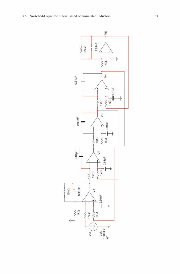
Vin
1 V
pk10
00 H
z0°
9.91
nF0.
81μF
1k Ω
1k Ω
1k Ω
1k Ω
1k Ω
1k Ω
10k
Ω
V1
10k
Ω
1k Ω
10k
Ω
9.91
nF
1k Ω
0.81
μF
V2
1k Ω
9.91
nF
V5
9.91
nF
0.81
μF
V3
V4
0.81
μF
9.91
nF
3.6 Switched-Capacitor Filters Based on Simulated Inductors 63

3.7 Conclusions
• Described the realization of Switched Capacitor Resistor and its use in IC
technology
• Presented switched capacitor integrators and various switched capacitor build-
ing blocks for filter design
• Examples are given to illustrate the concept
References
1. J.T. Caves, J.M.A. Copeland, C.F. Rahim, S.D. Rosenbaum, Sampled analog filtering using
switched-capacitors as resistors. IEEE J. Solid State Circuits SC-12, 592–599 (1977)
2. B.J. Hosticka, R.W. Brodersen, P.R. Gray, MOS sampled data recursive filters using switched-
capacitors as resistor. IEEE J. Solid State Circuits 12, 600–608 (1977)
3. T.R. Viswanathan, S.M. Faruque, K. Signghal, J. Vlach, Switched-capacitor transconductance
and related building blocks. IEEE Trans. Circuits Syst. 27(6), 502–508 (1980)
4. S.M. Faruque, Synthesis of Switched Capacitor Networks and Filters. Ph.D. Thesis, Department
of Electrical Engineering, University of Waterloo, ON, Canada, 1980
5. L.T. Bruton, Low sensitivity digital ladder filters. IEEE Trans. Circuits Syst. 22, 168–176(1975)
6. G. Cramer, Introduction �a l’Analyse des lignes Courbes algebriques (in French). (Europeana,
Geneva, 1750), pp. 656–659. Accessed 18 May 2012
64 3 Switched Capacitor Building Blocks and Filters

Chapter 4
Pulse Code Modulation (PCM)
Topics
• Introduction to PCM
• Sampling
• Quantization-Linear and Non-Linear
• A/D and D/A Converter
• Bit Rate and Bandwidth
4.1 Introduction to PCM
Pulse Code Modulation (PCM), also known as baseband transmission, converts the
input analog signal into digital format and transmits over a digital communication
channel. Figure 4.1 shows the basic functional block diagram of a typical PCM
system. It Involves:
• Band limiting the input analog signal (See Chaps. 2 and 3)
• Sampling
• Quantization
• A to D conversion
• Signal shaping
Several PCM channels can be multiplexed to forms a single bit stream and
transmit over a single digital channel. This is known as time Division Multiplexing
(TDM). For example, the classical land telephone system is a TDM system where
24 digital channels are multiplexed to form a single digital channel. Similar
multiplexing techniques are also used in modern cellular communication systems.
We will discuss this further in this book. This chapter brings readers up-to-date in
key concepts and underlying principles of PCM so that they can readily apply it to
the industry.
© Springer International Publishing Switzerland 2015
S. Faruque, Radio Frequency Source Coding Made Easy, SpringerBriefsin Electrical and Computer Engineering, DOI 10.1007/978-3-319-15609-5_4
65

4.2 Input Band-Limit Filter
This topic has already been detailed in the preceding chapter. This brief summary is
included so that readers may connect it to the topic which follows. As shown in
Fig. 4.2, the input analog signal may contain undesired signals along with the
desired signal. The transmission bandwidth is also limited. Therefore, we need a
lowpass filter to remove the undesired signals. These filters are known as band-limit
filters. The output of the lowpass filter is the desired signal, which is band limited
for further processing.
Once the desired analog signal is recovered, the next step of the process is
sampling. The maximum frequency available for sampling is fm, which is the output
of the band limit filter as shown in the figure. These band limit filters, also known as
antialiasing filters, play an important role in sampling, as we shall see in the
following section.
Fig. 4.1 PCM functional block diagram
Fig. 4.2 Band-limit filter rejects unwanted signals by means of a lowpass filter and keeps the
desired signal. The maximum frequency available for sampling is fn
66 4 Pulse Code Modulation (PCM)

4.3 Sampling [1, 2]
In PCM, sampling is the conversion of continuous signal to a sequence of a discrete
time signal as shown in Fig. 4.3.
In Fig. 4.3:
• m(t) is the input signal
• S(t) is the sampled output signal, before and after Sample & Hold (S/H)
• fs¼ 1/Ts is the sampling frequency
• Ts¼ 1/fs is the sample period.
According to Nyquist sampling theorem [1]:
• Nyquist Rate is defined as: fs¼2fm• Nyquist Criterion is defined as: fs� 2fm
The sampling frequency or sampling rate, fs, is the average number of samples
obtained in 1 s (samples per second). In this mechanism, the analog signal ampli-
tude is sampled (measured) at regular time intervals. The sampling rate, or number
of samples per second, is several times the maximum frequency of the analog
waveform in cycles per second. The following problem will show how sampling
frequency governs the reconstruction of the analog signal.
Problem 4.1
Given:
• Analog signal frequency fm¼ 1 kHz
Show the sampled analog signal S(t) for the following sampling frequencies:
• fs¼ 8 kHz
Fig. 4.3 Illustration of sampling. According to Nyquist criterion, the sampling frequency should
be greater than twice the input signal frequency to reconstruct the input signal m (t). S(t) is the
sampled signal before and after sample and hold (S/H)
4.3 Sampling 67
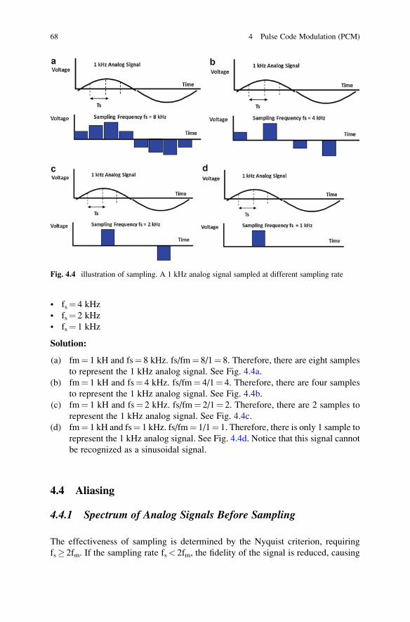
• fs¼ 4 kHz
• fs¼ 2 kHz
• fs¼ 1 kHz
Solution:
(a) fm¼ 1 kH and fs¼ 8 kHz. fs/fm¼ 8/1¼ 8. Therefore, there are eight samples
to represent the 1 kHz analog signal. See Fig. 4.4a.
(b) fm¼ 1 kH and fs¼ 4 kHz. fs/fm¼ 4/1¼ 4. Therefore, there are four samples
to represent the 1 kHz analog signal. See Fig. 4.4b.
(c) fm¼ 1 kH and fs¼ 2 kHz. fs/fm¼ 2/1¼ 2. Therefore, there are 2 samples to
represent the 1 kHz analog signal. See Fig. 4.4c.
(d) fm¼ 1 kH and fs¼ 1 kHz. fs/fm¼ 1/1¼ 1. Therefore, there is only 1 sample to
represent the 1 kHz analog signal. See Fig. 4.4d. Notice that this signal cannot
be recognized as a sinusoidal signal.
4.4 Aliasing
4.4.1 Spectrum of Analog Signals Before Sampling
The effectiveness of sampling is determined by the Nyquist criterion, requiring
fs� 2fm. If the sampling rate fs< 2fm, the fidelity of the signal is reduced, causing
Fig. 4.4 illustration of sampling. A 1 kHz analog signal sampled at different sampling rate
68 4 Pulse Code Modulation (PCM)
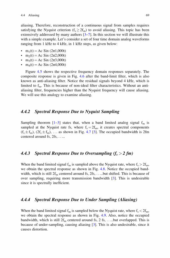
aliasing. Therefore, reconstruction of a continuous signal from samples requires
satisfying the Nyquist criterion (fs� 2fm) to avoid aliasing. This topic has been
extensively addressed by many authors [3–7]. In this section we will illustrate this
with a simple example. Let’s consider a set of four time domain analog waveforms
ranging from 1 kHz to 4 kHz, in 1 kHz steps, as given below:
• m1(t)¼Ac Sin (2π1,000t)• m2(t)¼Ac Sin (2π2,000t)• m3(t)¼Ac Sin (2π3,000t)• m4(t)¼Ac Sin (2π4,000t)
Figure 4.5 shows the respective frequency domain responses separately. The
composite response is given in Fig. 4.6 after the band-limit filter, which is also
known as anti-aliasing filter. Notice the residual signals beyond 4 kHz, which is
limited to fm. This is because of non-ideal filter characteristics. Without an anti-
aliasing filter, frequencies higher than the Nyquist frequency will cause aliasing.
We will use this analogy to examine aliasing.
4.4.2 Spectral Response Due to Nyquist Sampling
Sampling theorem [1–3] states that, when a band limited analog signal fm is
sampled at the Nyquist rate fs, where fs¼ 2fm, it creates spectral components
(fs� fm), (2fs� fm), . . . as shown in Fig. 4.7 [3]. The occupied bandwidth is 2fm
centered around fs, 2fs, . . ...
4.4.3 Spectral Response Due to Oversampling (fs> 2 fm)
When the band limited signal fm is sampled above the Nyquist rate, where fs> 2fm,
we obtain the spectral response as shown in Fig. 4.8. Notice the occupied band-
width, which is still 2fm centered around fs, 2fs, . . ...but shifted. This is because ofover sampling, requiring more transmission bandwidth [3]. This is undesirable
since it is spectrally inefficient.
4.4.4 Spectral Response Due to Under Sampling (Aliasing)
When the band limited signal fm is sampled below the Nyquist rate, where fs< 2fm,
we obtain the spectral response as shown in Fig. 4.9. Also, notice the occupied
bandwidth, which is still 2fm centered around fs, 2 fs, . . ...but overlapped. This isbecause of under-sampling, causing aliasing [3]. This is also undesirable, since it
causes distortion.
4.4 Aliasing 69
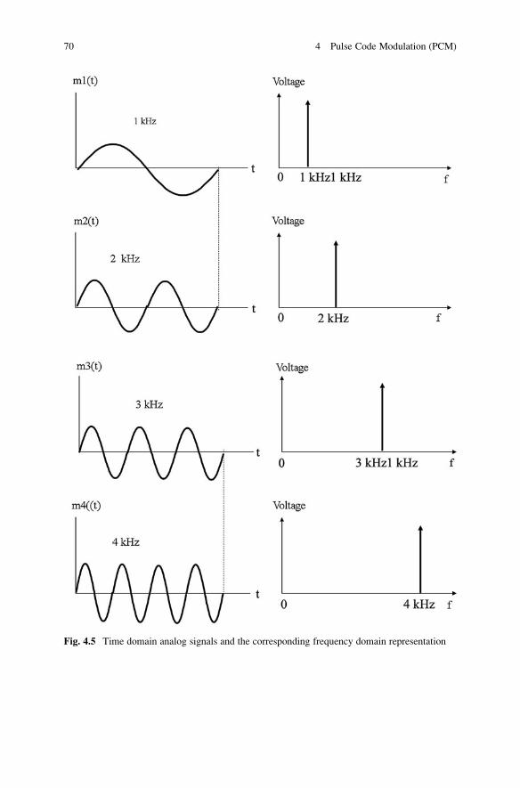
Fig. 4.5 Time domain analog signals and the corresponding frequency domain representation
70 4 Pulse Code Modulation (PCM)
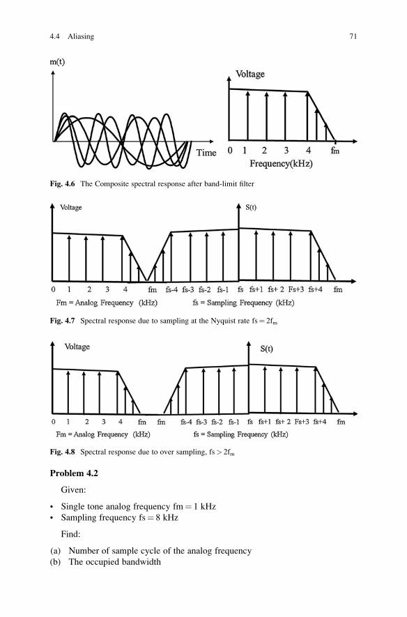
Problem 4.2
Given:
• Single tone analog frequency fm¼ 1 kHz
• Sampling frequency fs¼ 8 kHz
Find:
(a) Number of sample cycle of the analog frequency
(b) The occupied bandwidth
Fig. 4.6 The Composite spectral response after band-limit filter
Fig. 4.7 Spectral response due to sampling at the Nyquist rate fs¼ 2fm
Fig. 4.8 Spectral response due to over sampling, fs> 2fm
4.4 Aliasing 71
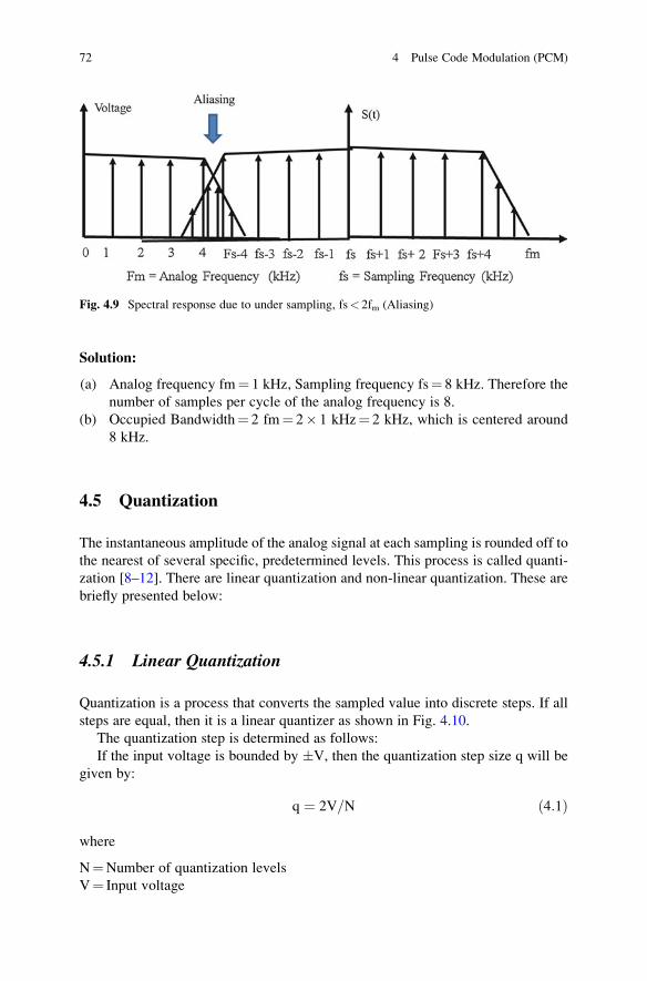
Solution:
(a) Analog frequency fm¼ 1 kHz, Sampling frequency fs¼ 8 kHz. Therefore the
number of samples per cycle of the analog frequency is 8.
(b) Occupied Bandwidth¼ 2 fm¼ 2� 1 kHz¼ 2 kHz, which is centered around
8 kHz.
4.5 Quantization
The instantaneous amplitude of the analog signal at each sampling is rounded off to
the nearest of several specific, predetermined levels. This process is called quanti-
zation [8–12]. There are linear quantization and non-linear quantization. These are
briefly presented below:
4.5.1 Linear Quantization
Quantization is a process that converts the sampled value into discrete steps. If all
steps are equal, then it is a linear quantizer as shown in Fig. 4.10.
The quantization step is determined as follows:
If the input voltage is bounded by �V, then the quantization step size q will be
given by:
q ¼ 2V=N ð4:1Þ
where
N¼Number of quantization levels
V¼ Input voltage
Fig. 4.9 Spectral response due to under sampling, fs< 2fm (Aliasing)
72 4 Pulse Code Modulation (PCM)

Therefore, the number of binary digits that can be represented, will be given by
the following equation:
N ¼ 2n ð4:2Þ
Where
n ¼ Number of binary digits 1; 2; . . .ð Þ
4.5.2 Drawback of Linear Quantization
In Fig. 4.10, If the input voltage is between 0.5 and 1 V, then Output¼ 1 V. This is
to say that:
• y¼ 0 V if 0 V< x< 0.5 V
• y¼ 1 V if 0.5 V< x< 1 V
All samples will fall into a particular quantization interval. This will cause
Quantization error, depending on the interval. Quantization error is high when the
input voltage is low. Quantization error is low when the input voltage is high. Let’s
examine these by means of the following examples:
Example 1
• x¼ 0.1 to 0.2
• Step Size¼ 0.1 V
• y¼ 0.2 (two steps)
• Error¼ 0.1/0.2¼ 0.5 (50 %)
Example 2
• x¼ 0.9 to 1
• Step Size 0.1 V
• y¼ 1
• Error¼ 0.1/1¼ 0.1 (10 %)
Therefore the error is non-Uniform, which is not good.
Fig. 4.10 Illustration of
linear quantization
4.5 Quantization 73

4.6 Non-linear Quantization
A non-linear quantizer, shown in Fig. 4.11, uses:
• Small steps for low input voltages and
• Large steps for large input voltages
Example 1
• x¼ 0.1 to 0.11
• Step Size 0.01 V
• y¼ 0.2
• Error¼ 0.01/0.2¼ 0.05 (5 %)
Example 2
• x¼ 0.95 to 1
• Step Size 0.05 V
• y¼ 1
• Error¼ 0.05/1¼ 0.05 (5 %)
Thus, the quantization error is the same in both cases, which is good.
4.7 Companding
Companding is a process of compression and expansion of signals amplitudes. In
telecommunications, the signal to be transmitted is compressed before transmission
and expanded at the receiver to recover the original signal [13–16]. See Fig. 4.12.
Companding allows signals with a large dynamic range over a channel having
small dynamic range capabilities. Non-uniform quantization can be achieved by
first compressing the samples of the input signal and then expanding at the receiver.
One such method commonly used in PCM is called “Logarithmic Companding”. It
is also known as μ-Law, which is given by the following formula [8]:
Fig. 4.11 Illustration of
non-linear quantization
74 4 Pulse Code Modulation (PCM)

F xð Þ ¼ ln 1þ μxð Þln 1þ μð Þ ð4:3Þ
Where
• F(x)¼Output quantized level
• x¼ Input voltage steps
• μ¼ 0 to 255(Quantization levels)
For μ¼ 0, it is linear (no companding) and for μ> 0, it is non-linear. Figure 4.13
shows the output quantized level F(xxxx) as a function of input voltage steps x for
several values of μ.
Fig. 4.12 Illustration of (a) Logarithmic compression and (b) logarithmic expansion
1
0.9
0.8
0.7
0.6
0.5F(x
)
Normalized X
0.4
0.3
0.2
0.1
00 0.2 0.4 0.6
u=10
u=100
u=256
0.8 1
Fig. 4.13 Illustration of logarithmic companding known as μ-law
4.7 Companding 75

4.8 Digital to Analog Converter
A digital to analog converter (A/D) converter is essentially a summing amplifier
where the voltage gains are binary weighted [9]. In order to understand this, let’s
consider the inverting amplifier as shown in Fig. 4.14. The output voltage of this
amplifier is given by,
Vo
10k
Vref
b0
b1
b2
10k
5k
2.5k
−1V
V0 ¼ �V1 R2=R1ð Þ ¼ AvV1 ð4:4Þ
Where,
Av¼R2/R1 is the voltage gain.
Next, consider the summing amplifier as shown in Fig. 4.15. The output voltage
of this amplifier is given by,
V0 ¼ �Vref
��R2=R1ð Þ þ 2 R2=R1ð Þ þ 4 R2=R1ð Þ þ 8 R2=R1ð Þ
¼ �VrefAv 1þ 2þ 4þ 8½ � ð4:5Þ
For a given reference voltage Vref and R2/R1 ratio, the output voltage Vo is binary
weighted. Therefore, we can select a set of binary numbers to generate a desired
analog output voltage. The desired binary number can be selected by controlling the
binary weighted resistors as shown in Fig. 4.16, which is a 4-bit D/a converter.
Vo
R1
R2
V1
Fig. 4.14 Inverting
amplifier
76 4 Pulse Code Modulation (PCM)
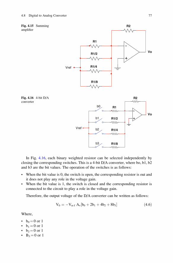
In Fig. 4.16, each binary weighted resistor can be selected independently by
closing the corresponding switches. This is a 4-bit D/A converter, where bo, b1, b2
and b3 are the bit values. The operation of the switches is as follows:
• When the bit value is 0, the switch is open, the corresponding resistor is out and
it does not play any role in the voltage gain.
• When the bit value is 1, the switch is closed and the corresponding resistor is
connected to the circuit to play a role in the voltage gain.
Therefore, the output voltage of the D/A converter can be written as follows:
V0 ¼ �Vre f Av b0 þ 2b1 þ 4b2 þ 8b3½ � ð4:6Þ
Where,
• b0¼ 0 or 1
• b1¼ 0 or 1
• b2¼ 0 or 1
• B3¼ 0 or 1
Vo
R1
R2
Vref
R1/2
R1/4
R1/8
b0
b1
b2
b3
Fig. 4.16 4-bit D/A
converter
Vo
R1
R2
R1/2
R1/4
R1/8
Vref
Fig. 4.15 Summing
amplifier
4.8 Digital to Analog Converter 77

Problem 4.3
Given:
• Vref¼�1 V
• Av¼ 1
(a) Design a 3-bit D/A converter.
(b) Calculate the analog voltage and the corresponding digital input.
Solution:
(a) With Vref �1 V and Av¼ 1, the 3-bit D/A converter appears as follows:
(b) The output voltage for a 3-bit D/A converter is given by,
V0 ¼ �Vref R2=R1ð Þ b0 þ 2b1 þ 4b2½ � Volts¼ b0 þ 2b1 þ 2b2½ � Volts
Table 4.1 shows the analog output corresponding to input digital data.
4.9 Analog to Digital Converter
Analog to digital Converter (ADC) converts the quantized voltage into a bit pattern,
typically 8-bit A/D converter. Figure 4.17 shows the basic block diagram of an n-bit
analog to digital (A/D) converter [9]. It comprises:
• A voltage comparator
• An up-down counter and
• A D to A converter
The operation of the circuit is briefly presented below:
Table 4.1 Output voltage as
a function of input datab2 b1 b0 V0¼ [b0 + 2b1 + 4b2] volts
0 0 0 0
0 0 1 1
0 1 0 2
0 1 1 3
1 0 0 4
1 0 1 5
1 1 0 6
1 1 1 7
78 4 Pulse Code Modulation (PCM)

4.9.1 Function of the Comparator
The analog comparator compares V1 and V2 and generates the output voltage Ven
where,
Ven ¼ A V1� V2ð Þ ð4:7Þ
Where,
• A¼Open loop voltage gain
• V1¼The quantized input voltage
• V2¼Output voltage of the D/A converter
• Ven¼Output voltage of the comparator that enables the UP/Down counter to
count up or down.
This is governed by the following logic:
• If V1>V2, then Ven¼1, Count up
• If V1<V2, then Ven¼�1, Count down
• If V1¼V2, then Ven¼ 0: Stop counting
4.9.2 Function of the Up/Down Counter
The function of the up/down counter is to count up or down, based on the input
voltage Ven. This is governed by the following logic:
• If Ven¼ 1, Count up
• If Ven¼�1, Count down
Fig. 4.17 Block diagram of A to D converter
4.9 Analog to Digital Converter 79

• If Ven¼ 0: Stop counting
Initially, the output of the counter is all zeros. Therefore, for an n-bit up/down
counter, there are n bits: bo, b1, . ., bn�1, as shown in Fig. 4.17. The counting rate is
governed by the clock.
4.9.3 Function of the D/A Converter
The construction of D/A converter was presented earlier in Sect. 4.8. We will now
examine its function within an A/D converter as shown in Fig. 4.17. Here, the D/A
converter uses the n-bit digital signal from the output of the A/D converter to
generate an analog signal V2, which is given by,
V2 ¼ Vre fAv b0 þ 2b1 þ . . .þ 2N�1bN�1
� � ð4:8Þ
Where,
• V2¼Analog voltage at the output of the D/A converter
• Vref¼ reference voltage
• Av¼Voltage gain
• b0¼ 0 or 1
• b1¼ 0 or 1
:
:
• bN�1¼ 0 or 1
Therefore, for an 8-bit D/A converter, there are:
• 28¼ 256 voltage levels
• 28�1¼ 255 Voltage steps (0 to 255)
These voltage steps are available from the output of the D/A converter. Upon
receiving V2, the comparator compares these voltages with the input voltage V1
and generates Ven to control the U/D counter.
4.9.4 Overall Function of the A/D-D/A Converter
We will now describe the overall function of the A/D-D/A converter as shown in
Fig. 4.18. It has the following design parameters:
• V1¼ 0 V, 1 V, 2 V and 3 V
• 2 bit A/D-D/A converter
80 4 Pulse Code Modulation (PCM)

• Vref¼ 1 V
• Av¼ 1
The 2 bit A/D converter, shown in Fig. 4.18 can be described as,
V2 ¼ Vre fAv b0 þ 2b1½ � ¼ bo þ 2b1 ð4:9Þ
Table below shows the analog voltage corresponding to the 2-bit digital input.
b1 b2 V2
0 0 0
0 1 1
1 0 2
1 1 3
ANALYSIS
Initial state:
At t¼ 0: Let V1¼ 0 V
Then,
• Analog Input: V1¼ 0 V (Positive Input of the comparator)
• Digital Output: b1¼ 0 and b0¼ 0 (U/D counter output)
• D/A Input: 0 0 (This is also the output of the counter)
• D/A Output: V2¼ bo + 2b1¼ 0 + 0¼ 0 V (Negative input of the comparator)
• Therefore, V2¼V1¼ 0 V
• Comparator Output is: Ven¼ 0
• Counter output is¼ 0 0 (this is the digital signal)
Fig. 4.18 Block diagram of a 2-bit A/D converter
4.9 Analog to Digital Converter 81
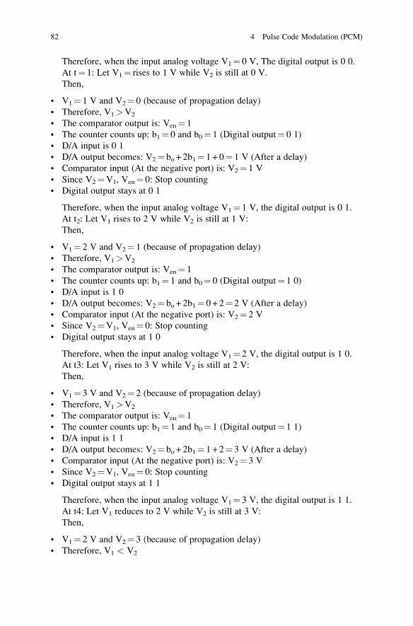
Therefore, when the input analog voltage V1¼ 0 V, The digital output is 0 0.
At t¼ 1: Let V1¼ rises to 1 V while V2 is still at 0 V.
Then,
• V1¼ 1 V and V2¼ 0 (because of propagation delay)
• Therefore, V1>V2
• The comparator output is: Ven¼ 1
• The counter counts up: b1¼ 0 and b0¼ 1 (Digital output¼ 0 1)
• D/A input is 0 1
• D/A output becomes: V2¼ bo + 2b1¼ 1 + 0¼ 1 V (After a delay)
• Comparator input (At the negative port) is: V2¼ 1 V
• Since V2¼V1, Ven¼ 0: Stop counting
• Digital output stays at 0 1
Therefore, when the input analog voltage V1¼ 1 V, the digital output is 0 1.
At t2: Let V1 rises to 2 V while V2 is still at 1 V:
Then,
• V1¼ 2 V and V2¼ 1 (because of propagation delay)
• Therefore, V1>V2
• The comparator output is: Ven¼ 1
• The counter counts up: b1¼ 1 and b0¼ 0 (Digital output¼ 1 0)
• D/A input is 1 0
• D/A output becomes: V2¼ bo + 2b1¼ 0 + 2¼ 2 V (After a delay)
• Comparator input (At the negative port) is: V2¼ 2 V
• Since V2¼V1, Ven¼ 0: Stop counting
• Digital output stays at 1 0
Therefore, when the input analog voltage V1¼ 2 V, the digital output is 1 0.
At t3: Let V1 rises to 3 V while V2 is still at 2 V:
Then,
• V1¼ 3 V and V2¼ 2 (because of propagation delay)
• Therefore, V1>V2
• The comparator output is: Ven¼ 1
• The counter counts up: b1¼ 1 and b0¼ 1 (Digital output¼ 1 1)
• D/A input is 1 1
• D/A output becomes: V2¼ bo + 2b1¼ 1 + 2¼ 3 V (After a delay)
• Comparator input (At the negative port) is: V2¼ 3 V
• Since V2¼V1, Ven¼ 0: Stop counting
• Digital output stays at 1 1
Therefore, when the input analog voltage V1¼ 3 V, the digital output is 1 1.
At t4: Let V1 reduces to 2 V while V2 is still at 3 V:
Then,
• V1¼ 2 V and V2¼ 3 (because of propagation delay)
• Therefore, V1 < V2
82 4 Pulse Code Modulation (PCM)
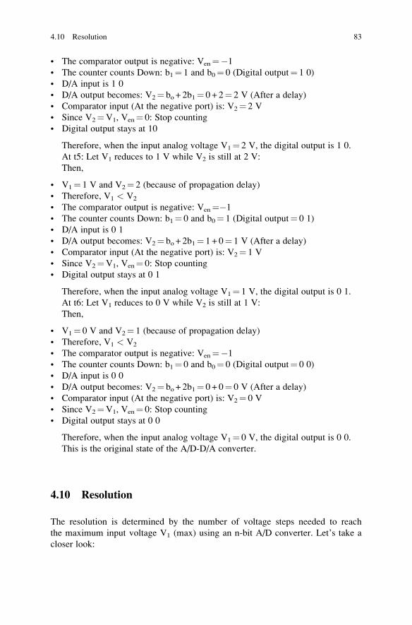
• The comparator output is negative: Ven¼�1
• The counter counts Down: b1¼ 1 and b0¼ 0 (Digital output¼ 1 0)
• D/A input is 1 0
• D/A output becomes: V2¼ bo + 2b1¼ 0 + 2¼ 2 V (After a delay)
• Comparator input (At the negative port) is: V2¼ 2 V
• Since V2¼V1, Ven¼ 0: Stop counting
• Digital output stays at 10
Therefore, when the input analog voltage V1¼ 2 V, the digital output is 1 0.
At t5: Let V1 reduces to 1 V while V2 is still at 2 V:
Then,
• V1¼ 1 V and V2¼ 2 (because of propagation delay)
• Therefore, V1 < V2
• The comparator output is negative: Ven¼�1
• The counter counts Down: b1¼ 0 and b0¼ 1 (Digital output¼ 0 1)
• D/A input is 0 1
• D/A output becomes: V2¼ bo + 2b1¼ 1 + 0¼ 1 V (After a delay)
• Comparator input (At the negative port) is: V2¼ 1 V
• Since V2¼V1, Ven¼ 0: Stop counting
• Digital output stays at 0 1
Therefore, when the input analog voltage V1¼ 1 V, the digital output is 0 1.
At t6: Let V1 reduces to 0 V while V2 is still at 1 V:
Then,
• V1¼ 0 V and V2¼ 1 (because of propagation delay)
• Therefore, V1 < V2
• The comparator output is negative: Ven¼�1
• The counter counts Down: b1¼ 0 and b0¼ 0 (Digital output¼ 0 0)
• D/A input is 0 0
• D/A output becomes: V2¼ bo + 2b1¼ 0 + 0¼ 0 V (After a delay)
• Comparator input (At the negative port) is: V2¼ 0 V
• Since V2¼V1, Ven¼ 0: Stop counting
• Digital output stays at 0 0
Therefore, when the input analog voltage V1¼ 0 V, the digital output is 0 0.
This is the original state of the A/D-D/A converter.
4.10 Resolution
The resolution is determined by the number of voltage steps needed to reach
the maximum input voltage V1 (max) using an n-bit A/D converter. Let’s take a
closer look:
4.10 Resolution 83
• For example, in a 2-bit A/D-D/A converter, there are 22¼ 4 levels (0–3). This is
to say that there are 22–1¼ 3 steps. Therefore, if V1 (max)¼ 3 V, the number of
steps needed to reach 3 V will be 3/(22–1)¼ 1 V per step.
• Similarly, in a 3-bit A/D-D/A converter, there are 23¼ 8 levels (0–7). This is to
say that there are 23–1¼ 7 steps. Therefore, if V1 (max)¼ 3 V, the number of
steps needed to reach 3 V will be 3/(23–1)¼ 3/7 V per step.
• Likewise, In an 8-bit A/D-D/A converter, there are 28¼ 256 levels (0–255). This
is to say that there ar or 28–1¼ 255 steps. Therefore, if V1 (max)¼ 3 V, the
number of steps needed to reach 3 V will be 3/(28–1)¼ 3/255 V per step.
From the above examples we see that the step size decreases rapidly as the
number of bits increases. This step size is known as resolution. In general, the
resolution is defined as,
R ¼ V1 maxð Þ2n � 1
Where, n is the number of bits.
Exercise 1
(a) Design an 8-Bit D/A converter with the following specifications:
• V2 (max)¼ 10 V
• Vref¼ 1 V
• Av¼ 1
(b) Estimate the resolution
Exercise 2
(a) Consider the previous exercise again and design an 8-Bit A/D converter.
(b) Estimate the resolution.
4.11 Binary Line Coding and Power Spectrum
The A/D output is a digital signal represented by a Binary 1 or a Binary 0. Before
these binary signals can be used, they are generally conditioned (converted into
different formats) before transmission. The process of formatting is called “Binary
Line Coding” [17]. Commonly used binary codes are:
• Non-return to Zero (NRZ)
• Return to Zero (RZ)
84 4 Pulse Code Modulation (PCM)

• Unipolar
• Bipolar
• Manchester
Etc.
We will consider some popular line coding, and evaluate their power spectrum.
4.11.1 Popular Binary Signaling Formats
Figure 4.19 shows the popular binary signals along with the clock. Here,
• Clock is a periodic waveform.
• Data is synchronized with the clock.
• NRZ data takes the full period of the clock. It does not return to zero along with
the clock. Its power spectrum is narrower than the clock.
• RZ data takes half the period of the clock. It returns to zero along with the clock.
Its power spectrum is wider than the NRZ data.
This brings us to a well-known topic known as “Fourier Transform”, which can
be used to determine the power spectrum associated with digital signals [xxx]. As
shown in Fig. 4.19, NRZ data has a period T. Therefore, the Fourier transform will
be as follows:
Fig. 4.19 Popular binary signals and the clock
4.11 Binary Line Coding and Power Spectrum 85

V ωð Þ ¼ðT
0
V tð Þ � e� jωtdt ð4:10Þ
P ωð Þ ¼ V2TSin ωT=2ð Þ
ωT=2
� �2ð4:11Þ
Where,
• V(t) is the time domain signal of the NRZ data
• V(ω) is the frequency domain expression of the NRZ data
• P(ω) is the power spectral density associated with the NRZ data
On the other hand, RZ data has a period T/2. Therefore, the Fourier transform
equation will be
V ωð Þ ¼ðT=2
0
V tð Þ � e� jωtdt ð4:12Þ
P ωð Þ ¼ V2TSin ωT=4ð Þ
ωT=4
� �2ð4:13Þ
Where,
• V(t) is the time domain signal of the RZ data
• V(ω) is the frequency domain expression of the RZ data
• P(ω) is the power spectral density associated with the RZ data
Figure 4.20 shows the power spectral densities of NRZ and RZ data, where P
(w) is plotted as a function fb/fc with T¼ 1/fc¼ 1. Notice that the first null for NRZ
Fig. 4.20 One sided power spectrum of NRZ and RZ data. The first null at fb/fc (T¼ 1/fc¼ 1)
determines the bandwidth. Note: fc¼ 1/T is constant and fb is variable
86 4 Pulse Code Modulation (PCM)

data is at fb (fb¼ 1/T) and RZ data is at 2fb (Period¼T/2). Therefore, NRZ data is
spectrally efficient. For this reason, NRZ data is more popular in wireless
communication.
4.12 Bit Rate
In A/D converter, the analog signal is sampled, quantized and converted into bit
streams by means of an n-bit A/D converter. Figure 4.21 shows a simplified version
to illustrate this.
The bit rate depends on:
• Sampling rate fs and
• Number of bits per sample (depends on A/D-D/A converter)
Therefore, the bit rate will be given by,
Rb ¼ n f s ð4:14Þ
Where,
• Rb¼Bit rate in bits per second
• fs¼ Sampling frequency in cycle per second (Hz)
• n¼Number of bits per sample
For example, a 1 kHz analog signal, sampled at fs¼ 8 kHz, will generate eight
samples per cycle of this analog signal. Therefore the bit rate will be
Rb¼ 8� 8¼ 64 kb/s.
Fig. 4.21 Illustration of PCM bit rate
4.12 Bit Rate 87

4.13 Bandwidth
We know from the Fourier Transform, and subsequently from NRZ and RZ data,
that the spectrum depends on the data type (NRZ, RZ, Bipolar, Manchester etc.).
After performing the one sided Fourier transform, we have noticed that the band-
width is primarily determined by the first “Null” of the Fourier Spectrum.
The total bandwidth associated with the data will be due to the two-sided
bandwidth, i.e., from first null first null, which is governed by the following Fourier
integral:
V ωð Þ ¼ðT
�T
V tð Þ � e� jωtdt ð4:15Þ
Figure 4.22 shows the corresponding two-sided spectral response. The total band-
width is given by the main lobe, determined by first null to first null, as shown in the
figure. In practical realization, the side lobes are filtered out, since they are small.
The bandwidth depends on:
• Bit rate in cycles per second (Hz)
• Two sided power spectral density and
• Signal formats: NRZ, RZ, . . .
Therefore, the bandwidth can be written as,
BW ¼ 2Rb ¼ 2n f s ð4:16Þ
For example, if the 64 kb/s data in the previous example is converted into NRZ data,
the bandwidth will be 2Rb¼ 2� 64 kb/s¼ 128 kHz. Note that the higher order
spectral components are filtered out.
Fig. 4.22 Bandwidth is determined by the main lobe, which is from the 1st null to 1st null. Side
lobes are filtered out since they are small
88 4 Pulse Code Modulation (PCM)

Problem 4.5
Given:
• fm¼ 1 kHz
• fs¼ 8 kHz (sampling rate)
• n¼ 8 bit/sample
• NRZ data
Find:
(a) Bit Rate
(b) Bandwidth
Solution:
(a) Rb¼ nfs¼ 8� 8¼ 64 kb/s
(b) BW¼ 2Rb¼ 2� 64 kb/s¼ 128 kHz
4.14 Conclusions
• We have presented a brief overview of PCM.
• Various PCM functional blocks such as Sampling, Linear and non-linear quan-
tization, A/D and D/A converters etc. were presented with examples.
• Method of estimating bit rate and bandwidth were presented.
References
1. H. Nyquist, Certain topics in telegraph transmission theory. Trans. AIEE 47, 617–644 (1928).Reprint as classic paper in: Proc. IEEE, Vol. 90, No. 2, Feb 2002
2. C.E. Shannon, A mathematical theory of communication. Bell Syst. Tech. J. 27, 379–423(1948). 623–656
3. B. Sklar, Digital Communications Fundamentals and Applications (Prentice Hall, Upper
Saddle River, 1988)
4. R.J. Marks II, Introduction to Shannon Sampling and Interpolation Theory (Springer, Berlin,1991)
5. R.J. Marks II (ed.), Advanced Topics in Shannon Sampling and Interpolation Theory (Springer,Berlin, 1993)
6. M. Unser, Sampling-50 years after Shannon. Proc. IEEE 88(4), 569–587 (2000)
7. E.T. Whittaker, On the functions which are represented by the expansions of the interpolation
theory. Proc. Royal Soc. Edinburgh, Sec. A 35, 181–194 (1915)
8. L.W. Couch II, Digital and Analog Communication Systems, 7th edn. (Prentice-Hall, Engle-
wood Cliffs, 2001). ISBN 0-13-142492-0
9. A.S. Sedra, K.C. Smith, Microelectronic Circuits, 6th edn. (Oxford University Press,
New York, 2010). ISBN 978-0-19-532303-0
10. A. Gersho, Quantization, IEEE Communications Society Magazine, pp. 16–28, Sept. 1977.
doi:10.1109/MCOM.1977.1089500
References 89

11. B. Widrow, A study of rough amplitude quantization by means of Nyquist sampling theory.
IRE Trans. Circuit Theory CT-3, 266–276 (1956). doi:10.1109/TCT.1956.1086334
12. R.M. Gray, D.L. Neuhoff, Quantization. IEEE Trans. Inform. Theory IT-44(6), 2325–2383(1998). doi:10.1109/18.720541
13. B. Smith, Instantaneous companding of quantized signals. Bell Syst. Tech. J. 36, 653–709(1957)
14. H. Kaneko, A unified formulation of segment companding laws and synthesis of codecs and
digital compandors. Bell Syst. Tech. J. 49, 1555–1558 (1970)
15. W.R. Bennett, Spectra of quantized signals. Bell Syst. Tech. J. 27, 446–472 (1948)
16. R.M. Gray, D.L. Neuhoff, Quantization. IEEE Trans. Inform. Theory IT-44(6), 2325–2383(1998). doi:10.1109/18.720541
17. D.R. Smith, Digital Transmission Systems (Van Nostrand Reinhold, New York, 1985). ISBN
0442009178
90 4 Pulse Code Modulation (PCM)

Chapter 5
Time Division Multiplexing (TDM)
Topics
• Introduction
• TDM Structure
• TDM Frame and Frame Hierarchy
• Frame Synchronization
• North American TDM Standard for Land Telephone System
• The T1(DS1) System
• TDMA for Wireless Communications
• TDMA Frame and Frame Hierarchy
• TDMA BER Performance Analysis
5.1 Introduction
Time-division multiplexing (TDM) is a method of transmitting and receiving k
independent signals over a single transmission channel [1–3]. Figure 5.1 provides a
simplified block diagram to illustrate the concept. In this scheme, the TDM at the
transmit side is known as multiplexer and the TDM at the receive side is known as
de-Multiplexer. The TDM at the transmit side assigns k-channels in pre-assigned
time slots, where k-time slots constitute a frame. Frame synchronization bits are
inserted to identify the “Start’ and Stop” of the frame. The synchronization bit
pattern is unique and used for frame synchronization. The TDM at the receive side,
known as the de-multiplexer, separates the incoming composite signal into k
parallel streams as shown in the figure. Both multiplexer and de-multiplexer are
synchronized by a common clock to receive data in accordance with the transmit
sequence.
The limitation in TDM scheme is that, when one signal occupies the channel,
other signals are idle. Therefore there is a delay in TDM system. As a result, the
© Springer International Publishing Switzerland 2015
S. Faruque, Radio Frequency Source Coding Made Easy, SpringerBriefsin Electrical and Computer Engineering, DOI 10.1007/978-3-319-15609-5_5
91

number of signals that can be time shared is limited. Another limitation is the
channel bandwidth. For example, ten parallel data streams, having 10 k b/s data
stream each, will produce a 100 k b/s data stream after multiplexing, requiring a
wider transmission bandwidth.
Applications include:
• North American digital telephony, where 24 channels are time shared, one at a
time [1].
• European digital telephony, where 32 channels are time shared, one at a time [1].
We will revisit this topic in more details in this chapter.
Problem 5.1
Given:
• North American PCM System
• 24 users multiplexed to form a single composite bit stream
• Frame length¼ 125 μs (micro second)
• Each user generates 64 kb/s data
(a) Calculate the composite bit rate after multiplexing
(b) Show the multiplexing and de-multiplexing scheme
Fig. 5.1 Time division multiplexing. K data streams are time shared in a single transmission
channel, one at a time. Switches are controlled at both ends synchronously by means of a clock.
Data is formatted in a frame. Synchronization bits are inserted to synchronize the frame
92 5 Time Division Multiplexing (TDM)

Solution:
(a) Total Bit Rate after Multiplexing:
• The total bit rate after multiplexing¼ 24� 64 k¼ 1.536 Mb/s.
• This is known as: “Digital Signal-1 or DS1”.
• When the DS1 signal (1.536 MHz) is transmitted through a transmission line, the
transmission line is known as “T1 link”. See figure below:
(b) Multiplexing and De-Multiplexing Scheme:
With the advent of cellular technology [4–6], the TDM system was further
extended to support multiple users in the wireless domain known as TDMA
(Time Division Multiple Access). Figure 5.2 shows the basic concept used in
wireless communications. In this scheme, the radio transmitter combines data
from several users according to the TDM protocol and transmits one at a time in
a cyclic fashion. The receiver recovers the clock for synchronization and delivers
the data to the respective recipient one at a time. Applications include:
Fig. 5.2 TDMA concept for wireless communications. At the transmitter, k users are time shared
and transmitted by a radio, one at a time. At the receiver, the clock is recovered from the received
data for synchronization
5.1 Introduction 93
• North American second generation (2G) cellular telephony. In this scheme, each
30 kHz RF (Radio Frequency) channel is time shared by three users, one at a
time, in a cyclic fashion [4–6].
• GSM cellular system, where eight users can time share a 200 kHz RF channel
one at a time in a cyclic fashion [7–10].
We will revisit this topic later in more details in this chapter.
5.2 North American TDM in Digital Telephony
5.2.1 The Basic TDM Structure
The North American TDM [1–3] for digital telephony is a hierarchical system
which supports 24 PCM channels per frame as shown in Fig. 5.3, where each PCM
is a 64 kb/s channel.
At the transmit side (Multiplexing):
• 24-channels are interleaved in preassigned time slots
• 24-channels form a frame
• Frame bits are inserted to identify the “Start’ and Stop” of the frame
• These frame bit pattern is unique and used for frame synchronization. (a topic
yet to be discussed)
• The frame length¼ 125 μs (ITU Standard)
• Each frame contains 24 channels
• Each channel is also called DS-0 (Digital Signal-0)
• DS-0 Rate¼ 64 kbps
• Each DS-0 channel has 8-bits
• 1 Sync bit is added at the end
• Total Number of bits/Frame¼ (8� 24) + 1¼ 193 bits
• Bit rate¼ 193/125 μs¼ 1.544 Mb/s
Fig. 5.3 The North American TDM system for digital telephone system. 24 PCM channels form a
125 μs frame
94 5 Time Division Multiplexing (TDM)
At the receive side (DE multiplexing):
• The De-multiplexer receives successive frames
• Each frame has a “header frame bit pattern” which is unique
• The De-multiplexer synchronizes with the frame bit pattern and recovers all the
channels and puts them in the right order
There are two types of frame structure:
• Distributed, where Frame synchronization bits are inserted one at a time at the
beginning or at the end of the frame. Each frame contains data + 1 frame-bit.
• Bunched, where All the frame sync. bits are inserted in one time slot.
Both Distributed and Bunched structure have advantages and disadvantages.
5.2.2 Distributed Frame Structure
A distributed frame is constructed by distributing 12 sync bits among 12 frames,
1 sync bit per frame. This is shown in Fig. 5.4. In this scheme, the distributed frame
structure is specified as follows:
• Frame length¼ 125 μs• One Frame contains 24-Channels and a frame bit: The total number of bits per
frame is
Fig. 5.4 Distributed frame structure. 12 sync bits are distributed among 12 frames
5.2 North American TDM in Digital Telephony 95
F ¼ 24� 8þ 1 ¼ 193 bits per frame
• A Super Frame (Multi Frame) contains 12 Frames:
S ¼ 12� 1, 193 ¼ 2, 316 bits per super frame
Advantages:
• Immune to burst errors. Because frame bits are distributed
• Synchronizer has enough time to compute
Disadvantages:
• It takes a long time to synchronize. Because all the sync. bits are needed in the
computation.
5.2.3 Bunched Frame Structure
A bunched frame is constructed by placing 12 sync bits in one time slot. This is
shown in Fig. 5.5.
In this scheme, the bunched frame is specified as follows:
• A Channel contains M-bits (e.g., 8-bits)
• One Frame contains 12-Channels
Fig. 5.5 Bunched frame structure.12 sync bits are bunched together at the end of the super frame
96 5 Time Division Multiplexing (TDM)

• F¼ 24� 8¼ 192 bits per frame
• A Super Frame (Multi Frame) contains 12-Frames + 12 sync bits bunched
S ¼ 192 � 12 þ 12 ¼ 2, 316 bits per super frame
Therefore the total number of bits is the same in both cases
Advantages and Disadvantages of Bunched Frame Structure:
Advantages:
Faster synchronization if sync. bits are inserted in every frame.
• Sync. Maintenance in the frame level
Disadvantages:
• Poor performance in jamming. Because frame bits are bunched.
5.3 European TDM in Digital Telephony
The European TDM [1, 2] for digital telephony supports 32 TDM channels per
frame, where each TEM channel is a 64 kb/s channel. The frame and super frame
structure is shown in Fig. 5.6. At the transmit side (Multiplexing):
• 32-channels are interleaved in preassigned time slots, 8-bits per time slot.
• 32-channels form a frame.
• Time slot 1is reserved for synchronization.
• Time slot 16 is reserved for signaling.
Fig. 5.6 The European frame and super frame structure. There are 32 time slots per frame. Time
slot 18is reserved for synchronization. Time slot-16 is reserved for signaling. Rest of the time slots
are used for data. The super frame contains 16 frames
5.3 European TDM in Digital Telephony 97

• Rest of the time slots are for data.
• DS-0 Rate¼ 64 kbps.
• Each DS-0 channel has 8-bits.
• Total Number of bits/Frame¼ 8� 32¼ 256 bits.
• The frame length¼ 125 μs.• bit rate¼256/125 μs¼ 2,048 Mb/s.
At the receive side (DE multiplexing):
• The De-multiplexer receives successive frames
• Each frame has a “header frame synchronization pattern” which is unique
• The De-multiplexer synchronizes with the frame bit pattern and recovers all the
channels and puts them in the right order
5.4 Frame Synchronization
5.4.1 Synchronization Process
There are two modes of operation in frame synchronization circuits:
• Mode-1: Frame Search Mode or Frame Acquisition Mode
• Mode-2: Frame Maintenance Mode
In Frame Acquisition Mode:
• It searches through the candidate frames
• Looks for the unique frame pattern
• It keeps looking until a valid pattern is detected
• If valid, it accepts the frame, if not, it rejects the frame
• The accept/reject criteria is based on a “Correlation Process”
In Frame Maintenance Mode:
• After synchronization, each frame is continuously monitored and a frame quality
indicator is generated as “Frame Error Rate (FER)”
• If FER�Threshold, it maintains the synchronization
• If FER>Threshold, it declares loss of sync and
• The synchronization process begins again
5.4.2 Estimation of Frame Error Rate
The estimation of frame error rate is based on a correlation process. In this process,
it performs the following:
98 5 Time Division Multiplexing (TDM)

• It compares k-bit sync word with a k-bit data block by means of a sliding
correlator as shown in Fig. 5.7.
• It begins with the k-bit sync word and compares with a k-bit word. If it matches,
the receiver declares a success and begins tracking. If not, the sync word is
shifted by one bit and compared with the next k-bit data word for a possible
match.
Fig. 5.7 Sliding correlator. The sync word is compared with the received data for correlation, as it
slides
5.4 Frame Synchronization 99
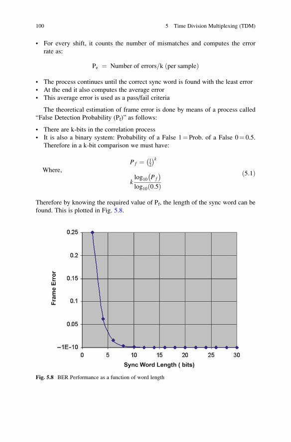
• For every shift, it counts the number of mismatches and computes the error
rate as:
Pe ¼ Number of errors=k per sampleð Þ
• The process continues until the correct sync word is found with the least error
• At the end it also computes the average error
• This average error is used as a pass/fail criteria
The theoretical estimation of frame error is done by means of a process called
“False Detection Probability (Pf)” as follows:
• There are k-bits in the correlation process
• It is also a binary system: Probability of a False 1¼ Prob. of a False 0¼ 0.5.
Therefore in a k-bit comparison we must have:
P f ¼ 12
� �kWhere,
klog10 P f
� �log10 0:5ð Þ
ð5:1Þ
Therefore by knowing the required value of Pf, the length of the sync word can be
found. This is plotted in Fig. 5.8.
Fig. 5.8 BER Performance as a function of word length
100 5 Time Division Multiplexing (TDM)

5.5 North American TDM Hierarchy
The TDM hierarchy is composed of a multi-frame structure known as super frame
as shown in Fig. 5.9.
• The super frame contains 12 Frames
• Each frame has a sync bit
• Total number of sync bit¼ 12
• These 12 sync bits are used to synchronize the frames and multi frames
• Number of bits/multi frame¼ 193� 12¼ 2,316 bits
• Fraction used by Sync¼ 12/2,316¼ 0.005181
• This gives rise to Frame Error Rate, which is given by, FER, also known as the
probability of frame error rate:
P f ¼ 0:5ð Þ12 ¼ 2:44� 10�4 ð5:2Þ
DS-1 (T1) Rate can be estimated as:
• Number of information bits/Frame¼ 193 bits/frame
• Frame Length¼ 125 μs• Bit Duration Tb¼ 125 μs/193• DS-1 Rate¼ 1/Tb¼ 1.544 Mbps
Higher rates can be obtained from DS-1 by successive multiplexing as shown in
Fig. 5.10. These rates are estimated as follows:
• DS2 Rate ¼ 4� DS1 ¼ 4� 1:544 Mbps ¼ 6:312 Mbps
• DS3 Rate ¼ 7� DS2 ¼ 7� 6:312 Mbps ¼ 44:736 Mbps
• DS4 Rate ¼ 6� DS3 ¼ 6� 44:736 Mbps ¼ 274:176 Mbps
• DS5 Rate ¼ 2� DS4 ¼ 2� 274:176 Mbps ¼ 560:160 Mbps
Fig. 5.9 The North American TDM multi frame structure. (a) The frame. (b) Super frame
containing 12 frames
5.5 North American TDM Hierarchy 101

5.6 Time Division Multiple Access (TDMA)
5.6.1 The North American TDMA
The North American TDMA is a narrow band (30 kHz) mobile cellular system,
which supports dual-mode (1G & 2G) cellular communication systems [4–7]. Since
the transmission bandwidth is only 30 kHz, the digitized 64 kb/s voice data is first
compressed by means of a Vocoder, encoded for error control coding, modulated
and finally transmitted over the air as depicted in Fig. 5.11.
At the transmit side, the voice is first digitized and then compressed by means of
a vocoder to form a low bit rate data stream. The compressed data is then encoded
by means of rate 1/2 convolutional encoder and interleaved. Together with frame
overhead, the composite bit rate becomes 16.2 kb/s for each user. This 16.2 kb/s
data is distributed within two 6.66 ms time slots, 8.1 kb/s data per time slot. Three of
these 16.2 kb/s subscriber data are combined to form a 48.6 kb/s TDMA frame.
Fig. 5.10 The North American TDM hierarchy
Fig. 5.11 The basic land-mobile cellular communication system
102 5 Time Division Multiplexing (TDM)
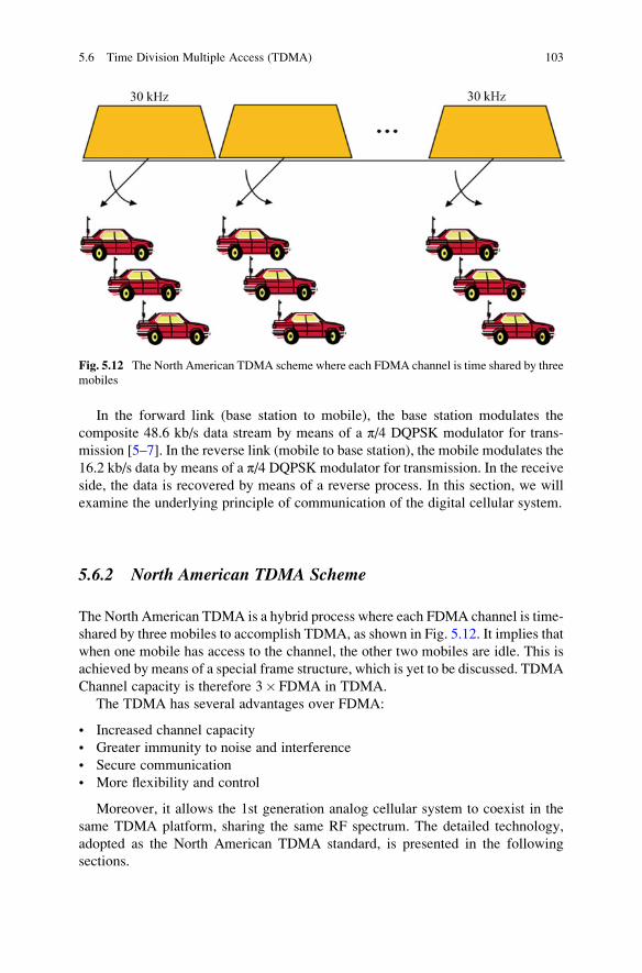
In the forward link (base station to mobile), the base station modulates the
composite 48.6 kb/s data stream by means of a π/4 DQPSK modulator for trans-
mission [5–7]. In the reverse link (mobile to base station), the mobile modulates the
16.2 kb/s data by means of a π/4 DQPSK modulator for transmission. In the receive
side, the data is recovered by means of a reverse process. In this section, we will
examine the underlying principle of communication of the digital cellular system.
5.6.2 North American TDMA Scheme
The North American TDMA is a hybrid process where each FDMA channel is time-
shared by three mobiles to accomplish TDMA, as shown in Fig. 5.12. It implies that
when one mobile has access to the channel, the other two mobiles are idle. This is
achieved by means of a special frame structure, which is yet to be discussed. TDMA
Channel capacity is therefore 3� FDMA in TDMA.
The TDMA has several advantages over FDMA:
• Increased channel capacity
• Greater immunity to noise and interference
• Secure communication
• More flexibility and control
Moreover, it allows the 1st generation analog cellular system to coexist in the
same TDMA platform, sharing the same RF spectrum. The detailed technology,
adopted as the North American TDMA standard, is presented in the following
sections.
Fig. 5.12 The North American TDMA scheme where each FDMA channel is time shared by three
mobiles
5.6 Time Division Multiple Access (TDMA) 103
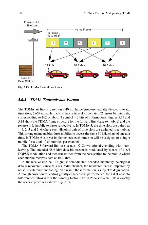
5.6.3 TDMA Transmission Format
The TDMA air link is based on a 40 ms frame structure, equally divided into six
time slots, 6.667 ms each. Each of the six time slots contains 324 gross bit intervals,
corresponding to 162 symbols (1 symbol¼ 2 bits of information). Figures 5.13 and
5.14 show the TDMA frame structure for the forward link (base to mobile) and the
reverse link (mobile to base) respectively. In TDMA-3, the time slots are paired as
1–4, 2–5 and 3–6 where each disjoints pair of time slots are assigned to a mobile.
This arrangement enables three mobiles to access the same 30 kHz channel one at a
time. In TDMA-6 (not yet implemented), each time slot will be assigned to a single
mobile for a total of six mobiles per channel.
The TDMA-3 forward link uses a rate 1/2 Convolutional encoding with inter-
leaving. The encoded 48.6 kb/s data bit stream is modulated by means of a π/4DQPSK modulation and then transmitted from the base station to the mobile where
each mobile receives data at 16.2 kb/s.
At the receive side the RF signal is demodulated, decoded and finally the original
data is recovered. Since this is a radio channel, the recovered data is impaired by
noise, interference and fading. As a result, the information is subject to degradation.
Although error control coding greatly enhances the performance, the C/I (Carrier to
Interference ratio) is still the limiting factor. The TDMA-3 reverse link is exactly
the reverse process as shown Fig. 5.14.
Forward Link48.6 kb/s
6.66 msTime Slot
CellularBase Station
16.2 kb/s 16.2 kb/s 16.2 kb/s
40 ms Frame
1 2 3 4 5 6
Fig. 5.13 TDMA forward link format
104 5 Time Division Multiplexing (TDM)
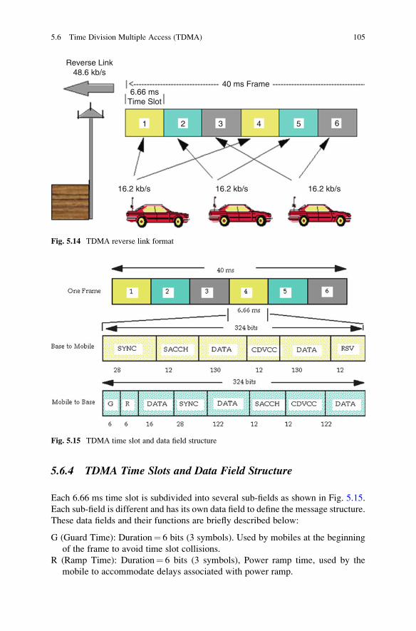
5.6.4 TDMA Time Slots and Data Field Structure
Each 6.66 ms time slot is subdivided into several sub-fields as shown in Fig. 5.15.
Each sub-field is different and has its own data field to define the message structure.
These data fields and their functions are briefly described below:
G (Guard Time): Duration¼ 6 bits (3 symbols). Used by mobiles at the beginning
of the frame to avoid time slot collisions.
R (Ramp Time): Duration¼ 6 bits (3 symbols), Power ramp time, used by the
mobile to accommodate delays associated with power ramp.
Reverse Link48.6 kb/s
6.66 msTime Slot
16.2 kb/s 16.2 kb/s 16.2 kb/s
40 ms Frame
1 2 3 4 5 6
Fig. 5.14 TDMA reverse link format
Fig. 5.15 TDMA time slot and data field structure
5.6 Time Division Multiple Access (TDMA) 105

SYNC.: Duration¼ 28bits (14 symbols). Used by both base & mobiles for time slot
synchronization, equalizer training and time slot identification.
DATA: User information, compressed by vocoder, rate 1/2 convolutionally
encoded, interleaved data, Used by base & mobiles. This time slot is also shared
by FACCH (Fast Associated Control Channel).
FACCH: Fast Associated Control Channel. Used for signaling message exchange
between the base & the mobile. No message is transmitted during this process.
As a result, there is a minor impact on voice quality. FACCH is generally used
for hand-off messaging. Many other messaging requiring immediate responses is
also sent via FACCH. Error protection is the same as data.
SACCH: Slow Associated Control Channel. A dedicated continuous channel used
for signaling message exchange between the base & the mobile. SACCH is
present in all designated slots regardless of the presence of data or FACCH. It is
a 12 bit (6 symbol) field, rate 1/2 convolutionally encoded and interleaved.
CDVCC: Coded Digital Verification Color Code. A 12 bit (6 symbol) data field. It
is generated from an 8 bit DVCC (Digital Verification Color Code) having
255 distinct values. The DVCC is analogous to the SAT frequencies in AMPS
system. It is used to distinguish a serving channel from a reuse channel. The
12 bit CDVCC generated from the 8 bit DVCC field by adding four
protection bits.
Problem 5.2
Given:
• Frame length¼ 40 ms (Figure below).
• The frame contains Six time slots and supports three users.
• Each user originates 16.2 kbps data.
Find:
(a) A suitable multiplexing structure
(b) The composite data rate in the channel
(c) Number of bits/Frame
Solution:
(a) We have 3 users and 6-Time Slots. Therefore we can assign 2-time slots/user:
• User-1: Time slot 1 and 4
• User-2: Time slot 2 and 5
• User-3: Time slot 3 and 6
106 5 Time Division Multiplexing (TDM)

(b) Composite Data Rate:
16.2 kbps/user� 3¼ 48.6 kbps
(c) Number of bits/Frame¼ Frame length /Bit duration
¼40 ms/(1/48.6 kbps)¼ 1,944 bits/Frame
Problem 5.3
Consider the previous problem again and construct a de-multiplexing scheme to
recover three users.
Answer:
5.6 Time Division Multiple Access (TDMA) 107

5.7 Global System for Mobile Communication (GSM)
5.7.1 GSM TDMA Scheme
GSM (Groupe Special Mobile) also known as Global System for Mobile Commu-
nications, is a second generation (2G) digital cellular communication standard
developed in Europe [7–10]. In GSM, a given frequency band is divided into
200 KHz per carrier, where each carrier is time shared by eight users as depicted
in Fig. 5.16.
Since each RF carrier frequency is time shared between 8 users, there are 8 time
slots in the GSM frame. According to the GSM communication protocol, the time
slot is assigned to a mobile during the channel assignment Session. Therefore, when
one mobile is active, other mobiles remain idle. Each mobile waits for their turn.
5.7.2 GSM TDMA Frame (4.615 ms)
The GSM frame is constructed by multiplexing 8 time slots as shown in Fig. 5.17.
It has the following design specifications:
• Frame duration: 4.615 ms
• Frame length: 8 time slots
• Duration of Time slot¼ 0.576875 ms¼ 0.577 ms
• Number of bits per time slot: 156.25 bits
• Bit rate: 270.833 kb/s
Fig. 5.16 The European GSMTDMA scheme. Each 200 kHz channel is time shared by eight users
108 5 Time Division Multiplexing (TDM)

5.7.3 GSM TDMA Frame Hierarchy
GSM Multiframe
The GSM TDMA hierarchy is composed of two types of multi-frame structure
known as:
• Control Multi-Frame for messaging and signaling (51 time slots, 0.577 ms/time
slot)
• Traffic Multi-Frame for voice and data (26 time slots, 0.577 ms/time slot)
The Control multi-frame, shown in Fig. 5.18, has 51 time slots-Called control
multiframe, composed of 51 bursts in duration of 235.4 ms. The time slots are used
for messaging and control function such as channel assignment, handoff, paging
etc.
The Traffic multi-frame, also shown in Fig. 5.18, has 26 time slots—Called
traffic multiframe, composed of 26 bursts in duration of 120 ms. These time slots
are used voice and data communication.
GSM Superframe (6.12 s)
GSM superframe is constructed by multiplexing several multiframes. There are two
schemes in the superframe:
• 51 traffic multiframes and 26 control multiframes. OR
• 26 traffic multiframes and 51 control multiframes.
When the scheme interchanges, the different number of traffic and control
multiframes within the superframe, the time interval within the superframe remains
the same. See Fig. 5.18a, b.
Fig. 5.17 GSM TDMA frame structure. Eight time slots multiplexed to construct a frame
5.7 Global System for Mobile Communication (GSM) 109
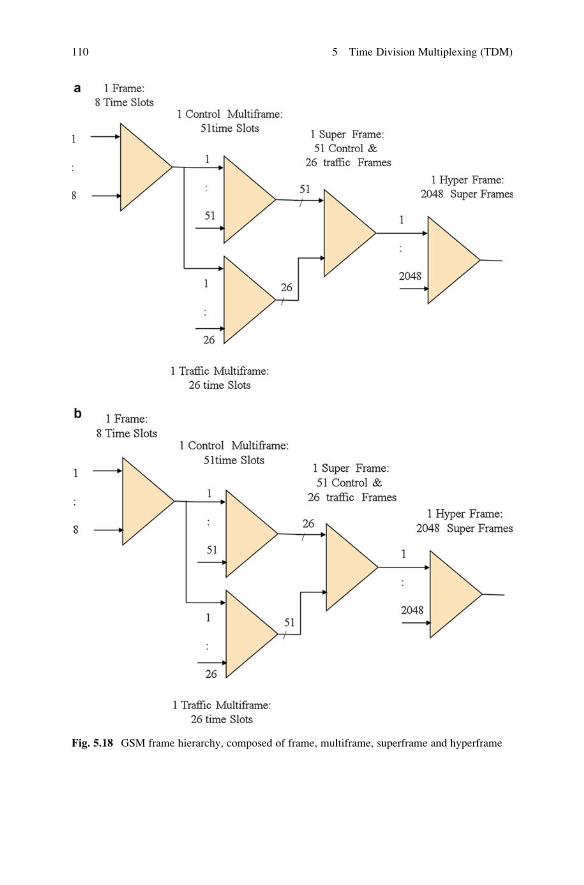
Fig. 5.18 GSM frame hierarchy, composed of frame, multiframe, superframe and hyperframe
110 5 Time Division Multiplexing (TDM)

GSM Hyperframe
GSM hyperframe is constructed by multiplexing 2,048 Super Frames. The
hyperframe is used to:
• Maintain different schedules in order.
• Synchronize and maintain encryption.
• Synchronize frequency hopping between the transmitter and the receiver so that
they hop to a new frequency at the same time. This is a low frequency hopping
feature in GSM.
5.8 TDMA Performance
5.8.1 Uncoded and Coded BER
Performance analysis provides an early prediction of potential problems and offers
successful deployment of cellular networks. For TDMA, this is generally accom-
plished by means of estimating the channel BER (Bit Error Rate). We examine this
by using a simplified channel model with and without coding. An exact analysis of
this problem is fairly complex. However, an approximation can be made using the
following assumptions:
• The radio is assumed to be a coded, interleaved communication system
• The interleaver depth is infinite so that the error bits are evenly distributed
• Rate ½ convolutional encoding with constraints length¼ 5
• Viterbi decoder on the receiver side
• M-ary PSK modulation/demodulation with M¼ 4
A model of the receiver that closely approximates the above set of assumptions
is shown in Fig. 5.19. We further assume that the receiver is operating in additive
white Gaussian noise (AWGN).
For equally likely coherently detected M-ary signaling, the probability of sym-
bol error is given by [11–14]:
Fig. 5.19 TDMA channel model for performance analysis
5.8 TDMA Performance 111
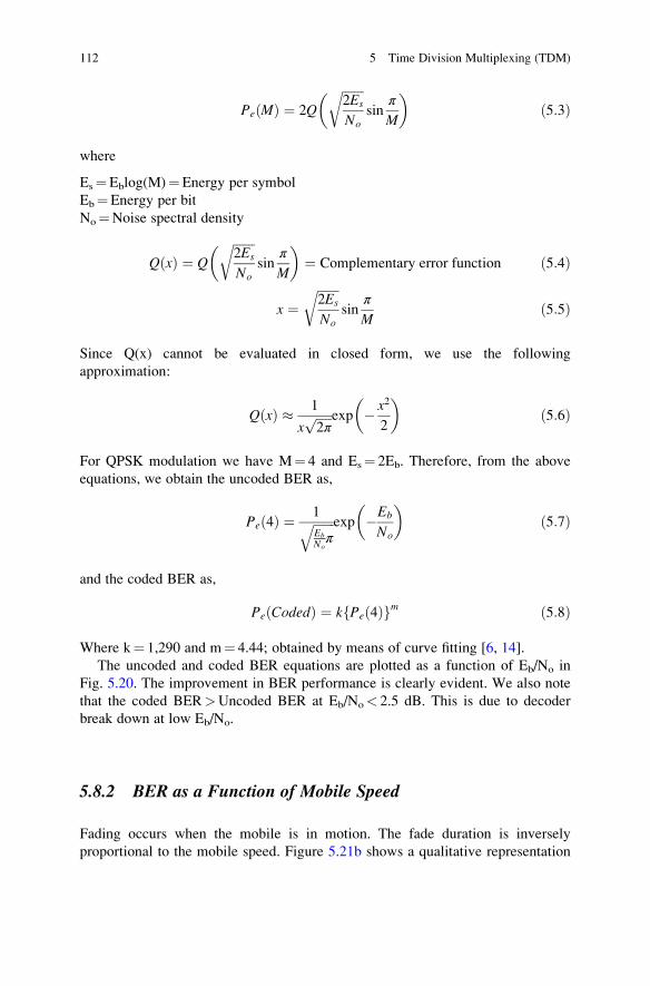
Pe Mð Þ ¼ 2Q
ffiffiffiffiffiffiffi2Es
No
rsin
π
M
� �ð5:3Þ
where
Es¼Eblog(M)¼Energy per symbol
Eb¼Energy per bit
No¼Noise spectral density
Q xð Þ ¼ Q
ffiffiffiffiffiffiffi2Es
No
rsin
π
M
� �¼ Complementary error function ð5:4Þ
x ¼ffiffiffiffiffiffiffi2Es
No
rsin
π
Mð5:5Þ
Since Q(x) cannot be evaluated in closed form, we use the following
approximation:
Q xð Þ � 1
xffiffiffiffiffi2π
p exp � x2
2
� �ð5:6Þ
For QPSK modulation we have M¼ 4 and Es¼ 2Eb. Therefore, from the above
equations, we obtain the uncoded BER as,
Pe 4ð Þ ¼ 1ffiffiffiffiffiffiffiEb
Noπ
q exp �Eb
No
� �ð5:7Þ
and the coded BER as,
Pe Codedð Þ ¼ k Pe 4ð Þf gm ð5:8Þ
Where k¼ 1,290 and m¼ 4.44; obtained by means of curve fitting [6, 14].
The uncoded and coded BER equations are plotted as a function of Eb/No in
Fig. 5.20. The improvement in BER performance is clearly evident. We also note
that the coded BER>Uncoded BER at Eb/No< 2.5 dB. This is due to decoder
break down at low Eb/No.
5.8.2 BER as a Function of Mobile Speed
Fading occurs when the mobile is in motion. The fade duration is inversely
proportional to the mobile speed. Figure 5.21b shows a qualitative representation
112 5 Time Division Multiplexing (TDM)

of fade depth as a function of fade duration. This can be estimated by means of the
following equation [5]:
t � 0:264
vð5:9Þ
Where t is the fade duration and v is the velocity of the mobile. The above equation
is plotted in Fig. 5.21a, which shows that fade duration decrease with increasing
mobile speed. We also note that fade duration¼ 6.6 ms @ 40 km/h which is exactly
one time slot of the North American TDMA frame (40 ms/6¼ 6.6 ms). This implies
that the entire time slot is subject to impairments. Since the bit rate is 48.6 kb/s, the
6.6 ms time slot translates into 120 bits. In other words, 120 bits will be jammed @
40 km/h. However, it does not mean that there will be an outage. This is due to the
0.06
0.05
0.04
0.03
Fad
e D
ura
tio
n (
sec.
)
a b
0.02
0.01
00 20 30 40
Velocity (km/h)
t=0.264/V sec.
80 10030dB
FadeDepth(dB)
0 dBFade Duration (sec.)
Fig. 5.21 (a) Fade duration as a function of mobile speed and (b) Qualitative representation of
fade depth as a function of fade duration
1
0.011 2 3 4 5 6 7 8 9 10 11 12
Uncoded
Conv. Enc.
13
Eb/No (dB)B
ER
0.0001
1E-06
1E-08
1E-10
1E-12
Fig. 5.20 TDMA BER performance with and without coding
5.8 TDMA Performance 113

fact that survivability depends on fade duration, depth of fading and the built-in
error control coding.
We will now estimate the BER performance by means of the illustration shown
in Fig. 5.17b where the depth of fading is shown as a function of fade duration. We
see that a deep fade is associated with a short duration while a shallow fade is
associated with long duration. This implies that a deep fade (short duration) is less
vulnerable due to the presence of FECC, which will detect and correct errors.
Likewise, a shallow fade (long duration) is also less vulnerable since Eb/No will
be adequate to achieve the BER objective. It follows that a fading that is neither
shallow nor deep is a point of concern.
The uncoded BER that follows the above logic can be expressed as
Pα 4ð Þ ¼ αffiffiffiffiffiffiffiEb
Noπ
q exp �Eb
Noα
� �ð5:10Þ
and the coded BER as
Pα Codedð Þ ¼ k Pα 4ð Þf gm ð5:11Þ
Where 0 < α < 1 is the fractional jamming (interference), k¼ 1,290 and m¼ 4.44
[xx]. Figure 5.22 shows the BER as a function of fractional interference for several
values of Eb/No. A close inspection reveals that a worst-case performance appears
around 20 % fractional jamming. Therefore the fraction of the time slot that is being
jammed is 6.6 ms� 0.20¼ 1.32 ms. The 1.32 ms fractional jamming corresponds to
a mobile velocity of 20 km/h. Therefore, in IS-54/136, the worst-case performance
can be expected at mobile velocity of 20 km/h. The survivability then depends on
Eb/No.
Fractional Interference1
0.10.2 0.4 0.6 0.8 10
Eb/No=4dB
Eb/No=6dB
Eb/No=8dB
Eb/No=10dB
0.01
0.001
0.0001BE
R
0.00001
0.000001
0.0000001
Fig. 5.22 BER as a function of fractional jamming
114 5 Time Division Multiplexing (TDM)

Problem 5.4
Given:
A 64 kb/s serial data is converted into 8 parallel streams. What is the output bit
rate after serial to parallel conversion?
Solution:
The output bit rate after 1:8 serial to parallel conversion will be 64 kbps/8¼ 8 kb/s/
as shown in the figure below:
Problem 5.5
Given:
Eight parallel data streams, having 8 kb/s each, is parallel to serial converted to
form a composite bit stream. What is the output bit rate after 8:1 parallel to serial
conversion?
Solution:The output bit rate after 8:1 parallel to serial conversion will be 8 kb/s� 8¼ 64 kb/
s/ as shown in the figure below:
5.9 Conclusions
• Defined TDM and TDMA
• Described TDM frame and frame hierarchy used in North American and
European Land Telephone System
• Illustrated Frame Synchronization Process
• Reviewed North American TDMA and European GSM TDMA System used in
Wireless Communications
5.9 Conclusions 115
• Illustrated TDMA Frame and Frame Hierarchy
• Presented TDMA BER Performance Analysis
QUIZ:
1. A PCM system needs to process analog signals ranging from 300 to 3,400 Hz.
What type of band limiting filter is needed? (Select one)
a. Band reject filter
b. Band pass filter
c. Low pass filter
d. High pass filter
2. The filtered signal in problem-1 is sampled at 8 kHz. Each sample is then
converted into 8bits. What is the output bit rate?
a. 32 kb/s
b. 64 kb/s
c. 128 kb/s
d. 256 kb/s
3. According to the Nyquist theorem, the sampling frequency should be:
a. More than the analog frequency
b. More than twice the analog frequency
c. Equal to the analog frequency,
4. In an 8-bit PCM, the number of quantization levels are given by:
a. 255
b. 256
c. 257
5. In an 8-bit PCM, the number of quantization steps are given by:
a. 255
b. 256
c. 257
6. In an 8-bit PCM, the voltage (V) per step is given by:
a. V/255
b. V/256
c. 2V/255
d. 2V/256
7. A PCM signal is band limited up to 3.4 kHz and then sampled at 8,000 times
per second. If each sample is converted into 8-bits, What is the output bit rate?
a. 34 kb/s
b. 64 kb/s
c. 128 kb/s
116 5 Time Division Multiplexing (TDM)

8. A given residential area has 1,000 homes. Each home has a land-line telephone.
If each telephone originates 64 kb/s data, construct a PCM hierarchical system
to support the traffic.
Answer:
9. A distributed frame structure is constructed having 40 ms per frame, sync
word¼ 12 bits. Specify the sync time.
Answer:
10. A full duplex communication system provides one of the following:
a. One way communication
b. Two way communication, one at a time
c. Two way communications, simultaneously
d. None of the above
11. A TDM wireless communication system combines data from three users to
form a composite data stream. If each user generates 16.2 kb/s data, what is the
composite bit rate?
a. 16.2 kb/s
b. 32.4 kb/s
c. 48.6 kb/s
12. A TTDMA frame structure has the following specifications:
a. Frame length¼ 40 ms
b. Bit rate¼ 48.6 kb/s
c. Sync. Word¼ 48 bits (at the beginning of the frame).
Find:
(a) The probability of false detection.
(b) The maximum sync. time needed to validate the frame. (Assume sliding
correlator)
Answer:
13. The North American TDMA standard allocates 30 kHz per channel. In the FCC
allocated frequency band is 12.55 MHz, calculate the number of users
supported by the band.
Answer:
14. The GSM standard allocates 200 MHz per channel If each channel supports
eight users one at a time, calculate the total number of users that can be
supported.
Answer:
5.9 Conclusions 117

References
1. D.R. Smith, Digital Transmission Systems (Van Nostrand Reinhold, New York, 1985). ISBN
0442009178
2. L.W. Couch II, Digital and Analog Communication Systems”, 7th edn. (Prentice-Hall, Engle-
wood Cliffs, 2001). ISBN 0-13-142492-0
3. S. Faruque, S. Baxter, Nortel Internal Training Course, 1995 and IS-54, EIA Project Number
2215, 1989, pp. 3/18–3/47
4. Advanced Mobile Phone Services, Special Issue, Bell Syst. Tech. J. 58 (1979)
5. W.C.Y. Lee, Mobile Cellular Telecommunications Systems (McGraw-Hill, New York, 1989)
6. S. Faruque, Cellular Mobile Systems Engineering (Artech House, Boston, 1996). ISBN
0-89006-518-7
7. J.G. Proakis, M. Salehi, Fundamentals of Communication System, 2nd edn. (Pearson, Boston,
2014). ISBN 978-0-13-335485-0
8. GSM. etsi.org. European Telecommunications Standards Institute. (2011)
9. History. gsmworld.com. GSM Association. (2001)
10. Cellular History. etsi.org. European Telecommunications Standards Institute. 2011. Archived
from the original on 5 May 2011
11. B. Sklar, Digital Communications, Fundamentals and Applications (Prentice Hall, EnglewoodCliffs, 1988)
12. S. Faruque, Cellular control channel performance in noise, interference and fading, Proceed-
ings of the IEEE International Conference on Selected Topics in Wireless Communications,
pp. 328–331, (1992)
13. A. Mehrotra, Cellular radio Performance Engineering (Artech House, Boston, 1994)
14. S. Faruque, S. Baxter, Nortel Internal Training Course, 1995 and IS-54, EIA Project Number
2215, (1989), pp. 3/18–3/47
118 5 Time Division Multiplexing (TDM)
Chapter 6
Phase Division Multiple Access (PDMA)
Topics
• Introduction to PDMA
• Error Control Properties of Orthogonal codes
• Construction of Multi User PDMA
• Hybrid TDMA—PDMA Structure
• BER Performance of PDMA
• Conclusions
6.1 Introduction
Phase Division Multiple Access (PDMA) is a technique where data from multiple
users are multiplexed in the phase domain and transmitted over a channel.
Figures 6.1 and 6.2 show simplified diagrams to illustrate the concept. As shown
in these figures, PDMA is a coded Multi Phase Shift Keying modulation technique,
where multiple users have access to the same carrier frequency through the phase
constellation. In the proposed scheme, the input digital signal is mapped into a
block of orthogonal codes. The encoded data, which is in orthogonal space,
modulates the carrier frequency by means of MPSK modulator. For example, in
QPSK modulation, there are four paces or four symbols, two bits per symbol.
Therefore we can support two users per symbol, one bit from each user. Similarly,
in 8PSK, there are eight symbols, three bits per symbol. Therefore, we can support
three users per symbol. Likewise a 16PSK modulator can support 4 users per
symbol. In this manner we can increase the number of users as long as the symbol
errors are within the acceptable limit. At the receiver the data is recovered by means
of code correlation. This modulation technique offers multiple error correction with
bandwidth efficiency.
© Springer International Publishing Switzerland 2015
S. Faruque, Radio Frequency Source Coding Made Easy, SpringerBriefsin Electrical and Computer Engineering, DOI 10.1007/978-3-319-15609-5_6
119

Fig. 6.1 Phase division multiple access. Encoded data from two users are multiplexed in the phase
domain. There are four phases (symbols). Each symbol supports two users
Fig. 6.2 Phase division multiple access. Encoded data from three users are multiplexed in the
phase domain. There are eight phases (symbols). Each symbol supports three users
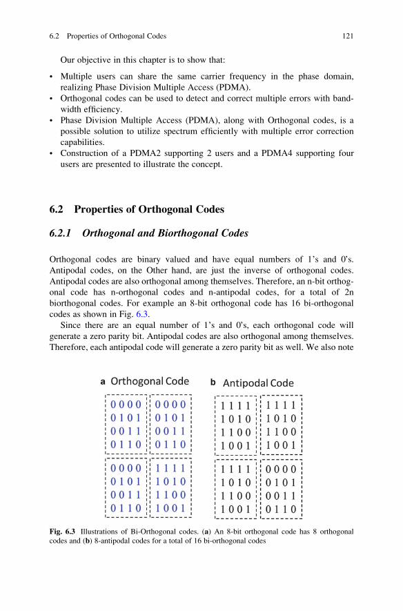
Our objective in this chapter is to show that:
• Multiple users can share the same carrier frequency in the phase domain,
realizing Phase Division Multiple Access (PDMA).
• Orthogonal codes can be used to detect and correct multiple errors with band-
width efficiency.
• Phase Division Multiple Access (PDMA), along with Orthogonal codes, is a
possible solution to utilize spectrum efficiently with multiple error correction
capabilities.
• Construction of a PDMA2 supporting 2 users and a PDMA4 supporting four
users are presented to illustrate the concept.
6.2 Properties of Orthogonal Codes
6.2.1 Orthogonal and Biorthogonal Codes
Orthogonal codes are binary valued and have equal numbers of 1’s and 0’s.
Antipodal codes, on the Other hand, are just the inverse of orthogonal codes.
Antipodal codes are also orthogonal among themselves. Therefore, an n-bit orthog-
onal code has n-orthogonal codes and n-antipodal codes, for a total of 2n
biorthogonal codes. For example an 8-bit orthogonal code has 16 bi-orthogonal
codes as shown in Fig. 6.3.
Since there are an equal number of 1’s and 0’s, each orthogonal code will
generate a zero parity bit. Antipodal codes are also orthogonal among themselves.
Therefore, each antipodal code will generate a zero parity bit as well. We also note
Fig. 6.3 Illustrations of Bi-Orthogonal codes. (a) An 8-bit orthogonal code has 8 orthogonal
codes and (b) 8-antipodal codes for a total of 16 bi-orthogonal codes
6.2 Properties of Orthogonal Codes 121
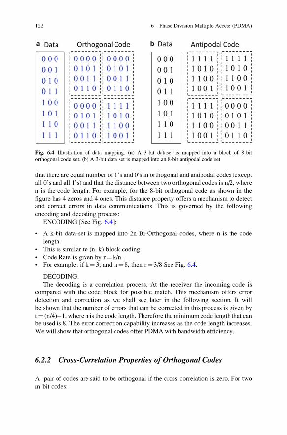
that there are equal number of 1’s and 0’s in orthogonal and antipodal codes (except
all 0’s and all 1’s) and that the distance between two orthogonal codes is n/2, where
n is the code length. For example, for the 8-bit orthogonal code as shown in the
figure has 4 zeros and 4 ones. This distance property offers a mechanism to detect
and correct errors in data communications. This is governed by the following
encoding and decoding process:
ENCODING [See Fig. 6.4]:
• A k-bit data-set is mapped into 2n Bi-Orthogonal codes, where n is the code
length.
• This is similar to (n, k) block coding.
• Code Rate is given by r¼ k/n.
• For example: if k¼ 3, and n¼ 8, then r¼ 3/8 See Fig. 6.4.
DECODING:
The decoding is a correlation process. At the receiver the incoming code is
compared with the code block for possible match. This mechanism offers error
detection and correction as we shall see later in the following section. It will
be shown that the number of errors that can be corrected in this process is given by
t¼ (n/4)�1, where n is the code length. Therefore the minimum code length that can
be used is 8. The error correction capability increases as the code length increases.
We will show that orthogonal codes offer PDMA with bandwidth efficiency.
6.2.2 Cross-Correlation Properties of Orthogonal Codes
A pair of codes are said to be orthogonal if the cross-correlation is zero. For two
m-bit codes:
Fig. 6.4 Illustration of data mapping. (a) A 3-bit dataset is mapped into a block of 8-bit
orthogonal code set. (b) A 3-bit data set is mapped into an 8-bit antipodal code set
122 6 Phase Division Multiple Access (PDMA)

• x1, x2, . . ., xm and
• y1, y2, . . ., ym,
The cross-correlation is given by the following equation:
Rxy 0ð Þ ¼Xmi¼1
xiyi ¼ 0 ð6:1Þ
It follows that an n-bit orthogonal code has n/2 1’s and n/2 0’s; i.e., there are n/2
positions where 1’s and 0’s differ [1–5]. Similarly, an n-bit antipodal code has n/2 1’s
and n/2 0’s; i.e., there are n/2 positions where 1’s and 0’s differ. Therefore, the distance
between two orthogonal codes is also n/2. For n¼ 8, these properties can be directly
verified fromFig. 6.1where the distance between any orthogonal code is 8/2¼ 4while
the distance between an orthogonal code and an antipodal code is 8. This distance
property can be used as a method of error control, as presented in the following
sections.
6.2.3 Error control Properties of Orthogonal Codes
An n-bit orthogonal code has n/2 1 s and n/2 0 s; i.e., there are n/2 positions where
1 s and 0 s differ. Therefore, the distance between two orthogonal codes is d¼ n/2.
This distance property can be used to detect an impaired received code by setting a
threshold midway between two orthogonal codes as shown in Fig. 6.5, where the
received coded is shown as a dotted line. This is given by:
dth ¼ n
4ð6:2Þ
Where n is the code length and dth is the threshold, which is midway between two
valid orthogonal codes. Therefore, for the given 8-bit orthogonal code, we have
Fig. 6.5 Illustration
of code correlation
6.2 Properties of Orthogonal Codes 123
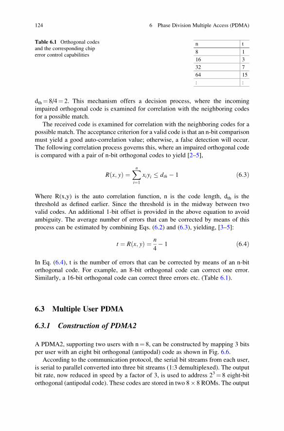
dth¼ 8/4¼ 2. This mechanism offers a decision process, where the incoming
impaired orthogonal code is examined for correlation with the neighboring codes
for a possible match.
The received code is examined for correlation with the neighboring codes for a
possible match. The acceptance criterion for a valid code is that an n-bit comparison
must yield a good auto-correlation value; otherwise, a false detection will occur.
The following correlation process governs this, where an impaired orthogonal code
is compared with a pair of n-bit orthogonal codes to yield [2–5],
R x; yð Þ ¼Xni¼1
xiyi � dth � 1 ð6:3Þ
Where R(x,y) is the auto correlation function, n is the code length, dth is the
threshold as defined earlier. Since the threshold is in the midway between two
valid codes. An additional 1-bit offset is provided in the above equation to avoid
ambiguity. The average number of errors that can be corrected by means of this
process can be estimated by combining Eqs. (6.2) and (6.3), yielding, [3–5]:
t ¼ R x; yð Þ ¼ n
4� 1 ð6:4Þ
In Eq. (6.4), t is the number of errors that can be corrected by means of an n-bit
orthogonal code. For example, an 8-bit orthogonal code can correct one error.
Similarly, a 16-bit orthogonal code can correct three errors etc. (Table 6.1).
6.3 Multiple User PDMA
6.3.1 Construction of PDMA2
A PDMA2, supporting two users with n¼ 8, can be constructed by mapping 3 bits
per user with an eight bit orthogonal (antipodal) code as shown in Fig. 6.6.
According to the communication protocol, the serial bit streams from each user,
is serial to parallel converted into three bit streams (1:3 demultiplexed). The output
bit rate, now reduced in speed by a factor of 3, is used to address 23¼ 8 eight-bit
orthogonal (antipodal code). These codes are stored in two 8� 8 ROMs. The output
Table 6.1 Orthogonal codes
and the corresponding chip
error control capabilities
n t
8 1
16 3
32 7
64 15
: :
124 6 Phase Division Multiple Access (PDMA)

of each ROM is a unique eight-bit orthogonal code, which is then modulated by a
QPSK modulator and transmitted through a channel, where the modulated wave-
form is in orthogonal space.
In the QPSK signal constellation, there are four symbols; each symbol represents
two code bits, one bit per code. Therefore QPSK can support 2 users (N¼ 2) as
shown below:
N ¼ Log 4ð ÞLog 2ð Þ ¼ 2 ð6:5Þ
Since there are two orthogonal waveforms, the number of errors (t) that can be
corrected is given by t¼ 2 [(n/4)�1]¼ 2, where n¼ 8 is the code length.
Fig. 6.6 Construction of PDMA2 based on QPSK modulator with n¼ 8. There are four phases or
four symbols, Each symbol represents two code bits, one from each code. Therefore, a QPSK
modulator can support two users
6.3 Multiple User PDMA 125
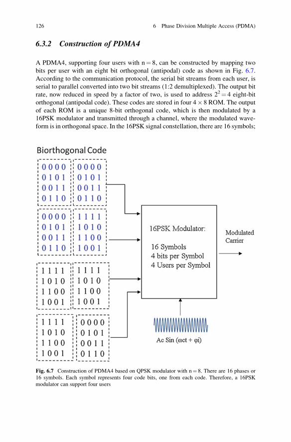
6.3.2 Construction of PDMA4
A PDMA4, supporting four users with n¼ 8, can be constructed by mapping two
bits per user with an eight bit orthogonal (antipodal) code as shown in Fig. 6.7.
According to the communication protocol, the serial bit streams from each user, is
serial to parallel converted into two bit streams (1:2 demultiplexed). The output bit
rate, now reduced in speed by a factor of two, is used to address 22¼ 4 eight-bit
orthogonal (antipodal code). These codes are stored in four 4� 8 ROM. The output
of each ROM is a unique 8-bit orthogonal code, which is then modulated by a
16PSK modulator and transmitted through a channel, where the modulated wave-
form is in orthogonal space. In the 16PSK signal constellation, there are 16 symbols;
Fig. 6.7 Construction of PDMA4 based on QPSK modulator with n¼ 8. There are 16 phases or
16 symbols. Each symbol represents four code bits, one from each code. Therefore, a 16PSK
modulator can support four users
126 6 Phase Division Multiple Access (PDMA)
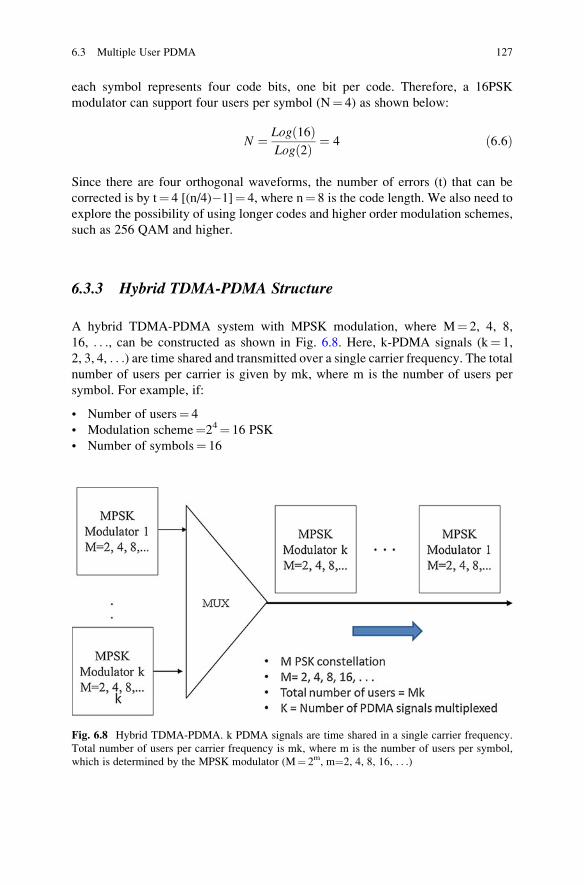
each symbol represents four code bits, one bit per code. Therefore, a 16PSK
modulator can support four users per symbol (N¼ 4) as shown below:
N ¼ Log 16ð ÞLog 2ð Þ ¼ 4 ð6:6Þ
Since there are four orthogonal waveforms, the number of errors (t) that can be
corrected is by t¼ 4 [(n/4)�1]¼ 4, where n¼ 8 is the code length. We also need to
explore the possibility of using longer codes and higher order modulation schemes,
such as 256 QAM and higher.
6.3.3 Hybrid TDMA-PDMA Structure
A hybrid TDMA-PDMA system with MPSK modulation, where M¼ 2, 4, 8,
16, . . ., can be constructed as shown in Fig. 6.8. Here, k-PDMA signals (k¼ 1,
2, 3, 4, . . .) are time shared and transmitted over a single carrier frequency. The total
number of users per carrier is given by mk, where m is the number of users per
symbol. For example, if:
• Number of users¼ 4
• Modulation scheme¼24¼ 16 PSK
• Number of symbols¼ 16
Fig. 6.8 Hybrid TDMA-PDMA. k PDMA signals are time shared in a single carrier frequency.
Total number of users per carrier frequency is mk, where m is the number of users per symbol,
which is determined by the MPSK modulator (M¼ 2m, m¼2, 4, 8, 16, . . .)
6.3 Multiple User PDMA 127

• Each symbol supports 4 users. 1 bit at a time
• Total number of users¼ 4 k
6.4 Ber Performance Analysis
We have established that an n-bit orthogonal code can correct t errors where
t¼ (n/4)�1. A measure of coding gain is then obtained by comparing the uncoded
word error WERU, to the coded word WERC. We examine this by means of the
following analytical means [6]:
With B PSK modulation, the Uncoded BER is given by:
BERU ¼ 0:5Exp 1� Eb=2 Noð Þ ð6:7Þ
The probability that the uncoded k-bit word (WERU) will be received in error is
1 minus the product of the probabilities that each bit will be received correctly.
Thus, we write:
WERU ¼ 1� 1� BERUð Þk ð6:8Þ
Since n> k, the coded bit energy to noise ratio will be modified to Ec/No.
Where
Ec/No(dB)¼Eb/No(dB) + 10log(k/n). Therefore, the coded BERc will be:
BERc ¼ 0:5Exp �Ec=2Noð Þ ð6:9Þ
The corresponding coded word error rate is:
WERC ¼Xnk¼tþ1
nk
� �BERK
C 1� BERCð Þn�k ð6:10Þ
When BERc< 0.5, the first term in the summation is the dominant one; therefore,
Eq. (6.5) can be simplified as
WERC � nk
� �BERk
c 1� BERcð Þn�k ð6:11Þ
Using n¼ 8, 16 and 64, we obtain the coded and the uncoded WER as shown in
Fig. 6.9. Coding gain is the difference in Eb/No between the uncoded and the coded
word error. Notice that at least 3–4 dB coding gain is available in this example.
128 6 Phase Division Multiple Access (PDMA)
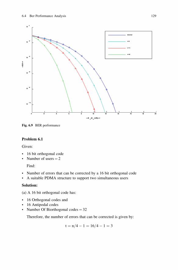
Problem 6.1
Given:
• 16 bit orthogonal code
• Number of users¼ 2
Find:
• Number of errors that can be corrected by a 16 bit orthogonal code
• A suitable PDMA structure to support two simultaneous users
Solution:
(a) A 16 bit orthogonal code has:
• 16 Orthogonal codes and
• 16 Antipodal codes
• Number Of Biorthogonal codes¼ 32
Therefore, the number of errors that can be corrected is given by:
t ¼ n=4� 1 ¼ 16=4� 1 ¼ 3
Fig. 6.9 BER performance
6.4 Ber Performance Analysis 129

(b) Since there are two users and we have 16 orthogonal codes and 16 antipodal
codes, we can assign 16 orthogonal codes to user 1 and 16 antipodal codes to user
2. See figure below. The circuit can be designed as follows:
• The incoming data from each user is serial to parallel converted into four parallel
streams. These four parallel bit streams are the address bit of the 4:16 decoder.
Therefore, depending on the address bit, one of 16 outputs of each decoder is
enabled to address the 16� 16 ROM.
• The output of each ROM is a unique 16 bit orthogonal or antipodal code. These
pair of codes is then used to modulate the QPSK modulator, having four symbols
(four phases), two bits per symbol, one bit from each user.
• Therefore, there are two users/symbol
Problem 6.2
Consider the previous problem again and construct a suitable PDMA structure
to support four users.
Solution:Since there are four users and we have 16 orthogonal codes and 16 antipodal codes,
we can assign 16 orthogonal codes to two users and 16 antipodal codes to two users.
See figure below for illustrations. The circuit can be designed as follows:
• The incoming data from each user is serial to parallel converted into three
parallel streams. These three parallel bit streams are the address bit of the 3:8
decoder. Therefore, depending on the address bit, one of eight outputs of each
decoder is enabled to address the 8� 16 ROM.
• The output of each ROM is a unique 16 bit orthogonal or antipodal code. These
four output codes are then used to modulate the 16PSK modulator, having
16 symbols (16 phases), 4 bits per symbol, 1 bit from each user.
• Therefore, there are four users/symbol
130 6 Phase Division Multiple Access (PDMA)
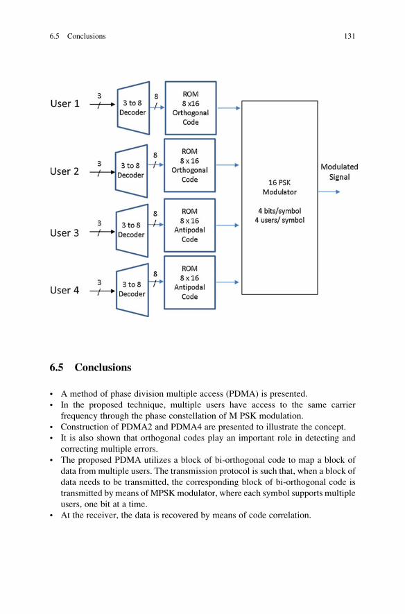
6.5 Conclusions
• A method of phase division multiple access (PDMA) is presented.
• In the proposed technique, multiple users have access to the same carrier
frequency through the phase constellation of M PSK modulation.
• Construction of PDMA2 and PDMA4 are presented to illustrate the concept.
• It is also shown that orthogonal codes play an important role in detecting and
correcting multiple errors.
• The proposed PDMA utilizes a block of bi-orthogonal code to map a block of
data from multiple users. The transmission protocol is such that, when a block of
data needs to be transmitted, the corresponding block of bi-orthogonal code is
transmitted by means of MPSKmodulator, where each symbol supports multiple
users, one bit at a time.
• At the receiver, the data is recovered by means of code correlation.
6.5 Conclusions 131

• We have examined the distance properties of orthogonal codes and have shown
that orthogonal codes can be used to detect and correct errors with bandwidth
efficiency.
• A hybrid-TDMA-PDMA scheme is also developed to improve spectrum usage.
• We have also presented BER Performance of PDMA.
References
1. B. Sklar, Digital Communications Fundamentals and Applications (Prentice Hall, Englewood
Cliffs, 1988)
2. S. Faruque, Battlefield wideband transceivers based on combined N-ary orthogonal signaling
and M-ary PSK modulation, SPIE Proceedings, Vol. 3709 Digitization of the Battle Space 1 V,
pp. 123–128, (1999)
3. S. Faruque, et al., Broadband wireless access based on code division parallel access, US Patent
No. 6208615, March 27, (2001)
4. S. Faruque, et al., Bi-orthogonal code division multiple access system, US Patent No. 6198719,
(March 6, 2001)
5. S. Faruque, Code division multiple access cable modem, US Patent No. 6647059, (November
2003)
6. G. Ungerboeck, Channel coding with multilevel/multiphase signals. IEEE Trans. Inf. Theory
28, 55–67 (1982)
132 6 Phase Division Multiple Access (PDMA)

Appendix A
Fourier Series
Fourier series is a mathematical function that applies to periodic signals. It states
that, a continuous time periodic signal contains an infinite number of harmonically
related sinusoidal waveforms. Fourier showed that, if the function f(t) is periodic,
then it can be represented by an infinite series as given below:
f tð Þ ¼ a02þ a1 cos ω0tð Þ þ a2 cos 2ω0tð Þ þ . . .
þ b1 sin ω0tð Þ þ b2 sin 2ω0tð Þ þ . . .ðA:1Þ
Or more conveniently as:
f tð Þ ¼ a02þX/n¼1
an cos nω0tð Þ þ �bn sin
�nω0t
� �� � ðA:2Þ
Here,
ω0 ¼ 2π f ¼ 2π=T
The Objective is to Determine Fourier Coefficients: a’s and b’s. Here is the
step-by-step process:
© Springer International Publishing Switzerland 2015
S. Faruque, Radio Frequency Source Coding Made Easy, SpringerBriefsin Electrical and Computer Engineering, DOI 10.1007/978-3-319-15609-5
133
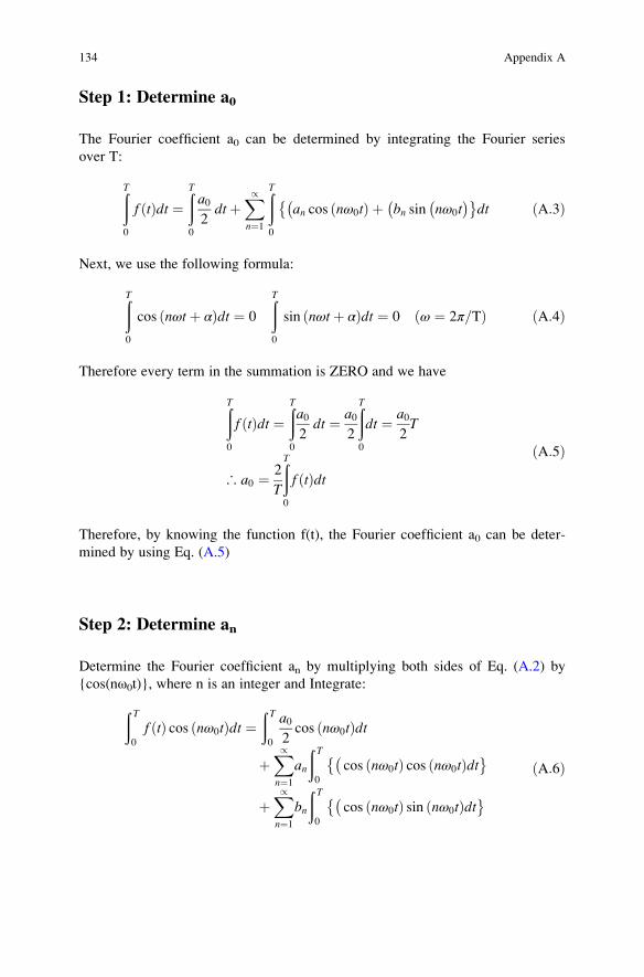
Step 1: Determine a0
The Fourier coefficient a0 can be determined by integrating the Fourier series
over T:
ðT
0
f tð Þdt ¼ðT
0
a02dtþ
X/n¼1
ðT
0
an cos nω0tð Þ þ �bn sin
�nω0t
� �� �dt ðA:3Þ
Next, we use the following formula:
ðT
0
cos nωtþ αð Þdt ¼ 0
ðT
0
sin nωtþ αð Þdt ¼ 0 ω ¼ 2π=Tð Þ ðA:4Þ
Therefore every term in the summation is ZERO and we have
ðT
0
f tð Þdt ¼ðT
0
a02dt ¼ a0
2
ðT
0
dt ¼ a02T
∴ a0 ¼ 2
T
ðT
0
f tð ÞdtðA:5Þ
Therefore, by knowing the function f(t), the Fourier coefficient a0 can be deter-
mined by using Eq. (A.5)
Step 2: Determine an
Determine the Fourier coefficient an by multiplying both sides of Eq. (A.2) by
{cos(nω0t)}, where n is an integer and Integrate:
ð T
0
f tð Þ cos nω0tð Þdt ¼ð T
0
a02cos nω0tð Þdt
þX/n¼1
an
ð T
0
�cos nω0tð Þ cos nω0tð Þdt� �
þX/n¼1
bn
ð T
0
�cos nω0tð Þ sin nω0tð Þdt� �
ðA:6Þ
134 Appendix A
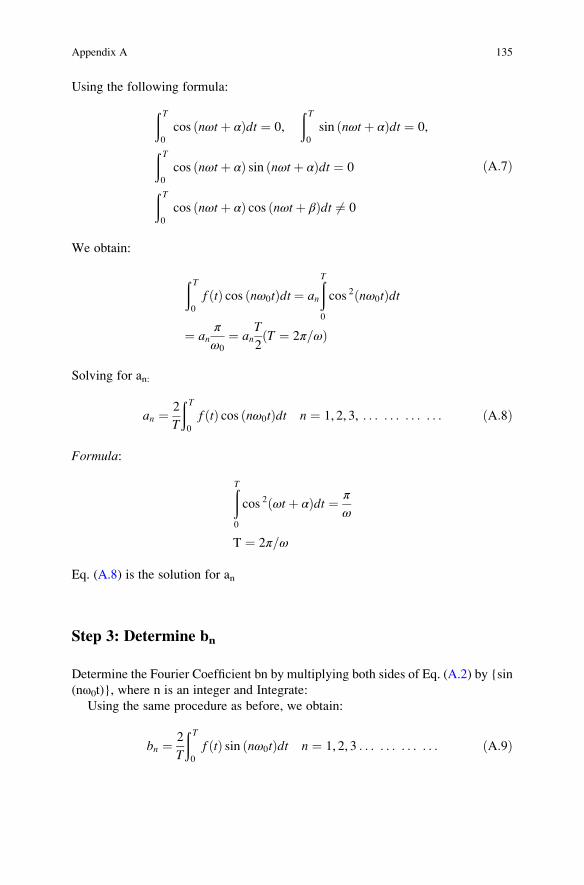
Using the following formula:
ð T
0
cos nωtþ αð Þdt ¼ 0,
ð T
0
sin nωtþ αð Þdt ¼ 0,
ð T
0
cos nωtþ αð Þ sin nωtþ αð Þdt ¼ 0
ð T
0
cos nωtþ αð Þ cos nωtþ βð Þdt 6¼ 0
ðA:7Þ
We obtain:
ð T
0
f tð Þ cos nω0tð Þdt ¼ an
ðT
0
cos 2 nω0tð Þdt
¼ anπ
ω0
¼ anT
2T ¼ 2π=ωð Þ
Solving for an:
an ¼ 2
T
ð T
0
f tð Þ cos nω0tð Þdt n ¼ 1, 2, 3, . . . . . . . . . . . . ðA:8Þ
Formula:
ðT
0
cos 2 ωtþ αð Þdt ¼ π
ω
T ¼ 2π=ω
Eq. (A.8) is the solution for an
Step 3: Determine bn
Determine the Fourier Coefficient bn by multiplying both sides of Eq. (A.2) by {sin
(nω0t)}, where n is an integer and Integrate:
Using the same procedure as before, we obtain:
bn ¼ 2
T
ð T
0
f tð Þ sin nω0tð Þdt n ¼ 1, 2, 3 . . . . . . . . . . . . ðA:9Þ
Appendix A 135

Formula:
ðT
0
sin 2 ωtþ αð Þdt ¼ π
ω
T ¼ 2π=ω
Eq. (A.9) is the solution for bn
Step 4: Substitute the Coefficients
Substitute the Fourier coefficients into the Fourier series given below:
f tð Þ ¼ a02þX/n¼1
�an cos nω0tð Þ þ �
bn sin nω0tð Þ� �
Summary
The Fourier series is given by:
f tð Þ ¼ a02þX/n¼1
�an cos nω0tð Þ þ �
bn sin nω0tð Þ� �
Fourier coefficients are given by:
a0 ¼ 2
T
ðT
0
f tð Þdt
an ¼ 2
T
ðT
0
f tð Þ cos nω0tð Þdt n ¼ 1, 2, 3, . . .
bn ¼ 2
T
ðT
0
f tð Þ sin nω0tð Þdt n ¼ 1, 2, 3, . . .
136 Appendix A

Guidelines to Find Fourier Spectrum
• Determine the Coefficient
a0 ¼ 2
T
ðT
0
f tð Þdt
an ¼ 2
T
ðT
0
f tð Þ cos nω0tð Þdt
bn ¼ 2
T
ðT
0
f tð Þ sin nω0tð Þdt
n ¼ 1, 2, 3, . . .
• Substitute the coefficient into the Fourier Series
f tð Þ ¼ a02þX/n¼1
�an cos nω0tð Þ þ �
bn sin nω0tð Þ� �
Problem: Square Wave
Given:
f tð Þ ¼ V 0 < t < 1
¼ �V 1 < t < 2
f tð Þ ¼ f tþ 2ð Þ
Find the Fourier series
Solution to Problem-1
Appendix A 137
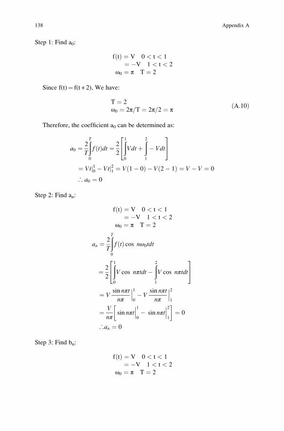
Step 1: Find a0:
f tð Þ ¼ V 0 < t < 1
¼ �V 1 < t < 2
ω0 ¼ π T ¼ 2
Since f(t)¼ f(t + 2), We have:
T ¼ 2
ω0 ¼ 2π=T ¼ 2π=2 ¼ π ðA:10Þ
Therefore, the coefficient a0 can be determined as:
a0 ¼ 2
T
ðT
0
f tð Þdt ¼ 2
2
ð1
0
Vdtþð2
1
� Vdt
24
35
¼ Vtj10 � Vtj21 ¼ V 1� 0ð Þ � V 2� 1ð Þ ¼ V � V ¼ 0
∴ a0 ¼ 0
Step 2: Find an:
f tð Þ ¼ V 0 < t < 1
¼ �V 1 < t < 2
ω0 ¼ π T ¼ 2
an ¼ 2
T
ðT
0
f tð Þ cos nω0tdt
¼ 2
2
ð1
0
V cos nπtdt�ð2
1
V cos nπtdt
24
35
¼ Vsin nπt
nπ
���10� V
sin nπt
nπ
���21
¼ V
nπsin nπt
���10� sin nπt
���21
� �¼ 0
∴an ¼ 0
Step 3: Find bn:
f tð Þ ¼ V 0 < t < 1
¼ �V 1 < t < 2
ω0 ¼ π T ¼ 2
138 Appendix A

bn ¼ 2
T
ðT
0
f tð Þ sin nω0tdt
¼ 2
2
ð1
0
V sin nπtdt�ð2
1
V sin nπtdt
24
35
¼ �Vcos nπt
nπ
���10þ V
cos nπt
nπ
���21
¼ � V
nπcos nπt
���10� cos nπt
���21
� �
bn ¼ � V
nπcos nπ � 1ð Þ � cos 2nπ � cos nπð Þ½ �
¼ � 4
nπ2 cos nπ � cos 2nπ � 1½ � ¼ 4V
nπn ¼ 1, 3, . . .ð Þ
¼ 0 n ¼ 2, 4, . . . :ð Þ
∴bn ¼ 4V
nπ
Step 4: Substitute a0, an and bn into the Fourier series f(t):
f tð Þ ¼ a02þX/n¼1
�an cos nω0tð Þ þ �
bn sin nω0tð Þ� �
¼ 0þX/n¼1
0þ 4V
nπsign nω0tð Þ
¼ 4V
nπ
X/n¼1
1
nsign nω0tð Þ n ¼ 1, 3, 5, . . . . . . . . .ZX
Appendix A 139

Appendix B
Fourier Transform
Fourier transform is a mathematical function that applies to non-periodic signals. It
states that, a discrete time non-periodic signal contains an infinite number of
harmonically related sinusoidal waveforms. Fourier showed that, if the function f
(t) is non-periodic, then it can be represented in two ways:
• Time domain representation:
V tð Þ ¼ V < 0 < t < T
¼ 0 elsewhere
• Frequency domain representation: “Fourier Transform”
V ωð Þ ¼ðT
0
V � e� jωtdt
The above frequency domain expression can be expanded to obtain an infinite
number of harmonically related sinusoidal waveform as follows:
© Springer International Publishing Switzerland 2015
S. Faruque, Radio Frequency Source Coding Made Easy, SpringerBriefsin Electrical and Computer Engineering, DOI 10.1007/978-3-319-15609-5
141
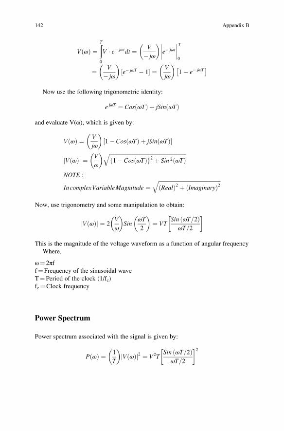
V ωð Þ ¼ðT
0
V � e� jωtdt ¼ V
� jω
e� jωt
��������T
0
¼ V
� jω
e� jωT � 1½ � ¼ V
jω
1� e� jωT� �
Now use the following trigonometric identity:
e jωT ¼ Cos ωTð Þ þ jSin ωTð Þ
and evaluate V(ω), which is given by:
V ωð Þ ¼ V
jω
1� Cos ωTð Þ þ jSin ωTð Þ½ �
V ωð Þj j ¼ V
ω
ffiffiffiffiffiffiffiffiffiffiffiffiffiffiffiffiffiffiffiffiffiffiffiffiffiffiffiffiffiffiffiffiffiffiffiffiffiffiffiffiffiffiffiffiffiffiffiffiffiffiffiffiffiffiffiffiffi1� Cos ωTð Þf g2 þ Sin 2 ωTð Þ
q
NOTE :
IncomplexVariableMagnitude ¼ffiffiffiffiffiffiffiffiffiffiffiffiffiffiffiffiffiffiffiffiffiffiffiffiffiffiffiffiffiffiffiffiffiffiffiffiffiffiffiffiffiffiffiffiffiffiRealð Þ2 þ Imaginaryð Þ2
q
Now, use trigonometry and some manipulation to obtain:
V ωð Þj j ¼ 2V
ω
Sin
ωT
2
¼ VT
Sin ωT=2ð ÞωT=2
� �
This is the magnitude of the voltage waveform as a function of angular frequency
Where,
ω¼ 2πff¼ Frequency of the sinusoidal wave
T¼ Period of the clock (1/fc)
fc¼Clock frequency
Power Spectrum
Power spectrum associated with the signal is given by:
P ωð Þ ¼ 1
T
V ωð Þj j2 ¼ V2T
Sin ωT=2ð ÞωT=2
� �2
142 Appendix B

where
V ωð Þj j ¼ VTSin ωT=2ð Þ
ωT=2
� �
Where,
• V(t)¼Voltage, which is a function of time
• T¼ Period
The power spectrum has an infinite number of harmonically related components
General Expression for Two Sided Response
A more general equation (Two Sided) is:
V ωð Þ ¼ð/
�/V tð Þ � e� jωtdt
In this case, V(ω) is called two sided spectrum of V(t). This is due to both positive
and negative frequencies used in the integral. The function can be a voltage or a
current.
Appendix B 143
Related Documents