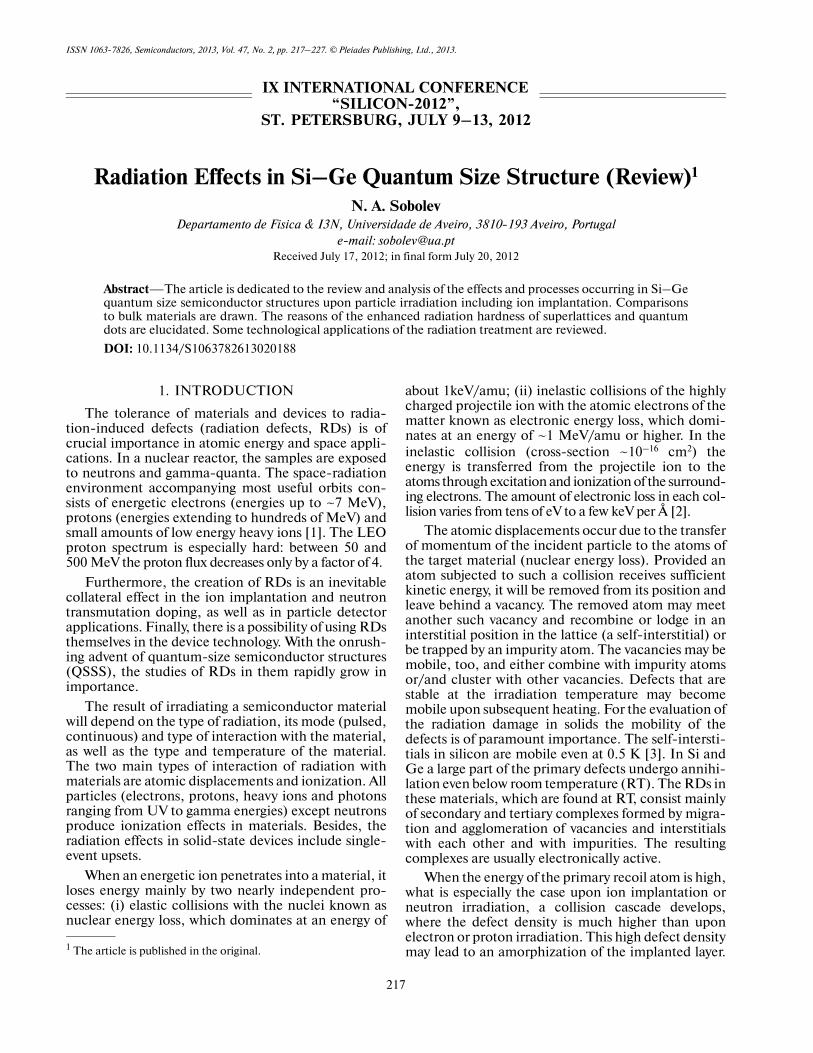
ISSN 10637826, Semiconductors, 2013, Vol. 47, No. 2, pp. 217–227. © Pleiades Publishing, Ltd., 2013. 217 1. INTRODUCTION The tolerance of materials and devices to radia tioninduced defects (radiation defects, RDs) is of crucial importance in atomic energy and space appli cations. In a nuclear reactor, the samples are exposed to neutrons and gammaquanta. The spaceradiation environment accompanying most useful orbits con sists of energetic electrons (energies up to ~7 MeV), protons (energies extending to hundreds of MeV) and small amounts of low energy heavy ions [1]. The LEO proton spectrum is especially hard: between 50 and 500 MeV the proton flux decreases only by a factor of 4. Furthermore, the creation of RDs is an inevitable collateral effect in the ion implantation and neutron transmutation doping, as well as in particle detector applications. Finally, there is a possibility of using RDs themselves in the device technology. With the onrush ing advent of quantumsize semiconductor structures (QSSS), the studies of RDs in them rapidly grow in importance. The result of irradiating a semiconductor material will depend on the type of radiation, its mode (pulsed, continuous) and type of interaction with the material, as well as the type and temperature of the material. The two main types of interaction of radiation with materials are atomic displacements and ionization. All particles (electrons, protons, heavy ions and photons ranging from UV to gamma energies) except neutrons produce ionization effects in materials. Besides, the radiation effects in solidstate devices include single event upsets. When an energetic ion penetrates into a material, it loses energy mainly by two nearly independent pro cesses: (i) elastic collisions with the nuclei known as nuclear energy loss, which dominates at an energy of about 1keV/amu; (ii) inelastic collisions of the highly charged projectile ion with the atomic electrons of the matter known as electronic energy loss, which domi nates at an energy of ~1 MeV/amu or higher. In the inelastic collision (crosssection ~10 –16 cm 2 ) the energy is transferred from the projectile ion to the atoms through excitation and ionization of the surround ing electrons. The amount of electronic loss in each col lision varies from tens of eV to a few keV per Å [2]. The atomic displacements occur due to the transfer of momentum of the incident particle to the atoms of the target material (nuclear energy loss). Provided an atom subjected to such a collision receives sufficient kinetic energy, it will be removed from its position and leave behind a vacancy. The removed atom may meet another such vacancy and recombine or lodge in an interstitial position in the lattice (a selfinterstitial) or be trapped by an impurity atom. The vacancies may be mobile, too, and either combine with impurity atoms or/and cluster with other vacancies. Defects that are stable at the irradiation temperature may become mobile upon subsequent heating. For the evaluation of the radiation damage in solids the mobility of the defects is of paramount importance. The selfintersti tials in silicon are mobile even at 0.5 K [3]. In Si and Ge a large part of the primary defects undergo annihi lation even below room temperature (RT). The RDs in these materials, which are found at RT, consist mainly of secondary and tertiary complexes formed by migra tion and agglomeration of vacancies and interstitials with each other and with impurities. The resulting complexes are usually electronically active. When the energy of the primary recoil atom is high, what is especially the case upon ion implantation or neutron irradiation, a collision cascade develops, where the defect density is much higher than upon electron or proton irradiation. This high defect density may lead to an amorphization of the implanted layer. Radiation Effects in Si–Ge Quantum Size Structure (Review) 1 N. A. Sobolev Departamento de Fisica & I3N, Universidade de Aveiro, 3810193 Aveiro, Portugal email: [email protected] Received July 17, 2012; in final form July 20, 2012 Abstract—The article is dedicated to the review and analysis of the effects and processes occurring in Si–Ge quantum size semiconductor structures upon particle irradiation including ion implantation. Comparisons to bulk materials are drawn. The reasons of the enhanced radiation hardness of superlattices and quantum dots are elucidated. Some technological applications of the radiation treatment are reviewed. DOI: 10.1134/S1063782613020188 IX INTERNATIONAL CONFERENCE “SILICON2012”, ST. PETERSBURG, JULY 9–13, 2012 1 The article is published in the original.

Welcome message from author
This document is posted to help you gain knowledge. Please leave a comment to let me know what you think about it! Share it to your friends and learn new things together.
Transcript
ISSN 1063�7826, Semiconductors, 2013, Vol. 47, No. 2, pp. 217–227. © Pleiades Publishing, Ltd., 2013.
217
1. INTRODUCTION
The tolerance of materials and devices to radia�tion�induced defects (radiation defects, RDs) is ofcrucial importance in atomic energy and space appli�cations. In a nuclear reactor, the samples are exposedto neutrons and gamma�quanta. The space�radiationenvironment accompanying most useful orbits con�sists of energetic electrons (energies up to ~7 MeV),protons (energies extending to hundreds of MeV) andsmall amounts of low energy heavy ions [1]. The LEOproton spectrum is especially hard: between 50 and500 MeV the proton flux decreases only by a factor of 4.
Furthermore, the creation of RDs is an inevitablecollateral effect in the ion implantation and neutrontransmutation doping, as well as in particle detectorapplications. Finally, there is a possibility of using RDsthemselves in the device technology. With the onrush�ing advent of quantum�size semiconductor structures(QSSS), the studies of RDs in them rapidly grow inimportance.
The result of irradiating a semiconductor materialwill depend on the type of radiation, its mode (pulsed,continuous) and type of interaction with the material,as well as the type and temperature of the material.The two main types of interaction of radiation withmaterials are atomic displacements and ionization. Allparticles (electrons, protons, heavy ions and photonsranging from UV to gamma energies) except neutronsproduce ionization effects in materials. Besides, theradiation effects in solid�state devices include single�event upsets.
When an energetic ion penetrates into a material, itloses energy mainly by two nearly independent pro�cesses: (i) elastic collisions with the nuclei known asnuclear energy loss, which dominates at an energy of
about 1keV/amu; (ii) inelastic collisions of the highlycharged projectile ion with the atomic electrons of thematter known as electronic energy loss, which domi�nates at an energy of ~1 MeV/amu or higher. In theinelastic collision (cross�section ~10–16 cm2) theenergy is transferred from the projectile ion to theatoms through excitation and ionization of the surround�ing electrons. The amount of electronic loss in each col�lision varies from tens of eV to a few keV per Å [2].
The atomic displacements occur due to the transferof momentum of the incident particle to the atoms ofthe target material (nuclear energy loss). Provided anatom subjected to such a collision receives sufficientkinetic energy, it will be removed from its position andleave behind a vacancy. The removed atom may meetanother such vacancy and recombine or lodge in aninterstitial position in the lattice (a self�interstitial) orbe trapped by an impurity atom. The vacancies may bemobile, too, and either combine with impurity atomsor/and cluster with other vacancies. Defects that arestable at the irradiation temperature may becomemobile upon subsequent heating. For the evaluation ofthe radiation damage in solids the mobility of thedefects is of paramount importance. The self�intersti�tials in silicon are mobile even at 0.5 K [3]. In Si andGe a large part of the primary defects undergo annihi�lation even below room temperature (RT). The RDs inthese materials, which are found at RT, consist mainlyof secondary and tertiary complexes formed by migra�tion and agglomeration of vacancies and interstitialswith each other and with impurities. The resultingcomplexes are usually electronically active.
When the energy of the primary recoil atom is high,what is especially the case upon ion implantation orneutron irradiation, a collision cascade develops,where the defect density is much higher than uponelectron or proton irradiation. This high defect densitymay lead to an amorphization of the implanted layer.
Radiation Effects in Si–Ge Quantum Size Structure (Review)1
N. A. SobolevDepartamento de Fisica & I3N, Universidade de Aveiro, 3810�193 Aveiro, Portugal
e�mail: [email protected] July 17, 2012; in final form July 20, 2012
Abstract—The article is dedicated to the review and analysis of the effects and processes occurring in Si–Gequantum size semiconductor structures upon particle irradiation including ion implantation. Comparisonsto bulk materials are drawn. The reasons of the enhanced radiation hardness of superlattices and quantumdots are elucidated. Some technological applications of the radiation treatment are reviewed.
DOI: 10.1134/S1063782613020188
IX INTERNATIONAL CONFERENCE “SILICON�2012”,
ST. PETERSBURG, JULY 9–13, 2012
1 The article is published in the original.
218
SEMICONDUCTORS Vol. 47 No. 2 2013
SOBOLEV
The accompanying defect rearrangement processesare usually quite complex and not yet understood in alldetails even in elemental semiconductors such as Siand Ge.
The total cross�section for the displacement of anatom from its regular lattice site as a result of an elasticcollision is given by [4]
(1)
where E is the kinetic energy of the incident particle,T is the kinetic energy transmitted to the lattice atom,dσ(E, T) is the differential cross section of the corre�sponding interaction. The integration is performedover the energy T from the minimum energy Td neces�sary for the displacement of a lattice atom into aninterstitial position to the maximum energy Tm whichthe incident particle can transmit to the target atom.The energy Td is called threshold energy. The differen�tial cross section depends on the interaction potential.In the case of charged particles (electrons, protons,ions) the interaction can be described by the Coulomb
σ E( ) dσ E T,( ),
Td
Tm
∫=
potential; for the neutral particles (neutrons) it israther similar to the collision of hard spheres. Theexperimental values of Td for silicon and germaniumare equal to 21 eV and 27.5 eV, respectively [4]. To cal�culate the number of displacements produced by anincident particle, one has to solve the integral inEq. (1), taking into account the type of interaction.
Collisions with neutrons are much harder in termsof the average energy transmitted to a target atom thanthose with protons of equal energy. The energy of elec�trons must achieve hundreds of keV in order to imple�ment transfer of an energy amount exceeding Td. Onthe contrary, in the case of the ions, the masses of theincident particle and the target atom are comparable,so that the energy transfer is very efficient, and even inthe case of the ion etching of the surface with energiesof hundreds of eV the creation of RDs must be takeninto account. Fast neutron irradiation produces ener�getic recoil atoms and in terms of the produced dam�age can be understood as “internal” self�ion implanta�tion. However, due to the small collision cross�sec�tion, the displacement cascades are well separated inthe crystal volume even at moderate irradiation doses.
On the contrary, implantation of medium andheavy mass ions produces a very dense damage withina thin subsurface layer of a solid target, so that amor�phization of this layer can be readily achieved. Thecritical fluence needed for the amorphization of agiven crystal depends on the ion mass and the targettemperature. For each ion�target combination, thereis a critical temperature above which the amorphiza�tion becomes impossible due to dynamical defectannealing [5,6]. (At cryogenic temperatures, theamorphization of silicon was induced even under MeVelectron irradiation, but the required fluences wereexceedingly high [7, 8].) The energy dependence ofthe critical ion fluence exists but is less pronounced.The theoretical description of the crystalline�to�amorphous transition upon ion irradiation is still amatter of debate [9]. Another important peculiarity ofthe ion irradiation is the sputtering of the target [10].
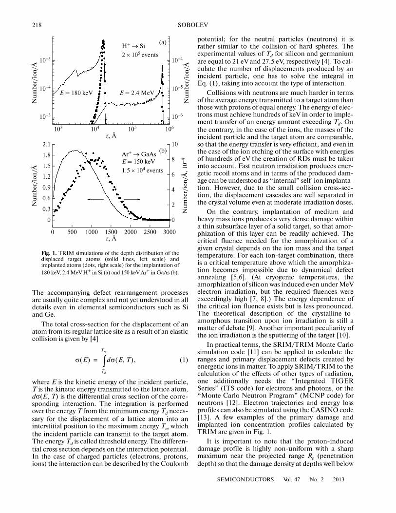
In practical terms, the SRIM/TRIM Monte Carlosimulation code [11] can be applied to calculate theranges and primary displacement defects created byenergetic ions in matter. To apply SRIM/TRIM to thecalculation of the effects of other types of radiation,one additionally needs the “Integrated TIGERSeries” (ITS code) for electrons and photons, or the“Monte Carlo Neutron Program” (MCNP code) forneutrons [12]. Electron trajectories and energy lossprofiles can also be simulated using the CASINO code[13]. A few examples of the primary damage andimplanted ion concentration profiles calculated byTRIM are given in Fig. 1.
It is important to note that the proton�induceddamage profile is highly non�uniform with a sharpmaximum near the projected range Rp (penetrationdepth) so that the damage density at depths well below
2.1
0
1.8
1.5
1.2
0.9
0.6
0.3
0
500 1000 1500 2000 2500 3000z, Å
10
8
6
4
2
0
(b)
Nu
mbe
r/io
n/Å
Nu
mbe
r/io
n/Å
, 10
−4
Ar+ → GaAsE = 150 keV
1.5 × 10⁴ events
10−5
106
z, Å
(a)N
um
ber/
ion
/Å
Nu
mbe
r/io
n/Å
H+ → Si
2 × 10⁵ events
E = 180 keV E = 2.4 MeV
105104103
10−4
10−3
10−4
10−5
10−6
Fig. 1. TRIM simulations of the depth distribution of thedisplaced target atoms (solid lines, left scale) andimplanted atoms (dots, right scale) for the implantation of180 keV, 2.4 MeV H+ in Si (a) and 150 keV Ar+ in GaAs (b).
SEMICONDUCTORS Vol. 47 No. 2 2013
RADIATION EFFECTS IN Si–Ge QUANTUM SIZE STRUCTURE (REVIEW) 219
Rp can decrease with increasing proton energy, despitethe increase of the total energy deposited in elastic col�lisions (see Fig. 1). This fact must be taken intoaccount when irradiating nanometer thick layers con�taining, e.g., quantum dots or a quantum well and sit�uated near the sample surface.
The effect of ionization on the defect production inthe common semiconductors exists but mostly is aminor one. Anyway, the ionization (formation of elec�tron�hole pairs) alone does not produce RDs in thesesemiconductors as it is the case in wide�gap insulators.However, the degradation of a MOS device, especiallyat low irradiation doses, is almost entirely due to thelong�lived effects of ionization in the dielectric subele�ment, i.e. in the gate insulator [14]. In bipolar devicesthe primary effect of ionizing radiation is gain reduction.This is usually due to an increase in surface recombina�tion near the emitter�base region. Ionization damagealso causes leakage current to increase [15].
The sensitivity of the device parameters to irradia�tion is further determined by material properties, suchas the threshold energy for atomic displacement (seeabove), probability of the annihilation of the self�interstitials and vacancies, type and level of doping,position of the defect�induced energy levels in the gap.There is a comprehensive literature on the subject ofthe radiation hardness of semiconductors and semi�conductor devices [16].
Summarizing, in order to predict the radiationdamage in QSSS, first of all one needs knowledge onthe creation, transformation, and annihilation pro�cesses of RDs in corresponding bulk materials includ�ing alloys. Whereas these processes in Si are wellunderstood, the information concerning Ge is muchless detailed. The worst situation is to be stated for theSiGe alloys. To solve the problem of the radiationhardness of a device, one has to establish which layer(or layers) in a concrete, probably very complicated,structure predominantly determines the deviceparameters degradation. In devices containing low�dimensional active layers, it is important to knowwhich is the volume sampled by the wavefunction ofthe electrons and holes confined in the layers. Finally,the role of the Fermi level, heterointerfaces and strainin the defect evolution and defect reactions, themutual influence of the adjacent layers, and theimpact of the quantum confinement on the structureand properties of local defects, which are supposed tobe already known from the studies of the correspond�ing bulk semiconductors, have to be elucidated.
On the other hand, what is the useful informationwe can learn from the irradiation studies?
—Influence of the defects on the electronic prop�erties of QSSS and on the corresponding deviceparameters;
—elucidation of the electronic structure of QSSSas well as of the carrier transport, relaxation and
recombination processes in them using defects asmicroprobes;
—diffusion processes in QSSS;—novel technological processes of micro�, nano�
and optoelectronics.The review presents a survey of effects occurring in
SiGe quantum wells (QWs), superlattices (SLs) andquantum dots (QDs) upon electron and proton irradi�ation as well as upon ion implantation. Sec. 2 is dedi�cated to the important issue of the radiation hardness.It is shown that QD�based devices can withstandmuch higher radiation fluences than corresponding2D and bulk structures. The physical mechanisms ofthis phenomenon are discussed. In Sec. 3, peculiari�ties of the amorphization of SLs upon ion implanta�tion are considered. Sec. 4 demonstrates examples ofthe application of particle irradiation to the devicetechnology. At the end, concise conclusions aredrawn.
2. RADIATION HARDNESS OF QUANTUM SIZE HETEROSTRUCTURES
2.1. General Remarks
The term “radiation hardness” (the same as “radi�ation resistance”) describes the ability of a structure’sproperty to withstand the deteriorating action of radi�ation. The recombination parameters of semiconduc�tors are much more sensitive to RDs than e.g. equilib�rium carrier concentration or mobility. RDs with deeplevels in the bandgap act as non�radiative recombina�tion centers (lifetime killers) limiting the photolumi�nescence (PL) and electroluminescence (EL) inten�sity as well as photosensitivity.
The increased tolerance of defects is one of themost important promises of the self�assembled QDnanotechnology [17]. The basic argument is that morestrongly localized carriers exhibit reduced migrationto non�radiative centers. As pointed out in Ref. [18],Turnbull was probably the first to propose, as early as1950, that small crystals will contain fewer defects[19]. This “self�purification” was shown [18] to be anintrinsic property of defects in semiconductor nanoc�rystals, for the formation energies of defects increaseas the size of the nanocrystal decreases. This result hasbeen severely criticized [20], nonetheless, we shall seethat a very similar effect is obviously observed in irra�diated QDs. Importantly, only relatively small dots canbe defect�free. So, e.g., when the QDs exceed certaindimensions, dislocations are observed within the dots.
The influence of Ge doping on the accumulationprocess of radiation defects in silicon irradiated withgamma�rays and elementary particles has been thesubject of numerous investigations (for an early reviewsee, e.g., Ref. [21]). The influence of irradiation on theSiGe�based diodes and MOSFETS is also a subject ofintense research (see, e.g., Refs. [22–25]). For quite along time there had been only one RD containing a Ge
220
SEMICONDUCTORS Vol. 47 No. 2 2013
SOBOLEV
atom, namely the Ge�vacancy (Ge–V) pair [26, 27],that has been positively identified. However, it annealswell below room temperature. It has been suggestedthat at irradiation temperatures Ti ≥ 300 K the Geatoms act as centers of indirect recombination ofFrenkel pair components [28–30]. The further progresshas been limited to the detection of the Ge�divacancypair (Ge–V2)[31, 32].
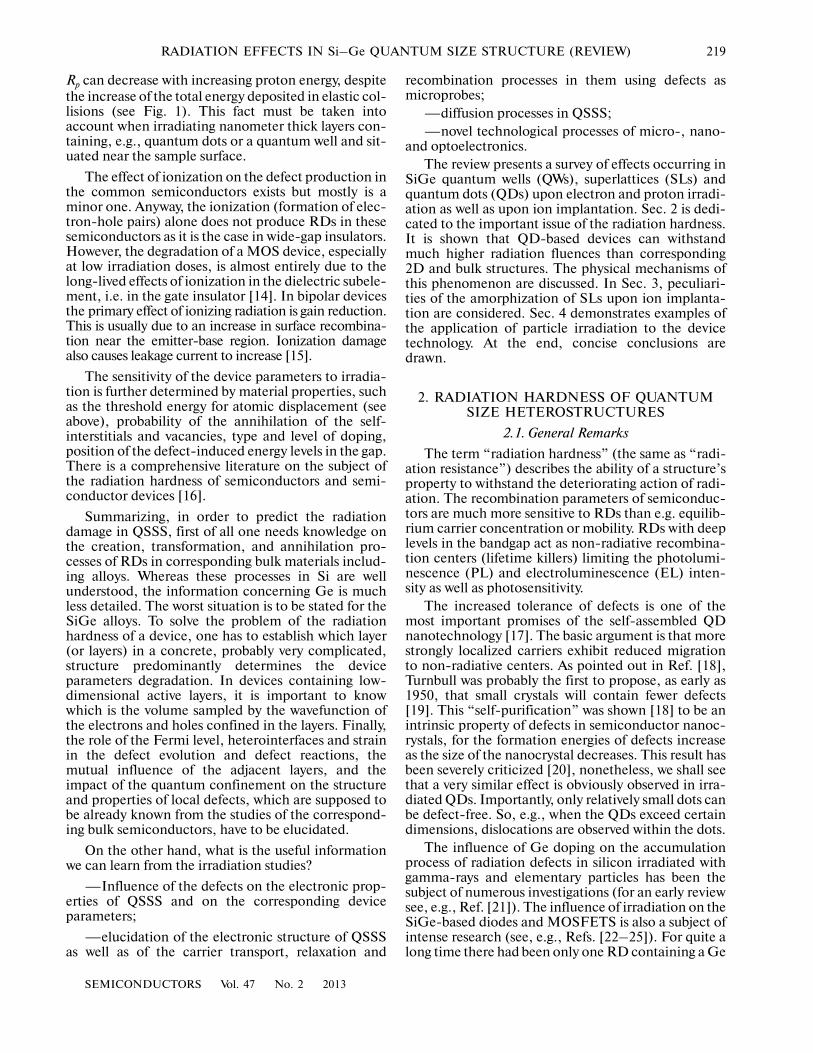
The influence of the Ge content on the propertiesof a few point defects known for pure Si has beenunderstood [33–39]. An example is given in Fig. 2. Theconclusions drawn from these studies with respect tothe defect level position in the gap are as follows [40, 41]:
(i) The observed level displacement towards thevalence band with increasing Ge is characteristic of(almost) all defect levels.
(ii) Those levels which cross the midgap levelchange from being an electron trap in the upper half ofthe band gap to becoming a hole trap in the lower halfof the band gap. This is clearly the case for the single�acceptor levels of the E�center (a substitutional donor�neighboring vacancy complex).
(iii) None of these levels are pinned to any of theband edges.
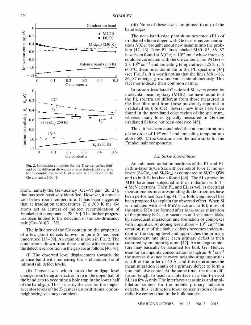
The near�band�edge photolumunescence (PL) ofirradiated silicon doped with Ge in various concentra�tions N(Ge) brought about new insights into the prob�lem [42, 43]. New PL lines labeled M80–83, 86, 87have been found at N(Ge) � 1019 cm–3 whose intensitycould be correlated with the Ge content. For N(Ge) =2 × 1020 cm–3 and annealing temperatures 525 ≥ Ta ≥600°C these lines dominate in the PL spectrum [44](see Fig. 3). It is worth noting that the lines M81–83,86, 87 emerge, grow and vanish simultaneously. Thisfact may indicate their common nature.
In proton�irradiated Ge�doped Si layers grown bymolecular�beam epitaxy (MBE), we have found thatthe PL spectra are different from those measured inGe�free films and from those previously reported inirradiated bulk Si(Ge). Several new lines have beenfound in the near�band edge region of the spectrum,whereas many lines typically measured in Ge�freeirradiated Si have not been observed [45].
Thus, it has been concluded that at concentrationsof the order of 1020 cm–3 and annealing temperaturesabove 500°C the Ge atoms are the main sinks for theFrenkel pair components.
2.2. Si/Ge Superlattices
An enhanced radiation hardness of the PL and ELin thin�layer Si/Ge SLs with periods of 10 or 15 mono�layers (Si6Ge4 and Si9Ge6) as compared to Si/Ge QWsand to bulk Si has been found [46]. The SLs grown byMBE have been subjected to the irradiation with 3–4 MeV electrons. Then PL and EL as well as electricalmeasurements on corresponding diode structures havebeen performed (see Fig. 4). The following model hasbeen proposed to explain the observed effect. When Siis irradiated with 3–4 MeV electrons at RT, most ofthe stable RDs are formed after long�range migrationof the primary RDs, i. e. vacancies and self�interstitials,by subsequent interaction and formation of complexeswith impurities. At doping levels above ~ 1017 cm–3 thecreation rate of the stable defects becomes indepen�dent of the doping level and approaches the primarydisplacement rate since each primary defect is thencaptured by an impurity atom [47]. An analogous pic�ture may basically be assumed for bulk Ge. Hence,even for an impurity concentration as high as 1019 cm–3
the average distance between neighbouring impuritiesis still of the order of 40 Å, and this determines themean migration length of a primary defect to form anon�radiative center. At the same time, the mean dif�fusion length to reach an interface in a short�periodSL is a few Å only. The interfaces act as sinks and anni�hilation centers for the mobile primary radiationdefects, thus leading to a lower concentration of non�radiative centers than in the bulk material.
0
0
0.2
0.4
0.6
0.8
1.0
1.20.1 0.2 0.3 0.4 0.5
Ion
izat
ion
en
thal
py,
Ec −
Et,
eV
Ge content x
Ecν(250 K)
(1/2)Ecν(250 K)
V20/+
V2=/−
V2−/0
V2−/0
0
0
−0.2
−0.4
−0.6
−0.8
−1.0
−1.20.1 0.2 0.3 0.4 0.5
Ion
izat
ion
en
thal
py,
eV
Ge content x
Valence band (230 K)
Conduction band
MCTSDLTS
Midgap (230 K)
Fig. 2. Ionization enthalpies for the E�center defect (left)and of the different divacancy charge states (right) relativeto the conduction band Ec of silicon as a function of theGe content x [40, 41].
SEMICONDUCTORS Vol. 47 No. 2 2013
RADIATION EFFECTS IN Si–Ge QUANTUM SIZE STRUCTURE (REVIEW) 221
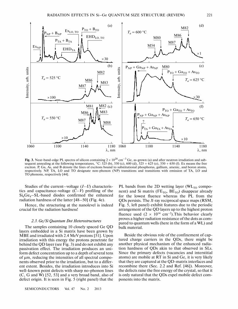
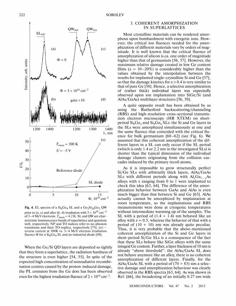
Studies of the current–voltage (I–U) characteris�tics and capacitance�voltage (C–V) profiling of theSi6Ge4–SL�based diodes confirmed the enhancedradiation hardness of the latter [48–50] (Fig. 4e).
Hence, the structuring at the nanolevel is indeedcrucial for the radiation hardness!
2.3. Ge/Si Quantum Dot Heterostructures
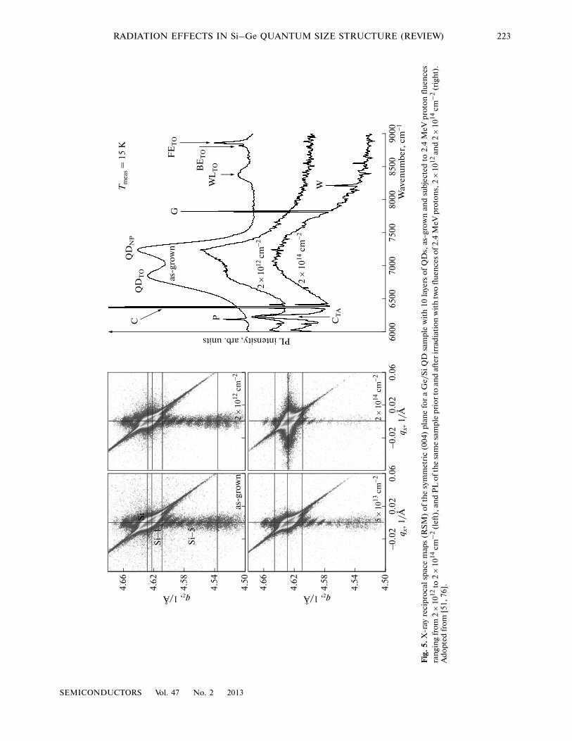
The samples containing 10 closely spaced Ge QDlayers embedded in a Si matrix have been grown byMBE and irradiated with 2.4 MeV protons [51]. Uponirradiation with this energy the protons penetrate farbehind the QD layer (see Fig. 3) and do not exhibit anypassivation effect. The irradiation produces an uni�form defect concentration up to a depth of several tensof μm, reducing the intensities of all spectral compo�nents observed prior to the irradiation, but to a differ�ent extent. Besides, the irradiation introduces into Siwell�known point defects with sharp no�phonon lines(C, G and W) [52, 53] and a very broad band, also ofdefect origin. It is seen in Fig. 5 (right panel) that the
PL bands from the 2D wetting layer (WLTO compo�nent) and Si matrix (FETO, BETO) disappear alreadyfor the lowest fluence whereas the PL from theQDs persists. The X�ray reciprocal space maps (RSM,Fig. 5, left panel) exhibit features due to the periodicarrangement of the QD layers up to the highest protonfluence used (2 × 1014 cm–2).This behavior clearlyproves a higher radiation resistance of the dots as com�pared to quantum wells (here in the form of a WL) andbulk material.
Beside the obvious role of the confinement of cap�tured charge carriers in the QDs, there might beanother physical mechanism of the enhanced radia�tion hardness of QDs akin to that observed in SLs.Since the primary defects (vacancies and interstitialatoms) are mobile at RT in Si and Ge, it is very likelythat they are captured at the QD�matrix interfaces andrecombine there (Sec. 2.2 and Ref. [46]). Moreover,the defects raise the free energy of the crystal, so that itis only natural that the QDs expel mobile defect com�ponents into the matrix.
1060 1100 1140 1180λ, nm
(a)In
ten
sity
, ar
b. u
nit
s (b)
(c)
PNP + BNP
PTA + BTA
EHDTAExNP
ExLO, TO
EHDLO, TO
PTO + BTO
×30
×100
~~
Ta = 525 °C
M82
M83M86
M87
M81 M82
M83
M88M87
M86
×10
Ta = 550 °C
1060 1100 1140 1180λ, nm
(d)
Inte
nsi
ty,
arb.
un
its (e)
(f)
×1
×30
~~
Ta = 625 °C
×10
Ta = 650 °C
PTO + GaTO + AsTO
PNP + GaNP + AsNP
PTA + GaTA + AsTA
?
M80
PTO + GaTO + AsTO
PNP + GaNP + AsNP
Ta = 600 °C
M80
M82
M86
M87M54
Fig. 3. Near�band�edge PL spectra of silicon containing 2 × 1020 cm–3 Ge, as�grown (a) and after neutron irradiation and sub�sequent annealing at the following temperatures, °C: 525 (b), 550 (c), 600 (d), 525 + 625 (e), 550 + 650 (f). Ex means the freeexciton. P, Ga, As, and B denote the lines of excitons bound to substitutional phosphorus, gallium, arsenic, and boron atoms,respectively. NP, TA, LO and TO designate non�phonon (NP) transitions and transitions with emission of TA, LO andTO phonons, respectively [44].
222
SEMICONDUCTORS Vol. 47 No. 2 2013
SOBOLEV
When the Ge/Si QD layers are deposited so tightlythat they form a superlattice, the radiation hardness ofthe structure is even higher [54, 55]. In spite of theexpected high concentration of nonradiative recombi�nation centres caused by the proton�induced damage,the PL emission from the Ge dots has been observedeven for the highest irradiation fluence of 2 × 1014 cm–2.
3. COHERENT AMORPHIZATION IN SUPERLATTICES
Most crystalline materials can be rendered amor�phous upon bombardment with energetic ions. How�ever, the critical ion fluences needed for the amor�phization of different materials vary by orders of mag�nitude. It is well known that the critical fluence ofamorphization of silicon is ca. one order of magnitudehigher than that of germanium [56, 57]. However, themaximum relative damage created in low Ge contentfilms (x = 10–20%) is considerably higher than thevalues obtained by the interpolation between theresults for implanted single�crystalline Si and Ge [57],so that the damage kinetics for x > 0.4 is very similar tothat of pure Ge [58]. Hence, a selective amorphizationof (rather thick) individual layers was expectedlyobserved upon ion implantation into SiGe/Si (andAlAs/GaAs) multilayer structures [56, 59].
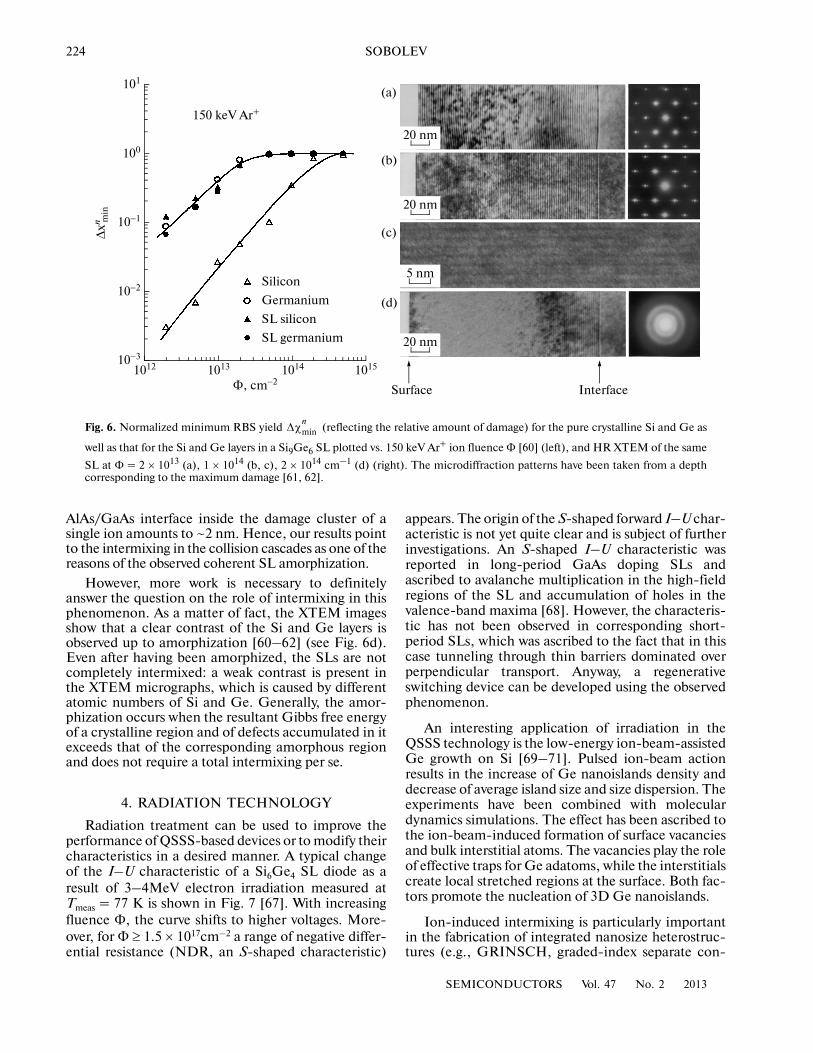
A quite opposite result has been obtained by ususing the Rutherford backscattering/channeling(RBS) and high�resolution cross�sectional transmis�sion electron microscopy (HR XTEM) on short�period Si6Ge4 and Si9Ge6 SLs: the Si and Ge layers inthe SLs were amorphized simultaneously at one andthe same fluence that coincided with the critical flu�ence for bulk germanium [60–62] (see Fig. 6). Weassumed that this coherent amorphization of the dif�ferent layers in a SL can only occur if the SL period(which is only 1.4 or 2.2 nm in the investigated SLs) isshorter than the typical dimension of the individualdamage clusters originating from the collision cas�cades induced by the primary recoil atoms.
As it is impossible to grow structurally perfectSi/Ge SLs with arbitrarily thick layers, AlAs/GaAsSLs with different periods along with AlxGa1 – xAsalloys with x ranging from 0 to 1 were implanted tocheck this idea [63, 64]. The difference of the amor�phization behavior between GaAs and AlAs is evenmuch bigger than that between Si and Ge [65]. AlAsactually cannot be amorphized by implantation atroom temperature, so the implantations and RBSmeasurements were done at cryogenic temperatureswithout intermediate warming up of the samples. TheSL with a period of (1.4 + 1.4) nm behaved like analloy with x = 0.5, whereas the behavior of that with aperiod of (10 + 10) nm was already quite peculiar.Thus, it is very probable that the above�mentionedcoherent amorphization of the Si and Ge layers inshort�period Si/Ge SLs is a consequence of the factthat these SLs behave like SiGe alloys with the sameintegral Ge content. Further, a layer thickness of 10 nm isalready “above threshold”: the AlAs/GaAs SL doesnot behave anymore like an alloy, there is no coherentamorphization of different layers. Finally, for theAlAs/GaAs SL with a period of (70 + 83) nm a selec�tive damage and amorphization behaviour was clearlyobserved in the RBS spectra [63, 64]. As was shown inRef. [66], the broadening of an initially 0.27 nm wide
0
50 10 15Φ, 1016 cm−2
10
20
30
40
50
I/I 0
Tmeas = 300 K
U = −5 V
Reference diode
SL diode
(e)
1200 1400 1200 1300 1400λ, nm
(d)(b)
Inte
nsi
ty,
arb.
un
its
Φ = 5 × 1016 cm−2
gain ×10
(a) (c)
Φ = 0
QWTOQWNPSLNP
Fig. 4. EL spectra of a Si6Ge4 SL and a Ge2Si20Ge2 QW
prior to (a, c) and after (b, d) irradiation with 5 × 1016 cm–2
of 3–4 MeV electrons. Tmeas = 4.2 K. SL and QW are char�acteristic luminescence bands of superlattice and quantumwell, respectively. NP and TO indices refer to no�phonontransitions and their TO�replica, respectively [75]. (e)—reverse current at 300K vs. 3–4 MeV electron irradiationfluence Φ for a Si6Ge4 SL and an industrial diode [49].
SEMICONDUCTORS Vol. 47 No. 2 2013
RADIATION EFFECTS IN Si–Ge QUANTUM SIZE STRUCTURE (REVIEW) 223
4.50
−0.
020.
020.
06q x
, 1/
Å
4.54
4.58
4.62
4.66
qz, 1/Å
5 ×
1013
cm
−2
−0.
020.
020.
06q x
, 1/
Å
2 ×
1014
cm
−2
4.50
4.54
4.58
4.62
4.66
qz, 1/Å
as�g
row
n2 ×
1012
cm
−2
Si
Si−
5
Si−
1
6000
PL intensity, arb. units65
0070
0075
0080
0085
0090
00W
aven
um
ber,
cm
−1
W
G
C P CT
A
QD
TO
QD
NP
FE
TO
BE
TO
WL
TO
as�g
row
n
2 ×
1012
cm
−2
2 ×
1014
cm
−2
Tm
eas =
15
K
Fig
. 5.
X�r
ay r
ecip
roca
l sp
ace
map
s (R
SM
) of
th
e sy
mm
etri
c (0
04)
plan
e fo
r a
Ge/
Si
QD
sam
ple
wit
h 1
0 la
yers
of
QD
s, a
s�gr
own
an
d su
bjec
ted
to 2
.4 M
eV p
roto
n f
luen
ces
ran
gin
g fr
om 2
× 1
012 to
2 ×
1014
cm
–2 (
left
), a
nd
PL
of t
he
sam
e sa
mpl
e pr
ior
to a
nd
afte
r ir
radi
atio
n w
ith
two
flue
nce
s of
2.4
MeV
pro
ton
s, 2
× 1
012 a
nd
2 ×
1014
cm
–2 (
righ
t).
Ado
pted
from
[51
, 76]
.
224
SEMICONDUCTORS Vol. 47 No. 2 2013
SOBOLEV
AlAs/GaAs interface inside the damage cluster of asingle ion amounts to ~2 nm. Hence, our results pointto the intermixing in the collision cascades as one of thereasons of the observed coherent SL amorphization.
However, more work is necessary to definitelyanswer the question on the role of intermixing in thisphenomenon. As a matter of fact, the XTEM imagesshow that a clear contrast of the Si and Ge layers isobserved up to amorphization [60–62] (see Fig. 6d).Even after having been amorphized, the SLs are notcompletely intermixed: a weak contrast is present inthe XTEM micrographs, which is caused by differentatomic numbers of Si and Ge. Generally, the amor�phization occurs when the resultant Gibbs free energyof a crystalline region and of defects accumulated in itexceeds that of the corresponding amorphous regionand does not require a total intermixing per se.
4. RADIATION TECHNOLOGY
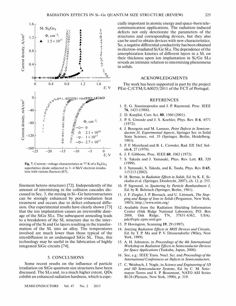
Radiation treatment can be used to improve theperformance of QSSS�based devices or to modify theircharacteristics in a desired manner. A typical changeof the I–U characteristic of a Si6Ge4 SL diode as aresult of 3–4MeV electron irradiation measured atTmeas = 77 K is shown in Fig. 7 [67]. With increasingfluence Φ, the curve shifts to higher voltages. More�over, for Φ ≥ 1.5 × 1017cm–2 a range of negative differ�ential resistance (NDR, an S�shaped characteristic)
appears. The origin of the S�shaped forward I–U char�acteristic is not yet quite clear and is subject of furtherinvestigations. An S�shaped I–U characteristic wasreported in long�period GaAs doping SLs andascribed to avalanche multiplication in the high�fieldregions of the SL and accumulation of holes in thevalence�band maxima [68]. However, the characteris�tic has not been observed in corresponding short�period SLs, which was ascribed to the fact that in thiscase tunneling through thin barriers dominated overperpendicular transport. Anyway, a regenerativeswitching device can be developed using the observedphenomenon.
An interesting application of irradiation in theQSSS technology is the low�energy ion�beam�assistedGe growth on Si [69–71]. Pulsed ion�beam actionresults in the increase of Ge nanoislands density anddecrease of average island size and size dispersion. Theexperiments have been combined with moleculardynamics simulations. The effect has been ascribed tothe ion�beam�induced formation of surface vacanciesand bulk interstitial atoms. The vacancies play the roleof effective traps for Ge adatoms, while the interstitialscreate local stretched regions at the surface. Both fac�tors promote the nucleation of 3D Ge nanoislands.
Ion�induced intermixing is particularly importantin the fabrication of integrated nanosize heterostruc�tures (e.g., GRINSCH, graded�index separate con�
10−1
10151012 1013 1014
Φ, cm−2
10−3
10−2
100
101
Silicon
Germanium
SL silicon
SL germanium
Δxn m
in
Surface Interface
(a)
(b)
(c)
(d)
20 nm
20 nm
20 nm
5 nm
Fig. 6. Normalized minimum RBS yield (reflecting the relative amount of damage) for the pure crystalline Si and Ge as
well as that for the Si and Ge layers in a Si9Ge6 SL plotted vs. 150 keV Ar+ ion fluence Φ [60] (left), and HR XTEM of the same
SL at Φ = 2 × 10¹³ (a), 1 × 10¹⁴ (b, c), 2 × 1014 cm–1 (d) (right). The microdiffraction patterns have been taken from a depthcorresponding to the maximum damage [61, 62].
Δχminn
150 keV Ar+
SEMICONDUCTORS Vol. 47 No. 2 2013
RADIATION EFFECTS IN Si–Ge QUANTUM SIZE STRUCTURE (REVIEW) 225
finement hetero�structure) [72]. Independently of theamount of intermixing in the collision cascades dis�cussed in Sec. 3, the mixing in Si–Ge heterostructurescan be strongly enhanced by post�irradiation heattreatment and occurs due to defect�enhanced diffu�sion. Our experimental results have clearly shown [73]that the ion implantation causes an irreversible dam�age of the SiGe SLs. The subsequent annealing leadsto a breakdown of the SL structure due to the inter�mixing of the Si and Ge layers resulting in the transfor�mation of the SL into an alloy. The temperaturesinvolved are much lower than those typical of theinterdiffusion in an undamaged SiGe SL. Thus, thistechnology may be useful in the fabrication of highlyintegrated SiGe circuits [74].
5. CONCLUSIONS
Some recent results on the influence of particleirradiation on SiGe quantum size structures have beendiscussed. The SLs and, to a much higher extent, QDsexhibit an enhanced radiation hardness, which is espe�
cially important in atomic energy and space�born tele�communication applications. The radiation�induceddefects not only deteriorate the parameters of thestructures and corresponding devices, but they alsocan be used to obtain devices with new characteristics.So, a negative differential conductivity has been obtainedin electron�irradiated Si/Ge SLs. The dependence of theamorphization kinetics of different layers in a SL ontheir thickness upon ion implantation in Si/Ge SLsreveals an intimate relation to intermixing phenomenain solids.
ACKNOWLEDGMENTS
The work has been supported in part by the projectPEst�C/CTM/LA0025/2011 of the FCT of Portugal.
REFERENCES
1. E. G. Stassinopoulos and J. P. Raymond, Proc. IEEE76, 1423 (1988).
2. D. Kanjilal, Curr. Sci. 80, 1560 (2001).3. P. S. Gwozdz and J. S. Koehler, Phys. Rev. B 6, 4571
(1972).4. J. Bourgoin and M. Lannoo, Point Defects in Semicon�
ductors II, Experimental Aspects, Springer Ser. in SolidState Science, vol. 35 (Springer, Berlin, Heidelberg,1983).
5. F. F. Morehead and B. L. Crowder, Rad. Eff. Def. Sol�ids 6, 27 (1970).
6. J. F. Gibbons, Proc. IEEE 60, 1062 (1972).7. S. Takeda and J. Yamasaki, Phys. Rev. Lett. 83, 320
(1999).8. J. Yamasaki, S. Takeda, and K. Tsuda, Phys. Rev. B 65,
115213 (2002).9. H. Bernas, in Radiation Effects in Solids, Ed. by K. E. Si�
ckafus et al. (Springer, Dordrecht, 2007), ch. 12, p. 353.10. P. Sigmund, in Sputtering by Particle Bombardment I,
Ed. by R. Behrisch (Springer, Berlin, 1981).11. J. F. Ziegler, J. P. Biersack, and U. Littmark, The Stop�
ping and Range of Ions in Solids (Pergamon, New York,1985); http://www.srim.org/
12. Available from the Radiation Shielding InformationCenter (Oak Ridge National Laboratory, P.O. Box2008, Oak Ridge, TN, 37831�6362, USA)[email protected]
13. P. Hovington, Scanning 19, 29 (1997).14. Ionizing Radiation Effects in MOS Devices and Circuits,
Ed. by T. P. Ma and P. V. Dressendorfer (Wiley, NewYork, 1989).
15. A. H. Johnston, in Proceedings of the 4th InternationalWorkshop on Radiation Effects in Semiconductor Devicesfor Space Applications (Tsukuba, Japan, 2000).
16. See, e.g.: IEEE Trans. Nucl. Sci. and Proceedings of theInternational Conferences on Defects in Semiconductors.
17. C. Weisbuch, J. Nagle, in Science and Engineering of 1Dand 0D Semiconductor Systems, Ed. by C. M. Soto�mayor�Torres and S. P. Beaumont, NATO ASI SeriesB124 (Plenum, New York, 1990), p. 319.
−160−25 −20 −15 −10 −5 0
U, V
−120
−80
−40
0
Φ, cm−2:
02.1 × 10¹⁶
1 × 10¹⁷
2.7 × 10¹⁷
Cu
rren
t d
ensi
ty,
mA
/cm
2
0
0 0.4 0.8 1.2 1.6U, V
0.4
0.8
1.2
1.6
Φ, cm−2:
SL Si6Ge4
1.5 × 10¹⁷
Cu
rren
t d
ensi
ty,
A/c
m2
Fig. 7. Current–voltage characteristics at 77 K of a Si6Ge4superlattice diode subjected to 3–4 MeV electron irradia�tion with various fluences [67].
226
SEMICONDUCTORS Vol. 47 No. 2 2013
SOBOLEV
18. G. M. Dalpian and J. R. Chelikowsky, Phys. Rev. Lett.96, 226802 (2006).
19. D. Turnbull, J. Appl. Phys. 21, 1022 (1950).
20. M.�H. Du, S. C. Erwin, Al. L. Efros, and D. J. Norris,Phys. Rev. Lett. 100, 179702 (2008).
21. N. A. Sobolev, in Physics, Chemistry and Application ofNanostrucutres (World Scientific, Singapore, 1997),p. 43.
22. C. Claeys and E. Simoen, Radiation Effects in AdvancedSemiconductor Materials and Devices (Springer Verlag,New York, 2002).
23. H. Ohyama, T. Nagano, K. Takakura, M. Motoki,K. Matsuo, H. Nakamura, M. Sawada, S. Kuboyam,M. B. Gonzalez, E. Simoen, G. Eneman, and C. Claeys,Thin Solid Films 518, 2517 (2010).
24. H. Ohyama, N. Naka, K. Takakura, I. Tsunoda,M. B. Gonzalez, E. Simoen, and C. Claeys, Micro�electron. Eng. 88, 484 (2011).
25. H. Ohyama, K. Shigaki, K. Hayama, K. Takakura,M. Yoneoka, Y. Takami, J. Vanhellemont, E. Simoen,and C. Claeys, Res. Rep. Kumamoto�NCT 1, 93(2009).
26. G. D. Watkins, IEEE Trans. Nucl. Sci. 16, 13 (1969).
27. G. D. Watkins, J. R. Troxell, and A. P. Chatterjee, Inst.Phys. Conf. Ser. 46, 16 (1979).
28. L. I. Khirunenko, V. I. Shakhovtsov, and V. V. Shumov,Semiconductors 32, 120 (1998).
29. V. G. Golubev, V. V. Emtsev, P. M. Klinger, G. I. Kro�potov, and Y. V. Shamartsev, Sov. Phys. Semicond. 26,328 (1992).
30. M. S. Saidov, S. L. Lutpullaev, A. Yusupov, I. G. Ata�baev, L. I. Khirunenko, N. A. Matchanov, D. Saidov,and M. U. Hajiev, Phys. Solid State 49, 1658 (2007).
31. L. I. Khirunenko, Yu. V. Pomozov, M. G. Sosnin,M. O. Trypachko, A. V. Duvanskii, N. V. Abrosimov,H. Riemann, S. B. Lastovskii, L. I. Murin, V. P. Mar�kevich, and A. R. Peaker, Mater. Sci. Semicond. Pro�cess. 9, 525 (2006).
32. L. Khirunenko, Yu. Pomozov, M. Sosnin, N. Abrosi�mov, and W. Schröder, Physica B 308–310, 550 (2001).
33. L. I. Khirunenko, Yu. V. Pomozov, M. G. Sosnin,A. Duvanskii, V. J. B. Torres, J. Coutinho, R. Junes,P. R. Briddon, N. V. Abrosimov, and H. Riemann,Physica B 401–402, 200 (2007).
34. S. Hayama, G. Davies, J. Tan, V. P. Markevich,A. R. Peaker, J. Evans�Freeman, K. D. Vernon�Parry,and N. V. Abrosimov, Physica B 340–342, 823 (2003).
35. J. P. Leit o, A. Carvalho, J. Coutinho, R. N. Pereira,N. M. Santos, A. O. Ankiewicz, N. A. Sobolev, M. Bar�roso, J. Lundsgaard Hansen, A. Nylandsted Larsen,and P. R. Briddon, Phys. Rev. B 84, 165211 (2011).
36. A. Mesli, Vl. Kolkovsky, L. Dobaczewski, A. Nyland�sted Larsen, and N. V. Abrosimov, Nucl. Instrum.Methods Phys. Res. B 253, 154 (2006).
37. A. Mesli and A. Nylandsted Larsen, J. Phys.: Condens.Matter 17, S2171 (2005).
a
38. V. P. Markevich, A. R. Peaker, L. I. Murin, andN. V. Abrosimov, J. Phys.: Condens. Matter 15, S2835(2003).
39. A. R. Peaker and V. P. Markevich, in Silicon Hetero�structure Handbook: Materials, Fabrication, Devices,Circuits and Applications of SiGe and Si Strained�LayerEpitaxy, Ed. by J. D. Cressler (CRC Taylor Francis,2006), p. 107.
40. H. av Skardi, A. B. Hansen, A. Mesli, and A. N. Larsen,Nucl. Instrum. Methods Phys. Res. B 186, 195 (2002).
41. A. Nylandsted Larsen, A. Bro Hansen, and A. Mesli,Mater. Sci. Eng. B 154–155, 85 (2008).
42. A. V. Voevodova, F. P. Korshunov, N. A. Sobolev, andA. A. Stuk, Sov. Phys. Semicond. 23, 734 (1989).
43. A. V. Voevodova, F. P. Korshunov, N. A. Sobolev, andA. A. Stuk, in Defect Control in Semiconductors (Amster�dam, 1990), v. 1, p. 387.
44. N. A. Sobolev and M. H. Nazaré, Physica B 273–274,271 (1999).
45. A. O. Ankiewicz, N. A. Sobolev, J. P. Leit o, M. C. Car�mo, R. N. Pereira, J. Lundsgaard Hansen, andA. Nylandsted Larsen, Nucl. Instrum. Methods Phys.Res. B 248, 127 (2006).
46. N. A. Sobolev, F. P. Korshunov, R. Sauer, K. Thonke,U. König, and H. Presting, J. Cryst. Growth 167, 502(1996).
47. V. I. Gubskaya, P. V. Kuchinskii, and V. M. Lomako,Rad. Eff. Def. Solids 55, 35 (1981).
48. E. S. Basova, S. B. Lastovskii, N. A. Sobolev, F. P. Kor�shunov, U. König, and H. Presting, in Proceedings of the5th All�Russian and International Conference on TopicalProblems of Solid�State Electronics and Microelectronics(TRTU, Taganrog, 1998), p. 71.
49. E. S. Basova, S. B. Lastovskii, N. A. Sobolev, F. P. Kor�shunov, U. König, and H. Presting, in Proceedings of the8th International Conference on Radiation Physics ofSolids (Sevastopol, 1998).
50. N. A. Sobolev, E. S. Basova, S. B. Lastovskii, F. P. Kor�shunov, N. A. Poklonskii, A. I. Syaglo, M. H. Nazaré,H. Presting, and U. König, in Abstracts of the20th International Conference on Defects Semiconduc�tors (Berkeley, USA, 1999), p. 293.
51. N. A. Sobolev, A. Fonseca, J. P. Leit o, M. C. Carmo,H. Presting, and H. Kibbel, Phys. Status Solidi C 0,1267 (2003).
52. G. Davies, Phys. Rep. 176, 83 (1989).
53. R. Sauer, in Landolt–Börnstein (Springer, Berlin, 1989),vol. 22b, p. 338.
54. A. Fonseca, N. A. Sobolev, J. P. Leit o, E. Alves,M. C. Carmo, N. D. Zakharov, P. Werner, A. A. Tonkikh,and G. E. Cirlin, J. Luminesc. 121, 417 (2006).
55. J. P. Leit o, N. A. Sobolev, M. R. Correira, M. C. Carmo,N. Stepina, A. Yakimov, A. Nikiforov, S. Magalh es,and E. Alves, Thin Solid Films 517, 303 (2008).
56. D. J. Eaglesham, J. M. Poate, D. C. Jacobson, M. Ce�rullo, L. N. Pfeiffer, and K. West, Appl. Phys. Lett. 58,523 (1991).
a
a
a
aa
SEMICONDUCTORS Vol. 47 No. 2 2013
RADIATION EFFECTS IN Si–Ge QUANTUM SIZE STRUCTURE (REVIEW) 227
57. D. Y. C. Lie, A. Vantomme, F. Eisen, T. Vreeland, Jr.,M.�A. Nicolet, T. K. Carns, V. Arbet�Engels, andK. L. Wang, J. Appl. Phys. 74, 6039 (1993).
58. T. E. Haynes and O. W. Holland, Appl. Phys. Lett. 61,61 (1992).
59. M. Vos, C. Wu, I. V. Mitchell, T. E. Jackman, J.�M. Ba�ribeau, and J. McCaffrey, Appl. Phys. Lett. 58, 951(1991).
60. N. A. Sobolev, K. Gärtner, U. Kaiser, U. König,H. Presting, B. Weber, E. Wendler, and W. Wesch,Mater. Sci. Forum 248–249, 289 (1997).
61. N. A. Sobolev, U. Kaiser, I. I. Khodos, H. Presting, andU. König, in Mater. Res. Soc. Symposium Proceedings(Warrendale, PA, USA, 1999), vol. 540, p. 91.
62. N. A. Sobolev, U. Kaiser, I. I. Khodos, H. Presting, andU. König, Bull. Russ. Acad. Sci. Phys. 63, 1066 (1999).
63. N. A. Sobolev, M. C. Carmo, B. Breeger, E. Wendler,W. Wesch, R. Hey, and H. T. Grahn, in Abstracts of theInternational Conference on Electronic Mater. andEMRS Spring Meeting (Strasbourg, 2000).
64. N. A. Sobolev, M. V. Carmo, B. Breeger, E. Wendler,W. Wesch, R. Hey, and H. T. Grahn, in Abstracts of the15th International Conference on Ion Beam Analysis,IBA�15 (Cairns, 2001).
65. B. Breeger, E. Wendler, Ch. Schubert, and W. Wesch,Nucl. Instrum. Methods Phys. Res. B 148, 468 (1999).
66. M. Bode, A. Ourmazd, J. Cunningham, and M. Hong,Phys. Rev. Lett. 67, 843 (1991).
67. N. A. Sobolev, E. S. Basova, S. B. Lastovskii, F. P. Kor�shunov, N. A. Poklonskii, A. I. Syaglo, M. H. Nazaré,and H. Presting, U. König, in Proceedings of the2nd All�Russia Conference on Silicon�2000 (Moscow,2000) p. 107.
68. E. F. Schubert, J. E. Cunningham, and W. T. Tsang,Appl. Phys. Lett. 51, 817 (1987).
69. A. V. Dvurechenskii, J. V. Smagina, V. A. Zinovyev,S. A. Teys, and A. K. Gutakovskii, Int. J. Nanosci. 3, 19(2004).
70. N. P. Stepina, A. V. Dvurechenskii, V. A. Ambrister,J. V. Smagina, V. A. Volodin, A. V. Nenashev, J. P. Leit o,M. C. Carmo, and N. A. Sobolev, Thin Solid Films517, 309 (2008).
71. Zh. V. Smagina, P. L. Novikov, V. A. Zinovyev,V. A. Armbrister, S. A. Teys, and A. V. Dvurechenskii,J. Cryst. Growth 323, 244 (2011).
72. For a review of QW intermixing, see, e. g. IEEE J. Sel.Top. Quantum Electron. 4 (4) (1998).
73. N. A. Sobolev, J. Gerster, G. Mauckner, M. Wolpert,W. Limmer, K. Thonke, R. Sauer, H. Presting, andU. König, Nucl. Instrum. Methods Phys. Res. B 136–138, 1057 (1998).
74. D. J. Paul, Semicond. Sci. Technol. 19, R75 (2004).
75. N. A. Sobolev and H. Presting, unpublished.
76. M. A. L. Fonseca, PhD Thesis (Universidate de Aveiro,2007).
a
Related Documents