UV LED for Automotive EHS Guide for 3D Printing Controlling Coating Temperatures Racing Ahead with UV/EB Curing 2017 Quarter 1 Vol. 3, No. 1 Official Publication of RadTech International North America

Welcome message from author
This document is posted to help you gain knowledge. Please leave a comment to let me know what you think about it! Share it to your friends and learn new things together.
Transcript
UV LED for Automotive
EHS Guide for 3D Printing
Controlling Coating Temperatures
Racing Ahead with UV/EB Curing
2017 Quarter 1Vol. 3, No. 1
Official Publication of RadTech International North America
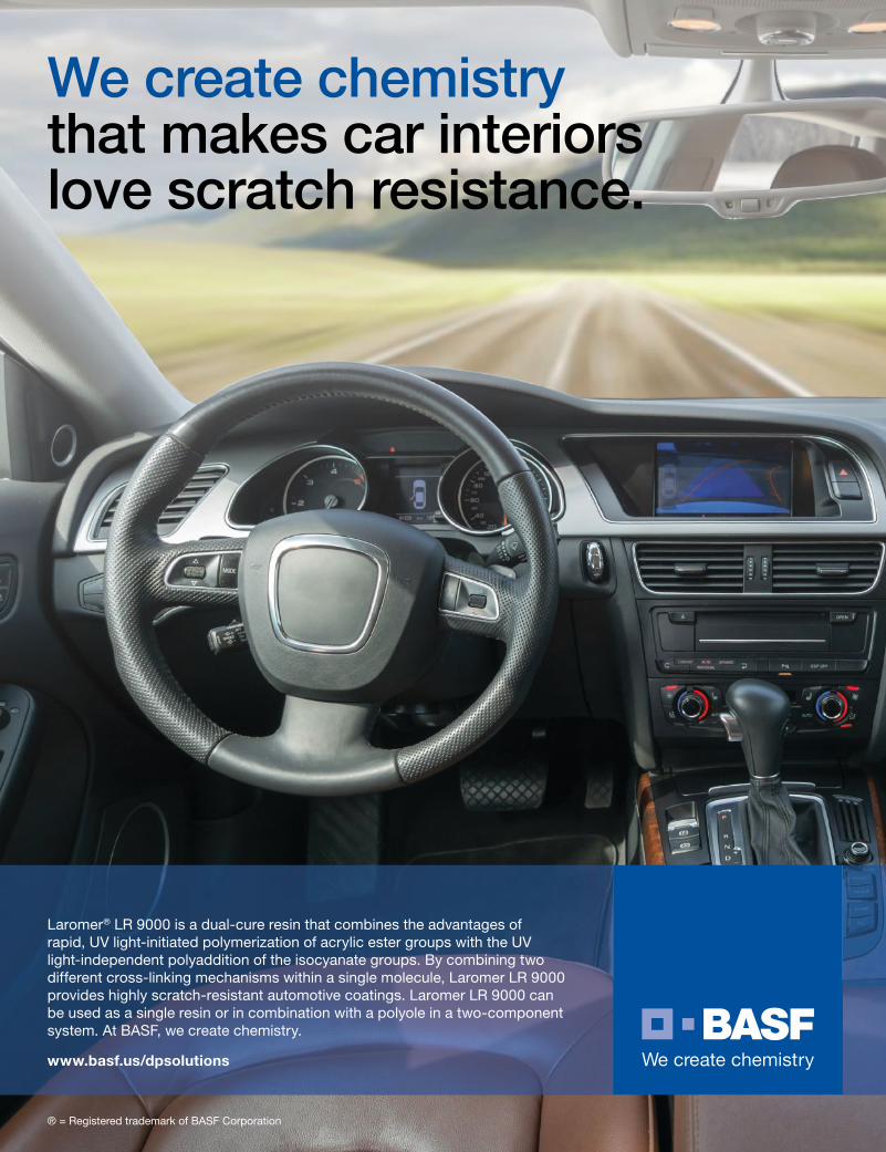
We create chemistry that makes car interiors love scratch resistance.
Laromer® LR 9000 is a dual-cure resin that combines the advantages of rapid, UV light-initiated polymerization of acrylic ester groups with the UV light-independent polyaddition of the isocyanate groups. By combining two different cross-linking mechanisms within a single molecule, Laromer LR 9000 provides highly scratch-resistant automotive coatings. Laromer LR 9000 can be used as a single resin or in combination with a polyole in a two-component system. At BASF, we create chemistry.
www.basf.us/dpsolutions
® = Registered trademark of BASF Corporation

2 | UV+EB Technology • Issue 1, 2017 uvebtechnology.com + radtech.org
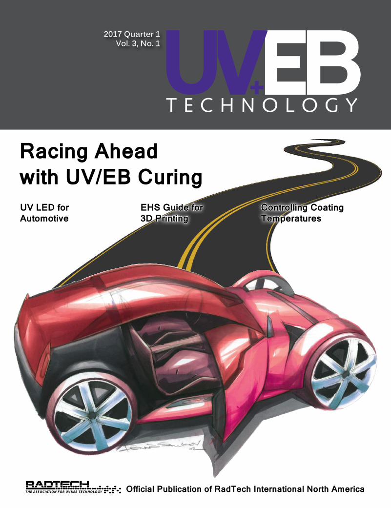
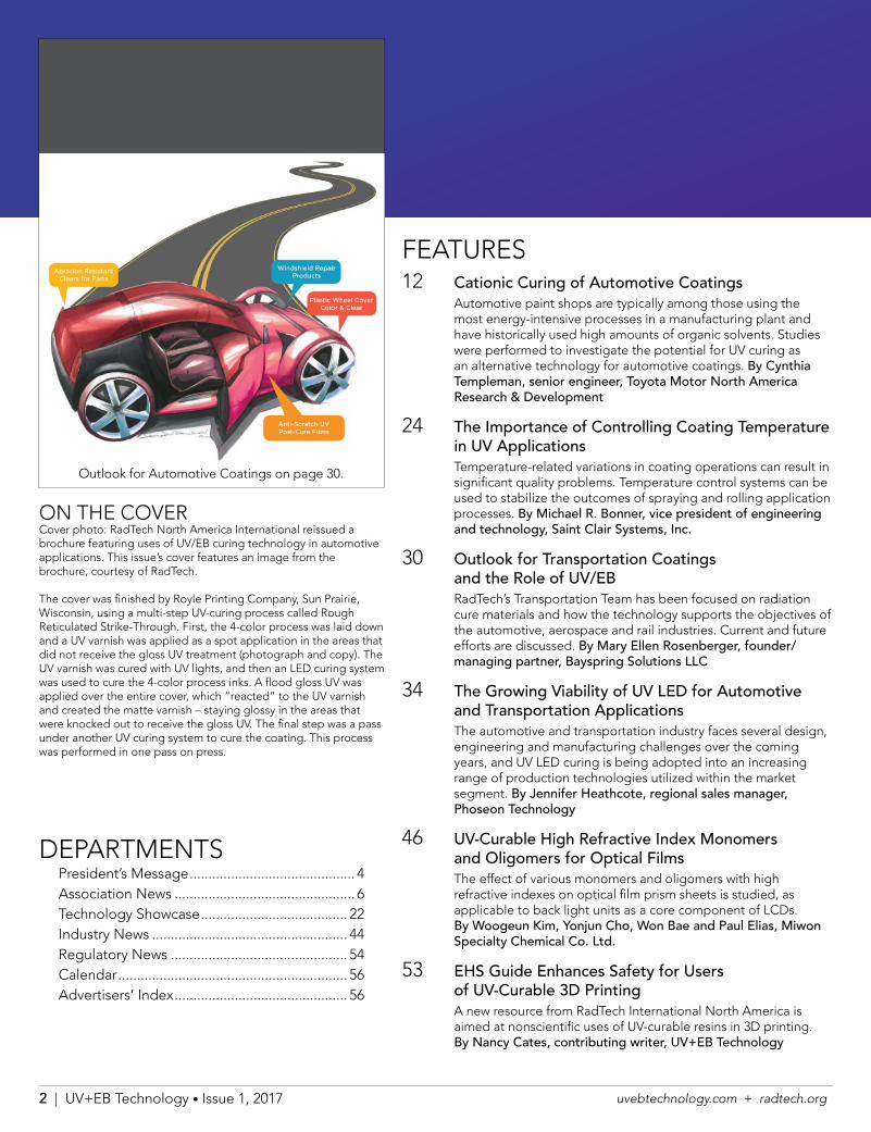
ON THE COVERCover photo: RadTech North America International reissued a brochure featuring uses of UV/EB curing technology in automotive applications. This issue’s cover features an image from the brochure, courtesy of RadTech.
The cover was finished by Royle Printing Company, Sun Prairie, Wisconsin, using a multi-step UV-curing process called Rough Reticulated Strike-Through. First, the 4-color process was laid down and a UV varnish was applied as a spot application in the areas that did not receive the gloss UV treatment (photograph and copy). The UV varnish was cured with UV lights, and then an LED curing system was used to cure the 4-color process inks. A flood gloss UV was applied over the entire cover, which “reacted” to the UV varnish and created the matte varnish – staying glossy in the areas that were knocked out to receive the gloss UV. The final step was a pass under another UV curing system to cure the coating. This process was performed in one pass on press.
FEATURES12 Cationic Curing of Automotive Coatings
Automotive paint shops are typically among those using the most energy-intensive processes in a manufacturing plant and have historically used high amounts of organic solvents. Studies were performed to investigate the potential for UV curing as an alternative technology for automotive coatings. By Cynthia Templeman, senior engineer, Toyota Motor North America Research & Development
24 The Importance of Controlling Coating Temperature in UV Applications
Temperature-related variations in coating operations can result in significant quality problems. Temperature control systems can be used to stabilize the outcomes of spraying and rolling application processes. By Michael R. Bonner, vice president of engineering and technology, Saint Clair Systems, Inc.
30 Outlook for Transportation Coatings and the Role of UV/EB
RadTech’s Transportation Team has been focused on radiation cure materials and how the technology supports the objectives of the automotive, aerospace and rail industries. Current and future efforts are discussed. By Mary Ellen Rosenberger, founder/managing partner, Bayspring Solutions LLC
34 The Growing Viability of UV LED for Automotive and Transportation Applications
The automotive and transportation industry faces several design, engineering and manufacturing challenges over the coming years, and UV LED curing is being adopted into an increasing range of production technologies utilized within the market segment. By Jennifer Heathcote, regional sales manager, Phoseon Technology
46 UV-Curable High Refractive Index Monomers and Oligomers for Optical Films
The effect of various monomers and oligomers with high refractive indexes on optical film prism sheets is studied, as applicable to back light units as a core component of LCDs. By Woogeun Kim, Yonjun Cho, Won Bae and Paul Elias, Miwon Specialty Chemical Co. Ltd.
53 EHS Guide Enhances Safety for Users of UV-Curable 3D Printing
A new resource from RadTech International North America is aimed at nonscientific uses of UV-curable resins in 3D printing. By Nancy Cates, contributing writer, UV+EB Technology
DEPARTMENTSPresident’s Message ............................................ 4Association News ................................................ 6Technology Showcase ....................................... 22Industry News .................................................... 44Regulatory News ............................................... 54Calendar ............................................................. 56Advertisers’ Index .............................................. 56
Outlook for Automotive Coatings on page 30.

uvebtechnology.com + radtech.org UV+EB Technology • Issue 1, 2017 | 3
T E C H N O L O G Y
COLUMN8 UV Curing Technology Question & Answer How Can the Orientation of UV Lamps in a 3D Curing System be Described? By R.W. Stowe, director of applications engineering, Heraeus Noblelight America LLC
10 EB Curing Technology Question & Answer What are the most common consumable costs encountered when operating a low-energy EB system? By Anthony Carignano, director, sales – Americas, ebeam Technologies
CHAMPIONS THIS ISSUE RadTech International North America’s Editorial Board facilitates the technical articles featured in UV+EB Technology. Smaller teams of Issue Champions review and approve articles and provide overall content management for each issue, as needed. If you are a member of RadTech and are interested in serving on the Editorial Board, contact Gary Cohen at [email protected].
2017 Quarter 1Vol. 3, No. 1
Mike Higgins East Regional Sales Manager
Phoseon Technology
Susan Bailey, IGM ResinsCo-Chair/Editor-in-Chief
Syed Hasan, BASF CorporationCo-Chair/Editor-in-Chief
Brian Cavitt, Lipscomb UniversityByron Christmas, Professor of Chemistry, RetiredCharlie He, Full Spectrum Laser LLCMike Higgins, Phoseon TechnologyMolly Hladik, ACTEGA North America
Mike J. Idacavage, Colorado Photopolymer SolutionsJin Lu, SartomerSudhakar Madhusoodhanan, ValsparGary Sigel, Armstrong FlooringMaria Muro-Small, Spectra Group Limited, Inc.R.W. Stowe, Heraeus Noblelight America LLCHuanyu Wei, ITW Sports Branding DivisionJinping Wu, PolyOne CorporationSheng “Sunny” Ye, 3M
UV+EB TECHNOLOGY EDITORIAL BOARD
Maria Muro-Small Director of Marketing
Spectra Group Limited, Inc.
Sheng “Sunny” Ye Senior Research Engineer 3M Corporate Research Process Laboratory - UV
Processing Group
Susan Bailey Technical Development
Manager, Acrylates IGM Resins
Syed T. Hasan Editorial Board Co-Chair Key Account Manager,
Security Inks BASF Corporation
Jin LuManager, Adhesive Sealant & Personal Care Platform
Sartomer

4 | UV+EB Technology • Issue 1, 2017 uvebtechnology.com + radtech.org
President’s Message
2150 SW Westport Drive, Suite 101Topeka, Kansas 66614785-271-5801petersonpublications.com
Publisher National Sales DirectorJeff Peterson Janet Dunnichay [email protected]
Art Director Managing Editor Becky Arensdorf Dianna Brodine [email protected]
Contributing Editors Circulation ManagerLara Copeland Brenda SchellNancy Cates [email protected] ENews & Website DeveloperJen Clark
Published by:
An official publication of:RADTECH INTERNATIONAL NORTH AMERICA7758 Wisconsin Avenue, Suite 302Bethesda, Maryland 20814240-497-1242radtech.org
EXECUTIVE DIRECTORGary M. [email protected]
SENIOR DIRECTORMickey Fortune
BOARD OF DIRECTORSPresidentLisa Fine – Joules Angstrom UV Printing Inks
President-electEileen Weber – Red Spot
SecretaryJennifer Heathcote – Phoseon Technology
TreasurerPaul Elias – Miwon North America
Immediate Past-PresidentPeter Weissman – Quaker Chemical Corporation
Board of DirectorsJo Ann Arceneaux – Allnex USA Inc.Susan Bailey – IGM ResinsMark Gordon – INX International Ink CompanyDavid Biro – Sun ChemicalMichael Gould – Rahn USAGeorge McGill – Zeller + Gmelin CorporationAlexander Polykarpov – AkzoNobelBeth Rundlett – Katecho, Inc.Chris Seubert – Ford Motor CompanyAlrick “Al” Warner – Procter and GambleXiasong Wu – DSM Functional Materials
T E C H N O L O G Y
Lisa Fine
As I begin my term as president of RadTech, the first thing I would like to do is acknowledge other folks. It is
through their willingness to serve and their dedicated efforts that RadTech has been able to grow and adapt to the constantly changing technical and regulatory climates.
Congratulations to our new president-elect, Eileen Weber of Red Spot. Eileen has been a board member for many years and has served as our secretary as well. We appreciate all she has done for the RadTech organization and for the industry and look forward to having her as our leader in the next term.
Next, a warm welcome to our new board members: Susan Bailey of IGM Resins, Michael Gould of Rahn USA, David Biro of Sun Chemical and Chris Seubert of Ford Motor Company. I also would like to thank our Printing and Packaging Committee, member volunteers and Doreen Monteleone for their support in our all-new UV/EB Printer’s Resource Guide on the RadTech website.
As we roll into 2017, regulatory issues will remain a focus of our collective attention. TSCA reform and Proposition 65 legislation continue to evolve, just to name a couple of items. It is through our awareness and understanding of these issues that we can help our members navigate this ever-changing landscape.
There also is continued excitement on the technology side: next-generation inkjet and 3D printing, as well as evolving capabilities of LED curing, are engaging the innovators in our industry. The attendance and enthusiasm we experienced at RadTech 2016 is certainly carrying over to uv.ebWEST, as we have had an early and overwhelming response to the program by exhibitors and interested parties.
Also, RadTech members, through The RadTech Foundation, are working with Poly6 Technologies – a UV/EB start-up in the MIT Accelerator – to reach out to other start-ups interested in using our technology to share knowledge and contacts.
Education is the cornerstone of our efforts and, to this end, I want to thank Mike Idacavage for developing the first of our “10-Minute Online Courses.” The UV/EB technology course is in email format and is free to attendees. At the end of the eight lessons, RadTech will email a certificate that attendees can post on their LinkedIn profiles. The idea is to help inform those who are interested in UV and/or EB curing but do not have a technical background in our industry. The typical attendee would be someone in marketing, sales or customer service… or perhaps a lab technician or scientist who is new to the technology and wants a high-level overview. In addition to the inaugural course (“UV/EB Chemistry Fundamentals”), we also will be developing courses in LED technology and EHS issues germane to our industry.
Providing this educational benefit not only raises awareness of our industry and our organization but also helps RadTech identify the reach of UV/EB technology. After all, as the market for UV+EB continues to expand into new applications, and established end-uses gain market share, companies involved in a range of activities are working to learn about and support the use of our technology.
In summary, there has never been a better time for innovation than the present. I am looking forward to an exciting year ahead!
Lisa FinePresident, RadTech International North AmericaJoules Angstrom UV Printing Inks
We unlock the potential of UV/LED light and transform its power You have a unique curing need, the product specifications are extremely precise, and the manufacturing process runs 24/7. You need a UV/LED curing specialist who understands your growing needs and will help you meet the demands of your ever-changing marketplace. For over two decades Honle UV America has been raising the bar in the development of new UV/LED curing technology that has made the printing, coating, and adhesive assembly industries worldwide more profitable. Our expertise lies in unlocking the potential of UV/LED light and transforming its power into a variety of custom engineered curing solutions that will maximize your productivity and profitability.
Our expert engineers are on hand for on-site evaluations, they’ll make recommendations on UV/LED equipment, and support you and your staff throughout the life of our products.
Come explore the transformation for yourself and see what makes our UV/LED curing technology a profitable solution for your growing business.
261 Cedar Hill Street, Marlboro, MA 01752508.229.7774 • www.honleuv.com
LED AC 410LED AC 820
LED Powerline
LED Cube 100
Jetcure LED

6 | UV+EB Technology • Issue 1, 2017 uvebtechnology.com + radtech.org
Association News
uv.eb WEST 2017 on its Way to San FranciscoThe uv.eb WEST 2017 Materials + Manufacturing Summit, February 27 through March 1 in San Francisco, California, features more than 50 exhibitors and conference sessions on
UV LED, 3D Printing: Market + Materials, UV Materials for Displays, Food Packaging + Disinfection and
Next Generation UV Inkjet Technology. The RadTech Annual Winter Meeting is co-located with the event, including committee meetings on 3D Printing, Printing and Packaging, Automotive, UV LED and Environmental Health and Safety. RadTech also will host two new committee meetings. The “Associate Member Committee” will discuss issues with companies that support raw material and equipment suppliers, formulators and end users of UV/EB. This new member category includes consultants, additive manufacturers and equipment and service providers that do not directly sell UV and/or EB curing equipment. In addition, the RadTech Foundation will have an open meeting to present the development of a RadTech Technology Accelerator to discuss the role RadTech plays as a mentor to UV+EB start-ups. The RadTech Annual Winter Meetings are March 1 and 2, co-located with uv.eb WEST.
RadTech Offers Free UV/EB E-CourseIn an effort to continue the mission to develop educational opportunities for UV+EB, RadTech has launched the first course in a series of free, email-based courses that will deliver educational lessons on various aspects of UV/EB technology. Each course will feature several lessons sent in a weekly email that should take roughly 10 minutes to read. After the final lesson, RadTech will email a course-completion certification that users can post on their LinkedIn profiles.
The first course in the offering is UV/EB Chemistry Fundamentals and features the following eight lessons:
Lesson 1: What Is UV/EB Curing?Lesson 2: Basic Chemistry of UV CuringLesson 3: Basic Materials Used in UV/EB CuringLesson 4: How Do Photoinitiators Work?Lesson 5: Equipment Used in UV/EB CuringLesson 6: Environmental Handling & SafetyLesson 7: Graphic Arts ApplicationsLesson 8: Industrial Applications
RadTech Partners with Future EventsRadTech continues to partner with other groups and events to extend the reach of UV/EB. Upcoming activities include the following UV/EB technology conference sessions.• The Eastern Coatings Show in Atlantic City, New Jersey,
May 15 through 27, 2017.
• AWFS Fair, July 19 through 22, 2017, in Las Vegas, Nevada, featuring presentations from Ikea, Superfici, EIT, Van Technologies, Phoseon and more.
• Photopolymerization Fundamentals 2017, September 17-20, in Boulder, Colorado.
New Board Members AnnouncedRadTech is pleased to announce that Lisa Fine of Joules Angstrom UV Printing Inks is assuming the presidency of RadTech International, the nonprofit for Ultraviolet and Electron Beam (UV/EB) Technologies, for a two-year term beginning January 1, 2017. Peter Weissman, Quaker Chemical Corp., will move to immediate past president. Eileen Weber of Red Spot Paint and Varnish has been nominated to serve as president elect and will assume office in 2019. New RadTech board members also have been elected, including Susan Bailey, IGM Resins; David Biro, Sun Chemical; and Michael Gould, RAHN USA. Also, Christopher M. Seubert, Ford Motor Co., has been elected to serve as an at-large board member.
Returning RadTech board members include Alexander Polykarpov, AkzoNobel; Jo Ann Arceneaux, Allnex USA Inc.; George McGill, Coatings and Adhesives Corp.; Xiaosong Wu, DSM Functional Materials; Mark Gordon, Inx International Ink Co.; Beth Rundlett, Katecho Inc.; Paul Elias, Miwon North America; Jennifer Heathcote, Phoseon Technology; and Alrick Warner, Procter and Gamble.
RadTech Sponsors Design Contest for Safety PosterThe design work of Josh Brdicko, a graphic design and art education major at the University of Iowa, was chosen for RadTech International North America’s UV 3D Printing Safe Handling Guide (see article on page 53). Brdicko currently works as a graphic designer at the University of Iowa for the Iowa Memorial Union marketing and design team and, upon graduation, hopes to teach art and design. “After the work of Mike Idacavage and the RadTech 3D Printing Committee to develop our safety poster, it was decided that proper design would be important to ensure its use and help us make an impact,” said Gary Cohen, executive director of RadTech International North America. “Julie Jessop of the University of Iowa connected with the design department at her school, and the idea of a student design competition was hatched.” RadTech was pleased to receive creative entries from five students, each providing their own interpretation of the poster. Brdicko’s design was chosen by an internal committee. u

For further information please contact us on: [email protected]
UK +44 1737 824 500 Germany +49 7022 303 9769 USA +1 440 237 4439 India +91 22 2528 5442
gewuv.com
hybridArcLED®
LED
Arc
RHINO
Air-cooled LED and arc lamp systems…...driven by RHINO ArcLED power electronics: the only future-proof UV technology with true arc lamp and LED compatibility, supported by the security of a 5-year warranty.
TWO UV Curing TechnologiesONE RHINO Power SupplyNOW Fully Air-cooled

8 | UV+EB Technology • Issue 1, 2017 uvebtechnology.com + radtech.org
Q. How Can the Orientation of UV Lamps in a 3D Curing System be Described?
A.
UV CURING TECHNOLOGYQUESTION & ANSWER
R.W. StoweUV Applications Engineering Consultant
Heraeus Noblelight America LLC [email protected]
There is a useful language.
Life in the UV curing world was easier when UV lamps only stretched across a web or flat conveyor, and all we had to worry about was width, number of rows and distance from the work. But, as we move into 3D processing of complex shaped objects, lamps are located all over the curing zone. In fixed-lamp 3D configurations, each lamp has its own optimized position. Setting lamps in a large 3D installation falls somewhere between science and art.
Chain-on-edge systems and paint lines represent a whole family of problems in orienting the UV lamps. The line can be continually moving or intermittent. The parts can be rotating or not. The solutions to lamp positioning to provide uniform exposure to all (or most) of the surfaces can be quite complex. But, let’s stick to the question of describing lamp orientation.
Have you ever tried to describe the orientation of a UV lamp – or several lamps – in a 3D configuration? Have you watched an otherwise conservative engineer waving his hands and arms, often with the assistance of pens (to represent bulbs) and file cards (curved, to represent reflectors), trying to communicate the orientation of a lamp in space? What about changing the position of a lamp? Does it drive you nuts to hear the description of “Just rotate the lamp a little?” “Rotate? What does THAT mean?” “You know ... tilt it ... at an angle.” Uh-oh.
Some time ago, it struck me that describing how to orient something in space isn’t a new problem. There is a language that is clear and that we can adapt easily to 3D lamp orientation. It’s used all the time in flight and aerospace situations. There are two parts: attitude and position.
AttitudeThink airplane. We begin with pitch, yaw and roll. For the pilot of an airplane, pitch is the angle relative to a plane, for example, the horizon: nose up, nose down or level. Yaw is turning right or left. Roll is raising one wing and lowering the other. These three axes will completely describe the attitude of the aircraft.
Think of the axis of the UV bulb aligned with the wingspan of the aircraft, and you get the idea.
PositionThis is a little trickier, because there are several ways to locate a point in space. First, the principal axis is along the direction of travel of the production line. The principal axis can be located anywhere parallel to the travel. The centerline of the conveyor and the floor, for example, are convenient reference points for locating the principal axis.
Imagine a horizontal plane through this principal axis. This is like the horizon. A point can be located by its height (altitude) from the plane and its horizontal distance from the centerline (Cartesian coordinates). Another way to locate the point is to use its angle of elevation from the “horizon” plane and the distance to the principal axis. Pick one of these ways and stick with it.
By locating the position of a point in space and describing the attitude of the object at that point, its precise orientation can be described and communicated – or drawn – consistently. And, this method of description is independent of the complexities of object shapes and surfaces to be cured. (How many and where to locate lamps for maximum effectiveness is a topic for another day.)
Now, if this doesn’t make it easier, maybe some pencils and some file cards … u
distance
height
distance
angle

10 | UV+EB Technology • Issue 1, 2017 uvebtechnology.com + radtech.org
EB CURING TECHNOLOGYQUESTION & ANSWER
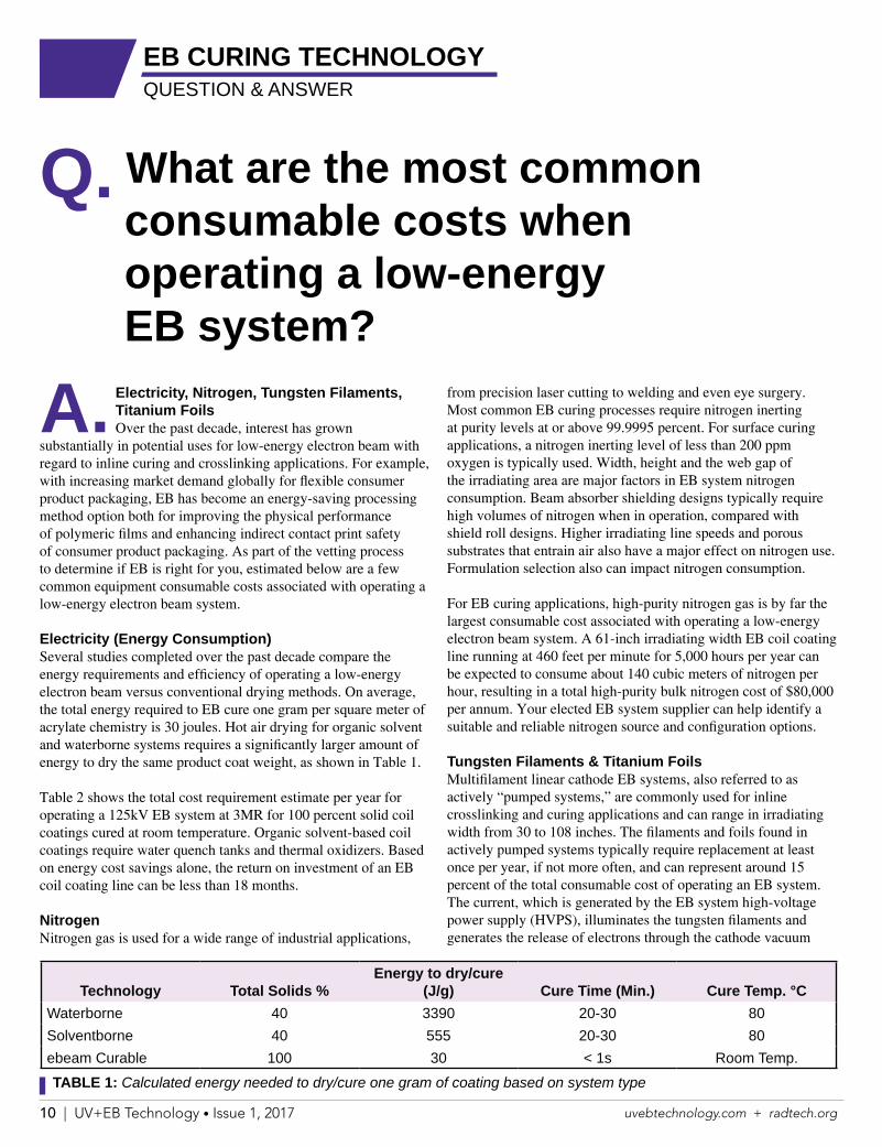
Electricity, Nitrogen, Tungsten Filaments, Titanium Foils Over the past decade, interest has grown
substantially in potential uses for low-energy electron beam with regard to inline curing and crosslinking applications. For example, with increasing market demand globally for flexible consumer product packaging, EB has become an energy-saving processing method option both for improving the physical performance of polymeric films and enhancing indirect contact print safety of consumer product packaging. As part of the vetting process to determine if EB is right for you, estimated below are a few common equipment consumable costs associated with operating a low-energy electron beam system.
Electricity (Energy Consumption) Several studies completed over the past decade compare the energy requirements and efficiency of operating a low-energy electron beam versus conventional drying methods. On average, the total energy required to EB cure one gram per square meter of acrylate chemistry is 30 joules. Hot air drying for organic solvent and waterborne systems requires a significantly larger amount of energy to dry the same product coat weight, as shown in Table 1.
Table 2 shows the total cost requirement estimate per year for operating a 125kV EB system at 3MR for 100 percent solid coil coatings cured at room temperature. Organic solvent-based coil coatings require water quench tanks and thermal oxidizers. Based on energy cost savings alone, the return on investment of an EB coil coating line can be less than 18 months.
Nitrogen Nitrogen gas is used for a wide range of industrial applications,
Q. What are the most common consumable costs when operating a low-energy EB system?
A. from precision laser cutting to welding and even eye surgery. Most common EB curing processes require nitrogen inerting at purity levels at or above 99.9995 percent. For surface curing applications, a nitrogen inerting level of less than 200 ppm oxygen is typically used. Width, height and the web gap of the irradiating area are major factors in EB system nitrogen consumption. Beam absorber shielding designs typically require high volumes of nitrogen when in operation, compared with shield roll designs. Higher irradiating line speeds and porous substrates that entrain air also have a major effect on nitrogen use. Formulation selection also can impact nitrogen consumption.
For EB curing applications, high-purity nitrogen gas is by far the largest consumable cost associated with operating a low-energy electron beam system. A 61-inch irradiating width EB coil coating line running at 460 feet per minute for 5,000 hours per year can be expected to consume about 140 cubic meters of nitrogen per hour, resulting in a total high-purity bulk nitrogen cost of $80,000 per annum. Your elected EB system supplier can help identify a suitable and reliable nitrogen source and configuration options.
Tungsten Filaments & Titanium Foils Multifilament linear cathode EB systems, also referred to as actively “pumped systems,” are commonly used for inline crosslinking and curing applications and can range in irradiating width from 30 to 108 inches. The filaments and foils found in actively pumped systems typically require replacement at least once per year, if not more often, and can represent around 15 percent of the total consumable cost of operating an EB system. The current, which is generated by the EB system high-voltage power supply (HVPS), illuminates the tungsten filaments and generates the release of electrons through the cathode vacuum
Technology Total Solids %Energy to dry/cure
(J/g) Cure Time (Min.) Cure Temp. °CWaterborne 40 3390 20-30 80Solventborne 40 555 20-30 80ebeam Curable 100 30 < 1s Room Temp.
TABLE 1: Calculated energy needed to dry/cure one gram of coating based on system type

uvebtechnology.com + radtech.org UV+EB Technology • Issue 1, 2017 | 11
Anthony Carignano Director, Sales – Americas,
ebeam Technologies anthony.carignano@ ebeamtechnologies.com
Comparative Energy Cost Estimate(61" wide inline process at 460 feet per minute for 5,000 hours/year)
Power Used (kW) IR (SW) NIR Induction Convection UV ebeamPrimer Oven 4400 3800 4200 7000 365Top Coat Oven 4250 3850 4300 7300 48Air Recirculation 350 300 420 75 60Water Quench 75 75 75 120Themal Oxidizer 1140 1140 1140 1140Electricity Cost ($0.058 / kWh)
$526.4 $465.5 $521.7 $836.4 $25.5 $6.3
NG Cost ($0.032 / kWh)
$36.5 $36.5 $36.5 $36.5 $0.0 $0.0
Energy Cost US$M/Year $2.81 $2.51 $2.79 $4.36 $0.13 $0.031
chamber and titanium foil. After either the mass of the filament is depleted through its release of electrons, or because there is poor vacuum inside the vacuum chamber, filaments eventually fail and must be replaced. Under optimum conditions, tungsten filaments will last up to 10 months.
Titanium window foils cover the full irradiating width of the electron beam and are supported by a copper cooling grid (Figure 1). Certain EB system designs require the replacement of one continuous foil. Other systems require the replacement of two foils per system. Titanium foil replacement is typically completed by a technician who is well trained in the art of not creasing foils that can range in total thickness from 10 to 15 microns. The average life of the titanium window that faces the shielded surface of the EB is four to six months. Improper installation, quality of consistent vacuum, efficient transfer of heat away from the foil window and arcing caused by temporary lapses in voltage are
FIGURE 1: ebeam Technologies LE Series Shield Roll design titanium foil mounted on copper cooling grid.
variables that can affect foil life. To minimize downtime and maximize EB performance, the filaments and foils on pumped systems are typically replaced at the same time and can cost approximately 10 percent of the total operating cost, depending on the width of the irradiating width of the electron beam.
Unlike pumped systems, sealed “EB lamp” systems contain a single cathode filament tube. Much like a light bulb, the entire lamp is replaced when spent and thus considered a consumable. Depending on usage, sealed EB lamps have an average life of greater than 8,000 continuous hours and generate electrons under the same principals as pumped systems. It is anticipated that the cost of sealed EB lamps will decrease substantially over the next three years as demand increases, driven by surface sterilization, narrow web finishing and ultralow migration inkjet printing applications.
The conclusion to this discussion is that EB systems represent a highly energy efficient method for instantaneously surface curing and crosslinking polymeric substrates. The EB curing requires a source of high-purity nitrogen for surface inerting to minimize the potential for oxygen inhibition during the free radical polymerization process. Nitrogen is the major consumable cost in operating EB but can be minimized through optimized system design. Tungsten filaments and titanium foils also are consumable items required to operate a low-energy electron beam and also are affected by EB equipment design and performance. u
TABLE 2: Comparative energy cost estimates. Calculations provided by ebeam Technologies’ engineering group.
12 | UV+EB Technology • Issue 1, 2017 uvebtechnology.com + radtech.org
CATIONIC CURING
By Cynthia Templeman, Senior Engineer, Toyota Motor North America Research & Development
Automotive paint shops are typically among those using the most energy-intensive processes in a manufacturing plant. Studies by Argonne National Lab (ANL/ESD/10-6), Michigan Technological
University (Automobile Assembly Painting: Energy and Environmental Impacts [John Sutherland]) and others estimate that 50 to 75 percent of the energy consumption and carbon dioxide emissions from “material transformations” for an assembly plant are directly related to paint, particularly for the painting, HVAC and heating. Besides energy and carbon dioxide emissions, paint shops also historically have used high amounts of organic solvents.
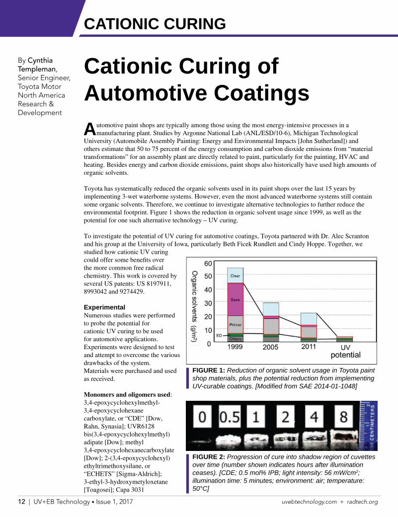
Toyota has systematically reduced the organic solvents used in its paint shops over the last 15 years by implementing 3-wet waterborne systems. However, even the most advanced waterborne systems still contain some organic solvents. Therefore, we continue to investigate alternative technologies to further reduce the environmental footprint. Figure 1 shows the reduction in organic solvent usage since 1999, as well as the potential for one such alternative technology – UV curing.
To investigate the potential of UV curing for automotive coatings, Toyota partnered with Dr. Alec Scranton and his group at the University of Iowa, particularly Beth Ficek Rundlett and Cindy Hoppe. Together, we studied how cationic UV curing could offer some benefits over the more common free radical chemistry. This work is covered by several US patents: US 8197911, 8993042 and 9274429.
ExperimentalNumerous studies were performed to probe the potential for cationic UV curing to be used for automotive applications. Experiments were designed to test and attempt to overcome the various drawbacks of the system.Materials were purchased and used as received.
Monomers and oligomers used: 3,4-epoxycyclohexylmethyl-3,4-epoxycyclohexane carboxylate, or “CDE” [Dow, Rahn, Synasia]; UVR6128 bis(3,4-epoxycyclohexylmethyl) adipate [Dow]; methyl 3,4-epoxycyclohexanecarboxylate [Dow]; 2-(3,4-epoxycyclohexyl)ethyltrimethoxysilane, or “ECHETS” [Sigma-Aldrich]; 3-ethyl-3-hydroxymetyloxetane [Toagosei]; Capa 3031
Cationic Curing of Automotive Coatings
FIGURE 1: Reduction of organic solvent usage in Toyota paint shop materials, plus the potential reduction from implementing UV-curable coatings. [Modified from SAE 2014-01-1048]
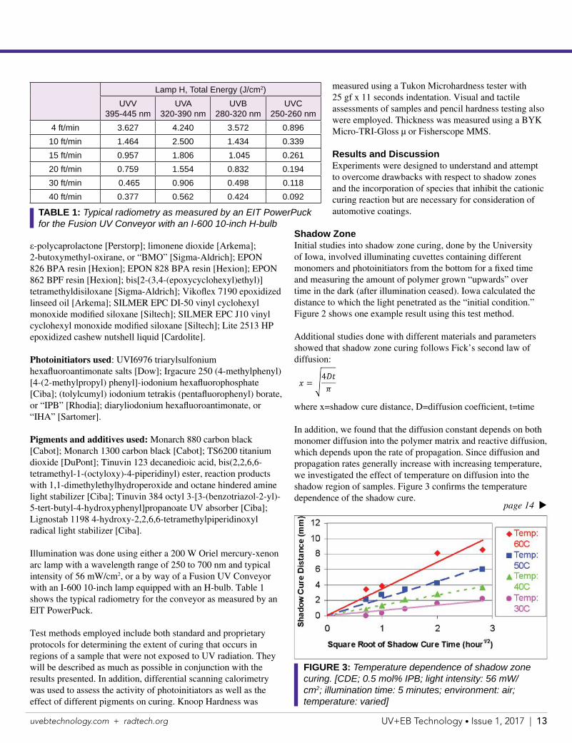
FIGURE 2: Progression of cure into shadow region of cuvettes over time (number shown indicates hours after illumination ceases). [CDE; 0.5 mol% IPB; light intensity: 56 mW/cm2; illumination time: 5 minutes; environment: air; temperature: 50°C]
uvebtechnology.com + radtech.org UV+EB Technology • Issue 1, 2017 | 13
ε-polycaprolactone [Perstorp]; limonene dioxide [Arkema]; 2-butoxymethyl-oxirane, or “BMO” [Sigma-Aldrich]; EPON 826 BPA resin [Hexion]; EPON 828 BPA resin [Hexion]; EPON 862 BPF resin [Hexion]; bis[2-(3,4-(epoxycyclohexyl)ethyl)]tetramethyldisiloxane [Sigma-Aldrich]; Vikoflex 7190 epoxidized linseed oil [Arkema]; SILMER EPC DI-50 vinyl cyclohexyl monoxide modified siloxane [Siltech]; SILMER EPC J10 vinyl cyclohexyl monoxide modified siloxane [Siltech]; Lite 2513 HP epoxidized cashew nutshell liquid [Cardolite].
Photoinitiators used: UVI6976 triarylsulfonium hexafluoroantimonate salts [Dow]; Irgacure 250 (4-methylphenyl)[4-(2-methylpropyl) phenyl]-iodonium hexafluorophosphate [Ciba]; (tolylcumyl) iodonium tetrakis (pentafluorophenyl) borate, or “IPB” [Rhodia]; diaryliodonium hexafluoroantimonate, or “IHA” [Sartomer].
Pigments and additives used: Monarch 880 carbon black [Cabot]; Monarch 1300 carbon black [Cabot]; TS6200 titanium dioxide [DuPont]; Tinuvin 123 decanedioic acid, bis(2,2,6,6-tetramethyl-1-(octyloxy)-4-piperidinyl) ester, reaction products with 1,1-dimethylethylhydroperoxide and octane hindered amine light stabilizer [Ciba]; Tinuvin 384 octyl 3-[3-(benzotriazol-2-yl)-5-tert-butyl-4-hydroxyphenyl]propanoate UV absorber [Ciba]; Lignostab 1198 4-hydroxy-2,2,6,6-tetramethylpiperidinoxyl radical light stabilizer [Ciba].
Illumination was done using either a 200 W Oriel mercury-xenon arc lamp with a wavelength range of 250 to 700 nm and typical intensity of 56 mW/cm2, or a by way of a Fusion UV Conveyor with an I-600 10-inch lamp equipped with an H-bulb. Table 1 shows the typical radiometry for the conveyor as measured by an EIT PowerPuck.
Test methods employed include both standard and proprietary protocols for determining the extent of curing that occurs in regions of a sample that were not exposed to UV radiation. They will be described as much as possible in conjunction with the results presented. In addition, differential scanning calorimetry was used to assess the activity of photoinitiators as well as the effect of different pigments on curing. Knoop Hardness was
Lamp H, Total Energy (J/cm2)
UVV 395-445 nm
UVA 320-390 nm
UVB 280-320 nm
UVC 250-260 nm
4 ft/min 3.627 4.240 3.572 0.896
10 ft/min 1.464 2.500 1.434 0.339
15 ft/min 0.957 1.806 1.045 0.261
20 ft/min 0.759 1.554 0.832 0.194
30 ft/min 0.465 0.906 0.498 0.118
40 ft/min 0.377 0.562 0.424 0.092
TABLE 1: Typical radiometry as measured by an EIT PowerPuck for the Fusion UV Conveyor with an I-600 10-inch H-bulb
measured using a Tukon Microhardness tester with 25 gf x 11 seconds indentation. Visual and tactile assessments of samples and pencil hardness testing also were employed. Thickness was measured using a BYK Micro-TRI-Gloss µ or Fisherscope MMS.
Results and DiscussionExperiments were designed to understand and attempt to overcome drawbacks with respect to shadow zones and the incorporation of species that inhibit the cationic curing reaction but are necessary for consideration of automotive coatings.
Shadow ZoneInitial studies into shadow zone curing, done by the University of Iowa, involved illuminating cuvettes containing different monomers and photoinitiators from the bottom for a fixed time and measuring the amount of polymer grown “upwards” over time in the dark (after illumination ceased). Iowa calculated the distance to which the light penetrated as the “initial condition.” Figure 2 shows one example result using this test method.
Additional studies done with different materials and parameters showed that shadow zone curing follows Fick’s second law of diffusion:
where x=shadow cure distance, D=diffusion coefficient, t=time
In addition, we found that the diffusion constant depends on both monomer diffusion into the polymer matrix and reactive diffusion, which depends upon the rate of propagation. Since diffusion and propagation rates generally increase with increasing temperature, we investigated the effect of temperature on diffusion into the shadow region of samples. Figure 3 confirms the temperature dependence of the shadow cure.
FIGURE 3: Temperature dependence of shadow zone curing. [CDE; 0.5 mol% IPB; light intensity: 56 mW/cm2; illumination time: 5 minutes; environment: air; temperature: varied]
page 14 u
14 | UV+EB Technology • Issue 1, 2017 uvebtechnology.com + radtech.org
t page 13
FIGURE 6: Distance to which polymerization proceeds into a masked region over time; various monomer mixtures. [0.75 wt% active UVR6976; 50 μm wet film thickness; ambient booth temperature 20°C and relative humidity 35%; see Experimental section for radiometry]
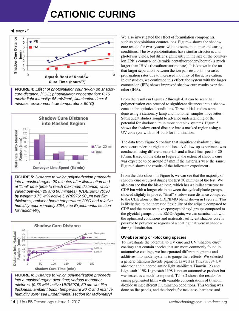
We also investigated the effect of formulation components, such as photoinitiator counter-ions. Figure 4 shows the shadow cure results for two systems with the same monomer and curing conditions. The two photoinitiators have similar structures and photolysis yields, but differ significantly in the size of the counter-ion. IPB’s counter-ion (tetrakis pentafluorophenylborate) is much larger than IHA’s (hexafluoroantimonate). It is known in the art that larger separation between the ion pair results in increased propagation rates due to increased mobility of the active cation. In our studies, we confirmed this effect: the system with the larger counter-ion (IPB) shows improved shadow cure results over the other (IHA).
From the results in Figures 2 through 4, it can be seen that polymerization can proceed to significant distances into a shadow zone under optimized conditions. These initial studies were done using a stationary lamp and monomer samples in cuvettes. Subsequent studies sought to advance understanding of the potential for shadow cure in more complex systems. Figure 5 shows the shadow-cured distance into a masked region using a UV conveyor with an H-bulb for illumination.
The data from Figure 5 confirm that significant shadow curing can occur under the right conditions. A follow-up experiment was conducted using different materials and a fixed line speed of 20 ft/min. Based on the data in Figure 5, the extent of shadow cure was expected to be around 27 mm if the materials were the same. Figure 6 shows the results of the follow-up experiment.
From the data shown in Figure 6, we can see that the majority of shadow cure occurred during the first 30 minutes of the test. We also can see that the bis-adipate, which has a similar structure to CDE but with a longer chain between the cycloaliphatic groups, showed slightly improved “final” shadow cure distance compared to the CDE alone or the CDE/BMO blend shown in Figure 5. This is likely due to the increased flexibility of the adipate compared to CDE and the more reactive epoxycyclohexyl groups compared to the glycidal groups on the BMO. Again, we can surmise that with the optimized conditions and materials, sufficient shadow cure is possible to polymerize regions of a coating that were in shadow during illumination.
UV-absorbing or -blocking speciesTo investigate the potential to UV cure and UV “shadow cure” coatings that contain species that are more commonly found in automotive coatings, we incorporated different pigments and additives into model systems to gauge their effects. We selected a generic titanium dioxide pigment, as well as Tinuvin 384 UV absorber and hindered amine light stabilizers Tinuvin 123 and Lignostab 1198. Lignostab 1198 is not an automotive product but was tested as a model compound. Table 2 shows the results for curing pigmented films with variable concentrations of titanium dioxide using different illumination conditions. This testing was done on flat panels, and the checks for tackiness, hardness and
FIGURE 4: Effect of photoinitiator counter-ion on shadow cure distance. [CDE; photoinitiator concentration: 0.75 mol%; light intensity: 56 mW/cm2; illumination time: 5 minutes; environment: air temperature: 50°C]
FIGURE 5: Distance to which polymerization proceeds into a masked region 20 minutes after illumination and at “final” time (time to reach maximum distance, which varied between 25 and 90 minutes). [CDE:BMO 70:30 by weight; 0.75 wt% active UVR6976; 50 μm wet film thickness; ambient booth temperature 20°C and relative humidity approximately 30%; see Experimental section for radiometry]
CATIONIC CURING

uvebtechnology.com + radtech.org UV+EB Technology • Issue 1, 2017 | 15
page 16 u
Siltech Corporation225 Wicksteed Avenue; Toronto, Ontario, Canada M4H 1G5Tel: (416) 424-4567; Fax: (416) 424-3158www.siltech.com
Need Some New Ideas?Servicing the Energy Cured
Coatings and 3D Printing Industrieswith unique silicone building blocks
Your Technology -Siltech Chemistry
Optimum PerformanceExcellent Customer Service
Innovative and Customized Products
thickness were done in the illuminated region (not a shadow region).
The results in Table 2 show that at low concentrations (1 to 3 percent by weight) the titanium dioxide did not inhibit the curing of the coating. Films were tack-free within the illumination time, and all had a high 3H hardness. With 6 percent by weight loading, tack-free times were longer, at 30 minutes, but the final films were equally hard as the films with lower loading. When exposure time is reduced for a fixed titanium dioxide concentration, tack-free times increase, as expected, but the films achieve higher final hardness. But allowing more of the polymerization to occur “in the dark,” it is surmised that less trapping of active centers occurs, allowing for a higher conversion and, therefore, an increased hardness (CDE monomer forms hard, rigid films).
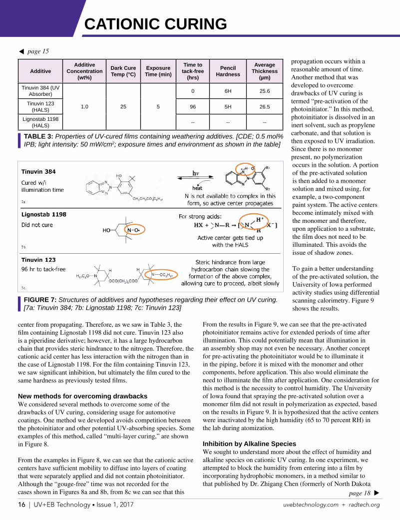
Table 3 shows similar data but for films loaded with other additives instead of titanium dioxide.
The data in Table 3 show that curing films containing additives to improve weathering performance, such as UV absorbers and hindered amine light stabilizers (HALS), is more challenging than films containing, for example, titanium dioxide. By nature, the UV absorbers compete with the photoinitiator during the illumination time. However, despite this competition, the film with Tinuvin 384 UV absorber still achieved a tack-free surface within the illumination time and resulted in a hard film. However, incorporating HALS seems to have a bigger effect on the ability of the film to cure. With Tinuvin 123, we can see considerable inhibition – with 96 hours being required to reach a tack-free surface – but the final film has similar hardness to those containing Tinuvin 384 or titanium dioxide. This suggests that, although the reaction rate is slower, final conversion is about the
same. The film containing Lignostab 1198 did not cure at all.
To understand these phenomena further, we looked at the structure of these additives, shown in Figure 7.
As shown in Figure 7, Tinuvin 384 is a benzotriazole-based UV absorber and, upon excitation with UV irradiation, the phenolic hydrogen is abstracted and adds to the adjacent nitrogen. Therefore, the nitrogen is not available to interfere directly with the propagating active center, and curing is able to proceed normally. The Lignostab 1198
is a radical form of a piperidine derivative. When strong acids, such as a cationic active center, are present, the acid interacts directly with the nitrogen. This effectively prevents the active
TiO2 Concentration
(wt%)
Dark Cure Temp (°C)
Exposure Time (min)
Time to tack-free (hrs)
Pencil Hardness
Average Thickness
(µm)
1.050
5
0 3H 40.8
25 0 3H 46.2
3.050 0 3H 37.5
25 0 3H 34.9
6.050 0.5 3H 33.8
25 0.5 3H 26.6
3.0 25
1 2 4H 31.0
2 1 4H 38.4
3 0.5 4H 38.0
4 0.5 5H 54.9
5 0 6H 52.8
TABLE 2: Properties of UV-cured films containing titanium dioxide at different concentrations. [CDE; 0.5 mol% IPB; light intensity: 50 mW/cm2; exposure times and environment as shown in the table]
16 | UV+EB Technology • Issue 1, 2017 uvebtechnology.com + radtech.org
t page 15
center from propagating. Therefore, as we saw in Table 3, the film containing Lignostab 1198 did not cure. Tinuvin 123 also is a piperidine derivative; however, it has a large hydrocarbon chain that provides steric hindrance to the nitrogen. Therefore, the cationic acid center has less interaction with the nitrogen than in the case of Lignostab 1198. For the film containing Tinuvin 123, we saw significant inhibition, but ultimately the film cured to the same hardness as previously tested films.
New methods for overcoming drawbacksWe considered several methods to overcome some of the drawbacks of UV curing, considering usage for automotive coatings. One method we developed avoids competition between the photoinitiator and other potential UV-absorbing species. Some examples of this method, called “multi-layer curing,” are shown in Figure 8.
From the examples in Figure 8, we can see that the cationic active centers have sufficient mobility to diffuse into layers of coating that were separately applied and did not contain photoinitiator. Although the “gouge-free” time was not recorded for the cases shown in Figures 8a and 8b, from 8c we can see that this
propagation occurs within a reasonable amount of time.Another method that was developed to overcome drawbacks of UV curing is termed “pre-activation of the photoinitiator.” In this method, photoinitiator is dissolved in an inert solvent, such as propylene carbonate, and that solution is then exposed to UV irradiation. Since there is no monomer present, no polymerization occurs in the solution. A portion of the pre-activated solution is then added to a monomer solution and mixed using, for example, a two-component paint system. The active centers become intimately mixed with the monomer and therefore, upon application to a substrate, the film does not need to be illuminated. This avoids the issue of shadow zones.
To gain a better understanding of the pre-activated solution, the University of Iowa performed activity studies using differential scanning calorimetry. Figure 9 shows the results.
From the results in Figure 9, we can see that the pre-activated photoinitiator remains active for extended periods of time after illumination. This could potentially mean that illumination in an assembly shop may not even be necessary. Another concept for pre-activating the photoinitiator would be to illuminate it in the piping, before it is mixed with the monomer and other components, before application. This also would eliminate the need to illuminate the film after application. One consideration for this method is the necessity to control humidity. The University of Iowa found that spraying the pre-activated solution over a monomer film did not result in polymerization as expected, based on the results in Figure 9. It is hypothesized that the active centers were inactivated by the high humidity (65 to 70 percent RH) in the lab during atomization.
Inhibition by Alkaline SpeciesWe sought to understand more about the effect of humidity and alkaline species on cationic UV curing. In one experiment, we attempted to block the humidity from entering into a film by incorporating hydrophobic monomers, in a method similar to that published by Dr. Zhigang Chen (formerly of North Dakota
AdditiveAdditive
Concentration (wt%)
Dark Cure Temp (°C)
Exposure Time (min)
Time to tack-free
(hrs)
Pencil Hardness
Average Thickness
(µm)
Tinuvin 384 (UV Absorber)
1.0 25 5
0 6H 25.6
Tinuvin 123 (HALS) 96 5H 26.5
Lignostab 1198 (HALS) -- -- --
TABLE 3: Properties of UV-cured films containing weathering additives. [CDE; 0.5 mol% IPB; light intensity: 50 mW/cm2; exposure times and environment as shown in the table]
FIGURE 7: Structures of additives and hypotheses regarding their effect on UV curing. [7a: Tinuvin 384; 7b: Lignostab 1198; 7c: Tinuvin 123]
page 18 u
CATIONIC CURING

18 | UV+EB Technology • Issue 1, 2017 uvebtechnology.com + radtech.org
State University) in RadTech 2008 proceedings. We prepared two panels each of five different formulations, cured them and then stored the panels in either a desiccator or in a controlled humidity environment (20°C, 50% RH) for one week. Knoop hardness was measured on the panels after one week of storage. The results are shown in Figure 10.
From the results in Figure 10, we can see that some of the reactive diluents added to the CDE seemed to have a humidity blocking
effect. Samples B and E showed similar hardness after both high and low humidity storage conditions. Samples A, C and D all resulted in untestable, peeled films from the high humidity conditions. So, we can understand that some components can be added to a formulation to make it more resistant to humidity.
We also studied the method of using the humidity within the film. Many groups are incorporating sol-gel precursors into UV-curable formulations as a way to add a means of crosslinking in
shadow zones, or possibly to add new functionality to materials. We looked at these materials as a means of overcoming inhibition by humidity. A series of formulations were prepared with varying amounts of the sol-gel precursor (SGP) ECHETS, and films were monitored for hardness initially and after one week. Again, we stored films in either a desiccator or in 50 percent RH controlled environment. Figure 11 shows the results.
From the data in Figure 11, we can see that the sol-gel precursor effectively protects the film from inhibition due to humidity. There is no difference in hardness seen between samples that were stored in high humidity compared to samples stored in low humidity.
t page 16
FIGURE 8: Some example configurations for curing multiple layers of coatings with photoinitiator (PI) present in only one layer. 8a: bottom layer CDE 70 wt%, BMO 29 wt%, 1 wt% IPB; top layer CDE 70 wt%, BMO 30 wt%. 8b:.bottom layer CDE 70 wt%, BMO 30 wt%; top layer CDE 70 wt%, BMO 29 wt%, IPB 1 wt%. 8c: top and bottom layers UVR6128 53.1 wt%, Vikoflex 7190 42.2 wt%, limonene dioxide 4.7 wt%; middle layer UVR6128 85.5 wt%, Vikoflex 7190 9.3 wt%, UVR6976 5.2 wt%. [Ambient lab conditions for all cases]
FIGURE 9: Reactivity of pre-activated photoinitiator. 9a: rate of polymerization measured on samples of monomer plus pre-activated photoinitiator that has been stored for various times at 25°C. 9b: summary of the maximum rate of polymerization for each different storage time. [10 to 15 mg BTS monomer plus 5 µl pre-activated photoinitiator solution (dropped on top of monomer); reaction temperature held constant at 50°C in a Perkin-Elmer DSC-7]
page 20 u
CATIONIC CURING

SARTOMER PA R T N E R SLET’S FORMULATE TOGETHER.SM
Visit us at uv.eb WEST February 28 – March 1 Burlingame, CA
sartomer.com
You’re passionate about your formulations. We are, too. Our tech support team contributes ingenious chemistry to advance performance in a wide host of applications. Think electronics, soft-touch coatings and automotive adhesives, just to name a few.
Formulators come to us for our unique expertise in acrylate and methacrylate chemistry. We lead the world with the broadest product portfolio for UV/EB/dual cure technology. But, it’s our interactive chemist-to-chemist support program that distinguishes us from the rest.
Our technologists understand your needs and create customized and innovative solutions to reach your specific formulation, processing and performance goals.
Follow us on:
© A
rkem
a In
c. 2
017
20 | UV+EB Technology • Issue 1, 2017 uvebtechnology.com + radtech.org
t page 18Finally, we studied the effect of pigment surface treatment on cationic UV curing. Two carbon black pigments (Monarch 880 and Monarch 1300) were incorporated into formulations. One of these has an acidic surface treatment, and the other has an alkaline surface treatment. We used photo-DSC (TA Instruments Q100) to grasp their effect on curing. The results are shown in Figure 12.
From the results in Figure 12, we can see that both carbon black pigments have an effect on peak maximum time (longer induction times than the formulation without pigment), but the alkaline pigment has almost twice as long peak maximum time compared to the acidic pigment. Similarly, from the total energy evolved, we can see that the acidic pigment formulation evolves almost the same amount of energy as the formulation without pigment, indicating that the conversion is similar in these systems. However, the formulation with the alkaline pigment evolves less than half of the total energy compared to the other two systems. This indicates that conversion is much less in that formulation.
ConclusionsWe presented our findings related to cationic UV curing with the consideration of automotive coatings. UV curing presents an opportunity for large reductions in both process length and energy consumption in an automotive paint shop. In some formulations, organic solvent usage can be significantly reduced or even eliminated.
We found that the long-lived active centers through which polymerization occurs in cationic UV systems have the potential to cure significant distances into regions that were not previously illuminated with UV light, particularly if the formulation is optimized. We also found that typically additives for improving weathering resistance of coatings can hinder the cationic polymerization process, so care must be taken during formulation to select the most appropriate materials. We presented some new methods that we explored to overcome some of the drawbacks of UV curing, such as employing multi-layer curing or pre-activating the photoinitiator. Finally, we investigated the effect of humidity or
FIGURE 10: Knoop hardness after storing panels in either high or low humidity for one week. [All contained 3% UVR6976 by wt; cured at 20 ft/min in conveyor; H bulb] A: CDE. B: CDE:polycaprolactone 95:5 by wt. C: CDE:polycaprolactone:Silmer EPC DI-50 90:5:5 by wt. D. CDE:polycaprolactone:Silmer EPC J10 90:5:5 by wt. E. CDE:polycaprolactone:Lite 2513HP 90:5:5 by wt]
FIGURE 11: Knoop hardness as a function of sol-gel precursor (SGP) concentration initially and after one week of storage in either high or low humidity. [UVR6976 4% by wt, limonene dioxide 10% by wt, ECHETS concentration as shown in graph; CDE balance of formulation; cured at 20 ft/min on conveyor; H-bulb]
CATIONIC CURING
uvebtechnology.com + radtech.org UV+EB Technology • Issue 1, 2017 | 21
FIGURE 12: DSC results for formulations containing either no pigment, pigment with an acidic surface treatment or pigment with an alkaline surface treatment. 12a: peak maximum time for the three formulations. 12b: total energy evolved for the three formulations. [without pigment: CDE 92.15 wt%, polycaprolactone 4.85 wt%, UVR6976 3 wt%; with pigment: CDE 88.5 wt%, polycaprolactone 4.7 wt%, UVR6976 2.9 wt %, pigment 4 wt%. Reaction held isothermal at 25°C]
other alkaline species on cationic UV curing and presented some approaches to mitigate the inhibitory effects. u
AcknowledgementsI would like to thank the University of Iowa, Dr. Alec Scranton,
Web: eit.com Email: [email protected] Phone: 703-478-0700
Optics designed specifically for UV LEDs
Profiling & Non-Profiling Versions 40 Watt/cm2 Dynamic Range L395 shipping, other bands released
soon
New Address: 309 Kelly’s Ford Plaza SE Leesburg, VA 20175
New L395 Band (above) with Total Measured Optics Response
Provides Accurate, Repeatable & Absolute Values
USB Download, Works with Updated PowerView II Software
EIT® LEDCure™ L395
Dr. Beth Ficek Rundlett and Dr. Cindy Hoppe for your hard work on this project.
I would also like to thank Jason Stark of Toyota North America R&D for your support on this project.
22 | UV+EB Technology • Issue 1, 2017 uvebtechnology.com + radtech.org
Technology Showcase
AMS Expands LED-based Curing Solutions PortfolioAir Motion Systems, River Falls, Wisconsin, has expanded its portfolio of LED-based curing solutions by rolling out a compact, low-profile LED-UV curing module line, the XD Series™, for low- and mid-speed label/flexo presses. The XD Series™ is designed as a more affordable alternative to the company’s flagship XP Series™ LED-UV line. It is ideal for use on small (half-size) and mid-size presses, in short-run and on-demand digital, and flexo setups. Label XD Series™ units can be built to any requested width, as small as a few inches wide and up to 3.2m (126") wide, to readily provide seamless curing in a variety of scenarios. For more information, visit www.airmotionsystems.com.
Dymax Launches Conveyor SystemDymax Corporation, Torrington, Connecticut, launched its newest WIDECURE® conveyor system designed to offer consistent, fast and safe curing. Equipped with a 25" wide belt, this system is ideal for curing light-curable materials on larger parts or larger quantities of smaller parts. Designed to help manufacturers build a more reliable cure process, this conveyor can be outfitted with either a longwave (metal halide, UVA/Visible) or shortwave (mercury, UVB/UVC) bulb and delivers over 4J/cm2 of curing energy at 5 ft./min. Users easily control various curing parameters through a touchscreen control panel, achieving greater curing flexibility tailored to a specific application. In addition, the system’s tightly controlled belt speed and minimal bulb degradation allow better control over cure. For more information, call 860.482.1010 or visit www.dymax.com.
Phoseon Announces Next Generation of FireEdge Curing Products Phoseon Technology, Hillsboro, Oregon, announced its next generation FireEdge™ FE400 LED curing products with advanced features that deliver maximum flexibility.
With built-in intensity control options, the FireEdge FE400 can be used for both full-cure and pinning applications by providing high UV power. The new air-cooled products offer customers process stability with Phoseon’s patented TargetCure™ technology, providing users with precise and predictable UV output. Phoseon’s scaling feature allows units to be stacked end-to-end with contiguous, uniform UV output to fit any application size. For more information, visit www.phoseon.com.
Toyo Ink Develops Completely VOC-free EB-curable Flexo InksA member of the Toyo Ink Group, Toyo Ink Co., Ltd., Tokyo, Japan, announced the development of the Elex-one™ series of EB-curable flexo inks. The new Elex-one series is completely VOC-free, making it an ideal solution for food-safe flexible and carton packaging applications. EB flexo inks do not evaporate or volatilize on the printing press, so the ink does not change in consistency during processing. Since ink curing does not occur on the plate, stable print quality can be achieved even over long runs. In addition, EB inks are safe from chemical migration because the composition is free of solvents or photoinitiators, making it a non-hazardous material suitable for use in food-packaging materials and sanitary products. Elex-one is currently undergoing trial testing for the European market. Once approved, Toyo Ink plans to begin the commercial release of the product in the region. Subsequent launches into new markets are expected once the company establishes a foothold in Europe. For more information, visit www.toyoink.jp/en/.
ACTEGA Expands Primer LineACTEGA North America, Delran, New Jersey, has expanded its ACTDigi® line to include primers to compliment the complete line of UV and waterbased overprint coating solutions. ACTDigi® Primers have been industry-tested and provide performance on substrates that require a primer before laying down liquid or dry toners and many ink jet inks. ACTDigi® Primers provide adhesion, improved water resistance, excellent flow out and extended blanket life. The primers are non-yellowing and offer less down time and low/no foaming. They are available for inline web priming and offline roller and anilox coaters. For more information, call 800.426.4657 or visit www.actega.com.
Omet Americas Introduces Flexible Packaging PrinterOmet Americas Inc., Elk Grove Village, Illinois, introduced a narrow and mid-web flexible packaging printing machine with a platform concept designed to combine a wide set of printing and finishing technologies. UV, water-based or solvent-based UV flexo printing, movable gravure, screen and offset printing easily can be combined, while hot or cold foil processes can be integrated to supply a complete range of finishing. Varyflex V2 packaging press offers servo-driven flexible printing modules; offline or on-press color preparation thanks to the ink cassette system; high precision pre- and automatic Vision-one and Vision-two register control; inline lamination and hot-melts coaters. The press can be specially designed to fit the needs of inline folding
uvebtechnology.com + radtech.org UV+EB Technology • Issue 1, 2017 | 23
Technology Showcase
carton converters producing for the food, tobacco, consumer packaged goods and cosmetic market sectors. Finishing includes roll to roll, roll to sheet and roll to blank with flexible delivery systems including sheeters, shingling table, stackers, etc. For more information, visit www.ometamericasinc.com.
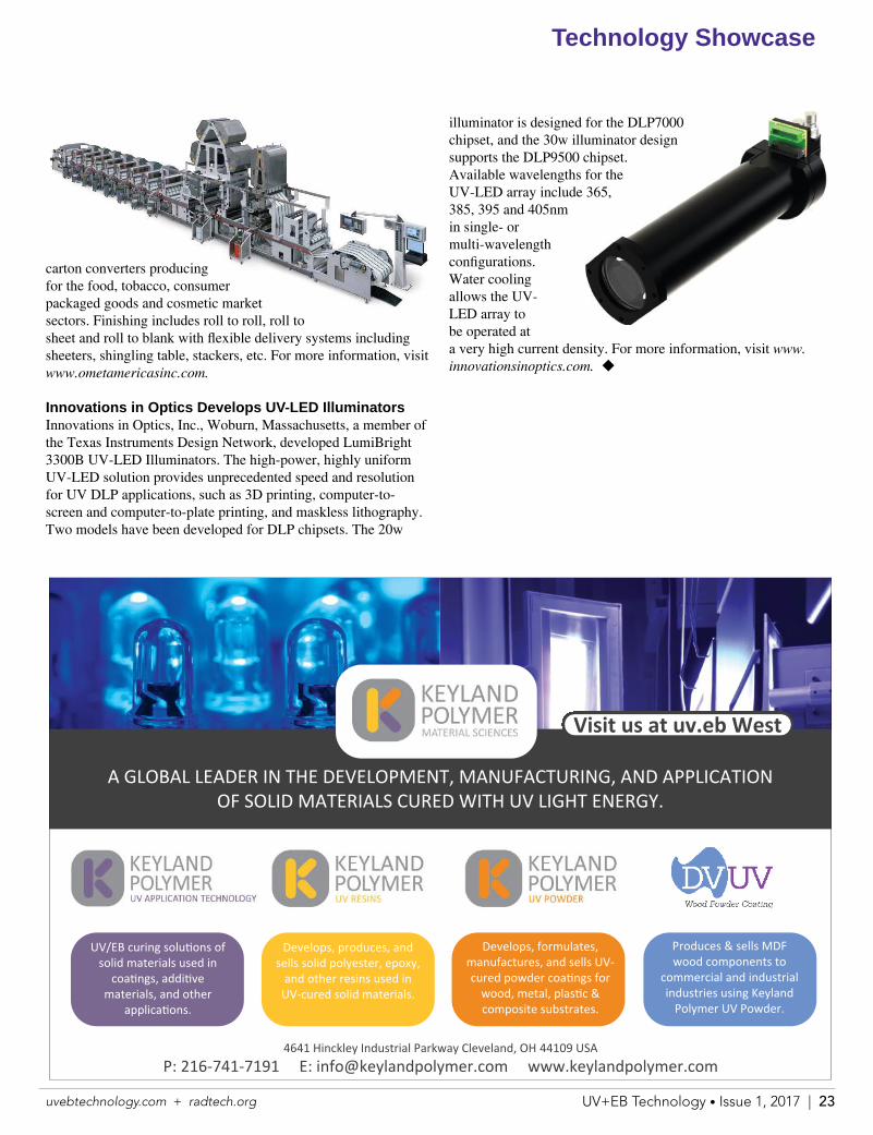
Innovations in Optics Develops UV-LED Illuminators Innovations in Optics, Inc., Woburn, Massachusetts, a member of the Texas Instruments Design Network, developed LumiBright 3300B UV-LED Illuminators. The high-power, highly uniform UV-LED solution provides unprecedented speed and resolution for UV DLP applications, such as 3D printing, computer-to-screen and computer-to-plate printing, and maskless lithography. Two models have been developed for DLP chipsets. The 20w
illuminator is designed for the DLP7000 chipset, and the 30w illuminator design supports the DLP9500 chipset. Available wavelengths for the UV-LED array include 365, 385, 395 and 405nm in single- or multi-wavelength configurations. Water cooling allows the UV-LED array to be operated at a very high current density. For more information, visit www.innovationsinoptics.com. u
A GLOBAL LEADER IN THE DEVELOPMENT, MANUFACTURING, AND APPLICATIONOF SOLID MATERIALS CURED WITH UV LIGHT ENERGY.
4641 Hinckley Industrial Parkway Cleveland, OH 44109 USAP: 216-741-7191 E: [email protected] www.keylandpolymer.com
UV/EB curing solu�ons ofsolid materials used incoa�ngs, addi�ve
materials, and otherapplica�ons.
Develops, produces, andsells solid polyester, epoxy,and other resins used inUV-cured solid materials.
Develops, formulates,manufactures, and sells UV-cured powder coa�ngs forwood, metal, plas�c &composite substrates.
Produces & sells MDFwood components to
commercial and industrialindustries using KeylandPolymer UV Powder.
Visit us at uv.eb West
24 | UV+EB Technology • Issue 1, 2017 uvebtechnology.com + radtech.org
By Michael R. Bonner, vice president of Engineering and Technology, Saint Clair Systems, Inc.
In modern coating operations, temperature-related variations can result in significant quality problems with film build, color match, surface finish, gloss, adhesion, etc. The first part of this series – shared in the
January edition of UV+EB Technology ENews – examined the intractable relationship between temperature and viscosity in modern coatings and compared the behavior of 100 percent solids UV cure coatings with more conventional solvent-borne and waterborne systems.
This article examines the two most common application processes: spraying and rolling. It also explores how modern temperature control systems can be used to turn temperature into a tool that can be used to control the outcomes of these processes.
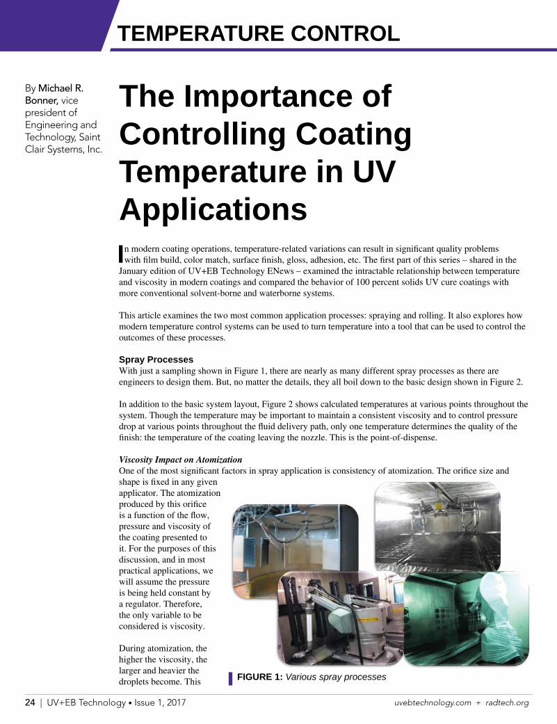
Spray ProcessesWith just a sampling shown in Figure 1, there are nearly as many different spray processes as there are engineers to design them. But, no matter the details, they all boil down to the basic design shown in Figure 2.
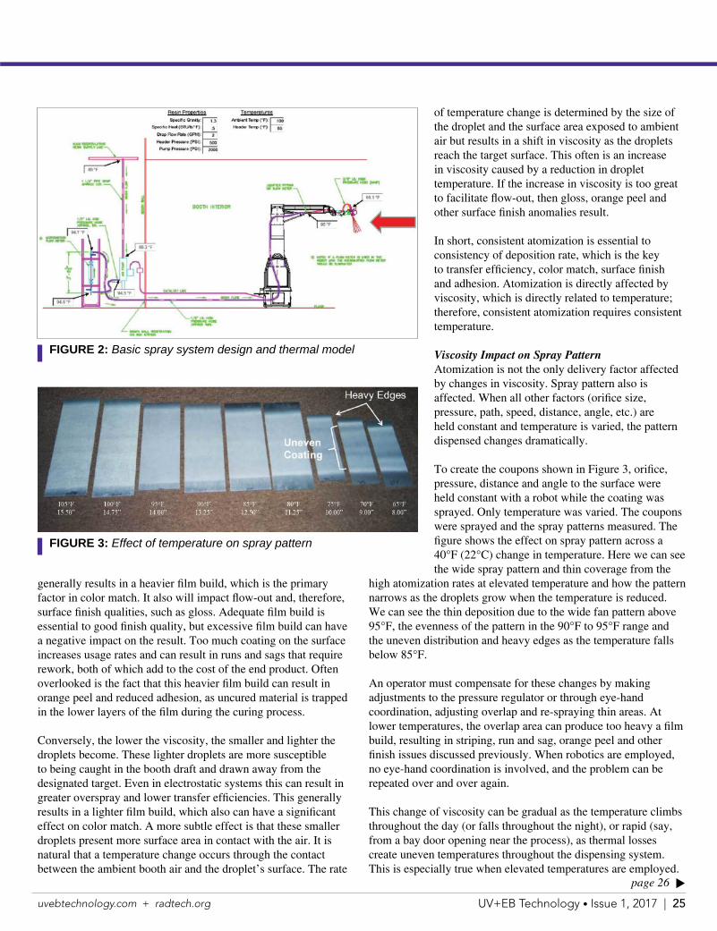
In addition to the basic system layout, Figure 2 shows calculated temperatures at various points throughout the system. Though the temperature may be important to maintain a consistent viscosity and to control pressure drop at various points throughout the fluid delivery path, only one temperature determines the quality of the finish: the temperature of the coating leaving the nozzle. This is the point-of-dispense.
Viscosity Impact on AtomizationOne of the most significant factors in spray application is consistency of atomization. The orifice size and shape is fixed in any given applicator. The atomization produced by this orifice is a function of the flow, pressure and viscosity of the coating presented to it. For the purposes of this discussion, and in most practical applications, we will assume the pressure is being held constant by a regulator. Therefore, the only variable to be considered is viscosity.
During atomization, the higher the viscosity, the larger and heavier the droplets become. This
The Importance of Controlling Coating Temperature in UV Applications
FIGURE 1: Various spray processes
TEMPERATURE CONTROL
uvebtechnology.com + radtech.org UV+EB Technology • Issue 1, 2017 | 25
page 26 u
generally results in a heavier film build, which is the primary factor in color match. It also will impact flow-out and, therefore, surface finish qualities, such as gloss. Adequate film build is essential to good finish quality, but excessive film build can have a negative impact on the result. Too much coating on the surface increases usage rates and can result in runs and sags that require rework, both of which add to the cost of the end product. Often overlooked is the fact that this heavier film build can result in orange peel and reduced adhesion, as uncured material is trapped in the lower layers of the film during the curing process.
Conversely, the lower the viscosity, the smaller and lighter the droplets become. These lighter droplets are more susceptible to being caught in the booth draft and drawn away from the designated target. Even in electrostatic systems this can result in greater overspray and lower transfer efficiencies. This generally results in a lighter film build, which also can have a significant effect on color match. A more subtle effect is that these smaller droplets present more surface area in contact with the air. It is natural that a temperature change occurs through the contact between the ambient booth air and the droplet’s surface. The rate
of temperature change is determined by the size of the droplet and the surface area exposed to ambient air but results in a shift in viscosity as the droplets reach the target surface. This often is an increase in viscosity caused by a reduction in droplet temperature. If the increase in viscosity is too great to facilitate flow-out, then gloss, orange peel and other surface finish anomalies result.
In short, consistent atomization is essential to consistency of deposition rate, which is the key to transfer efficiency, color match, surface finish and adhesion. Atomization is directly affected by viscosity, which is directly related to temperature; therefore, consistent atomization requires consistent temperature.
Viscosity Impact on Spray PatternAtomization is not the only delivery factor affected by changes in viscosity. Spray pattern also is affected. When all other factors (orifice size, pressure, path, speed, distance, angle, etc.) are held constant and temperature is varied, the pattern dispensed changes dramatically.
To create the coupons shown in Figure 3, orifice, pressure, distance and angle to the surface were held constant with a robot while the coating was sprayed. Only temperature was varied. The coupons were sprayed and the spray patterns measured. The figure shows the effect on spray pattern across a 40°F (22°C) change in temperature. Here we can see the wide spray pattern and thin coverage from the
high atomization rates at elevated temperature and how the pattern narrows as the droplets grow when the temperature is reduced. We can see the thin deposition due to the wide fan pattern above 95°F, the evenness of the pattern in the 90°F to 95°F range and the uneven distribution and heavy edges as the temperature falls below 85°F.
An operator must compensate for these changes by making adjustments to the pressure regulator or through eye-hand coordination, adjusting overlap and re-spraying thin areas. At lower temperatures, the overlap area can produce too heavy a film build, resulting in striping, run and sag, orange peel and other finish issues discussed previously. When robotics are employed, no eye-hand coordination is involved, and the problem can be repeated over and over again.
This change of viscosity can be gradual as the temperature climbs throughout the day (or falls throughout the night), or rapid (say, from a bay door opening near the process), as thermal losses create uneven temperatures throughout the dispensing system. This is especially true when elevated temperatures are employed.
FIGURE 2: Basic spray system design and thermal model
FIGURE 3: Effect of temperature on spray pattern
26 | UV+EB Technology • Issue 1, 2017 uvebtechnology.com + radtech.org
t page 25
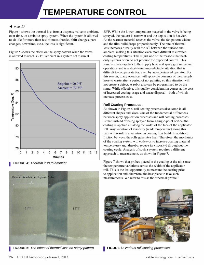
Figure 4 shows the thermal loss from a dispense valve to ambient, over time, on a robotic spray system. When the system is allowed to sit idle for more than few minutes (breaks, shift changes, part changes, downtime, etc.), the loss is significant.
Figure 5 shows the effect on the spray pattern when the valve is allowed to reach a 71°F ambient in a system set to run at
85°F. While the lower-temperature material in the valve is being sprayed, the pattern is narrower and the deposition is heavier. As the warmer material reaches the valve, the fan pattern widens and the film-build drops proportionately. The rate of thermal loss increases directly with the ∆T between the surface and ambient, making this situation even more difficult at elevated coating temperatures. This is just one of the reasons that heat-only systems often do not produce the expected control. This same scenario applies to the supply hose and spray gun in manual operations and is a short-term, unpredictable situation that is difficult to compensate for, even by an experienced operator. For this reason, many operators will spray the contents of their supply hose to waste after a period of not painting so this situation will not create a defect. A robot also can be programmed to do the same. While effective, this quality consideration comes at the cost of increased coating usage and waste disposal – both of which increase process cost.
Roll Coating ProcessesAs shown in Figure 6, roll coating processes also come in all different shapes and sizes. One of the fundamental differences between spray application processes and roll coating processes is that, instead of being sprayed from a single-point orifice, the coating is applied all along the width of the face of the applicator roll. Any variation of viscosity (read: temperature) along this path will result in a variation in coating film build. In addition, friction between the rolls generates heat. Therefore, the mechanics of the coating system will endeavor to increase coating material temperature (and, thereby, reduce its viscosity) throughout the coating cycle. Analysis of such a system requires a different approach to measurement, as shown in Figure 7.
Figure 7 shows that probes placed in the coating at the nip sense the temperature variations across the width of the applicator roll. This is the last opportunity to measure the coating prior to application and, therefore, the best place to take such measurements. We refer to this as the “thermal profile.”
FIGURE 4: Thermal loss to ambient
FIGURE 5: The effect of thermal loss on spray pattern FIGURE 6: Various roll coating processes
TEMPERATURE CONTROL

uvebtechnology.com + radtech.org UV+EB Technology • Issue 1, 2017 | 27
page 28 u
The heating phenomenon is clearly demonstrated in Figure 8, which shows the temperature profile of a roll coating system without temperature control over an hour’s time. Plotted are ambient temperature, drum temperature and the temperature at eight points across the width of the roll. This graph reveals interesting details about the roll coating process. The first is that the process temperature rises 10°F, while ambient rises just 5°F, over the course of this hour. This shows that, because of friction-generated heat, controlling the ambient temperature in the booth cannot accurately control the temperature of the coating.
Previously, we showed the impact temperature has on coating viscosity. Furthermore, the total 4s processing range (26s ±2s) translates to a 5°F window from 80°F to 85°F. Even though the coating was at the 80°F lower limit when the process started, the friction in the system moved the temperature twice the allowable tolerance in just one hour, which will require making other adjustments to compensate for the change in viscosity.
An interesting note from Figure 8 is that the eight points across the face of the pickup roller show a significant variation in temperature. This is depicted more clearly in the “Thermal Profile” display in Figure 9. What we cannot see from this graph is that this uncorrected profile displays continuous variation. What we can see from this graph is that this variation exceeds 7°F at times. This means that the total allowable tolerance is exceeded by variations across the width of the strip. The result is that portions of the coating across the width will always be outside of the viscosity specification. As shown, this can be a sharp change that cannot be compensated for by simply varying the nip pressure from side to side. To assure adequate film build at all points across the width of the strip under these conditions, it often is necessary to increase the total film build, laying down more material than is actually required in some areas to ensure we get the minimum in others.
This effect on film build is demonstrated in Figure 10. Here we can see that the areas of higher temperature result in lower viscosity, which produces a thinner film build, whereas the cooler areas result in higher viscosity and produce a heavier film.
The goal then must be to reduce variations in viscosity as the coating is being applied to the substrate. Unfortunately, identifying and correcting the factors that create viscosity variation at the point of use can be complex and must be treated on a case-by-case basis. It is clear however, this can only be accomplished through the careful manipulation of the flow dynamics in the system as well as the supply temperature of the coating. Figure 11 shows this same system after correction of the thermal profile and the impact on the film build. Here we see that the total temperature variation across the width of the strip has been reduced to about 1°F. This translates to a total edge-to-edge viscosity variation of about 0.8s, or just 20 percent of the total operating window.
Point of Use Temperature ControlIn each of these cases, it is clear that the solution to the question of how to stabilize the process lies with controlling the temperature of the coating at the point of application. Though the approach for each is unique, the end result is the same – stabilizing the temperature stabilizes the viscosity and helps to bring the process under control.
It is equally important to accurately control the temperature at the optimal value. Often, with modern UV coatings, that optimal value is exceeded by the ambient temperature. In many cases and in many climates, it is necessary to heat the coating during the cool morning hours and cool it through the warmth of the afternoon. Seasonal temperature variations are even more extreme, but present similar requirements. We also have shown
FIGURE 7: Measuring temperatures in a roll coating system
FIGURE 8: The effect of process friction on temperature1

28 | UV+EB Technology • Issue 1, 2017 uvebtechnology.com + radtech.org
t page 27
that many systems generate friction as a part of the delivery and application process. The friction manifests itself as heat, which must be removed by the temperature control system. In virtually all modern coating applications, a system capable of both heating and cooling – and of switching seamlessly between the two – is essential.
Recent advances in both methodology and thermal transfer devices make temperature a tool that can be utilized to protect the integrity of the coating and optimize the performance of both the coating and the application process. These new and more efficient means move temperature control from the bulk supply at the beginning of the process to the point of application, where it can have a more positive effect on the performance of the coating process. This adds another important parameter to the list of those that combine to control the process, and if the parameters of a proven “coating recipe” can be held constant, the resulting application outcome will be consistent and repeatable.
ConclusionThough modern UV coatings may be very different chemically from their conventional waterborne and solvent-borne counterparts, the methods employed to dispense and apply them – and their behaviors within those systems – are very similar. This is especially advantageous where modern coating formulations can be substituted for older versions to gain significant performance and/or ecological benefits without incurring major rework, downtime and cost in the conversion. In each case, temperature variations result in viscosity variations that can undermine the advantages of converting. In fact, as shown, the modern coating formulations often are more temperature sensitive than their conventional counterparts.
Modern temperature control systems use innovative approaches and devices to eliminate temperature-based viscosity variations at the point of application and achieve consistent, repeatable performance, independent of changes in ambient temperature and/or processing conditions. This turns temperature from an adversary working against the process into a tool that can be utilized in conjunction with other tools (pressure regulators, speed controls and the like) to assure the coating process outcomes are completely predictable and advance the goals and objectives of the business. u
Bibliography1. The Effect of Process Friction on Temperature data provided courtesy of Alsco Metals Corporation, Roxboro, North Carolina.2. Roll Coating Thermal Profile data provided courtesy of Alsco Metals Corporation, Ashville, Ohio, utilizing Saint Clair Systems’ Profile Analysis and Correction System.
Michael R. Bonner is the vice president of engineering and technology for Saint Clair Systems, Inc., a leading supplier of process temperature control equipment for industrial fluid processing systems. For more information, call 586.336.0700 or visit www.saintclairsystems.com.
FIGURE 9: Thermal profile variation2
FIGURE 10: Uncorrected profile and effect on film build
FIGURE 11: Corrected profile and effect on film build
TEMPERATURE CONTROL

uvebtechnology.com + radtech.org UV+EB Technology • Issue 1, 2017 | 29
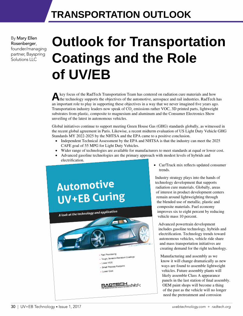
30 | UV+EB Technology • Issue 1, 2017 uvebtechnology.com + radtech.org
A key focus of the RadTech Transportation Team has centered on radiation cure materials and how the technology supports the objectives of the automotive, aerospace and rail industries. RadTech has
an important role to play in supporting these objectives in a way that we never imagined five years ago. Transportation industry leaders now speak of CO2 emissions rather VOC, 3D printed parts, lightweight substrates from plastic, composite to magnesium and aluminum and the Consumer Electronics Show unveiling of the latest in autonomous vehicles.
Global initiatives continue to support meeting Green House Gas (GHG) standards globally, as witnessed in the recent global agreement in Paris. Likewise, a recent midterm evaluation of US Light Duty Vehicle GHG Standards MY 2022-2025 by the NHTSA and the EPA came to a positive conclusion.• Independent Technical Assessment by the EPA and NHTSA is that the industry can meet the 2025
CAFE goal of 55 MPG for Light Duty Vehicles.• Wider range of technologies are available for manufacturers to meet standards at equal or lower cost.• Advanced gasoline technologies are the primary approach with modest levels of hybrids and
electrification.• Car/Truck mix reflects updated consumer
trends.
Industry strategy plays into the hands of technology development that supports radiation cure materials. Globally, areas of interest in product development centers remain around lightweighting through the blended use of metallic, plastic and composite materials. Fuel economy improves six to eight percent by reducing vehicle mass 10 percent.
Advanced powertrain development includes gasoline technology, hybrids and electrification. Technology trends toward autonomous vehicles, vehicle ride share and mass transportation initiatives are creating demand for the right technology.
Manufacturing and assembly as we know it will change dramatically as new ways are found to assemble lightweight vehicles. Future assembly plants will likely assemble Class A appearance panels in the last station of final assembly. OEM paint shops will become a thing of the past as the vehicle will no longer need the pretreatment and corrosion
Outlook for Transportation Coatings and the Role of UV/EB
By Mary Ellen Rosenberger, founder/managing partner, Bayspring Solutions LLC
TRANSPORTATION OUTLOOK
uvebtechnology.com + radtech.org UV+EB Technology • Issue 1, 2017 | 31
protection required of ferrous metal substrates. Painting of parts will become the job of Tier 1 suppliers that deliver parts line side. Lightweighting of the vehicle will shift to a space frame design, lightweight components and flat panel designs held together by adhesives and protected with space-age sealer.
Development of radiation-cured materials that support heat sensitive substrates, lightweight glass alternatives and electronics are all needed to support the vehicles of the future. Sealers and adhesives will be used in volumes that support new vehicle substrate designs.
3D printing has altered vehicle development time to months rather than years. Complex parts and small-volume replacement parts are more easily printed than molded. Material science is urgently needed to support automotive durability demands for 3D printed materials. Automotive innovation centers have teams devoted to 3D printing as the technology becomes the next production reality.
To say that the tail is wagging the dog is an understatement. New developments and innovation will reshape the transportation industry from top to bottom. We see new players all around us, from Tesla to Faraday Future. However, do not think for a moment that existing OEMs are not pulling their weight in the quest to meet global demand for improved fuel economy and reduced GHG emissions. We all play a role in developing products for these new times.
RadTech has formed a team for a second year to support the SAE (Society of Automotive Engineers) World Congress 2017, to be held April 4-6, 2017, in Detroit, Michigan. Chaired by Dr. Christopher Seubert – Ford Paint, Innovation Center (a new member to the RadTech Board), some exciting papers will be presented in session M401 – “UV EB Leading the Way for Automotive.” Amongst the topics covered will include lightweighting, hardcoats for glass, interior/exterior trim coatings, 3D Materials and “Paint Shop of the Future – Facility Designs.”
Future work for the RadTech Transportation Group will take on a more strategic role in developing ideas and products that support future industry goals. These could include the following:
1. Transportation themes• Meeting Future GHG Standards – Lightweight Vehicles/
Powertrain Technologies
New VenueExpanded Exhibit Space
Sponsorship Opportunities
Visit With Suppliers To The Coatings Industry On Our Trade Show Floor
For Registration, Hotel and Program/Show Information Go To Our Website:
www.easterncoatingsshow.comFor Specifi c Questions Please Contact Us:
Email: [email protected] Hosted By: Eastern Coatings Federation, Inc.
MAY 15 TO MAY 17, 2017 HARRAH’S RESORT ATLANTIC CITY, NEW JERSEY
To say that the tail is wagging the dog is an understatement. New developments and innovation will reshape the transportation industry from top to bottom.
page 32 u

32 | UV+EB Technology • Issue 1, 2017 uvebtechnology.com + radtech.org
t page 31
Abrasion Resistant Clears for Parts Gaskets
Plastic Wheel Cover Color & Clear
Anti-Scratch UV Post-Cure Films
Windshield Repair Products
Current Uses of UV+EB Cure TechnologyAutomotive manufacturers are constantly searching for ways to make things faster, better and cheaper. UV+EB Curing is significantly faster than traditional thermal/ambient processes, producing fewer defects by delivering final properties immediately, resulting in a smaller process footprint and a lower cost per part.
Coil Terminators
Potting Compounds
Printed Circuit Conformal Coatings
Printed Circuit Solder Masks
Interior Mar/Chemical Resistant High-Gloss Blacks
Logos on Glass
Topcoats for RV, Van “Wood” Components
Metalized Primer for PVD Parts
Anti-Scratch Tail-Light Coatings
Dashboard Screen Printing
SMC Sealer
Mirror Adhesives
Primer Sealers
Windshield Black-Out
Hardcoat for Forward Lighting Body Side Molding
Clear Coats
Component Marking Inks
Tacking Adhesives
Lens Reflector Adhesives
Battery Labels
Oil Filter Housings
Fleet Markings
Airbag Sealant Cartridges
• Autonomous Vehicles• Electronics
» Mass Transportation – Vehicle Ride Share2. Base Technology
• Material Science• 3D Printing – Vehicle Development and Manufactured
Parts• Electrification• Cyber Security/Information Technology.
Development of radiation-cured materials that support heat-sensitive substrates, lightweight glass alternatives and electronics are all needed to support the vehicles of the future.
RadTech work group opportunities presented at the Austin, Texas, Transportation Group meeting will be developed further with Dr. Christopher Seubert at the upcoming uv.eb West 2017 event in San Francisco, California. These opportunities include the following
• Lightweighting • 3D Printing – Functional Materials• Assembly Plant of the Future• Automotive Durability Standards
In conclusion, technology opportunities that will shape the future for the transportation industry are being developed in research and development centers around the world. RadTech is poised to support the transportation industry locally and globally. Current development roadblocks will be resolved by commercial solutions very soon. u
Images in this article and on the magazine cover are from RadTech’s Guide to the Current Automative Uses for UV/EB. For more information on this resource, contact RadTech International North America at [email protected].
TRANSPORTATION OUTLOOK
Internal page view of RadTech’s Guide to Current Automotive Uses for UV/EB.
TM
34 | UV+EB Technology • Issue 1, 2017 uvebtechnology.com + radtech.org
Abstract
This paper will explain the basics of ultraviolet (UV) curing, including peak irradiance (Watts/cm2), energy density (Joules/cm2), spectral wavelength (nm) and total power (Watts), as well as the fundamental
differences between electrode, microwave and UV LED curing systems. It will further highlight the benefits of using UV LED technology, the trends driving its adoption into an increasing range of production technologies and, more importantly, its growing viability in automotive and transportation applications.
IntroductionThe automotive and transportation industry face several design, engineering and manufacturing challenges over the coming years. Many of these involve preparing for the Corporate Average Fuel Economy (CAFE) standards requiring manufacturers to achieve a production-weighted 54.5 miles per gallon by 2025. Others have to do with better global stewardship, driving further reductions in waste and energy consumption at assembly and supplier plants. Finally, a constantly changing worker demographic and high-tech skills shortage will likely mean even more automation and process control throughout global production facilities. For each of these challenges, many new manufacturing processes will likely need to be developed.
While conventional UV curing through the use of microwave and arc lamps has been used in automotive and transportation production processes for decades, UV LED curing is relatively new and has not gained much traction. In other markets, however, UV LED technology is much more mainstream, as significant equipment and formulation advances enable the technology to quickly penetrate a growing range of applications. This is primarily driven by the fact that UV LED technology offers numerous performance, operating and environmental benefits and is considered an enabling technology that lends its use to curing inks, adhesives and coatings on a greater range of heat-sensitive materials while delivering overall process and quality control. As a result, the transformational nature of UV LED curing is something that should be explored and evaluated for its production use viability as automotive and transportation companies strive to meet various manufacturing challenges over the coming decade.
In an effort to introduce the automotive and transportation industry to the merits of UV LED curing, this paper will begin by explaining the basics of curing from an equipment perspective.
Industrial Sources of UV CuringIndustrial sources of UV energy have long included medium-pressure mercury arc and microwave-powered lamps and, more recently, light emitting diodes (LEDs). All three technologies are used to crosslink inks, coatings and adhesives in a wide range of manufacturing processes. Both arc and microwave curing technologies rely on the vaporization of mercury within a sealed quartz tube containing an inert gas mixture. The physics of mercury are such that it emits ultraviolet light when vaporized. Electrodeless lamps employ microwaves to vaporize the mercury, whereas electrode lamps harness a high-voltage arc struck between two electrodes to achieve the same result. When the mercury is vaporized into an extremely high-temperature plasma gas, it emits a spectral output across the UVA, UVB, UVC and UVV bands that can be manipulated a small degree by introducing metallic additives to the inside of the lamps. Lamps with added metals are
By Jennifer Heathcote, regional sales manager, Phoseon Technology
The Growing Viability of UV LED for Automotive and Transportation Applications
UV LED

uvebtechnology.com + radtech.org UV+EB Technology • Issue 1, 2017 | 35
Segment Innovators EarlyAdopters
EarlyMajority
LateMajority
Digital Inkjet Accomplished Accomplished Accomplished In Progress
Spot Curing Accomplished Accomplished Accomplished In Progress
Screen – Graphics Accomplished Accomplished In Progress
Offset - Sheet Fed Accomplished Accomplished In Progress
Flexo - Narrow Web Accomplished Accomplished In Progress
3D Manufacturing Accomplished Accomplished
Structural Bonding Accomplished Some Installs
Coatings – Wide Web Exploring Some Installs
Flexo - Wide Web Exploring
Offset – Web Exploring
Screen – IMD Exploring
Coatings – 3D Parts
page 36 u
typically referred to as doped, additive or metal halide. Most ink, adhesive and coating formulations over the past several decades have been formulated to match the output of standard mercury lamps as well as iron and gallium doped lamps. When the formulations are exposed to the ultraviolet energy, they are crosslinked into a photopolymer.
UV LEDs, on the other hand, are solid-state semiconductors. They contain no moving parts or mercury plasma gas and operate at temperatures that are often less than 1/10 the operating temperatures of conventional lamps. When connected to a DC power source, an electric current flows through the semiconductors, dropping electrons into a state of lower energy as they travel from the negative to the positive side of each discrete LED. The energy differential is released from the device in the form of a relatively monochromatic spectral distribution.
Commercially, UV LED technology has significant market adoption with longer UVA wavelengths (365, 385, 395 and 405 nm), and development work in shorter UVB and UVC bands continues. While there is no UV LED source that directly mimics a conventional lamp, the longer wavelengths emitted by LEDs result in their spectral distribution being more similar to an iron or gallium lamp than a basic mercury lamp. The result is that UV LED wavelengths can penetrate deeper into the chemistry and produce better through-cure, particularly with opaque and pigmented formulations. For clear coatings, achieving a hard, scratch-resistant surface cure without yellowing has been the primary challenge for UV LEDs. This is because many coatings formulations rely on the shorter wavelengths emitted by broadband lamps for sufficient crosslinking at the surface, and current UVB and UVC LEDs do not yet satisfy curing requirements in these shorter wavelengths. Nevertheless, higher irradiances and adjustments to the formulations often have been found to resolve these issues. For the others, ongoing development work is being done to attempt to close the gap.
Both microwave and arc lamps are widely used in today’s manufacturing processes, as they have been for decades. By comparison, UV LED lamps represent a much smaller but growing proportion of the installed base, with the first devices appearing on the market in the early 2000s. For many years, UV LED curing systems were of relatively low power and had limited commercial use. But – after more than 10 years of continued advancements in the areas of power output, efficiency, reliability, operation, integration, formulation and production economics – the technology is being utilized across an ever growing list of applications. The exciting evolution of UV LED technology continues, presenting numerous opportunities for manufacturing processes – including many of interest to the automotive and transportation industries.
UV Curing Market EvolutionThe development efforts for industrial curing utilizing arc lamps (1940s), microwave lamps (1970s) and UV LEDs (2000s) each have their unique beginnings. Regardless of how rudimentary or seemingly inconsequential those beginnings may have appeared at the time, each formed building blocks that eventually made much more challenging feats possible. In much the same way, UV LED curing continues to evolve and prove its effectiveness in increasingly more demanding scenarios. As a result, it is reasonable to expect the use of UV LED technology in production environments to follow a similar development and adoption path over time.
The earliest commercial successes for UV LED, occurring between 2004 and 2010, were rather limited in scale and scope when measured against the much larger and significantly more established installation base of conventional UV curing. Many of the first UV LED installations involved spot-curing adhesives and digital inkjet inks. The applications predominantly dealt with slower line speeds or longer dwell times and involved installations that were conducive to the low-power emitting sources being
positioned very close to the cure surface.
For those closely tracking the progress of early UV LED curing developments, it became clear rather quickly that the technology eventually would be good enough to fully capture the early adopter markets and later expand into other markets. It was just a matter of time, effort and funding, as well as establishing sufficient demand amongst end users. For those on the outside, however, it was equally easy to discount the impact that any UV LED successes in these isolated markets would have on all the other UV curing markets. To most, the fact that early UV LED sources were simply not as good at curing existing chemistry as conventional UV sources drove many overarching conclusions that the technology’s impact ultimately would be restricted. It is important to note, however, that it is all too easy FIGURE 1: General state of UV LED adoption across a range of UV
curing applications
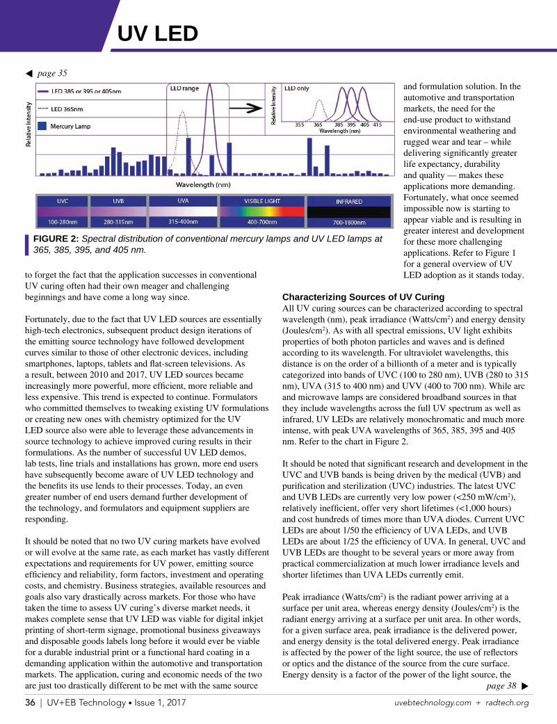
36 | UV+EB Technology • Issue 1, 2017 uvebtechnology.com + radtech.org
t page 35
page 38 u
to forget the fact that the application successes in conventional UV curing often had their own meager and challenging beginnings and have come a long way since.
Fortunately, due to the fact that UV LED sources are essentially high-tech electronics, subsequent product design iterations of the emitting source technology have followed development curves similar to those of other electronic devices, including smartphones, laptops, tablets and flat-screen televisions. As a result, between 2010 and 2017, UV LED sources became increasingly more powerful, more efficient, more reliable and less expensive. This trend is expected to continue. Formulators who committed themselves to tweaking existing UV formulations or creating new ones with chemistry optimized for the UV LED source also were able to leverage these advancements in source technology to achieve improved curing results in their formulations. As the number of successful UV LED demos, lab tests, line trials and installations has grown, more end users have subsequently become aware of UV LED technology and the benefits its use lends to their processes. Today, an even greater number of end users demand further development of the technology, and formulators and equipment suppliers are responding.
It should be noted that no two UV curing markets have evolved or will evolve at the same rate, as each market has vastly different expectations and requirements for UV power, emitting source efficiency and reliability, form factors, investment and operating costs, and chemistry. Business strategies, available resources and goals also vary drastically across markets. For those who have taken the time to assess UV curing’s diverse market needs, it makes complete sense that UV LED was viable for digital inkjet printing of short-term signage, promotional business giveaways and disposable goods labels long before it would ever be viable for a durable industrial print or a functional hard coating in a demanding application within the automotive and transportation markets. The application, curing and economic needs of the two are just too drastically different to be met with the same source
and formulation solution. In the automotive and transportation markets, the need for the end-use product to withstand environmental weathering and rugged wear and tear – while delivering significantly greater life expectancy, durability and quality — makes these applications more demanding. Fortunately, what once seemed impossible now is starting to appear viable and is resulting in greater interest and development for these more challenging applications. Refer to Figure 1 for a general overview of UV LED adoption as it stands today.
Characterizing Sources of UV CuringAll UV curing sources can be characterized according to spectral wavelength (nm), peak irradiance (Watts/cm2) and energy density (Joules/cm2). As with all spectral emissions, UV light exhibits properties of both photon particles and waves and is defined according to its wavelength. For ultraviolet wavelengths, this distance is on the order of a billionth of a meter and is typically categorized into bands of UVC (100 to 280 nm), UVB (280 to 315 nm), UVA (315 to 400 nm) and UVV (400 to 700 nm). While arc and microwave lamps are considered broadband sources in that they include wavelengths across the full UV spectrum as well as infrared, UV LEDs are relatively monochromatic and much more intense, with peak UVA wavelengths of 365, 385, 395 and 405 nm. Refer to the chart in Figure 2.
It should be noted that significant research and development in the UVC and UVB bands is being driven by the medical (UVB) and purification and sterilization (UVC) industries. The latest UVC and UVB LEDs are currently very low power (<250 mW/cm2), relatively inefficient, offer very short lifetimes (<1,000 hours) and cost hundreds of times more than UVA diodes. Current UVC LEDs are about 1/50 the efficiency of UVA LEDs, and UVB LEDs are about 1/25 the efficiency of UVA. In general, UVC and UVB LEDs are thought to be several years or more away from practical commercialization at much lower irradiance levels and shorter lifetimes than UVA LEDs currently emit.
Peak irradiance (Watts/cm2) is the radiant power arriving at a surface per unit area, whereas energy density (Joules/cm2) is the radiant energy arriving at a surface per unit area. In other words, for a given surface area, peak irradiance is the delivered power, and energy density is the total delivered energy. Peak irradiance is affected by the power of the light source, the use of reflectors or optics and the distance of the source from the cure surface. Energy density is a factor of the power of the light source, the
FIGURE 2: Spectral distribution of conventional mercury lamps and UV LED lamps at 365, 385, 395, and 405 nm.
UV LED

THE SOLUTION IN ENERGY CURING
Products are engineered to support changing market needs:
• Cross contamination free• Toluene free (HAP free)• Consistency in quality• BPA-free systems• High purity• Low residuals• Low extractables• High refractive index• Tin-free oligomers• Captive EO/PO capability
As a member of the American Chemistry Council, we are committed to the principles of Responsible Care.
Miwon Specialty Chemical Co., Ltd. is a world-class producer of specialty acrylate and methacrylate monomers and oligomers.
Miwon maintains a global presence – in Asia, North America and Europe – with full-scale production facilities, regional technical support laboratories, regional customer sales/supply support offices and local warehouses.
We are a key raw materials supplier to the inks, coatings, adhesives and electronics industries. As manufacturing raw materials for UV and EB curing is our core business, we offer one of the broadest product lines for formulators utilizing this advanced and environmentally friendly technology.
Phone: 484-872-8711Fax: 484-872-8717
Miwon Specialty Chemical Co., Ltd.Miwon North America696 W. Lincoln HighwayExton, PA 19341

38 | UV+EB Technology • Issue 1, 2017 uvebtechnology.com + radtech.org
t page 36
number of UV sources and the exposure time. Understanding and managing spectral output, irradiance and energy density is essential for formulating UV curable materials, selecting the correct UV sources for a production line and ensuring the desired production speeds and cure results are achieved.
Conventional arc lamps typically emit in the range of 1 to 3 Watts/cm2 while microwave lamps generally emit as much as 5 Watts/cm2. UV LED curing systems, on the other hand, emit up to 16 Watts/cm2 for air-cooled heads and 24 Watts/cm2 for liquid-cooled heads. While the irradiance of UV LED systems is significantly greater than that of arc and microwave systems, the tradeoff is that the output is currently restricted to longer UVA wavelengths. It is important to note that, while energy density increases with increases in irradiance for a given UV LED source, a high irradiance specified by a manufacturer does not necessarily guarantee a high energy density. Energy density depends on the construction and configuration of the UV LED curing system. While a minimum threshold irradiance is necessary for chemistry cross-linking to occur, a higher energy density at or above the required minimum irradiance threshold is what delivers sufficient cure at faster production speeds. When evaluating different models from the same supplier or systems from different suppliers, it is important to understand both the irradiance and the energy density and how the two affect cure and line speed.
The fourth characteristic of UV LED sources is total power (Watts). Total power is measured by an integrating sphere and is considered to be the most accurate method of measuring UV LED sources within a given family of products and across generations of a given product. The process involves directing UV emissions from the lamp head such that they illuminate the internal surface of a large sphere coated with a highly uniform, diffuse, white material. The output of the UV LED source is reflected multiple times off the inside surface of the sphere and distributed equally to all points, allowing a small sensor to accurately
measure total power independent of the source light direction. Integrating spheres are reliable, repeatable and precise tools used to evaluate the output of a UV LED curing lamp; however, the measurements from the devices are not practical for use in the field and currently are not used to determine irradiance and energy density. Irradiance and energy density are instead measured with radiometers.
UV LED Uniformity and Output ProfilesWhen building a UV LED curing system, numerous raw or native LEDs are typically arranged in a single line or matrix configuration. The UV output from each discrete LED follows Lambertian characteristics in that the perceived brightness remains constant as the viewing angle changes. The output from each LED is divergent and, if the matrix of LEDs is configured correctly, blends uniformly with the output of neighboring LEDs. The uniformity of the UV rays on a given plane always improves as the distance of the plane from the matrix increases.
For most applications, it is critical to have uniformity of output along the length of the LED curing source as well as between mating sources. When individual UV LED sources are seamlessly mated end-to-end, this is referred to as scaling the heads. It should be noted that not all commercially available systems are scalable, nor do they all offer the same uniformity characteristics. It is recommended that uniformity for a given product be discussed with the UV LED supplier. Sources that exhibit better uniformity along the length of the head, as well as between scaled heads, deliver better quality and consistency of cure across wider substrates or parts. In all cases, uniformity improves as the distance between the matrix and the substrate or part increases.
Uniformity of UV LED heads and scaled heads is illustrated in Figures 3 and 4. Irradiance readings were taken along the length of a 150-mm head and along the length of two scaled heads. The red trend line measurements were taken with the radiometer at a
FIGURE 3: Illustration of Uniformity of Peak Irradiance along the Length of a UV LED Source.
FIGURE 4: Illustration of Uniformity of Peak Irradiance Along Length of Two Scaled UV LED Sources.
UV LED
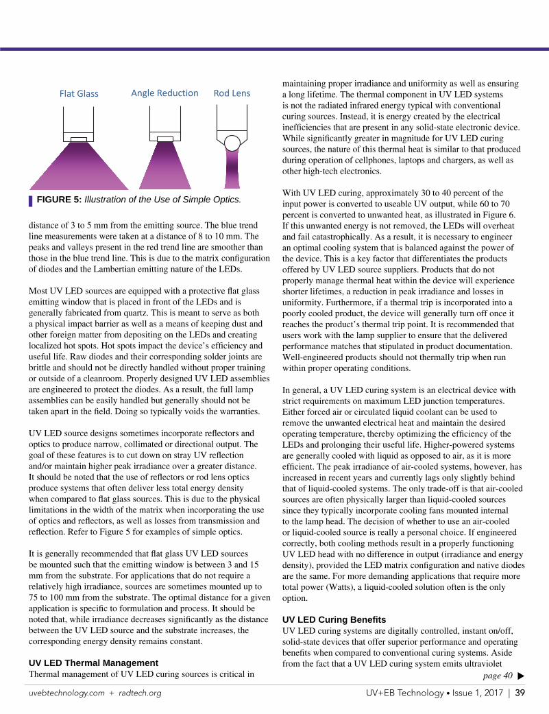
uvebtechnology.com + radtech.org UV+EB Technology • Issue 1, 2017 | 39
distance of 3 to 5 mm from the emitting source. The blue trend line measurements were taken at a distance of 8 to 10 mm. The peaks and valleys present in the red trend line are smoother than those in the blue trend line. This is due to the matrix configuration of diodes and the Lambertian emitting nature of the LEDs.
Most UV LED sources are equipped with a protective flat glass emitting window that is placed in front of the LEDs and is generally fabricated from quartz. This is meant to serve as both a physical impact barrier as well as a means of keeping dust and other foreign matter from depositing on the LEDs and creating localized hot spots. Hot spots impact the device’s efficiency and useful life. Raw diodes and their corresponding solder joints are brittle and should not be directly handled without proper training or outside of a cleanroom. Properly designed UV LED assemblies are engineered to protect the diodes. As a result, the full lamp assemblies can be easily handled but generally should not be taken apart in the field. Doing so typically voids the warranties.
UV LED source designs sometimes incorporate reflectors and optics to produce narrow, collimated or directional output. The goal of these features is to cut down on stray UV reflection and/or maintain higher peak irradiance over a greater distance. It should be noted that the use of reflectors or rod lens optics produce systems that often deliver less total energy density when compared to flat glass sources. This is due to the physical limitations in the width of the matrix when incorporating the use of optics and reflectors, as well as losses from transmission and reflection. Refer to Figure 5 for examples of simple optics.
It is generally recommended that flat glass UV LED sources be mounted such that the emitting window is between 3 and 15 mm from the substrate. For applications that do not require a relatively high irradiance, sources are sometimes mounted up to 75 to 100 mm from the substrate. The optimal distance for a given application is specific to formulation and process. It should be noted that, while irradiance decreases significantly as the distance between the UV LED source and the substrate increases, the corresponding energy density remains constant.
UV LED Thermal ManagementThermal management of UV LED curing sources is critical in
maintaining proper irradiance and uniformity as well as ensuring a long lifetime. The thermal component in UV LED systems is not the radiated infrared energy typical with conventional curing sources. Instead, it is energy created by the electrical inefficiencies that are present in any solid-state electronic device. While significantly greater in magnitude for UV LED curing sources, the nature of this thermal heat is similar to that produced during operation of cellphones, laptops and chargers, as well as other high-tech electronics.
With UV LED curing, approximately 30 to 40 percent of the input power is converted to useable UV output, while 60 to 70 percent is converted to unwanted heat, as illustrated in Figure 6. If this unwanted energy is not removed, the LEDs will overheat and fail catastrophically. As a result, it is necessary to engineer an optimal cooling system that is balanced against the power of the device. This is a key factor that differentiates the products offered by UV LED source suppliers. Products that do not properly manage thermal heat within the device will experience shorter lifetimes, a reduction in peak irradiance and losses in uniformity. Furthermore, if a thermal trip is incorporated into a poorly cooled product, the device will generally turn off once it reaches the product’s thermal trip point. It is recommended that users work with the lamp supplier to ensure that the delivered performance matches that stipulated in product documentation. Well-engineered products should not thermally trip when run within proper operating conditions.
In general, a UV LED curing system is an electrical device with strict requirements on maximum LED junction temperatures. Either forced air or circulated liquid coolant can be used to remove the unwanted electrical heat and maintain the desired operating temperature, thereby optimizing the efficiency of the LEDs and prolonging their useful life. Higher-powered systems are generally cooled with liquid as opposed to air, as it is more efficient. The peak irradiance of air-cooled systems, however, has increased in recent years and currently lags only slightly behind that of liquid-cooled systems. The only trade-off is that air-cooled sources are often physically larger than liquid-cooled sources since they typically incorporate cooling fans mounted internal to the lamp head. The decision of whether to use an air-cooled or liquid-cooled source is really a personal choice. If engineered correctly, both cooling methods result in a properly functioning UV LED head with no difference in output (irradiance and energy density), provided the LED matrix configuration and native diodes are the same. For more demanding applications that require more total power (Watts), a liquid-cooled solution often is the only option.
UV LED Curing BenefitsUV LED curing systems are digitally controlled, instant on/off, solid-state devices that offer superior performance and operating benefits when compared to conventional curing systems. Aside from the fact that a UV LED curing system emits ultraviolet
lat lass ngle eduction od ens
FIGURE 5: Illustration of the Use of Simple Optics.
page 40 u

40 | UV+EB Technology • Issue 1, 2017 uvebtechnology.com + radtech.org
energy, the device has more in common with a typical smartphone than it does with an arc or microwave curing system. Because UV LED systems emit longer UVA wavelengths and no UVC or UVB, LED systems are better at penetrating more heavily pigmented and opaque formulations. The lack of UVB and UVC means that no ozone is produced during operation. This eliminates the need for exhaust and conditioned plant make-up air. No infrared energy also means that UV LED curing systems work across a greater range of heat-sensitive substrates. It should be noted, however, that UV LED devices still represent a source of emitted energy (Watts), even if there is no infrared component. This energy can be converted to thermal heat on the substrate or part, albeit significantly less than that generated by conventional UV sources. Parking a UV LED head over a substrate or part for a prolonged period will heat the exposed materials. The exposed part or substrate temperature, as well as the time duration needed to cause damage to the part or substrate, varies depending on the material and the setup. The beauty of LEDs is that they are instant on/off. As a result, the UV source is cycled on/off as needed and interlocked to material-handling equipment so that if any production stops occur, the light immediately switches off and then back on as soon as the line starts again.
UV LED curing systems eliminate the spare parts and accessories typically associated with conventional curing systems. These include bulbs, reflectors, shutters, magnetrons, RF screens and exhaust ducting. Conventional bulbs typically last between 500 and 2,000 hours and begin degrading from the first second they are powered. Properly engineered UV LED systems, on the other hand, have demonstrated lifetimes between 20,000 and 60,000 hours with degradation of less than 15 to 20 percent of peak output over that period. Well engineered internal device monitoring often can make adjustments to the drive power as the lamps age, thereby compensating for any natural degradation. UV LED curing systems operate on DC power, as opposed to an AC transformer or ballast, and generally consume 50 to 75 percent
less energy when compared one to one with conventional systems. UV LED curing systems also eliminate mercury and ozone, as well as UVB and UVC wavelengths, all of which make for a safer operating environment. The only maintenance issues to note are keeping the emitting window, optics, reflectors and air filters clean, as well as maintaining the fill levels in the reservoirs of chillers used with liquid-cooled systems.
UV LED curing systems offer better performance and quality control than conventional sources. UV LEDs eliminate the constantly degrading, short-life quartz bulbs that produce a broadband spectral output that is essentially non-alterable due to the physics of vaporized mercury. Instead, UV LEDs produce a consistent spectral output with a nearly infinite adjustment in peak irradiance that can be scaled up and down with production needs. Knowing that UV LED sources will produce the same output across production shifts, days, weeks, months and years eliminates the troubleshooting aspects typically associated with conventional UV curing systems. As a result, UV LED curing technology generally leads to increased throughput and reduced scrap. Refer to Figure 7.
Automotive and Transportation ApplicationsA number of UV LED curing applications are being considered or beginning to be used by the automotive and transportation industry. Others will likely be tackled in the coming years, and new ones also will materialize. Some of the biggest advantages of using UV LED involve the reduction in heat transfer to the parts and substrates when curing inks, coatings and adhesives. This is particularly important as the industry shifts to more diverse plastic materials, lighter metallic alloys and carbon fibers to reduce vehicle weight. Dissimilar and often heat-sensitive materials that cannot be welded often are bonded though the use of structural adhesives, many of which can be formulated to cure with UV LEDs. As manufacturers continue to reduce the carbon footprint by reducing waste and energy consumption, eliminating thermal ovens and reducing overall scrap are high priorities. UV LED curing systems not only draw less power than conventional UV systems and thermal ovens, they also eliminate the need for exhaust, require less floor space and require no consumables. In addition, because the output of UV LED technology is consistent and repeatable over time, the end result is better process control and reduced scrap. Finally, like all UV curing technologies, UV formulations contain no solvent or water-based carrier that must be flashed off. The inks, coatings and adhesives quickly crosslink to form a polymeric material that is fully cured when removed from the UV lamp.
Most of the UV LED formulation work over the past 10 years have been in the areas of inks, adhesives and over-protective varnishes (OPV). Many coatings companies are now starting to evaluate UV LED curing systems for use in curing b-stage (gel), functional and hard-coat chemistry. The fact that dedicated attention now is being given to UV LED coating formulations
t page 39
30%
70%
FIGURE 6: Simple illustration of thermal heat management within a UV LED source.
page 42 u
UV LED

LoMiCure 450Next Generation Photoinitiatorwith Acrylic Functionality
PI
Polymeric
PI
AcrylicPI
Acrylic
Low Migration: < 10 ppb Low Viscosity (enables Inkjet) Low Odour Low Yellowing
TDS LoMiCure 450
Polymeric
LoMiCure 450 is especially designed for low migration printing inks and varnishes. This photoinitiator contains an acrylic group that integrates itself into the chemical structure of the coating film during the curing process significantly reducing the potential of migration. Therefore the use of LoMiCure 450 increases the quality and safety of sensitive food packaging.
PhotoinitiatorMonomers
BCH Brühl [email protected] +49 (0) 2232 93307 - 0 www.bch-bruehl.de
Radical

42 | UV+EB Technology • Issue 1, 2017 uvebtechnology.com + radtech.org
suggests that the latest improvements in the technology are making it more viable for use in more demanding applications. In addition, the success that UV equipment suppliers have achieved in designing and producing powerful and efficient UV LED curing systems in short head lengths (<700 mm) now is being transferred to the design and production of mid and wide curing lengths (700 to 3,600 mm). Today, companies are producing both continuous-length longer heads as well as scalable heads that can be configured to span any range of curing widths or be arranged in various orientations around a part flow path. Since many commercial UV LED applications still require the UV LED head to be positioned relatively close to the cure surface to maximize peak irradiance while also maintaining a high energy density, work will need to continue over the coming years. It will be necessary to optimize both the source design and the chemistry for properly exposing and curing the complicated 3D part profiles that are so common in the automotive and transportation industry.
Based on current interest and development activity, it is anticipated that commercial solutions will be developed and expanded for many applications within the automotive and transportation markets. Some of these applications include, but are not limited to, UV LED curing of the following:• Screen printed in-mold decorating substrates for interior
vehicle assemblies• Structural bonding adhesives for similar and dissimilar
materials• Light optically cured adhesives (LOCA) for electronic
assemblies, such as radio and navigation consoles• Conformal coatings• Sealants, encapsulants and potting of assemblies and wire
harnesses and cables • Printed appliques
• Photoresist masks• Printed unique IDs, logos and markings
on glass• Touch-up materials used in automotive
refinish
More challenging applications include, but are not limited to, UV LED curing of:• Hard coats for in-mold decorating
substrates for interior vehicle assemblies• Coatings for mirrors, headlights, taillights,
reflectors and lenses• Physical Vapor Deposition (PVD) on
plastic parts
There are many successful ink, adhesive and coating applications utilizing UV LED curing today. While most of these applications are in printing and structural bonding, interest is growing in UV LED for automotive and transportation. Today, the bulleted list of applications predominantly uses conventional
curing systems, but businesses are starting to invest time and resources into developing UV LED solutions for their respective automotive and transportation customers. Many of these ultimately will be for new applications not previously done with UV. All of this development is primarily being driven by end users and their need for less heat transfer to the substrate, a smaller carbon footprint, lower overall operating cost, reductions in scrap and improvements in process control. While it is likely that various automotive and transportation applications may not yet be viable for LED, several end users and formulators are successfully pursuing development in a growing number of areas. In addition, UV applications that were not possible with conventional arc or microwave systems – due to the large degree of heat transfer – are becoming possible with LED, thus expanding the total UV curing market.
Over the next few years, the UV industry will continue to plug away within the technology development network, one application and one market at a time, learning more and more as it anticipates the next big UV LED application breakthrough. Much of this work will actually be driven by end users who see the value in converting to UV LED technology. As a result, automotive and transportation companies should start by benchmarking where UV LED technology is today, where it is headed and how it could possibly address various process needs. It also would be beneficial to increase direct collaboration with UV LED equipment suppliers and formulators to influence where UV LED development efforts are being focused. Only by working together can we efficiently and successfully drive solutions to address the industry’s manufacturing challenges of the coming decade. u
For more information, visit www.phoseon.com.
BENEFIT FEATURE
AdvancedCapabilities
Heat-sensitive, thin substrates.Deep, through curing.
Controlled curing irradiance.
OperatingEconomics
Faster speeds. Energy efficient.Long lifetime & low maintenance.
Low operating temperatures.Lower total cost of ownership.
EnvironmentalAdvantages
Mercury & ozone free.Safer UV-A wavelength.
Near-ambient housing temp.Workplace safety.
Ease of Use &Integration
Solid-state. Instant ON/OFF curing.No warm-up/cool-down cycles.No shutters or exhaust ducting.
FIGURE 7: Typical benefits and features of UV LED curing sources.
t page 40
UV LED

If you are an academic or industrial participant in the field of photopolymerization, please plan to attend the premier scientific conference for the photopolymerization industry.
Photopolymerization Fundamentals 2017
Highlights of the meeting include: • Numerous scientific presentations on
various photopolymerization topics• An open atmosphere where
presentation of difficult, unexplainedresults is encouraged
• A poster session and vendor exhibit• Reduced rates for students to promote
interaction between industrial scientistsand students
• A short course consisting of tutorialor review lectures from leaders in thephotopolymerization community
Oral and Poster Session presentation submissions are welcome from academic, industrial and student attendees. Student poster competition with cash prize sponsored by Polymer Chemistry (Royal Society & Chemistry)
Abstract Submission Opening: February 1, 2017 Early Registration Deadline: June 30, 2017 Topics will include: • Novel Concepts & Emerging Applications• Radical and Cationic Polymerizations• Thiol-Ene Polymerizations• Oxygen Inhibition• Polymerization Kinetics• Novel Initiation Systems• Hydrogels and Biomaterials• Dental Materials• Additive Manufacturing• Composites, Smart and Responsive Networks• Photo Responsive Materials
Speakers to date who plan to present: Christopher Bowman, Univ of Colorado; Allan Guymon, Univ of Iowa; Jeffrey Stansbury, Univ of Colorado; Robert Mcleod, Univ of Colorado; Christopher Ellison, Univ of Minnesota; Roberta Bongiovanni, Politecnico di Torino; Hadley Sikes, MIT; Tim Scott, Univ of Michigan; Christopher Barner-Kowalik, Queensland Univ of Technology; Hansjörg Grutzmacher, ETH Zürich; Céline Croutxé-Barghorn, Univ de Haute Alsace; Xavier Allonas, Univ de Haute Alsace; Darryl Boyd, US Naval Research Laboratory; Marco Sangermano, Politecnico di Torino; Derek Patton, Univ of Southern Mississippi; Christopher Kloxin, Univ of Delaware; Brent Summerlin, Univ of Florida; Stuart Rowan, Univ of Chicago
Exhibitors to date: Heraeus Noblelight, IGM Resins, Flacktek, Sartomer, Colorado Photopolymer Solutions
This conference is presented by RadTech-The Association for UV & EB Technology-and Colorado Photopolymer Solutions. The conference chair is Professor Chris Bowman from the University of Colorado.
OAnTC�I-I . .. ... .._. . ......... . . . .•••••••••••••••••••••••••• • THE ASSOCIATION FOR UV&EB TECHNOLOGY :• .: • •
44 | UV+EB Technology • Issue 1, 2017 uvebtechnology.com + radtech.org
Industry News
DVUV Holdings Announces Corporate Name and ReorganizationDVUV Holdings, LLC, Cleveland, Ohio, announced its new corporate name and a reorganization and rebranding of its operating companies. The new corporate name is Keyland Polymer Material Sciences, LLC. The new holding company will include four separate operating companies: Keyland Polymer UV Application Technology, LLC; Keyland Polymer UV Resins, LTD; Keyland Polymer UV Powder, LLC; and DVUV, LLC. The new alignment will help solidify the company’s position and message as a global developer, formulator, manufacturer and applicator of UV-curable solid material used in graphic arts, 3D printing, UV-cured powder coatings and other forms of UV-cured solid materials. For more information, visit www.keylandpolymer.com.
Allnex Increases Production CapacityAllnex, Brussels, Belgium, announced an investment for its Radcure Business Unit at its Drogenbos manufacturing site. The investment will increase the annual production capacity for UV/EB curable acrylates by 12,000 tons. The project, to be fully completed by June 2017, consists of the construction of a new and fully automated reactor, modifications to existing reactor lines and increased bulk-truck loading capacity. Customer service and product supply will not be impacted during this implementation phase. For more information, visit www.allnex.com.
NAPIM Presents Industry Awards The National Association of Printing Ink Manufacturers (NAPIM) presented awards at its 2016 National Printing Ink Research Institute Technical Conference in Oak Brook, Illinois. Dr. Kumar Menon, technical manager, screen inks and industrial at Sun Chemical, was honored with the Technical Achievement Award for his contributions to the science of printing ink formulation, manufacture or application. Dr. Jo Ann Arceneaux, manager, radcure technical service and business development at Allnex, was presented with the Technical Associate Member Service Award. Additionally, NAPIM President Pat Carlisle, of Joules Angstrom U.V. Printing Inks, presented a distinguished service award to former NAPIM president Mike Gettis, who retired this past year as general manager of Colorcon’s No-Tox Products Division. For more information, visit www.napim.org.
Daybreak Technologies Opens New LaboratoryDaybreak Technologies opened a new 5,000 sq. ft. research and development laboratory at Gateway University Research Park in Browns Summit, North Carolina. The lab is designed to support the development of advanced UV- and EB-curable coatings and adhesives. It includes a narrow flexo/rotary screen combination press to test materials under realistic production conditions. Development is supported by advanced analytical, physical property and accelerated aging testing. This includes migration testing to confirm materials are suitable for food and pharmaceutical packaging applications. For more information, visit www.daybrktech.com or www.polytexus.com.
BASF Invests in Alabama Manufacturing SiteBASF, Florham, New Jersey, recently announced its plans to invest more than $200 million in its plastic additives business worldwide. Part of this investment will focus on strengthening the company’s manufacturing footprint in North America by investing in its McIntosh, Alabama, site to support market growth. BASF’s investment in McIntosh will expand the production capacity of light stabilizers, namely the Tinuvin product line. Tinuvin UV absorbers (UVAs) prevent degradation of both plastics and coatings by filtering out harmful UV radiation. BASF’s capital investment to increase the production capacity of Benzotriazoles (BTZs), in particular, will better serve the global needs of its customers in plastics and coatings. For more information, visit www.basf.com.
RadTech Europe Calls for PapersRadTech Europe (RTE), The Hague Netherlands, announced its invitation to industry professionals to submit papers for the 2017 RadTech Europe Conference and Exhibition, scheduled for October 17 through 19, 2017, in Prague, Czech Republic. Under the theme “UV/EB – Best in Class!” the event will focus on the latest innovations, applications and trends in radiation curing, as well as relevant legislation. The deadline for submission of titles and abstracts is February 24, 2017. The conference program committee will select proposed presentations based on the scientific significance and potential value added to the industry. The best paper will be awarded the prestigious Paul Dufour Award 2017. For more information, visit www.radtech2017.com.
Heraeus Opens UV LED Module Production in EuropeHeraeus Noblelight, Hanau, Germany, opened its new UV LED module production in Europe. In addition to the 25km of cable, 2.2km of pipelines and 30 tons of steel that were installed, a gold wire bonder was integrated to implement the electrical contacting of the LED chips. Production was designed based on the latest lean and quality standards, including cleanroom technology.
As part of a global investment of more than $200 million in its plastic additives business, BASF is expanding capacity at its manufacturing site in McIntosh, Alabama.

uvebtechnology.com + radtech.org UV+EB Technology • Issue 1, 2017 | 45
Industry News
With professional manufacturing infrastructure and the chip-on-board (COB) line, the production volume is increasing. For more information, visit www.heraeus.com.
EPA Assesses Chemicals Under TSCAThe Environmental Protection Agency (EPA), Washington, DC, announced that for the first time in 40 years, it is moving to establish a process to evaluate chemicals previously grandfathered in via the Toxic Substances Control Act (TSCA). When TSCA was enacted in 1976, it grandfathered in thousands of unevaluated chemicals that were in commerce at the time. The old law failed to provide EPA with the tools to evaluate chemicals and to require companies to generate and provide data on chemicals they produced. EPA is proposing three rules to help administer the new process: the inventory rule, the prioritization rule and the risk and evaluation rule. If the EPA identifies unreasonable risk in the evaluation, it is required to eliminate that risk through regulations. Under TSCA, the agency must have at least 20 ongoing risk evaluations by the end of 2019. For more information, visit www.epa.gov.
Kao Collins Launches New BlogKao Collins, Inc., Cincinnati, Ohio, launched a new blog and knowledge center, The Ink Tank. It showcases opinions, information and inspiration from the ink and printing industries. The Ink Tank offers compelling articles, videos and lists from Kao Collins for everyone from casual observers to industry professionals. For more information, visit www.kaocollins.com/inktank.
Phoseon Technology Announces New Integration Partner Phoseon Technology, Hillsboro, Oregon, announced an agreement with LED Specialists, Inc. With this North American relationship, LED Specialists will bundle value-added services to meet various UV curing requirements using Phoseon LED technology. LED Specialists will offer UV system analysis, design and fabrication of power distribution, controls and mechanical interfaces tailored to clients’ application requirements. For more information, visit www.phoseon.com or www.ledspecialists.com.
Baldwin Acquires Air Motion SystemsBaldwin, St. Louis, Missouri – the world leader in highly reactive UV, LED UV and IR drying systems – has acquired Air Motion Systems, River Falls, Wisconsin, the world’s leading provider of LED UV curing technology for the graphic arts industry, expanding its position as the number one customer choice within the market. The new entity of Baldwin, part of the $2+ billion Barry-Wehmiller family of companies, will rebrand as AMS SPECTRAL UV and combine AMS with Baldwin’s UV division. AMS SPECTRAL UV will continue to grow its operations in River Falls, Wisconsin; Easton, Pennsylvania; and Slough, U.K. According to market intelligence provider Yole Development, the total value of the UV LED market worldwide is projected to grow to more than $1 billion (US) in the next five years. AMS SPECTRAL UV aims to capture a large share of
the anticipated market by leveraging the scale and resources of Baldwin. Through its global footprint, Baldwin supplies process-automation equipment and related consumables, parts and services for the print, film, corrugated, textile and paper and packaging industries. For more information, visit www.baldwintech.com.
Plasmatreat Hosts Open House and Surface Techdays ConferencePlasmatreat USA, Inc., announced an Open House/Surface TechDays event on March 30 and 31, 2017, at its new R&D/Laboratory facility in Hayward, California. The remodeled building features the latest in atmospheric and low-pressure plasma technology for manufacturing applications in the automotive, medical, electronics and aerospace markets. In addition to plasma surface treatment equipment, automation technology is featured from companies such as Fraunhofer Institute IFAM, Brighton BTG Technologies, Photo Emission Technologies, KUKA Robotics, Henkel, CleanLogix and Thin Film Partners. Concurrent with the open house, Plasmatreat is hosting a Surface TechDays Conference featuring a full agenda of technical presentations regarding surface cleaning, adhesive bonding, adhesion, surface characterization and process validation, material choices and many upstream and downstream related manufacturing processes. For more information, visit www.plasmatreat.com/events. u
3D
A.W.T. World Trade Inc.Phone: 773.777.7100 • Fax: [email protected] • www.awt-gpi.com
• Unit powers up quickly, saving time• Quiet operation• Multiple UV distribution points make curing
more even and cooler• Full lamp curing up to 1000” wide• Optional Inteli-GuardTM control allows system to
power down while not in use

46 | UV+EB Technology • Issue 1, 2017 uvebtechnology.com + radtech.org
By Woogeun Kim, Yongjun Cho, Sungseo Cho, Won Bae and Paul Elias, Miwon Specialty Chemical Co. Ltd.
Abstract
The back light unit (BLU) is a core component of liquid crystal displays (LCDs) that are used in notebook computers, smartphones, navigation devices, flat screen TVs and public information display (PID)
devices, among many others. To enhance the optical efficiency of LCDs, optical films with a high refractive index have been used in the BLU. In particular, high refractive materials have been the subject of recent investigations to enhance the optical efficiency of BLUs.
We studied and will present the effect of various monomers and oligomers with high refractive index on optical film prism sheets.
IntroductionRecent technological trends in thin film transistor-liquid crystal displays (TFT-LCDs) include thinning, lightening, decreasing power consumption and decreasing costs. In particular, low power-consuming products are in high demand worldwide because of increased energy-saving awareness.
The electrical power consumption of a TFT-LCD is determined primarily by the back light unit (BLU). To ensure brightness uniformity and high luminance, the BLU is composed of several kinds of optical materials: a light source, reflective sheet, light guide plate (LGP), diffuser sheet, prism sheet and a mold frame, as shown schematically in Figure 1.
Therefore, high refractive materials play an important role in determining LCD efficiency. Sulfur- and bromine-containing polymers have been developed for advanced integrated optical applications. However, due to increasing environmental issues, halogenated materials are being replaced with halogen-free high refractive materials.
Until recently, high refractive index materials that contain bromine have been used mainly as component resins in the prism sheet. However, it is no longer allowed due to regulatory restrictions in the use of hazardous substances. To achieve high refractive index materials while following these environmental policies and restrictions, monomers that contain aromatic groups were developed.
To improve the optical efficiency of LCDs, o-Phenylphenol ethyl
UV-Curable High Refractive Index Monomers and Oligomers for Optical Films
FIGURE 1: Structure of a liquid crystal display-back light unit (LCD-BLU)
REFRACTIVE MATERIALS

uvebtechnology.com + radtech.org UV+EB Technology • Issue 1, 2017 | 47
page 48 u
acrylate and bisphenol fluorene diacrylate are currently being used, though there is great interest in further enhancing the refractive index and mechanical properties of the refractive materials used in the BLU of LCDs.
BackgroundThe flat panel display (FPD) industry has been continuously
growing since the 2000s. Such growth could be derived from increasing usage of FPDs instead of cathode ray tube (CRT) displays, which are older display devices. It should be noted that FPD technology allowed the creation of new applications and markets (such as thin TVs, smartphones and tablets) and is not limited to replacement of CRT as existing technology.
Production of FPDs exceeded the demand, which resulted in lower prices in the market. Over the next few years, the growth rate of the flat panel display industry is expected to be maintained (Table 1). The growth rate of the self-light-emitting organic light-emitting diode (OLED) displays is increasing. OLED technology is attracting attention as the next display after LCDs. However, LCDs are expected to occupy the largest share of the FPD industry for a few years. Quantum dot displays that are in the spotlight as the next-generation display technology also require BLUs. Therefore, the importance of optical film also will continue.
Looking at industry trends in recent years, it is necessary to pay attention to automotive displays.
Driven by continued innovation in vehicle connectivity and safety-related technologies, global revenue from automotive display systems is projected to grow at a compound annual growth rate (CAGR) of more than 11 percent to $18.6 billion by the end of 2021 (Figure 2). Automotive displays are divided into head-up display, center information display (center stack display), instrument cluster, room mirror display and rear seat entertainment. Among these, the display segment that most actively utilizes LCD is the instrument cluster (Figure 3). In 2018, LCD panel shipments for automotive instrument clusters are expected to reach 50 million units. The market is expected to expand from $4 billion in 2015 to $9 billion by 2021.
Global shipments for instrument cluster displays are shifting from 3-inch and 4-inch units to units greater than 5 inches, and center stack displays are shifting to 7 inches and larger. Center stack
TABLE 1: Annual FPD revenue
FIGURE 2: Automotive display demand forecast
FIGURE 3: Automotive display type

48 | UV+EB Technology • Issue 1, 2017 uvebtechnology.com + radtech.org
t page 47
displays between 8 and 10 inches already are common among high-end vehicles and luxury brands. The highest rate of growth is reserved for head-up displays. They are set to increase by 65 percent, surpassing 6 million units annually, by 2021.
Evaluation criteria for automotive displays are getting higher. Basically, the unit is exposed to severe vibration, dust and temperature changes in real driving conditions, so it must have a
higher safety requirement than other displays. These requirements need to be taken into account in developing optical films.
The overall production volume of optical films is expected to be maintained, but market revenue for the optical films in BLU has decreased since 2014. In addition to the price decline of the optical film, the number of optical films in the BLU has been reduced to produce a slimmer display unit.
TFT-LCD panels are built from several components, including glass substrates, liquid crystal, plastic frame and optical films. Optical films play an important role in the TFT-LCD module in aiding in the control, diffusion and brightness enhancement of light and in contrast ratios.
Figure 4 illustrates the marketing information for
BLU optical films. We will be focusing on the prism sheet, which needs high refractive index (RI).
Prism film is a micro-replicated prism structure film assembled in the LCD backlight module to enhance luminance. BEF (brightness enhancement film) also is called lens film or prism sheet. BEF is 3M’s marketing name for prism sheets. The base film of BEF is polyester (PET) or polycarbonate (PC). This product relies on internal refraction and subsequent re-reflection to direct off-angle light to the front of the display. A single sheet of prism film can redirect off-angle light toward the viewer, coming from one direction only (horizontal or
vertical as seen by the display viewer), depending on the alignment of the prisms. The off-angle light from the other direction still comes through an off-angle.
This can be addressed by stacking two prism films on top of one other: one for the horizontal off-axis light and one for the vertical, as shown in Figure 5. Recently, an increasing demand exists for slimmer displays. The use of a multifunctional prism (composite sheet) is expected to further increase.
Prism films are generally produced by soft mold or hard mold process (Figure 6). Due to the cost advantage in manufacturing, stable yield and easy
FIGURE 4: BLU optical film demand forecast
FIGURE 5: BLU structure
FIGURE 6: Soft mold and Hard mold
REFRACTIVE MATERIALS
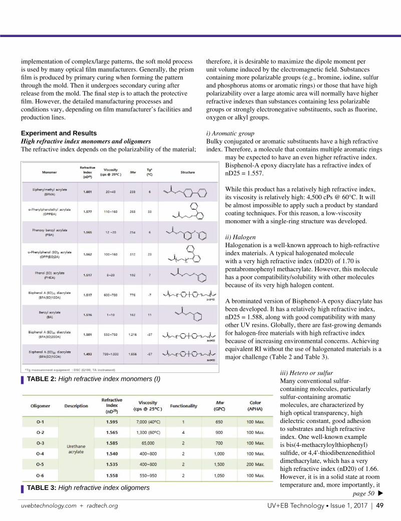
uvebtechnology.com + radtech.org UV+EB Technology • Issue 1, 2017 | 49
page 50 u
implementation of complex/large patterns, the soft mold process is used by many optical film manufacturers. Generally, the prism film is produced by primary curing when forming the pattern through the mold. Then it undergoes secondary curing after release from the mold. The final step is to attach the protective film. However, the detailed manufacturing processes and conditions vary, depending on film manufacturer’s facilities and production lines.
Experiment and ResultsHigh refractive index monomers and oligomersThe refractive index depends on the polarizability of the material;
therefore, it is desirable to maximize the dipole moment per unit volume induced by the electromagnetic field. Substances containing more polarizable groups (e.g., bromine, iodine, sulfur and phosphorus atoms or aromatic rings) or those that have high polarizability over a large atomic area will normally have higher refractive indexes than substances containing less polarizable groups or strongly electronegative substituents, such as fluorine, oxygen or alkyl groups.
i) Aromatic groupBulky conjugated or aromatic substituents have a high refractive index. Therefore, a molecule that contains multiple aromatic rings
may be expected to have an even higher refractive index. Bisphenol-A epoxy diacrylate has a refractive index of nD25 = 1.557.
While this product has a relatively high refractive index, its viscosity is relatively high: 4,500 cPs @ 60°C. It will be almost impossible to apply such a product by standard coating techniques. For this reason, a low-viscosity monomer with a single-ring structure was developed.
ii) HalogenHalogenation is a well-known approach to high-refractive index materials. A typical halogenated molecule with a very high refractive index (nD20) of 1.70 is pentabromophenyl methacrylate. However, this molecule has a poor compatibility/solubility with other molecules because of its very high halogen content.
A brominated version of Bisphenol-A epoxy diacrylate has been developed. It has a relatively high refractive index, nD25 = 1.588, along with good compatibility with many other UV resins. Globally, there are fast-growing demands for halogen-free materials with high refractive index because of increasing environmental concerns. Achieving equivalent RI without the use of halogenated materials is a major challenge (Table 2 and Table 3).
iii) Hetero or sulfurMany conventional sulfur-containing molecules, particularly sulfur-containing aromatic molecules, are characterized by high optical transparency, high dielectric constant, good adhesion to substrates and high refractive index. One well-known example is bis(4-methacryloylthiophenyl) sulfide, or 4,4'-thiodibenzenedithiol dimethacrylate, which has a very high refractive index (nD20) of 1.66. However, it is in a solid state at room temperature and, more importantly, it
TABLE 2: High refractive index monomers (I)
TABLE 3: High refractive index oligomers

50 | UV+EB Technology • Issue 1, 2017 uvebtechnology.com + radtech.org
t page 49
From Figure 7, we can find viscosity value when blending each monomer with O-3 at 30 percent, where O-3 corresponds to di-functional urethane acrylate. The highest quality of dilution power is observed with monomer BA. However, in case of BA, it tends to reduce the RI in the test formulation. In consideration, the most important point is to raise the refractive index.
Relating to this point, test results reveal that using BPMA or OPPEA will raise the RI formulation. Commercially, the preferred monomer is OPPEA, when taking dilution power and refractive index into account.
Recently, demand is increasing for slimmer displays and lower costs. To reach these demands, increased efforts are being made to reduce the number of optical films and to enhance brightness. Those efforts include a trial to remove the protective film that covers the outside of an optical film, using the film as it is. To avoid damage to the prism sheet’s lens detail, a product with enhanced hardness and scratch resistance must be developed. It is extremely difficult to increase the refractive index while maintaining scratch resistance.
In the course of this development work, products were obtained with enhanced elasticity by means of EO addition into fluorine-containing molecules with refractive index at a high level. The products, in which treatment of EO addition is given to fluorene structure, are M-4, M-5, M-6 and M-7 (Table 4).
One more important factor is hardness of optical film coating. We performed pencil hardness and pendulum hardness evaluation by coating test formulations on PET film typically used for prism sheet. EO addition type products are seen to be lower in hardness. However, this doesn’t mean the scratch property is lacking, as the EO functionality plays a role to keep the prism sheet’s details intact, courtesy of elasticity improvement. When comparing M-7 with M-4, the former contains more EO than the latter, resulting in an improvement in flexibility (Table 5).
FIGURE 7: Dilution power of monomers
TABLE 4: High refractive index monomers (II)
TABLE 5: Film properties of high RI oligomers and monomers – Hardness
has a very limited solubility/compatibility with other UV resins. Proprietary technologies have been developed to enable the synthesis of a series of heteroatom-containing aromatic urethane acrylate oligomers. These oligomers have a high refractive index, nD25=1.58 (liquid), and excellent optical transparency. Additionally, these oligomers are compatible with many commercial UV resins, thus making them easily formulated.
A high RI formulation for the prism sheet also requires low viscosity value for coating. Therefore, we recognize dilution power as being important for high RI formulation.
REFRACTIVE MATERIALS

uvebtechnology.com + radtech.org UV+EB Technology • Issue 1, 2017 | 51
It is found that most high refractive index materials tend to yellow due to the inclusion of a large number of aromatic rings (Figure 8). To minimize yellowing, trials were done (Figure 9). In the cases where halogen or sulfur structures are found, yellowing is significantly increased. To compound the problem, sulfur is accompanied with an odor issue, so these structures tend to not be favored.
The adhesion property is regarded as the most important one for coating application. All products show excellent or good adhesion on PET (Table 6). The adhesion properties of EO addition types also are excellent, even when the molecular weight is relatively high.
ConclusionDemand is quickly growing for new materials that have higher RI, higher performance and, especially, are halogen-free because of increasing environmental concerns. Achieving equivalent
RI without the use of halogenated materials is a big challenge. Based on a broad understanding of the refractive index, new technologies have now been developed to address this challenge, including heteroatom-containing materials. u
For more information, visit www.miramer.com.
TABLE 6: Film properties of high RI oligomers and monomers – Adhesion
FIGURE 8: Film properties of high RI monomers – Yellowing
FIGURE 9: Film properties of high RI oligomers and monomers – Yellowing
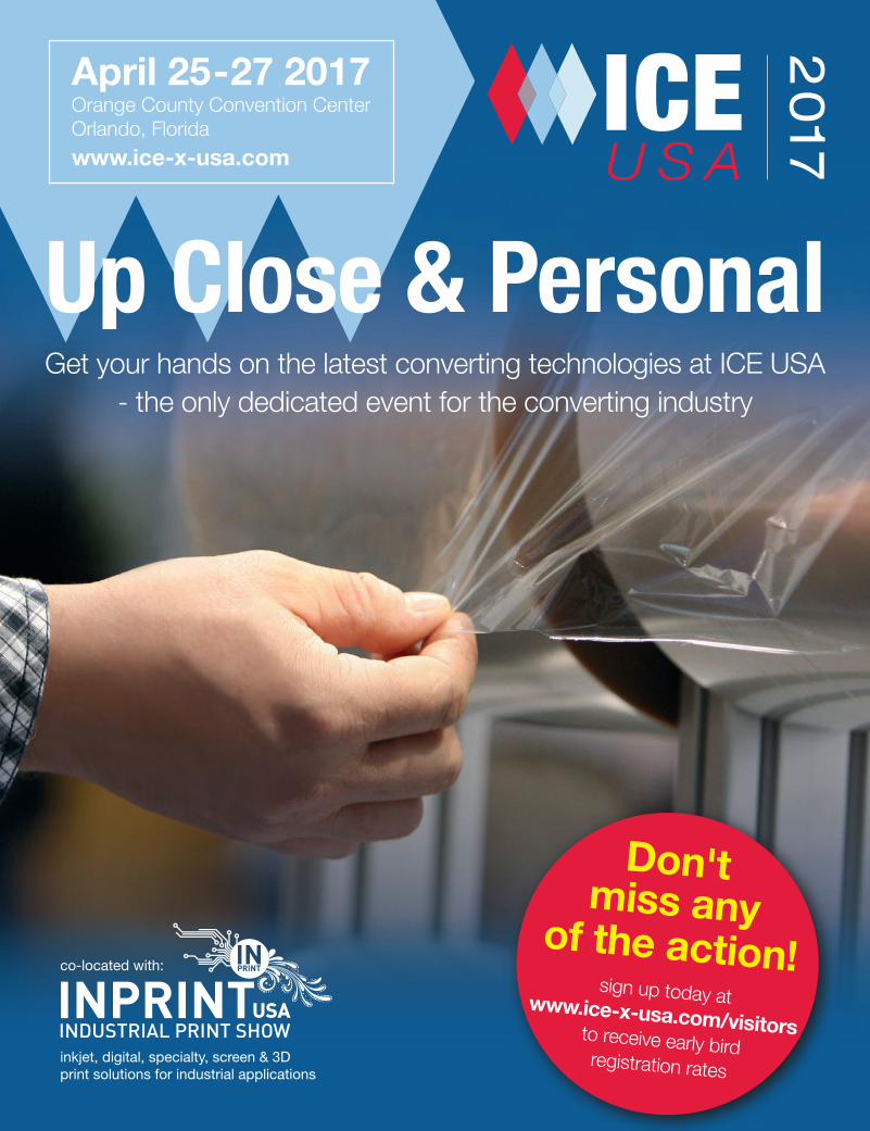
20
17April 25-27 2017Orange County Convention CenterOrlando, Florida
www.ice-x-usa.com
Get your hands on the latest converting technologies at ICE USA - the only dedicated event for the converting industry
Up Close & Personal
inkjet, digital, specialty, screen & 3Dprint solutions for industrial applications
co-located with:
sign up today at www.ice-x-usa.com/visitors to receive early birdregistration rates
Don'tmiss any
of the action!
uvebtechnology.com + radtech.org UV+EB Technology • Issue 1, 2017 | 53
Increasingly, 3D printers are being used in non-laboratory settings such as libraries, schools or workshops. While many
different technologies are used in 3D printing, UV-curable 3D printing is one of the easiest ways to print high-quality objects with superior resolution. The rapidly decreasing cost of the equipment has encouraged hobbyists, students and others who want UV-cure quality to dive into the technology – often without adequate preparation. It’s just a printer – right?
Not so, according to Mike Idacavage, vice president for business development at Colorado Photopolymer Solutions in Boulder and member of the UV+EB Technology editorial board.
“There are multiple concerns and a variety of areas that require people to be cautious,” he warned. “This is active chemistry.”
Finding the appropriate way to address that concern has been in the pipeline at RadTech for a couple of years. In January 2015, a group including Idacavage, RadTech Executive Director Gary Cohen, Senior Director Mickey Fortune and others began talking about how the organization could provide information to end users who are not scientists and might not be aware of the environmental or safety hazards.
The result of the group’s efforts is a set of recommendations entitled “UV 3D Printing Safe Handling Guide.” The guide is scheduled to be introduced at uv.ebWEST and the RadTech Annual Winter Meeting, February 27 through March 2 in San Francisco, California.
“We were discussing that this technology is going to consumers who might not be aware of how to safely handle the materials, and we felt it was our ethical responsibility to publish a fact sheet or poster telling users how to do that,” Idacavage said. “We wanted to do something before the technology became too common and someone was injured from not handling the equipment or materials correctly. That was our motivation.”
The group began developing the environmental health and safety (EHS) guide by considering what consumers would need to know to safely work with the technology. The next step was to ensure it could be read and understood by someone who did not have a background in chemistry or related science.
“I was shepherding it through development,” Idacavage continued, “and got feedback from other RadTech members along
EHS Guide Enhances Safety for Users of UV-Curable 3D PrintingBy Nancy Cates, contributing writer, UV+EB Technology
the way. Then, we took it to a more consumer-level audience. The reaction was ‘Why didn’t I have this when I first bought the machine?’ That told us were on the right track.
“They (end users) need to understand the chemical hazards and the ways they can be handled safely – that it’s not like handling the benign items in the kitchen. It’s important for them to know they need to use appropriate gloves and goggles, to keep food and drinks away from the area, how to clean up any spills and how they can handle and treat the materials with respect. They need to understand their responsibility to keep leftover fluids out of the water system and realize that the local municipality might classify partially cured or uncured resin as hazardous waste.”
In addition to soliciting feedback from end users, content developers also checked with a few vendors of the consumables and obtained positive responses. Several vendors indicated an interest in providing the EHS guide to their customers.
After a few more tweaks, the developers decided they needed to provide the information in a format that was graphically pleasing as well as simple to follow. They set up a competition with some graphic arts students at the University of Iowa.
“We had worked with that group before to develop some UV-curing posters with good results,” Idacavage said. “We gave them the basic information for the EHS sheets in December with a January 2017 deadline.”
Idacavage also mentioned a desire to obtain additional feedback on the text and design from RadTech members before the material is more broadly distributed in early March.
After the content and design are finalized, the EHS guide will be available for download on the RadTech website at www.radtech.org. The group plans to announce the availability of the information via media releases and through contacts with printer and resin vendors. u
Ultraviolet (UV) curable resins for 3D Printing/additive manufacturing cure instantly when exposed to UV light. As with all chemicals, UV curable resins must be
handled in a safe manner. This fact sheet is meant as a general guideline for the handling of UV curable resin materials (photopolymers) used in 3D printing
systems such as stereolithography (SLA), digital light processing (DLP) and UV inkjet.
CONSULT MANUFACTURER DOCUMENTATIONConsult Safety Data Sheets (SDSs) provided by suppliers of the UV curable resins as the primary safety and handling documents.3D printers have built-in safety features that are designed to prevent
operator exposure to uncured photopolymers and UV wavelengths – do not try to change or disable these features.
Avoid placing a 3D printer over carpeted areas or use a barrier to avoid the possibility of carpet damage. Do not expose UV curable resin to heat (at or above 110°C/ 230°F), flames, sparks, or any source of ignition.3D Printers and uncured, open resin vats should be stored and
operated in a well-ventilated area.If UV curable resin comes in a sealed cartridge: - Inspect the cartridge before loading it into the printer - Do not use a cartridge that is leaking or damaged. Dispose of it according to local regulations and contact the supplier.If the UV curable resin is in a pourable bottle, carefully pour the liquid
from the storage bottle into the printer tray, avoiding spills and drips.
Avoid direct contact with any UV curable resin, including any parts of the body or clothing.Wear appropriate chemical resistant gloves (nitrile or neoprene) – DO NOT use latex gloves.Use safety glasses/goggles with UV protection.Wear a dust mask when sanding or post-finishing parts.
Use absorbent rags to clean spills immediately.Clean any contacted or exposed surfaces to prevent contamination. Clean with window cleaner, or a denatured or isopropyl alcohol, followed by a thorough washing with soap and water.
Tools that may be contaminated with the material should be cleaned prior to reuse with window cleaner, or plenty of denatured or isopropyl alcohol, followed by a thorough washing with soap and water.Keep work area clean.
Wear gloves when handling parts directly from the printer. Ensure that all 3D Printed objects are fully post cured by exposure to a UV light source after forming, in accordance with the printer manufacturers’ recommendations. Wash the parts before post cure using a manufacturer’s recommended solvent, such as isopropyl or rubbing alcohol.Post cure using UV light as recommended by the manufacturer
should follow the wash before the printed object is handled without gloves.
Flush contaminated eyes or skin thoroughly with plenty of water for 15 minutes. Wash skin with soap and plenty of water or waterless cleaner if needed.If skin irritation or rash occurs, seek qualified medical attention.If ingested, do not induce vomiting, seek medical attention
immediately.
USE PERSONAL PROTECTIVE EQUIPMENT [PPE]
FOLLOW GOOD HOUSKEEPING PROCEDURESDURING SET UP
AFTER PRINTING
PRACTICE PERSONAL HYGIENECLEAN UP WORK AREAS
KNOW FIRST AID PROCEDURES
Do not eat, drink or smoke in work area. Remove jewelry (rings, watches, bracelets) prior to handling uncured UV curable materials.Avoid direct contact with any UV curable resins or contaminated
surfaces, including any parts of the body or clothing. Do not touch the resin without wearing protective gloves and do not get it on your skin.
Wash hands, face or any body parts that may contact UV curable resin with mild skin cleanser and soaps after handling – do not use solvents.
Remove and wash contaminated clothing or jewelry; do not reuse any contaminated personal items until properly cleaned with detergent; discard contaminated shoes and leather goods.
PREPARE FOR DISPOSALFully cured resin can be disposed of with household items.Cure unreacted UV curable resins by leaving them in sunlight for a few hours or expose them to a UV light.Partially cured or uncured resin waste may be classified as hazardous waste in some areas.Please check your state’s website for disposal of chemical waste. Do not pour into the sink or dispose into the water system.
Clean-up materials containing UV curable resins should be isolated in sealed, labeled containers and disposed of as hazardour waste. Do not pour these materials down the drain or into a water system.
STORE CORRECTLYKeep UV curable resins sealed tightly in their containers, out of direct sunlight, and within the temperature range suggested by the manufacturer.
A small headspace of air is needed to keep the reisn from gelling. Do not full resin containers to the top of the opening.Do not pour “used uncured resin” back into new resin bottles.Do not store uncured resin in refrigerators used for food and
beverage storage.
The information provided in Safe Handling of UV Curable 3D Printing Resins is believed to be current at the date of publication. The guidelines found in this Guide may not cover all applicable legal requirements. RadTech
is not responsible for the conditions of use of particular 3D printing systems. It is the user’s responsibility to determine the safe conditions of use of a particular 3D printing system. The guide is offered in good faith and
is believed to be reliable; however it provided neither warranties not representations for any of the products it mentions. RadTech disclaims any and all liability for the damages incurred directly or indirectly through the
use of this document. Nothing contained herein should be considered a recommendation to use any particular company’s product. Contact your checmical and equipment supplier for additional information.
RESIN SAFETY

54 | UV+EB Technology • Issue 1, 2017 uvebtechnology.com + radtech.org
Regulatory News
Doreen M. Monteleone, Ph.D., director of sustainability & EHS initiatives, RadTech International North America doreen@ radtech.org
Toxic Substances Control Act UpdateThere was much discussion at a recent RadTech EHS Committee meeting focusing on the revisions to the Toxic Substances Control Act (TSCA) as amended by the Lautenberg Chemical Safety for the 21st Century Act (LCSA). Although the rule is not yet final, responses from the US Environmental Protection Agency (US EPA) to new pre-manufacturing notices (PMNs) are being delayed or consent orders are being issued. RadTech held a webinar on this topic, archived at http://www.esf.edu/outreach/radcuring/webinar.htm#Marrapese2. More recently, US EPA has published a list of the first 10 chemicals it will evaluate for potential risks to human health and the environment under TSCA reform. Additional chemicals will be designated for evaluation, and all of the remaining Work Plan chemicals will be reviewed for their potential hazard and exposure. For each risk evaluation that US EPA completes, TSCA requires that the agency begin another. By the end of 2019, US EPA must have at least 20 chemical risk valuations ongoing at any given time. For more information, go to http://tinyurl.com/h5hggez.
On December 14, 2016, US EPA held a public meeting to update TSCA stakeholders and the public on changes to the TSCA. Presentations have been archived on US EPA’s website as follows: • Reviewing New Chemicals under the Toxic Substances Control Act: https://www.epa.gov/sites/
production/files/2016-12/documents/public_meeting_presentation_mjd_12_13_16_rev.pdf • Reviewing New Chemicals under the Toxic Substances Control Act: Science Issues: https://www.epa.
gov/sites/production/files/2016-12/documents/public_meeting_presentation.th_12-13-16.pdf• How to Make the Review Process More Efficient: https://www.epa.gov/sites/production/files/2016-12/
documents/public_meeting_presentation.gs_.12-13-2016.pdf
Listen to the recording and view slides presented at the public meeting at http://mp163422.cdn.mediaplatform.com/163422/wc/mp/4000/15208/30195/69304/Lobby/default.htm.
Hazardous Waste Generator Improvements Rule FinalizedUS EPA has finalized revisions to the Resource Conservation and Recovery Act (RCRA) hazardous waste generator regulatory program. Several controversial revisions include the following:• reorganizing the hazardous waste generator regulations to make them more user-friendly and thus
improve their usability by the regulated community;• providing a better understanding of how the RCRA hazardous waste generator regulatory program
works;• addressing gaps in the existing regulations to strengthen environmental protection to provide greater
flexibility for hazardous waste generators to manage their hazardous waste in a cost-effective and protective manner; and
• making technical corrections and conforming changes to address inadvertent errors and remove obsolete references to programs that no longer exist.
More information on RCRA can be found at https://www.epa.gov/hwgenerators/final-rule-hazardous-waste-generator-improvements.
OSHA Issues Proposed Changes to Lockout/Tagout Rule The Occupational Safety and Health Administration (OSHA) has proposed a controversial revision to the lockout/tagout rule under the Standards Improvement Project-Phase IV (SIP IV), a collection of 18 OSHA rule revisions changed to “remove or revise outdated, duplicative, unnecessary and inconsistent requirements” in OSHA’s standards. The current lockout/tagout standard applies to servicing and maintenance operations “in which the unexpected energization or startup of the machine or equipment, or release of stored energy could harm employees.” OSHA intends to revise the lockout/tagout rule by removing the word “unexpected,” such that the standard would apply to any energization, not just unexpected ones. More information about the changes to the lockout/tagout program can be found at https://www.osha.gov/pls/oshaweb/owadisp.show_document?p_table=FEDERAL_REGISTER&p_id=27533.
Sustainability Gains Traction in the Printing IndustryAlong with the major printing and ink associations, RadTech supports the Sustainable Green Printing
uvebtechnology.com + radtech.org UV+EB Technology • Issue 1, 2017 | 55
Regulatory News
Rita Loof, director of regional environmental affairs, RadTech International North America [email protected]
Partnership (SGP) as an SGP Resource Partner. As such, RadTech encourages its members to learn more and get involved with SGP in its effort to promote sustainable printing. Recent SGP activities include certification of the printer of the licensed apparel for Major League Baseball, the National Football League, the National Basketball Association, Harley-Davidson and other properties. SGP introduced a new multi-location certification program and an updated guidance document that reflects the changes in the 2016 SGP Criteria. Read about GFX International’s journey through the SGP process and how the certification has made the company more competitive at http://tinyurl.com/gkp959j. Learn more about SGP and how your company might get involved and help support the sustainable printing movement at www.sgppartnership.org.
News from the West CoastSCAQMD Staff Revisits BACT The South Coast Air Quality Management District (SCAQMD) recently proposed changes to its Best Available Control Technology (BACT) guidelines. BACT applies to any new or modified source. The guidelines had not been updated for more than 10 years. Due to RadTech’s opposition of the proposal brought forth in December 2016, the SCAQMD board unanimously supported resolution language proposed by RadTech, which read as follows:
“BE IT FURTHER RESOLVED that the Board directs AQMD staff to work with industry and other stakeholders on assessing Ultraviolet/Electron Beam (UV/EB) technology as an alternative to meet Best Available Control Technology. This analysis should include BACT determinations by other air districts. The staff analysis shall be presented to the board by June 2017. “
The language included a deadline of June 2017 to prevent another 10-year delay. RadTech (which holds a seat on the agency’s Local Government Small Business Committee) requested a status update. Staff gave a presentation in January and stated they are working with other air districts as well as reviewing permits. They also have visited district facilities that are currently using UV systems and reported that the operators had positive comments about the technology. Staff reported that RadTech’s application for membership on the BACT advisory committee is under consideration. Staff has requested cost information from RadTech to perform a cost-effective analysis. RadTech members that can provide cost data are urged to contact Rita Loof at [email protected]. Staff will continue with site visits and will report to the Stationary Source Committee by June of this year.
SCAQMD Seeks to Expand AuthorityThe South Coast Air Quality Management District is sponsoring legislation that would broaden its authority to shut down operations the agency believes present “an imminent and substantial endangerment to the public health or welfare, or the environment…” The proposal would give the air pollution control officer the power to issue an accusation against a company and issue an “order of abatement.” Staff is basing its approach on recent cases in the city of Paramount, where elevated levels of hexavalent chromium were found, purportedly due to aerospace operations.
Staff also presented a proposal that fines for violations be increased, arguing that the current fine structure does not present a sufficient deterrent to violators. SCAQMD board members questioned staff’s contentions and requested additional evidence that violators were performing a cost/benefit analysis based on the amount of the fines. Although staff has stated that a fine increase would only apply to “serious continuous violators,” no formal language has been presented for public review to support the argument. u
56 | UV+EB Technology • Issue 1, 2017 uvebtechnology.com + radtech.org
APRIL 10-11 Advanced Coatings 2017, Holiday Inn Houston-Webster – Clear Lake, Houston, Texas, advcoatings.org.
25-27 ICE USA, Orange County Convention Center, Orlando, Florida. For more information, visit ice-x-usa.com.
MAY 15-17 Eastern Coatings Show, Harrah’s Resort, Atlantic City, New Jersey. For more information, visit easterncoatingsshow.com.
15-18 UV DAYS 2017, IST METZ GmbH headquarters, Nürtingen, Germany, ist-uv.com/uvdays.
SEPTEMBER 17-20 Photopolymerization Fundamentals, St Julien Hotel & Spa, Boulder, Colorado, radtechintl.org/Photopolymer2017.
FEBRUARY 27-March 1 uv.eb WEST 2017 Materials + Manufacturing Summit, Embassy Suites San Francisco Airport Waterfront, San Francisco, California. For more information, visit uvebwest.com.
MARCH 1-2 RadTech Annual Winter Meeting, Embassy Suites San Francisco Airport Waterfront, San Francisco, California, radtech.org.
19-21 TAGA 2017 Annual Technical Conference, Houston Marriott West Loop by The Galleria, Houston, Texas, tagaatc.printing.org.
29-31 Print UV Conference, Encore by Wynn Las Vegas Resort, Las Vegas, Nevada, For more information, visit printuv.com.
Calendar
Advertisers’ Index
American Ultraviolet .................................................................americanultraviolet.com ........................................................................................ 9
A.W.T. World Trade Inc. ............................................................awt-gpi.com ..........................................................................................................45
BASF ..........................................................................................basf.us/dpsolutions ...................................................................Inside Front Cover
BCH Brühl ..................................................................................bch-bruehl.de .......................................................................................................41
EIT Instrument Markets ............................................................eit.com .................................................................................................................. 21
Eastern Coatings Show ............................................................easterncoatingsshow.com ................................................................................... 31
Excelitas Technologies .............................................................excelitas.com .........................................................................................Back Cover
GEW ...........................................................................................gewuv.com .............................................................................................................. 7
Heraeus Noblelight America LLC ...........................................heraeus-noblelight.com....................................................................................... 17
Honle UV America Inc. .............................................................honleuv.com ........................................................................................................... 5
ICE USA 2017 ............................................................................ ice-x-usa.com ........................................................................................................ 52
IGM Resins ................................................................................ igmresins.com/contact ..............................................................Inside Back Cover
Keyland Polymer .......................................................................keylandpolymer.com ............................................................................................ 23
Miwon Specialty Chemical Co., Ltd. .......................................miramer.com ......................................................................................................... 37
Phoseon Technology ................................................................phoseon.com ........................................................................................................ 33
Photopolymerization Fundamentals 2017 .............................. radtechintl.org/photopolymer2017 ....................................................................43
RAHN-Group ............................................................................. rahn-group.com...................................................................................................... 1
Sartomer Arkema Group .......................................................... sartomer.com ........................................................................................................ 19
Siltech Corporation .................................................................. siltech.com ............................................................................................................ 15
USHIO ........................................................................................ushio.com .............................................................................................................. 29

Gain a Competitive Edgein your UV Curing Process
OmniCure® UV LED Curing Solutions
www.excelitas.com [email protected] Argentia Road, Mississauga, Ontario, L5N 6H7 CANADA
Visit us at:
UV+EB West 2017February 28-March 1, 2017
San Francisco, CA
Improve product yields with low temperature curing
Enhance process control and reliability
Achieve consistent curing of adhesives, coatings and inks
Related Documents