R2045S/D 4-wire Serial Interface Real Time Clock Module NO.EA-113-100825 1 OUTLINE The R2045S/D is a real-time clock module, built in CMOS real-time clock IC and crystal oscillator, connected to the CPU by four signal lines, CE, SCLK, SI, and SO, and configured to perform serial transmission of time and calendar data to the CPU. The oscillation frequency is adjusted to high precision (0±5ppm: 15sec. per month at 25°C) The periodic interrupt circuit is configured to generate interrupt signals with six selectable interrupts ranging from 0.5 seconds to 1 month. The 2 alarm interrupt circuits generate interrupt signals at preset times. As the oscillation circuit is driven under constant voltage, fluctuation of the oscillator frequency due to supply voltage is small, and the time keeping current is small (TYP. 0.48μA at 3V). The oscillation halt sensing circuit can be used to judge the validity of internal data in such events as power-on; The supply voltage monitoring circuit is configured to record a drop in supply voltage below two selectable supply voltage monitoring threshold settings. The 32-kHz clock output function (N-channel Open drain output) is intended to output sub-clock pulses for the external microcomputer. The oscillation adjustment circuit is intended to adjust time by correcting deviations in the oscillation frequency of the crystal oscillator. FEATURES • Built in 32.768kHz crystal unit, The oscillation frequency is adjusted to high precision (0±5ppm: at 25°C) • Time keeping voltage 1.15V to 5.5V • Super low power consumption 0.48μA TYP (1.2μA MAX) at VDD=3V • Four signal lines (CE, SCLK, SI, and SO) required for connection to the CPU. • Time counters (counting hours, minutes, and seconds) and calendar counters (counting years, months, days, and weeks) (in BCD format) • Interrupt circuit configured to generate interrupt signals (with interrupts ranging from 0.5 seconds to 1 month) to the CPU and provided with an interrupt flag and an interrupt halt • 2 alarm interrupt circuits (Alarm_W for week, hour, and minute alarm settings and Alarm_D for hour and minute alarm settings) • 32768Hz clock output pin (N-channel open drain output) • With Power-on flag to prove that the power supply starts from 0V • With Oscillation halt sensing Flag to judge the validity of internal data • Supply voltage monitoring circuit with two supply voltage monitoring threshold settings • Automatic identification of leap years up to the year 2099 • Selectable 12-hour and 24-hour mode settings • Oscillation adjustment circuit for correcting temperature frequency deviation or offset deviation • CMOS process • Two types of package, SOP14(10.1x7.4x3.1) or SON22(6.1x5.0x1.3) *R2045D (SON22) is the non-promotion product. As of March in 2014.

Welcome message from author
This document is posted to help you gain knowledge. Please leave a comment to let me know what you think about it! Share it to your friends and learn new things together.
Transcript

R2045S/D
4-wire Serial Interface Real Time Clock Module NO.EA-113-100825
1
OUTLINE The R2045S/D is a real-time clock module, built in CMOS real-time clock IC and crystal oscillator, connected to the CPU by four signal lines, CE, SCLK, SI, and SO, and configured to perform serial transmission of time and calendar data to the CPU. The oscillation frequency is adjusted to high precision (0±5ppm: 15sec. per month at 25°C) The periodic interrupt circuit is configured to generate interrupt signals with six selectable interrupts ranging from 0.5 seconds to 1 month. The 2 alarm interrupt circuits generate interrupt signals at preset times. As the oscillation circuit is driven under constant voltage, fluctuation of the oscillator frequency due to supply voltage is small, and the time keeping current is small (TYP. 0.48μA at 3V). The oscillation halt sensing circuit can be used to judge the validity of internal data in such events as power-on; The supply voltage monitoring circuit is configured to record a drop in supply voltage below two selectable supply voltage monitoring threshold settings. The 32-kHz clock output function (N-channel Open drain output) is intended to output sub-clock pulses for the external microcomputer. The oscillation adjustment circuit is intended to adjust time by correcting deviations in the oscillation frequency of the crystal oscillator.
FEATURES • Built in 32.768kHz crystal unit, The oscillation frequency is adjusted to high precision (0±5ppm: at 25°C) • Time keeping voltage 1.15V to 5.5V • Super low power consumption 0.48μA TYP (1.2μA MAX) at VDD=3V • Four signal lines (CE, SCLK, SI, and SO) required for connection to the CPU. • Time counters (counting hours, minutes, and seconds) and calendar counters (counting years, months,
days, and weeks) (in BCD format) • Interrupt circuit configured to generate interrupt signals (with interrupts ranging from 0.5 seconds to 1
month) to the CPU and provided with an interrupt flag and an interrupt halt • 2 alarm interrupt circuits (Alarm_W for week, hour, and minute alarm settings and Alarm_D for hour and
minute alarm settings) • 32768Hz clock output pin (N-channel open drain output) • With Power-on flag to prove that the power supply starts from 0V • With Oscillation halt sensing Flag to judge the validity of internal data • Supply voltage monitoring circuit with two supply voltage monitoring threshold settings • Automatic identification of leap years up to the year 2099 • Selectable 12-hour and 24-hour mode settings • Oscillation adjustment circuit for correcting temperature frequency deviation or offset deviation • CMOS process • Two types of package, SOP14(10.1x7.4x3.1) or SON22(6.1x5.0x1.3)
*R2045D (SON22) is the non-promotion product. As of March in 2014.

R2045S/D
2
PIN CONFIGURATION
SCLK SO
VSS
VDD N.C.
1
2
3
4
5
6
7
9
TOP VIEW
R2045S (SOP14)
32KOUT
10
8
SI
11
12
13
14
N.C.
VPP
N.C.
N.C. CE
N.C.
INTR
SCLKSO
VSS
VDDCE 1
234567
9
TOP VIEW
R2045D (SON22)
32KOUT
10
8SI
11
1516
14
VPPN.C. N.C.
N.C.
N.C. N.C. N.C. N.C.
N.C.
N.C. N.C.
N.C.
1819
17
2122
20
INTR
BLOCK DIAGRAM
32kHz
OUTPUT CONTROL
OSC
COMPARATOR_DALARM_D REGISTER
(MIN,HOUR)
ADDRESS DECODER
ADDRESSREGISTER
VOLTAGEDETECT
DIV
TIME COUNTER (SEC,MIN,HOUR,WEEK,DAY,MONTH,YEAR)
SHIFT REGISTER
I/O CONTROL
32KOUT
INTERRUPT CONTROL
SCLK
DIVIDERCORREC
-TION
VDD
VSS
COMPARATOR_WALARM_W REGISTER
(MIN,HOUR, WEEK)
CE
OSC DETECT SI
TEST CIRCUIT
SO
VPP
INTR
*R2045D (SON22) is the non-promotion product. As of March in 2014.
R2045S/D
3
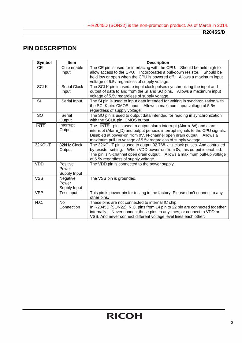
PIN DESCRIPTION
Symbol Item Description CE Chip enable
Input The CE pin is used for interfacing with the CPU. Should be held high to allow access to the CPU. Incorporates a pull-down resistor. Should be held low or open when the CPU is powered off. Allows a maximum input voltage of 5.5v regardless of supply voltage.
SCLK Serial Clock Input
The SCLK pin is used to input clock pulses synchronizing the input and output of data to and from the SI and SO pins. Allows a maximum input voltage of 5.5v regardless of supply voltage.
SI Serial Input The SI pin is used to input data intended for writing in synchronization with the SCLK pin. CMOS input. Allows a maximum input voltage of 5.5v regardless of supply voltage.
SO Serial Output
The SO pin is used to output data intended for reading in synchronization with the SCLK pin. CMOS output.
INTR Interrupt Output
The INTR pin is used to output alarm interrupt (Alarm_W) and alarm interrupt (Alarm_D) and output periodic interrupt signals to the CPU signals. Disabled at power-on from 0V. N-channel open drain output. Allows a maximum pull-up voltage of 5.5v regardless of supply voltage.
32KOUT 32kHz Clock Output
The 32KOUT pin is used to output 32.768-kHz clock pulses. And controlled by resister setting. When VDD power-on from 0v, this output is enabled. The pin is N-channel open drain output. Allows a maximum pull-up voltage of 5.5v regardless of supply voltage.
VDD Positive Power Supply Input
The VDD pin is connected to the power supply.
VSS Negative Power Supply Input
The VSS pin is grounded.
VPP Test input This pin is power pin for testing in the factory. Please don’t connect to any other pins.
N.C. No Connection
These pins are not connected to internal IC chip. In R2045D (SON22), N.C. pins from 14 pin to 22 pin are connected together internally. Never connect these pins to any lines, or connect to VDD or VSS. And never connect different voltage level lines each other.
*R2045D (SON22) is the non-promotion product. As of March in 2014.
R2045S/D
4
ABSOLUTE MAXIMUM RATINGS (VSS=0V)
Symbol Item Pin Name and Condition Description Unit VDD Supply Voltage VDD -0.3 to +6.5 V
Input Voltage 1 CE, SCLK, SI -0.3 to +6.5 VI Input Voltage 2 VPP -0.3 to VDD+0.3
V
Output Voltage 1 SO -0.3 to VDD+0.3 VO Output Voltage 2 INTR , 32KOUT -0.3 to +6.5
V
PD Power Dissipation Topt=25°C 300 mW Topt Operating
Temperature -40 to +85 °C
Tstg Storage Temperature -55 to +125 °C
RECOMMENDED OPERATING CONDITION (VSS=0V, Topt=-40 to +85°C)
Symbol Item Pin Name and Condition Min. Typ. Max.
Unit
VACCESS Supply Voltage VDD power supply voltage for interfacing with CPU
1.7 5.5 V
VCLK Time Keeping Voltage 1.15 5.5 V VPUP Pull-up Voltage INTR 5.5 V
FREQUENCY CHARACTERISTICS (VSS=0V)
Symbol Item Condition Min. Typ. Max. Unit Δf/f0 Frequency
Deviation Topt=25°C, VDD=3V -5 0 +5 ppm
Fv Frequency Voltage Characteristics
Topt=25°C, VDD=2.0V to 5.5V
-1 +1 ppm
Top Frequency Temperature Characteristics
Topt=-20°C to +70°C 25°C as standard
-120 +10 ppm
tsta Oscillation Start-up Time
Topt=25°C, VDD=2V +1 sec
fa Aging Topt=25°C, VDD=3V, First year
-5 +5 ppm
*R2045D (SON22) is the non-promotion product. As of March in 2014.
R2045S/D
5
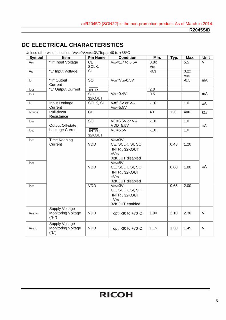
DC ELECTRICAL CHARACTERISTICS Unless otherwise specified: VSS=0V,VDD=3V,Topt=-40 to +85°C
Symbol Item Pin Name Condition Min. Typ. Max. UnitVIH “H” Input Voltage 0.8x
VDD 5.5
VIL “L” Input Voltage
CE, SCLK, SI
VDD=1.7 to 5.5V
-0.3 0.2x VDD
V
IOH “H” Output Current
SO VOH=VDD-0.5V -0.5 mA
IOL1 INTR 2.0 IOL2
“L” Output Current SO, 32KOUT
VOL=0.4V 0.5
mA
IIL Input Leakage Current
SCLK, SI VI=5.5V or VSS VDD=5.5V
-1.0 1.0 μA
RDNCE Pull-down Resistance
CE 40 120 400 kΩ
IOZ1 SO VO=5.5V or VSS VDD=5.5V
-1.0 1.0
IOZ2
Output Off-state Leakage Current
INTR , 32KOUT
VO=5.5V
-1.0 1.0
μA
IDD1 VDD
VDD=3V, CE, SCLK, SI, SO, INTR , 32KOUT
=VSS 32KOUT disabled
0.48
1.20
IDD2 VDD
VDD=5V, CE, SCLK, SI, SO, INTR , 32KOUT
=VSS
32KOUT disabled
0.60
1.80
IDD3
Time Keeping Current
VDD VDD=3V, CE, SCLK, SI, SO, INTR , 32KOUT
=VSS 32KOUT enabled
0.65 2.00
μA
VDETH
Supply Voltage Monitoring Voltage (“H”)
VDD
Topt=-30 to +70°C
1.90
2.10
2.30
V
VDETL
Supply Voltage Monitoring Voltage (“L”)
VDD
Topt=-30 to +70°C
1.15
1.30
1.45
V
*R2045D (SON22) is the non-promotion product. As of March in 2014.

R2045S/D
6
AC ELECTRICAL CHARACTERISTICS Unless otherwise specified: VSS=0V,Topt=-40 TO +85°C Input / Output condition: VIH=0.8xVDD,VIL=0.2xVDD,VOH=0.8xVDD,VOL=0.2xVDD,CL=50pF
VDD≥1.7V Symbol Item Condi- tions Min. Typ. Max.
Unit
tCES CE Set-up Time 400 ns tCEH CE Hold Time 400 ns tCR CE Recovery Time 62 μs fSCLK SCLK Clock Frequency 1.0 MHz tCKH SCLK Clock High Time 400 ns tCKL SCLK Clock Low Time 400 ns tCKS SCLK Set-up Time 200 ns tRD Data Output Delay Time 300 ns tRZ Data Output Floating Time 300 ns tCEZ Data Output Delay Time
After Falling of CE 300 ns
tDS Input Data Set-up Time 200 ns tDH Input Data Hold Time 200 ns
SCLK
tCES
SI
CE
tRD
tCKL
tCEZ
tDS tDH
tRD
tCEH
tCKH
tCKS tCR
tRZ
SO
*) For reading/writing timing, see “P.26 •Considerations in Reading and Writing Time Data under special condition”.
*R2045D (SON22) is the non-promotion product. As of March in 2014.

R2045S/D
7
PACKAGE DIMENSIONS
• R2045S (SOP14)
#14
#7 #1
#8
5.0±
0.2
10.1±0.2
7.4±
0.2
0.6 ±
0.25
0.15
0°-10°
0.35 1.27±0.1
0.1
3.2 ±
0.1
0.1
1.24typ.
3.1t
yp.
-0.0
5 -0.05 +0.1
+0.1
+0.1 -0.05
• R2045D (SON22)
A
6.1±0.2
#22 #14
#1 #11
4.7±0
.2
5.0±0
.2
0.2±0.1 0.5±0.1
0.10.125+0.1/-0.05
1.3±0.1
#1 #11
#22 #140.
3±0.1
0.43
0.43
0.
05
A
B
A’
B B
0.2
0.2
0.1
0.3
0.65
A’
0.3
0.20.55typ.
*R2045D (SON22) is the non-promotion product. As of March in 2014.

R2045S/D
8
GENERAL DESCRIPTION • Interface with CPU
The R2045S/D is connected to the CPU by four signal lines CE (Chip Enable), SCLK (Serial Clock), SI (Serial Input), and SO (Serial Output), through which it reads and writes data from and to the CPU. The CPU can be accessed when the CE pin is held high. Access clock pulses have a maximum frequency of 1 MHz allowing high-speed data transfer to the CPU.
• Clock and Calendar Function
The R2045S/D reads and writes time data from and to the CPU in units ranging from seconds to the last two digits of the calendar year. The calendar year will automatically be identified as a leap year when its last two digits are a multiple of 4. Consequently, leap years up to the year 2099 can automatically be identified as such.
• Alarm Function
The R2045S/D incorporates the alarm interrupt circuit configured to generate interrupt signals to the CPU at preset times. The alarm interrupt circuit allows two types of alarm settings specified by the Alarm_W registers and the Alarm_D registers. The Alarm_W registers allow week, hour, and minute alarm settings including combinations of multiple day-of-week settings such as "Monday, Wednesday, and Friday" and "Saturday and Sunday". The Alarm_D registers allow hour and minute alarm settings. The Alarm_W outputs from INTR pin, and the Alarm_D outputs also from INTR pin. Each alarm function can be checked from the CPU by using a polling function.
High-precision Oscillation Adjustment Function
To correct deviations in the oscillation frequency of the crystal oscillator, the oscillation adjustment circuit is configured to allow correction of a time count gain or loss (up to ±1.5 ppm at 25°C) from the CPU within a maximum range of approximately + 189 ppm in increments of approximately 3 ppm. Such oscillation frequency adjustment in each system has the following advantages:
* Corrects seasonal frequency deviations through seasonal oscillation adjustment. * Allows timekeeping with higher precision particularly with a temperature sensing function out of RTC,
through oscillation adjustment in tune with temperature fluctuations.
• Oscillation Halt Sensing Flag, Power-on Reset Flag, and Supply Voltage Monitoring Function
The R2045S/D incorporates an oscillation halt sensing circuit equipped with internal registers configured to record any past oscillation halt.
Power-on reset flag is set to “1” When R2045S/D is powered on from 0V. As such, the oscillation halt sensing flag and Power-on reset flag are useful for judging the validity of time
data. The R2045S/D also incorporates a supply voltage monitoring circuit equipped with internal registers
configured to record any drop in supply voltage below a certain threshold value. Supply voltage monitoring threshold settings can be selected between 2.1 and 1.3 volts through internal register settings. The oscillation halt sensing circuit is configured to confirm the established invalidation of time data in contrast to the supply voltage monitoring circuit intended to confirm the potential invalidation of time data. Further, the supply voltage monitoring circuit can be applied to battery supply voltage monitoring.
*R2045D (SON22) is the non-promotion product. As of March in 2014.
R2045S/D
9
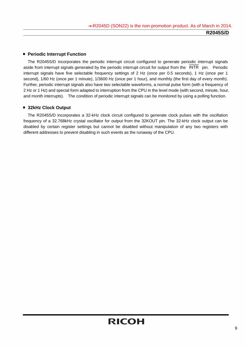
• Periodic Interrupt Function
The R2045S/D incorporates the periodic interrupt circuit configured to generate periodic interrupt signals aside from interrupt signals generated by the periodic interrupt circuit for output from the INTR pin. Periodic interrupt signals have five selectable frequency settings of 2 Hz (once per 0.5 seconds), 1 Hz (once per 1 second), 1/60 Hz (once per 1 minute), 1/3600 Hz (once per 1 hour), and monthly (the first day of every month). Further, periodic interrupt signals also have two selectable waveforms, a normal pulse form (with a frequency of 2 Hz or 1 Hz) and special form adapted to interruption from the CPU in the level mode (with second, minute, hour, and month interrupts). The condition of periodic interrupt signals can be monitored by using a polling function.
• 32kHz Clock Output
The R2045S/D incorporates a 32-kHz clock circuit configured to generate clock pulses with the oscillation frequency of a 32.768kHz crystal oscillator for output from the 32KOUT pin. The 32-kHz clock output can be disabled by certain register settings but cannot be disabled without manipulation of any two registers with different addresses to prevent disabling in such events as the runaway of the CPU.
*R2045D (SON22) is the non-promotion product. As of March in 2014.

R2045S/D
10
Address Mapping
Address Register Name
D a t a
A3A2A1A0 D7 D6 D5 D4 D3 D2 D1 D0 0 0 0 0 0 Second
Counter - *2)
S40 S20 S10 S8 S4 S2 S1
1 0 0 0 1 Minute Counter
- M40 M20 M10 M8 M4 M2 M1
2 0 0 1 0 Hour Counter - - H20 P/ A
H10 H8 H4 H2 H1
3 0 0 1 1 Day-of-week Counter
- - - - - W4 W2 W1
4 0 1 0 0 Day-of-month Counter
- - D20 D10 D8 D4 D2 D1
5 0 1 0 1 Month Counter and Century Bit
19 /20 - - MO10 MO8 MO4 MO2 MO1
6 0 1 1 0 Year Counter Y80 Y40 Y20 Y10 Y8 Y4 Y2 Y1 7 0 1 1 1 Oscillation
Adjustment Register *3)
(0) *4)
F6 F5 F4 F3 F2 F1 F0
8 1 0 0 0 Alarm_W (Minute Register)
- WM40 WM20 WM10 WM8 WM4 WM2 WM1
9 1 0 0 1 Alarm_W (Hour Register)
- - WH20 WP/ A
WH10 WH8 WH4 WH2 WH1
A 1 0 1 0 Alarm_W (Day-of-week Register)
- WW6 WW5 WW4 WW3 WW2 WW1 WW0
B 1 0 1 1 Alarm_D (Minute Register)
- DM40 DM20 DM10 DM8 DM4 DM2 DM1
C 1 1 0 0 Alarm_D (Hour Register)
- - DH20 DP/ A
DH10 DH8 DH4 DH2 DH1
D 1 1 0 1 - - - - - - - - E 1 1 1 0 Control
Register 1 *3) WALE DALE 12 /24 CLEN2
TEST CT2 CT1 CT0
F 1 1 1 1 Control Register 2 *3)
VDSL VDET XST PON *5)
CLEN1
CTFG WAFG DAFG
Notes: *1) All the data listed above accept both reading and writing. *2) The data marked with "-" is invalid for writing and reset to 0 for reading. *3) When the PON bit is set to 1 in Control Register 2, all the bits are reset to 0 in Oscillation Adjustment Register, Control Register 1 and Control Register 2 excluding the XST and PON bits. *4) The (0) bit should be set to 0. *5) XST is oscillation halt sensing bit. *6) PON is power-on reset flag.
*R2045D (SON22) is the non-promotion product. As of March in 2014.
R2045S/D
11
Register Settings • Control Register 1 (ADDRESS Eh)
D7 D6 D5 D4 D3 D2 D1 D0 WALE DALE 12 /24 CLEN2
TEST CT2 CT1 CT0 (For Writing)
WALE DALE 12 /24 CLEN2
TEST CT2 CT1 CT0 (For Reading)
0 0 0 0 0 0 0 0 Default Settings *) *) Default settings: Default value means read / written values when the PON bit is set to “1” due to VDD
power-on from 0 volts.
(1) WALE, DALE Alarm_W Enable Bit, Alarm_D Enable Bit WALE,DALE Description 0 Disabling the alarm interrupt circuit (under the control of the settings
of the Alarm_W registers and the Alarm_D registers). (Default)
1 Enabling the alarm interrupt circuit (under the control of the settings of the Alarm_W registers and the Alarm_D registers)
(2) 12 /24 12 /24-hour Mode Selection Bit
12 /24 Description 0 Selecting the 12-hour mode with a.m. and p.m. indications. (Default) 1 Selecting the 24-hour mode
Setting the 12 /24 bit to 0 and 1 specifies the 12-hour mode and the 24-hour mode, respectively.
24-hour mode 12-hour mode 24-hour mode 12-hour mode 00 12 (AM12) 12 32 (PM12) 01 01 (AM 1) 13 21 (PM 1) 02 02 (AM 2) 14 22 (PM 2) 03 03 (AM 3) 15 23 (PM 3) 04 04 (AM 4) 16 24 (PM 4) 05 05 (AM 5) 17 25 (PM 5) 06 06 (AM 6) 18 26 (PM 6) 07 07 (AM 7) 19 27 (PM 7) 08 08 (AM 8) 20 28 (PM 8) 09 09 (AM 9) 21 29 (PM 9) 10 10 (AM10) 22 30 (PM10) 11 11 (AM11) 23 31 (PM11)
Setting the 12 /24 bit should precede writing time data
(3) CLEN2 32-kHz Clock Output Bit2 CLEN2 Description
0 Enabling the 32-kHz clock output (Default) 1 Disabling the 32-kHz clock output
Setting the CLEN2 bits or the CLEN1 bit (D3 in the control register 2) to 0 specifies generating clock pulses with the oscillation frequency of the 32.768-kHz crystal oscillator for output from the 32KOUT pin.
Conversely, setting both the CLEN1 and the CLEN2 bit to 1 specifies disabling (“H”) such output.
*R2045D (SON22) is the non-promotion product. As of March in 2014.

R2045S/D
12
(4) TEST Test Bit TEST Description
0 Normal operation mode. (Default) 1 Test mode.
The TEST bit is used only for testing in the factory and should normally be set to 0.
(5) CT2,CT1, and CT0 Periodic Interrupt Selection Bits Description CT2 CT1 CT0
Wave form mode
Interrupt Cycle and Falling Timing
0 0 0 - OFF(H) (Default) 0 0 1 - Fixed at “L” 0 1 0 Pulse Mode
*1) 2Hz(Duty50%)
0 1 1 Pulse Mode *1)
1Hz(Duty50%)
1 0 0 Level Mode *2)
Once per 1 second (Synchronized with second counter increment)
1 0 1 Level Mode *2)
Once per 1 minute (at 00 seconds of every minute)
1 1 0 Level Mode *2)
Once per hour (at 00 minutes and 00 seconds of every hour)
1 1 1 Level Mode *2)
Once per month (at 00 hours, 00 minutes, and 00 seconds of first day of every month)
* 1) Pulse Mode: 2-Hz and 1-Hz clock pulses are output in synchronization with the increment of the second counter as illustrated in the timing chart below.
INTR Pin
Rewriting of the second counter
CTFG Bit
Approx. 92μs
(Increment of second counter) In the pulse mode, the increment of the second counter is delayed by approximately 92 μs from the falling edge of clock pulses. Consequently, time readings immediately after the falling edge of clock pulses may appear to lag behind the time counts of the real-time clocks by approximately 1 second. Rewriting the second counter will reset the other time counters of less than 1 second, driving the INTR pin low. * 2) Level Mode: Periodic interrupt signals are output with selectable interrupt cycle settings of 1 second, 1 minute, 1 hour, and 1 month. The increment of the second counter is synchronized with the falling edge of periodic interrupt signals. For example, periodic interrupt signals with an interrupt cycle setting of 1 second are output in synchronization with the increment of the second counter as illustrated in the timing chart below.
*R2045D (SON22) is the non-promotion product. As of March in 2014.

R2045S/D
13
CTFG Bit
INTR Pin
Setting CTFG bit to 0 Setting CTFG bit to 0
(Increment of
second counter) (Increment of
second counter) (Increment of
second counter)
*1), *2) When the oscillation adjustment circuit is used, the interrupt cycle will fluctuate once per 60sec. as follows: Pulse Mode: The “L” period of output pulses will increment or decrement by a maximum of ±3.784 ms. For example, 1-Hz clock pulses will have a duty cycle of 50 ±0.3784%. Level Mode: A periodic interrupt cycle of 1 second will increment or decrement by a maximum of ±3.784 ms.
• Control Register 2 (Address Fh) D7 D6 D5 D4 D3 D2 D1 D0
VDSL VDET XST PON CLEN1
CTFG WAFG
DAFG (For Writing)
VDSL VDET XST PON CLEN1
CTFG WAFG
DAFG (For Reading)
0 0 Indefinite 1 0 0 0 0 Default Settings *) *) Default settings: Default value means read / written values when the PON bit is set to “1” due to VDD power-on from 0 volts.
(1) VDSL VDD Supply Voltage Monitoring Threshold Selection Bit VDSL Description
0 Selecting the VDD supply voltage monitoring threshold setting of 2.1v. (Default) 1 Selecting the VDD supply voltage monitoring threshold setting of 1.3v.
The VDSL bit is intended to select the VDD supply voltage monitoring threshold settings.
(2) VDET Supply Voltage Monitoring Result Indication Bit VDET Description
0 Indicating supply voltage above the supply voltage monitoring threshold settings.
(Default)
1 Indicating supply voltage below the supply voltage monitoring threshold settings.
Once the VDET bit is set to 1, the supply voltage monitoring circuit will be disabled while the VDET bit will hold the setting of 1. The VDET bit accepts only the writing of 0, which restarts the supply voltage monitoring circuit. Conversely, setting the VDET bit to 1 causes no event.
(3) XST Oscillation Halt Sensing Monitor Bit XST Description
0 Sensing a halt of oscillation 1 Sensing a normal condition of oscillation
*R2045D (SON22) is the non-promotion product. As of March in 2014.
R2045S/D
14
The XST accepts the reading and writing of 0 and 1. The XST bit will be set to 0 when the oscillation halt sensing. The XST bit will hold 0 even after the restart of oscillation.
(4) PON Power-on-reset Flag Bit
PON Description 0 Normal condition 1 Detecting VDD power-on -reset (Default)
The PON bit is for sensing power-on reset condition. * The PON bit will be set to 1 when VDD power-on from 0 volts. The PON bit will hold the setting of 1 even after power-on. * When the PON bit is set to 1, all bits will be reset to 0, in the Oscillation Adjustment Register, Control Register 1, and Control Register 2, except XST and PON. As a result, INTR pin stops outputting, and 32KOUT starts outputting. * The PON bit accepts only the writing of 0. Conversely, setting the PON bit to 1 causes no event.
(5) CLEN1 32-kHz Clock Output Bit 1
CLEN1 Description
0 Enabling the 32-kHz clock output (Default)
1 Disabling the 32-kHz clock output
Setting the CLEN1 bit or the CLEN2 bit (D4 in the control register 1) to 0 specifies generating clock pulses with the oscillation frequency of the 32.768-kHz crystal oscillator for output from the 32KOUT pin. Conversely, setting both the CLEN1 and the CLEN2 bit to 1 specifies disabling (“H”) such output.
(6) CTFG Periodic Interrupt Flag Bit CTFG Description
0 Periodic interrupt output = “H” (Default) 1 Periodic interrupt output = “L”
The CTFG bit is set to 1 when the periodic interrupt signals are output from the INTR pin (“L”). The CTFG bit accepts only the writing of 0 in the level mode, which disables (“H”) the INTR pin until it is enabled (“L”) again in the next interrupt cycle. Conversely, setting the CTFG bit to 1 causes no event.
(7) WAFG,DAFG Alarm_W Flag Bit and Alarm_D Flag Bit WAFG,DAFG Description 0 Indicating a mismatch between current time and preset alarm time (Default) 1 Indicating a match between current time and preset alarm time
The WAFG and DAFG bits are valid only when the WALE and DALE have the setting of 1, which is caused approximately 61μs after any match between current time and preset alarm time specified by the Alarm_W registers and the Alarm_D registers. The WAFG (DAFG) bit accepts only the writing of 0. INTR pin outputs off (“H”) when this bit is set to 0. And INTR pin outputs “L” again at the next preset alarm time. Conversely, setting the WAFG and DAFG bits to 1 causes no event. The WAFG and DAFG bits will have the reading of 0 when the alarm interrupt circuit is disabled with the WALE and DALE bits set to 0. The settings of the WAFG (DAFG) bit is synchronized with the output of the INTR pin as shown in the timing chart below.
*R2045D (SON22) is the non-promotion product. As of March in 2014.
R2045S/D
15
INTR Pin
Writing of 0 to WAFG(DAFG) bit
WAFG(DAFG) Bit
(Match between
current time and
preset alarm time)
Approx. 61μs Approx. 61μs
Writing of 0 to WAFG(DAFG) bit
(Match between
current time and
preset alarm time)
(Match between
current time and
preset alarm time)
• Time Counter (Address 0-2h) Second Counter (Address 0h)
D7 D6 D5 D4 D3 D2 D1 D0 - S40 S20 S10 S8 S4 S2 S1 (For Writing) 0 S40 S20 S10 S8 S4 S2 S1 (For Reading) 0 Indefi
nite Indefinite
Indefinite
Indefinite
Indefinite
Indefinite
Indefinite
Default Settings *)
Minute Counter (Address 1h)
D7 D6 D5 D4 D3 D2 D1 D0 - M40 M20 M10 M8 M4 M2 M1 (For Writing) 0 M40 M20 M10 M8 M4 M2 M1 (For Reading) 0 Indefi
nite Indefinite
Indefinite
Indefinite
Indefinite
Indefinite
Indefinite
Default Settings *)
Hour Counter (Address 2h)
D7 D6 D5 D4 D3 D2 D1 D0 - - P/ A
or H20
H10 H8 H4 H2 H1 (For Writing)
0 0 P/ A or H20
H10 H8 H4 H2 H1 (For Reading)
0 0 Indefinite
Indefinite
Indefinite
Indefinite
Indefinite
Indefinite
Default Settings *)
*) Default settings: Default value means read / written values when the PON bit is set to “1” due to VDD power-on from 0 volts. * Time digit display (BCD format) as follows: The second digits range from 00 to 59 and are carried to the minute digit in transition from 59 to 00. The minute digits range from 00 to 59 and are carried to the hour digits in transition from 59 to 00. The hour digits range as shown in "P11 •Control Register 1 (ADDRESS Eh) (2) 12 /24: 12 -24-hour
Mode Selection Bit" and are carried to the day-of-month and day-of-week digits in transition from PM11 to AM12 or from 23 to 00.
*R2045D (SON22) is the non-promotion product. As of March in 2014.
R2045S/D
16
* Any writing to the second counter resets divider units of less than 1 second. * Any carry from lower digits with the writing of non-existent time may cause the time counters to
malfunction. Therefore, such incorrect writing should be replaced with the writing of existent time data.
• Day-of-week Counter (Address 3h)
D7 D6 D5 D4 D3 D2 D1 D0 - - - - - W4 W2 W1 (For Writing) 0 0 0 0 0 W4 W2 W1 (For Reading) 0 0 0 0 0 Indefi
nite Indefinite
Indefinite
Default Settings *)
*) Default settings: Default value means read / written values when the PON bit is set to “1” due to VDD power-on from 0 volts. * The day-of-week counter is incremented by 1 when the day-of-week digits are carried to the day-of-month
digits. * Day-of-week display (incremented in septimal notation):
(W4, W2, W1) = (0, 0, 0) → (0, 0, 1)→…→(1, 1, 0) → (0, 0, 0) * Correspondences between days of the week and the day-of-week digits are user-definable (e.g. Sunday = 0, 0, 0) * The writing of (1, 1, 1) to (W4, W2, W1) is prohibited except when days of the week are unused.
• Calendar Counter (Address 4-6h)
Day-of-month Counter (Address 4h) D7 D6 D5 D4 D3 D2 D1 D0 - - D20 D10 D8 D4 D2 D1 (For Writing) 0 0 D20 D10 D8 D4 D2 D1 (For Reading) 0 0 Indefi
nite Indefinite
Indefinite
Indefinite
Indefinite
Indefinite
Default Settings *)
Month Counter + Century Bit (Address 5h)
D7 D6 D5 D4 D3 D2 D1 D0 19 /20 - - MO10 MO8 MO4 MO2 MO1 (For Writing) 19 /20 0 0 MO10 MO8 MO4 MO2 MO1 (For Reading) Indefinite
0 0 Indefinite
Indefinite
Indefinite
Indefinite
Indefinite
Default Settings *)
Year Counter (Address 6h)
D7 D6 D5 D4 D3 D2 D1 D0 Y80 Y40 Y20 Y10 Y8 Y4 Y2 Y1 (For Writing) Y80 Y40 Y20 Y10 Y8 Y4 Y2 Y1 (For Reading)
Indefinite
Indefinite
Indefinite
Indefinite
Indefinite
Indefinite
Indefinite
Indefinite
Default Settings *)
*) Default settings: Default value means read / written values when the PON bit is set to “1” due to VDD power-on from 0 volts. * The calendar counters are configured to display the calendar digits in BCD format by using the automatic
*R2045D (SON22) is the non-promotion product. As of March in 2014.
R2045S/D
17
calendar function as follows: The day-of-month digits (D20 to D1) range from 1 to 31 for January, March, May, July, August, October, and December; from 1 to 30 for April, June, September, and November; from 1 to 29 for February in leap years; from 1 to 28 for February in ordinary years. The day-of-month digits are carried to the month digits in reversion from the last day of the month to 1. The month digits (MO10 to MO1) range from 1 to 12 and are carried to the year digits in reversion from 12 to 1. The year digits (Y80 to Y1) range from 00 to 99 (00, 04, 08, …, 92, and 96 in leap years) and are carried to the 19 /20 digits in reversion from 99 to 00. The 19 /20 digits cycle between 0 and 1 in reversion from 99 to 00 in the year digits. * Any carry from lower digits with the writing of non-existent calendar data may cause the calendar counters to malfunction. Therefore, such incorrect writing should be replaced with the writing of existent calendar data.
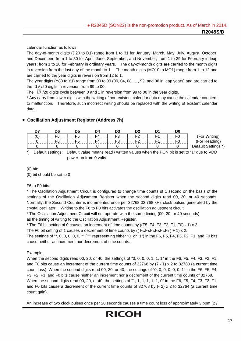
• Oscillation Adjustment Register (Address 7h)
D7 D6 D5 D4 D3 D2 D1 D0 (0) F6 F5 F4 F3 F2 F1 F0 (For Writing) 0 F6 F5 F4 F3 F2 F1 F0 (For Reading) 0 0 0 0 0 0 0 0 Default Settings *)
*) Default settings: Default value means read / written values when the PON bit is set to “1” due to VDD power-on from 0 volts. (0) bit: (0) bit should be set to 0 F6 to F0 bits: * The Oscillation Adjustment Circuit is configured to change time counts of 1 second on the basis of the settings of the Oscillation Adjustment Register when the second digits read 00, 20, or 40 seconds. Normally, the Second Counter is incremented once per 32768 32.768-kHz clock pulses generated by the crystal oscillator. Writing to the F6 to F0 bits activates the oscillation adjustment circuit. * The Oscillation Adjustment Circuit will not operate with the same timing (00, 20, or 40 seconds) as the timing of writing to the Oscillation Adjustment Register. * The F6 bit setting of 0 causes an increment of time counts by ((F5, F4, F3, F2, F1, F0) - 1) x 2. The F6 bit setting of 1 causes a decrement of time counts by (( F5,F4,F3,F2,F1,F0 ) + 1) x 2. The settings of "*, 0, 0, 0, 0, 0, *" ("*" representing either "0" or "1") in the F6, F5, F4, F3, F2, F1, and F0 bits cause neither an increment nor decrement of time counts. Example: When the second digits read 00, 20, or 40, the settings of "0, 0, 0, 0, 1, 1, 1" in the F6, F5, F4, F3, F2, F1, and F0 bits cause an increment of the current time counts of 32768 by (7 - 1) x 2 to 32780 (a current time count loss). When the second digits read 00, 20, or 40, the settings of "0, 0, 0, 0, 0, 0, 1" in the F6, F5, F4, F3, F2, F1, and F0 bits cause neither an increment nor a decrement of the current time counts of 32768. When the second digits read 00, 20, or 40, the settings of "1, 1, 1, 1, 1, 1, 0" in the F6, F5, F4, F3, F2, F1, and F0 bits cause a decrement of the current time counts of 32768 by (- 2) x 2 to 32764 (a current time count gain). An increase of two clock pulses once per 20 seconds causes a time count loss of approximately 3 ppm (2 /
*R2045D (SON22) is the non-promotion product. As of March in 2014.

R2045S/D
18
(32768 x 20 = 3.051 ppm). Conversely, a decrease of two clock pulses once per 20 seconds causes a time count gain of 3 ppm. Consequently, deviations in time counts can be corrected with a precision of ±1.5 ppm. Note that the oscillation adjustment circuit is configured to correct deviations in time counts and not the oscillation frequency of the 32.768-kHz clock pulses. For further details, see "P28 Configuration of Oscillation Circuit and Correction of Time Count Deviations •Oscillation Adjustment Circuit".
• Alarm_W Registers (Address 8-Ah)
Alarm_W Minute Register (Address 8h) D7 D6 D5 D4 D3 D2 D1 D0 - WM40 WM20 WM10 WM8 WM4 WM2 WM1 (For Writing) 0 WM40 WM20 WM10 WM8 WM4 WM2 WM1 (For Reading) 0 Indefi
nite Indefinite
Indefinite
Indefinite
Indefinite
Indefinite
Indefinite
Default Settings *)
Alarm_W Hour Register (Address 9h)
D7 D6 D5 D4 D3 D2 D1 D0 - - WH20
WP/ A WH10 WH8 WH4 WH2 WH1 (For Writing)
0 0 WH20 WP/ A
WH10 WH8 WH4 WH2 WH1 (For Reading)
0 0 Indefinite
Indefinite
Indefinite
Indefinite
Indefinite
Indefinite
Default Settings *)
Alarm_W Day-of-week Register (Address Ah)
D7 D6 D5 D4 D3 D2 D1 D0 - WW6 WW5 WW4 WW3 WW2 WW1 WW0 (For Writing) 0 WW6 WW5 WW4 WW3 WW2 WW1 WW0 (For Reading) 0 Indefi
nite Indefinite
Indefinite
Indefinite
Indefinite
Indefinite
Indefinite
Default Settings *)
*) Default settings: Default value means read / written values when the PON bit is set to “1” due to VDD power-on from 0 volts. * The D5 bit of the Alarm_W Hour Register represents WP/ A when the 12-hour mode is selected (0 for a.m. and 1 for p.m.) and WH20 when the 24-hour mode is selected (tens in the hour digits). * The Alarm_W Registers should not have any non-existent alarm time settings. (Note that any mismatch between current time and preset alarm time specified by the Alarm_W registers may disable the alarm interrupt circuit.) * When the 12-hour mode is selected, the hour digits read 12 and 32 for 0 a.m. and 0 p.m., respectively. (See "P11 •Control Register 1 (ADDRESS Eh) (2) 12 /24: 12-/24-hour Mode Selection Bit") * WW0 to WW6 correspond to W4, W2, and W1 of the day-of-week counter with settings ranging from (0, 0, 0) to (1, 1, 0). * WW0 to WW6 with respective settings of 0 disable the outputs of the Alarm_W Registers.
*R2045D (SON22) is the non-promotion product. As of March in 2014.
R2045S/D
19
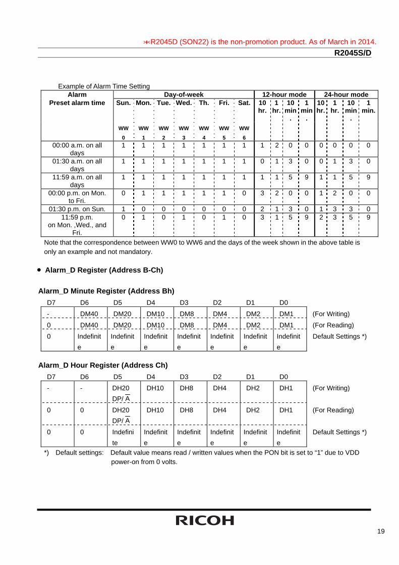
Example of Alarm Time Setting
Alarm Day-of-week 12-hour mode 24-hour mode Preset alarm time Sun. Mon. Tue. Wed. Th. Fri. Sat. 10
hr.1
hr.10
min.
1 min
.
10 hr.
1hr.
10min
.
1 min.
WW
0
WW
1
WW
2
WW
3
WW
4
WW
5
WW
6
00:00 a.m. on all days
1 1 1 1 1 1 1 1 2 0 0 0 0 0 0
01:30 a.m. on all days
1 1 1 1 1 1 1 0 1 3 0 0 1 3 0
11:59 a.m. on all days
1 1 1 1 1 1 1 1 1 5 9 1 1 5 9
00:00 p.m. on Mon. to Fri.
0 1 1 1 1 1 0 3 2 0 0 1 2 0 0
01:30 p.m. on Sun. 1 0 0 0 0 0 0 2 1 3 0 1 3 3 0 11:59 p.m.
on Mon. ,Wed., and Fri.
0 1 0 1 0 1 0 3 1 5 9 2 3 5 9
Note that the correspondence between WW0 to WW6 and the days of the week shown in the above table is only an example and not mandatory.
• Alarm_D Register (Address B-Ch)
Alarm_D Minute Register (Address Bh) D7 D6 D5 D4 D3 D2 D1 D0
- DM40 DM20 DM10 DM8 DM4 DM2 DM1 (For Writing)
0 DM40 DM20 DM10 DM8 DM4 DM2 DM1 (For Reading)
0 Indefinite
Indefinite
Indefinite
Indefinite
Indefinite
Indefinite
Indefinite
Default Settings *)
Alarm_D Hour Register (Address Ch)
D7 D6 D5 D4 D3 D2 D1 D0
- - DH20 DP/ A
DH10 DH8 DH4 DH2 DH1 (For Writing)
0 0 DH20 DP/ A
DH10 DH8 DH4 DH2 DH1 (For Reading)
0 0 Indefinite
Indefinite
Indefinite
Indefinite
Indefinite
Indefinite
Default Settings *)
*) Default settings: Default value means read / written values when the PON bit is set to “1” due to VDD power-on from 0 volts.
*R2045D (SON22) is the non-promotion product. As of March in 2014.

R2045S/D
20
* The D5 bit represents DP/ A when the 12-hour mode is selected (0 for a.m. and 1 for p.m.) and DH20 when the 24-hour mode is selected (tens in the hour digits). * The Alarm_D registers should not have any non-existent alarm time settings. (Note that any mismatch between current time and preset alarm time specified by the Alarm_D registers may disable the alarm interrupt circuit.) * When the 12-hour mode is selected, the hour digits read 12 and 32 for 0a.m. and 0p.m., respectively. (See "P11 •Control Register 1 (ADDRESS Eh) (2) 12 /24: 12/24-hour Mode Selection Bit")
*R2045D (SON22) is the non-promotion product. As of March in 2014.
R2045S/D
21
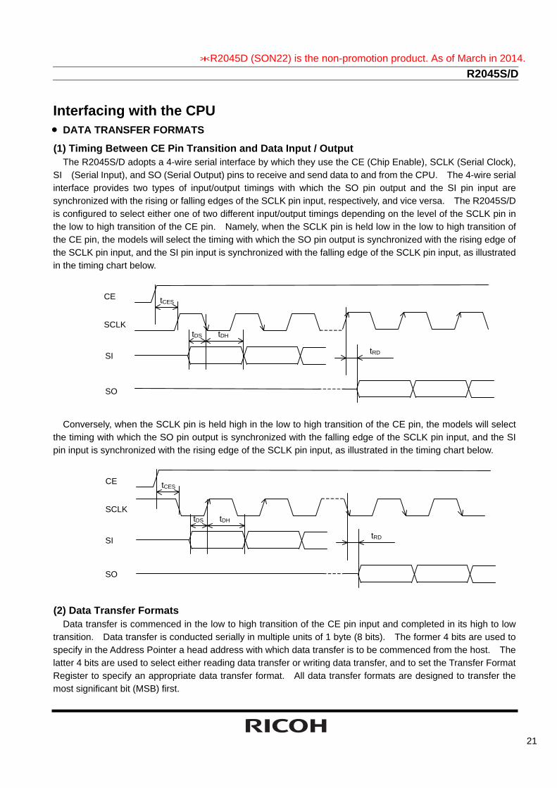
Interfacing with the CPU • DATA TRANSFER FORMATS
(1) Timing Between CE Pin Transition and Data Input / Output The R2045S/D adopts a 4-wire serial interface by which they use the CE (Chip Enable), SCLK (Serial Clock),
SI (Serial Input), and SO (Serial Output) pins to receive and send data to and from the CPU. The 4-wire serial interface provides two types of input/output timings with which the SO pin output and the SI pin input are synchronized with the rising or falling edges of the SCLK pin input, respectively, and vice versa. The R2045S/D is configured to select either one of two different input/output timings depending on the level of the SCLK pin in the low to high transition of the CE pin. Namely, when the SCLK pin is held low in the low to high transition of the CE pin, the models will select the timing with which the SO pin output is synchronized with the rising edge of the SCLK pin input, and the SI pin input is synchronized with the falling edge of the SCLK pin input, as illustrated in the timing chart below.
SCLK
SO
tDS
SI
CE tCES
tDH
tRD
Conversely, when the SCLK pin is held high in the low to high transition of the CE pin, the models will select
the timing with which the SO pin output is synchronized with the falling edge of the SCLK pin input, and the SI pin input is synchronized with the rising edge of the SCLK pin input, as illustrated in the timing chart below.
SCLK
SO
tDS
SI
CE tCES
tDH
tRD
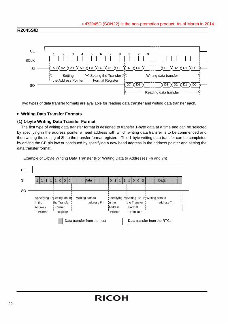
(2) Data Transfer Formats Data transfer is commenced in the low to high transition of the CE pin input and completed in its high to low
transition. Data transfer is conducted serially in multiple units of 1 byte (8 bits). The former 4 bits are used to specify in the Address Pointer a head address with which data transfer is to be commenced from the host. The latter 4 bits are used to select either reading data transfer or writing data transfer, and to set the Transfer Format Register to specify an appropriate data transfer format. All data transfer formats are designed to transfer the most significant bit (MSB) first.
*R2045D (SON22) is the non-promotion product. As of March in 2014.
R2045S/D
22
A2
CE
SCLK
SO
6
A1 A0 C3 C2 C1 C0
D7 D6 D3 D2 D1 D0
A3
75 8 2 312 3 1 4
D7 D6 D3 D2 D1 D0
Reading data transfer
Setting the Address Pointer
Writing data transfer Setting the TransferFormat Register
SI
Two types of data transfer formats are available for reading data transfer and writing data transfer each.
• Writing Data Transfer Formats
(1) 1-byte Writing Data Transfer Format The first type of writing data transfer format is designed to transfer 1-byte data at a time and can be selected
by specifying in the address pointer a head address with which writing data transfer is to be commenced and then writing the setting of 8h to the transfer format register. This 1-byte writing data transfer can be completed by driving the CE pin low or continued by specifying a new head address in the address pointer and setting the data transfer format.
1 1 Data Data
Example of 1-byte Writing Data Transfer (For Writing Data to Addresses Fh and 7h)
Data transfer from the host
CE
Data transfer from the RTCs
SO
Specifying 7hin theAddress Pointer
01 0 01 1
Setting 8h inthe Transfer Format Register
Writing data to address Fh
Writing data to address 7h
0 11 0 0 01 1
Specifying Fhin theAddress Pointer
Setting 8h inthe Transfer Format Register
SI
*R2045D (SON22) is the non-promotion product. As of March in 2014.
R2045S/D
23
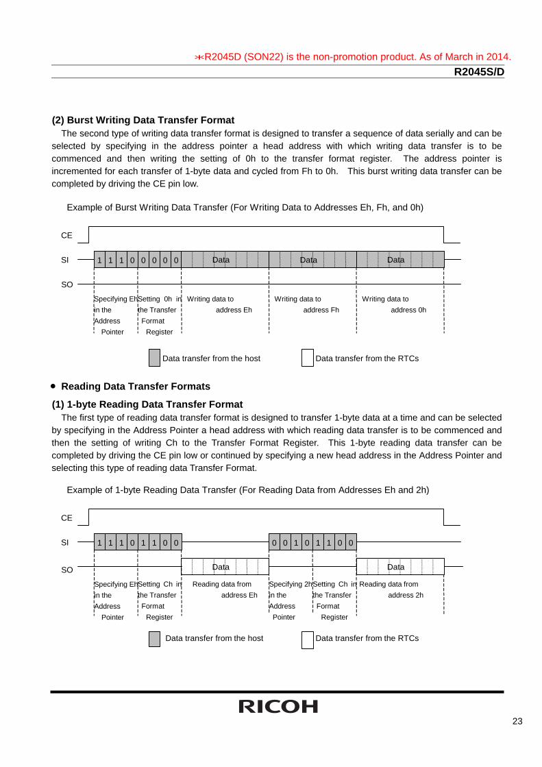
(2) Burst Writing Data Transfer Format
The second type of writing data transfer format is designed to transfer a sequence of data serially and can be selected by specifying in the address pointer a head address with which writing data transfer is to be commenced and then writing the setting of 0h to the transfer format register. The address pointer is incremented for each transfer of 1-byte data and cycled from Fh to 0h. This burst writing data transfer can be completed by driving the CE pin low.
1 0 Data Data
Example of Burst Writing Data Transfer (For Writing Data to Addresses Eh, Fh, and 0h)
CE
SO
00 0 01 1SI Data
Data transfer from the host Data transfer from the RTCs
Writing data to address Eh
Specifying Ehin theAddress Pointer
Setting 0h inthe Transfer Format Register
Writing data to address Fh
Writing data to address 0h
• Reading Data Transfer Formats
(1) 1-byte Reading Data Transfer Format The first type of reading data transfer format is designed to transfer 1-byte data at a time and can be selected
by specifying in the Address Pointer a head address with which reading data transfer is to be commenced and then the setting of writing Ch to the Transfer Format Register. This 1-byte reading data transfer can be completed by driving the CE pin low or continued by specifying a new head address in the Address Pointer and selecting this type of reading data Transfer Format.
1 0
Data Data
Example of 1-byte Reading Data Transfer (For Reading Data from Addresses Eh and 2h)
CE
SO
11 0 01 1 0 10 1 0 00 1SI
Data transfer from the host Data transfer from the RTCs
Specifying 2hin theAddress Pointer
Setting Ch inthe Transfer Format Register
Reading data from address Eh
Reading data from address 2h
Specifying Ehin theAddress Pointer
Setting Ch inthe Transfer Format Register
*R2045D (SON22) is the non-promotion product. As of March in 2014.

R2045S/D
24
(2) Burst Reading Data Transfer Format
The second type of reading data transfer format is designed to transfer a sequence of data serially and can be selected by specifying in the address pointer a head address with which reading data transfer is to be commenced and then writing the setting of 4h to the transfer format register. The address pointer is incremented for each transfer of 1-byte data and cycled from Fh to 0h. This burst reading data transfer can be completed by driving the CE pin low.
1 1
DATA DATA
Example of Burst Reading Data Transfer (For Reading Data from Addresses Fh, 0h, and 1h)
CE
SO
10 0 01 1
DATA
SI
Data transfer from the host Data transfer from the RTCs
Reading data from address Fh
Specifying Fhin theAddress Pointer
Setting 4h inthe Transfer Format Register
Reading data from address 0h
Reading data from address 1h
(3) Combination of 1-byte Reading and writing Data Transfer Formats The 1-byte reading and writing data transfer formats can be combined together and further followed by any
other data transfer format.
1 1
DATA
Example of Reading Modify Writing Data Transfer
(For Reading and Writing Data from and to Address Fh)
CE
SO
11 0 01 1 1 11 0 0 01 1 DATASI
Data transfer from the host Data transfer from the RTCs
Writing data to address Fh
Specifying Fhin theAddress Pointer
Setting 8h inthe Transfer Format Register
Specifying Fhin theAddress Pointer
Setting Ch inthe Transfer Format Register
Reading data from address Fh
*R2045D (SON22) is the non-promotion product. As of March in 2014.

R2045S/D
25
The reading and writing data transfer formats correspond to the settings in the transfer format register as
shown in the table below.
1 Byte Burst Writing data transfer
8h (1,0,0,0)
0h (0,0,0,0)
Reading data transfer
Ch (1,1,0,0)
4h (0,1,0,0)
*R2045D (SON22) is the non-promotion product. As of March in 2014.

R2045S/D
26
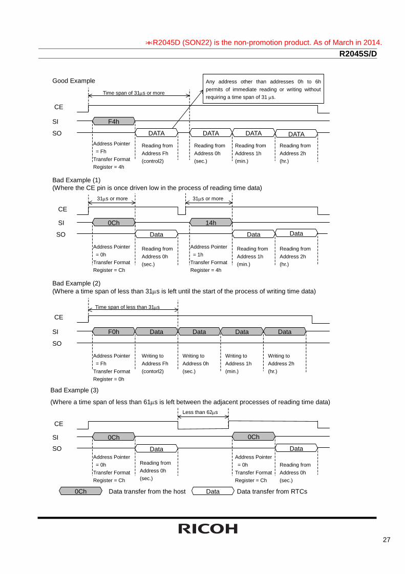
• Considerations in Reading and Writing Time Data under special condition
Any carry to the second digits in the process of reading or writing time data may cause reading or writing erroneous time data. For example, suppose a carry out of 13:59:59 into 14:00:00 occurs in the process of reading time data in the middle of shifting from the minute digits to the hour digits. At this moment, the second digits, the minute digits, and the hour digits read 59 seconds, 59 minutes, and 14 hours, respectively (indicating 14:59:59) to cause the reading of time data deviating from actual time virtually 1 hour. A similar error also occurs in writing time data. To prevent such errors in reading and writing time data, the R2045S/D has the function of temporarily locking any carry to the second digits during the high interval of the CE pin and unlocking such a carry in its high to low transition. Note that a carry to the second digits can be locked for only 1 second, during which time the CE pin should be driven low.
CE
Time counts within RTC
14:00:01
Actual time
13:59:59
Max.62μs
14:00:00
13:59:59 14:00:00 14:00:01
The effective use of this function requires the following considerations in reading and writing time data: (1) Hold the CE pin high in each session of reading or writing time data. (2) Ensure that the high interval of the CE pin lasts within 1 second. Should there be any possibility of the
host going down in the process of reading or writing time data, make arrangements in the peripheral circuitry as to drive the CE pin low or open at the moment that the host actually goes down.
(3) Leave a time span of 31μs or more from the low to high transition of the CE pin to the start of access to addresses 0h to 6h in order that any ongoing carry of the time digits may be completed within this time span.
(4) Leave a time span of 62μs or more from the high to low transition of the CE pin to its low to high transition in order that any ongoing carry of the time digits during the high interval of the CE pin may be adjusted within this time span.
The considerations listed in (1), (3), and (4) above are not required when the process of reading or writing time
data is obviously free from any carry of the time digits. (e.g. reading or writing time data in synchronization with the periodic interrupt function in the level mode or the
alarm interrupt function). Good and bad examples of reading and writing time data are illustrated on the next page.
*R2045D (SON22) is the non-promotion product. As of March in 2014.
R2045S/D
27
SO
0Ch
Data Data
Bad Example (1) (Where the CE pin is once driven low in the process of reading time data)
Less than 62μs
SO
F0h
CE Time span of less than 31μs
Writing to Address 0h (sec.)
0Ch
CE
Bad Example (3)
(Where a time span of less than 61μs is left between the adjacent processes of reading time data)
Good Example
SO DATA
F4h
DATA DATA
CE
Address Pointer = 1h Transfer Format Register = 4h
Time span of 31μs or more
Reading fromAddress 1h (min.)
DATA
SO
0Ch Data Data
31μs or more
Reading fromAddress 1h (min.)
Data
14h
31μs or more
CE
Data transfer from RTCs
0Ch
Data Data transfer from the host
Bad Example (2) (Where a time span of less than 31μs is left until the start of the process of writing time data)
Any address other than addresses 0h to 6h permits of immediate reading or writing without requiring a time span of 31 μs.
SI
SI
SI
SI
Data Data Data Data
Reading fromAddress Fh (control2)
Reading fromAddress 0h (sec.)
Reading from Address 2h (hr.)
Address Pointer = Fh Transfer Format Register = 4h
Address Pointer = Fh Transfer Format Register = 0h
Reading fromAddress 0h (sec.)
Reading from Address 2h (hr.)
Address Pointer = 0h Transfer Format Register = Ch
Writing to Address 1h (min.)
Writing to Address 2h (hr.)
Writing to Address Fh (contorl2)
Address Pointer = 0h Transfer Format Register = Ch
Reading fromAddress 0h (sec.)
Reading from Address 0h (sec.)
Address Pointer = 0h Transfer Format Register = Ch
*R2045D (SON22) is the non-promotion product. As of March in 2014.
R2045S/D
28
Correction of Time Count Deviations • The Necessity for Correction of Time Count Deviations
The oscillation frequency for R2045S/D is corrected to 0±5ppm at 25°C in fabrication. Oscillation frequency is the fastest at 25°C, (Please see Typical Characteristics Oscillation Frequency Deviation vs. Operating temperature (P.42)). In normal condition, temperature is not kept constant at 25°C. That is, R2045S/D loses without correction of time counts deviation. Generally, a clock is corrected to gain 3 to 6ppm at 25°C. R2045S/D is corrected it by setting clock adjustment register. Ricoh suggests to set 7Fh to clock adjustment register (Address 7h) for time setting to gain 3ppm at 25°C, for the equipment used indoors. And suggests to set 7Eh to clock adjustment register (Address 7h) for time setting to gain 6ppm at 25°C, for the equipment used outdoors.
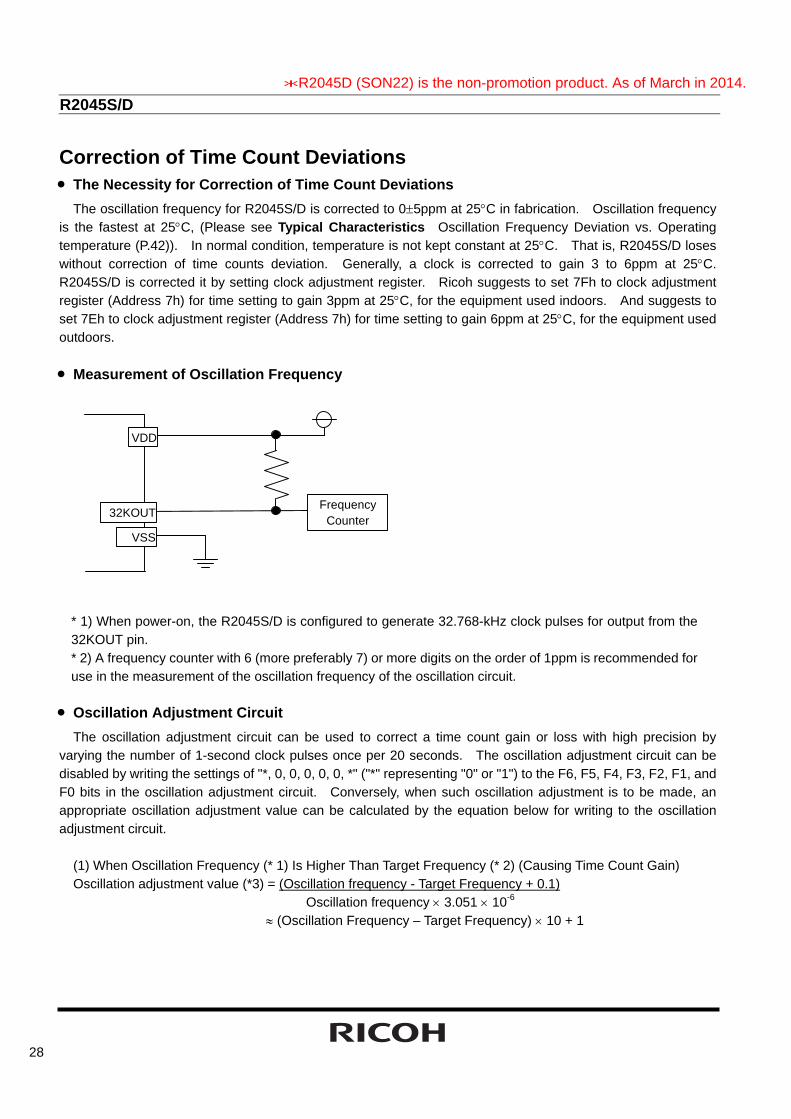
• Measurement of Oscillation Frequency
FrequencyCounter 32KOUT
VSS
VDD
* 1) When power-on, the R2045S/D is configured to generate 32.768-kHz clock pulses for output from the 32KOUT pin. * 2) A frequency counter with 6 (more preferably 7) or more digits on the order of 1ppm is recommended for use in the measurement of the oscillation frequency of the oscillation circuit.
• Oscillation Adjustment Circuit The oscillation adjustment circuit can be used to correct a time count gain or loss with high precision by
varying the number of 1-second clock pulses once per 20 seconds. The oscillation adjustment circuit can be disabled by writing the settings of "*, 0, 0, 0, 0, 0, *" ("*" representing "0" or "1") to the F6, F5, F4, F3, F2, F1, and F0 bits in the oscillation adjustment circuit. Conversely, when such oscillation adjustment is to be made, an appropriate oscillation adjustment value can be calculated by the equation below for writing to the oscillation adjustment circuit.
(1) When Oscillation Frequency (* 1) Is Higher Than Target Frequency (* 2) (Causing Time Count Gain) Oscillation adjustment value (*3) = (Oscillation frequency - Target Frequency + 0.1) Oscillation frequency × 3.051 × 10⁻⁶ ≈ (Oscillation Frequency – Target Frequency) × 10 + 1
*R2045D (SON22) is the non-promotion product. As of March in 2014.
R2045S/D
29
* 1) Oscillation frequency: Frequency of clock pulse output from the 32KOUT pin at normal temperature in the manner described in " P28 • Measurement of Oscillation Frequency". * 2) Target frequency: Desired frequency to be set. Generally, a 32.768-kHz crystal oscillator has such temperature characteristics as to have the highest oscillation frequency at normal temperature. Consequently, the crystal oscillator is recommended to have target frequency settings on the order of 32.768 to 32.76810 kHz (+3.05ppm relative to 32.768 kHz). Note that the target frequency differs depending on the environment or location where the equipment incorporating the RTC is expected to be operated. * 3) Oscillation adjustment value: Value that is to be finally written to the F0 to F6 bits in the Oscillation Adjustment Register and is represented in 7-bit coded decimal notation.
(2) When Oscillation Frequency Is Equal To Target Frequency (Causing Time Count neither Gain nor Loss) Oscillation adjustment value = 0, +1, -64, or –63 (3) When Oscillation Frequency Is Lower Than Target Frequency (Causing Time Count Loss) Oscillation adjustment value = (Oscillation frequency - Target Frequency) Oscillation frequency × 3.051 × 10⁻⁶ ≈ (Oscillation Frequency – Target Frequency) × 10 Oscillation adjustment value calculations are exemplified below (A) For an oscillation frequency = 32768.85Hz and a target frequency = 32768.05Hz Oscillation adjustment value = (32768.85 - 32768.05 + 0.1) / (32768.85 × 3.051 × 10-6) ≈ (32768.85 - 32768.05) × 10 + 1 = 9.001 ≈ 9 In this instance, write the settings ((0),F6,F5,F4,F3,F2,F1,F0)=(0,0,0,0,1,0,0,1) in the oscillation adjustment
register. Thus, an appropriate oscillation adjustment value in the presence of any time count gain represents a distance from 01h.
(B) For an oscillation frequency = 32762.22Hz and a target frequency = 32768.05Hz Oscillation adjustment value = (32762.22 - 32768.05) / (32762.22 × 3.051 × 10-6) ≈ (32762.22 - 32768.05) × 10 = -58.325 ≈ -58 To represent an oscillation adjustment value of - 58 in 7-bit coded decimal notation, subtract 58 (3Ah) from 128
(80h) to obtain 46h. In this instance, write the settings of ((0),F6,F5,F4,F3,F2,F1,F0) = (0,1,0,0,0,1,1,0) in the oscillation adjustment register. Thus, an appropriate oscillation adjustment value in the presence of any time count loss represents a distance from 80h.
Notes: 1) Oscillation adjustment does not affect the frequency of 32.768-kHz clock pulses output from the 32KOUT pin. 2) Oscillation adjustment value range: When the oscillation frequency is higher than the target frequency (causing a time count gain), an appropriate time count gain ranges from -3.05ppm to -189.2ppm with the settings of "0, 0, 0, 0, 0, 1, 0" to "0, 1, 1, 1, 1, 1, 1" written to the F6, F5, F4, F3, F2, F1, and F0 bits in the oscillation adjustment register, thus allowing correction of a time count gain of up to +189.2ppm.
*R2045D (SON22) is the non-promotion product. As of March in 2014.
R2045S/D
30
Conversely, when the oscillation frequency is lower than the target frequency (causing a time count loss), an appropriate time count gain ranges from +3.05ppm to +189.2ppm with the settings of "1, 1, 1, 1, 1, 1, 1" to "1, 0, 0, 0, 0, 1, 0" written to the F6, F5, F4, F3, F2, F1, and F0 bits in the oscillation adjustment register, thus allowing correction of a time count loss of up to -189.2ppm. 3) If following 3 conditions are completed, actual clock adjustment value could be different from target adjustment value that set by oscillator adjustment function. 1. Using oscillator adjustment function 2. Access to R2045S/D at random, or synchronized with external clock that has no relation to R2045S/D, or synchronized with periodic interrupt in pulse mode. 3. Access to R2045S/D more than 2 times per each second on average. For more details, please contact to Ricoh.
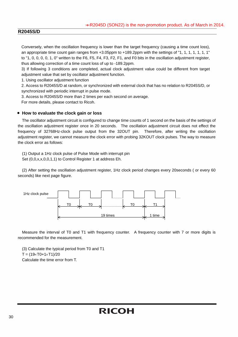
• How to evaluate the clock gain or loss The oscillator adjustment circuit is configured to change time counts of 1 second on the basis of the settings of
the oscillation adjustment register once in 20 seconds. The oscillation adjustment circuit does not effect the frequency of 32768Hz-clock pulse output from the 32OUT pin. Therefore, after writing the oscillation adjustment register, we cannot measure the clock error with probing 32KOUT clock pulses. The way to measure the clock error as follows:
(1) Output a 1Hz clock pulse of Pulse Mode with interrupt pin Set (0,0,x,x,0,0,1,1) to Control Register 1 at address Eh. (2) After setting the oscillation adjustment register, 1Hz clock period changes every 20seconds ( or every 60
seconds) like next page figure.
1Hz clock pulse
T0 T0 T0 T1
1 time19 times
Measure the interval of T0 and T1 with frequency counter. A frequency counter with 7 or more digits is
recommended for the measurement. (3) Calculate the typical period from T0 and T1 T = (19×T0+1×T1)/20 Calculate the time error from T.
*R2045D (SON22) is the non-promotion product. As of March in 2014.

R2045S/D
31
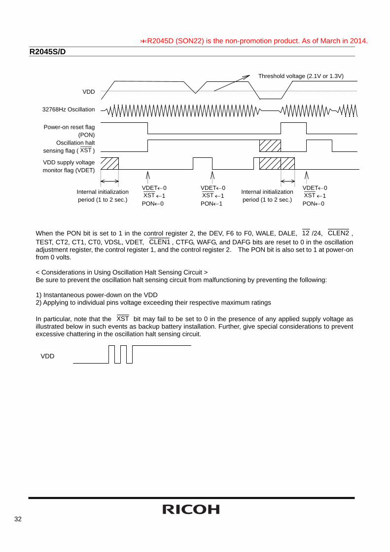
Power-on Reset, Oscillation Halt Sensing, and Supply Voltage Monitoring • PON, XST , and VDET
The power-on reset circuit is configured to reset control register1, 2, and clock adjustment register when VDD power up from 0v. The oscillation halt sensing circuit is configured to record a halt on oscillation by 32.768-kHz clock pulses. The supply voltage monitoring circuit is configured to record a drop in supply voltage below a threshold voltage of 2.1 or 1.3v.
Each function has a monitor bit. I.e. the PON bit is for the power-on reset circuit, and XST bit is for the oscillation halt sensing circuit, and VDET is for the supply voltage monitoring circuit. PON and VDET bits are activated to “H”. However, XST bit is activated to “L”. The PON and VDET accept only the writing of 0, but XST accepts the writing of 0 and 1. The PON bit is set to 1, when VDD power-up from 0V, but VDET is set to
0, and XST is indefinite. The functions of these three monitor bits are shown in the table below.
PON XST VDET Function Monitoring for the
power-on reset function Monitoring for the oscillation halt sensing function
a drop in supply voltage below a threshold voltage of 2.1 or 1.3v
Address D4 in Address Fh D5 in Address Fh D6 in Address Fh Activated High Low High When VDD power up from 0v
1 indefinite 0
accept the writing 0 only Both 0 and 1 0 only The relationship between the PON, XST , and VDET is shown in the table below.
PON XST
VDET Conditions of supply voltage and oscillation
Condition of oscillator, and back-up status
0 0 0 Halt on oscillation, but no drop in VDD supply voltage below threshold voltage
Halt on oscillation cause of condensation etc.
0 0 1 Halt on oscillation and drop in VDD supply voltage below threshold voltage, but no drop to 0V
Halt on oscillation cause of drop in back-up battery voltage
0 1 0 No drop in VDD supply voltage below threshold voltage and no halt in oscillation
Normal condition
0 1 1 Drop in VDD supply voltage below threshold voltage and no halt on oscillation
No halt on oscillation, but drop in back-up battery voltage
1 * * Drop in supply voltage to 0v Power-up from 0v,
*R2045D (SON22) is the non-promotion product. As of March in 2014.
R2045S/D
32
32768Hz Oscillation
Power-on reset flag (PON)
Oscillation halt sensing flag ( XST )
Threshold voltage (2.1V or 1.3V)
VDD
VDD supply voltage monitor flag (VDET)
Internal initialization period (1 to 2 sec.)
VDET←0 XST ←1 PON←0
VDET←0 XST ←1 PON←1
VDET←0 XST ←1 PON←0
Internal initialization period (1 to 2 sec.)
When the PON bit is set to 1 in the control register 2, the DEV, F6 to F0, WALE, DALE, 12 /24, CLEN2 , TEST, CT2, CT1, CT0, VDSL, VDET, CLEN1 , CTFG, WAFG, and DAFG bits are reset to 0 in the oscillation adjustment register, the control register 1, and the control register 2. The PON bit is also set to 1 at power-on from 0 volts. < Considerations in Using Oscillation Halt Sensing Circuit > Be sure to prevent the oscillation halt sensing circuit from malfunctioning by preventing the following: 1) Instantaneous power-down on the VDD 2) Applying to individual pins voltage exceeding their respective maximum ratings In particular, note that the XST bit may fail to be set to 0 in the presence of any applied supply voltage as illustrated below in such events as backup battery installation. Further, give special considerations to prevent excessive chattering in the oscillation halt sensing circuit.
VDD
*R2045D (SON22) is the non-promotion product. As of March in 2014.
R2045S/D
33
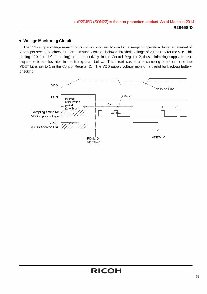
• Voltage Monitoring Circuit The VDD supply voltage monitoring circuit is configured to conduct a sampling operation during an interval of
7.8ms per second to check for a drop in supply voltage below a threshold voltage of 2.1 or 1.3v for the VDSL bit setting of 0 (the default setting) or 1, respectively, in the Control Register 2, thus minimizing supply current requirements as illustrated in the timing chart below. This circuit suspends a sampling operation once the VDET bit is set to 1 in the Control Register 2. The VDD supply voltage monitor is useful for back-up battery checking.
VDET (D6 in Address Fh)
PON
VDD 2.1v or 1.3v
1s
VDET←0
7.8ms
Sampling timing for VDD supply voltage
Internal nitiali-zation period (1 to 2sec.)
PON←0 VDET←0
*R2045D (SON22) is the non-promotion product. As of March in 2014.
R2045S/D
34
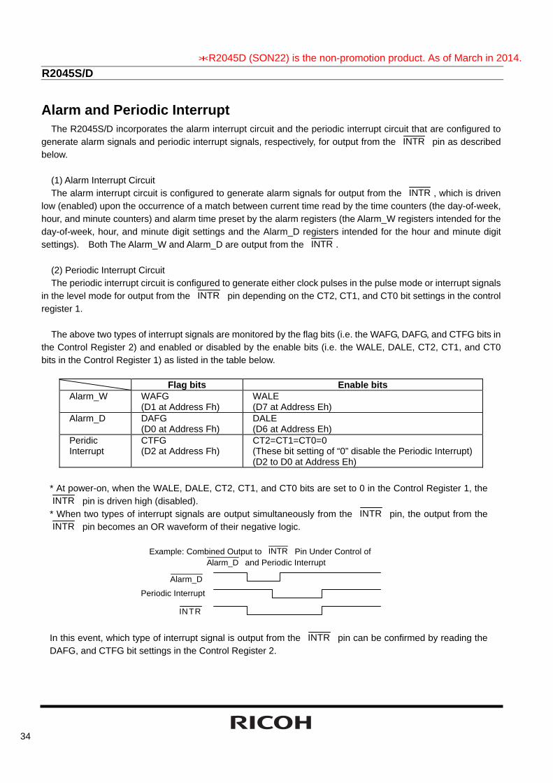
Alarm and Periodic Interrupt The R2045S/D incorporates the alarm interrupt circuit and the periodic interrupt circuit that are configured to
generate alarm signals and periodic interrupt signals, respectively, for output from the INTR pin as described below.
(1) Alarm Interrupt Circuit The alarm interrupt circuit is configured to generate alarm signals for output from the INTR , which is driven
low (enabled) upon the occurrence of a match between current time read by the time counters (the day-of-week, hour, and minute counters) and alarm time preset by the alarm registers (the Alarm_W registers intended for the day-of-week, hour, and minute digit settings and the Alarm_D registers intended for the hour and minute digit settings). Both The Alarm_W and Alarm_D are output from the INTR .
(2) Periodic Interrupt Circuit The periodic interrupt circuit is configured to generate either clock pulses in the pulse mode or interrupt signals
in the level mode for output from the INTR pin depending on the CT2, CT1, and CT0 bit settings in the control register 1.
The above two types of interrupt signals are monitored by the flag bits (i.e. the WAFG, DAFG, and CTFG bits in
the Control Register 2) and enabled or disabled by the enable bits (i.e. the WALE, DALE, CT2, CT1, and CT0 bits in the Control Register 1) as listed in the table below.
Flag bits Enable bits
Alarm_W WAFG (D1 at Address Fh)
WALE (D7 at Address Eh)
Alarm_D DAFG (D0 at Address Fh)
DALE (D6 at Address Eh)
Peridic Interrupt
CTFG (D2 at Address Fh)
CT2=CT1=CT0=0 (These bit setting of “0” disable the Periodic Interrupt) (D2 to D0 at Address Eh)
* At power-on, when the WALE, DALE, CT2, CT1, and CT0 bits are set to 0 in the Control Register 1, the INTR pin is driven high (disabled).
* When two types of interrupt signals are output simultaneously from the INTR pin, the output from the INTR pin becomes an OR waveform of their negative logic.
Example: Combined Output to INTR Pin Under Control of Alarm_D and Periodic Interrupt
Periodic Interrupt
INTR
Alarm_D
In this event, which type of interrupt signal is output from the INTR pin can be confirmed by reading the DAFG, and CTFG bit settings in the Control Register 2.
*R2045D (SON22) is the non-promotion product. As of March in 2014.
R2045S/D
35
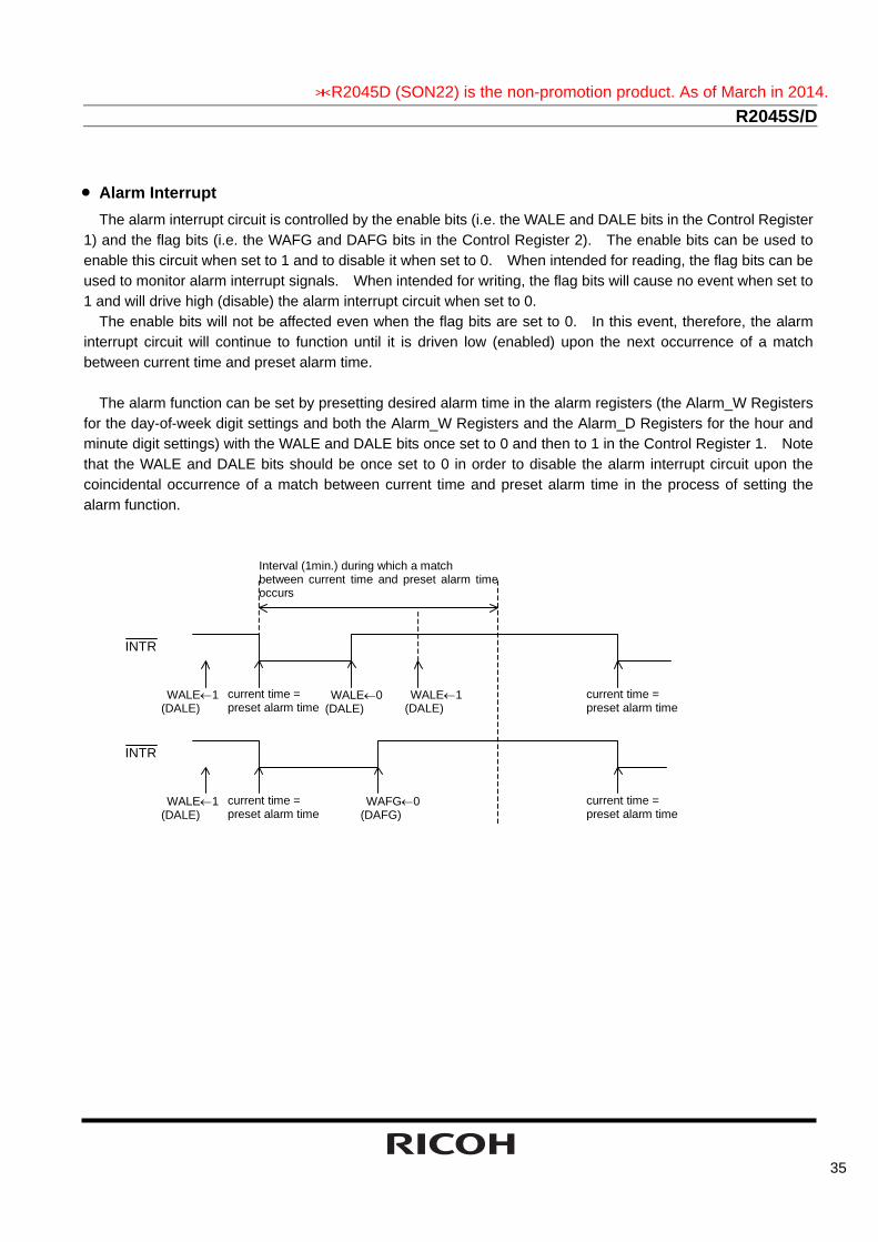
• Alarm Interrupt
The alarm interrupt circuit is controlled by the enable bits (i.e. the WALE and DALE bits in the Control Register 1) and the flag bits (i.e. the WAFG and DAFG bits in the Control Register 2). The enable bits can be used to enable this circuit when set to 1 and to disable it when set to 0. When intended for reading, the flag bits can be used to monitor alarm interrupt signals. When intended for writing, the flag bits will cause no event when set to 1 and will drive high (disable) the alarm interrupt circuit when set to 0.
The enable bits will not be affected even when the flag bits are set to 0. In this event, therefore, the alarm interrupt circuit will continue to function until it is driven low (enabled) upon the next occurrence of a match between current time and preset alarm time.
The alarm function can be set by presetting desired alarm time in the alarm registers (the Alarm_W Registers
for the day-of-week digit settings and both the Alarm_W Registers and the Alarm_D Registers for the hour and minute digit settings) with the WALE and DALE bits once set to 0 and then to 1 in the Control Register 1. Note that the WALE and DALE bits should be once set to 0 in order to disable the alarm interrupt circuit upon the coincidental occurrence of a match between current time and preset alarm time in the process of setting the alarm function.
current time = preset alarm time
WALE←1 (DALE)
Interval (1min.) during which a match between current time and preset alarm timeoccurs
current time = preset alarm time
WAFG←0(DAFG)
INTR
WALE←1(DALE)
WALE←1 (DALE)
current time = preset alarm time
WALE←0(DALE)
current time = preset alarm time
INTR
*R2045D (SON22) is the non-promotion product. As of March in 2014.
R2045S/D
36
• Periodic Interrupt
Setting of the periodic selection bits (CT2 to CT0) enables periodic interrupt to the CPU. There are two waveform modes: pulse mode and level mode. In the pulse mode, the output has a waveform duty cycle of around 50%. In the level mode, the output is cyclically driven low and, when the CTFG bit is set to 0, the output is return to High (OFF).
Description CT2 CT1 CT0
Wave form mode
Interrupt Cycle and Falling Timing
0 0 0 - OFF(H) (Default) 0 0 1 - Fixed at “L” 0 1 0 Pulse Mode *1) 2Hz(Duty50%) 0 1 1 Pulse Mode *1) 1Hz(Duty50%) 1 0 0 Level Mode *2) Once per 1 second (Synchronized with
Second counter increment)
1 0 1 Level Mode *2) Once per 1 minute (at 00 seconds of every Minute)
1 1 0 Level Mode *2) Once per hour (at 00 minutes and 00 Seconds of every hour)
1 1 1 Level Mode *2) Once per month (at 00 hours, 00 minutes, and 00 seconds of first day of every month)
*1) Pulse Mode: 2-Hz and 1-Hz clock pulses are output in synchronization with the increment of the second counter as illustrated in the timing chart below.
INTR Pin
Rewriting of the second counter
CTFG Bit
Approx. 92μs
(Increment of second counter) In the pulse mode, the increment of the second counter is delayed by approximately 92 μs from the falling edge of clock pulses. Consequently, time readings immediately after the falling edge of clock pulses may appear to lag behind the time counts of the real-time clocks by approximately 1 second. Rewriting the second counter will reset the other time counters of less than 1 second, driving the INTR pin low. *2) Level Mode: Periodic interrupt signals are output with selectable interrupt cycle settings of 1 second, 1 minute, 1 hour, and 1 month. The increment of the second counter is synchronized with the falling edge of periodic interrupt signals. For example, periodic interrupt signals with an interrupt cycle setting of 1 second are output in synchronization with the increment of the second counter as illustrated in the timing chart below.
*R2045D (SON22) is the non-promotion product. As of March in 2014.
R2045S/D
37
CTFG Bit
INTR Pin
Setting CTFG bit to 0 Setting CTFG bit to 0
(Increment of
second counter) (Increment of
second counter) (Increment of
second counter)
*1), *2) When the oscillation adjustment circuit is used, the interrupt cycle will fluctuate once per 20sec. as follows: Pulse Mode: The “L” period of output pulses will increment or decrement by a maximum of ±3.784ms. For example, 1-Hz clock pulses will have a duty cycle of 50 ±0.3784%. Level Mode: A periodic interrupt cycle of 1 second will increment or decrement by a maximum of ±3.784 ms.
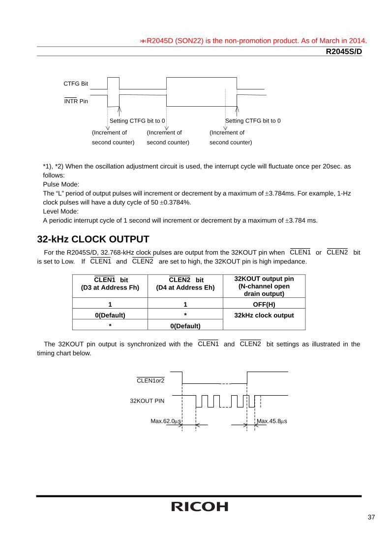
32-kHz CLOCK OUTPUT For the R2045S/D, 32.768-kHz clock pulses are output from the 32KOUT pin when CLEN1 or CLEN2 bit
is set to Low. If CLEN1 and CLEN2 are set to high, the 32KOUT pin is high impedance.
CLEN1 bit (D3 at Address Fh)
CLEN2 bit (D4 at Address Eh)
32KOUT output pin (N-channel open
drain output) 1 1 OFF(H)
0(Default) * * 0(Default)
32kHz clock output
The 32KOUT pin output is synchronized with the CLEN1 and CLEN2 bit settings as illustrated in the
timing chart below.
32KOUT PIN
Max.62.0μs
CLEN1or2
Max.45.8μs
*R2045D (SON22) is the non-promotion product. As of March in 2014.
R2045S/D
38
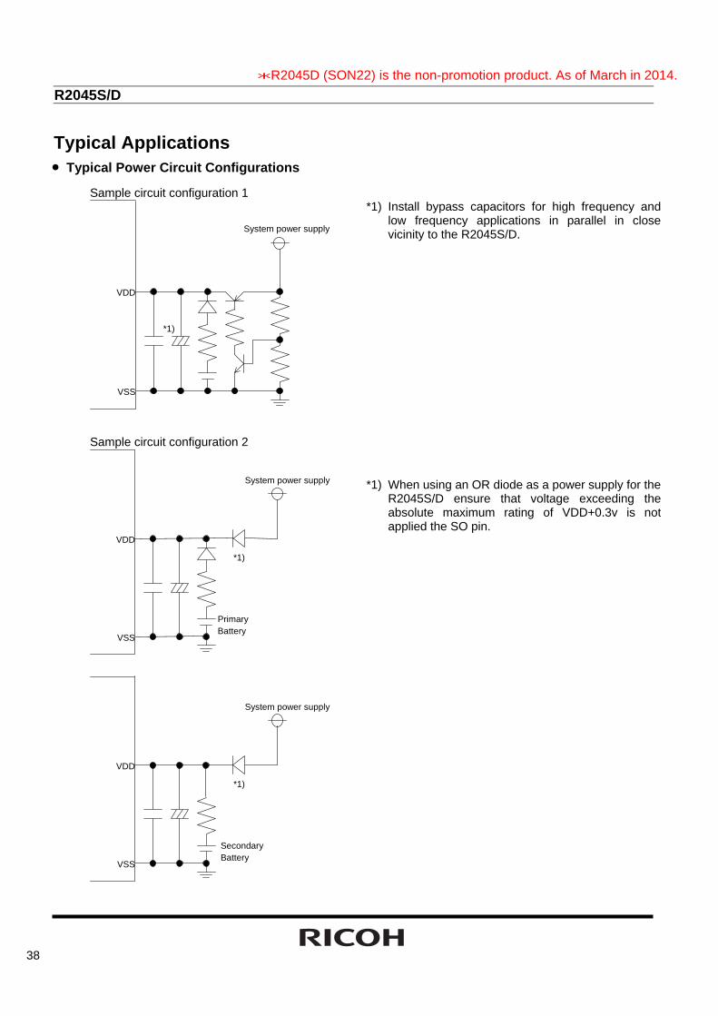
Typical Applications • Typical Power Circuit Configurations
Sample circuit configuration 1
VDD
VSS
System power supply
*1)
Sample circuit configuration 2
*1)
VSS
System power supply
VDD
Primary Battery
*1)
VSS
System power supply
VDD
Secondary Battery
*1) Install bypass capacitors for high frequency and low frequency applications in parallel in close vicinity to the R2045S/D.
*1) When using an OR diode as a power supply for the R2045S/D ensure that voltage exceeding the absolute maximum rating of VDD+0.3v is not applied the SO pin.
*R2045D (SON22) is the non-promotion product. As of March in 2014.

R2045S/D
39
• Connection of INTR Pin The INTR pin follows the N-channel open drain output logic and contains no protective diode on the power
supply side. As such, it can be connected to a pull-up resistor of up to 5.5 volts regardless of supply voltage.
VDD
INTR *1)B
A
Backup power supply
System power supply
VSS
• Connection of 32KOUT Pin
The 32KOUT pin follows the Nch. open drain output and contains no protective diode on the power supply side. As such, it can be connected to a device with a supply voltage of up to 5.5 volts regardless of supply voltage, provided that such connection involves considerations for the supply current requirements of a pull-up resistor, which can be roughly calculated by the following equation:
I = 0.5 × (VDD or VCC) / Rp
VDD
32KOUT *1)B
A
Backup power supply
System power supply
VSS
*1) Depending on whether the INTR pin is tobe used during battery backup, it should beconnected to a pull-up resistor at the followingdifferent positions:
(1) Position A in the left diagram when it is not tobe used during battery backup.
(2) Position B in the left diagram when it is to beused during battery backup.
*1) Depending on whether the 32KOUT pin isto be used during battery backup, it shouldbe connected to a pull-up resistor at thefollowing different positions:
(1) Position A in the left diagram when it is notto be used during battery backup.
(2) Position B in the left diagram when it is tobe used during battery backup.
*R2045D (SON22) is the non-promotion product. As of March in 2014.
R2045S/D
40
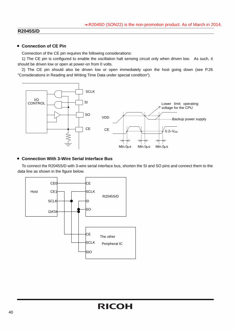
• Connection of CE Pin Connection of the CE pin requires the following considerations: 1) The CE pin is configured to enable the oscillation halt sensing circuit only when driven low. As such, it
should be driven low or open at power-on from 0 volts. 2) The CE pin should also be driven low or open immediately upon the host going down (see P.26
"Considerations in Reading and Writing Time Data under special condition").
I/OCONTROL
SO
SCLK
CE
SI
CE
Min.0μs
VDD
Lower limit operating voltage for the CPU
Min.0μs Min.0μs
0.2×VDD
Backup power supply
• Connection With 3-Wire Serial Interface Bus To connect the R2045S/D with 3-wire serial interface bus, shorten the SI and SO pins and connect them to the
data line as shown in the figure below.
CE The other
Peripheral IC
CE1
SCLK
DATA
Host
SCLK
SIO
SO
CE0 CE
SCLK
SI R2045S/D
*R2045D (SON22) is the non-promotion product. As of March in 2014.
R2045S/D
41
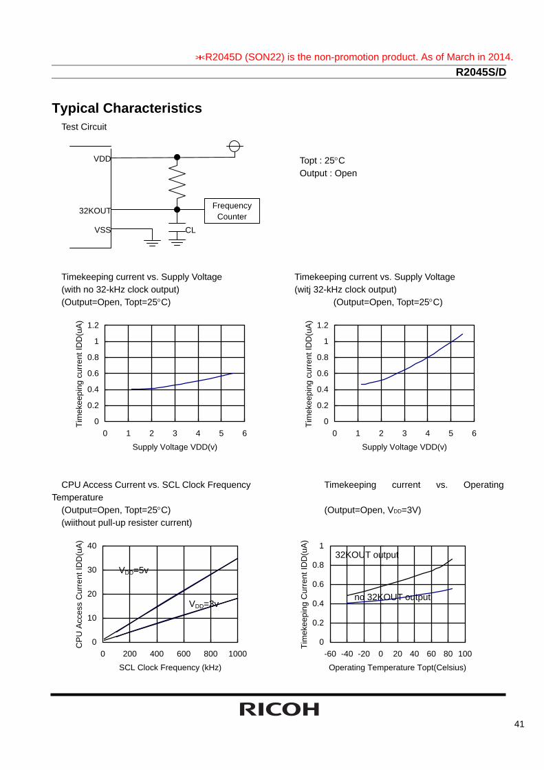
Typical Characteristics Test Circuit
FrequencyCounter
VDD
32KOUT
VSS CL
Timekeeping current vs. Supply Voltage Timekeeping current vs. Supply Voltage (with no 32-kHz clock output) (witj 32-kHz clock output) (Output=Open, Topt=25°C) (Output=Open, Topt=25°C)
0
0.2
0.4
0.6
0.8
1
1.2
0 1 2 3 4 5 6Supply Voltage VDD(v)
Tim
ekee
ping
cur
rent
IDD
(uA
)
0
0.2
0.4
0.6
0.8
1
1.2
0 1 2 3 4 5 6Supply Voltage VDD(v)
Tim
ekee
ping
cur
rent
IDD
(uA
)
CPU Access Current vs. SCL Clock Frequency Timekeeping current vs. Operating
Temperature (Output=Open, Topt=25°C) (Output=Open, VDD=3V) (wiithout pull-up resister current)
0
10
20
30
40
0 200 400 600 800 1000SCL Clock Frequency (kHz)
CP
U A
cces
s C
urre
nt ID
D(u
A)
0
0.2
0.4
0.6
0.8
1
-60 -40 -20 0 20 40 60 80 100Operating Temperature Topt(Celsius)
Tim
ekee
ping
Cur
rent
IDD
(uA
)
VDD=5v
VDD=3v
Topt : 25°C Output : Open
32KOUT output
no 32KOUT output
*R2045D (SON22) is the non-promotion product. As of March in 2014.

R2045S/D
42
Oscillation Frequency Deviation vs. Supply Voltage Oscillation Frequency Deviation vs. (Topt=25°C) Operating Temperature (VDD=3v)
-5-4-3-2-1012345
0 1 2 3 4 5 6
Power Supply VDD (v)
Osc
illatio
n Fr
eque
ncy
Dev
iatio
n (p
pm)
-120
-100
-80
-60
-40
-20
0
20
-60 -40 -20 0 20 40 60 80 100
Operating Temperature Topt(Celsius)O
scilla
tion
frequ
ency
Dev
iatio
n (p
pm)
VOL vs. IOL( INTR pin) VOL vs. IOL( INTR pin) (Topt=25°C) (VIN=VDD,Topt=25°C)
0
5
10
15
20
25
30
35
0 0.2 0.4 0.6 0.8 1
VOL (v)
IOL
(mA
)
0
5
10
15
20
25
30
35
0 0.2 0.4 0.6 0.8 1
VOL (v)
IOL
(mA
)
Oscillation Start Time vs. Power Supply (Topt=25°C)
0
100
200
300
400
500
0 1 2 3 4 5 6
Power Supply VDD (v)
Osc
illatio
n S
tart
Tim
e (m
s)
VDD=5v VDD=3v
*R2045D (SON22) is the non-promotion product. As of March in 2014.
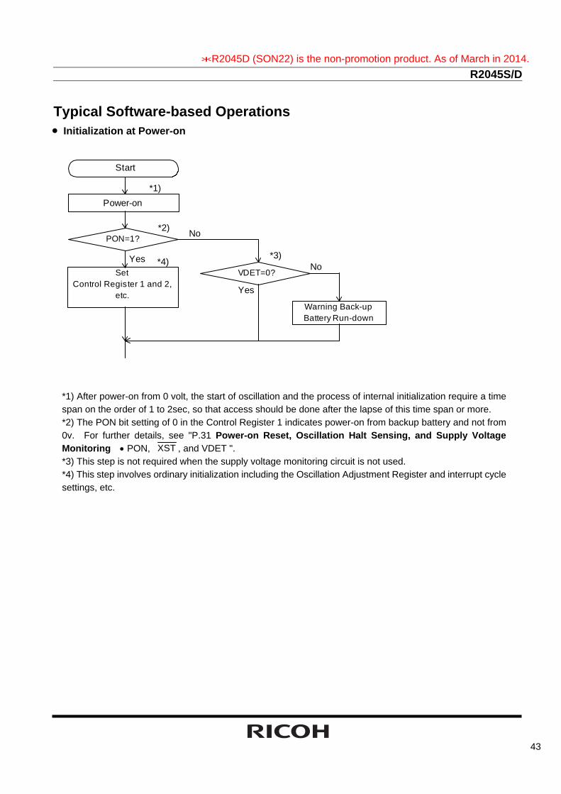
R2045S/D
43
Typical Software-based Operations • Initialization at Power-on
Start
*1)
Yes
NoVDET=0?
Warning Back-upBattery Run-down
SetControl Register 1 and 2,
etc.
Power-on
*2)
*4)*3)
PON=1?
Yes
No
*1) After power-on from 0 volt, the start of oscillation and the process of internal initialization require a time span on the order of 1 to 2sec, so that access should be done after the lapse of this time span or more. *2) The PON bit setting of 0 in the Control Register 1 indicates power-on from backup battery and not from 0v. For further details, see "P.31 Power-on Reset, Oscillation Halt Sensing, and Supply Voltage Monitoring • PON, XST , and VDET ". *3) This step is not required when the supply voltage monitoring circuit is not used. *4) This step involves ordinary initialization including the Oscillation Adjustment Register and interrupt cycle settings, etc.
*R2045D (SON22) is the non-promotion product. As of March in 2014.

R2045S/D
44
• Writing of Time and Calendar Data
Write to Time Counter and Calendar Counter
*2)
CE←L *1)
CE ← H *1)
Write to Clock Adjustment Register
*3)
• Reading Time and Calendar Data (1) Ordinary Process of Reading Time and Calendar Data
Read from Time Counter and Calendar Counter
*1) CE ← L
CE ← H *1)
*1) When writing to clock and calendar counters, do not drive CE to L until all times from second to year have been written to prevent error inwriting time. For more detailed in "P.25 Considerations in Readingand Writing Time Data under special condition".
*2) Any writing to the second counter will reset divider units lower than thesecond digits.
*3) Please see “P,27 The Necessity for Correction of Time CountDeviations”
The R2045S/D may also be initialized not at power-on but in the
process of writing time and calendar data.
*1) When reading clock and calendar counters, do not drive CE to L untilall times from second to year have been written to prevent error inwriting time. For more detailed in "P.25 Considerations in Readingand Writing Time Data under special condition".
*R2045D (SON22) is the non-promotion product. As of March in 2014.
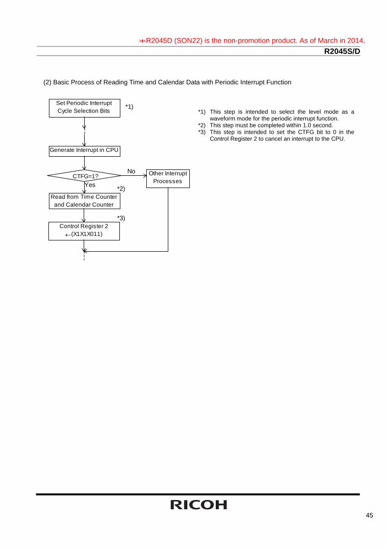
R2045S/D
45
(2) Basic Process of Reading Time and Calendar Data with Periodic Interrupt Function
*2)
Other InterruptProcesses
Set Periodic InterruptCycle Selection Bits
CTFG=1?
Read from Time Counterand Calendar Counter
Yes
No
Control Register 2←(X1X1X011)
Generate Interrupt in CPU
*1)
*3)
*1) This step is intended to select the level mode as awaveform mode for the periodic interrupt function.
*2) This step must be completed within 1.0 second. *3) This step is intended to set the CTFG bit to 0 in the
Control Register 2 to cancel an interrupt to the CPU.
*R2045D (SON22) is the non-promotion product. As of March in 2014.
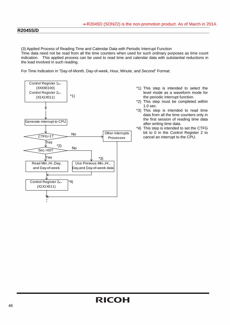
R2045S/D
46
(3) Applied Process of Reading Time and Calendar Data with Periodic Interrupt Function Time data need not be read from all the time counters when used for such ordinary purposes as time count indication. This applied process can be used to read time and calendar data with substantial reductions in the load involved in such reading. For Time Indication in "Day-of-Month, Day-of-week, Hour, Minute, and Second" Format:
*2)
Other interruptsProcesses
Control Register 1←(XXXX0100)
Control Register 2←(X1X1X011)
Sec.=00?
Yes
No
Use Previous Min.,Hr.,Day,and Day-of-week data
Generate interrupt to CPU
*1)
*3)
CTFG=1?
Control Register 2←(X1X1X011)
Yes
Read Min.,Hr.,Day,and Day-of-week
*4)
No
*1) This step is intended to select thelevel mode as a waveform mode forthe periodic interrupt function.
*2) This step must be completed within1.0 sec.
*3) This step is intended to read timedata from all the time counters only inthe first session of reading time dataafter writing time data.
*4) This step is intended to set the CTFGbit to 0 in the Control Register 2 tocancel an interrupt to the CPU.
*R2045D (SON22) is the non-promotion product. As of March in 2014.
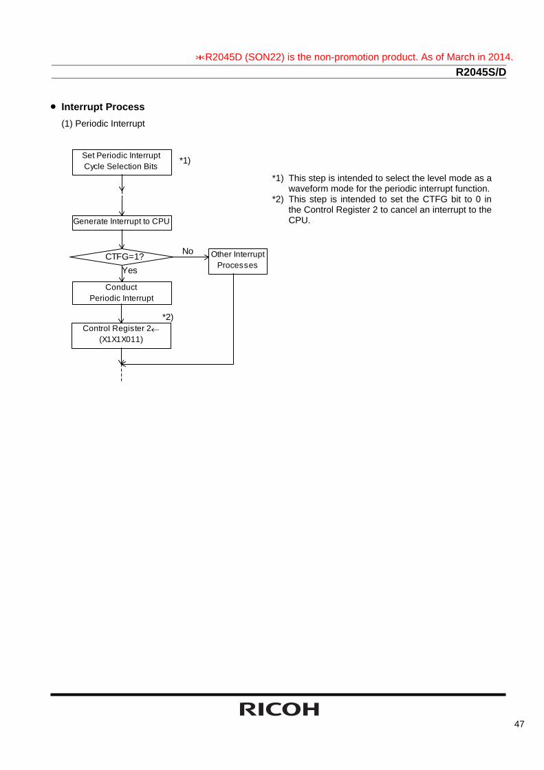
R2045S/D
47
• Interrupt Process (1) Periodic Interrupt
*2)
Other InterruptProcesses
Set Periodic InterruptCycle Selection Bits
CTFG=1?
ConductPeriodic Interrupt
Yes
No
Control Register 2←(X1X1X011)
Generate Interrupt to CPU
*1)
*1) This step is intended to select the level mode as a waveform mode for the periodic interrupt function.
*2) This step is intended to set the CTFG bit to 0 in the Control Register 2 to cancel an interrupt to the CPU.
*R2045D (SON22) is the non-promotion product. As of March in 2014.
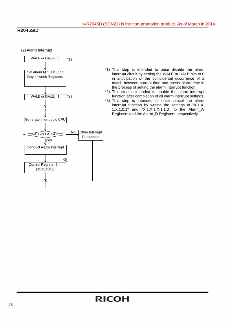
R2045S/D
48
(2) Alarm Interrupt
*3)
Other InterruptProcesses
Set Alarm Min., Hr., andDay-of-week Registers
WAFG or DAFG=1?
Conduct Alarm Interrupt
Yes
No
Control Register 2 ←(X1X1X101)
Generate Interrupt to CPU
*1)
WALE or DALE←1
WALE or DALE←0
*2)
*1) This step is intended to once disable the alarminterrupt circuit by setting the WALE or DALE bits to 0in anticipation of the coincidental occurrence of amatch between current time and preset alarm time inthe process of setting the alarm interrupt function.
*2) This step is intended to enable the alarm interruptfunction after completion of all alarm interrupt settings.
*3) This step is intended to once cancel the alarminterrupt function by writing the settings of "X,1,X,1,X,1,0,1" and "X,1,X,1,X,1,1,0" to the Alarm_WRegisters and the Alarm_D Registers, respectively.
*R2045D (SON22) is the non-promotion product. As of March in 2014.
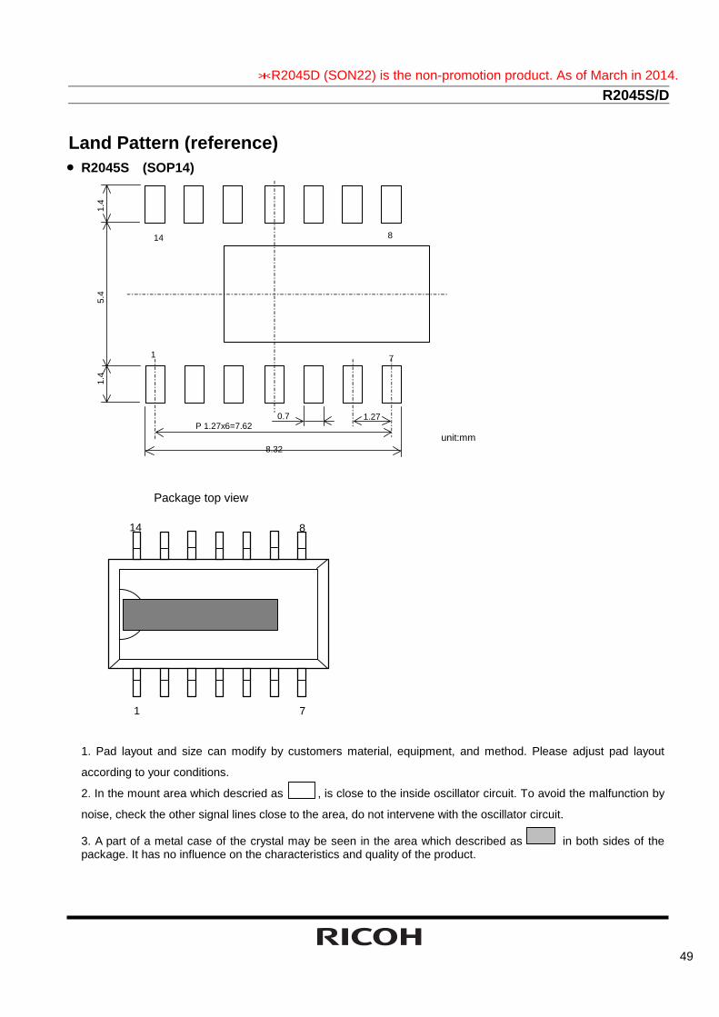
R2045S/D
49
Land Pattern (reference) • R2045S (SOP14)
8
0.7 1.27
1 7
8.32
P 1.27x6=7.62
14
5.4
1.4
1.4
unit:mm
Package top view
14
1 7
8
1. Pad layout and size can modify by customers material, equipment, and method. Please adjust pad layout
according to your conditions.
2. In the mount area which descried as , is close to the inside oscillator circuit. To avoid the malfunction by
noise, check the other signal lines close to the area, do not intervene with the oscillator circuit. 3. A part of a metal case of the crystal may be seen in the area which described as in both sides of thepackage. It has no influence on the characteristics and quality of the product.
*R2045D (SON22) is the non-promotion product. As of March in 2014.
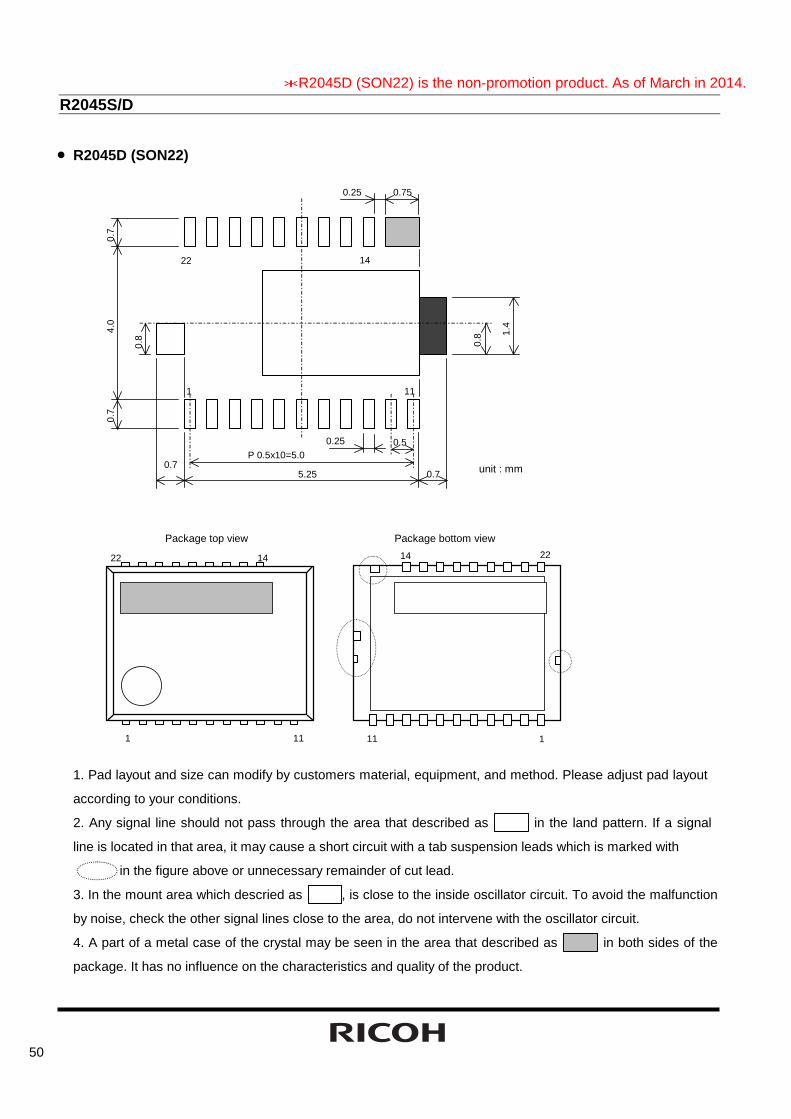
R2045S/D
50
• R2045D (SON22)
0.7
14
0.25 0.5
1 11
0.75.25
P 0.5x10=5.0
0.8 0.8 1.
4
0.25 0.75
22
4.0
0.7
0.7
unit : mm
Package top view Package bottom view 22
11 1
1422 14
1 11
1. Pad layout and size can modify by customers material, equipment, and method. Please adjust pad layout
according to your conditions.
2. Any signal line should not pass through the area that described as in the land pattern. If a signal
line is located in that area, it may cause a short circuit with a tab suspension leads which is marked with
in the figure above or unnecessary remainder of cut lead.
3. In the mount area which descried as , is close to the inside oscillator circuit. To avoid the malfunction
by noise, check the other signal lines close to the area, do not intervene with the oscillator circuit.
4. A part of a metal case of the crystal may be seen in the area that described as in both sides of the
package. It has no influence on the characteristics and quality of the product.
*R2045D (SON22) is the non-promotion product. As of March in 2014.

http://www.e-devices.ricoh.co.jp/en/
Sales & Support OfficesRICOH ELECTRONIC DEVICES CO., LTD.Higashi-Shinagawa Office (International Sales)3-32-3, Higashi-Shinagawa, Shinagawa-ku, Tokyo 140-8655, JapanPhone: +81-3-5479-2857 Fax: +81-3-5479-0502
RICOH EUROPE (NETHERLANDS) B.V.Semiconductor Support CentreProf. W.H. Keesomlaan 1, 1183 DJ Amstelveen, The Netherlands Phone: +31-20-5474-309
RICOH ELECTRONIC DEVICES KOREA CO., LTD.3F, Haesung Bldg, 504, Teheran-ro, Gangnam-gu, Seoul, 135-725, KoreaPhone: +82-2-2135-5700 Fax: +82-2-2051-5713
RICOH ELECTRONIC DEVICES SHANGHAI CO., LTD.Room 403, No.2 Building, No.690 Bibo Road, Pu Dong New District, Shanghai 201203, People's Republic of ChinaPhone: +86-21-5027-3200 Fax: +86-21-5027-3299
RICOH ELECTRONIC DEVICES CO., LTD.Taipei officeRoom 109, 10F-1, No.51, Hengyang Rd., Taipei City, Taiwan (R.O.C.)Phone: +886-2-2313-1621/1622 Fax: +886-2-2313-1623
Ricoh is committed to reducing the environmental loading materials in electrical deviceswith a view to contributing to the protection of human health and the environment. Ricoh has been providing RoHS compliant products since April 1, 2006 and Halogen-free products since April 1, 2012.Halogen Free
1. The products and the product specifications described in this document are subject to change or discontinuation of production without notice for reasons such as improvement. Therefore, before deciding to use the products, please refer to Ricoh sales representatives for the latest information thereon.
2. The materials in this document may not be copied or otherwise reproduced in whole or in part without prior written consent of Ricoh.
3. Please be sure to take any necessary formalities under relevant laws or regulations before exporting or otherwise taking out of your country the products or the technical information described herein.
4. The technical information described in this document shows typical characteristics of and example application circuits for the products. The release of such information is not to be construed as a warranty of or a grant of license under Ricoh's or any third party's intellectual property rights or any other rights.
5. The products listed in this document are intended and designed for use as general electronic components in standard applications (office equipment, telecommunication equipment, measuring instruments, consumer electronic products, amusement equipment etc.). Those customers intending to use a product in an application requiring extreme quality and reliability, for example, in a highly specific application where the failure or misoperation of the product could result in human injury or death (aircraft, spacevehicle, nuclear reactor control system, traffic control system, automotive and transportation equipment, combustion equipment, safety devices, life support system etc.) should first contact us.
6. We are making our continuous effort to improve the quality and reliability of our products, but semiconductor products are likely to fail with certain probability. In order to prevent any injury to persons or damages to property resulting from such failure, customers should be careful enough to incorporate safety measures in their design, such as redundancy feature, fire containment feature and fail-safe feature. We do not assume any liability or responsibility for any loss or damage arising from misuse or inappropriate use of the products.
7. Anti-radiation design is not implemented in the products described in this document.8. Please contact Ricoh sales representatives should you have any questions or comments concerning the products or the technical information.
Related Documents