DIGITAL COMMUNICATIONS LABORATORY MA NU AL (R13) III – B. Tech., II-Semester ECE DEPARTMENT OF ELECTRONICS AND COMMUNICATION ENGINEERING RAMACHANDRA COLLEGE OF ENGINEERING, ELURU – 534 007 Accredited by NAAC with “ B ++” Grade (Approved by AICTE, New Delhi & Affiliated to JNTUK: Kakinada) West Godavari District, Andhra Pradesh

Welcome message from author
This document is posted to help you gain knowledge. Please leave a comment to let me know what you think about it! Share it to your friends and learn new things together.
Transcript
DIGITAL COMMUNICATIONS
LABORATORY MANUAL
(R13) III – B. Tech., II-Semester
ECE
DEPARTMENT OF ELECTRONICS AND COMMUNICATION ENGINEERING
RAMACHANDRA COLLEGE OF ENGINEERING, ELURU – 534 007
Accredited by NAAC with “B++” Grade
(Approved by AICTE, New Delhi & Affiliated to JNTUK: Kakinada) West Godavari District, Andhra Pradesh
RCE DIGITAL COMMUNICATIONS LAB
DEPARTMENT OF ELECTRONICS & COMMUNICATION ENGINEERING 2
DIGITAL COMUNICATIONS LAB
(R13) III – B. Tech., ECE II- Semester
Index
S. No. Name of the Experiment
1. Time division multiplexing.
2. Pulse code modulation.
3. Differential pulse code modulation.
4. Delta modulation.
5. Frequency shift keying.
6. Phase shift keying
7. Differential phase shift keying.
8. Companding
9. Source Encoder and Decoder
10. Linear Block Code-Encoder and Decoder
11. Binary Cyclic Code - Encoder and Decoder
12. Convolution Code - Encoder and Decoder
Experiments Beyond the syllabus Using MATLAB
13. Companding
14. ASK
15. Minimum Shift Keying (MSK)
RCE DIGITAL COMMUNICATIONS LAB
DEPARTMENT OF ELECTRONICS & COMMUNICATION ENGINEERING 3
GENERAL INSTRUCTIONS:
1. The experiments have been designed to be performed within the 3-hour
laboratory time.
2. To successfully complete the experiment in one lab turn, come prepared to
the laboratory.
3. Read the experiment in advance.
4. List and collect the components for the experiment.
5. Be sure that the specifications and values of the components are as per
design.
6. Follow the experimental steps judiciously.
7. Record stepwise observations using proper test instruments.
8. Get the observation signed by the instructor.
9. Always take safety precautions while performing experiments.
GUIDANCE FOR THE LABORATORY REPORT:
1. Format of the report
Exp. No: Expt. Title: Date:
Objective:
List of instruments and components:
Theory in brief
Procedure, Observations, Graph if any
Result
2. Write the experimental observations and measurements stepwise.
3. Plot the graph neatly. Always label the axes and indicate units too. Wherever
frequency response is to be drawn, use the semi-log graph paper.
4. Compare the results with theoretical values with remarks/comments.
5. Wherever necessary, sketch the circuit diagram neatly and label the components.
.
RCE DIGITAL COMMUNICATIONS LAB
DEPARTMENT OF ELECTRONICS & COMMUNICATION ENGINEERING 4
1. TIME DIVISION MULTIPLEXING
AIM: To study the characteristics of Time Division Multiplexing and Demultiplexing
EQUIPMENT REQUIRED:
1. TDM Multiplexer & De-Multiplexer trainer
2. Digital Storage Oscilloscope
3. Digital Multimeter.
4. 2 No’s co-axial cables (standard accessories with trainer)
Note: Storage oscilloscope is desired for satisfactory observation of TDM wave
forms
THEORY:
Time Division Multiplexing enables the joint utilization of a single channel by
different message signals without mutual interference. The important feature of
Pulse Amplitude Modulation is conservation of time. This can be achieved by using
Time Division Multiplexing. That is for a given message signal, transmission of the
associated PAM wave engages the communication channel for only a fraction of the
sampling interval on a periodic basis. Hence, some of the time interval between
adjacent pulses of the PAM wave is cleared for use by other independent message
signals on a time shared basis.
In TDM each input signal is first passed through low pass filter in order to
restrict the bandwidth. The pre – alias filter is then applied to a commutator, which
is usually implemented using electronic switching circuitry. The function of
commutator is twofold: (1) To take a narrow sample of each of the N input
messages at a rate 𝑓𝑠 that is slightly higher than 2𝑊 , where 𝑊 is the cutoff
frequency of the pre – alias filter, and (2) To sequentially interleave these N samples
inside a sampling interval 𝑇𝑠 = 1/𝑓𝑠. Indeed, this latter function is the essence of the
time division multiplexing operation. The multiplexed signal is then appl ied to a
Pulse Amplitude Modulator, the purpose of which is to transform the multiplexed
signal into a form suitable for transmission over the communication channel.
RCE DIGITAL COMMUNICATIONS LAB
DEPARTMENT OF ELECTRONICS & COMMUNICATION ENGINEERING 5
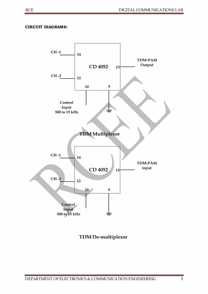
CIRCUIT DIAGRAMS:

RCE DIGITAL COMMUNICATIONS LAB
DEPARTMENT OF ELECTRONICS & COMMUNICATION ENGINEERING 6
PROCEDURE:
Multiplexer:
1. Study the theory of operation.
2. Connect the trainer TDM Multiplexer to the mains and switch on the power
supply.
3. Measure the output of the regulated power supply i.e. +5 V and -5 V with the
help of digital multimeter.
4. Observe the output of the AF generator-1 using CRO; it should be a Sine
wave of 400 Hz frequency with 3 𝑉𝑝−𝑝amplitude.
5. Observe the output of the AF generator-2 using CRO it should be a Sine
wave of 200 Hz frequency with 3 𝑉𝑝−𝑝 amplitude.
6. Verify the operation of logic source with multimeter/scope, output should be
+5 V in logic1 position and 0 V in logic "0" position.
7. Observe the output of the Clock generator using CRO; it should be a Square
wave of 500 Hz to 15 kHz frequency with 5 𝑉𝑝−𝑝amplitude.
8. Now connect the CH 1 & CH 2 Inputs of the TDM multiplexer to the outputs
of the AF Generator 1 and 2 respectively.
9. Connect Control input of the TDM multiplexer to the output of the logic
source.
10. Put control signal (logic source) at logic 1 condition and observe the output
of the TDM multiplexer with the help oscilloscope, by this we can notice that
the output of the TDM multiplexer is a signal which has been connected to
CH1 input. In this condition the signal at CH 2 input has no effect on
multiplexer output.
11. Similarly put logic source at logic 0 position and observe the output of the
TDM multiplexer. Now notice that the output of the TDM multiplexer is a
signal which has been connected to the CH 2 input and the signal at CH 1
input has no effect on multiplexer output.
12. Now disconnect logic source and connect clock output to the control input.
13. Observe TDM wave form using CRO at different values of clock frequency,
input signal voltage levels and sketch them.
RCE DIGITAL COMMUNICATIONS LAB
DEPARTMENT OF ELECTRONICS & COMMUNICATION ENGINEERING 7
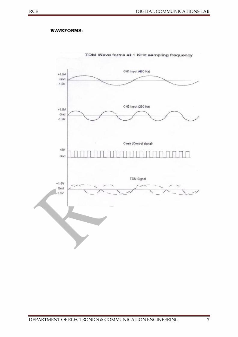
WAVEFORMS:

RCE DIGITAL COMMUNICATIONS LAB
DEPARTMENT OF ELECTRONICS & COMMUNICATION ENGINEERING 8
Note1: After setting the clock frequency and input signals to desire values
put storage scope in STOP mode so that you can view stable display of
waveforms.
Note2: Sample wave forms given in Figures are drawn at 1 kHz sampling
clock, you can take at any clock frequency.
Similarly you can observe and plot the TDM waveforms for different inputs i.e. DC
signals alone, AC & DC instead of AC signals.
Note1: DC Signals (voltages) can be connected from an external sources and
care should be taken in case voltage levels i.e. maximum voltage input
voltage must be in range of ± 4.8 V.
Note2: You can use even normal scope, when you observe the TDM wave
form for DC inputs.
De-multiplexer:
1. Study the theory of operation.
2. Connect the trainer TDM DE-multiplexer to the mains and switch on the
power supply.
3. Measure the output of the regulated power supply i.e. +5 V and -5 V with the
help of digital multimeter.
4. Verify the operation of logic source with multimeter/scope, output should be
+5 V in logic "1" position and 0 V in logic 0 position.
5. Observe the output of the Clock generator using CRO; it should be a Square
wave of 500 Hz to 15 kHz frequency with 5 Vp amplitude.
6. Connect TDM-PAM signal to input of TDM de-multiplexer from TDM
multiplexer with the help of co-axial cable (supplied with trainer).
7. Connect control input to logic source output.
8. Keep CRO in dual mode; connect one input to CH 1 output and another
input to CH 2 output.
9. Put logic source to 1 position and observe CH 1 and CH 2 outputs. You can
notice that the entire TDM signal is transferred to CH 1 output and has no
signal at CH 2 output.
10. Similarly put logic source to "0" positions and observe CH 1 and CH 2
outputs. Now the entire TDM signal is transferred to CH 2 output and has
no signal at CH 1 output. By the above two steps you can notice that the
RCE DIGITAL COMMUNICATIONS LAB
DEPARTMENT OF ELECTRONICS & COMMUNICATION ENGINEERING 9
entire TDM signal is transferred to CH 1 output when control input is "1"
and to CH 2 output when control input is "0".
11. Now disconnect logic source and connect clock from the transmitter (i.e.,
AET- 55M) through a coaxial cable.
12. Observe CH 1 and CH 2 outputs. You will notice that the outputs are
natural top sampled PAM signals.
13. Connect CH 1, CH 2 outputs to low pass filters and observe the output of the
filters and compare them with the original AF Signals ( at multiplexer inputs)
using CRO. You will notice that both the signals are same in frequency and
shape. Signal amplitude may be attenuated during smoothing process and
this can be achieved by taking amplifiers output. Select AC/DC coupling
depending on the input signal.
Observation on effect of synchronization:
Disconnect clock from multiplexer (AET-55M) and connect to local oscillator (i.e.,
clock generator output from AET-55D) with remaining setup as it is. Observe CH 1
and CH 2 outputs and compare them with the previous results. These signals are
little bit distorted in shape. This is because lack of synchronization between clock
at multiplexer and clock at de-multiplexer. You can get further perfection in output
wave forms by adjusting the locally generated clock.
RESULT:
VIVA QUESTIONS:
1. Define Multiplexing.
2. Define bandwidth.
3. Define synchronization.
4. What is the purpose of pre – alias filter?
5. What is the purpose of commutator?
6. Define Nyquist rate.
7. Define cross talk.
8. What is the purpose of reconstruction filters?
9. What are the applications of Time Division Multiplexing?
10. Define equalization in TDM.
RCE DIGITAL COMMUNICATIONS LAB
DEPARTMENT OF ELECTRONICS & COMMUNICATION ENGINEERING 10
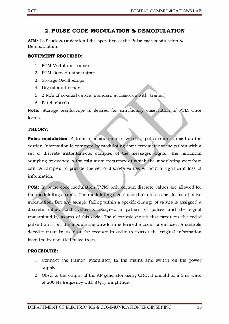
2. PULSE CODE MODULATION & DEMODULATION
AIM: To Study & understand the operation of the Pulse code modulation &
Demodulation.
EQUIPMENT REQUIRED:
1. PCM Modulator trainer
2. PCM Demodulator trainer
3. Storage Oscilloscope
4. Digital multimeter
5. 2 No’s of co-axial cables (standard accessories with trainer)
6. Patch chords
Note: Storage oscilloscope is desired for satisfactory observation of PCM wave
forms
THEORY:
Pulse modulation: A form of modulation in which a pulse train is used as the
carrier. Information is conveyed by modulating some parameter of the pulses with a
set of discrete instantaneous samples of the messages signal. The minimum
sampling frequency is the minimum frequency at which the modulating waveform
can be sampled to provide the set of discrete values without a significant loss of
information.
PCM: In pulse code modulation (PCM) only certain discrete values are allowed for
the modulating signals. The modulating signal sampled, as in other forms of pulse
modulation. But any sample falling within a specified range of values is assigned a
discrete value. Each value is assigned a pattern of pulses and the signal
transmitted by means of this code. The electronic circuit that produces the coded
pulse train from the modulating waveform is termed a coder or encoder. A suitable
decoder must be used at the receiver in order to extract the original information
from the transmitted pulse train.
PROCEDURE:
1. Connect the trainer (Modulator) to the mains and switch on the power
supply.
2. Observe the output of the AF generator using CRO; it should be a Sine wave
of 200 Hz frequency with 3 𝑉𝑃−𝑃 amplitude.
RCE DIGITAL COMMUNICATIONS LAB
DEPARTMENT OF ELECTRONICS & COMMUNICATION ENGINEERING 11
3. Verify the output of the DC source with multimeter / scope, output should
vary from 0 to +5 V.
4. Observe the output of the Clock generator using CRO, they should be 64
kHz and 4 kHz frequency of square wave with 5 𝑉𝑃−𝑃 amplitude.
CIRCUIT DIAGRAMS:
RCE DIGITAL COMMUNICATIONS LAB
DEPARTMENT OF ELECTRONICS & COMMUNICATION ENGINEERING 12
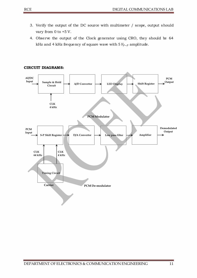
WAVEFORMS:
Note: These clock signals are internally connected the circuit so no external
connections are required.
5. Connect the trainer (De Modulator) to the mains and switch on the power
supply.
6. Observe the output of the clock generator using CRO; it should be 64 kHz
square wave with 5 𝑉𝑃−𝑃 amplitude.
PCM OPERATION (WITH DC INPUT)
MODULATION:
1. Set DC source to some value say 1 V with the help of multimeter and
connect it to the A/D converter input and observe the output LED’s.
2. Note down the digital code i.e., output of the A/D converter and compare
with the theoretical value.
Theoretical value can be obtained by:
A/D input voltage ________________ = 𝑋(10) = 𝑌 2 1 𝐿𝑆𝐵 𝑉𝑎𝑙𝑢𝑒
Where
1 LSB value = 𝑉𝑟𝑒𝑓 2𝑛 , Since 𝑉𝑟𝑒𝑓 = 5 𝑉 𝑎𝑛𝑑 𝑛 = 8
1 LSB Value = 0.01953
Example:
A/D input voltage = 1 V = 51.2(10) = 00110011(2)
So digital output is 00110011
RCE DIGITAL COMMUNICATIONS LAB
DEPARTMENT OF ELECTRONICS & COMMUNICATION ENGINEERING 13
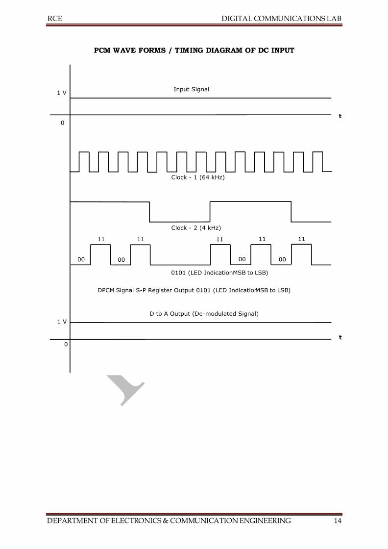
Keep CRO in dual mode. Connect one channel to 4 kHz signal ( which is connected
to the shift register) and another channel to the PCM output. Observe the PCM
output with respect to the 4 kHz signal and sketch the waveforms. Compare them
with the given waveforms
Note: From this wave form you can observe that the LSB bit enters the output first.
DEMODULATION:
1. Connect PCM signal to the demodulators (S-P Shift register) from the PCM
modulator with help of coaxial cable (supplied with the trainer).
2. Connect clock signal (64 kHz) from the transmitter to the receiver using
coaxial cable.
3. Connect transmitter clock to the timing circuit.
4. Observe and note down the S-P shift register output data and compare it
with the transmitted data (i.e., output A/D converter at transmitter.
RCE DIGITAL COMMUNICATIONS LAB
DEPARTMENT OF ELECTRONICS & COMMUNICATION ENGINEERING 14
PCM WAVE FORMS / TIMING DIAGRAM OF DC INPUT
RCE DIGITAL COMMUNICATIONS LAB
DEPARTMENT OF ELECTRONICS & COMMUNICATION ENGINEERING 15
notice that the output of the S-P shift register is following the A/D converter
output in the modulator. Observe D/A converter output (demodulated
output) using multimeter /scope and compare it with the original signal and
you can observe that there is no loss in information in process of conversion
and transmission.
5. Similarly you can try for different values of modulating signal voltage.
SAMPLE WORK SHEET:
1. Modulating signal : 1 V
2. A/D output (theoretical) : 00 11 00 11(2)
3. A/D output (practical) : 00 11 00 11(2)
4. S-P output : 00 11 00 11(2)
5. D/A Converter output : 1 V(Demodulation output)
PCM OPERATION (WITH AC INPUT):
MODULATION:
1. Connect AC signal of 2 𝑉𝑃−𝑃 amplitude to Sample & Hold circuit.
2. Keep the CRO in dual mode. Connect one channel to the AF signal and
another channel to the sample & hold output. Observe and sketch the
sample & hold output.
3. Connect the sample and hold output to the A/D converter and observe the
PCM output using storage oscilloscope/ DTO.
4. Observe PCM output by varying AF signal voltage.
DEMODULATION:
1. Connect PCM signal to the demodulator input (S-P shift register) from the
PCM modulator with the help of coaxial cable (supplied with the trainer)
2. Connect clock signal (64 kHz) from the transmitter to the receiver using
coaxial cable
3. Connect transmitter clock to the timing circuit.
4. Keep CRO in dual mode. Connect CH 1 input to the sample and hold output
and CH 2 input of the D/A converter output.
5. Observe and sketch the D/A output.
6. Connect D/A output to the LPF input.
RCE DIGITAL COMMUNICATIONS LAB
DEPARTMENT OF ELECTRONICS & COMMUNICATION ENGINEERING 16
7. Observe output of the LPF/Amplifier and compare it with the original
modulating signal.
8. From above observation you can verify that there is no loss in information
(modulating signal) in conversion and transmission process.
9. Disconnect clock from transmitter and connect to local oscillator (i.e., clock
generator output from Demodulator) with remaining setup as it is. Observe
D/A output and compare it with the previous result. This signal is little bit
distorted in shape. This is because lack of synchronization between clock at
transmitter and clock at receiver.
Note: You can take modulating signals from external sources. Maximum amplitude
should not exceed 4 V in case of DC and 3 𝑉𝑃−𝑃in case of AC (AF)
signals.
RESULT:
VIVA QUESTIONS?
1. Define modulation.
2. What are three different processing steps in PCM?
3. Define signal – to – noise ratio.
4. Define quantization error.
5. Define overload level.
6. What is ternary code?
7. What are advantages of PCM?
8. Define White Gaussian noise.
9. Define channel and Quantization noise.
10. What are three basic functions of Regenerative repeaters?
RCE DIGITAL COMMUNICATIONS LAB
DEPARTMENT OF ELECTRONICS & COMMUNICATION ENGINEERING 17
3. DIFFERENTIAL PULSE CODE MODULATION
AIM: To Study & understand the operation of the DPCM
EQUIPMENT REQUIRED:
1. DPCM Modulator & Demodulator trainer
2. Storage Oscilloscope
3. Digital Multimeter
4. 2 No’s of co- axial cables (standard accessories with trainer)
5. Patch chords
THEORY:
Differential PCM is quite similar to ordinary PCM. However, each word in this
system indicates the difference in amplitude, positive or negative, between this
sample and the previous sample. Thus the relative value of each sample is
indicated rather than, the absolute value as in normal PCM.
PROCEDURE:
1. Study the theory of operation thoroughly.
2. Connect the trainer (Modulator) to the mains and switch on the power
supply.
3. Observe the output of the AF generator using CRO; it should be Sine wave
of 400 Hz frequency with 3 𝑉𝑝−𝑝 amplitude.
4. Verify the output of the DC source with multimeter/scope; output should
vary 0 to +290 mV.
5. Observe the output of the Clock generator using CRO, they should be 64
kHz and 8 kHz frequency of square with 5 𝑉𝑝−𝑝 amplitude.
6. Connect the trainer (De Modulator) to the mains and switch on the power
supply.
7. Observe the output of the Clock generator using CRO; it should be 64 kHz
square wave with amplitude of 5𝑉𝑝−𝑝
DPCM OPERATION (WITH DC INPUT):
MODULATION:
1. Keep CRO in dual mode. Connect one channel to 8 kHz signal (one which is
connected to the Shift register) and another channel to the DPCM output.
RCE DIGITAL COMMUNICATIONS LAB
DEPARTMENT OF ELECTRONICS & COMMUNICATION ENGINEERING 18
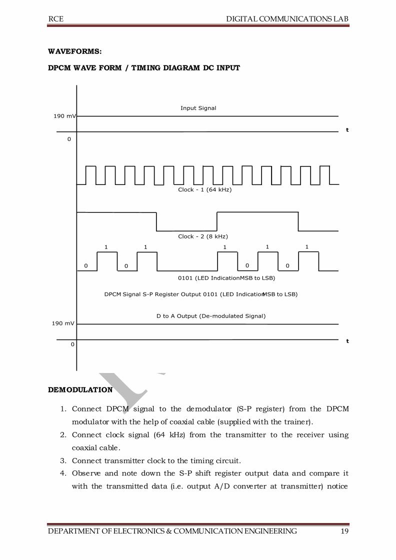
2. Observe the DPCM output with respect to the 8 kHz signal and sketch the
waveforms.
Note: Form this waveform you can observe that the LSB bit enters the output first.
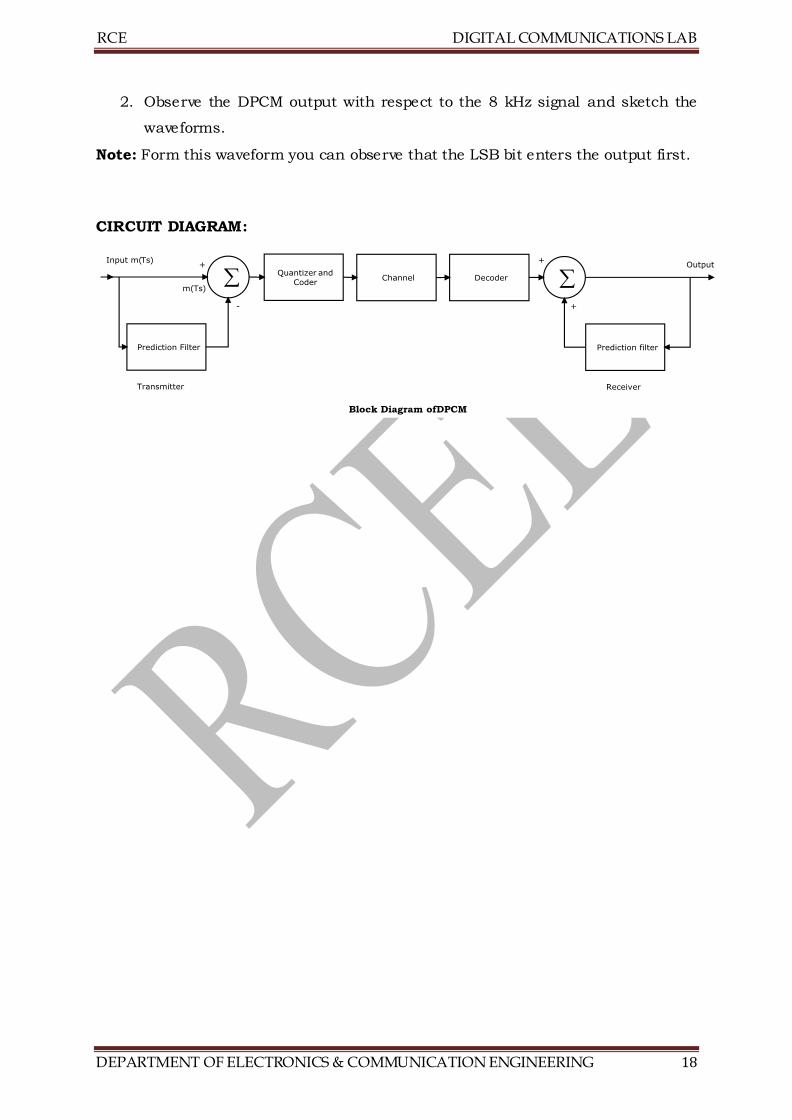
CIRCUIT DIAGRAM:
RCE DIGITAL COMMUNICATIONS LAB
DEPARTMENT OF ELECTRONICS & COMMUNICATION ENGINEERING 19
WAVEFORMS:
DPCM WAVE FORM / TIMING DIAGRAM DC INPUT
DEMODULATION
1. Connect DPCM signal to the demodulator (S-P register) from the DPCM
modulator with the help of coaxial cable (supplied with the trainer).
2. Connect clock signal (64 kHz) from the transmitter to the receiver using
coaxial cable.
3. Connect transmitter clock to the timing circuit.
4. Observe and note down the S-P shift register output data and compare it
with the transmitted data (i.e. output A/D converter at transmitter) notice
RCE DIGITAL COMMUNICATIONS LAB
DEPARTMENT OF ELECTRONICS & COMMUNICATION ENGINEERING 20
that the output of the S-P shift register is following the A/D converter output
in the modulator.
5. Observe D/A converter output (demodulated output) using
multimeter/scope and compare it with the original signal and can observe
that there is no loss in information in process of conversion and
transmission.
DPCM OPERATION (WITH AC INPUT):
MODULATION:
1. Connect AC signal of 3VPP amplitude to positive terminal of the summer
circuit.
Note: The output of the prediction filter is connected to the negative terminal of
the summer circuit and can observe the waveforms at the test points
provided on the board.
2. The output of the summer is internally connected to the sample and hold
circuit
3. Keep CRO in dual mode. Connect one channel to the AF signal and another
channel to the Sample and Hold output. Observe and sketch the sample &
hold output
4. Connect the Sample and Hold output to the A/D converter and observe the
DPCM output using oscilloscope.
5. Observe DPCM output by varying AF signal voltage.
DEMODULATION:
1. Connect DPCM signal to the demodulator input (S-P shift register) from the
DPCM modulator with the help of coaxial cable.
2. Connect clock signal (64 kHz) from the transmitter to the receiver using
coaxial cable.
3. Connect transmitter clock to the timing circuit.
4. Keep CRO in dual mode. Connect one channel to the sample & hold output
and another channel to the D/A converter output.
5. Observe and sketch the D/A output
6. Connect D/A output to the LPF input and observe the output of the LPF.
7. Observe the wave form at the output of the summer circuit.
RCE DIGITAL COMMUNICATIONS LAB
DEPARTMENT OF ELECTRONICS & COMMUNICATION ENGINEERING 21
8. Disconnect clock from transmitter and connect to the local oscillator (i.e.,
clock generator output from De-Modulator) with remaining setup as it is.
Observe D/A output and compare it with the previous result. This signal is
little bit distorted in shape. This is because lack of synchronization between
clock at transmitter and clock at receiver.
RESULT:
VIVA QUESTIONS:
1. Define modulation.
2. Define DPCM.
3. What is advantage of DPCM over PCM?
4. What is the purpose of predictor in DPCM?
5. Define quantizing.
6. Define encoding.
7. What are the applications of DPCM?
8. Define Signal – to – noise ratio.
9. Define prediction error
10. Define Nyquist rate.
RCE DIGITAL COMMUNICATIONS LAB
DEPARTMENT OF ELECTRONICS & COMMUNICATION ENGINEERING 22
4. DELTA MODULATION & DEMODULATION
AIM: To study the characteristics of Delta Modulation and Demodulation.
EQUIPMENT REQUIRED:
1. DM Modulator & Demodulator trainer
2. Storage Oscilloscope
3. Digital multimeter.
4. 2 No’s co-axial cables (standard accessories with trainer)
Note: Storage oscilloscope is desired for satisfactory observation of DM wave forms
THEORY:
Delta modulation is almost similar to differential PCM. In this, only one bit is
transmitted per sample just to indicate whether the present sample is larger or
smaller than the previous one. The encoding, decoding and quantizing process
become extremely simple but this system cannot handle rapidly varying samples.
This increases quantizing noise. It has also not found wide acceptance.
PROCEDURE:
DM Modulator:
1. Study the theory of operation.
2. Connect the trainer (DM Modulator) to the mains and switch on the power
supply.
3. Observe the output of the AF generator using CRO; it should be a Sine wave
of 100 Hz frequency with 3 𝑉𝑝−𝑝amplitude.
4. Verify the output of the DC source with multimeter/scope; output should
vary 0 to +4 V.
5. Observe the output of the Clock generator using CRO, they should be 4 kHz
frequency of square wave with 5 𝑉𝑝−𝑝 amplitude.
Note: This clock signal isinternally connected to the up/down counter so no external coion is required
DM with DC Voltage as modulating signal:
1. Connect dc signal from the DC source to the inverting input of the
comparator and set some voltage say 3 V.
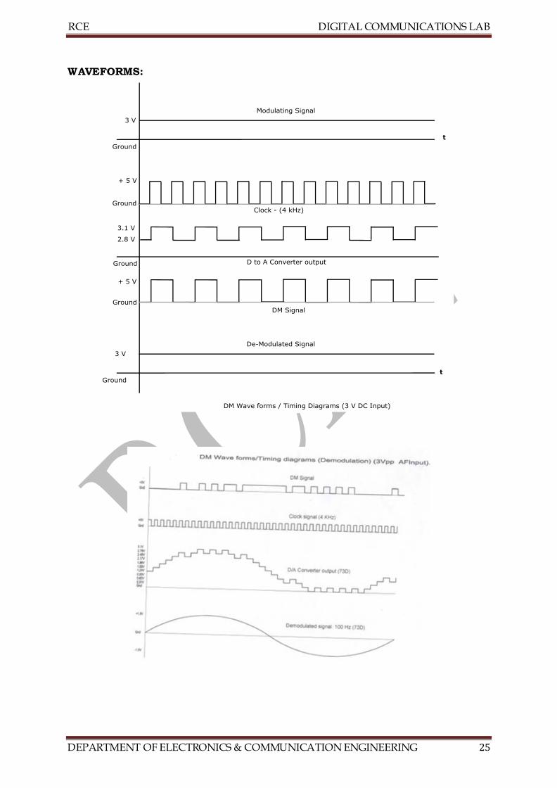
2. Observe and plot the signals at D/A converter output (i.e., non-inverting
input of the comparator), DM signal using CRO and compare them with the
wave forms given in figure.
RCE DIGITAL COMMUNICATIONS LAB
DEPARTMENT OF ELECTRONICS & COMMUNICATION ENGINEERING 23
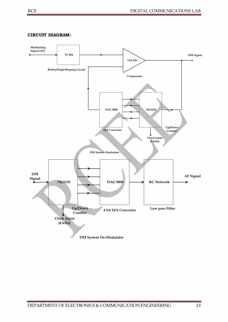
CIRCUIT DIAGRAM:
RCE DIGITAL COMMUNICATIONS LAB
DEPARTMENT OF ELECTRONICS & COMMUNICATION ENGINEERING 24
3. Connect DM signal (from Modulator) to the DM input of the demodulator.
4. Connect clock (4 kHz) from modulator to the clock input of the demodulator.
Connect clock input of the UP/DOWN counter to the clock from transmitter
with the help of springs provided.
5. Observe digital output (LED Indication) of the UP/DOWN counter and
compare it with the output of the UP/DOWN. By this you can notice that the
both the outputs are same.
6. Observe and plot the output of the D/A converter and compare it with the
wave forms given in Figure.
7. Measure the demodulated signal (i.e., output of the D/A converter with the
help of multimeter and compare it with the original signal.
8. From above observation you can notice that the both the voltages are equal
and there is no loss in process of modulation, transmission and
demodulation.
9. Similarly you can verify the DM operation for different values of modulating
signal.
DM With AF signals as modulating signal:
1. Connect AF signal from AF generator to the inverting input of the
comparator and set output amplitude at 3 𝑉𝑝−𝑝.
2. Observe and plot the signals at D/A converter output (i.e., non-inverting
input of the comparator), DM signal using CRO and compare them with the
wave forms given in figure.
3. Connect DM signal to the DM input of the demodulator.
4. Connect clock (4 kHz) from modulator to the clock input of the demodulator.
Connect clock input of the UP/DOWN counter to the clock from transmitter
with the help of springs provided.
5. Observe and plot the output of the D/A converter and compare it with the
wave forms given in Figure.
6. Observe and sketch the D/A output.
7. Connect D/A output to the LPF input.
8. Observe the output of the LPF/Amplifier and compare it with the original
modulating signal.
RCE DIGITAL COMMUNICATIONS LAB
DEPARTMENT OF ELECTRONICS & COMMUNICATION ENGINEERING 25
WAVEFORMS:
RCE DIGITAL COMMUNICATIONS LAB
DEPARTMENT OF ELECTRONICS & COMMUNICATION ENGINEERING 26
RESULT:
VIVA QUESTIONS?
1. Define modulation.
2. Define Delta modulation.
3. What are two unique features of Delta modulation?
4. What are the applications of Delta modulation?
5. What is the purpose of accumulator in DM?
6. What are differences between DM and DPCM?
7. What is the purpose of low pass filter?
8. Define bandwidth.
9. Define quantization noise.
10. Define slope overload distortion.

RCE DIGITAL COMMUNICATIONS LAB
DEPARTMENT OF ELECTRONICS & COMMUNICATION ENGINEERING 27
5. FREQUENCY SHIFT KEYING
AIM: To study the characteristics of Frequency Shift keying.
EQUIPMENT REQUIRED:
1. Frequency Shift Keying system trainer
2. Dual trace Oscilloscope
3. Digital multimeter
4. Digital frequency counter
THEORY:
Frequency Shift Keying (FSK) is a modulation/ Data transmitting
technique in which carrier frequency is shifted between two distinct fixed
frequencies to represent logic 1 and logic 0. The low carrier frequency
represents a digital 0 (space) and higher carrier frequency is a 1 (mark). FSK
system has a wide range of applications in low speed digital data transmission
systems. Wave forms are shown in Figure. FSK Modulating & Demodulating
circuitry can be developed in number of ways, familiar VCO and PLL circuits
are used in this trainer.
PROCEDURE:
1. Connect the trainer to mains and switch on the power supply.
2. Measure the output voltage of the regulated power supply i.e. +12 V with the
help of digital multimeter.
3. Verify the operation of the logic source using digital multimeter. Output
should be zero volts in Logic 0 position and 12 V in logic 1 position.
4. Observe the output of the data signal using Oscilloscope. It should be a
square wave of 20 Hz to 180 Hz @ 10 𝑉𝑝−𝑝 . (For frequency variation
potentiometer is provided)
FSK Modulation:
1. Connect output of the logic source to data input of the FSK Modulator.
2. Set logic source switch in 0 positions.
3. Connect FSK modulator output to Oscilloscope as well as frequency counter.
4. Set the output frequency of the FSK modulator as per your desire (say 1.2
kHz) with the help of control F0 which represents logic 0.
5. Set logic source switch in 1 position.
RCE DIGITAL COMMUNICATIONS LAB
DEPARTMENT OF ELECTRONICS & COMMUNICATION ENGINEERING 28
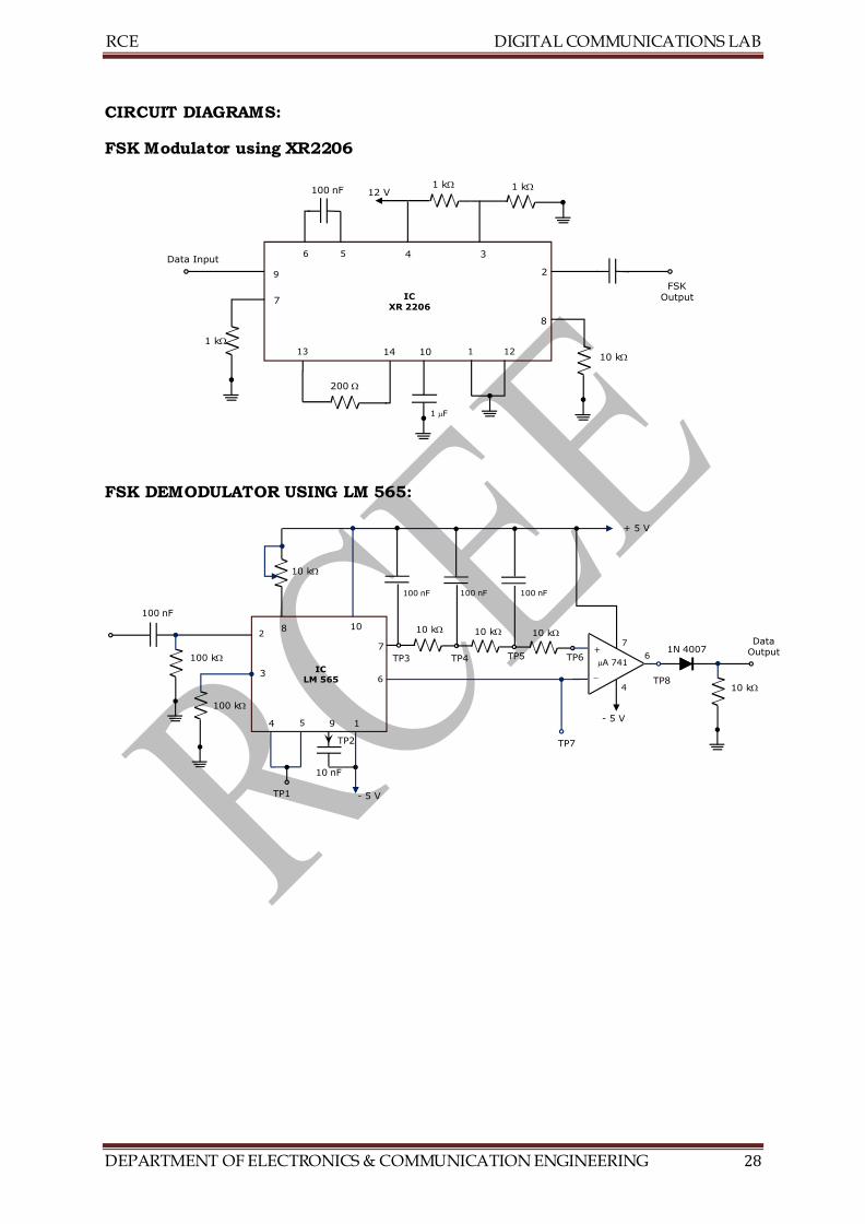
CIRCUIT DIAGRAMS:
FSK Modulator using XR2206
FSK DEMODULATOR USING LM 565:
RCE DIGITAL COMMUNICATIONS LAB
DEPARTMENT OF ELECTRONICS & COMMUNICATION ENGINEERING 29
6. Set the output frequency of the FSK modulator as per your desire (say 2.4
kHz) with the help of control F1 which represents logic 1.
Note: We have chosen F0 as 1.2 kHz and F1 as 2.4 kHz for ease of operation;
in fact you may set any value.
7. Now connect data input of the FSK modulator to the output of the data
signal generator.
8. Keep CRO in dual mode connect CH1 input of the oscilloscope to the input
of the FSK modulator and CH2 input to the output of the FSK modulator.
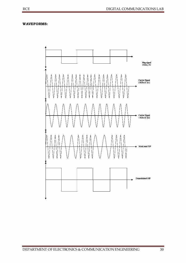
9. Observe the FSK signal for different data signal frequencies and plot them.
By this we can observe that the carrier frequency is shifting between two
predetermined frequencies as per the data signal i.e. 1.2 kHz when data
signal is 0 and 2.4 kHz when data input is 1 in this case.
10. Compare these plotted wave forms with the theoretically drawn in figure.
FSK Demodulation:
1. Again connect input of the FSK modulator to the logic source and put data
source switch in 0 positions.
2. Connect the frequency counter to the output of the FSK modulator output.
3. Set FSK output frequency to 2025 Hz with the help of FO control.
4. Now put data source switch in 1 position and set the FSK output frequency
to 2225 Hz with the help of F1 control without disturbing the F0.
Note: As per one of the standards, for proper demodulation of FSK signal the F0
should be 2025 Hz and F1 should be 2225 Hz.
1. Disconnect the FSK input of the modulator from logic source and connect
to the data signal generator.
2. Observe the output of the modulator using CRO and compare them with
given waveforms in figure.
3. Now connect the FSK modulator output to the FSK input of the
demodulator.
4. Connect CH1 input of the Oscilloscope to the data signal at modulator and
CH2 input to the output of the FSK demodulator (keep CRO in dual mode).
5. Observe and plot the output of the FSK demodulator for different
frequencies of data signal. Compare the original data signal and
demodulated signal; by this we can observe that there is no loss in process
of FSK modulation and de-modulation.
RCE DIGITAL COMMUNICATIONS LAB
DEPARTMENT OF ELECTRONICS & COMMUNICATION ENGINEERING 30
WAVEFORMS:
RCE DIGITAL COMMUNICATIONS LAB
DEPARTMENT OF ELECTRONICS & COMMUNICATION ENGINEERING 31
RESULT:
VIVA QUESTIONS:
1. What is meant by digital modulation technique?
2. Define FSK.
3. What is other name for binary FSK?
4. What are coherent FSK and non – coherent FSK?
5. Define M – ary modulation.
6. What is VCO and what is the purpose of VCO in FSK?
7. Which component refers LM 565?
8. What are applications of FSK?
9. What are the advantages of FSK over ASK?
10. What is the difference between FSK and MSK?
RCE DIGITAL COMMUNICATIONS LAB
DEPARTMENT OF ELECTRONICS & COMMUNICATION ENGINEERING 32
6. PHASE SHIFT KEYING
AIM: To study the operation of PSK (Binary) Modulation & Demodulation and to
plot the PSK wave forms for Binary data at different frequencies.
EQUIPMENT REQUIRED:
1. Phase Shift keying trainer
2. Dual trace Oscilloscope
3. Digital multimeter
4. Patch chords
THEORY:
Phase Shifting Keying (PSK) is a modulating / Data transmitting technique
in which phase of the carrier signal is shifted between two distinct levels. In a
simple PSK (i.e., Binary PSK) un-shifted carrier 𝑽𝒄𝒐𝒔𝝎𝟎𝒕 is transmitted to indicate a
1 condition, and the carrier shifted by 𝟏𝟖𝟎𝒐 i.e., −𝑽𝒄𝒐𝒔𝝎𝟎𝒕 is transmitted to indicate
a 0 condition. Wave forms are shown in Figure PSK Modulating & Demodulating
circuitry can be developed in number of ways; one of the simple circuits is used in
this trainer.
PROCEDURE:
1. Study the theory of operation.
2. Connect the trainer to mains and switch on the power supply.
3. Measure the output of the regulated power supply i.e. +5 V and -5 V with the
help of digital multimeter.
4. Observe the output of the carrier generator using CRO, it should be an 8 kHz
Sine with 𝟓 𝑽𝒑−𝒑 amplitude.
5. Observe the various data signals (1 kHz, 2 kHz and 4 kHz) using CRO.
MODULATION
1. Connect carrier signal to carrier input of the PSK Modulator.
2. Connect data signal say 4 kHz from data source to data input of the
modulator.
3. Keep CRO in dual mode.
4. Connect CH1 input of the CRO to data signal and CH2 to the output of the
PSK modulator
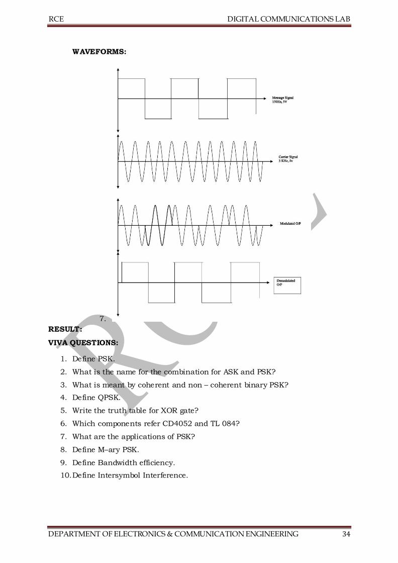
5. Observe the PSK output Signal with respect to data signal and plot the wave
forms. Compare the plotted waveforms with given wave forms.

RCE DIGITAL COMMUNICATIONS LAB
DEPARTMENT OF ELECTRONICS & COMMUNICATION ENGINEERING 33
CIRCUIT DIAGRAMS:
DEMODULATION:
1. Connect the PSK output to the PSK input of the demodulator.
2. Connect carrier to the carrier input of the PSK demodulator
Note: In actual communication system reference carrier is generated at receiver.
3. Keep CRO in dual mode.
4. Connect CH1 to the data signal (at Modulator) and CH2 to the output of the
demodulator.
5. Compare the demodulated signal with original data signal; by this we can
notice that there is no loss in modulation and demodulation process.
6. Repeat the steps 7 to 15 with different data signals i.e., 2 kHz and 1 kHz.
RCE DIGITAL COMMUNICATIONS LAB
DEPARTMENT OF ELECTRONICS & COMMUNICATION ENGINEERING 34
WAVEFORMS:
7.
RESULT:
VIVA QUESTIONS:
1. Define PSK.
2. What is the name for the combination for ASK and PSK?
3. What is meant by coherent and non – coherent binary PSK?
4. Define QPSK.
5. Write the truth table for XOR gate?
6. Which components refer CD4052 and TL 084?
7. What are the applications of PSK?
8. Define M–ary PSK.
9. Define Bandwidth efficiency.
10. Define Intersymbol Interference.

RCE DIGITAL COMMUNICATIONS LAB
DEPARTMENT OF ELECTRONICS & COMMUNICATION ENGINEERING 35
7. DIFFERENTIAL PHASE SHIFT KEYING
AIM: To study the characteristics of differential phase shift keying.
EQUIPMENT REQUIRED:
1. Differential Phase Shift Keying Kits
2. C.R.O
3. Digital multimeter.
4. No’s of coaxial cables (standard accessories with trainer)
THEORY:
DPSK: Phase Shift Keying requires a local oscillator at the receiver which is
accurately synchronized in phase with the un-modulated transmitted carrier, and
in practice this can be difficult to achieve. Differential Phase Shift Keying
(DPSK) over comes the difficult by combining two basic operations at the
transmitter (1) differential encoding of the input binary wave and (2) phase shift
keying – hence the name differential phase shift keying. In other words DPSK is a
non - coherent version of the PSK.
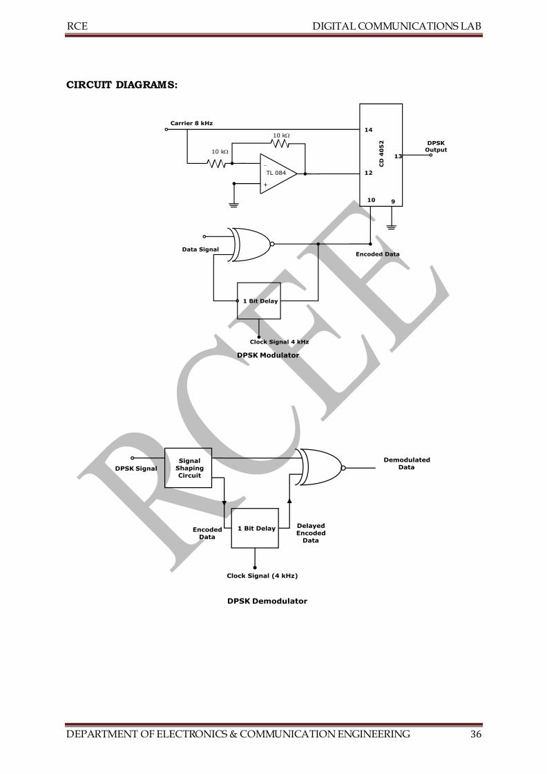
DPSK DEMODULATOR: Fig shows the DPSK modulator. This consists of PSK
modulator and differential encoder. PSK Modulator: IC CD 4052 is a 4 channel
analog multiplexer and is used as an active component in this circuit. One of the
control signals of 4052 is grounded so that 4052 will act as a two channel
multiplexer and other control is being connected to the binary signal i.e., encoded
data. Un shifted carrier signal is connected directly to CH1 and carrier shifted by
1800is connected to CH2. Phase shift network is a unity gain inverting amplifier
using Op-Amp (TL084).
When control signal is at high voltage, output of the 4052 is connected to
CH1 and un-shifted (or 0 phase) carrier is passed on to output. Similarly when
control signal is at zero voltage output of 4052 is connected to CH2 and carrier
shifted by 1800 is passed on to output.
Differential encoder: This consists of 1 bit delay circuit and an X-NOR Gate. 1 bit
delay circuit is formed by a D-Latch. Data signal i.e., signal to be transmitted is
connected to one of the input of the X-NOR gate and other one being connected to
out of the delay circuit. Output of the X-NOR gate and is connected to control
input of the multiplexer (IC 4052) and as well as to input of the D-Latch. Output of
the X-NOR gate is 1 when both the inputs are same and it is 0 when both the
inputs are different.
RCE DIGITAL COMMUNICATIONS LAB
DEPARTMENT OF ELECTRONICS & COMMUNICATION ENGINEERING 36
CIRCUIT DIAGRAMS:
RCE DIGITAL COMMUNICATIONS LAB
DEPARTMENT OF ELECTRONICS & COMMUNICATION ENGINEERING 37
DPSK DEMODULATOR: Second fig shows the DPSK Demodulator. This consists
of 1 bit delay circuit, X-NOR Gate and a signal shaping circuit. Signal shaping
circuit consists of an Op-amp based zero crossing detector followed by a D-latch.
Receiver DPSK signal is converted to square wave with the help of zero crossing
and this square wave will pass through the D-Latch. So output of the D-latch is an
encoded data. This encoded data is applied to 1 bit delay circuit as well as to one
of the inputs of X-NOR gate. And output of the delay circuit is connected to
another input of the X-NOR gate. Output of the X-NOR gate is 1 when both the
inputs are same and it is 0 when both the inputs are different.
PROCEDURE:
MODULATION:
1. Connect carrier signal to carrier input of the PSK Modulator.
2. Connect data signal from data input of the X-NOR gate.
3. Keep CRO in dual mode.
4. Connect CH1 input of the CRO to data signal and CH2 input to the encoded
data (which is nothing but the output of the X-NOR gate)
5. Observe the encoded data with respect to data input. The encoded data will
be in a given sequence.
Actual data signal : 10101101001010110100
Encoded data signal : 01100011011001110010
6. Now connect CH2 input of the CRO to the DPSK output and CH1 input to
the encoded data. Observe the input and output waveforms and plot the
same.
7. Compare the plotted waveforms with the given waveforms in fig.
Note: Observe and plot the waveforms after perfect triggering. Better to keep
the encoded data more than 4 cycles for perfect triggering.
DEMODULATION:
1. Connect DPSK signal to the input of the signal shaping circuit from DPSK
transmitter with the help of coaxial cable (supplied with trainer).
2. Connect clock from the transmitter (i.e. DPSK Modulator) to clock input of
the 1 bit delay circuit using coaxial cable.
3. Keep CRO in dual mode. Connect CH1 input to the encoded data (at
modulator) and CH2 input to the encoded data (at demodulator).
RCE DIGITAL COMMUNICATIONS LAB
DEPARTMENT OF ELECTRONICS & COMMUNICATION ENGINEERING 38
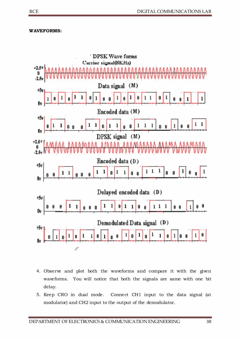
WAVEFORMS:
4. Observe and plot both the waveforms and compare it with the given
waveforms. You will notice that both the signals are same with one bit
delay.
5. Keep CRO in dual mode. Connect CH1 input to the data signal (at
modulator) and CH2 input to the output of the demodulator.
RCE DIGITAL COMMUNICATIONS LAB
DEPARTMENT OF ELECTRONICS & COMMUNICATION ENGINEERING 39
6. Observe and plot both the waveforms and compare it with the given
waveforms. You will notice that both the signals are same with one bit delay.
7. Disconnect clock from transmitter and connect to local oscillator clock (i.e.,
clock generator output from De Modulator) with remaining setup as it is.
Observe demodulator output and compare it with the previous output. This
signal is little bit distorted. This is because lack of synchronization between
clock at modulator and clock at demodulator. You can get further perfection
in output waveform by adjusting the locally generated clock frequency by
varying potentiometer.
RESULT:
VIVA QUESTIONS:
1. Define DPSK.
2. What is the difference between PSK and DPSK?
3. What are the operations of DPSK?
4. What are the applications of DPSK?
5. Write the truth table for XNOR gate?
6. What is meant by encoded data?
7. What is the error probability for DPSK?

RCE DIGITAL COMMUNICATIONS LAB
DEPARTMENT OF ELECTRONICS & COMMUNICATION ENGINEERING 40
8. COMPANDING Introduction
Companding is a compressing and expanding technique used in digital
communication systems. With this technique we can improve noise performance at low level
signals and improve the dynamic range of the signal that can be handled by the channel.
Aim of the experiment The student notes down the dynamic range of the signal and S/Q without companding and
with companding .
The student observes the improvement in dynamic range and the noise performance with
companding and records the same.
Specification
The kit is implemented with 16 bit micro controller giving lot of flexibility in experimenting
Full signal chain implementation i.e 16 bit A/D , Compress coder, Decoder, 16 bit D/A.
Facility to observe the signal chain without companding and with companding and noting
the difference
Facility to feed precise dc voltage using up/down keys
Facility to feed a fixed frequency ac input
Facility to observe the linear code and compressed code on LEDS
Bipolar input and bipolar output
Theory While coding the signal we give higher resolution at low levels and and lower resolution at
higher levels. This makes the signal compresed in the code domain.
By applying the reverse mapping at the decoding end we get back the original signal.
By allocating more bits at lower signal levels we can reduce the quantization noise ( the
noise created by the LSB),
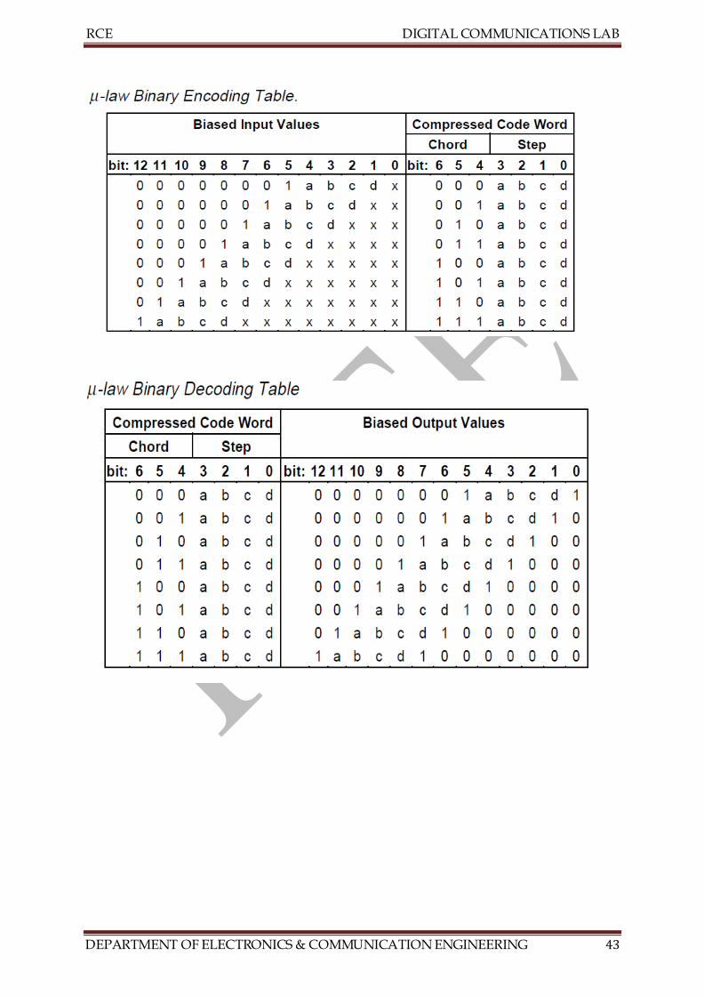
The µ-law and A-law algorithms encode 14-bit and 13-bit signed linear PCM samples
(respectively) to logarithmic 8-bit samples. Thus, the G.711 encoder will create a 64 kbit/s
bitstream for a signal sampled at 8 kHz.[1]
G.711 μ-law tends to give more resolution to higher range signals while G.711 A-law
provides more quantization levels at lower signal levels.
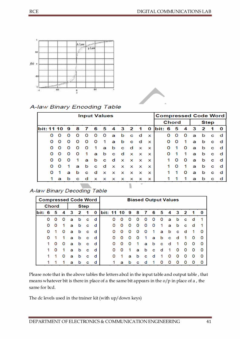
The companding curve for A law and u law, note that for low level input ( x axis) variation
in the chalnnel code high ( f(x), where as at higher levels variation in is smaller.
RCE DIGITAL COMMUNICATIONS LAB
DEPARTMENT OF ELECTRONICS & COMMUNICATION ENGINEERING 41
Please note that in the above tables the letters abcd in the input table and output table , that
means whatever bit is there in place of a the same bit appears in the o/p in place of a , the
same for bcd.
The dc levels used in the trainer kit (with up/down keys)
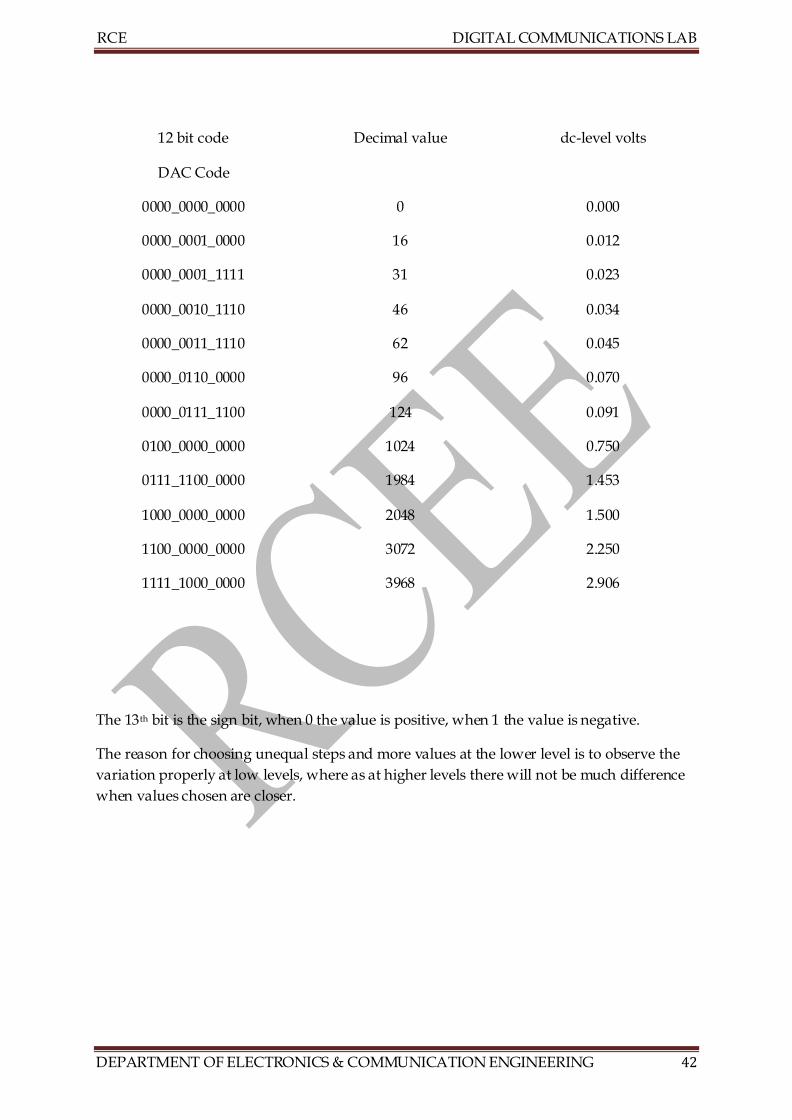
RCE DIGITAL COMMUNICATIONS LAB
DEPARTMENT OF ELECTRONICS & COMMUNICATION ENGINEERING 42
12 bit code
DAC Code
Decimal value dc-level volts
0000_0000_0000 0 0.000
0000_0001_0000 16 0.012
0000_0001_1111 31 0.023
0000_0010_1110 46 0.034
0000_0011_1110 62 0.045
0000_0110_0000 96 0.070
0000_0111_1100 124 0.091
0100_0000_0000 1024 0.750
0111_1100_0000 1984 1.453
1000_0000_0000 2048 1.500
1100_0000_0000 3072 2.250
1111_1000_0000 3968 2.906
The 13th bit is the sign bit, when 0 the value is positive, when 1 the value is negative.
The reason for choosing unequal steps and more values at the lower level is to observe the
variation properly at low levels, where as at higher levels there will not be much difference
when values chosen are closer.
RCE DIGITAL COMMUNICATIONS LAB
DEPARTMENT OF ELECTRONICS & COMMUNICATION ENGINEERING 43

RCE DIGITAL COMMUNICATIONS LAB
DEPARTMENT OF ELECTRONICS & COMMUNICATION ENGINEERING 44
The kit signal chain has the following blocks
Signal Generator:
The kit generates -3 to +3 DC Voltage at the input by using the UP/DOWN keys in DC
mode.
The kit also generates a fixed ac waveform when the switch is in AC Mode.
A/D Convertor:
This is a 16 bit A/D convertor, for commanding we need the following sizes of A/D , for
linear 8 bit, for A law 13 bit, for u law 14 bit. the most significant bit is used for signal sign ,
bit is 1 means negative from the 16 bit convertor we get the sign bit and 15 bit magnitude.
for linear case we take the most significant 7 bits from the magnitude and the sign bit to sign
bit.
for A law we take sign bit sign bit, most significant 12 bit as magnitude of the input.
for u law we are showing only the magnitude bits on LEDS. the sign bit is not shown.
The compressor:
The compressor converts the 12 bit magnitude to coded 7 bits ( A law).
these 7 bits along with the sign bit go out on the channel of communication.
The Expander:
The expander converts the 7 coded magnitude back to the original 12 bit magnitude ( A
law).
D/A:
The D/A is 16 bit implementation, the expander output sign bit gets loaded as sign bit , the
magnitude 12 bits get loaded to the most significant 12 bits of the D/A.
Procedure:
Use the Fluke87V (4 ½ digit) multi meter for observing the dc levels or any other suitable
dc volt meter with 0.05% accuracy, which can distinguish 1mv, since the we need to observe
the errors in dc level in the range of 0.001 volts/ i.e., 1 mv . if you are using 31/2 digit DMM
it should have 0-200 mv range to measure 000.0 to 199.9 mv
1. First observe the communication blocks in the signal chain 2. Apply a given dc voltage at the input by using the up/down keys, measure this
with multi meter. after reset it starts with 0 volts. 3. Note down the codes and the voltages as per the table given below. 4. Do this for both the linear mode and companded mod ( A Law). 5. Observe that higher Quantisation error Q/S in the case of linear mode compared
to the companded mode.
RCE DIGITAL COMMUNICATIONS LAB
DEPARTMENT OF ELECTRONICS & COMMUNICATION ENGINEERING 45
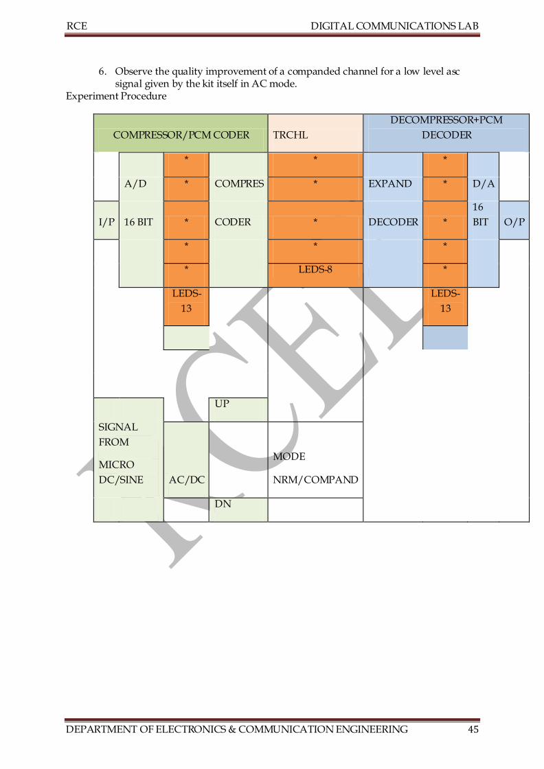
6. Observe the quality improvement of a companded channel for a low level asc signal given by the kit itself in AC mode.
Experiment Procedure
COMPRESSOR/PCM CODER TRCHL
DECOMPRESSOR+PCM
DECODER
* * *
A/D * COMPRES * EXPAND * D/A
I/P 16 BIT * CODER * DECODER *
16
BIT O/P
* * *
* LEDS-8 *
LEDS-
13
LEDS-
13
UP
SIGNAL
FROM
MICRO
DC/SINE AC/DC
MODE
NRM/COMPAND
DN
RCE DIGITAL COMMUNICATIONS LAB
DEPARTMENT OF ELECTRONICS & COMMUNICATION ENGINEERING 46
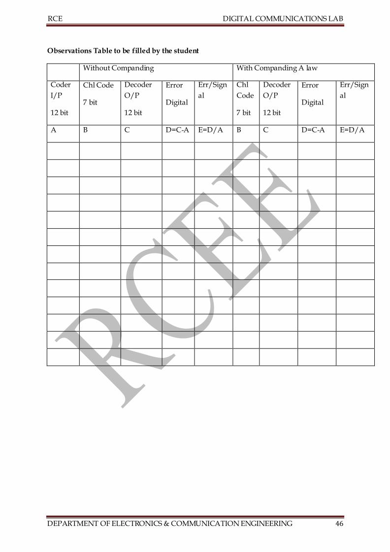
Observations Table to be filled by the student
Without Companding With Companding A law
Coder
I/P
12 bit
Chl Code
7 bit
Decoder
O/P
12 bit
Error
Digital
Err/Sign
al
Chl
Code
7 bit
Decoder
O/P
12 bit
Error
Digital
Err/Sign
al
A B C D=C-A E=D/A B C D=C-A E=D/A
RCE DIGITAL COMMUNICATIONS LAB
DEPARTMENT OF ELECTRONICS & COMMUNICATION ENGINEERING 47
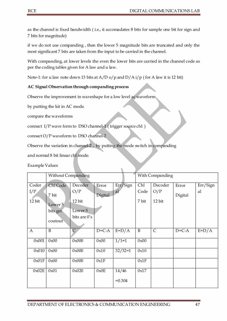
as the channel is fixed bandwidth ( i.e., it accomadates 8 bits for sample one bit for sign and
7 bits for magnitude)
if we do not use companding , then the lower 5 magnitude bits are truncated and only the
most significant 7 bits are taken from the input to be carried in the channel.
With companding, at lower levels the even the lower bits are carried in the channel code as
per the coding tables given for A law and u law.
Note-1: for u law note down 13 bits at A/D o/p and D/A i/p ( for A law it is 12 bit)
AC Signal Observation through companding process
Observe the improvement in waveshape for a low level ac waveform
by putting the kit in AC mode.
compare the waveforms
connect I/P wave form to DSO channel-1 ( trigger source ch1 )
connect O/P waveform to DSO channel-2
Observe the variation in channel-2 , by putting the mode switch in companding
and normal 8 bit linear chl mode.
Example Values
Without Companding With Companding
Coder
I/P
12 bit
Chl Code
7 bit
Lower 5
bits get
coutout
Decoder
O/P
12 bit
Lower 5
bits are 0’s
Error
Digital
Err/Sign
al
Chl
Code
7 bit
Decoder
O/P
12 bit
Error
Digital
Err/Sign
al
A B C D=C-A E=D/A B C D=C-A E=D/A
0x001 0x00 0x000 0x00 1/1=1 0x00
0x010 0x00 0x000 0x10 32/32=1 0x10
0x01F 0x00 0x000 0x1F 0x1F
0x02E 0x01 0x020 0x0E 14/46
=0.304
0x17
RCE DIGITAL COMMUNICATIONS LAB
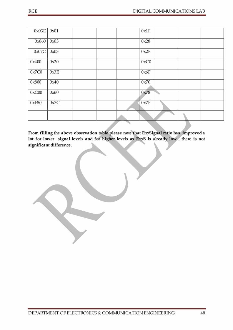
DEPARTMENT OF ELECTRONICS & COMMUNICATION ENGINEERING 48
0x03E 0x01 0x1F
0x060 0x03 0x28
0x07C 0x03 0x2F
0x400 0x20 0xC0
0x7C0 0x3E 0x6F
0x800 0x40 0x70
0xC00 0x60 0x78
0xF80 0x7C 0x7F
From filling the above observation table please note that Err/Signal ratio has improved a
lot for lower signal levels and for higher levels as Err/S is already low , there is not
significant difference.
RCE DIGITAL COMMUNICATIONS LAB
DEPARTMENT OF ELECTRONICS & COMMUNICATION ENGINEERING 49
9. SOURCE ENCODER AND DECODER Introduction Source Coding is a technique of compressing the source information size based on the
probability of occurrence of each information symbol.
Decoding is the reverse process to get back the full source information.
In every day we employ this in transferring big files, particularly image/voice files by
zipping them and transferring to the destination and unzipping at the destination.
Example: Huffman coding
Aim of the experiment To select an information having in-equal probability of occurrence of each symbol or having
redundancy in the information and applying a source code using one of the techniques i.e
Huffman coding, observing the size of the coded information, sending the minimized packet
, decoding at the receiving end getting back the full information sent.
Theory When we have to transmit a set of symbols over a communication channels, normally
choose no of bits to accommodate all the symbols for example 8 symbols can be coded using
3 bits, because 3 bits give us 2^3=8 combinations. With this type of normal binary
representation we can transfer any combination of symbols in any order. However if our
information to be transmitted has a set of symbols but the occurrence of symbols with
different frequencies we can employ a coding technique whereby we choose less no of bits
for the frequently occurring symbol and more bits for the less occurring symbol this way we
can represent our information which is a sequence of symbols with less no.of bits i.e.
reduced size.
In everyday language, we call this zipping.
Huffman coding is based on the frequency of occurrence of a data item (pixel in images).
The principle is to use a lower number of bits to encode the data that occurs more
frequently. Codes are stored in a Code Book which may be constructed for each image or a
set of images. In all cases the code book plus encoded data must be transmitted to enable
decoding.
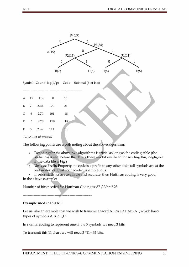
The Huffman algorithm is now briefly summarized:
A bottom-up approach 1. Initialization: Put all nodes in an OPEN list, keep it sorted at all times (e.g., ABCDE). 2. Repeat until the OPEN list has only one node left:
(a) From OPEN pick two nodes having the lowest frequencies/probabilities, create a parent node of them.
(b) Assign the sum of the children's frequencies/probabilities to the parent node and insert it into OPEN.
(c) Assign code 0, 1 to the two branches of the tree, and delete the children from OPEN.
RCE DIGITAL COMMUNICATIONS LAB
DEPARTMENT OF ELECTRONICS & COMMUNICATION ENGINEERING 50
Symbol Count log(1/p) Code Subtotal (# of bits)
------ ----- -------- --------- --------------------
A 15 1.38 0 15
B 7 2.48 100 21
C 6 2.70 101 18
D 6 2.70 110 18
E 5 2.96 111 15
TOTAL (# of bits): 87
The following points are worth noting about the above algorithm:
Decoding for the above two algorithms is trivial as long as the coding table (the statistics) is sent before the data. (There is a bit overhead for sending this, negligible if the data file is big.)
Unique Prefix Property: no code is a prefix to any other code (all symbols are at the
leaf nodes) -> great for decoder, unambiguous. If prior statistics are available and accurate, then Huffman coding is very good.
In the above example:
Number of bits needed for Huffman Coding is: 87 / 39 = 2.23
-----------------------------------------------------------
Example used in this kit
Let us take an example that we wish to transmit a word ABRAKADABRA , which has 5
types of symbols A,B,R,C,D
In normal coding to represent one of the 5 symbols we need 3 bits.
To transmit this 11 chars we will need 3 *11= 33 bits.
RCE DIGITAL COMMUNICATIONS LAB
DEPARTMENT OF ELECTRONICS & COMMUNICATION ENGINEERING 51
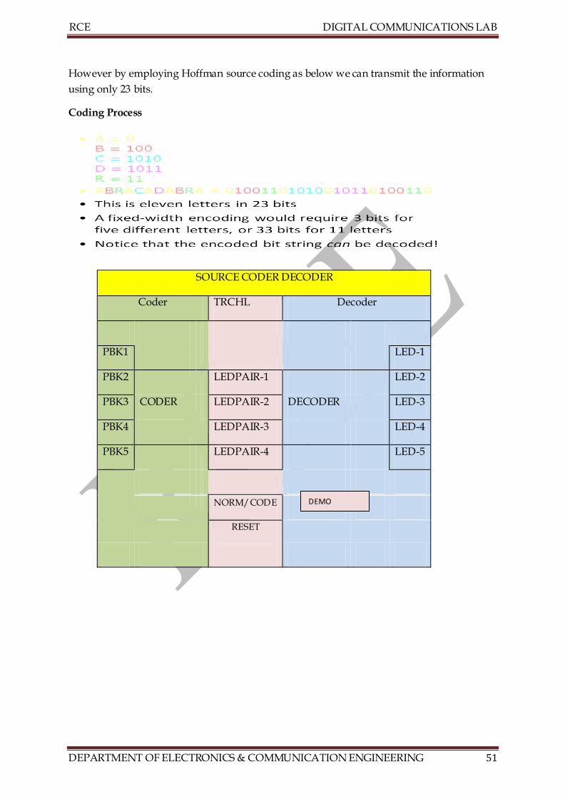
However by employing Hoffman source coding as below we can transmit the information
using only 23 bits.
Coding Process
SOURCE CODER DECODER
Coder TRCHL Decoder
PBK1 LED-1
PBK2 LEDPAIR-1 LED-2
PBK3 CODER LEDPAIR-2 DECODER LED-3
PBK4 LEDPAIR-3 LED-4
PBK5 LEDPAIR-4 LED-5
NORM/CODE
RESET
DEMO
RCE DIGITAL COMMUNICATIONS LAB
DEPARTMENT OF ELECTRONICS & COMMUNICATION ENGINEERING 52
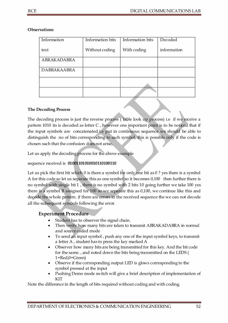
Observations
Information
text
Information bits
Without coding
Information bits
With coding
Decoded
information
ABRAKADABRA
DABRAKAABRA
The Decoding Process
The decoding process is just the reverse process ( table look up process) i.e if we receive a
pattern 1010 its is decoded as letter C , however one important point is to be noticed that if
the input symbols are concatenated i.e put in continuous sequence we should be able to
distinguish the no of bits corresponding to each symbol, this is possible only if the code is
chosen such that the confusion does not arise,
Let us apply the decoding process for the above example
sequence received is 01001101010010110100110
Let us pick the first bit which 0 is there a symbol for only one bit as 0 ? yes there is a symbol
A for this code so let us separate this as one symbol so it becomes 0,100 then further there is
no symbol with single bit 1 , there is no symbol with 2 bits 10 going further we take 100 yes
there is a symbol B assigned for 100 so we separate this as 0,100, we continue like this and
decode the whole pattern. if there are errors in the received sequence the we can not decode
all the subsequent symbols following the error.
Experiment Procedure
Student has to observer the signal chain. Then verify how many bits are taken to transmit ABRAKADABRA in normal
and source coded mode
To send an input symbol , push any one of the input symbol keys, to transmit a letter A , student has to press the key marked A
Observer how many bits are being transmitted for this key. And the bit code
for the same. , and noted down the bits being transmitted on the LEDS ( 1=Red,0=Green)
Observe if the corresponding output LED is glows corresponding to the
symbol pressed at the input Pushing Demo mode switch will give a brief description of implementation of
KIT Note the difference in the length of bits required without coding and with coding.
RCE DIGITAL COMMUNICATIONS LAB
DEPARTMENT OF ELECTRONICS & COMMUNICATION ENGINEERING 53
10. LINEAR BLOCK CODES
HAMMING (7,4) CODE IS USED IN THIS EXPERIMENT, THIS IS A SYSTEMATIC CODE.
This topic comes under channel coding techniques which are employed for the purpose of
detecting and correcting errors occurring in the communication channel. When information
is represented in blocks of k bits we can add few extra bits increasing the block size to n bits
and employ block coding techniques to detect and correct errors in the reception.
Examples: Hamming Code (n, k), Checksum, CRC8, CRC16
Aim of the experiment To observe that the errors received through a noisy channel can be removed / minimized by
employing the error detection and correction code.
Specification
The kit is implemented with 16 bit micro controller giving lot of flexibility in experimenting
Facility to inject a custom bit stream as an input message
Verification of the injected bit stream on LEDS
Verification of the code word on LEDS
Facility to add multiple errors
Facility to observe the decoded output
Facility to observe the status of decoding i.e. error detected and error corrected status on LEDS
Option keys to normal mode or code mode
Easy verification of where error is injected and what is the corresponding output.
Demo mode support
Theory We can add a few extra bits to the information bits i.e. provide some redundancy and detect
/ correct the errors from the received data.
More redundancy we provide more correction we can have. By using hamming coding
technique with given no. of extra bits we can extract maximum advantage of detection and
correction.
Hamming code (n,k) places symbols represented by n bits having k information bits
at a maximum distance from each other allowing us to detect more errors and correct more
errors.
RCE DIGITAL COMMUNICATIONS LAB
DEPARTMENT OF ELECTRONICS & COMMUNICATION ENGINEERING 54
The decoder if it finds the errors which cannot be corrected, it shows the O/P but
indicates that the same with error LED at the output. Normally if in applications using
command and control the decoded O/P having errors is not used it is discarded.
Hamming code(7,4) is used in this kit.
mbols used
X= Input data row vector 1*4
G= Generator Matrix 4*7
P= Parity SubMatrix 4*3
H= Parity Check Matrix 3*7
G= [P:I] a concatenation of P and I
if Y is the received data then the Syndrome S should be all zeros/null vector if there are no
errors , if there are errors in the received data S will not be null , then we check which
column in HT has same values as S then that co
S=YHT
where Y is the channel code with errors
and H is the hamming parity matrix
/* code matrix 2nd, 3rd, and 4th MSB define parity bits */
The kit uses generator matrix g[4*4]=P:I=
0111000
1010100
1100010
1110001
where P[4*3]=
011
101
110
111
where I[4*4]=
1000
0100
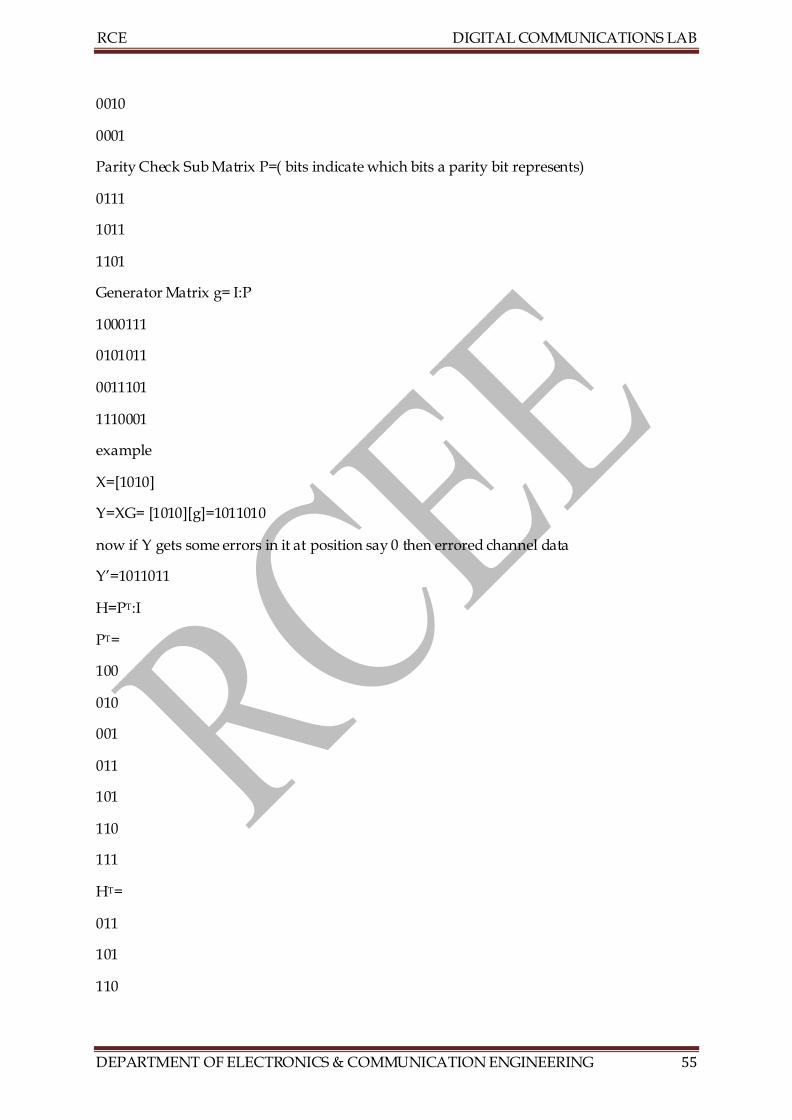
RCE DIGITAL COMMUNICATIONS LAB
DEPARTMENT OF ELECTRONICS & COMMUNICATION ENGINEERING 55
0010
0001
Parity Check Sub Matrix P=( bits indicate which bits a parity bit represents)
0111
1011
1101
Generator Matrix g= I:P
1000111
0101011
0011101
1110001
example
X=[1010]
Y=XG= [1010][g]=1011010
now if Y gets some errors in it at position say 0 then errored channel data
Y’=1011011
H=PT:I
PT=
100
010
001
011
101
110
111
HT=
011
101
110
RCE DIGITAL COMMUNICATIONS LAB
DEPARTMENT OF ELECTRONICS & COMMUNICATION ENGINEERING 56
111
100
010
001
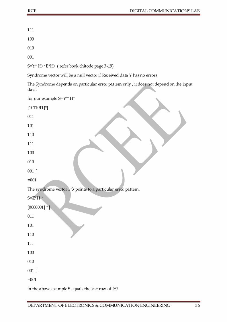
S=Y* HT = E*HT ( refer book chitode page 3-19)
Syndrome vector will be a null vector if Received data Y has no errors
The Syndrome depends on particular error pattern only , it does not depend on the input
data.
for our example S=Y’* HT
[1011011]*[
011
101
110
111
100
010
001 ]
=001
The syndrome vector 1*3 points to a particular error pattern.
S=E*HT=
[0000001] * [
011
101
110
111
100
010
001 ]
=001
in the above example S equals the last row of HT
RCE DIGITAL COMMUNICATIONS LAB
DEPARTMENT OF ELECTRONICS & COMMUNICATION ENGINEERING 57
so the last row matching syndrome indicates that the last bit in Y is in error.
like wise if S matches the nth row of HT from one ed,we have to correct nth bit of Y from
the same end.
for more than one error this correction logic does not work , only we can say if syndrome
exist then there are errors in the data.
RCE DIGITAL COMMUNICATIONS LAB
DEPARTMENT OF ELECTRONICS & COMMUNICATION ENGINEERING 58
------------------------------------------------------------------------------
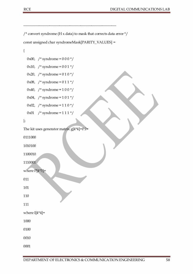
/* convert syndrome (H x data) to mask that corrects data error */
const unsigned char syndromeMask[PARITY_VALUES] =
{
0x00, /* syndrome = 0 0 0 */
0x10, /* syndrome = 0 0 1 */
0x20, /* syndrome = 0 1 0 */
0x08, /* syndrome = 0 1 1 */
0x40, /* syndrome = 1 0 0 */
0x04, /* syndrome = 1 0 1 */
0x02, /* syndrome = 1 1 0 */
0x01 /* syndrome = 1 1 1 */
};
The kit uses generator matrix g[4*4]=P:I=
0111000
1010100
1100010
1110001
where P[4*3]=
011
101
110
111
where I[4*4]=
1000
0100
0010
0001
RCE DIGITAL COMMUNICATIONS LAB
DEPARTMENT OF ELECTRONICS & COMMUNICATION ENGINEERING 59
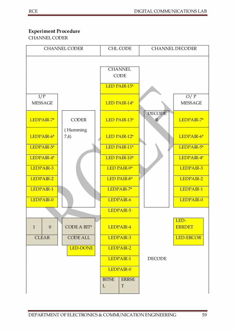
Experiment Procedure
CHANNEL CODER
CHANNEL CODER CHL CODE CHANNEL DECODER
CHANNEL
CODE
LED PAIR-15*
I/P
MESSAGE
LED PAIR-14*
O/ P
MESSAGE
LEDPAIR-7*
CODER
LED PAIR-13*
DECODE
R
LEDPAIR-7*
LEDPAIR-6*
( Hamming
7,4)
LED PAIR-12*
LEDPAIR-6*
LEDPAIR-5*
LED PAIR-11*
LEDPAIR-5*
LEDPAIR-4*
LED PAIR-10*
LEDPAIR-4*
LEDPAIR-3
LED PAIR-9*
LEDPAIR-3
LEDPAIR-2
LED PAIR-8*
LEDPAIR-2
LEDPAIR-1
LEDPAIR-7*
LEDPAIR-1
LEDPAIR-0
LEDPAIR-6
LEDPAIR-0
LEDPAIR-5
1 0
CODE A BIT*
LEDPAIR-4
LED-
ERRDET
CLEAR
CODE ALL
LEDPAIR-3
LED-ERCOR
LED-DONE
LEDPAIR-2
LEDPAIR-1
DECODE
LEDPAIR-0
BITSE
L
ERRSE
T
RCE DIGITAL COMMUNICATIONS LAB
DEPARTMENT OF ELECTRONICS & COMMUNICATION ENGINEERING 60
RESETKIT
NORM
DEMO
/COD
E
Procedure:
Observe the signal chain , i.e. the input stage, coding stage, transmission stage and the decode stage
Put the mode selection switch in NORMAL mode and see the process and observe output
Student selects input message that is to be coded, by shifting the bits 0/1 by means of pressing the keys 0, 1, CLEAR.
Student codes this input message by pushing the key ‘CODE A BIT’ or by pushing ‘CODEALL’.
Now the message is coded and displayed in the transmission path. Student can now introduce an error in the transmission channel by means of pressing the keys BITSEL and ERRSET. On every push of the BITSEL one bit is selected in the channel
code, the selected bit will be completely in OFF mode at this stage, if the student presses ERRSET key, the OFF mode bit will be inverted to make it as an error.
Now the student pushes the DECODE key, the channel code is decoded and displayed as the Output message. If an error is detected in the channel code
ERRDETECTED LED glows, if an error is corrected from channel code then the ERRCORRECTED LED glows in the decoder Output stage.
Now put mode selection in CODE mode and repeat the process and observe the output changes.
Observe how the error detection and correction in code mode and hence the
implementation of Linear Block encoder and decoder. Pushing Demo mode switch will give a brief description of implementation of KIT
In this experiment hamming code (7.4) is employed. the input data is limited to 4 bits, once
it is coded the input data is placed in channel data positions 1..4(d0-d3), parity bits are place
in positions 5,6,7 (d4-d6) this is a systematic code. To set errors in a different position for the
same input data, press code-all key once, then it will be recoded and shown on channel
data and o/p gets cleared waiting for decode key once again.
RCE DIGITAL COMMUNICATIONS LAB
DEPARTMENT OF ELECTRONICS & COMMUNICATION ENGINEERING 61
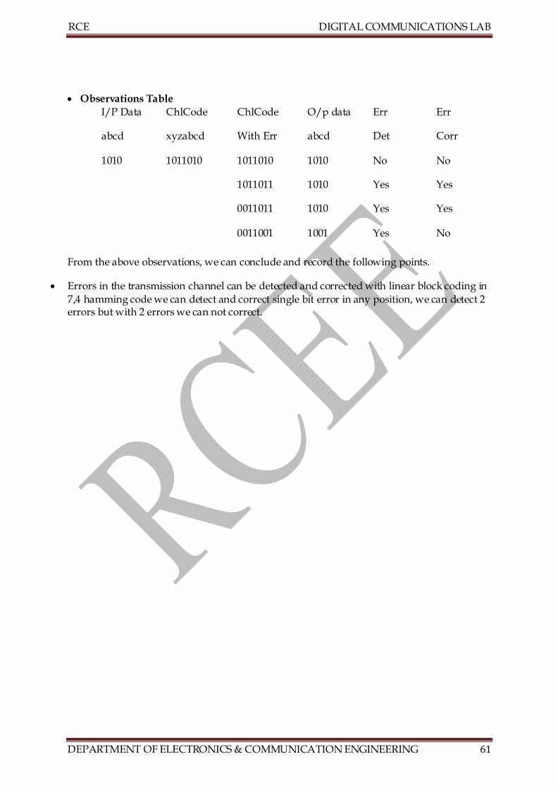
Observations Table
I/P Data
abcd
ChlCode
xyzabcd
ChlCode
With Err
O/p data
abcd
Err
Det
Err
Corr
1010 1011010 1011010 1010 No No
1011011 1010 Yes Yes
0011011 1010 Yes Yes
0011001 1001 Yes No
From the above observations, we can conclude and record the following points.
Errors in the transmission channel can be detected and corrected with linear block coding in
7,4 hamming code we can detect and correct single bit error in any position, we can detect 2 errors but with 2 errors we can not correct.
RCE DIGITAL COMMUNICATIONS LAB
DEPARTMENT OF ELECTRONICS & COMMUNICATION ENGINEERING 62
11. BINARY CYCLIC CODE ENCODER AND DECODER In coding theory cyclic codes are the sub-class of linear block error correcting codes that
have convenient algebraic structures for efficient error detection and correction.
Aim of the experiment To observe that the errors received through a noisy channel can be removed / minimized by
employing the error detection and correction code, by using an algebraic structure.
Specification
The kit is implemented with 16 bit micro controller giving lot of flexibility in experimenting
Facility to inject a custom bit stream as an input message
Verification of the injected bit stream on LEDS
Verification of the code word on LEDS
Facility to add multiple errors
Facility to observe the decoded output
Facility to observe the status of decoding i.e. error detected and error corrected status on
LEDS
Option keys to select one of normal mode or code mode
Easy verification of where error is injected and what is the corresponding output.
Theory A linear code is called cyclic code if every cycle shift of code vector produces some other
code vector i.e. the cycle shift to the data in an array should also represent the data in the
same array.
Example: arr{(0000),(0101),(1010),(1111)}
There are two cyclic codes encoding techniques:
Nonsystematic: Encoded data is obtained by performing M(p) * G(p). Systematic : Coded data(C2C1C0) is obtained by performing pq * M(p)/G(p) and
resultant Encoded data will be in form of M3M2M1M0C2C1C0 Here M(p) is input Message/Data of p
G(p) is constant algebraic expression of p
q is constraint length i.e. Systamatic (7,4) gives q = n-k
n is channel length and
k is data length
RCE DIGITAL COMMUNICATIONS LAB
DEPARTMENT OF ELECTRONICS & COMMUNICATION ENGINEERING 63
Experiment Procedure Let us consider an example for implementation of the experiment
Q) Design the encoder for the Systematic (7,4) cyclic code generated by a polynomial G(p)
= p3 + p + 1 and decode the data transferred by syndrome decoding procedure for
knowing input.
The implementation of cyclic encoding and decoding kit is based on the same example as
per Reference 1. The encoded data output will be M3M2M1M0C2C1C0 which is can be
obtained from Systematic coding procedure and the decoding the data will be done by
syndrome decoding procedure to re generate input and correct the data received from any
noisy channel.
Procedure:
Observe the signal chain , i.e. the input stage, coding stage, transmission stage and the decode stage
Put the mode selection switch in NORMAL mode and see the process and observe
output Student selects input message that is to be coded, by shifting the bits 0/1 by means
of pressing the keys 0, 1, CLEAR. Student codes this input message by pushing the key ‘CODE A BIT’ or by pushing
‘CODEALL’.
Now the message is coded and displayed in the transmission path. Student can now introduce an error in the transmission channel by means of pressing the keys BITSEL and ERRSET. On every push of the BITSEL one
RCE DIGITAL COMMUNICATIONS LAB
DEPARTMENT OF ELECTRONICS & COMMUNICATION ENGINEERING 64
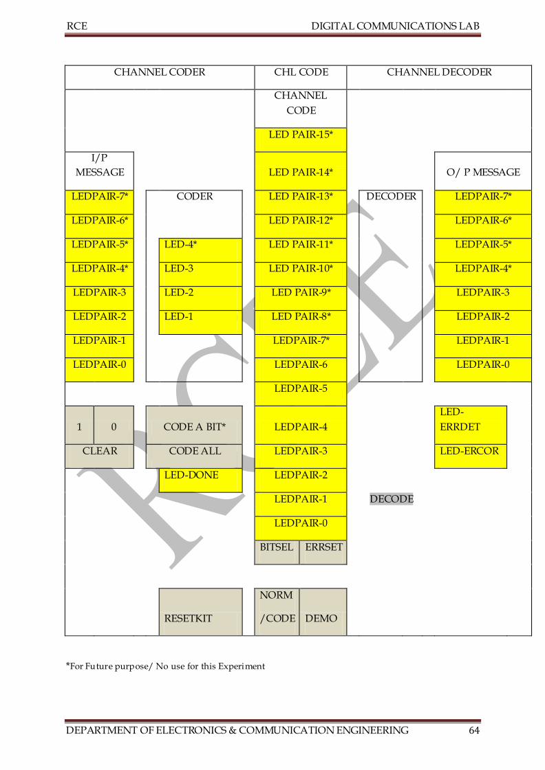
CHANNEL CODER CHL CODE CHANNEL DECODER
CHANNEL
CODE
LED PAIR-15*
I/P
MESSAGE
LED PAIR-14*
O/ P MESSAGE
LEDPAIR-7*
CODER
LED PAIR-13*
DECODER
LEDPAIR-7*
LEDPAIR-6*
LED PAIR-12*
LEDPAIR-6*
LEDPAIR-5*
LED-4*
LED PAIR-11*
LEDPAIR-5*
LEDPAIR-4*
LED-3
LED PAIR-10*
LEDPAIR-4*
LEDPAIR-3
LED-2
LED PAIR-9*
LEDPAIR-3
LEDPAIR-2
LED-1
LED PAIR-8*
LEDPAIR-2
LEDPAIR-1
LEDPAIR-7*
LEDPAIR-1
LEDPAIR-0
LEDPAIR-6
LEDPAIR-0
LEDPAIR-5
1 0
CODE A BIT*
LEDPAIR-4
LED-
ERRDET
CLEAR
CODE ALL
LEDPAIR-3
LED-ERCOR
LED-DONE
LEDPAIR-2
LEDPAIR-1
DECODE
LEDPAIR-0
BITSEL ERRSET
RESETKIT
NORM
/CODE DEMO
*For Future purpose/ No use for this Experiment
RCE DIGITAL COMMUNICATIONS LAB
DEPARTMENT OF ELECTRONICS & COMMUNICATION ENGINEERING 65
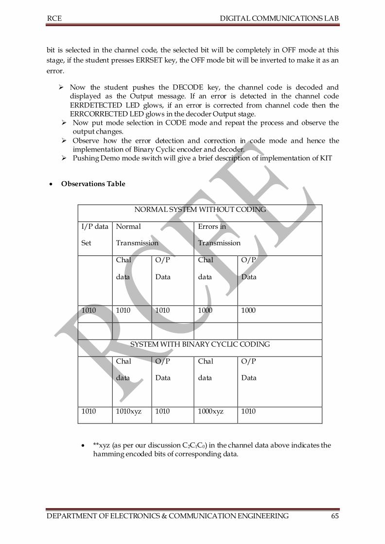
bit is selected in the channel code, the selected bit will be completely in OFF mode at this
stage, if the student presses ERRSET key, the OFF mode bit will be inverted to make it as an
error.
Now the student pushes the DECODE key, the channel code is decoded and displayed as the Output message. If an error is detected in the channel code
ERRDETECTED LED glows, if an error is corrected from channel code then the ERRCORRECTED LED glows in the decoder Output stage.
Now put mode selection in CODE mode and repeat the process and observe the output changes.
Observe how the error detection and correction in code mode and hence the implementation of Binary Cyclic encoder and decoder.
Pushing Demo mode switch will give a brief description of implementation of KIT
Observations Table
NORMAL SYSTEM WITHOUT CODING
I/P data
Set
Normal
Transmission
Errors in
Transmission
Chal
data
O/P
Data
Chal
data
O/P
Data
1010 1010 1010 1000 1000
SYSTEM WITH BINARY CYCLIC CODING
Chal
data
O/P
Data
Chal
data
O/P
Data
1010 1010xyz 1010 1000xyz 1010
**xyz (as per our discussion C2C1C0) in the channel data above indicates the hamming encoded bits of corresponding data.
RCE DIGITAL COMMUNICATIONS LAB
DEPARTMENT OF ELECTRONICS & COMMUNICATION ENGINEERING 66
12. CONVOLUTION CODE ENCODER AND DECODER
This topic comes under channel coding techniques which are employed for the purpose of
detecting and correcting errors, occurring in the communication channel.
Convolution coding is a special case of error-control coding.
Unlike a block coder, a convolution coder is a memory based device. Even though a
convolution coder accepts a fixed number of message symbols and produces a
fixed number of code symbols, its computations depend not only on the current set of input
symbols but on some of the previous input symbols.
Normally represented as (n, m, k) code
Where,
n= no of output bits
m= no of message bits
k= no of constraint bits/ memory bits
Terms:
Trellis code, Viterbi decoding algorithm
Aim of the experiment Employ one of the convolution codes and observe its error correcting performance
and decode-ability.
Specification
The kit is implemented with 16 bit micro controller giving lot of flexibility in experimenting
Facility to inject a custom bit stream as an input message
Verification of the injected bit stream on LEDS
Verification of the code word on LEDS
Facility to add multiple errors
Facility to observe the decoded output
Facility to observe the status of decoding i.e. error detected and error corrected status on
LEDS
Option keys to normal mode or code mode
Easy verification of where error is injected and what is the corresponding output.
RCE DIGITAL COMMUNICATIONS LAB
DEPARTMENT OF ELECTRONICS & COMMUNICATION ENGINEERING 67
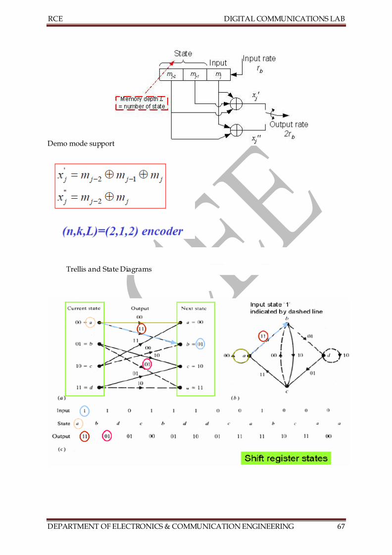
Demo mode support
Trellis and State Diagrams
RCE DIGITAL COMMUNICATIONS LAB
DEPARTMENT OF ELECTRONICS & COMMUNICATION ENGINEERING 68
Theory
(a) Rate : Ratio of the number of input bits to the number of output bits. In this
example, rate is 1/2 which means there are two output bits for each input bit.
(b) Constraint length : The number of delay elements in the convolutional coding. In
this example, with there are two delay elements.
(c) Generator polynomial : Wiring of the input sequence with the delay elements to
form the output. In this example, generator polynomial is . The
output from the arm uses the XOR of the current input, previous input
and the previous to previous input. The output from the uses the XOR of
the current input and the previous to previous input.
Convolutional encoder is a finite state machine (FSM),
processing information bits in a serial manner
Thus the generated code is a function of input and the states of
the FSM
In this (n,k,L)=(2,1,2) encoder each message bits influences a
span of n(L+1)=6 successive output bits
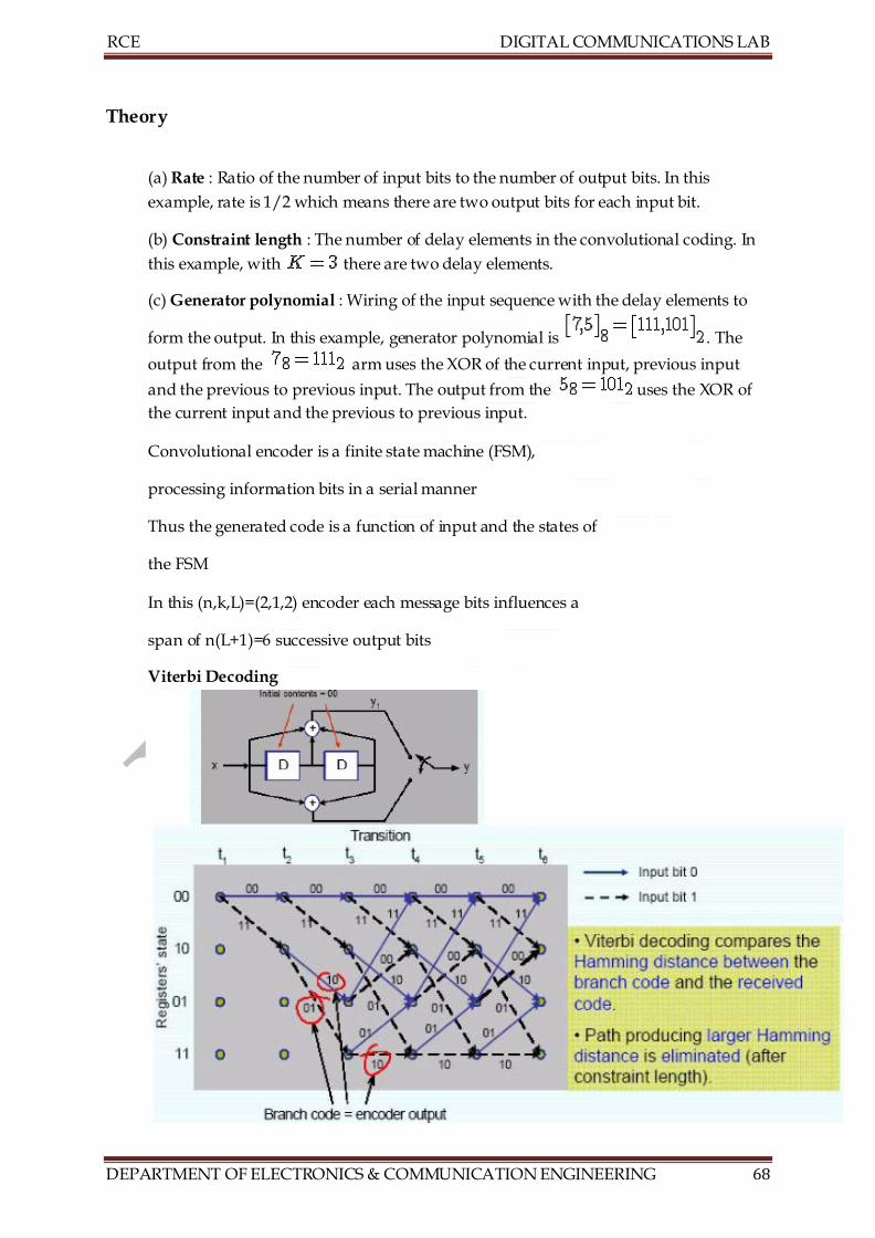
Viterbi Decoding
RCE DIGITAL COMMUNICATIONS LAB
DEPARTMENT OF ELECTRONICS & COMMUNICATION ENGINEERING 69
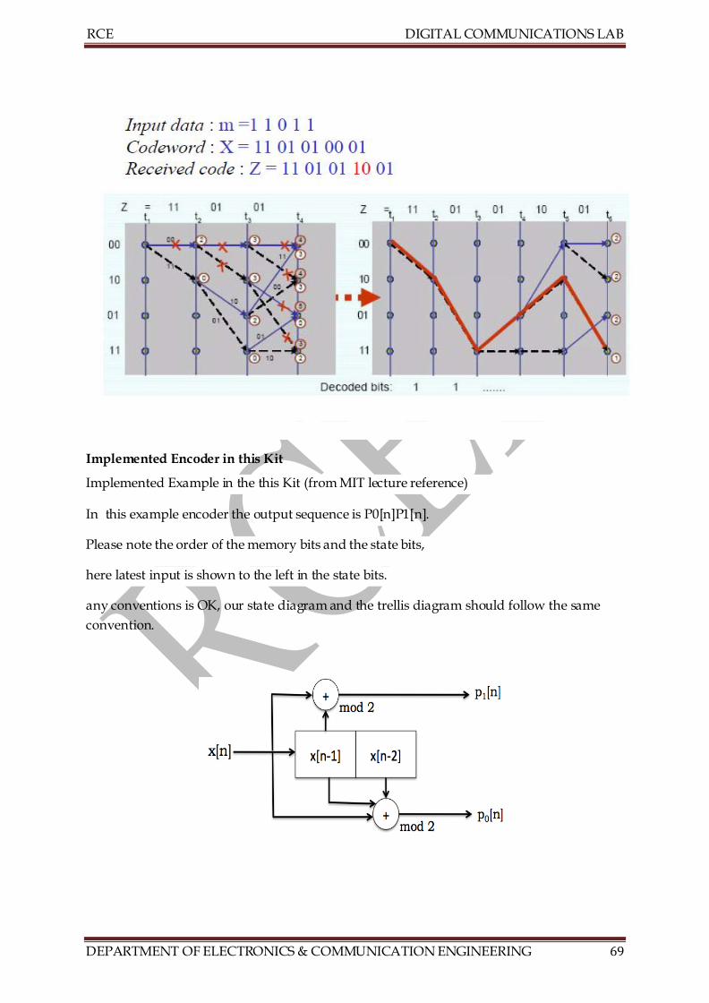
Implemented Encoder in this Kit
Implemented Example in the this Kit (from MIT lecture reference)
In this example encoder the output sequence is P0[n]P1[n].
Please note the order of the memory bits and the state bits,
here latest input is shown to the left in the state bits.
any conventions is OK, our state diagram and the trellis diagram should follow the same
convention.
RCE DIGITAL COMMUNICATIONS LAB
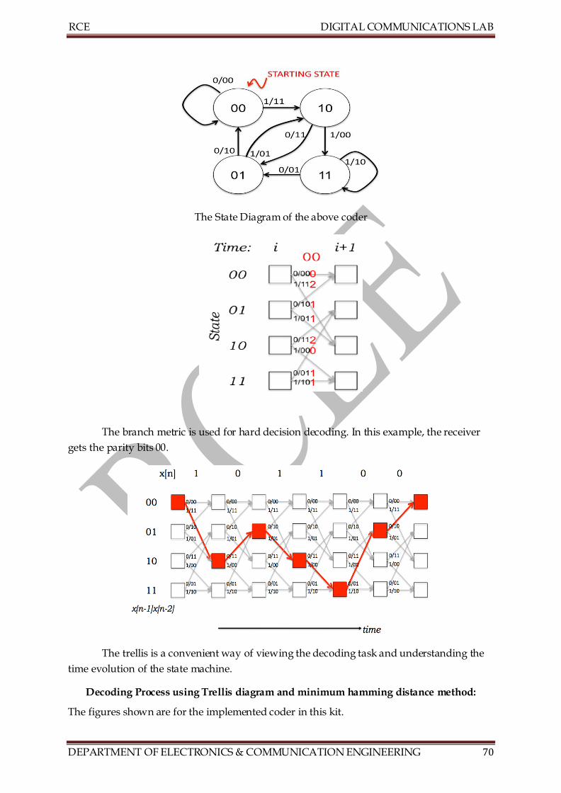
DEPARTMENT OF ELECTRONICS & COMMUNICATION ENGINEERING 70
The State Diagram of the above coder
The branch metric is used for hard decision decoding. In this example, the receiver
gets the parity bits 00.
The trellis is a convenient way of viewing the decoding task and understanding the
time evolution of the state machine.
Decoding Process using Trellis diagram and minimum hamming distance method:
The figures shown are for the implemented coder in this kit.
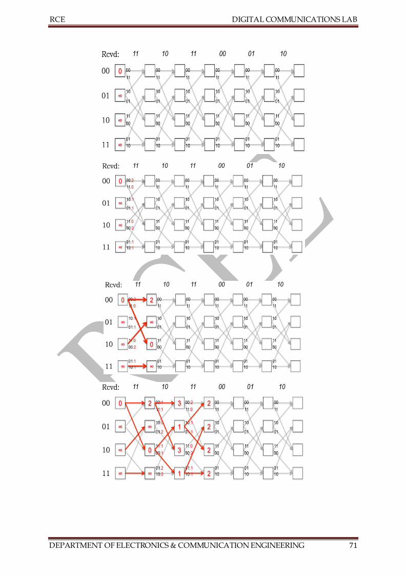
RCE DIGITAL COMMUNICATIONS LAB
DEPARTMENT OF ELECTRONICS & COMMUNICATION ENGINEERING 71
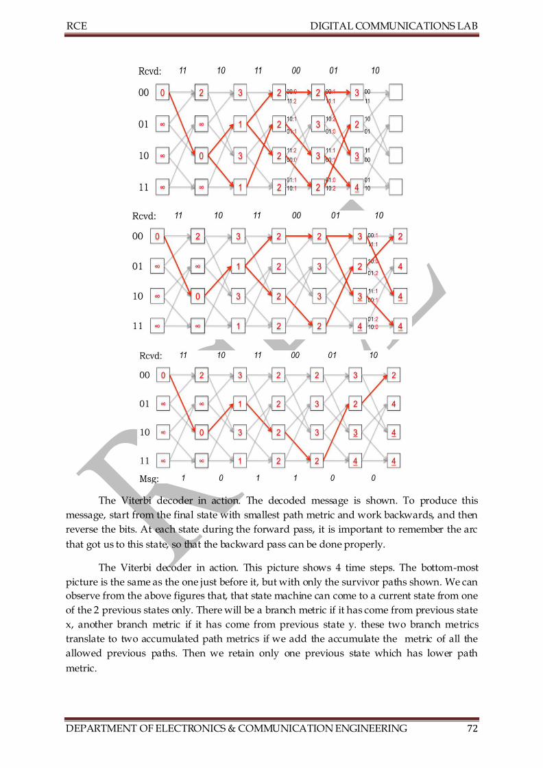
RCE DIGITAL COMMUNICATIONS LAB
DEPARTMENT OF ELECTRONICS & COMMUNICATION ENGINEERING 72
The Viterbi decoder in action. The decoded message is shown. To produce this
message, start from the final state with smallest path metric and work backwards, and then
reverse the bits. At each state during the forward pass, it is important to remember the arc
that got us to this state, so that the backward pass can be done properly.
The Viterbi decoder in action. This picture shows 4 time steps. The bottom-most
picture is the same as the one just before it, but with only the survivor paths shown. We can
observe from the above figures that, that state machine can come to a current state from one
of the 2 previous states only. There will be a branch metric if it has come from previous state
x, another branch metric if it has come from previous state y. these two branch metrics
translate to two accumulated path metrics if we add the accumulate the metric of all the
allowed previous paths. Then we retain only one previous state which has lower path
metric.
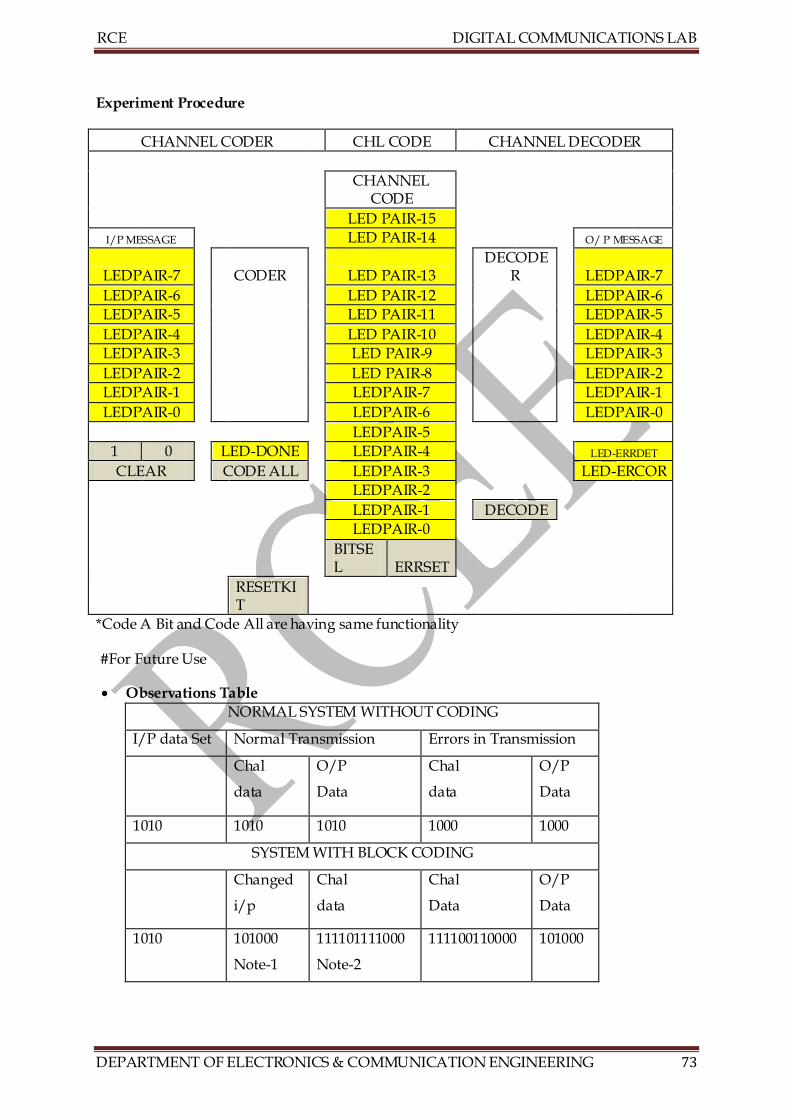
RCE DIGITAL COMMUNICATIONS LAB
DEPARTMENT OF ELECTRONICS & COMMUNICATION ENGINEERING 73
Experiment Procedure
CHANNEL CODER CHL CODE CHANNEL DECODER
CHANNEL CODE
LED PAIR-15
I/P MESSAGE
LED PAIR-14
O/ P MESSAGE
LEDPAIR-7
CODER
LED PAIR-13
DECODER
LEDPAIR-7
LEDPAIR-6
LED PAIR-12
LEDPAIR-6
LEDPAIR-5
LED PAIR-11
LEDPAIR-5
LEDPAIR-4
LED PAIR-10
LEDPAIR-4
LEDPAIR-3
LED PAIR-9
LEDPAIR-3
LEDPAIR-2
LED PAIR-8
LEDPAIR-2
LEDPAIR-1
LEDPAIR-7
LEDPAIR-1
LEDPAIR-0
LEDPAIR-6
LEDPAIR-0
LEDPAIR-5
1 0
LED-DONE
LEDPAIR-4
LED-ERRDET
CLEAR
CODE ALL
LEDPAIR-3
LED-ERCOR
LEDPAIR-2
LEDPAIR-1
DECODE
LEDPAIR-0
BITSEL ERRSET
RESETKIT
*Code A Bit and Code All are having same functionality
#For Future Use
Observations Table
NORMAL SYSTEM WITHOUT CODING
I/P data Set Normal Transmission Errors in Transmission
Chal
data
O/P
Data
Chal
data
O/P
Data
1010 1010 1010 1000 1000
SYSTEM WITH BLOCK CODING
Changed
i/p
Chal
data
Chal
Data
O/P
Data
1010 101000
Note-1
111101111000
Note-2
111100110000 101000
RCE DIGITAL COMMUNICATIONS LAB
DEPARTMENT OF ELECTRONICS & COMMUNICATION ENGINEERING 74
Note-1: Channel input increases such that the memory states should become Zero’s
Note-2:Channel data as per Convolution encoding
Experiment Procedure:
Observe the signal chain , i.e. the input stage, coding stage, transmission stage and the
decode stage
Put the mode selection switch in NORMAL mode and see the process and observe output
Student selects input message that is to be coded, by shifting the bits 0/1 by means of
pressing the keys 0, 1, CLEAR.
Student codes this input message by pushing the key ‘CODE A BIT’ or by pushing
‘CODEALL’. Note that after pressing this the input data gets shifted up and two 00 bits are
added at lower end. This is required in the convolution decoding process, the last two bits
should always be zero , the state should come back to 0 , to decode hence this automatic 0
addition.
Now the message is coded and displayed in the transmission path. Student can now
introduce an error in the transmission channel by means of pressing the keys BITSEL and
ERRSET. On every push of the BITSEL one bit is selected in the channel code, the selected bit
will be completely in OFF mode at this stage, if the student presses ERRSET key, the OFF
mode bit will be inverted to make it as an error.
Now the student pushes the DECODE key, the channel code is decoded and displayed as
the Output message. If an error is detected in the channel code ERRDETECTED LED glows,
if an error is corrected from channel code then the ERRCORRECTED LED glows in the
decoder Output stage.
Now put mode selection in CODE mode and repeat the process and observe the output
changes.
Observe how the error detection and correction in code mode and hence the implementation
of convolution encoder and decoder.
Pushing Demo mode switch will give a brief description of implementation of KIT
Coding Theory Back Ground Information
Terminology Systematic / non-systematic codes
In coding theory, a systematic code is any error-correcting code in which the input data is embedded in the encoded output. Conversely, in a non-systematic code the output does not
contain the input symbols. Linear Code In coding theory, a linear code is an error-correcting code for which any linear combination of codewords is also a codeword. Linear codes are traditionally partitioned
into block codes and convolutional codes, although turbo codes can be seen as a hybrid of these two types.[1]Linear codes allow for more efficient encoding and decoding algorithms than other codes (cf. syndrome decoding).
RCE DIGITAL COMMUNICATIONS LAB
DEPARTMENT OF ELECTRONICS & COMMUNICATION ENGINEERING 75
Block code
In coding theory, block codes refers to the large and important family of error-correcting codes that encode data in blocks. There is a vast number of examples for block codes, many of which have a wide range of practical applications. The main reason why the concept of block codes is so useful is that it allows coding theorists, mathematicians, and computer
scientists to study the limitations of all block codes in a unified way. Such limitations often take the form of bounds that relate different parameters of the block code to each other, such as its rate and its ability to detect and correct errors. Examples of block codes are Reed–Solomon codes, Hamming codes, Hadamard codes, Expander codes, Golay codes, and Reed–Muller codes. These examples also belong to
the class of linear codes, and hence they are called linear block codes. Convolution code In telecommunication, a convolutional code is a type of error-correcting code in which
each m-bit information symbol (each m-bit string) to be encoded is transformed into an n-bit symbol, where m/n is the code rate (n ≥ m) and the transformation is a function of the last k information symbols, where k is the constraint length of the code. Convolution codes are used extensively in numerous applications in order to achieve reliable data transfer, including digital video, radio, mobile communication, and satellite
communication. These codes are often implemented in concatenation with a hard-decision code, particularly Reed Solomon. Prior to turbo codes, such constructions were the most efficient, coming closest to the Shannon limit. Turbo code
Syndrome decoding Viterbi decoding
RCE DIGITAL COMMUNICATIONS LAB
DEPARTMENT OF ELECTRONICS & COMMUNICATION ENGINEERING 76
1 COMPANDING
Aim: To implement of μ-law compression and expansion of a signal.
Equipment Required:
TMS 320XXXX DSP Trainer Kit
PC with MATLAB, CCS
Power supply.
Theory:
At the telephone transmitter, microphone converts human speech to analog
signals. For digital transmission, this analog signal is converted to a digital signal,
which has a fixed precision. To provide higher voice quality at a lower cost, the
analog signals may be converted to digital signals using Pulse Code Modulation
(PCM).
PCM is composed of three successive steps: sampling, quantizing and coding.
Sampling is the determination of a signal’s amplitude at regular time intervals. Since
the telephone network has a bandwidth of 4 kHz, for accurate reproduction, a voice
signal must be sampled at a rate of at least 8 kHz, according to Nyquist’s theorem.
That is, the amplitude of the signal is sampled every 125 µs. Once the signal’s
amplitude is obtained, it is quantized into a discrete set of amplitude levels for
representation as a digital signal. The quantization process introduces quantization
error (- to +) into the digital signal, where ‘’ is the step size; however, the
introduced error may be minimized by minimizing the step size with respect to the
number of bits needed to uniquely identify the quantization levels. The SNR of a
PCM system is depends on the quantization noise power (2/12). Due to the fixed
value of step size the noise power is more for weak amplitudes compare to strong
amplitudes of the signal, results SNR is not constant over entire signal.
Instead of employing uniform quantization, a natural non-uniform substitute
is observed in the human auditory system with a variable step size (). The non-
uniform quantization (variable step size) becomes difficult to implement in practical.
Therefore the signal is amplified at low signal levels and attenuated at high signal levels .
After this process, uniform quantization is used. This is equivalent to more step size
at low signal levels and small step size at high signal levels. At the receiver a reverse
process is done. That is signal is attenuated at low signal levels and amplified at high
signal levels to get original signal. Thus the Compression of signal at transmitter and
Expansion at receiver is called as Companding.
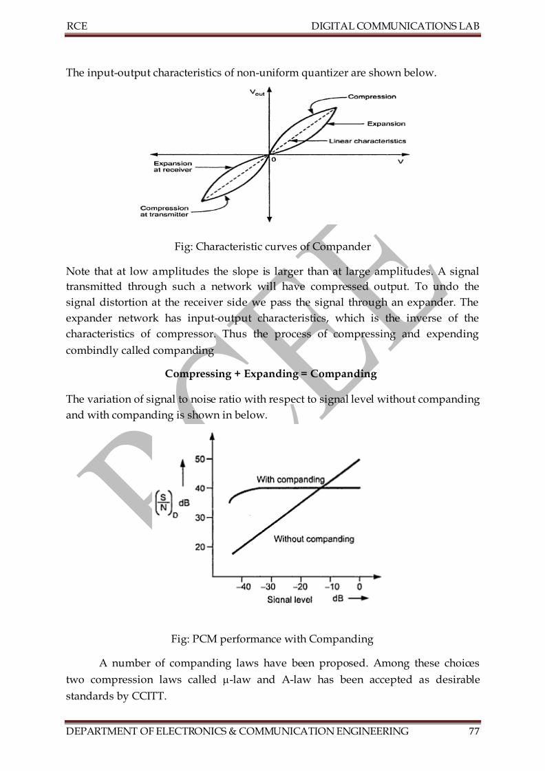
RCE DIGITAL COMMUNICATIONS LAB
DEPARTMENT OF ELECTRONICS & COMMUNICATION ENGINEERING 77
The input-output characteristics of non-uniform quantizer are shown below.
Fig: Characteristic curves of Compander
Note that at low amplitudes the slope is larger than at large amplitudes. A signal
transmitted through such a network will have compressed output. To undo the
signal distortion at the receiver side we pass the signal through an expander. The
expander network has input-output characteristics, which is the inverse of the
characteristics of compressor. Thus the process of compressing and expending
combindly called companding
Compressing + Expanding = Companding
The variation of signal to noise ratio with respect to signal level without companding
and with companding is shown in below.
Fig: PCM performance with Companding
A number of companding laws have been proposed. Among these choices
two compression laws called -law and A-law has been accepted as desirable
standards by CCITT.
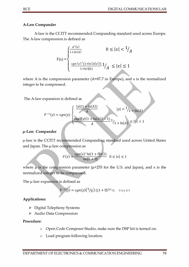
RCE DIGITAL COMMUNICATIONS LAB
DEPARTMENT OF ELECTRONICS & COMMUNICATION ENGINEERING 78
A-Law Compander
A-law is the CCITT recommended Companding standard used across Europe.
The A-law compression is defined as
F(x) =
𝐴∗ 𝑥
1+ln 𝐴 0 ≤ 𝑥 < 1
𝐴
𝑠𝑔𝑛 𝑥 ∗(1+ln 𝐴 𝑥 )
1+ln(𝐴)1
𝐴 ≤ 𝑥 ≤ 1
where A is the compression parameter (A=87.7 in Europe), and x is the normalized
integer to be compressed.
The A-law expansion is defined as
𝐹−1 𝑦 = 𝑠𝑔𝑛(𝑦)
𝑦 (1 + ln 𝐴 )
𝐴 |𝑦| < 1
1 + ln 𝐴
exp( 𝑦 1 + ln 𝐴 − 1)
𝐴1
1 + ln 𝐴 ≤ 𝑦 < 1
-Law Compander
-law is the CCITT recommended Companding standard used across United States
and Japan. The -law compression as
𝐹 𝑥 =𝑠𝑔𝑛 𝑥 ∗ ln 1 + µ 𝑥 )
ln(1 + µ) 0 ≤ 𝑥 ≤ 1
where µ is the compression parameter (µ=255 for the U.S. and Japan), and x is the
normalized integer to be compressed.
The -law expansion is defined as
𝐹−1 𝑦 = 𝑠𝑔𝑛 𝑦 1µ ((1 + µ) 𝑦 -1) -1 ≤ y ≤ 1
Applications:
Digital Telephony Systems
Audio Data Compression
Procedure:
o Open Code Composer Studio, make sure the DSP kit is turned on.
o Load program following location.
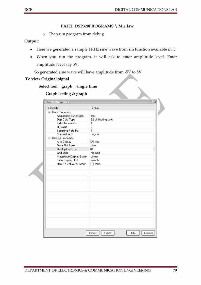
RCE DIGITAL COMMUNICATIONS LAB
DEPARTMENT OF ELECTRONICS & COMMUNICATION ENGINEERING 79
PATH: DSP320PROGRAMS \ Mu_law
o Then run program from debug.
Output:
Here we generated a sample 1KHz sine wave from sin function available in C.
When you run the program, it will ask to enter amplitude level. Enter
amplitude level say 5V.
So generated sine wave will have amplitude from -5V to 5V
To view Original signal
Select tool _ graph _ single time
Graph setting & graph
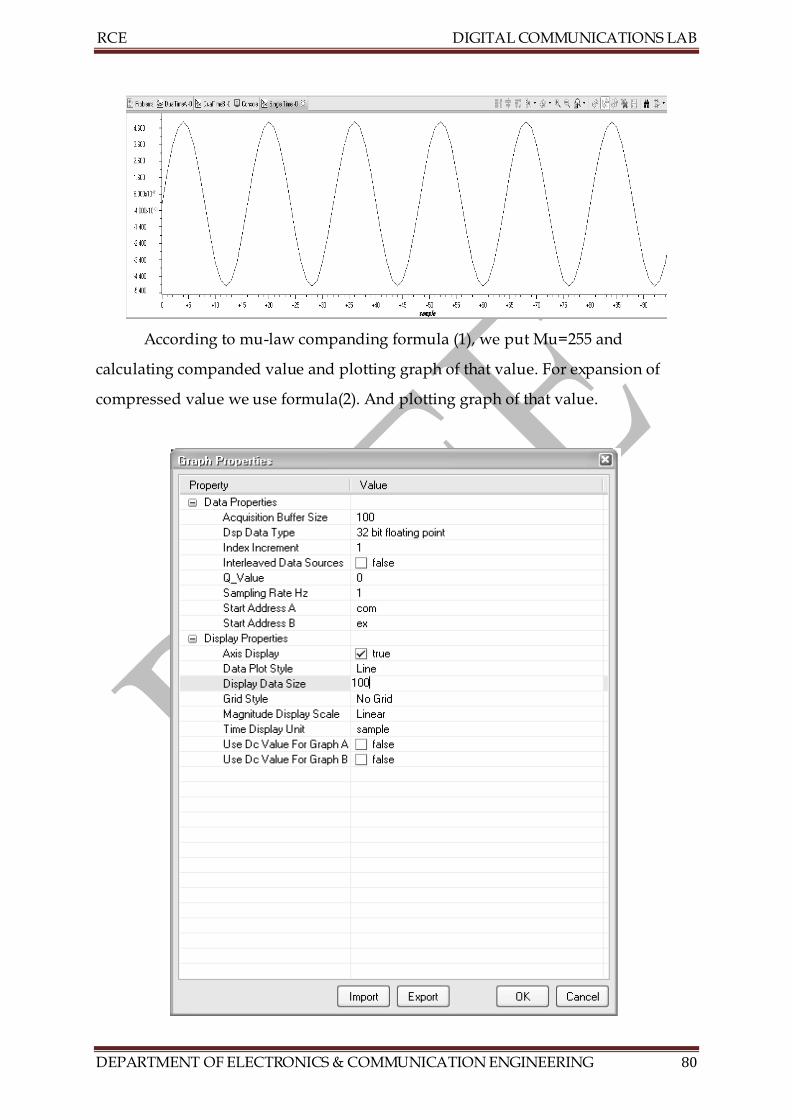
RCE DIGITAL COMMUNICATIONS LAB
DEPARTMENT OF ELECTRONICS & COMMUNICATION ENGINEERING 80
According to mu-law companding formula (1), we put Mu=255 and
calculating companded value and plotting graph of that value. For expansion of
compressed value we use formula(2). And plotting graph of that value.
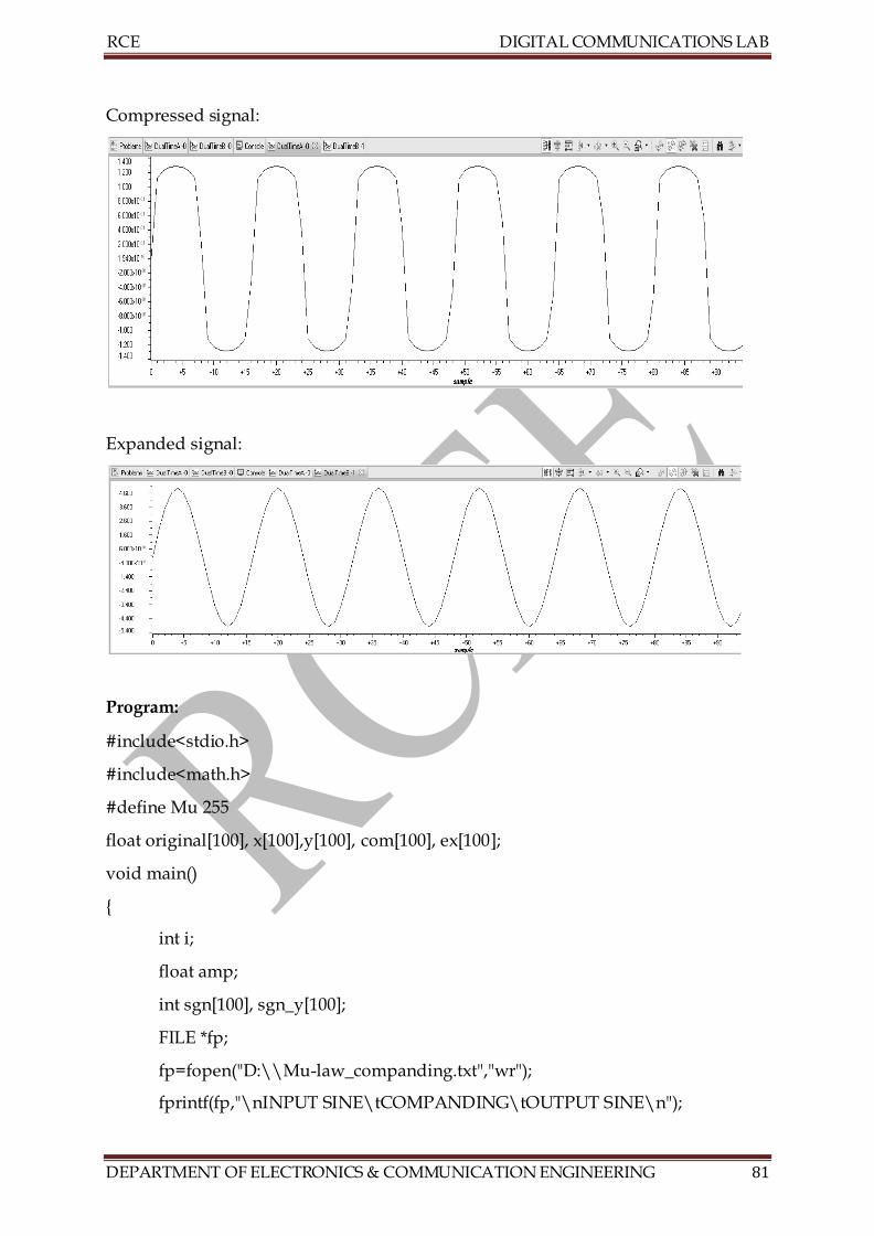
RCE DIGITAL COMMUNICATIONS LAB
DEPARTMENT OF ELECTRONICS & COMMUNICATION ENGINEERING 81
Compressed signal:
Expanded signal:
Program:
#include<stdio.h>
#include<math.h>
#define Mu 255
float original[100], x[100],y[100], com[100], ex[100];
void main()
{
int i;
float amp;
int sgn[100], sgn_y[100];
FILE *fp;
fp=fopen("D:\\Mu-law_companding.txt","wr");
fprintf(fp,"\nINPUT SINE\tCOMPANDING\tOUTPUT SINE\n");
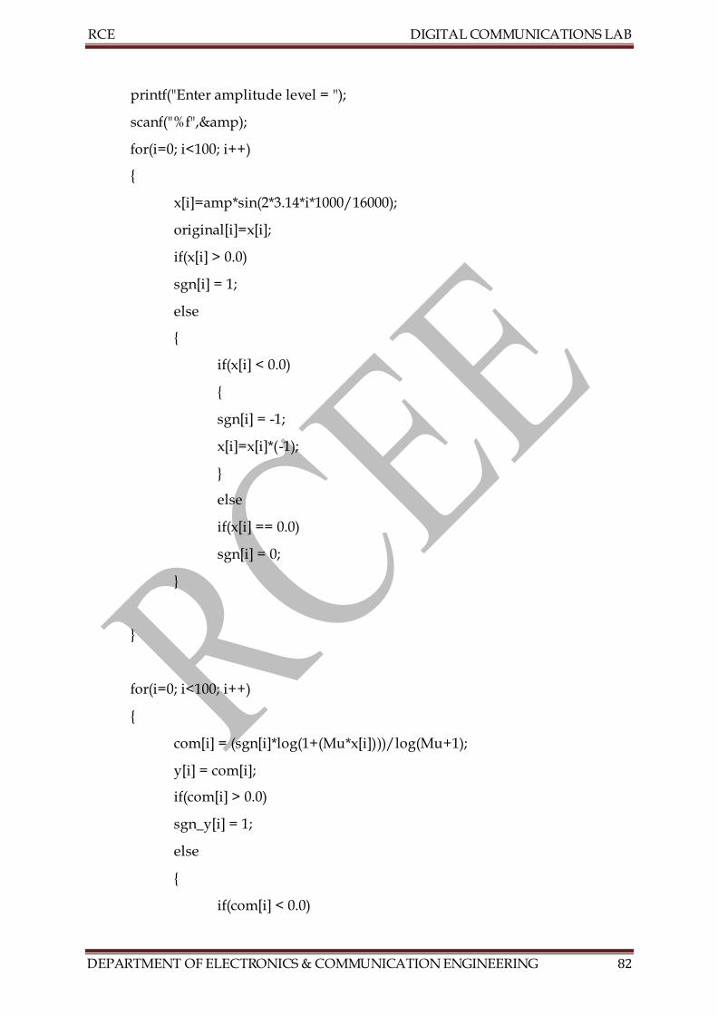
RCE DIGITAL COMMUNICATIONS LAB
DEPARTMENT OF ELECTRONICS & COMMUNICATION ENGINEERING 82
printf("Enter amplitude level = ");
scanf("%f",&);
for(i=0; i<100; i++)
{
x[i]=amp*sin(2*3.14*i*1000/16000);
original[i]=x[i];
if(x[i] > 0.0)
sgn[i] = 1;
else
{
if(x[i] < 0.0)
{
sgn[i] = -1;
x[i]=x[i]*(-1);
}
else
if(x[i] == 0.0)
sgn[i] = 0;
}
}
for(i=0; i<100; i++)
{
com[i] = (sgn[i]*log(1+(Mu*x[i])))/log(Mu+1);
y[i] = com[i];
if(com[i] > 0.0)
sgn_y[i] = 1;
else
{
if(com[i] < 0.0)
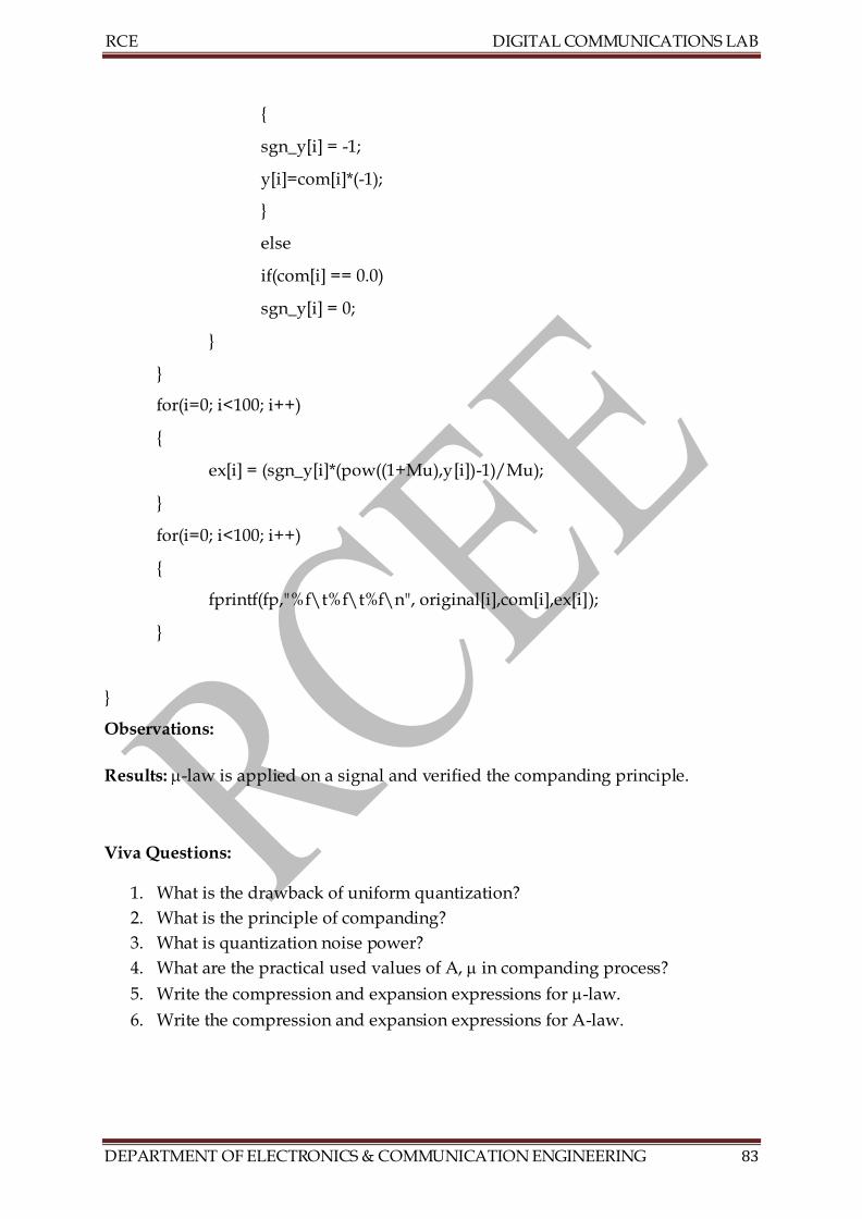
RCE DIGITAL COMMUNICATIONS LAB
DEPARTMENT OF ELECTRONICS & COMMUNICATION ENGINEERING 83
{
sgn_y[i] = -1;
y[i]=com[i]*(-1);
}
else
if(com[i] == 0.0)
sgn_y[i] = 0;
}
}
for(i=0; i<100; i++)
{
ex[i] = (sgn_y[i]*(pow((1+Mu),y[i])-1)/Mu);
}
for(i=0; i<100; i++)
{
fprintf(fp,"%f\t%f\t%f\n", original[i],com[i],ex[i]);
}
}
Observations:
Results: -law is applied on a signal and verified the companding principle.
Viva Questions:
1. What is the drawback of uniform quantization?
2. What is the principle of companding?
3. What is quantization noise power?
4. What are the practical used values of A, in companding process?
5. Write the compression and expansion expressions for -law.
6. Write the compression and expansion expressions for A-law.
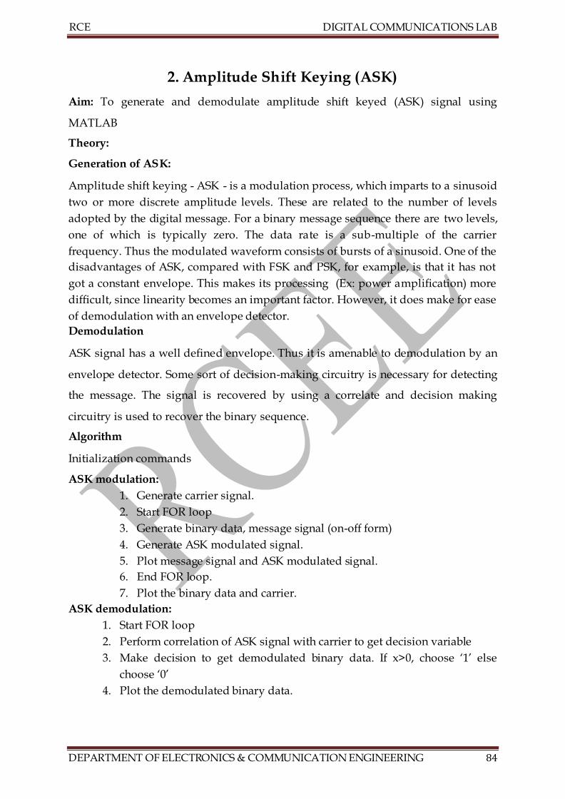
RCE DIGITAL COMMUNICATIONS LAB
DEPARTMENT OF ELECTRONICS & COMMUNICATION ENGINEERING 84
2. Amplitude Shift Keying (ASK)
Aim: To generate and demodulate amplitude shift keyed (ASK) signal using
MATLAB
Theory:
Generation of ASK:
Amplitude shift keying - ASK - is a modulation process, which imparts to a sinusoid
two or more discrete amplitude levels. These are related to the number of levels
adopted by the digital message. For a binary message sequence there are two levels,
one of which is typically zero. The data rate is a sub-multiple of the carrier
frequency. Thus the modulated waveform consists of bursts of a sinusoid. One of the
disadvantages of ASK, compared with FSK and PSK, for example, is that it has not
got a constant envelope. This makes its processing (Ex: power amplification) more
difficult, since linearity becomes an important factor. However, it does make for ease
of demodulation with an envelope detector.
Demodulation
ASK signal has a well defined envelope. Thus it is amenable to demodulation by an
envelope detector. Some sort of decision-making circuitry is necessary for detecting
the message. The signal is recovered by using a correlate and decision making
circuitry is used to recover the binary sequence.
Algorithm
Initialization commands
ASK modulation:
1. Generate carrier signal.
2. Start FOR loop
3. Generate binary data, message signal (on-off form)
4. Generate ASK modulated signal.
5. Plot message signal and ASK modulated signal.
6. End FOR loop.
7. Plot the binary data and carrier.
ASK demodulation:
1. Start FOR loop
2. Perform correlation of ASK signal with carrier to get decision variable
3. Make decision to get demodulated binary data. If x>0, choose ‘1’ else
choose ‘0’
4. Plot the demodulated binary data.
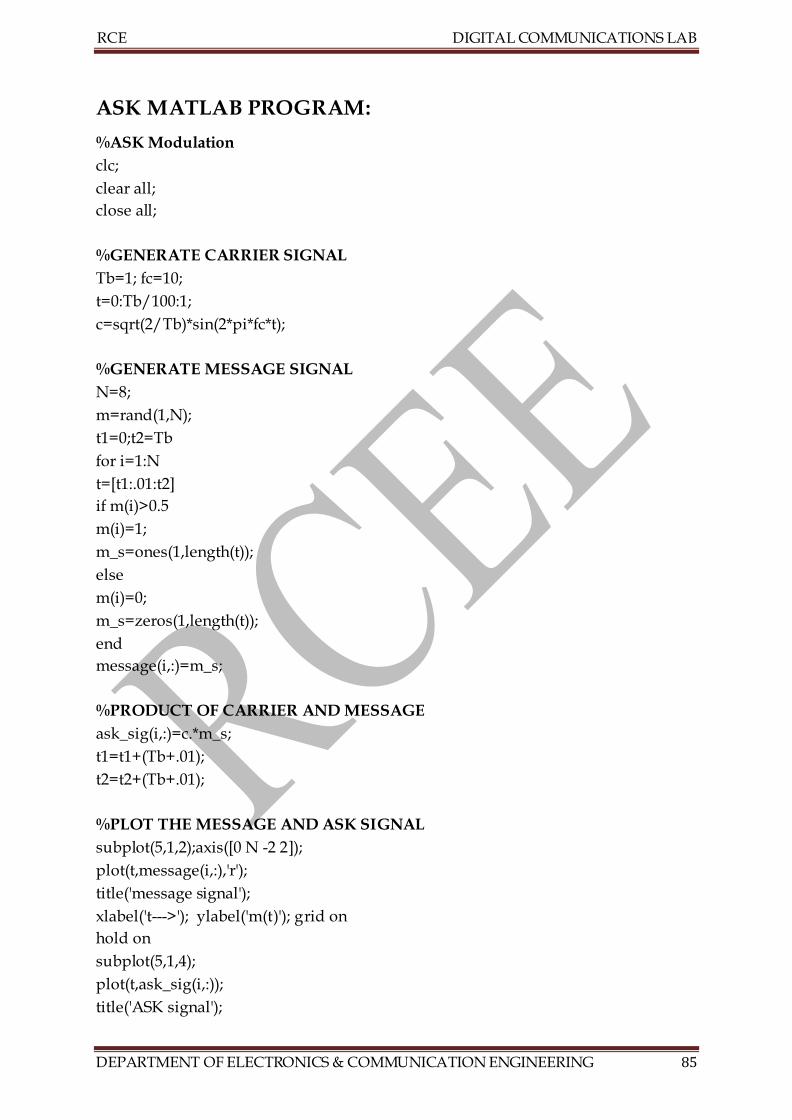
RCE DIGITAL COMMUNICATIONS LAB
DEPARTMENT OF ELECTRONICS & COMMUNICATION ENGINEERING 85
ASK MATLAB PROGRAM:
%ASK Modulation
clc;
clear all;
close all;
%GENERATE CARRIER SIGNAL
Tb=1; fc=10;
t=0:Tb/100:1;
c=sqrt(2/Tb)*sin(2*pi*fc*t);
%GENERATE MESSAGE SIGNAL
N=8;
m=rand(1,N);
t1=0;t2=Tb
for i=1:N
t=[t1:.01:t2]
if m(i)>0.5
m(i)=1;
m_s=ones(1,length(t));
else
m(i)=0;
m_s=zeros(1,length(t));
end
message(i,:)=m_s;
%PRODUCT OF CARRIER AND MESSAGE
ask_sig(i,:)=c.*m_s;
t1=t1+(Tb+.01);
t2=t2+(Tb+.01);
%PLOT THE MESSAGE AND ASK SIGNAL
subplot(5,1,2);axis([0 N -2 2]);
plot(t,message(i,:),'r');
title('message signal');
xlabel('t--->'); ylabel('m(t)'); grid on
hold on
subplot(5,1,4);
plot(t,ask_sig(i,:));
title('ASK signal');
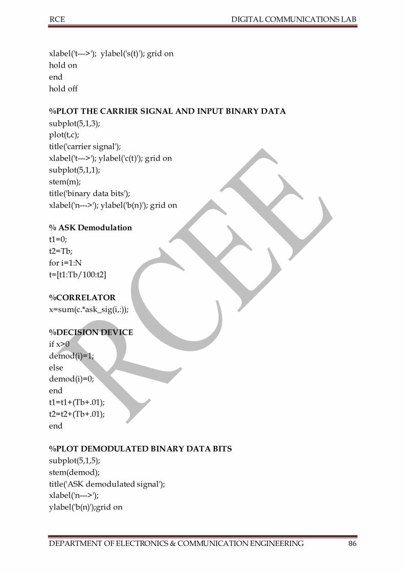
RCE DIGITAL COMMUNICATIONS LAB
DEPARTMENT OF ELECTRONICS & COMMUNICATION ENGINEERING 86
xlabel('t--->'); ylabel('s(t)'); grid on
hold on
end
hold off
%PLOT THE CARRIER SIGNAL AND INPUT BINARY DATA
subplot(5,1,3);
plot(t,c);
title('carrier signal');
xlabel('t--->'); ylabel('c(t)'); grid on
subplot(5,1,1);
stem(m);
title('binary data bits');
xlabel('n--->'); ylabel('b(n)'); grid on
% ASK Demodulation
t1=0;
t2=Tb;
for i=1:N
t=[t1:Tb/100:t2]
%CORRELATOR
x=sum(c.*ask_sig(i,:));
%DECISION DEVICE
if x>0
demod(i)=1;
else
demod(i)=0;
end
t1=t1+(Tb+.01);
t2=t2+(Tb+.01);
end
%PLOT DEMODULATED BINARY DATA BITS
subplot(5,1,5);
stem(demod);
title('ASK demodulated signal');
xlabel('n--->');
ylabel('b(n)');grid on
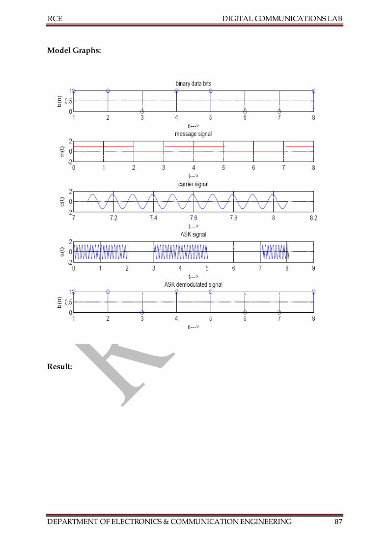
RCE DIGITAL COMMUNICATIONS LAB
DEPARTMENT OF ELECTRONICS & COMMUNICATION ENGINEERING 87
Model Graphs:
Result:
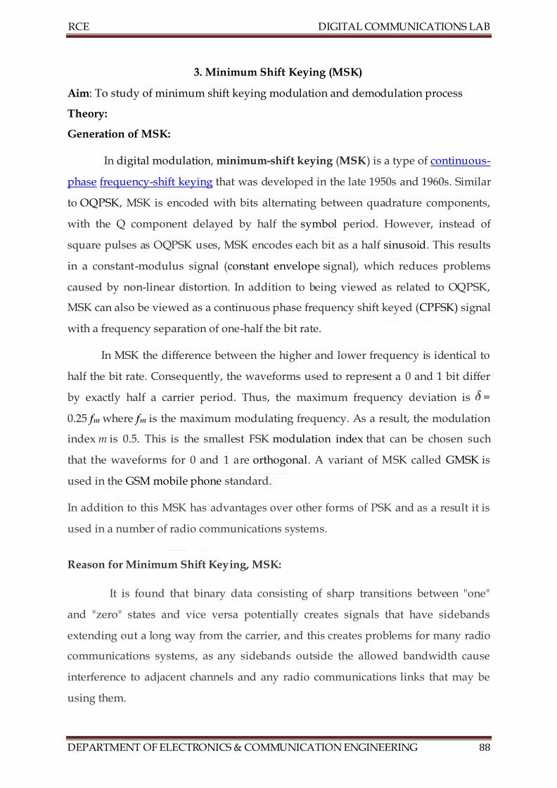
RCE DIGITAL COMMUNICATIONS LAB
DEPARTMENT OF ELECTRONICS & COMMUNICATION ENGINEERING 88
3. Minimum Shift Keying (MSK)
Aim: To study of minimum shift keying modulation and demodulation process
Theory:
Generation of MSK:
In digital modulation, minimum-shift keying (MSK) is a type of continuous-
phase frequency-shift keying that was developed in the late 1950s and 1960s. Similar
to OQPSK, MSK is encoded with bits alternating between quadrature components,
with the Q component delayed by half the symbol period. However, instead of
square pulses as OQPSK uses, MSK encodes each bit as a half sinusoid. This results
in a constant-modulus signal (constant envelope signal), which reduces problems
caused by non-linear distortion. In addition to being viewed as related to OQPSK,
MSK can also be viewed as a continuous phase frequency shift keyed (CPFSK) signal
with a frequency separation of one-half the bit rate.
In MSK the difference between the higher and lower frequency is identical to
half the bit rate. Consequently, the waveforms used to represent a 0 and 1 bit differ
by exactly half a carrier period. Thus, the maximum frequency deviation is =
0.25 fm where fm is the maximum modulating frequency. As a result, the modulation
index m is 0.5. This is the smallest FSK modulation index that can be chosen such
that the waveforms for 0 and 1 are orthogonal. A variant of MSK called GMSK is
used in the GSM mobile phone standard.
In addition to this MSK has advantages over other forms of PSK and as a result it is
used in a number of radio communications systems.
Reason for Minimum Shift Keying, MSK:
It is found that binary data consisting of sharp transitions between "one"
and "zero" states and vice versa potentially creates signals that have sidebands
extending out a long way from the carrier, and this creates problems for many radio
communications systems, as any sidebands outside the allowed bandwidth cause
interference to adjacent channels and any radio communications links that may be
using them.
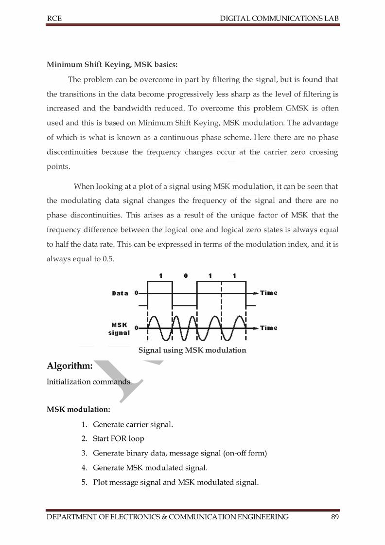
RCE DIGITAL COMMUNICATIONS LAB
DEPARTMENT OF ELECTRONICS & COMMUNICATION ENGINEERING 89
Minimum Shift Keying, MSK basics:
The problem can be overcome in part by filtering the signal, but is found that
the transitions in the data become progressively less sharp as the level of filtering is
increased and the bandwidth reduced. To overcome this problem GMSK is often
used and this is based on Minimum Shift Keying, MSK modulation. The advantage
of which is what is known as a continuous phase scheme. Here there are no phase
discontinuities because the frequency changes occur at the carrier zero crossing
points.
When looking at a plot of a signal using MSK modulation, it can be seen that
the modulating data signal changes the frequency of the signal and there are no
phase discontinuities. This arises as a result of the unique factor of MSK that the
frequency difference between the logical one and logical zero states is always equal
to half the data rate. This can be expressed in terms of the modulation index, and it is
always equal to 0.5.
Signal using MSK modulation
Algorithm:
Initialization commands
MSK modulation:
1. Generate carrier signal.
2. Start FOR loop
3. Generate binary data, message signal (on-off form)
4. Generate MSK modulated signal.
5. Plot message signal and MSK modulated signal.
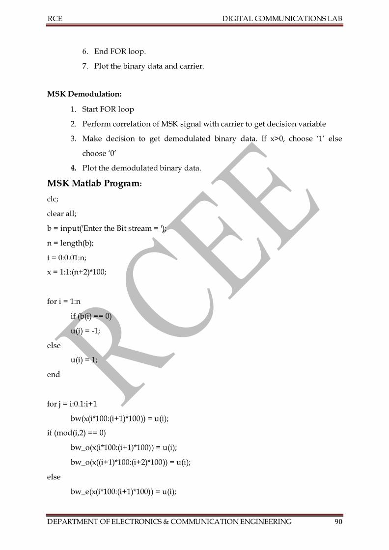
RCE DIGITAL COMMUNICATIONS LAB
DEPARTMENT OF ELECTRONICS & COMMUNICATION ENGINEERING 90
6. End FOR loop.
7. Plot the binary data and carrier.
MSK Demodulation:
1. Start FOR loop
2. Perform correlation of MSK signal with carrier to get decision variable
3. Make decision to get demodulated binary data. If x>0, choose ‘1’ else
choose ‘0’
4. Plot the demodulated binary data.
MSK Matlab Program:
clc;
clear all;
b = input('Enter the Bit stream = ');
n = length(b);
t = 0:0.01:n;
x = 1:1:(n+2)*100;
for i = 1:n
if (b(i) == 0)
u(i) = -1;
else
u(i) = 1;
end
for j = i:0.1:i+1
bw(x(i*100:(i+1)*100)) = u(i);
if (mod(i,2) == 0)
bw_o(x(i*100:(i+1)*100)) = u(i);
bw_o(x((i+1)*100:(i+2)*100)) = u(i);
else
bw_e(x(i*100:(i+1)*100)) = u(i);
RCE DIGITAL COMMUNICATIONS LAB
DEPARTMENT OF ELECTRONICS & COMMUNICATION ENGINEERING 91
bw_e(x((i+1)*100:(i+2)*100)) = u(i);
end
if (mod(n,2)~= 0)
bw_o(x(n*100:(n+1)*100)) = -1;
bw_o(x((n+1)*100:(n+2)*100)) = -1;
end
end
end
bw = bw(100:end);
bw_e = bw_e(100:(n+1)*100);
bw_o = bw_o(200:(n+2)*100);
wo = 2*pi*t*(5/4);
Wt = 2*pi*t/(4*1);
st = bw_o.*sin(wo+(bw_e.*bw_o).*Wt);
subplot(4,1,1);
plot(t,bw);
xlabel('Time ---->'); ylabel('Amplitude ---->');
title('Input Bit Stream'); grid on; axis([0 n -2 +2]);
subplot(4,1,2);
plot(t,bw_o);
xlabel('Time ---->'); ylabel('Amplitude ---->');
title('Odd Sequence'); grid on; axis([0 n -2 +2]);
subplot(4,1,3);
plot(t,bw_e);
xlabel('Time ---->'); ylabel('Amplitude ---->');
title('Even Sequence'); grid on; axis([0 n -2 +2]);
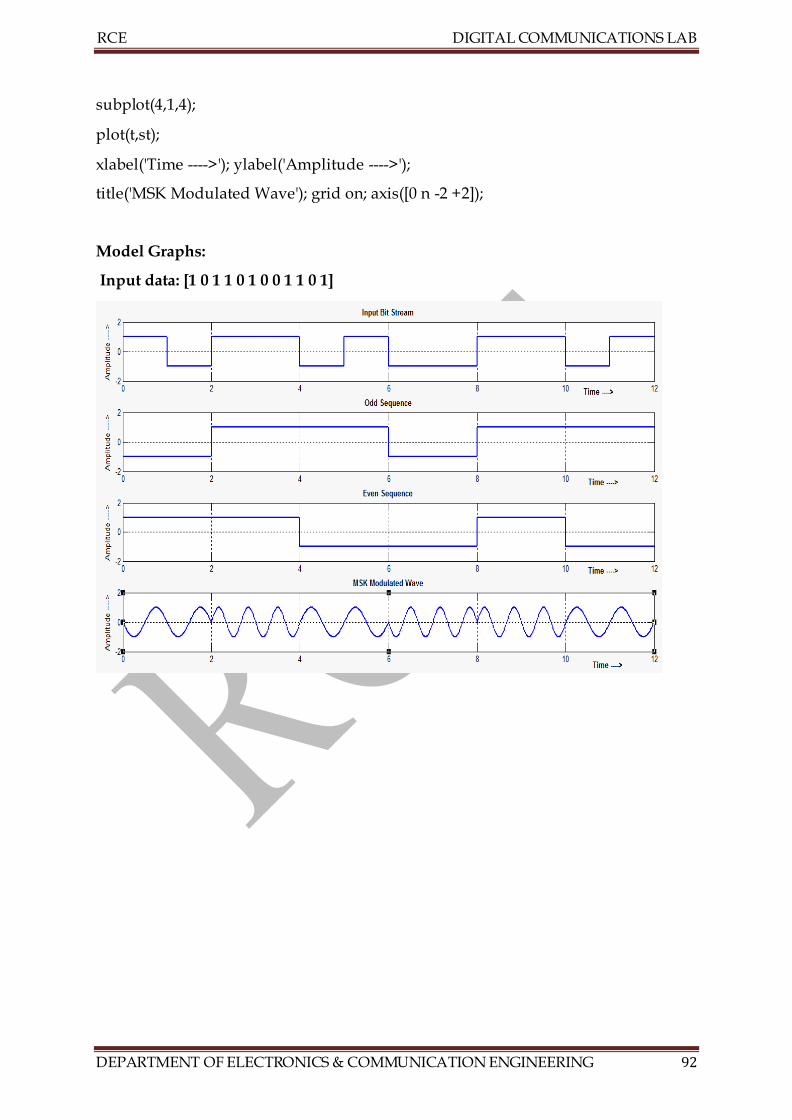
RCE DIGITAL COMMUNICATIONS LAB
DEPARTMENT OF ELECTRONICS & COMMUNICATION ENGINEERING 92
subplot(4,1,4);
plot(t,st);
xlabel('Time ---->'); ylabel('Amplitude ---->');
title('MSK Modulated Wave'); grid on; axis([0 n -2 +2]);
Model Graphs:
Input data: [1 0 1 1 0 1 0 0 1 1 0 1]
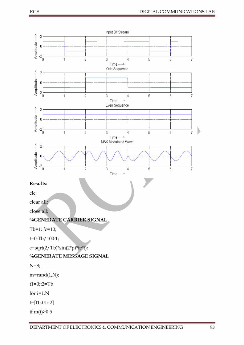
RCE DIGITAL COMMUNICATIONS LAB
DEPARTMENT OF ELECTRONICS & COMMUNICATION ENGINEERING 93
Results:
clc;
clear all;
close all;
%GENERATE CARRIER SIGNAL
Tb=1; fc=10;
t=0:Tb/100:1;
c=sqrt(2/Tb)*sin(2*pi*fc*t);
%GENERATE MESSAGE SIGNAL
N=8;
m=rand(1,N);
t1=0;t2=Tb
for i=1:N
t=[t1:.01:t2]
if m(i)>0.5
RCE DIGITAL COMMUNICATIONS LAB
DEPARTMENT OF ELECTRONICS & COMMUNICATION ENGINEERING 94
m(i)=1;
m_s=ones(1,length(t));
else
m(i)=0;
m_s=zeros(1,length(t));
end
message(i,:)=m_s;
%PRODUCT OF CARRIER AND MESSAGE
ask_sig(i,:)=c.*m_s;
t1=t1+(Tb+.01);
t2=t2+(Tb+.01);
%PLOT THE MESSAGE AND ASK SIGNAL
subplot(5,1,2);axis([0 N -2 2]);
plot(t,message(i,:),'r');
title('message signal');
xlabel('t--->'); ylabel('m(t)'); grid on
hold on
subplot(5,1,4);
plot(t,ask_sig(i,:));
title('ASK signal');
xlabel('t--->'); ylabel('s(t)'); grid on
hold on
end
hold off
%PLOT THE CARRIER SIGNAL AND INPUT BINARY DATA
subplot(5,1,3);
plot(t,c);
title('carrier signal');
xlabel('t--->'); ylabel('c(t)'); grid on
subplot(5,1,1);
stem(m);
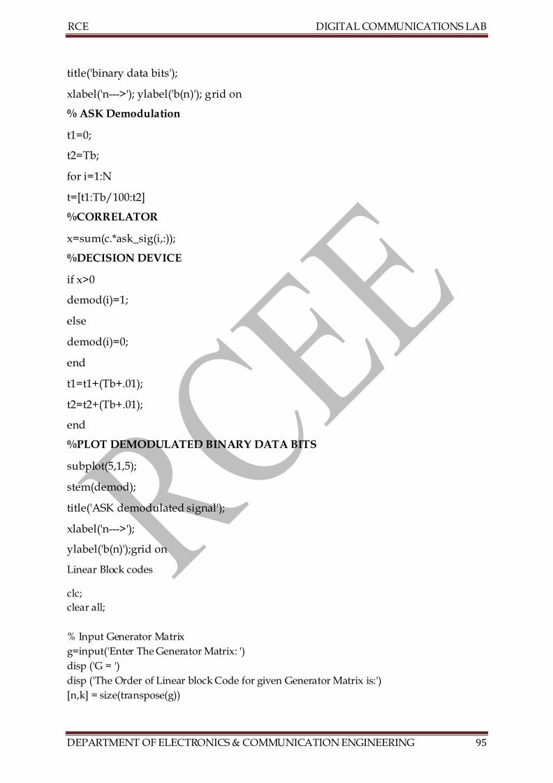
RCE DIGITAL COMMUNICATIONS LAB
DEPARTMENT OF ELECTRONICS & COMMUNICATION ENGINEERING 95
title('binary data bits');
xlabel('n--->'); ylabel('b(n)'); grid on
% ASK Demodulation
t1=0;
t2=Tb;
for i=1:N
t=[t1:Tb/100:t2]
%CORRELATOR
x=sum(c.*ask_sig(i,:));
%DECISION DEVICE
if x>0
demod(i)=1;
else
demod(i)=0;
end
t1=t1+(Tb+.01);
t2=t2+(Tb+.01);
end
%PLOT DEMODULATED BINARY DATA BITS
subplot(5,1,5);
stem(demod);
title('ASK demodulated signal');
xlabel('n--->');
ylabel('b(n)');grid on
Linear Block codes
clc;
clear all;
% Input Generator Matrix
g=input('Enter The Generator Matrix: ')
disp ('G = ')
disp ('The Order of Linear block Code for given Generator Matrix is:')
[n,k] = size(transpose(g))
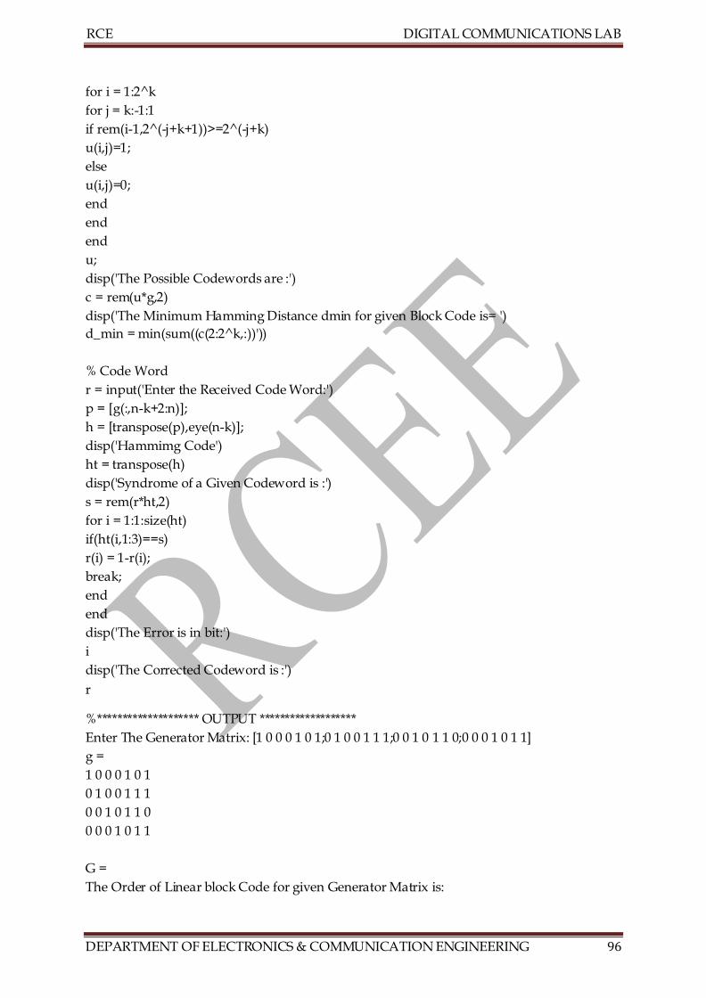
RCE DIGITAL COMMUNICATIONS LAB
DEPARTMENT OF ELECTRONICS & COMMUNICATION ENGINEERING 96
for i = 1:2^k
for j = k:-1:1
if rem(i-1,2^(-j+k+1))>=2^(-j+k)
u(i,j)=1;
else
u(i,j)=0;
end
end
end
u;
disp('The Possible Codewords are :')
c = rem(u*g,2)
disp('The Minimum Hamming Distance dmin for given Block Code is= ')
d_min = min(sum((c(2:2^k,:))'))
% Code Word
r = input('Enter the Received Code Word:')
p = [g(:,n-k+2:n)];
h = [transpose(p),eye(n-k)];
disp('Hammimg Code')
ht = transpose(h)
disp('Syndrome of a Given Codeword is :')
s = rem(r*ht,2)
for i = 1:1:size(ht)
if(ht(i,1:3)==s)
r(i) = 1-r(i);
break;
end
end
disp('The Error is in bit:')
i
disp('The Corrected Codeword is :')
r
%******************** OUTPUT *******************
Enter The Generator Matrix: [1 0 0 0 1 0 1;0 1 0 0 1 1 1;0 0 1 0 1 1 0;0 0 0 1 0 1 1]
g =
1 0 0 0 1 0 1
0 1 0 0 1 1 1
0 0 1 0 1 1 0
0 0 0 1 0 1 1
G =
The Order of Linear block Code for given Generator Matrix is:
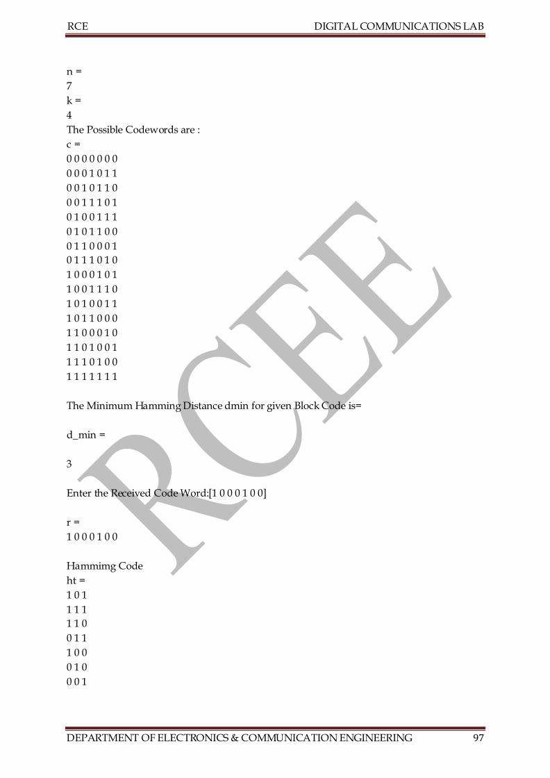
RCE DIGITAL COMMUNICATIONS LAB
DEPARTMENT OF ELECTRONICS & COMMUNICATION ENGINEERING 97
n =
7
k =
4
The Possible Codewords are :
c =
0 0 0 0 0 0 0
0 0 0 1 0 1 1
0 0 1 0 1 1 0
0 0 1 1 1 0 1
0 1 0 0 1 1 1
0 1 0 1 1 0 0
0 1 1 0 0 0 1
0 1 1 1 0 1 0
1 0 0 0 1 0 1
1 0 0 1 1 1 0
1 0 1 0 0 1 1
1 0 1 1 0 0 0
1 1 0 0 0 1 0
1 1 0 1 0 0 1
1 1 1 0 1 0 0
1 1 1 1 1 1 1
The Minimum Hamming Distance dmin for given Block Code is=
d_min =
3
Enter the Received Code Word:[1 0 0 0 1 0 0]
r =
1 0 0 0 1 0 0
Hammimg Code
ht =
1 0 1
1 1 1
1 1 0
0 1 1
1 0 0
0 1 0
0 0 1
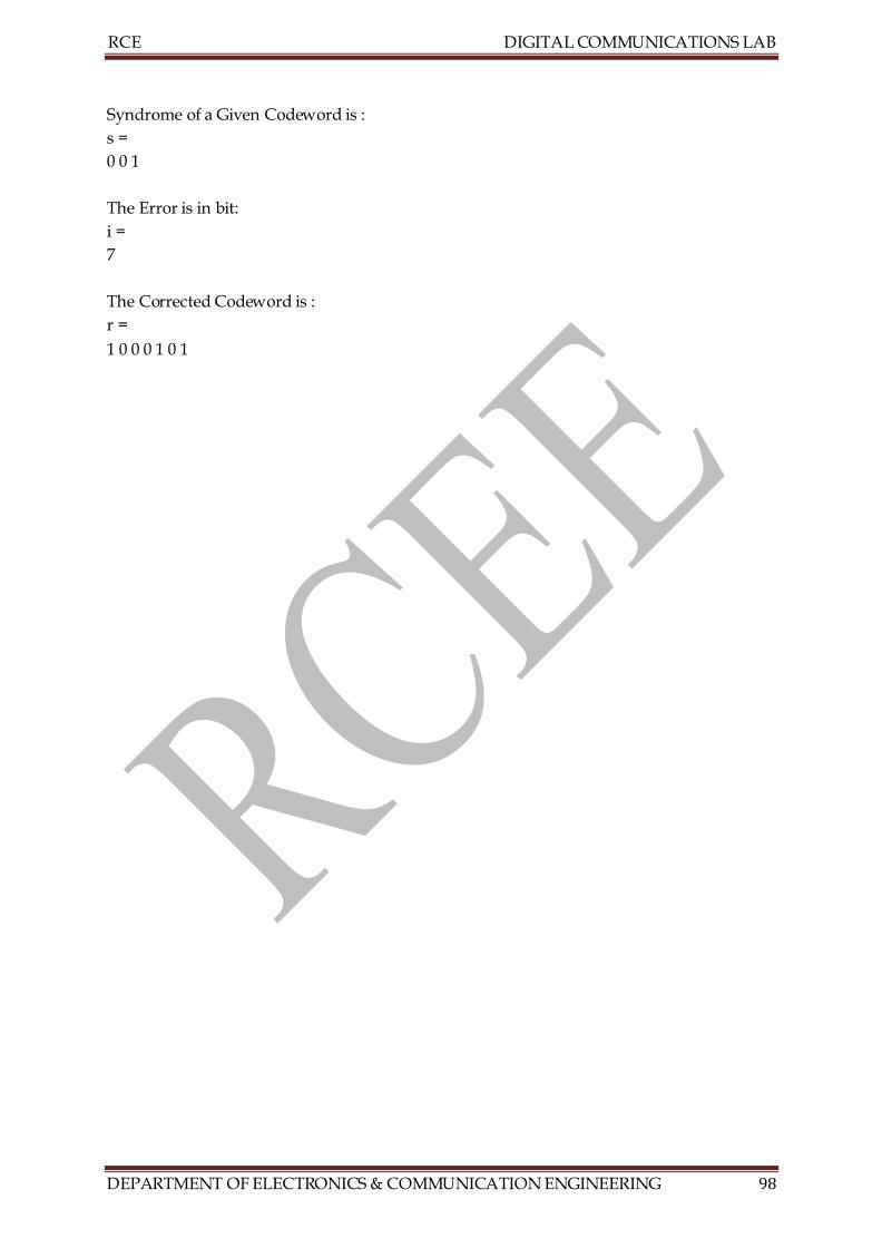
RCE DIGITAL COMMUNICATIONS LAB
DEPARTMENT OF ELECTRONICS & COMMUNICATION ENGINEERING 98
Syndrome of a Given Codeword is :
s =
0 0 1
The Error is in bit:
i =
7
The Corrected Codeword is :
r =
1 0 0 0 1 0 1
Related Documents