Quiescent Signal Analysis 2 0740-7475/06/$20.00 © 2006 IEEE Copublished by the IEEE CS and the IEEE CASS IEEE Design & Test of Computers AS SILICON TECHNOLOGY MOVES forward, back- ground leakage current continues to increase. This trend reduces the effectiveness of traditional I DDQ testing meth- ods and poses a challenge for newer, alternative strate- gies. 1 Alternative methods rely on a self-relative or differential analysis, which factors each chip’s average I DDQ into the pass-fail threshold. Although application of these techniques to low-power chips will continue, they will be increasingly less effective for high-performance ASICs with high background leakage currents. An alternate strategy that could have better scaling properties is to measure the I IDDQ from each of the indi- vidual power ports. In this case, the total leakage current of the chip is distributed across a set of simultaneous measurements. Our method, called quiescent-signal analysis (QSA), exploits this type of measurement scheme to increase the ratio of defect current to leak- age current. Other publications describe a secondary diagnostic benefit of this technique. 2-5 In previous work, we developed several statistic- based methods for processing data collected from simultaneous measurements. We developed a linear regression analysis procedure and applied it to simu- lation data obtained from a commercial power grid. 6 A hyperbola-based method performs defect detection using transient-signal measurements. 7 These techniques analyze multiple simultaneous measurements to accom- plish three goals: detect local signal variations introduced by defects at point sources in the layout, reduce the adverse impact of background leakage current, and diminish the adverse effects of within-die and between-die process variations. In this article, we apply linear regression analysis and a new technique called ellipse analysis to the data collected from a set of 12 test chips to illustrate QSA’s defect detection capabilities and limitations. The test chips, which Jim Plusquellic designed while on sabbatical at IBM Austin Research Laboratory, were fabricated in a 65-nm, 10-metal-layer technolo- gy. They incorporate an array of test structures that let us emulate a defect in one or more of 4,000 distinct chip locations. The design permits control over the magnitude of the emulated-defect current and the leakage current. In particular, we show that regression analysis applied to the data from 21,600 emulated defects detect- ed 99.4 percent of the emulated defects with less than 0.9 percent yield loss. Regression performed better than ellipse analysis, with results of 94.6 percent and 4.8 per- cent for detection and yield loss, respectively. However, with a restricted defect-free data set, ellipse analysis detected 99.7 percent of the emulated defects with no yield loss. Detection sensitivity as well as the level of confidence in the detection decision strongly correlate with the emulated defect’s position in the layout. Both of these measures relate inversely to the distance Quiescent-Signal Analysis: A Multiple Supply Pad I DDQ Method Increasing leakage current makes single-threshold I DDQ testing ineffective for differentiating defective and defect-free chips. Quiescent-signal analysis is a new detection and diagnosis technique that uses I DDQ measurements at multiple chip supply ports, reducing the leakage component in each measurement and significantly improving detection of subtle defects. The authors apply regression and ellipse analysis to data collected from 12 test chips to evaluate the technique. Jim Plusquellic, Dhruva Acharyya, Abhishek Singh, Mohammad Tehranipoor, and Chintan Patel University of Maryland, Baltimore

Welcome message from author
This document is posted to help you gain knowledge. Please leave a comment to let me know what you think about it! Share it to your friends and learn new things together.
Transcript
Quiescent Signal Analysis
2 0740-7475/06/$20.00 © 2006 IEEE Copublished by the IEEE CS and the IEEE CASS IEEE Design & Test of Computers
AS SILICON TECHNOLOGY MOVES forward, back-
ground leakage current continues to increase. This trend
reduces the effectiveness of traditional IDDQ testing meth-
ods and poses a challenge for newer, alternative strate-
gies.1 Alternative methods rely on a self-relative or
differential analysis, which factors each chip’s average
IDDQ into the pass-fail threshold. Although application of
these techniques to low-power chips will continue, they
will be increasingly less effective for high-performance
ASICs with high background leakage currents.
An alternate strategy that could have better scaling
properties is to measure the IIDDQ from each of the indi-
vidual power ports. In this case, the total leakage current
of the chip is distributed across a set of simultaneous
measurements. Our method, called quiescent-signal
analysis (QSA), exploits this type of measurement
scheme to increase the ratio of defect current to leak-
age current. Other publications describe a secondary
diagnostic benefit of this technique.2-5
In previous work, we developed several statistic-
based methods for processing data collected from
simultaneous measurements. We developed a linear
regression analysis procedure and applied it to simu-
lation data obtained from a commercial power grid.6
A hyperbola-based method performs defect detection
using transient-signal measurements.7
These techniques analyze multiple
simultaneous measurements to accom-
plish three goals: detect local signal
variations introduced by defects at
point sources in the layout, reduce the
adverse impact of background leakage
current, and diminish the adverse
effects of within-die and between-die
process variations.
In this article, we apply linear regression analysis
and a new technique called ellipse analysis to the
data collected from a set of 12 test chips to illustrate
QSA’s defect detection capabilities and limitations.
The test chips, which Jim Plusquellic designed while
on sabbatical at IBM Austin Research Laboratory,
were fabricated in a 65-nm, 10-metal-layer technolo-
gy. They incorporate an array of test structures that let
us emulate a defect in one or more of 4,000 distinct
chip locations. The design permits control over the
magnitude of the emulated-defect current and the
leakage current.
In particular, we show that regression analysis
applied to the data from 21,600 emulated defects detect-
ed 99.4 percent of the emulated defects with less than
0.9 percent yield loss. Regression performed better than
ellipse analysis, with results of 94.6 percent and 4.8 per-
cent for detection and yield loss, respectively. However,
with a restricted defect-free data set, ellipse analysis
detected 99.7 percent of the emulated defects with no
yield loss. Detection sensitivity as well as the level of
confidence in the detection decision strongly correlate
with the emulated defect’s position in the layout. Both
of these measures relate inversely to the distance
Quiescent-Signal Analysis: A Multiple Supply Pad IDDQMethod
Increasing leakage current makes single-threshold IDDQ testing ineffective fordifferentiating defective and defect-free chips. Quiescent-signal analysis is anew detection and diagnosis technique that uses IDDQ measurements atmultiple chip supply ports, reducing the leakage component in eachmeasurement and significantly improving detection of subtle defects. Theauthors apply regression and ellipse analysis to data collected from 12 testchips to evaluate the technique.
Jim Plusquellic, Dhruva Acharyya, Abhishek Singh,Mohammad Tehranipoor, and Chintan PatelUniversity of Maryland, Baltimore
between the emulated defect and the nearest neigh-
boring VDD. (The “Related work” sidebar reviews other
proposed techniques for handling the background leak-
age current problem.)
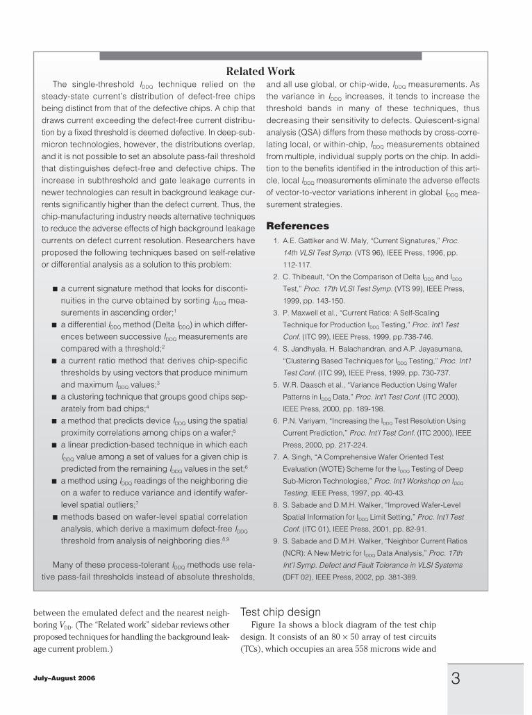
Test chip designFigure 1a shows a block diagram of the test chip
design. It consists of an 80 × 50 array of test circuits
(TCs), which occupies an area 558 microns wide and
3July–August 2006
The single-threshold IDDQ technique relied on thesteady-state current’s distribution of defect-free chipsbeing distinct from that of the defective chips. A chip thatdraws current exceeding the defect-free current distribu-tion by a fixed threshold is deemed defective. In deep-sub-micron technologies, however, the distributions overlap,and it is not possible to set an absolute pass-fail thresholdthat distinguishes defect-free and defective chips. Theincrease in subthreshold and gate leakage currents innewer technologies can result in background leakage cur-rents significantly higher than the defect current. Thus, thechip-manufacturing industry needs alternative techniquesto reduce the adverse effects of high background leakagecurrents on defect current resolution. Researchers haveproposed the following techniques based on self-relativeor differential analysis as a solution to this problem:
■ a current signature method that looks for disconti-nuities in the curve obtained by sorting IDDQ mea-surements in ascending order;1
■ a differential IDDQ method (Delta IDDQ) in which differ-ences between successive IDDQ measurements arecompared with a threshold;2
■ a current ratio method that derives chip-specificthresholds by using vectors that produce minimumand maximum IDDQ values;3
■ a clustering technique that groups good chips sep-arately from bad chips;4
■ a method that predicts device IDDQ using the spatialproximity correlations among chips on a wafer;5
■ a linear prediction-based technique in which eachIDDQ value among a set of values for a given chip ispredicted from the remaining IDDQ values in the set;6
■ a method using IDDQ readings of the neighboring dieon a wafer to reduce variance and identify wafer-level spatial outliers;7
■ methods based on wafer-level spatial correlationanalysis, which derive a maximum defect-free IDDQ
threshold from analysis of neighboring dies.8,9
Many of these process-tolerant IDDQ methods use rela-tive pass-fail thresholds instead of absolute thresholds,
and all use global, or chip-wide, IDDQ measurements. Asthe variance in IDDQ increases, it tends to increase thethreshold bands in many of these techniques, thusdecreasing their sensitivity to defects. Quiescent-signalanalysis (QSA) differs from these methods by cross-corre-lating local, or within-chip, IDDQ measurements obtainedfrom multiple, individual supply ports on the chip. In addi-tion to the benefits identified in the introduction of this arti-cle, local IDDQ measurements eliminate the adverse effectsof vector-to-vector variations inherent in global IDDQ mea-surement strategies.
References1. A.E. Gattiker and W. Maly, “Current Signatures,” Proc.
14th VLSI Test Symp. (VTS 96), IEEE Press, 1996, pp.
112-117.
2. C. Thibeault, “On the Comparison of Delta IDDQ and IDDQ
Test,” Proc. 17th VLSI Test Symp. (VTS 99), IEEE Press,
1999, pp. 143-150.
3. P. Maxwell et al., “Current Ratios: A Self-Scaling
Technique for Production IDDQ Testing,” Proc. Int’l Test
Conf. (ITC 99), IEEE Press, 1999, pp.738-746.
4. S. Jandhyala, H. Balachandran, and A.P. Jayasumana,
“Clustering Based Techniques for IDDQ Testing,” Proc. Int’l
Test Conf. (ITC 99), IEEE Press, 1999, pp. 730-737.
5. W.R. Daasch et al., “Variance Reduction Using Wafer
Patterns in IDDQ Data,” Proc. Int’l Test Conf. (ITC 2000),
IEEE Press, 2000, pp. 189-198.
6. P.N. Variyam, “Increasing the IDDQ Test Resolution Using
Current Prediction,” Proc. Int’l Test Conf. (ITC 2000), IEEE
Press, 2000, pp. 217-224.
7. A. Singh, “A Comprehensive Wafer Oriented Test
Evaluation (WOTE) Scheme for the IDDQ Testing of Deep
Sub-Micron Technologies,” Proc. Int’l Workshop on IDDQ
Testing, IEEE Press, 1997, pp. 40-43.
8. S. Sabade and D.M.H. Walker, “Improved Wafer-Level
Spatial Information for IDDQ Limit Setting,” Proc. Int’l Test
Conf. (ITC 01), IEEE Press, 2001, pp. 82-91.
9. S. Sabade and D.M.H. Walker, “Neighbor Current Ratios
(NCR): A New Metric for IDDQ Data Analysis,” Proc. 17th
Int’l Symp. Defect and Fault Tolerance in VLSI Systems
(DFT 02), IEEE Press, 2002, pp. 381-389.
Related Work
380 microns high. Each TC consists of three flip-flops
(FFs) connected in a scan chain configuration, a short-
ing inverter, and a defect emulation transistor connect-
ed to a globally routed defect emulation wire. Figure 1b
shows a schematic diagram of two adjacent TCs. The
shorting inverters and defect emulation transistors with-
in each TC connect to the same point on the power grid.
The connection of the shorting inverters and the
defect emulation transistors to power grid point sources
enables introduction of two types of shorts in any one
(or more) of the 4,000 TCs. The first type shorts the
power grid to ground through the inverter using FF1 and
FF2; the second type shorts the power grid to the defect
emulation wire using FF3. For the first type, the external
power supply voltage (see Figure 1a) defines the short-
ing current’s magnitude. (In our experiments, we held
the power supply constant at 0.9 V.) For the second
type, an external voltage source (“Defect source”) con-
trols the shorting current’s magnitude. Given this con-
figuration, we can emulate a defect at any point in the
array by setting the defect source to a value less than
the power supply voltage and by scanning a bit pattern
into the scan chain such that exactly one FF3 contains
a 0, and the remaining 11,999 FFs contain 1s.
In addition to controlling the defect current’s mag-
nitude, the defect source influences the background
leakage current’s magnitude, as measured through the
power supply. As Figure 1b shows, the total leakage cur-
rent consists of two types: Ileak_i (inverter) and Ileak_d
(defect). The defect emulation wire connects to the
drains of 4,000 defect emulation transistors, only one of
which is enabled in a particular experiment. The
remaining 3,999 transistors sink leakage current from
the power supply proportional to the magnitude of the
defect source voltage. This leakage, Ileak_d, adds to the
leakage current already present through the shorting
inverters, Ileak_i. Therefore, we can analyze various short-
ing and leakage current configurations by controlling
the states of the defect emulation transistors and volt-
age on the defect emulation wire.
Figure 2 shows the external instrumentation setup.
Power ports V00 through V12 wire out of the chip on sepa-
rate pins in the package. Individual power pins are each
wired to a low-resistance mechanical switch, which can
be configured in one of three positions: left, middle, or
right. The left and right outputs of the six switches con-
nect to a common wire that routes to the global current
source meter (GCSM) and the local current ammeter
(LCA), respectively. The middle switch position’s output
floats, allowing experiments in which a subset of Vxx ports
connects to neither the GCSM nor the LCA.
The GCSM provides 0.9 V to the power grid and can
also measure current with accuracies less than 100 nA.
The LCA is wired in series with the GCSM and allows
measurement of individual power port (local) currents
at the same accuracy level. For example, the switch
configuration in Figure 2 allows measurement of the
local V00 current, I00, as well as the global current. The
defect emulation source meter (DESM) sets the voltage
of and measures current Idef through the defect emula-
tion wire on a separate pin in the package (not shown).
The experiments described in this article tested two
switch configurations: The four-VDD configuration uses
only four VDDs to power up the grid; that is, switches con-
Quiescent Signal Analysis
4 IEEE Design & Test of Computers
+−
+−
558 µm
380
µm
V02
V01
V12
V11
V00 V10
TC0,79TC49,79
TC49,39
TC49,0TC0,0
TC0,39
80 × 50 arrayof TCs
Power supply
Defectemulationwire
Defectsource
FF1 FF2 FF3 FF1 FF2 FF3
Powergrid
Defectemulationtransistor
Shortinginverter
2 TC subset of the 80 × 50 array
Ileak_i
Ileak_d
0.09V
Figure 1. Block diagram of test structure (a) and test circuit (TC) details.
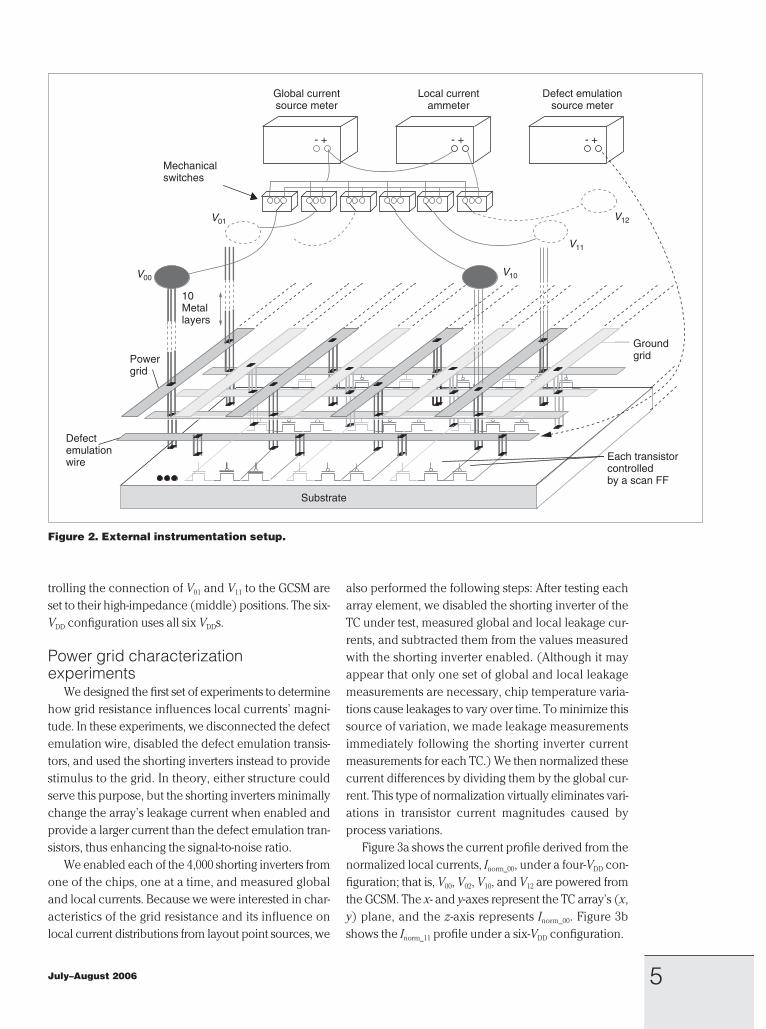
trolling the connection of V01 and V11 to the GCSM are
set to their high-impedance (middle) positions. The six-
VDD configuration uses all six VDDs.
Power grid characterizationexperiments
We designed the first set of experiments to determine
how grid resistance influences local currents’ magni-
tude. In these experiments, we disconnected the defect
emulation wire, disabled the defect emulation transis-
tors, and used the shorting inverters instead to provide
stimulus to the grid. In theory, either structure could
serve this purpose, but the shorting inverters minimally
change the array’s leakage current when enabled and
provide a larger current than the defect emulation tran-
sistors, thus enhancing the signal-to-noise ratio.
We enabled each of the 4,000 shorting inverters from
one of the chips, one at a time, and measured global
and local currents. Because we were interested in char-
acteristics of the grid resistance and its influence on
local current distributions from layout point sources, we
also performed the following steps: After testing each
array element, we disabled the shorting inverter of the
TC under test, measured global and local leakage cur-
rents, and subtracted them from the values measured
with the shorting inverter enabled. (Although it may
appear that only one set of global and local leakage
measurements are necessary, chip temperature varia-
tions cause leakages to vary over time. To minimize this
source of variation, we made leakage measurements
immediately following the shorting inverter current
measurements for each TC.) We then normalized these
current differences by dividing them by the global cur-
rent. This type of normalization virtually eliminates vari-
ations in transistor current magnitudes caused by
process variations.
Figure 3a shows the current profile derived from the
normalized local currents, Inorm_00, under a four-VDD con-
figuration; that is, V00, V02, V10, and V12 are powered from
the GCSM. The x- and y-axes represent the TC array’s (x,
y) plane, and the z-axis represents Inorm_00. Figure 3b
shows the Inorm_11 profile under a six-VDD configuration.
5July–August 2006
Global currentsource meter
Local currentammeter
Defect emulationsource meter
Mechanicalswitches
10Metallayers
Powergrid
Substrate
Each transistorcontrolledby a scan FF
Defectemulationwire
V00
V01
V10
V11
V12
- + - + - +
Groundgrid
Figure 2. External instrumentation setup.
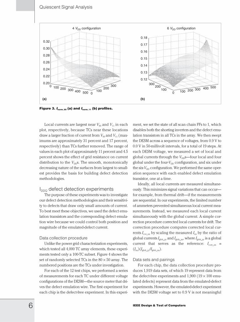
Local currents are largest near V00 and V11 in each
plot, respectively, because TCs near these locations
draw a larger fraction of current from V00 and V11 (max-
imums are approximately 31 percent and 17 percent,
respectively) than TCs further removed. The range of
values in each plot of approximately 11 percent and 4.5
percent shows the effect of grid resistance on current
distribution to the VDDs. The smooth, monotonically
decreasing nature of the surfaces from largest to small-
est provides the basis for building defect detection
methodologies.
IDDQ defect detection experimentsThe purpose of these experiments was to investigate
our defect detection methodologies and their sensitivi-
ty to defects that draw only small amounts of current.
To best meet these objectives, we used the defect emu-
lation transistors and the corresponding defect emula-
tion wire because we could control both position and
magnitude of the emulated-defect current.
Data collection procedureUnlike the power grid characterization experiments,
which tested all 4,000 TC array elements, these experi-
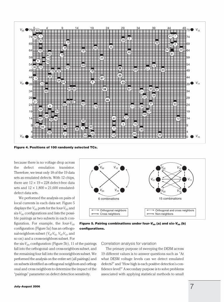
ments tested only a 100-TC subset. Figure 4 shows the
set of randomly selected TCs in the 80 × 50 array. The
numbered positions are the TCs under investigation.
For each of the 12 test chips, we performed a series
of measurements for each TC under different voltage
configurations of the DESM—the source meter that dri-
ves the defect emulation wire. The first experiment for
each chip is the defect-free experiment. In this experi-
ment, we set the state of all scan chain FFs to 1, which
disables both the shorting inverters and the defect emu-
lation transistors in all TCs in the array. We then swept
the DESM across a sequence of voltages, from 0.9 V to
0.0 V in 50-millivolt intervals, for a total of 19 steps. At
each DESM voltage, we measured a set of local and
global currents through the VDDs—four local and four
global under the four-VDD configuration, and six under
the six-VDD configuration. We performed the same oper-
ation sequence with each enabled defect emulation
transistor, one at a time.
Ideally, all local currents are measured simultane-
ously. This minimizes signal variations that can occur—
for example, from thermal drift—if the measurements
are sequential. In our experiments, the limited number
of ammeters prevented simultaneous local current mea-
surements. Instead, we measured each local current
simultaneously with the global current. A simple cor-
rection procedure corrected local currents for drift. The
correction procedure computes corrected local cur-
rents Icor_xx by scaling the measured Ixx by the ratio of
global currents Iglob_yy and Iglob_xx, where Iglob_yy is a global
current that serves as the reference: Icorr_xx =
(Ixx)(Iglob_yy/Iglob_xx).
Data sets and pairingsFor each chip, the data collection procedure pro-
duces 1,919 data sets, of which 19 represent data from
the defect-free experiments and 1,900 (19 × 100 emu-
lated defects) represent data from the emulated-defect
experiments. However, the emulated-defect experiment
with the DESM voltage set to 0.9 V is not meaningful
Quiescent Signal Analysis
6 IEEE Design & Test of Computers
4 VDD configuration 6 VDD configuration
0.32
0.30
0.28
0.26
0.24
0.22
0.20
0.18
0.17
0.16
0.15
0.14
0.13
0.12
0 100 200 300 100200
300
4000
100200
300
0 100 200 300 400 500
500
(a) (b)
Figure 3. Inorm_00 (a) and Inorm_11 (b) profiles.
because there is no voltage drop across
the defect emulation transistor.
Therefore, we treat only 18 of the 19 data
sets as emulated defects. With 12 chips,
there are 12 × 19 = 228 defect-free data
sets and 12 × 1,800 = 21,600 emulated-
defect data sets.
We performed the analysis on pairs of
local currents in each data set. Figure 5
displays the VDD ports for the four-VDD and
six-VDD configurations and lists the possi-
ble pairings as two subsets in each con-
figuration. For example, the four-VDD
configuration (Figure 5a) has an orthogo-
nal-neighbors subset (V00-V02, V00-V10, and
so on) and a cross-neighbors subset. For
the six-VDD configuration (Figure 5b), 11 of the pairings
fall into the orthogonal- and cross-neighbors subset, and
the remaining four fall into the nonneighbors subset. We
performed the analysis on the entire set (all pairings) and
on subsets identified as orthogonal neighbors and orthog-
onal and cross neighbors to determine the impact of the
“pairings” parameter on defect detection sensitivity.
Correlation analysis for variationThe primary purpose of sweeping the DESM across
19 different values is to answer questions such as “At
what DESM voltage levels can we detect emulated
defects?” and “How high is each positive detection’s con-
fidence level?” A secondary purpose is to solve problems
associated with applying statistical methods to small
7July–August 2006
0
12
3
4
5
6
7
89
10
11
12
13
14
16
17
1819
20
21
22
23
24
25
26
27
28
29
30
31
3233
34
35
36
37
38
39
40
41
42
43
44
45
46
4748
49
50
51
52
5354
55
56
57
58
59
6061
62
6364
65
66
6768
69
70
71
72
73
74
75
76
77
78
79
80
81
82
83
84
85
86
87
88
89
90
91
92
93
94
95
96
97
98
99
0 4 9 14 19 24 29 34 39 44 4979
74
69
59
54
64
49
44
39
34
29
24
19
14
9
4
0
79
74
69
59
54
64
49
44
39
34
29
24
19
14
9
4
0
V02
V01
V00
V12
V11
V10
Figure 4. Positions of 100 randomly selected TCs.
V02 V02
V01 V11
V12 V12
V00 V10V10V00
15 combinations6 combinations
Orthogonal neighborsCross neighbors
Orthogonal and cross neighborsNon-neighbors
Figure 5. Pairing combinations under four-VDD (a) and six-VDD (b)
configurations.
data sets—that is, the 12 chips. For this, we used the 19
defect-free data sets obtained from each chip under dif-
ferent DESM voltages to increase the sample size. To
eliminate any concerns that this might unfairly bias the
results, we also give the results of an analysis that used
only one set of defect-free data from each chip.
A third purpose is the analysis of variance in the
data. By using the defect-free data sets obtained from a
single chip, we can decompose several sources of vari-
ation that affect the results, such as variations intro-
duced by test apparatus and power grid parameters. A
comparative analysis using data sets from other chips
lets us identify the relative magnitude and significance
of these variation sources.
Correlation analysis of defect-free data from asingle chip
Perhaps the most challenging aspect of hardware
experiments, in comparison with simulation experi-
ments, is understanding and accounting for various
sources of signal variations. The measured parameter
in our experiments, IDDQ, is analog in nature and is sub-
ject to variations associated with the measurement
instrumentation and test apparatus. These variations
include noise and series parasitic resistances, as well as
variations in the chip itself, such as pin and routing par-
asitics and within-die and between-die process varia-
tions. It is important to understand the relative effect of
these signal variation sources as well as to have a means
of calibrating for them.
In the context of our test methods, the most mean-
ingful approach to decomposing signal variation sources
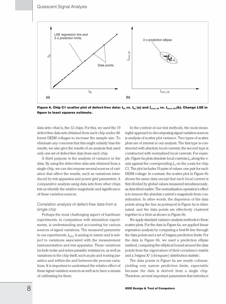
is analysis of scatter plot variance. Two types of scatter
plots are of interest in our analysis. The first type is con-
structed with absolute local currents; the second type is
constructed with normalized local currents. For exam-
ple, Figure 6a plots absolute local currents I00 along the x-
axis against the corresponding I02 on the y-axis for chip
C1. The plot includes 19 pairs of values, one pair for each
DESM voltage. In contrast, the scatter plot in Figure 6b
shows the same data except that each local current is
first divided by global values measured simultaneously,
as described earlier. The normalization operation’s effect
is to remove the absolute current’s magnitude from con-
sideration. In other words, the dispersion of the data
points along the line as portrayed in Figure 6a is elimi-
nated, and the data points are effectively clustered
together in a blob as shown in Figure 6b.
We apply standard variance analysis methods to these
scatter plots. For the data in Figure 6a, we applied linear
regression analysis by computing a best-fit line through
the data points and a set of 3-sigma prediction limits. For
the data in Figure 6b, we used a prediction ellipse
method, computing the elliptical bound around the data
points from the eigenvalues of their covariance matrix
and a 3-sigma Χ2 (chi-square) distribution statistic.
The data points in Figure 6a are nearly colinear,
yielding very narrow prediction limits, expectable
because the data is derived from a single chip.
Therefore, several important parameters that introduce
Quiescent Signal Analysis
8 IEEE Design & Test of Computers
I00 Inorm_00
I 02
I nor
m_0
2
Data points
LSE regression line and3 σ prediction limits
3 σ prediction ellipse
(a) (b)
Figure 6. Chip C1 scatter plot of defect-free data: I00 vs. I02 (a) and Inorm_00 vs. Inorm_02.(b). Change LSE in
figure to least squares estimate.
dispersion of the data points are held constant, such as
series resistance between the power supply and the VDD
ports and on-chip process variation parameters. The
remaining variation sources are environmental changes
such as temperature and noise. We minimize tempera-
ture variations by collecting both data points in each
pair closely together in time as described earlier.
Therefore, most variation is due to noise. The noise floor
in the existing test setup is approximately 300 nA.
We draw similar conclusions from the data dis-
played in Figure 6b, except that the dispersion is more
pronounced. This is due, in part, to the difference in
scaling factors used to plot the data. However, the dis-
persion is actually larger than that present in the scatter
plot in Figure 6a. In this case, the normalization opera-
tion is responsible for increasing the dispersion because
the divisor—the global current measurement—is also
subject to noise. Moreover, the measurement’s global
context—the entire array—is subject to a wider range
of process variations than the regional context associ-
ated with two local measurements. As will become evi-
dent in the defect sensitivity analysis given in the
following sections, these elements can reduce detec-
tion sensitivity of small defect currents.
Correlation analysis of defect-free data frommultiple chips
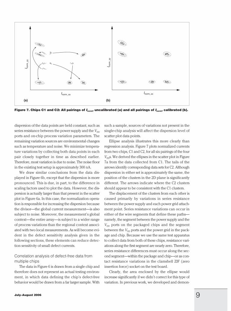
The data in Figure 6 is drawn from a single chip and
therefore does not represent an actual testing environ-
ment, in which data defining the chip’s defect-free
behavior would be drawn from a far larger sample. With
such a sample, sources of variations not present in the
single-chip analysis will affect the dispersion level of
scatter plot data points.
Ellipse analysis illustrates this more clearly than
regression analysis. Figure 7 plots normalized currents
from two chips, C1 and C2, for all six pairings of the four
VDDs. We derived the ellipses in the scatter plot in Figure
7a from the data collected from C1. The tails of the
arrows identify corresponding data sets for C2. Although
dispersion in either set is approximately the same, the
position of the clusters in the 2D plane is significantly
different. The arrows indicate where the C2 clusters
should appear to be consistent with the C1 clusters.
The displacement of the clusters from each other is
caused primarily by variations in series resistance
between the power supply and each power grid attach-
ment point. Series resistance variations can occur in
either of the wire segments that define these paths—
namely, the segment between the power supply and the
VDD ports on the packaged chips and the segment
between the VDD ports and the power grid in the pack-
age and chip. Because we use the same test apparatus
to collect data from both of these chips, resistance vari-
ations along the first segment are nearly zero. Therefore,
series resistance differences must occur along the sec-
ond segment—within the package and chip—or as con-
tact resistance variations in the clamshell ZIF (zero
insertion force) socket on the test board.
Clearly, the area enclosed by the ellipse would
increase significantly if we didn’t correct for this type of
variation. In previous work, we developed and demon-
9July–August 2006
I nor
m_y
y
I nor
m_y
y
Inorm_xxInorm_xx
(a) (b)
Figure 7. Chips C1 and C2: All pairings of Inorm, uncalibrated (a) and all pairings of Inorm, calibrated (b).
strated a probe card calibration (PCC) technique.7 The
method uses data collected from a special set of calibra-
tion circuits similar in design to the TCs shown in Figure
1b, with only the shorting inverters present. For PCC, we
place one copy of the TC underneath each VDD port.
Figure 1a shows the positions of the TCs (TC0,0, TC0,39, and
so on) used for PCC in these experiments. We collect the
data for PCC by enabling the shorting inverter in each TC,
one at a time, and measuring local currents. We also take
leakage measurements as described earlier and subtract
them from the shorting-inverter currents. (Peak values in
Figures 3a and 3b correspond to the shorting-inverter cur-
rents of TC0,0 and TC49,39, respectively. By placing the TCs
at points directly beneath the power ports, we minimize
the signal-to-noise ratio. This choice of position is also
beneficial for diagnostic purposes.8) We normalize the
shorting-inverter currents by dividing them by the global
current, both with leakage subtracted.
We use the data matrix collected in the PCC tests to
calibrate the local currents measured in other tests. We
do this by using the matrices obtained from two chips: a
chip whose data is to be corrected, such as C2, and a ref-
erence chip, such as C1. For each chip, the matrix is 4 ×4 under the four-VDD configuration. Equation 1 gives the
expression for computing the transformation matrix, X:
(1)
Once we obtain X, we calibrate any set of measured
currents from C2, such as the data shown in Figure 7a,
using the linear transformation operator defined by
Equation 2:
(2)
Figure 7b shows the transformation result. The C2
clusters have been linearly displaced to locations cor-
responding to the C1 clusters. We derive prediction
ellipses at 3 sigma using the combined data sets shown
in the figure. The area enclosed by the new ellipses in
Figure 7b is similar to that shown for C1 in Figure 7a.
This is a desirable characteristic because defect detec-
tion sensitivity strongly correlates to the dispersion level
in the defect-free data.
Defect current and background leakage in testchips
An important advantage of measuring local currents
at each supply port is the increased observability this
method provides. Here, observability refers to the abili-
ty to distinguish between current drawn by a defect and
normal background leakage current. For example, if a
chip contains 100 power ports, the leakage current
through any one VDD port will be approximately 100
times smaller, on average, than the leakage current
measured globally. Therefore, measuring local currents
greatly increases the probability of detecting a defect,
particularly in large chips with many VDD ports.
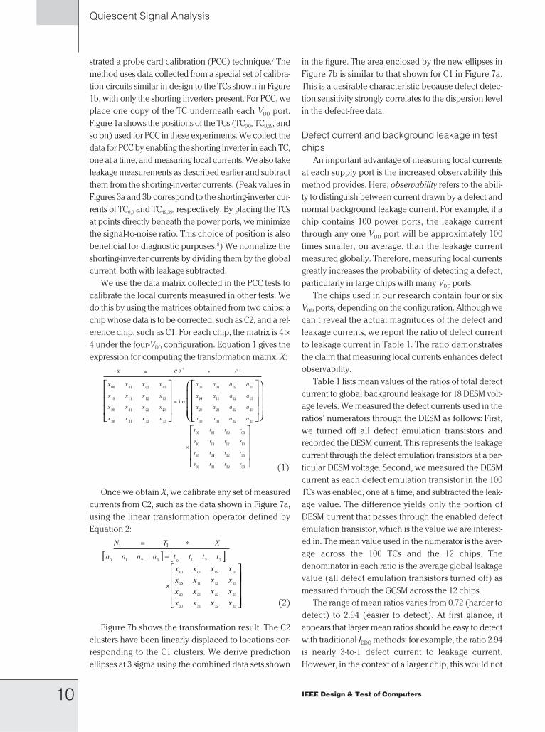
The chips used in our research contain four or six
VDD ports, depending on the configuration. Although we
can’t reveal the actual magnitudes of the defect and
leakage currents, we report the ratio of defect current
to leakage current in Table 1. The ratio demonstrates
the claim that measuring local currents enhances defect
observability.
Table 1 lists mean values of the ratios of total defect
current to global background leakage for 18 DESM volt-
age levels. We measured the defect currents used in the
ratios’ numerators through the DESM as follows: First,
we turned off all defect emulation transistors and
recorded the DESM current. This represents the leakage
current through the defect emulation transistors at a par-
ticular DESM voltage. Second, we measured the DESM
current as each defect emulation transistor in the 100
TCs was enabled, one at a time, and subtracted the leak-
age value. The difference yields only the portion of
DESM current that passes through the enabled defect
emulation transistor, which is the value we are interest-
ed in. The mean value used in the numerator is the aver-
age across the 100 TCs and the 12 chips. The
denominator in each ratio is the average global leakage
value (all defect emulation transistors turned off) as
measured through the GCSM across the 12 chips.
The range of mean ratios varies from 0.72 (harder to
detect) to 2.94 (easier to detect). At first glance, it
appears that larger mean ratios should be easy to detect
with traditional IDDQ methods; for example, the ratio 2.94
is nearly 3-to-1 defect current to leakage current.
However, in the context of a larger chip, this would not
N T X
n n n n t t t t
x x x x
x
1 1
0 1 2 3 0 1 2 3
00 01 02 03
1
= ∗
=
×
[ ] [ ]
00 11 12 13
20 21 22 23
30 31 32 33
x x x
x x x x
x x x x
⎡
⎣
⎢⎢⎢⎢
⎤
⎦
⎥⎥⎥⎥⎥
X
x x x x
x x x x
x x x x
= ∗−
C C2 11
00 01 02 03
10 11 12 13
20 21 22 223
30 31 32 33
00 01 02 03
1
x x x x
a a a a
a
⎡
⎣
⎢⎢⎢
⎤
⎦
⎥⎥⎥
= inv00 11 12 13
20 21 22 23
30 31 32 33
a a a
a a a a
a a a a
⎡
⎣
⎢⎢⎢
⎤
⎦
⎥⎥⎥⎥
⎛
⎝
⎜⎜⎜
⎞
⎠
⎟⎟⎟
×
r r r r
r r r r
r r
00 01 02 03
10 11 12 13
20 211 22 23
30 31 32 33
r r
r r r r
⎡
⎣
⎢⎢⎢
⎤
⎦
⎥⎥⎥
Quiescent Signal Analysis
10 IEEE Design & Test of Computers
be the case. To illustrate this, the third column of Table
1 lists the projected ratios for a chip approximately 1
cm2 in size.
The hypothetical 1-cm2 chip contains 468 copies of
the TC array and contains a 27 × 19 power port area
array. As a conservative estimate, the ratios given in the
second column are scaled in the third column by 468/4
= 117. The factor of 4 provides an allowance for redis-
tribution of defect and leakage current in the larger
array that adversely affects detection sensitivity. (We
chose the value 4 assuming that redistribution causes
defect current to be reduced by half and leakage cur-
rent to double over that measured in a chip with one
copy of the array, as we do here.) Under these assump-
tions, the smallest projected ratio is 0.006, as given in
the first row of the table for the DESM voltage of 0.85.
This indicates that the defect current measured in our
experiments would be more than 160 times smaller than
the leakage current in the hypothetical chip. In specif-
ic cases in our experiments, we could detect defect cur-
rent in ratios smaller than the values shown in the table
by a factor of 4, and we believe this factor could be as
large as 10 with improved signal-to-noise ratios.
Emulated-defect detection resultsThis section presents the results of applying regres-
sion and ellipse analysis to the IDDQ data collected from
12 chips, as we described in the previous section. We
report the detection sensitivity as well as the number of
test escapes and yield loss for several pairing subsets.
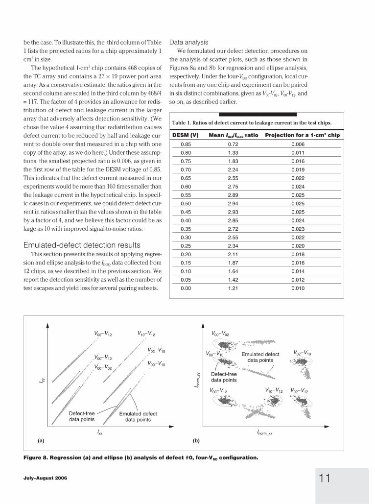
Data analysisWe formulated our defect detection procedures on
the analysis of scatter plots, such as those shown in
Figures 8a and 8b for regression and ellipse analysis,
respectively. Under the four-VDD configuration, local cur-
rents from any one chip and experiment can be paired
in six distinct combinations, given as V00-V02, V00-V12, and
so on, as described earlier.
11July–August 2006
Table 1. Ratios of defect current to leakage current in the test chips.
DESM (V) Mean Idef/Ileak ratio Projection for a 1-cm2 chip
0.85 0.72 0.006
0.80 1.33 0.011
0.75 1.83 0.016
0.70 2.24 0.019
0.65 2.55 0.022
0.60 2.75 0.024
0.55 2.89 0.025
0.50 2.94 0.025
0.45 2.93 0.025
0.40 2.85 0.024
0.35 2.72 0.023
0.30 2.55 0.022
0.25 2.34 0.020
0.20 2.11 0.018
0.15 1.87 0.016
0.10 1.64 0.014
0.05 1.42 0.012
0.00 1.21 0.010
I nor
m_y
y
I yy
Inorm_xx
Defect-freedata points
Emulated defectdata points
Emulated defectdata points
Defect-freedata points
Ixx
V02−V12
V02−V12
V00−V12
V00−V12
V00−V02
V00−V02V10−V12
V10−V12
V02−V10 V02−V10
V00−V10
V00−V10
(a) (b)
Figure 8. Regression (a) and ellipse (b) analysis of defect #0, four-VDD configuration.
We derived the scatter plots shown in Figure 8 from
experiments that investigate defect #0, as shown at posi-
tion (x, y) = (5, 21) in Figure 4. We drew the defect-free
data used to compute the prediction limits in Figure 8a
and the prediction ellipses in Figure 8b from 12 chips at
each of 19 DESM voltages for a total of 228 data points.
The emulated-defect data also comes from the 12 chips
at each of 18 DESM voltages for a total of 216 data
points. (The same defect-free data and limits are used
in the analysis of all 100 emulated defects.)
The scatter plots for each of the six pairings in Figure
8a are offset along the x and y axes to assist the visual
presentation of the data. The prediction limits in Figure
8a are extremely narrow and appear as a single line.
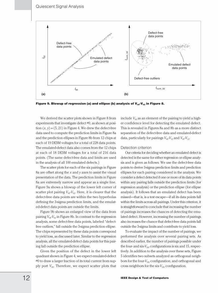
Figure 9a shows a blowup of the lower left corner of
scatter plot pairing V00-V02. Here, it is clearer that the
defect-free data points are within the two hyperbolas
defining the 3-sigma prediction limits, and the emulat-
ed-defect data points are outside the limits.
Figure 9b shows an enlarged view of the data from
pairing V00-V02 in Figure 8b. In contrast to the regression
analysis, some defect-free data points, labeled “defect-
free outliers,” fall outside the 3-sigma prediction ellipse.
The chips represented by these data points correspond
to yield loss, as discussed later. Similar to the regression
analysis, all the emulated-defect data points for this pair-
ing fall outside the prediction ellipse.
Given the position of the defect in the lower left
quadrant shown in Figure 4, we expect emulated-defect
#0 to draw a larger fraction of its total current from sup-
ply port V00. Therefore, we expect scatter plots that
include V00 as an element of the pairing to yield a high-
er confidence level for detecting the emulated defect.
This is revealed in Figures 8a and 8b as a more distinct
separation of the defect-free data and emulated-defect
data, particularly for pairings V00-V10 and V00-V12.
Detection criterionOur criteria for deciding whether an emulated defect is
detected is the same for either regression or ellipse analy-
sis and is given as follows: We use the defect-free data
points to derive 3-sigma prediction limits and prediction
ellipses for each pairing considered in the analysis. We
consider a defect detected if one or more of its data points
within any pairing falls outside the prediction limits (for
regression analysis) or the prediction ellipse (for ellipse
analysis). It follows that an emulated defect has been
missed—that is, is a test escape—if all its data points fall
within the limits across all pairings. Under this criterion, it
is straightforward to conclude that increasing the number
of pairings increases the chances of detecting the emu-
lated defect. However, increasing the number of pairings
also increases the chance that defect-free data points fall
outside the 3-sigma limits and contribute to yield loss.
To evaluate the impact of the number of pairings, we
performed the analysis over several pairing sets. As
described earlier, the number of pairings possible under
the four- and six-VDD configurations is six and 15, respec-
tively. In addition to the analysis over these sets, Figure
5 identifies two subsets analyzed as orthogonal neigh-
bors for the four-VDD configuration, and orthogonal and
cross neighbors for the six-VDD configuration.
Quiescent Signal Analysis
12 IEEE Design & Test of Computers
Defect-freedata points
Inorm_00
I nor
m_0
2
I 02
I00
Defect-freedata points
Emulated defectdata points
Emulated defectdata points
Defect-free outliers
(a) (b)
Figure 9. Blowup of regression (a) and ellipse (b) analysis of V00-V02 in Figure 8.
Test escape and yield loss analysisusing all defect-free data
Our regression and ellipse analysis
used defect-free and emulated-defect data
sets from 12 chips. As discussed, we can
“artificially” increase the sample size of the
defect-free data sets by considering the
tests performed at each of the 19 distinct
DESM voltages as a separate chip. Under
these conditions, the number of defect-
free data sets increases from 12 to 228.
For regression analysis, the inclusion of
the additional data sets improves defect
sensitivity because the wider range of leak-
age currents produced across the different
DESM voltages increases the data point
spread along the x-axis in the scatter plots.
As long as dispersion is small around the
regression line, this characteristic keeps
the prediction limits small along the regres-
sion line’s entire length. Figure 9a, in
which the hyperbola-shaped prediction
limits actually appear straight and parallel
with the regression line, illustrates this characteristic.
In contrast, for ellipse analysis, including the addi-
tional defect-free data sets weakens the method’s defect
sensitivity, particularly when we include data sets asso-
ciated with lower signal-to-noise ratios—those associ-
ated with the larger DESM voltages. This is true because
the dispersion captured by the ellipse is defined by the
worst-case dispersion across the entire range of values
measured. The larger dispersion added by the lower
defect-free currents adversely affects the detection sen-
sitivity of defects that produce larger currents. This does
not happen with regression, because separate limits are
defined and preserved along the x-axis for each current
level in the defect-free data.
Table 2 gives the results of regression and ellipse
analysis using the pairing subsets described in the pre-
vious section under the four- and six-VDD configurations.
The pair of numbers reported in each cell of the table
corresponds to the number of emulated defects that
were not detected (test escapes) and the number of
defect-free chips that failed the test (yield loss), respec-
tively. As indicated previously, we tested 21,600 emu-
lated defects and 228 defect-free chips. The ideal result
is 0/0: no test escapes and no yield loss.
The regression analysis results are clearly superior to
the ellipse analysis results. Overall, regression performs
very well—for example, missing less than 1 percent of
the emulated defects and having less than 1 percent
yield loss under the all-pairings four-VDD configuration.
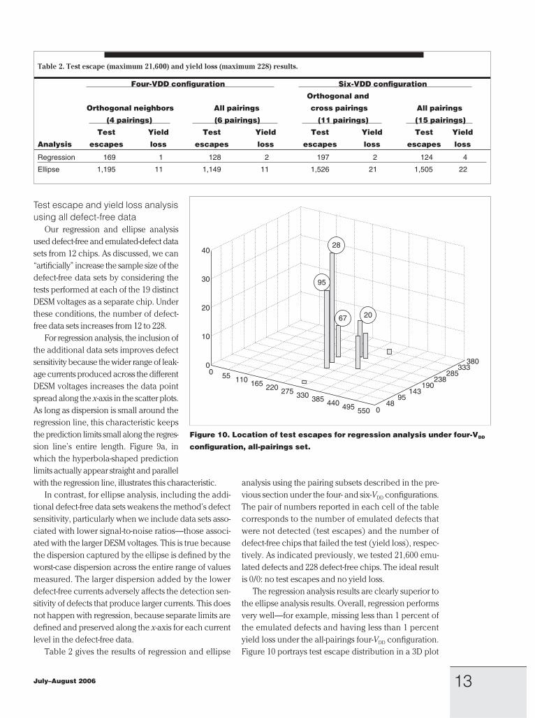
Figure 10 portrays test escape distribution in a 3D plot
13July–August 2006
Table 2. Test escape (maximum 21,600) and yield loss (maximum 228) results.
Four-VDD configuration Six-VDD configuration
Orthogonal and
Orthogonal neighbors All pairings cross pairings All pairings
(4 pairings) (6 pairings) (11 pairings) (15 pairings)
Test Yield Test Yield Test Yield Test Yield
Analysis escapes loss escapes loss escapes loss escapes loss
Regression 169 1 128 2 197 2 124 4
Ellipse 1,195 11 1,149 11 1,526 21 1,505 22
0
0 55 110 165 220 275 330 385 440 495 55048
95143
190238
285333
380
40
30
20
10
0
95
67
28
20
Figure 10. Location of test escapes for regression analysis under four-VDD
configuration, all-pairings set.
in which the (x, y) plane represents the TC array, as
shown in Figure 4. The bar height indicates the number
of times that the emulated defect at that position was
missed. Clearly, the bars are 0 in all cases except for the
emulated defects in the center of the grid. The circled
defect number identifiers (defined in Figure 4) above
four of the bars are the emulated defects most often
missed. (Because each defect is tested at 18 DESM volt-
ages on 12 chips, the maximum z value for any defect
is 216.) Moreover, these are the only defects missed at
DESM voltages smaller than 0.85 V.
All the emulated defects missed under either regres-
sion or ellipse analysis are located in the center of the
power grid. This region distributes the emulated defec-
t’s current almost equally among surrounding VDD ports.
The lack of an anomalous local current variation can-
not be distinguished from global changes in back-
ground leakage current. However, in larger chips that
incorporate more VDD ports, the center portion of this
grid would be asymmetric to VDD ports outside this
region. Therefore, the defects missed here may be
detectable in pairings involving VDDs outside this region
in larger grids. We are currently conducting experi-
ments that apply power to other subsets of VDD ports (for
example, V01, V02, and V12) to determine whether it is
possible to detect the defects missed under the four-
and six-VDD configurations investigated here.
The results shown in Table 2 for regression under the
four- and six-VDD configurations don’t suggest that one
is significantly better than the other. For example, the
number of test escapes and yield loss are 128 and 2 ver-
sus 124 and 4, respectively. In contrast, the differences
are more significant for ellipse analysis, with 1,149 and
11 versus 1,505 and 22. As discussed earlier, the noise
in global currents adversely affects ellipse analysis. The
noise effect is more pronounced under the six-VDD con-
figuration because local currents are smaller and closer
to the noise floor than currents measured under the
four-VDD configuration.
It is clear under either analysis that larger subsets of
pairings reduce the number of test escapes at the
expense of increasing yield loss. For example, under the
regression results in the second and third columns in
Table 2, test escapes decrease from 169 for the orthog-
onal-neighbors subset to 128 for the all-pairings set, and
yield loss increases correspondingly from 1 to 2. (Note
that for the subsets in columns two and four, the num-
ber of test escapes can never be smaller and the yield
loss can never be larger than the all-pairings set,
because the latter includes the subset pairings in its
analysis.) Given the detection criteria, we expect a
decrease in test escapes as more pairings are included
in the analysis. The yield loss increase is caused by the
larger magnitude of within-chip process variations in
pairings more widely separated in the layout. The cross-
correlation profile of defect-free data from nonneigh-
boring VDD ports has a higher dispersion level, which
increases the chance that defect-free data points will
become outliers.
Test escape and yield loss analysis using asubset of defect-free data
The analysis given in the preceding subsection indi-
cates that regression analysis is superior in terms of
reducing test escapes and yield loss. However, ellipse
analysis performed under a special condition produces
the best overall result with 71 test escapes and no yield
loss. The special condition involves restricting the
defect-free samples used to derive the prediction
ellipses to those collected with the highest background
leakage—that is, with the DESM voltage set to 0.0 V.
Although this constraint is difficult to realize in produc-
tion testing, it demonstrates an important advantage of
ellipse analysis over regression for situations in which
we can obtain good signal-to-noise ratios.
The discussion of Figure 9a indicated that the hyper-
bola prediction limits appear as straight lines because
the distribution of defect-free currents is large. The dis-
tribution of the 228 data points along the x-axis keeps
the prediction limits close to the regression line’s entire
length. If this did not hold true—if the distribution of
defect-free data were clustered in a small region along
the x-axis—the curves’ hyperbolic nature would be far
more pronounced, and the prediction limits would
widen significantly around the regression line on either
side of the cluster. This would reduce the method’s sen-
sitivity for emulated defects that produce data points on
either side of the cluster. Therefore, regression works
well in our experiments because the sum of the emu-
lated-defect and leakage currents is of the same order
as the leakage currents alone.
As discussed earlier, ellipse analysis is more sensi-
tive to noise than regression because both the local and
global current measurements that define the data
point’s position possess a noise element. Under the
assumption that the noise floor is independent of the
current’s magnitude, it follows that the adverse impact
of noise is smaller for larger-magnitude currents.
Therefore, prediction ellipses derived using larger
defect-free currents will be smaller.
Quiescent Signal Analysis
14 IEEE Design & Test of Computers
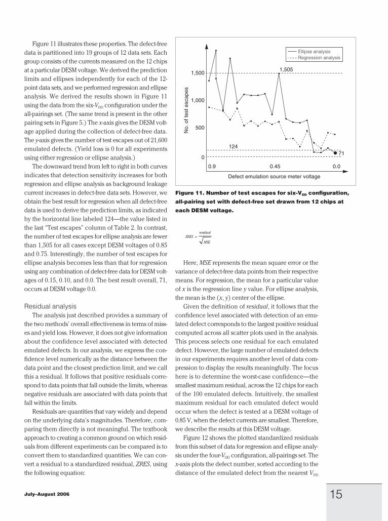
Figure 11 illustrates these properties. The defect-free
data is partitioned into 19 groups of 12 data sets. Each
group consists of the currents measured on the 12 chips
at a particular DESM voltage. We derived the prediction
limits and ellipses independently for each of the 12-
point data sets, and we performed regression and ellipse
analysis. We derived the results shown in Figure 11
using the data from the six-VDD configuration under the
all-pairings set. (The same trend is present in the other
pairing sets in Figure 5.) The x-axis gives the DESM volt-
age applied during the collection of defect-free data.
The y-axis gives the number of test escapes out of 21,600
emulated defects. (Yield loss is 0 for all experiments
using either regression or ellipse analysis.)
The downward trend from left to right in both curves
indicates that detection sensitivity increases for both
regression and ellipse analysis as background leakage
current increases in defect-free data sets. However, we
obtain the best result for regression when all defect-free
data is used to derive the prediction limits, as indicated
by the horizontal line labeled 124—the value listed in
the last “Test escapes” column of Table 2. In contrast,
the number of test escapes for ellipse analysis are fewer
than 1,505 for all cases except DESM voltages of 0.85
and 0.75. Interestingly, the number of test escapes for
ellipse analysis becomes less than that for regression
using any combination of defect-free data for DESM volt-
ages of 0.15, 0.10, and 0.0. The best result overall, 71,
occurs at DESM voltage 0.0.
Residual analysisThe analysis just described provides a summary of
the two methods’ overall effectiveness in terms of miss-
es and yield loss. However, it does not give information
about the confidence level associated with detected
emulated defects. In our analysis, we express the con-
fidence level numerically as the distance between the
data point and the closest prediction limit, and we call
this a residual. It follows that positive residuals corre-
spond to data points that fall outside the limits, whereas
negative residuals are associated with data points that
fall within the limits.
Residuals are quantities that vary widely and depend
on the underlying data’s magnitudes. Therefore, com-
paring them directly is not meaningful. The textbook
approach to creating a common ground on which resid-
uals from different experiments can be compared is to
convert them to standardized quantities. We can con-
vert a residual to a standardized residual, ZRES, using
the following equation:
Here, MSE represents the mean square error or the
variance of defect-free data points from their respective
means. For regression, the mean for a particular value
of x is the regression line y value. For ellipse analysis,
the mean is the (x, y) center of the ellipse.
Given the definition of residual, it follows that the
confidence level associated with detection of an emu-
lated defect corresponds to the largest positive residual
computed across all scatter plots used in the analysis.
This process selects one residual for each emulated
defect. However, the large number of emulated defects
in our experiments requires another level of data com-
pression to display the results meaningfully. The focus
here is to determine the worst-case confidence—the
smallest maximum residual, across the 12 chips for each
of the 100 emulated defects. Intuitively, the smallest
maximum residual for each emulated defect would
occur when the defect is tested at a DESM voltage of
0.85 V, when the defect currents are smallest. Therefore,
we describe the results at this DESM voltage.
Figure 12 shows the plotted standardized residuals
from this subset of data for regression and ellipse analy-
sis under the four-VDD configuration, all-pairings set. The
x-axis plots the defect number, sorted according to the
distance of the emulated defect from the nearest VDD
ZRES
residual
MSE
=
15July–August 2006
1,500
1,000
500
0
No.
of t
est e
scap
es
Defect emulation source meter voltage
0.9 0.45 0.0
12471
1,505
Ellipse analysisRegression analysis
Figure 11. Number of test escapes for six-VDD configuration,
all-pairing set with defect-free set drawn from 12 chips at
each DESM voltage.
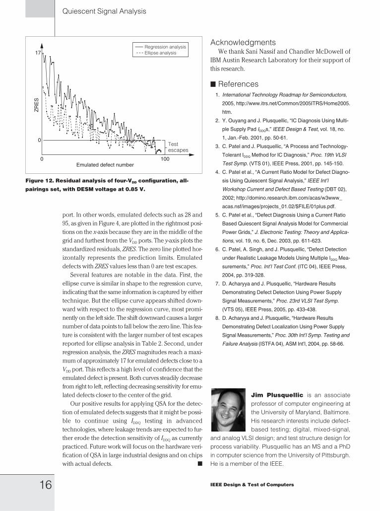
port. In other words, emulated defects such as 28 and
95, as given in Figure 4, are plotted in the rightmost posi-
tions on the x-axis because they are in the middle of the
grid and furthest from the VDD ports. The y-axis plots the
standardized residuals, ZRES. The zero line plotted hor-
izontally represents the prediction limits. Emulated
defects with ZRES values less than 0 are test escapes.
Several features are notable in the data. First, the
ellipse curve is similar in shape to the regression curve,
indicating that the same information is captured by either
technique. But the ellipse curve appears shifted down-
ward with respect to the regression curve, most promi-
nently on the left side. The shift downward causes a larger
number of data points to fall below the zero line. This fea-
ture is consistent with the larger number of test escapes
reported for ellipse analysis in Table 2. Second, under
regression analysis, the ZRES magnitudes reach a maxi-
mum of approximately 17 for emulated defects close to a
VDD port. This reflects a high level of confidence that the
emulated defect is present. Both curves steadily decrease
from right to left, reflecting decreasing sensitivity for emu-
lated defects closer to the center of the grid.
Our positive results for applying QSA for the detec-
tion of emulated defects suggests that it might be possi-
ble to continue using IDDQ testing in advanced
technologies, where leakage trends are expected to fur-
ther erode the detection sensitivity of IDDQ as currently
practiced. Future work will focus on the hardware veri-
fication of QSA in large industrial designs and on chips
with actual defects. ■
AcknowledgmentsWe thank Sani Nassif and Chandler McDowell of
IBM Austin Research Laboratory for their support of
this research.
References1. International Technology Roadmap for Semiconductors,
2005, http://www.itrs.net/Common/2005ITRS/Home2005.
htm.
2. Y. Ouyang and J. Plusquellic, “IC Diagnosis Using Multi-
ple Supply Pad IDDQs,” IEEE Design & Test, vol. 18, no.
1, Jan.-Feb. 2001, pp. 50-61.
3. C. Patel and J. Plusquellic, “A Process and Technology-
Tolerant IDDQ Method for IC Diagnosis,” Proc. 19th VLSI
Test Symp. (VTS 01), IEEE Press, 2001, pp. 145-150.
4. C. Patel et al., “A Current Ratio Model for Defect Diagno-
sis Using Quiescent Signal Analysis,” IEEE Int’l
Workshop Current and Defect Based Testing (DBT 02),
2002; http://domino.research.ibm.com/acas/w3www_
acas.nsf/images/projects_01.02/$FILE/01plus.pdf.
5. C. Patel et al., “Defect Diagnosis Using a Current Ratio
Based Quiescent Signal Analysis Model for Commercial
Power Grids,” J. Electronic Testing: Theory and Applica-
tions, vol. 19, no. 6, Dec. 2003, pp. 611-623.
6. C. Patel, A. Singh, and J. Plusquellic, “Defect Detection
under Realistic Leakage Models Using Multiple IDDQ Mea-
surements,” Proc. Int’l Test Conf. (ITC 04), IEEE Press,
2004, pp. 319-328.
7. D. Acharyya and J. Plusquellic, “Hardware Results
Demonstrating Defect Detection Using Power Supply
Signal Measurements,” Proc. 23rd VLSI Test Symp.
(VTS 05), IEEE Press, 2005, pp. 433-438.
8. D. Acharyya and J. Plusquellic, “Hardware Results
Demonstrating Defect Localization Using Power Supply
Signal Measurements,” Proc. 30th Int’l Symp. Testing and
Failure Analysis (ISTFA 04), ASM Int’l, 2004, pp. 58-66.
Jim Plusquellic is an associateprofessor of computer engineering atthe University of Maryland, Baltimore.His research interests include defect-based testing; digital, mixed-signal,
and analog VLSI design; and test structure design forprocess variability. Plusquellic has an MS and a PhDin computer science from the University of Pittsburgh.He is a member of the IEEE.
Quiescent Signal Analysis
16 IEEE Design & Test of Computers
Emulated defect number
ZR
ES
17
100
Regression analysisEllipse analysis
Testescapes
0
0
Figure 12. Residual analysis of four-VDD configuration, all-
pairings set, with DESM voltage at 0.85 V.
Dhruva Acharyya is an intern atIBM Austin Research Labs and a PhDcandidate at the University of Mary-land, Baltimore. His research interestsinclude power supply testing and test
structure design for measuring process variability.Acharyya has a MS in computer engineering the Uni-versity of Maryland, Baltimore. He is a member of IEEE.
Abhishek Singh is a test engineer atnVidia. His research interests includepower supply testing and fault simula-tion techniques. Abhishek has a PhD incomputer engineering from the Uni-
versity of Maryland, Baltimore. He is a member of IEEE.
Mohammad Tehranipoor is anassistant professor of electrical andcomputer engineering at the Universityof Maryland, Baltimore. His researchinterests include CAD and test for
CMOS VLSI designs and emerging nanoscale devices.Tehranipoor has a PhD in electrical engineering fromthe University of Texas at Dallas. He is a member of theIEEE Computer Society, the ACM, and ACM SIGDA.
Chintan Patel is a research assis-tant professor at the University of Mary-land, Baltimore. His research interestsinclude power supply testing andpower supply monitor design. Chintan
has a PhD in computer engineering from the Universi-ty of Maryland, Baltimore. He is a member of IEEE.
Direct questions and comments about this articleto Jim Plusquellic, Dept. of CSEE, Univ. of Maryland,Baltimore, MD 21250; [email protected].
For further information on this or any other computing
topic, visit our Digital Library at http://www.computer.
org/publications/dlib.
17July–August 2006
Related Documents