Quantum dots: concept and application for image sensors Adri´ an Romero Campelo SUPERVISORS Jorge Fern´ andez Berni Juan Antonio Le˜ nero Bardallo Bachelor’s Thesis Degree in Physics Department of Electronics and Electromagnetism Faculty of Physics Universidad de Sevilla June 2021

Welcome message from author
This document is posted to help you gain knowledge. Please leave a comment to let me know what you think about it! Share it to your friends and learn new things together.
Transcript

Quantum dots: concept andapplication for image sensors
Adrian Romero Campelo
SUPERVISORS
Jorge Fernandez Berni
Juan Antonio Lenero Bardallo
Bachelor’s Thesis
Degree in Physics
Department of Electronics and Electromagnetism
Faculty of Physics
Universidad de Sevilla
June 2021
Abstract
The aim of this Bachelor’s Thesis is to introduce the concept of quantum dots and their
possible application to photodetection. In the first part of this work (Chapter 2), a general
outline of what quantum dots are and how they are manufactured (materials, techniques
employed) will be provided. Besides, a complete description of the band structure of
quantum dots, with an emphasis on their optoelectronic features, will be given too. In
the second part of the thesis (Chapter 3), photodetection technologies are covered. After
an introduction to the state of art of image sensors, the latest advances in quantum dot
photodetection will be presented, considering their figures of merit and possible adaptation
to current available production methods.
i
Contents
List of Figures iv
1 Introduction 1
2 Quantum Dots 3
2.1 Epitaxial crystal growth . . . . . . . . . . . . . . . . . . . . . . . . . . . . 3
2.2 Strained Heterostructures . . . . . . . . . . . . . . . . . . . . . . . . . . . 4
2.2.1 Self-assembled Structures . . . . . . . . . . . . . . . . . . . . . . . . 5
2.3 Colloidal Quantum Dots . . . . . . . . . . . . . . . . . . . . . . . . . . . . 7
2.3.1 Ink-printed QDs . . . . . . . . . . . . . . . . . . . . . . . . . . . . . 7
2.3.2 Spin-coating . . . . . . . . . . . . . . . . . . . . . . . . . . . . . . . 9
2.4 Energy Spectrum of QDs . . . . . . . . . . . . . . . . . . . . . . . . . . . . 10
2.4.1 QD Band structure . . . . . . . . . . . . . . . . . . . . . . . . . . . 10
2.4.2 Effects of strain . . . . . . . . . . . . . . . . . . . . . . . . . . . . . 12
2.4.3 Effects of piezoelectricity . . . . . . . . . . . . . . . . . . . . . . . . 14
2.4.4 Coulomb interaction . . . . . . . . . . . . . . . . . . . . . . . . . . 16
2.4.5 Optical Properties . . . . . . . . . . . . . . . . . . . . . . . . . . . 17
2.4.6 Mini-band formation . . . . . . . . . . . . . . . . . . . . . . . . . . 19
2.5 Simulations . . . . . . . . . . . . . . . . . . . . . . . . . . . . . . . . . . . 20
3 Photodetectors 25
3.1 State of the Art . . . . . . . . . . . . . . . . . . . . . . . . . . . . . . . . . 25
3.1.1 Visible Spectrum . . . . . . . . . . . . . . . . . . . . . . . . . . . . 25
3.1.2 Infrared spectrum . . . . . . . . . . . . . . . . . . . . . . . . . . . . 28
3.2 QD Photodetectors . . . . . . . . . . . . . . . . . . . . . . . . . . . . . . . 31
3.2.1 PbS Quantum Dot Photodetectors . . . . . . . . . . . . . . . . . . 32
ii

3.2.2 Ge Quantum Dot Photodetectors . . . . . . . . . . . . . . . . . . . 41
4 Conclusions 44
A Image Sensor Parameters 51
B Image Sensor Technologies 53
B.0.1 Charge Coupled Devices (CCDs) . . . . . . . . . . . . . . . . . . . 53
B.0.2 Complementary-Metal-Oxide-Semiconductor (CMOS) . . . . . . . . 53
iii
List of Figures
2.1 Types of bonding between substrate and overlayer [37]. . . . . . . . . . . . 4
2.2 Nucleation process of Ge quantum dots grown in Si3N4 [39]. . . . . . . . . 6
2.3 Quantum dots of different sizes, starting at 13 nm up to 90 nm [39]. . . . . 7
2.4 QD printing process: a nozzle releases droplets containing CQD and deposited
on a layer [35]. . . . . . . . . . . . . . . . . . . . . . . . . . . . . . . . . . 8
2.5 Microscope and AFM analysis of a printed QD using as ligands a) NMP,
b) BTA:NMP, c) BTA:NMP on a substrate heated at 60◦C. the latest one
shows the most uniform results and smallest roughness [35]. . . . . . . . . 8
2.6 Process involved in spin coating, including: deposition, spin-up, spin-off
and evaporation [31]. . . . . . . . . . . . . . . . . . . . . . . . . . . . . . . 9
2.7 Energy diagram comparison between the cases without/with strain included
in the model. A: xAs = 0.2, yAs = 0.2; B: xAs = 0.8, yAs = 0.8; C:
xAs = 0.8, yAs = 0.8; A: xAs = 0.2, yAs = 0.8. A notable shift in the
levels can be observed [16]. . . . . . . . . . . . . . . . . . . . . . . . . . . . 15
2.8 Absorption coefficient for a InAs/GaAs QD with base width 124A and
height 62A.The plane polarization is absorbed much more efficiently than
the z-polarization [12]. . . . . . . . . . . . . . . . . . . . . . . . . . . . . . 18
2.9 a) Mini-band as a function of the interdot distance. b) Mini-band as a
function of size (for H=15nm) [21]. . . . . . . . . . . . . . . . . . . . . . . 19
2.10 Quantum Dot Lab interface. . . . . . . . . . . . . . . . . . . . . . . . . . . 20
2.11 Absorption spectrum of the Ge QDs (I). . . . . . . . . . . . . . . . . . . . 21
2.12 Comparison of the absorption spectra for different polarization angles (I). . 22
2.13 Energy states (II). . . . . . . . . . . . . . . . . . . . . . . . . . . . . . . . 23
2.14 Absorption spectrum of the Ge QDs (II). . . . . . . . . . . . . . . . . . . . 23
2.15 Comparison of the absorption spectra for different polarization angles (II). 24
iv

3.1 Simplified diagram showing the absorption and emission processes in a
semiconductor [27]. . . . . . . . . . . . . . . . . . . . . . . . . . . . . . . . 26
3.2 Diagram of an standard silicon photodiode [18]. . . . . . . . . . . . . . . . 27
3.3 Cross section of a photogate [18]. . . . . . . . . . . . . . . . . . . . . . . . 27
3.4 CMOS image sensor, layer by layer [18]. . . . . . . . . . . . . . . . . . . . 28
3.5 Current IR spectrum and its imaging standard ranges [36]. . . . . . . . . . 29
3.6 Cross section of a typical IR sensor [28]. . . . . . . . . . . . . . . . . . . . 30
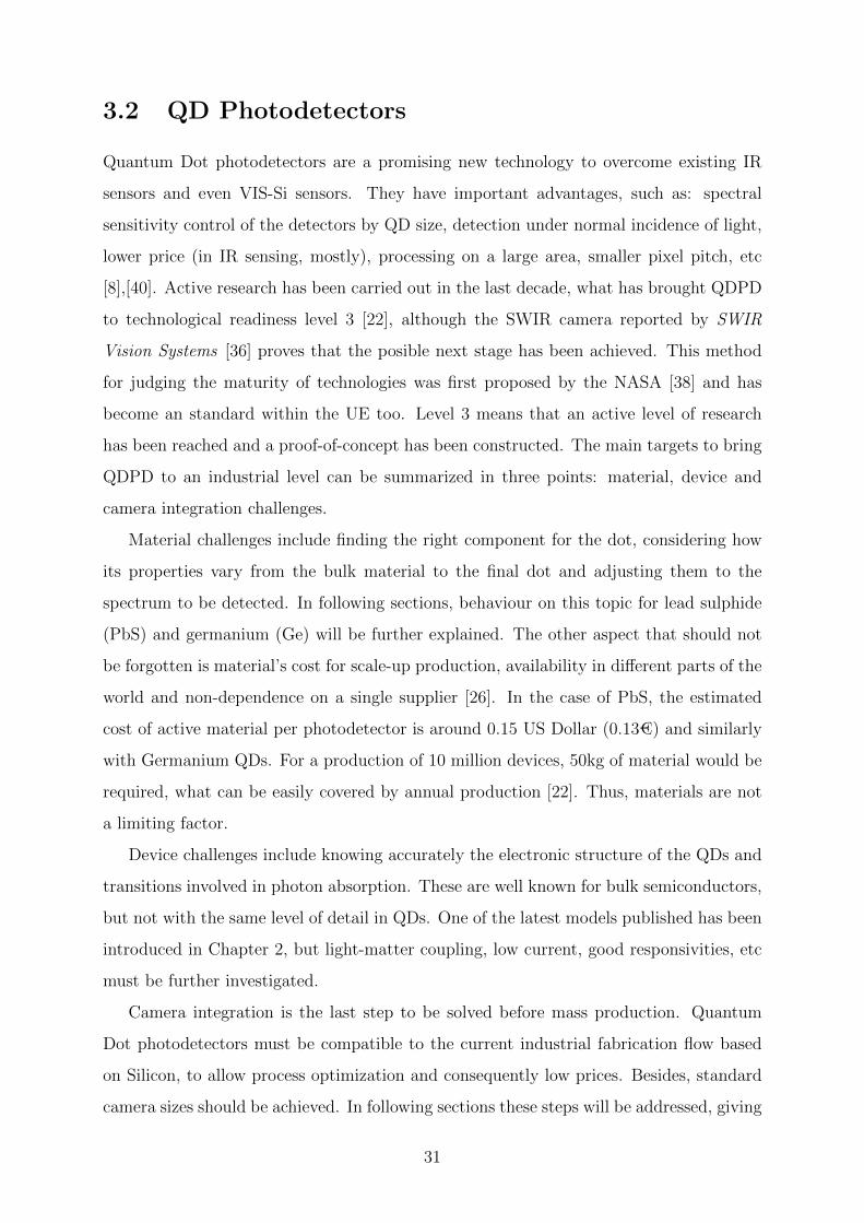
3.7 Schematic comparison of EQE between silicon, InGaAs and PbS QDs [23]. 32
3.8 Absorption peak depending on dot size [23]. . . . . . . . . . . . . . . . . . 33
3.9 Cross image of the QD stack, obtained using annular bright field scanning
transmission electron microscopy [8]. . . . . . . . . . . . . . . . . . . . . . 34
3.10 Cross view of the stack, schematic (left) and obtained by transmission
electron microscopy [23]. . . . . . . . . . . . . . . . . . . . . . . . . . . . . 34
3.11 Photodetector with circuit diagram, includind the TMDC layer [26]. . . . . 34
3.12 Scanning electron microscopy representing the full QD stack [35]. . . . . . 35
3.13 EQE comparison for different bias voltages and wavelengths [35]. . . . . . . 36
3.14 Transient photoresponse [23]. . . . . . . . . . . . . . . . . . . . . . . . . . 37
3.15 Transient photoresponse [8]. . . . . . . . . . . . . . . . . . . . . . . . . . . 37
3.16 Relaxation times [26]. . . . . . . . . . . . . . . . . . . . . . . . . . . . . . . 37
3.17 Deposition of QD layer [10]. . . . . . . . . . . . . . . . . . . . . . . . . . . 38
3.18 QDs islands obtained with photolithography techniques [10]. . . . . . . . . 38
3.19 Packaging of the sensor (left) and cross-section scheme of the photodetector
(right) [8]. . . . . . . . . . . . . . . . . . . . . . . . . . . . . . . . . . . . . 39
3.20 Responsivity comparison of three configurations of QD detectors (left) and
diagram of the dual stack multispectral QDPD (right) [17]. . . . . . . . . . 40
3.21 Schematic figure of a hybrid multispectral sensor, composed by a Si pixel
and a QDPD [8]. . . . . . . . . . . . . . . . . . . . . . . . . . . . . . . . . 40
3.22 Schematic view of a Ge QDPD on a silicon substrate [5]. . . . . . . . . . . 42
3.23 Schematic view of a Ge QDPD on a silicon substrate [32]. . . . . . . . . . . 42
3.24 Responsivity and IQE depending on the wavelength . . . . . . . . . . . . . 43
4.1 Image through a maritime rain event. Picture taken with the Acuros CQD
640/640L GigE SWIR Camera [36]. . . . . . . . . . . . . . . . . . . . . . . 45
v

4.2 Pharmaceutical via labels. Picture taken with the Acuros CQD 640/640L
GigE SWIR Camera [36]. . . . . . . . . . . . . . . . . . . . . . . . . . . . 45
B.1 Diagram of CCD image sensor [18]. . . . . . . . . . . . . . . . . . . . . . . 54
B.2 Potential profile, ilustrating the action of the transfer gate (TG) [7]. . . . . 54
vi
Acronyms
CCD Charge Coupled Device.
CMOS Complementary Metal Oxide Semiconductor.
CQD Colloidal Quantum Dots.
EQE External Quantum Efficiency.
IQE Internal Quantum Efficiency.
ITO Indium Tin Oxide.
LWIR Long Wave Infrared.
MBE Molecular Beam Epitaxy.
MOCVD Metal Organic Chemical Vapor Deposition.
MWIR Medium Wave Infrared.
NIR Near-Infrared.
QD Quantum Dot.
QDPD Quantum Dot Photodetector.
QDs Quantum Dots.
SWIR Short Wave Infrared.
TMDC Transition Metal Dichalcogenide.
vii

Chapter 1
Introduction
Obtaining fixed and lasting pictures has been a major concern since the dawn of the
earliest civilizations, beginning with pictorial techniques and advancing towards more
sophisticated methods. The great steps forward in the field of treatment of the light (e.g.,
the dark chamber) brought the wish of, not only to interpret, but also to reliably capture
what the eye was able to see, and store it permanently. As a result, in the 19th century
the first photographs (and cameras, therefore) were taken, as well as their predecessors,
heliography and daguerreotype. The technological breakthrough behind both was based
in the use of chemical substances, namely silver nitrate or silver chloride, to capture the
image formed by a set of lenses. More accurate and cheaper techniques were developed,
but always based in analogue processes. The next revolution on this field would arrive
with the advent of solid-state image sensors, which appeared parallel to the development
of electronics in the second half of the 20th century.
The era of digital photography also brought a well known term nowadays, the pixel.
Without going into much detail, they are the constituent parts or tiles a picture can
be split up to. Each of these pixels are, in fact, the sensors that react and interpret
the incoming light. The two most common underlying technologies of image sensors are
the Charge Coupled Device (CCD), and the Complementary Metal Oxide Semiconductor
(CMOS) (see Appendix B for more information).
The use of CCDs prevailed over CMOSs, due to their higher performance, specially its
clearly lower Fixed Pattern Noise (FPN), defined as ”the spacial variation of the sensor
response to a uniform input after all the temporal noise has been removed” [18]
1
CMOS sensors were a hot research topic throughout the last decades of the 20th
century, but they would only displace CCDs with the advent of the smartphones, and the
strict size and cost requirements for their cameras. Nowadays, CMOSs sensors are the
benchmark for image sensing, and can be found in smartphone’s cameras, surveillance
systems, professional cameras, etc. It is estimated that their share in the sensors market
sales is of 89%, what makes its economic interest unquestionable [11]. Besides, a compound
annual growth rate of 5.7% in their demand is expected until 2025 [6].
In this search of better and cheaper technologies we find the Quantum Dots (QDs).
On a first approach, they consist in nanometric structures, with electric and optical
properties of a 0-dimension body. One of these features, that makes them interesting
for photodetection, is their absorption and emission tunability to almost any wavelength,
achieving a very precise the identification of the incident light. The opposite effect,
emission, has already become mainstream in the manufacture of televisions, with outstan-
ding results [29].
Although CMOSs sensors have achieved a remarkable performance, they still struggle
in extreme situations, such as excessive or very low light scenes. To overcome these
limitations and others that will be presented in Chapter 3, QD technologies are being
developed by many research groups [26][22][8]. Particularly, QD-based photodetection for
low-light scenes is one of the hottest research topic of these devices, since they’ve shown
great results in the infrared range 1.
The first part of this Bachelor’s Thesis is devoted to provide a complete physical
description of QDs, including electronic and optical characteristic, as well as how they
are manufactured. Simulations of the theoretical properties explained will be presented.
In the second part, current state of the art of CMOSs sensors and how QDs can be
implemented for photodetection will be covered in detail.
1A IR QD based camera has been already commercialized by SWIR Vision Systems
2

Chapter 2
Quantum Dots
Quantum Dots are crystalline structures of nanometric size, with properties changing from
those of the bulk crystal, mainly the density of states (0-D instead of 3-D) and electronic
states. Next sections will provide a description of QDs’ state of the art, covering both
how they are grown and their optoelectronic properties. An accurate description of QDs’
features is fundamental to implement them in new technologies, so this chapter will be
the basis to understand the implementation of a Quantum Dot Photodetector (QDPD)
in Chapter 3.
2.1 Epitaxial crystal growth
The first step in the manufacturing of any active device is to grow the bulk crystal,
that will be used as substrate of the next layers. This is achieved in standard industrial
processes with the Czochralski Technique (CZ), which allows to produce high quality
polycrystalline materials for semiconductors such as Si, GaAs and InP [34]. Once the
bulk crystal is grown, wafers around 250 µm are sliced 1, polished and used for growth of
epitaxial layers.
The two main epitaxial growth techniques are Molecular Beam Epitaxy (MBE) and
Metal Organic Chemical Vapor Deposition (MOCVD). A detailed explanation of both
processes can be found in [34].
1The thickness of the wafers may vary depending on their use, from 250 µm up to 675 µm [33].
3

Figure 2.1: Types of bonding between substrate and overlayer [37].
2.2 Strained Heterostructures
To achieve carrier confinement inside the dot, in general a smaller bandgap material has
to be embedded within a larger bandgap material, although different configurations are
possible. This causes a problem of lattice mismatch between different materials, which
can be, however, overcome or even used in favour of the optoelectronic performance.
In epitaxial processes, the overlayer grown on the substrate can have different lattice
constants; such epitaxy is called strained epitaxy. If the overlayer is very thin, it has
built-in strain and hence the optoelectronic properties are affected. If the substrate and
overlayer lattice constants are respectively as, al, the strain is defined as:
ε =as − alal
(2.1)
Eq.(2.1) gives a value of the mismatch between two materials. It is simple to check
that after 1/ε bonds either a missing or extra bond appears: such defects are called
dislocations. They are named incoherent structures, and they cost energy to the system.
There is another way for the system to rearrange its bonds, namely a coherent structure.
In such cases, substrate and overlayer are almost perfectly bonded by adjusting the lattice
constants, causing the overlayer to be under strain. Thus, the system now has a certain
strain energy and the band diagram of the semiconductor is altered (see Fig. 2.1). For
small lattice mismatch (ε < 0.1), overlayer and substrate fit perfectly. However, as the
thickness of the overlayer increases, dislocations will eventually be favorable in terms of
energy. For example, a surface thickness of as = 10 nm was reported to yield the lowest
dislocation density, for an InAs/GaAsSb system [15].
4
2.2.1 Self-assembled Structures
Strain energy competes against the chemical bonding energy created by bond formation,
as well as the surface effects and the ability of the system to evolve to the minimum free
energy. Self-assembled structures have been reported for a wide variety of semiconductor
pairs, namely Si/Ge, InAs/GaAs, CdSe/ZnSe, InGaN/GaN, (InGa)(AsSb)/GaAs/GaP,
etc [16][3].The main factors affecting the growth are the substrate and deposited material
free energies (γ1, γ2 respectively) and the interface energy γ12. The material’s free energy
is defined as the amount of internal energy available to perform work on the system (the
formation of the structure in this case) [2]. Strain energy of the film µ2(t) should also
be considered,that is, the total amount of energy stored in the formation of the strained
structure. In terms of the lattice mismatch and the free energy, three possible growing
modes may occur:
1. Frank-van der Merwe growth: it is characterized by a low strain (ε < 2%), which
results in an almost perfect growth of layer without dislocations. They show no
strain energy profile. For this case, γ1 > γ2 + γ12.
2. Stranski-Krastonow growth: for intermediate strain values, growth starts with mono-
layers ‘wetting’ the surface but changes to 3D island-growth mode, maintaining the
coherent structure. Thanks to this process, the total free energy of the system is
minimized, and the inequality γ1 > γ2 +γ12 +µ2(tc) is fulfilled (tc critical thickness).
3. Volmer-Weber growth: occurs at higher lattice mismatch. In this case, only island
growth takes place since the cohesive force between atoms in the overlayer is stronger
than the force binding them to the substrate. In this case, γ1 < γ2 + γ12.
Strain provides a mechanism for island-growth, but does not ensure the regular distribution
of the QDs; temperature, flux and total coverage must also be considered. Strain-induced
elastic forces are long-range interactions, meaning that QDs interact strongly among them,
favouring the ”self-organization” [3].
Fabrication of Ge QDs
Any QD growing technique pretending to achieve mass production must first be scalable,
precise and repeatable. Current CMOS fabrication technologies can fulfil those three
5

Figure 2.2: Nucleation process of Ge quantum dots grown in Si3N4 [39].
requirements, so any new device should preferably adapt to them.A compatible fab process
has been recently reported in [39]. In this work Ge QDs with SiO2 shells were grown on
a Si3N4 substrate and Ge QDs/SiO2/SiGe sheets on Si layers.
The dots are created by using selective oxidation of poly Si1−xGex lithographically
patterned structures over Si3N4 layers; they provide local interstitials for Si, causing the
union and migration of the QDs. The process starts with the thermal oxidation (between
850-900 ◦C) of Si1−xGex; Si oxidation is favored over GeO2, so SiO2 matrices are formed.
Within these matrices, a combination of pure and residual interstitials Ge is found. Then,
in a chain reaction, the Ge nanocrystals catalyze the local decomposition and oxidation of
Si3N4, releasing Si interstitials. This forces nanocrystals to submerge into the substrate,
in a process named Ostwald ripening. The Ge QD formation is accompanied with the
formation of a 1.5-nm-thick SiO2 shell.
When the QDs penetrate the Si substrate, it enables the formation of self-aligned
heterostructures of Ge QD on the Si surface, providing an array of dots. The resultant
dots have a spherical shape, what gives them interesting electronic properties, like 3D
bound states (see simulation in Section 2.5). Dots may also be placed precisely: it is
achieved via controlled heterogenous nucleation, together with a growth on patterned
structures.
The previous features allow to think in future applications for CMOS fabrication,
provided that a precise placement of the dots is possible. Besides, the size of the dots is
tunable, allowing sizes from 5 nm to 100 nm. This is controlled either with the geometric
dimensions or the chemical composition (Ge content in Si1−xGex)
6

2.3 Colloidal Quantum Dots
Colloidal Quantum Dots (CQD) have become, with semiconductor QDs, a hot-research
topic in QDs’ manufacture, since they offer good electrical and optical properties, while
keeping costs of production low [22].
According to the International Union of Pure and Applied Chemistry (IUPAC) a
colloid or colloidal is: “a state of subdivision such that the molecules or polymolecular
particles dispersed in a medium have at least one dimension between approximately 1 nm
and 1 µm, or that in a system, discontinuities are found at distances of that order” [14].
In general, colloids are insoluble particles suspended in a medium.
Regarding the present work, colloidal substances are interesting due to their ability to
form quantum dots, by fixing the original liquid substance in a solid structure. Different
techniques have been explored to produce CQD: inkjet printed QDs, spin-coating and
magnetic sputtering are the most common ones [35][8][23].
Figure 2.3: Quantum dots of different sizes, starting at 13 nm up to 90 nm [39].
2.3.1 Ink-printed QDs
Inkjet printing has become a promising technology in the manufacture of QDs, due to its
speed and easiness compared to other techniques [35]. Basically, a colloidal ink is ejected
drop by drop from a nozzle into a substrate and then fixed by some acting ligands. Drops
are ejected from the nozzle by applying a pressure pulse in the supply tube. With this
process, precise layers of QDs with a homogeneous energy landscape can be deposited.
Besides, desired patterns can be accurately reproduced, while reducing material waste.
After the deposition and drying of the colloids, ligands are fundamental in the fixing
phase, guaranteeing the stability and electrical conductivity of QDs. Thus, an extensive
7

Figure 2.4: QD printing process: a nozzle releases droplets containing CQD and deposited
on a layer [35].
research on ligands is in order before printing the dots; otherwise, colloids may suffer
surface etching and degradation. In [35], a combination of two ligands, n-butylamine
(BTA) and N-methyl-2-pyrrolidone (NMP), in proportion 1:100 respectively, was used.
It demonstrated good viscosity, density and surface tension, while maintaining a high
boiling point of 202◦C. Smooth layers with very low roughness (less than 3.3 nm) have
been reported. They have ideal characteristics to apply them in Near Infrared (NIR)
image sensors, as will be discussed in Chapter 3.
Figure 2.5: Microscope and AFM analysis of a printed QD using as ligands a) NMP, b)
BTA:NMP, c) BTA:NMP on a substrate heated at 60◦C. the latest one shows the most
uniform results and smallest roughness [35].
8

2.3.2 Spin-coating
Spin coating is the most common technique for depositing layers of QDs [8], [23], as well
as in other tasks, such as applying photoresists or any polymer to a surface. It is a batch
process, what makes it attention-grabbing to standardize processes. It achieves a solid
thin coating on a rigid flat disk or a plate; four stages can be identified in the whole
procedure [31]:
1. Deposition: a liquid (the colloidal substance) is deposited onto a substrate at rest
or spinning slowly.
2. Spin up: the disc is accelerated to several thousands of revolutions per minute
(rpm). Liquid flows radially outwards, spreading the substance to the whole disc;
this is caused by the spin up and the consequent centrifugal force. In general, the
higher the speed, the thinner the layer. The uniformity in the layer is caused by the
balance between centrifugal force and viscosity
3. Spin-off: angular velocity decreases and the excess liquid that covers the substrate
flows to the edge of the disc. Thus, the film is thinned almost uniformly.
4. Thinning by evaporation: present volatile components evaporate, leaving a solid
layer as result. Afterwards, the surface might be polished to eliminate any possible
defect or irregularity.
Figure 2.6: Process involved in spin coating, including: deposition, spin-up, spin-off and
evaporation [31].
9

2.4 Energy Spectrum of QDs
Low-dimension systems, like QDs (0-D), show a strong electron confinement, as it has
been explained before. In terms of the band structure, that means QDs exhibit an atom-
like behavior, with almost discrete energy levels. To prove this important feature, we will
address the Schrodinger equation by implementing the widely-used 8k · p method.
2.4.1 QD Band structure
In this subsection, the 8k · p method for band structure computation will be briefly
introduced and applied to the studying case of QD. This approach yields quite accurate
results [34] near the band-edges: starting from these zones, perturbative theory is used
to describe the bands away from the high-symmetry points. The main advantage of this
procedure is that it is capable of obtaining analytic expressions for the band diagrams,
which can be adjusted with experimental data. The model will be improved in the
following sections by considering the effects of strain, piezoelectricity and Coulomb interaction.
The first step is to solve the time-independent Schrodinger equation (solutions are
considered stationary):
HΦn,k = En,kΦn,k n = 1, 2, 3... (2.2)
where H is the Hamiltonian (not defined yet) and En,k the energy eigenvalues. The Bloch
functions Φn,k are the product of a wave function exp(i~k · ~r) and a periodic function un,k:
Φn,k = exp[i(~k − ~k0) · ~r]un,k (2.3)
The total wavefunction for a level n is an expansion of the Bloch functions with the
envelope function F (~k) as coefficients:
ψn =∑n,k
Fn(k)ei~k~run,k (2.4)
Substituting the expression for Bloch’s functions Eq.(2.3) and introducing the 8k · p
method Hamiltonian, the Schrodinger equation reads:
10

(p2
2m+
~~k · ~rm
+~2k2
2m+ V
)un,k = En,kun,k (2.5)
Equation Eq.(2.5) is much easier to solve than Eq.(2.2), since un,k is periodic. Usually,
k is chosen to be the Γ = [0, 0, 0] point, so (2.5) is simplified to:
(p2
2m+ V
)un,0 = En,0un,0 (2.6)
The solutions un,0 form a complete orthonormal set (COS). Once they are known, ~~k·~rm
and
~2k22m
may be treated as perturbations of Eq.(2.6), either with non-degenerate perturbation
theory (for the conduction band) or degenerate perturbation theory (valence band).
For non-degenerate bands, the wavefunctions and eigenenergies can be obtained with
the following expansions:
un,k = un,0 +~m
∑n′ 6=n
〈un,0|~k · ~r|un′,0〉En,0 − En′,0
un′,0 (2.7)
The energy values are respectively:
En,k = En,0 +~2k2
2m+
~2
m2
∑n′ 6=n
|〈un,0|~k · ~r|un′,0〉|2
En,0 − En′,0(2.8)
Focusing now in the degenerate case (valence bands), we find a rather more complicated
treatment, where the appearance of two types of carriers (heavy and light holes) that must
be considered. The reason of this phenomenon dwells in the coupling of the p-like bands
with the spin, which yields a total angular momentum J = 1/2 for the SO bands and
J = 3/2 for the LH-HH bands [34]. The complete procedure to obtain the energy profile
is beyond the scope of this work, so the result proposed by [41] will be taken as valid:
Ehh = −Ak2 − [B2k4 + C2(k2xk
2y + k2
yk2z + k2
zk2x)]
1/2 (2.9)
Elh = −Ak2 + [B2k4 + C2(k2xk
2y + k2
yk2z + k2
zk2x)]
1/2 (2.10)
A,B,C are related to the Kohn-Luttinger parameters (well known for most semiconductors)
11

as follows:
A = −(
~2
2m
)γ1
B = −2
(~2
2m
)γ2(
~2
2m
)γ3 =
[(B2/4
)+(C2/12
)]1/2(2.11)
An interesting property of Eq.(2.9) and Eq.(2.10) that should not be missed is inversion
symmetry, E(k) = E(−k), which decreases the degrees of freedom as a consequence of the
crystal symmetry. The crystal may not fulfill this property in reality, rather underlies in
the chosen Hamiltonian: it is invariant under time reversal (a property of the Hamiltonian
for constant energy systems [20]). A Bloch wave travelling with wave vector ~k changes to
−~k under time reversal. Hence, according to the Hamiltonian, the two waves travelling
on opposite direction will have the same energy. For j = 1/2 band the split-off energy is
[41]:
ESO = −∆0 +~2k2
2m
[1− 2
3
(P 2
m(E0 + ∆0)+
2Q2
m(E′0 + ∆0)
)](2.12)
E0 stands for the energy separation between the Γ1c and j = 3/2 bands, whereas E′0
does it for the difference between Γ4c and j = 3/2 bands. The parameters P,Q2 are
respectively:
P =2π~a0
Q2 =3m3E0E
′0
4P 2
(C
~
)2 (2.13)
a0 the Bohr radius. The band dispersion for the split-off band is parabolic. The limitation
on the accessible energy levels comes from the boundary conditions that restrict the values
of the wave vector ~k = (kx, ky, kz).
2.4.2 Effects of strain
The effects of strain must be accounted in a proper model for quantum dots, as its impact
in the confinement is comparable to the band gap itself. In this work the approach of
a continuum deformation theory proposed in [16] will be followed. This is based in the
12
strain tensor ε:
ε =
εxx εxy εxz
εyx εyy εyz
εzx εzy εzz
(2.14)
The strain-induced change in the energy profile, for the Γ, L,X points in the conduction
band can be approximated as:
Eic(k0, ε) = Ei
c(k0) + aidtr(ε) + aiu(k0 · εk0) (2.15)
where i ∈ [Γ, L,X], aid and aiu are the absolute and uniaxial deformation potentials
respectively and tr(ε) = εxx + εyy + εzz. Evaluating Eq.(2.15) for a simple case when all
the strain tensor off-diagonal terms are null, that is, at the vertical center line, one gets:
EΓc ([000], ε) = EΓ
c + aΓc tr(ε)
ELc ([111], ε) = EL
c + aLc tr(ε) +1
3aLcutr(ε)
EXc ([100], ε) = EX
c + aXc tr(ε) + aXcu(εxx)
EXc ([010], ε) = EX
c + aXc tr(ε) + aXcu(εyy)
EXc ([001], ε) = EX
c + aXc tr(ε) + aXcu(εzz)
(2.16)
As it has been explained before, Eic is computed with Eq.(2.8). The values for the
deformation potentials depend on the type of QD under study, as well as the bulk material.
Worth to mention is the spatial dependence of the high symmetry X point, whereas it is
identical for all L-points. This shows not only the complexity of the problem, but also
the importance of considering the high symmetry points.
For the valence band, besides heavy, light hole and split-off (or spin-orbit) bands, the
coupling between the last two cannot be neglected. Let’s define δE = 12au(εxx+εyy−2εzz)
[16] and ∆SO the spin-orbit splitting. Thus, the expressions for the bands read:
EHHV (Γ, ε) = EΓ
V + avtr(ε)− δE
ELHV (Γ, ε) = EΓ
V + avtr(ε) +1
2(δE −∆SO) +
1
2
√∆2SO + 2∆SOδE + 9δE2
ESOV (Γ, ε) = EΓ
V −∆SO + avtr(ε) +1
2(δE + ∆SO)− 1
2
√∆2SO + 2∆SOδE + 9δE2
(2.17)
Again ,the values EΓV on each case are found using Eq.(2.9), Eq.(2.10) and Eq.(2.12).
There is a strong coupling of light-hole and split-off band through the term 2∆SOδE, that
13
can cause a band upshift of at least 100 meV, a remarkable value that shows how this
effect cannot be neglected in the calculus of the band diagram. This is also clear in Fig.
2.7, with an upshifht of the confinement energy for all bands higher than 300 meV.
2.4.3 Effects of piezoelectricity
Piezoelectricity is defined as the “generation of electric polarization by the application
of stress to a crystal lacking a center of symmetry” [30]. In this section the approach
followed is the one proposed in both [1] and [41], which takes into account not only first
order component but also the second one. Together with the strain tensor, the polarization
is described with an unique parameter (e14) for the linear case and three (B114, B124, B156)
for the quadratic. The relation is given by:
p1 = 2e14
εyz
εxz
εxy
P2 = 2B114
εxxεyz
εyyεxz
εzzεxy
+ 2B124
εyz(εyy + εzz)
εxz(εxx+ εzz)
εxy(εxx+ εyy)
+ 4B156
εxzεxy
εyzεxy
εyzεxz
(2.18)
From the polarization ~P = ~P1 + ~P2 we can deduce the piezoelectric charges:
ρpiezo(~r) = −∇~P (2.19)
The potential is obtained by solving Poisson’s equation, considering the material
dependant dielectric constant (εs(~r)):
ρp(~r) = ε0∇[εs(~r)∇Vp(~r)] (2.20)
∆Vp(~r) =ρp(~r)
ε0εs(~r)− 1
εs(~r)p(~r · ∇εs(~r)) (2.21)
The quadratic term should not be in any case neglected, because for large strain it
may even dominate over the linear term [30].
14
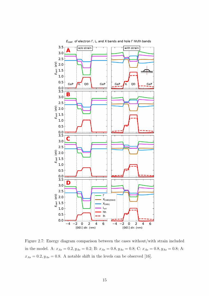
Figure 2.7: Energy diagram comparison between the cases without/with strain included
in the model. A: xAs = 0.2, yAs = 0.2; B: xAs = 0.8, yAs = 0.8; C: xAs = 0.8, yAs = 0.8; A:
xAs = 0.2, yAs = 0.8. A notable shift in the levels can be observed [16].
15

2.4.4 Coulomb interaction
In the situation that more than one carrier is confined within the QD, Coulomb interaction,
correlation (changes in the orbital shape due to Coulomb interaction) and exchange effects
(Pauli exclusion principle) 2 arise [30], leading to the formation of distinct multiparticle
states. The formation of these states may alter the absorption spectra and therefore the
properties of the dot; any complete theory must take them into account. They can be
calculated using the CI method [16], which consists of a basis expansion of the excitonic
Hamiltonians into Slater determinants. Hence, Schrodinger equation for this states reads:
HM |M〉 = EM |M〉 (2.22)
where EM is the eigenenergy and |M〉 are the multiexcitonic states corresponding to
Ne and Nh (number of electrons and holes respectively). The eigenstates of study are
M = X0,X+,X−,XX0, i.e., the neutral exciton X0 (Ne = 1, Nh = 1),the positive trion
X+ (Ne = 1, Nh = 2), the negative trion X− (Ne = 2, Nh = 1) and the neutral biexciton
XX0 (Ne = 2, Nh = 2). These states are, at the same time, described in terms of the
single-particle eigenfunctions Eq.(2.23). For example, for the neutral exciton X0
|X0〉 =Ne∑i=1
Nh∑j=1
ηij
∣∣∣∣∣∣ψei(~re) ψei(~rh)
ψhj(~re) ψhj(~rh)
∣∣∣∣∣∣ (2.23)
In general, Eq.(2.23) and the equivalent for the other excitons are expressed as an
expansion in Slater determinants functions, i.e.:
|M〉 =∑m
ηm|DMm 〉 (2.24)
where m runs over electron and hole configurations, and the coefficients obey the
normalization constraint∑
ν |ην |2 = 1. With this settled up, the system of equations to
be solved variationally is: ∑ν
〈DMn |HM |DM
m 〉ηm = EMηn (2.25)
The Hamiltonian can be decomposed in two components: HM = HM0 + V M , H0 the
non-interacting term of the Hamiltonian and V M introduces the Coulomb interaction.
The matrix elements in the basis of Slater determinants are:2A theory of how Pauli exclusion principle and correlation affect the absorption of photons by the
QDs has not been proposed yet. They may alter the number of total absorbed photons and, therefore,
the current. Further research in this topic should be done.
16
〈DMn |HM |DM
m 〉 = 〈DMn |HM
0 |DMm 〉+ 〈DM
n |V M |DMm 〉 (2.26)
The matrix elements of the Coulomb interaction are:
〈DMn |V M |DM
m 〉 =1
4πε0
∑ijkl
∫ ∫d~r1d~r2
qjqiε(~r1, ~r2)|~r1 − ~r2|
·
[φ∗i (~r1)φ∗j(~r2)φk(~r1)φl(~r2)− φ∗i (~r1)φ∗j(~r2)φl(~r1)φk(~r2)] =∑ijkl
(Vij,kl − Vij,lk)(2.27)
where qi, qj ∈ [−e,+e]. The first term on the integral would correspond to the direct
Coulomb interaction whereas the second one to the exchange Coulomb interaction. V is
defined as:
Vij,kl = (1− δij)(1− δkl)∫d~r1d~r2ψ
∗i (~r1φ
∗j(~r2)
(qiqj
4πε|~r1 − ~r2|
)φk(~r1)φ(~r2) (2.28)
Finally, the complete Hamiltonian components in the Slater determinant basis reads:
HMnm = 〈DM
n |HM |DMm 〉 =
ξ
(e)n − ξ(h)
n + 12
∑i,j∈Sn
(Vij,ij − V ij, ji), if n=m
12
∑j∈Sn
Vij,kj − Vij,jk, n,m differ by one particle state
12(Vij,kl − Vij,lk), n,m differ by two particle state
(2.29)
where ξ(e)n and ξ
(h)n is the sum of energies of the occupied single-particle (electrons and
holes) states in the Slater determinant. The calculus of the six-fold integral Eq.(2.28)
shows a demanding numerical procedure, which can be optimized using Green’s function
method. The numerical procedure will not be developed here, a further discussion on this
topic may be found in [16].
2.4.5 Optical Properties
The optical properties of the QDs are the key part of their analysis, because they allow
to define their suitability as photodetectors. The processes that may occur in the dot
are intraband and interband transitions, which can lead to absorption and recombination.
Intraband transitions happen within the same band (electron decay in the same band e.g.),
whereas interband occurs between the valence and conduction bands. Decay probability
is computed using Fermi’s Golden rule; absorption and recombination are a sum of the
different possible transitions. Putting it into math:
17
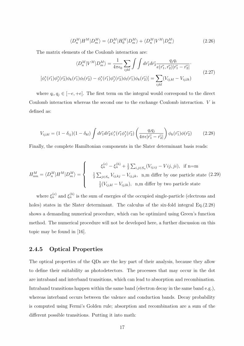
Figure 2.8: Absorption coefficient for a InAs/GaAs QD with base width 124A and height
62A.The plane polarization is absorbed much more efficiently than the z-polarization [12].
P =∑n,m
〈ψnf |∇|ψmi 〉, (2.30)
〈ψnf |∇|ψmi 〉 =8∑j,k
〈FjuΓj |∇|FkuΓ
k〉 =8∑j,k
[δj,k〈Fj|∇|Fk〉+ 〈Fj|Fk〉〈uΓ
j |∇|uΓk〉]
(2.31)
The radiative or recombination rate is defined:
R ≡ Γfi =( em
)2 2~ωc3|〈f |e · P |i〉|2 (2.32)
Here, ~ω stands for the radiation energy, |i〉, |f〉 for the multi-particle states (Eq.(2.24)),
|ψi〉, |ψf〉 for the single-particle states. In addition, Fj is the envelope function, and ~e the
polarisation vector. The absorption coefficient can be estimated as follows:
α(~ω) =πe2~
ε0n0cm20V
∑f
1
~ω|~e · P |2 1√
2πσexp
((E − ~ω)/2σ2
)(2.33)
This coefficient will be key in the design of photodetectors and is, for QD, extremely
peaked (see Fig. 2.8 and Section 2.5); basically, it describes how well radiation can be
absorbed depending on the energy. This absorption spectra is tunable by adjusting the
size of the dots, what makes them interesting for photodetection as well as emitting almost
monochromatic light. This topic will be covered in more detail later on, in Chapter 3.
The gain of the material is given by:
18

Figure 2.9: a) Mini-band as a function of the interdot distance. b) Mini-band as a function
of size (for H=15nm) [21].
g(~ω) =πe2~ncm2V
∑ij
|~e · P |2 1
π
· ~/τ(Ee
i − Ehj − ~ω)2 + (~/τ)2
(f e(Eei )− fh(Eh
j ))2
(2.34)
The gain is important to estimate the Quantum Efficiency (both internal and external)
of any photodetector. It is related with the number of charge carrier pairs created as a
function of the incident radiation, i.e., number and energy of incident photons.
2.4.6 Mini-band formation
So far interactions and energy levels within the QD have been covered, however considerations
about how QDs interact among them have not been taken into account. When they are
placed close to each other, a significant wavefunction overlap arise and the discrete energy
levels split into mini bands. For this case, discrete does not refer to the energy levels of
the own QD, but to the non-interference of them. In Fig. 2.9, the energy levels are plotted
against the distance between QDs of an array (a) and against the size of the QD (b):
As interdot distance increases and wavefunction overlap decreases, mini-bands reduce
to discrete levels, which is clear in Fig. 2.9 a). In Fig. 2.9 b) mini-bands show a discrete
behaviour which turns to continuum above the barrier potential.
In following sections, and taking as reference the results obtained in [21], QDs arrays
will be thought to be composed of single QDs that do not interact among them. This is
to very short distance a good approach, simplifying the calculi required.
19
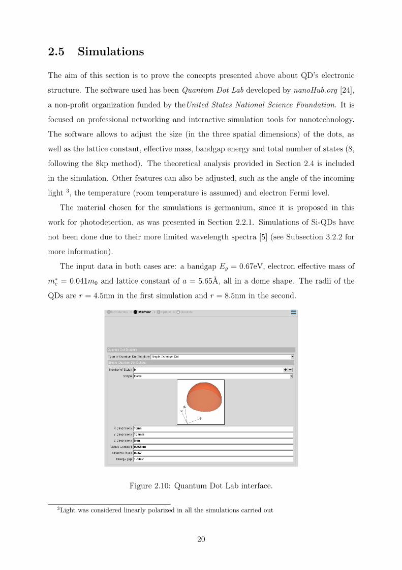
2.5 Simulations
The aim of this section is to prove the concepts presented above about QD’s electronic
structure. The software used has been Quantum Dot Lab developed by nanoHub.org [24],
a non-profit organization funded by theUnited States National Science Foundation. It is
focused on professional networking and interactive simulation tools for nanotechnology.
The software allows to adjust the size (in the three spatial dimensions) of the dots, as
well as the lattice constant, effective mass, bandgap energy and total number of states (8,
following the 8kp method). The theoretical analysis provided in Section 2.4 is included
in the simulation. Other features can also be adjusted, such as the angle of the incoming
light 3, the temperature (room temperature is assumed) and electron Fermi level.
The material chosen for the simulations is germanium, since it is proposed in this
work for photodetection, as was presented in Section 2.2.1. Simulations of Si-QDs have
not been done due to their more limited wavelength spectra [5] (see Subsection 3.2.2 for
more information).
The input data in both cases are: a bandgap Eg = 0.67eV, electron effective mass of
m∗e = 0.041m0 and lattice constant of a = 5.65A, all in a dome shape. The radii of the
QDs are r = 4.5nm in the first simulation and r = 8.5nm in the second.
Figure 2.10: Quantum Dot Lab interface.
3Light was considered linearly polarized in all the simulations carried out
20

First Simulation (I)
The simulation yields a bandgap energy of 2.114eV, much higher than the original 0.667eV;
this proves how the electronic structure of the semiconductor is affected by the strain
energy necessary to form the QD. The diagram shows the first and second excited states,
proving the atom-like behaviour of nano-scaled QDs.
The absorption profile has also been calculated: two sharp peaks, corresponding
to the first and the second excited state are observed. They occur at the energies
of 2.114 eV (586.2 nm) and 2.476 eV (500.3 nm) respectively. The absorption under
radiation is quantized in discrete values, each one corresponding to a peak (an excited
state). According to Fig. 2.11 and Fig. 2.12, this QD configuration will be suitable for
photodetection within the visible spectrum (green colour, to be precise).
In Fig. 2.12, a comparison between the absorption peaks at different polarization
angles is given: For θ = 0◦, the absorption peak occurs at the first excited level, whereas
for θ = 90◦ it occurs at the second one. Polarization angle φ was kept at 0◦ in both
cases. This effect must be addressed and corrected in the design of any photodetector, for
example using lenses that filter the light to the desired polarization. For instance, for a
perpendicularly polarized ray (θ = 0◦), there will be an unique sharp peak of absorption,
so in principle no colour filter would be necessary (see Subsection 3.1.1).
Figure 2.11: Absorption spectrum of the Ge QDs (I).
21

Figure 2.12: Comparison of the absorption spectra for different polarization angles (I).
Second Simulation
In this case, the band gap energy decreases to 0.5673 eV (around 0.10 eV less than the bulk
Ge) and the second excited state is placed 0.6514 eV above the ground state. Although the
radius difference is only 4 nm larger than in the first case, the differences are significant.
Therefore, an extremely precise control on QDs is required to allow absorption of light in
the desired wavelength.
The absorption peaks are completely shifted from the ones of the first simulation:
the first one happens at 0.5673 eV (2.184µm) and the second at 0.6514 eV (1.902µm).
Photodetection still remains possible, but this time within the SWIR range. Again, a
sweep from polarization angle θ from 0◦ to 0◦ yields to absorption peaks at the angle
boundaries; polarization angle should also be corrected with a filter.
These simulations have been useful to prove the atom-like behaviour of QDs, as well
as their tunability depending on the size. However, precise simulations should be carried
out using more complex simulations, considering not only the QDs, but also the layers
that surround them and have an influence in absorption too. Without that all-in-one
simulation, a description of the optoelectronic characteristics of a QDPD is incomplete.
It is, however, beyond the scope of the present thesis. Experimental results reported from
proof-of-concept devices will be provided in Chapter 3 instead.
22
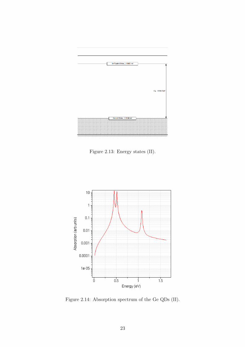
Figure 2.13: Energy states (II).
Figure 2.14: Absorption spectrum of the Ge QDs (II).
23
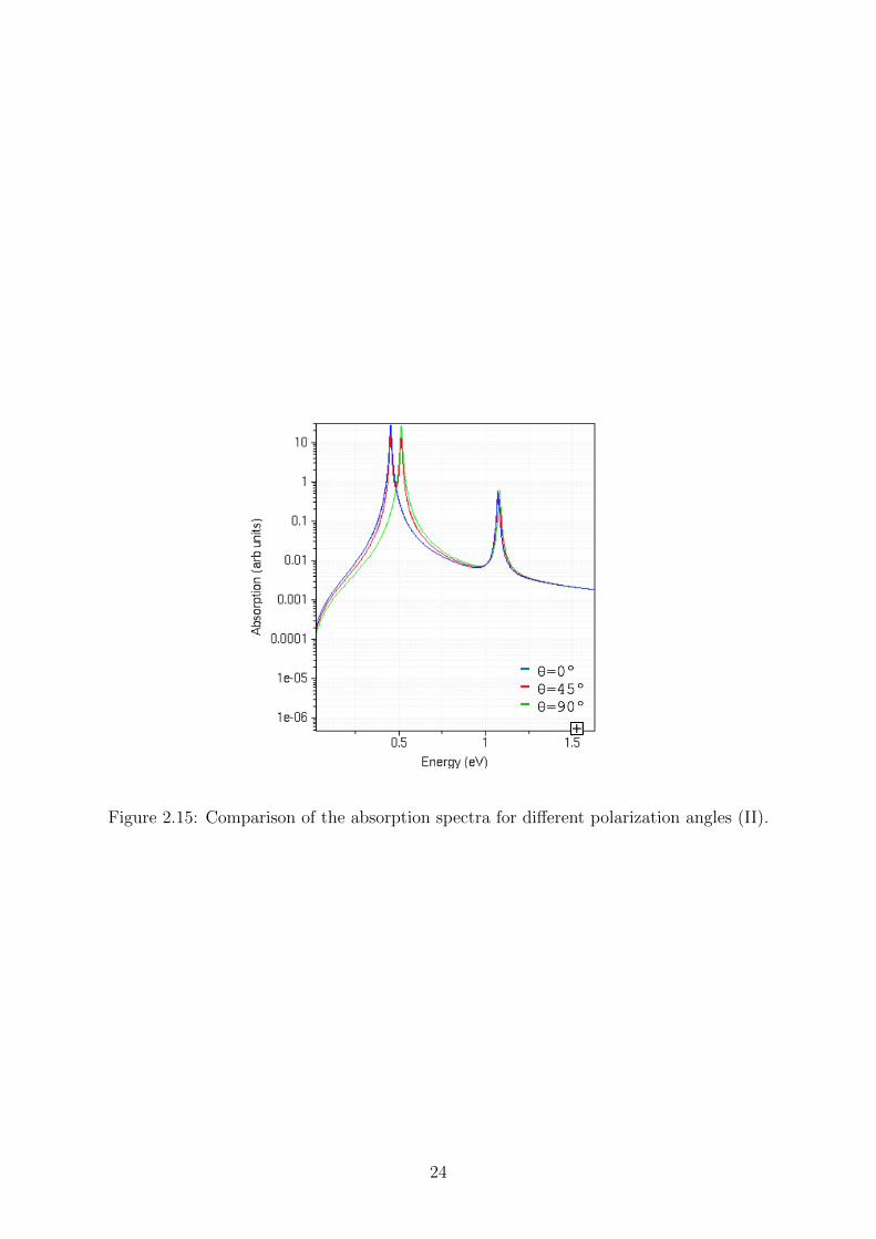
Figure 2.15: Comparison of the absorption spectra for different polarization angles (II).
24

Chapter 3
Photodetectors
3.1 State of the Art
3.1.1 Visible Spectrum
Colour sensing is the main goal of photodetectors, allowing to capture images within the
visible spectrum. This technology has experienced an outstanding improvement in the
last two decades, with the massive expansion of digital photography. Before introducing
the new sensing technologies based on QDs, a short discussion on the current state of art
of photodetectors is in order.
Colour sensing must cover wavelengths between 400 and 700nm approximately [18],[17],
absorbing the incident radiation and transforming it in an electrical signal. Apart from
imaging, colour photodetection is widely used in spectroscopy, fluorescent biomedical
imaging, industrial inspection, etc. [26][22][28][40]. Silicon devices are of common use in
this part of the spectrum, due to their good optical properties, abundance and developed
manufacturing techniques. Although there are many kinds of silicon photodetectors, the
two main types are photodiodes and photogates. Both are based on the photoelectric
effect, first explained by Einstein [9]. Basically, they convert the incident photon flux of
light in electron-hole pairs. If a photon has sufficient energy it will excite an electron from
the valence band and promote it to the conduction band, where electrons can move freely.
This sufficient energy is the band gap energy (Eg = 1.124 eV for Silicon [34]) and, when
applied, creates an electron-hole pair.
Under certain bias conditions, some of the pairs are converted into photocurrent. This
25

Figure 3.1: Simplified diagram showing the absorption and emission processes in a
semiconductor [27].
current is in the order of nA, pA, so it has to be integrated with the help of a capacitor;
in this process the main difference between CCDs and CMOSs arises. More information
of CCDS and CMOSs sensors can be found in Appendix B.
Photodiode
It is composed by an implanted n-region buried in a p- substrate, creating a depletion
area between them. This zone is depleted of carriers and has a certain electric field; this
electric field pushes the electrons to the n region, and holes to the p region, generating a
photocurrent. Photodiodes are usually operated in reverse bias, with a positive voltage
between n and p region. The generated current is then transferred to the read-out
circuit and interpreted. Focusing on the performance, photodiodes are limited to a 100%
quantum efficiency (one charge carrier per photon, at most). Transient times (also called
temporal photoresponse) are within the range of the nanoseconds, enough to fulfill the
requirements of imaging. Any new technology aiming to replace Si-based photodiodes
should exhibit figures of merit of this order [18].
Photogate
The photogate consists in a silicon gate buried in an insulator (typically SiO2), with a
depletion region below. Due to the electric field in the depletion region, charge carriers are
separated and either electrons or holes are collected by the photogate. For instance, for
a p- substrate with a n channel region near the surface (Fig. 3.3), the photogate collects
electrons. The electrons and holes pairs are created in the depletion region; electrons are
26

Figure 3.2: Diagram of an standard silicon photodiode [18].
Figure 3.3: Cross section of a photogate [18].
held in the potential well, while holes are collected in the substrate.
Typically, photogates are less efficient because of the photon absorption in the gate.
This effect can be counteracted using other materials for the gates such as Indium Tin
Oxide (ITO), which will also be used to improve QDPD efficiency [18] [23].
Pixel Optics
Each of the sensing parts in a sensor are called pixels: they are the minimum detecting
unit of digital image. Within a pixel, different parts can be identified: the microlens,
filter, passivation, metal and the substrate.
The microlens focuses the incident light on the detector, to optimise the absorption
of incoming photons. The colour filter is used to spectrally separate incoming photons,
allowing pixels to have different responsivities. In a RGB system, called Bayer Pattern,
27

Figure 3.4: CMOS image sensor, layer by layer [18].
every pixel detects a certain colour and then the software reconstructs the full colour
image with the information of each of the pixels. A more sophisticated colour pattern is
the quad pixel sensor 4.
Photodiodes are found under the colour filter, followed by a metal structure whose
main task is to transport the charges. On the bottom is the base of the pixel, the Si
substrate, which is responsible for photon absorption.
3.1.2 Infrared spectrum
Infrared detectors, though less used than sensors in the visible spectrum, are experiencing
an outstanding increase in the number of possible applications. Besides night surveillance
(their first application, for military and civil purposes), they are being used for optical
tomography, process monitoring, Lidar sensors, advanced driver’s assistance (obstacles
detection), augmented reality, biometrics, etc. [23][28]. Many of these applications require
high fidelity and a massive production of these IR detectors at a low cost. Silicon-based
products, though cheap and highly optimised, are not suitable for these tasks, because of
the Si absorption decreases around wavelengths of 900 nm [22].
A short discussion about infrared radiation is in order, to understand the range of
possible applications for QDPDs. Infrared covers the range from approximately 0.75 µm
to 12 µm; within this range, different regions can be distinguished: Near-Infrared (NIR),
4Difference among them in https://news.skhynix.com/evolution-of-pixel-technology-in-cmos-image-
sensor/
28
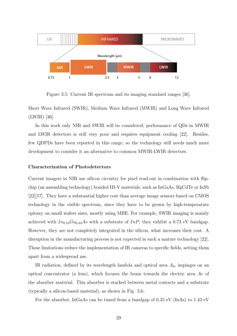
Figure 3.5: Current IR spectrum and its imaging standard ranges [36].
Short Wave Infrared (SWIR), Medium Wave Infrared (MWIR) and Long Wave Infrared
(LWIR) [36].
In this work only NIR and SWIR will be considered; performance of QDs in MWIR
and LWIR detectors is still very poor and requires equipment cooling [22]. Besides,
few QDPDs have been reported in this range, so the technology still needs much more
development to consider it an alternative to common MWIR-LWIR detectors.
Characterization of Photodetectors
Current imagers in NIR use silicon circuitry for pixel read-out in combination with flip-
chip (an assembling technology) bonded III-V materials, such as InGaAs, HgCdTe or InSb
[22][17]. They have a substantial higher cost than average image sensors based on CMOS
technology in the visible spectrum, since they have to be grown by high-temperature
epitaxy on small wafers sizes, mostly using MBE. For example, SWIR imaging is mainly
achieved with In0.53Ga0.43As with a substrate of InP ; they exhibit a 0.73 eV bandgap.
However, they are not completely integrated in the silicon, what increases their cost. A
disruption in the manufacturing process is not expected in such a mature technology [22].
These limitations reduce the implementation of IR cameras to specific fields, setting them
apart from a widespread use.
IR radiation, defined by its wavelength lambda and optical area A0, impinges on an
optical concentrator (a lens), which focuses the beam towards the electric area Ae of
the absorber material. This absorber is stacked between metal contacts and a substrate
(typically a silicon-based material), as shown in Fig. 3.6.
For the absorber, InGaAs can be tuned from a bandgap of 0.35 eV (InAs) to 1.43 eV
29
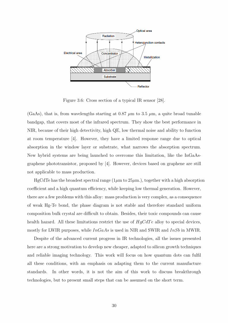
Figure 3.6: Cross section of a typical IR sensor [28].
(GaAs), that is, from wavelengths starting at 0.87 µm to 3.5 µm, a quite broad tunable
bandgap, that covers most of the infrared spectrum. They show the best performance in
NIR, because of their high detectivity, high QE, low thermal noise and ability to function
at room temperature [4]. However, they have a limited response range due to optical
absorption in the window layer or substrate, what narrows the absorption spectrum.
New hybrid systems are being launched to overcome this limitation, like the InGaAs-
graphene phototransistor, proposed by [4]. However, devices based on graphene are still
not applicable to mass production.
HgCdTe has the broadest spectral range (1µm to 25µm.), together with a high absorption
coefficient and a high quantum efficiency, while keeping low thermal generation. However,
there are a few problems with this alloy: mass production is very complex, as a consequence
of weak Hg-Te bond, the phase diagram is not stable and therefore standard uniform
composition bulk crystal are difficult to obtain. Besides, their toxic compounds can cause
health hazard. All these limitations restrict the use of HgCdTe alloy to special devices,
mostly for LWIR purposes, while InGaAs is used in NIR and SWIR and InSb in MWIR.
Despite of the advanced current progress in IR technologies, all the issues presented
here are a strong motivation to develop new cheaper, adapted to silicon growth techniques
and reliable imaging technology. This work will focus on how quantum dots can fulfil
all these conditions, with an emphasis on adapting them to the current manufacture
standards. In other words, it is not the aim of this work to discuss breakthrough
technologies, but to present small steps that can be assumed on the short term.
30
3.2 QD Photodetectors
Quantum Dot photodetectors are a promising new technology to overcome existing IR
sensors and even VIS-Si sensors. They have important advantages, such as: spectral
sensitivity control of the detectors by QD size, detection under normal incidence of light,
lower price (in IR sensing, mostly), processing on a large area, smaller pixel pitch, etc
[8],[40]. Active research has been carried out in the last decade, what has brought QDPD
to technological readiness level 3 [22], although the SWIR camera reported by SWIR
Vision Systems [36] proves that the posible next stage has been achieved. This method
for judging the maturity of technologies was first proposed by the NASA [38] and has
become an standard within the UE too. Level 3 means that an active level of research
has been reached and a proof-of-concept has been constructed. The main targets to bring
QDPD to an industrial level can be summarized in three points: material, device and
camera integration challenges.
Material challenges include finding the right component for the dot, considering how
its properties vary from the bulk material to the final dot and adjusting them to the
spectrum to be detected. In following sections, behaviour on this topic for lead sulphide
(PbS) and germanium (Ge) will be further explained. The other aspect that should not
be forgotten is material’s cost for scale-up production, availability in different parts of the
world and non-dependence on a single supplier [26]. In the case of PbS, the estimated
cost of active material per photodetector is around 0.15 US Dollar (0.13€) and similarly
with Germanium QDs. For a production of 10 million devices, 50kg of material would be
required, what can be easily covered by annual production [22]. Thus, materials are not
a limiting factor.
Device challenges include knowing accurately the electronic structure of the QDs and
transitions involved in photon absorption. These are well known for bulk semiconductors,
but not with the same level of detail in QDs. One of the latest models published has been
introduced in Chapter 2, but light-matter coupling, low current, good responsivities, etc
must be further investigated.
Camera integration is the last step to be solved before mass production. Quantum
Dot photodetectors must be compatible to the current industrial fabrication flow based
on Silicon, to allow process optimization and consequently low prices. Besides, standard
camera sizes should be achieved. In following sections these steps will be addressed, giving
31
Figure 3.7: Schematic comparison of EQE between silicon, InGaAs and PbS QDs [23].
a complete picture of the advances carried out in this research field.
3.2.1 PbS Quantum Dot Photodetectors
Colloidal Quantum Dots have reached an established status as light sources in displays
[29], what has increased the interest in other applications such as infrared detection.
Great progress has been achieved in QDs sensing technology in the recent years, enough
to consider them a viable option for mass market applications.
PbS QDs enable the detection in the NIR, SWIR, due to their tunable optical properties
depending on the size. By varying the dot size from 2 nm to 10 nm, the whole SWIR
spectrum can be covered (700-1800 nm) [17]. In Fig. 3.7, a comparison of the absorption
spectra between standard silicon (for the visible spectrum) and InGaAs (for the IR) is
plotted. Taking advantage of the large exciton Bohr radius, PbS QDs cover most of the
range of wavelengths of interest, while showing a better external quantum efficiency.
QD size has a strong influence in the optical properties, as it has been shown in Section
2.5, being the absorption peak linearly dependent with the size, according to [23]. For
example, a QD with diameter 5.5nm has an absorption peak around 1440nm, while dots
as big as 10nm diameter have been reported [8] (for photodetection). With such small
dots, the pixel pitch limit is set by the CMOS ROIC, unlike in InGaAs sensors.
Fabrication Process
PbS photodiodes are designed with an n-p junction architecture. The fabrication process
starts by cleaning the substrates (Si/SiO2) with a standard detergent. Then, a metal
oxide electron transport layer (ETL) is deposited on the substrate, acting as the bottom
32

Figure 3.8: Absorption peak depending on dot size [23].
contact, to improve electron transport. TiOx, ZnO or TiN are used for this layer, thanks
to their high reflectivity in the IR range and compatibility with the CMOS process. This
layer is annealed at high temperature, which makes it interesting for deposition before
the QD layer (to avoid melting). Another approach for this layer under development is
the use of Transition Metal Dichalcogenide (TMDC) for high-mobility transport layers
[35]. They can provide good IR absorption as well as a good transfer of charges to the
contacts for charge collection. MoS2 and WS2 have been proposed for this layer.
Afterwards the QD film is deposited layer by layer: the colloidal QD solution is
deposited by spin-coating in the ETL layer (15 − 50 nm each time) and repeated until
the desired height is obtained. The thickness is a trade-off: the thicker it is, the more
photons that are collected, but the more difficult to assemble. As explained in Section
2.3.1, QDs may also be printed according to recent studies [35]. On top of the stack a
hole transport layer is deposited, a p-type polymer, designed to transport the holes. For
example, in [35] the material chosen was Spiro, named after ,2’,7,7’-Tetrakis[N,N-di(4-
methoxyphenyl)amino]-9,9’-spirobifluorene, a perovskite commonly used for hole transport
layers (HTL). The QD structure is finished with a semi-transparent top contact that
allows top-side illumination, usually made of evaporated silver (Ag) or sputtered ITO. An
optimised version of an ITO top contact is able to significantly improve the light harvesting
and thus EQE, while preventing electron’s back injection. A convenient solution for this
layer manufacture is presented in [26]: gold source and drain contacts are patterned on
the TMDCs using photolithography; this might speed up production.
33

Figure 3.9: Cross image of the QD stack, obtained using annular bright field scanning
transmission electron microscopy [8].
Figure 3.10: Cross view of the stack, schematic (left) and obtained by transmission
electron microscopy [23].
Figure 3.11: Photodetector with circuit diagram, includind the TMDC layer [26].
34

Figure 3.12: Scanning electron microscopy representing the full QD stack [35].
QD Performance
A proper evaluation of the QD photodetector properties is necessary to judge whether
they can be a feasible alternative for IR sensing. The main figures of reference will be
analysed here and compared with well-established technologies presented before.
The first value to consider is the dark current Id, measured at room temperature.
In [8], a value of 29 nA/cm2 at an applied reverse bias of -1V is reported, showing a
photocurrent-to-dark current ratio of 90dB. Meanwhile, in [23] 6 µA/cm2 at reverse bias
-2V. The reference value for an InGaAs detector is below 20 fA/cm2: PbS QDs cannot
beat this target value, although presents a sufficiently low value for imaging purposes.
It is of interest to remark how dark current can be drastically reduced by cooling the
equipment: at 193K, dark current ratio was improved from 30dB at room temperature to
62dB [23]. However, the aim of this work is to provide solutions for standard utilization
at room temperatures, without cooling. In both cases a linear scaling of dark current with
pixel size is observed, an important result to achieve high resolution devices.
The EQE achieved is of 21% on top illuminated devices for λ = 940 nm [8], raising to
25% with optimized semi-transparent contacts [23] at λ = 1440 nm. A detailed graphic
of the EQE as a function of the wavelength is provided in Fig. 3.13; it can be seen that
the higher efficiency is achieved within the VIS spectrum, with peaks of 90% (for the
QD configuration chosen), and drastically decreases over λ = 1000 nm. These values are
lower than InGaAs based photodetectors, but still higher than Si PD. The detectivity D∗
rises to 1012 cmHz1/2W−1 in both [35][8], same as for TMDCs hybrid PD, with 1012 Jones
35

Figure 3.13: EQE comparison for different bias voltages and wavelengths [35].
5 (WS2) and 2.8 · 1012 Jones (MbS2) [26], whereas an average InGaAs detector shows a
detectivity of 6 · 1012 Jones.
Another figure of merit is the photo-response, which shows how fast photocurrent is
conducted. First, the rise time from 10% to 90% of the photogenerated signal is measured
(τrise) and then the fall time (90% to 10%). Rise and fall times of 57 µs and 86 µs were
obtained under perpendicular illumination in [8], further improving this value in [23]
to 13 µs and 41 µs. This performance is sufficient for basic imaging applications, but
shorter times should be achieved for more demanding imaging applications (high speed
cameras, video, etc). Limiting factors, like trap states or interface defects, should be
further investigated, to approximate them to values registered in InGaAs PD (τrise = 0.65
µs, τfall = 2.20 µs [4]. For TMDC hybrid devices, τrise = 0.032 µs(WS2) and τfall = 0.20
µs (MbS2), under illumination λ = 1310 nm. Ink-printed QD yield values of τrise = 4.4
µs and τfall = 8.2 µs [35] [26]. In these devices, response is far from the benchmark values
of current technologies. This might be caused by trapped electrons in the QD, that limit
the charges flow to the transport layers.
Integration Aspects
QD photodetectors under investigation and testing phase are mostly manufactured using
slow techniques, such as manual scrubbing for the cleaning of the contact pads. Any
currently standardised process for the mass market is based in photolithography, a highly
accurate fabrication process flow [10]. The next step to incorporate QDPD to cameras is
51 Jone is equal to 1 cm ·Hz1/2W−1
36

Figure 3.14: Transient photoresponse [23].
Figure 3.15: Transient photoresponse [8].
Figure 3.16: Relaxation times [26].
37
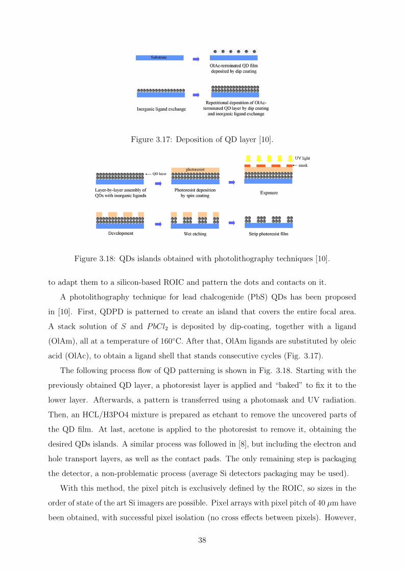
Figure 3.17: Deposition of QD layer [10].
Figure 3.18: QDs islands obtained with photolithography techniques [10].
to adapt them to a silicon-based ROIC and pattern the dots and contacts on it.
A photolithography technique for lead chalcogenide (PbS) QDs has been proposed
in [10]. First, QDPD is patterned to create an island that covers the entire focal area.
A stack solution of S and PbCl2 is deposited by dip-coating, together with a ligand
(OlAm), all at a temperature of 160◦C. After that, OlAm ligands are substituted by oleic
acid (OlAc), to obtain a ligand shell that stands consecutive cycles (Fig. 3.17).
The following process flow of QD patterning is shown in Fig. 3.18. Starting with the
previously obtained QD layer, a photoresist layer is applied and “baked” to fix it to the
lower layer. Afterwards, a pattern is transferred using a photomask and UV radiation.
Then, an HCL/H3PO4 mixture is prepared as etchant to remove the uncovered parts of
the QD film. At last, acetone is applied to the photoresist to remove it, obtaining the
desired QDs islands. A similar process was followed in [8], but including the electron and
hole transport layers, as well as the contact pads. The only remaining step is packaging
the detector, a non-problematic process (average Si detectors packaging may be used).
With this method, the pixel pitch is exclusively defined by the ROIC, so sizes in the
order of state of the art Si imagers are possible. Pixel arrays with pixel pitch of 40 µm have
been obtained, with successful pixel isolation (no cross effects between pixels). However,
38
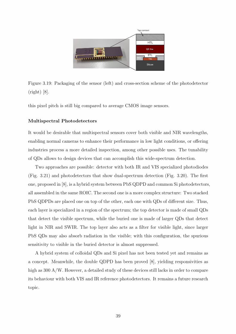
Figure 3.19: Packaging of the sensor (left) and cross-section scheme of the photodetector
(right) [8].
this pixel pitch is still big compared to average CMOS image sensors.
Multispectral Photodetectors
It would be desirable that multispectral sensors cover both visible and NIR wavelengths,
enabling normal cameras to enhance their performance in low light conditions, or offering
industries process a more detailed inspection, among other possible uses. The tunability
of QDs allows to design devices that can accomplish this wide-spectrum detection.
Two approaches are possible: detector with both IR and VIS specialized photodiodes
(Fig. 3.21) and photodetectors that show dual-spectrum detection (Fig. 3.20). The first
one, proposed in [8], is a hybrid system between PbS QDPD and common Si photodetectors,
all assembled in the same ROIC. The second one is a more complex structure: Two stacked
PbS QDPDs are placed one on top of the other, each one with QDs of different size. Thus,
each layer is specialized in a region of the spectrum; the top detector is made of small QDs
that detect the visible spectrum, while the buried one is made of larger QDs that detect
light in NIR and SWIR. The top layer also acts as a filter for visible light, since larger
PbS QDs may also absorb radiation in the visible; with this configuration, the spurious
sensitivity to visible in the buried detector is almost suppressed.
A hybrid system of colloidal QDs and Si pixel has not been tested yet and remains as
a concept. Meanwhile, the double QDPD has been proved [8], yielding responsivities as
high as 300 A/W. However, a detailed study of these devices still lacks in order to compare
its behaviour with both VIS and IR reference photodetectors. It remains a future research
topic.
39

Figure 3.20: Responsivity comparison of three configurations of QD detectors (left) and
diagram of the dual stack multispectral QDPD (right) [17].
Figure 3.21: Schematic figure of a hybrid multispectral sensor, composed by a Si pixel
and a QDPD [8].
40
3.2.2 Ge Quantum Dot Photodetectors
Group IV quantum dots have attracted much interest due to their compatibility with
Si technology and very large-scale integration possibilities. Like PbS QDs, they can
offer tunability from UV to IR, while showing a high quantum efficiency. Although
Silicon QDs are easier and cheaper to manufacture, they have a more limited wavelength
spectra. Germanium QDs, while still highly compatible with Si substrates and fabrication
processes, offer a wider spectrum, lower synthesis temperature and larger excitonic Bohr
radius (stronger quantum confinement) [5][32]. Besides, it has higher carrier mobility
than Si, is non-toxic, electro-chemically stable in time and relatively cheap compared to
other options (such as InGaAS).
Highly accurate manufacture of these devices is a key factor to guarantee uniformity
of the optoelectronic features. Defects, mid-gap states or the degree of crystallization may
affect the performance of Ge-based devices.
Fabrication process
Different fabrication processes have been reported, using different deposition techniques.
In [19], QDs were grown by ultrahigh-vacuum chemical deposition on a Si buffer layer of 50
nm. After deposition, self-assembled dots were formed at 600◦C under Stranski-Krastanov
mode. Another fabrication process consists in using rf-magnetron sputtering 6 deposition
of SiO2 and Ge on a n-Si substrate, maintained at 400◦C [5] [32]. The deposited film is
then annealed at 500◦C in a N2 atmosphere, in order to generate densely packed Ge QDs.
Thicknesses as low as 25 nm can be achieved, although they can also exceed hundreds of
nanometers.
Regarding the compatibility of Ge QD heteroepitaxy with the integration in CMOS
sensors, some issues must be addressed. Ge/Si growth imposes a hard constraint in
all the phases, mostly in surface cleaning. QD deposition should be one of the latest
steps, to prevent QDs arrays to be destroyed by any following high temperature process.
Likewise, in the formation of the dots high temperatures should be avoided, to protect
the underlying circuitry. Therefore, temperatures lower than 450◦C are required. In [42],
6Magnetron sputtering is technique based on bombarding a surface with high energy
ions, which are guided to the target by a magnetic field. More information available in
http://www.semicore.com/news/92-what-is-rf-sputtering.
41

Figure 3.22: Schematic view of a Ge QDPD on a silicon substrate [5].
Figure 3.23: Schematic view of a Ge QDPD on a silicon substrate [32].
a hydrogenation technique using hydrogen fluoride (HF) is proposed, achieving surface
preparation temperatures of 470◦C, which could be further lowered to 400◦C.
A top contact of either ITO or Indium-zinc-oxide (IZO) is sputtered to form the top
contact. As it happened with the lead sulphide (PbS) QDPDs, these materials are chosen
because of their high transparency in the visible and infrared range. With this treatment,
Ge-QDs gap energy is reported to be 1.6 eV, which is a good figure for VIS and even UV
(IR wavelengths can be absorbed too, though less efficiently).
QD Performance
A good performance in image sensing has been reported for Ge-based PD. Responsivities
can rise as high as 4 A/W, bias of -10 V, and to 1.75 A/W at a lower bias of -2 V. In
Fig. 3.24, a diagram of the responsivity at different bias and wavelengths is represented.
Responsivities as high as 10 A/W were obtained at -4 V bias, lowering to 1.5 A/W at
-2 V. Maximum responsivity is achieved in the 700-800 nm range (red-infrared) for high
bias, and is almost constant for a lower -2 V. Average silicon detector’s responsivities
range from 0.4 to 2.8 A/W, so values obtained with Ge QDs seriously challenge current
available technologies.
Another figure of merit is the Internal Quantum Efficiency (IQE). High values are
obtained, rising to 700% (-10 V bias) or 300% (-2 V bias) [5], and to 1700% (-4 V bias)
42

Figure 3.24: Responsivity and IQE depending on the wavelength
or 400% (-2 V bias). However, these are peak values; a more detailed image of how IQE
changes with incident wavelength and reverse bias is given in Fig. 3.24. An explanation
for this high photoconductive gain needs an insight on the internal behaviour of the
charges: electron-hole pairs are generated mostly in the Ge QDs, although the Si substrate
contributes too. Due to the difference in the effective mass, holes are heavier than electrons
and therefore slower in tunnelling between QDs. This causes a hole accumulation in the
Ge QDs layer. To keep charge neutrality, additional electrons have to be supplied from the
top contact (IZO, ITO), which tunnel through SiO2, increasing the total photocurrent.
This proves that both the Ge QDs and the Si substrate are fundamental to provide a wide
range of absorption.
Transient photoresponse is pretty low compared to PbS QDs; τrise, τfall measurements
yield values below 35 ns [32], although the experiment protocol was not the same, so
results cannot be directly compared. In any case, the response is fast enough for high-
speed devices.
43

Chapter 4
Conclusions
Insights on QDs state of the art have been provided in Chapter 2, with a focus on
fabrication and modelling of their optoelectronic properties. Many theoretical models
have been developed since the 90s, being the one proposed in this work one of the latest,
based on 8kp method, which has proved to yield the most accurate results. However, any
practical use of the dots must be adjusted with experimental data: size and shape can be
determined with microscopy techniques (AFM, TEM, for instance), whereas the electronic
structure landscape can be determined using transmission and absorption spectroscopy
[13].
Regarding Chapter 3, a brief introduction on currently available photodetectors has
been given, to compare its structure with the QDPD studied later. As it has been
explained, the most developed technology are PbS QDPDs, since many more scientific
publications have been published using this material. PbS based photodetectors are in
a much more advanced state of the art, with sensors already commercialized [36]. Fig.
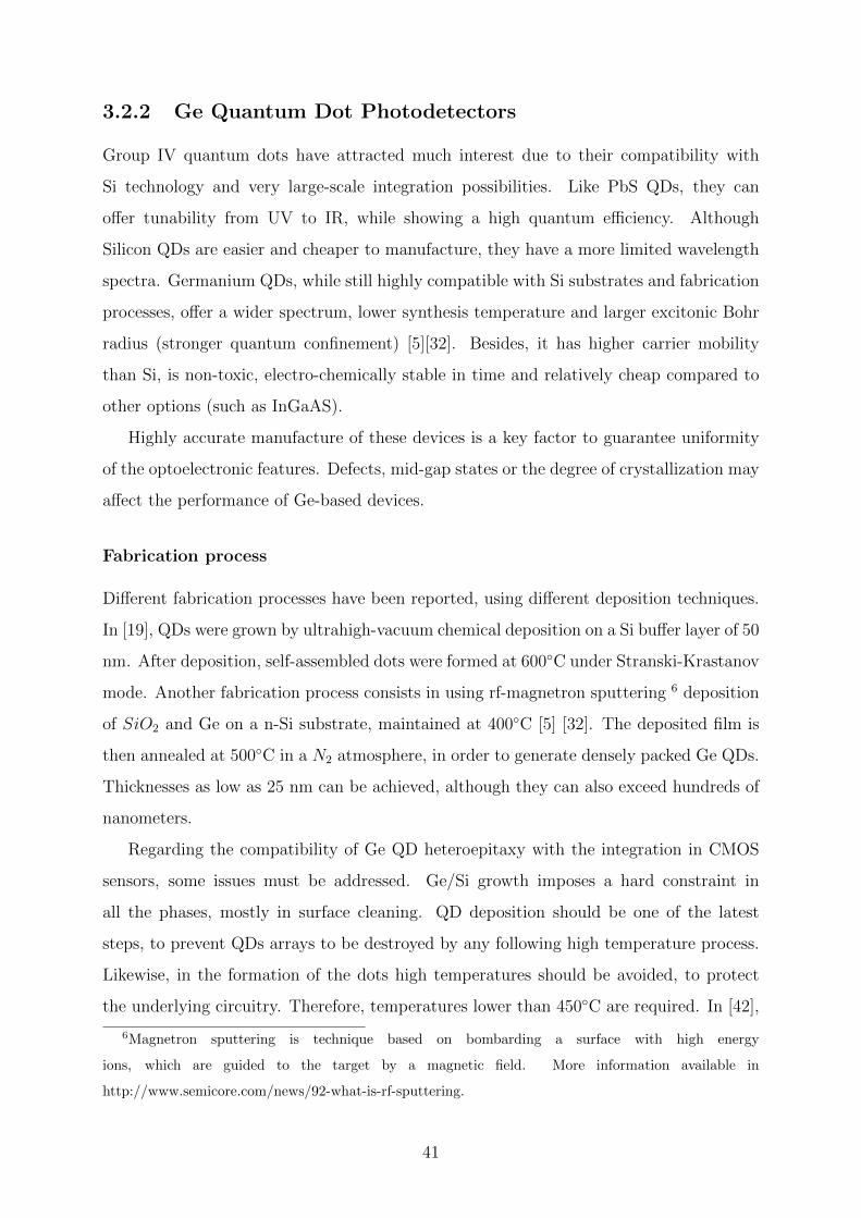
4.1 and Fig. 4.2 show two examples of pictures taken with a PbS QD-based camera, the
Acuros CQD 640/640L GigE SWIR Camera developed by Swir Vision Systems.
Despite of all the advances, some issues must still be addressed: improve detectivity,
achieve lower thermal noise, improve the resolution and reduce their cost to the level
of Si-based sensors. Another problem not mentioned yet is toxicity; in general, it is
most likely to see small bandgap transitions in heavy metals (Pb, Hg, e.g.), which have
the problem of being toxic. According to the WHO [25], lead is “a cumulative toxicant
that affects multiple body systems”. In very small quantities and well isolated from the
environment, there should be no risk at all. Nevertheless, a risk of exposure might arise
44
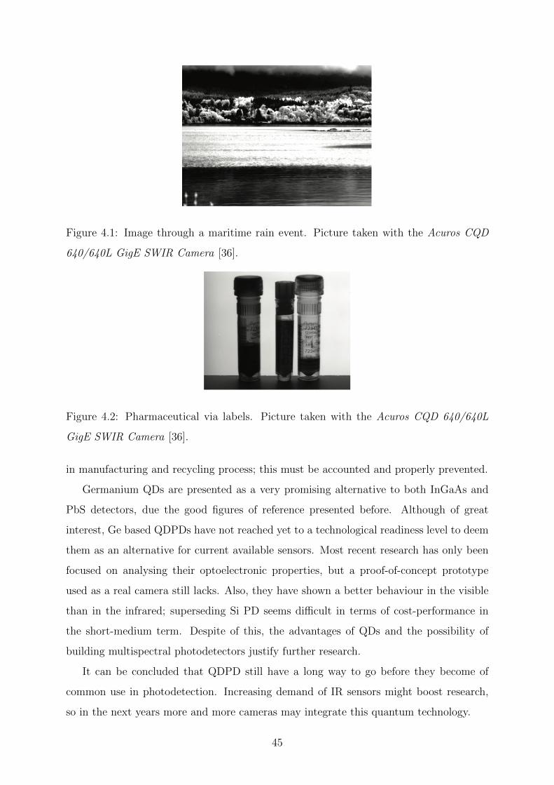
Figure 4.1: Image through a maritime rain event. Picture taken with the Acuros CQD
640/640L GigE SWIR Camera [36].
Figure 4.2: Pharmaceutical via labels. Picture taken with the Acuros CQD 640/640L
GigE SWIR Camera [36].
in manufacturing and recycling process; this must be accounted and properly prevented.
Germanium QDs are presented as a very promising alternative to both InGaAs and
PbS detectors, due the good figures of reference presented before. Although of great
interest, Ge based QDPDs have not reached yet to a technological readiness level to deem
them as an alternative for current available sensors. Most recent research has only been
focused on analysing their optoelectronic properties, but a proof-of-concept prototype
used as a real camera still lacks. Also, they have shown a better behaviour in the visible
than in the infrared; superseding Si PD seems difficult in terms of cost-performance in
the short-medium term. Despite of this, the advantages of QDs and the possibility of
building multispectral photodetectors justify further research.
It can be concluded that QDPD still have a long way to go before they become of
common use in photodetection. Increasing demand of IR sensors might boost research,
so in the next years more and more cameras may integrate this quantum technology.
45
Bibliography
[1] Antonio Arnau and David Soares. “Fundamentals on Piezoelectricity”. In: Piezoelectric
Transducers and Applications. Ed. by Antonio Arnau Vives. Berlin, Heidelberg:
Springer Berlin Heidelberg, 2004, pp. 1–37. isbn: 978-3-662-05361-4. doi: 10.1007/
978-3-662-05361-4_1. url: https://doi.org/10.1007/978-3-662-05361-4_1.
[2] Ralph Baierlein. “Thermal Physics”. In: Cambridge, U.K. ; New York : Cambridge
University Press, 1999. isbn: 978-0521658386.
[3] Elena Borovitskaya and Michael S Shur. Quantum Dots. WORLD SCIENTIFIC,
2002. doi: 10.1142/4934. eprint: https://www.worldscientific.com/doi/pdf/
10.1142/4934. url: https://www.worldscientific.com/doi/abs/10.1142/
4934.
[4] Gaoqi Cao et al. “Multicolor Broadband and Fast Photodetector Based on InGaAs
Insulator–Graphene Hybrid Heterostructure”. In: Advanced Electronic Materials 6.3
(), p. 1901007. doi: https://doi.org/10.1002/aelm.201901007. eprint: https:
//onlinelibrary.wiley.com/doi/pdf/10.1002/aelm.201901007. url: https:
//onlinelibrary.wiley.com/doi/abs/10.1002/aelm.201901007.
[5] S. Cosentino et al. “High-efficiency silicon-compatible photodetectors based on Ge
quantum dots”. In: Applied Physics Letters 98.22 (2011), p. 221107. doi: 10.1063/
1.3597360. eprint: https://doi.org/10.1063/1.3597360. url: https://doi.
org/10.1063/1.3597360.
[6] Yole Developpment. CMOS Image Sensor (CIS) Industry. url: http://www.yole.
fr/CMOS_Image_Sensors_Industry_Overview.aspx.
[7] Eric R. Fossum and Donald B. Hondongwa. “A Review of the Pinned Photodiode
for CCD and CMOS Image Sensors”. In: IEEE Journal of the Electron Devices
Society 2.3 (2014), pp. 33–43. doi: 10.1109/JEDS.2014.2306412.
46

[8] Epimitheas Georgitzikis et al. “Integration of PbS Quantum Dot Photodiodes on
Silicon for NIR Imaging”. In: IEEE Sensors Journal 20.13 (2020), pp. 6841–6848.
doi: 10.1109/JSEN.2019.2933741.
[9] David J. Griffiths and Darrell F. Schroeter. Introduction to Quantum Mechanics.
3rd ed. Cambridge University Press, 2018. doi: 10.1017/9781316995433.
[10] Chen Hu et al. “The micropatterning of layers of colloidal quantum dots with
inorganic ligands using selective wet etching”. In: Nanotechnology 25.17 (Apr. 2014),
p. 175302. doi: 10.1088/0957-4484/25/17/175302. url: https://doi.org/10.
1088/0957-4484/25/17/175302.
[11] Icinsights. CMOS Image Sensor Sales Stay on Record-Breaking Pace. url: https:
//www.icinsights.com/news/bulletins/CMOS-Image-Sensor-Sales-Stay-On-
RecordBreaking-Pace/.
[12] Hongtao Jiang and J. Singh. “Self-assembled semiconductor structures: electronic
and optoelectronic properties”. In: IEEE Journal of Quantum Electronics 34.7
(1998), pp. 1188–1196. doi: 10.1109/3.687862.
[13] Hongtao Jiang and Jasprit Singh. “Conduction band spectra in self-assembled InAs/GaAs
dots: A comparison of effective mass and an eight-band approach”. In: Applied
Physics Letters 71.22 (1997), pp. 3239–3241. doi: 10 . 1063 / 1 . 120302. eprint:
https://doi.org/10.1063/1.120302. url: https://doi.org/10.1063/1.
120302.
[14] Richard G Jones et al., eds. Compendium of Polymer Terminology and Nomenclature.
IUPAC Recommendations 2008. The Royal Society of Chemistry, 2009, P001–443.
isbn: 978-0-85404-491-7. doi: 10.1039/9781847559425. url: http://dx.doi.
org/10.1039/9781847559425.
[15] Yeongho Kim et al. “Effect of spacer layer thickness on structural and optical
properties of multi-stack InAs/GaAsSb quantum dots”. In: Applied Physics Letters
107.17 (2015), p. 173109. doi: 10.1063/1.4934695. eprint: https://doi.org/10.
1063/1.4934695. url: https://doi.org/10.1063/1.4934695.
[16] Petr Klenovsky, Andrei Schliwa, and Dieter Bimberg. “Electronic states of (InGa)(AsSb)
/GaAs/GaP quantum dots”. In: Physical Review B 100.11 (Sept. 2019). issn: 2469-
47

9969. doi: 10.1103/physrevb.100.115424. url: http://dx.doi.org/10.1103/
PhysRevB.100.115424.
[17] Gerasimos Konstantatos. “Colloidal quantum dot photodetectors”. In: Colloidal
Quantum Dot Optoelectronics and Photovoltaics. Ed. by Gerasimos Konstantatos
and Edward H.Editors Sargent. Cambridge University Press, 2013, pp. 173–198.
doi: 10.1017/CBO9781139022750.008.
[18] Michael Kriss. Handbook of Digital Imaging. John Wiley Sons, Ltd., 2015. Chap. 3.
isbn: 978-0-470-51059-9.
[19] M. H. Kuo et al. “Designer Ge quantum dots on Si: A heterostructure configuration
with enhanced optoelectronic performance”. In: Applied Physics Letters 101.22
(2012), p. 223107. doi: 10.1063/1.4768292. eprint: https://doi.org/10.
1063/1.4768292. url: https://doi.org/10.1063/1.4768292.
[20] E.M.Lifschitz L.D.Landau. Mecanica, volumen 1, Curso de Fısica Teorica. Editorial
Reverte, 1994.
[21] Olga L. Lazarenkova and Alexander A. Balandin. “Miniband formation in a quantum
dot crystal”. In: Journal of Applied Physics 89.10 (2001), pp. 5509–5515. doi: 10.
1063/1.1366662. eprint: https://doi.org/10.1063/1.1366662.
[22] Clement Livache et al. “Road Map for Nanocrystal Based Infrared Photodetectors”.
In: Frontiers in Chemistry 6 (2018), p. 575. issn: 2296-2646. doi: 10.3389/fchem.
2018.00575. url: https://www.frontiersin.org/article/10.3389/fchem.
2018.00575.
[23] Pawel E. Malinowski et al. “Thin-Film Quantum Dot Photodiode for Monolithic
Infrared Image Sensors”. In: Sensors 17.12 (2017). issn: 1424-8220. url: https:
//www.mdpi.com/1424-8220/17/12/2867.
[24] nanoHUB.org. On-line Simulation and More for Nanotechnology. url: http://
nanoHUB.org.
[25] World Health Organisation. Lead Poisoning and Health. url: https://www.who.
int/news-room/fact-sheets/detail/lead-poisoning-and-health.
48
[26] Onur Ozdemir et al. “High Sensitivity Hybrid PbS CQD - TMDC Photodetectors
up to 2 m”. In: ACS Photonics 2019 (Sept. 2019). doi: 10.1021/acsphotonics.
9b00870.
[27] Dr. Rudiger Paschotta. Responsivity. url: https://www.rp- photonics.com/
responsivity.html.
[28] Antoni Rogalski. “Infrared detectors: status and trends”. In: Progress in Quantum
Electronics 27.2 (2003), pp. 59–210. issn: 0079-6727. doi: https://doi.org/
10.1016/S0079-6727(02)00024-1. url: https://www.sciencedirect.com/
science/article/pii/S0079672702000241.
[29] Samsung. QLED TV. url: https://www.samsung.com/uk/tvs/tv- buying-
guide/what-is-qled-tv/.
[30] Andrei Schliwa and Momme Winkelnkemper. “Theory of Excitons in InGaAs/GaAs
Quantum Dots”. In: Semiconductor Nanostructures. Ed. by Dieter Bimberg. Berlin,
Heidelberg: Springer Berlin Heidelberg, 2008, pp. 139–164. isbn: 978-3-540-77899-8.
doi: 10.1007/978-3-540-77899-8_7. url: https://doi.org/10.1007/978-3-
540-77899-8_7.
[31] L. E. Scriven. “Physics and Applications of DIP Coating and Spin Coating”. In:
MRS Proceedings 121 (1988), p. 717. doi: 10.1557/PROC-121-717.
[32] S. Shi, A. Zaslavsky, and D. Pacifici. “High-performance germanium quantum dot
photodetectors: Response to continuous wave and pulsed excitation”. In: Applied
Physics Letters 117.25 (2020), p. 251105. doi: 10.1063/5.0025660. eprint: https:
//doi.org/10.1063/5.0025660. url: https://doi.org/10.1063/5.0025660.
[33] Siltronix. Silicon wafer specifications. url: https://www.sil-tronix-st.com/en/
silicon-wafer/silicon-wafer-specifications.
[34] Jasprit Singh. Electronic and Optoelectronic Properties of Semiconductor Structures.
Cambridge University Press, 2003. doi: 10.1017/CBO9780511805745.
[35] Rafal Sliz et al. “Stable Colloidal Quantum Dot Inks Enable Inkjet-Printed High-
Sensitivity Infrared Photodetectors”. In: ACS Nano 13.10 (2019). PMID: 31545597,
pp. 11988–11995. doi: 10.1021/acsnano.9b06125. eprint: https://doi.org/10.
1021/acsnano.9b06125. url: https://doi.org/10.1021/acsnano.9b06125.
49

[36] New Imaging Technologies. SWIR Products. url: https://new-imaging-technologies.
com/swir-products/.
[37] Hareesh Tummala. “3D Discrete Dislocation Dynamics simulations of the role of
interfaces in confined materials - : application to electronic devices such as LEDs”.
PhD thesis. Dec. 2016.
[38] Irene Tzinis. Technology Readiness Level. url: https://www.nasa.gov/directorates/
heo/scan/engineering/technology/technology_readiness_level.
[39] I-Hsiang Wang et al. “The Wonderful World of Designer Ge Quantum Dots”. In:
2020 IEEE International Electron Devices Meeting (IEDM). 2020, pp. 38.1.1–38.1.4.
doi: 10.1109/IEDM13553.2020.9372027.
[40] A. I. Yakimov et al. “Surface plasmon dispersion in a mid-infrared Ge/Si quantum
dot photodetector coupled with a perforated gold metasurface”. In: Applied Physics
Letters 112.17 (2018), p. 171107. doi: 10.1063/1.5029289. eprint: https://doi.
org/10.1063/1.5029289. url: https://doi.org/10.1063/1.5029289.
[41] Peter Y. Yu and Manuel Cardona. “Electronic Band Structures”. In: Fundamentals
of Semiconductors: Physics and Materials Properties. Berlin, Heidelberg: Springer
Berlin Heidelberg, 2010, pp. 17–106. isbn: 978-3-642-00710-1. doi: 10.1007/978-
3-642-00710-1_2. url: https://doi.org/10.1007/978-3-642-00710-1_2.
[42] Vladimir Yuryev and Larisa Arapkina. “Ge quantum dot arrays grown by ultrahigh
vacuum molecular-beam epitaxy on the Si(001) surface: Nucleation, morphology,
and CMOS compatibility”. In: Nanoscale research letters 6 (Sept. 2011), p. 522.
doi: 10.1186/1556-276X-6-522.
50
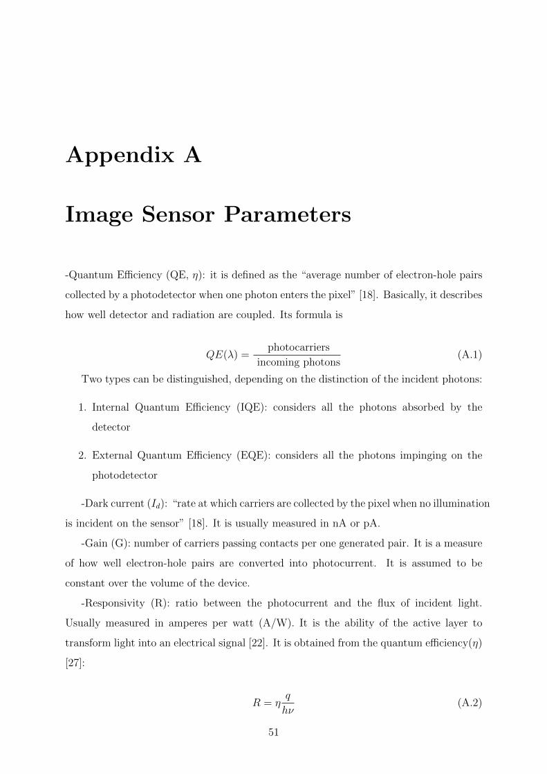
Appendix A
Image Sensor Parameters
-Quantum Efficiency (QE, η): it is defined as the “average number of electron-hole pairs
collected by a photodetector when one photon enters the pixel” [18]. Basically, it describes
how well detector and radiation are coupled. Its formula is
QE(λ) =photocarriers
incoming photons(A.1)
Two types can be distinguished, depending on the distinction of the incident photons:
1. Internal Quantum Efficiency (IQE): considers all the photons absorbed by the
detector
2. External Quantum Efficiency (EQE): considers all the photons impinging on the
photodetector
-Dark current (Id): “rate at which carriers are collected by the pixel when no illumination
is incident on the sensor” [18]. It is usually measured in nA or pA.
-Gain (G): number of carriers passing contacts per one generated pair. It is a measure
of how well electron-hole pairs are converted into photocurrent. It is assumed to be
constant over the volume of the device.
-Responsivity (R): ratio between the photocurrent and the flux of incident light.
Usually measured in amperes per watt (A/W). It is the ability of the active layer to
transform light into an electrical signal [22]. It is obtained from the quantum efficiency(η)
[27]:
R = ηq
hν(A.2)
51

where hν is the incident photon energy and q the charge of the carrier.
-Detectivity (D*): main parameter characterizing normalized to signal noise performance
of detectors; it measures the signal to noise ratio produced by a 1cm2 detector when 1W
of optical power impinges on it, measured with an electrical bandwidth of 1Hz. Its
main advantage is that it allows to compare the performance of detectors with different
sizes and geometries. Values are given in units of cm · Hz1/2W−1 or in jones (1 Jones=1
cm · Hz1/2W−1).
Assuming that the dark current is the main source of noise, Detectivity can be related
to responsivity as follows [8]:
D∗ = RA1/2(2qId)−1/2 (A.3)
where R is the responsivity and A the surface area.
-Temporal photoresponse: time taken to rise to 1− 1/e (τrise) and fall to 1/e (τfall) in
a peak value, after an excitation of the system with light [8]. Also called transient time.
52
Appendix B
Image Sensor Technologies
The two main underlying technologies of image sensors, as it has been pointed in Chapter
3, are CCDs and CMOSs. A brief explanation of their working principles will be provided
here. A more detailed review on this topic may be found in [18].
B.0.1 Charge Coupled Devices (CCDs)
Their operation principle is based on a MOS capacitor (a device designed to store charge).
The voltage on the gate of this capacitor creates a potential well, which can be used to
store charges. In the case of the sensor, by controlling the voltages on each gate of pixel,
a potential profile can be created. Voltage differences also allow to move the charges from
the left to the right, that is, from pixel to pixel. Thus, photocharge is moved from the pixel
where light is “harvested” down to the vertical CCD and then to the horizontal CCD.
From there, photocharge is carried to an output amplifier and the signal is interpreted by
the software.
The main advantage of CCDs is their ability to transport charges almost noisily.
However, to fulfil this characteristic, the transfer process has to be almost perfect. Their
use has decreased to the benefit of CMOSs.
B.0.2 Complementary-Metal-Oxide-Semiconductor (CMOS)
CMOSs image sensors are formed by an array of pixels, row and column decoders, column
amplifiers and output multiplexer. They can be either active or passive pixel sensors.
Almost all the sensors currently designed are based on the active ones, so only the working
53

Figure B.1: Diagram of CCD image sensor [18].
principle of these will be described.
Three different parts can be identified: the storage well (SW), the transfer gate (TG)
and the floating device (FD), an output contact. Signal photocarriers are collected and
stored in SW (QDs in this thesis), while keeping them well isolated from FD by a low
voltage. FD is reset and, by changing the potential of TG, the charge is transferred from
SW to FD, to be afterwards analysed.
Figure B.2: Potential profile, ilustrating the action of the transfer gate (TG) [7].
54
Related Documents