Microelectronic Engineering 51–52 (2000) 99–109 www.elsevier.nl / locate / mee Quantum Coulomb blockade in gate-controlled quantum dots * S. Bednarek, B. Szafran , J. Adamowski ´ Faculty of Physics and Nuclear Techniques, University of Mining and Metallurgy (AGH), Krakow, Poland Abstract A theoretical description is presented for transport–spectroscopy experiments with gate-controlled quantum dots. We have ¨ obtained a self-consistent solution of the Poisson–Schrodinger problem for the quantum-dot nanodevice, calculated the confinement potential, and determined the conditions for the single-electron tunneling, that is closely related with the quantum Coulomb blockade. We have also performed calculations for the gate-controlled quantum dot under an external magnetic field and obtained a very good agreement with the experimental results. 2000 Elsevier Science B.V. All rights reserved. Keywords: Quantum dot; Single-electron transistor; Coulomb blockade; Artificial atom; Transport spectroscopy PACS: 73.20.Dx 1. Introduction Modern nanotechnology enables us to fabricate semiconductor devices of nanometer size [1]. Usually, the main part of the nanodevice consists of a quantum dot [2,3], in which the excess electrons are confined in all three dimensions. The system of confined electrons exhibits atomic-like properties and is called an artificial atom [4–6], since the confinement potential can be tuned by changing the voltage applied to external electrodes. The quantum-dot nanodevice with attached source, drain and gate electrodes is a possible realization of a single-electron transistor [7]. In quantum dots, one can observe single-electron charging and single-electron tunneling phenomena, which provide a basis for capacitance spectroscopy [8] and transport spectroscopy [9]. Single-electron charging and tunneling is usually interpreted in terms of Coulomb-blockade effects [10,11]). The classical model [12] of the Coulomb blockade is based on a charge quantization. 2 According to this model, [12] an amount of energy e / C is required in order to charge the quantum dot of capacitance C by one excess electron, where e is the elementary charge. This model predicts equally spaced tunneling current peaks (Coulomb oscillations). However, in nanometer-sized quantum dots, the three-dimensional confinement potential leads to discrete electron energy levels, which are *Corresponding author. Tel.: 148-12-617-3549; fax: 148-12-634-0010. E-mail address: [email protected] (B. Szafran) 0167-9317 / 00 / $ – see front matter 2000 Elsevier Science B.V. All rights reserved. PII: S0167-9317(99)00472-4

Welcome message from author
This document is posted to help you gain knowledge. Please leave a comment to let me know what you think about it! Share it to your friends and learn new things together.
Transcript
Microelectronic Engineering 51–52 (2000) 99–109www.elsevier.nl / locate /mee
Quantum Coulomb blockade in gate-controlled quantum dots*S. Bednarek, B. Szafran , J. Adamowski
´Faculty of Physics and Nuclear Techniques, University of Mining and Metallurgy (AGH), Krakow, Poland
Abstract
A theoretical description is presented for transport–spectroscopy experiments with gate-controlled quantum dots. We have¨obtained a self-consistent solution of the Poisson–Schrodinger problem for the quantum-dot nanodevice, calculated the
confinement potential, and determined the conditions for the single-electron tunneling, that is closely related with thequantum Coulomb blockade. We have also performed calculations for the gate-controlled quantum dot under an externalmagnetic field and obtained a very good agreement with the experimental results. 2000 Elsevier Science B.V. All rightsreserved.
Keywords: Quantum dot; Single-electron transistor; Coulomb blockade; Artificial atom; Transport spectroscopy
PACS: 73.20.Dx
1. Introduction
Modern nanotechnology enables us to fabricate semiconductor devices of nanometer size [1].Usually, the main part of the nanodevice consists of a quantum dot [2,3], in which the excesselectrons are confined in all three dimensions. The system of confined electrons exhibits atomic-likeproperties and is called an artificial atom [4–6], since the confinement potential can be tuned bychanging the voltage applied to external electrodes. The quantum-dot nanodevice with attachedsource, drain and gate electrodes is a possible realization of a single-electron transistor [7]. Inquantum dots, one can observe single-electron charging and single-electron tunneling phenomena,which provide a basis for capacitance spectroscopy [8] and transport spectroscopy [9].
Single-electron charging and tunneling is usually interpreted in terms of Coulomb-blockade effects[10,11]). The classical model [12] of the Coulomb blockade is based on a charge quantization.
2According to this model, [12] an amount of energy e /C is required in order to charge the quantumdot of capacitance C by one excess electron, where e is the elementary charge. This model predictsequally spaced tunneling current peaks (Coulomb oscillations). However, in nanometer-sized quantumdots, the three-dimensional confinement potential leads to discrete electron energy levels, which are
*Corresponding author. Tel.: 148-12-617-3549; fax: 148-12-634-0010.E-mail address: [email protected] (B. Szafran)
0167-9317/00/$ – see front matter 2000 Elsevier Science B.V. All rights reserved.PI I : S0167-9317( 99 )00472-4
100 S. Bednarek et al. / Microelectronic Engineering 51 –52 (2000) 99 –109
not equally spaced. Therefore, the charging energies are different for different numbers of excesselectrons and the observed Coulomb oscillations [13] exhibit unequal spacings, which is amanifestation of the quantum nature of the Coulomb blockade. The electron–electron Coulombinteraction in many-electron quantum dots quantitatively modifies this picture, but does not change thequantum nature of the Coulomb blockade in semiconductor nanostructures. In few-electron quantumdots, the other quantum phenomena observed [13] result from shell filling in artificial atoms.
The quantum dots have been the subject of many recent experimental [7,8,13–20] and theoretical[21–26] papers. Among the various types of quantum dots, the gate-controlled (gated) quantum dots[8] and self-assembled (self-organized) quantum dots [8] are the most intensively studied. The gatedquantum dots [7,13,14] provide the possibility of tuning the confinement potential by changing thegate voltage and therefore modifying the electronic properties of the nanodevice. In recent years, veryinteresting experimental studies with gated quantum dots have been performed by Tarucha et al. [13]and Kouwenhoven et al. [14]. The nanodevice described in Refs. [7,13] exhibits the properties of thesingle-electron transistor. For the vanishing source–drain voltage, the single-electron transistor is inthe off-state if the chemical potential of electrons confined in the quantum dot differs from the Fermienergy of the source and drain contacts. The off-state corresponds to the quantum Coulomb blockade.The single-electron transistor can be switched into the on-state by applying a voltage to the gate,which changes the energies of the electrons confined in the quantum dot. If the chemical potential ofthe confined electrons and source /drain Fermi levels become adjusted to each other, the quantumblockade is removed and single-electron tunneling occurs. In this case, the sharp peaks of source–drain current are observed [13] even at the very small source–drain voltage. The positions of thecurrent peaks [13] on the gate-voltage scale can be converted into energy, which enables us tomeasure the separations between the energy levels of the artificial atoms, which are formed in thequantum dot, and provides a basis for transport spectroscopy [9]. Unequal spacings between thesource–drain current peaks [13] are interpreted as resulting from the shell filling of the artificialatoms. The same experiment performed in an external magnetic field [13] allows us to tracemagnetic-field induced transformations of the ground state of artificial atoms.
Until recently, the beautiful experiments of Tarucha et al. [13] and Kouwenhoven et al. [14] havebeen interpreted only qualitatively in the frame of the two-dimensional model of the quantum dot[22–26]. The confinement potential was assumed [22–26] to be the two-dimensional harmonic-oscillator, gate-voltage independent, potential. In our quantitative model description [27] of the shellfilling in the gated quantum dot [13], we have applied the three-dimensional anharmonic confinementpotential, which was assumed to be proportional to the gate voltage. In the present paper, we providea comprehensive theory, which accounts for all the observed [13,14] electronic properties of thegate-controlled quantum dots. The present theory is based on a self-consistent solution of the
¨Poisson–Schrodinger problem in the three dimensions. Therefore, the confinement potential is notassumed as in the other papers [22–26], but calculated as a function of gate voltage, geometry of thenanodevice, and donor-impurity distribution. An excellent agreement with the experimental results[13,14] is obtained.
¨2. Solution of Poisson–Schrodinger problem
In the present paper, we have applied the model nanostructure, which possibly well approximatesthe real nanodevice [13] and allows us to perform the calculations with the required precision. The
S. Bednarek et al. / Microelectronic Engineering 51 –52 (2000) 99 –109 101
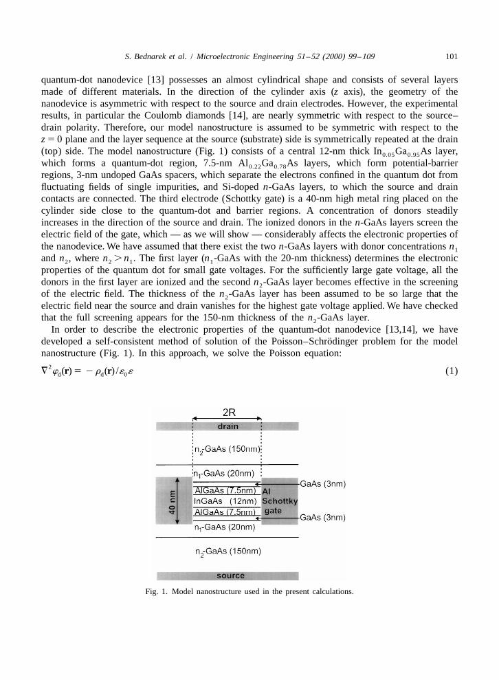
quantum-dot nanodevice [13] possesses an almost cylindrical shape and consists of several layersmade of different materials. In the direction of the cylinder axis (z axis), the geometry of thenanodevice is asymmetric with respect to the source and drain electrodes. However, the experimentalresults, in particular the Coulomb diamonds [14], are nearly symmetric with respect to the source–drain polarity. Therefore, our model nanostructure is assumed to be symmetric with respect to thez 5 0 plane and the layer sequence at the source (substrate) side is symmetrically repeated at the drain(top) side. The model nanostructure (Fig. 1) consists of a central 12-nm thick In Ga As layer,0.05 0.95
which forms a quantum-dot region, 7.5-nm Al Ga As layers, which form potential-barrier0.22 0.78
regions, 3-nm undoped GaAs spacers, which separate the electrons confined in the quantum dot fromfluctuating fields of single impurities, and Si-doped n-GaAs layers, to which the source and draincontacts are connected. The third electrode (Schottky gate) is a 40-nm high metal ring placed on thecylinder side close to the quantum-dot and barrier regions. A concentration of donors steadilyincreases in the direction of the source and drain. The ionized donors in the n-GaAs layers screen theelectric field of the gate, which — as we will show — considerably affects the electronic properties ofthe nanodevice. We have assumed that there exist the two n-GaAs layers with donor concentrations n1
and n , where n . n . The first layer (n -GaAs with the 20-nm thickness) determines the electronic2 2 1 1
properties of the quantum dot for small gate voltages. For the sufficiently large gate voltage, all thedonors in the first layer are ionized and the second n -GaAs layer becomes effective in the screening2
of the electric field. The thickness of the n -GaAs layer has been assumed to be so large that the2
electric field near the source and drain vanishes for the highest gate voltage applied. We have checkedthat the full screening appears for the 150-nm thickness of the n -GaAs layer.2
In order to describe the electronic properties of the quantum-dot nanodevice [13,14], we have¨developed a self-consistent method of solution of the Poisson–Schrodinger problem for the model
nanostructure (Fig. 1). In this approach, we solve the Poisson equation:2
= w (r) 5 2 r (r) /´ ´ (1)d d 0
Fig. 1. Model nanostructure used in the present calculations.
102 S. Bednarek et al. / Microelectronic Engineering 51 –52 (2000) 99 –109
for the potential w (r) created by the external electrodes and ionized donors of the charge densityd
r (r), where ´ is the permittivity of vacuum, and ´ is the static dielectric constant of GaAs. Whend 0
determining charge density r (r) we neglect the thermal ionization of the donors, since thed
experiments [2] were performed at very low temperatures, and assume that the donor at the position rbecomes ionized, if the total potential energy U(r) of the electron is larger than the binding energy Wd
of the electron on the donor center, i.e.:
U(r) . W (2)d
The charge density of ionized donors is determined as follows: r (r) 5 en for these donor positions,d d
for which inequality (2) is satisfied, and r (r) 5 0 otherwise. The donor concentration n is equal to 0,d d
n , and n for the GaAs spacer, n -GaAs, and n -GaAs layers, respectively. The total potential energy1 2 1 2
of the electron:
U(r) 5 2 eF(r) (3)
is determined by the total electrostatic potential F(r) given by:
F(r) 5 w (r) 1 w (r) (4)d e
where potential w (r) stems from the electrons confined in the quantum dot. This potential ise
calculated according to the formula:2N21 uc (r9)ue n3
]] ]]]w (r) 5 2 O E d r9 (5)e 4p´ ´ ur 2 r9u0 n51
where the sum runs over all the occupied one-electron states, whose wave functions c (r) are obtainedn
by the Hartree–Fock method. The upper summation limit corresponds to the N 2 1 electrons bound inthe quantum dot. This is the stationary description of the tunneling of the Nth electron through the dot,which is valid if the probability of finding the tunneling electron inside the dot is much smaller thanthat outside the dot.
In order to solve Poisson equation (1), we need proper boundary conditions. These boundaryconditions can be put on the total potential F, which is connected with the donor impurity potential wd
by Eq. (4). The total potential F essentially depends on the voltages applied to the source, drain andgate electrodes. Therefore, the external voltages affect the potential confining the electrons in the dotvia the boundary conditions. Poisson equation (1) is solved by the finite-difference relaxation methodin the cylindrical coordinates (r, z) on the two-dimensional mesh (r 5 iDr, z 5 jDz). For thisi j
purpose, we consider the finite region: 0 # r # r and 0 # z # z , limited by the metal surfaces,max max
which are supplemented by the cylinder surfaces between the drain and gate (source and drain)electrodes (Fig. 1). Since the source and drain form ohmic contacts with the doped n-GaAs regions,we assume that F(r ) 5V and F(r ) 5V , where V and V are the source and drain voltages,source s drain d s d
respectively. The gate electrode is in contact with the undoped semiconductor; so, we have to takeinto account the Schottky-barrier potential f 50.65 eV, appropriate for the Al–GaAs interface [30].B
This leads to the following boundary condition: F(r ) 5V 2 f , where V is the gate voltage. Wegate g B g
require that the normal derivatives of F vanish on the supplementing surfaces. This boundarycondition is valid for r → `. In the numerical calculations, the radius of the quantum dot has to bemax
finite. We have checked that decreasing r to R5220 nm, which corresponds to the radius of a realmax
nanodevice [13], has a negligible influence on the value of the confinement potential inside the dot.
S. Bednarek et al. / Microelectronic Engineering 51 –52 (2000) 99 –109 103
The present numerical solution of the Poisson equation yields the values w (r , z ) of the potentiald i j
on the two-dimensional mesh. Due to the small thickness of the quantum dot, we use in theHartree–Fock calculations the values of the potential for z50, i.e. w (r, 0). Moreover, since thed
analytical form of the potential is more convenient for solving the Hartree–Fock equations, we havefitted the 2M-order polynomial:
M2m
w̃(r) 5O v r (6)mm50
to the numerical results w (r , 0) obtained from the Poisson equation. We have found that thed i
sixth-order polynomial is necessary for correct reproduction of the numerical solutions.¨The present self-consistent approach is completed by solving the Schrodinger equation for the
N-electron system using the Hartree–Fock method. In the Hartree–Fock equations, we assume thepotential energy of the electron in an external field to be:
˜U (r) 5 U (z) 2 ew(r) (7)ext db
where U (z) is the potential energy of the electron in the double-barrier GaAs–AlGaAs–InGaAsdb
heterostructure given by:
U for InGaAs quantum dotw
U for AlGaAs barriersU (z) 5 (8)bdb 50 for GaAs spacers
where U and U are the energies of the potential well and barrier, respectively. We have solved thew b
Hartree–Fock equations by expanding the one-electron wave functions in the Gaussian basis [27–29]:
c (r) 5O c g (r) (9)n n nn
wherep q 2 2 2n ng (r) 5 x y exp[2a (x 1 y ) 2 b z ] (10)n n n
c , a and b are the variational parameters, p and q are integers, and the number of basis elementsn n n n n
included in Eq. (9) is 45. The one-electron wave functions depend on the external potential (7),which, in turn, is determined by the one-electron wave functions via Eq. (5). Therefore, the present
¨Poisson–Schrodinger problem has to be solved self-consistently.The shape of the real nanodevice can deviate from the ideal cylindrical shape [31]. We have taken
into account this asymmetry by introducing a small anisotropy of the quantum dot into theHartree–Fock equations, which slightly changes the ground-state energy of the N-electron artificialatom and leads to a better agreement with experiments. In the Hartree–Fock equations, we have
2 2 2 2 2˜ ˜replaced variable r in Eq. (6) by r, where r 5 (1 1 g ) x 1 (1 2 g ) y and g is the anisotropyparameter.
For the quantum-dot nanodevice [13], their physical parameters are not given with the requiredprecision or only the nominal donor concentrations are provided. Therefore, in the present work, wehave treated the following parameters: donor concentrations n and n , anisotropy parameter g, and1 2
potential-well depth U , as adjustable parameters. Their actual values, found in the presentw16 23 16 23calculations, are: n 5 6.3 3 10 cm , n 5 17.5 3 10 cm , g 5 0.035, and U 5 2 55 meV.1 2 w
104 S. Bednarek et al. / Microelectronic Engineering 51 –52 (2000) 99 –109
Moreover, we have set the values of the other material parameters, namely, the electron effective bandmass is equal to 0.065 of electron rest mass, ´512.6, and U 5220 meV.b
3. Results and discussion
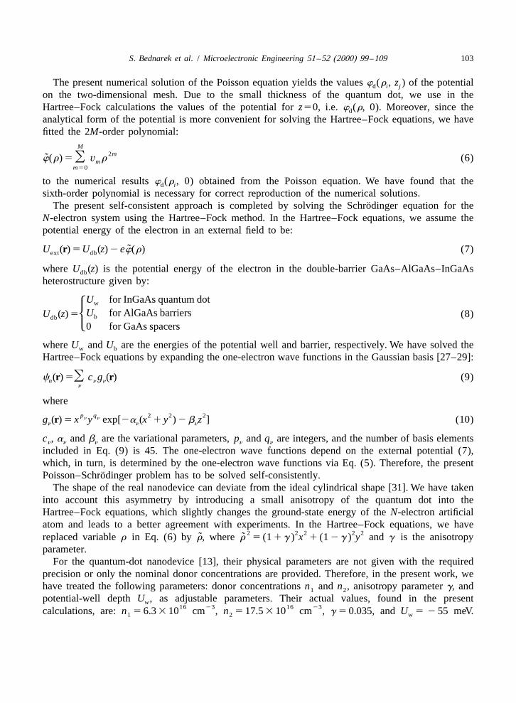
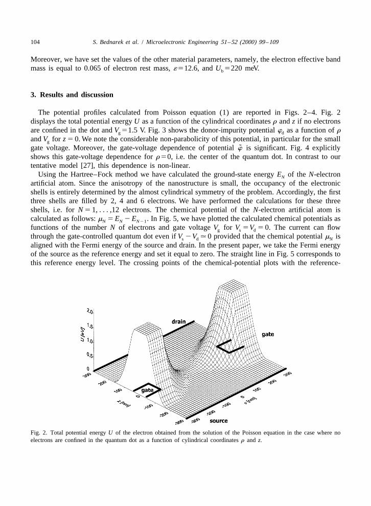
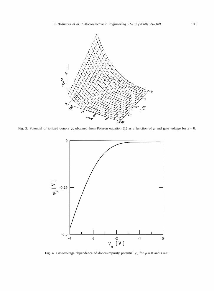
The potential profiles calculated from Poisson equation (1) are reported in Figs. 2–4. Fig. 2displays the total potential energy U as a function of the cylindrical coordinates r and z if no electronsare confined in the dot and V 51.5 V. Fig. 3 shows the donor-impurity potential w as a function of rg d
and V for z 5 0. We note the considerable non-parabolicity of this potential, in particular for the smallg
˜gate voltage. Moreover, the gate-voltage dependence of potential w is significant. Fig. 4 explicitlyshows this gate-voltage dependence for r 50, i.e. the center of the quantum dot. In contrast to ourtentative model [27], this dependence is non-linear.
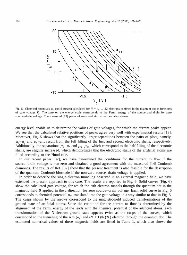
Using the Hartree–Fock method we have calculated the ground-state energy E of the N-electronN
artificial atom. Since the anisotropy of the nanostructure is small, the occupancy of the electronicshells is entirely determined by the almost cylindrical symmetry of the problem. Accordingly, the firstthree shells are filled by 2, 4 and 6 electrons. We have performed the calculations for these threeshells, i.e. for N 5 1, . . . ,12 electrons. The chemical potential of the N-electron artificial atom iscalculated as follows: m 5 E 2 E . In Fig. 5, we have plotted the calculated chemical potentials asN N N21
functions of the number N of electrons and gate voltage V for V 5V 5 0. The current can flowg s d
through the gate-controlled quantum dot even if V 2V . 0 provided that the chemical potential m iss d N
aligned with the Fermi energy of the source and drain. In the present paper, we take the Fermi energyof the source as the reference energy and set it equal to zero. The straight line in Fig. 5 corresponds tothis reference energy level. The crossing points of the chemical-potential plots with the reference-
Fig. 2. Total potential energy U of the electron obtained from the solution of the Poisson equation in the case where noelectrons are confined in the quantum dot as a function of cylindrical coordinates r and z.
S. Bednarek et al. / Microelectronic Engineering 51 –52 (2000) 99 –109 105
Fig. 3. Potential of ionized donors w obtained from Poisson equation (1) as a function of r and gate voltage for z 5 0.d
Fig. 4. Gate-voltage dependence of donor-impurity potential w for r 5 0 and z 5 0.d
106 S. Bednarek et al. / Microelectronic Engineering 51 –52 (2000) 99 –109
Fig. 5. Chemical potentials m (solid curves) calculated for N 5 1, . . . ,12 electrons confined in the quantum dot as functionsN
of gate voltage V . The zero on the energy scale corresponds to the Fermi energy of the source and drain for zerog
source–drain voltage. The measured [13] peaks of source–drain current are also shown.
energy level enable us to determine the values of gate voltages, for which the current peaks appear.We see that the calculated relative positions of peaks agree very well with experimental results [13].Moreover, Fig. 5 shows that the significantly larger separations between the pairs of plots, namely,m –m and m –m , result from the full filling of the first and second electronic shells, respectively.2 3 6 7
Additionally, the separations m –m and m –m , which correspond to the half filling of the electronic4 5 9 10
shells, are slightly increased, which demonstrates that the electronic shells of the artificial atoms arefilled according to the Hund rule.
In our recent paper [32], we have determined the conditions for the current to flow if thesource–drain voltage is non-zero and obtained a good agreement with the measured [14] Coulombdiamonds. The results of Ref. [32] show that the present treatment is also feasible for the descriptionof the quantum Coulomb blockade if the non-zero source–drain voltage is applied.
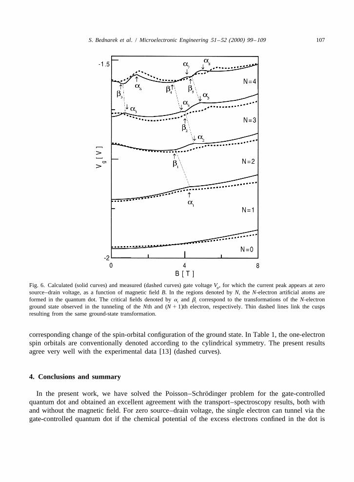
In order to describe the single-electron tunneling observed in an external magnetic field, we haveextended the present approach to this case. The results are reported in Fig. 6. Solid curves (Fig. 6)show the calculated gate voltage, for which the Nth electron tunnels through the quantum dot in themagnetic field B applied in the z direction for zero source–drain voltage. Each solid curve in Fig. 6corresponds to chemical potential m , translated into the gate voltage in a way similar to that in Fig. 5.N
The cusps shown by the arrows correspond to the magnetic-field induced transformations of theground state of artificial atoms. Since the condition for the current to flow is determined by thealignment of the Fermi energy of the leads with the chemical potential of the artificial atoms, eachtransformation of the N-electron ground state appears twice as the cusps of the curves, whichcorrespond to the tunneling of the Nth (a ) and (N 1 1)th (b ) electron through the quantum dot. Thei i
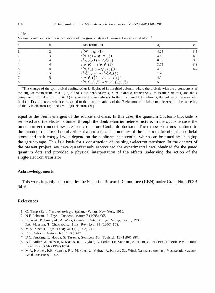
estimated numerical values of these magnetic fields are listed in Table 1, which also shows the
S. Bednarek et al. / Microelectronic Engineering 51 –52 (2000) 99 –109 107
Fig. 6. Calculated (solid curves) and measured (dashed curves) gate voltage V , for which the current peak appears at zerog
source–drain voltage, as a function of magnetic field B. In the regions denoted by N, the N-electron artificial atoms areformed in the quantum dot. The critical fields denoted by a and b correspond to the transformations of the N-electroni i
ground state observed in the tunneling of the Nth and (N 1 1)th electron, respectively. Thin dashed lines link the cuspsresulting from the same ground-state transformation.
corresponding change of the spin-orbital configuration of the ground state. In Table 1, the one-electronspin orbitals are conventionally denoted according to the cylindrical symmetry. The present resultsagree very well with the experimental data [13] (dashed curves).
4. Conclusions and summary
¨In the present work, we have solved the Poisson–Schrodinger problem for the gate-controlledquantum dot and obtained an excellent agreement with the transport–spectroscopy results, both withand without the magnetic field. For zero source–drain voltage, the single electron can tunnel via thegate-controlled quantum dot if the chemical potential of the excess electrons confined in the dot is
108 S. Bednarek et al. / Microelectronic Engineering 51 –52 (2000) 99 –109
Table 1aMagnetic-field induced transformations of the ground state of few-electron artificial atoms
i N Transformation a bi i
21 2 s (0) → sp (1) 4.25 3.522 1 3
] ]2 3 s p ( ) → sp d ( ) 4.5 42 2 22 22 2 23 4 s p p (1) → s p (0) 0.75 0.52 1 22 2 24 4 s p (0) → s p d (1) 3.75 3.32 2 225 4 s p d (1) → sp d f (2) 4.9 4.42 2 2 2 22 2 2 21 1
] ]6 5 s p p ( ) → s p d ( ) 1.42 1 2 22 22 2 21 3
] ]7 5 s p d ( ) → s p d f ( ) 4.12 2 2 2 22 22 3 5
] ]8 5 s p d f ( ) → sp d f g ( ) 52 2 2 2 2 2 22 2
a The change of the spin-orbital configuration is displayed in the third column, where the orbitals with the z component ofthe angular momentum l50, 1, 2, 3 and 4 are denoted by s, p, d, f and g, respectively, 6 is the sign of l, and the zcomponent of total spin (in units ") is given in the parentheses. In the fourth and fifth columns, the values of the magneticfield (in T) are quoted, which correspond to the transformations of the N-electron artificial atoms observed in the tunnelingof the Nth electron (a ) and (N 1 1)th electron (b ).i i
equal to the Fermi energies of the source and drain. In this case, the quantum Coulomb blockade isremoved and the electrons tunnel through the double-barrier heterostructure. In the opposite case, thetunnel current cannot flow due to the quantum Coulomb blockade. The excess electrons confined inthe quantum dot form bound artificial-atom states. The number of the electrons forming the artificialatoms and their energy levels depend on the confinement potential, which can be tuned by changingthe gate voltage. This is a basis for a construction of the single-electron transistor. In the context ofthe present project, we have quantitatively reproduced the experimental data obtained for the gatedquantum dots and provided a physical interpretation of the effects underlying the action of thesingle-electron transistor.
Acknowledgements
This work is partly supported by the Scientific Research Committee (KBN) under Grant No. 2P03B3416.
References
[1] G. Timp (Ed.), Nanotechnology, Springer Verlag, New York, 1999.[2] N.F. Johnson, J. Phys.: Condens. Matter 7 (1995) 965.
´[3] L. Jacak, P. Hawrylak, A. Wojs, Quantum Dots, Springer Verlag, Berlin, 1998.[4] P.A. Maksym, T. Chakraborty, Phys. Rev. Lett. 65 (1990) 108.[5] M.A. Kastner, Phys. Today 46 (1) (1993) 24.[6] R.C. Ashoori, Nature 379 (1996) 413.[7] D.G. Austing, T. Honda, S. Tarucha, Semicon. Sci. Technol. 11 (1996) 388.[8] B.T. Miller, W. Hansen, S. Manus, R.J. Luyken, A. Lorke, J.P. Kotthaus, S. Huant, G. Medeiros-Ribeiro, P.M. Petroff,
Phys. Rev. B 56 (1997) 6764.[9] M.A. Kastner, E.B. Foxman, P.L. McEuen, U. Meirav, A. Kumar, S.J. Wind, Nanostructures and Mesoscopic Systems,
Academic Press, 1992.
S. Bednarek et al. / Microelectronic Engineering 51 –52 (2000) 99 –109 109
[10] D.V. Averin, A.N. Korotkov, K.K. Likharev, Phys. Rev. B 44 (1991) 6199.[11] C.W.J. Beenakker, H. van Houten, A.A.M. Staring, Phys. Rev. B 44 (1991) 1657.[12] L.P. Kouwenhoven, N.C. van der Vaart, A.T. Johnson, W. Kool, C.J.P.M. Harmans, J.G. Williamson, A.A.M. Staring,
C.D. Foxon, Z. Phys. B: Condens. Matter 85 (1991) 367.[13] S. Tarucha, D.G. Austing, T. Honda, R.J. van der Hage, L.P. Kouwenhoven, Phys. Rev. Lett. 77 (1996) 3613.[14] L.P. Kouwenhoven, T.H. Oosterkamp, M.W.S. Danoesastro, M. Eto, D.G. Austing, T. Honda, S. Tarucha, Science 278
(1997) 1788.[15] M. Grundmann, O. Stier, D. Bimberg, Phys. Rev. B 52 (1995) 11969.
¨ ¨[16] T. Schmidt, M. Tewordt, R.H. Blick, R.J. Haug, D. Pfannkuche, K. von Klitzing, A. Forster, H. Luth, Phys. Rev. B 51(1995) 5570.
[17] J.L. Merz, S. Lee, J.K. Furdyna, J. Cryst. Growth 184–185 (1998) 228.[18] M. Hirasawa, S. Katsumoto, A. Endo, Y. Iye, Physica B 249–251 (1998) 252.
¨[19] S.R. Patel, S.M. Cronenwett, D.R. Stewart, A.G. Huibers, C.M. Marcus, C.I. Duruoz, J.S. Harris Jr., K. Campman, A.C.Gossard, Phys. Rev. Lett. 20 (1998) 4522.
[20] D. Berman, N.B. Zhitenev, R.C. Ashoori, M. Shayegan, Phys. Rev. Lett. 82 (1999) 161.[21] A. Wojs, P. Hawrylak, S. Fafard, L. Jacak, Phys. Rev. B 54 (1996) 5604.[22] M. Koskinen, M. Manninen, S.M. Reimann, Phys. Rev. Lett. 79 (1997) 1389.[23] M. Eto, Jpn. J. Appl. Phys. 36 (1997) 3924.[24] S. Nagaraja, P. Matagne, V.-Y. Thean, J.-P. Leburton, Y.-H. Kim, R.M. Martin, Phys. Rev. B. 56 (1997) 15752.[25] H. Tamura, Physica B 249–251 (1998) 210.
¨[26] O. Steffens, M. Suhrke, U. Rossler, Physica B 256–258 (1998) 147.[27] B. Szafran, S. Bednarek, J. Adamowski, Acta Phys. Pol. A 94 (1998) 555.
´ ´[28] J. Adamowski, B. Szafran, S. Bednarek, B. Stebe, Few-Body Systems Suppl. 10 (1999) 189.[29] S. Bednarek, B. Szafran, J. Adamowski, Phys. Rev. B 59 (1999) 13036.[30] R.J. Luyken, A. Lorke, M. Haslinger, B.T. Miller, M. Fricke, J.P. Kotthaus, G. Medeiros-Ribeiro, P.M. Petroff, Physica
E 2 (1998) 704.[31] M. Eto, J. Phys. Soc. Jpn. 66 (1997) 2244.[32] S. Bednarek, B. Szafran, J. Adamowski, Thin Solid Films, in press.
Related Documents