Quantitative Phase Imaging of Magnetic Nanostructures Using Off-Axis Electron Holography by Kai He A Dissertation Presented in Partial Fulfillment of the Requirements for the Degree Doctor of Philosophy Approved November 2010 by the Graduate Supervisory Committee: Martha R. McCartney, Co-Chair David J. Smith, Co-Chair Ralph V. Chamberlin Peter A. Crozier Jeff Drucker ARIZONA STATE UNIVERSITY December 2010

Welcome message from author
This document is posted to help you gain knowledge. Please leave a comment to let me know what you think about it! Share it to your friends and learn new things together.
Transcript

Quantitative Phase Imaging of Magnetic Nanostructures
Using Off-Axis Electron Holography
by
Kai He
A Dissertation Presented in Partial Fulfillment of the Requirements for the Degree
Doctor of Philosophy
Approved November 2010 by the Graduate Supervisory Committee:
Martha R. McCartney, Co-Chair
David J. Smith, Co-Chair Ralph V. Chamberlin
Peter A. Crozier Jeff Drucker
ARIZONA STATE UNIVERSITY
December 2010
ABSTRACT
The research of this dissertation has involved the nanoscale quantitative
characterization of patterned magnetic nanostructures and devices using off-axis electron
holography and Lorentz microscopy. The investigation focused on different materials of
interest, including monolayer Co nanorings, multilayer Co/Cu/Py (Permalloy, Ni81Fe19)
spin-valve nanorings, and notched Py nanowires, which were fabricated via a standard
electron-beam lithography (EBL) and lift-off process.
Magnetization configurations and reversal processes of Co nanorings, with and
without slots, were observed. Vortex-controlled switching behavior with stepped
hysteresis loops was identified, with clearly defined onion states, vortex states, flux-
closure (FC) states, and Ω states. Two distinct switching mechanisms for the slotted
nanorings, depending on applied field directions relative to the slot orientations, were
attributed to the vortex chirality and shape anisotropy. Micromagnetic simulations were
in good agreement with electron holography observations of the Co nanorings, also
confirming the switching field of 700–800 Oe.
Co/Cu/Py spin-valve slotted nanorings exhibited different remanent states and
switching behavior as a function of the different directions of the applied field relative to
the slots. At remanent state, the magnetizations of Co and Py layers were preferentially
aligned in antiparallel coupled configuration, with predominant configurations in FC or
onion states. Two-step and three-step hysteresis loops were quantitatively determined for
nanorings with slots perpendicular, or parallel to the applied field direction, respectively,
due to the intrinsic coercivity difference and interlayer magnetic coupling between Co
and Py layers. The field to reverse both layers was on the order of ~800 Oe.
Domain-wall (DW) motion within Py nanowires (NWs) driven by an in situ
magnetic field was visualized and quantified. Different aspects of DW behavior,
i
including nucleation, injection, pinning, depinning, relaxation, and annihilation, occurred
depending on applied field strength. A unique asymmetrical DW pinning behavior was
recognized, depending on DW chirality relative to the sense of rotation around the notch.
The transverse DWs relaxed into vortex DWs, followed by annihilation in a reversed
field, which was in agreement with micromagnetic simulations.
Overall, the success of these studies demonstrated the capability of off-axis
electron holography to provide valuable insights for understanding magnetic behavior on
the nanoscale.
ii

This dissertation is dedicated to my parents,
who made everything possible.
iii
ACKNOWLEDGMENTS
I would like to express most sincere thanks to my advisors Professor Martha R.
McCartney and Regents’ Professor David J. Smith for their esteemed support and
guidance that made everything I achieved toward my PhD degree possible. Their open
minds, unlimited enthusiasm, precise insights and meticulous attitudes towards doing
research have educated me with good characteristics and discipline necessary for my
future career. I would also like to thank my dissertation committee members, Professors
Ralph Chamberlin, Peter Crozier, and Jeff Drucker, for their generous time and helpful
suggestions.
I would like to acknowledge the faculty and staff members as well as the use of
facilities in the John M. Cowley Center for High Resolution Electron Microscopy
(CHREM) and the Center for Solid State Electronics Research (CSSER) at Arizona State
University. Special thanks are due to Karl Weiss and Grant Baumgardner in CHREM,
and to Dr. Stefan Myhajlenko and Arthur Handugan in CSSER, for their technical
support and assistance throughout my research. The financial support from US
Department of Energy (Grant No. DE-FG02-04ER46168) is gratefully acknowledged.
I appreciate our collaborators Prof. J. Cumings (University of Maryland) and Dr.
J. Shaw (NIST) who provided samples, expertise, and personal concerns during my PhD
research. I also thank my colleagues at ASU, especially Dr. Hua Wang for training me on
cleanroom facilities, and Samuel Tobler for coating TEM samples.
Particular thanks and best wishes go to all the group members — Dr. Lin Zhou,
Dr. Nipun Agarwal, Dr. Changzhen Wang, Dr. Titus Leo, Dr. M.G. Han, Dr. Suk Chung,
Dr. David Cullen, Luying Li, Lu Ouyang, Wenfeng Zhao, Michael Johnson, Allison
Boley, Sahar Hihath, Jae Jin Kim, Aram Rezikya, Dinghao Tang, Dexin Kong, and et al.
for their friendship and kindness. My experiences with the “M&D Gang” have brought
iv

me a lot of joyful memories.
I appreciate the China Scholarship Council and the Ministry of Education for
awarding me the prestigious “Chinese Government Award for Outstanding Self-Financed
Students Abroad” towards my achievements during the Ph.D. studies. This recognition
from my mother country is the highest honor to inspire me heading forward.
Last but not least, I express the most heartfelt gratitude to my family, for their
infinite love and support that I could never pay back.
v

TABLE OF CONTENTS
Page
LIST OF TABLES............................................................................................................. ix
LIST OF FIGURES ............................................................................................................ x
CHAPTER
1. INTRODUCTION ................................................................................................. 1
1.1. Background .................................................................................................. 1
1.1.1. Fundamentals of magnetism............................................................... 1
1.1.2. Development of magnetic storage...................................................... 4
1.2. Nanopatterned Magnetic Recording Media ................................................. 6
1.2.1. Fabrication.......................................................................................... 7
1.2.2. Characterization ............................................................................... 12
1.2.3. Magnetic properties.......................................................................... 15
1.2.4. Advances and challenges ................................................................. 22
1.3. Magnetic Domain Wall and Related Devices ............................................ 23
1.3.1. Racetrack memory............................................................................ 23
1.3.2. Domain-wall logic............................................................................ 25
1.3.3. Research progress and challenges .................................................... 27
1.4. Outline of Dissertation ............................................................................... 28
References............................................................................................................ 30
2. EXPERIMENTAL DETAILS ............................................................................. 35
2.1. Instrumentation .......................................................................................... 35
2.1.1. Electron beam lithography ............................................................... 35
2.1.2. Transmission electron microscopy................................................... 37
2.2. Fabrication ................................................................................................. 38
vi

CHAPTER Page
2.3. Micromagnetic Simulations ....................................................................... 42
2.4. Characterization ......................................................................................... 44
2.4.1. Lorentz microscopy.......................................................................... 44
2.4.2. Off-axis electron holography............................................................ 46
2.5. Examples of Quantitative Phase Imaging .................................................. 55
2.5.1. Kagome lattices ................................................................................ 55
2.5.2. Ferromagnetic triangles.................................................................... 61
References............................................................................................................ 64
3. MAGNETIZATION CONFIGURATIONS AND VORTEX-CONTROLLED
SWTICHING BEHAVIOR OF Co NANORINGS ............................................. 66
3.1. Introduction................................................................................................ 66
3.2. Remanent States and Switching Behavior of Co Nanorings...................... 69
3.3. Remanent States and Switching Behavior of Slotted Co Nanorings.......... 72
3.4. Comparison Between Experimental Results and Simulations ................... 78
3.5. Discussion .................................................................................................. 83
3.5.1. Effects of vortex chirality on switching mechanisms....................... 83
3.5.2. Effects of shape anisotropy on switching fields ............................... 84
3.6. Conclusions................................................................................................ 86
References............................................................................................................ 87
4. MAGNETIZATION CONFIGURATIONS AND SWTICHING BEHAVIOR
OF Co/Cu/Py SPIN-VALVE SLOTTED NANORINGS.................................... 89
4.1. Introduction................................................................................................ 89
4.2. Magnetization Configurations and Interlayer Coupling at Remanent
State............................................................................................................ 91
vii

CHAPTER Page
4.3. Switching Behavior of Slotted Nanorings.................................................. 95
4.3.1. Applied field perpendicular to slot direction.................................... 95
4.3.2. Applied field parallel to slot direction.............................................. 98
4.4. Conclusions.............................................................................................. 102
References.......................................................................................................... 103
5. MAGNETIC DOMAIN-WALL MOTION IN NOTCHED PERMALLOY
NANOWIRES ................................................................................................... 104
5.1. Introduction.............................................................................................. 104
5.2. Remanent States ....................................................................................... 106
5.3. Asymmetrical Domain-Wall Pinning Behavior ....................................... 108
5.4. Domain Wall Relaxation and Annihilation.............................................. 113
5.5. Discussion ................................................................................................ 118
5.6. Conclusions.............................................................................................. 120
References.......................................................................................................... 122
6. SUMMARY AND FUTURE WORK ............................................................... 124
6.1. Summary .................................................................................................. 124
6.2. Future Work ............................................................................................. 126
6.2.1. Electron holography of nanomagnet arrays.................................... 126
6.2.2. Current-induced DW motion.......................................................... 127
APPENDIX RELEVANT PUBLICATIONS ........................................................... 129
viii

LIST OF TABLES
Table Page
2.1. Essential parameters used for practical micromagnetic simulations. ............... 43
3.1. Switching fields measured from experimental and simulated hysteresis
loops. ................................................................................................................ 78
ix

LIST OF FIGURES
Figure Page
1.1. Typical hysteresis loop of a ferromagnetic material........................................... 2
1.2. Schematic of DW structures and domain configurations. (a) Bloch
wall; (b) Néel wall; (c) – (f) domain configurations, where closure
domain (f) has lowest energy.............................................................................. 4
1.3. Road map of magnetic recording technology [10]. ............................................ 5
1.4. Schematic of: (a) conventional longitudinal thin film media; (b)
patterned media with in-plane magnetization; and (c) patterned media
with perpendicular magnetization [11]. .............................................................. 6
1.5. Schematic of procedures for fabricating patterned media: (a) patterning
followed by electrodeposition; (b) patterning followed by evaporation;
(c) deposition followed by patterning through etch mask. The trilayer.............. 8
1.6. Typical images of nanopatterned element arrays using EBL technique............. 9
1.7. TEM cross-sectional view of Co nanowires and nanoparticles array, as
well as corresponding length distribution and microstructures [56]................. 10
1.8. TEM images showing monodispersed FePt nanoparticle arrays [57]. ............. 11
1.9 Schematic diagram of MOKE magnetometer apparatus [62]........................... 13
1.10. Schematic diagram showing principle of MFM. .............................................. 14
1.11. Schematic diagram showing the principle of SEMPA [68].............................. 15
1.12. Experimentally determined phase diagram showing different magnetic
reversal mechanisms in terms of () vortex, or () single domain
behavior [73]. ................................................................................................... 17
1.13. Electron holographic phase images of magnetic elements with shape of
triangle, square, pentagon, and hexagon, indicating twisted magnetization
x

Figure Page
patterns at remanent state [49]. ......................................................................... 18
1.14. Electron holographic phase images of magnetic elements with different
magnetization patterns at remanent state: (a) disk with “S”-state; (b)
disk with FC state; (c) ring with “Onion” state; (d) slotted-ring with FC ........ 19
1.15. MFM images of elliptical Permalloy elements with aspect ratios
varying from 2 to 10 at the remanent state: (a) 23 nm in thickness after
saturation to the right, and (b) 42 nm in thickness after saturation to the......... 20
1.16. Schematic showing the effect of dipole interaction between two
magnetic particles [61]. .................................................................................... 21
1.17. Schematic showing principle of racetrack memory using pulse-
triggered DW motion along magnetic NWs [75].............................................. 24
1.18. Summary of conventional CMOS circuit elements and corresponding
DW logic elements to realize different logic functionalities [79]..................... 26
1.19. Examples of typical studies on racetrack memory and DW logic [76, 79] ...... 27
2.1. Electron optics system of JBX-6000FS/E [1]................................................... 36
2.2. Schematic for a TEM and its electron optics scheme....................................... 37
2.3. Schematics showing the geometry and dimensions of the membrane
samples: (a) top view; (b) side view. (c) Actual image. ................................... 39
2.4. Schematic outline of EBL process: (a) cleaning membrane; (b)
spinning and baking PMMA; (c) EBL exposure; (d) resist
development; (e) deposition of magnetic material; (f) lift off. ......................... 40
2.5. Schematic of (a) Lorentz force, and (b) Fresnel Lorentz imaging.
Electrons passing through the magnetic sample are deflected due to the
in-plane magnetic field, and form DW magnetic contrast at under- or ............ 45
xi

Figure Page
2.6. Schematic illustrating the typical configuration used for off-axis
electron holography in the TEM (Philips CM200-FEG) [14]. ......................... 46
2.7. Schematic illustration contrasting the origin of phase shifts for
holography of electrostatic and magnetic fields [14]........................................ 48
2.8. Image reconstruction process for extracting phase shifts from hologram ........ 51
2.9. Different representation schemes for phase shifts related to magnetic
field. (a) Pseudo-color phase image; (b) 8× amplified phase contours;
(c) x- and (d) y-gradient of phase in (a); (e) magnetic induction map.............. 51
2.10. (a) Schematic diagram showing the use of specimen tilt to provide the
in-plane component of the applied field needed for in situ
magnetization reversal experiments. (b) Hall probe measurements of............. 54
2.11. (a) In-focus, and (b) defocused, Lorentz TEM image of kagome
structure. Fresnel contrast indicates clockwise and counterclockwise
closed loops. [27].............................................................................................. 55
2.12. Phase images of kagome lattice composed of Py and corresponding
line profiles in remanent state with: (a) saturation field pointing to
bottom-left; (b) saturation field pointing to top-right; and (c) pure.................. 57
2.13. Phase contour map (12× amplified), magnetic induction map, and
magnetic contour map of (a)–(c) 500-nm-diagonal kagome lattice, and
(d)–(f) enlarged box area, respectively. Magnetization directions ................... 59
2.14. (a) Lorentz TEM image of as-fabricated Y-junctions. (b) Hologram of
an individual Y-junction in boxed area of (a). (c) Phase contour map
(12× amplified), (d) magnetic induction map, and (e) magnetic contour......... 60
2.15. Micromagnetic simulations showing remanent configuration: (a) Y state
xii
Figure Page
in a sharp triangle; and (b), (c) buckle states in rounded triangles [29]............ 61
2.16. Lorentz images of Py triangles with different sizes, and corresponding
phase contours (4× amplified) as function of in-plane applied field.
Applied field along the long axis of the triangles............................................. 63
3.1. Schematics showing the geometry of Co nanoring and slotted Co
nanoring, grown on thin silicon nitride TEM membranes: (a) Side
view; and plan view of (b) nanoring; and (c) slotted nanoring......................... 68
3.2. (a) Lorentz TEM image showing Co nanoring array (Scale bar
indicates 500 nm). (b) Reconstructed holographic phase image of an
individual nanoring showing FC state at remanence, with phase..................... 69
3.3. Hysteresis loop of an individual Co nanoring where a–d correspond to
specific states visible in phase images: (a) onion state at saturation; (b)
excitation of double-vortex; (c) FC state; (d) onion state at reverse................. 71
3.4. Lorentz images of Co slotted nanorings, with slot directions (a)
parallel, and (b) perpendicular, to applied field directions (indicated by
double arrow). Reconstructed phase images showing individual Co ............... 73
3.5. (a) Three-step, and (b) one-step, hysteresis loops for Co elements with
applied field parallel, and perpendicular, to the slot direction,
respectively. The inset schematics indicate the different magnetization.......... 75
3.6. Phase images of Co nanoring (SR1) illustrating the magnetization
configurations for corresponding states in the hysteresis loop in 3.5 (a):
(a) onion state; (b) excitation of vortex at remanence; (c) FC state; and.......... 76
3.7. Phase images of Co nanoring (SR2) illustrating the magnetization
configurations for corresponding states in the hysteresis loop shown in
xiii

Figure Page
Figure 3.5 (b): (a) Ω state; (b) FC state of CW; (c) FC state of CCW; ............ 76
3.8. (a)–(c) Experimental, and (d)–(f) simulated, hysteresis loops for Co
nanoring, slotted nanoring with applied field parallel to slot (SR1), and
slotted nanoring with applied field perpendicular to slot (SR2)....................... 79
3.9. Magnetic induction maps for (1) Co ring, (2) SR1, and (3) SR2,
comparing the experimental results (upper row) and simulations (lower
row). Letter labels refer to corresponding states in Figure 3.8. Applied .......... 81
3.10. Schematics showing vortex controlled switching mechanism for
nanorings: (a) vortex motion rule; (b) onion-FC-onion transition; and
(c) coherent onion rotation. .............................................................................. 84
3.11. Demagnetization energy as a function of applied field for Co nanoring
and SR1 shape, as calculated from OOMMF simulations. The
calculation is obtained from the forward hysteresis half-cycle. ....................... 85
4.1. Schematics illustrating (a) the structure of trilayer stack, and (b) the
shape of slotted ring, for Co/Cu/Py SV elements. ............................................ 91
4.2. (a) In-focus image showing as-prepared array of Co/Cu/Py SV
elements (OD/ID= 400/200nm, α = 60°); (b) defocused Fresnel image
of single Co/Cu/Py SV element in remanent state............................................ 92
4.3. Reconstructed holographic phase images of Co/Cu/Py SV elements
showing different remanent configurations: (a) onion state; (b) FC state.
Initial saturation direction from bottom-left to top-right. Color bar................. 93
4.4. Phase images of (a) parallel- and (b) antiparallel-coupled configurations
of slotted SV element at remanent state. (c) Corresponding line profiles
after removal of MIP contributions. ................................................................. 94
xiv

Figure Page
4.5 Hysteresis loops for Co/Cu/Py SV element through major and minor
cycles. Applied field perpendicular to the slot direction. Insert
schematics indicate different magnetic coupling between Co and Py.............. 96
4.6. Phase contour (4× amplified) images showing representative
magnetization states corresponding to labels a–c in Figure 4.7: (a)
parallel coupled Ω-state; (b) parallel coupled FC; (c) antiparallel ................... 97
4.7. Three-step hysteresis loops for Co/Cu/Py SV nanoring with applied
magnetic field parallel to the slot direction. Insert schematics indicate
different magnetic coupling between Co and Py layers with onion ................. 98
4.8. Phase contour (4× amplified) images of SV element illustrating the
magnetization configurations of corresponding states in the hysteresis
loop of Figure 4.7. Applied fields are parallel to the slot direction, ............... 100
4.9. (a) Schematic hysteresis loop after Figure 4.7. Magnetic components
separated to represent the individual behavior of (b) Co, and (c) Py
layers............................................................................................................... 101
5.1. Schematic drawings showing the design of Py NWs: (a) plan-view
showing shape and dimensions; (b) 3D view showing Py NW on the
amorphous nitride membrane. ........................................................................ 106
5.2. (a) Lorentz image of Py nanowire as fabricated, with inset showing
enlarged view of trapezoid notch. (b) Phase shift; (c) reconstructed
magnetic induction map; and (d) calculated magnetic induction map; of ...... 107
5.3. Montage showing representative states during DW motion indicated in
Fresnel images (top) and corresponding magnetic induction maps
(bottom), as extracted from pairs of holograms. (I) DW nucleation, (II) ....... 110
xv

Figure Page
5.4. (a) Schematics of representative configurations, corresponding to states
I − VII in Figure 5.3, respectively. (b) Simulated hysteresis loop
showing extra plateau labeled III due to asymmetrical DW pinning ............. 112
5.5. Defocused Fresnel images showing (a) TDW pinning at the notch with
applied field (H) of ~72 Oe, and (b) relaxation of VDW at remanent
state................................................................................................................. 113
5.6. (a) Experimental, and (b) simulated, magnetic induction maps for DW
pinning state. (c) Experimental, and (d) simulated, magnetic induction
maps of VDW obtained after NW relaxation in zero field. ............................ 114
5.7. (a) Defocused Fresnel images showing representative states during
DW annihilation: (I) DW pinning at the notch; (II) DW depinning from
the notch; (III) two DWs attracting each other; (IV) DW annihilation.. ........ 116
5.8. (a) Schematics of representative configurations, corresponding to states
I − IV in Figure 5.7, respectively. (b) Distribution of critical fields
needed to emerge specific well-defined states (I, II, and IV) during DW ...... 117
5.9. Schematic diagram illustrating the entire process and representative
stages during DW propagation, also indicating correlation between
chiralities of the nucleation pad, DWs, and notch. ......................................... 119
6.1. SEM images showing (a) overview, and (b) enlarged view, of Py NW
with integrated testing electrodes. (c) TEM images showing a notched
Py NW attached to two electrodes.................................................................. 128
6.2. Schematics showing: (a) Py NWs with electrodes integrated on a
silicon nitride membrane window; (b) in situ biasing TEM specimen
holder having a special 2-point contact cartridge to load the membrane ....... 128
xvi

CHAPTER 1
INTRODUCTION
1.1. Background
1.1.1. Fundamentals of magnetism
Magnetism has been a subject of much interest for thousands of years. As early
as 600 BC, magnets were discovered by Greek philosophers, and they were used as
compasses by the Chinese in 400 BC. However, it was not until the 1800s that magnetism
was considered as a scientific discipline, when the relationship between electricity and
magnetism was proposed by Oersted [1]. Nowadays, the principles of magnetism are well
established, and the fundamental concepts [2-4] can be summarized, as found below.
Materials behave differently when they are exposed to an external magnetic field.
In the classical point of view, the basic parameters are magnetic field strength (H),
magnetization (M), and magnetic induction (or magnetic flux density, B), where
magnetization is a measure of material response to applied field, and magnetic induction
is net magnetic flux density inside the material. The relationships between these
parameters are described by the following equations:
HM χ= (1.1)
)(0 HMB += μ (SI units); or HMB π4+= (cgs units) (1.2)
According to their different response (so-called susceptibility χ) to an applied magnetic
field, materials are classified as diamagnetic, paramagnetic, ferromagnetic,
antiferromagnetic, and ferrimagnetic.
Our particular interest here is in ferromagnetic materials, such as iron, cobalt,
nickel, and their alloys. The magnetic moments in ferromagnetic materials are
1

spontaneously aligned in a regular manner, resulting in strong net magnetization even
without any applied field. Ferromagnetic materials have the property of hysteresis, which
can be technically characterized by a hysteresis loop, plotting out magnetization M (or
magnetic induction B) versus applied field H. Figure 1.1 shows a typical hysteresis loop
of a ferromagnetic material. The ferromagnet is initially not magnetized, and application
of the field H causes magnetic induction to increase in the field direction. If H is
increased indefinitely the magnetization eventually reaches saturation at a value which is
designated as Ms. When the external field is reduced to zero, the remaining magnetic
induction is called the remanent magnetization Mr. The magnetic induction can be
reduced to zero by applying a reverse magnetic field of strength Hc, which is known as
the coercivity.
Figure 1.1. Typical hysteresis loop of a ferromagnetic material.
2

The shape of a hysteresis loop reflects the properties of the ferromagnet. The area
inside the hysteresis is proportional to the energy needed to rotate the magnetic moments.
Based on the strength of the coercive field, ferromagnets can be roughly defined as hard
or soft magnetic materials. Hard (or permanent) magnets have coercivity as high as 2×10⁶
A/m (or 25000 Oe), and are widely used in electric motors, generators, loudspeakers,
frictionless bearings, magnetic levitation systems, and various forms of holding magnets
such as door catches. Soft magnets have much lower coercivity such as 1.0 A/m (or 12
mOe), and are mainly used in transformers, inductors, and magnetic sensors. Between
these two extremes are magnetic recording media, which require medium coercivity
(typically ranging from 104 A/m to 105 A/m), high Mr/Ms ratio, and good squareness of
hysteresis loop so as to ensure a sharp binary transition with low noise.
Two additional important concepts important for understanding the behavior of
magnetic materials are magnetic domains and domain walls (DWs). A magnetic domain
describes a region within a material which has uniform magnetization. The regions
separating magnetic domains are called DWs where the direction of the magnetization
rotates, usually coherently, from one domain to the adjacent domain [5]. The existence of
domains is a consequence of energy minimization [6]. Figure 1.2 shows schematics that
illustrate DW structures and domain configurations. To reduce the magnetostatic (MS)
energy, the spins inside the Bloch wall rotate through the plane of the wall, unlike the
Néel wall where the spins rotate in the plane of the wall. As shown in Figure 1.2 (c) – (f),
the introduction of 180° DWs reduces the MS energy but raises the DW energy, whereas
90° closure DWs can eliminate MS energy but increase the DW energy. Closure domain
formation is favored for large magnetization, small anisotropy, and small wall energy.
3

(a) Bloch wall (b) Néel wall
(c) Single domain (d) Multidomain (e) Multidomain (f) Closure domainHigh MS energy Lower MS energy Low MS energy No MS energy No DW energy Low DW energy Higher DW energy High DW energy
Figure 1.2. Schematic of DW structures and domain configurations. (a) Bloch wall; (b)
Néel wall; (c) – (f) domain configurations, where closure domain (f) has lowest energy.
1.1.2. Development of magnetic storage
Magnetic storage was first suggested by Oberlin Smith in 1888 [7]. However, the
first working magnetic recorder was invented in 1898 by Valdemar Poulsen, who
recorded a signal on a wire wrapped around a drum [8]. It was another three decades
before Fritz Pfleumer in 1928 developed the first magnetic tape recorder [9]. Early
magnetic storage devices were designed to record analog audio signals. Modern digital
recording for computer information storage was developed by IBM and the first magnetic
hard disk drive (HDD), which became available in 1957, had a data storage density of
only 2000 bit/in2 [10]. Since then, the data storage density has increased by many orders
of magnitude. Today, the present storage density is approaching 500 Gbit/in2. The rate of
increase in storage density has accelerated dramatically in recent years due to a new
4

generation of thin film recording media, and advanced read/write heads with improved
signal-to-noise ratio (SNR), as illustrated in the HDD road map shown in Figure 1.3.
Since data is being stored magnetically, the intrinsic property of
superparamagnetism will become a major limitation for conventional longitudinal
recording media as grain sizes get smaller and smaller. Thus, the energy required to
change the direction of the magnetic moment of a particle becomes comparable to the
ambient thermal fluctuations, which means that randomization of the domain orientations
becomes significant and data would be lost.
In recent years, new techniques such as bit-patterned recording, perpendicular
recording, thermal-assisted magnetic recording, and racetrack memory, have been
proposed for achieving higher storage density [11–13]. Two of these promising
candidates, namely, patterned recording media and racetrack memory, are described in
the following sections.
Figure 1.3. Road map of magnetic recording technology [10].
5

1.2. Nanopatterned Magnetic Recording Media
Figure 1.4 shows schematics of conventional longitudinal thin-film media,
patterned media and perpendicular media. In longitudinal thin-film media, each bit cell
may contain tens or hundreds of grains, which are separated by the transitions between
oppositely magnetized regions. In patterned media, single domain bits, which can be
either polycrystalline or single crystal, are defined with period p. The media consists of
arrays of such elements, each of which has uniaxial magnetization lying either in-plane of
the film or perpendicular to the film. Depending on different magnetization states, each
element represents one binary bit (up – “1”; down – “0”).
Figure 1.4. Schematic of: (a) conventional longitudinal thin film media; (b) patterned
media with in-plane magnetization; and (c) patterned media with perpendicular
magnetization [11].
6

Patterned media can approach higher recording density because of two major
advantages. One reason is that transition noise is eliminated due to the physically well-
defined bit elements. The other is that the usual stability criterion refers to the volume
and anisotropy of the entire element, rather than the individual grains of which it is
composed. However, many technical issues still need investigation. Recent progress and
challenges are briefly reviewed in the following sections.
1.2.1. Fabrication
Fabrication has become one of the most demanding processes for increased
storage density. In order to achieve recording density of 1 Tbit/in2, the lateral dimension
for one bit is about 25 nm. Taking the interaction between adjacent bits into account,
which should obviously be eliminated as much as possible, the effective lateral
dimension for a single element is only around 12 nm. Fabrication of large-area arrays of
elements with dimensions on the sub-100-nm scale requires advanced lithography or
accurate self-assembly techniques. Several commonly used techniques including
nanolithography, template-assisted growth, and self assembly, are summarized.
• Nanolithography
For features on and below the sub-micron scale, several lithography techniques,
including electron-beam, X-ray, ion-beam, nanoimprint, and interference lithographies
can be utilized [14]. Among these techniques, electron-beam lithography (EBL) still
represents the most flexible and effective way to pattern materials at the nanoscale for
scientific research purposes. However, its relative high cost and through-put are still
major limitations for commercial use. The EBL technique has often been used to produce
prototype structures, followed by magnetic materials deposition and pattern transfer
processes. Patterns can be transferred into the magnetic materials by additive or
7

subtractive processes. In an additive process, material is deposited by electrodeposition or
evaporation after EBL patterning, as illustrated in Figures 1.5 (a) and (b). In a subtractive
process, material is deposited first, followed by etching through a lithographically
generated mask, as shown in Figure 1.5 (c). Additive process followed by liftoff has been
widely used to fabricate element arrays, where electrodeposition is commonly used for
elements with high aspect ratio, while evaporation is used for flat elements or conical
particles. The subtractive process provides the most flexible choices of materials and
microstructures, such as complex alloys, and epitaxial or multilayered thin films.
Figure 1.5. Schematic of procedures for fabricating patterned media: (a) patterning
followed by electrodeposition; (b) patterning followed by evaporation; (c) deposition
followed by patterning through etch mask. The trilayer resist stack shown above consists
of resist, etch mask, and antireflective coating (ARC) [11].
8

Ferromagnetic element arrays with different shapes, such as triangles, squares,
rectangles, diamonds, pentagons, hexagons, disks, rings, ellipses, elliptical-rings, pac-
mans, slotted-rings, etc., have been fabricated using the EBL technique, followed by
evaporation or sputtering [15–53]. Typical images of such element arrays are shown in
Figure 1.6 [15, 36, 52].
Figure 1.6. Typical images of nanopatterned element arrays using EBL technique [15,
36, 52].
9
• Template-assisted growth
Self-organized templates have been utilized to make arrays of magnetic
nanostructures. The templates may have ordered porous structures with dimensions even
smaller than achievable through nanolithography. The templates can be used as a mask
for etching magnetic material, or as a mold for deposition of magnetic material, similar to
lithography. The most common process is the use of anodized aluminum oxide templates
followed by electrodeposition. This method is suitable for fabrication of arrays of long
nanowires, but it is difficult to control the length distribution of short pillars [54–56].
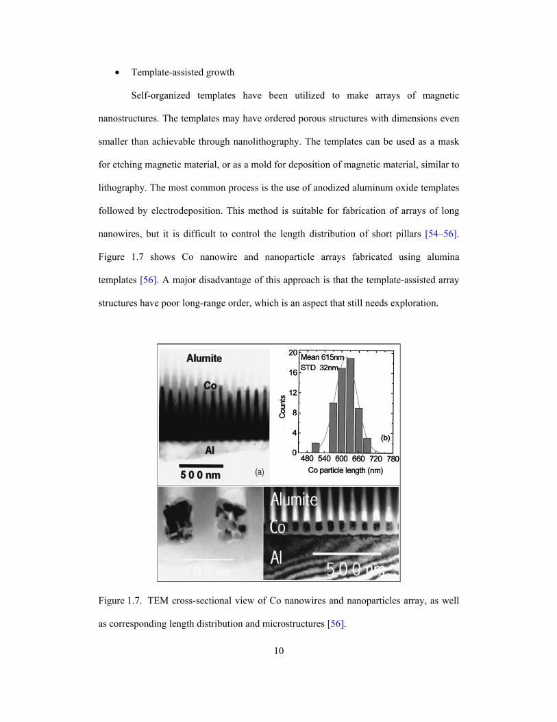
Figure 1.7 shows Co nanowire and nanoparticle arrays fabricated using alumina
templates [56]. A major disadvantage of this approach is that the template-assisted array
structures have poor long-range order, which is an aspect that still needs exploration.
Figure 1.7. TEM cross-sectional view of Co nanowires and nanoparticles array, as well
as corresponding length distribution and microstructures [56].
10

• Self assembly
Self assembly is a process whereby a system can organize itself to form a well-
ordered structure or pattern. Nanoparticles can be self-assembled onto a substrate to form
a regular array with very fine-scale structures over a large-scale area. This rapid, fine-
featured, large-scaled synthesis has great potential for applications if the following
drawbacks can be solved. The most critical problem is the need to control the particle size
distribution to obtain uniform magnetic properties. Moreover, oxidation and
agglomeration may affect the structure and separation of array elements, especially for
magnetic nanoparticles. Monodispersed magnetic nanoparticle (FePt, Co, etc.) arrays
with narrow size distribution and readily controlled composition [57–60], as shown in
Figure 1.8, have been synthesized through a solution phase route. It was also suggested
that self-assembly combined with templates could be used to improve the long-range
order.
Figure 1.8. TEM images showing monodispersed FePt nanoparticle arrays [57].
11

1.2.2. Characterization
For magnetic recording media, scanning electron microscopy (SEM) and atomic
force microscopy (AFM) can be used for characterization of morphology and surface
topography, while transmission electron microscopy (TEM) is suitable for microstructure
observation and analytical spectroscopy. In practice, due to the difficulty of detecting the
small signal from a single nanoparticle, magnetic properties are usually measured by
averaging over large arrays of identical nanoelements, using, for example, vibrating
sample magnetometry (VSM), superconducting quantum interference device (SQUID),
etc. [61]. In addition, several microscopic techniques can also be used to characterize
magnetic structures and switching behavior for either individual nanoelements or large-
scale arrays. Several of these commonly used techniques are described below.
The Magneto-Optic Kerr Effect (MOKE) involves measurement of the reflected
light from a magnetized surface which is changed in both polarization and reflectivity.
Since the change in polarization or reflectivity is directly proportional to the
magnetization close to the surface, MOKE has been used to measure magnetic hysteretic
response, especially in thin films [62–64]. Depending on the different geometries of the
magnetization vector with respect to the reflecting surface and the plane of incidence, the
technique can be categorized in three forms which are referred to as polar, longitudinal,
and transverse MOKE. Unlike other quantitative techniques, i.e. SQUID and VSM,
MOKE cannot yield an absolute value for magnetization; typical hysteresis loops are
averaged and normalized to unity at saturation. Moreover, MOKE cannot measure the
properties of an individual nanoscale element due to the detection limit. A typical MOKE
magnetometer is schematically shown in Figure 1.9 [62].
12

Figure 1.9 Schematic diagram of MOKE magnetometer apparatus [62].
Magnetic force microscopy (MFM) is a special type of AFM. The principle of
MFM is based on AFM, but the probe consists of magnetic material so that magnetic
interactions between probe and specimen can be detected [65, 66]. The MFM can thus
image the stray magnetic field above the surface of a sample, as depicted in Figure 1.10.
A magnetic tip is brought into close proximity with the surface and scanned over the
surface to reveal the magnetic domain structure of the sample at up to 50 nm resolution.
Since it is possible to apply external magnetic fields during measurement, the field
dependence of domain structures and magnetic reversal processes can be observed. The
advantages of MFM include that minimal sample preparation is required, and smaller
single elements can be examined. However, MFM imaging contains information about
both the topography and the magnetic properties of a surface, and the complicated
13

Figure 1.10. Schematic diagram showing principle of MFM.
interaction between the magnetic tip and the specimen surface makes quantitative
interpretation very difficult [67].
Scanning Electron Microscopy with Polarization Analysis (SEMPA) is a special
SEM technique developed for characterizing very small magnetic structures. SEMPA
images magnetization by measuring the spin polarization of secondary electrons emitted
in a SEM. Since secondary electron spin polarization is directly related to the
magnetization of the sample, SEMPA produces a direct image showing the magnitude
and direction of the magnetization in the region probed by the incident electron beam, as
sketched in Figure 1.11 [68]. SEMPA takes advantage of the SEM characteristics of high
spatial resolution (~10 nm), long working distance, and large depth of field, and also
allows magnetization measurements independent of the topographic structures. However,
the surface sensitivity (~1 nm depth) clearly limits its application for bulk materials.
14

Figure 1.11. Schematic diagram showing the principle of SEMPA [68].
Photoemission electron microscopy (PEEM) is an imaging technique that uses
the secondary electrons emitted from a sample surface upon absorption of photons in
ionizing radiation [69]. Modern PEEMs can routinely approach 10 nm resolution or
better, and are sensitive to specimen surface. Using circularly polarized x-rays to
stimulate photoelectrons, magnetic contrast can be added through the X-ray magnetic
circular dichroism (XMCD) effect. By combining the element sensitivity of time-
resolved XMCD with the spatial resolution of PEEM, XMCD-PEEM is a very powerful
technique for investigating magnetization dynamics in thin-film systems, especially
vortex propagation and DW motion in nanomagnets [70–72].
TEM-based magnetic imaging techniques, such as Lorentz microscopy and
electron holography, are the primary characterization methods in this dissertation
research. Details of these techniques are described in a later section (§2.4).
1.2.3. Magnetic properties
For the purpose of data recording applications, the ideal properties for patterned
media are well-defined remanent states, reproducible magnetization reversal process, and
15

narrow switching field distribution. In practice, there are two major factors that affect the
magnetic properties of nanomagnets – size and anisotropy.
It is well known that when the physical dimensions of a system become
comparable to characteristic length scales of a given physical property, these properties
can be severely affected. In the case of magnetism, the main characteristic length scales
are the exchange length (lex), and the magnetic DW thickness (δ), which are on the order
of ten to several tens of nanometers for most common magnetic materials. From the
energy point of view, the magnetic properties of nanomagnets depend sensitively on the
balance of exchange energy, magnetostatic energy, anisotropy energy, and Zeeman
energy [11, 61]. Exchange coupling aligns the spins parallel to each other so that the
existence of a uniform state of magnetization within the material minimizes the exchange
energy. On the other hand, the competing tendency to minimize magnetostatic energy
favors closed magnetization states, which can be achieved by the formation of DWs or
vortices. The magnetic microstructure and behavior of a magnetic material are highly
size-dependent: as the dimensions become on the order of lex, the magnetization
configuration of the material will go from a multidomain state to a closure domain state.
Moreover, when the size becomes smaller than lex, the magnetization evolves from
closure domain to single domain; and if the size becomes sufficiently small, the
magnetization will finally go from a single domain state to superparamagnetic [61].
Effects of size dependence on remanent configuration and switching behavior as
functions of sample diameter and thickness have been determined experimentally, as
illustrated in the phase diagram in Figure 1.12 [73]. This study showed a transition from
multidomain or vortex states to a single-domain state as the element size was decreased,
and similar tendencies were found as the thickness was decreased. Switching fields
typically increase as the particles become smaller, and their behavior approximates more
16

Figure 1.12. Experimentally determined phase diagram showing different magnetic
reversal mechanisms in terms of () vortex, or () single domain behavior [73].
closely to coherent rotation. However, particles with dimensions of 100 nm or above
generally show non-uniform reversal [11].
Anisotropy controls magnetic properties in terms of the tendency to align
magnetization along the easy axis of magnetic particles. Magnetic anisotropies include
magnetocrystalline anisotropy, which represents an intrinsic material property, and shape
anisotropy, which can be defined by controlling the shape of individual particles. For
patterned magnetic media, especially for polycrystalline systems that minimize the
intrinsic anisotropy by averaging over random orientations, shape anisotropy plays a
critical role in determining their magnetic behavior. Nanopatterned magnetic elements
with different shapes have been studied. The patterns include linear shapes, such as
triangles, squares, pentagons, hexagons [15, 32, 49], and circular shapes, such as disks
[17, 25], ellipses [30, 34, 35, 53], rings [19–24, 48], elliptical rings [26, 27], and slotted
elements [36–42, 47, 50, 52].
17

For polygonal elements, the magnetization can appear as vortices, or complex
twisted patterns, depending on the element size and geometry, initial saturation field, and
presence of any defects. Due to the asymmetry between demagnetization and element
geometry (shape anisotropy), the magnetization would tend to be parallel to the element
edges, and twist inside the element, as indicated in Figure 1.13 [49]. However, since
many parameters are involved but few can be easily interpreted, it is very difficult to
draw useful conclusions from existing results.
Circular shapes were designed with the intent to obtain simple flux-closure (FC)
states with opposite chiralities (Figure 1.14 (b)), which could technically be used as
binary storage bits [49]. However, high-energy vortex cores were often introduced during
magnetization reversal, and “S”-states were formed by shifting the FC center away from
the geometric disk center, as shown in Figure 1.14 (a). To eliminate the presence of such
vortex cores, ring-shaped elements were proposed, and so-called “onion” states were
observed at remanence, as shown in Figure 1.14 (c). Furthermore, slots were also
introduced as a geometric restriction to force the formation of stable flux closures, as
indicated in Figure 1.14 (d).
Figure 1.13. Electron holographic phase images of magnetic elements with shape of
triangle, square, pentagon, and hexagon, indicating twisted magnetization patterns at
remanent state [49].
18

Figure 1.14. Electron holographic phase images of magnetic elements with different
magnetization patterns at remanent state: (a) disk with “S”-state; (b) disk with FC state;
(c) ring with “Onion” state; (d) slotted-ring with FC state [49].
Elements with different shapes exhibit different magnetization reversal
mechanisms. For elements with solid shapes, vortices are generally involved in reversal
processes. For polygons with the same area, the field needed for sweeping out the vortex
increases as the shape becomes more like a disk [32]. Due to the sensitivity of shape
fluctuations and edge roughness, linear shapes usually have more complicated switching
processes than circular shapes. For ring-shaped elements, magnetization reverses between
flux-closures and onion states by means of the movement of head-to-head DWs [19], and
the switching fields are found to be strongly dependent of the ratio of inner and outer
diameters [48].
For magnetic particles with a specific geometry, shape anisotropy is directly
dependent on the lateral aspect ratio. Figure 1.15 shows MFM images of elliptical
elements with different aspect ratios at remanent state [74]. The single-domain
configuration was observed in elements with an aspect ratio larger than 5. A typical
vortex state was visible in thinner elements (23 nm) with aspect ratios of 2 and 3, but
thicker elements (42 nm) showed more diverse domain structure and complex
configurations, including two-vortex state, mixed state (vortex and cross-tie walls), and
19

cross-tie walls, with aspect ratios of 2, 3, and 4, respectively. It was also found that the
switching fields of small elements with aspect ratio less than 5 were significantly
dependent on the aspect ratio, due to shape anisotropy. However, the switching fields of
the ellipses with aspect ratios larger than 5 did not show obvious dependence on the
aspect ratio. In other words, the switching fields of uniform magnetization reversal were
almost independent of the aspect ratio.
Figure 1.15. MFM images of elliptical Permalloy elements with aspect ratios varying
from 2 to 10 at the remanent state: (a) 23 nm in thickness after saturation to the right, and
(b) 42 nm in thickness after saturation to the left. The schematic diagrams on the left
indicate the magnetization configurations for clarity [74].
20

When individual elements are patterned in arrays, the interactions between these
elements introduce new anisotropies into the system. This anisotropy can be treated, to a
first-order approximation, as the effect of dipole interaction (or fringing field) within the
entire arrays. Depending on the different arrangements of individual dipolar fields
relative to the characteristic anisotropy of the array, the overall switching mechanism can
be represented in terms of two different hysteresis loops, as shown in Figure 1.16 [61].
Moreover, due to the high demands of storage density, magnetic elements are being
patterned more and more densely in arrays. Therefore, another non-negligible interaction
is the effect of magnetostatic fields. A direct drawback of these effects is to cause a
spread of switching field distribution: the shearing of hysteresis loops and the occurrence
of steps can be considered as experimental evidence of such interactions.
Figure 1.16. Schematic showing the effect of dipole interaction between two magnetic
particles [61].
21

1.2.4. Advances and challenges
Patterned magnetic nanostructures are being researched and developed because
of the demand for ultrahigh-density storage technology. As the extension of conventional
longitudinal recording, patterned media are well on the way to reach 1 Tbit/in2 by
continuous scaling-down of bit size and improving noise performance. Moore’s Law is
the current guideline for the evolution of this technology [10]. However, these
developments will eventually approach the physical limits of atomic structures due to
thermal instability, or the so-called superparamagnetic limit, where the anisotropy energy
KuV is not sufficiently large enough relative to the environmental thermal energy kBT, and
the magnetization becomes randomized losing any stored information. Alternative
approaches to circumvent these physical limits are expected to emerge by either utilizing
novel materials or via new emerging technologies. Practical engineering issues can
intervene to block progress towards the physical limits. For example, inevitable defects
during fabrication can cause non-negligible irregularities in device performance, which
will result in a tradeoff between the area of patterning and the shape accuracy. Another
concern relates the characterization methods and instrumentation. More and more
sensitivity is required due to the ongoing miniaturization of recording bit elements.
Although micromagnetic simulations can be of great value for designing structures and
understanding their magnetic behavior, new analytical methods need to be developed in
order to realize better resolution and accuracy, direct visualization, and quantitative data
acquisition, as well as demonstrating technical feasibility for industrial applications.
22

1.3. Magnetic Domain Wall and Related Devices
1.3.1. Racetrack memory
In a magnetic nanowire (NW), the magnetization of each domain should be
confined along the long axis of the wire, aligning along one of two possible directions.
Domains having two opposite magnetization configurations could be used to represent
binary information, and thus precise control of the DW in between the adjacent recording
domains (or bits) would enable read/write processes in a NW-based device. Based on this
principle, Parkin and co-workers proposed and developed the so-called “racetrack
memory” as an emerging technology for non-volatile magnetic random access memory
(MRAM) devices [75–77]. In the racetrack memory, the series motion of DWs along a
magnetic NW shift register would be controlled using spin-polarized current pulses. The
physical effect in current-driven DW motion is based on a spin-momentum transfer
torque (or spin torque) that is exerted by spin-polarized conduction electrons on the
magnetic moments in the wire, so that the DW would move as the torque rotates the
moments. In contrast to current magnetic hard drives where a disk mechanically spins
under a head that reads the data stored on the disk at fixed positions, the current pulses
would trigger the DW movements electronically to a locally fixed read-out sensor, as
illustrated in Figure 1.17 [75]. This novel concept would combine the advantages of both
solid-state and magnetic memory devices, and make ultrahigh recording density possible
by squeezing the NWs in a three-dimensional (3D) arrangement. However, there are
several open questions blocking the transition from theoretical principles to practical
technology, which still need better understanding of the physics and materials involved.
23

Figure 1.17. Schematic showing principle of racetrack memory using pulse-triggered
DW motion along magnetic NWs [75].
24

1.3.2. Domain-wall logic
Although NW/DW-based devices are being used as memory elements in hard
disk and MRAM devices, they are limited to the extent that information can only be
stored, but not manipulated in magnetic form. Cowburn and his group expanded the
scope and proposed DW logic gates, which would make computation between the
magnetic data bits possible [78]. A basic logic gate would be built using one or more
ferromagnetic NWs patterned in special designs to realize specific Boolean logic
functionality, including AND, NOT, fan-out, and cross-over, as summarized in Figure
1.18 [79]. The underlying principle of these logic gates is to use the swap of DWs as a
switch between input and output signals. These basic logic building blocks could be
linked together into complex NW networks, and controlled in-plane by an applied
oscillating magnetic fields.
In contrast to conventional semiconductor-based logic circuits, these DW logic
devices would use no diodes or transistors, and thus offer great potential for an increase
in integration density and reduction in power dissipation over current microelectronic
technology. The planar layout of the entire NW network would in principle enable
numerous layers of such networks to be stacked on top of each other to realize 3D
architectures, resulting in dramatic improvement of device minimization. In addition,
because the DW logic operations would be carried out by magnetic-field-driven DW
motion, current would not involved, nor would much heating be generated that would
cause data switching.
The prospects for these developments appear bright, though there are many
questions and issues being discussed. Much in-depth investigation will be needed as the
devices are scaled down and integrated with electronic circuits.
25

Figure 1.18. Summary of conventional CMOS circuit elements and corresponding
DW logic elements to realize different logic functionalities [79].
26

1.3.3. Research progress and challenges
A comprehensive understanding of magnetic DW properties is essential for
successful development of these memory and logic devices. Relevant research topics
include DW propagation and motion (nucleation, injection, pinning, depinning, etc.),
driven forces (spin-polarized currents, or magnetic fields), DW types and configurations
(transverse/vortex, head-to-head/tail-to-tail), DW velocity, correlation of current (density,
pulse length) and DW pinning fields, DW dynamics, and many other aspects [75–88].
Figure 1.19 shows examples of DW motion in Permalloy (Py, Ni81Fe19) NW or
NW networks within racetrack memory and DW logic devices [76, 79]. As indicated in
this figure, and oftentimes in the literature, the DW motion is probed by indirect
measurements of magnetization hysteresis loops and magnetoresistance (MR) changes of
the entire NW or regions distant from the DW interaction site. However, these techniques
Figure 1.19. Examples of typical studies on racetrack memory and DW logic [76, 79].
27

28
.
1.4. utline of Dissertation
issertation has concentrated on quantitative magnetic
characte
rimental details of this dissertation research,
includin
versal of Co
nanorin
/Cu/Py
spin-va
pter 5 illustrates DW motion in Py NWs driven by in situ magnetic field. DW
propaga
lack the ability to provide direct visualization of DW behavior, e.g., type and position
Moreover, quantification and direct observation cannot simultaneously be achieved using
these conventional techniques, for studies of both current- and magnetic-field-driven DW
propagation. Thus, quantitative nanoscale magnetic imaging is critical to provide basic
information about nanomagnetism and spintronic materials.
O
The research of this d
rization of patterned magnetic nanostructures and devices using advanced
electron microscopy techniques, namely off-axis electron holography, and Lorentz
microscopy. The investigation can be roughly separated into three major parts, according
to different materials of interest: (i) monolayer Co nanorings; (ii) multilayer spin-valve
nanorings; (iii) Py notched nanowires.
Chapter 2 summarizes expe
g nanofabrication, characterization, and micromagnetic simulations.
Chapter 3 shows the results of remanent states and magnetization re
gs with and without slots, where vortex-controlled switching behavior is
identified and comparison between observation and simulation is also carried out.
Chapter 4 describes different remanent and switching behaviors of Co
lve nanorings, as a function of the different applied field directions relative to the
slot directions. In addition, interlayer coupling and multi-step hysteresis loops are also
quantified.
Cha
tions, including nucleation, injection, pinning and depinning, are directly
observed, and critical switching fields are statistically analyzed. A unique asymmetrical

29
s the important conclusions and advances achieved in this
work, a
DW pinning behavior is also recognized, depending on DW chirality relative to the sense
of rotation around the notch.
Chapter 6 summarize
s well as providing prospective scope for future studies.

30
Referen s
. Oersted, Annals of Philosophy. 16, 273 (1820).
aterials, Chapman & Hall, London (1998).
, Modern Magnetic Materials, Wiley, New York (2000).
s, New York (2001).
R. Schäfer, Magnetic Domains: the Analysis of Magnetic Microstructures, Springer-Verlag, Berlin (1998).
etunion. 8, 153 (1935).
988).
agn. 24, 2476 (1994).
.
H. W. Kesteren, J. Appl. Phys. 87, 5398 (2000).
agn. Mater. 272–276, 1692 (2004).
2000).
, 3457 (2003).
. A. C. Bland, Z. Cui, and R. Speaks, Phys. Rev. Lett. 86, 1098 (2001).
, and Y. Chen, J. Appl. Phys. 92, 7397 (2002).
, J. Rothman, J. A. C. Bland, W. Wernsdorfer, G. Faini, and E. Cambril, Phys. Rev. Lett. 90, 097202 (2003).
ce
[1] H. C
[2] D. Jiles, Introduction to Magnetism and Magnetic M
[3] R. C. O’Handley
[4] S. Blundell, Magnetism in Condensed Matter, Oxford University Pres
[5] A. Hubert,
[6] L. D. Landau and E. M. Lifschitz, Physik Z. Sowj
[7] O. Smith, The Electrical World. 12, 116 (1888).
[8] F. Engel, J. Audio Eng. Soc. 36, 170 (1986).
[9] H. H. K. Thiele, J. Audio Eng. Soc. 36, 396 (1
[10] E. Grochowshi and D. A. Thompson, IEEE Trans. M
[11] C. A. Ross, Annu. Rev. Mater. Res. 31, 203 (2001).
[12] A. S. Hoagland, IEEE Trans. Magn. 39, 1871 (2003)
[13] J. J. M. Ruigrok, R. Coehoorn, S. R. Cumpson, and
[14] J. C. Lodder, J. Magn. M
[15] R. P. Cowburn, J. Phys. D: Appl. Phys. 33, R1 (2000).
[16] R. P. Cowburn and M. E. Welland, Science. 287, 1466 (
[17] R. P. Cowburn, J. Appl. Phys. 93, 9310 (2003).
[18] D. K. Koltsov and M. E. Welland, J. Appl. Phys. 94
[19] J. Rothman, M. Kläui, L. Lopez-Diaz, C. A. F. Vaz, A. Bleloch, J
[20] S. P. Li, W. S. Lew, J. A. C. Bland, M. Natali, A. Lebib
[21] M. Kläui, C. A. F. Vaz

31
eyderman, F. Nolting, A. Pavlovska, E. Bauer, S. Cherifi, S. Heun, and A. Locatelli, Appl. Phys. Lett. 85,
, D. Backes, W. Bührer, D. Bedau, M. Kläui, U. Rüdiger, C. A. F. Vaz, J. A. C. Bland, L. J. Heyderman, F. Nolting, S. Cherifi, A. Locatelli, R.
Gardiner, W. Y. Lee, and J. A. C. Bland, J. Appl. Phys. 87, 7019 (2000).
h. Gasser, and L. Lopez-Diaz, J. Appl. Phys. 99, 063904 (2006).
pl. Phys. 36, 2031 (2003).
J. Appl. Phys. 97, 053902 (2005).
oft, C. A. Ross, R. Menon, and H. I. Smith, J. Appl. Phys. 97, 10K113 (2005).
. Dunin-Borkowski, S. B. Newcomb, M. R. McCartney, F. J. Castaño, and C. A. Ross, J. Appl. Phys. 98, 013903 (2005).
237 (1999).
omez, T. V. Luu, A. O. Pak, K. J. Kirk, and J. N. Chapman, J. Appl. Phys. 85, 6163 (1999).
J. N. Chapman, and C. D. W. Wilkinson, J. Appl. Phys. 89, 7174 (2001).
Scheinfein, J. N. Chapman, S. McVitie, M. F. Gillies, B. R. Ward, and J. G. Tennant, J. Phys. D: Appl. Phys. 34, 160 (2001).
ppl. Phys. Lett. 84, 4406 (2004).
pman, S. McVitie, and C. D. W. Wilkinson, J. Appl. Phys. 96, 5173 (2004).
. K. Hong, S. H. Gee, D. W. Erickson, and B. C. Choi, Appl. Phys. Lett. 83, 329 (2003).
ng, S. H. Gee, D. W. Erickson, T. Tanaka, and B. C. Choi, J. Appl. Phys. 95, 7019 (2004).
Chipeniuk, B. C. Choi, M. H. Park, Y. K. Hong,
[22] M. Kläui, C. A. F. Vaz, J. A. C. Bland, L. J. H
5637 (2004).
[23] M. Laufenberg
Belkhou, S. Heun, and E. Bauer, Appl. Phys. Lett. 88, 052507 (2006).
[24] Y. B. Xu, A. Hirohata, L. Lopez-Diaz, H. T. Leung, M. Tselepi, S. M.
[25] L. J. Heyderman, S. Czekaj, F. Nolting, E. Müller, P. Fischer, P
[26] F. J. Castaño, C. A. Ross, and A. Eilez, J. Phys. D: Ap
[27] C. A. Ross, F. J. Castaño, E. Rodriguez, S. Haratani, B. Vögeli, and H. I. Smith,
[28] W. Jung, F. J. Castaño, D. Morecr
[29] T. Kasama, P. Barpanda, R. E
[30] K. J. Kirk, J. N. Chapman, and C. D. W. Wilkinson, J. Appl. Phys. 85, 5
[31] R. D. G
[32] K. J. Kirk, S. McVitie,
[33] K. J. Kirk, M. R.
[34] X. Liu, J. N. Chapman, S. McVitie, and C. D. W. Wilkinson, A
[35] X. Liu, J. N. Cha
[36] M. H. Park, Y
[37] M. H. Park, Y. K. Ho
[38] B. R. Pujada, J. Svendsen, K. O.

S. H. Gee, and D. W. Erickson, J. Appl. Phys. 96, 4362 (2004).
32
[39] B. C. Choi, J. Ho, Y. K. Hong, M. H. Park, H. Han, S. H. Gee, and G. W.
[40] B. R. Pujada, B. C. Choi, M. H. Park, Y. K. Hong, S. H. Gee, H. Han, and G. W.
[41] B. C. Choi, B. R. Pujada, Y. K. Hong, M. H. Park, H. Han, S. H. Gee, and G. W.
[42] H. Han, Y. K. Hong, M. H. Park, B. C. Choi, S. H. Gee, J. F. Jabal, G. Abo, A.
[43] R. E. Dunin-Borkowski, M. R. McCartney, B. Kardynal, and D. J. Smith, J.
[44] D. J. Smith, R. E. Dunin-Borkowski, M. R. McCartney, B. Kardynal, and M. R.
[45] R. E. Dunin-Borkowski, M. R. McCartney, B. Kardynal, M. R. Scheinfein, and
[46] R. E. Dunin-Borkowski, M. R. McCartney, B. Kardynal, M. R. Scheinfein, D. J.
[47] H. Hu, H. Wang, M. R. McCartney, and D. J. Smith, J. Magn. Magn. Mater. 290-
[48] H. Hu, H. Wang, M. R. McCartney, and D. J. Smith, J. Appl. Phys. 97, 054305
[49] H. Wang, H. Hu, M. R. McCartney, and D. J. Smith, J. Magn. Magn. Mater. 303,
[50] H. Hu, H. Wang, M. R. McCartney, and D. J. Smith, Phys. Rev. B 73, 153401
[51] N. Agarwal, H. Wang, D. J. Smith, and M. R. McCartney, IEEE Trans. Magn.
[52] N. Agarwal, M. R. McCartney, and D. J. Smith, J. Appl. Phys. 102, 023911
[53] K. S. Buchanan, P. E. Roy, M. Grimsditch, F. Y. Frandin, K. Yu. Guslienko, S.
[54] J. M. García, A. Asenjo, J. Velázquez, D. García, M. Vázquez, P. Aranda, and E.
[55] R. M. Metzger, V. V. Konovalov, M. Sun, T. Xu, G. Zangari, B. Xu, M. Benakli,
Donohoe, IEEE Trans. Magn. 41, 2709 (2005).
Donohoe, J. Appl. Phys. 97, 073904 (2005).
Donohoe, IEEE Trans. Magn. 41, 3109 (2005).
Lyle, B. Wong, and G. W. Donohoe, IEEE Trans. Magn. 41, 4341 (2005).
Appl. Phys. 84, 374 (1998).
Scheinfein, J. Appl. Phys. 87, 7400 (2000).
D. J. Smith, J. Microsc. 200, 187 (2000).
Smith, and S. S. P. Parkin, J. Appl. Phys. 90, 2899 (2001).
291, 234 (2005).
(2005).
237 (2006).
(2006).
42, 2414 (2006).
(2007).
D. Bader, and V. Novosad, Nature Phys. 1, 172, (2005).
Ruiz-Hitzky, J. Appl. Phys. 85, 5480 (1999).

and W. D. Doyle, IEEE Trans. Magn. 36, 30 (2000).
33
[56] M. Sun, G. Zangari, M. Shamsuzzoha, and R. M. Metzger, Appl. Phys. Lett. 78,
[57] S. H. Sun, C. B. Murray, D. Weller, L. Folks, and A. Moser, Science. 287, 1989
[58] S. H. Sun, E. E. Fullerton, D. Weller, and C. B. Murray, IEEE Trans. Magn. 37,
[59] A. Moser, K. Takano, D. T. Margulies, M. Albrecht, Y. Sonobe, Y. Ikeda, S. H.
[60] B. D. Terris and T. Thomson, J. Phys. D: Appl. Phys. 38, R199 (2005).
[61] J. I. Martín, J. Nogués, K. Liu, J. L. Vicente, and I. K. Schuller, J. Magn. Magn.
[62] D. A. Allwood, G. Xiong, M. D. Cooke, and R. P. Cowburn, J. Phys. D: Appl.
[63] Z. Q. Qiu and S. D. Bader, Rev. Sci. Instrum. 71, 1243 (2000).
[64] M. Grimsditch and P. Vavassori, J. Phys.: Condens. Matter 16, R275 (2004).
[65] Y. Martin and H. K. Wickramasinghe, Appl. Phys. Lett. 50, 1455 (1987).
[66] D. Rugar, H. J. Mamin, P. Guethner, S. E. Lambert, J. E. Stern, I. McFayden, and
[67] A. Wadas and P. Grütter, Phys. Rev. B 39, 12013 (1989).
[68] M. R. Scheinfein, J. Unguris, M. H. Kelley, D. T. Pierce, and R. J. Celotta, Rev.
[69] S. Anders, H. A. Padmore, R. M. Duarte, T. Renner, T. Stammler, A. Schöll, M.
[70] T. Taniuchi, M. Oshima, H. Akinaga, and K. Ono, J. Appl. Phys. 97, 10J904
[71] X. F. Han, M. Grimsditch, J. Meersschaut, A. Hoffmann, Y. Ji, J. Sort, J.
[72] V. Uhlíř, S. Pizzini, N. Rougemaille, J. Novotný, V. Cros, E. Jiménez, G. Faini,
2964 (2001).
(2000).
1239 (2001).
Sun, and E. E. Fullerton, J. Phys. D: Appl. Phys. 35, R157 (2002).
Mater. 256, 449 (2003).
Phys. 36, 2175 (2003).
T. Yogi, J. Appl. Phys. 68, 1169 (1990).
Sci. Instrum. 61, 2501 (1990).
R. Scheinfein, J. Stohr, L. Séve, and B. Sinkovic, Rev. Sci. Instrum. 70, 3973 (1999).
(2005).
Nogue´s, R. Divan, J. E. Pearson, and D. J. Keavney, Phys. Rev. Lett. 98, 147202 (2007).
L. Heyne, F. Sirotti, C. Tieg, A. Bendounan, F. Maccherozzi, R. Belkhou, J. Grollier, A. Anane, and J. Vogel, Phys. Rev. B 81, 224418 (2010).

34
, and D. M. Tricker, Phys. Rev. Lett. 83, 1042 (1999).
. C. Wu, Z. H. Wei, M. F. Lai, and C. R. Chang, IEEE Trans. Magn. 41, 947 (2005).
ience 320, 190 (2008).
ience 320, 209 (2008).
L. Thomas, R. Moriya, C. Rettner, X. Jiang, and S. S. P. Parkin, Phys. Rev. Lett. 97, 207205 (2006).
aulkner, D. Atkinson, D. Petit, and R. P. Cowburn, Science 306, 1688 (2005).
Cooke, C. C. Faulkner, D. Atkinson, N. Vernier, and R. P. Cowburn, Science, 296, 2003 (2002).
ppl. Phys. 103, 114307 (2008).
ng, D. Read, D. Petit, A.V. Jausovec, L. O’Brien, E.R. Lewis, and R. P. Cowburn, Appl. Phys. Lett. 94, 103113 (2009).
n, Appl. Phys. Lett. 91, 022506 (2007).
hea, S. McVitie, J. N. Chapman, and J. M. R. Weaver, Appl. Phys. Lett. 93, 202505 (2008).
haverbeke, D. Atkinson, R. Allenspach, and C. H. Marrows, Phys. Rev. Lett. 102, 127203 (2009).
ierce, and J. Unguris, J. Appl. Phys. 105, 103902 (2009).
cklage, P. Fischer, and G. Meier, Phys. Rev. Lett. 102, 147204 (2009).
guchi, T. Ono, S. Nasu, K. Miyake, K. Mibu, and T. Shinjo, Phys. Rev. Lett. 92, 077205 (2004).
, L. Heyne, P. Möhrke, D. Backes, J. Rhensius, U. Rüdiger, L. J. Heyderman, T. O.Mentes, M. A. Nino, A. Locatelli, A. Potenza, H.
[73] R. P. Cowburn, D. K. Koltsov, A. O. Adeyeye, M. E. Welland
[74] C. C. Chang, Y. C. Chang, W. S. Chung, J
[75] S. S. P. Parkin, M. Hayashi, and L. Thomas, Sc
[76] M. Hayashi, L. Thomas, R. Moriya, C. Rettner, and S. S. P. Parkin, Sc
[77] M. Hayashi,
[78] D. A. Allwood, G. Xiong, C. C. F
[79] D. A. Allwood, Gang Xiong, M. D.
[80] D. Petit, A.V. Jausovec, D. Read, and R. P. Cowburn, J. A
[81] H. T. Ze
[82] D. McGrouther, S. McVitie, and J. N. Chapma
[83] K. J. O’S
[84] S. Lepadatu, A. Van
[85] W. C. Uhlig, M. J. Donahue, D. T. P
[86] M. Y. Im, L. Bo
[87] A. Yama
[88] T. A. Moore, M. Kläui
Marchetto, S. Cavill, and S. S. Dhesi, J. Magn. Magn. Mater. 322, 1347 (2010).

35
CHAPTER 2
EXPERIMENTAL DETAILS
This chapter provides detailed information about the facilities and instruments, as
well as the procedures of sample preparation and characterization, that were involved in
this dissertation research. The chapter also describes the principle of micromagnetic
modeling and the essential materials parameters used for typical simulations. Details
about electron hologram acquisition, phase reconstruction, quantification, and magnetic
representation are introduced, followed by several practical examples of quantitative
phase imaging of magnetic fields in different materials.
2.1. Instrumentation
2.1.1. Electron beam lithography
A typical EBL system consists of the following parts: (i) electron source that
supplies electrons; (ii) column of electron lenses and deflection coils that control and
focus the electron beam; (iii) mechanical stage that positions the sample under the
electron beam; and (iv) computer system that controls the instrument [1].
The JEOL JBX-6000FS/E EBL system located in the Center for Solid State
Electronics Research (CSSER) has been used in this research. This instrument is a vector-
scanning-type EBL system which has two operation modes: the 4th-lens mode and the
5th-lens mode. The former mode is used for submicron lithography while the latter mode
is used for ultra-fine lithography. The lens system consists of two intermediate lenses
(2nd and 3rd lenses) and one objective lens (4th or 5th lens), as shown in Figure 2.1. A
high-brightness electron gun using zirconium-oxide-coated tungsten thermal-field-emitter
(ZrO/W TFE) and an in-lens deflector has been employed. The acceleration voltage is

36
usually set at 50 kV. In the 5th-lens mode, the electron beam has a minimum spot
diameter of 5 nm. Workpiece stage movement is driven by the step-and-repeat method,
with the stage position increment of 0.62 nm controlled by a laser interferometer.
Figure 2.1. Electron optics system of JBX-6000FS/E [1].

37
umn, a
eam of electrons is emitted by an electron gun, accelerated by high voltage (usually
100–400 kV), focused by electrostatic or electromagnetic lenses, and then transmitted
through an ultrathin specimen, interacting with the specimen as it passes through. An
image is formed by an objective lens from the electrons transmitted through the
specimen, which is then magnified onto the final imaging screen or detector. Images can
be viewed on a fluorescent screen, and recorded by photographic film, or a charge-
coupled device (CCD) camera. A typical TEM is schematically shown in Figure 2.2.
2.1.2. Transmission electron microscopy
Transmission electron microscopy (TEM) is an imaging technique that allows
high-resolution observation of materials at the atomic scale. Inside the TEM col
b
heme. Figure 2.2. Schematic for a TEM and its electron optics sc

38
in the John M. Cowley Center for High
Resolut
eld-
free conditions. In addition, an X-ray detector and an energy-selecting Gatan imaging
filter (GIF) are also attached to provide analytical characterization, such as energy-
dispersive X-ray spectroscopy (EDS) and electron-energy-loss spectroscopy (EELS).
2.2. Fabrication
Ferromagnetic nano-elements with different shapes can be fabricated by direct
patterning onto 50-nm-thick self-supporting electron-transparent 500×500µm silicon-
nitride TEM membrane windows using the EBL technique and a standard lift-off process
[2]. The processing was carried out in the CSSER class-100 cleanroom. Figure 2.3
illustrates the geometry of the membrane samples used as substrates, with (a) top view,
(b) side view, and (c) actual image, respectively.
Before EBL processing, the desired shapes and distribution of the nanopatterned
arrays were written into data files using a combination of auto-computer-aided design
uto-CAD) software and JEOL machine code. The pattern data files were then
debugged free of any
The Philips-FEI CM200-FEG TEM
ion Electron Microscopy (CHREM) has been used in this research. This TEM is
normally operated at 200 kV, and it is equipped with a Schottky field-emission gun
(FEG) to provide highly coherent electron illumination, an electrostatic biprism located in
the selected-area aperture plane to enable the function of electron holography, and a
1024×1024 pixel Gatan 794 slow-scan CCD camera (later updated to a Gatan Orius
SC600 with 2680×2688 pixels) for digital recording. A special minilens (so-called
Lorentz lens, with CS = 8 m and 1.2 nm line resolution at 200 kV) located in the bore of
the objective lens pole-piece, allows images to be obtained at magnifications of up to
50kx with the main objective lens switched off and the sample located in almost fi
(A
converted to the internal format of the EBL machine codes and

Figure 2.3. Schematics showing the geometry and dimensions of the membrane samples:
(a) top view; (b) side view. (c) Actual image.
errors before exposure to the electron beam took place. One or two corner points of the
sample were usually used as reference marks to obtain the offset required for locating the
patterns on the membrane window. A few scratches were drawn on the frame to help in
fine-focusing of the sample surface during alignment of the EBL system.
Figure 2.4 illustrates the major processing steps during EBL fabrication. The
silicon nitride membranes were pre-cleaned in warm acetone for 15 minutes and then
rinsed in isopropyl alcohol (IPA) for 5 minutes, followed by nitrogen blow-drying. The
cleaning process ensured that the Si3N4 membranes were free from any contamination. A
2% polymethyl-methacrylate (PMMA) (in chlorobenzene) solution was spun at 5000 rpm
for 30 seconds onto the Si3N4 membranes, and then baked at 170°C in an oven for 1–2
hours. The baking time had to be long enough to ensure that the polymer resist was fully
baked and did not disintegrate catastrophically when exposed to the high-energy electron
beam. According to the pre-calibration curve of resist thickness as function of spin speed,
about 100-nm thickness of PMMA layer was obtained on the membranes after baking.
This PMMA thickness is a tradeoff between the preference for a thin resist layer required
39

40
Figure 2.4. Schematic outline of EBL process: (a) cleaning membrane; (b) spinning and
baking PMMA; (c) EBL exposure; (d) resist development; (e) deposition of magnetic
material; (f) lift off.

41
by the high-resolution EBL pattern writing, and the requirement that the thickness of the
resist layer should be at least 3 times thicker than the metal layer to be deposited in order
to facilitate the lift-off process. This cap on the maximum resist thickness limits the scope
for depositing multilayer structures with total stack heights exceeding 30 nm.
A very high area dose, 800 μC/cm2, was normally used to expose the patterns.
This very high dose was essential because of the reduced backscattering and secondary
electron yield from the very thin Si3N4 support membranes relative to a standard Si wafer.
The exposed membranes were developed in a solution of 11 : 10 : 1 methyl isobutyl
ketone : cellusol : methyl alcohol for 15 seconds, stopped by soaking in IPA for 20
seconds, and followed by blow-drying in nitrogen. The PMMA on the exposed areas was
removed completely after these steps. Particular caution was needed for handling the
nitride membrane windows during processing due to the extreme low strength and high
sensitivity to pressure or stress.
Ferromagnetic thin films were then deposited on the Si3N4 membranes using an
electron-beam evaporator (TorrVac VC-320) at a typical vacuum pressure of 3×10⁻⁶ Torr,
usually followed by deposition of a 2-nm-thick Al layer to avoid surface oxidation. The
deposition rate was kept as low as ~0.5 Ǻ per second. This slow deposition rate normally
ensured uniform deposition. As-deposited samples were lifted off using Microstrip 2001
(a commercial solvent) at 70°C for 4–5 hours to remove unwanted PMMA and the
verlaying materials, and the expected elements were left on the membrane windows.
p to prevent electrostatic charging during TEM observation.
o
After completion of the lift-off process, another layer of 2–3 nm Ti was deposited onto
the nitride membrane, using a separate thin-film deposition system under very high
vacuum, as a final ste
42
by several
compet
al EEEE +++= (2.1)
2.3. Micromagnetic Simulations
Micromagnetism is a classical theory for the treatment of magnetization
processes in ferromagnetic materials, and deals with the interactions between magnetic
moments on sub-micrometer length scales. These interactions are governed
ing energy terms: (i) magnetostatic energy (ES) or demagnetization energy (Edemag),
which originates from the classical long-range interactions between magnetic dipoles
within the object; (ii) exchange energy (Eex), which aligns the magnetic moments in the
short range parallel or anti-parallel to each other; (iii) magnetocrystalline anisotropy
energy (EK), which correlates magnetization and crystal lattice, and orients the
magnetization preferentially along certain crystallographic directions; and (iv) Zeeman
energy (EH), which rotates magnetic moments parallel to an external magnetic field. Thus,
the total magnetic Gibbs free energy of the system can be expressed as:
totE HKexS
Numerical micromagnetic simulations, based on either finite difference or finite
element methods, can resolve local arrangements of the magnetization in static situations,
as well as its dynamic evolution as a function of time. The space and time resolution is on
the order of nanometers and nanoseconds, respectively. For static problems where
thermal fluctuations and dynamic effects are usually neglected, micromagnetic
simulations start from the minimization of the total Gibbs free energy to determine the
stable equilibrium states for static problems. In order to study the time-dependent
dynamic response to an applied field, the Gilbert equation of motion has to be taken into
account [4]:
tMγ
t S ∂∂∂ MMΜ ×+×−=
∂HM αeff|| (2.2)
where γ s the gyromagnetic ratio |γ| = 2.210175×10⁵ m/As, α is dimensionless Gilbert i

43
This equation modifies the Landau-
Lifshitz
damping constant, Heff is effective magnetic field.
ordinary differential equation [5] by replacing the damping term, and is
mathematically equivalent to the Landau-Lifshitz-Gilbert (LLG) equation:
eff2eff2 1||
1|| HMMHMΜ ××
+−×
+−=
∂∂
SMγ
t ααγ
α (2.3)
In the present research, we used the object-oriented micromagnetic framework
(OOMMF) software package that was developed by Donahue and Porter from National
Institute of Standards and Technology (NIST) [6]. OOMMF is an open-source simulation
tool based on algorithm of finite difference lattice discretizations of space and FFT. The
codes are written in C++ with a Tcl/Tk algorithm interface, which provides much
portability and flexibility to users.
In practical simulations, geometrical and structural parameters of the magnetic
materials are obtained from TEM and electron holography
and technical parameters are listed in Table 2.1.
Table 2.1. Essential parameters used for practical micromagnetic simulations.
measurements. Other intrinsic
Parameters Co Py
Saturation magnetization (MS: A/m) 1.4×10⁶ 8.6×10⁵
Exchange stiffness (A: J/m) 3.0×10⁻¹¹ 1.3×10⁻¹¹
Uniaxial anisotropy constant (K1: J/m3) 6×10³ —
Damping constant 0.5 0.5
Cell size (nm3) 5×5×5 5×5×5

44
etic materials
because the specimen is immersed in the magnetic field of the objective lens, which i
usually sufficiently strong (~1.5–2 T) to saturate the material and thus destroy any
domain
passing through a region of magnetic induction in the
specime
2.4. Characterization
2.4.1. Lorentz microscopy
Standard TEMs are not well equipped for the study of magn
s
structure of interest. In contrast, Lorentz TEM can provide a field-free
environment for imaging of magnetic materials when the normal objective lens is
completely switched off. Lorentz microscopy has been used for several decades to study
magnetic domain structures and magnetization reversal mechanisms in magnetic thin
films and nanomagnets [7].
The interaction of electrons
n can result in magnetic image contrast, because of the deflection, as indicated in
Figure 2.5 (a), experienced by electrons, as determined by the Lorentz force:
)( BveFL ×−= (2.4)
where FL is the Lorentz force acting on an electron with elementary charge e traveling
with velocity v, and B is the magnetic induction averaged along the electron trajectory.
The direction of the vector product obeys the right-hand rule.
There are several modes of Lorentz microscopy including Fresnel mode,
Fou ntrast (DP [8, 9]. In our experiments,
the Fres ally used, with the Lorentz minile u ed so
tha was form er these conditio
domain walls e bright (convergent) and dark (divergent) lines, as
Figure 2.5 (b). This imaging mode is more powerful when a magnetic field is
in situ so that magnetization reversal processes can be observed rather than just
cault mode, and differential phase co C) mode
nel imaging mode was norm ns defoc s
t an out-of-focus image of the specimen ed. Und ns, magnetic
were imaged as alternat
shown in
applied

45
structure. Application of a magnetic field can be realized by
in the small vertical field caused by the partially excited
objectiv
imaging a static domain
tilting the specimen holder
e lens. Although Lorentz TEM oftentimes offers straightforward image
interpretation about magnetic information on domain and DW structures, there are still
significant drawbacks of using the Fresnel mode. Quantitative information is difficult to
obtain, and the direction of magnetization within any single domain cannot be easily
inferred. In addition, for multilayered materials, there is no simple way of separating
contributions to the images arising from the individual layers.
Figure 2.5. Schematic of (a) Lorentz force, and (b) Fresnel Lorentz imaging. Electrons
passing through the magnetic sample are deflected due to the in-plane magnetic field, and
form DW magnetic contrast at under- or over-focus conditions [9].
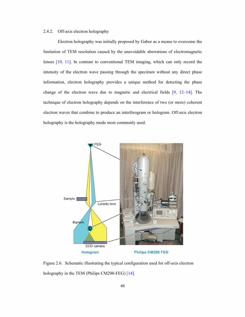
46
of two (or more) coherent
lectron waves that combine to produce an interferogram or hologram. Off-axis electron
holography is the holography mode most commonly used.
2.4.2. Off-axis electron holography
Electron holography was initially proposed by Gabor as a means to overcome the
limitation of TEM resolution caused by the unavoidable aberrations of electromagnetic
lenses [10, 11]. In contrast to conventional TEM imaging, which can only record the
intensity of the electron wave passing through the specimen without any direct phase
information, electron holography provides a unique method for detecting the phase
change of the electron wave due to magnetic and electrical fields [9, 12–14]. The
technique of electron holography depends on the interference
e
Figure 2.6. Schematic illustrating the typical configuration used for off-axis electron
holography in the TEM (Philips CM200-FEG) [14].

47
ponents for practical implementation of electron
hologra
There are three essential com
phy, as illustrated in Figure 2.6: the field-emission gun (FEG) to provide coherent
incident illumination, the electrostatic biprism located below the sample to overlap the
scattered (object) wave with a vacuum (reference) wave to produce an interference
pattern, and the CCD camera required for quantitative recording of holograms.
Omitting the complicated electro-optics imaging theory and detailed
mathematical evolution that can be found in many papers [12–16], we come directly to
some basic equations that describe the formation of electron holograms. The phase shift
of an electron wave that has passed through the sample, relative to the wave that has
passed only through vacuum, is given in one dimension by
∫∫∫ ⊥−= dxdzzxBedzzxVCx E ),(),()( 0h
φ (2.5)
where z is the incident beam direction, x is a direction in the plane of the sample, V0 is the
mean inner potential (MIP), B⊥ is the component of the magnetic induction perpendicular
to both x and z, and CE is an interaction constant, which depends on the energy of the
incident electron beam.
If neither V0 nor B⊥ varies with z within the sample thickness t, and provided that
any electrostatic or magnetic fringing fields outside the sample are negligible, then this
expression can be simplified to:
∫ ⊥−= dxxtxBextxVCx E )()()()()( 0h
φ (2.6)
Differentiation with respect to x leads to an expression for the phase gradient of
[ ] )()()()()(0 xtxBextxV
dxdC
dxxd
E ⊥−=h
φ (2.7)
Equations (2.6) and (2.7) are fundamental to the measurement and quantification of

48
electros
tatic and magnetic fields using electron holography for phase imaging, as
schematically illustrated in Figure 2.7. In practical studies of magnetic materials, the
contribution to phase shifts can be due to both MIP and magnetism. Thus, a
straightforward understanding of magnetic field needs to resolve uncertain factors
relevant to the MIP, for instance, by using simple sample geometry.
Figure 2.7. Schematic illustration contrasting the origin of phase sh
ifts for holography of
electrostatic and magnetic fields [14].

49
estimate the MIP
ontribution to the phase. However, this is difficult to do in practice due to lack of
alibration of the mean-free-path for inelastic scattering of each material, as well as noise
resulting from strong diffraction or defocus contrast. Several methods can be used to
remove the MIP term [17], as also described in the following.
One approach involves recording a second hologram after inverting the specimen
to change the sign of the magnetic induction, and then using the sum and difference of
the two phase images to separate the magnetic and MIP contributions, respectively.
Another alternative is to acquire two holograms at different electron energies, which only
affects the MIP contribution, and thus the MIP can be calculated. However, in many
practical situations, it is neither feasible to turn the specimen over, nor convenient to
change the accelerating voltage during an experiment. Additional steps are then required
during in situ experiments to fully reverse the magnetization within the specimen by
tilting the holder in a residual vertical field provided by the objective lens. With pairs of
phase images reconstructed from states that differ only in the opposite directions of
magnetization, the magnetic and MIP contributions can be calculated by taking half of
the difference, and half of the sum, respectively. This procedure ensures that dynamica
contributions for small, strongly diffracting crystals are removed and justifies the use of
ation within the sample does not reach exactly
pposite states, meaning that inversion of the sample will be necessary.
For samples of uniform thickness and composition, the first term in Equation
(2.7) is zero, and thus the phase gradient is proportional to the in-plane magnetic
induction. However, the MIP term [V0(x)t(x)] is likely to dominate both the phase and the
phase gradient, complicating attempts to quantify the magnetization within the sample.
Theoretically, the holographic amplitude image can be used to
c
c
l
Equation (2.7) to interpret the results. It is also important to note that this method may
fail in some cases when the magnetiz
o
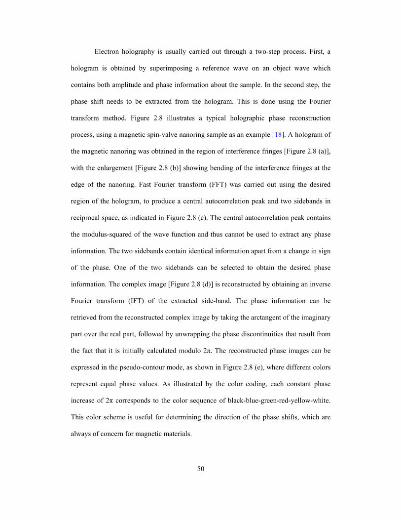
50
ied out using the desired
region o
Electron holography is usually carried out through a two-step process. First, a
hologram is obtained by superimposing a reference wave on an object wave which
contains both amplitude and phase information about the sample. In the second step, the
phase shift needs to be extracted from the hologram. This is done using the Fourier
transform method. Figure 2.8 illustrates a typical holographic phase reconstruction
process, using a magnetic spin-valve nanoring sample as an example [18]. A hologram of
the magnetic nanoring was obtained in the region of interference fringes [Figure 2.8 (a)],
with the enlargement [Figure 2.8 (b)] showing bending of the interference fringes at the
edge of the nanoring. Fast Fourier transform (FFT) was carr
f the hologram, to produce a central autocorrelation peak and two sidebands in
reciprocal space, as indicated in Figure 2.8 (c). The central autocorrelation peak contains
the modulus-squared of the wave function and thus cannot be used to extract any phase
information. The two sidebands contain identical information apart from a change in sign
of the phase. One of the two sidebands can be selected to obtain the desired phase
information. The complex image [Figure 2.8 (d)] is reconstructed by obtaining an inverse
Fourier transform (IFT) of the extracted side-band. The phase information can be
retrieved from the reconstructed complex image by taking the arctangent of the imaginary
part over the real part, followed by unwrapping the phase discontinuities that result from
the fact that it is initially calculated modulo 2π. The reconstructed phase images can be
expressed in the pseudo-contour mode, as shown in Figure 2.8 (e), where different colors
represent equal phase values. As illustrated by the color coding, each constant phase
increase of 2π corresponds to the color sequence of black-blue-green-red-yellow-white.
This color scheme is useful for determining the direction of the phase shifts, which are
always of concern for magnetic materials.
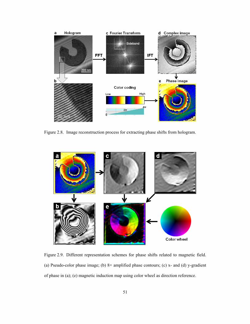
Figure 2.8. Image reconstruction process for extracting phase shifts from hologram.
Figure 2.9. Different representation schemes for phase shifts related to magnetic field.
(a) Pseudo-color phase image; (b) 8× amplified phase contours; (c) x- and (d) y-gradient
of phase in (a); (e) magnetic induction map using color wheel as direction reference.
51

52
For convenience, in order to clarify information about the magnetic field,
including amplitude and direction, several different schemes are used for magnetic
imaging representation, including pseudo-color phase image, amplified black-white phase
contours, and colored magnetic induction map, as shown in Figures 2.9 (a), (b), and (e),
respectively.
For pseudo-color phase images, colors represent the amplitudes of the phase,
while the sequence of colors indicates the direction of phase increase (or decrease) for
determining the magnetization directions based on the right-hand rule. In this particular
example, the phase increases from the inner edge to the outer edge of the ring, indicating
that the magnetization is in a counterclockwise (CCW) rotation. The phase image can be
mplifying the phase, so that the contours indicate the magnetization distribution and the
black-white separation quantifies the amplitude. Although this does not show the
magnetization direction, this straightforward method has been widely used and accepted
by researchers in this field. Another representation, the so-called magnetic induction map,
has also been developed to indicate magnetization directions based on a red-green-blue
(RGB) color wheel scheme. Magnetization components along x and y directions can be
obtained by taking derivatives with respect to the corresponding normal orientations, as
shown in Figure 2.9 (c) and (d). The vector field is then reconstructed by combining the
two orthogonal gradients, and encoding with specific RGB colors. This color scheme is
also widely accepted in the magnetics community, but one drawback is the lack of
amplitude information. Nevertheless, one can take advantage of these last two
representation schemes by coloring the amplified phase contours using the RGB color
wheel. These different schemes are equivalent, and they have all been used in this
dissertation depending on the specific purpose of a particular situation.
represented in grey-scale phase contours by applying a cosine function and then
a
53
ecimen plane is obtained by tilting the sample holder, as shown in Figure
2.10 (a)
specimen height.
In practice, the electron holography observations of nanomagnets in this
dissertation research have been performed in the Lorentz mode using the Philips-FEI
CM200-FEG TEM. An in situ magnetic field can be applied to the specimen by partially
turning on the current of the objective lens, and the desired component of the applied
field in the sp
. The magnetization of the sample can be saturated by tilting the holder by ±30°,
with the in-plane component suitably chosen to exceed the coercive field of the magnetic
layer(s) of interest. The remanent states can then be reached by tilting back to the
horizontal position. To determine a complete hysteresis loop, a series of observations
should be carried out by tilting from +30° to -30° and back to +30°. At each tilt position,
the overall magnetization of the entire element is calculated by taking the integral of the
local magnetization along the in-plane applied field direction using dedicated scripts
written in Gatan Digital Micrograph™. Before calculation, the applied field direction
(tilting direction) for the phase images should be aligned to be horizontal and all of the
images need to be adjusted to the original aspect ratio to ensure that foreshortening or
stretching caused by tilting have no influence on the subsequent processing. The
gradients of the phase shifts perpendicular to the applied field direction are then
calculated for each pixel. The slopes are averaged over the whole element for each tilt
with the background and element edges masked out, where the values for the ±30° tilts
corresponding to full saturation are defined as unity for the M/Ms plot. These values are
then used to normalize the others obtained at different tilts. Thus, the entire hysteresis
loop for in-plane magnetization reversal can be quantitatively determined.
The magnitude of applied magnetic field is based on the prior calibration of the
field as a function of objective lens current, as shown in Figure 2.10 (b). The field is
parallel to the incident beam direction and is not sensitive to changes in

54
The default value for objective lens current in normal operating mode is ~9880 mA,
corresponding to a vertical magnetic field of ~1.90 T (19000 Oe). The residual field at
the specimen plane is unaffected by excitation of the Lorentz minilens, and negligible in
most cases.
Several important parameters need to be considered for holographic imaging,
including fringe spacing, fringe overlap, fringe visibility (contrast), and field of view
[12]. These parameters can be controlled by suitable combinations of accelerating
voltage, extraction voltage, and biprism voltage. To ensure coherent illumination, the
microscope is usually operated at 200 kV with gun lens 5 and spot size 1 setup. The
fringe visibility is quite sensitive to the extraction voltage, with the optimum value of
~3.78 kV. The biprism voltage determines both the fringe spacing and the region of
Figure 2.10. (a) Schematic diagram showing the use of specimen tilt to provide the in-
plane component of the applied field needed for in situ magnetization reversal
experiments. (b) Hall probe measurements of magnetic field in specimen plane of Philips
CM200 as function of objective lens current [2].

overlap, and is typically biased to a potential of 100 V. The holographic fringe contrast is
defined by
minmax
minmax II −=μ (2.8) II +
where I
The term “spin ice” refers to a magnetic system with geometrical frustrated
interactions, where the local disorder of magnetic moments appears in the ordered lattice
structure [19]. Recent experiments have provided evidence suggesting the existence of
deconfined magnetic monopoles in these materials, with properties analogous to the
hypothetical magnetic monopoles postulated to exist in vacuum [20–26].
max and Imin are maximum and minimum intensity, respectively, in the region of
overlap of the interference fringes. The contrast can be measured by an averaged line
profile across the fringes, and typical fringe contrast of ~40% can be obtained, which is
more than adequate for holographic imaging and phase reconstruction.
2.5. Examples of Quantitative Phase Imaging
2.5.1. Kagome lattices
Figure 2.11. (a) In-focus, and (b) defocused, Lorentz TEM image of kagome structure.
Fresnel contrast indicates clockwise and counterclockwise closed loops. [27].
55

56
f an artificial spin ice system using a two-dimensional (2D) kagome lattice
[27]. Lorentz imaging was used to demonstrate the local ice r
occurrence of long-range dipolar interactions, as illustrated by Figure 2.11. However,
conventional EBL
technique, followed by metal deposition of Py (Ni80Fe20) and lift-off [27]. The designed
erent lengths and widths, and separated
ctions. The Py layer is nominally 23 nm in thickness.
the top-right to
the bottom-left direction, and then reverse saturated along the opposite direction.
Holograms in the two opposite remanent states were thus obtained. The corresponding
reconstructed phase images are shown in Figure 2.12 (a) and (b). Line profiles from the
same regions but in opposite magnetic states are shown plotted, and the linear slopes
caused by the magnetic fields only appear at the central part of the wire. However, these
are smeared out at the wire edges due to the nonuniform thickness (or MIP) contribution.
A phase image showing the pure magnetic component could be achieved by the
t constant
Cumings and his group at the University of Maryland have recently described
realization o
ule and as well as the
many details remain to be determined about this topic. As a collaborative project,
electron holography was used to characterize some typical spin-ice samples. These results
also represent an example of quantitative phase imaging.
The kagome-structured spin ice samples were fabricated using
patterns included hexagonal honeycombs with diff
three-fold “Y” shaped jun
The kagome lattice having ~1μm diagonal separation and ~110nm lattice width
was first observed, as shown in Figure 2.12. Because of the limited region of coherent
illumination for electron holography, only the edges of the kagome lattice could be
observed, but some irregular branch shapes were present in such regions due to errors
during fabrication. The initial saturation magnetic field was applied from
subtraction of images, as shown in Figure 2.12 (c). Line profiles indicate a linear slope
across the entire wire, but the slope remains flat elsewhere, suggesting tha

Figure 2.12. Phase images of kagome lattice composed of Py and corresponding line
profiles in remanent state with: (a) saturation field pointing to bottom-left; (b) saturation
field pointing to top-right; and (c) pure magnetic contribution. (d) 8× amplified phase
contours, (e) magnetic induction map, and (f) magnetic contour map, converted from (c).
57

58
magnetization is uniformly distributed within the wire, and that any edge effects have
been completely removed. Measurements showed that the slope of the phase shifts in all
three wires was 0.035±0.001 rad/nm. Since the thickness of the lattice is nominally 23
nm, the corresponding magnetic induction is calculated to be 1.00±0.03 T, which is a
reasonable value for the saturation magnetization of Py. The phase image was converted
into phase contours, magnetic induction map, and magnetic contour map, as shown in
Figure 2.12 (d)–(f), respectively. These clearly indicate the directions of magnetization
and the surrounding fringing fields.
At this junction of the kagome lattice, the magnetic flux comes “in” from the top-
right, and then goes “out” through the left and bottom-right, thus forming an “in-out-out”
configuration. The 2D mapping of the magnetic phase contours within lattice wires and
the external fringing fields confirmed that the magnetization contours were continuous,
and in closure loops, indicating that no magnetic monopoles were present in this area.
Similar characterization was carried out on another kagome lattice with smaller
dimensions of ~500 nm across the diagonal and ~65 nm in lattice width. The
corresponding phase images and magnetic induction maps are shown in Figure 2.13. The
magnetic induction map in Figure 2.13 (b) clearly shows four junctions with different
configurations, where one “in-out-out” configuration (I) is associated with three “in-in-
out” configurations (II, III, and IV). However, only magnetic flux closures, but no
evidence for monopoles, were found in the kagome lattice.

Figure 2.13. Phase contour map (12× amplified), magnetic induction map, and magnetic
contour map of (a)–(c) 500-nm-diagonal kagome lattice, and (d)–(f) enlarged box area,
respecti
and residual chemicals, were
isible on the nitride membrane. These could cause considerable noise in both imaging
and reconstruction of the phase shifts. The boxed area was placed in the region of
coherent illumination and a hologram was obtained, as shown in Figure 2.14 (b). The
reconstructed phase contour map, magnetic induction map, and magnetic contour map are
shown in Figures 2.14 (c)–(e), respectively. Noise signals caused by the contamination,
vely. Magnetization directions indicated by color wheel.
Individual Y-junctions with a 3-fold symmetry shape were observed in order to
investigate any differences in properties between separated junctions and junctions in a
continuous lattice. Figure 2.14 (a) shows the Lorentz image of as-fabricated Y junctions.
Each branch of the Y-junction is 100 nm in width and 400 nm in length. Contaminations
from EBL and lift-off processes, such as metal particles
v
59

60
appearing as big dots or vortices in the phase contour map, did not obscure the result that
the individual Y-junction was in an “in-in-out” configuration, with continuous magnetic
flux.
Although no obvious evidence was found in these studies to confirm the
existence of magnetic monopoles, this investigation of kagome lattices demonstrated the
capability of electron holography for observing and quantifying static magnetic fields on
the nanometer scale.
Figure 2.14. (a) Lorentz TEM image of as-fabricated Y-junctions. (b) Hologram of an
individual Y-junction in boxed area of (a). (c) Phase contour map (12× amplified), (d)
magnetic induction map, and (e) magnetic contour map, respectively, of the Y-junction.
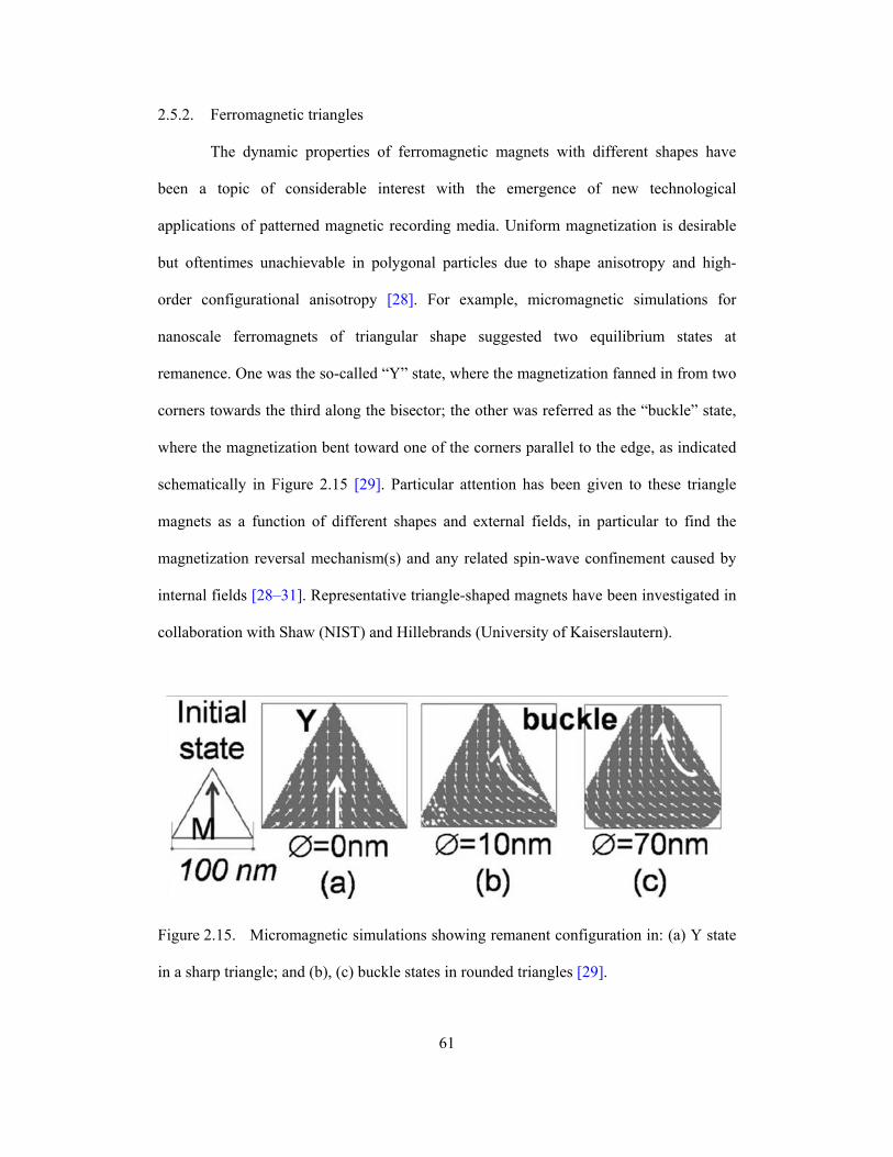
61
a topic of considerable interest with the emergence of new technological
applicat
ets of triangular shape suggested two equilibrium states at
remanence. One was the so-called “Y” state, where the magnetization fanned in from two
corners towards the third along the bisector; the other was referred as the “buckle” state,
where the magnetization bent toward one of the corners parallel to the edge, as indicated
schematically in Figure 2.15 [29]. Particular attention has been given to these triangle
magnets as a function of different shapes and external fields, in particular to find the
magnetization reversal mechanism(s) and any related spin-wave confinement caused by
internal fields [28–31]. Representative triangle-shaped magnets have been investigated in
collaboration with Shaw (NIST) and Hillebrands (University of Kaiserslautern).
2.5.2. Ferromagnetic triangles
The dynamic properties of ferromagnetic magnets with different shapes have
been
ions of patterned magnetic recording media. Uniform magnetization is desirable
but oftentimes unachievable in polygonal particles due to shape anisotropy and high-
order configurational anisotropy [28]. For example, micromagnetic simulations for
nanoscale ferromagn
Figure 2.15. Micromagnetic simulations showing remanent configuration in: (a) Y state
in a sharp triangle; and (b), (c) buckle states in rounded triangles [29].

62
bricated using standard EBL and etching methods. The
patterne
electron
hologra y has been demonstrated to provide useful insights for both static and dynamic
aspects of nanoscale magnetic materials.
The Py triangles were fa
d elements were all of the same thickness of 10 nm, but with different lateral
dimensions, nominally, 1×1.5, 1×1, 0.5×1.5, 0.5×1 (base × height, unit in µm), as shown
by the Lorentz TEM images in Figures 2.16 (a)–(d), respectively.
Each of the magnetization states of these elements during an entire hysteretic
switching process was recorded at a series of tilting positions with respect to the vertical
applied magnetic field. Figure 2.16 shows seven different states (1–7) for each triangle
(a–d) as a function of applied field strength. The two proposed states were identified,
with the buckle states visible at the remanence (a4, b4, c4, d4), whereas the Y states
occurred at the saturation fields (a7, b7, c7, d7). These results are in good agreement with
recent experimental and simulated results [29–31], although the proposed vortex mode
was not observed. Moreover, it was found that the critical fields for the transitions
between the two states varied depending on the different height-base ratios, which most
likely correlates with the shape and configurational anisotropy. Comprehensive
investigation for a better understanding is ongoing, but it can be concluded that
ph

Figure 2.16. Lorentz images of Py triangles with different sizes, and corresponding
phase contours (4× amplified) as function of in-plane applied field. Applied field along
the long axis of the triangles.
63

64
Referen s
[1] . A. McCord and M. J. Rooks, in Handbook of Microlithography, Micromachining, and Microfabrication Volume 1, edited by P. Rai-Choudhury,
PIE Optical Engineering Press, Bellingham, WA, Chapter 2, (1997).
[2] . E. Dunin-Borkowski, M. R. McCartney, B. Kardynal, M. R. Scheinfein, and D. J. Smith, J. Microsc. 200, 187 (2000).
[3] T. Schrefl, D. Suess, G. Hrkac, M. Kirschner, O. Ertl, R. Dittrich, and J. Fidler, in Advanced Magnetic Nanostructures, edited by D. J. Sellmyer and R. Skomski, Springer, New York, Chapter 4, (2006).
[4] T. L. Gilbert, Phys. Rev. 100, 1243 (1955).
[5] L. D. Landau and E. M. Lifshitz, Phys. Z. Sowietunion 8, 153 (1935).
[6] M. J. Donahue and D. G. Porter, OOMMF User's Guide Version 1.0, National Institute of Standards and Technology, Gaithersburg, MD (1999).
[7] J. N. Chapman, J. Appl. Phys.: D 17, 623 (1984).
[8] J. N. Chapman and A. K. Petford-Long, in Magnetic Microscopy of Nanostructures, edited by H. Hopster and H. P. Open, Springer-Verlag, Berlin-Heidelberg, Chapter 4, (2005).
[9] D. Shindo and T. Oikawa, Analytical Electron Microscopy for Materials Science, Springer-Verlag, Tokyo, Chapter 5, (2002).
[10] D. Gabor, Nature 161, 777 (1948).
[11] D. Gabor, Proc. Roy. Soc. London A197, 454 (1949).
[12] D. J. Smith and M. R. McCartney, in Introduction to Electron Holography, edited by E. Völkl, L. F. Allard and D. C. Joy, Kluwer Academic-Plenum Publishers, New York, Chapter 4, (1999).
[13] R. E. Dunin-Borkowski, M. R. McCartney, and D. J. Smith, in Encyclopedia of
Stevenson Ranch, CA, Chapter 7, (2004).
[14] M. R. McCartney and D. J. Smith, Annu. Rev. Mater. Res. 37, 729 (2007).
[15] H. Lichte, P. Formanek, A. Lenk, M. Linck, C. Matzeck, M. Lehmann, and P. imon, Annu. Rev. Mater. Res. 37, 539 (2007)
[16] . Tonomura, Surf. Sci. Rep. 20, 317 (1994).
[17] . E. Dunin-Borkowski, T. Kasama, A. Wei, S. L. Tripp, M. J. Hӱtch, E. Snoeck, nis, Microsc. Res. Tech. 64, 390 (2004).
ce
M
S
R
Nanoscience and Nanotechnology, edited by H. S. Nalwa, American Scientific
S
A
RR. J. Harrison, and A. Put

65
. McCartney, N. Agarwal, S. Chung, D.A. Cullen, M.-G. Han, K. He, L. Li, H. Wang, L. Zhou, D.J. Smith, Ultramicroscopy 110, 375 (2010).
[20] R. F. Wang, C. Nisoli, R. S. Freitas, J. Li, W. McConville, B. J. Cooley, M. S.
ature Phys. 5, 258 (2009).
, K. Kiefer, S. Gerischer, D. Slobinsky, and R. S. Perry, Science 326, 411 (2009).
[26] T. Fennell, P. P. Deen, A. R. Wildes, K. Schmalzl, D. Prabhakaran, A. T.
[27] Y. Qi, T. Brintlinger, and J. Cumings, Phys. Rev. B 77, 094418 (2008).
. Welland, J. Appl. Phys. 88, 5315 (2000).
[29] L. Thevenard, H. T. Zeng, D. Petit, and R. P. Cowburn, J. Appl. Phys. 106,
[31] F. Montoncello and F. Nizzoli, J. Appl. Phys. 107, 023906 (2010).
[18] M.R
[19] L. Pauling, J. Am. Chem. Soc. 57, 2680 (1935).
Lund, N. Samarth, C. Leighton, V. H. Crespi, and P. Schiffer, Nature 439, 303 (2006).
[21] C. Castelnovo, R. Moessner, and S. L. Sondhi, Nature 451, 42 (2008).
[22] O. Tchernyshyov, Nature 451, 22 (2008).
[23] L. D. C. Jaubert and P. C.W. Holdsworth, N
[24] M. J. P. Gingras, Science, 326, 375 (2009).
[25] D. J. P. Morris, D. A. Tennant, S. A. Grigera, B. Klemke, C. Castelnovo, R. Moessner, C. Czternasty, M. Meissner, K. C. Rule, J.-U. Hoffmann
Boothroyd, R. J. Aldus, D. F. McMorrow, and S. T. Bramwell, Science 326, 415 (2009).
[28] D. K. Koltsov, R. P. Cowburn, and M. E
063902 (2009).
[30] M. Jaafar, R. Yanes, A. Asenjo, O. Chubykalo-Fesenko, M. Vázquez, E. M. González, and J. L. Vicent, Nanotechnology 19, 285717 (2008).

CHAPTER 3
66
ORTEX-CONTROLLED
This chapter describes the electron holography investigation of remanent states
and magnetization reversal of monolayer Co nanorings, with and without slots. Vortex-
controlled switching behavior has been identified, which exhibits stepped hysteresis
on states, vortex states, flux-closure
due to their potential applications in high density data storage
for recording
urposes. As the lateral dimensions of the elements are scaled down to the hundreds to
ns of nanometers, their geometry plays an even more important role in determining the
magnetization configuration [4]. Designs based on simple shapes, such as squares,
rectangles, and other polygons, are not really suitable for data storage due to the
occurrence of irregular edge domains [4–7]. Circular disks can lead to stable
magnetization configurations, i.e., flux-closure (FC) states (often refereed to as vortices),
MAGNETIZATION CONFIGURATIONS AND V
SWTICHING BEHAVIOR OF Co NANORINGS
loops with specific well-defined states including oni
states, and omega states. Two distinct switching mechanisms, depending on the applied
field direction relative to the slot orientation, can be attributed to the vortex chirality and
shape anisotropy. Micromagnetic simulations have also been performed to confirm the
experimental observations. The major results of this study have been published elsewhere
[1, 2].
3.1. Introduction
Nanopatterned ferromagnetic (FM) elements have been intensively studied
during the past decade
technology [3]. A reproducible magnetization reversal process with well-defined
remanent states and narrow switching fields is obviously preferable
p
te

67
without any stray field, which thus minimizes any interaction between elements.
However, the presence of the central vortex limits their functionality by complicating the
switching process [8, 9].
Ring-shaped nanostructures are attracting interest because their circular geometry
can sup
out a slot [16–20]. In either of these geometries, the asymmetrical shape leads
predom antly to the onion-FC-onion transition via the formation and annihilation of
DWs. Local spin-vortex structures often appear during the magnetization reversal,
resulting in irregularities in the switching process and broadening of the switching field
distribution. Thus, better understanding and more precise control of the dynamics of
magnetic vortex structures are essential in order to improve the functionality of magnetic
nanostructures [13, 21–22]. Based on micromagnetic simulations, a vortex-dependent
magnetization process with a three-step hysteresis loop was proposed, which suggested
that spin-vortex structures had caused the transform from onion state to FC state [15].
However, no direct experimental evidence for this three-step reversal mechanism has
been previously reported.
In this chapter, Co nanomagnets with ring shapes were chosen for investigation,
where the slots were intended to introduce geometrical restrictions that would change the
port FC states, as well as eliminating the high-energy central vortex core that
causes irreproducibility during magnetization reversal [10–12]. Another common state
obtained in ring structures after saturation is the so-called “onion” or “bi-domain” state,
consisting of two semicircular head-to-head (HTH) domains separated by domain walls
(DWs) [13]. The switching process then occurs out via two different modes, namely,
coherent onion rotation or onion-FC-onion transition [14–16]. Several approaches have
been used to obtain controllable switching mechanisms via the introduction of
asymmetrical characteristics to the ring, including displacement of the central hole or
cutting
in
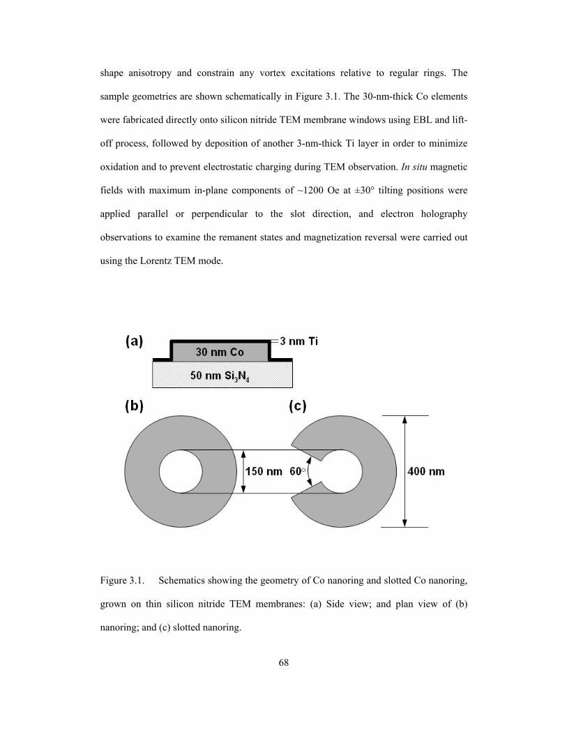
68
to silicon nitride TEM membrane windows using EBL and lift-
off proc
shape anisotropy and constrain any vortex excitations relative to regular rings. The
sample geometries are shown schematically in Figure 3.1. The 30-nm-thick Co elements
were fabricated directly on
ess, followed by deposition of another 3-nm-thick Ti layer in order to minimize
oxidation and to prevent electrostatic charging during TEM observation. In situ magnetic
fields with maximum in-plane components of ~1200 Oe at ±30° tilting positions were
applied parallel or perpendicular to the slot direction, and electron holography
observations to examine the remanent states and magnetization reversal were carried out
using the Lorentz TEM mode.
the geometry of Co nanoring and slotted Co nanoring,
grown on thi
nanoring; and (c) slotted nanoring.
Figure 3.1. Schematics showing
n silicon nitride TEM membranes: (a) Side view; and plan view of (b)

3.2. Remanent States and Switching Behavior of Co Nanorings
The as-prepared Co nanorings were observed with and without applied magnetic
field. Figure 3.2 (a) is a Lorentz image showing the nanorings with outer diameter of
~400 nm and inner diameter of ~150 nm. These nanorings were patterned into 3×3
arrays, with ~800-nm spacing between adjacent elements to minimize any interactions.
The reconstructed phase image of a Co nanoring observed at remanence is shown in
Figure 3.2 (b). Phase shifts due to the magnetic contributions were extracted using a pair
of holograms having opposite FC chirality, as shown in the contour map. The uniformly
Figure 3.2. (a) Lorentz TEM image showing Co nanoring array (Scale bar indicates
500 nm). (b) Reconstructed holographic phase image of an individual nanoring showing
re
y color wheel and overlaid arrows.
FC state at manence, with phase contour spacing of π/3. (c) Line profile from A to B.
(d) Experimental, and (e) simulated, magnetic induction maps of the Co nanoring.
Magnetization directions indicated b
69
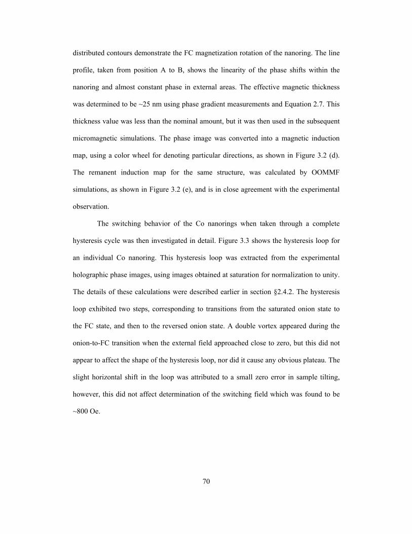
70
The line
profile,
imulations, as shown in Figure 3.2 (e), and is in close agreement with the experimental
observation.
The switching behavior of the Co nanorings when taken through a complete
hysteresis cycle was then investigated in detail. Figure 3.3 shows the hysteresis loop for
an individual Co nanoring. This hysteresis loop was extracted from the experimental
holographic phase images, using images obtained at saturation for normalization to unity.
The details of these calculations were described earlier in section §2.4.2. The hysteresis
loop exhibited two steps, corresponding to transitions from the saturated onion state to
the FC state, and then to the reversed onion state. A double vortex appeared during the
onion-to-FC transition when the external field approached close to zero, but this did not
appear to affect the shape of the hysteresis loop, nor did it cause any obvious plateau. The
slight horizontal shift in the loop was attributed to a small zero error in sample tilting,
distributed contours demonstrate the FC magnetization rotation of the nanoring.
taken from position A to B, shows the linearity of the phase shifts within the
nanoring and almost constant phase in external areas. The effective magnetic thickness
was determined to be ~25 nm using phase gradient measurements and Equation 2.7. This
thickness value was less than the nominal amount, but it was then used in the subsequent
micromagnetic simulations. The phase image was converted into a magnetic induction
map, using a color wheel for denoting particular directions, as shown in Figure 3.2 (d).
The remanent induction map for the same structure, was calculated by OOMMF
s
however, this did not affect determination of the switching field which was found to be
~800 Oe.
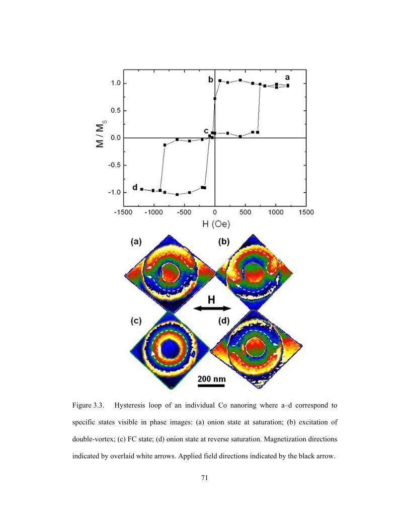
Figure 3.3. Hysteresis loop of an individual Co nanoring where a–d correspond to
pecific states visible in phase images: (a) onion state at saturation; (b) excitation of
ouble-vortex; (c) FC state; (d) onion state at reverse saturation. Magnetization directions
dicated by overlaid white arrows. Applied field directions indicated by the black arrow.
s
d
in
71

72
Figures 3.3 (a)–(d) show representative phase images corresponding to the
magnetization states observed at different stages of the hysteresis loop, which are labeled
with a–d. These configurations were obtained from one half of the hysteresis loop, and
are opposite to those observed in the other half of the loop. The saturation configurations
with strong fringing fields corresponded to the onion state and the reversed onion state, as
shown in Figures 3.3 (a) and (d), respectively. By taking the color sequences into
account, the directions of magnetization can be determined, as indicated by the overlaid
arrows. Two vortices, both with clockwise (CW) chirality, were identified close to the
domain wall (DW) region of the onion configuration, as visible in Figure 3.3 (b). The
chirality of the vortex directly affects the evolution of the vortex and determines the
switching mechanism, as will be discussed in detail later. The double-vortex state was
formed as the external field approached the remanence condition, and it was then
eliminated leaving behind a flux-closure state with CW magnetization and minimal
fringing field, as shown in Figure 3.3 (c). The upper half of the element reversed first to
form the FC, followed by switching of the lower half to obtain the completely reversed
onion state. The presence of the FC configuration was visible as a flat plateau, and
stabilized the Co nanorings.
3.3. Remanent States and Switching Behavior of Slotted Co Nanorings
As-prepared Co slotted nanorings were observed with and without applied
magnetic field. Figures 3.4 (a) and (b) show Lorentz images of two sets of element arrays
with the slot orientations rotated by 90°. The in-plane magnetic field was applied along
the directions indicated by arrows, i.e., parallel to the slot direction in Figure 3.4 (a), and
perpendicular to the slot direction in Figure 3.4 (b). For convenience, the designations
SR1 and SR2 will be used to denote slotted rings with slot directions parallel, or

73
perpendicular, to the applied field direction, respectively. Typical elements in both arrays
were observed at the remanent state after initial saturation and removal of the applied
field, and the corresponding reconstructed phase images are shown in Figures 3.4 (c) and
(d). Observations showed that the remanent magnetization configurations exhibited onion
states when the initial saturation field was applied parallel to the slot orientation, whereas
FC states were preferentially obtained with the initial saturation direction perpendicular
to the slot direction.
Figure 3.4. Lorentz images of Co slotted nanorings, with slot directions (a) parallel,
and (b) perpendicular, to applied field directions (indicated by double arrow).
Reconstructed phase images showing individual Co elements at remanence: (c) onion;
and (d) FC state.

74
The switching behavior of the Co slotted nanorings through a complete hysteresis
cycle was also observed. Figure 3.5 compares hysteresis loops for Co nanorings with in-
plane field applied parallel, and perpendicular, to the slot direction. The inset schematics
indicate the different magnetization configurations of each state that occur during the
hysteresis cycle. For the shape SR1 with external field applied parallel to the slot, as
shown in Figure 3.5 (a), the hysteresis loop exhibited three steps, corresponding to
transitions between saturated onion state, vortex excitation, FC state, and reversed onion
state. Conversely, when the external field was applied perpendicular to the slot direction,
as shown in Figure 3.5 (b), the shape SR2 exhibited a simple one-step hysteresis loop
with good squareness, indicating that the magnetization of the slotted ring reversed
abruptly between FC states of opposite chirality. The switching fields were determined to
be ~800 Oe for the shape SR1 and ~700 Oe for the shape SR2. It is noteworthy that the
three-step hysteresis loop had been predicted by numerical simulations for ring-shaped
Py elements with similar dimensions [15]. However, these experimental results are the
first time that such evidence has been observed for Co slotted-ring elements.
Figure 3.6 shows representative phase images corresponding to the states at
different stages of the hysteresis loop labeled a–d in Figure 3.5 (a). The saturation
configurations corresponded to the onion state and the reversed onion state with strong
fringing fields, as shown in Figures 3.6 (a) and (d), respectively. As indicated by the
overlaid arrows, the magnetization direction in Figure 3.6 (a) was counterclockwise
(CCW) in the upper half of the nanoring, and CW in the lower half, and vice versa in
Figure 3.6 (d). A vortex with CCW chirality was identified close to the domain wall
region of the onion configuration, as visible in Figure 3.6 (b). The precise location of this
vortex formation could be related to local defects of the sample or possible geometrical
asymmetry between the two branches. The vortex was formed as the external field

75
Figure 3.5. (a) Three-step, and (b) one-step, hysteresis loops for Co elements with
applied field parallel, and perpendicular, to the slot direction, respectively. The inset
schematics indicate the different magnetization configurations that occurr during the
hysteresis cycle.

76
Figure 3.6. Phase images of Co nanoring (SR1) illustrating the magnetization
configurations for corresponding states in the hysteresis loop in Figure 3.5 (a): (a) onion
state; (b) excitation of vortex at remanence; (c) FC state; and (d) reversed onion state.
Figure 3.7. Phase images of Co nanoring (SR2) illustrating the magnetization
configurations for corresponding states in the hysteresis loop shown in Figure 3.5 (b): (a)
Ω state; (b) FC state of CW; (c) FC state of CCW; and (d) reversed Ω state.

77
approached the remanence condition, and it was then eliminated leaving behind a flux-
closure state with CW magnetization and a weak fringing field, as shown in Figure 3.6
(c). The upper half of the element reversed first to form the FC state, followed by
switching of the lower half to complete the FC-to-onion transition. The presence of the
FC configuration stabilized the Co element, visible as a flat plateau, which was also
responsible for the increase of the switching field to ~800 Oe, relative to ~700 Oe for the
shape SR2. Micromagnetic simulations indicated that the transition from onion state to
FC state was dependent on the evolution of the vortex. Once the vortex was formed, it
could move in two alternative directions: either it would take the shorter route to the end
of the associated branch, or else take the longer route towards the other end. Meanwhile,
that branch also reversed its magnetization to reach the flux-closure state. The shorter
distance would be preferable, although the other case could occasionally occur, as
indicated in Figure 3.6 (c).
Figure 3.7 shows phase images corresponding to the states labeled a–d in the
hysteresis loop of Figure 3.5 (b). When the field was applied perpendicular to the slot
direction, the saturation configurations of shape SR2 appeared as “Ω” states, which were
FCs with magnetization twisted to the direction of the external field at the slot edges, as
shown in Figures 3.7 (a) and (d). As the applied field was reduced below the coercivity
(~700 Oe), the magnetization relaxed to form a FC state with CW chirality, as visible in
Figure 3.7 (b). When the applied field was decreased further to a negative coercivity
value, the magnetization of the slotted ring reversed abruptly from the CW FC state to the
CCW chirality, as visible in Figure 3.7 (c).

78
s a more sheared shape than that in Figure 3.8 (c).
3.4. Comparison Between Experimental Results and Simulations
Micromagnetic simulations were systematically performed for both experimental
geometries of regular and slotted rings, with external fields applied parallel or
perpendicular to the slot direction, where applicable. The experimental and simulated
results are compared in each situation, and also summarized for all three shapes of ring,
SR1, and SR2. Figures 3.8 (a)–(c) show the hysteresis loops obtained from experimental
electron holograms of the nanoring, and shapes SR1 and SR2, respectively. The coercive
fields were determined by averaging the values from both forward and backward cycles
of each specific element, as summarized in Table I. Simulated hysteresis loops from
micromagnetic modeling for the ring, SR1, and SR2, are shown in Figures 3.8 (d)–(f),
respectively. From comparisons between the corresponding loops, it is apparent that the
experimental and simulated results are in close quantitative agreement, except that the
loop in Figure 3.8 (f) exhibit
Table 3.1. Switching fields measured from experimental and simulated hysteresis loops.
Switching fields (Oe) Sample
Experimental Simulated
Ring ~800 950±50
SR1 ~800 800±100
SR2 ~700 850±50

Figure 3.8. (a)–(c) Experimental, and (d)–(f) simulated, hysteresis loops for Co
anoring, slotted nanoring with applied field parallel to slot (SR1), and slotted nanoring
ith applied field perpendicular to slot (SR2), respectively.
n
w
79

80
The primary difference in behavior between these three geometries is that shape
SR2 shows a one-step hysteresis loop, whereas shape SR1 and the regular nanoring
exhibit multiple steps in their loops. These steps represent transitions between distinct
and well-defined magnetization configurations, including onion state, vortex formation,
and FC state. Moreover, because the occurrence of these steps corresponds to different
fields, the elements show different remanent configurations. The representative states, as
indicated by letter labels, are illustrated in Figure 3.9: the magnetization configurations,
and colors (denoting directions), for the corresponding pairs of measured and simulated
images are in excellent agreement. Detailed information about the behavior observed for
each specific geometry has already been given. However, it is useful to compare the
magnetization reversal and vortex evolution, which were most often observed in
numerous experiments for the different shapes.
For the regular ring shape, when the strength of the applied field is decreased
from initial saturation, vortices gradually form at the DW regions to minimize the total
energy via reduction of the fringing field. A double-vortex (1b and 1f) forms within the
onion configuration, when the field is close, but not equal, to zero. These two vortices,
having the same CCW chirality, move toward each other, and then annihilate to form a
simple CCW FC state at remanence (1c and 1g). Eventually, the FC state becomes a
reverse onion state by reversal of the lower half-ring after the field exceeds the switching
value (1d and 1h). This latter transition took place too quickly to catch any intermediate
states during the observation. Thus, the overall magnetization switching process takes
place via the onion-FC-onion mechanism, which is consistent with previous numerical
simulations and experimental observations [14, 17].

Figure 3.9. Magnetic induction maps for (1) Co ring, (2) SR1, and (3) SR2, comparing
corresponding states in Figure 3.8. Applied field along horizo
the experimental results (upper row) and simulations (lower row). Letter labels refer to
ntal direction. Contour
spacing of π/2. Magnetization directions indicated by color wheel or overlaid arrows.
81

82
The SR1 shape exhibits an onion state at saturation (2a and 2e), and undergoes an
onion-FC-onion switching behavior, which is similar to that of the regular ring, because
both shapes are symmetrical with respect to the applied field direction. However, since
the presence of the slot breaks the horizontal symmetry in the region where a vortex is
expected, only one vortex is formed at remanence during the onion-to-FC transition, as
was indicated in images 2b and 2f. This single vortex, with clockwise (CW) chirality,
moves downward through the entire lower half-branch, and then annihilates at the slot
edge to form the CW FC configuration (2c and 2g). The longer path for this single vortex,
which requires more energy from the applied field, provides an explanation for the
postponed FC appearance relative to that observed for the regular nanoring. Finally, the
upper half-branch reverses to reach the reverse onion state (2d and 2h), although no
information has been observed that shows the details of this switching process.
In contrast to the multi-step switching behavior for the elements above, the SR2
shape experiences a simple one-step reversal. The saturation configuration appears as an
Ω-state (3a and 3d), then relaxes into the CCW FC configuration (3b and 3e) as the
applied field is reduced below the coercivity, and retains this state before reversal to the
CW FC state occurs (not shown). The change in geometry causes a shape anisotropy
perpendicular to the applied field direction, which in turn avoids occurrence of the onion
state. However, the Ω-state might be loosely considered as greater than half of the onion
configuration, showing magnetization that is more curved than the normal half-onion.
The chirality reversal of the FC is thus not due to vortex motion from one slot edge to the
other, but most likely involves the vortex that emerges at the lower central part of the
inner ring edge, as indicated in image 3c and 3f, which sweeps downward across the ring.
This result suggests that the FC-to-onion transitions might also be achieved via a similar
process for the nanoring and SR1 samples.

83
3.5.
other side
having t
x would require absolute symmetry of both
Discussion
3.5.1. Effects of vortex chirality on switching mechanisms
Based on these observations for the ring and SR1 samples, it appears that the
vortex chirality is primarily responsible for the direction of vortex movement and which
subsequent configuration is obtained. Thus, a general rule for vortex behavior after onion
states can be proposed as a function of the magnetization chiralities of the vortex and the
semicircular half-onions. For a vortex with specific chirality present between two
semicircular HTH domains, it would be preferable to move toward the half-onion branch
with opposite chirality, and then subsequently to form an FC state with the same chirality,
as illustrated in Figure 3.10. From the phenomenological point of view, a vortex can be
associated with two half-onion branches: on the side having the half-onion of the same
chirality, the magnetization gradually merges into the vortex, whereas on the
he half-onion of the opposite chirality, abrupt changes in direction occur at the
boundary, as indicated by the obvious contrast of colors. Reduction of exchange energy
would require enlargement of regions with similar magnetization, thus leading to the
proposed vortex motion. Under this vortex-motion rule, either switching mode could be
realized in regular rings: onion-FC-onion transition for double-vortex having the same
chirality, and coherent onion rotation for double-vortex having opposite chiralities, as
depicted in Figure 3.10 (b) and (c), respectively. The coherent rotation mode did not
occur in our experiments, due to intentional removal of the slots. However, only the
onion-FC-onion switching mode was identified in regular rings This contrasts with
previously identified cases that showed both modes [14, 17], thus implying strong
dependence of the switching mechanism on the lateral dimensions and thickness of the
element. Theoretical simulations indicate that similar probabilities for occurrence of
either CW or CCW chirality of the vorte

84
Figure 3.10. Schematics showing vortex controlled switching mechanism for nanorings:
(a) vortex motion rule; (b) onion-FC-onion transition; and (c) coherent onion rotation.
element shape and initial magnetization configuration with respect to the in-plane field
direction, almost independent of any out-of-plane field. In practice, due to shape
variations of an actual element and/or the presence of other defects, one particular vortex
chirality would be preferably present and would then predominate during the subsequent
reversal.
3.5.2. Effects of shape anisotropy on switching fields
The shape anisotropy of the elements plays a major role in determining the
transitions during switching, in terms of affecting the demagnetization field and stray
fields around the sample. Since the magnetization was mostly distributed in circular
arrangements, FC states in the regular nanorings with little stray field or demagnetization
field provide the most stable configurations. In contrast, onion states exhibit much larger
stray fields due to magnetization leakage, and have increased demagnetization field
within elements due to surface dipole moments. The FC states in slotted rings are,

85
however, in a situation between the above two states: demagnetization fields slightly
increase due to surface dipoles at the slot, but are still less than those in onion states.
These suppositions have been confirmed by calculation of demagnetization energies for
the Co nanoring and SR1 samples, as shown in Figure 3.11. These OOMMF simulations
also indicate that other energies involved, for example, anisotropy energy and exchange
energy, are much lower (on an order of magnitude scale) than the demagnetization
energy, which is therefore most likely to dominate the switching fields for FC-to-onion
transitions. For example, the FC-to-onion transition in the regular nanoring leads to
ase of de
causes the switching field changes, consistent
greater incre magnetization energy compared to the SR1 shape, and thus results
in higher switching field. Overall, the shape anisotropy affects the demagnetization
energy within the elements, which in turn
with the trends indicated in Table 3.1.
Figure 3.11. Demagnetization energy as a function of applied field for Co nanoring and
SR1 shape, as calculated from OOMMF simulations. The calculation is obtained from the
forward hysteresis half-cycle (from positive field to negative field).

86
3.6. Conclusions
The behavior of Co nanorings and slotted nanorings, with orthogonal magnetic
fields applied with respect to the slot direction, has been investigated using off-axis
electron holography and micromagnetic simulations. The hysteresis loops were
quantitatively measured and well-defined states, i.e., onion states, FC states, and vortex
formation, were identified for different types of elements, also showing excellent
agreement with simulations. The Co nanorings and slotted nanorings with parallel fields
exhibited multi-step switching behavior via onion-FC-onion mode, involving the
formation and annihilation of single- or double-vortex states. The chirality of the vortex
(or vortices) that formed following formation of the onion states was responsible for the
switching mechanism. In contrast, slotted rings with perpendicular fields underwent one-
step switching by abrupt chirality reversal of the FC states. Introduction of the slot caused
shape anisotropy, which in turn affected the switching fields in terms of demagnetization
energy. Overall, it can be concluded that the combination of electron holography with
micromagnetic simulation provides a powerful approach for extracting detailed
information about the switching behavior of nanoscale magnetic elements.

87
[1] 3885 (2009).
[2] K. He, D. J. Smith, and M. R. McCartney, J. Appl. Phys. 107, 09D307 (2010).
[3] C. A. Ross, Annu. Rev. Mater. Res. 31, 203 (2001).
[4] R. P. Cowburn, J. Phys. D 33, R1 (2000).
[5] R. E. Dunin-Borkowski, M. R. McCartney, B. Kardynal, S. S. P. Parkin, M. R.
2] M. Klӓui, C. A. F. Vaz, L. Lopez-Diaz, and J. A. C. Bland, J. Phys.: Condens. Matter 15, R985 (2003).
3] J. Rothman, M. Klӓui, L. Lopez-Diaz, C. A. F. Vaz, A. Beloch, J. A. C. Bland, Z. Cui, and R. Speaks, Phys. Rev. Lett. 86, 1098 (2001).
4] H. Hu, H. Wang, M. R. McCartney, and D. J. Smith, J. Appl. Phys. 97, 054305 (2005).
5] M. F. Lai, C. N. Liao, Z. H. San, C. P. Lee, Y. P. Hsieh, and T. F. Ho, J. Appl. Phys. 103, 07C517 (2008).
6] M. H. Park, Y. K. Hong, S. H. Gee, D. W. Erickson, and B. C. Choi, Appl. Phys. Lett. 83, 329 (2003).
7] F. Q. Zhu, G. W. Chern, O. Tchernyshyov, X. C. Zhu, J. G. Zhu, and C. L. Chien, Phys. Rev. Lett. 96, 027205 (2006).
References
K. He, N. Agarwal, D. J. Smith, and M. R. McCartney, IEEE Trans. Magn. 45,
Scheinfein, and D. J. Smith, J. Microsc. 200, 187 (2000).
[6] T. Schrefl, J. Fidler, K. J. Kirk, and J. N. Chapman, J. Magn. Magn. Mater. 175, 193 (1997).
[7] H. Wang, H. Hu, M. R. McCartney, and D. J. Smith, J. Magn. Magn. Mater. 303, 237 (2006).
[8] R. P. Cowburn, D. K. Koltsov, A. O. Adeyeye, M. E. Welland, and D. M. Tricker, Phys. Rev. Lett. 83, 1042 (1999).
[9] C. A. F. Vaz, L. Lopez-Diaz, M. Klӓui, J. A. C. Bland, T. L. Monchesky, J. Unguris, and Z. Cui, Phys. Rev. B 67, 140405(R) (2003).
[10] S. P. Li, D. Peyrade, M. Natali, A. Lebib, Y. Chen, U. Ebels, L. D. Buda, and K. Ounadjela, Phys. Rev. Lett. 86, 1102 (2001).
[11] S. P. Li, W. S. Lew, J. A. C. Bland, M. Natali, A. Lebib, and Y. Chen, J. Appl. Phys. 92, 7397 (2002).
[1
[1
[1
[1
[1
[1

88
uang, M. A. Schofield, and Y. Zhu, Appl. Phys. Lett. 95, 042501 (2009).
11 (2007).
[21] T. Pokhil, D. Song, and J. Nowak, J. Appl. Phys. 87, 6319 (2000).
[22] J. K. Ha, R. Hertel, and J. Kirschner, Phys. Rev. B 67, 224432 (2003).
[18] L. H
[19] H. Hu, H. Wang, M. R. McCartney, and D. J. Smith, Phys. Rev. B 73, 153401 (2006).
[20] N. Agarwal, M. R. McCartney, and D. J. Smith, J. Appl. Phys. 102, 0239

89
CHAPTER 4
ATION CONFIGURATIONS AND SWTICHING BEHAVIOR OF
This chapter describes investigation of the different remanent configurations and
switching behaviors of multilayer Co/Cu/Py spin-valve slotted nanorings, as a function of
eld direction relative to the slot directions. It was found that the Co and Py
layers can be aligned parallel at saturation and antiparallel at remanence due to the
interlayer coupling. Two-step and three-step hysteresis loops were quantitatively
determined for slots perpendicular, or parallel, to the applied field, respectively.
Magnetization configurations at each stage were directly visualized, and switching
mechanisms were also proposed. The results of these studies have been published
elsewhere [1, 2].
4.1. Introduction
The spin valve (SV) basically consists of two ferromagnetic (FM) layers
separated by a nonmagnetic metallic spacer. The switching fields of the FM layers are
usually different, with one layer being magnetically soft, while the other is either
intrinsically hard or else exchange-pinned to an adjacent antiferromagnetic layer. The
magnetization of the two layers can be switched independently, and thus parallel and
antiparallel coupling can be achieved. The giant magnetoresistance (GMR) of the
multilayers depends on the change in resistance for the relative magnetization directions
of the two layers [3].
Since their discovery in 1986 [4], and because of their useful GMR properties,
MAGNETIZ
Co/Cu/Py SPIN-VALVE SLOTTED NANORINGS
the applied fi

90
spin-valve structures have been intensively studied for technological applications such as
magnetic sensors and magnetic random access memory (MRAM), as well as being of
fundamental interest due to the variety of magnetization states and the strong interactions
between adjacent ferromagnetic layers [5–13]. Micromagnetic simulations have also been
carried out to investigate magnetostatic coupling, magnetization reversal mechanisms,
and dynamic interactions [10–13]. However, experimental visualization of magnetization
distributions for coupled multilayers is still challenging, because most magnetometry
techniques lack the resolution or sensitivity to characterize individual nanostructures or
the capability to provide quantitative information. Lorentz microscopy has been widely
used to characterize the domain structures of monolayer magnetic elements [14].
However, due to the often complicated coupling in spin-valve multilayers, this technique
is not readily capable of interpreting changes in magnetic contrast within multilayer
elements. Off-axis electron holography represents a powerful approach for
characterization of spin-valve structures, because it can measure phase shifts
quantitatively and thus extract unique micromagnetic information.
In this chapter, the Co/Cu/Py (where Py = Ni Fe ) system was selected for the
SV elements, and slotted rings with different outer/inner diameters (OD/ID) and slot
angles (α) were chosen for the SV element shapes, as shown in Figure 4.1. Elements of
different sizes were patterned into 3×3 arrays, with the separation between elements at
least twice the OD, and the separation between arrays even greater, to eliminate any
possibility of magnetostatic interactions. A variety of combinations of geometrical
parameters, with nominal OD/ID of 300/100, 400/100, 400/200, 500/200, 600/200 nm,
and slot angles of 30°, 60°, 90°, were patterned onto the silicon nitride membranes using
standard EBL and lift-off methods (details as described in §2.2).
81 19

Figure 4.1. Schematics illustrating (a) the structure of trilayer stack, and (b) the shape of
slotted ring, for Co/Cu/Py SV elements.
4.2. Magnetization Configurations and Interlayer Coupling at Remanent State
As-prepared elements were observed in the Lorentz TEM mode, with the
magnetic field applied parallel or perpendicular to the slot bisecting direction. Figure 4.2
(a) shows a typical 3×3 element array of SV elements with nominal OD/ID = 400/200 nm
and α = 60° at remanent state (although the actual inner diameter is ~150 nm after
fabrication). Figure 3.2 (b) shows an under-focused Lorentz image, which clearly
displays Fresnel contrast within the elements but differences between the different states
are not easily distinguished. Thus, detailed information about the magnetization behavior
cannot be easily extracted or interpreted using this technique.
91

Figure 4.2. (a) In-focus image showing as-prepared array of Co/Cu/Py SV elements
(OD/ID= 400/200nm, α = 60°); (b) defocused Fresnel image of single Co/Cu/Py SV
ment in remanent state.
Off-axis electron holograms of SV elements at remanent state were recorded, and
several
the applied field direction
was ~1.65 rad across the ring in Figure 4.3 (b). The slightly decreased contour density
and therefore Ms for the element in Figure 4.3 (a) is likely to be due to the stronger
fringing field for the onion state which decreased the net measured magnetic field,
ele
typical reconstructed phase images are shown in Figure 4.3. Based on observations of
arrays of elements, it was found that the onion state was primarily obtained when
the initial in-plane saturation field was applied parallel to the slot direction, as shown in
Figure 4.3 (a), whereas the flux-closure (FC) state was dominant when the saturation
field was applied perpendicular to the slot direction, as visible in Figure 4.3 (b). For
better visualization of the magnetization configurations, equiphase contours have been
superimposed on the phase images, with the contour lines along the direction of magnetic
induction, so that the contour density is then proportional to the magnitude of the
magnetization (Ms). The measured phase shift perpendicular to
92

93
compared with the FC state in (b). In comparison with the phase shifts expected for
monolayer Co slotted rings [15], it was clear that the remanent state of the trilayer
structure was dominated by the magnetically more massive Co layer, as seen previously
for several simple Co/Au/Ni SV trilayer shapes [13], while the occasional presence of
extra vortices (not shown) was likely due to local coupling with the Py layer.
Further quantitative analysis clarified the interactions between the Co and Py
layers at remanent state. Figures 4.4 (a) and (b) show the phase images at remanence after
saturation in opposite directions: these are both FC states, with chirality of
counterclockwise (CCW), and clockwise (CW), respectively. Line profiles were plotted
Figure 4.3. Reconstructed holographic phase images of Co/Cu/Py SV elements
showing different remanent configurations: (a) onion state; (b) FC state. Initial saturation
direction from bottom-left to top-right. Color bar shows phase in images ranging from 0
to 4π. Equiphase contours represent phase shifts due to magnetic induction, with contour
spacing of 0.2 radians.

94
remanence.
Althoug
out at the same positions of the elements, as shown in Figure 4.4 (c). Measurements show
that the slopes of the phase shifts inside the SV elements are -0.0401 rad/nm and 0.0126
rad/nm, corresponding to 2.67 T CCW and 0.84 T CW, respectively. These values are
well matched with the sum and difference of the magnetization of separate Co and Py
layers, indicating that both parallel and antiparallel configurations can exist at
h the antiparallel state should be favored in order to minimize demagnetization
Figure 4.4. Phase images of (a) parallel- and (b) antiparallel-coupled configurations of
slotted SV element at remanent state. (c) Corresponding line profiles after removal of
MIP contributions. Saturation directions indicated by white arrows.

95
creased, this magnetization state became unstable, and parallel-coupled configurations
and/or vortices started to appear, typically when the OD was ≥ 500 nm. In addition,
changing the slot angle from 30° to 90° did not seem to affect remanence very much.
Thus, nanorings with OD/ID of 400/200 nm and slot angle of 60° were chosen for
investigation of typical switching behavior.
4.3. Switching Behavior of Slotted Nanorings
Switching behavior of the SV elements was investigated by a sequence of
specimen tilting in an in situ applied vertical magnetic field. The objective lens current
was slightly turned on and set to ~1000 mA, corresponding to a vertical magnetic field of
~2400 Oe. Thus, an in-plane field with maximum of ~1200 Oe at ±30° tilting positions
could be applied parallel or perpendicular to the slot direction.
4.3.1. Applied field perpendicular to slot direction
Experimental values of the in-plane magnetization within individual SV
nanorings with applied field perpendicular to slot direction were extracted from
reconstructed phase images at different specimen tilting angles and normalized to unity at
s
soft (Py) layer was
energy, the occasional occurrence of parallel states probably illustrates that the switching
field for the Py layer is quite close to remanence.
The effect of the SV element size on remanent configuration was also studied.
Based on observations of several individual elements for each size, it was found that the
remanent states of small elements (OD/ID = 300/100 nm) exhibited stable flux closures
with consistently antiparallel configurations. As the diameter and width of the rings was
in
saturation, u ing the method described in section §2.4.2. Figure 4.5 illustrates entire
hysteresis loops for a specific SV element through a major cycle, where both layers were
completely reversed, as well as a minor cycle, where only the

96
reversals of the Py and Co layers,
respecti
swapped but the hard (Co) layer remained unchanged. The major hysteresis loop
indicated two steps, corresponding to separate
vely. The overlaid schematics indicate the different magnetic coupling between
the two layers: parallel coupled Ω-states at saturation (a and d), antiparallel coupled FC
states (c and f) at remanence, and parallel coupled FC states (b and e) as intermediate
states in between. Figure 4.6 shows representative magnetization configurations
corresponding to states a–c in the forward cycle of the hysteresis loop, and vice versa in
the other half cycle. The Co layer dominated the magnetization change from Ω- to FC-
state, while reversal of the Py layer reduced the contour density. It was found that the
Figure 4.5 Hysteresis loops for Co/Cu/Py SV element through major and minor
cycles. Applied field perpendicular to the slot direction. Insert schematics indicate
different magnetic coupling between Co and Py layers during the hysteresis cycle.

Figure 4.6. Phase contour (4× amplified) images showing representative magnetization
states corresponding to labels a–c in Figure 4.7: (a) parallel coupled Ω-state; (b) parallel
coupled FC; (c) antiparallel coupled FC.
switching field for the Py layer was very close to remanence, which would explain the
observations of both parallel and antiparallel remanent states. The switching fields
needed to reverse both ferromagnetic layers were on the order of 700 Oe, which is
consistent with the coercivity of monolayer Co reported in Chapter 3.
The minor hysteresis cycle, as shown in Figure 4.5, was also performed in order
to examine the switching behavior of the free (Py) layer. The entire minor loop exhibited
a shift with respect to remanence, which is analogous to the exchange bias effect
observed in the ferromagnetic/antiferromagnetic (FM/AFM) system. However, the
direction of shift is along the positive field direction, which is contrary to the negative
shift in the FM/AFM structure. This is due to the interlayer coupling of the underlying
hard Co layer, which provided a biasing field along its saturation direction. The bias
magnetic field was determined to be ~200 Oe, and the coercivity of the Py layer was
measured to be ~150 Oe, corresponding to the half width of the minor loop. This property
of the minor hysteresis loop could prove to be useful for applications of hard disk reading
head, MRAM, and magnetic sensors.
97

98
4.3.2. Applied field parallel to slot direction
The switching behavior of the Co/Cu/Py SV elements through a complete
hysteresis cycle was also investigated for the applied field parallel to the slot direction.
Figure 4.7 illustrates an entire loop measured directly from the experimental holographic
phase images, followed by normalization to unity at saturation, where the slight
horizontal shift of the loop is attributed to a zero error in sample tilting. The different
magnitudes of M/Ms for the upper and lower half of the hysteresis loop is probably
attributable to the shift of the entire hysteresis loop, which is possibly caused by the
residual vertical magnetic field. It is suspected that the decreasing magnitudes of the
plateaus are because the magnetization is gradually rotating away from the saturation
Figure 4.7. Three-step hysteresis loops for Co/Cu/Py SV nanoring with applied
magnetic field parallel to the slot direction. Insert schematics indicate different magnetic
coupling between Co and Py layers with onion configurations during the hysteresis cycle.

99
owever, this decrease is relatively small
compar
alue of ~700 Oe obtained with the field applied perpendicular to the slot.
Figure 4.8 shows representative phase images corresponding to the labels a–h in
different stages of the hysteresis loop in Figure 4.7. Each configuration could be
considered as a combination of onion state and flux closure with parallel or anti-parallel
coupling between the separate Co and Py layers. The parallel-coupled saturation states
and the antiparallel-coupled remanent states of the onion configuration can be identified,
as shown in (a) (e) and (c) (g), respectively. The transition from saturation to remanence
was observed, as shown in (b) and (f). The upper half of the Py layer reversed first to
form a FC state, followed by reversal of the other half, while the Co layer remained in the
onion state. The intermediate states between remanence and reverse saturation were
visualized, as shown in (d) and (h), in which the upper half of the Co layer first switched
from the onion state to flux closure, and then the other half reversed at higher field values
o
state as the applied field starts to be reduced. H
ed with the reversal of layers.
Unlike the two-step hysteresis loop for the SV element with external field applied
perpendicular to the slot direction, this loop exhibited three steps when the field was
applied parallel to the slot. The overlaid schematics indicate the different configurations
of the onion states: parallel-coupled onion states at saturation (a and e) and antiparallel-
coupled onion states (c and g) at remanence, as well as two extra intermediate states (d
and h) consisting of half-parallel-coupled and half-antiparallel-coupled. The occurrence
of these extra intermediate states stabilized the Co layer, in effect delaying its full
reversal until a switching field of ~800 Oe was reached, which is to be compared with the
v
to form the pposite onion state. The results indicate that the Py and Co layers both
performed a two-step switching mechanism: from onion state to FC state and from flux-
closure to reverse onion state.
Figure 4.8. Phase contour (4× amplified) images of SV element illustrating the
magnetization configurations of corresponding states in the hysteresis loop of Figure 4.7.
Applied fields are parallel to the slot direction, horizontally from right to left for (a)–(d),
and from
of the SV structure.
left to right for (e)–(h).
The three-step hysteresis loop can be schematically drawn with regard to the
behavior of the individual Co and Py layers, as shown plotted in Figure 4.9. The lack of
flatness of the plateaus would be due to the gradually reduced alignments of the
magnetization. The Co layer exhibited a two-step hysteresis loop with two plateaus
corresponding to flux-closure states, which is in good agreement with the previous
experimental data from monolayered Co elements. The Py layer showed a simple
hysteresis loop without obvious steps due to the narrow switching field distribution,
although extra steps might be visible if more data could be obtained. It is noteworthy that
the Py layer underwent a reverse clockwise loop, where magnetization reversal occurred
before the remanence condition, unlike normal hysteresis. This behavior is due to the
strong antiparallel coupling with the Co layer, which is magnetically harder, and thus
dominates the overall behavior
100

101
Figure 4.9. (a) Schematic hysteresis loop after Figure 4.7. Magnetic components
separated to represent the individual behavior of (b) Co, and (c) Py layers.
102
.4. Conclusions
The remanent magnetization configurations and switching behavior of Co/Cu/Py
slotted nanoring SV elements as function of applied field direction relative to the slot
orientation have been characterized using off-axis electron holography. At the remanent
condition, the Co and Py layers align in the antiparallel-coupled configuration, with
predominant states in FC or onion states with the applied field perpendicular or parallel to
the slot direction, respectively. The SV nanorings exhibited multi-step switching
mechanisms, which is attributed to intrinsic coercivity difference and magnetic coupling
between the Co and Py layers. When the external field was applied perpendicular to the
slot, the elements underwent a two-step hysteresis loop, corresponding to separate
reversal of Py and Co layer. When the external field was applied parallel to the slot, the
spin valve showed a well-defined three-step hysteresis loop, corresponding to transitions
between saturation, remanence, and intermediate states. In the latter situation, both Co
and Py layers performed a two-step switching mechanism via onion-FC-onion transition.
4
103
[1]
Lett. 57, 2442 (1986).
[5] B. Dieny, V. S. Speriosu, S. S. P. Parkin, B. A. Gurney, D. R. Wilhoit, and D.
2] G. X. Li and S. X. Wang, IEEE Trans. Magn. 39, 3313 (2003).
3] D. J. Smith, R. E. Dunin-Borkowski, M. R. McCartney, B. Kardynal, and M. R. Scheinfein, J. Appl. Phys. 87, 7400 (2000).
4] J. N. Chapman, J. Phys. D: Appl. Phys. 17, 623 (1984).
5] N. Agarwal, M. R. McCartney, and D. J. Smith, J. Appl. Phys. 102, 023911 (2007).
References
K. He, D. J. Smith, and M. R. McCartney, J. Appl. Phys. 105, 07D517 (2009).
[2] K. He, D. J. Smith, and M. R. McCartney, Appl. Phys. Lett. 94, 172503 (2009).
[3] B. Dieny, J. Magn. Magn. Mater. 136, 335 (1994).
[4] P. Grünberg, R. Schreiber, Y. Pang, M. B. Brodsky, and H. Sowers, Phys. Rev.
Mauri, Phys. Rev. B 43, 1297 (1991).
[6] K. S. Buchanan, K. Yu. Guslienko, A. Doran, S. D. Bader, and V. Novosad, Phys. Rev. B 72, 134415 (2005).
[7] C. A. Ross, F. J. Castaño, E. Rodriguez, S. Haratani, B. Vögeli, and H. I. Smith, J. Appl. Phys. 97, 053902 (2005).
[8] C. K. Lim, J. N. Chapman, M. Rahman, A. B. Johnston, and K. O’Donnell, J. Magn. Magn. Mater. 238, 301 (2002).
[9] F. B. Mancoff and S. E. Russek, IEEE Trans. Magn. 38, 2853 (2002).
[10] J. G. Zhu, Y. F. Zheng, and G. A. Prinz, J. Appl. Phys. 87, 6668 (2000).
[11] Z. Li and S. Zhang, Phys. Rev. B 68, 024404 (2003).
[1
[1
[1
[1

104
CHAPTER 5
MAGNETIC DOMAIN-WALL MOTION IN NOTCHED PERMALLOY
NANOWIRES
the characterization of domain-wall (DW) propagation
ation, injection, pinning, depinning, relaxation,
into vortex DWs, and then annihilated in
de further
stigation
s have recently attracted
ental science [2–5]. Magnetic logic and memory devices, where
anipulate the DW configurations using magnetic fields and/or spin-
the spin-transfer torque effect, have been theoretically
proposed and demonstrated experimentally [2–6]. Detailed knowledge of DW nucleation
and propagation is essential for development of these devices. Artificial NW constrictions
of different geometries fabricated as trapping sites for DWs have been investigated using
This chapter describes
driven by an in situ magnetic field within Permalloy nanowires (Py NWs), using off-axis
electron holography and Lorentz microscopy. DWs were directly observed and different
aspects of their behavior, including nucle
and annihilation, were studied. A unique asymmetrical DW pinning behavior was also
identified, which was attributed to DW chirality relative to the sense of rotation around
the notch. The transverse DWs could be relaxed
a reversed field. Micromagnetic simulations were performed to provi
information in support of the experimental observations. Results from this inve
have been published elsewhere [1].
5.1. Introduction
Magnetic domains and DW motion in ferromagnetic NW
intense interest due to their potential significance from the viewpoints of both practical
applications and fundam
the key issue is to m
polarized current originating from

105
both numerical simulations and experimental observations [7–16]. Such constrictions can
be considered as potential wells or barriers depending on their shape and the injected DW
structure [7–10]. Experimental studies of DW pinning and depinning have involved
indirect measurements of magnetization hysteresis loops and magnetoresistance changes
of the entire NW or regions distant from the DW trapping site [2–8]. However, these
techniques typically lack an ability to provide direct visualization of the DW behavior,
e.g., type and position.
Nanoscale observation of magnetization distributions around DW trapping sites
is important, but remains challenging. Limited studies of magnetic DWs, mostly vortex
DWs (VDWs), have been reported using magnetic force microscopy (MFM) [18],
photoemission electron microscopy (PEEM) [13], magnetic transmission x-ray
microscopy (MTXM) [14], scanning electron microscopy with polarization analysis
(SEMPA) [19], Lorentz microscopy [9–11], and electron holography [15–17].
In this chapter, magnetic-field-driven DW motion in Py NWs has been
investigated using off-axis electron holography and Lorentz microscopy. Figure 5.1
sketches the design of the Py NW, where the notch on one side of the NW is employed as
a geometrical constriction to trap the DW, and the nucleation pad at one end of the NW is
designed to provide control of the chirality [clockwise (CW), counterclockwise (CCW)]
of the injected DW [9]. The Py NWs were fabricated using the standard EBL and lift-off
process. A Philips-FEI CM200 FEG TEM was operated in Lorentz mode with an in situ
magnetic field of ~440 Oe applied in the vertical direction by partially exciting the
objective lens. The desired in-plane component, which caused DW motion during
observation, was then obtained by tilting the holder in the field within the range of ±20°.

Figure 5.1. Schematic drawings showing the design of Py NWs: (a) plan-view showing
shape and dimensions; (b) 3D view showing Py NW on the amorphous nitride membrane.
5.2. Remanent States
Figure 5.2 (a) shows the Lorentz TEM image of a typical Py NW. The NW
geometry is well-defined with dimensions of ~5 μm in length, ~400 nm in width, and ~20
nm in nominal thickness. A diamond-shape pad was connected to the wire at one end for
DW nucleation, whereas a sharp wedge was used at the other end to prevent DW
nucleation. The actual notch was in trapezoidal shape, with depth of ~200 nm and
opening of ~300 nm, rather than the designed equilateral triangle shape. The shape
deviation was likely due to the slightly over-exposed photoresist mask during EBL
patterning. However, this should not affect the property of the notch to trap DWs during
their motion.
106

Figure 5.2. (a) Lorentz image of Py nanowire as fabricated, with inset showing
enlarged
g the NW, although the induction becomes curled in the vicinity
of the notch. From the measured phase shift of ~9 rad across the NW, the magnetically
view of trapezoid notch. (b) Phase shift; (c) reconstructed magnetic induction
map; and (d) calculated magnetic induction map; of Py nanowire at remanent state. Field
directions indicated by color wheel or overlaid arrows.
Figure 5.2 (b) shows the magnetic contribution to the phase shift across a typical
NW, as extracted from pairs of electron holograms taken at the remanent state after initial
saturation in opposite directions. The equiphase contours represent the distribution of
magnetic induction, and line profile from A to B is plotted in the figure inset. The linear
change of phase from one side of the NW to the other side indicates uniformly distributed
magnetic induction alon
107
108
effective thickness was calculated to be ~15 nm. This value is less than the nominal
thickness of 20 nm, most likely due to some oxidization of the Py layer, and was used in
the micromagnetic simulations. In order to clarify magnetization directions, the phase
images were converted into magnetic induction maps, using a color wheel for denoting
specific directions, as shown in Figure 5.2 (c). The remanent induction map for the same
structure, as calculated by OOMMF simulations and shown in Figure 5.2 (d), was in
close agreement with the experimental observation. The magnetization curling around the
notch can be either CW (as shown) or CCW, depending on the initial saturation direction,
which is also defined in this study as the chirality (or sense of rotation) of the notch.
5.3. Asymmetrical Domain-Wall Pinning Behavior
The DW motion as a function of the in-plane applied field strength was
investigated using both Lorentz TEM and electron holography. The larger field of view
L
es of the same Py NW but with
ifferent in-plane magnetic fields, where the positions of the DWs are visible with black
or white
provided by orentz TEM observation provides a simple way to detect DWs within the
entire NW, whereas electron holography enables closer visualization and detailed
quantification of specific local domain structures at higher magnifications. The upper part
of Figure 5.3 shows a montage of Lorentz TEM imag
d
(Fresnel) contrast. Detailed magnetic induction maps from the specific indicated
regions were reconstructed from corresponding holographic phase images and these are
shown below each Lorentz image. Following initial saturation along top-right direction,
DW nucleation was observed at the remanent state, as illustrated in Figure 5.3 (I). The
NW formed a single-domain state, with a 45° DW between the wire and the nucleation
pad, which was in a four-domain flux-closure (FC) configuration. The rotation of the FC
states can be defined as the chirality of the nucleation pad, which correlates with the
109
ked
etween two HTH domains. When the applied field reached ~137 Oe, the TDW became
l of the remainder of the NW, as
indicate
black-white contrast of the DWs and central spots: white for CW, and black for CCW.
An in situ magnetic field was applied opposite to the initial saturation direction (bottom-
left, as indicated by the black arrow), and then its strength was gradually increased to
initiate DW movement. When the applied field reached ~54 Oe, the DW was injected
into the NW, as shown in Figure 5.3 (II). A triangular transverse DW (TDW) formed
between the two head-to-head (HTH) domains, which was different from the VDW
formation reported previously [9,10,17–19], and it was still attached by a common DW to
the nucleation pad. As the field was further increased to ~71 Oe, as shown in Figure 5.3
(III), the TDW became pinned at the notch, where the magnetic induction became kin
b
depinned from the notch, resulting in an abrupt reversa
d in Figure 5.3 (IV).
A backward or reverse half-cycle was carried out, with the initial saturated
magnetization pointing toward the narrow end of the NW, and the direction of the
increasing field toward the pad. Representative states that occurred during DW motion
for this situation are shown in Figures 5.3 (V) – (VII), respectively. DW nucleation was
again observed at the remanence condition, and the nucleation pad was retained in the
same CW FC state as in the forward cycle by careful control of the magnetizing process
[9]. DW injection into the NW was initiated at the higher field of ~95 Oe. However, DW
pinning at the notch did not occur during this half-cycle, and the DW instead simply
passed through the notch to achieve the reversed state. The principal difference between
these two situations is the relative orientation of the nucleated DW. The black DW in
Figure 5.3 (V) is parallel to the front edge of the notch, whereas the black DW in Figure
5.3 (I) is not. These observations suggest that the asymmetrical DW pinning behavior is
directly related to the geometry, or chirality, of the TDW relative to the notch.

Figure 5.3. Montage showing representative states during DW motion indicated in
Fresnel images (top) and corresponding magnetic induction maps (bottom), as extracted
from pairs of holograms. (I) DW nucleation, (II) DW injection, (III) DW pinning, and
(IV) DW, depinning during forward half-cycle. (V) DW nucleation, (VI) DW injection,
and (VII) DW pass-through, for reverse half-cycle. Directions in magnetic induction
maps indicated by color wheel or overlaid arrows
Figu
re 5
.3.
win
g re
pres
enta
tive
stat
es d
urin
g D
W
indu
ctio
n m
aps
(bot
tom
), as
ext
ract
ed fr
om p
airs
of h
olog
ram
s.
depi
nnin
g, d
urin
g fo
rwar
d ha
lf-cy
cle.
(V
) D
W n
ucle
atio
n, (
VI)
DW
Mon
tage
sho
mot
ion
indi
cp
eti
DW
inj
ectio
n, a
nd (
VII
) D
W p
ass-
thr
Dire
ctio
ns in
ma
ated
in F
resn
el im
ages
(to
) an
d co
rres
pond
ing
mag
nc
(I) D
W n
ucle
atio
n, (I
I) D
W in
ject
ion,
(III
) DW
pin
ning
, and
(IV
)
ough
, fo
r re
vers
e ha
lf-cy
cle.
gnet
ic in
duct
ion
map
s ind
icat
ed b
y c
lor w
heel
or
oov
erla
id a
rrow
s.
110

111
etailed schematics showing the well-defined states ob e ur DW
are
tion (states II and ), t gular
TDW had the same chirality as the pad, i.e. CW, irrespective of whether the triangular
portion was downward (∨) or upward (∧). Due to the different local a was
dependent on the saturation direction, the TDW then had two alternative behaviors. If the
notch had opposite chirality, i.e. CCW in state II, the TDW could eas to ri
side of the notch due to the similarly oriented upward magnetization, but he ad
overcome the downward magnetization on the other side of the notc p h h
this situation, the notch effectively acted as a potential well and the TDW was trapped
(state IV). Conversely, when the TDW had the same chirality as th tc W s
VI), it passed easily through the notch without any pinning, i.e., the notch the
obvious effect on the wire reversal. These connections between the c li of p
TDW, and the notch, are not only limited to the observations abov t l
applicable in more general situations, which are described in more il f w
section.
his asymmetrical DW pinning behavior was also qualitatively ed d
simulations, as shown in Figure 5.4 (b). Some small differences be n
easured switching fields were observed, most likely due to local t v io
uch as defects and the notch profile. The calculated hysteresis loop in e at
xtra plateau, corresponding to the DW pinning, was present only in one half-cycle,
D serv d d ing
ea
cle
llin
VI the rian
chir lity, which
ily move the ght
it t n h to
h to ass t roug . In
e no h (C in tate
n had no
hira ties the ad,
e, bu shou d also be
deta in a ollo ing
pr icte by
twee simulated and
struc ural ariat ns,
dicat d th an
propagation sketched in Figure 5.4 (a), and the corresponding range of m sured
fields based on repeated observations are summarized in Figure 5.4 (c). Since one
specific chirality could be obtained and retained in the pad during repeated cy s, the
position and orientation of the nucleated DWs could be manipulated by contro g the
saturation direction of the wire and the pad chirality. As visible in states I and V, the DW
bisected the deflected magnetic flux. After injec
T
m
s
e

112
which could also be evident from the MOKE measurements described in Ref. [12]. The
critical fields for each representative states were well-defined and distributed in a narrow
range for repeated measurements, as plotted in Figure 5.4 (b). This demonstrates the
reproducibility of this asymmetrical DW motion, implying possible utilization for future
DW architectures, such as a logic gate.
Figure 5.4. (a) Schematics of representative configurations, corresponding to states I −
VII in Figure 5.3, respectively. (b) Simulated hysteresis loop showing extra plateau
labeled III due to asymmetrical DW pinning during nanowire reversal. (c) Distribution of
critical fields needed to emerge specific well-defined states (II, III, IV, VI, and VII)
during DW propagation.

113
the Py NW, and then pinned at the notch as a
stable state with a certain applied field (~72 Oe). At this point, the in-plane magnetic
field was removed and the entire NW was in the remanent condition. It was found that
the DW then changed its configuration from a transverse wall to a vortex, as clearly
visible as a white spot in Figure 5.5 (b). The VDW was still attached to the notch, with
the vortex center set back on the reversed portion of the NW. This relaxation of the VDW
is due to minimization of energy caused by the large fringing field around the notch,
especially in the pinning state.
5.4. Domain Wall Relaxation and Annihilation
From the above studies, only TDWs were found during the entire DW motion.
However, as shown in Figure 5.5, a transition from TDW to VDW was observed when
the TDW relaxed at remanent condition after being trapped at the notch. The TDW could
be successfully controlled to appear in
Figure 5.5. Defocused Fresnel images showing (a) TDW pinning at the notch with
applied field (H) of ~72 Oe, and (b) relaxation of VDW at remanent state.

114
using the OOMMF software in order
to confi
Micromagnetic simulations were performed
rm these trends. The out-of-plane field was included in the simulations, but was
found to have little effect on either the DW configurations or the switching process.
Figure 5.6 compares the experimental and simulated magnetic induction maps,
illustrating DW pinning at the notch [(a) and (b)], and formation of a VDW after
relaxation in zero field [(c) and (d)]. These magnetization configurations, and colors
between the corresponding states, match consistently except for the appearance of a little
vortex core at the wire surface near the notch edge shown in Figure 5.6 (b). This
transformation of a TDW to a VDW configuration after relaxation at zero field from the
pinning state has not been previously reported.
Figure 5.6. (a) Experimental, and (b) simulated, magnetic induction maps for DW
eel.
pinning state. (c) Experimental, and (d) simulated, magnetic induction maps of VDW
obtained after NW relaxation in zero field. Directions indicated by color wh

115
could be pinned at the notch, as visible in
tate I of Figure 5.7 (a), and then relaxed to a VDW (not shown) at remanence. When the
eld was increased in the opposite direction up to ~56 Oe, the VDW became dissociated
from the notch, forming a configuration consisting of a vortex core and an associated
TDW, as shown in state II. Meanwhile, another TDW having the opposite chirality to the
VDW was nucleated at the nucleation pad. As the field was further increased to ~91 Oe,
the associated TDW moved away from the notch, while the other TDW with opposite
chirality was initiated from the nucleation pad and injected into the NW: these two DWs
with opposite chirality attractied each other, as shown in state III. Finally, when the
applied field reached ~94 Oe, the two DWs annihilated to reach the saturation state of the
NW, as indicated in state IV. The enlarged phase contour images and corresponding
magnetic induction maps clearly indicate the detailed properties of the DWs, including
The reversed depinning behavior of DW after the pinning state was also
investigated. The external field was applied along the same direction to the initial
saturation field (pointing to the pad) immediately after the DW pinning at the notch. The
strength of the field was gradually increased, while Lorentz images were accordingly
recorded until the NW again reached the saturation state. Typical DW configurations,
including pinning, depinning, attraction, and annihilation, were indentified as taking
place during DW annihilation, as shown in Figure 5.7 (a). Detailed magnetization
distributions were quantitatively extracted from electron holograms, and then converted
into magnetic induction maps, as illustrated in Figures 5.7 (b)–(e). By controlling the
initial chirality of the magnetic field, the TDW
s
fi
configuration, chirality, and position. The correlation of the chiralities between vortex,
TDWs, and nucleation pad, are crucial to their propagation.

116
Figure 5.7. (a) Defocused Fresnel images showing representative states during DW
annihilation: (I) DW pinning at the notch; (II) DW depinning from the notch; (III) two
DWs attracting each other; (IV) DW annihilation. Applied field direction for each state as
indicated by white and black arrows. Holographic phase image and corresponding
magnetic induction map of boxed region in state II, and III, shown in (b) (c), and (d) (e),
respectively. The NW profile in phase images is indicated by the red dashed lines.
Magnetization directions in magnetic induction maps indicated by color wheel or
overlaid arrows.

117
Detailed schematics showing these well-defined states observed during DW
epinning and annihilation are sketched in Figure 5.8 (a), and the corresponding range of
measured fields based on repeated observations are summarized in Figure 5.8 (b). The
DW pinning state, as shown in state I of Figure 5.8 (a), could be obtained as the same as
the state III in Figure 5.4 (a). As the applied field was switched to the opposite direction,
the TDW would be dragged toward the pad direction, leaving behind a vortex core and a
stretched TDW, as indicated in state II. The formed vortex had the opposite (CCW)
chirality to the original TDW (CW), which might be different to the situation where the
VDW was formed after enough time to ensure that the relaxation was complete. Once
this CCW vortex formed, it would be stuck to the notch because both had the same
d
Figure 5.8. (a) Schematics of representative configurations, corresponding to states I −
in Figure 5.7, respectively. (b) Distribution of critical fields needed to emerge specific
ell-defined states (I, II, and IV) during DW annihilation.
IV
w

118
chirality
otion, which demonstrates the reproducibility of DW propagation, as well as the similar
effect of the notch serving as a potential well.
5.5. Discussion
The motion of DWs in Py NWs has been experimentally observed in several
situations. All of these cases are systematically summarized, and discussed in a more
general situation. In order to clarify the entire process of DW motion under different
circumstances, as well as to illustrate the relationships between chiralities of nucleation
pad, DWs, and the local notch area, a comprehensive diagram can be developed as
schematically shown in Figure 5.9.
, resulting in an energetically stable state. As the field increased, the TDW was
extended even more and attracted to another TDW with CW chirality injected from the
pad, as shown in state III. However, this state could only occasionally be recorded, since
it was an unstable intermediate state which would most likely disappear in a very short
period of time. When the field was large enough to overcome the attachment between the
vortex core and the notch, the two TDWs would finally annihilate to achieve a saturation
state exactly the same as the initial saturation. It was also found from repeated
measurements that the critical fields to achieve each representative state were well
defined and distributed in a narrow range, as plotted in Figure 5.8 (b). These fields were
consistent with corresponding values measured from the pinning cycles of the DW
m

Figure 5.9. Schematic diagram illustrating the entire process and representative stages
uring DW propagation, also indicating correlation between chiralities of the nucleation
ad, DWs, and notch.
d
p
119

120
It is apparent that the chirality of the local notch is directly determined by the
direction of the initial saturation field, and the chirality of the nucleation pad can also be
controlled, or at least retained, by the pad shape and the applied field. In general, the
chirality of DWs is the same as the nucleation pad, regardless of their specific form, i.e.,
either transverse, or vortex, wall. This means that the DW chirality is, to some extent,
controllable relative to the notch chirality. When a DW travels in the NW and encounters
a notch, it will either simply pass through the notch if both have the same chirality, or
otherwise be pinned at the notch. After the pinning state, the DW has two options
depending on applied field direction. One is that the DW is released from the notch to
reach reversal state, when the field is applied along the reverse direction (to the sharp
tip). Conversely, when the field is applied along the forward direction (to the pad), the
DW is dissociated from the notch to form a vortex core and TDW, followed by attraction
and annihilation with another TDW having opposite chirality to achieve the saturation
state. The two configurations of DWs, TDW and VDW, can be transformed from one to
another after the pinning state, which could be determined by specific mechanisms, with
no unambiguous relationship between their chiralities.
5.6. Conclusions
The motion of DWs along a Py NW with a trapezoidal notch has been observed
and quantified using electron holography and Lorentz microscopy. Typical DW
configurations, including nucleation, injection, pinning, depinning, relaxation, attraction,
n of the nucleated DW, could be injected into the NW and then
interact with the notch. The notch either served as a potential well where the TDW was
and annihilation, have been indentified to take place during DW propagation.
Triangular TDWs having the same or opposite chirality as the notch, depending
on the initial orientatio

121
trapped,
or else it had no obvious effect on the reversal process, as indicated by the pass-
through of the TDW.
The TDW could be transformed to a VDW by complete relaxation in remanent
condition after being pinned at the notch. The VDW could be depinned from the notch
under a forward field applied toward the nucleation pad, then attracted and annihilated
with another TDW with opposite chirality to reach the saturation state.
The critical fields needed to create these representative DW configurations were
well defined, consistently reproducible, and distributed within a narrow range. The
chiralities between the nucleation pad, DWs, and local notch, which are crucial to the
DW propagation, could also be controlled by manipulating the external field and the
shape of the nucleation pad. The nature of the DW properties causing this asymmetrical
DW motion could be useful for future device design.

122
ith, and M. R. McCartney, Appl. Phys. Lett. 95, 182507 (2009).
[2] Cowburn, Science 306, 1688 (2005).
[3] D. A. Allwood, G. Xiong, M. D. Cooke, C. C. Faulkner, D. Atkinson, N. Vernier,
008).
[5] 209 (2008).
).
] D. McGrouther, S. McVitie, and J. N. Chapman, Appl. Phys. Lett. 91, 022506 (2007).
0] K. J. O’Shea, S. McVitie, J. N. Chapman, and J. M. R. Weaver, Appl. Phys. Lett. 93, 202505 (2008).
1] C. W. Sandweg, N. Wiese, D. McGrouther, S. J. Hermsdoerfer, H. Schultheiss, B. Leven, S. McVitie, B. Hillebrands, and J. N. Chapman, J. Appl. Phys. 103, 093906 (2008).
2] S. Lepadatu, A. Vanhaverbeke, D. Atkinson, R. Allenspach, and C. H. Marrows, Phys. Rev. Lett. 102, 127203 (2009).
3] L. Thomas, C. Rettner, M. Hayashi, A. Doran, and A. Scholl, Appl. Phys. Lett. 87, 262501 (2005).
4] M. Y. Im, L. Bocklage, P. Fischer, and G. Meier, Phys. Rev. Lett. 102, 147204 (2009).
5] M. Kläui, H. Ehrke, U. Rüdiger, T. Kasama, R. E. Dunin-Borkowski, D. Backes, L. J. Heyderman, C. A. F. Vaz, J. A. C. Bland, G. Faini, E. Cambril, and W. Wernsdorfer, Appl. Phys. Lett. 87, 102509 (2005).
6] D. Backes, C. Schieback, M. Kläui, F. Junginger, H. Ehrke, P. Nielaba, U. Rüdiger, L. J. Heyderman, C. S. Chen, T. Kasama, R. E. Dunin-Borkowski, C. A. F. Vaz, J. A. C. Bland, Appl. Phys. Lett. 91, 112502 (2007).
References
[1] K. He, D. J. Sm
D. A. Allwood, G. Xiong, C. C. Faulkner, D. Atkinson, D. Petit, and R. P.
and R. P. Cowburn, Science 296, 2003 (2002).
[4] S. S. P. Parkin, M. Hayashi, and L. Thomas, Science 320, 190 (2
M. Hayashi, L. Thomas, R. Moriya, C. Rettner, and S. S. P. Parkin, Science 320,
[6] M. Hayashi, L. Thomas, R. Moriya, C. Rettner, X. Jiang, and S. S. P. Parkin, Phys. Rev. Lett. 97, 207205 (2006).
[7] D. Petit, A. V. Jausovec, D. Read, and R. P. Cowburn, J. Appl. Phys. 103, 114307 (2008).
[8] H. T. Zeng, D. Read, D. Petit, A. V. Jausovec, L. O’Brien, E. R. Lewis, and R. P. Cowburn, Appl. Phys. Lett. 94, 103113 (2009
[9
[1
[1
[1
[1
[1
[1
[1

123
unginer, M. Kläui, D. Backes, U. Rüdiger, T. Kasama, R. E. Dunin-Borkowski, L. J. Heyderman, C. A. F. Vaz, and J. A. C. Bland, Appl. Phys. Lett.
[17] F. J
90, 132506 (2007).
[18] A. Yamaguchi, T. Ono, S. Nasu, K. Miyake, K. Mibu, and T. Shinjo, Phys. Rev. Lett. 92, 077205 (2004).
[19] W. C. Uhlig, M. J. Donahue, D. T. Pierce, and J. Unguris, J. Appl. Phys. 105, 103902 (2009).

CHAPTER 6
124
SUMMARY AND FUTURE WORK
nanoscale phase imaging of a variety of magnetic nanostructures, including patterned
thin-film nanomagnets and nanowires, primarily using the technique of off-axis electron
holography as well as Lorentz microscopy.
The magnetic behavior of Co nanorings and slotted nanorings, in terms of
orthogonal magnetic fields applied with respect to the slot direction, has been
investigated using electron holography and micromagnetic simulations. Hysteresis loops
were quantitatively measured and well-defined states, including onion states, flux-closure
(FC) states, and vortex formation, were identified for different types of elements, also
showing excellent agreement with simulations. The Co nanorings and slotted Co
nanorings with parallel fields exhibited multi-step switching behavior via onion-FC-
onion mode, involving the formation and annihilation of single- or double-vortex states.
In contrast, slotted rings with perpendicular fields underwent one-step switching by
abrupt chirality reversal of the FC states. It was found that the chirality of the vortex (or
vortices) was primarily responsible for the switching mechanism. Introduction of the slot
caused shape anisotropy, which in turn affected the switching fields in terms of
demagnetization energy.
Remanent magnetization configurations and switching behavior of slotted
Co/Cu/Py spin-valve nanorings as a function of applied field direction relative to the slot
orientation have been characterized using electron holography. At the remanent
condition, the Co and Py layers would align in coupled antiparallel configurations, with
6.1. Summary
The research described in this dissertation has involved the quantitative

125
the predominant states being FC or onion when the applied field was perpendicular or
parallel to the slot direction, respectively. The spin-valve nanorings exhibited multi-step
switching mechanisms, which was attributed to the intrinsic coercivity differences as well
as magnetic coupling between Co and Py layers. When the external field was applied
perpendicular to the slot, the elements underwent a two-step hysteresis loop,
corresponding to separate reversal of the Py and Co layers. When the external field was
applied parallel to the slot, the spin-valve elements exhibited well-defined three-step
hysteresis loops, resulting from the two-step switching of both Co and Py layers via
onion-FC onion transition mechanism.
Domain-wall (DW) motion along a notched Py nanowire (NW) was directly
observed and quantified using electron holography and Lorentz microscopy. Typical DW
configurations, including nucleation, injection, pinning, depinning, relaxation, attraction,
and annihilation, were indentified to take place during DW propagation. It was found that
the transverse DWs (TDWs) could interact in a different manner with the notch,
depending on the relative chiralities. The notch either served as a potential well to trap
TDWs with opposite chirality, or else it had no obvious effect on TDWs with the same
chirality, as indicated by a simple pass-through. The TDW pinned at the notch could be
transformed to VDW by complete relaxation in remanent condition, which could also be
depinned from the notch and then annihilated with another TDW. The critical fields for
these representative DW configurations were well-defined, consistently reproducible, and
distributed over a narrow range. The correlation of the chiralities between the nucleation
pad, DWs, and local notch was demonstrated, suggesting that these fundamental DW
properties could be useful for future device design.
Overall, off-axis electron holography was shown to be a unique and powerful
technique able to provide visualization and quantification of magnetic materials with

126
e mechanism(s) responsible for magnetization
reversal
ation at lower magnification without
losing
spatial resolution on the nanometer scale. Moreover, the combination of electron
holography with Lorentz microscopy and micromagnetic simulations opens up a strong
approach to explore novel magnetic materials and provide valuable insights into their
important properties and behavior.
6.2. Future Work
6.2.1. Electron holography of nanomagnet arrays
The studies described in Chapters 3 and 4 have provided much useful
information, in particular revealing th
of individual ferromagnetic and spin-valve nanomagnets. However, the
interaction between elements over an entire array may affect both the remanent
magnetization configuration and the switching behavior, especially when the elements
are densely patterned for ultra-high density recording applications. A future electron
holography study could be applied to a closely spaced array of individual elements in
order to understand the collective behavior, such as reproducibility of stable remanent
state, switching field distribution, and fringing field over entire element arrays.
Moreover, the scope of interest could be extended to other material systems, for example
but not limited to, magnetic tunnel junctions (MTJ) and exchange-bias (EB) structures.
It is feasible to fabricate multilayered MTJ and EB structures using the electron-
beam lithography (EBL) and sputtering systems. One challenge could be the limited
region of coherent illumination which circumscribes the field of view necessary for
studying the entire array. Nevertheless, several essential geometrical parameters could be
adjusted to optimize the electron holography examin
much spatial resolution. Another alternative would be to scale down the
dimensions of the elements, so that a larger number of elements could be recorded in

127
The motion of DWs driven by in situ magnetic fields has been successfully
Another aspect of this subject, i.e., spin-polarized-current-induced
ies involving quantitative electron
hologra
l
problem
electron holograms. This approach would also provide a useful perspective for fulfilling
the demand of industrial applications.
6.2.2. Current-induced DW motion
studied in Chapter 5.
DW motion, is of great interest for future stud
phy. In order to realize this purpose, additional testing structures and on-site
electrodes will need to be integrated on the silicon nitride TEM membrane windows. A
special TEM sample holder capable of in situ application of spin currents through
multiple contacts is also needed. Preliminary results are available for fabricating this type
of sample. Figure 6.1 shows SEM and TEM images of such a nitride membrane sample,
with two notched Py NWs on top and two pairs of gold testing electrodes attached.
Special precautions need to be taken during fabrication, in order to ensure solid
connection between the NWs and the electrodes, as well as proper alignment of the
electrodes with the contacts of the dedicated TEM holder, as illustrated in Figures 6.2 (a)
and (b).
Based on previous experience of passing current through NWs, some practica
s might be expected. One big issue is to limit the overall current density in order
to avoid too much heat output that might melt the NWs or even destroy the membrane
substrate. It has been suggested to apply short current pulses rather than DC currents to
initiate the DW motion, as shown in Figure 6.2 (c). Another challenge is to make fast and
precise measurements according to feedback from the magnetoresistance changes of the
Py NW. Overall, the success of this investigation should lead to important results for both
scientific and technological advances.

Figure 6.1. SEM images showing (a) overview, and (b) enlarged view, of Py NW with
integrated testing electrodes. (c) TEM images showing a notched Py NW attached to two
electrodes.
Figure 6.2. Schematics showing: (a) Py NWs with electrodes integrated on a silicon
nitride membrane window; (b) in situ biasing TEM specimen holder having a special 2-
point contact cartridge to load the membrane sample; (c) Electronic instrument to
generate current pulses and measure corresponding response signals from the NW.
128

129
APPENDIX
RELEVANT PUBLICATIONS

130
I. Peer-Reviewed Journal Articles
[1] K. He, D. J. Smith, M. R. McCartney, “Direct Observation of Magnetic Domain Wall Propagation in NiFe Nanowires”, Microscopy and Microanalysis, 16 (Suppl. 2), 574 (2010).
[2] (Invited Review) M. R. McCartney, N. Agarwal, S. Chung, D. A. Cullen, M. -G. Han, K. He, L. Li, H. Wang, L. Zhou, D. J. Smith, “Quantitative phase imaging of nanoscale electrostatic and magnetic fields using off-axis electron holography”, Ultramicroscopy, 110, 375 (2010).
[3] (Invited) K. He, D. J. Smith, M. R. McCartney, “Effects of vortex chirality and shape anisotropy on magnetization reversal of Co nanorings”, J. Appl. Phys. 107, 09D307 (2010).
[4] K. He, D. J. Smith, M. R. McCartney, “Observation of asymmetrical pinning of domain walls in notched Permalloy nanowires using off-axis electron holography”, Appl. Phys. Lett. 95, 182507 (2009).
[5] K. He, N. Agarwal, D. J. Smith, M. R. McCartney, “Vortex Formation during Magnetization Reversal of Co Slotted Nanorings”, IEEE Trans. Magn. 45, 3885 (2009).
[6] K. He, D. J. Smith, M. R. McCartney, “Direct visualization of three-step magnetization reversal of nanopatterned spin-valve elements using off-axis electron holography”, Appl. Phys. Lett. 94, 172503 (2009). [Featured as Front Cover paper, and selected for May 11, 2009 issue of Virtual Journal of Nanoscale Science & Technology.]
[7] K. He, D. J. Smith, M. R. McCartney, “Remanent States and Magnetization Reversal of Nanopatterned Spin Valve Elements using Off-Axis Electron Holography”, J. Appl. Phys. 105, 07D517 (2009).
II. Invited and Contributed Conference Presentations (Peer-Reviewed)
[1] K. He, D. J. Smith, M. R. McCartney, “Quantitative observation of vortex-controlled magnetization reversal of Co nanorings using electron holography”, 17th International Microscopy Congress (IMC17), Rio de Janeiro, Brazil, September 19–24, 2010.
[2] K. He, D. J. Smith, M. R. McCartney, “Direct observation of magnetic domain wall propagation in notched permalloy nanowires using Lorentz microscopy and electron holography”, 17th International Microscopy Congress (IMC17), Rio de Janeiro, Brazil, September 19–24, 2010.
[3] K. He, D. J. Smith, M. R. McCartney, “Direct observation of magnetic domain wall propagation in NiFe nanowires”, Microscopy and Microanalysis (M&M)

2010 Conference, Portland, OR,
131
August 1–5, 2010.
[4] (Invited) K. He, D. J. Smith, M. R. McCartney, “Effect of shape anisotropy on magnetization reversal of Co nanorings”, 11th Joint MMM-Intermag Conference, Washington, DC, January 18–22, 2010.
d Magnetism and Magnetic Materials (MMM) Conference, Austin, TX, November 10–14, 2008.
[5] K. He, N. Agarwal, D. J. Smith, M. R. McCartney, “Vortex formation during magnetization reversal of Co slotted nanorings”, International Magnetics Conference (Intermag 2009), Sacramento, CA, May 4–8, 2009. [Best Student Paper]
[6] K. He, D. J. Smith, M. R. McCartney, “Remanent states and magnetization reversal of nanopatterned spin valve elements using off-axis electron holography”, 53r
Related Documents