OUT1 OUT2 GND 6 5 4 EN1 IN EN2 1 2 3 TLV710 TLV711 1.5mm x 1.5mm SON-6 (TOP VIEW) IN EN1 EN2 GND OUT1 OUT2 ON OFF ON OFF V IN C IN C 1F Ceramic m OUT1 C OUT2 1F Ceramic m V OUT1 V OUT2 TLV710 Series TLV711 Series www.ti.com SBVS142A – JULY 2010 – REVISED AUGUST 2010 Dual, 200mA, Low-I Q Low-Dropout Regulator for Portable Devices 1FEATURES DESCRIPTION 2• Very Low Dropout: The TLV710 and TLV711 series of dual, low-dropout (LDO) linear regulators are low quiescent current – 150mV at I OUT = 200mA and V OUT = 2.8V devices with excellent line and load transient – 75mV at I OUT = 100mA and V OUT = 2.8V performance. These LDOs are designed for – 40mV at I OUT = 50mA and V OUT = 2.8V power-sensitive applications. These devices provide • 2% Accuracy Over Temperature a typical accuracy of 2% over temperature. • Low I Q of 35mA per Regulator The TLV711 series provides an active pulldown circuit to quickly discharge the outputs. • Multiple Fixed Output Voltage Combinations Possible from 1.2V to 4.8V In addition, the TLV711-D series of devices have • High PSRR: 70dB at 1kHz pull-down resistors at the EN pins. This design helps in disabling the device when the signal-driving EN • Stable with Effective Capacitance of 0.1mF (1) pins are in a weak, indeterminate state (for example, • Over-Current and Thermal Protection the GPIO of a processor that might be three-stated • Dedicated V REF for Each Output Minimizes during startup). The pull-down resistor pulls the Crosstalk voltage to the EN pins down to 0V, thus disabling the device. • Available in 1.5mm × 1.5mm SON-6 Package The TLV710 and TLV711 series are available in a (1) See the Input and Output Capacitor Requirements in the Application Information section 1.5mm x 1.5mm SON-6 package, and are ideal for handheld applications. APPLICATIONS • Wireless Handsets, Smart Phones, PDAs • MP3 Players and Other Handheld Products Typical Application Circuit 1 Please be aware that an important notice concerning availability, standard warranty, and use in critical applications of Texas Instruments semiconductor products and disclaimers thereto appears at the end of this data sheet. 2All trademarks are the property of their respective owners. PRODUCTION DATA information is current as of publication date. Copyright © 2010, Texas Instruments Incorporated Products conform to specifications per the terms of the Texas Instruments standard warranty. Production processing does not necessarily include testing of all parameters.

Welcome message from author
This document is posted to help you gain knowledge. Please leave a comment to let me know what you think about it! Share it to your friends and learn new things together.
Transcript

OUT1
OUT2
GND
6
5
4
EN1
IN
EN2
1
2
3
TLV710
TLV711
1.5mm x 1.5mm SON-6
(TOP VIEW)
IN
EN1
EN2
GND
OUT1
OUT2
ON
OFF ON
OFF
VIN
CIN
C
1 F
Ceramic
m
OUT1
COUT2
1 F
Ceramic
m
VOUT1
VOUT2
TLV710 SeriesTLV711 Series
www.ti.com SBVS142A –JULY 2010–REVISED AUGUST 2010
Dual, 200mA, Low-IQLow-Dropout Regulator for Portable Devices
1FEATURES DESCRIPTION2• Very Low Dropout: The TLV710 and TLV711 series of dual, low-dropout
(LDO) linear regulators are low quiescent current– 150mV at IOUT = 200mA and VOUT = 2.8Vdevices with excellent line and load transient– 75mV at IOUT = 100mA and VOUT = 2.8Vperformance. These LDOs are designed for
– 40mV at IOUT = 50mA and VOUT = 2.8V power-sensitive applications. These devices provide• 2% Accuracy Over Temperature a typical accuracy of 2% over temperature.• Low IQ of 35mA per Regulator The TLV711 series provides an active pulldown
circuit to quickly discharge the outputs.• Multiple Fixed Output Voltage CombinationsPossible from 1.2V to 4.8V In addition, the TLV711-D series of devices have
• High PSRR: 70dB at 1kHz pull-down resistors at the EN pins. This design helpsin disabling the device when the signal-driving EN• Stable with Effective Capacitance of 0.1mF(1)
pins are in a weak, indeterminate state (for example,• Over-Current and Thermal Protection the GPIO of a processor that might be three-stated• Dedicated VREF for Each Output Minimizes during startup). The pull-down resistor pulls the
Crosstalk voltage to the EN pins down to 0V, thus disabling thedevice.• Available in 1.5mm × 1.5mm SON-6 PackageThe TLV710 and TLV711 series are available in a(1) See the Input and Output Capacitor Requirements in the
Application Information section 1.5mm x 1.5mm SON-6 package, and are ideal forhandheld applications.
APPLICATIONS• Wireless Handsets, Smart Phones, PDAs• MP3 Players and Other Handheld Products
Typical Application Circuit
1
Please be aware that an important notice concerning availability, standard warranty, and use in critical applications of TexasInstruments semiconductor products and disclaimers thereto appears at the end of this data sheet.
2All trademarks are the property of their respective owners.
PRODUCTION DATA information is current as of publication date. Copyright © 2010, Texas Instruments IncorporatedProducts conform to specifications per the terms of the TexasInstruments standard warranty. Production processing does notnecessarily include testing of all parameters.

TLV710 SeriesTLV711 Series
SBVS142A –JULY 2010–REVISED AUGUST 2010 www.ti.com
This integrated circuit can be damaged by ESD. Texas Instruments recommends that all integrated circuits be handled withappropriate precautions. Failure to observe proper handling and installation procedures can cause damage.
ESD damage can range from subtle performance degradation to complete device failure. Precision integrated circuits may be moresusceptible to damage because very small parametric changes could cause the device not to meet its published specifications.
ORDERING INFORMATION (1)
PRODUCT VOUT(2)
TLV710xxyyqwwwz XX is nominal output voltage of channel 1 (for example 18 = 1.8V).TLV711xxyyqwwwz YY is nominal output voltage of channel 2 (for example 28 = 2.8V).
Q is optional. Use "U" for devices with EN pin pull-up resistor, and "D" for devices with EN pin pull-down resistor.WWW is package designator.Z is package quantity. Use "R" for reel (3000 pieces), and "T" for tape (250 pieces).
(1) For the most current package and ordering information see the Package Option Addendum at the end of this document, or visit thedevice product folder on www.ti.com.
(2) Output voltages from 1.2V to 4.8V in 50mV increments are available through the use of innovative factory OTP programming; minimumorder quantities may apply. Contact factory for details and availability.
ABSOLUTE MAXIMUM RATINGS (1)
At TJ = –40°C to +125°C (unless otherwise noted).VALUE
MIN MAX UNIT
IN –0.3 +6.0 V
Voltage (2) EN –0.3 VIN + 0.3 V
OUT –0.3 +6.0 V
Current OUT Internally limited A
Output short-circuit duration Indefinite s
Operating junction, TJ –55 +150 °CTemperature
Storage, Tstg –55 +150 °C
Human body model (HBM) QSS 009-105 (JESD22-A114A) 2 kVElectrostatic Discharge Rating Charged device model (CDM) QSS 009-147 500 V(JESD22-C101B.01)
(1) Stresses beyond those listed under Absolute Maximum Ratings may cause permanent damage to the device. These are stress ratingsonly, and functional operation of the device at these or any other conditions beyond those indicated is not implied. Exposure toabsolute-maximum-rated conditions for extended periods my affect device reliability.
(2) All voltages with respect to ground.
THERMAL INFORMATION (1)
TLV710, TLV711
THERMAL METRIC (2) DSE UNITS
6 PINS
yJT Junction-to-top characterization parameter 6 °C/W
(1) See the Power Dissipation section for more details.(2) For more information about traditional and new thermal metrics, see the IC Package Thermal Metrics application report, SPRA953.
2 Submit Documentation Feedback Copyright © 2010, Texas Instruments Incorporated
TLV710 SeriesTLV711 Series
www.ti.com SBVS142A –JULY 2010–REVISED AUGUST 2010
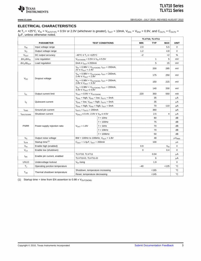
ELECTRICAL CHARACTERISTICSAt TJ = +25°C, VIN = VOUT(TYP) + 0.5V or 2.0V (whichever is greater), IOUT = 10mA, VEN1 = VEN2 = 0.9V, and COUT1 = COUT2 =1mF, unless otherwise noted.
TLV710, TLV711
PARAMETER TEST CONDITIONS MIN TYP MAX UNIT
VIN Input voltage range 2.0 5.5 V
VO Output voltage range 1.2 4.8 V
VOUT DC output accuracy –40°C ≤ TJ ≤ +125°C –2 +2 %
ΔVO/ΔVIN Line regulation VOUT(NOM) + 0.5V ≤ VIN ≤ 5.5V 1 5 mV
ΔVO/ΔIOUT Load regulation 0mA ≤ IOUT ≤ 200mA 5 15 mV
VIN = 0.98V × VOUT(NOM), IOUT = 200mA, 200 285 mV2V ≤ VOUT < 2.4V
VIN = 0.98V × VOUT(NOM), IOUT = 200mA, 175 250 mV2.4V ≤ VOUT < 2.8VVDO Dropout voltage
VIN = 0.98V × VOUT(NOM), IOUT = 200mA, 150 215 mV2.8V ≤ VOUT < 3.3V
VIN = 0.98V × VOUT(NOM), IOUT = 200mA, 140 200 mV3.3V ≤ VOUT ≤ 4.8V
ICL Output current limit VOUT = 0.9V × VOUT(NOM) 220 350 550 mA
VEN1 = high, VEN2 = low, IOUT1 = 0mA 35 mA
IQ Quiescent current VEN1 = low, VEN2 = high, IOUT2 = 0mA 35 mA
VEN1 = high, VEN2 = high, IOUT = 0mA 70 110 µA
IGND Ground pin current IOUT1 = IOUT2 = 200mA 360 µA
ISHUTDOWN Shutdown current VEN1,2 ≤ 0.4V, 2.0V ≤ VIN ≤ 4.5V 2.5 4 mA
f = 10Hz 80 dB
f = 100Hz 75 dB
PSRR Power-supply rejection ratio VOUT = 1.8V f = 1kHz 70 dB
f = 10kHz 70 dB
f = 100kHz 50 dB
VN Output noise voltage BW = 100Hz to 100kHz, VOUT = 1.8V 48 mVRMS
tSTR Startup time (1) COUT = 1.0mF, IOUT = 200mA 100 ms
VHI Enable high (enabled) 0.9 VIN V
VLO Enable low (shutdown) 0 0.4 V
TLV710, TLV711 0.04 mAIEN Enable pin current, enabled
TLV710-D, TLV711-D 6 mA
UVLO Undervoltage lockout VIN rising 1.9 V
TJ Operating junction temperature –40 +125 °C
Shutdown, temperature increasing +165 °CTSD Thermal shutdown temperature
Reset, temperature decreasing +145 °C
(1) Startup time = time from EN assertion to 0.98 x VOUT(NOM).
Copyright © 2010, Texas Instruments Incorporated Submit Documentation Feedback 3

T ermalh
Shutdown
UVLO
TLV710-D
and
TLV711-D
only
TLV711 and TLV711-D only
TLV710-D
and
TLV711-D
only
OUT1
OUT2
EN2
EN1
IN
120W
120W
150kW
Thermal
Shutdown
UVLO
GND
Current
Limit
Current
Limit
Bandgap
Bandgap
Enable
and
Power
Control
Log ci
TLV711 and TLV711-D only
TLV710 SeriesTLV711 Series
SBVS142A –JULY 2010–REVISED AUGUST 2010 www.ti.com
FUNCTIONAL BLOCK DIAGRAM
4 Submit Documentation Feedback Copyright © 2010, Texas Instruments Incorporated

OUT1
OUT2
GND
6
5
4
EN1
IN
EN2
1
2
3
TLV710 SeriesTLV711 Series
www.ti.com SBVS142A –JULY 2010–REVISED AUGUST 2010
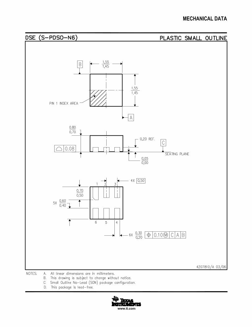
PIN CONFIGURATION
DSE PACKAGE1.5mm x 1.5mm SON-6
(TOP VIEW)
PIN DESCRIPTIONSNAME PIN NO. DESCRIPTION
Enable pin for regulator 1. Driving EN1 over 0.9V turns on regulator 1. Driving EN below 0.4V puts regulatorEN1 1 1 into shutdown mode.
Input pin. A small capacitor is needed from this pin to ground to assure stability. See Input and OutputIN 2 Capacitor Requirements in the Application Information section for more details.
Enable pin for regulator 2. Driving EN2 over 0.9V turns on regulator 2. Driving EN2 below 0.4V putsEN2 3 regulator2 into shutdown mode.
GND 4 Ground pin.
Regulated output voltage pin. A small 1mF ceramic capacitor is needed from this pin to ground to assureOUT2 5 stability. See Input and Output Capacitor Requirements in the Application Information section for more
details.
Regulated output voltage pin. A small 1mF ceramic capacitor is needed from this pin to ground to assureOUT1 6 stability. See Input and Output Capacitor Requirements in the Application Information section for more
details.
Copyright © 2010, Texas Instruments Incorporated Submit Documentation Feedback 5

1.90
1.88
1.86
1.84
1.82
1.80
1.78
1.76
1.74
1.72
1.70
V(V
)O
UT
2.1 2.6 3.1 3.6 4.1 4.6 5.1
V (V)IN
5.6
+125 C°
+85 C°
+25 C°
-40 C°
I = 10mAOUT1
I = 10mAOUT2
2.90
2.88
2.86
2.84
2.82
2.80
2.78
2.76
2.74
2.72
2.70
V(V
)O
UT
3.1 3.6 4.1 4.6 5.1 5.6
V (V)IN
+125 C°
+85 C°
+25 C°
-40 C°
I = 10mAOUT1
I = 10mAOUT2
1.90
1.88
1.86
1.84
1.82
1.80
1.78
1.76
1.74
1.72
1.70
V(V
)O
UT
2.1 2.6 3.1 3.6 4.1 4.6 5.1
V (V)IN
5.6
+125 C°
+85 C°
+25 C°
-40 C°
I = 200mAOUT1
I = 0mAOUT2
2.90
2.88
2.86
2.84
2.82
2.80
2.78
2.76
2.74
2.72
2.70
V(V
)O
UT
3.1 3.6 4.1 4.6 5.1 5.6
V (V)IN
+125 C°
+85 C°
+25 C°
-40 C°
I = 0mAOUT1
I = 200mAOUT2
3.40
3.38
3.36
3.34
3.32
3.30
3.28
3.26
3.24
3.22
3.20
V(V
)O
UT
3.6 3.8 4.0 4.2 4.4 4.6 4.8 5.0 5.2 5.4
V (V)IN
5.6
+125 C°
+85 C°
+25 C°
- °40 C
I = 10mAOUT1
I = 10mAOUT2
3.40
3.38
3.36
3.34
3.32
3.30
3.28
3.26
3.24
3.22
3.20
V(V
)O
UT
3.6 3.8 4.0 4.2 4.4 4.6 4.8 5.0 5.2 5.4
V (V)IN
5.6
+125 C°
+85 C°
+25 C°
-40 C°
I = 10mAOUT1
I = 10mAOUT2
TLV710 SeriesTLV711 Series
SBVS142A –JULY 2010–REVISED AUGUST 2010 www.ti.com
TYPICAL CHARACTERISTICSOver operating temperature range of TJ = –40°C to +125°C, VEN1 = VEN2 = VIN, CIN = 1mF, COUT1 = 1mF, and COUT2 = 1mF, unless otherwisenoted. Typical values are at TJ = +25°C.
LINE REGULATION: VOUT1 LINE REGULATION: VOUT2(TLV7101828) (TLV7101828)
Figure 1. Figure 2.
LINE REGULATION: VOUT1 LINE REGULATION: VOUT2(TLV7101828) (TLV7101828)
Figure 3. Figure 4.
LINE REGULATION: VOUT1 LINE REGULATION: VOUT2(TLV7103333) (TLV7103333)
Figure 5. Figure 6.
6 Submit Documentation Feedback Copyright © 2010, Texas Instruments Incorporated

3.40
3.38
3.36
3.34
3.32
3.30
3.28
3.26
3.24
3.22
3.20
V(V
)O
UT
3.6 3.8 4.0 4.2 4.4 4.6 4.8 5.0 5.2 5.4
V (V)IN
5.6
+125 C°
+85 C°
+25 C°
-40 C°
I = 200mAOUT1
I = 0mAOUT2
3.40
3.38
3.36
3.34
3.32
3.30
3.28
3.26
3.24
3.22
3.20
V(V
)O
UT
3.6 3.8 4.0 4.2 4.4 4.6 4.8 5.0 5.2 5.4
V (V)IN
5.6
+125 C°
+85 C°
+25 C°
-40 C°
I = 0mAOUT1
I = mAOUT2
200
1.60
1.58
1.56
1.54
1.52
1.50
1.48
1.46
1.44
1.42
1.40
V(V
)O
UT
2.0 2.5 3.0 3.5 4.0 4.5 5.0
V (V)IN
5.5
+125 C°
+85 C°
+25 C°
- °40 C
I = 10mAOUT1
I = 10mAOUT2
2.60
2.58
2.56
2.54
2.52
2.50
2.48
2.46
2.44
2.42
2.40
V(V
)O
UT
3.0 3.5 4.0 4.5 5.0
V (V)IN
5.5
+125 C°
+85 C°
+25 C°
- °40 C
I = 10mAOUT1
I = 10mAOUT2
1.60
1.58
1.56
1.54
1.52
1.50
1.48
1.46
1.44
1.42
1.40
V(V
)O
UT
2.0 2.5 3.0 3.5 4.0 4.5 5.0
V (V)IN
5.5
+125 C°
+85 C°
+25 C°
-40°C
I = 200mAOUT1
I = 0mAOUT2
2.60
2.58
2.56
2.54
2.52
2.50
2.48
2.46
2.44
2.42
2.40
V(V
)O
UT
3.0 3.5 4.0 4.5 5.0
V (V)IN
5.5
+125 C°
+85 C°
+25 C°
-40 C°
I = 0mAOUT1
TLV710 SeriesTLV711 Series
www.ti.com SBVS142A –JULY 2010–REVISED AUGUST 2010
TYPICAL CHARACTERISTICS (continued)Over operating temperature range of TJ = –40°C to +125°C, VEN1 = VEN2 = VIN, CIN = 1mF, COUT1 = 1mF, and COUT2 = 1mF,unless otherwise noted. Typical values are at TJ = +25°C.
LINE REGULATION: VOUT1 LINE REGULATION: VOUT2(TLV7103333) (TLV7103333)
Figure 7. Figure 8.
LINE REGULATION: VOUT1 LINE REGULATION: VOUT2(TLV7111525) (TLV7111525)
Figure 9. Figure 10.
LINE REGULATION: VOUT1 LINE REGULATION: VOUT2(TLV7111525) (TLV7111525)
Figure 11. Figure 12.
Copyright © 2010, Texas Instruments Incorporated Submit Documentation Feedback 7

1.90
1.88
1.86
1.84
1.82
1.80
1.78
1.76
1.74
1.72
1.70
V(V
)O
UT
0 20 40 60 80 100 120 140 160 180
I (mA)OUT
200
+125 C°
+85 C°
+25 C°
-40 C°
V = 3.3VIN
2.90
2.88
2.86
2.84
2.82
2.80
2.78
2.76
2.74
2.72
2.70
V(V
)O
UT
0 20 40 60 80 100 120 140 160 180
I (mA)OUT
200
+125 C°
+85 C°
+25 C°
- °40 C
V = 3.3VIN
3.40
3.38
3.36
3.34
3.32
3.30
3.28
3.26
3.24
3.22
3.20
V(V
)O
UT
0 20 40 60 80 100 120 140 160 180
I (mA)OUT
200
+125 C°
+85 C°
+25 C°
-40 C°
V = 3.8VIN
3.40
3.38
3.36
3.34
3.32
3.30
3.28
3.26
3.24
3.22
3.20
V(V
)O
UT
0 20 40 60 80 100 120 140 160 180
I (mA)OUT
200
+125 C°
+85 C°
+25 C°
-40°C
V = 3.8VIN
1.60
1.58
1.56
1.54
1.52
1.50
1.48
1.46
1.44
1.42
1.40
V(V
)O
UT
0 20 40 60 80 100 120 140 160 180
I (mA)OUT
200
+125 C°
+85 C°
+25 C°
-40°C
V = 3.0VIN
2.60
2.58
2.56
2.54
2.52
2.50
2.48
2.46
2.44
2.42
2.40
V(V
)O
UT
0 20 40 60 80 100 120 140 160 180
I (mA)OUT
200
+125 C°
+85 C°
+25 C°
-40°C
V = 3.0VIN
TLV710 SeriesTLV711 Series
SBVS142A –JULY 2010–REVISED AUGUST 2010 www.ti.com
TYPICAL CHARACTERISTICS (continued)Over operating temperature range of TJ = –40°C to +125°C, VEN1 = VEN2 = VIN, CIN = 1mF, COUT1 = 1mF, and COUT2 = 1mF,unless otherwise noted. Typical values are at TJ = +25°C.
LOAD REGULATION: VOUT1 LOAD REGULATION: VOUT2(TLV7101828) (TLV7101828)
Figure 13. Figure 14.
LOAD REGULATION: VOUT1 LOAD REGULATION: VOUT2(TLV7103333) (TLV7103333)
Figure 15. Figure 16.
LOAD REGULATION: VOUT1 LOAD REGULATION: VOUT2(TLV7111525) (TLV7111525)
Figure 17. Figure 18.
8 Submit Documentation Feedback Copyright © 2010, Texas Instruments Incorporated

70
60
50
40
30
20
10
0
V(m
V)
DO
2.0 2.4 2.8 3.2 3.6 4.0 4.4
V (V)IN
4.8
+125 C°
+85 C°
+25 C°
- °40 C
V = V = 4.8V
I = 50mA
OUT1 OUT2
OUT
120
100
80
60
40
20
0
V(m
V)
DO
2.0 2.4 2.8 3.2 3.6 4.0 4.4
V (V)IN
4.8
+125 C°
+85 C°
+25 C°
- °40 C
V = V = 4.8V
I = 100mA
OUT1 OUT2
OUT
180
160
140
120
100
80
60
40
20
0
V(m
V)
DO
2.0 2.4 2.8 3.2 3.6 4.0 4.4
V (V)IN
4.8
+125 C°
+85 C°
+25 C°
- °40 C
V = V = 4.8V
I = 150mA
OUT1 OUT2
OUT
250
200
150
100
50
0
V(m
V)
DO
2.0 2.4 2.8 3.2 3.6 4.0 4.4
V (V)IN
4.8
+125 C°
+85 C°
+25 C°
-40 C°
V = V = 4.8V
I = 200mA
OUT1 OUT2
OUT
200
180
160
140
120
100
80
60
40
20
0
V(m
V)
DO
0 20 40 60 80 100 120 140 160 180
I (mA)OUT
200
+125 C°
+85 C°
+25 C°
-40°C
180
160
140
120
100
80
60
40
20
0
V(m
V)
DO
0 20 40 60 80 100 120 140 160 180
I (mA)OUT
200
+125 C°
+85 C°
+25 C°
- °C40
TLV710 SeriesTLV711 Series
www.ti.com SBVS142A –JULY 2010–REVISED AUGUST 2010
TYPICAL CHARACTERISTICS (continued)Over operating temperature range of TJ = –40°C to +125°C, VEN1 = VEN2 = VIN, CIN = 1mF, COUT1 = 1mF, and COUT2 = 1mF,unless otherwise noted. Typical values are at TJ = +25°C.
DROPOUT VOLTAGE DROPOUT VOLTAGEvs INPUT VOLTAGE vs INPUT VOLTAGE
Figure 19. Figure 20.
DROPOUT VOLTAGE DROPOUT VOLTAGEvs INPUT VOLTAGE vs INPUT VOLTAGE
Figure 21. Figure 22.
DROPOUT VOLTAGE vs OUTPUT CURRENT: VOUT2 DROPOUT VOLTAGE vs OUTPUT CURRENT: VOUT1/VOUT2(TLV7101828) (TLV7103333)
Figure 23. Figure 24.
Copyright © 2010, Texas Instruments Incorporated Submit Documentation Feedback 9

250
200
150
100
50
0
V(m
V)
DO
0 20 40 60 80 100 120 140 160 180
I (mA)OUT
200
+125 C°
+85 C°
+25 C°
-40°C
1.90
1.88
1.86
1.84
1.82
1.80
1.78
1.76
1.74
1.72
1.70
V(V
)O
UT
-40 -25 -10 5 20 35 50 65 80 95 110
Junction Temperature ( C)°
125
10mA
150mA
200mA
V = 3.3VIN
2.90
2.88
2.86
2.84
2.82
2.80
2.78
2.76
2.74
2.72
2.70
V(V
)O
UT
-40 -25 -10 5 20 35 50 65 80 95 110
Junction Temperature ( C)°
125
10mA
150mA
200mA
V = 3.3VIN
3.40
3.38
3.36
3.34
3.32
3.30
3.28
3.26
3.24
3.22
3.20
V(V
)O
UT
-40 -25 -10 5 20 35 50 65 80 95 110
Junction Temperature ( C)°
125
10mA
150mA
200mA
V = 3.8VIN
3.40
3.38
3.36
3.34
3.32
3.30
3.28
3.26
3.24
3.22
3.20
V(V
)O
UT
-40 -25 -10 5 20 35 50 65 80 95 110
Junction Temperature ( C)°
125
10mA
150mA
200mA
V = 3.8VIN
1.60
1.58
1.56
1.54
1.52
1.50
1.48
1.46
1.44
1.42
1.40
V(V
)O
UT
-40 -25 -10 5 20 35 50 65 80 95 110
Junction Temperature ( C)°
125
10mA
150mA
200mA
V = 3.0VIN
TLV710 SeriesTLV711 Series
SBVS142A –JULY 2010–REVISED AUGUST 2010 www.ti.com
TYPICAL CHARACTERISTICS (continued)Over operating temperature range of TJ = –40°C to +125°C, VEN1 = VEN2 = VIN, CIN = 1mF, COUT1 = 1mF, and COUT2 = 1mF,unless otherwise noted. Typical values are at TJ = +25°C.
DROPOUT VOLTAGE vs OUTPUT CURRENT: VOUT2 OUTPUT VOLTAGE vs TEMPERATURE: VOUT1(TLV7111525) (TLV7101828)
Figure 25. Figure 26.
OUTPUT VOLTAGE vs TEMPERATURE: VOUT2 OUTPUT VOLTAGE vs TEMPERATURE: VOUT1(TLV7101828) (TLV7103333)
Figure 27. Figure 28.
OUTPUT VOLTAGE vs TEMPERATURE: VOUT2 OUTPUT VOLTAGE vs TEMPERATURE: VOUT1(TLV7103333) (TLV7111525)
Figure 29. Figure 30.
10 Submit Documentation Feedback Copyright © 2010, Texas Instruments Incorporated

2.60
2.58
2.56
2.54
2.52
2.50
2.48
2.46
2.44
2.42
2.40
V(V
)O
UT
-40 -25 -10 5 20 35 50 65 80 95 110
Junction Temperature ( C)°
125
10mA
150mA
200mA
V = 3.0VIN
50
45
40
35
30
25
20
15
10
5
0
I(m
A)
GN
D
2.1 2.6 3.1 3.6 4.1 4.6 5.1
V (V)IN
5.6
+125 C°
+85 C°
+25 C°
-40 C°
V = 3.3VIN
50
45
40
35
30
25
20
15
10
5
0
I(m
A)
GN
D
3.1 3.6 4.1 4.6 5.1
V (V)IN
5.6
+125 C°
+85 C°
+25 C°
- °40 C
50
45
40
35
30
25
20
15
10
5
0
I(m
A)
GN
D
3.6 4.0 4.4 4.8 5.2
V (V)IN
5.6
+125 C°
+85 C°
+25 C°
- °40 C
50
45
40
35
30
25
20
15
10
5
0
I(
A)
mG
ND
3.6 4.0 4.4 4.8 5.2
V (V)IN
5.6
+125 C°
+85 C°
+25 C°
- °40 C
50
45
40
35
30
25
20
15
10
5
0
I(
A)
mG
ND
2.1 2.6 3.1 3.6 4.1 4.6 5.1
V (V)IN
5.6
+125 C°
+85 C°
+25 C°
-40 C°
TLV710 SeriesTLV711 Series
www.ti.com SBVS142A –JULY 2010–REVISED AUGUST 2010
TYPICAL CHARACTERISTICS (continued)Over operating temperature range of TJ = –40°C to +125°C, VEN1 = VEN2 = VIN, CIN = 1mF, COUT1 = 1mF, and COUT2 = 1mF,unless otherwise noted. Typical values are at TJ = +25°C.
OUTPUT VOLTAGE vs TEMPERATURE: VOUT2 GROUND PIN CURRENT vs INPUT VOLTAGE: IQ1(TLV7111525) (TLV7101828)
Figure 31. Figure 32.
GROUND PIN CURRENT vs INPUT VOLTAGE: IQ2 GROUND PIN CURRENT vs INPUT VOLTAGE: IQ1(TLV7101828) (TLV7103333)
Figure 33. Figure 34.
GROUND PIN CURRENT vs INPUT VOLTAGE: IQ2 GROUND PIN CURRENT vs INPUT VOLTAGE: IQ1(TLV7103333) (TLV7111525)
Figure 35. Figure 36.
Copyright © 2010, Texas Instruments Incorporated Submit Documentation Feedback 11

50
45
40
35
30
25
20
15
10
5
0
I(m
A)
GN
D
2.8 3.2 3.6 4.0 4.4 4.8 5.2
V (V)IN
5.6
+125 C°
+85 C°
+25 C°
- °40 C
350
300
250
200
150
100
50
0
I(m
A)
GN
D
0 20 40 60 80 100 120 140 160 180 200
+125 C°
+85 C°
+25 C°
-40°C
V = 3.3VIN
I (mA)OUT
350
300
250
200
150
100
50
0
I(
A)
mG
ND
0 20 40 60 80 100 120 140 160 180
I (mA)OUT
200
+125 C°
+85 C°
+25 C°
-40 C°
V = 3.8VIN
350
300
250
200
150
100
50
0
I(m
A)
GN
D
0 20 40 60 80 100 120 140 160 180
I (mA)OUT
200
+125 C°
+85 C°
+25 C°
-40 C°
V = 3.0VIN
4.0
3.5
3.0
2.5
2.0
1.5
1.0
5
0
I(
A)
mS
HD
N
2.0 2.5 3.0 3.5 4.0 4.5 5.0
V (V)IN
5.5
+125 C°
+85 C°
+25 C°
- °40 C
4.0
3.5
3.0
2.5
2.0
1.5
1.0
5
0
I(
A)
mS
HD
N
2.0 2.5 3.0 3.5 4.0 4.5 5.0
V (V)IN
5.5
+125 C°
+85 C°
+25 C°
- °40 C
TLV710 SeriesTLV711 Series
SBVS142A –JULY 2010–REVISED AUGUST 2010 www.ti.com
TYPICAL CHARACTERISTICS (continued)Over operating temperature range of TJ = –40°C to +125°C, VEN1 = VEN2 = VIN, CIN = 1mF, COUT1 = 1mF, and COUT2 = 1mF,unless otherwise noted. Typical values are at TJ = +25°C.
GROUND PIN CURRENT vs INPUT VOLTAGE: IQ2 GROUND PIN CURRENT vs LOAD: IQ1(TLV7111525) (TLV7101828)
Figure 37. Figure 38.
GROUND PIN CURRENT vs LOAD: IQ2 GROUND PIN CURRENT vs LOAD: IQ1(TLV7103333) (TLV7111525)
Figure 39. Figure 40.
SHUTDOWN CURRENT vs INPUT VOLTAGE SHUTDOWN CURRENT vs INPUT VOLTAGE(TLV7101828) (TLV7103333)
Figure 41. Figure 42.
12 Submit Documentation Feedback Copyright © 2010, Texas Instruments Incorporated
4.0
3.5
3.0
2.5
2.0
1.5
1.0
5
0
I(
A)
mS
HD
N
2.0 2.5 3.0 3.5 4.0 4.5 5.0
V (V)IN
5.5
+125 C°
+85 C°
+25 C°
- °40 C
500
480
460
440
420
400
380
360
340
320
300
I(m
A)
LIM
2.1 2.6 3.1 3.6 4.1 4.6 5.1
V (V)IN
5.6
+125 C°
+85 C°
+25 C°
-40 C°
500
480
460
440
420
400
380
360
340
320
300
I(m
A)
LIM
3.1 3.6 4.1 4.6 5.1
V (V)IN
5.6
+125 C°
+85 C°
+25 C°
-40 C°
500
480
460
440
420
400
380
360
340
320
300
I(m
A)
LIM
3.6 4.0 4.4 4.8 5.2
V (V)IN
5.6
+125 C°
+85 C°
+25 C°
- °40 C
500
480
460
440
420
400
380
360
340
320
300
I(m
A)
LIM
3.6 4.0 4.4 4.8 5.2
V (V)IN
5.6
+125 C°
+85 C°
+25 C°
- °40 C
500
480
460
440
420
400
380
360
340
320
300
I(m
A)
LIM
2.8
V (V)IN
5.5
+125 C°
+85 C°
+25 C°
- °40 C
3.1 3.4 3.7 4.0 4.3 4.6 4.9 5.2
TLV710 SeriesTLV711 Series
www.ti.com SBVS142A –JULY 2010–REVISED AUGUST 2010
TYPICAL CHARACTERISTICS (continued)Over operating temperature range of TJ = –40°C to +125°C, VEN1 = VEN2 = VIN, CIN = 1mF, COUT1 = 1mF, and COUT2 = 1mF,unless otherwise noted. Typical values are at TJ = +25°C.
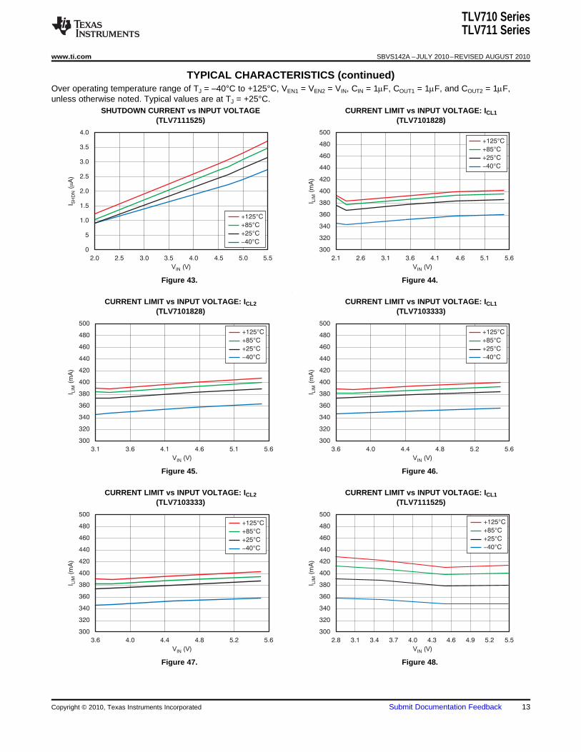
SHUTDOWN CURRENT vs INPUT VOLTAGE CURRENT LIMIT vs INPUT VOLTAGE: ICL1(TLV7111525) (TLV7101828)
Figure 43. Figure 44.
CURRENT LIMIT vs INPUT VOLTAGE: ICL2 CURRENT LIMIT vs INPUT VOLTAGE: ICL1(TLV7101828) (TLV7103333)
Figure 45. Figure 46.
CURRENT LIMIT vs INPUT VOLTAGE: ICL2 CURRENT LIMIT vs INPUT VOLTAGE: ICL1(TLV7103333) (TLV7111525)
Figure 47. Figure 48.
Copyright © 2010, Texas Instruments Incorporated Submit Documentation Feedback 13

500
480
460
440
420
400
380
360
340
320
300
I(m
A)
LIM
2.8
V (V)IN
5.5
+125 C°
+85 C°
+25 C°
- °40 C
3.1 3.4 3.7 4.0 4.3 4.6 4.9 5.2
100
90
80
70
60
50
40
30
20
10
0
PS
RR
(dB
)
10 100 1k 10k
Frequency (Hz)
100k 1M 10M
I = 30mAOUT2
I = 30mAOUT1
V = 3.3VIN
V = 2.8VOUT
I = 150mAOUT2
100
80
70
60
50
40
30
20
10
0
PS
RR
(dB
)
10 100 1k 10k
Frequency (Hz)
100k 1M 10M
I = 30mAOUT2 I = 30mA
OUT1
V = 3.8VIN
V = 3.3VOUT
I = 150mAOUT2
90
100
90
80
70
60
50
40
30
20
10
0
PS
RR
(dB
)
10 100 1k 10k
Frequency (Hz)
100k 1M 10M
I = 30mAOUT2
I = 30mAOUT1
V = 3.0VIN
V = 2.5VOUT
I = 150 AmOUT2
10
1
0.1
0.01
0.001
Outp
ut S
pectr
al N
ois
e D
ensity (
mV
/ÖH
z)
10 100 1k 10k
Frequency (Hz)
100k 1M 10M
V = 3.3VIN
V = 2.8VOUT2
I = 30mAOUT2
TLV710 SeriesTLV711 Series
SBVS142A –JULY 2010–REVISED AUGUST 2010 www.ti.com
TYPICAL CHARACTERISTICS (continued)Over operating temperature range of TJ = –40°C to +125°C, VEN1 = VEN2 = VIN, CIN = 1mF, COUT1 = 1mF, and COUT2 = 1mF,unless otherwise noted. Typical values are at TJ = +25°C.
CURRENT LIMIT vs INPUT VOLTAGE: ICL2(TLV7111525)
Figure 49.
POWER-SUPPLY RIPPLE REJECTION vs FREQUENCY POWER-SUPPLY RIPPLE REJECTION vs FREQUENCY(TLV7101828) (TLV7103333)
Figure 50. Figure 51.
POWER-SUPPLY RIPPLE REJECTION vs FREQUENCY OUTPUT SPECTRAL NOISE DENSITY(TLV7111525) vs FREQUENCY (TLV7101828)
Figure 52. Figure 53.
14 Submit Documentation Feedback Copyright © 2010, Texas Instruments Incorporated

10
1
0.1
0.01
0.001
Outp
ut S
pectr
al N
ois
e D
ensity (
mÖ
V/
)H
z
10 100 1k 10k
Frequency (Hz)
100k 1M 10M
V = 3.8VIN
V = 3.3VOUT2
I = 30mAOUT2
10
1
0.1
0.01
0.001
Outp
ut S
pectr
al N
ois
e D
ensity (
mV
/ÖH
z)
10 100 1k 10k
Frequency (Hz)
100k 1M 10M
V = 3.0VIN
V = 1.5VOUT1
I = 30mAOUT1
3.0V
2.0V
Time (200 s/div)m
VIN
1V/div
5mV/div
5mV/div
VOUT1
VOUT2
Slew Rate = 1V/ s
I = 30mA
m
OUT
5.5V
Time (200 s/div)m
VIN2V/div
5mV/div
5mV/div
VOUT1
VOUT2
2.0V
Slew Rate = 1V/ s
I = 30mA
m
OUT
4.3V
3.3V
Time (200 s/div)m
VIN
1V/div
5mV/div
5mV/div
VOUT1
VOUT2
Slew Rate = 1V/ s
I = 30mA
m
OUT
5.5V
Time (200 s/div)m
VIN1V/div
5mV/div
5mV/div
VOUT1
VOUT2
3.3V
Slew Rate = 1V/ s
I = 30mA
m
OUT
TLV710 SeriesTLV711 Series
www.ti.com SBVS142A –JULY 2010–REVISED AUGUST 2010
TYPICAL CHARACTERISTICS (continued)Over operating temperature range of TJ = –40°C to +125°C, VEN1 = VEN2 = VIN, CIN = 1mF, COUT1 = 1mF, and COUT2 = 1mF,unless otherwise noted. Typical values are at TJ = +25°C.
OUTPUT SPECTRAL NOISE DENSITY OUTPUT SPECTRAL NOISE DENSITYvs FREQUENCY (TLV7103333) vs FREQUENCY (TLV7111525)
Figure 54. Figure 55.
LINE TRANSIENT RESPONSE LINE TRANSIENT RESPONSEVOUT1 = 1.2V, VOUT2 = 1.2V VOUT1 = 1.2V, VOUT2 = 1.2V
Figure 56. Figure 57.
LINE TRANSIENT RESPONSE LINE TRANSIENT RESPONSEVOUT1 = 1.8V, VOUT2 = 2.8V VOUT1 = 1.8V, VOUT2 = 2.8V
Figure 58. Figure 59.
Copyright © 2010, Texas Instruments Incorporated Submit Documentation Feedback 15

5.5V
5.3V
Time (200 s/div)m
VIN
1V/div
5mV/div
5mV/div
VOUT1
VOUT2
Slew Rate = 1V/ s
I = 30mA
m
OUT
0mA
Time (50 s/div)m
IOUT1
VOUT1
VOUT2
200mA
100mA/div
50mV/div
10mV/div
Slew Rate = 1V/ s
V = 2.0V
m
IN
Time (50 s/div)m
IOUT1
VOUT1
VOUT2
200mA
100mA/div
50mV/div
10mV/div
Slew Rate = 1V/ s
V = 2.0V
m
IN
50mA
0mA
Time (50 s/div)m
IOUT2
VOUT1
VOUT2
200mA
100mA/div
50mV/div
50mV/div
Slew Rate = 1V/ s
V = 3.3V
m
IN
50mA
Time (50 s/div)m
IOUT2
VOUT2
VOUT1
200mA
100mA/div
20mV/div
5mV/div
Slew Rate = 1V/ s
V = 3.3V
m
IN
TLV710 SeriesTLV711 Series
SBVS142A –JULY 2010–REVISED AUGUST 2010 www.ti.com
TYPICAL CHARACTERISTICS (continued)Over operating temperature range of TJ = –40°C to +125°C, VEN1 = VEN2 = VIN, CIN = 1mF, COUT1 = 1mF, and COUT2 = 1mF,unless otherwise noted. Typical values are at TJ = +25°C.
LINE TRANSIENT RESPONSEVOUT1 = 4.8V, VOUT2 = 4.8V
Figure 60.
LOAD TRANSIENT RESPONSE AND CROSSTALK LOAD TRANSIENT RESPONSE AND CROSSTALKVOUT1 = 1.2V, VOUT2 = 1.2V VOUT1 = 1.2V, VOUT2 = 1.2V
Figure 61. Figure 62.
LOAD TRANSIENT RESPONSE AND CROSSTALK LOAD TRANSIENT RESPONSE AND CROSSTALKVOUT1 = 1.8V, VOUT2 = 2.8V VOUT1 = 1.8V, VOUT2 = 2.8V
Figure 63. Figure 64.
16 Submit Documentation Feedback Copyright © 2010, Texas Instruments Incorporated

0mA
Time (50 s/div)m
IOUT1
VOUT1
VOUT2
200mA
100mA/div
50mV/div
5mV/div
Slew Rate = 1V/ s
V = 5.3V
m
IN
50mA
Time (50 s/div)m
IOUT1
VOUT1
VOUT2
200mA
50mA/div
50mV/div
5mV/div
Slew Rate = 1V/ s
V = 5.3V
m
IN
Time (200ms/div)
1V/div
V /VOUT1 OUT2
I = 30mAOUT
V VIN/ EN
Time (200ms/div)
1V/div VOUT2
VOUT1
V VIN/ EN
I = 30mAOUT
Time (200ms/div)
1V/div V /VOUT1 OUT2
V VIN/ EN
I = 30mAOUT
TLV710 SeriesTLV711 Series
www.ti.com SBVS142A –JULY 2010–REVISED AUGUST 2010
TYPICAL CHARACTERISTICS (continued)Over operating temperature range of TJ = –40°C to +125°C, VEN1 = VEN2 = VIN, CIN = 1mF, COUT1 = 1mF, and COUT2 = 1mF,unless otherwise noted. Typical values are at TJ = +25°C.
LOAD TRANSIENT RESPONSE AND CROSSTALK LOAD TRANSIENT RESPONSE AND CROSSTALKVOUT1 = 4.8V, VOUT2 = 4.8V VOUT1 = 4.8V, VOUT2 = 4.8V
Figure 65. Figure 66.
VIN RAMP UP, RAMP DOWN RESPONSE VIN RAMP UP, RAMP DOWN RESPONSEVOUT1 = 1.2V, VOUT2 = 1.2V VOUT1 = 1.8V, VOUT2 = 2.8V
Figure 67. Figure 68.
VIN RAMP UP, RAMP DOWN RESPONSEVOUT1 = 4.8V, VOUT2 = 4.8V
Figure 69.
Copyright © 2010, Texas Instruments Incorporated Submit Documentation Feedback 17

t =120 · R
L
120 + RL
· COUT
TLV710 SeriesTLV711 Series
SBVS142A –JULY 2010–REVISED AUGUST 2010 www.ti.com
APPLICATION INFORMATION
The TLV710 and TLV711 series of devices belong to BOARD LAYOUT RECOMMENDATIONS TOa new family of next generation, value LDO IMPROVE PSRR AND NOISE PERFORMANCEregulators. These devices consume low quiescentcurrent and deliver excellent line and load transient Input and output capacitors should be placed asperformance. These features, combined with low close to the device pins as possible. To improve acnoise, very good PSRR with little (VIN to VOUT) performance such as PSRR, output noise, andheadroom, make these devices ideal for RF portable transient response, it is recommended that the boardapplications. This family of LDO regulators offers be designed with separate ground planes for VIN andcurrent limit and thermal protection, and is specified VOUT, with the ground plane connected only at thefrom –40°C to +125°C. GND pin of the device. In addition, the ground
connection for the output capacitor should beINPUT AND OUTPUT CAPACITOR connected directly to the GND pin of the device. HighREQUIREMENTS ESR capacitors may degrade PSRR.
1.0mF X5R- and X7R-type ceramic capacitors are INTERNAL CURRENT LIMITrecommended because they have minimal variationin value and equivalent series resistance (ESR) over The TLV710 and TLV711 internal current limits helptemperature. protect the regulator during fault conditions. During
current limit, the output sources a fixed amount ofHowever, the TLV710 and TLV711 are designed tocurrent that is largely independent of output voltage.be stable with an effective capacitance of 0.1mF orIn such a case, the output voltage is not regulated,larger at the output. Thus, the device would also beand is VOUT = ILIMIT × RLOAD.stable with capacitors of other dielectrics, as long as
the effective capacitance under operating bias The PMOS pass transistor dissipates (VIN – VOUT) ×voltage and temperature is greater than 0.1mF. This ILIMIT until thermal shutdown is triggered and theeffective capacitance refers to the capacitance that device is turned off. As the device cools down, it isthe device sees under operating bias voltage and turned on by the internal thermal shutdown circuit. Iftemperature conditions (that is, the capacitance after the fault condition continues, the device cyclestaking bias voltage and temperature derating into between current limit and thermal shutdown. See theconsideration.) Thermal Information section for more details. The
PMOS pass element in the TLV710 and TLV711 hasIn addition to allowing the use of cost-effectivea built-in body diode that conducts current when thedielectrics, these devices also enable using smallervoltage at OUT exceeds the voltage at IN. Thisfootprint capacitors that have a higher derating incurrent is not limited, so if extended reverse voltagesize-constrained applications.operation is anticipated, external limiting to 5% of
Note that using a 0.1mF rating capacitor at the output rated output current is recommended.of the LDO regulator does not ensure stabilitybecause the effective capacitance under operating SHUTDOWNconditions would be less than 0.1mF. The maximum
The enable pin (EN) is active high. The device isESR should be less than 200mΩ.enabled when EN pin goes above 0.9V. This
Although an input capacitor is not required for relatively lower value of voltage needed to turn thestability, it is good analog design practice to connect LDO regulator on can be used to enable the devicea 0.1mF to 1.0mF low ESR capacitor across the IN with the GPIO of recent processors whose GPIOand GND pins of the regulator. This capacitor voltage is lower than traditional microcontrollers.counteracts reactive input sources and improves
The device is turned off when the EN pin is held attransient response, noise rejection, and rippleless than 0.4V. When shutdown capability is notrejection. A higher-value capacitor may be necessaryrequired, the EN pin can connected to the IN pin.if large, fast-rise-time load transients are anticipated,
or if the device is not located near the power source. The TLV711 has internal pull-down circuitry thatIf source impedance is more than 2Ω, a 0.1mF input discharges output with a time constant of:capacitor may be necessary to ensure stability.
Where:RL = load resistanceCOUT = output capacitor (1)
18 Submit Documentation Feedback Copyright © 2010, Texas Instruments Incorporated

TLV710 SeriesTLV711 Series
www.ti.com SBVS142A –JULY 2010–REVISED AUGUST 2010
DROPOUT VOLTAGE use worst-case loads and signal conditions. For goodreliability, thermal protection should trigger at least
The TLV710 and TLV711 use a PMOS pass +35°C above the maximum expected ambienttransistor to achieve low dropout. When (VIN – VOUT) condition of the particular application. Thisis less than the dropout voltage (VDO), the PMOS configuration produces a worst-case junctionpass device is in the linear region of operation and temperature of +125°C at the highest expectedthe input-to-output resistance is the RDS(ON) of the ambient temperature and worst-case load.PMOS pass element. VDO scales approximately withthe output current because the PMOS device The internal protection circuitry of the TLV710 andbehaves as a resistor in dropout. TLV711 has been designed to protect against
overload conditions. It was not intended to replaceAs with any linear regulator, PSRR and transient proper heatsinking. Continuously running theresponse are degraded as (VIN – VOUT) approaches TLV710/ TLV711 into thermal shutdown degradesdropout. device reliability.
TRANSIENT RESPONSE POWER DISSIPATIONAs with any regulator, increasing the size of the The ability to remove heat from a die is different foroutput capacitor reduces over/undershoot magnitude each package type, presenting differentbut increases duration of the transient response. considerations in the printed circuit board (PCB)
layout. The PCB area around the device that is freeThe TLV710 and TLV711 each have a dedicatedof other components moves the heat from the deviceVREF. Consequently, crosstalk from one channel toto the ambient air.the other as a result of transients is close to 0V.
Performance data for the TLV710 evaluation moduleUNDERVOLTAGE LOCKOUT (UVLO) (EVM) are shown in Table 1. The EVM is a 2-layer
board with 2 ounces of copper per side. TheThe TLV710 and TLV711 use an undervoltagedimension and layout are shown in Figure 70 andlockout circuit to keep the output shut off until theFigure 71. Using heavier copper increases theinternal circuitry is operating properly.effectiveness of removing heat from the device. Theaddition of plated through-holes in theTHERMAL INFORMATIONheat-dissipating layer also improves the heatsink
Thermal protection disables the output when the effectiveness. Power dissipation depends on inputjunction temperature rises to approximately +165°C, voltage and load conditions.allowing the device to cool. When the junction
Power dissipation (PD) is equal to the product of thetemperature cools to approximately +145°C, theoutput current and the voltage drop across the outputoutput circuitry is again enabled. Depending on powerpass element, as shown in Equation 2:dissipation, thermal resistance, and ambient
PD = (VIN – VOUT) × IOUT (2)temperature, the thermal protection circuit may cycleon and off. This cycling limits the dissipation of theregulator, protecting it from damage as a result of PACKAGE MOUNTINGoverheating.
Solder pad footprint recommendations for the TLV710Any tendency to activate the thermal protection circuit and TLV711 are available from the Texas Instrumentsindicates excessive power dissipation or an Web site at www.ti.com. The recommended landinadequate heatsink. For reliable operation, junction pattern for the DSE (SON-6) package is shown intemperature should be limited to +125°C maximum. Figure 72.To estimate the margin of safety in a complete design(including heatsink), increase the ambienttemperature until the thermal protection is triggered;
Table 1. TLV710 EVM Dissipation Ratings
PACKAGE RqJA TA < +25°C TA = +70°C TA = +85°C
DSE 170°C/W 585mW 320mW 235mW
Copyright © 2010, Texas Instruments Incorporated Submit Documentation Feedback 19

33mm
27mm
33mm
27mm
TLV710 SeriesTLV711 Series
SBVS142A –JULY 2010–REVISED AUGUST 2010 www.ti.com
Figure 70. Top Layer
Figure 71. Bottom Layer
20 Submit Documentation Feedback Copyright © 2010, Texas Instruments Incorporated

TLV710 SeriesTLV711 Series
www.ti.com SBVS142A –JULY 2010–REVISED AUGUST 2010
Figure 72. Land Pattern Drawing for DSE (SON-6) Package
Copyright © 2010, Texas Instruments Incorporated Submit Documentation Feedback 21

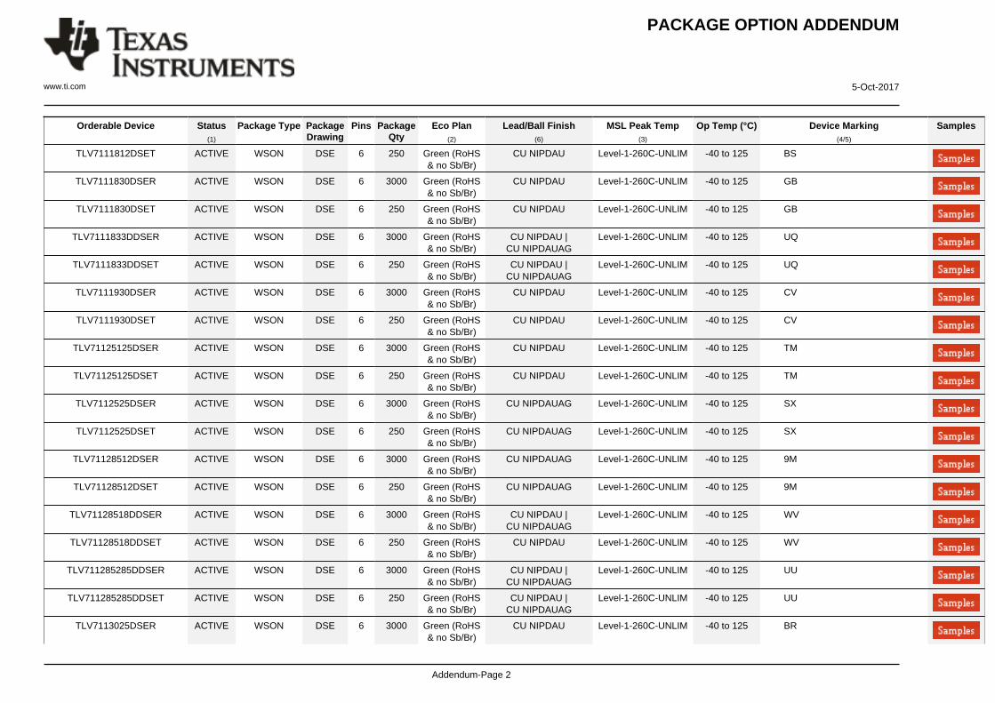
PACKAGE OPTION ADDENDUM
www.ti.com 5-Oct-2017
Addendum-Page 1
PACKAGING INFORMATION
Orderable Device Status(1)
Package Type PackageDrawing
Pins PackageQty
Eco Plan(2)
Lead/Ball Finish(6)
MSL Peak Temp(3)
Op Temp (°C) Device Marking(4/5)
Samples
TLV7101828DSER ACTIVE WSON DSE 6 3000 Green (RoHS& no Sb/Br)
CU NIPDAU Level-1-260C-UNLIM -40 to 125 QW
TLV7101828DSET ACTIVE WSON DSE 6 250 Green (RoHS& no Sb/Br)
CU NIPDAU Level-1-260C-UNLIM -40 to 125 QW
TLV7103318DSER ACTIVE WSON DSE 6 3000 Green (RoHS& no Sb/Br)
CU NIPDAUAG Level-1-260C-UNLIM -40 to 125 UE
TLV7103318DSET ACTIVE WSON DSE 6 250 Green (RoHS& no Sb/Br)
CU NIPDAUAG Level-1-260C-UNLIM -40 to 125 UE
TLV7111225DSER ACTIVE WSON DSE 6 3000 Green (RoHS& no Sb/Br)
CU NIPDAU Level-1-260C-UNLIM -40 to 125 BT
TLV7111225DSET ACTIVE WSON DSE 6 250 Green (RoHS& no Sb/Br)
CU NIPDAU Level-1-260C-UNLIM -40 to 125 BT
TLV7111233DSER ACTIVE WSON DSE 6 3000 Green (RoHS& no Sb/Br)
CU NIPDAU Level-1-260C-UNLIM -40 to 125 TP
TLV7111233DSET ACTIVE WSON DSE 6 250 Green (RoHS& no Sb/Br)
CU NIPDAU Level-1-260C-UNLIM -40 to 125 TP
TLV7111323DDSER ACTIVE WSON DSE 6 3000 Green (RoHS& no Sb/Br)
CU NIPDAUAG Level-1-260C-UNLIM -40 to 125 WH
TLV7111323DDSET ACTIVE WSON DSE 6 250 Green (RoHS& no Sb/Br)
CU NIPDAU Level-1-260C-UNLIM -40 to 125 WH
TLV7111333DDSER ACTIVE WSON DSE 6 3000 Green (RoHS& no Sb/Br)
CU NIPDAU Level-1-260C-UNLIM -40 to 125 YY
TLV7111333DDSET ACTIVE WSON DSE 6 250 Green (RoHS& no Sb/Br)
CU NIPDAU Level-1-260C-UNLIM -40 to 125 YY
TLV7111518DDSER ACTIVE WSON DSE 6 3000 Green (RoHS& no Sb/Br)
CU NIPDAU |CU NIPDAUAG
Level-1-260C-UNLIM -40 to 125 UT
TLV7111518DDSET ACTIVE WSON DSE 6 250 Green (RoHS& no Sb/Br)
CU NIPDAU |CU NIPDAUAG
Level-1-260C-UNLIM -40 to 125 UT
TLV7111533DDSER ACTIVE WSON DSE 6 3000 Green (RoHS& no Sb/Br)
CU NIPDAU Level-1-260C-UNLIM -40 to 125 YD
TLV7111533DDSET ACTIVE WSON DSE 6 250 Green (RoHS& no Sb/Br)
CU NIPDAU Level-1-260C-UNLIM -40 to 125 YD
TLV7111812DSER ACTIVE WSON DSE 6 3000 Green (RoHS& no Sb/Br)
CU NIPDAU Level-1-260C-UNLIM -40 to 125 BS
PACKAGE OPTION ADDENDUM
www.ti.com 5-Oct-2017
Addendum-Page 2
Orderable Device Status(1)
Package Type PackageDrawing
Pins PackageQty
Eco Plan(2)
Lead/Ball Finish(6)
MSL Peak Temp(3)
Op Temp (°C) Device Marking(4/5)
Samples
TLV7111812DSET ACTIVE WSON DSE 6 250 Green (RoHS& no Sb/Br)
CU NIPDAU Level-1-260C-UNLIM -40 to 125 BS
TLV7111830DSER ACTIVE WSON DSE 6 3000 Green (RoHS& no Sb/Br)
CU NIPDAU Level-1-260C-UNLIM -40 to 125 GB
TLV7111830DSET ACTIVE WSON DSE 6 250 Green (RoHS& no Sb/Br)
CU NIPDAU Level-1-260C-UNLIM -40 to 125 GB
TLV7111833DDSER ACTIVE WSON DSE 6 3000 Green (RoHS& no Sb/Br)
CU NIPDAU |CU NIPDAUAG
Level-1-260C-UNLIM -40 to 125 UQ
TLV7111833DDSET ACTIVE WSON DSE 6 250 Green (RoHS& no Sb/Br)
CU NIPDAU |CU NIPDAUAG
Level-1-260C-UNLIM -40 to 125 UQ
TLV7111930DSER ACTIVE WSON DSE 6 3000 Green (RoHS& no Sb/Br)
CU NIPDAU Level-1-260C-UNLIM -40 to 125 CV
TLV7111930DSET ACTIVE WSON DSE 6 250 Green (RoHS& no Sb/Br)
CU NIPDAU Level-1-260C-UNLIM -40 to 125 CV
TLV71125125DSER ACTIVE WSON DSE 6 3000 Green (RoHS& no Sb/Br)
CU NIPDAU Level-1-260C-UNLIM -40 to 125 TM
TLV71125125DSET ACTIVE WSON DSE 6 250 Green (RoHS& no Sb/Br)
CU NIPDAU Level-1-260C-UNLIM -40 to 125 TM
TLV7112525DSER ACTIVE WSON DSE 6 3000 Green (RoHS& no Sb/Br)
CU NIPDAUAG Level-1-260C-UNLIM -40 to 125 SX
TLV7112525DSET ACTIVE WSON DSE 6 250 Green (RoHS& no Sb/Br)
CU NIPDAUAG Level-1-260C-UNLIM -40 to 125 SX
TLV71128512DSER ACTIVE WSON DSE 6 3000 Green (RoHS& no Sb/Br)
CU NIPDAUAG Level-1-260C-UNLIM -40 to 125 9M
TLV71128512DSET ACTIVE WSON DSE 6 250 Green (RoHS& no Sb/Br)
CU NIPDAUAG Level-1-260C-UNLIM -40 to 125 9M
TLV71128518DDSER ACTIVE WSON DSE 6 3000 Green (RoHS& no Sb/Br)
CU NIPDAU |CU NIPDAUAG
Level-1-260C-UNLIM -40 to 125 WV
TLV71128518DDSET ACTIVE WSON DSE 6 250 Green (RoHS& no Sb/Br)
CU NIPDAU Level-1-260C-UNLIM -40 to 125 WV
TLV711285285DDSER ACTIVE WSON DSE 6 3000 Green (RoHS& no Sb/Br)
CU NIPDAU |CU NIPDAUAG
Level-1-260C-UNLIM -40 to 125 UU
TLV711285285DDSET ACTIVE WSON DSE 6 250 Green (RoHS& no Sb/Br)
CU NIPDAU |CU NIPDAUAG
Level-1-260C-UNLIM -40 to 125 UU
TLV7113025DSER ACTIVE WSON DSE 6 3000 Green (RoHS& no Sb/Br)
CU NIPDAU Level-1-260C-UNLIM -40 to 125 BR

PACKAGE OPTION ADDENDUM
www.ti.com 5-Oct-2017
Addendum-Page 3
Orderable Device Status(1)
Package Type PackageDrawing
Pins PackageQty
Eco Plan(2)
Lead/Ball Finish(6)
MSL Peak Temp(3)
Op Temp (°C) Device Marking(4/5)
Samples
TLV7113025DSET ACTIVE WSON DSE 6 250 Green (RoHS& no Sb/Br)
CU NIPDAU Level-1-260C-UNLIM -40 to 125 BR
TLV7113030DDSER ACTIVE WSON DSE 6 3000 Green (RoHS& no Sb/Br)
CU NIPDAUAG Level-1-260C-UNLIM -40 to 125 WS
TLV7113030DDSET ACTIVE WSON DSE 6 250 Green (RoHS& no Sb/Br)
CU NIPDAU Level-1-260C-UNLIM -40 to 125 WS
TLV7113318DDSER ACTIVE WSON DSE 6 3000 Green (RoHS& no Sb/Br)
CU NIPDAU |CU NIPDAUAG
Level-1-260C-UNLIM -40 to 125 VW
TLV7113318DDSET ACTIVE WSON DSE 6 250 Green (RoHS& no Sb/Br)
CU NIPDAU |CU NIPDAUAG
Level-1-260C-UNLIM -40 to 125 VW
TLV71133285DDSER ACTIVE WSON DSE 6 3000 Green (RoHS& no Sb/Br)
CU NIPDAU |CU NIPDAUAG
Level-1-260C-UNLIM -40 to 125 YE
TLV71133285DDSET ACTIVE WSON DSE 6 250 Green (RoHS& no Sb/Br)
CU NIPDAU Level-1-260C-UNLIM -40 to 125 YE
TLV7113330DDSER ACTIVE WSON DSE 6 3000 Green (RoHS& no Sb/Br)
CU NIPDAU |CU NIPDAUAG
Level-1-260C-UNLIM -40 to 125 WZ
TLV7113330DDSET ACTIVE WSON DSE 6 250 Green (RoHS& no Sb/Br)
CU NIPDAU Level-1-260C-UNLIM -40 to 125 WZ
TLV7113333DDSER ACTIVE WSON DSE 6 3000 Green (RoHS& no Sb/Br)
CU NIPDAU |CU NIPDAUAG
Level-1-260C-UNLIM -40 to 125 RV
TLV7113333DDSET ACTIVE WSON DSE 6 250 Green (RoHS& no Sb/Br)
CU NIPDAU |CU NIPDAUAG
Level-1-260C-UNLIM -40 to 125 RV
(1) The marketing status values are defined as follows:ACTIVE: Product device recommended for new designs.LIFEBUY: TI has announced that the device will be discontinued, and a lifetime-buy period is in effect.NRND: Not recommended for new designs. Device is in production to support existing customers, but TI does not recommend using this part in a new design.PREVIEW: Device has been announced but is not in production. Samples may or may not be available.OBSOLETE: TI has discontinued the production of the device.
(2) RoHS: TI defines "RoHS" to mean semiconductor products that are compliant with the current EU RoHS requirements for all 10 RoHS substances, including the requirement that RoHS substancedo not exceed 0.1% by weight in homogeneous materials. Where designed to be soldered at high temperatures, "RoHS" products are suitable for use in specified lead-free processes. TI mayreference these types of products as "Pb-Free".RoHS Exempt: TI defines "RoHS Exempt" to mean products that contain lead but are compliant with EU RoHS pursuant to a specific EU RoHS exemption.Green: TI defines "Green" to mean the content of Chlorine (Cl) and Bromine (Br) based flame retardants meet JS709B low halogen requirements of <=1000ppm threshold. Antimony trioxide basedflame retardants must also meet the <=1000ppm threshold requirement.
(3) MSL, Peak Temp. - The Moisture Sensitivity Level rating according to the JEDEC industry standard classifications, and peak solder temperature.

PACKAGE OPTION ADDENDUM
www.ti.com 5-Oct-2017
Addendum-Page 4
(4) There may be additional marking, which relates to the logo, the lot trace code information, or the environmental category on the device.
(5) Multiple Device Markings will be inside parentheses. Only one Device Marking contained in parentheses and separated by a "~" will appear on a device. If a line is indented then it is a continuationof the previous line and the two combined represent the entire Device Marking for that device.
(6) Lead/Ball Finish - Orderable Devices may have multiple material finish options. Finish options are separated by a vertical ruled line. Lead/Ball Finish values may wrap to two lines if the finishvalue exceeds the maximum column width.
Important Information and Disclaimer:The information provided on this page represents TI's knowledge and belief as of the date that it is provided. TI bases its knowledge and belief on informationprovided by third parties, and makes no representation or warranty as to the accuracy of such information. Efforts are underway to better integrate information from third parties. TI has taken andcontinues to take reasonable steps to provide representative and accurate information but may not have conducted destructive testing or chemical analysis on incoming materials and chemicals.TI and TI suppliers consider certain information to be proprietary, and thus CAS numbers and other limited information may not be available for release.
In no event shall TI's liability arising out of such information exceed the total purchase price of the TI part(s) at issue in this document sold by TI to Customer on an annual basis.
OTHER QUALIFIED VERSIONS OF TLV710 :
• Automotive: TLV710-Q1
NOTE: Qualified Version Definitions:
• Automotive - Q100 devices qualified for high-reliability automotive applications targeting zero defects

TAPE AND REEL INFORMATION
*All dimensions are nominal
Device PackageType
PackageDrawing
Pins SPQ ReelDiameter
(mm)
ReelWidth
W1 (mm)
A0(mm)
B0(mm)
K0(mm)
P1(mm)
W(mm)
Pin1Quadrant
TLV7101828DSER WSON DSE 6 3000 179.0 8.4 1.8 1.8 1.0 4.0 8.0 Q2
TLV7101828DSET WSON DSE 6 250 179.0 8.4 1.8 1.8 1.0 4.0 8.0 Q2
TLV7103318DSER WSON DSE 6 3000 179.0 8.4 1.8 1.8 1.0 4.0 8.0 Q2
TLV7103318DSET WSON DSE 6 250 179.0 8.4 1.8 1.8 1.0 4.0 8.0 Q2
TLV7111225DSER WSON DSE 6 3000 180.0 8.4 1.83 1.83 0.89 4.0 8.0 Q2
TLV7111225DSET WSON DSE 6 250 180.0 8.4 1.83 1.83 0.89 4.0 8.0 Q2
TLV7111233DSER WSON DSE 6 3000 180.0 8.4 1.83 1.83 0.89 4.0 8.0 Q2
TLV7111233DSET WSON DSE 6 250 180.0 8.4 1.83 1.83 0.89 4.0 8.0 Q2
TLV7111323DDSER WSON DSE 6 3000 179.0 8.4 1.8 1.8 1.0 4.0 8.0 Q2
TLV7111323DDSET WSON DSE 6 250 179.0 8.4 1.8 1.8 1.0 4.0 8.0 Q2
TLV7111333DDSER WSON DSE 6 3000 179.0 8.4 1.8 1.8 1.0 4.0 8.0 Q2
TLV7111333DDSET WSON DSE 6 250 179.0 8.4 1.8 1.8 1.0 4.0 8.0 Q2
TLV7111518DDSER WSON DSE 6 3000 179.0 8.4 1.8 1.8 1.0 4.0 8.0 Q2
TLV7111518DDSER WSON DSE 6 3000 178.0 8.4 1.7 1.7 0.95 4.0 8.0 Q2
TLV7111518DDSET WSON DSE 6 250 179.0 8.4 1.8 1.8 1.0 4.0 8.0 Q2
TLV7111518DDSET WSON DSE 6 250 178.0 8.4 1.7 1.7 0.95 4.0 8.0 Q2
TLV7111533DDSER WSON DSE 6 3000 179.0 8.4 1.8 1.8 1.0 4.0 8.0 Q2
TLV7111533DDSET WSON DSE 6 250 179.0 8.4 1.8 1.8 1.0 4.0 8.0 Q2
PACKAGE MATERIALS INFORMATION
www.ti.com 17-Feb-2018
Pack Materials-Page 1

Device PackageType
PackageDrawing
Pins SPQ ReelDiameter
(mm)
ReelWidth
W1 (mm)
A0(mm)
B0(mm)
K0(mm)
P1(mm)
W(mm)
Pin1Quadrant
TLV7111812DSER WSON DSE 6 3000 180.0 8.4 1.83 1.83 0.89 4.0 8.0 Q2
TLV7111812DSET WSON DSE 6 250 180.0 8.4 1.83 1.83 0.89 4.0 8.0 Q2
TLV7111830DSER WSON DSE 6 3000 180.0 8.4 1.83 1.83 0.89 4.0 8.0 Q2
TLV7111830DSET WSON DSE 6 250 180.0 8.4 1.83 1.83 0.89 4.0 8.0 Q2
TLV7111833DDSER WSON DSE 6 3000 179.0 8.4 1.8 1.8 1.0 4.0 8.0 Q2
TLV7111833DDSER WSON DSE 6 3000 178.0 8.4 1.7 1.7 0.95 4.0 8.0 Q2
TLV7111833DDSET WSON DSE 6 250 178.0 8.4 1.7 1.7 0.95 4.0 8.0 Q2
TLV7111833DDSET WSON DSE 6 250 179.0 8.4 1.8 1.8 1.0 4.0 8.0 Q2
TLV7111930DSER WSON DSE 6 3000 180.0 8.4 1.83 1.83 0.89 4.0 8.0 Q2
TLV7111930DSET WSON DSE 6 250 180.0 8.4 1.83 1.83 0.89 4.0 8.0 Q2
TLV71125125DSER WSON DSE 6 3000 180.0 8.4 1.83 1.83 0.89 4.0 8.0 Q2
TLV71125125DSET WSON DSE 6 250 180.0 8.4 1.83 1.83 0.89 4.0 8.0 Q2
TLV7112525DSER WSON DSE 6 3000 179.0 8.4 1.8 1.8 1.0 4.0 8.0 Q2
TLV7112525DSET WSON DSE 6 250 179.0 8.4 1.8 1.8 1.0 4.0 8.0 Q2
TLV71128512DSER WSON DSE 6 3000 180.0 8.4 1.83 1.83 0.89 4.0 8.0 Q2
TLV71128512DSET WSON DSE 6 250 180.0 8.4 1.83 1.83 0.89 4.0 8.0 Q2
TLV71128518DDSER WSON DSE 6 3000 179.0 8.4 1.8 1.8 1.0 4.0 8.0 Q2
TLV71128518DDSER WSON DSE 6 3000 178.0 8.4 1.7 1.7 0.95 4.0 8.0 Q2
TLV71128518DDSET WSON DSE 6 250 178.0 8.4 1.7 1.7 0.95 4.0 8.0 Q2
TLV71128518DDSET WSON DSE 6 250 179.0 8.4 1.8 1.8 1.0 4.0 8.0 Q2
TLV711285285DDSER WSON DSE 6 3000 179.0 8.4 1.8 1.8 1.0 4.0 8.0 Q2
TLV711285285DDSER WSON DSE 6 3000 178.0 8.4 1.7 1.7 0.95 4.0 8.0 Q2
TLV711285285DDSET WSON DSE 6 250 178.0 8.4 1.7 1.7 0.95 4.0 8.0 Q2
TLV711285285DDSET WSON DSE 6 250 179.0 8.4 1.8 1.8 1.0 4.0 8.0 Q2
TLV7113025DSER WSON DSE 6 3000 180.0 8.4 1.83 1.83 0.89 4.0 8.0 Q2
TLV7113025DSET WSON DSE 6 250 180.0 8.4 1.83 1.83 0.89 4.0 8.0 Q2
TLV7113030DDSER WSON DSE 6 3000 179.0 8.4 1.8 1.8 1.0 4.0 8.0 Q2
TLV7113030DDSET WSON DSE 6 250 179.0 8.4 1.8 1.8 1.0 4.0 8.0 Q2
TLV7113318DDSER WSON DSE 6 3000 179.0 8.4 1.8 1.8 1.0 4.0 8.0 Q2
TLV7113318DDSER WSON DSE 6 3000 178.0 8.4 1.7 1.7 0.95 4.0 8.0 Q2
TLV7113318DDSET WSON DSE 6 250 179.0 8.4 1.8 1.8 1.0 4.0 8.0 Q2
TLV7113318DDSET WSON DSE 6 250 178.0 8.4 1.7 1.7 0.95 4.0 8.0 Q2
TLV71133285DDSER WSON DSE 6 3000 179.0 8.4 1.8 1.8 1.0 4.0 8.0 Q2
TLV71133285DDSER WSON DSE 6 3000 178.0 8.4 1.7 1.7 0.95 4.0 8.0 Q2
TLV71133285DDSET WSON DSE 6 250 179.0 8.4 1.8 1.8 1.0 4.0 8.0 Q2
TLV71133285DDSET WSON DSE 6 250 178.0 8.4 1.7 1.7 0.95 4.0 8.0 Q2
TLV7113330DDSER WSON DSE 6 3000 179.0 8.4 1.8 1.8 1.0 4.0 8.0 Q2
TLV7113330DDSER WSON DSE 6 3000 178.0 8.4 1.7 1.7 0.95 4.0 8.0 Q2
TLV7113330DDSET WSON DSE 6 250 179.0 8.4 1.8 1.8 1.0 4.0 8.0 Q2
TLV7113330DDSET WSON DSE 6 250 178.0 8.4 1.7 1.7 0.95 4.0 8.0 Q2
TLV7113333DDSER WSON DSE 6 3000 179.0 8.4 1.8 1.8 1.0 4.0 8.0 Q2
TLV7113333DDSER WSON DSE 6 3000 178.0 8.4 1.7 1.7 0.95 4.0 8.0 Q2
TLV7113333DDSET WSON DSE 6 250 178.0 8.4 1.7 1.7 0.95 4.0 8.0 Q2
PACKAGE MATERIALS INFORMATION
www.ti.com 17-Feb-2018
Pack Materials-Page 2

Device PackageType
PackageDrawing
Pins SPQ ReelDiameter
(mm)
ReelWidth
W1 (mm)
A0(mm)
B0(mm)
K0(mm)
P1(mm)
W(mm)
Pin1Quadrant
TLV7113333DDSET WSON DSE 6 250 179.0 8.4 1.8 1.8 1.0 4.0 8.0 Q2
*All dimensions are nominal
Device Package Type Package Drawing Pins SPQ Length (mm) Width (mm) Height (mm)
TLV7101828DSER WSON DSE 6 3000 203.0 203.0 35.0
TLV7101828DSET WSON DSE 6 250 203.0 203.0 35.0
TLV7103318DSER WSON DSE 6 3000 203.0 203.0 35.0
TLV7103318DSET WSON DSE 6 250 203.0 203.0 35.0
TLV7111225DSER WSON DSE 6 3000 183.0 183.0 20.0
TLV7111225DSET WSON DSE 6 250 183.0 183.0 20.0
TLV7111233DSER WSON DSE 6 3000 183.0 183.0 20.0
TLV7111233DSET WSON DSE 6 250 183.0 183.0 20.0
TLV7111323DDSER WSON DSE 6 3000 203.0 203.0 35.0
TLV7111323DDSET WSON DSE 6 250 203.0 203.0 35.0
TLV7111333DDSER WSON DSE 6 3000 203.0 203.0 35.0
TLV7111333DDSET WSON DSE 6 250 203.0 203.0 35.0
TLV7111518DDSER WSON DSE 6 3000 203.0 203.0 35.0
TLV7111518DDSER WSON DSE 6 3000 205.0 200.0 33.0
TLV7111518DDSET WSON DSE 6 250 203.0 203.0 35.0
TLV7111518DDSET WSON DSE 6 250 205.0 200.0 33.0
PACKAGE MATERIALS INFORMATION
www.ti.com 17-Feb-2018
Pack Materials-Page 3

Device Package Type Package Drawing Pins SPQ Length (mm) Width (mm) Height (mm)
TLV7111533DDSER WSON DSE 6 3000 203.0 203.0 35.0
TLV7111533DDSET WSON DSE 6 250 203.0 203.0 35.0
TLV7111812DSER WSON DSE 6 3000 183.0 183.0 20.0
TLV7111812DSET WSON DSE 6 250 183.0 183.0 20.0
TLV7111830DSER WSON DSE 6 3000 183.0 183.0 20.0
TLV7111830DSET WSON DSE 6 250 183.0 183.0 20.0
TLV7111833DDSER WSON DSE 6 3000 203.0 203.0 35.0
TLV7111833DDSER WSON DSE 6 3000 205.0 200.0 33.0
TLV7111833DDSET WSON DSE 6 250 205.0 200.0 33.0
TLV7111833DDSET WSON DSE 6 250 203.0 203.0 35.0
TLV7111930DSER WSON DSE 6 3000 183.0 183.0 20.0
TLV7111930DSET WSON DSE 6 250 183.0 183.0 20.0
TLV71125125DSER WSON DSE 6 3000 183.0 183.0 20.0
TLV71125125DSET WSON DSE 6 250 183.0 183.0 20.0
TLV7112525DSER WSON DSE 6 3000 203.0 203.0 35.0
TLV7112525DSET WSON DSE 6 250 203.0 203.0 35.0
TLV71128512DSER WSON DSE 6 3000 183.0 183.0 20.0
TLV71128512DSET WSON DSE 6 250 183.0 183.0 20.0
TLV71128518DDSER WSON DSE 6 3000 203.0 203.0 35.0
TLV71128518DDSER WSON DSE 6 3000 205.0 200.0 33.0
TLV71128518DDSET WSON DSE 6 250 205.0 200.0 33.0
TLV71128518DDSET WSON DSE 6 250 203.0 203.0 35.0
TLV711285285DDSER WSON DSE 6 3000 203.0 203.0 35.0
TLV711285285DDSER WSON DSE 6 3000 205.0 200.0 33.0
TLV711285285DDSET WSON DSE 6 250 205.0 200.0 33.0
TLV711285285DDSET WSON DSE 6 250 203.0 203.0 35.0
TLV7113025DSER WSON DSE 6 3000 183.0 183.0 20.0
TLV7113025DSET WSON DSE 6 250 183.0 183.0 20.0
TLV7113030DDSER WSON DSE 6 3000 203.0 203.0 35.0
TLV7113030DDSET WSON DSE 6 250 203.0 203.0 35.0
TLV7113318DDSER WSON DSE 6 3000 203.0 203.0 35.0
TLV7113318DDSER WSON DSE 6 3000 205.0 200.0 33.0
TLV7113318DDSET WSON DSE 6 250 203.0 203.0 35.0
TLV7113318DDSET WSON DSE 6 250 205.0 200.0 33.0
TLV71133285DDSER WSON DSE 6 3000 203.0 203.0 35.0
TLV71133285DDSER WSON DSE 6 3000 205.0 200.0 33.0
TLV71133285DDSET WSON DSE 6 250 203.0 203.0 35.0
TLV71133285DDSET WSON DSE 6 250 205.0 200.0 33.0
TLV7113330DDSER WSON DSE 6 3000 203.0 203.0 35.0
TLV7113330DDSER WSON DSE 6 3000 205.0 200.0 33.0
TLV7113330DDSET WSON DSE 6 250 203.0 203.0 35.0
TLV7113330DDSET WSON DSE 6 250 205.0 200.0 33.0
TLV7113333DDSER WSON DSE 6 3000 203.0 203.0 35.0
TLV7113333DDSER WSON DSE 6 3000 205.0 200.0 33.0
PACKAGE MATERIALS INFORMATION
www.ti.com 17-Feb-2018
Pack Materials-Page 4

Device Package Type Package Drawing Pins SPQ Length (mm) Width (mm) Height (mm)
TLV7113333DDSET WSON DSE 6 250 205.0 200.0 33.0
TLV7113333DDSET WSON DSE 6 250 203.0 203.0 35.0
PACKAGE MATERIALS INFORMATION
www.ti.com 17-Feb-2018
Pack Materials-Page 5


IMPORTANT NOTICE
Texas Instruments Incorporated (TI) reserves the right to make corrections, enhancements, improvements and other changes to itssemiconductor products and services per JESD46, latest issue, and to discontinue any product or service per JESD48, latest issue. Buyersshould obtain the latest relevant information before placing orders and should verify that such information is current and complete.TI’s published terms of sale for semiconductor products (http://www.ti.com/sc/docs/stdterms.htm) apply to the sale of packaged integratedcircuit products that TI has qualified and released to market. Additional terms may apply to the use or sale of other types of TI products andservices.Reproduction of significant portions of TI information in TI data sheets is permissible only if reproduction is without alteration and isaccompanied by all associated warranties, conditions, limitations, and notices. TI is not responsible or liable for such reproduceddocumentation. Information of third parties may be subject to additional restrictions. Resale of TI products or services with statementsdifferent from or beyond the parameters stated by TI for that product or service voids all express and any implied warranties for theassociated TI product or service and is an unfair and deceptive business practice. TI is not responsible or liable for any such statements.Buyers and others who are developing systems that incorporate TI products (collectively, “Designers”) understand and agree that Designersremain responsible for using their independent analysis, evaluation and judgment in designing their applications and that Designers havefull and exclusive responsibility to assure the safety of Designers' applications and compliance of their applications (and of all TI productsused in or for Designers’ applications) with all applicable regulations, laws and other applicable requirements. Designer represents that, withrespect to their applications, Designer has all the necessary expertise to create and implement safeguards that (1) anticipate dangerousconsequences of failures, (2) monitor failures and their consequences, and (3) lessen the likelihood of failures that might cause harm andtake appropriate actions. Designer agrees that prior to using or distributing any applications that include TI products, Designer willthoroughly test such applications and the functionality of such TI products as used in such applications.TI’s provision of technical, application or other design advice, quality characterization, reliability data or other services or information,including, but not limited to, reference designs and materials relating to evaluation modules, (collectively, “TI Resources”) are intended toassist designers who are developing applications that incorporate TI products; by downloading, accessing or using TI Resources in anyway, Designer (individually or, if Designer is acting on behalf of a company, Designer’s company) agrees to use any particular TI Resourcesolely for this purpose and subject to the terms of this Notice.TI’s provision of TI Resources does not expand or otherwise alter TI’s applicable published warranties or warranty disclaimers for TIproducts, and no additional obligations or liabilities arise from TI providing such TI Resources. TI reserves the right to make corrections,enhancements, improvements and other changes to its TI Resources. TI has not conducted any testing other than that specificallydescribed in the published documentation for a particular TI Resource.Designer is authorized to use, copy and modify any individual TI Resource only in connection with the development of applications thatinclude the TI product(s) identified in such TI Resource. NO OTHER LICENSE, EXPRESS OR IMPLIED, BY ESTOPPEL OR OTHERWISETO ANY OTHER TI INTELLECTUAL PROPERTY RIGHT, AND NO LICENSE TO ANY TECHNOLOGY OR INTELLECTUAL PROPERTYRIGHT OF TI OR ANY THIRD PARTY IS GRANTED HEREIN, including but not limited to any patent right, copyright, mask work right, orother intellectual property right relating to any combination, machine, or process in which TI products or services are used. Informationregarding or referencing third-party products or services does not constitute a license to use such products or services, or a warranty orendorsement thereof. Use of TI Resources may require a license from a third party under the patents or other intellectual property of thethird party, or a license from TI under the patents or other intellectual property of TI.TI RESOURCES ARE PROVIDED “AS IS” AND WITH ALL FAULTS. TI DISCLAIMS ALL OTHER WARRANTIES ORREPRESENTATIONS, EXPRESS OR IMPLIED, REGARDING RESOURCES OR USE THEREOF, INCLUDING BUT NOT LIMITED TOACCURACY OR COMPLETENESS, TITLE, ANY EPIDEMIC FAILURE WARRANTY AND ANY IMPLIED WARRANTIES OFMERCHANTABILITY, FITNESS FOR A PARTICULAR PURPOSE, AND NON-INFRINGEMENT OF ANY THIRD PARTY INTELLECTUALPROPERTY RIGHTS. TI SHALL NOT BE LIABLE FOR AND SHALL NOT DEFEND OR INDEMNIFY DESIGNER AGAINST ANY CLAIM,INCLUDING BUT NOT LIMITED TO ANY INFRINGEMENT CLAIM THAT RELATES TO OR IS BASED ON ANY COMBINATION OFPRODUCTS EVEN IF DESCRIBED IN TI RESOURCES OR OTHERWISE. IN NO EVENT SHALL TI BE LIABLE FOR ANY ACTUAL,DIRECT, SPECIAL, COLLATERAL, INDIRECT, PUNITIVE, INCIDENTAL, CONSEQUENTIAL OR EXEMPLARY DAMAGES INCONNECTION WITH OR ARISING OUT OF TI RESOURCES OR USE THEREOF, AND REGARDLESS OF WHETHER TI HAS BEENADVISED OF THE POSSIBILITY OF SUCH DAMAGES.Unless TI has explicitly designated an individual product as meeting the requirements of a particular industry standard (e.g., ISO/TS 16949and ISO 26262), TI is not responsible for any failure to meet such industry standard requirements.Where TI specifically promotes products as facilitating functional safety or as compliant with industry functional safety standards, suchproducts are intended to help enable customers to design and create their own applications that meet applicable functional safety standardsand requirements. Using products in an application does not by itself establish any safety features in the application. Designers mustensure compliance with safety-related requirements and standards applicable to their applications. Designer may not use any TI products inlife-critical medical equipment unless authorized officers of the parties have executed a special contract specifically governing such use.Life-critical medical equipment is medical equipment where failure of such equipment would cause serious bodily injury or death (e.g., lifesupport, pacemakers, defibrillators, heart pumps, neurostimulators, and implantables). Such equipment includes, without limitation, allmedical devices identified by the U.S. Food and Drug Administration as Class III devices and equivalent classifications outside the U.S.TI may expressly designate certain products as completing a particular qualification (e.g., Q100, Military Grade, or Enhanced Product).Designers agree that it has the necessary expertise to select the product with the appropriate qualification designation for their applicationsand that proper product selection is at Designers’ own risk. Designers are solely responsible for compliance with all legal and regulatoryrequirements in connection with such selection.Designer will fully indemnify TI and its representatives against any damages, costs, losses, and/or liabilities arising out of Designer’s non-compliance with the terms and provisions of this Notice.
Mailing Address: Texas Instruments, Post Office Box 655303, Dallas, Texas 75265Copyright © 2018, Texas Instruments Incorporated
Related Documents