SPECIFICATIONS PXIe-5831 Up to 44 GHz, 1 GHz Bandwidth, Vector Signal Transceiver These specifications apply to the PXIe-5831 Vector Signal Transceiver for intermediate frequency (IF) and millimeter wave (mmWave) frequencies. The PXIe-5831 IF only instrument configuration comprises the following modules: • PXIe-5820 Vector Signal Transceiver • PXIe-3622 Vector Signal Up/Down Converter The PXIe-5831 IF and mmWave instrument configuration comprises the following modules: • PXIe-5820 Vector Signal Transceiver • PXIe-3622 Vector Signal Up/Down Converter • PXIe-5653 RF Analog Signal Generator (LO source) • One or two mmRH-5582 mmWave Radio Heads There is no single instrument labeled "PXIe-5831." Contents Definitions................................................................................................................................. 3 Conditions................................................................................................................................. 3 Instrument Terminology............................................................................................................ 4 Frequency.................................................................................................................................. 7 Frequency Settling Time................................................................................................... 8 Internal Frequency Reference........................................................................................... 9 Spectral Purity................................................................................................................. 10 Transmit (IF IN/OUT Ports)................................................................................................... 12 IF Output Amplitude Range............................................................................................ 12 IF Output Amplitude Settling Time................................................................................ 13 IF Output Amplitude Accuracy.......................................................................................13 IF Output Frequency Response....................................................................................... 16 IF Output Average Noise Density................................................................................... 17 IF Output Third-Order Intermodulation.......................................................................... 18 IF Output Harmonic Spurs.............................................................................................. 18 IF Output Nonharmonic Spurs........................................................................................ 19 IF Output LO Residual Power........................................................................................ 19 IF Output Residual Sideband Image............................................................................... 20

Welcome message from author
This document is posted to help you gain knowledge. Please leave a comment to let me know what you think about it! Share it to your friends and learn new things together.
Transcript
SPECIFICATIONS
PXIe-5831Up to 44 GHz, 1 GHz Bandwidth, Vector Signal Transceiver
These specifications apply to the PXIe-5831 Vector Signal Transceiver for intermediatefrequency (IF) and millimeter wave (mmWave) frequencies.
The PXIe-5831 IF only instrument configuration comprises the following modules:• PXIe-5820 Vector Signal Transceiver• PXIe-3622 Vector Signal Up/Down Converter
The PXIe-5831 IF and mmWave instrument configuration comprises the following modules:• PXIe-5820 Vector Signal Transceiver• PXIe-3622 Vector Signal Up/Down Converter• PXIe-5653 RF Analog Signal Generator (LO source)• One or two mmRH-5582 mmWave Radio Heads
There is no single instrument labeled "PXIe-5831."
ContentsDefinitions.................................................................................................................................3Conditions................................................................................................................................. 3Instrument Terminology............................................................................................................4Frequency..................................................................................................................................7
Frequency Settling Time................................................................................................... 8Internal Frequency Reference........................................................................................... 9Spectral Purity.................................................................................................................10
Transmit (IF IN/OUT Ports)................................................................................................... 12IF Output Amplitude Range............................................................................................12IF Output Amplitude Settling Time................................................................................ 13IF Output Amplitude Accuracy.......................................................................................13IF Output Frequency Response.......................................................................................16IF Output Average Noise Density................................................................................... 17IF Output Third-Order Intermodulation..........................................................................18IF Output Harmonic Spurs..............................................................................................18IF Output Nonharmonic Spurs........................................................................................19IF Output LO Residual Power........................................................................................ 19IF Output Residual Sideband Image............................................................................... 20
Transmit (TRX Ports)..............................................................................................................22RF Output Amplitude Range.......................................................................................... 22RF Output Amplitude Settling Time,.............................................................................. 23RF Output Amplitude Accuracy..................................................................................... 24RF Output Frequency Response..................................................................................... 26RF Output Average Noise Density..................................................................................28RF Output Third-Order Intermodulation........................................................................ 28RF Output LO Residual Power....................................................................................... 29RF Output Residual Sideband Image..............................................................................30RF Output In-Band and Out-of-Band Maximum Spur Levels....................................... 32
Receive (IF IN/OUT Ports).....................................................................................................33IF Input Amplitude Range.............................................................................................. 33IF Input Amplitude Settling Time,.................................................................................. 34IF Input Amplitude Accuracy......................................................................................... 34IF Input Frequency Response......................................................................................... 36IF Input Average Noise Density......................................................................................38IF Input Third-Order Intermodulation............................................................................ 39IF Input Residual Spurs...................................................................................................39IF Input LO Residual Power........................................................................................... 40IF Input Residual Sideband Image..................................................................................41
Receive (TRX Ports)...............................................................................................................42RF Input Amplitude Range............................................................................................. 42RF Input Amplitude Settling Time,.................................................................................43RF Input Amplitude Accuracy........................................................................................43RF Input Frequency Response........................................................................................ 46RF Input Average Noise Density.................................................................................... 48RF Input Third-Order Intermodulation........................................................................... 48RF Input Residual Spurs................................................................................................. 49RF Input LO Residual Power..........................................................................................49RF Input Residual Sideband Image................................................................................ 50
Application-Specific Modulation Quality...............................................................................52WLAN 802.11ax............................................................................................................. 525G New Radio (NR)....................................................................................................... 54
Front Panel I/O........................................................................................................................61PXIe-5820....................................................................................................................... 61PXIe-3622....................................................................................................................... 61PXIe-5653....................................................................................................................... 65mmRH-5582....................................................................................................................65
Power Requirements............................................................................................................... 68Calibration...............................................................................................................................69Physical Characteristics.......................................................................................................... 69Environmental Characteristics................................................................................................ 70
Environmental Management........................................................................................... 70Appendix A: PXIe-5653 LO1 Single Sideband Phase Noise................................................. 71Appendix B: PXIe-3622 Single Sideband Phase Noise..........................................................72
2 | ni.com | PXIe-5831 Specifications
DefinitionsIn this document, the terms RF, RF Input, and RF Output refer to the specifications applicableto the mmWave TRX ports. The terms IF, IF Input, and IF Output refer to the specificationsapplicable to the IF IN/OUT ports. Leveled power refers to an output power level setting thathas been adjusted to meet the published amplitude accuracy specifications.
Warranted specifications describe the performance of a model under stated operatingconditions and are covered by the model warranty. Warranted specifications account formeasurement uncertainties, temperature drift, and aging. Warranted specifications are ensuredby design or verified during production and calibration.
Characteristics describe values that are relevant to the use of the model under stated operatingconditions but are not covered by the model warranty.• Typical specifications describe the performance met by a majority of models.• Typical-95 specifications describe the performance met by 95% (≈2σ) of models with a
95% confidence.• Nominal specifications describe an attribute that is based on design, conformance testing,
or supplemental testing.• Measured specifications describe the measured performance of a representative model.
Specifications are Warranted unless otherwise noted.
ConditionsAll specifications are valid under the following conditions unless otherwise noted.• 30 minutes warm-up time• Self-calibration is performed after the specified warm-up period has completed• Environment temperature is within the ambient range, and temperatures for individual
PXIe-5820, PXIe-3622, PXIe-5653, and mmRH-5582 modules, as reported by theironboard temperature sensors, are within ±5 °C of the last self-calibration temperature,and temperature correction is enabled (default driver behavior)
• Calibration cycle is maintained• Proper connector care and maintenance has been performed• Modules are installed in an NI chassis with slot cooling capacity = 82 W• The chassis fan mode is set to Auto and Cooling Profile is set to 58 W/82 W in
NI Measurement & Automation Explorer (MAX)• Empty chassis slots contain slot blockers and EMC filler panels to minimize temperature
drift and reduce emissions• Modules are connected with NI cables as shown in the PXIe-5831 Getting Started Guide• RFmx, NI-RFSA 19.6 or later, or NI-RFSG 19.6 or later instrument driver is used, and
driver default settings are used unless otherwise noted
PXIe-5831 Specifications | © National Instruments | 3
• Calibration IP is used properly during the creation of custom FPGA bitfiles• LO Step Size is set to the default value and the LO Source is set to Onboard• Acquisition Type is set to IQ
Warranted specifications are valid under the following condition unless otherwise noted.• Over ambient temperature ranges of 0 °C to 45 °C for IF ports• Over ambient temperature ranges of 23 °C ± 5 °C for RF ports
Typical and Typical-95 specifications are valid under the following condition unless otherwisenoted.• Over ambient temperature ranges of 23 °C ± 5 °C for IF and RF ports
Measured specifications do not include measurement uncertainty and are measuredimmediately after a device self-calibration is performed.
Typical specifications do not include measurement uncertainty.
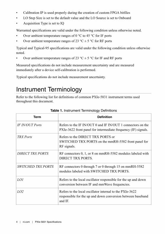
Instrument TerminologyRefer to the following list for definitions of common PXIe-5831 instrument terms usedthroughout this document.
Table 1. Instrument Terminology Definitions
Term Definition
IF IN/OUT Ports Refers to the IF IN/OUT 0 and IF IN/OUT 1 connectors on thePXIe-3622 front panel for intermediate frequency (IF) signals.
TRX Ports Refers to the DIRECT TRX PORTS orSWITCHED TRX PORTS on the mmRH-5582 front panel forRF signals.
DIRECT TRX PORTS RF connectors 0, 1, or 8 on mmRH-5582 modules labeled withDIRECT TRX PORTS.
SWITCHED TRX PORTS RF connectors 0 through 7 or 0 through 15 on mmRH-5582modules labeled with SWITCHED TRX PORTS.
LO1 Refers to the local oscillator responsible for the up and downconversion between IF and mmWave frequencies.
LO2 Refers to the local oscillator internal to the PXIe-3622responsible for the up and down conversion between basebandand IF.
4 | ni.com | PXIe-5831 Specifications
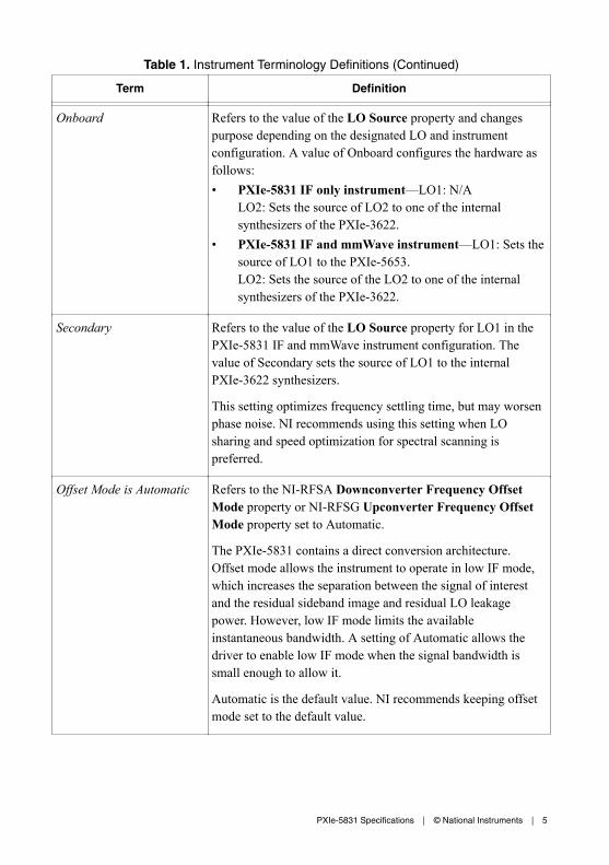
Table 1. Instrument Terminology Definitions (Continued)
Term Definition
Onboard Refers to the value of the LO Source property and changespurpose depending on the designated LO and instrumentconfiguration. A value of Onboard configures the hardware asfollows:• PXIe-5831 IF only instrument—LO1: N/A
LO2: Sets the source of LO2 to one of the internalsynthesizers of the PXIe-3622.
• PXIe-5831 IF and mmWave instrument—LO1: Sets thesource of LO1 to the PXIe-5653.LO2: Sets the source of the LO2 to one of the internalsynthesizers of the PXIe-3622.
Secondary Refers to the value of the LO Source property for LO1 in thePXIe-5831 IF and mmWave instrument configuration. Thevalue of Secondary sets the source of LO1 to the internalPXIe-3622 synthesizers.
This setting optimizes frequency settling time, but may worsenphase noise. NI recommends using this setting when LOsharing and speed optimization for spectral scanning ispreferred.
Offset Mode is Automatic Refers to the NI-RFSA Downconverter Frequency OffsetMode property or NI-RFSG Upconverter Frequency OffsetMode property set to Automatic.
The PXIe-5831 contains a direct conversion architecture.Offset mode allows the instrument to operate in low IF mode,which increases the separation between the signal of interestand the residual sideband image and residual LO leakagepower. However, low IF mode limits the availableinstantaneous bandwidth. A setting of Automatic allows thedriver to enable low IF mode when the signal bandwidth issmall enough to allow it.
Automatic is the default value. NI recommends keeping offsetmode set to the default value.
PXIe-5831 Specifications | © National Instruments | 5

Table 1. Instrument Terminology Definitions (Continued)
Term Definition
Offset Mode is Enabled Refers to the NI-RFSA Downconverter Frequency OffsetMode property or NI-RFSG Upconverter Frequency OffsetMode property set to Enabled.
The PXIe-5831 contains a direct conversion architecture.Offset mode allows the instrument to operate in low IF mode,which increases the separation between the signal of interestand the residual sideband image and residual LO leakagepower.
Offset Mode is User-Defined
Refers to the NI-RFSA Downconverter Frequency OffsetMode property or NI-RFSG Upconverter Frequency OffsetMode property set to User-Defined.
The PXIe-5831 contains a direct conversion architecture.Offset Mode set to User-Defined allows the instrument tooperate with maximum instantaneous bandwidth. By default,the offset is selected to maximize the available instantaneousbandwidth.
dBr For receivers, dBr refers to the power of a received signal withrespect to the instrument's configured reference level. Forexample, if the reference level is set to -10 dBm but thereceived tone is -7 dBr, the actual power of the received CW is-17 dBm.
For transmitters, dBr refers to the generated power of a CWwith respect to the instrument's peak power setting. Forexample, with a peak power level setting of +5 dBm and a-3 dBr setting, the power of the transmitted CW is +2 dBm.
Related Information
Refer to the PXIe-5831 section of the NI RF Vector Signal Transceivers Help for moreinformation about instrument terminology.
6 | ni.com | PXIe-5831 Specifications

FrequencyFrequency range1
IF IN/OUT 0, IF IN/OUT 1 5 GHz to 21 GHz
TRX ports2 (Transmit) 22.5 GHz to 31.3 GHz37 GHz to 44 GHz
TRX ports2 (Receive) 22.5 GHz to 44 GHz
Frequency bandwidth 1 GHz within the specified frequency rangesTuning resolution3 4.45 uHz
Table 2. Default LO Step Size4,5
Frequency Range Step Size
Onboard Secondary
5 GHz to 14.2 GHz 2 MHz —
>14.2 GHz to 21 GHz 4 MHz —
22.5 GHz to 44 GHz <1 Hz 8 MHz
1 Frequency range refers to the range of upconverter or downconverter center frequencies. Theactual frequency coverage extends beyond the upconverter or downconverter frequency by up tohalf of the frequency bandwidth.
2 The mmRH-5582 DIRECT TRX PORTS and SWITCHED TRX PORTS share the same frequencyranges and are only available on the PXIe-5831 mmWave instrument configurations.
3 Tuning resolution combines LO step size capability and frequency shift DSP implemented on theFPGA.
4 The worst case LO spurious content degrades for smaller LO step sizes and improves for larger LOstep sizes that are multiples of 2 MHz and 10 MHz.
5 LO step size can be set using the driver software.
PXIe-5831 Specifications | © National Instruments | 7

Frequency Settling Time
Table 3. PXIe-5653 Frequency Lock Time,6 Typical
Frequency Step Size Frequency Lock Time (ms)
≤25 MHz 0.85
≤50 MHz 1.10
≤75 MHz 1.35
≤80 MHz 1.35
≤90 MHz 1.35
≤100 MHz 1.35
≤250 MHz 1.80
≤500 MHz 6
≤1.0 GHz 10
≤2.0 GHz 13
≤3.0 GHz 15
≤5.1 GHz 17
6 LO1 Frequency Tuning Time consists of the PXIe-5653 Lock Time + PXIe-5831 (LO1) SettlingTime to Required Accuracy. The PXIe-5653 Lock Time is dependent on the RF Center Frequency(CF) frequency step change from initial frequency to final frequency. The relationship between theCF and the PXIe-5653 frequency is governed by the equation: F_PXIe-5653 = (FCF + FIF)/8. FIF isdetermined by the CF. For CF = 22.5 GHz to 31.3 GHz, FIF = 17.8 GHz; CF = >31.3 GHz to40 GHz, FIF = 12 GHz; CF = >40 GHz to 44 GHz, FIF = 9 GHz For example, for a CF step changefrom 28 GHz to 39 GHz, first calculate the equivalent FPXIe-5653 for 28 GHz, which is 5.725 GHz,then the equivalent CF frequency for 39 GHz, which is 6.375 GHz. The PXIe-5653 step size is6.375 GHz - 5.725 GHz = 650 MHz. The corresponding PXIe-5653 maximum frequency lock timeis 10 ms.
8 | ni.com | PXIe-5831 Specifications
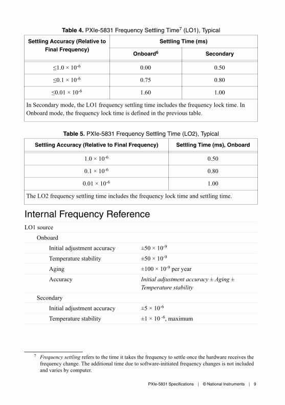
Table 4. PXIe-5831 Frequency Settling Time7 (LO1), Typical
Settling Accuracy (Relative toFinal Frequency)
Settling Time (ms)
Onboard6 Secondary
≤1.0 × 10⁻⁶ 0.00 0.50
≤0.1 × 10⁻⁶ 0.75 0.80
≤0.01 × 10⁻⁶ 1.60 1.00
In Secondary mode, the LO1 frequency settling time includes the frequency lock time. InOnboard mode, the frequency lock time is defined in the previous table.
Table 5. PXIe-5831 Frequency Settling Time (LO2), Typical
Settling Accuracy (Relative to Final Frequency) Settling Time (ms), Onboard
1.0 × 10⁻⁶ 0.50
0.1 × 10⁻⁶ 0.80
0.01 × 10⁻⁶ 1.00
The LO2 frequency settling time includes the frequency lock time and settling time.
Internal Frequency ReferenceLO1 source
Onboard
Initial adjustment accuracy ±50 × 10-9
Temperature stability ±50 × 10-9
Aging ±100 × 10-9 per year
Accuracy Initial adjustment accuracy ± Aging ±Temperature stability
Secondary
Initial adjustment accuracy ±5 × 10⁻⁶
Temperature stability ±1 × 10 -6, maximum
7 Frequency settling refers to the time it takes the frequency to settle once the hardware receives thefrequency change. The additional time due to software-initiated frequency changes is not includedand varies by computer.
PXIe-5831 Specifications | © National Instruments | 9

Aging ±1 × 10⁻⁶ per year, maximum
Accuracy Initial adjustment accuracy ± Aging ±Temperature stability
LO2 source (Onboard)
Initial adjustment accuracy ±5 × 10⁻⁶
Temperature stability ±1 × 10 -6, maximum
Aging ±1 × 10⁻⁶ per year, maximum
Accuracy Initial adjustment accuracy ± Aging ±Temperature stability
Spectral Purity
Table 6. IF Single Sideband Phase Noise (IF IN/OUT Ports), Typical
Frequency Phase Noise (dBc/Hz, Single Sideband)
5 GHz to 7.1 GHz -103
>7.1 GHz to 14.2 GHz -97
>14.2 GHz to 21 GHz -95
Conditions: 20 kHz offset; module temperatures within ± 5 °C of last self-calibrationtemperature; LO2 LO Source: Onboard.
Table 7. RF Single Sideband Phase Noise (Direct/Switched TRX Ports), Typical
Frequency Phase Noise (dBc/Hz, Single Sideband)
Onboard Secondary
22.5 GHz to 31.3 GHz -97 -86
>31.3 GHz to 40 GHz -99 -86
40 GHz to 44 GHz -103 -85
Conditions: 20 kHz offset; module temperatures within ± 5 °C of last self-calibrationtemperature; LO1 LO Source: Onboard or Secondary.
10 | ni.com | PXIe-5831 Specifications

Figure 1. Onboard LO2 Phase Noise at 5.5 GHz, 10 GHz, and 18 GHz, Measured(Spurs Not Shown)
–50
–150
–140
–130
–120
–110
–100
–80
–70
–60
100 M100 1 k 10 k 100 k 1 M 10 M–160
10Frequency Offset (Hz)
Pha
se N
oise
(dB
c/H
z)
–90
18 GHz
5.5 GHz10 GHz
Figure 2. Onboard LO1 Phase Noise at 28 GHz and 39 GHz, Measured8 (Spurs NotShown)
–50
–150
–140
–130
–120
–110
–100
–80
–70
–60
100 M100 1 k 10 k 100 k 1 M 10 M–160
10Frequency Offset (Hz)
Pha
se N
oise
(dB
c/H
z)
–90
28 GHz39 GHz
8 LO1 LO Source property is set to Onboard.
PXIe-5831 Specifications | © National Instruments | 11

Transmit (IF IN/OUT Ports)
IF Output Amplitude Range
Table 8. IF Output Maximum Power (dBm), CW
Upconverter CenterFrequency
Leveled Power, Specification Unleveled Power, Typical
IF0 IF1 IF0 IF1
5 GHz to 8 GHz 12 12 17 16
>8 GHz to 12 GHz 12 12 15 14
>12 GHz to 18 GHz 12 12 15 14
>18 GHz to 21 GHz 8 7 10 9
Conditions: Valid over 23 °C ± 5 °C with the last self-calibration performed at 23°C.
Measured with a tone 10 MHz offset from upconverter center frequency. For 0 °C to 45 °C,the leveled power specification output powers are 3 dB less than that of 23 °C ± 5 °C.
Minimum output power Noise floor
Output attenuator (analog power)resolution
1 dB, nominal
Digital attenuation resolution9 <0.1 dB
9 Average output power ≥ -40 dBm.
12 | ni.com | PXIe-5831 Specifications

Figure 3. IF Output Maximum CW Average Power, Measured
178 976 10 11 12 13 15 16 18 2014 19
13
14
15
16
17
18
19
21
23
22
25
24
12
Upconverter Center Frequency (GHz)
Ave
rage
Pow
er (
dBm
)
20
5 21
26
21
Ave
rage
Pow
er (
dBm
)
IF1 Maximum Port PowerIF0 Maximum Port Power
IF Output Amplitude Settling Time10
<0.5 dB of final value 27 µs, nominal
<0.1 dB of final value 40 µs, nominal
IF Output Amplitude Accuracy
Table 9. IF Output Absolute Amplitude Accuracy (dB) (Offset Mode is User-Defined)
UpconverterCenter
Frequency
23 °C ± 5 °C 0 °C to 45 °C
Specification Typical-95 Typical Specification
5 GHz to 8 GHz ±1.2 ±0.8 ±0.5 ±1.9
>8 GHz to 12 GHz ±1.4 ±1.0 ±0.6 ±2.1
>12 GHz to18 GHz
±1.8 ±1.4 ±0.8 ±2.7
10 Refers to the time it takes to switch between two analog gain states with frequency unchanged oncethe hardware receives the amplitude change. The additional time due to software-initiatedamplitude changes is not included and varies by computer. When changing frequencies,reconfiguration time is dominated by the frequency settling. Refer to Frequency Settling Time formore information.
PXIe-5831 Specifications | © National Instruments | 13

Table 9. IF Output Absolute Amplitude Accuracy (dB) (Offset Mode is User-Defined) (Continued)
UpconverterCenter
Frequency
23 °C ± 5 °C 0 °C to 45 °C
Specification Typical-95 Typical Specification
>18 GHz to21 GHz
±2.1 ±1.7 ±1.0 ±2.9
Conditions: Peak power level -30 dBm to IF Output maximum leveled power specification;measured with a CW signal at 10 MHz offset from the configured upconverter centerfrequency; Upconverter/Downconverter Frequency Offset Mode: User-Defined;measurement performed after the PXIe-5831 has settled.
This specification is valid only when the instrument is operating within the specified ambienttemperature range and each module is within ±5 °C from the last self-calibrationtemperature, as measured with its onboard temperature sensors.
Table 10. IF Output Absolute Amplitude Accuracy (dB) (Offset Mode is Enabled)
UpconverterCenter
Frequency
23 °C ± 5 °C 0 °C to 45 °C
Specification Typical-95 Typical Specification
5 GHz to 8 GHz ±1.2 ±0.8 ±0.5 ±2.0
>8 GHz to 12 GHz ±1.4 ±1.0 ±0.6 ±2.1
>12 GHz to18 GHz
±1.8 ±1.4 ±0.8 ±2.7
>18 GHz to21 GHz
±2.1 ±1.7 ±1.0 ±2.9
Conditions: Peak power level -30 dBm to IF Output maximum leveled power specification;measured with a CW signal at I/Q center frequency, where I/Q center frequency is offset257.5 MHz offset from the configured upconverter center frequency where the driverautomatically applies a 257.5 MHz offset for signals with 450 MHz bandwidth or less.Upconverter/Downconverter Frequency Offset Mode: Enabled; measurement performedafter the PXIe-5831 has settled.
This specification is valid only when the instrument is operating within the specified ambienttemperature range and each module is within ±5 °C from the last self-calibrationtemperature, as measured with its onboard temperature sensors.
14 | ni.com | PXIe-5831 Specifications

Table 11. IF Output Relative Amplitude Accuracy, Typical (Offset Mode is User-Defined)
Upconverter Center Frequency Relative Amplitude Accuracy (dB)
5 GHz to 8 GHz ±0.25
>8 GHz to 12 GHz ±0.30
>12 GHz to 18 GHz ±0.40
>18 GHz to 21 GHz ±0.40
Conditions: Peak power level -30 dBm to IF Output maximum leveled power specification;measured with a CW signal at 10 MHz offset from the configured upconverter centerfrequency; Upconverter/Downconverter Frequency Offset Mode: User-Defined;measurement performed after the PXIe-5831 has settled.
Relative accuracy describes the residual absolute accuracy error when compared to theabsolute accuracy error at 0 dBm.
This specification is valid only when the instrument is operating within the specified ambienttemperature range and each module is within ±5 °C from the last self-calibrationtemperature, as measured with its onboard temperature sensors.
Table 12. IF Output Relative Amplitude Accuracy (Offset Mode is Enabled), Typical
Upconverter Center Frequency Relative Amplitude Accuracy (dB)
5 GHz to 8 GHz ±0.25
>8 GHz to 12 GHz ±0.30
>12 GHz to 18 GHz ±0.40
>18 GHz to 21 GHz ±0.40
Conditions: Peak power level -30 dBm to IF Output maximum leveled power specification;measured with a CW signal at I/Q center frequency, where I/Q center frequency is offset257.5 MHz offset from the configured upconverter center frequency; Upconverter/Downconverter Frequency Offset Mode: Enabled; measurement performed after thePXIe-5831 has settled.
Relative accuracy describes the residual absolute accuracy error when compared to theabsolute accuracy error at 0 dBm.
This specification is valid only when the instrument is operating within the specified ambienttemperature range and each module is within ±5 °C from the last self-calibrationtemperature, as measured with the onboard temperature sensors.
PXIe-5831 Specifications | © National Instruments | 15

IF Output Frequency Response
Table 13. IF Output Frequency Response (dB)
UpconverterCenter
Frequency
23 °C ± 5 °C 0 °C to 45 °C
Specification Typical-95 Typical Specification
5 GHz to 8 GHz 1.45 0.95 0.80 1.90
>8 GHz to 12 GHz 1.45 0.85 0.75 1.95
>12 GHz to18 GHz
1.70 1.10 0.95 2.25
>18 GHz to21 GHz
1.95 1.30 1.10 2.55
Conditions: Peak power level -30 dBm to IF Output maximum leveled power specification;module temperature within ±5 °C of last self-calibration temperature.
Frequency response is defined as the maximum relative amplitude deviation from thereference offset frequency over the instantaneous bandwidth. For the PXIe-5831 IF output,the reference offset frequency is 10 MHz higher than the upconverter center frequency. Forthe absolute amplitude accuracy at the reference offset, refer to the IF Output AmplitudeAccuracy section.
Figure 4. IF Output Frequency Response, 0 dBm, Peak Output Power Level, Equalized,Measured
1
–0.6
–0.2
0.6
5000–1
–500Frequency Offset (MHz)
Am
plitu
de (
dB)
–0.4
0.2
0
0.8
0.4
–0.8
–400 –300 –200 –100 200100 300 400
5.5 GHz7.2 GHz10 GHz18 GHz
16 | ni.com | PXIe-5831 Specifications

Figure 5. Maximum IF Output Frequency Response Deviation versus UpconverterCenter Frequency, Measured
1
0.5
0.7
0.9
21140
5Upconverter Center Frequency (GHz)
Max
imum
Fre
quen
cy R
espo
nse
Dev
iatio
n (d
B)
0.6
0.8
0.2
0.4
0.1
0.3
6 8 10 12 157 9 11 13 1716 18 19 20
15 dBm0 dBm–15 dBm–30 dBm
IF Output Average Noise Density
Table 14. Output Average Noise Density (dBm/Hz), Typical
Upconverter CenterFrequency
Output Power Level Setting
-10 dBm 0 dBm 15 dBm
5 GHz to 8 GHz -156 -149 -135
>8 GHz to 12 GHz -154 -148 -135
>12 GHz to 18 GHz -151 -145 -132
>18 GHz to 21 GHz -149 -145 -131
Conditions: 10 averages; 40 dB baseband signal attenuation; noise measurement frequencyoffset by 200 MHz from the upconverter center frequency; the instrument driver is in peakmode.
Measured on the PXIe-3622 IF IN/OUT 1 port. The IF IN/OUT 0 port has a 1 dB to 5 dBdegradation compared to the IF IN/OUT 1 port.
PXIe-5831 Specifications | © National Instruments | 17

IF Output Third-Order Intermodulation
Table 15. IF Output Third-Order Intermodulation Distortion (IMD3) (dBc), Typical
UpconverterCenter
Frequency
IF IN/OUT 0 IF IN/OUT 1
Output Power Level Setting Output Power Level Setting
-30 dBm 0 dBm 15 dBm -30 dBm 0 dBm 15 dBm
5 GHz to 8 GHz -56 -56 -49 -45 -46 -46
>8 GHz to12 GHz
-58 -57 -41 -53 -52 -39
>12 GHz to18 GHz
-55 -55 -37 -53 -50 -35
>18 GHz to21 GHz
-55 -54 — -50 -50 —
Conditions: Measured by generating two -7 dBr tones at +95 MHz and +105 MHz off fromthe upconverter center frequency. The nominal peak envelope power is 1 dB below theOutput Power Level Setting; the instrument driver is in peak mode.
IF Output Harmonic Spurs
Table 16. IF Output Out of Band Spur Levels, Measured
Upconverter Center Frequency Harmonic Level (dBc)
5 GHz to 8 GHz -32
>8 GHz to 12 GHz -34
>12 GHz to 21 GHz -34
>18 GHz to 21 GHz -48
Conditions: Peak power level 0 dBm; measured with a CW signal at 100 MHz offset fromthe configured upconverter center frequency; Upconverter/Downconverter Frequency OffsetMode: User-Defined; measurement performed after the PXIe-5831 has settled.
Includes CW and LO harmonics.
Measured at 23 °C ambient within ±5 °C from the last self-calibration temperature.
18 | ni.com | PXIe-5831 Specifications

IF Output Nonharmonic Spurs
Table 17. IF Output Nonharmonic Spurs (dBc) (Default LO Step Size), Typical
Upconverter CenterFrequency
Offset ≤ 500 kHz 500 kHz < Offset≤ 20 MHz
Offset > 20 MHz
5 GHz to 8 GHz -62 -44 <-70
>8 GHz to 12 GHz -59 -51 <-70
>12 GHz to 18 GHz -54 -51 <-70
>18 GHz to 21 GHz -53 -59 <-70
Conditions: Measured relative to a 0 dBm output tone.
The maximum offset is limited to the instantaneous 1 GHz bandwidth at the referencedupconverter center frequency.
Note Offset refers to ± desired signal offset (Hz) around the current upconvertercenter frequency.
Table 18. IF Output Nonharmonic Spurs (dBc) (1 MHz LO Step Size), Measured
Upconverter Center Frequency 0 Hz ≤ Offset ≤ 5 MHz
5 GHz to 7.1 GHz -64
>7.1 GHz to 14.2 GHz -46
>14.2 GHz to 21 GHz -40
Conditions: Measured relative to a 0 dBm output tone.
Note Offset refers to ± desired signal offset (Hz) around the current upconvertercenter frequency.
IF Output LO Residual Power
Table 19. IF Output LO Residual Power (dBr), Typical
Upconverter CenterFrequency
Self-Calibration °C ± 1 °C Self-Calibration °C ± 5 °C
5 GHz to 8 GHz -50 -47
>8 GHz to 12 GHz -48 -36
PXIe-5831 Specifications | © National Instruments | 19
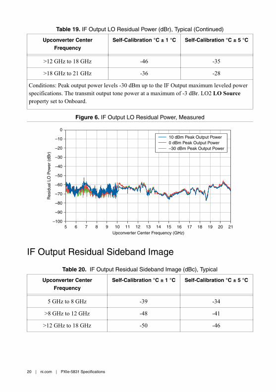
Table 19. IF Output LO Residual Power (dBr), Typical (Continued)
Upconverter CenterFrequency
Self-Calibration °C ± 1 °C Self-Calibration °C ± 5 °C
>12 GHz to 18 GHz -46 -35
>18 GHz to 21 GHz -36 -28
Conditions: Peak output power levels -30 dBm up to the IF Output maximum leveled powerspecifications. The transmit output tone power at a maximum of -3 dBr. LO2 LO Sourceproperty set to Onboard.
Figure 6. IF Output LO Residual Power, Measured
0
–90
–80
–70
–60
–50
–40
–20
–10
2115–100
5Upconverter Center Frequency (GHz)
Res
idua
l LO
Pow
er (
dBr)
–30
7 9 1311 1817 19 20
10 dBm Peak Output Power0 dBm Peak Output Power–30 dBm Peak Output Power
146 8 1210 16
IF Output Residual Sideband Image
Table 20. IF Output Residual Sideband Image (dBc), Typical
Upconverter CenterFrequency
Self-Calibration °C ± 1 °C Self-Calibration °C ± 5 °C
5 GHz to 8 GHz -39 -34
>8 GHz to 12 GHz -48 -41
>12 GHz to 18 GHz -50 -46
20 | ni.com | PXIe-5831 Specifications
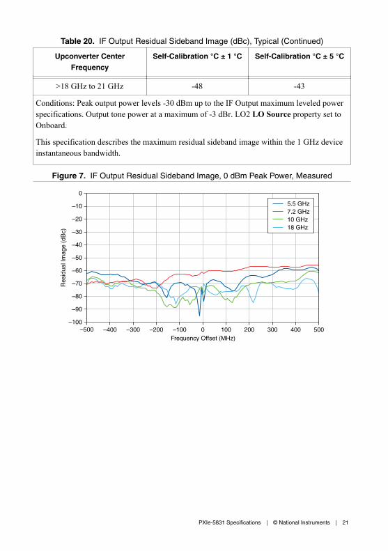
Table 20. IF Output Residual Sideband Image (dBc), Typical (Continued)
Upconverter CenterFrequency
Self-Calibration °C ± 1 °C Self-Calibration °C ± 5 °C
>18 GHz to 21 GHz -48 -43
Conditions: Peak output power levels -30 dBm up to the IF Output maximum leveled powerspecifications. Output tone power at a maximum of -3 dBr. LO2 LO Source property set toOnboard.
This specification describes the maximum residual sideband image within the 1 GHz deviceinstantaneous bandwidth.
Figure 7. IF Output Residual Sideband Image, 0 dBm Peak Power, Measured
0
–90
–80
–70
–60
–50
–40
–20
–10
5000–100
–500Frequency Offset (MHz)
Res
idua
l Im
age
(dB
c) –30
–400 –300 –100–200 200100 300 400
5.5 GHz7.2 GHz10 GHz18 GHz
PXIe-5831 Specifications | © National Instruments | 21

Figure 8. Maximum IF Output Residual Sideband Image Versus Upconverter CenterFrequency, Measured
0
–90
–80
–70
–60
–50
–40
–20
–10
2115–100
5Upconverter Center Frequency (GHz)
Max
imum
Res
idua
l Im
age
(dB
c)
–30
7 9 1311 1817 19 20
10 dBm Peak Output Power Setting0 dBm Peak Output Power Setting–30 dBm Peak Output Power Setting
146 8 1210 16
Transmit (TRX Ports)
RF Output Amplitude Range
Table 21. RF Output Maximum Power (dBm), CW
Upconverter CenterFrequency
Leveled Power, Specification Unleveled Power, Typical
Direct TRXPorts
Switched TRXPorts
Direct TRXPorts
Switched TRXPorts
22.5 GHz to <24 GHz 10 6 14 10
24 GHz to 31.3 GHz 10 6 15 10
37 GHz to 40 GHz 6 0 11 7
22 | ni.com | PXIe-5831 Specifications
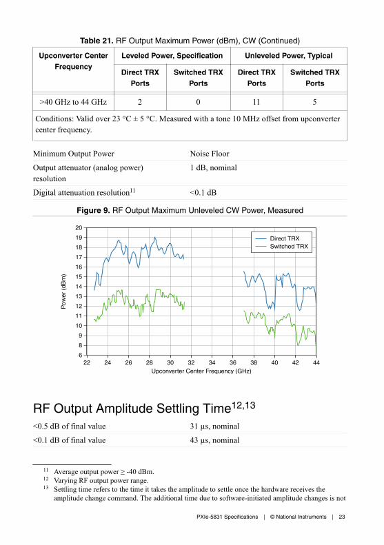
Table 21. RF Output Maximum Power (dBm), CW (Continued)
Upconverter CenterFrequency
Leveled Power, Specification Unleveled Power, Typical
Direct TRXPorts
Switched TRXPorts
Direct TRXPorts
Switched TRXPorts
>40 GHz to 44 GHz 2 0 11 5
Conditions: Valid over 23 °C ± 5 °C. Measured with a tone 10 MHz offset from upconvertercenter frequency.
Minimum Output Power Noise Floor
Output attenuator (analog power)resolution
1 dB, nominal
Digital attenuation resolution11 <0.1 dB
Figure 9. RF Output Maximum Unleveled CW Power, Measured
10
15
20
446
8
22Upconverter Center Frequency (GHz)
Po
wer
(dB
m)
18
13
17
19
26 30 4224 28 34
9
14
12
16
11
32 3836 40
Direct TRXSwitched TRX
RF Output Amplitude Settling Time12,13
<0.5 dB of final value 31 µs, nominal
<0.1 dB of final value 43 µs, nominal
11 Average output power ≥ -40 dBm.12 Varying RF output power range.13 Settling time refers to the time it takes the amplitude to settle once the hardware receives the
amplitude change command. The additional time due to software-initiated amplitude changes is not
PXIe-5831 Specifications | © National Instruments | 23
RF Output Amplitude Accuracy
Table 22. RF Output Absolute Amplitude Accuracy (dB) (Offset Mode is User-Defined)
Upconverter CenterFrequency Specification Typical-95 Typical
22.5 GHz to 31.3 GHz ±2.1 ±1.6 ±1.1
37 GHz to 40 GHz ±2.2 ±1.9 ±1.2
>40 GHz to 44 GHz ±3.0 ±2.2 ±1.5
Conditions: Valid for RF output power levels from -40 dBm up to the RF Output maximumleveled power specifications for direct and switched ports; measured with a CW signal at10 MHz offset from the configured upconverter center frequency; Upconverter/Downconverter Frequency Offset Mode: User- Defined; measurement performed after thePXIe-5831 has settled.
This specification is valid over 23 °C ± 5 °C with the last self-calibration performed at 23°C.
Table 23. RF Output Absolute Amplitude Accuracy (dB) (Offset Mode is Enabled),Typical
Upconverter Center Frequency Direct TRX (dB) Switched TRX (dB)
22.5 GHz to 31.3 GHz ±1.1 ±1.4
37 GHz to 40 GHz ±1.2 ±1.2
>40 GHz to 44 GHz ±1.5 ±1.8
Conditions: Valid for RF output power levels from -40 dBm up to the RF Output maximumleveled power specifications for direct and switched ports; measured with a CW signal at I/Qcenter frequency, where I/Q center frequency is offset 257.5 MHz offset from the configuredupconverter center frequency where the driver automatically applies a 257.5 MHz offset forsignals with 450 MHz bandwidth or less; Upconverter/Downconverter Frequency OffsetMode: Enabled; measurement performed after the PXIe-5831 has settled.
This specification is valid over 23 °C ± 5 °C with the last self-calibration performed at 23°C.
included and varies by computer. When changing frequencies, reconfiguration time is dominatedby the frequency settling. Refer to Frequency Settling Time for more information.
24 | ni.com | PXIe-5831 Specifications

Table 24. RF Output Relative Amplitude Accuracy (Offset Mode is User-Defined),Typical
Upconverter Center Frequency Direct TRX (dB) Switched TRX (dB)
22.5 GHz to 31.3 GHz ±0.50 ±0.75
37 GHz to 40 GHz ±0.55 ±0.80
>40 GHz to 44 GHz ±0.60 ±0.85
Conditions: Valid for RF output power levels from -40 dBm up to the RF Output maximumleveled power specifications for direct and switched ports; measured with a CW signal at10 MHz offset from the configured upconverter center frequency; Upconverter/Downconverter Frequency Offset Mode: User- Defined; measurement performed after thePXIe-5831 has settled.
Relative accuracy describes the residual absolute accuracy error when compared to theabsolute accuracy error at 0 dBm.
This specification is valid only when the instrument is operating within the specified ambienttemperature range and each module is within ±5 °C from the last self-calibrationtemperature, as measured with its onboard temperature sensors.
Table 25. RF Output Relative Amplitude Accuracy (Offset Mode is Enabled), Typical
Upconverter Center Frequency Direct TRX (dB) Switched TRX (dB)
22.5 GHz to 31.3 GHz ±0.6 ±0.8
37 GHz to 40 GHz ±0.55 ±0.8
>40 GHz to 44 GHz ±0.75 ±0.9
Conditions: Valid for RF output power levels from -40 dBm up to the RF Output maximumleveled power specifications for direct and switched ports; ; measured with a CW signal atI/Q center frequency, where I/Q center frequency is offset 257.5 MHz offset from theconfigured upconverter center frequency; Upconverter/Downconverter Frequency OffsetMode: Enabled; measurement performed after the PXIe-5831 has settled.
Relative accuracy describes the residual absolute accuracy error when compared to theabsolute accuracy error at 0 dBm.
This specification is valid only when the instrument is operating within the specified ambienttemperature range and each module is within ±5 °C from the last self-calibrationtemperature, as measured with its onboard temperature sensors.
PXIe-5831 Specifications | © National Instruments | 25

RF Output Frequency Response
Table 26. RF Output Frequency Response (dB)
Upconverter CenterFrequency Specification Typical-95 Typical
22.5 GHz to 23 GHz 2.8 2.4 1.1
>23 GHz to 31.3 GHz 2.2 1.8 1.0
37 GHz to 40 GHz 2.3 1.9 1.1
>40 GHz to 44 GHz 2.8 2.6 1.4
Conditions: Valid for RF output power levels from -35 dBm up to the RF Output maximumleveled power specifications for direct and switched ports.
This specification is valid only when the instrument is operating within the specified ambienttemperature range and each module is within ±5 °C from the last self-calibrationtemperature, as measured with its onboard temperature sensors.
Frequency response is defined as the maximum relative amplitude deviation from thereference offset frequency. For the PXIe-5831 RF output, the reference offset frequency is10 MHz higher than the upconverter center frequency over the instantaneous bandwidth. Forthe absolute amplitude accuracy at the reference offset, refer to the RF Output AmplitudeAccuracy section.
Figure 10. Direct TRX RF Output Frequency Response, 0 dBm, Peak Output PowerLevel, Equalized, Measured
1.5
–1
–0.2
0.8
1.2
500–1.5
–500Frequency Offset (MHz)
Am
plitu
de (
dB) 0.4
–0.6
0.2
1
0.6
–300 –100 400100–400 –200 200 3000
–1.2
–0.4
–0.8
0
22.5 GHz28 GHz39 GHz43.5 GHz
26 | ni.com | PXIe-5831 Specifications

Figure 11. Direct TRX Maximum RF Output Frequency Response Deviation versusUpconverter Center Frequency, Measured
1.5
0.2
0.7
1.2
1.4
440
22Upconverter Center Frequency (GHz)
Max
imum
Fre
quen
cy R
espo
nse
Dev
iatio
n (d
B)
1
0.5
0.9
1.3
1.1
26 30 4224 28 38
0.1
0.6
0.4
0.8
0.3
23 27 31 4325 29 37 4039 41
. . .
. . .
+15 dBm (22.5 GHz to 31.3 GHz)+5 dBm0 dBm–15 dBm–30 dBm
Figure 12. Switched RF Output Frequency Response Deviation versus UpconverterCenter Frequency, Measured
1.5
0.25
0.5
0.75
1
1.25
44420
22Frequency (GHz)
Max
imum
Fre
quen
cy R
espo
nse
Dev
iatio
n (d
B)
26 30 3834 4024 28 3632
–30 dBm–15 dBm0 dBm
PXIe-5831 Specifications | © National Instruments | 27

RF Output Average Noise Density
Table 27. RF Output Average Noise Density (dBm/Hz), Measured
Upconverter CenterFrequency
Output Power Level Setting
-10 dBm 0 dBm +10 dBm (DirectTRX Ports Only)
22.5 GHz to 31.3 GHz -153 -143 -132
37 GHz to 40 GHz -153 -142 -131
>40 GHz to 44 GHz -152 -144 -132
Conditions: Measured at both switched and direct TRX ports, +10 dBm valid for direct TRXports only; 30 averages; 40 dB baseband signal attenuation; noise measurement frequencyoffset 200 MHz relative to the upconverter center frequency.
The instrument driver is in peak mode.
RF Output Third-Order Intermodulation
Table 28. Direct TRX RF Output Third-Order Intermodulation Distortion (IMD3) (dBc),Typical
Upconverter CenterFrequency
Output Power Level Setting
-20 dBm 0 dBm 10 dBm
22.5 GHz to 31.3 GHz -48 -45 -41
37 GHz to 40 GHz -54 -50 -36
>40 GHz to 44 GHz -49 -48 -37
Conditions: Measured by generating two -7 dBr tones applied at +95 MHz and +105 MHzoffset from the upconverter center frequency. The nominal peak envelope is 1 dB below theOutput Power Level Setting; the instrument driver is in peak mode.
28 | ni.com | PXIe-5831 Specifications

Table 29. Switched TRX RF Output Third-Order Intermodulation Distortion (IMD3)(dBc), Typical
Upconverter CenterFrequency
Output Power Level Setting
-30 dBm 0 dBm 5 dBm
22.5 GHz to 31.3 GHz -51 -47 -48
37 GHz to 40 GHz -59 -44 —
>40 GHz to 44 GHz -52 -39 —
Conditions: Measured by generating two -7 dBr tones applied at +95 MHz and +105 MHzoffset from the upconverter center frequency. The nominal peak envelope is 1 dB below theOutput Power Level Setting; the instrument driver is in peak mode. For >37 GHz, +5 dBm isoutside the leveled power range and was not measured.
RF Output LO Residual Power
Table 30. RF Output LO Residual Power (dBr), Typical
Upconverter CenterFrequency
Self-Calibration °C ± 1 °C Self-Calibration °C ± 5 °C
22.5 GHz to 31.3 GHz -48 -34
37 GHz to 40 GHz -50 -38
>40 GHz to 44 GHz -47 -34
Conditions: Peak output power levels -30 dBm up to the RF Output maximum leveled powerspecifications for direct and switched ports. The transmit tone power at a maximum of-3 dBr. LO1 and LO2 LO Source property set to Onboard. The values are with respect to thepeak power level setting, hence dBr.
PXIe-5831 Specifications | © National Instruments | 29

Figure 13. RF Output LO Residual Power at Direct TRX Port, Measured
4422 26 30 4224 28 3823 27 31 4325 29 37 4039 41. . .
. . .
0
–80
–30
–10
–100
Upconverter Center Frequency (GHz)
Res
idua
l LO
Pow
er (
dBr)
–50
–60
–20
–40
–90
–70
10 dBm Peak Output Power0 dBm Peak Output Power–30 dBm Peak Output Power
RF Output Residual Sideband Image
Table 31. RF Output Residual Sideband Image (dBc), Typical
Upconverter CenterFrequency
Self-Calibration °C ± 1 °C Self-Calibration °C ± 5 °C
22.5 GHz to 31.3 GHz -51 -41
37 GHz to 40 GHz -50 -44
>40 GHz to 44 GHz -45 -40
Conditions: Peak output power levels -30 dBm up to the RF Output maximum leveled powerspecifications for direct and switched ports. The transmit tone power at a maximum of -3dBr. LO1 and LO2 LO Source property set to Onboard.
This specification describes the maximum residual sideband image within the 1 GHz deviceinstantaneous bandwidth.
30 | ni.com | PXIe-5831 Specifications
Figure 14. RF Output Residual Sideband Image, 0 dBm Peak Power Setting at DirectTRX Port, Measured
0
–20
500–100
–500Frequency Offset (MHz)
Res
idua
l Im
age
(dB
c)
–60
–300 –100 400100–400 –200 200 3000
–40
–80
22.5 GHz28 GHz39 GHz43.5 GHz
Figure 15. Maximum RF Output Residual Sideband Image Versus Upconverter CenterFrequency at Direct TRX Port, Measured
0
–80
–30
–10
–100
Upconverter Center Frequency (GHz)
Res
idua
l Im
age
(dB
c)
–50
–60
–20
–40
–90
–70
4422 26 30 4224 28 3823 27 31 4325 29 37 4039 41. . .
. . .
10 dBm Peak Output Power0 dBm Peak Output Power–30 dBm Peak Output Power
PXIe-5831 Specifications | © National Instruments | 31
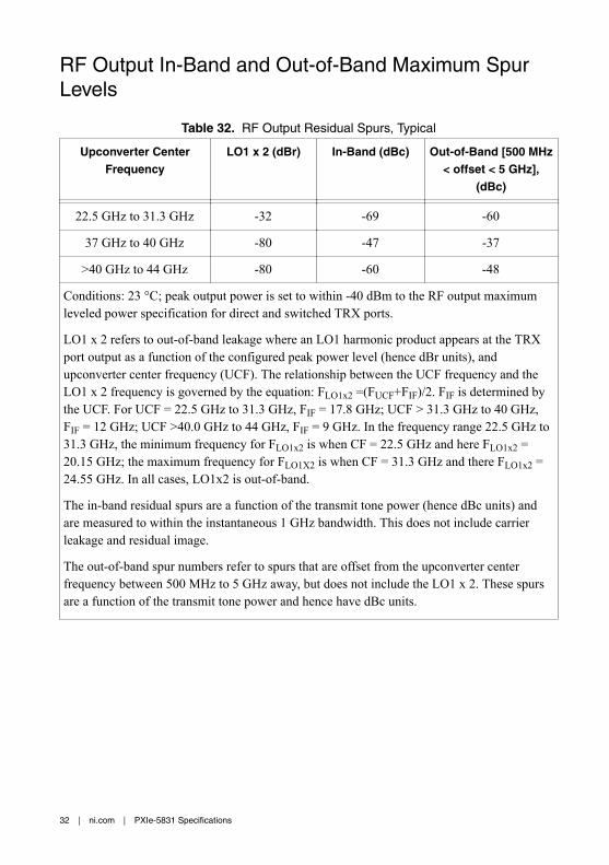
RF Output In-Band and Out-of-Band Maximum SpurLevels
Table 32. RF Output Residual Spurs, Typical
Upconverter CenterFrequency
LO1 x 2 (dBr) In-Band (dBc) Out-of-Band [500 MHz< offset < 5 GHz],
(dBc)
22.5 GHz to 31.3 GHz -32 -69 -60
37 GHz to 40 GHz -80 -47 -37
>40 GHz to 44 GHz -80 -60 -48
Conditions: 23 °C; peak output power is set to within -40 dBm to the RF output maximumleveled power specification for direct and switched TRX ports.
LO1 x 2 refers to out-of-band leakage where an LO1 harmonic product appears at the TRXport output as a function of the configured peak power level (hence dBr units), andupconverter center frequency (UCF). The relationship between the UCF frequency and theLO1 x 2 frequency is governed by the equation: FLO1x2 =(FUCF+FIF)/2. FIF is determined bythe UCF. For UCF = 22.5 GHz to 31.3 GHz, FIF = 17.8 GHz; UCF > 31.3 GHz to 40 GHz,FIF = 12 GHz; UCF >40.0 GHz to 44 GHz, FIF = 9 GHz. In the frequency range 22.5 GHz to31.3 GHz, the minimum frequency for FLO1x2 is when CF = 22.5 GHz and here FLO1x2 =20.15 GHz; the maximum frequency for FLO1X2 is when CF = 31.3 GHz and there FLO1x2 =24.55 GHz. In all cases, LO1x2 is out-of-band.
The in-band residual spurs are a function of the transmit tone power (hence dBc units) andare measured to within the instantaneous 1 GHz bandwidth. This does not include carrierleakage and residual image.
The out-of-band spur numbers refer to spurs that are offset from the upconverter centerfrequency between 500 MHz to 5 GHz away, but does not include the LO1 x 2. These spursare a function of the transmit tone power and hence have dBc units.
32 | ni.com | PXIe-5831 Specifications

Figure 16. RF TRX Output Residual Spurs (Out-of-band and In-band) vs UpconverterCenter Frequency, Measured14
0
–80
–70
–50
–30
–10
4442
–20
–40
–60
–9022
Upconverter Center Frequency (GHz)
Spu
r Le
vel (
dBc)
26 30 3834 4024 28 3632
Switched Port In-Band Spurs
Direct Port In-Band SpursSwitched Port Out-of-Band Spur
Direct Port Out-of-Band Spurs
Table 33. RF Output Second and Third Harmonics at Direct TRX port, Measured
Upconverter Center Frequency 2nd Harmonic (dBc) 3rd Harmonic (dBc)
22.5 GHz to 26 GHz -30 -105
>26 GHz to 31.3 GHz -90 -98
>37 GHz to 40 GHz -90 —
>40 GHz to 44 GHz -93 —
The RF Output power is set to +10 dBm. Includes CW harmonics only. For >37 GHz, the 3rdharmonic frequency is >110 GHz and outside the measured range.
Receive (IF IN/OUT Ports)
IF Input Amplitude RangeAmplitude range Average noise level to +20 dBm (CW RMS)
Gain resolution 1 dB, nominal
14 Does not show LO1 x 2, RF output residual LO leakage and RF output residual sideband image.
PXIe-5831 Specifications | © National Instruments | 33

Table 34. IF Input Analog Gain Range, Nominal
Downconverter Center Frequency IF Analog Gain Range (dB)
5 GHz to 8 GHz ≥61
>8 GHz to 12 GHz ≥57
>12 GHz to 18 GHz ≥58
>18 GHz to 21 GHz ≥57
IF Input Amplitude Settling Time15,16
<0.5 dB of final value 27 µs, nominal
<0.1 dB of final value 40 µs, nominal
IF Input Amplitude Accuracy
Table 35. IF Input Absolute Amplitude Accuracy (dB) (Offset Mode is User-Defined)
DownconverterCenter Frequency
23 °C ± 5 °C 0 °C to 45 °C
Specification Typical-95 Typical Specification
5 GHz to 8 GHz ±1.2 ±0.8 ±0.5 ±1.6
>8 GHz to 12 GHz ±1.4 ±1.0 ±0.7 ±1.6
>12 GHz to 18 GHz ±1.8 ±1.4 ±0.9 ±2.0
>18 GHz to 21 GHz ±2.0 ±1.5 ±0.9 ±2.6
Conditions: Reference level -30 dBm to 0 dBm for specification; -30 dBm to 20 dBm fortypical; measured with a CW signal at 10 MHz offset from the configured downconvertercenter frequency when a user-defined frequency offset is not applied; Upconverter/Downconverter Frequency Offset Mode: User-Defined; measurement performed after thePXIe-5831 has settled.
This specification is valid only when the instrument is operating within the specified ambienttemperature range and each module is within ±5 °C from the last self-calibrationtemperature, as measured with the onboard temperature sensors.
15 Constant RF input signal, varying input reference level.16 Settling time refers to the time it takes the amplitude to settle once the hardware receives the
amplitude change. The additional time due to software initiated amplitude changes is not includedand varies by computer. When changing frequencies, reconfiguration time is dominated by thefrequency settling. Refer to Frequency Settling Time for more information.
34 | ni.com | PXIe-5831 Specifications
Table 36. IF Input Absolute Amplitude Accuracy (dB) (Offset Mode is Enabled)
DownconverterCenter Frequency
23 °C ± 5 °C 0 °C to 45 °C
Specification Typical-95 Typical Specification
5 GHz to 8 GHz ±1.2 ±0.9 ±0.5 ±1.7
>8 GHz to 12 GHz ±1.4 ±1.0 ±0.7 ±1.9
>12 GHz to 18 GHz ±1.8 ±1.4 ±0.9 ±2.1
>18 GHz to 21 GHz ±2.0 ±1.5 ±0.9 ±2.6
Conditions: Reference level -30 dBm to 0 dBm for specification; -30 dBm to 20 dBm fortypical; measured with a CW signal at the I/Q center frequency, where the I/Q centerfrequency is 257.5 MHz offset from the configured downconverter center frequency wherethe driver automatically applies a 257.5 MHz offset for signals with 450 MHz bandwidth andless; Upconverter/Downconverter Frequency Offset Mode: Enabled; measurement performedafter the PXIe-5831 has settled.
This specification is valid only when the instrument is operating within the specified ambienttemperature range and each module is within ±5 °C from the last self-calibrationtemperature, as measured with the onboard temperature sensors.
Table 37. IF Input Relative Amplitude Accuracy (Offset Mode is User-Defined), Typical
Downconverter Center Frequency Relative Amplitude Accuracy (dB)
5 GHz to 8 GHz ±0.25
>8 GHz to 12 GHz ±0.40
>12 GHz to 18 GHz ±0.40
>18 GHz to 21 GHz ±0.40
Conditions: Reference level -30 dBm to +20 dBm; measured with a CW signal at 10 MHzoffset from the configured downconverter center frequency; Upconverter/DownconverterFrequency Offset Mode: User-Defined; measurement performed after the PXIe-5831 hassettled.
Relative accuracy describes the residual absolute accuracy error when compared to theabsolute accuracy at 0 dBm.
This specification is valid only when the instrument is operating within the specified ambienttemperature range and each module is within ±5 °C from the last self-calibrationtemperature, as measured with the onboard temperature sensors.
PXIe-5831 Specifications | © National Instruments | 35
Table 38. IF Input Relative Amplitude Accuracy (Offset Mode is Enabled), Typical
Downconverter Center Frequency Relative Amplitude Accuracy (dB)
5 GHz to 8 GHz ±0.25
>8 GHz to 12 GHz ±0.40
>12 GHz to 18 GHz ±0.40
>18 GHz to 21 GHz ±0.40
Conditions: Reference level -30 dBm to +20 dBm; measured with a CW signal at±257.5 MHz offset from the configured downconverter center frequency where the driverautomatically applies at the I/Q center frequency, where the I/Q center frequency is257.5 MHz offset for signals with 450 MHz bandwidth and less; Upconverter/Downconverter Frequency Offset Mode: Enabled; measurement performed after thePXIe-5831 has settled.
Relative accuracy describes the residual absolute accuracy error when compared to theabsolute accuracy at 0 dBm.
This specification is valid only when the instrument is operating within the specified ambienttemperature range and each module is within ±5 °C from the last self-calibrationtemperature, as measured with the onboard temperature sensors.
IF Input Frequency Response
Table 39. IF Input Frequency Response (dB)
DownconverterCenter Frequency
23 °C ± 5 °C 0 °C to 45 °C
Specification Typical-95 Typical Specification
5 GHz to 8 GHz 2.2 1.8 1.2 2.8
>8 GHz to 12 GHz 2.3 2.0 1.1 3.2
>12 GHz to 18 GHz 2.4 2.0 1.2 3.4
36 | ni.com | PXIe-5831 Specifications

Table 39. IF Input Frequency Response (dB) (Continued)
DownconverterCenter Frequency
23 °C ± 5 °C 0 °C to 45 °C
Specification Typical-95 Typical Specification
>18 GHz to 21 GHz 2.7 2.1 1.2 3.4
Conditions: Reference level -30 dBm to 0 dBm for specification; -30 dBm to 20 dBm fortypical; module temperatures within ±5 °C of last self-calibration temperature.
Frequency response is defined as the maximum relative amplitude deviation from thereference offset frequency over the instantaneous bandwidth. For the PXIe-5831 IF input, thereference offset frequency is 10 MHz higher than the downconverter center frequency. Forthe absolute amplitude accuracy at the reference offset, refer to the IF Input AmplitudeAccuracy section.
Figure 17. IF Input Frequency Response, 0 dBm, Reference Level, Equalized,Measured
1
–0.6
–0.2
0.2
0.6
5000–1
–500Frequency Offset (MHz)
Am
plitu
de (
dB)
–0.4
0
0.4
0.8
–0.8
–400 –300 –200 –100 200100 300 400
5.5 GHz7.2 GHz10 GHz18 GHz
PXIe-5831 Specifications | © National Instruments | 37

Figure 18. Maximum IF Input Frequency Response Deviation versus DownconverterCenter Frequency, Measured
1
0.1
0.3
0.5
0.9
216 130
5Downconverter Center Frequency (GHz)
Max
imum
Fre
quen
cy R
espo
nse
Dev
iatio
n (d
B)
0.7
0.2
0.4
0.6
0.8
7 8 9 10 11 12 14 15 16 17 18 19 20
20 dBm0 dBm–30 dBm
IF Input Average Noise Density
Table 40. Input Average Noise Density (dBm/Hz), Typical
Downconverter CenterFrequency -30 dBm Reference Level 0 dBm Reference Level
5 GHz to 8 GHz -162 -142
>8 GHz to 12 GHz -162 -142
>12 GHz to 18 GHz -159 -141
>18 GHz to 21 GHz -158 -141
Conditions: Input terminated with a 50 Ω load; 10 averages; noise measurement frequencyoffset by 6 MHz from the downconverter center frequency.
Measured on the PXIe-3622 IF IN/OUT 1 port. The IF IN/OUT 0 port has a 2 dBdegradation compared to the IF IN/OUT 1 port.
38 | ni.com | PXIe-5831 Specifications

IF Input Third-Order Intermodulation
Table 41. IF Input Third-Order Intercept Point (IIP3) (dBm), Typical
Downconverter CenterFrequency
Reference Level
-30 dBm 0 dBm 15 dBm
5 GHz to 8 GHz -6 20 35
>8 GHz to 12 GHz -4 19 33
>12 GHz to 18 GHz -7 20 33
>18 GHz to 21 GHz -7 16 31
Conditions: Measured with two -6 dBr tones applied at +95 MHz and +105 MHz offset fromthe downconverter center frequency.
IF Input Residual Spurs
Table 42. IF Input Residual Spurs (dBm), Typical
Downconverter CenterFrequency
60 kHz ≤ Offset< 60 MHz
Offset ≥ 60 MHz17
5 GHz to 8 GHz -74 -74
>8 GHz to 12 GHz -75 -75
>12 GHz to 18 GHz -73 -77
>18 GHz to 21 GHz -78 -78
Conditions : Reference level 0 dBm. Measured with the IF IN 1 port terminated with 50 Ω.
The maximum offset is limited to the instantaneous bandwidth at the referenceddownconverter center frequency.
Note Offset refers to ± desired signal offset (Hz) around the currentdownconverter center frequency.
17 The maximum offset is limited to within the equalized bandwidth of the referenced downconvertercenter frequency.
PXIe-5831 Specifications | © National Instruments | 39
IF Input LO Residual Power
Table 43. IF Input LO Residual Power (dBr18), Typical
Downconverter CenterFrequency
Self-Calibration °C ± 1 °C Self-Calibration °C ± 5 °C
5 GHz to 8 GHz -54 -44
>8 GHz to 12 GHz -47 -38
>12 GHz to 18 GHz -49 -38
>18 GHz to 21 GHz -44 -35
Conditions: Reference level is -30 dBm to +15 dBm. Input tone power at a maximum of-3 dBr. LO2 LO Source property set to Onboard.
Figure 19. IF Input LO Residual Power, Measured
0
–90
–80
–70
–60
–50
–40
–20
–10
2115–100
5Downconverter Center Frequency (GHz)
Res
idua
l LO
Pow
er (
dBr)
–30
7 9 1311 1817 19 20
20 dBm Reference Level0 dBm Reference Level–30 dBm Reference Level
146 8 1210 16
18 dBr is relative to the full scale of the configured reference level.
40 | ni.com | PXIe-5831 Specifications

IF Input Residual Sideband Image
Table 44. IF Input Residual Sideband Image (dBc), Typical
Downconverter CenterFrequency
Self-Calibration °C ± 1 °C Self-Calibration °C ± 5 °C
5 GHz to 8 GHz -47 -39
>8 GHz to 12 GHz -51 -42
>12 GHz to 18 GHz -50 -41
>18 GHz to 21 GHz -50 -44
Conditions: Reference Level is -30 dBm to +15 dBm. LO2 LO Source property set toOnboard.
This specification describes the maximum residual sideband image within the 1 GHz deviceinstantaneous bandwidth.
Figure 20. IF Input Residual Sideband Image, 0 dBm, Reference Level, Measured
0
–90
–80
–70
–60
–50
–40
–20
–10
5000–100
–500Frequency Offset (MHz)
Res
idua
l Im
age
(dB
c) –30
–400 –300 –100–200 200100 300 400
5.5 GHz7.2 GHz10 GHz18 GHz
PXIe-5831 Specifications | © National Instruments | 41

Figure 21. Maximum IF Input Residual Sideband Image Versus Downconverter CenterFrequency, Measured
0
–90
–80
–70
–60
–50
–40
–20
–10
2115–100
5Downconverter Center Frequency (GHz)
Max
imum
Res
idua
l Im
age
(dB
c)
–30
7 9 1311 1817 19 20
20 dBm Reference Level0 dBm Reference Level–30 dBm Reference Level
146 8 1210 16
Receive (TRX Ports)
RF Input Amplitude RangeAmplitude range Average noise level to +30 dBm (CW RMS)
RF gain resolution 1 dB, nominal
Table 45. Input RF Analog Gain Range, Nominal
Downconverter Center Frequency RF Analog Gain Range (dB)
22.5 GHz to 31.3 GHz ≥66
>31.3 GHz to 37 GHz ≥69
>37 GHz to 40 GHz ≥68
>40 GHz to 44 GHz ≥67
42 | ni.com | PXIe-5831 Specifications

RF Input Amplitude Settling Time19,20
<0.5 dB of final value 31 µs, nominal
<0.1 dB of final value 43 µs, nominal
RF Input Amplitude Accuracy
Table 46. Direct RF Input Absolute Amplitude Accuracy (dB) (Offset Mode is User-Defined)
Downconverter CenterFrequency Specification21 Typical-9522 Typical22
22.5 GHz to 31.3 GHz ±2.1 ±1.9 ±1.0
>31.3 GHz to 37 GHz ±1.8 ±1.5 ±0.8
>37 GHz to 40 GHz ±2.2 ±2.0 ±1.0
>40 GHz to 43.5 GHz ±2.3 ±2.1 ±1.1
>43.5 GHz to 44 GHz ±2.9 ±2.7 ±1.6
Conditions: Measured with a CW signal at 10 MHz offset from the configureddownconverter center frequency; Upconverter/Downconverter Frequency Offset Mode:User-Defined; measurement performed after the PXIe-5831 has settled.
This specification is valid only when the instrument is operating within 23 °C ± 5 °C ambienttemperature range and each module is within ±5 °C from the last self-calibrationtemperature, as measured with its onboard temperature sensors.
19 Constant RF input signal, varying input reference level.20 Settling time refers to the time it takes the amplitude to settle once the hardware receives the
amplitude change. The additional time due to software initiated amplitude changes is not includedand varies by computer. When changing frequencies, reconfiguration time is dominated by thefrequency settling. Refer to Frequency Settling Time for more information.
21 Specification is applied to -30 dBm to 0 dBm reference level.22 Typical is applied to -30 dBm to +30 dBm reference level.
PXIe-5831 Specifications | © National Instruments | 43

Table 47. Switched RF Input Absolute Amplitude Accuracy (dB) (Offset Mode is User-Defined)
Downconverter CenterFrequency Specification21 Typical-9522 Typical22
22.5 GHz to 31.3 GHz ±2.1 ±1.9 ±1.0
>31.3 GHz to 37 GHz ±2.1 ±1.9 ±1.0
>37 GHz to 40 GHz ±2.2 ±2.0 ±1.0
>40 GHz to 43.5 GHz ±2.6 ±2.5 ±1.2
>43.5 GHz to 44 GHz ±3.0 ±2.7 ±1.6
Conditions: Measured with a CW signal at 10 MHz offset from the configureddownconverter center frequency; measurement performed after the PXIe-5831 has settled;Upconverter/Downconverter Frequency Offset Mode: User-Defined.
This specification is valid only when the instrument is operating within 23 °C ± 5 °C ambienttemperature range and within ±5 °C from the last self-calibration temperature, as measuredwith the onboard temperature sensors.
Table 48. RF Input Relative Amplitude Accuracy (dB) (Offset Mode is User-Defined),Typical
Downconverter Center Frequency Direct TRX Switched TRX
22.5 GHz to 31.3 GHz ±0.5 ±0.5
>31.3 GHz to 37 GHz ±0.6 ±0.6
>37 GHz to 40 GHz ±0.7 ±0.7
>40 GHz to 43.5 GHz ±0.7 ±0.7
>43.5 GHz to 44 GHz ±1.0 ±1.0
Conditions: Reference level -30 dBm to +30 dBm; measured with a CW signal at 10 MHzoffset from the configured downconverter center frequency; Downconverter FrequencyOffset Mode: User-Defined; measurement performed after the PXIe-5831 has settled.
Relative accuracy describes the residual absolute accuracy error when compared to theabsolute accuracy at 0 dBm.
This specification is valid over 23 °C ± 5 °C with the last self-calibration performed at 23°C.
44 | ni.com | PXIe-5831 Specifications
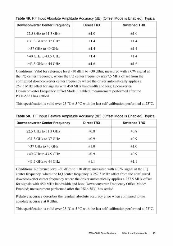
Table 49. RF Input Absolute Amplitude Accuracy (dB) (Offset Mode is Enabled), Typical
Downconverter Center Frequency Direct TRX Switched TRX
22.5 GHz to 31.3 GHz ±1.0 ±1.0
>31.3 GHz to 37 GHz ±1.4 ±1.4
>37 GHz to 40 GHz ±1.4 ±1.4
>40 GHz to 43.5 GHz ±1.4 ±1.4
>43.5 GHz to 44 GHz ±1.6 ±1.6
Conditions: Valid for reference level -30 dBm to +30 dBm; measured with a CW signal atthe I/Q center frequency, where the I/Q center frequency is257.5 MHz offset from theconfigured downconverter center frequency where the driver automatically applies a257.5 MHz offset for signals with 450 MHz bandwidth and less; Upconverter/Downconverter Frequency Offset Mode: Enabled; measurement performed after thePXIe-5831 has settled.
This specification is valid over 23 °C ± 5 °C with the last self-calibration performed at 23°C.
Table 50. RF Input Relative Amplitude Accuracy (dB) (Offset Mode is Enabled), Typical
Downconverter Center Frequency Direct TRX Switched TRX
22.5 GHz to 31.3 GHz ±0.8 ±0.8
>31.3 GHz to 37 GHz ±0.9 ±0.9
>37 GHz to 40 GHz ±1.0 ±1.0
>40 GHz to 43.5 GHz ±0.9 ±0.9
>43.5 GHz to 44 GHz ±1.1 ±1.1
Conditions: Reference level -30 dBm to +30 dBm; measured with a CW signal at the I/Qcenter frequency, where the I/Q center frequency is 257.5 MHz offset from the configureddownconverter center frequency where the driver automatically applies a 257.5 MHz offsetfor signals with 450 MHz bandwidth and less; Downconverter Frequency Offset Mode:Enabled; measurement performed after the PXIe-5831 has settled.
Relative accuracy describes the residual absolute accuracy error when compared to theabsolute accuracy at 0 dBm.
This specification is valid over 23 °C ± 5 °C with the last self-calibration performed at 23°C.
PXIe-5831 Specifications | © National Instruments | 45

RF Input Frequency Response
Table 51. TRX RF Input Frequency Response (dB)
Downconverter CenterFrequency Specification21 Typical-9522 Typical22
22.5 GHz to 31.3 GHz 2.1 1.5 1.2
>31.3 GHz to 37 GHz 2.1 1.3 1.1
>37 GHz to 40 GHz 2.1 1.4 1.3
>40 GHz to 44 GHz 2.9 1.8 1.6
Conditions: Valid over 23 °C ± 5 °C with self-calibration at 23 °C; for Direct and SwitchedTRX ports; input reference level -30 dBm to 0 dBm for specification; -30 dBm to 30 dBmfor typical.
Frequency response is defined as the maximum relative amplitude deviation from thereference offset frequency over the instantanous bandwidth. For the PXIe-5831 RF input, thereference offset frequency is 10 MHz higher than the downconverter center frequency. Forthe absolute amplitude accuracy at the reference offset, refer to the RF Input AmplitudeAccuracy section.
Figure 22. RF Input Frequency Response, 0 dBm, Reference Level, Equalized,Measured at Direct TRX Port
1
–0.8
–0.4
0.4
0.8
500–1
–500Frequency Offset (MHz)
Am
plitu
de (
dB)
0
–0.6
–0.2
0.6
0.2
–300 –100 400100–400 –200 200 3000
22.5 GHz28 GHz39 GHz43.5 GHz
46 | ni.com | PXIe-5831 Specifications

Figure 23. Maximum RF Input Frequency Response Deviation Versus DownconverterCenter Frequency, Measured at Direct TRX Port
1.5
0.2
0.3
0.4
0.5
0.6
0.8
1.2
1.4
450.1
22.5Downconverter Center Frequency (GHz)
Max
imum
Fre
quen
cy R
espo
nse
Dev
iatio
n (d
B)
1
0.7
0.9
1.3
1.1
27.5 32.5 42.537.5
30 dBm0 dBm–30 dBm
25 30 4035
Figure 24. Maximum RF Input Frequency Response Deviation versus DownconverterCenter Frequency, Measured at Switched Port
1.5
0.25
0.5
0.75
1
1.25
44420
22
Downconverter Center Frequency (GHz)
Max
imum
Fre
quen
cy R
espo
nse
Dev
iatio
n (d
B)
26 30 3834 4024 28 3632
–30 dBm
Reference Level:30 dBm0 dBm
PXIe-5831 Specifications | © National Instruments | 47

RF Input Average Noise Density
Table 52. RF Input Average Noise Density (dBm/Hz), Typical
Downconverter CenterFrequency
-30 dBm Reference Level 0 dBm Reference Level
Direct TRXPorts
Switched TRXPorts
Direct TRXPorts
Switched TRXPorts
22.5 GHz to 31.3 GHz -161 -156 -137 -136
>31.3 GHz to 37 GHz -163 -158 -141 -139
>37 GHz to 40 GHz -162 -157 -139 -139
>40 GHz to 44 GHz -160 -155 -139 -138
Conditions: Input terminated with a 50 Ω load; 30 averages; 40 dB baseband signalattenuation; noise measurement frequency offset by 6 MHz from the downconverter centerfrequency.
RF Input Third-Order Intermodulation
Table 53. Direct RF Input Third-Order Intercept Point (IIP3) (dBm), Typical
Downconverter CenterFrequency
Reference Level
-30 dBm 0 dBm 15 dBm
22.5 GHz to 31.3 GHz -15 15 28
>31.3 GHz to 37 GHz -21 10 26
>37 GHz to 40 GHz -23 9 25
>40 GHz to 44 GHz -20 10 26
Conditions: Measured by generating two -6 dBr tones centered at +95 MHz and +105 MHzoffset from the downconverter center frequency.
Table 54. Switched RF Input Third-Order Intercept Point (IIP3) (dBm), Typical
Downconverter CenterFrequency
Reference Level
-30 dBm 0 dBm 15 dBm
22.5 GHz to 31.3 GHz -18 13 26
>31.3 GHz to 37 GHz -17 10 26
48 | ni.com | PXIe-5831 Specifications
Table 54. Switched RF Input Third-Order Intercept Point (IIP3) (dBm),Typical (Continued)
Downconverter CenterFrequency
Reference Level
-30 dBm 0 dBm 15 dBm
>37 GHz to 40 GHz -18 9 24
>40 GHz to 44 GHz -23 8 25
Conditions: Measured by generating two -6 dBr tones centered at +95 MHz and +105 MHzoffset from the downconverter center frequency.
RF Input Residual Spurs
Table 55. RF Input Residual Spurs (dBm), Typical
Frequency Direct TRX Port Switched TRX Port
22.5 GHz to 31.3 GHz -74 -78
>31.3 GHz to 37 GHz -75 -72
>37 GHz to 40 GHz -73 -72
>40 GHz to 44 GHz -78 -79
Conditions: Reference level 0 dBm. Measured with the TRX ports terminated with 50 Ω.
RF Input LO Residual Power
Table 56. RF Direct and Switched TRX Input LO Residual Power (dBr23), Typical
Downconverter CenterFrequency
Self-Calibration °C ± 1 °C Self-Calibration °C ± 5 °C
22.5 GHz to 31.3 GHz -52 -40
>31.3 GHz to 37 GHz -52 -40
>37 GHz to 40 GHz -52 -40
23 dBr is relative to the full scale of the configured RF reference level.
PXIe-5831 Specifications | © National Instruments | 49
Table 56. RF Direct and Switched TRX Input LO Residual Power (dBr23),Typical (Continued)
Downconverter CenterFrequency
Self-Calibration °C ± 1 °C Self-Calibration °C ± 5 °C
>40 GHz to 44 GHz -53 -40
Conditions: Reference level is -30 dBm to +15 dBm. Input tone power at a maximum of-3 dBr. LO1 and LO2 LO Source property set to Onboard.
Figure 25. RF Input LO Residual Power, Measured
0
–80
–30
–10
44–100
22Downconverter Center Frequency (GHz)
Res
idua
l LO
Pow
er (
dBr)
–50
–60
–20
–40
26 30 4224 28 38
–90
–70
32 34 4036
30 dBm Reference Level0 dBm Reference Level–30 dBm Reference Level
RF Input Residual Sideband Image
Table 57. RF Direct and Switched TRX Input Residual Sideband Image (dBc), Typical
Downconverter CenterFrequency
Self-Calibration °C ± 1 °C Self-Calibration °C ± 5 °C
22.5 GHz to 31.3 GHz -53 -43
>31.3 GHz to 37 GHz -60 -54
>37 GHz to 40 GHz -60 -53
23 dBr is relative to the full scale of the configured RF reference level.
50 | ni.com | PXIe-5831 Specifications

Table 57. RF Direct and Switched TRX Input Residual Sideband Image (dBc),Typical (Continued)
Downconverter CenterFrequency
Self-Calibration °C ± 1 °C Self-Calibration °C ± 5 °C
>40 GHz to 44 GHz -55 -45
Conditions: Peak input power levels -30 dBm to +15 dBm. LO1 and LO2 LO Sourceproperty set to Onboard.
This specification describes the maximum residual sideband image within the 1 GHz deviceinstantaneous bandwidth.
Figure 26. RF Input Residual Sideband Image, 0 dBm, Input Power Level, Measured atDirect TRX Port
0
–60
–20
500–100
–500Frequency Offset (MHz)
Res
idua
l Im
age
(dB
c)
–40
–80
–300 –100 400100–400 –200 200 3000
22.5 GHz28 GHz39 GHz43.5 GHz
PXIe-5831 Specifications | © National Instruments | 51
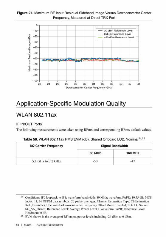
Figure 27. Maximum RF Input Residual Sideband Image Versus Downconverter CenterFrequency, Measured at Direct TRX Port
0
–80
–30
–10
44–100
22Downconverter Center Frequency (GHz)
Max
imum
Res
idua
l Im
age
(dB
c)
–50
–60
–20
–40
26 30 4224 28 38
–90
–70
32 34 4036
30 dBm Reference Level0 dBm Reference Level–30 dBm Reference Level
Application-Specific Modulation Quality
WLAN 802.11ax
IF IN/OUT Ports
The following measurements were taken using RFmx and corresponding RFmx default values.
Table 58. WLAN 802.11ax RMS EVM (dB), Shared Onboard LO2, Nominal24,25
I/Q Carrier Frequency Signal Bandwidth
80 MHz 160 MHz
5.1 GHz to 7.2 GHz -50 -47
24 Conditions: IF0 loopback to IF1; waveform bandwidth: 80 MHz; waveform PAPR: 10.55 dB; MCSIndex: 11; 16 OFDM data symbols; 20 packet averages; Channel Estimation Type: Ch EstimationRef (Preamble); Upconverter/Downconverter Frequency Offset Mode: Enabled; LO2 LO Source:SG_SA_Shared; Reference Level: Average Power Level + Waveform PAPR; Reference LevelHeadroom: 0 dB.
25 EVM shown is the average of RF output power levels including -24 dBm to 0 dBm.
52 | ni.com | PXIe-5831 Specifications

Figure 28. WLAN 802.11ax RMS EVM versus Average Power, Measured24
–40
–50
–48
–44
–42
–41
10–52
–40Measured Average Power (dBm)
EV
M (
dB)
–46
–51
–49
–47
–43
–45
–36 –8–32 –28 –24 –20 –16 –12 –4 0 4 8
5.2 GHz6.5 GHz7.2 GHz
Figure 29. WLAN 802.11ax RMS EVM versus Frequency, Nominal24,25
–48
–50
–49
–48.5
86–52
5
Frequency (GHz)
EV
M (
dB)
–51
–51.5
–49.5
–50.5
5.2 5.6 6.46.25.4 5.8 6.6 6.8 7 7.2 7.4 7.6 7.8
PXIe-5831 Specifications | © National Instruments | 53
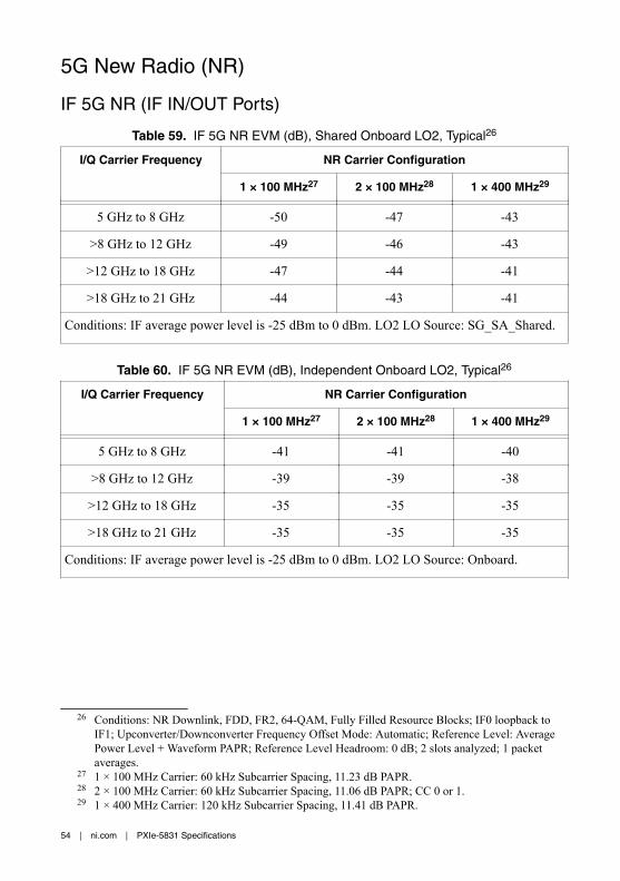
5G New Radio (NR)
IF 5G NR (IF IN/OUT Ports)
Table 59. IF 5G NR EVM (dB), Shared Onboard LO2, Typical26
I/Q Carrier Frequency NR Carrier Configuration
1 × 100 MHz27 2 × 100 MHz28 1 × 400 MHz29
5 GHz to 8 GHz -50 -47 -43
>8 GHz to 12 GHz -49 -46 -43
>12 GHz to 18 GHz -47 -44 -41
>18 GHz to 21 GHz -44 -43 -41
Conditions: IF average power level is -25 dBm to 0 dBm. LO2 LO Source: SG_SA_Shared.
Table 60. IF 5G NR EVM (dB), Independent Onboard LO2, Typical26
I/Q Carrier Frequency NR Carrier Configuration
1 × 100 MHz27 2 × 100 MHz28 1 × 400 MHz29
5 GHz to 8 GHz -41 -41 -40
>8 GHz to 12 GHz -39 -39 -38
>12 GHz to 18 GHz -35 -35 -35
>18 GHz to 21 GHz -35 -35 -35
Conditions: IF average power level is -25 dBm to 0 dBm. LO2 LO Source: Onboard.
26 Conditions: NR Downlink, FDD, FR2, 64-QAM, Fully Filled Resource Blocks; IF0 loopback toIF1; Upconverter/Downconverter Frequency Offset Mode: Automatic; Reference Level: AveragePower Level + Waveform PAPR; Reference Level Headroom: 0 dB; 2 slots analyzed; 1 packetaverages.
27 1 × 100 MHz Carrier: 60 kHz Subcarrier Spacing, 11.23 dB PAPR.28 2 × 100 MHz Carrier: 60 kHz Subcarrier Spacing, 11.06 dB PAPR; CC 0 or 1.29 1 × 400 MHz Carrier: 120 kHz Subcarrier Spacing, 11.41 dB PAPR.
54 | ni.com | PXIe-5831 Specifications

Figure 30. IF 5G NR 1 CC x 100 MHz RMS EVM versus Average Power, Measured26,27
–20
–45
–35
–25
5–20–55
–45Average Power (dBm)
RM
S E
VM
(dB
)
–40
–30
–50
–40 –35 –30 –25 –10–15 –5 0
5.5 GHz (Shared LO2)10 GHz (Shared LO2)18 GHz (Shared LO2)5.5 GHz (Independent LO2)10 GHz (Independent LO2)18 GHz (Independent LO2)
Figure 31. IF 5G NR 2 CC x 100 MHz RMS EVM versus Average Power, Measured26,28
–20
–45
–35
–25
5–20–55
–45Average Power (dBm)
RM
S E
VM
(dB
)
–40
–30
–50
–40 –35 –30 –25 –10–15 –5 0
5.5 GHz (Shared LO2)10 GHz (Shared LO2)18 GHz (Shared LO2)5.5 GHz (Independent LO2)10 GHz (Independent LO2)18 GHz (Independent LO2)
PXIe-5831 Specifications | © National Instruments | 55

Figure 32. IF 5G NR 1 CC x 400 MHz RMS EVM versus Average Power, Measured26,29
–20
–45
–35
–25
5–20–55
–45Average Power (dBm)
RM
S E
VM
(dB
)
–40
–30
–50
–40 –35 –30 –25 –10–15 –5 0
5.5 GHz (Shared LO2)10 GHz (Shared LO2)18 GHz (Shared LO2)5.5 GHz (Independent LO2)10 GHz (Independent LO2)18 GHz (Independent LO2)
Figure 33. IF 5G NR 2 CC x 400 MHz RMS EVM versus Average Power, Measured26,30
–20
–45
–35
–25
5–20–55
–45Average Power (dBm)
RM
S E
VM
(dB
)
–40
–30
–50
–40 –35 –30 –25 –10–15 –5 0
5.5 GHz (Shared LO2)10 GHz (Shared LO2)18 GHz (Shared LO2)5.5 GHz (Independent LO2)10 GHz (Independent LO2)18 GHz (Independent LO2)
30 2 × 400 MHz Carriers: 120 kHz Subcarrier Spacing, 11.88 dB PAPR; CC 0.
56 | ni.com | PXIe-5831 Specifications

Figure 34. IF 5G NR RMS EVM versus Frequency (Shared LO2), Measured26,31,32
–20
–45
–35
–25
2114–55
5Center Frequency (GHz)
RM
S E
VM
(dB
)
–40
–30
–50
6 8 10 12 157 9 11 13 1716 18 19 20
1 CC x 100 MHz 2 CC x 100 MHz 1 CC x 400 MHz 2 CC x 400 MHz
Figure 35. IF 5G NR RMS EVM versus Frequency (Independent LO2), Measured26,31,32
–20
–45
–35
–25
2114–55
5Center Frequency (GHz)
RM
S E
VM
(dB
)
–40
–30
–50
6 8 10 12 157 9 11 13 1716 18 19 20
1 CC x 100 MHz 2 CC x 100 MHz 1 CC x 400 MHz 2 CC x 400 MHz
31 1 × 100 MHz Carrier: 60 kHz Subcarrier Spacing, 11.23 dB PAPR. 2 × 100 MHz Carrier: 60 kHzSubcarrier Spacing, 11.06 dB PAPR; CC 0. 1 × 400 MHz Carrier: 120 kHz Subcarrier Spacing,11.41 dB PAPR. 2 × 400 MHz Carriers: 120 kHz Subcarrier Spacing, 11.88 dB PAPR; CC 0.
32 IF output average power level is -10 dBm.
PXIe-5831 Specifications | © National Instruments | 57

RF 5G NR
Table 61. Direct TRX to Direct TRX RF 5G NR EVM (dB), Nominal33'34
I/Q Carrier Frequency Shared Onboard LO2 Independent Onboard LO2
22.5 GHz to 31.3 GHz -44 -40
37 GHz to 40 GHz -43 -40
>40 GHz to 44 GHz -42 -41
Conditions: RF average power level is -10 dBm. LO1 LO Source: Onboard.
Table 62. Switched to Switched RF 5G NR EVM (dB), Nominal33'34
I/Q Carrier Frequency Shared Onboard LO2 Independent Onboard LO2
22.5 GHz to 31.3 GHz -43 -39
37 GHz to 40 GHz -43 -40
>40 GHz to 44 GHz -42 -41
Conditions: RF average power level is -10 dBm. LO1 LO Source: Onboard.
Table 63. Direct TRX to Switched or Switched to Direct TRX RF 5G NR EVM (dB),Nominal33
'34
I/Q Carrier Frequency Shared Onboard LO2 Independent Onboard LO2
22.5 GHz to 31.3 GHz -43 -39
37 GHz to 40 GHz -43 -40
>40 GHz to 44 GHz -42 -41
Conditions: RF average power level is -10 dBm. LO1 LO Source: Onboard.
33 Conditions: NR Downlink, FDD, FR2, 64-QAM, Fully Filled Resource Blocks; RF loopback toRF; Upconverter/Downconverter Frequency Offset Mode: Automatic; Reference Level: AveragePower Level + Waveform PAPR; Reference Level Headroom: 0 dB from 22.5 GHz to 31.3 GHzand 3 dB from 37 GHz to 44 GHz; LO1 LO Source: Onboard; 2 slots analyzed; 1 packet averages.
34 1 × 100 MHz Carrier: 120 kHz Subcarrier Spacing, 11.16 dB PAPR.
58 | ni.com | PXIe-5831 Specifications

Figure 36. Direct TRX to Direct TRX RF 5G NR 1 CC × 100 MHz RMS EVM versusAverage Power, Measured33
'34
–20
–40
–32
–24
5–25–50
–50Average Power (dBm)
RM
S E
VM
(dB
)
–36
–28
–44
–22
–42
–34
–26
–38
–30
–46–48
–45 –40 –35 –30 –15–20 –10 –5 0
28 GHz (Shared LO2)39 GHz (Shared LO2)28 GHz (Independent LO2)39 GHz (Independent LO2)
Figure 37. Switched to Switched RF 5G NR 1 CC x 100 MHz RMS EVM versus AveragePower, Measured33
'34
–20
–48–46
–42
–26
–22
50
–24
–28–30–32–34–36–38–40
–44
–50–50
Average Power (dBm)
RM
S E
VM
(dB
)
–40 –30 –10–20 –5–45 –35 –15–25
39 GHz (Shared LO2)
28 GHz (Shared LO2)39 GHz (Independent LO2)
28 GHz (Independent LO2)
PXIe-5831 Specifications | © National Instruments | 59

Figure 38. Switched to Direct TRX RF 5G NR 1 CC x 100 MHz RMS EVM versusAverage Power, Measured33
'34
–20
–48–46
–42
–26
–22
50
–24
–28–30–32–34–36–38–40
–44
–50–50
Average Power (dBm)
RM
S E
VM
(dB
)
–40 –30 –10–20 –5–45 –35 –15–25
39 GHz (Shared LO2)
28 GHz (Shared LO2)39 GHz (Independent LO2)
28 GHz (Independent LO2)
Figure 39. Direct TRX to Switched RF 5G NR 1 CC x 100 MHz RMS EVM versusAverage Power, Measured33
'34
–20
–48–46
–42
–26
–22
50
–24
–28–30–32–34–36–38–40
–44
–50–50
Average Power (dBm)
RM
S E
VM
(dB
)
–40 –30 –10–20 –5–45 –35 –15–25
39 GHz (Shared LO2)
28 GHz (Shared LO2)39 GHz (Independent LO2)
28 GHz (Independent LO2)
60 | ni.com | PXIe-5831 Specifications

Figure 40. Direct TRX to Direct TRX RF 5G NR RMS EVM versus Frequency,Measured33
'34
'35
–20
–46
–36
–26
–22
44–50
22Center Frequency (GHz)
RM
S E
VM
(dB
) –30
–40
–32
–24
–28
26 30 4224 28 38
–48
–38
–42
–34
–44
23 27 31 4325 29 37 4039 41
. . .
. . .
Shared LO2Independent LO2
Front Panel I/O
PXIe-5820Refer to the PXIe-5820 Specifications for more information about characteristics of thePXIe-5820 front panel input and output.
PXIe-3622I/Q IN
Connectors MMPX (female)
Input coupling, per terminal DC
Input type Differential
Number of channels 2
Differential impedance 100 Ω
I/Q OUT
Connectors MMPX (female)
Output coupling, per terminal DC
Output type Differential
35 RF average power level is -10 dBm.
PXIe-5831 Specifications | © National Instruments | 61

Number of channels 2
Impedance 100 Ω
LO1 IN and LO2 IN
Connectors MMPX (female)
Frequency range36 3.55 GHz to 7.1 GHz
Input power range37 +6 dBm to +10 dBm, nominal
Input return loss 10 dB, nominal
Absolute maximum input power +10 dBm
LO1 coupling AC coupled
LO2 coupling DC coupled to ground
Impedance 50 Ω
LO1 OUT and LO2 OUT
Connectors MMPX (female)
Frequency range 3.55 GHz to 7.1 GHz
Absolute maximum output power +10 dBm
LO1 coupling AC coupled
LO2 coupling DC coupled to ground
Output power resolution38 0.5 dB, nominal
Impedance 50 Ω
Output return loss 10 dB, nominal
DIO
Connector Mini HDMI
IF OUT mmWave
Connectors SMA 27 GHz (female)
Output impedance 50 Ω
Return loss 10 dB, nominal
Coupling AC coupled
36 This frequency range is applicable for only LO2 IN when using the PXIe-5831 IF and mmWaveinstrument configuration.
37 The PXIe-5831 supports receiving an external LO with a range of signal power levels. To properlyconfigure the PXIe-5831 LO signal path for the provided level, set NIRFSA_ATTR_LO_IN_POWERor NIRFSG_ATTR_LO_IN_POWER.
38 Output power resolution refers to the RF attenuator step size used to compensate for the LO outputpower.
62 | ni.com | PXIe-5831 Specifications

IF IN mmWave
Connectors SMA 27 GHz (female)
Input impedance 50 Ω
Return loss 10 dB, nominal
Coupling AC coupled
IF IN/OUT
Connectors SMA 27 GHz (female)
Impedance 50 Ω
Coupling AC coupled
Absolute maximum input power +25 dBm
Absolute maximum reverse power Not to exceed the active RF output powersetting
Figure 41. PXIe-3622 IF IN Port Return Loss, Measured
0
–36
–32
–28
–24
–20
–16
–8
–4–2
216 13–40
5Frequency (GHz)
Am
plitu
de (
dB)
–12
–34
–30
–26
–22
–18
–14
–6
–38
–10
7 8 9 10 11 12 14 15 16 17 18 19 20
IF IN 0IF IN 1
PXIe-5831 Specifications | © National Instruments | 63

Figure 42. PXIe-3622 IF OUT Port Return Loss, Measured
0
–36
–32
–28
–24
–20
–16
–8
–4–2
216 13–40
5Frequency (GHz)
Am
plitu
de (
dB)
–12
–34
–30
–26
–22
–18
–14
–6
–38
–10
7 8 9 10 11 12 14 15 16 17 18 19 20
IF OUT 0IF OUT 1
LO1 0 mmWave
Connector SMA 27 GHz (female)
Frequency range 3.55 GHz to 14.2 GHz
LO1 1 mmWave
Connector SMA 27 GHz (female)
Frequency range 3.55 GHz to 14.2 GHz
REF IN/OUT
Connectors MMPX (female)
Frequency 10 MHz
Input tolerance39 ±10 × 10-6
Input amplitude40 0.7 V pk-pk to 3.3 V pk-pk, typical
Coupling DC
Output amplitude 1.65 V pk-pk into 50 Ω, nominal
Impedance 50 Ω
39 Frequency Accuracy = Input Tolerance × Reference Frequency40 Jitter performance improves with increased slew rate of input signal.
64 | ni.com | PXIe-5831 Specifications

PXIe-5653
Table 64. LO Output Level
LO Minimum Nominal Maximum
LO1 (from3.2 GHz to8.2 GHz)
NominalValue -2.5 dB
Varies by frequency according to the followingequation:10.5− 3 Frequency(GHz)− 3.2GHz5.0GHz dBm
NominalValue +2.5 dB
LO1 (at8.3 GHz)
+4 dBm +6.5 dBm +9 dBm
LO2 +6.5 dBm +9 dBm +13 dBm
LO3 +7 dBm +9 dBm +13 dBm
Note The PXIe-5653 LO2 OUT and LO3 OUT connectors are not used in anyPXIe-5831 instrument configuration.
mmRH-5582DIRECT TRX PORTS
Connectors 2.4 mm (female)
Absolute maximum input power
Reference power ≤+30 dBm Reference power + 6 dB
Reference power >+30 dBm +36 dBm
Impedance 50 Ω
Absolute maximum reverse power Not to exceed the active RF output powersetting
Coupling AC
PXIe-5831 Specifications | © National Instruments | 65

Figure 43. mmRH-5582 RF Input Port Return Loss, Measured at Direct TRX Port
0
27.5
22.5
17.5
15
12.5
10
5
2.5
4432
25
20
3022
Frequency (GHz)
Ret
urn
Loss
(dB
)
7.5
24 26 3028 3836 40 423123 25 2927 3433 3937 41 4335
Figure 44. mmRH-5582 RF Output Port Return Loss, Measured at Direct TRX Port
0
27.5
22.5
17.5
15
12.5
10
5
2.5
44. . .
25
20
3022
Frequency (GHz)
Ret
urn
Loss
(dB
)
7.5
24 26 3028 38 40 423123 25 2927 3937 41 43
66 | ni.com | PXIe-5831 Specifications

Figure 45. mmRH-5582 RF Input Port Return Loss, Measured at Switched TRX Port
0
–35
–30
–20
–10
4442
–5
–15
–25
–4022
Frequency (GHz)
Ret
urn
Loss
(dB
)
26 30 3834 4024 28 3632
Figure 46. mmRH-5582 RF Output Port Return Loss, Measured at Switched TRX Port
0
–35
–30
–20
–10
4442
–5
–15
–25
–4022
Frequency (GHz)
Ret
urn
Loss
(dB
)
26 30 3834 4024 28 3632
SWITCHED TRX PORTS
Connectors 2.4 mm (female)
Absolute maximum input power
Reference power ≤+30 dBm Reference power + 6 dB
Reference power >+30 dBm +36 dBm
Impedance 50 Ω
PXIe-5831 Specifications | © National Instruments | 67

Absolute maximum reverse power Not to exceed the active RF output powersetting
Coupling AC
IF OUT
Connector SMA 27 GHz (female)
Impedance 50 Ω
LO IN
Connector SMA 27 GHz (female)
Frequency range 10 GHz to 13.5 GHz
Input power +5 dBm, nominal
Impedance 50 Ω, nominal
Absolute maximum input power +20 dBm
Coupling DC
IF IN
Connector SMA 27 GHz (female)
Impedance 50 Ω, nominal
Absolute maximum input power +10 dBm
Coupling AC
DIO IN
Connector Mini HDMI
DIO OUT
Connector Mini HDMI
Power Requirements
Table 65. PXIe-5831 Power Requirements, Nominal
Module +3.3 VDC +12 VDC Total Power (W)
PXIe-5820 3.3 A (10.89 W) 6.0 A (72.0 W) 82.89
PXIe-3622 5.0 A (6.93 W) 5.0 A (67.2 W) 74.13
PXIe-5653 1.10 A (3.63 W) 4.0 A (48.0 W) 51.63
PXIe-5831 (combined instrument) — — 208.65
68 | ni.com | PXIe-5831 Specifications

Table 66. mmRH-5582 Power Requirements
Module +12 VDC Total Power (W)
mmRH-5582 (Direct TRX Ports Only) 3.8 A 45.6
mmRH-5582 (Switched and Direct TRX Ports) 4.1 A 49.2
mmRH-5582 (Switched TRX Ports Only) 4.4 A 52.8
CalibrationInterval 1 year
Physical Characteristics
Table 67. PXIe-5831 Physical Characteristics, Nominal
Module Dimensions Weight
Grams Ounces
PXIe-5820 3U, 2 slots 795 28.0
PXIe-3622 3U, 2 slots 1,066 37.6
PXIe-5653 3U, 2 slots 1,076 37.8
PXIe-5831 (combined instrument) 3U, 6 slots 2,937 103.4
Table 68. mmRH-5582 Physical Characteristics, Nominal
Module Dimensions Weight
Grams Ounces
mmRH-5582 (Direct TRXPorts Only)
21.9 cm × 15.5 cm × 9.9 cm(8.65 in. × 6.11 in. × 3.91 in.)
2,940 103.7
mmRH-5582 (Switched andDirect TRX Ports)
3,132 110.5
mmRH-5582 (Switched TRXPorts Only)
3,324 117.3
PXIe-5831 Specifications | © National Instruments | 69

Environmental CharacteristicsTemperature and Humidity
Temperature
Operating 0 °C to 45 °C
Storage -41 °C to 71 °C
Humidity
Operating 10% to 90%, noncondensing
Storage 5% to 95%, noncondensing
Pollution Degree 2
Maximum altitude 2,000 m (800 mbar) (at 25 °C ambient temperature)
Shock and Vibration
Random vibration
Operating 5 Hz to 500 Hz, 0.3 g RMS
Non-operating 5 Hz to 500 Hz, 2.4 g RMS
Operating shock 30 g, half-sine, 11 ms pulse
Environmental ManagementNI is committed to designing and manufacturing products in an environmentally responsiblemanner. NI recognizes that eliminating certain hazardous substances from our products isbeneficial to the environment and to NI customers.
For additional environmental information, refer to the Commitment to the Environment webpage at ni.com/environment. This page contains the environmental regulations and directiveswith which NI complies, as well as other environmental information not included in thisdocument.
Waste Electrical and Electronic Equipment (WEEE)EU Customers At the end of the product life cycle, all NI products must bedisposed of according to local laws and regulations. For more information abouthow to recycle NI products in your region, visit ni.com/environment/weee.
电子信息产品污染控制管理办法(中国 RoHS)中国客户 National Instruments 符合中国电子信息产品中限制使用某些有害物
质指令(RoHS)。关于 National Instruments 中国 RoHS 合规性信息,请登录
ni.com/environment/rohs_china。(For information about China RoHScompliance, go to ni.com/environment/rohs_china.)
70 | ni.com | PXIe-5831 Specifications

Appendix A: PXIe-5653 LO1 Single SidebandPhase Noise
Figure 47. PXIe-5653 Phase Noise, Measured41 (Spurs Not Shown)
Offset (Hz)
Pha
se N
oise
(dB
c/H
z)
10–160
–130
–140
–120
–110
–100
–90
–80
–40
–50
–60
–70
–30
–150
100 1 k 10 k 100 k 1 M 10 M
41 LO1 frequency is 5 GHz. Representative of nominal performance difference across the entirefrequency range of LO1.
PXIe-5831 Specifications | © National Instruments | 71

Appendix B: PXIe-3622 Single Sideband PhaseNoiseFigure 48. PXIe-3622 Internal LO1 VCO Phase Noise, Measured42 (Spurs Not Shown)
–50
–150
–140
–130
–120
–110
–100
–80
–70
–60
100 M100 1 k 10 k 100 k 1 M 10 M–160
10Frequency Offset (Hz)
Pha
se N
oise
(dB
c/H
z)
–90
3.55 GHz7.1 GHz
42 Measured at the PXIe-3622 LO1 OUT port.
Information is subject to change without notice. Refer to the NI Trademarks and Logo Guidelines at ni.com/trademarks forinformation on NI trademarks. Other product and company names mentioned herein are trademarks or trade names of theirrespective companies. For patents covering NI products/technology, refer to the appropriate location: Help»Patents in yoursoftware, the patents.txt file on your media, or the National Instruments Patent Notice at ni.com/patents. You can findinformation about end-user license agreements (EULAs) and third-party legal notices in the readme file for your NI product. Referto the Export Compliance Information at ni.com/legal/export-compliance for the NI global trade compliance policy and howto obtain relevant HTS codes, ECCNs, and other import/export data. NI MAKES NO EXPRESS OR IMPLIED WARRANTIES ASTO THE ACCURACY OF THE INFORMATION CONTAINED HEREIN AND SHALL NOT BE LIABLE FOR ANY ERRORS. U.S.Government Customers: The data contained in this manual was developed at private expense and is subject to the applicablelimited rights and restricted data rights as set forth in FAR 52.227-14, DFAR 252.227-7014, and DFAR 252.227-7015.
© 2019—2020 National Instruments. All rights reserved.
377805B-01 March 12, 2020
Related Documents