Pulse Circuit Applications By SAM WILSON, CET 80705-3

Welcome message from author
This document is posted to help you gain knowledge. Please leave a comment to let me know what you think about it! Share it to your friends and learn new things together.
Transcript
Pulse Circuit Applications
By
SAM WILSON, CET
80705-3
Edition 1
Pulse Circuit Applications Instructional Objectives
In the previous lesson, you learned about timers, especially IC (integrated-circuit) timers, and you looked at a few applications.
In this lesson, you'll add to your knowledge of such timers. Modifications of the basic timing circuit will be discussed first; then you 'lllearn how the 555 timer can be used in various other applications. Remember that the output of a timer is a pulse and this pulse may be used for additional switching applications. Pulses are also used for regulating power supplies, switching networks, and operating computers.
Among the most important functions in industrial electronics are testing and measuring; so we've included some examples of digital measuring equipment in this lesson to give you an idea of what this equipment can do.
to: After you have studied this lesson, you should be able
• Determine the on period for a 555 monostable multivibrator circuit.
• Describe how a 555 timer can be used in an astable multivibrator circuit.
• Determine the free-running frequency of a 555 astable multivibrator.
• Discuss the use of synchronization for astable multivibrators, and for astable 555 timer freerunning circuits.
• Describe how pulses are used for measuring both voltage and capacity, and how switching regulators work in power-supply systems.
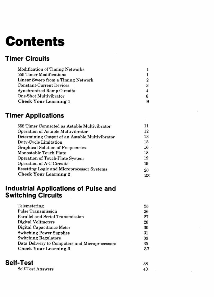
Contents Timer Circuits
Modification of Timing Networks 555 Timer Modifications Linear Sweep from a Timing Network Constant-Current Devices Synchronized Ramp Circuits One-Shot Multivibrator Check Your Learning 1
Timer Applications
555 Timer Connected as Astable Multivibrator Operation of Astable Multivibrator Determining Output of an Astable Multivibrator Duty-Cycle Limitation Graphical Solution of Frequencies Monostable Touch Plate Operation of Touch-Plate System Operation of A-C Circuits Resetting Logic and Microprocessor Systems Check Your Learning 2
Industrial Applications of Pulse and Switching Circuits
Telemetering Pulse Transmission Parallel and Serial Transmission Digital Voltmeters Digital Capacitance Meter Switching Power Supplies Switching Regulators Data Delivery to Computers and Microprocessors Check Your Learning 3
Self-Test Self-Test Answers
1 1 2 3 4 6 9
11 12 13 15 16 18 19 19
20 23
25 26 27 28 30 31 33 35 37
38 40
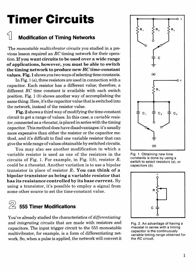
Timer Circuits Modification of Timing Networks
The monostable multivibrator circuits you studied in a previous lesson required an RC timing network for their operation. If you want circuits to be used over a wide range of applications, however, you must be able to switch the timing network to produce new RC time-constant values. Fig. 1 shows you two ways of selecting time constants.
In Fig. 1 (a), three resistors are used in connection with a capacitor. Each resistor has a different value; therefore, a different RC time constant is available with each switch position. Fig. 1 (b) shows another way of accomplishing the same thing. Here, it's the capacitor value that is switched into the network, instead of the resistor value.
Fig. 2 shows a third way of modifying the time-constant circuit to get a range of values. In this case, a variable resistor, connected as a rheostat, is placed in series with the timing capacitor. This method does have disadvantages: it's usually more expensive than either the resistor or the capacitor method, and it's difficult to find one variable resistor that can give the wide range of values obtainable by switched circuits.
You may also see another modification in which a variable resistor is used as one of the resistors in the circuits of Fig. 1. For example, in Fig. l(b), resistor R1 could be a rheostat. Another variation is to use a bipolar transistor in place of resistor R 1. You can think of a bipolar transistor as being a variable resistor that has its resistance controlled by its base current. By using a transistor, it's possible to employ a signal from some other source to set the time-constant value.
~ 555 Timer Modifications
You've already studied the characteristics of differentiating and integrating circuits that are made with resistors and capacitors. The input trigger circuit to the 555 monostable multivibrator, for example, is a form of differentiating network. So, when a pulse is applied, the network will convert it
t----+--...... --o+
(a)
r-------o+
R,
(b)
Fig. 1. Obtaining new time constants is done by using a switch to select resistors (a), or capacitors (b).
+
Fig. 2. An advantage of having a rheostat in series with a timing capacitor is the continuously variable timing range obtained for the RC circuit.
1
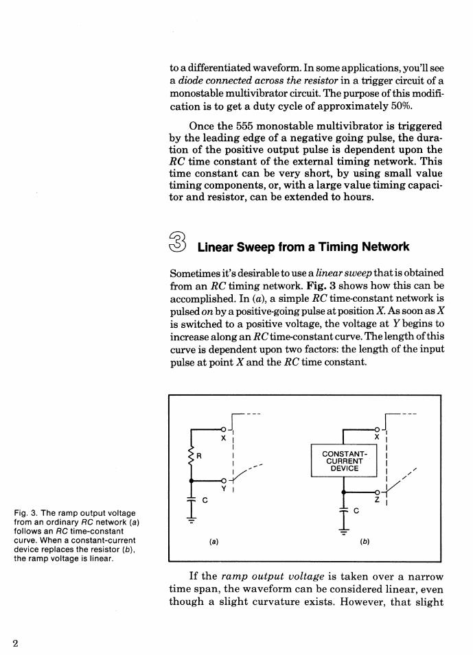
Fig. 3. The ramp output voltage from an ordinary RC network (a) follows an RC time-constant curve. When a constant-current device replaces the resistor (b), the ramp voltage is linear.
2
to a differentiated waveform. In some applications, you'll see a diode connected across the resistor in a trigger circuit of a monostable multivibrator circuit. The purpose of this modification is to get a duty cycle of approximately 50%.
Once the 555 monostable multivibrator is triggered by the leading edge of a negative going pulse, the duration of the positive output pulse is dependent upon the RC time constant of the external timing network. This time constant can be very short, by using small value timing components, or, with a large value timing capacitor and resistor, can be extended to hours.
Linear Sweep from a Timing Network
Sometimes it's desirable to use a linear sweep that is obtained from an RC timing network. Fig. 3 shows how this can be accomplished. In (a), a simple RC time-constant network is pulsed on by a positive-going pulse at position X. As soon as X is switched to a positive voltage, the voltage at Y begins to increase along an RCtime-constant curve. The length of this curve is dependent upon two factors: the length of the input pulse at point X and the RC time constant.
..--oJ __ _ X :
I I I ~' ...,_--o-V,
y I
(a)
,----oJ __ _ X I
.-------L---, I I
CONSTANTCURRENT
DEVICE
I I I /" I /
.--~-V Z I
(b)
If the ramp output voltage is taken over a narrow time span, the waveform can be considered linear, even though a slight curvature exists. However, that slight
curvature may not be acceptable in some applications, so the circuit may be modified as shown in (b). Here, a constant-current device is connected in place of the resistor. (A constant-current device has the same amount of current flowing through it, even though the voltage across it may change.) Note that the ramp voltage at Z is linear, since the charging current in the capacitor is a constant value.
~ Constant-Current Devices
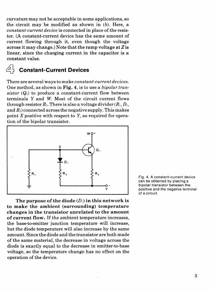
There are several ways to make constant-current devices. One method, as shown in Fig. 4, is to use a bipolar transistor (QI) to produce a constant-current flow between terminals Y and W. Most of the circuit current flows through resistor R3. There is also a voltage divider (R1, D1, and R2) connected across the negative supply. This makes point X positive with respect to Y, as required for operation of the bipolar transistor.
X
y
The purpose of the diode (D1) in this network is to make the ambient (surrounding) temperature changes in the transistor unrelated to the amount of current flow. If the ambient temperature increases, the base-to-emitter junction temperature will increase, but the diode temperature will also increase by the same amount. Since the diode and the transistor are both made of the same material, the decrease in voltage across the diode is exactly equal to the decrease in emitter-to-base voltage, so the temperature change has no effect on the operation of the device.
Fig. 4. A constant-current device can be obtained by placing a bipolar transistor between the positive and the negative terminal of a circuit.
3
+
(a) (b)
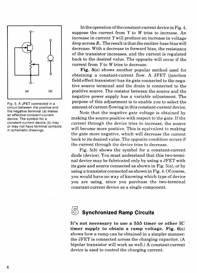
Fig. 5. A JFET connected in a circuit between the positive and the negative terminal (a) makes an effective constant-current device. The symbol for a constant-current device (b) may or may not have terminal symbols in schematic drawings.
4
In the operation of the cons tan t-curren t device in Fig. 4, suppose the current from Y to W tries to increase. An increase in current Y will produce an increase in voltage drop across R3. The result is that the emitter-base bias will decrease. With a decrease in forward bias, the resistance of the transistor increases, and the current is regulated back to the desired value. The opposite will occur if the current from Y to W tries to decrease.
Fig. 5(a) shows another popular method used for obtaining a constant-current flow. A JFET (junction field-effect transistor) has its gate connected to the negative source terminal and the drain is connected to the positive source. The resistor between the source and the negative power supply has a variable adjustment. The purpose of this adjustment is to enable you to select the amount of current flowing in this constant-current device.
Note that the negative gate voltage is obtained by making the source positive with respect to the gate. If the current through the device tries to increase, the source will become more positive. This is equivalent to making the gate more negative, which will decrease the current back to its desired value. The opposite condition occurs if the current through the device tries to decrease.
Fig. 5(b) shows the symbol for a constant-current diode (device). You must understand that this two-terminal device may be fabricated only by using a JFET with its gate and source connected as shown in Fig. 5(a), or by using a transistor connected as shown in Fig. 4. Of course, you would have no way of knowing which type of device you are using, since you purchase the two-terminal constant-current device as a single component.
@ Synchronized Ramp Circuits
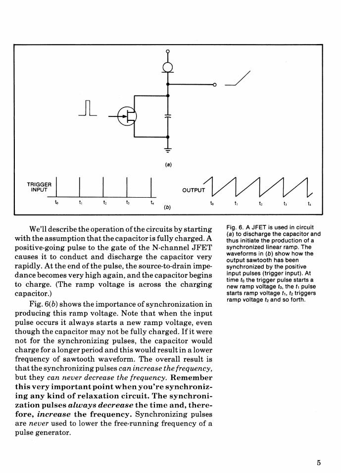
It's not necessary to use a 555 timer or other IC timer supply to obtain a ramp voltage. Fig. 6(a) shows how a ramp can be obtained in a simpler manner: the JFET is connected across the charging capacitor. (A bipolar transistor will work as well.) A constant-current device is used to control the charging current.
JL
':'"
(a)
TRIGGER I INPUT
to tl t2 t3 t. to (b)
We'll describe the operation of the circuits by starting with the assumption that the capacitor is fully charged. A positive-going pulse to the gate of theN-channel JFET causes it to conduct and discharge the capacitor very rapidly. At the end of the pulse, the source-to-drain impedance becomes very high again, and the capacitor begins to charge. (The ramp voltage is across the charging capacitor.)
Fig. 6(b) shows the importance of synchronization in producing this ramp voltage. Note that when the input pulse occurs it always starts a new ramp voltage, even though the capacitor may not be fully charged. If it were not for the synchronizing pulses, the capacitor would charge for a longer period and this would result in a lower frequency of sawtooth waveform. The overall result is that the synchronizing pulses can increase the frequency, but they can never decrease the frequency. Remember this very important point when you're synchronizing any kind of relaxation circuit. The synchronization pulses always decrease the time and, therefore, increase the frequency. Synchronizing pulses are never used to lower the free-running frequency of a pulse generator.
_/
tl t2 h t.
Fig. 6. A JFET is used in circuit (a) to discharge the capacitor and thus initiate the production of a synchronized linear ramp. The waveforms in (b) show how the output sawtooth has been synchronized by the positive input pulses (trigger input). At time to the trigger pulse starts a new ramp voltage to, the t, pulse starts ramp voltage t,, t2 triggers ramp voltage t2 and so forth.
5
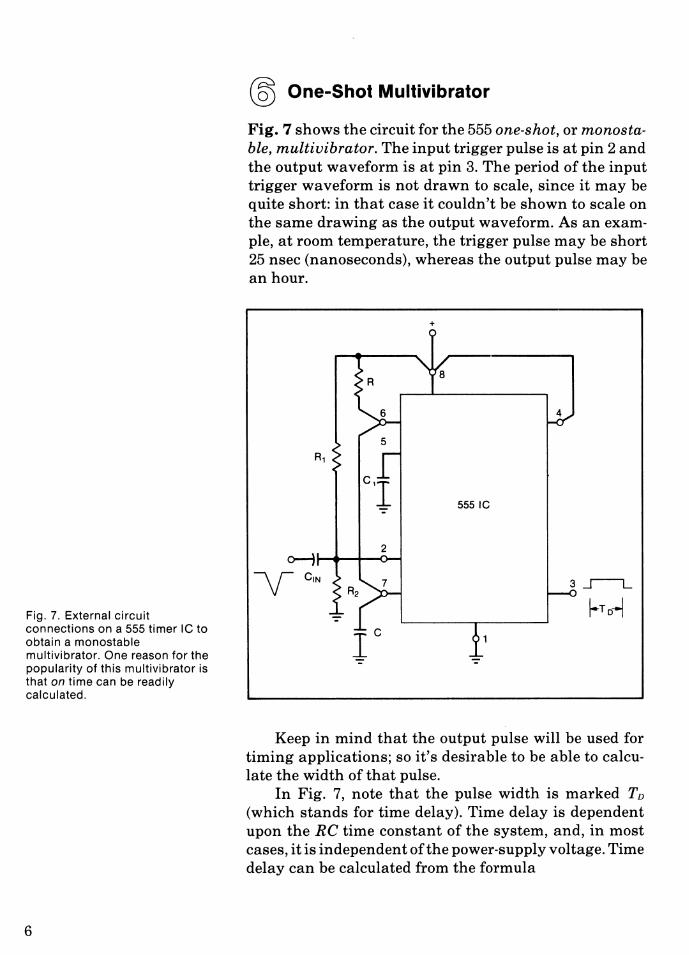
Fig. 7. External circuit connections on a 555 timer IC to obtain a monostable multivibrator. One reason for the popularity of this multivibrator is that on time can be readily calculated.
6
@ One-Shot Multivibrator
Fig. 7 shows the circuit for the 555 one-shot, or monostable, multi vibrator. The input trigger pulse is at pin 2 and the output waveform is at pin 3. The period of the input trigger waveform is not drawn to scale, since it may be quite short: in that case it couldn't be shown to scale on the same drawing as the output waveform. As an example, at room temperature, the trigger pulse may be short 25 nsec (nanoseconds), whereas the output pulse may be an hour.
+
4
5551C
2 o--; ....... -+--o-1
yciN
Keep in mind that the output pulse will be used for timing applications; so it's desirable to be able to calculate the width of that pulse.
In Fig. 7, note that the pulse width is marked TD (which stands for time delay). Time delay is dependent upon the RC time constant of the system, and, in most cases, it is independent of the power-supply voltage. Time delay can be calculated from the formula
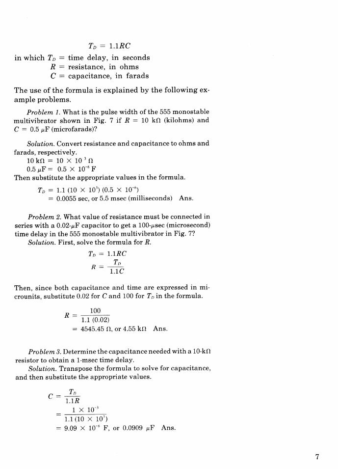
TD = l.lRC
in which TD = time delay, in seconds R = resistance, in ohms C = capacitance, in farads
The use of the formula is explained by the following example problems.
Problem 1. What is the pulse width of the 555 monostable multivibrator shown in Fig. 7 if R = 10 kn (kilohms) and C = 0.5 J.LF (microfarads)?
Solution. Convert resistance and capacitance to ohms and farads, respectively.
10 kn = 10 x 10 3 n 0.5 J.LF = 0.5 X 10⁻⁶ F
Then substitute the appropriate values in the formula.
TD = 1.1 (10 X 103) (0.5 X 10"")
= 0.0055 sec, or 5.5 msec (milliseconds) Ans.
Problem 2. What value of resistance must be connected in series with a 0.02-J.LF capacitor to get a 100-J.Lsec (microsecond) time delay in the 555 monostable multi vibrator in Fig. 7?
Solution. First, solve the formula for R.
Tn = 1.1RC Tn
R = 1.1C
Then, since both capacitance and time are expressed in microunits, substitute 0.02 for C and 100 for Tn in the formula.
R = 100 1.1 (0.02)
= 4545.45 n, or 4.55 kn Ans.
Problem 3. Determine the capacitance needed with a 10-kD resistor to obtain a 1-msec time delay.
Solution. Transpose the formula to solve for capacitance, and then substitute the appropriate values.
Tn C = 1.1R
1 X 10⁻³
1.1 (10 X 103 )
= 9.09 X 10-x F, or 0.0909 J.LF Ans.
7
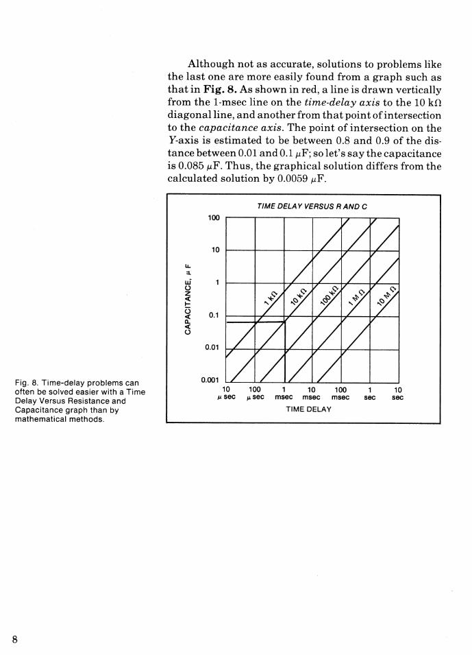
Fig. 8. Time-delay problems can often be solved easier with a Time Delay Versus Resistance and Capacitance graph than by mathematical methods.
8
Although not as accurate, solutions to problems like the last one are more easily found from a graph such as that in Fig. 8. As shown in red, a line is drawn vertically from the 1-msec line on the time-delay axis to the 10 kO diagonal line, and another from that point of intersection to the capacitance axis. The point of intersection on the Y-axis is estimated to be between 0.8 and 0.9 of the distance between 0.01 and 0.1 ,uF; so let's say the capacitance is 0.085 ,uF. Thus, the graphical solution differs from the calculated solution by 0.0059 ,uF.
LL ~
u.i () z <( 1-(3 <( a.. <( ()
TIME DELAY VERSUS RAND C
100
10
0.1
0.01
0.001 10 100 10 100
p. sec p. sec msec msec msec sec
TIME DELAY
10 sec
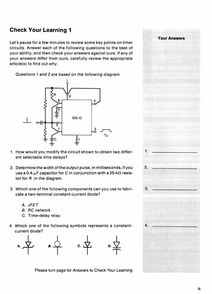
Check Your Learning 1
Let's pause for a few minutes to review some key points ~n timer circuits. Answer each of the following questions to the best of your ability, and then check your answers against ours. If any of your answers differ from ours, carefully review the appropriate article(s) to find out why.
Questions 1 and 2 are based on the following diagram. +
....r-1.... To
1. How would you modify the circuit shown to obtain two different selectable time delays?
2. Determine the width oft he output pulse, in milliseconds, if you use a 0.4-JLF capacitor for C in conjunction with a 25-kO resistor for R in the diagram.
3. Which one of the following components can you use to fabricate a two-terminal constant-current diode?
A. JFET B. RC network C. Time-delay relay
4. Which one of the following symbols represents a constantcurrent diode?
D.~ T
Please turn page for Answers to Check Your Learning
10
Answers to Check Your Learning 1
1. You can use either of the circuits shown in Fig. 1 in place of R or C.
Art. 1, Fig. 7 2. 11 msec Art. 6, Fig. 7
(To = 1.1 (25 X 103 )
(0.4 X 10⁻⁶)
= 0.011 sec = 11 msec)
3. A. JFET Art. 4
4. B. * Art. 4, Fig. 5
Timer Applications
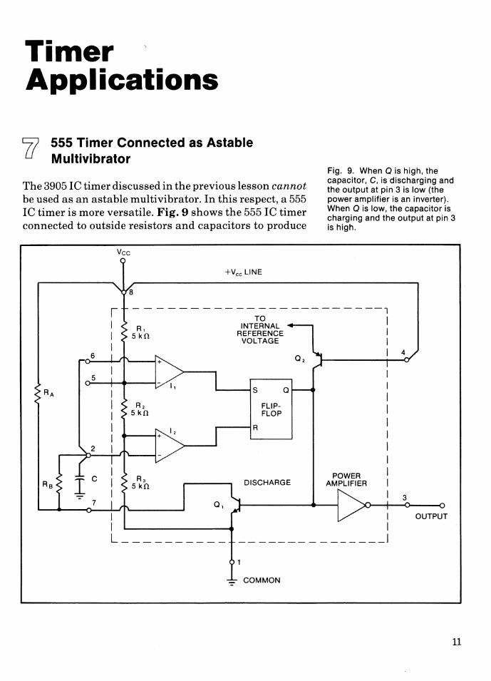
555 Timer Connected as Astable Multivibrator
The 3905 IC timer discussed in the previous lesson cannot be used as an astable multivibrator. In this respect, a 555 IC timer is more versatile. Fig. 9 shows the 555 IC timer connected to outside resistors and capacitors to produce
Vee
+Vee LINE
Fig. 9. When Q is high, the capacitor, C, is discharging and the output at pin 3 is low (the power amplifier is an inverter). When Q is low, the capacitor is charging and the output at pin 3 is high.
-----------------------,
6
5
Ra
7
R, 5k0.
TO I INTERNAL
REFERENCE I VO~AGE I
I
'----IS
I I
R. 5kO.
Ra 5k0.
a,
L _________ _
FLIPFLOP
DISCHARGE POWER
AMPLIFIER
I I
-------- _______ ]
-:- COMMON
OUTPUT
11
12
an astable multivibrator. The timer is connected so as to produce a pulse waveform at pin 3. (Note that pin 4 is connected to pin 8, thus disabling transistor Q2.)
The power amplifier inverts the signal at Q. A high at Q results in a low output at pin 3, and a low at Q results in a high output at pin 3.
The charging capacitor, C, is connected to pin 2 as in the monostable multivibrator. However, in an astable multivibrator, pin 6 and pin 2 are connected together so that they both are at the same voltage potential. The shorting transistor, Q11 will now discharge capacitor C through resistor RB· On the charging cycle the capacitor will charge through resistors RA and RB in series with the +Vee line.
Operation of Astable Multivibrator
Right here at the start of our discussion on astable multivibrator operation, let's assume that the capacitor is discharged and that the circuit has just been energized. Capacitor C begins to charge through RA and R 8 , and the voltage at pins 2 and 6 begins to increase.
Since the capacitor is charging, it must be assumed that the flip-flop is in the low condition and the collector of Q, is open-circuited. As the capacitor continues to charge, it will pass a value of one-third ofthe power-supply voltage, making the inverting input of comparator /2 greater than the noninverting input. The output ofthe comparator will be low, but this has no effect on operation, since the flip-flop is already low.
Eventually, the capacitor will charge to the point where pin 6 is more positive than pin 5. This causes a logic 1 to be delivered from the output of comparator J, and the flip-flop switches high. A resulting logic 1 out of Q causes pin 3 to go low, transistor Q, to go into saturation, and the capacitor to begin to discharge through RB and through transistor Q1 to the common point, or ground.
As the voltage across the capacitor decreases, it will eventually go to a point where the inverting input of comparator 12 is lower than the noninverting voltage. That will produce a logic 1 out of comparator 12 and switch the flip-flop to a low.
When the flip-flop goes low, pin 3 goes high, and transistor Q1 goes out of saturation and into an opencircuit condition. Capacitor C is no longer being discharged by Q1, and it begins to charge again. As before, the capacitor charges until pin 6 is more positive than pin 5, which switches the flip-flop back to the high condition.
These two conditions continue with the flip-flop switching high and then low, depending upon the charge on the capacitor. The overall results is that the Q output of the flip-flop continually switches between a high and a low condition, and a square output pulse is delivered by the power amplifier to pin 3. Note that even though the capacitor is charging and discharging over a period of time, the output switches very rapidly, because the power amplifier is fed directly from the Q output of the flip-flop.
This astable multivibrator circuit can produce a very steep rise time and decay time in the output-pulse waveform. A negative-going synchronizing pulse can be delivered to pin 4 just before it's time for Q1 to discharge the timing capacitor. A resistor should be added between pin 4 and +Vee for proper operation. This causes the discharge to take place sooner than if the multivibrator was running free. The result is that the time for the charge cycle is decreased, and the output frequency is increased. As with all relaxation oscillators, the oscillation frequency can be increased but not decreased, by a synchronizing pulse.
Determining Output of an Astable Multivibrator
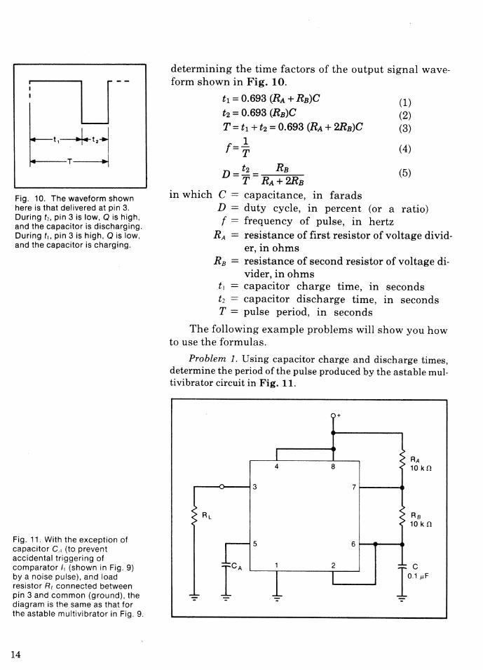
The manufacturer of an astable multivibrator has provided the following list of formulas that can be used for
13
--I I
.-t,-----.j.-t.,
T ... I
Fig. 10. The waveform shown here is that delivered at pin 3. During t2, pin 3 is low, Q is high, and the capacitor is discharging. During t1, pin 3 is high, Q is low, and the capacitor is charging.
Fig. 11. With the exception of capacitor C, (to prevent accidental triggering of comparator /1 (shown in Fig. 9) by a noise pulse), and load resistor R1 connected between pin 3 and common (ground), the diagram is the same as that for the astable multivibrator in Fig. 9.
14
determining the time factors of the output signal waveform shown in Fig. 10.
tl = 0.693 (RA + RB)C (1) t2 = 0.693 (RB)C (2) T = t1 + t2 = 0.693 (RA + 2RB)C (3)
1 {=- (4) T
D = t2 = RB (5) T RA+2RB
in which C = capacitance, in farads D = duty cycle, in percent (or a ratio) f = frequency of pulse, in hertz
RA resistance of first resistor of voltage divider, in ohms
Rs = resistance of second resistor of voltage di-vider, in ohms
t1 = capacitor charge time, in seconds t2 = capacitor discharge time, in seconds T = pulse period, in seconds
The following example problems will show you how to use the formulas.
Problem 1. Using capacitor charge and discharge times, determine the period of the pulse produced by the astable multivibrator circuit in Fig. 11.
+
RA 4 8 10 kn
3 7
RL Ra 10 k n
5 6
2 c 101 "' -=- -=- -:- -=-
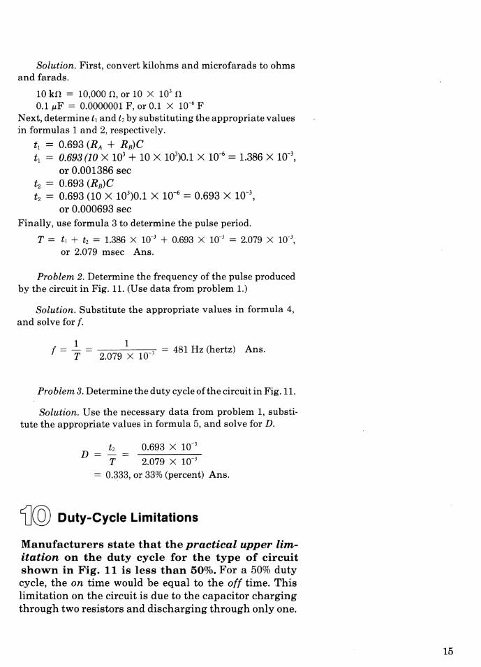
Solution. First, convert kilohms and microfarads to ohms and farads.
10 kn = 10,000 n, or 10 x 103 n 0.1 J.LF = 0.0000001 F, or 0.1 X 10⁻⁶ F
Next, determine t1 and t2 by substituting the appropriate values in formulas 1 and 2, respectively.
t 1 0.693 (RA + Rn)C t1 = 0.693 (10 X 103 + 10 X 103)0.1 X 10-6 = 1.386 X 10⁻³,
or 0.001386 sec t 2 = 0.693 (Rn)C t2 = 0.693 (10 X 103)0.1 X 10-6 = 0.693 X 10-\
or 0.000693 sec Finally, use formula 3 to determine the pulse period.
T = t1 + t2 = 1.386 X 10⁻³ + 0.693 X 10-3 = 2.079 X 10⁻³,
or 2.079 msec Ans.
Problem 2. Determine the frequency of the pulse produced by the circuit in Fig. 11. (Use data from problem 1.)
Solution. Substitute the appropriate values in formula 4, and solve for f.
1 1 A f = T = 2.079 X 10_3 = 481 Hz (hertz) ns.
Problem 3. Determine the duty cycle of the circuit in Fig. 11.
Solution. Use the necessary data from problem 1, substitute the appropriate values in formula 5, and solve for D.
D 0.693 X 10⁻³
2.079 X 10-3
= 0.333, or 33% (percent) Ans.
1]@ Duty-Cycle Limitations
Manufacturers state that the practical upper limitation on the duty cycle for the type of circuit shown in Fig. 11 is less than 50%. For a 50% duty cycle, the on time would be equal to the off time. This limitation on the circuit is due to the capacitor charging through two resistors and discharging through only one.
15
16
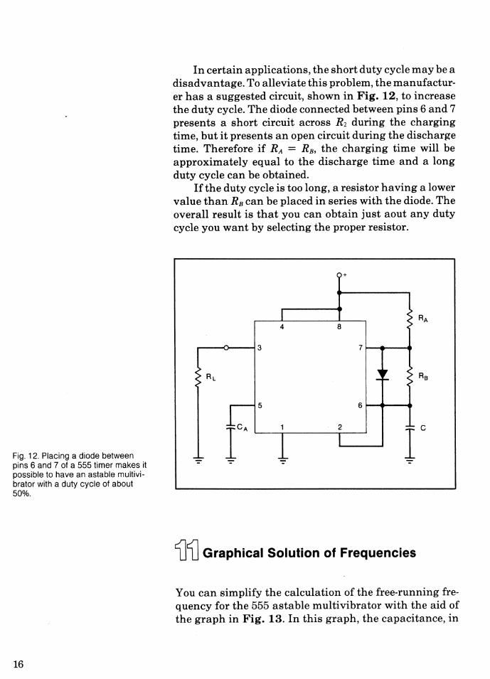
In certain applications, the short duty cycle may be a disadvantage. To alleviate this problem, the manufacturer has a suggested circuit, shown in Fig. 12, to increase the duty cycle. The diode connected between pins 6 and 7 presents a short circuit across Rz during the charging time, but it presents an open circuit during the discharge time. Therefore if RA = RB, the charging time will be approximately equal to the discharge time and a long duty cycle can be obtained.
If the duty cycle is too long, a resistor having a lower value than RB can be placed in series with the diode. The overall result is that you can obtain just aout any duty cycle you want by selecting the proper resistor.
+
1}1} Graphical Solution of Frequencies
You can simplify the calculation of the free-running frequency for the 555 astable multivibrator with the aid of the graph in Fig. 13. In this graph, the capacitance, in
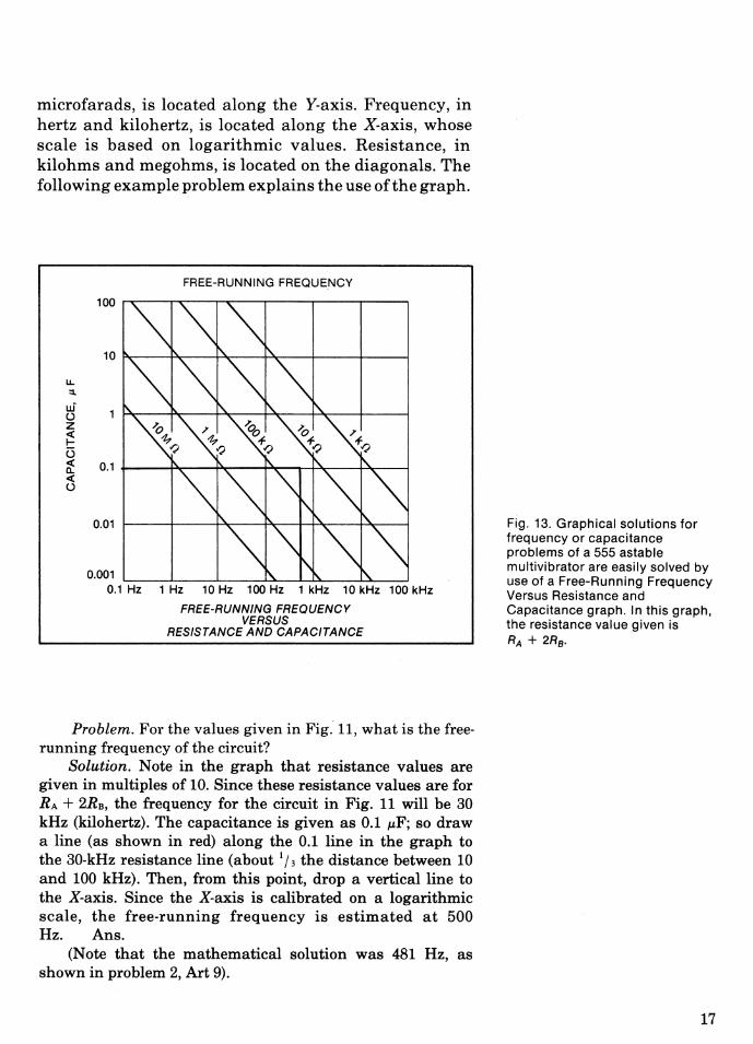
microfarads, is located along the Y-axis. Frequency, in hertz and kilohertz, is located along the X-axis, whose scale is based on logarithmic values. Resistance, in kilohms and megohms, is located on the diagonals. The following example problem explains the use of the graph.
u. ::1.
w (.) z ~ C3
FREE-RUNNING FREQUENCY
~ 0.1 ~--~~---P~--~~~~--~~--~ <( (.)
0.001 L..-----.l.--....1...--...1...3o..-.L.J~---'-...__-----' 0.1 Hz 1 Hz 10Hz 100Hz 1 kHz 10kHz 100kHz
FREE-RUNNING FREQUENCY VERSUS
RESISTANCE AND CAPACITANCE
Problem. For the values given in Fig: 11, what is the freerunning frequency of the circuit?
Solution. Note in the graph that resistance values are given in multiples of 10. Since these resistance values are for RA + 2Ra, the frequency for the circuit in Fig. 11 will be 30 kHz (kilohertz). The capacitance is given as 0.1 #LF; so draw a line (as shown in red) along the 0.1 line in the graph to the 30-kHz resistance line (about 113 the distance between 10 and 100 kHz). Then, from this point, drop a vertical line to the X-axis. Since the X-axis is calibrated on a logarithmic scale, the free-running frequency is estimated at 500 Hz. Ans.
(Note that the mathematical solution was 481 Hz, as shown in problem 2, Art 9).
Fig. 13. Graphical solutions for frequency or capacitance problems of a 555 astable multivibrator are easily solved by use of a Free-Running Frequency Versus Resistance and Capacitance graph. In this graph, the resistance value given is RA + 2R8 .
17
R
TOUCH PLATE
R,
R2 CI '::" -=-
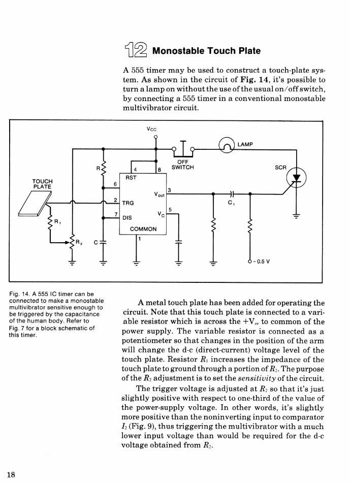
Fig. 14. A 555 IC timer can be connected to make a monostable multivibrator sensitive enough to be triggered by the capacitance of the human body. Refer to Fig. 7 for a block schematic of this timer.
18
1]~ Monostable Touch Plate
A 555 timer may be used to construct a touch-plate system. As shown in the circuit of Fig. 14, it's possible to turn a lamp on without the use ofthe usual on/ off switch, by connecting a 555 timer in a conventional monostable multivibrator circuit.
Vee
LAMP
OFF 4 8 SWITCH
RST
Vout 3
TRG c,
DIS Ve 5
'::"
COMMON
I -0.5 v '::" '::" '::"
A metal touch plate has been added for operating the circuit. Note that this touch plate is connected to a variable resistor which is across the +Vee to common of the power supply. The variable resistor is connected as a potentiometer so that changes in the position of the arm will change the d-e (direct-current) voltage level of the touch plate. Resistor R1 increases the impedance of the touch plate to ground through a portion of R2. The purpose ofthe R2 adjustment is to set the sensitivity of the circuit.
The trigger voltage is adjusted at R2 so that it's just slightly positive with respect to one-third of the value of the power-supply voltage. In other words, it's slightly more positive than the noninverting input to comparator !2 (Fig. 9), thus triggering the multivibrator with a much lower input voltage than would be required for the d-e voltage obtained from R2.
1J®operation of Touch-Plate System
When body contact is made with the touch plate, the capacitance of the body reduces the impedance of the circuit at the trigger. This momentary lowering of the d-e voltage triggers the monostable multivibrator. The result is a logic 1 at the output on pin 3.
The time constant of R and C must be made long enough so that the monostable output will occur at a logic 1 for a period longer than that for touching the plate. Another way of saying this is: The monostable output must be high at the time the touch plate is released. The reason is that noise pulses- created when the touch plate is released - can inject noise into the system and retrigger the 555 timer.
The positive output from Vout is delivered through capacitor C1 to the gate of the SCR (silicon-controlled rectifier). This gate is maintained at a slightly negative voltage at all times except when the pulse is applied. The reason for the slightly negative bias voltage is to prevent the SCR from being accidentally triggered on by a stray noise spike.
After the logic 1 has been delivered to the gate, the SCR is turned on. Even though the output of the 555 timer returns to a low condition, the SCR is not affected. The negative voltage that occurs on the SCR gate cannot turn the SCR off, since it is a thyristor in the HOLD condition.
When the SCR conducts, the lamp lights and remains lit until the push-button off switch is operated. Keep in mind that the only way you can shut an SCR off is to stop the current from flowing in the anode circuit. This is the purpose of the off switch.
1]~ Operation of A-C Circuits
Instead of the lamp in Fig. 14, the SCR may be used to operate a relay which can, in turn, operate high-voltage a-c (alternating-current) circuits, such as those needed for 110-V (volt) lamps and a-c motors.
There is an important precaution regarding the use of relays with a 555 timer. If the 555 timer is used to directly operate an inductive load of any
19
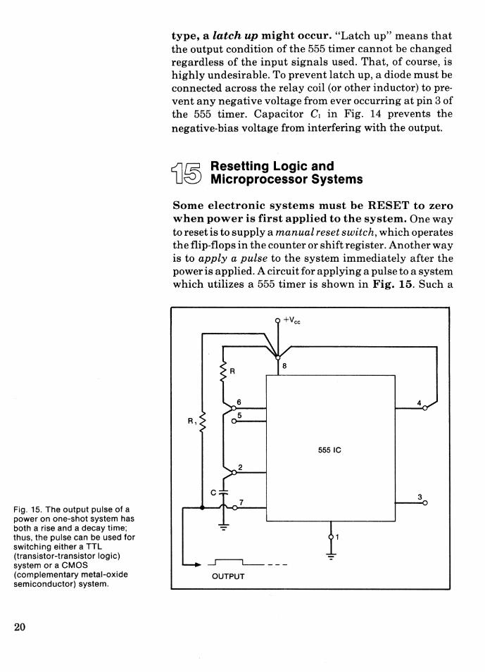
Fig. 15. The output pulse of a power on one-shot system has both a rise and a decay time; thus, the pulse can be used for switching either a TTL (transistor-transistor logic) system or a CMOS (complementary metal-oxide semiconductor) system.
20
type, a latch up might occur. "Latch up" means that the output condition of the 555 timer cannot be changed regardless of the input signals used. That, of course, is highly undesirable. To prevent latch up, a diode must be connected across the relay coil (or other inductor) to prevent any negative voltage from ever occurring at pin 3 of the 555 timer. Capacitor C1 in Fig. 14 prevents the negative-bias voltage from interfering with the output.
c::1/E2. Resetting Logic and U~ Microprocessor Systems
Some electronic systems must be RESET to zero when power is first applied to the system. One way to reset is to supply a manual reset switch, which operates the flip-flops in the counter or shift register. Another way is to apply a pulse to the system immediately after the power is applied. A circuit for applying a pulse to a system which utilizes a 555 timer is shown in Fig. 15. Such a
R,
2
c 7
~--
OUTPUT
4
5551C
3
system is referred to as a power on one-shot, a power up one-shot, or a power-supply reset system.
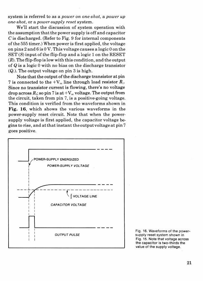
We'll start the discussion of system operation with the assumption that the power supply is off and capacitor Cis discharged. (Refer to Fig. 9 for internal components ofthe 555 timer.) When power is first applied, the voltage on pins 2 and 6 is 0 V. This voltage causes a logic 0 on the SET (S) input of the flip-flop and a logic 1 on the RESET (R). The flip-flop is low with this condition, and the output of Q is a logic 0 with no bias on the discharge transistor (QJ). The output voltage on pin 3 is high.
Note that the output ofthe discharge transistor at pin 7 is connected to the +Vee line through load resistor R1. Since no transistor current is flowing, there's no voltage drop across R1; so pin 7 is at+ Vee voltage. The output from the circuit, taken from pin 7, is a positive-going voltage. This condition is verified from the waveforms shown in Fig. 16, which shows the various waveforms in the power-supply reset circuit. Note that when the powersupply voltage is first applied, the capacitor voltage begins to rise, and at that instant the output voltage at pin 7 goes positive.
_j.-f;-PO-W-ER---S-U-PP_L_Y_E_N_E_RG-IZ_E_D ___ - ---
1 POWER-SUPPLY VOLTAGE I I I I I I ----
___ .!.._- --------------------
1 1 \ ~VOLTAGE LINE I 3 I I I I I
CAPACITOR VOLTAGE
__ll!---------1 I I I
OUTPUT PULSE Fig. 16. Waveforms of the powersupply reset system shown in Fig. 15. Note that voltage across the capacitor is two-thirds the value of the supply voltage.
21
22
As the capacitor continues to charge, it will eventually reach a value that is two-thirds of the power-supply voltage. At that instant, the voltage on pin 6 will exceed the voltage on pin 5 and the output of comparator !1 will go to a logic 1 condition. At the same time, the output of comparator !2 is at a logic 0 so the flip-flop has been switched to a high condition.
A logic 1 is thus produced at the Q output of the flip-flop, causing the discharge transistor ( Q1) to go into saturation. Now the voltage of pin 7 is virtually ground. (It's different from ground only by the forward voltage drop across Q1, which is in saturation). The output signal at that instant goes low. The short-duration output pulse can be used to reset (or set) the flip-flops in logic and microprocessor circuits.
As shown in Fig. 16, the capacitor continues to charge until it reaches its maximum value, which will be approximately equal to the +Vee value for the system. Since there's no way to discharge the capacitor, there's no further change in the output voltage.
Check Your Learning 2
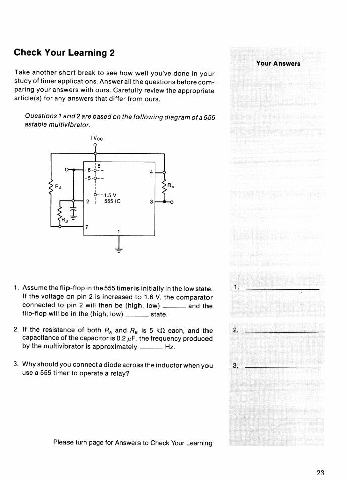
Take another short break to see how well you've done in your study of timer applications. Answer all the questions before comparing your answers with ours. Carefully review the appropriate article(s) for any answers that differ from ours.
Questions 1 and 2 are based on the following diagram of a 555 astable mu/tivibrator.
+Vee
:a ~t--+6-9-- 4
-5-0--1 I I I o--1.5 v
r---o--i 2 : 555 IC 3
1. Assume the flip-flop in the 555 timer is initially in the low state. If the voltage on pin 2 is increased to 1.6 V, the comparator connected to pin 2 will then be (high, low) and the flip-flop will be in the (high, low) state.
2. If the resistance of both RA and R8 is 5 kO each, and the capacitance of the capacitor is 0.2 J.LF, the frequency produced by the multivibrator is approximately Hz.
3. Why should you connect a diode across the inductor when you use a 555 timer to operate a relay?
Please turn page for Answers to Check Your Learning
24
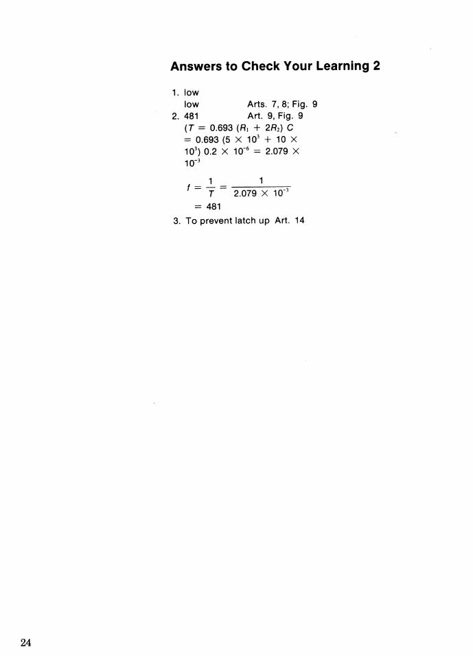
Answers to Check Your Learning 2
1. low low Arts. 7, 8; Fig. 9
2. 481 Art. 9, Fig. 9 (T = 0.693 (Rt + 2R2) C = 0. 693 ( 5 X 1 03 + 1 0 X 1 03 ) 0.2 X 10-6 = 2.079 X 1 o-3
1 f = T = 2.079 X 1 0 3
= 481
3. To prevent latch up Art. 14
Industrial Applications of Pulse and Switching Circuits
1]@ Telemetering
Telemetering means measuring at a distance. It is important in industrial electronic measurements because, in many applications, the operator is not close to all the measurements needed to perform the job. In such cases, the measurements are transmitted as data in the form of pulses If the data is in analog form, that is, if it's continually variable, an analog-to-digital converter is needed to convert the data into a string of pulses that can be readily transmitted.
Most telemetering, and almost all data transmission, is in the form of pulses. There are two reasons for the use of pulses: The first is that pulse transmission is much more efficient because of the relatively long resting period between the pulses. Electronic equipment is just like human beings in that sense. If you give it time to rest, it can perform more efficiently. The second reason is that pulse transmission can be made relatively free of noise by adjusting the receiving equipment so that it's sensitive only to the individual pulses.
25
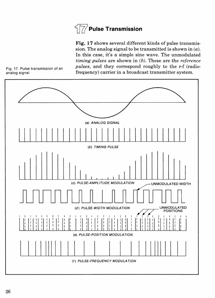
Fig. 17. Pulse transmission of an analog signal
1]~ Pulse Transmission
Fig. 17 shows several different kinds of pulse transmission. The analog signal to be transmitted is shown in (a). In this case, it's a simple sine wave. The unmodulated timing pulses are shown in (b). These are the reference pulses, and they correspond roughly to the r-f (radiofrequency) carrier in a broadcast transmitter system.
(a) ANALOG SIGNAL
1111111111111111111111111111111 (b) TIMING PULSE
I I I I I I (c) PULSE-AMPLITUDE MODULATION
I I I I I
(d) PULSE-WIDTH MODULATION ,---,...---,.----UNMODULATED //7 POSITIONS
I I I I I I I I I I I I I I I I I I I I I I I I I I I I I I I I I I I I
I I' I I I I I I I I I I I I I I I I I I I I I I I I I I I I I I I I I I I I I I I I I I I I I I I I I I I I : I I I I I I : : : I : ! I
,I I I I I I I I II I I I I I I I I I I I I
(e) PULSE-POSITION MODULATION
I I II IIIII I I I I I I I I 1111111 I I (f) PULSE-FREQUENCY MODULATION
26
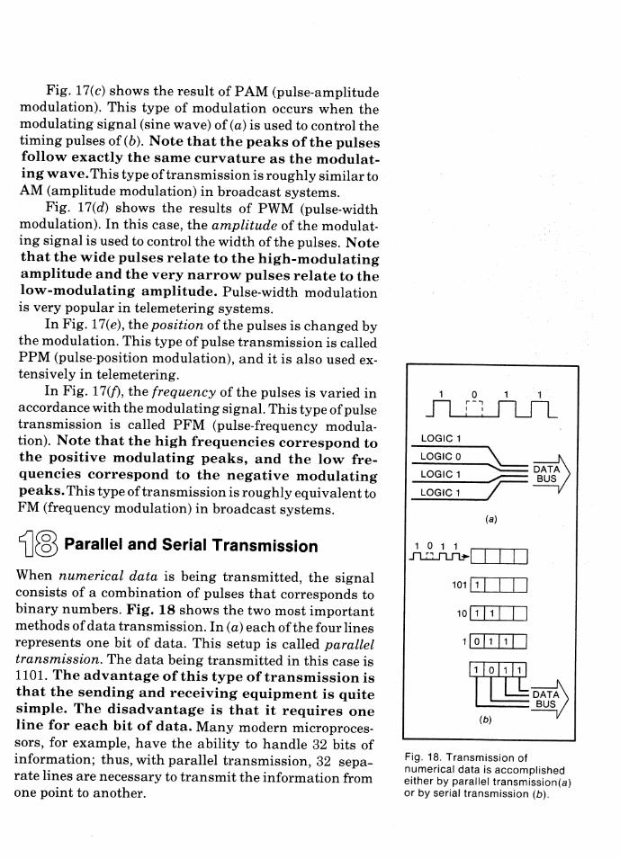
Fig. 17(c) shows the result of PAM (pulse-amplitude modulation). This type of modulation occurs when the modulating signal (sine wave) of (a) is used to control the timing pulses of(b). Note that the peaks ofthe pulses follow exactly the same curvature as the modulating wave. This type of transmission is roughly similar to AM (amplitude modulation) in broadcast systems.
Fig. 17(d) shows the results of PWM (pulse-width modulation). In this case, the amplitude of the modulating signal is used to control the width of the pulses. Note that the wide pulses relate to the high-modulating amplitude and the very narrow pulses relate to the low-modulating amplitude. Pulse-width modulation is very popular in telemetering systems.
In Fig. 17(e), the position of the pulses is changed by the modulation. This type of pulse transmission is called PPM (pulse-position modulation), and it is also used extensively in telemetering.
In Fig. 17({), the frequency of the pulses is varied in accordance with the modulating signal. This type of pulse transmission is called PFM (pulse-frequency modulation). Note that the high frequencies correspond to the positive modulating peaks, and the low frequencies correspond to the negative modulating peaks. This type of transmission is roughly equivalent to FM (frequency modulation) in broadcast systems.
1]@ Parallel and Serial Transmission
When numerical data is being transmitted, the signal consists of a combination of pulses that corresponds to binary numbers. Fig. 18 shows the two most important methods of data transmission. In (a) each of the four lines represents one bit of data. This setup is called parallel transmission. The data being transmitted in this case is 1101. The advantage of this type of transmission is that the sending and receiving equipment is quite simple. The disadvantage is that it requires one line for each bit of data. Many modern microprocessors, for example, have the ability to handle 32 bits of information; thus, with parallel transmission, 32 separate lines are necessary to transmit the information from one point to another.
1 0 1 ., n ;-: n n
..J L...1...._!___! LJ L
LOGIC 1
~~ ~DATA ~BUS
~ (a)
1 0 1 1 ~.._I ...___,_---~.1__.1
1 o 1 IL...1....LI---L.---L..---'
10 l1 l1 I
1l o l1 l1 I
(b)
~ ~
Fig. 18. Transmission of numerical data is accomplished either by parallel transmission(a) or by serial transmission (b).
Fig. 18(b) shows how serial transmission is used to send the same data. With this method, a pulse represents a binary 1 and an absence of a pulse represents a binary 0. In order for this data to be used by a microprocessor or computer, it's necessary to convert the data into a parallel data configuration. A shift register may be used for this conversion. The data enters the shift register one bit at a time. (To accomplish this, a system clock is necessary. The clock is nothing more than a series of pulses used for timing the information into the shift register.) As you can see from the illustration, the bits enter the shift register one at a time until the register is full. Then, the data is unloaded onto the four-line bus. (A bus is simply a combination of conductors used to transmit data.)
lJ@ Digital Voltmeters
Fig. 19 shows how a d-e voltage can be measured and displayed as a digit on a simple digital voltmeter. To understand this system, you must first understand the ramp voltage that is applied. As shown in (a), the length of the ramp is made exactly equal to 10 pulses; thus, it takes 10 pulses for the ramp to go from 0 to 10 V. In practice, however, any number of pulses can be used, but it's easier to describe ramp voltage by using just 10.
The heart of the system is the comparator shown in Fig.19(b). The unknown voltage to be measured is applied to one input of the comparator, and the ramp voltage to the other input. This comparator is really an op amp (operational amplifier) designed to have a very high slewing rate. A high slewing rate means that when the ramp voltage becomes more positive than the unknown voltage, the output will switch very rapidly.
As shown by the dashed lines in (c), if only the ramp voltage is applied to the comparator, the output will be a square wave that corresponds to the width of the ramp. Now let's assume th;:1t the unknown voltage to be measured is 4 V. As shown by the solid lines, the comparator output starts positive at the beginning of the ramp and continues until the ramp voltage becomes equal to the unknown yoltage. At that instant, the comparator switches to a low condition. Thus, the comparator output
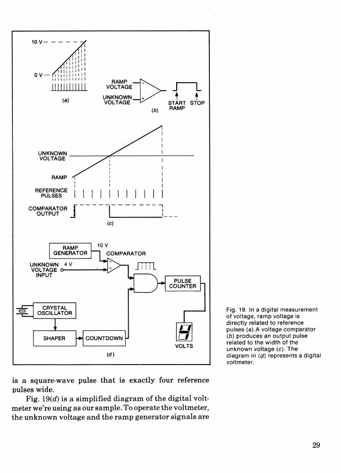
10V-----I I
I II ,till
11 I\ I I 'I til I I
till Ill 11111111 11
OV-,tltlttltlll 1 I II 1 I I I I I I I
111111111111
(a)
RAMP
RAMP!>-VOLTAGE ~ UNKNOWN + t t VOLTAGE START STOP
(b) RAMP
I I I I I
REFERENCE PULSES I I I I I I
COMPARATOR J -----~- ------ ~ OUTPUT 1 __ _
RAMP GENERATOR
UNKNOWN 4 V
(c)
VOLTAGE &-------~~ INPUT
COUNTDOWN
(d)
VOLTS
is a square-wave pulse that is exactly four reference pulses wide.
Fig. 19(d) is a simplified diagram of the digital voltmeter we're using as our sample. To operate the voltmeter, the unknown voltage and the ramp generator signals are
Fig. 19. In a digital measurement of voltage, ramp voltage is directly related to reference pulses (a).A voltage comparator (b) produces an output pulse related to the width of the unknown voltage (c). The diagram in (d) represents a digital voltmeter.
29
applied to the comparator. The comparator output, a square-wave pulse that is exactly four reference pulses wide, is applied to one input of an AND gate. (Of course, if the unknown voltage was higher, there would be more pulses; and if it was lower, there would be fewer pulses.) A crystal oscillator signal, which has been shaped into pulses and counted down to a very precise frequency of pulses, is applied to the other input of the AND gate. The AND gate, which is used as an enable, permits four pulses to pass through. The four pulses are counted by the counter and displayed on the digital display. Thus, the digital display shows the number of volts applied at the input of the voltmeter.
~@ Digital Capacitance Meter
Fig. 20 shows how the 3905 timer can be used to make a digital capacitance meter. In this system, the unknown capacitor Cx is connected into the time-constant circuit of the 3905 timer. Note that the resistor (R) of this timeconstant circuit is connected to the regulated reference,in the 3905 timer. The logic lead for that timer is connected to the same point. The positive logic connection is used to get a positive output at the collector of the internal power transistor.
The trigger input pulse starts the capacitor on a charge cycle. (The amount of time that it takes the capacitor to charge to a reference is marked Tx on the output signal.) The smaller the capacitor, the less time it will take to complete the output pulse. Likewise, a larger capacitor will produce a broader output pulse.
The output pulse from the 3905 timer is delivered to the AND gate, which is being used as an enable circuit. The crystal oscillator signal, counted down to produce very accurate timing pulses, is also delivered to the enable. The number of timing pulses that passes through the enable depends on the width of Tx, which, in turn, depends on the capacitance of Cx.
+
Jl TRIGGER
B+ C 1--___.-___, -j T X r-
A LOGIC Jl._
.------!RIC E COMMON
ENABLE
3905..,___ .....
-:-COMMON
llll!llll
CRYSTAL OSCILLATOR SHAPER COUNTDOWN MICROFARADS
The pulse counter counts the pulses and displays the value in microfarads. It is presumed that the system shown in Fig. 20 has been calibrated so that0.2 JLF represents the capacitance involved. The capacitance reading may correspond to 20 pulses or 200 pulses passing through the enable, depending on the calibration of the meter.
~lJ Switching Power Supplies
Always keep in mind that the terms pulse, digital, and switching are used interchangeably in practice, even though each of these terms has its own separate technical meaning. A switching power supply is really a pow-· er supply that employs pulses for its operation.
Fig. 20. Use of a 3905 timer for a digital capacitance meter. Note that resistor R1. is the load resistor for the output transistor.
Fig. 21. The pulse generator in this diagram of a switching power supply, or converter, could be either a 555 timer or a multivibrator.
32
Fig. 21 shows an example of a switching power supply. Before the terms "digital" and "pulse" became so popular, this type of system was known as an oscillator power supply. It's technically classified as a converter, which is a type of power supply that changes a d-e voltage from one voltage value to a higher voltage value.
POWER AMPLIFIER
The pulse generator, voltage amplifier, and power amplifier are operated from a 12-V supply, and are as
sumed to be bipolar transistor circuits. Output pulses from the pulse generator are amplified by a voltage amplifier, and then delivered to a power amplifier. The power amplifier output goes to the primary of an output transformer. Usually, with this type of supply, there are a
number of secondaries. In the system shown here, there's a 150-V secondary and a 50-V secondary. Each of these secondaries is connected to a half-wave rectifier and a filter to convert the pulse waveform into d-e voltages.
One reason for the popularity of this type of power supply is that it can be operated from a low d-e voltage, and therefore, it's possible to obtain relatively high voltages in transistorized portable equipment. Another reason is that the pulse generator can be one that produces a high frequency. High-frequency transformers can be
made smaller than low-frequency ones. So, the output transformer in the circuit of Fig. 21 can be much smaller
than the bulky and heavy power transformers used on 60-Hz lines. It's because of the lighter weight- and corresponding savings in space and cost- that this type of power supply has become popular in television receivers and industrial monitors.
In modern equipment, you'll find the switching power supply being used, even though the system operates from an a-c power line. An a-c low-voltage power supply is used only to supply the 12 V necessary to operate the circuitry.
~~ Switching Regulators
Digital circuits are also used in regulator supplies. Refer to Fig. 22, which shows the influence of pulse width on the d-e average value (AVE) of a pulse. (The average value is related to the voltage after rectification.) In (a), the pulse is actually a square wave. The average value of a square wave is 50% of pulse amplitude. In (b), the pulse is wider, which results in a higher d-e average value. Conversely, in (c), the pulse is narrower, which produces a lower output average value.
The input and output characteristics of the pulses just described are those produced by the switching regulator shown in Fig. 23. An oscillator is used to produce a
START-UP
ELECTRONIC SWITCH
rl rl ll_AVE _J LJ LJ L-ov
(a)
r-J r-1 rl -AVE _J U U L- ov
(b)
n n n _AVE _J L__J L__j L__ - 0 v
(c)
Fig. 22. The average output voltage value of a pulsed waveform depends on the width of the pulses. A normal square waveform is shown in (a), while (b) and (c) show wider and narrower pulses, respectively.
Fig. 23. A switching regulator controls the output of a power supply by varying the width of square-wave pulses.
33
34
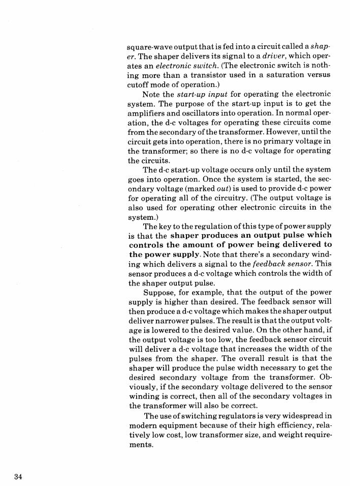
square-wave output that is fed into a circuit called a shaper. The shaper delivers its signal to a driver, which operates an electronic switch. (The electronic switch is nothing more than a transistor used in a saturation versus cutoff mode of operation.)
Note the start-up input for operating the electronic system. The purpose of the start-up input is to get the amplifiers and oscillators into operation. In normal operation, the d-e voltages for operating these circuits come from the secondary of the transformer. However, until the circuit gets into operation, there is no primary voltage in the transformer; so there is no d-e voltage for operating the circuits.
The d-e start-up voltage occurs only until the system goes into operation. Once the system is started, the secondary voltage (marked out) is used to provide d-e power for operating all of the circuitry. (The output voltage is also used for operating other electronic circuits in the system.)
The key to the regulation ofthis type of power supply is that the shaper produces an output pulse which controls the amount of power being delivered to the power supply. Note that there's a secondary winding which delivers a signal to the feedback sensor. This sensor produces a d-e voltage which controls the width of the shaper output pulse.
Suppose, for example, that the output of the power supply is higher than desired. The feedback sensor will then produce a d-e voltage which makes the shaper output deliver narrower pulses. The result is that the output voltage is lowered to the desired value. On the other hand, if the output voltage is too low, the feedback sensor circuit will deliver a d-e voltage that increases the width of the pulses from the shaper. The overall result is that the shaper will produce the pulse width necessary to get the desired secondary voltage from the transformer. Obviously, if the secondary voltage delivered to the sensor winding is correct, then all of the secondary voltages in the transformer will also be correct.
The use of switching regulators is very widespread in modern equipment because of their high efficiency, relatively low cost, low transformer size, and weight requirements.
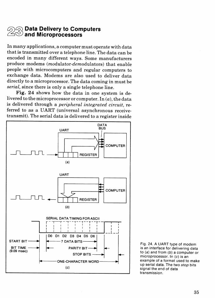
C/))0) Data Delivery to Computers L60 and Microprocessors
In many applications, a computer must operate with data that is transmitted over a telephone line. The data can be encoded in many different ways. Some manufacturers produce modems (modulator-demodulators) that enable people with microcomputers and regular computers to exchange data. Modems are also used to deliver data directly to a microprocessor. The data coming in must be serial, since there is only a single telephone line.
Fig. 24 shows how the data in one system is delivered to the microprocessor or computer. In (a), the data is delivered through a peripheral integrated circuit, referred to as a UART (universal asynchronous receivetransmit). The serial data is delivered to a register inside
START BIT
BIT TIME (9.09 msec)
DATA UART BUS ~--------~/~--~
COMPUTER
(a)
UART
(b)
SERIAL DATA TIMING FOR ASCII ~- ,---r- ~- -T-- T-- T- -r--r-----r---r-1 1 1 I I I I 1 I I I I I I I I I I 1 I I I I _ _ l __ J
~7D~A;:B~T: DS Dlj-:1
j.- PARITY BIT
STOP BITS
!+----ONE-CHARACTER WORD----I~
(c)
Fig. 24. A UART type of modem is an interface for delivering data to (a) and from (b) a computer or microprocessor. In (c) is an example of a format used to make up serial data. The two stop bits signal the end of data transmission.
35
the UART. The data is then delivered from the UART, in parallel, to the microprocessor or computer.
The UART system can be reversed as shown in Fig. 24(b). Here the microprocessor or computer produces a parallel output combination of 1s and Os characteristic of binary-coded data. The parallel data is delivered to a parallel in/ serial out shift register. Once the register is loaded, the data is transmitted out from the UART.
Each modem is unique in the way it makes up serial data. Fig. 24(c) shows one example. Its format requires a single start pulse to show the system when the data has begun. Following this pulse are seven individual pulses that represent the data.
Next, you'll see a parity bit. The purpose of this bit is to show that the data is valid. If there is an even parity requirement for this data, a pulse will be added when the data contains an odd number of 1s. For example, let's suppose the data being sent is 0101010. Since there are three 1s in this transmission, we must add a parity bit so that the microprocessor or computer will know that the information is valid.
Microprocessors and computers are designed to respond only to even parity or odd parity. Thus, the microprocessor will only respond to data that has an even number of 1s (counting the parity bit) when the system is designed for even parity. If the system is designed for odd parity, then the microprocessor or computer will only respond to data with an odd number of 1s (including the parity bit).

Check Your Learning 3
Take another short break before going on to the Self-Test, to review some key points on the application of pulse and switching circuits. Don't shortchange yourself by failing to restudy the appropriate article(s) for any of your answers that differ from ours.
1. When you measure data from a remote position, you would 1. probably use the procedure.
2. Which of the following pulse modulations is somewhat similar 2. to the signal broadcast by an AM transmitter?
A Pulse amplitude B. Pulse frequency C. Pulse width
3. List the two principal methods of data transmission. 3.
4. What is the function of the crystal oscillator in a digital 4. voltmeter?
5. Which one of the following pulse forms has the lower average 5. voltage value?
A.
B.
Answers to Check Your Learning 3
~~ ·61.::1 ·~~ ·pv ~·g·g
6 ~ "lJ\f S8Sind 6U!UJ!l aJemooe aonpoJd 0.1 ·v
IB!J8S "£ H "lJ\f apnJ!IdUJe as1nd ·v ·~
g ~ ·pv 6upaJaUJalaJ · ~
37
38
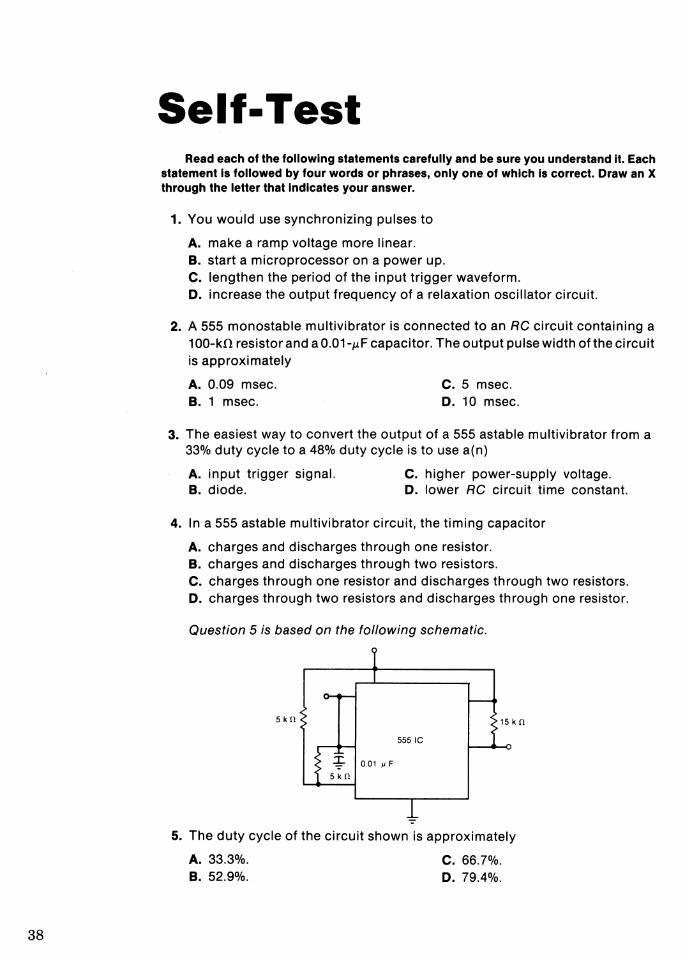
Self-Test Read each of the following statements carefully and be sure you understand it. Each
statement Is followed by four words or phrases, only one of which Is correct. Draw an X through the letter that Indicates your answer.
1. You would use synchronizing pulses to
A. make a ramp voltage more linear. B. start a microprocessor on a power up. C. lengthen the period of the input trigger waveform. D. increase the output frequency of a relaxation oscillator circuit.
2. A 555 monostable multivibrator is connected to an RC circuit containing a 1 00-kO resistor and a 0.01-J.LF capacitor. The output pulse width of the circuit is approximately
A. 0.09 msec. C. 5 msec. B. 1 msec. D. 10 msec.
3. The easiest way to convert the output of a 555 astable multivibrator from a 33% duty cycle to a 48% duty cycle is to use a(n)
A. input trigger signal. C. higher power-supply voltage. B. diode. D. lower RC circuit time constant.
4. In a 555 astable multivibrator circuit, the timing capacitor
A. charges and discharges through one resistor. B. charges and discharges through two resistors. C. charges through one resistor and discharges through two resistors. D. charges through two resistors and discharges through one resistor.
Question 5 is based on the following schematic.
5 kll 15 k n
5551C
.:;:!;. O.Q1 ll F
5 kll
5. The duty cycle of the circuit shown is approximately
A. 33.3%. C. 66. 7%. B. 52.9%. D. 79.4%.
6. The 555 touch-plate circuit is basically a
A. crowbar circuit C. monostable multivibrator. B. digital oscillator. D. power amplifier.
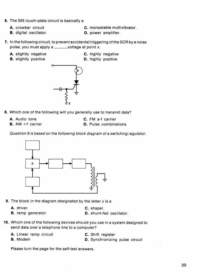
7. In the following circuit, to prevent accidental triggering of the SCR by a noise pulse, you must apply a voltage at point x.
A. slightly negative C. highly negative B. slightly positive D. highly positive
8. Which one of the following will you generally use to transmit data?
A. Audio tone C. FM a-f carrier B. AM r-f carrier D. Pulse combinations
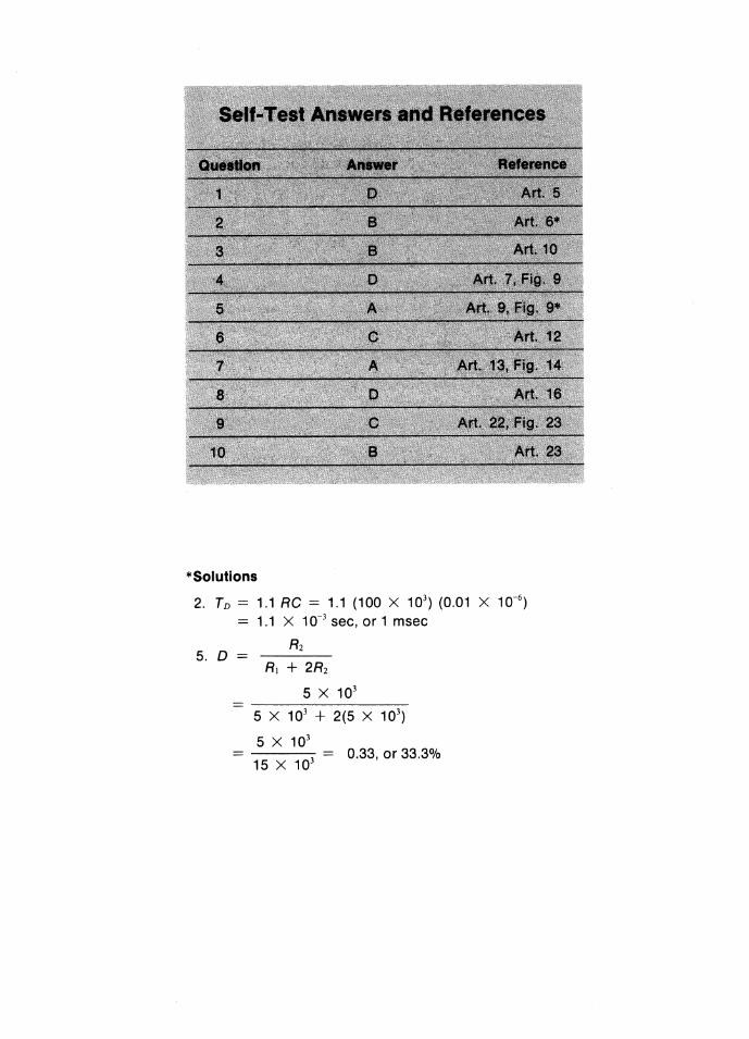
Question 9 is based on the following block diagram of a switching regulator.
9. The block in the diagram designated by the letter xis a
A. driver. C. shaper. B. ramp generator. D. shunt-fed oscillator.
10. Which one of the following devices should you use in a system designed to send data over a telephone line to a computer?
A. Linear ramp circuit C. Shift register B. Modem D. Synchronizing pulse circuit
Please turn the page for the self-test answers.
39
*Solutions
2. TD = 1.1 RC = 1.1 (100 X 103) (0.01 X 10⁻⁶)
1.1 X 10⁻³ sec, or 1 msec
5. D
5 X 10³ + 2(5 X 10³)
5 X 10³
---3 = 0.33, or 33.3% 15 X 10
Related Documents


