www.cypress.com Document No. 001-76458 Rev. *F 1 AN76458 PSoC ® 5LP High-Voltage (120-240 VAC) Powerline Communication Solution Author: Jeffrey Hushley Associated Part Family: CY8C56xx/CY8C58xx Associated Project: Yes Related Application Notes: AN77759 - Getting Started with PSoC ® 5LP AN58825 - PLC - Powerline Communication Debugging Tools To get the latest version of this application note, or the associated project file, please visit http://www.cypress.com/go/AN76458 . AN76458 describes how to develop a complete powerline communication system with the PSoC 5LP family of devices. Attached to the application note is a code example of a 2400-bps FSK modem with the Cypress powerline network protocol. Also attached are design files of a board that interfaces the PSoC 5LP device to a high-voltage (120-240 VAC) powerline. Contents 1 Introduction .............................................................1 2 PLC on PSoC 5LP Architecture ..............................3 2.1 FSK Modulator ......................................................4 2.2 FSK Demodulator .................................................5 2.3 Network Protocol ..................................................5 3 Application Programming Interface (API) ...............8 3.1 Steps to Transmit a Packet ...................................8 3.2 Steps to Receive a Packet ....................................8 4 Host Interface (Optional) ........................................9 4.1 I2C Interface .........................................................9 4.2 UART and SPI .................................................... 10 5 External Hardware ................................................ 11 5.1 PLC Device ......................................................... 13 5.2 Transmit Filter ..................................................... 14 5.3 Transmit Amplification ........................................ 17 5.4 Receive Filter ...................................................... 20 5.5 Coupling Circuit .................................................. 21 6 Performance ......................................................... 24 6.1 Transmitter Conducted Emissions ...................... 24 6.2 Transmission with Heavy Loads ......................... 25 6.3 Receiver Input Sensitivity ................................... 26 6.4 Receiver Noise Immunity .................................... 30 7 How to Debug PLC............................................... 35 7.1 Causes of Poor Performance ............................. 35 7.2 Methods to Improve Performance ...................... 35 8 Code Example Evaluation .................................... 36 8.1 Standalone Demo Evaluation ............................. 37 8.2 External Host Interface Evaluation ..................... 41 9 Summary .............................................................. 43 A Appendix A: PLC Configuration Array .................. 44 B Appendix B: PSoC 5LP PLC Hardware User’s Guide .................................................................... 50 B.1 Board Component Description............................ 51 Document History............................................................ 57 Worldwide Sales and Design Support ............................. 58 1 Introduction Powerline communication (PLC) provides a mechanism to exchange data over existing powerlines. The primary benefit of PLC over most other communication methods is that there are no infrastructure costs (i.e., no new wires) to install a PLC-enabled system. There are generally two types of PLC systems: high-bandwidth (video, audio, and so on) and low-bandwidth (command and control). This application note describes how to implement a low-bandwidth, half-duplex PLC solution with the PSoC 5LP family of devices. Figure 1 shows a PLC system diagram. The following sections describe the dark grey boxes in detail.

Welcome message from author
This document is posted to help you gain knowledge. Please leave a comment to let me know what you think about it! Share it to your friends and learn new things together.
Transcript
www.cypress.com Document No. 001-76458 Rev. *F 1
AN76458
PSoC® 5LP High-Voltage (120-240 VAC) Powerline Communication Solution
Author: Jeffrey Hushley
Associated Part Family: CY8C56xx/CY8C58xx
Associated Project: Yes
Related Application Notes: AN77759 - Getting Started with PSoC® 5LP
AN58825 - PLC - Powerline Communication Debugging Tools
To get the latest version of this application note, or the associated project file, please visit http://www.cypress.com/go/AN76458.
AN76458 describes how to develop a complete powerline communication system with the PSoC 5LP family of
devices. Attached to the application note is a code example of a 2400-bps FSK modem with the Cypress powerline
network protocol. Also attached are design files of a board that interfaces the PSoC 5LP device to a high-voltage
(120-240 VAC) powerline.
Contents
1 Introduction ............................................................. 1 2 PLC on PSoC 5LP Architecture .............................. 3 2.1 FSK Modulator ...................................................... 4 2.2 FSK Demodulator ................................................. 5 2.3 Network Protocol .................................................. 5
3 Application Programming Interface (API) ............... 8 3.1 Steps to Transmit a Packet ................................... 8 3.2 Steps to Receive a Packet .................................... 8
4 Host Interface (Optional) ........................................ 9 4.1 I2C Interface ......................................................... 9 4.2 UART and SPI .................................................... 10
5 External Hardware ................................................ 11 5.1 PLC Device ......................................................... 13 5.2 Transmit Filter ..................................................... 14 5.3 Transmit Amplification ........................................ 17 5.4 Receive Filter ...................................................... 20 5.5 Coupling Circuit .................................................. 21
6 Performance ......................................................... 24
6.1 Transmitter Conducted Emissions ...................... 24 6.2 Transmission with Heavy Loads ......................... 25 6.3 Receiver Input Sensitivity ................................... 26 6.4 Receiver Noise Immunity .................................... 30
7 How to Debug PLC ............................................... 35 7.1 Causes of Poor Performance ............................. 35 7.2 Methods to Improve Performance ...................... 35
8 Code Example Evaluation .................................... 36 8.1 Standalone Demo Evaluation ............................. 37 8.2 External Host Interface Evaluation ..................... 41
9 Summary .............................................................. 43 A Appendix A: PLC Configuration Array .................. 44 B Appendix B: PSoC 5LP PLC Hardware User’s
Guide .................................................................... 50 B.1 Board Component Description ............................ 51
Document History ............................................................ 57 Worldwide Sales and Design Support ............................. 58
1 Introduction
Powerline communication (PLC) provides a mechanism to exchange data over existing powerlines. The primary benefit of PLC over most other communication methods is that there are no infrastructure costs (i.e., no new wires) to install a PLC-enabled system.
There are generally two types of PLC systems: high-bandwidth (video, audio, and so on) and low-bandwidth (command and control). This application note describes how to implement a low-bandwidth, half-duplex PLC solution with the PSoC 5LP family of devices. Figure 1 shows a PLC system diagram. The following sections describe the dark grey boxes in detail.

PSoC® 5LP High-Voltage (120-240 VAC) Powerline Communication Solution
www.cypress.com Document No. 001-76458 Rev. *F 2
Figure 1. PLC System Diagram
PSoC 5LP
(FSK Modem,
Network Protocol,
Application Processor)
Coupling Circuit
Power Supply
PLC
Data
Inputs (Voltage/Current,
Temperature, Buttons,
CapSense)
Outputs (LCD, LEDs)
Communication (USB,
RS232, I2C, Ethernet,
Wireless)
P
o
w
e
r
l
i
n
e
PLC-Enabled Equipment
PSoC 5LP
(FSK Modem,
Network Protocol,
Application Processor)
Coupling Circuit
Power Supply
PLC
Data
Inputs (Voltage/Current,
Temperature, Buttons,
CapSense)
Outputs (LCD, LEDs)
Communication (USB,
RS232, I2C, Ethernet,
Wireless)
PLC-Enabled Equipment
More specifically, this application note describes how to:
Use the FSK Modulator and FSK Demodulator components, which reliably transmit and receive data over the powerline, even in the presence of noise and heavy loading on the line.
Use the Network Protocol component, which avoids packet collisions, addresses individual nodes or groups of nodes, corrects single-bit errors (FEC encoding), and detects packet errors (CRC and acknowledgments).
Design hardware that interfaces the PSoC 5LP device to the powerline.
Test the performance of the PLC system and relate it to real-world system performance.
Cypress designed the PLC solution to deliver the best performance for the majority of powerline loading and noise
conditions. Although the Cypress PLC solution has excellent input sensitivity, (<45 dBV) and SNR tolerance (<9 dB in-band), there are situations where the conditions on the line cause communications to degrade. As a result, the best application for this technology is in more controlled power environments. In environments that generate significant noise (such as large industrial systems and large systems of computers) and environments that attenuate the signal (multiple phases), it is possible that communications may not work as well as desired. For a more in-depth analysis, see AN58825 - PLC - Powerline Communication Debugging Tools.
This application note also includes:
A code example with a 2400 bps FSK modem, network protocol (compatible with the CY8CPLC20 PSoC 1 solution), and an application that monitors the communication statistics. It also has a host interface (compatible with the PLC Control Panel GUI) to evaluate the system with an external host.
Hardware design files of a test board, including the schematics, layout, and BOM, that can interface the PSoC 5LP device to a high-voltage (120-240 VAC) powerline.
For first time users of PSoC 5LP, Cypress recommends that you read the application note AN77759 - Getting Started with PSoC
® 5LP. To evaluate the PLC solution directly, go to the Code Example Evaluation section.

PSoC® 5LP High-Voltage (120-240 VAC) Powerline Communication Solution
www.cypress.com Document No. 001-76458 Rev. *F 3
2 PLC on PSoC 5LP Architecture
Figure 2 shows the architecture of the PLC on PSoC 5LP solution. The large light grey block represents the entire PSoC 5LP device. Outside of this are the external components required to filter the PLC signal and to couple it to the powerline. This section focuses on the PSoC 5LP device. The External Hardware section describes the hardware interface.
Figure 2. PLC on PSoC 5LP Architecture Diagram
PSoC 5LP (CY8C56xx, CY8C58xx)
Programmable Digital and AnalogHost
Interface
(Optional)
Processing Core
32-bit ARM
Core
IRQ
64 KB
FLASH
16 KB
SRAM
DMA
ControllerI2C/
RS232/
SPI
GPIO Low Pass
Notch RC
Network
Low Pass
Notch RC
Network
fsk_out
fsk_in
AmplificationCoupling
Circuit
TX_Disable
PLC
Mode
Indicator
LEDs
Host
Interrupt
Po
we
rlin
e
Network
Protocol
FSK
Modulator
FSK
Demodulator RC
Filters /
Biasing
I-V Buffer
From left to right, the host interface is an optional section to connect the PSoC 5LP device to an external host and to indicate the PLC status. In the code example, there are three available interfaces (I
2C, RS232, and SPI) to
communicate with an external host. More detail on the code example host interface appears in the Host Interface (Optional) section.
The processing core uses the 32-bit ARM core to run the network protocol and host interface as well as to configure the FSK modem. The DMA controller connects many of the components of the modem without using any CPU bandwidth.
There are three components that together perform powerline communication:
FSK Modulator
FSK Demodulator
Network Protocol
These components are available in the attached code example. This section provides a summary of each of these components. More details are in the component data sheets, which can be opened in the code example. The components are in the Cy_ref tab of the Component Catalog window.
Note The FSK Demodulator component uses the Digital Filter Block (DFB) and SAR ADC components. Therefore, it
can only be implemented on the CY8C56xx or CY8C58xx series of devices.

PSoC® 5LP High-Voltage (120-240 VAC) Powerline Communication Solution
www.cypress.com Document No. 001-76458 Rev. *F 4
2.1 FSK Modulator
The FSK Modulator component converts the serial bit stream from the Network Protocol’s UART into sine waves at two different frequencies (i.e. FSK modulation). Figure 3 shows a basic example of how a change in the serial input causes a change in the frequency of the output sine wave. The FSK Modulator also enables the external transmit amplification circuit to drive the FSK signal over the powerline. When not transmitting, it disables the transmit amplification circuit so that the circuit doesn’t load the line and attenuate the received signal.
Figure 3. FSK Modulation Example
The Configure dialog box (shown in Figure 4) configures the FSK Modulator. The value of FSK_Center_Frequency should match the FSK Demodulator’s FSK_Center_Frequency and the Network Protocol’s Frequency_Master. If the system needs to meet FCC part 15 and/or CENELEC EN50065-1 compliance standards, then set the FSK_Wave_Type parameter to Sine_Wave. If the system does not need to meet any of these standards, then to save resources and power, set the FSK_Wave_Type to Square_Wave. The attached code example uses the Sine_Wave value. The component data sheet describes each of the parameters in more detail. In the attached code example, the other parameters have the default values.
Figure 4. Configure FSK Modulator Dialog
FSK Modulation
serial_in
fsk_out

PSoC® 5LP High-Voltage (120-240 VAC) Powerline Communication Solution
www.cypress.com Document No. 001-76458 Rev. *F 5
2.2 FSK Demodulator
The FSK Demodulator component filters out any out-of-band noise from the powerline and then converts the FSK signal (sine waves) into the serial bit stream. The Network Protocol’s UART receives this bit stream. The FSK Demodulator also tracks the maximum amplitude (in dB) of the filtered input signal. The Network Protocol uses that information for band-in-use detection and frequency hopping.
The Configure dialog box (shown in Figure 5) configures the FSK Demodulator. The Receive_Filter parameter is Enabled so that it filters out any out-of-band noise. It does not depend on whether the system needs to meet compliance standards. It can be disabled if the powerline has low noise such that the signal-noise-ratio (SNR) is >10 dB across all noise frequencies above 135 kHz (see the Receiver Noise Immunity section for more information on SNR). The Receive_Gain parameter sets the amount of gain applied to the input signal by the FSK Demodulator’s programmable gain amplifier (PGA). The value is 1 so that the gain can be changed at run-time. A higher gain improves the input sensitivity, but degrades the noise immunity because it amplifies the noise as well the signal (see the section for the quantitative differences). If the Receive_Gain is None, the FSK Demodulator does not use the PGA, which saves resources. The attached code example uses the default parameter values.
Figure 5. Configure FSK Demodulator Dialog
2.3 Network Protocol
The purpose of the Network Protocol is to ensure that the correct data is sent to the intended destination, in a timely manner. Since a powerline is a bus, it is also important to prevent data collisions. The Network Protocol meets these requirements with the following features:
Transmits and receives data packets at 600 - 2400 bps
8-bit CRC insertion and verification to detect packet errors
FEC Encoding to detect and correct single-bit errors
Acknowledgments to verify successful transmission
Multiple addressing modes: 8-bit (logical), 16-bit (extended logical), 64-bit (physical), or group

PSoC® 5LP High-Voltage (120-240 VAC) Powerline Communication Solution
www.cypress.com Document No. 001-76458 Rev. *F 6
Band-in-use (BIU) detection to avoid packet collisions
Frequency hopping to automatically switch to the FSK center frequency of the incoming signal
Because the communication is half-duplex, the Network Protocol co-ordinates when to transmit and when to receive data by starting and stopping the FSK Modulator and FSK Demodulator components. Figure 6 shows the basic flow of the Network Protocol. When the application wants to transmit data, the Network Protocol encapsulates the data in a packet, which also contains a preamble, source and destination addresses, payload length, and the calculated CRC. Before transmitting, it checks if the line is free by measuring the amplitude in the communication frequency band (via the FSK Demodulator). This is referred to as band-in-use (BIU) detection. If the line is free, it starts the FSK Modulator so that it can transmit the data on the powerline. The Network Protocol component contains a UART, which acts as the interface between the 32-bit ARM core and the modem. It converts the individual bytes of the packet into a serial bit stream for modulation by the FSK Modulator. After the UART transmits the last byte of the packet, the Network Protocol stops the FSK Modulator and starts the FSK Demodulator so that it can receive data. If the application enabled acknowledgments, then the Network Protocol waits to receive the acknowledgment. It sets a status flag when it receives the acknowledgment or when the acknowledgment timer expires.
In the receive direction, the UART converts the serial bit stream from the FSK Demodulator into the bytes of the packet. The Network Protocol continuously checks if the UART has received a new byte and checks if that byte is part of a packet that has a matching address and valid CRC. When it receives a valid packet, it sets a status flag so that the application can read the data. If the device that transmitted the packet expects an acknowledgment, then the Network Protocol will transmit back an acknowledgment.
Figure 6. Network Protocol Flow Diagram
Packet Received?
Process packet
Notify the host of the
new message
Y
TX Packet to
Send?
N
Transmit
the packetY
N
StartInitialize
Components
ACK
Received or
Timeout?
Notify host of
transmit success
or failure
Address Match
and valid CRC?Y
Transmit
acknowledgment
Is the
powerline
free?
Y
N
N
ACK
Expected?
YN
N
The Configure dialog box (shown in Figure 7) configures the Network Protocol. The maximum value for the Baud_Rate parameter is 2400 bps in order to have a high success rate with the available FSK Modulation frequencies. When the FEC_Encoding parameter is Enabled, the Network Protocol encodes each 4-bit nibble of the packet into an 8-bit byte. If there is a single bit error in any of the bytes that are received on the other end of the line, the receiver’s Network Protocol will detect and correct the erroneous bit. Therefore, it improves the communication success rate at the expense of half the throughput of the original data. The component data sheet describes all of the parameters in more detail. The attached code example uses the default parameter values.

PSoC® 5LP High-Voltage (120-240 VAC) Powerline Communication Solution
www.cypress.com Document No. 001-76458 Rev. *F 7
Figure 7. Configure Network Protocol Dialog
2.3.1 Frequency Hopping
When frequency hopping is enabled and the application is not transmitting, the Network Protocol sets the FSK Demodulator’s center frequency to match the frequency of the received FSK signal (when present). When frequency hopping is enabled and the application is transmitting packets, the application selects the FSK center frequency that yields the better success rate. The code for selecting the FSK center frequency is in PLC_demo.c, instead of the Network Protocol. The code is in this file because the reason for selecting the FSK center frequency is application dependent.
For this code example, when frequency hopping is enabled for the transmitter, it uses acknowledgments to determine if it should hop to the other frequency. The success rate is the number of acknowledgments divided by the number of transmitted packets. The transmitter switches frequencies when any of the following is true:
1. The current frequency has a lower success rate than the other frequency
2. The current frequency is not performing up to the preferred success rate and the other frequency hasn't been tested recently.
3. The current frequency is not performing up to the minimum required success rate
The preferred success rate and minimum success rate are defined as the number of expected acknowledgments received per 1000 packets transmitted. The two constants are user-configurable and defined in PLC_demo.h as:
#define PREFERRED_SUCCESS_RATE_PER_1K 900
#define MIN_SUCCESS_RATE_PER_1K 50

PSoC® 5LP High-Voltage (120-240 VAC) Powerline Communication Solution
www.cypress.com Document No. 001-76458 Rev. *F 8
For case 2, if the success rate of the active frequency is not meeting the preferred success rate, the transmitter will try the other frequency to see if it has a better success rate. However, if that other frequency has a worse success rate, the transmitter will switch back to the original frequency. To minimize the packets wasted when switching frequencies, the packet count threshold for switching frequencies is doubled each time the other frequency yields worse results. The application resets the count threshold when the other frequency has a better success rate. The minimum and maximum count thresholds are defined in PLC_demo.c as:
#define MIN_HOP_THRESHOLD 5
#define MAX_HOP_THRESHOLD 1000
Additionally, if the transmitting board gets a failure (no acknowledgment), then on the next transmission, it holds the line low (no FSK signal, but the amplifier is on), which presents a low impedance on the powerline. This enables the receiver to drop its noise floor so that it has a better chance of "seeing" the PLC signal when it is transmitted. When the transmitter switches frequencies, the receiver may still be locked on the old frequency. Therefore, the transmitter holds the line low for a longer period than the receiver’s lock time so that the receiver has time to unlock from the old frequency and be available to lock on to the new frequency. The line is held low by calling Network_Protocol_EnableTxLineLoading before transmitting the data.
3 Application Programming Interface (API)
The APIs for the Network Protocol, FSK Modulator, and FSK Demodulator components are described in their respective data sheets, which can be opened in the code example. This section describes the easiest way to transmit and receive packets with the APIs of these components.
3.1 Steps to Transmit a Packet
To transmit a packet, follow these steps:
1. Call FSK_Modulator_Start to initialize the FSK Modulator. To stop the modulator from transmitting data, call FSK_Modulator_Stop.
2. Call Network_Protocol_Start to initialize the protocol and start the UART.
3. Call Network_Protocol_SetDestinationAddress to set the destination address type and the destination address
4. Call Network_Protocol_LoadTxData to set the command ID, data payload, and payload length. This will initiate transmission of the packet. To send normal data, the command ID is CMD_DATA (0x09). Also, the application can use custom user-defined command IDs (0x30 to 0xFF) to indicate the type of data in the packet.
5. Call Network_Protocol_Poll and Network_Protocol_ReadTxStatus at least once every millisecond, until Network_Protocol_ReadTxStatus returns Network_Protocol_TX_COMPLETE, Network_Protocol_ACK_TIMEOUT, or Network_Protocol_BIU_TIMEOUT. The Network_Protocol_ReadTxStatus function automatically clears the transmit status each time that it is called.
3.2 Steps to Receive a Packet
To receive a packet, follow these steps:
1. Call FSK_Demodulator_Start to initialize the FSK Demodulator.
2. Call Network_Protocol_Start to initialize the protocol and start the UART.
3. Call Network_Protocol_Poll and Network_Protocol_ReadRxStatus at least once every millisecond, until Network_Protocol_ReadRxStatus returns Network_Protocol_RX_COMPLETE or Network_Protocol_RX_OVERFLOW. The Network_Protocol_ReadRxStatus function automatically clears the receive status each time that it is called.
4. Call Network_Protocol_GetRxSourceAddressType and Network_Protocol_GetRxSourceAddress to get the source address of the device that transmitted the packet
5. Call Network_Protocol_GetRxCommandID to get the command ID of the packet
6. Call Network_Protocol_GetRxDataLength to get the length of the data payload
7. Call Network_Protocol_GetRxData to get the data payload
In PLC_demo.c of the attached code example, the PLC_Demo_Process function processes the transmitted and received messages. The main function in main.c calls the Network_Protocol_Poll function.

PSoC® 5LP High-Voltage (120-240 VAC) Powerline Communication Solution
www.cypress.com Document No. 001-76458 Rev. *F 9
4 Host Interface (Optional)
The attached code example includes an option to have an external host that configures the PLC system. Since PSoC 5LP has its own processor, it is typically not necessary to have a separate processor in the end system. This host interface is available for initial prototyping with legacy systems or with the Cypress Powerline Communication Control Panel GUI.
The code example supports the following interfaces:
I2C
UART (RS232)
SPI
The bridgeLayer.c file contains all of the functions for managing these interfaces. To enable one of these interfaces, set the HOST_INTERFACE parameter in the bridgeLayer.h file.
The host interface code uses a memory map architecture to control the PLC components. The PLC_Config array contains the information for configuring the component’s parameters (for example, band-in-use threshold, destination address, etc.) and for loading/retrieving the transmitted/received data. Appendix A: PLC Configuration Array describes the contents of the PLC_Config array.
4.1 I2C Interface
The I2C interface uses the EZI2C Slave component, which supports the memory map architecture represented by the
PLC_Config array. The I2C interface is compatible with the Cypress PLC Control Panel GUI. You can download the
PLC Control Panel GUI here.
4.1.1 I2C Configurat ion
The EZI2C Slave component supports up to 400 kbps data rates. The EZI2C_1_SetAddress1(uint8) function sets the I2C address. The code example sets the I
2C address to 0x01 by default. The EZI2C_1_SetBuffer1(uint8, uint8, uint8
*) function sets the I2C buffer to point to the PLC_Config array.
4.1.2 I2C Interface Write Packet Structure
The I2C interface follows the packet structure defined by the I
2C specification. Table 1 shows the write packet. The
master always sends the entire packet. The first byte is 0x02, because the I2C address is shifted left by one.
Table 1. I2C Write Packet
7 6 5 4 3 2 1 0
Byte 0 I2C Address (0b0000001) 0
Byte 1 Array Offset
Byte 2+ Data from host to PLC_Config (Optional)
4.1.3 I2C Inter face Read Packet Structure
The I2C interface follows the packet structure defined by the I
2C specification. Table 2 shows the read packet. The
master sends the first byte with ‘1’ in the LSb to indicate that it wants to read. The offset to read from should be previously set by a write packet with that offset. The master will continue to generate a clock to read the bytes starting from that offset.
PSoC® 5LP High-Voltage (120-240 VAC) Powerline Communication Solution
www.cypress.com Document No. 001-76458 Rev. *F 10
Table 2. I2C Read Packet
7 6 5 4 3 2 1 0
Byte 0 I2C Address (0b0000001) 1
Byte 1+ Data from PLC_Config to Host
4.1.4 I2C Appl icat ion
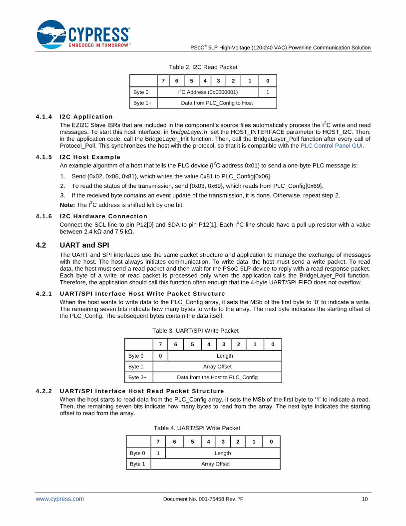
The EZI2C Slave ISRs that are included in the component’s source files automatically process the I2C write and read
messages. To start this host interface, in bridgeLayer.h, set the HOST_INTERFACE parameter to HOST_I2C. Then, in the application code, call the BridgeLayer_Init function. Then, call the BridgeLayer_Poll function after every call of Protocol_Poll. This synchronizes the host with the protocol, so that it is compatible with the PLC Control Panel GUI.
4.1.5 I2C Host Example
An example algorithm of a host that tells the PLC device (I2C address 0x01) to send a one-byte PLC message is:
1. Send 0x02, 0x06, 0x81, which writes the value 0x81 to PLC_Config[0x06].
2. To read the status of the transmission, send 0x03, 0x69, which reads from PLC_Config[0x69].
3. If the received byte contains an event update of the transmission, it is done. Otherwise, repeat step 2.
Note: The I2C address is shifted left by one bit.
4.1.6 I2C Hardware Connection
Connect the SCL line to pin P12[0] and SDA to pin P12[1]. Each I2C line should have a pull-up resistor with a value
between 2.4 kΩ and 7.5 kΩ.
4.2 UART and SPI
The UART and SPI interfaces use the same packet structure and application to manage the exchange of messages with the host. The host always initiates communication. To write data, the host must send a write packet. To read data, the host must send a read packet and then wait for the PSoC 5LP device to reply with a read response packet. Each byte of a write or read packet is processed only when the application calls the BridgeLayer_Poll function. Therefore, the application should call this function often enough that the 4-byte UART/SPI FIFO does not overflow.
4.2.1 UART/SPI In terface Host Wri te Pack et Structure
When the host wants to write data to the PLC_Config array, it sets the MSb of the first byte to ‘0’ to indicate a write. The remaining seven bits indicate how many bytes to write to the array. The next byte indicates the starting offset of the PLC_Config. The subsequent bytes contain the data itself.
Table 3. UART/SPI Write Packet
7 6 5 4 3 2 1 0
Byte 0 0 Length
Byte 1 Array Offset
Byte 2+ Data from the Host to PLC_Config
4.2.2 UART/SPI In terface Host Read Packet Structure
When the host starts to read data from the PLC_Config array, it sets the MSb of the first byte to ‘1’ to indicate a read. Then, the remaining seven bits indicate how many bytes to read from the array. The next byte indicates the starting offset to read from the array.
Table 4. UART/SPI Write Packet
7 6 5 4 3 2 1 0
Byte 0 1 Length
Byte 1 Array Offset

PSoC® 5LP High-Voltage (120-240 VAC) Powerline Communication Solution
www.cypress.com Document No. 001-76458 Rev. *F 11
4.2.3 UART/SPI In terface Read Response Packet Structure
After the PSoC 5LP device receives the read command, it responds with the requested data from the PLC_Config array. The Length parameter in the read packet sets the number of bytes to send.
Table 5. UART/SPI Interface Read Response Packet
7 6 5 4 3 2 1 0
Byte 0 Data from PLC_Config to the Host
4.2.4 UART/SPI Appl icat ion Flow
To start this host interface, in bridgeLayer.h, set the HOST_INTERFACE parameter to HOST_UART or HOST_SPI. Then, in the application code, call the BridgeLayer_Init function. The BridgeLayer_Poll function checks if the UART/SPI received a new byte or if the protocol must transmit a response. If it receives a new byte, it stores it according to the packet structure. If the packet is a read packet, it sets the variable hostByteTx to the length that is set by the read packet. If hostByteTx is greater than ‘0’ and UART/SPI FIFO is not full, it stores the next byte in the UART/SPI FIFO. If the protocol is in the middle of receiving a packet but does not receive a new byte in the time window set by the HOST_TIMEOUT parameter, the protocol resets the receiver to wait for a new message.
After an SPI master sends a read message, it should wait at least 1 ms before it starts to send the clock to read out the data, because the protocol requires time to load the response data into the FIFO.
5 External Hardware
Figure 8 shows the section of the hardware that interfaces the PSoC 5LP device to the powerline. With the appropriate coupling circuit, the PSoC 5LP PLC solution can operate on a wide range of powerline voltages and topologies. Attached to this application note are PCB design files for interfacing to the most common powerline high voltage range (120-240 VAC). The hardware contains the following:
PLC Device
Transmit Filter
Transmit Amplification
Receive Filter
Coupling Circuit

PSoC® 5LP High-Voltage (120-240 VAC) Powerline Communication Solution
www.cypress.com Document No. 001-76458 Rev. *F 12
Figure 8. PLC Hardware Interface Block Diagram
PSoC 5LP (CY8C56xx, CY8C58xx)
Programmable Digital and AnalogHost
Interface
(Optional)
Processing Core
32-bit ARM
Core
IRQ
64 KB
FLASH
16 KB
SRAM
DMA
ControllerI2C/
RS232/
SPI
GPIO Low Pass
Notch RC
Network
Low Pass
Notch RC
Network
fsk_out
fsk_in
AmplificationCoupling
Circuit
TX_Disable
PLC
Mode
Indicator
LEDs
Host
Interrupt
Po
we
rlin
e
Network
Protocol
FSK
Modulator
FSK
Demodulator RC
Filters /
Biasing
I-V Buffer

PSoC® 5LP High-Voltage (120-240 VAC) Powerline Communication Solution
www.cypress.com Document No. 001-76458 Rev. *F 13
5.1 PLC Device
This section includes the PSoC 5LP device as well as the bypass capacitors, and clock reference. Figure 20 shows the schematics while Table 6 lists the bill of materials (BOM).
Figure 9. PSoC 5LP PLC Device Related Schematics
Note: You can also implement the PLC solution on the 68-pin QFN package of the supported PSoC 5LP device.
To TX Filter or Amplifier
RX Filter
Opamp
To TX Amplifier
Correlator Output After DFB
filtering
TX I-V Buffer
From RX Filter
TX Filter Opamp
To Hysteresis Comparator

PSoC® 5LP High-Voltage (120-240 VAC) Powerline Communication Solution
www.cypress.com Document No. 001-76458 Rev. *F 14
Other than the decoupling capacitors, there are three key components:
Y3: The PSoC 5LP device uses a 24 MHz crystal to generate a precise 48 MHz bus clock for the FSK Modulator and FSK Demodulator. It is important that the ppm is low (≤30 ppm) to ensure high performance of the modem.
R67, C66 (Optional): These components are only necessary if the user wants to have a more sinusoidal FSK signal and wants to control the amplitude of the FSK signal in firmware. In the FSK Modulator component, set the Wave_Type parameter to Sine Wave. These components, along with a PSoC 5LP opamp, form a 150 kHz low-pass filter. This filter converts the IDAC’s current into a voltage and filters out the IDAC sampling noise. The output voltage is approximately the IDAC’s current multiplied by the value of R67. The IDAC range is 255 µA by default, but the sine wave values determine the actual maximum current. When R67 is 9.53 kΩ and the FSK_Amplitude_Divider is 3, the resulting peak-peak amplitude will be ~600 mVp-p. If the system requires the transmit filter, it is advisable to keep the amplitude to less than 2.0 Vp-p. To generate a clean signal, the board designer should place these components as close to the PSoC 5LP device as possible.
Note: The attached design files also have a 32.768 kHz crystal. This crystal is not necessary for the PLC circuit. It is only on the board for test purposes.
Table 6. PLC Device Related Bill of Materials
Description Designator Qty Value Manufacturer Manufacturer Part# VPN
Capacitor Ceramic 0.10 µF 10% 16 V X7R 0603
C40, C47, C48, C51, C52, C53, C55, C60, C67
9 0.1 µF TDK C1608X7R1C104K 445-1317-1-ND
Capacitor Ceramic 10 µF 20% 10 V X5R 0603
C44 1 10 µF TDK C1608X5R1A106M 445-6853-1-ND
Capacitor Ceramic 100 pF 5% 50 V NP0 0603
C66 1 100 pF TDK C1608C0G1H101J 445-1281-1-ND
Capacitor Ceramic 1.0 µF 16 V X7R 0603 C39, C43, C46, C54
4 1.0 µF TDK C1608X7R1C105K 445-1604-1-ND
Capacitor Ceramic 22 pF 100 V C0G 0603 C56, C57 2 22 pF Murata GRM1885C2A220JA01D 490-1335-1-ND
Resistor 9.53 k 1% 1/10 W 0603 R67 1 9.53 k Panasonic ERJ-3EKF9531V P9.53KHCT-ND
PSoC 5LP 32-bit µC 256 KB Flash 100-pin TQFP
U6 1 Cypress CY8C5868AXI-LP035
Crystal 24.000 MHz ±30 ppm 20 pF SMD Y3 1 24 MHz ECS Inc. ECS-240-20-5PX-TR XC1255CT-ND
5.2 Transmit Filter
The transmit filter circuit filters out the harmonics from the PLC device so that the signal on the line meets FCC part 15 and/or CENELEC EN50065-1 compliance standards. The PLC device uses FSK modulation to send the data on the powerline. To transmit logic ‘0’, the device generates a signal with frequency X (for example, 133 kHz) and to transmit logic ‘1’, the device generates a signal with frequency Y (for example, 130 kHz). However, the signal generated from the PLC device is not a pure sine wave. It contains harmonics, primarily at the third and fifth harmonics, as well as at the sampling frequency, which is approximately 8 times the FSK frequency. The FCC part 15 and CENELEC EN50065-1 standards have limits on the conducted emissions, which is the unintended “noise” emitted from the device. The transmit filter is necessary to reduce the harmonics below these limits. Figure 10 shows its location in the hardware architecture. The transmit filter is not necessary for systems that do not need to meet these standards. The filter does not provide any significant performance advantage, since the receiver filters out the harmonics before it demodulates the signal. To not use the transmit filter, connect the signal from the RC filter/I-V buffer directly to the transmit amplification stage.
PSoC® 5LP High-Voltage (120-240 VAC) Powerline Communication Solution
www.cypress.com Document No. 001-76458 Rev. *F 15
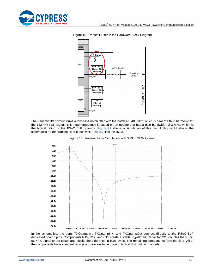
Figure 10. Transmit Filter in the Hardware Block Diagram
The transmit filter circuit forms a low-pass notch filter with the notch at ~400 kHz, which is near the third harmonic for the 132 kHz FSK signal. This notch frequency is based on an opamp that has a gain bandwidth of 3 MHz, which is the typical rating of the PSoC 5LP opamps. Figure 22 shows a simulation of this circuit. Figure 23 shows the schematics for the transmit filter circuit while Table 7 lists the BOM.
Figure 11. Transmit Filter Simulation with 3 MHz GBW Opamp
In the schematics, the ports TXOpampIn-, TXOpampIn+, and TXOpampOut connect directly to the PSoC 5LP dedicated opamp pins. Components R15, R17, and C15 create a stable VDDA/2 rail. Capacitor C23 couples the PSoC 5LP TX signal to the circuit and blocks the difference in bias levels. The remaining components form the filter. All of the components have standard ratings and are available through typical distribution channels.
PSoC 5LP (CY8C56xx, CY8C58xx)
Programmable Digital and AnalogHost
Interface
(Optional)
Processing Core
32-bit ARM
Core
IRQ
64 KB
FLASH
16 KB
SRAM
DMA
ControllerI2C/
RS232/
SPI
GPIO Low Pass
Notch RC
Network
Low Pass
Notch RC
Network
fsk_out
fsk_in
AmplificationCoupling
Circuit
TX_Disable
PLC
Mode
Indicator
LEDs
Host
Interrupt
Po
we
rlin
e
Network
Protocol
FSK
Modulator
FSK
Demodulator RC
Filters /
Biasing
I-V Buffer

PSoC® 5LP High-Voltage (120-240 VAC) Powerline Communication Solution
www.cypress.com Document No. 001-76458 Rev. *F 16
In terms of the layout, the board designer should place the feedback components R21, R19, C20, and C22 as close to the opamp pins as possible.
Note: The attached design files also have an external opamp U2 in the transmit filter circuit. This opamp is not necessary for the PLC circuit. It is only on the board for test purposes.
Figure 12. Transmit Filter Schematics
Table 7. Transmit Filter Bill of Materials
Description Designator Qty Value Manufacturer Manufacturer Part# VPN
Capacitor Ceramic 470 pF 5% 50 V C0G 0603
C20, C22 2 470 pF Murata GRM1885C1H471JA01D 490-1443-1-ND
Capacitor Ceramic 1.0 µF 16 V X7R 0603
C15, C23 2 1.0 µF TDK C1608X7R1C105K 445-1604-1-ND
Resistor 10.0 k 1% 1/10 W 0603
R15, R17 2 10.0 k Yageo RC0603FR-0710KL 311-10.0KHRCT-ND
Resistor 4.99 k 1% 1/10 W 0603
R19 1 4.99 k Panasonic ERJ-3EKF4991V P4.99KHCT-ND
Resistor 1.10 k 1% 1/10 W 0603
R20 1 1.10 k Panasonic ERJ-3EKF1101V P1.10KHCT-ND
Resistor 1.87 k 1% 1/10 W 0603
R21 1 1.87 k Panasonic ERJ-3EKF1871V P1.87KHCT-ND
Resistor 1.69 k 1% 1/10 W 0603
R22 1 1.69 k Panasonic ERJ-3EKF1691V P1.69KHCT-ND
Resistor 976 1% 1/10 W 0603
R26 1 976 Panasonic ERJ-3EKF9760V P976HCT-ND
Resistor 909 1% 1/10 W 0603
R27 1 909 Panasonic ERJ-3EKF9090V P909HCT-ND
Resistor 182 1% 1/10 W 0603
R33 1 182 Panasonic ERJ-3EKF1820V P182HCT-ND
To TX Amplifier
From TX I-V Buffer

PSoC® 5LP High-Voltage (120-240 VAC) Powerline Communication Solution
www.cypress.com Document No. 001-76458 Rev. *F 17
PSoC 5LP (CY8C56xx, CY8C58xx)
Programmable Digital and AnalogHost
Interface
(Optional)
Processing Core
32-bit ARM
Core
IRQ
64 KB
FLASH
16 KB
SRAM
DMA
ControllerI2C/
RS232/
SPI
GPIO Low Pass
Notch RC
Network
Low Pass
Notch RC
Network
fsk_out
fsk_in
AmplificationCoupling
Circuit
TX_Disable
PLC
Mode
Indicator
LEDs
Host
Interrupt
Po
we
rlin
e
Network
Protocol
FSK
Modulator
FSK
Demodulator RC
Filters /
Biasing
I-V Buffer
5.3 Transmit Amplification
The transmit amplification circuit boosts the PLC signal’s voltage and current to drive the signal on the powerline. This is necessary because the load impedance on the powerline is often unknown and can be lower than 1 ohm. Additionally, it helps drive the signal over long distances. Figure 13 shows its location in the hardware architecture.
Figure 13. Transmit Amplification in the Hardware Block Diagram
shows the schematic for the transmit amplification circuit while Table 8 lists the BOM. If the FSK Modulator
component’s Wave_Type parameter is Sine_Wave and the Transmit_Filter parameter is Enabled, then the input signal will come from the Transmit Filter circuit. If the Wave_Type parameter is Sine_Wave and the Transmit_Filter parameter is Disabled, then the input signal will come from the TX I-V Buffer circuit. If the Wave_Type parameter is Square_Wave, then the input signal will come directly from a PSoC 5LP digital output pin.
The recommended power rail (VPWR) should be greater than the desired signal amplitude and less than the maximum rating of the opamp U4. To meet the FCC part 15 and/or CENELEC EN50065-1 standards, the VPWR rail should be 10 to 12 V.
PSoC® 5LP High-Voltage (120-240 VAC) Powerline Communication Solution
www.cypress.com Document No. 001-76458 Rev. *F 18
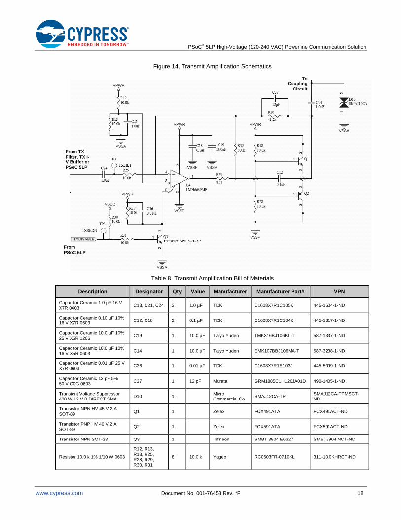
Figure 14. Transmit Amplification Schematics
Table 8. Transmit Amplification Bill of Materials
Description Designator Qty Value Manufacturer Manufacturer Part# VPN
Capacitor Ceramic 1.0 µF 16 V X7R 0603
C13, C21, C24 3 1.0 µF TDK C1608X7R1C105K 445-1604-1-ND
Capacitor Ceramic 0.10 µF 10% 16 V X7R 0603
C12, C18 2 0.1 µF TDK C1608X7R1C104K 445-1317-1-ND
Capacitor Ceramic 10.0 µF 10% 25 V X5R 1206
C19 1 10.0 µF Taiyo Yuden TMK316BJ106KL-T 587-1337-1-ND
Capacitor Ceramic 10.0 µF 10% 16 V X5R 0603
C14 1 10.0 µF Taiyo Yuden EMK107BBJ106MA-T 587-3238-1-ND
Capacitor Ceramic 0.01 µF 25 V X7R 0603
C36 1 0.01 µF TDK C1608X7R1E103J 445-5099-1-ND
Capacitor Ceramic 12 pF 5% 50 V C0G 0603
C37 1 12 pF Murata GRM1885C1H120JA01D 490-1405-1-ND
Transient Voltage Suppressor 400 W 12 V BIDIRECT SMA
D10 1 Micro Commercial Co
SMAJ12CA-TP SMAJ12CA-TPMSCT-ND
Transistor NPN HV 45 V 2 A SOT-89
Q1 1 Zetex FCX491ATA FCX491ACT-ND
Transistor PNP HV 40 V 2 A SOT-89
Q2 1 Zetex FCX591ATA FCX591ACT-ND
Transistor NPN SOT-23 Q3 1 Infineon SMBT 3904 E6327 SMBT3904INCT-ND
Resistor 10.0 k 1% 1/10 W 0603
R12, R13, R18, R25, R28, R29, R30, R31
8 10.0 k Yageo RC0603FR-0710KL 311-10.0KHRCT-ND
To Coupling
Circuit
From
PSoC 5LP
From TX Filter, TX I-V Buffer,or PSoC 5LP

PSoC® 5LP High-Voltage (120-240 VAC) Powerline Communication Solution
www.cypress.com Document No. 001-76458 Rev. *F 19
Description Designator Qty Value Manufacturer Manufacturer Part# VPN
Resistor 41.2 k 1% 1/10 W 0603 R16 1 41.2 k Yageo RRC0603FR-0741K2L 311-41.2KHRCT-ND
Resistor 3.01 1% 1/10 W 0603 R23 1 3.01 Yageo RC0603FR-073R01L 311-3.01HRCT-ND
Resistor 300 k 1% 1/10 W 0603 R32 1 300 k Panasonic ERJ-3EKF3003V P300KHCT-ND
Op-Amp 190 MHz U4 1 National Semiconductor
LMH6639MF/NOPB LMH6639MFCT-ND
Components R12, R13, and C21 form the VPWR/2 rail that biases opamp U4. Components R30, R31, Q3, R29, and C36 convert the PSoC 5LP’s TX_Disable signal from a VDD rail to a VPWR rail so that the FSK Modulator can disable the opamp U4 when it is not transmitting. The capacitor C24 couples the output of the transmit filter (or the PSoC 5LP directly if the FSK Modulator’s Wave_Type is Square Wave). Resistors R25 and R32 form the gain for the opamp, while R25 and R16 form the gain for the entire stage, which is more important. The gain is set to ~4x (12 dB) to boost the amplitude from the transmit filter. Capacitor C37 removes any high frequency ringing in the feedback path. Capacitors C18 and C19 decouple the noise from the power. Resistor R23 limits the current of the U4 output. R18 and R28 bias the transistors Q1 and Q2 so that they turn off when U4 is disabled. Capacitor C12 reduces high frequency ringing. Transistors Q1 and Q2 are high-current (2A) transistors that can drive low-impedance loads. Capacitor C14 couples the transmit path to the coupling and prevents the transformer or inductor from DC shorting the transmitter. Diode D10 is for surge protection.
The opamp U4 is a critical component, because it controls the high-current transistors. The opamp must meet these requirements:
Rail-to-rail output drive capability ≥100 mA
Gain bandwidth product (GBW) >50 MHz
Voltage feedback
The maximum VDD - VSS rating of the opamp should be greater than the VPWR rail and the required signal amplitude. VDD - VSS is ≥10 V when FCC or CENELEC compliance is required.
Power supply rejection ratio (PSRR) >70 dB
Total harmonic distortion (THD) < – 60 dB
Includes a shutdown pin to turn off its output when not transmitting PLC data. This ensures a high impedance so that the transmitter does not attenuate the received signal. The current requirement is typically <1 mA to drive the shutdown pin.
In the schematics, there are two ground rails: VSSA (Analog) and VSSP (Power). These rails must connect together at a point but be separate otherwise. This placement minimizes the large switching noise of the transistors and reduces disruption of the sensitive analog signal paths of the transmitter and receiver.
Note: The attached design files also have a second opamp U9 in the transmit amplification circuit. This opamp is not necessary for the PLC circuit. It is only on the board for test purposes.
PSoC® 5LP High-Voltage (120-240 VAC) Powerline Communication Solution
www.cypress.com Document No. 001-76458 Rev. *F 20
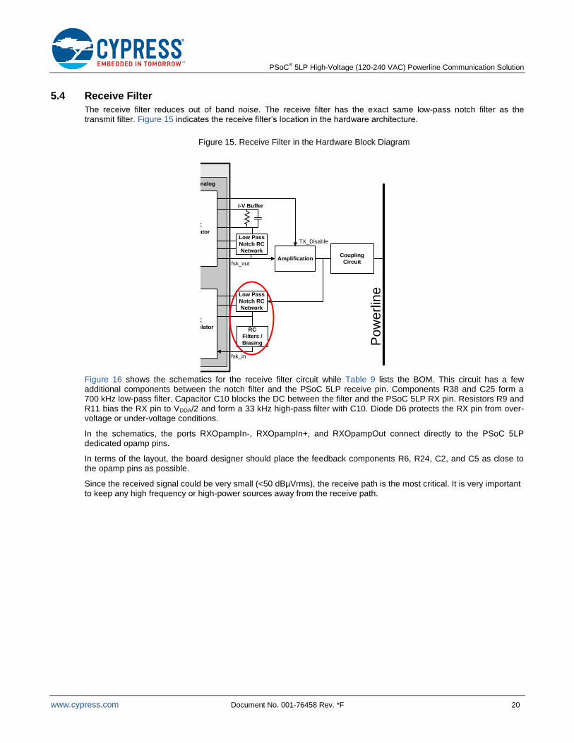
5.4 Receive Filter
The receive filter reduces out of band noise. The receive filter has the exact same low-pass notch filter as the transmit filter. Figure 15 indicates the receive filter’s location in the hardware architecture.
Figure 15. Receive Filter in the Hardware Block Diagram
Figure 16 shows the schematics for the receive filter circuit while Table 9 lists the BOM. This circuit has a few additional components between the notch filter and the PSoC 5LP receive pin. Components R38 and C25 form a 700 kHz low-pass filter. Capacitor C10 blocks the DC between the filter and the PSoC 5LP RX pin. Resistors R9 and R11 bias the RX pin to VDDA/2 and form a 33 kHz high-pass filter with C10. Diode D6 protects the RX pin from over-voltage or under-voltage conditions.
In the schematics, the ports RXOpampIn-, RXOpampIn+, and RXOpampOut connect directly to the PSoC 5LP dedicated opamp pins.
In terms of the layout, the board designer should place the feedback components R6, R24, C2, and C5 as close to the opamp pins as possible.
Since the received signal could be very small (<50 dBµVrms), the receive path is the most critical. It is very important to keep any high frequency or high-power sources away from the receive path.
PSoC 5LP (CY8C56xx, CY8C58xx)
Programmable Digital and AnalogHost
Interface
(Optional)
Processing Core
32-bit ARM
Core
IRQ
64 KB
FLASH
16 KB
SRAM
DMA
ControllerI2C/
RS232/
SPI
GPIO Low Pass
Notch RC
Network
Low Pass
Notch RC
Network
fsk_out
fsk_in
AmplificationCoupling
Circuit
TX_Disable
PLC
Mode
Indicator
LEDs
Host
Interrupt
Po
we
rlin
e
Network
Protocol
FSK
Modulator
FSK
Demodulator RC
Filters /
Biasing
I-V Buffer

PSoC® 5LP High-Voltage (120-240 VAC) Powerline Communication Solution
www.cypress.com Document No. 001-76458 Rev. *F 21
Figure 16. Receive Filter Schematics
Table 9. Receive Filter Bill of Materials
Description Designator Qty Value Manufacturer Manufacturer Part# VPN
Capacitor Ceramic 1.0 µF 16V X7R 0603
C1 1 1.0 µF TDK C1608X7R1C105K 445-1604-1-ND
Capacitor Ceramic 470 pF 5% 50V C0G 0603
C2, C5, C10, C25
4 470 pF Murata GRM1885C1H471JA01D
490-1443-1-ND
Capacitor Ceramic 0.10 µF 10% 16V X7R 0603
C17 1 0.1 µF TDK C1608X7R1C104K 445-1317-1-ND
Dual Schottky Diode D6 1 ST Micro BAT54SFILM 497-2522-1-ND
Resistor 10.0 k 1% 1/10 W 0603 R1, R3 2 10.0 k Yageo RC0603FR-0710KL 311-10.0KHRCT-ND
Resistor 4.99 k 1% 1/10 W 0603 R6 1 4.99 k Panasonic ERJ-3EKF4991V P4.99KHCT-ND
Resistor 1.10 k 1% 1/10 W 0603 R7 1 1.10 k Panasonic ERJ-3EKF1101V P1.10KHCT-ND
Resistor 1.87 k 1% 1/10 W 0603 R24 1 1.87 k Panasonic ERJ-3EKF1871V P1.87KHCT-ND
Resistor 1.69 k 1% 1/10 W 0603 R8 1 1.69 k Panasonic ERJ-3EKF1691V P1.69KHCT-ND
Resistor 976 1% 1/10 W 0603 R4 1 976 Panasonic ERJ-3EKF9760V P976HCT-ND
Resistor 909 1% 1/10 W 0603 R37 1 909 Panasonic ERJ-3EKF9090V P909HCT-ND
Resistor 182 1% 1/10 W 0603 R34 1 182 Panasonic ERJ-3EKF1820V P182HCT-ND
Resistor 499 1% 1/10 W 0603 R38 1 499 Panasonic ERJ-3EKF4990V P499HCT-ND
Resistor 20.0 k 1% 1/10 W 0603 R9, R11 2 20.0 k Yageo RC0603FR-0720KL 311-20.0KHRCT-ND
5.5 Coupling Circuit
The coupling circuit provides a low impedance path for the PLC signal between the powerline and the PLC transmit/receive circuitry and blocks the power from destroying the low-voltage components. Line-Neutral (L-N) coupling is the most common coupling scheme for high-voltage AC PLC systems. It is most common because neutral is always present. There are European leakage current restrictions on using earth to couple the signal, and line-earth coupling can have problems with low-current ground fault interrupters (GFI). An isolated design helps to avoid potential electric shock hazards for applications that require direct user interface.
From Coupling
Circuit
To
PSoC 5LP
RX
PSoC® 5LP High-Voltage (120-240 VAC) Powerline Communication Solution
www.cypress.com Document No. 001-76458 Rev. *F 22
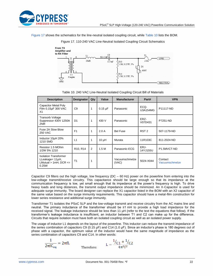
Figure 17 shows the schematics for the line-neutral isolated coupling circuit, while Table 10 lists the BOM.
Figure 17. 110-240 VAC Line-Neutral Isolated Coupling Circuit Schematics
Table 10. 240 VAC Line-Neutral Isolated Coupling Circuit Bill of Materials
Description Designator Qty Value Manufacturer Part# VPN
Capacitor Metal Poly Film 0.15µF 300 VAC X1
C9 1 0.15 µF Panasonic ECQ-U3A154MG
P11117-ND
Transorb Voltage Suppressor 430V 1250A ZNR
D1 1 430 V Panasonic ERZ-V07D431
P7251-ND
Fuse 2A Slow Blow 250 VAC
F1 1 2.0 A Bel Fuse RST 2 507-1179-ND
Inductor 10µH 20% 1210 SMD
L1 1 10 µH Murata 11R103C 811-2024-ND
Resistor 1.5 MOhm 1/2W 5% 1210
R10, R14 2 1.5 M Panasonic-ECG ERJ-14YJ155U
P1.5MVCT-ND
Isolation Transformer LLeakage< 11µH, LMutual > 1mH, DCR <= 0.25W
T1 1 Vacuumschmelze (VAC)
5024-X044 Contact Vacuumschmelze
Capacitor C9 filters out the high voltage, low frequency (DC – 60 Hz) power on the powerline from entering into the low-voltage transmit/receive circuitry. This capacitance should be large enough so that its impedance at the communication frequency is low, yet small enough that its impedance at the power’s frequency is high. To drive heavy loads and long distances, the transmit output impedance should be minimized. An X-Capacitor is used for adequate surge immunity. The board designer can replace the X1 capacitor listed in the BOM with an X2 capacitor of the same value based on the surge immunity requirements. This capacitor should have a metal-film construction for lower series resistance and additional surge immunity.
Transformer T1 isolates the PSoC 5LP and the low-voltage transmit and receive circuitry from the AC mains line and neutral. The primary inductance of the transformer should be ≥1 mH to provide a high load impedance for the received signal. The leakage inductance should be less than 11 µH (refer to the text the equations that follow). If the transformer’s leakage inductance is insufficient, an inductor between T1 and C2 can make up for the difference. Circuits that require isolation must have both an isolated coupling circuit as well as an isolated power supply.
The usage of inductor L1 depends on the layout of the powerline. This inductor can reduce the transmit impedance of the series combination of capacitors C9 (0.15 µF) and C14 (1.0 µF). Since an inductor’s phase is 180 degrees out of phase with a capacitor, the optimum value of the inductor would have the same magnitude of impedance as the series combination of capacitors C9 and C14. In other words:
Therefore:
From TX Amplifier and to RX Filter

PSoC® 5LP High-Voltage (120-240 VAC) Powerline Communication Solution
www.cypress.com Document No. 001-76458 Rev. *F 23
Substituting f = 132 kHz, C1 = 1 µF, C2 = 0.15 µF yields: L = 11.1 H
Since the leakage inductance of transformer T1 is 1 µH, the ideal value for L1 is 10 µH. Since impedance includes
both resistance and reactance, the inductor’s DC resistance should be less than 0.25 to minimize resistive attenuation. To drive heavy loads, the inductor’s current rating should be greater than 700 mA. Since the powerline cable has its own series inductance (in addition to a DC resistance and load capacitance), this inductance has the
same effect as with L1. If the inductance is greater than 11 H, it over-compensates for capacitor C2 and starts to
cause attenuation of the signal. Therefore, it is optimal that L1 be less than (11 H – Lcable). The specification for
inductance of a powerline cable is usually given in H/ft, and it is typically between 0.1 and 0.25 H/ft. A 60 ft cable
with average inductance (0.18 H/ft) has ~11 H of total inductance. Therefore, inductor L1 is only advisable if the distance between nodes is less than 60 ft.
Resistors R10 and R14 discharges capacitor C9 when power is removed from the system. R10 and R4 are sometimes known as bleeder resistors. In some systems, the on-board power supply is able to discharge the capacitor quickly enough, such that these resistors are not necessary.
Diode D1 provides greater surge immunity. The board designer can replace this component with two back-to-back zener diodes (for example, with two 5 Watt Zener diodes with the same part number IN5343B (Digikey#1N5343BMSCT-ND)).
The board designer should follow the proper high voltage safety guidelines (e.g. EN60950).
Power Supply Design Considerations
In addition to the overall system requirements, the power supply must meet the following requirements:
Provide a VPWR rail (up to 12 V for the opamp U4 in Figure 13) for the transmit amplification circuit. The amount of current is based on how much loading is on the line. For typical AC powerlines, a 150
mA rating is
recommended.
Provide a 5 V VDD rail that supplies >100 mA of current for the PSoC 5LP device.
If the system uses a switch-mode power supply, select a switching frequency such that the fundamental frequency and harmonics are not within ±5 kHz of the PLC frequencies. For example, for the 130 to 133 kHz PLC frequencies, avoid switching frequencies of 42 to 46 kHz, 63 to 69 kHz, and 125 to 138 kHz. This provides the best receiver input sensitivity.
Many power supplies use large bulk capacitors (>1 µF) across line and neutral for EMI reduction (C30 and C31
in Figure 18). These capacitors attenuates the PLC signal, because at 130 kHz, they have an impedance <1.2 . To prevent this, place an inductor (L3 in the schematics) between the line and these capacitors. The value of the
inductor will be a large factor in the receiver’s impedance. A high impedance (>500 ) is necessary if there are long transmission distances (>1 km) or if there are many (>500) PLC nodes on the network. A 1.5 mH inductor
provides an impedance of 1240 at 130 kHz.
Figure 18. Power Supply Line Filtering Schematics

PSoC® 5LP High-Voltage (120-240 VAC) Powerline Communication Solution
www.cypress.com Document No. 001-76458 Rev. *F 24
Table 11. Power Supply Line Filter Bill of Materials
Description Designator Qty Value Manufacturer Manufacturer Part# VPN
Capacitor Metal Poly Film 0.022uF 300 VAC X1
C29 1 0.022 µF Panasonic ECQ-U3A223MG P11112-ND
Inductor 1500uH 0.2A 10% Radial
L3 1 1.5 mH TDK TSL0808RA-152KR21-PF 445-3757-1-ND
The power supply in the attached design files provides a low-cost solution that meets these requirements. However, as it does not regulate the load, the supply voltage drops with increased current (by approximately -25 mV per 1 mA increase). The board consumes ~100 mA when there is a heavy load (1 F capacitor) on the line. In this case, the supply voltage drops to ~7.0 V, which stills work for this system. However, for systems that require tighter load regulation or have higher current consumption, the designer should select a different supply or add load regulation.
6 Performance
This section provides the typical performance of the PSoC 5LP PLC solution, which uses the attached code example as the firmware and the attached design files as the hardware except where noted.
6.1 Transmitter Conducted Emissions
For systems that must comply with FCC Part 15 or CENELEC EN50065-1, the transmitter’s output signal must be below specified limits. Figure 19 shows the conducted emissions test setup. A line impedance stabilization network
(LISN) provides a stable 50 impedance, and we use it for CENELEC compliance tests. A spectrum analyzer
connects to the 50 monitor of the LISN. We modified the PSoC 5LP PLC firmware so that the transmitter constantly transmits a PLC signal that switches between 130.4 kHz and 133.3 kHz and the FSK_Amplitude_Divider parameter is 3.
Figure 19. Conducted Emissions Test Setup
PSoC 5LP PLC
Test Board
EMCO 3810/2
LISN
Agilent E4411B
Spectrum
Analyzer
Line
50 Ohm monitor
120V/60Hz AC Powerline
Neutral
Line Neutral
Figure 31 shows the test results of the PLC transmitter. The red line is the limit for CENELEC and FCC. The FCC specification only covers the frequencies above 150 kHz. The CENELEC specification also defines limits for frequencies 3 kHz to 150 kHz and the maximum PLC signal limit of 122 dBµVrms at the carrier frequency. The Cypress PLC transmitter’s emissions have at least a 5 dB margin to the specification limits.

PSoC® 5LP High-Voltage (120-240 VAC) Powerline Communication Solution
www.cypress.com Document No. 001-76458 Rev. *F 25
Figure 20. Conducted Emissions at 132 kHz
6.2 Transmission with Heavy Loads
Typical residential powerlines have impedances that vary between 3 and 50 . In most situations, the transmitter can drive these loads, especially over long distances. Figure 32 shows the setup for this test. The test equipment is the same as the conducted emissions test with the variation of the following parameters:
The cable between the test board and LISN is 3, 50, or 100 ft. The cable gauge is 16 AWG.
The load is either the 50 impedance of the LISN or a 1 F capacitor (1.2 impedance @ 130 kHz). The
capacitor is X1 safety rated and rated for 250 VAC powerlines. There is also a 1 M resistor, which is used to discharge the capacitor when it is removed from the powerline. This bleeds out the voltage, so that it does not shock the person that handles it
Figure 21. Transmitter Loading Test Setup
PSoC 5LP PLC
Test Board
EMCO 3810/2
LISN
Agilent E4411B
Spectrum
Analyzer
50 Ohm
120V AC Powerline
Neutral
Line Neutral
1 MOhm1uF
3 ft / 50 ft /
100 ft
Cable
Line
On the PSoC 5LP PLC test board, the inductor L1 is either the default 10 mH inductor, or it is shorted out. See the Coupling Circuit section for details on how to select the L1.
0
120
Am
plitu
de
(d
B
V)
CENELEC Max PLC
Signal Limit = 122 dBV
CENELEC and FCC
Emissions Limit
2021

PSoC® 5LP High-Voltage (120-240 VAC) Powerline Communication Solution
www.cypress.com Document No. 001-76458 Rev. *F 26
Figure 22 shows the test results. When the load impedance decreases, the amplitude of the signal decreases, as expected. However, even with a worst-case load, the signal level is still sufficiently above the minimum sensitivity (see the Receiver Input Sensitivity section for details).
Figure 22. Transmitter Loading Test Results
As described in the Coupling Circuit section, the inductor matches the impedance of the capacitor, so the transmit impedance is as low as possible at the output of the test board as demonstrated by the increased amplitude at 3 ft for the green line as compared with the red line. However, for longer cable lengths, the inductance of the cable causes the total inductance to be greater than the capacitance, which increases the transmit impedance. This explains why the green line continuously decreases with cable length. Conversely, when an inductor is not used, the impedance at the test board is more capacitive. As the cable length increases, the additional inductance offsets the capacitance as demonstrated by the red line, where the amplitude actually increases as the cable increases from 3 to 50 ft.
Therefore, the use of the inductor depends on how much cable is between the transmitter and the loads on the
powerline. For cable lengths less than 30 ft, a 10 H inductor helps to increase the amplitude. Otherwise, an inductor is not necessary.
6.3 Receiver Input Sensitivity
The receiver sensitivity determines the minimum amplitude that the receiver can successfully receive PLC data. Cable length, loading (televisions, switching power supplies, motors, and so on), and any components that are in the path (circuit breakers, transformers) can affect the amplitude of the PLC signal.
Figure 23 shows the setup for the receiver sensitivity test. A PSoC 5LP PLC test board transmits PLC packets (8-byte header) to a second PSoC 5LP PLC board. A spectrum analyzer measures the received signal at the input to the receiver filter (C4, on the left side of Figure 16).
Amplitude vs Cable Length with
Various Loads
90
95
100
105
110
115
120
0 20 40 60 80 100 120
Cable Length (ft)
Am
pli
tud
e (
dB
uV
)
1uF Load, L1 = Short
1uF Load, L1 = 10uH
50 Ohm Load, L1 = Short or 10uH

PSoC® 5LP High-Voltage (120-240 VAC) Powerline Communication Solution
www.cypress.com Document No. 001-76458 Rev. *F 27
Figure 23. Receiver Sensitivity Test Setup
PSoC 5LP PLC
Test Board
(Transmitting)
Opamp Disabled
EMCO 3810/2
LISN
120V AC Powerline
PSoC 5 PLC Test
Board (Receiving)
100 feet
Agilent E4411B
Spectrum Analyzer
FSK Test Point
Referring to the transmit amplification circuit in Figure 13, we disconnect power to the amplification circuit (VPWR),
which means that the filtered transmit signal passes through R25 (10.0 k ) and R16 (41.2 k) resulting in a very
high impedance. On the receiving board, the spectrum analyzer provides a 50 load, which causes the signal to be heavily attenuated. The TX_GAIN byte in the PLC_Config array sets the amplitude of the signal.
The transmitter sends at least 1000 packets and the receiver displays how many packets were successfully received (valid CRC). The following formula converts the packet success rate (PSR) to a bit error rate:
Where the PacketLength = 80 (10 bytes × 8 bits)
A BER of 10-3
is equivalent to an approximately 92 percent success rate for this packet length. A BER of 10-4
is equivalent to an approximately 99 percent success rate.
Figure 24 shows the receiver sensitivity test results for the 132 kHz FSK center frequency and for four different
receive gain values. The noise floor was ~20 dBV. The results show that the system can successfully receive a 43 dBµVrms signal with a BER less than 10
-3 and a 45 dBµVrms signal with a BER less than 10
-4. When the system
transmits at the CENELEC compliant level of 122 dBµVrms, this means that the signal can be attenuated by 77 dB (7000x).
When the receive gain is increased from 1x to 2x, the input sensitivity is improved by 1-2 dB (that is, the device can receive a 1-2 dB smaller signal). When the receive gain is increased from 2x to 4x, the input sensitivity is improved by 1-2 dB when the input amplitude is less than 45 dBµVrms. However, at amplitudes greater than 45 dBµVrms, the input sensitivity is approximately the same as when the receive gain is 2x. The Narrow-band SNR section shows the tradeoff for increasing the receive gain.
Figure 25 shows results for the 110 kHz FSK center frequency. The results show that the system can successfully receive a 43 dBµVrms signal with a BER less than 10
-3 and a 46 dBµVrms signal with a BER less than 10
-4.

PSoC® 5LP High-Voltage (120-240 VAC) Powerline Communication Solution
www.cypress.com Document No. 001-76458 Rev. *F 28
Figure 24. Receiver Sensitivity Test Results at 132 kHz FSK Center Frequency with Different Receive Gains
Figure 25. Receiver Sensitivity Test Results at 110 kHz FSK Center Frequency with Different Receive Gains
Figure 26 (132 kHz FSK) and Figure 27 (110 kHz FSK) show the receiver input sensitivity test results when FEC encoding and frequency hopping are each enabled. With the frequency hopping option, the transmitter continuously sends packets with a fixed FSK center frequency while the receiver hops between 110 kHz and 132 kHz until it detects the FSK signal for each packet. Since the receiver stays locked on the FSK center frequency for 500 ms after it receives a valid packet (default value of Frequency_Hopping_Lock_Time), the transmitter in this test waits for 600 ms between transmitting packets so that the receiver doesn’t stay locked and goes back to frequency hopping. This tests the receiver’s ability to find the correct frequency for each packet. It normal applications, the receiver will stay locked on that frequency until after the following packet is transmitted.
1.00E-06
1.00E-05
1.00E-04
1.00E-03
1.00E-02
1.00E-01
1.00E+00
37 38 39 40 41 42 43 44 45 46 47 48 49
BE
R
Input Amplitude (dBuVrms)
Bit Error Rate (BER) vs. Input Amplitude for 132 kHz FSK
RxGain = 1x
RxGain = 2x
RxGain = 4x
RxGain = 8x
1.00E-06
1.00E-05
1.00E-04
1.00E-03
1.00E-02
1.00E-01
1.00E+00
36 37 38 39 40 41 42 43 44 45 46 47 48 49 50 51 52
BE
R
Input Amplitude (dBuVrms)
Bit Error Rate (BER) vs. Input Amplitude for 110 kHz FSK
RxGain = 1x
RxGain = 2x
RxGain = 4x
RxGain = 8x
PSoC® 5LP High-Voltage (120-240 VAC) Powerline Communication Solution
www.cypress.com Document No. 001-76458 Rev. *F 29
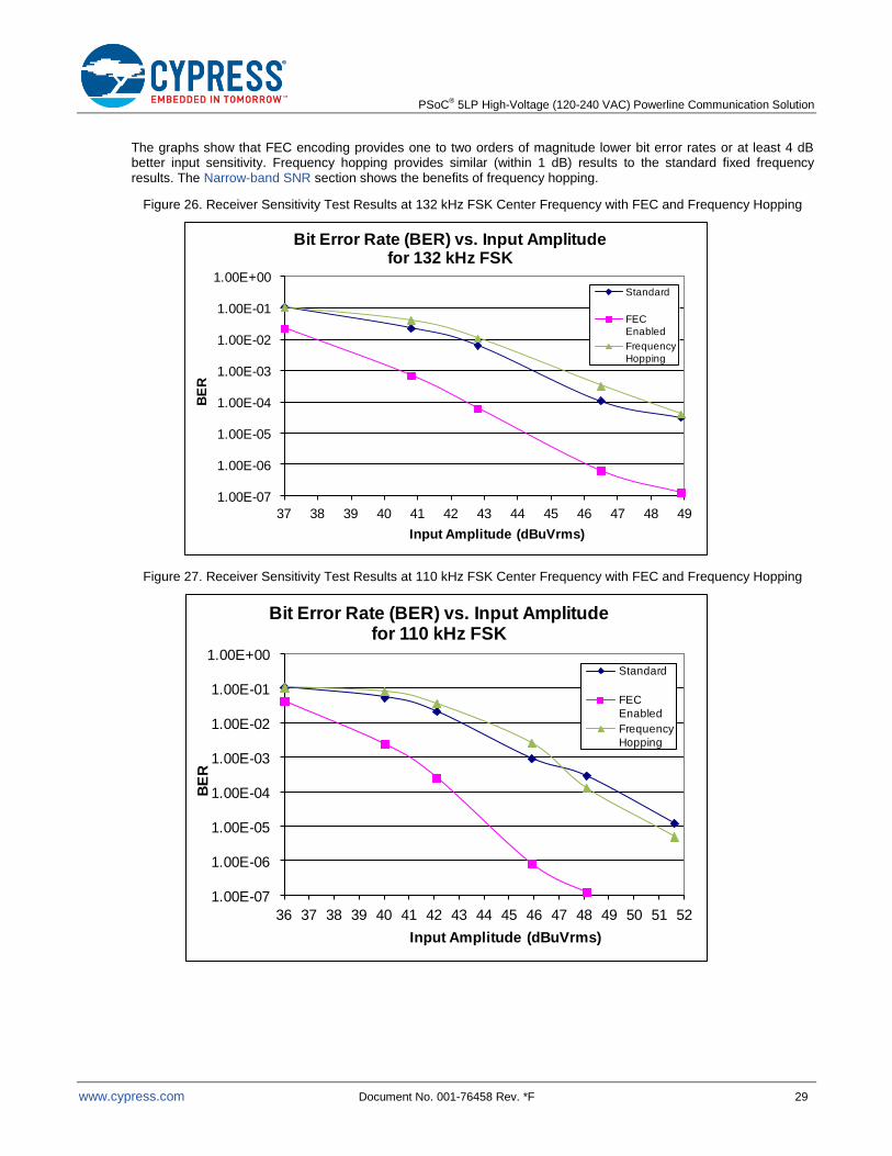
The graphs show that FEC encoding provides one to two orders of magnitude lower bit error rates or at least 4 dB better input sensitivity. Frequency hopping provides similar (within 1 dB) results to the standard fixed frequency results. The Narrow-band SNR section shows the benefits of frequency hopping.
Figure 26. Receiver Sensitivity Test Results at 132 kHz FSK Center Frequency with FEC and Frequency Hopping
Figure 27. Receiver Sensitivity Test Results at 110 kHz FSK Center Frequency with FEC and Frequency Hopping
1.00E-07
1.00E-06
1.00E-05
1.00E-04
1.00E-03
1.00E-02
1.00E-01
1.00E+00
37 38 39 40 41 42 43 44 45 46 47 48 49
BE
R
Input Amplitude (dBuVrms)
Bit Error Rate (BER) vs. Input Amplitude for 132 kHz FSK
Standard
FEC
Enabled
Frequency
Hopping
1.00E-07
1.00E-06
1.00E-05
1.00E-04
1.00E-03
1.00E-02
1.00E-01
1.00E+00
36 37 38 39 40 41 42 43 44 45 46 47 48 49 50 51 52
BE
R
Input Amplitude (dBuVrms)
Bit Error Rate (BER) vs. Input Amplitude for 110 kHz FSK
Standard
FEC
Enabled
Frequency
Hopping

PSoC® 5LP High-Voltage (120-240 VAC) Powerline Communication Solution
www.cypress.com Document No. 001-76458 Rev. *F 30
6.4 Receiver Noise Immunity
The packet transmission success rate in the presence of noise on the powerline determines the noise immunity of the receiver. Examples of noise sources are televisions, vacuums, and intercoms. Figure 28 shows the receiver noise test setup. As in the receiver sensitivity test, the transmitter sends at least 1000 packets for each test, and we measure the percentage of packets received. The spectrum analyzer measures the input to the receive filter. The
TX_Amplitude_Divider parameter is 192, so that the transmitter generates an amplitude of 86 dBV at the receiver filter input.
Figure 28. Receiver Noise Immunity Test Setup
Transmit
Amplification and
Coupling Circuit
EMCO 3810/2
LISN
120V AC Powerline
PSoC 5 PLC Test
Board (Receiving)
6 feet
Agilent E4411B
Spectrum Analyzer
FSK Test Point
PSoC 5LP PLC
Test Board
(Transmitting)
Opamp Disabled
Agilent 33250
Waveform
Generator
6.4.1 White Noise SNR
For this test, the waveform generator is set to Noise mode. We vary the amplitude of the noise and measure the packet success rate. The bit error rate (BER) calculation is the same as the receiver sensitivity test. To calculate the signal-noise ratio (SNR), subtract the noise level from the PLC signal.
Figure 29 shows the results of the white noise test at 132 kHz FSK center frequency. As the noise level increases, the SNR decreases and the BER increases. The BER is less than 10
-3 for an SNR greater than 10 dB. The BER is
less than 10-4
for an SNR greater than 11 dB. There is less than 1 dB difference between the results of the different receive gain values.
Figure 30 shows the results of the white noise test at 110 kHz FSK center frequency. The BER is less than 10-3
for an SNR greater than 7 dB. The BER is less than 10
-4 for an SNR greater than 9 dB. There is less than 1 dB difference
between the results of the different receive gain values.
PSoC® 5LP High-Voltage (120-240 VAC) Powerline Communication Solution
www.cypress.com Document No. 001-76458 Rev. *F 31
Figure 29. Receiver White Noise Immunity Test Results at 132 kHz with Different Receive Gains
Figure 30. Receiver White Noise Immunity Test Results at 110 kHz with Different Receive Gains
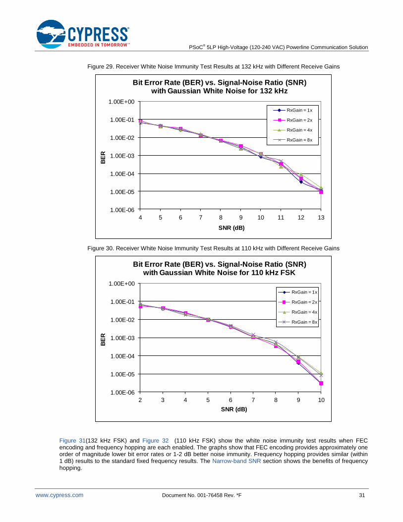
Figure 31(132 kHz FSK) and Figure 32 (110 kHz FSK) show the white noise immunity test results when FEC encoding and frequency hopping are each enabled. The graphs show that FEC encoding provides approximately one order of magnitude lower bit error rates or 1-2 dB better noise immunity. Frequency hopping provides similar (within 1 dB) results to the standard fixed frequency results. The Narrow-band SNR section shows the benefits of frequency hopping.
1.00E-06
1.00E-05
1.00E-04
1.00E-03
1.00E-02
1.00E-01
1.00E+00
4 5 6 7 8 9 10 11 12 13
BE
R
SNR (dB)
Bit Error Rate (BER) vs. Signal-Noise Ratio (SNR) with Gaussian White Noise for 132 kHz
RxGain = 1x
RxGain = 2x
RxGain = 4x
RxGain = 8x
1.00E-06
1.00E-05
1.00E-04
1.00E-03
1.00E-02
1.00E-01
1.00E+00
2 3 4 5 6 7 8 9 10
BE
R
SNR (dB)
Bit Error Rate (BER) vs. Signal-Noise Ratio (SNR) with Gaussian White Noise for 110 kHz FSK
RxGain = 1x
RxGain = 2x
RxGain = 4x
RxGain = 8x

PSoC® 5LP High-Voltage (120-240 VAC) Powerline Communication Solution
www.cypress.com Document No. 001-76458 Rev. *F 32
Figure 31. Receiver White Noise Immunity Test Results at 132 kHz with FEC and Frequency Hopping
Figure 32. Receiver White Noise Immunity Test Results at 110 kHz with FEC and Frequency Hopping
1.00E-06
1.00E-05
1.00E-04
1.00E-03
1.00E-02
1.00E-01
1.00E+00
2 3 4 5 6 7 8 9 10
BE
R
SNR (dB)
Bit Error Rate (BER) vs. Signal-Noise Ratio (SNR) with Gaussian White Noise for 132 kHz FSK
Standard
FEC
Enabled
Frequency
Hopping
1.00E-06
1.00E-05
1.00E-04
1.00E-03
1.00E-02
1.00E-01
1.00E+00
2 3 4 5 6 7 8 9 10
BE
R
SNR (dB)
Bit Error Rate (BER) vs. Signal-Noise Ratio (SNR) with Gaussian White Noise for 110 kHz FSK
Standard
FEC
Enabled
Frequency
Hopping

PSoC® 5LP High-Voltage (120-240 VAC) Powerline Communication Solution
www.cypress.com Document No. 001-76458 Rev. *F 33
6.4.2 Narrow-band SNR
For this test, the waveform generator is set to Sine mode. We vary the frequency and amplitude of the noise until the packet success rate is greater than 99 percent (BER less than 10
-4). The bit error rate (BER) calculation is the same
as for the receiver sensitivity test. To calculate the signal-noise ratio (SNR), subtract the noise level from the PLC signal. A lower SNR for a fixed success rate means that the receiver can tolerate more noise relative to the PLC signal. For example, a -20 dB SNR value means that the noise can be ten times larger than the PLC signal and the device will still be able to properly receive the PLC signal.
Figure 33 shows the results of the narrow-band SNR test. The SNR is less than -17 dB for frequencies that are at least 3 dB away from the PLC signal (that is, outside the range of 127 - 136 kHz). Therefore, outside of this narrow window (referred to as out-of-band SNR), the noise must be at least 5 times larger than the PLC signal in order to have a BER greater than 10
-4.
When the receive gain changes from 1x to 2x, the minimum out-of-band SNR increases by approximately 2 dB because the receiver amplifies the noise more and it saturates the PLC signal. When the receive gain is 4x, the minimum out-of-band SNR increases by as much as 6 dB. When the receive gain is 8x, the minimum out-of-band SNR increases by as much as 12 dB. Therefore, for most powerline environments, the receive gain should be 1x or 2x to minimize the sensitivity to noise.
Figure 33. Narrow-band Noise Immunity Test Results at 132 kHz
Figure 34 shows the results of the narrow-band SNR test at 110 kHz FSK. The SNR is less than -17 dB for frequencies that are at least 3 dB away from the PLC signal (that is, outside the range of 106 - 114 kHz). Therefore, outside of this narrow window (referred to as out-of-band SNR), the noise must be at least 5 times larger than the PLC signal in order to have a BER greater than 10
-4.
-50-45-40-35-30-25-20-15-10
-505
10
60 80 100 120 140 160 180 200
SNR
(d
B)
Noise Frequency (kHz)
Minimum SNR vs Noise Frequency for BER > 10E-4 at 132 kHz FSK
RxGain = 1x
RxGain = 2x
RxGain = 4x
RxGain = 8x

PSoC® 5LP High-Voltage (120-240 VAC) Powerline Communication Solution
www.cypress.com Document No. 001-76458 Rev. *F 34
Figure 34. Narrow-band Noise Immunity Test Results at 110 kHz
When FEC encoding is enabled, the noise immunity improves by 0 – 2 dB. Figure 35 shows the results of the narrow-band SNR test when frequency hopping is enabled. In this case, the SNR is less than -30 dB across all noise frequencies because the system automatically selects the FSK center frequency that is not near the noise frequency.
Figure 35. Narrow-band Noise Immunity Test Results with Frequency Hopping
-50-45-40-35-30-25-20-15-10
-505
10
60 80 100 120 140 160 180 200
SNR
(d
B)
Noise Frequency (kHz)
Minimum SNR vs Noise Frequency for BER > 10E-4 at 110 kHz FSK
-50-45-40-35-30-25-20-15-10
-505
10
60 80 100 120 140 160 180 200
SNR
(d
B)
Noise Frequency (kHz)
Minimum SNR vs Noise Frequency for BER > 10E-4 with Frequency Hopping
Fixed 132k
Fixed 110k
Frequency Hopping
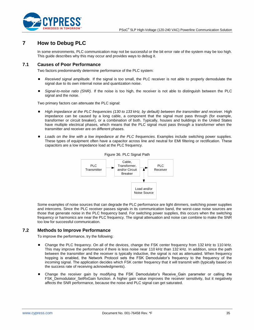
PSoC® 5LP High-Voltage (120-240 VAC) Powerline Communication Solution
www.cypress.com Document No. 001-76458 Rev. *F 35
7 How to Debug PLC
In some environments, PLC communication may not be successful or the bit error rate of the system may be too high. This guide describes why this may occur and provides ways to debug it.
7.1 Causes of Poor Performance
Two factors predominantly determine performance of the PLC system:
Received signal amplitude. If the signal is too small, the PLC receiver is not able to properly demodulate the signal due to its own internal noise and quantization noise.
Signal-to-noise ratio (SNR). If the noise is too high, the receiver is not able to distinguish between the PLC signal and the noise.
Two primary factors can attenuate the PLC signal:
High impedance at the PLC frequencies (130 to 133 kHz, by default) between the transmitter and receiver. High
impedance can be caused by a long cable, a component that the signal must pass through (for example, transformer or circuit breaker), or a combination of both. Typically, houses and buildings in the United States have multiple electrical phases, which means that the PLC signal must pass through a transformer when the transmitter and receiver are on different phases.
Loads on the line with a low impedance at the PLC frequencies. Examples include switching power supplies.
These types of equipment often have a capacitor across line and neutral for EMI filtering or rectification. These capacitors are a low impedance load at the PLC frequency.
Figure 36. PLC Signal Path
PLC
Transmitter
Cable,
Transformer,
and/or Circuit
Breaker
PLC
Receiver
Load and/or
Noise Source
Some examples of noise sources that can degrade the PLC performance are light dimmers, switching power supplies and intercoms. Since the PLC receiver passes signals in its communication band, the worst-case noise sources are those that generate noise in the PLC frequency band. For switching power supplies, this occurs when the switching frequency or harmonics are near the PLC frequency. The signal attenuation and noise can combine to make the SNR too low for successful communication.
7.2 Methods to Improve Performance
To improve the performance, try the following:
Change the PLC frequency. On all of the devices, change the FSK center frequency from 132 kHz to 110 kHz. This may improve the performance if there is less noise near 110 kHz than 132 kHz. In addition, since the path between the transmitter and the receiver is typically inductive, the signal is not as attenuated. When frequency hopping is enabled, the Network Protocol sets the FSK Demodulator’s frequency to the frequency of the incoming signal. The application decides which FSK center frequency that it will transmit with (typically based on the success rate of receiving acknowledgments).
Change the receiver gain by modifying the FSK Demodulator’s Receive_Gain parameter or calling the FSK_Demodulator_SetRxGain function. A higher gain value improves the receiver sensitivity, but it negatively affects the SNR performance, because the noise and PLC signal can get saturated.

PSoC® 5LP High-Voltage (120-240 VAC) Powerline Communication Solution
www.cypress.com Document No. 001-76458 Rev. *F 36
Increase the transmit amplitude by reducing the FSK Modulator’s Tx_Amplitude_Divider parameter or calling the FSK_Modulator_SetTxAmplitude function. This will drive a larger signal on to the powerline at the expense of higher power consumption.
Enable FEC encoding by setting the Network Protocol’s FEC_Encoding parameter or calling the Network_Protocol_EnableFec function. The Network Protocol encodes each 4-bit nibble of the packet into an 8-bit byte. If there is a single bit error in any of the bytes that are received on the other end of the line, the receiver’s Network Protocol will detect and correct the erroneous bit. Therefore, it improves the communication success rate at the expense of half the throughput of the original data.
Move the boards to be on the same electrical phase. This reduces the attenuation of the signal.
Turn off, disconnect, or change the socket of any potential noise sources or heavy loads. To measure the effect of removing a load, measure the noise floor and the maximum FSK level while a PLC device is transmitting. If the noise floor decreases or the maximum FSK level increases when the load is removed, it is an indication that the load has a negative effect on the PLC performance. The Network_Protocol_GetNoiseFloor and Network_Protocol_GetMaxFskLevel functions return the noise floor and maximum FSK level, respectively.
For more information on how to debug the PLC link, including techniques to identify and jump across powerline phases, block heavy loads and noise sources, and characterize the noise on the line, please read the application note AN58825 - PLC - Powerline Communication Debugging Tools.
8 Code Example Evaluation
This section provides a step-by-step description of how to evaluate the attached code example using boards manufactured according to the attached design files. A guide for this board is in Appendix B: PSoC 5LP PLC Hardware User’s Guide.
Figure 37 shows the PSoC Creator schematics of the code example. There are six functional blocks:
Demo User Interface: Contains an ADC for reading an analog voltage, an LCD to display the status of the demo, and digital input pins for a push-button and 8-port DIP switch.
External Host Interface (Optional): Contains three optional communication interfaces (I2C, RS232, and SPI) to configure the PLC system and transfer data
FSK Demodulator, Network Protocol, FSK Modulator: Contains the three PLC components along with the recommended external circuitry schematics.
Coupling Circuit: Shows one of the recommended circuits to couple the FSK signal to the powerline.
There are two options to evaluate the code example:
Standalone Demo: Evaluate the code example without a PC. The press of a push-button makes the system transmit packets from one board to another over the powerline. An ADC reads an analog voltage, the PLC protocol puts the voltage in a packet, and the modem transmits the packet. An LCD displays the communication statistics and the analog voltage received over the powerline.
External Host Interface: Evaluate the code example with the Cypress PLC Control Panel GUI on a PC. This option provides more configurability of the modem and network protocol.
CAUTION This board operates on high voltage 110 to 240 VAC lines. Use extreme caution when working with high voltage powerlines. Cover the high voltage section of the board with a protective casing to reduce the risk of shock. If there is no protective case, do not touch the board while it is plugged in.
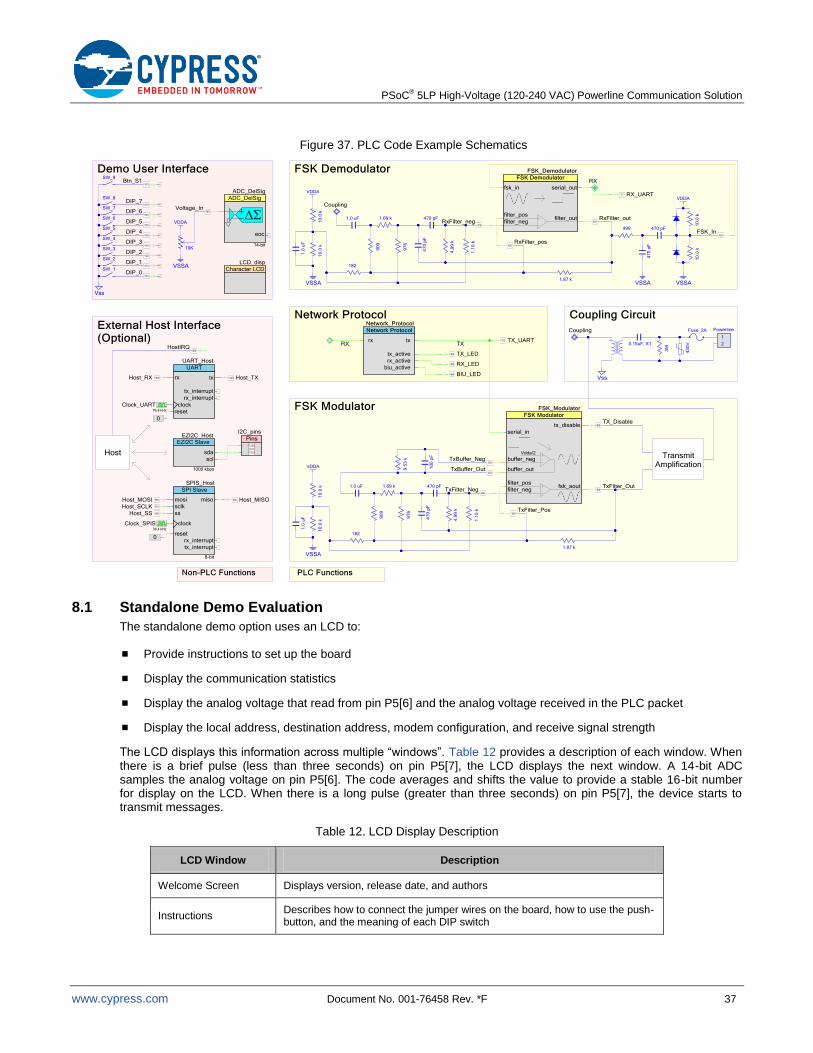
PSoC® 5LP High-Voltage (120-240 VAC) Powerline Communication Solution
www.cypress.com Document No. 001-76458 Rev. *F 37
Figure 37. PLC Code Example Schematics
8.1 Standalone Demo Evaluation
The standalone demo option uses an LCD to:
Provide instructions to set up the board
Display the communication statistics
Display the analog voltage that read from pin P5[6] and the analog voltage received in the PLC packet
Display the local address, destination address, modem configuration, and receive signal strength
The LCD displays this information across multiple “windows”. Table 12 provides a description of each window. When there is a brief pulse (less than three seconds) on pin P5[7], the LCD displays the next window. A 14-bit ADC samples the analog voltage on pin P5[6]. The code averages and shifts the value to provide a stable 16-bit number for display on the LCD. When there is a long pulse (greater than three seconds) on pin P5[7], the device starts to transmit messages.
Table 12. LCD Display Description
LCD Window Description
Welcome Screen Displays version, release date, and authors
Instructions Describes how to connect the jumper wires on the board, how to use the push-button, and the meaning of each DIP switch

PSoC® 5LP High-Voltage (120-240 VAC) Powerline Communication Solution
www.cypress.com Document No. 001-76458 Rev. *F 38
LCD Window Description
Statistics Displays the number of transmitted packets "T=", the number of received acknowledgments "A=", the number of received packets "R=", and the value of the received data payload "D="
Receive Signal Strength (in dB)
Displays the noise floor "NF=" and the maximum signal level "M=" for each FSK center frequency. Displays an '*' beside the active frequency
Config Displays the source address "SA=", the destination address "DA=", if FEC Encoding is enabled "FEC=", the active FSK center frequency "F=" and the receive gain "G="
TX Info Displays the number of transmitted packets "T=", the number of received acknowledgments "A=", and the recent success rate "S="
POT Values Displays the value of the on-board potentiometer "P=" and the value of the received data payload "D=", which is the remote device's potentiometer value
Scan Mode Displays each of the above fields individually with a more descriptive name
Pins P6[7:0] provide control over the PLC addressing, FEC Encoding, receiver gain, FSK center frequency, and frequency hopping, as shown in Table 13. The logic is inverted to support the DIP switches on the test board.
Table 13. Port 6 Pin Mapping
Pins Address
P6[1:0] Local Address
P6[3:2] Destination Address
P6[4] FEC Encoding (1=Disabled, 0=Enabled)
P6[5] Receiver Gain (1=0 dB, 0=6 dB)
P6[8:7] [1, 1] = 132 kHz Center Frequency
[0, 1] = 110 kHz Center Frequency
[1, 0] = Frequency Hopping
[0, 0] = Test Mode
8.1.1 Code Example Fi le Structure
The code for this application example is in multiple files for better readability and portability. These files are not necessary for PLC communication; they are only for this application example. The application example files are:
Analog.c Gathers and filters the streaming data from the ADC that samples pin P5[6]
Button.c Handles debounce, button press detection, and press/release detection
LCD.c Contains LCD helper functions
PLC_demo.c Processes the received PLC packets, transmits the analog voltage when there is the button event,
collects the communication statistics, and selects the best FSK center frequency (when frequency hopping is enabled)
State.c Manages the user interface by processing the button events and DIP switch settings, and updating the LCD

PSoC® 5LP High-Voltage (120-240 VAC) Powerline Communication Solution
www.cypress.com Document No. 001-76458 Rev. *F 39
8.1.2 Components Needed
The following components are required to evaluate the board with the standalone option. Example components shown in parenthesis.
One AC power cable per board. The cable must have an IEC 320-C7 connector (Qualtek 223020-01 6 ft AC
Cable).
Two 0.1-inch spaced jumper shunts per board (Kobiconn 151-8030-E).
One 16x2 LCD Module per board (Lumex LCM-S01602DTR/A). In order to connect this module to the board,
solder a 14-pin male header onto the module first (TE Connectivity AMP Connectors 87227-7).
One 2-inch (or longer) jumper wire per board.
One CY8CKIT-002 MiniProg3 programmer with USB cable.
A protective plastic case that covers the high voltage area (GDA Creative CLC551-NR).
8.1.3 Evaluation Steps
Follow these steps to evaluate the standalone code example:
1. On each board, place a jumper shunt across PWR and 10 V on the TXAMP header. Place a second jumper across PWR and 5 V on the FILTER header.
These set the power rails for the transmit amplification and filters. The FILTER header must only connect to the 5 V rail. If it connects to the 10 V rail, it may damage the PSoC 5LP device.
Figure 38. Jumper Shunts for Power Rails
2. On each board, connect a wire from P57 to S1 and a wire from P56 to VR. S1 is a button and VR is a potentiometer.
Figure 39. Connections from P57 to S1 and P56 to VR
3. Connect the LCD module to the LCD1 connector on each board. The LCD should stick outwards from the board.
4. Connect power cables from the mains to each board. The blue power LED should light up.
5. Open the attached code example in PSoC Creator.

PSoC® 5LP High-Voltage (120-240 VAC) Powerline Communication Solution
www.cypress.com Document No. 001-76458 Rev. *F 40
6. In bridgeLayer.h, set the host interface to local:
#define HOST_INTERFACE HOST_LOCAL
7. Connect the USB cable from the PC to the MiniProg3 programmer and connect the 10-pin ribbon cable from the MiniProg3 to the programming connector on one of the PLC boards.
Figure 40. MiniProg3 Programmer Connection
8. From PSoC Creator, select Debug > Program. If the Select Debug Target window appears, select the MiniProg3 item, and then click Connect. Click OK.
The project builds and then programs the device. The Output window displays the message “Device 'PSoC 5LP CY8C5868AXI-LP035*' was successfully programmed”.
9. Connect the MiniProg3 to the other board and repeat step 8.
The LCD on each board displays an introduction message and instructions. If nothing appears on the LCD, turn the potentiometer R46 to increase the contrast.
Figure 41. LCD Display of Programmed Board
10. The 8-port DIP switch sets some basic parameters of the PLC demo board. Table 14 shows the bit mapping.
In most cases, the DIP switches can be left in the OFF position. Instructions also appear on the LCD in the “Config” window.
LCD Contrast Control

PSoC® 5LP High-Voltage (120-240 VAC) Powerline Communication Solution
www.cypress.com Document No. 001-76458 Rev. *F 41
Table 14. DIP Switch Port Mapping
Figure 42. DIP Switch
DIP Port Address
[2:1] Local Address
[4:3] Destination Address
[5] FEC Encoding (ON=Enabled, OFF=Disabled)
[6] Receiver Gain (OFF=0 dB, ON=6 dB)
[8:7] [OFF, OFF] = 132 kHz Center Frequency
[ON, OFF] = 110 kHz Center Frequency
[OFF, ON] = Frequency Hopping
[ON, ON] = Test Mode
11. Press button S1 to show the “Statistics” window on the LCD.
12. On one of the boards, press and hold button S1 for approximately 3 seconds.
The device starts to transmit messages, as indicated by the flashing green TX LED. In addition, in the “Statistics” window on the LCD, a message appears to indicate the transmission count (e.g. T=3127) and the acknowledgement count (for example, A=2754). If the amber BIU (Band-In-Use) LED turns on, then there is another PLC signal or excessive noise on the powerline. If it is noise, the device automatically attempts to adapt the threshold to be higher than the noise.
If the communications link is working, the destination board will receive messages. In the “Statistics” window on the LCD, a message appears to indicate the receive count (such as R=2944) and the received data (such as D=29912). The red RX LED flashes for each byte received.
If the link is not working, change the FSK frequency by changing DIP switches 7 and 8 for all of the boards. Also, try enabling FEC encoding by turning on DIP switch 5 or change the receiver gain by changing DIP switches 6. Refer to the How to Debug PLC section for more information and other debugging techniques.
13. To stop transmitting messages, press and hold button S1 for approximately 3 seconds. To reset the statistics, press the Reset button, which is near the programming header and LCD header.
8.2 External Host Interface Evaluation
8.2.1 Components Needed
The following components are required to evaluate the board with the PLC Control Panel GUI option. Example components shown in parenthesis.
One PC that runs the Cypress PLC Control Panel GUI.
One AC power cable per board. The cable should have an IEC 320-C7 connector (Qualtek 223020-01 6 ft AC
Cable).
Two 0.1-inch spaced jumper shunts per board (Kobiconn 151-8030-E).
One CY8CKIT-002 MiniProg3 programmer with USB cable.
At least one CY3240 USB-I2C Bridge board with USB cable. A second bridge board will allow two PLC boards to be configured and monitored at the same time.
It is recommended to have a protective plastic case that covers the high voltage area of each board (GDA Creative CLC551-NR).
8.2.2 Evaluation Steps
Follow these steps to evaluate the code example with the GUI:

PSoC® 5LP High-Voltage (120-240 VAC) Powerline Communication Solution
www.cypress.com Document No. 001-76458 Rev. *F 42
1. On each board, place a jumper shunt across PWR and 10 V on the TXAMP header. Place a second jumper across PWR and 5 V on the FILTER header.
These set the power rails for the transmit amplification and filters. The FILTER header must only connect to the 5 V rail. If it connects to the 10 V rail, it may damage the PSoC 5LP device.
Figure 43. Jumper Shunts for Power Rails
2. Connect power cables from the mains to each board.
The blue power LED lights up.
3. Open the attached code example in PSoC Creator.
4. In bridgelayer.h, set the host interface to I2C:
#define HOST_INTERFACE HOST_I2C
5. Connect the USB cable from the PC to the MiniProg3 programmer and connect the 10-pin ribbon cable from the MiniProg3 to the programming connector on one of the demonstration boards.
Figure 44. MiniProg3 Programmer Connection
6. From PSoC Creator, select Debug > Program. If the Select Debug Target window appears, select the MiniProg3 item and then click Connect. Click OK.
The project builds and programs the device.
7. Connect the MiniProg3 to the other board and repeat step 6.

PSoC® 5LP High-Voltage (120-240 VAC) Powerline Communication Solution
www.cypress.com Document No. 001-76458 Rev. *F 43
8. Connect a USB cable from the PC to the CY3240 USB-I2C bridge board. Connect the CY3240 board to the PLC board’s 5-pin I
2C connector.
Figure 45. CY3240 USB-I2C Bridge Connection
9. Open the PLC Control Panel GUI. Select Help > Users Guide. Follow the steps in section 1.3 of the user’s guide
to complete the evaluation. Disregard the item that says to remove all jumpers; keep the two jumper shunts on the TXAMP and FILTER headers.
9 Summary
This application note provides a complete, flexible, and easy-to-use solution that implements powerline communication (PLC) with the PSoC 5LP family of devices. Along with the attached code example and board design files, an engineer can quickly develop a robust PLC design that can be easily integrated into their system.
About the Author Name: Jeffrey Hushley
Title: Applications Engineer Senior Staff
Background: Powerline Communications, high-speed digital design, lighting protocols

PSoC® 5LP High-Voltage (120-240 VAC) Powerline Communication Solution
www.cypress.com Document No. 001-76458 Rev. *F 44
A Appendix A: PLC Configuration Array Configuration settings for the network protocol and modem are in the PLC_Config array (Table 15).
Table 15. PLC Configuration (PLC_Config) Array
Register Bit Offset
Offset Register Name 7 6 5 4 3 2 1 0
0 (0x00) IRQ_ENABLE IRQ_CLEAR IRQ_POLARITY IRQ_TX_BIU_
TIMEOUT IRQ_TX_NO_
ACK IRQ_TX_NO_ RESPONSE
IRQ_RX_PACKET_ DROPPED
IRQ_RX_DATA_ AVAILABLE
IRQ_TX_ COMPLETE
1 (0x01) LOGICAL_ADDRESS_LSB 8 - bit Logical Address / LSB for extended 16-bit address
2 (0x02) LOGICAL_ADDRESS_MSB MSB for 16-bit Extended Address
3 (0x03) GROUP_8BIT 8-bit Group Address
4 (0x04) GROUP_MULTI One Hot Encoded (e.g. if byte = 0b00010001, then member of groups #5 and #1)
5 (0x05) PLC_MODE TX_ENABLE RX_ENABLE LOCK_CONFIG BIU_DISABLE RX_
OVERWRITE
EXTENDED_ ADDRESSING_
MODE
IGNORE_ DESTINATION_
ADDRESS IGNORE_CRC
6 (0x06) TX_MESSAGE_LENGTH TX_SEND_ MESSAGE
Reserved TX_LENGTH_MASK
7 (0x07) TX_CONFIG TX_SA_TYPE_
MASK TX_DA_TYPE_MASK TX_ACK_MODE TX_RETRIES
8 (0x08) TX_DESTINATION_ADDRESS Remote Node Destination Address (8 bytes)
16 (0x10) TX_COMMAND_ID TX Command ID
17 (0x11) TX_DATA TX Data (31 bytes)
48 (0x30) BIU_THRESHOLD_CONFIG Reserved BIU_AUTOSET Reserved BIU_THRESHOLD_MASK
49 (0x31) MODEM_CONFIG Reserved MODEM_TX_DELAY_MASK Reserved MODEM_BPS_MASK
50 (0x32) TX_AMPLITUDE Reserved TX_AMPLITUDE_MASK
51 (0x33) RX_GAIN Reserved RX_GAIN_MASK
52 (0x34) PROTOCOL_TIMING_CONFIG BIU_INTERVAL_MIN_MASK BIU_INTERVAL_SPAN_MASK BIU_INSTANT_
TIMEOUT Reserved ACK_TIMEOUT_MASK
53 (0x35) FSK_CONFIG Reserved FSK_FREQUENCY_MASK
54 (0x36) PROTOCOL_ENCODING_CONFIG Reserved
55-63 (0x37-0x3F)
Reserved Reserved FEC_ENABLE
64 (0x40) RX_MESSAGE_INFO RX_NEW_ MESSAGE
RX_DA_TYPE_ MASK
RX_SA_TYPE_ MASK
RX_LENGTH_MASK
65 (0x41) RX_SOURCE_ADDRESS Remote Node Source Address(8 Bytes)
73 (0x49) RX_COMMANDID RX Command ID
74 (0x4a) RX_DATA RX Data (31 bytes)
105 (0x69) PLC_STATUS STATUS_VALUE_
CHANGE Reserved
STATUS_TX_ BIU_TIMEOUT
STATUS_TX_ NO_ACK
STATUS_TX_ NO_RESPONSE
STATUS_RX_ PACKET_ DROPPED
STATUS_RX_ DATA_
AVAILABLE
STATUS_TX_ COMPLETE
106 (0x6A) PHYSICAL_ADDRESS Physical Address (8 bytes), "0x6A -> MSB"
114 (0x72) FW_VERSION Version Number

PSoC® 5LP High-Voltage (120-240 VAC) Powerline Communication Solution
www.cypress.com Document No. 001-76458 Rev. *F 45
Table 16 provides a description of each of the parameters in the PLC_Config array. The Access column describes
whether the application should write (“W”) to that parameter or read (“R”) that parameter. When an application writes to a parameter, the protocol reads the parameter and processes it (e.g. TX_DATA). When an application should read a parameter, the protocol writes to it (e.g. RX_DATA). When a parameter is read/write (“R/W”), the protocol typically writes one value and the application writes the other value. For example, when there is a new message received, the protocol sets the parameter RX_NEW_MESSAGE to ‘1’. When the application has read all of the data from the received message, it must set the parameter RX_NEW_MESSAGE to ‘0’. This tells the protocol to clear its receive buffer and prepare to receive a new message. The application can modify parameters that have read access. For example, the application clears the PLC_STATUS byte after it has processed the event. The difference is that the protocol does not read from this byte and perform an action. It only writes to this byte when there is a new event. However, when an external host runs the application via I
2C, it must not write to the parameters that have read
access because the host could write to the byte at the same time that the protocol writes to the byte. This could cause the host to overwrite a status update and miss an event. Instead, the host writes a ‘0’ to the IRQ_CLEAR parameter, which clears only the transmit status parameters in the PLC_STATUS byte. To clear the receive status parameters, the host writes a ‘0’ to the RX_NEW_MESSAGE parameter.
Table 16. PLC_Config Parameter Description
Field Name Access Size Description
IRQ_ENABLE (Offset 0x00)
IRQ_CLEAR R/W 1 0 - When the host writes a '0' to this field, the protocol de-asserts the HostIRQ pin and clears the PLC_Status register (except for STATUS_RX_PACKET_DROPPED and STATUS_RX_DATA_AVAILABLE).
1 - When there is a new event, the protocol sets this bit to '1'.
IRQ_POLARITY W 1 0 - The HostIRQ pin is active low.
1 - The HostIRQ pin is active high.
IRQ_TX_BIU_TIMEOUT W 1 0 - A BIU timeout event does not affect the HostIRQ pin.
1 – The protocol asserts the HostIRQ pin when a BIU timeout event occurs.
IRQ_TX_NO_ACK W 1 0 - An acknowledgment timeout event does not affect the HostIRQ pin.
1 - The protocol asserts the HostIRQ pin when it expects an acknowledgment but does not receive one within the time window defined by the ACK_TIMEOUT_MASK parameter.
IRQ_TX_NO_RESPONSE W 1 0 - A response timeout event does not affect the HostIRQ pin.
1 - The protocol asserts the HostIRQ pin when it transmits a CMD_REQUEST_DATA message, but does not receive a CMD_RESPONSE_DATA message within 1.5 seconds.
IRQ_RX_PACKET_DROPPED W 1 0 - A dropped packet event does not affect the HostIRQ pin.
1 - The protocol asserts the HostIRQ pin when it has an unread message in the buffer and a second message is received. That new message is dropped.
IRQ_RX_DATA_AVAILABLE W 1 0 - A new received packet event does not affect the HostIRQ pin.
1 -The protocol asserts the HostIRQ pin when a new packet is received.
IRQ_TX_COMPLETE W 1 0 - A completed transmission event does not affect the HostIRQ pin.
1 (when TX_ACK_MODE = 0) - The protocol asserts the HostIRQ pin when it transmits the complete packet. 1 (when TX_ACK_MODE = 1) - The protocol asserts the HostIRQ pin when it transmits the complete packet and it receives an acknowledgment.
PLC_MODE (0x05)
TX_ENABLE W 1 0 - The transmitter can transmit messages.
1 - The transmitter cannot receive messages.
RX_ENABLE W 1 0 - The receiver can receive messages.
1 - The receiver cannot receive messages.
LOCK_CONFIG W 1 0 – The protocol allows the configuration commands (TX_COMMAND_ID = 0x01 - 0x0F) to change the configuration (TX Enable, Ext Address, Disable BIU, Threshold Value, Logical Address, Group Membership)
1 - The protocol prevents the configuration commands from changing the configuration.
BIU_DISABLE W 1 0 - Enables band-in-use detection.
1 - Disables band-in-use detection.

PSoC® 5LP High-Voltage (120-240 VAC) Powerline Communication Solution
www.cypress.com Document No. 001-76458 Rev. *F 46
Table 16. PLC_Config Parameter Description
Field Name Access Size Description
RX_OVERWRITE W 1 0 - If the receive buffer (RX_DATA) has an unread message, the protocol drops any new messages.
1 - If the receive buffer (RX_DATA) has an unread message, the protocol overwrites the existing message with the new message.
EXTENDED_ADDRESSING_MODE W 1 0 - 8-bit Logical Addressing mode
1 - 16-bit Extended Logical Addressing mode
Note This mode should be the same in all the devices in the network
IGNORE_DESTINATION_ADDRESS W 1 0 - The protocol drops the received packet if the destination address does not match the local address.
1- The protocol stores the received packet even if the destination address does not match the local address.
IGNORE_CRC W 1 0 - The protocol drops the received message if the 8-bit CRC fails.
1- The protocol stores the received message even if the 8-bit CRC fails.
TX_MESSAGE_LENGTH (0x06)
TX_SEND_MESSAGE R/W 1 0 - Transmitter is idle. The protocol automatically clears this bit when:
- (TX_ACK_MODE = 0) It transmits the complete packet.
-(TX_ACK_MODE = 1) It transmits the complete packet and it receives the acknowledgment or the acknowledgment timeout occurs.
1 - The protocol transmits a message once the powerline is free.
Note The application should set the TX_CONFIG, TX_DESTINATION_ADDRESS,
TX_COMMAND_ID and TX_DATA registers before it sets this bit to ‘1’.
TX_LENGTH_MASK W 5 The length of the data payload in TX_DATA. The payload length can be 0 to 31.
TX_CONFIG (0x07)
TX_SA_TYPE_MASK W 1 0 - The source address in the transmitted packet is this device's logical address (8-bit or 16-bit, depending on EXTENDED_ADDRESSING_MODE).
1 - The source address in the transmitted packet is this device's 64-bit physical address.
TX_DA_TYPE_MASK W 2 00 - The destination address in the transmitted packet is a logical address (8-bit or 16-bit, depending on EXTENDED_ADDRESSING_MODE).
01 - The destination address in the transmitted packet is an 8-bit group address.
10 - The destination address in the transmitted packet is a 64-bit physical address.
11 - Invalid
TX_ACK_MODE W 1 0 - After the protocol transmits a packet, it does not expect an acknowledgment.
1 - After the protocol transmits a packet, it expects the destination to transmit back an acknowledgment.
TX_RETRIES W 4 If TX_ACK_MODE = 0, the protocol transmits the packet 1 + TX_RETRIES times.
If TX_ACK_MODE = 1, the protocol re-transmits the packet up to TX_RETRIES times for each time that the ACK_TIMEOUT_MASK time expires.
TX_DESTINATION_ADDRESS (0x08 - 0x0F)
8-bit Logical Address W 8 Byte Offset 0x08
16-bit Logical Address W 16 Byte Offset 0x08 – LSB
Byte Offset 0x09 – MSB
64-bit Physical Address W 64 Byte Offset 0x08 – MSB
Byte Offset 0x0F – LSB
BIU_THRESHOLD_CONFIG (0x30)
BIU_AUTOSET R/W 1 0 - Auto Set Threshold is disabled. When the auto set threshold function completes, the protocol clears this parameter to ‘0’.
1 - When the protocol is idle, the protocol sets the BIU threshold (BIU_THRESHOLD_MASK) to the lowest value that does not cause a BIU detection.
BIU_THRESHOLD_MASK W 4 Band-In-Use (BIU) detection threshold. When a signal is higher than the following level for at
PSoC® 5LP High-Voltage (120-240 VAC) Powerline Communication Solution
www.cypress.com Document No. 001-76458 Rev. *F 47
Table 16. PLC_Config Parameter Description
Field Name Access Size Description
least 4 ms, a BIU detection event occurs and the timer restarts.
0000 - 43 dBµVrms
0001 - 50 dBµVrms
0010 - 57 dBµVrms
0011 - 63 dBµVrms
0100 - 69 dBµVrms
0101 - 75 dBµVrms
0110 - 82 dBµVrms
0111 - 85 dBµVrms
1000 - 88 dBµVrms
1001 - 91 dBµVrms
1010 - 94 dBµVrms
1011 - 97 dBµVrms
1100 - 100 dBµVrms
1101 - 103 dBµVrms
1110 - 106 dBµVrms
1111 - 109 dBµVrms
MODEM_CONFIG (0x31)
MODEM_TX_DELAY_MASK W 1 Before the transmitter sends the packet, it drives the logic '1' FSK frequency for the following amount of time, so that the receiver’s UART can clear its buffer and be ready for the packet.
Note This value is automatically set when the application changes the baud rate (2400 bps =>
7 ms, 1800 bps => 13 ms, 1200 bps => 19 ms, 600 bps => 25 ms). A lower value is not recommended.
00 - 7 ms
01 - 13 ms
10 – 19 ms
11 – 25 ms
MODEM_BPS_MASK W 2 Baud Rate:
00 - 600 bps
01 - 1200 bps
10 - 1800 bps
11 – 2400 bps (default)
TX_AMPLITUDE (0x32)
TX_AMPLITUDE_MASK W 4 Transmit Amplitude:
0000 - (-46 dB)
0001 - (-42 dB)
0010 - (-40 dB)
0011 - (-36 dB)
0100 - (-34 dB)
0101 - (-30 dB)
0110 - (-28 dB)
0111 - (-24 dB)
1000 - (-22 dB)
1001 - (-18 dB)
1010 - (-16 dB)
1011 - (-12 dB)
1100 - (-10 dB)
1101 - (-6 dB) (default)
1110 - (-4 dB)
1111 - (0 dB)

PSoC® 5LP High-Voltage (120-240 VAC) Powerline Communication Solution
www.cypress.com Document No. 001-76458 Rev. *F 48
Table 16. PLC_Config Parameter Description
Field Name Access Size Description
RX_GAIN (0x33)
RX_GAIN_MASK W 4 Receive Amplifier Gain:
0000 - 1x
0001 - 2x
0010 - 4x
0011 - 8x
0100 - 16x
0101 - 24x
0110 - 32x
0111 - 48x
1000 - 50x
PROTOCOL_TIMING_CONFIG (0x34)
BIU_INTERVAL_MIN_MASK W 2 Minimum time of the random interval for BIU detection:
00 – 85 ms
01 – 50 ms
10 – 20 ms
11 – 10 ms
BIU_INTERVAL_SPAN_MASK W 2 Span from the minimum to the maximum time of the random interval for BIU detection:
00 – 30 ms
01 – 15 ms
10 – 1 ms
BIU_INSTANT_TIMEOUT W 1 The maximum amount of time to wait for the line to be free:
0 – 1.1 second timeout
1 – Timeout on first BIU detection
ACK_TIMEOUT_MASK W 2 The maximum amount of time to wait for an acknowledgment to be received. The "Auto +" settings mean that the protocol calculates the expected time that it takes for the acknowledgment to be transmitted back. This is based on the acknowledgment’s packet length and baud rate.
00 – 500 ms
01 – Auto + 100 ms
10 – Auto + 50 ms
11 – Auto + 20 ms
FSK_CONFIG (0x35)
FSK_FREQUENCY_MASK W 4 FSK Carrier Frequency:
1011 – Logic '0' = 111.1 kHz, Logic '1' = 109.1 kHz
1101 – Logic '0' = 133.3 kHz, Logic '1' = 130.4 kHz (default)
All other values – Reserved
PROTOCOL_ENCODING_CONFIG (0x36)
FEC_ENABLE W 1 0 – The protocol does not perform FEC encoding on the transmitted packets.
1 – The protocol performs FEC encoding on the transmitted packets.
RX_MESSAGE_INFO (0x40)
RX_NEW_MESSAGE R/W 1 0 - The protocol does not have an unread message in its buffer.
1 - The protocol has an unread message in its buffer.
Note The application must set this bit to ‘0’ after it reads the RX Message. This allows the
protocol to receive a new RX message. This also clears the STATUS_RX_PACKET_DROPPED and STATUS_RX_DATA_AVAILABLE flags.
RX_DA_TYPE_MASK R 1 0 - The remote transmitter sent this received packet directly to this device.
1 - The remote transmitter sent this received packet to a group.
RX_SA_TYPE_MASK R 1 0 - The source address in the received packet is the source's logical address (8-bit or 16-bit, depending on EXTENDED_ADDRESSING_MODE).

PSoC® 5LP High-Voltage (120-240 VAC) Powerline Communication Solution
www.cypress.com Document No. 001-76458 Rev. *F 49
Table 16. PLC_Config Parameter Description
Field Name Access Size Description
1 - The source address in the received packet is the source's 64-bit physical address.
RX_LENGTH_MASK R 5 The length of the data payload in RX_DATA from 0 to 31
RX_SOURCE_ADDRESS (0x41 - 0x48)
8-bit Logical Address R 8 Byte Offset 0x41
16-bit Logical Address R 16 Byte Offset 0x41 – LSB
Byte Offset 0x42 – MSB
64-bit Physical Address R 64 Byte Offset 0x41 – MSB
Byte Offset 0x48 – LSB
PLC_STATUS (0x69)
Note: When there is an external host, the protocol clears this register (except for STATUS_RX_DATA_AVAILABLE) when the application sets INT Clear to Logic 0. Otherwise, the application can clear any of these parameters with a direct memory write to this byte.
STATUS_VALUE_CHANGE R 1 0 - No new events have occurred.
1 - A new event has occurred.
STATUS_TX_BIU_TIMEOUT R 1 0 - No band-in-use timeout event has occurred.
1 - A band-in-use timeout event has occurred.
STATUS_TX_NO_ACK R 1 0 - No ACK timeout event has occurred.
1 - The protocol expected an acknowledgment (TX_ACK_MODE = 1), but it didn’t receive one within the time window defined by the ACK_TIMEOUT_MASK parameter.
STATUS_TX_NO_RESPONSE R 1 0 (When the protocol transmitted a CMD_REQUEST_DATA message and STATUS_TX_COMPLETE = 1) - The protocol received a CMD_RESPONSE_DATA message within 1.5 seconds.
0 (Otherwise) - The protocol did not expect a response.
1 - The protocol transmitted a CMD_REQUEST_DATA message, but it did not receive a CMD_RESPONSE_DATA message within 1.5 seconds.
STATUS_RX_PACKET_DROPPED R 1 0 - The protocol did not drop any received packets.
1 - The protocol dropped a receive packet, because there is an unread message in the receiver’s buffer and the RX_OVERWRITE parameter is ‘0’.
STATUS_RX_DATA_AVAILABLE R 1 0 - The protocol does not have an unread message in its buffer.
1 - The protocol has an unread message in its buffer.
STATUS_TX_COMPLETE R 1 0 - The protocol is not transmitting or has not completed transmitting the packet.
1 (TX_ACK_MODE = 0) - The protocol transmitted the complete packet.
1 (TX_ACK_MODE = 1) - The protocol transmitted the complete packet, and it received an acknowledgment.

PSoC® 5LP High-Voltage (120-240 VAC) Powerline Communication Solution
www.cypress.com Document No. 001-76458 Rev. *F 50
B Appendix B: PSoC 5LP PLC Hardware User’s Guide This section describes how to use the features of the PSoC 5LP PLC test board. The attached design files can be used to manufacture this board. .
CAUTION This board operates on high voltage 110 to 240 VAC lines. Use extreme caution when working with high voltage powerlines. Cover the high voltage section of the board with a protective casing to reduce the risk of shock. If there is no protective case, do not touch the board while it is plugged in.
Figure 46. PSoC 5LP PLC Test Board Annotated
Coupling Circuit
Power Supply
Breadboard
User Potentiometer
User Buttons
LCD Contrast Potentiometer
PLC Status LEDs
DIP Switches
LCD Card Connector
Reset Button
Programming Connector
24 MHz Crystal
RS232 Connector and Transceiver
TX Amplification
I2C Connector and Jumpers
TX Filter
RX Filter
PSoC 5
User LEDs

PSoC® 5LP High-Voltage (120-240 VAC) Powerline Communication Solution
www.cypress.com Document No. 001-76458 Rev. *F 51
B.1 Board Component Description
This section provides a description of the different components on the board and explains how to use them.
B.1.1 PLC Fi l ters, Ampli f icat ion , and Test Points
Figure 47 shows the PLC filters and amplification circuits. The transmit filter is in the top right quadrant, the receive filter is in the bottom right quadrant, and the transmit amplifier is on the left side. The test points (listed in order from the top of the figure to the bottom) are:
VSSA: A clean analog ground reference
TX: The output from the PSoC 5LP’s opamp I-V buffer. It is the input to the transmitter’s low-pass notch filter.
TXFILT: The output of the transmitter’s low-pass notch filter.
TXSHDN: The signal from the PSoC 5LP that controls the state of the transmit amplifier. When it is HIGH, the amplifier is placed in a high-impedance state.
RX: The output of the receiver’s filters. It connects directly to the receiver input of the PSoC 5LP.
FSK: The point that connects the transmitter and receiver with the coupling circuit.
RXFILT: With the existing board configuration, this test point is the same as the FSK test point.
Figure 47. PLC Filters, Amplification, and Test Points
B.1.2 PLC Indicator LEDs
There are three LEDs to indicate the status of the PLC system (Figure 48):
TX (Green LED): The device is transmitting a PLC signal on the powerline.
RX (Red LED): The device received a valid byte of data and stored it in the buffer. A valid byte of data means that the data matches the PLC packet structure. The protocol must receive the preamble before the RX LED turns on. If the destination address matches the local address, the RX LED stays on until the device receives the last byte or an invalid byte.
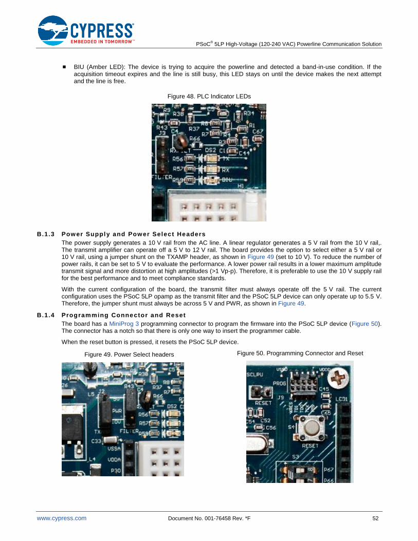
PSoC® 5LP High-Voltage (120-240 VAC) Powerline Communication Solution
www.cypress.com Document No. 001-76458 Rev. *F 52
BIU (Amber LED): The device is trying to acquire the powerline and detected a band-in-use condition. If the acquisition timeout expires and the line is still busy, this LED stays on until the device makes the next attempt and the line is free.
Figure 48. PLC Indicator LEDs
B.1.3 Power Supply and Power Select Headers
The power supply generates a 10 V rail from the AC line. A linear regulator generates a 5 V rail from the 10 V rail,. The transmit amplifier can operate off a 5 V to 12 V rail. The board provides the option to select either a 5 V rail or 10 V rail, using a jumper shunt on the TXAMP header, as shown in Figure 49 (set to 10 V). To reduce the number of power rails, it can be set to 5 V to evaluate the performance. A lower power rail results in a lower maximum amplitude transmit signal and more distortion at high amplitudes (>1 Vp-p). Therefore, it is preferable to use the 10 V supply rail for the best performance and to meet compliance standards.
With the current configuration of the board, the transmit filter must always operate off the 5 V rail. The current configuration uses the PSoC 5LP opamp as the transmit filter and the PSoC 5LP device can only operate up to 5.5 V. Therefore, the jumper shunt must always be across 5 V and PWR, as shown in Figure 49.
B.1.4 Programming Connector and Reset
The board has a MiniProg 3 programming connector to program the firmware into the PSoC 5LP device (Figure 50). The connector has a notch so that there is only one way to insert the programmer cable.
When the reset button is pressed, it resets the PSoC 5LP device.
Figure 49. Power Select headers
Figure 50. Programming Connector and Reset

PSoC® 5LP High-Voltage (120-240 VAC) Powerline Communication Solution
www.cypress.com Document No. 001-76458 Rev. *F 53
B.1.5 I2C Connector and Jumpers
The I2C connector connects a CY3240 USB-I2C Bridge board from a PC to the PLC board. The Cypress PLC Control
Panel GUI can configure the PLC board to transmit and receive messages. The Cypress PLC Control Panel GUI can be downloaded here.
The attached code example supports an I2C interface via pins P12[0] and P12[1] for SCL and SDA, respectively.
These pins are hardwired to the I2C connector. The EZI2Cs component transmits and receives the data.
The I2C connector can also connect to any other board via I
2C (up to 400 kbps). As shown in Figure 51, the 5-pin
connector is labeled as follows (from left to right):
V: 5 V power, which can be supplied to an external board (up to 20 mA). The PWR jumper must have a shunt across its pins.
G: Ground.
R: Reset. When the RESET jumper has a shunt across its pins, this pin will allow an external board to reset the PSoC 5LP device.
C: I2C SCL (Clock)
D: I2C SDA (Data)
There are four jumpers associated with the I2C connector (from left to right in Figure 51):
PWR: When the user places a jumper shunt on it, the 5 V rail connects to the V pin on the I2C connector. It can
supply up to 20 mA to an external board.
SCLPU: When the user places a jumper shunt on it, the I2C SCL line connects to a pull-up resistor, which is
required for I2C communication. If the external board already has a pull-up resistor (as with the CY3240 USB-I2C
bridge), then a shunt is not necessary.
SDAPU: When the user places a jumper shunt on it, the I2C SDA line connects to a pull-up resistor, which is
required for I2C communication. If the external board already has a pull-up resistor (as with the CY3240 USB-I2C
bridge), then a shunt is not necessary.
RESET: When the user places a jumper shunt on it, the R pin on the I2C connector connects directly to the
RESET pin on the PSoC 5LP device.
Figure 51. I2C Connector and Jumpers
B.1.6 RS232 Connector
This connector provides the ability to connect an external system to the PSoC 5LP device via an RS232 interface. The board has an RS232 transceiver for level translation and a standard DB-9 female connector, as shown in Figure 52.
The attached code example supports an RS232 interface via pins P12[7] and P12[6] for TX and RX, respectively. These pins are hardwired to the RS232 transceiver. The Host_UART component transmits and receives the data.

PSoC® 5LP High-Voltage (120-240 VAC) Powerline Communication Solution
www.cypress.com Document No. 001-76458 Rev. *F 54
Figure 52. RS232 Connector
B.1.7 Prototyping Area and GPIO Headers
The prototyping area includes a breadboard and headers to access most of the available GPIOs from the PSoC 5LP device, as shown in Figure 53. The GPIO pins are:
VSSA: A clean analog ground
VDDA: A clean analog 5 V power rail
VSSD: Digital ground
VDDD: Digital 5 V power rail
Pxy: Port pin P[x]y (for example P30 is P3[0]). Port 0 and Port 3 pins have the following additional capabilities:
P30, P31, P06, P07: Can be IDAC outputs
P00, P04, P05: Can be opamp pins
A description of the other pins is in the next section.
Figure 53. Breadboard and GPIO Headers
B.1.8 LEDs , Push-but tons, and Potentiometer
The board has LEDs, push buttons, and a potentiometer to evaluate the system with some user I/Os. As shown in Figure 54, there are four red LEDs (LED1 – LED4), two push buttons (S2, S1), and a potentiometer (R47). These can connect to the PSoC 5LP device with a jumper wire from the associated header pin to one of the GPIO pins (for example, from S1 to P57).

PSoC® 5LP High-Voltage (120-240 VAC) Powerline Communication Solution
www.cypress.com Document No. 001-76458 Rev. *F 55
The LEDs are active HIGH. When the push-button is pressed, it connects the signal to ground. When not pressed, the signal is left floating. Therefore, the PSoC 5LP pin that connects to this push-button has a resistive pull-up drive mode. The potentiometer provides an analog voltage from 0 to 5 V.
Figure 54. LEDs, Push-buttons, and Potentiometer
B.1.9 DIP Switch
The 8-port DIP switch provides a quick way to set a value (for example, a PLC address). When the DIP switch is in the ON position, it connects the signal to ground. When the DIP switch is in the OFF position, the signal is left floating. Therefore, the PSoC 5LP pin has a resistive pull-up drive mode. Also, the logic is inverted so that ON means logic ‘1’.
The DIP switch is hardwired to port 6 of the PSoC 5LP device. Figure 55 shows the mapping where DIP switch 1 connects to P60, and so on.
Figure 55. DIP Switch

PSoC® 5LP High-Voltage (120-240 VAC) Powerline Communication Solution
www.cypress.com Document No. 001-76458 Rev. *F 56
B.1.10 LCD Card Connector and Contrast Dia l
The LCD card connector allows a connection to an LCD module, so that the PSoC 5LP device can easily display information to the user (with the PSoC Creator LCD component). The LCD contrast dial is a potentiometer that sets the contrast level of the LCD module. Figure 56 shows the connector and contrast dial.
Figure 56. LCD Card Connector and Contrast Dial
The Lumex LCM-S01602DTR/A LCD Module is compatible with this LCD connector and the PSoC Creator LCD component. It can be purchased here. To connect this module to the board, solder a 14-pin male header to the module first. This can be purchased here. The LCD card is attached to the board, as shown in Figure 57.
Figure 57. LCD Card Attached

PSoC® 5LP High-Voltage (120-240 VAC) Powerline Communication Solution
www.cypress.com Document No. 001-76458 Rev. *F 57
Document History
Document Title: AN76458 - PSoC® 5LP High Voltage (120-240 VAC) Powerline Communication Solution
Document Number: 001-76458
Revision ECN Orig. of Change
Submission Date
Description of Change
** 3702581 FRE 08/08/2012 New Spec.
*A 3820054 FRE 11/27/2012 Updated Associated Part Family to “CY8C56xx/CY8C58xx “.
Updated Software Version to “PSoC Creator™ 2.1 SP1”.
Replaced PSoC 5 with PSoC 5LP in all instances across the document.
*B 3934223 FRE 02/21/2013 Modularized the PLC firmware into three components (FSK Modulator, FSK Demodulator, and Network Protocol) and moved the details of these components to their new component data sheets (located in the code example)
Added two features: frequency hopping and receive signal strength indicator (RSSI). Added support for these features into the demo of the code example
Added control of FEC Encoding in the code example
Updated the results in the Performance section for the new design
Added “High Voltage (120-240 VAC)” to the title
Updated Software Version to “PSoC Creator™ 2.2”.
*C 4107850 MKEA 08/27/2013 Project corrected to incorporate the modularized PLC firmware from revision *B.
*D 4540443 DRSW 10/30/2014 Updated out of date contact information and document references.
*E 4985961 BOO 12/11/2015 Updated project to PSoC Creator 3.3 and fixed issues that generated warnings
Removed reference to low voltage app note that was not produced
Removed 3rd party hyperlinks
Updated to single column format
*F 5700387 AESATMP9 04/26/2017 Updated logo and copyright.

PSoC® 5LP High-Voltage (120-240 VAC) Powerline Communication Solution
www.cypress.com Document No. 001-76458 Rev. *F 58
Worldwide Sales and Design Support
Cypress maintains a worldwide network of offices, solution centers, manufacturer’s representatives, and distributors. To find the office closest to you, visit us at Cypress Locations.
Products
ARM® Cortex
® Microcontrollers cypress.com/arm
Automotive cypress.com/automotive
Clocks & Buffers cypress.com/clocks
Interface cypress.com/interface
Internet of Things cypress.com/iot
Memory cypress.com/memory
Microcontrollers cypress.com/mcu
PSoC cypress.com/psoc
Power Management ICs cypress.com/pmic
Touch Sensing cypress.com/touch
USB Controllers cypress.com/usb
Wireless Connectivity cypress.com/wireless
PSoC® Solutions
PSoC 1 | PSoC 3 | PSoC 4 | PSoC 5LP | PSoC 6
Cypress Developer Community
Forums | WICED IOT Forums | Projects | Videos | Blogs | Training | Components
Technical Support
Cypress.com/support
All other trademarks or registered trademarks referenced herein are the property of their respective owners.
Cypress Semiconductor 198 Champion Court San Jose, CA 95134-1709
© Cypress Semiconductor Corporation, 2012-2017. This document is the property of Cypress Semiconductor Corporation and its subsidiaries, including Spansion LLC (“Cypress”). This document, including any software or firmware included or referenced in this document (“Software”), is owned by Cypress under the intellectual property laws and treaties of the United States and other countries worldwide. Cypress reserves all rights under such laws and treaties and does not, except as specifically stated in this paragraph, grant any license under its patents, copyrights, trademarks, or other intellectual property rights. If the Software is not accompanied by a license agreement and you do not otherwise have a written agreement with Cypress governing the use of the Software, then Cypress hereby grants you a personal, non-exclusive, nontransferable license (without the right to sublicense) (1) under its copyright rights in the Software (a) for Software provided in source code form, to modify and reproduce the Software solely for use with Cypress hardware products, only internally within your organization, and (b) to distribute the Software in binary code form externally to end users (either directly or indirectly through resellers and distributors), solely for use on Cypress hardware product units, and (2) under those claims of Cypress’s patents that are infringed by the Software (as provided by Cypress, unmodified) to make, use, distribute, and import the Software solely for use with Cypress hardware products. Any other use, reproduction, modification, translation, or compilation of the Software is prohibited.
TO THE EXTENT PERMITTED BY APPLICABLE LAW, CYPRESS MAKES NO WARRANTY OF ANY KIND, EXPRESS OR IMPLIED, WITH REGARD TO THIS DOCUMENT OR ANY SOFTWARE OR ACCOMPANYING HARDWARE, INCLUDING, BUT NOT LIMITED TO, THE IMPLIED WARRANTIES OF MERCHANTABILITY AND FITNESS FOR A PARTICULAR PURPOSE. To the extent permitted by applicable law, Cypress reserves the right to make changes to this document without further notice. Cypress does not assume any liability arising out of the application or use of any product or circuit described in this document. Any information provided in this document, including any sample design information or programming code, is provided only for reference purposes. It is the responsibility of the user of this document to properly design, program, and test the functionality and safety of any application made of this information and any resulting product. Cypress products are not designed, intended, or authorized for use as critical components in systems designed or intended for the operation of weapons, weapons systems, nuclear installations, life-support devices or systems, other medical devices or systems (including resuscitation equipment and surgical implants), pollution control or hazardous substances management, or other uses where the failure of the device or system could cause personal injury, death, or property damage (“Unintended Uses”). A critical component is any component of a device or system whose failure to perform can be reasonably expected to cause the failure of the device or system, or to affect its safety or effectiveness. Cypress is not liable, in whole or in part, and you shall and hereby do release Cypress from any claim, damage, or other liability arising from or related to all Unintended Uses of Cypress products. You shall indemnify and hold Cypress harmless from and against all claims, costs, damages, and other liabilities, including claims for personal injury or death, arising from or related to any Unintended Uses of Cypress products. Cypress, the Cypress logo, Spansion, the Spansion logo, and combinations thereof, WICED, PSoC, CapSense, EZ-USB, F-RAM, and Traveo are trademarks or registered trademarks of Cypress in the United States and other countries. For a more complete list of Cypress trademarks, visit cypress.com. Other names and brands may be claimed as property of their respective owners.
Related Documents