1 PS – ACC 8251 & 8253 www.pantechsolutions.net USART AND TIMER INTERFACE 8253&8251 PART NO: PS-ACC-8251 & 8253 FIRST EDITION USER MANUAL Pantech Solutions Pvt Ltd., No 41, Rajeswari Street, Santhosh Nagar, Kandhanchavadi (OMR), Chennai - 600 096, Tamilnadu, India. Ph: 044 - 64524445 /46/47 Fax: 044 – 4260 6350 www.pantechsolutions.net | Email: info@pantechsolutions.net Internet: Support : [email protected] Sales : [email protected] Hand Phone: Sales &Support : 91- 98409 74408 / 98402 95549

PS 8251&8253
Oct 24, 2015
microprocessor Lab
Welcome message from author
This document is posted to help you gain knowledge. Please leave a comment to let me know what you think about it! Share it to your friends and learn new things together.
Transcript

1
PS – ACC 8251 & 8253 www.pantechsolutions.net
USART AND TIMER INTERFACE
8253&8251
PART NO: PS-ACC-8251 & 8253
FIRST EDITION
USER MANUAL
Pantech Solutions Pvt Ltd., No 41, Rajeswari Street, Santhosh Nagar,
Kandhanchavadi (OMR), Chennai - 600 096, Tamilnadu, India.
Ph: 044 - 64524445 /46/47 Fax: 044 – 4260 6350
www.pantechsolutions.net | Email: [email protected]
Internet: Support : [email protected] Sales : [email protected]
Hand Phone: Sales &Support : 91- 98409 74408 / 98402 95549

2
PS – ACC 8251 & 8253 www.pantechsolutions.net
Introduction
Thank you for purchasing the Add-On Cards. You will find it useful in developing
your Controller/Processor based applications.
Packages
8251 & 8253 Add-on Card
Interface Cable
Reference Documents | Example Programs
Technical or Customer Support
E-mail questions to
Send questions by mail to
Pantech Solutions Pvt Ltd.,
#41, Santhosh Nagar,
Rajeswari Street, Kandhanchavadi,
Chennai – 600 096. Tamilnadu, India
Phone : +91-44-4260 6470
Fax : +91-44-4260 6350
Website : www.pantechsolutions.net

3
PS – ACC 8251 & 8253 www.pantechsolutions.net
INTRODUCTION TO PS-ACC-8251 & 8253
PS-ADD-ON 8251 and 8253 interface is designed to study the features of USART and Timer functions, this
Interface card consist of USART section and Timer section, it is user friendly facilitating the beginners to learn the
operation of serial communication and Timer function, all Address lines, data lines, Chip select lines and the Power
lines are terminated with 50-pin connector.
SPECIFICATIONS Devices :8251(USART)
:8253\8254(Timer)
It incorporates 8253(timer) and 8251(USART)
9 pin DB connector for UART (RS232) interface.
All timer inputs and outputs are terminated in a 10 pin header
Provision to give External/Manual input clock to 8253
Baud Rate generation for 8251 using 8253
Three 16 bit programmable timer(8253)
Serial interfacing using 8251
Both Synchronous and asynchronous operation
Jumper settings are given for selecting MP / MC
CARD FEATURES
8251(USART) and 8253(Timer) section
50-pin Box Connector
Ability to interface with 8085/8086/ MTK
KIT INCLUDES
8251(USART)and 8253(Timer)
Interface Cable
8251 AND 8253 INTERFACE CARD-8251(USRT)
-8 253(TIMER)

4
PS – ACC 8251 & 8253 www.pantechsolutions.net
Datasheets | App notes
HARDWARE DESCRIPTION OF PS-8251/8253
Jumper Settings for 8085, 8086 & 8051.
Jumper settings are given below for selecting the device 8085, 8086, 8051.
JUMPERS 8085MODE 8086MODE 8051MODE ADDRESS J6 (19) A0 A1 X
ADDRESS J7(20) A1 A2 X
CLOCK J3(CLK0) PCLK/SW2 PCLK/SW2
DECODER J5(DEC6) M/IO NOT X
DECODER J4(DEC6) A7 M/IO X
CS TIMER J10(TIMER) CS3 CS4 MIDDLE
CS UART J9(UART) CS1 CS2 MIDDLE
SW2 PULSE SWITCH

5
PS – ACC 8251 & 8253 www.pantechsolutions.net
CLOCK PULSE SWITCH
Clock pulse for 8253 is given by reset switch (SW2). Purpose: for counter application.
SERIAL PORT SECTION
DB9 connector P1 is used to interface with PC or MTK (microcontroller/Microprocessor) using RS232 cable.
PS 8251 & 8253 INTERFACE CARD
The design of this interface board involves two sections: Timer and RS232c interface.
HARDWARE CONFIGURATION OF ADC 0809 WITH 8051/8086/8085
50 Pin header
8251
8253
CONNECTIONS
OUTPUT
CON
TR
OL
L LI
NES
A1 C/D A0
Connect the 50 pin FRC
cable to PS – 8251/8253
interface card and trainer
kit.
a) Timer output: timer input is given by Pulse switch and verify the output on CRO.
b) USART output: verify the USART in memory register or on PC terminal window.
A2 X A1
RD RD RD
WR WR WR
RST RST X
DECODER CS CS
CLK PCLK X
82
55
– D
AT
A L
INES
D0 D0 D0
D1 D1 D1
D2 D2 D2
D3 D3 D3
D4 D4 D4
D5 D5 D5
D6 D6 D6
D7 D7 D7
VCC VCC VCC VCC
GND GND GND GND

6
PS – ACC 8251 & 8253 www.pantechsolutions.net
TIMER INTERFACE
Programmable interval Timer - IC 8253:
The timer section contains only the chip 8253. The main features of the timer Intel 8253 are as follows:
1) Three independent 16 bit counters
2) Input clock frequency 3 MHz
3) Programmable counters mode
4) Count binary or BCD
PIN DIAGRAM AND BLOCK DIAGRAM OF 8253
PIN DIAGRAM OF 8253

7
PS – ACC 8251 & 8253 www.pantechsolutions.net
BLOCK DIAGRAM OF 8253
FUNCTIONAL DESCRIPTION
DATA BUS BUFFER
This 3-state, be directional, 8-bit buffer is used to interface the 8253 to the systems data bus. Data is
transmitted or received by the buffer upon execution of Input and Output CPU instructions. The Data Bus Buffer
has three basic functions.
1. Programming the MODES of the 8253
2. Loading the count registers
3. Reading the count values
READ/WRITE LOGIC:
The Read/Write Logic accepts inputs from the system bus and in turn generate control signals for overall
device operation. It is enabled by CS so that no operation can occur to change the function unless the device has
been selected by the system logic.

8
PS – ACC 8251 & 8253 www.pantechsolutions.net
RD (READ)
A “low” on this input informs the 8253 that the CPU is inputting data in the form of a counters value.
WR (WRITE)
A “low” on this input informs the 8253 that the CPU is outputting data in the form of mode information or
loading counters.
AO, A1
These inputs are normally connected to the address bus. Their function is to select one of the three counters
to be operated on and to address the control word register for mode selection.
CS (CHIP SELECT)
A ‘low’ on this input enables the 8253. No reading or writing will occur unless the device is selected. The CS
Input has no elect upon the actual operation of the counters.
The control signals with which the 8253 interfaces with the CPU are CS, RD, WR, A1, A2. The basic operations
performed by 8253 are determined by these control signals and are illustrated in the table given below.
WRITE OPERATION:
1. Write a control word into control register.
CS RD WR A1 A0 FUNCTION
0
0
0
0
0
0
0
0
0
0
1
1
1
1
0
0
0
0
X
1
0
0
0
0
1
1
1
1
X
0
0
0
1
1
0
0
1
1
X
X
0
1
0
1
0
1
0
1
X
X
Load counter 0
Load counter 1
Load counter 2
Write control word
Read counter 0
Read counter 1
Read counter 2
No – operation 3 state
Disabled 3 - state
No – operation 3 - state

9
PS – ACC 8251 & 8253 www.pantechsolutions.net
2. Load the low-order byte of a count in the counter register.
3. Load the high-order byte of count in the counter register.
CONTROL WORD FOR 8253
D7 D6 D5 D4 D3 D2 D1 D0
SC1 SC0 RW1 RW0 M2 M1 M0 BCD
SC- SELECT COUNTER: RW1 & RW0
RW1 RW0 SIGNIFICANT BYTE
0 0 Counter latch command (see read operations)
0 1 Read/write least significant byte only
1 0 Read/write most significant byte only
1 1 R/W least significant byte first. Then most significant byte.
M-MODE:
0 0 0 Mode 0
0 0 1 Mode 1
X 1 0 Mode 2
X 1 1 Mode 3
1 0 0 Mode 4
1 0 1 Mode 5
BCD VALUE:
0 Binary counter 16-bits
1 Binary coded decimal (BCD) counter (4 decades)
0 0 Select counter 0
0 1 Select counter 1
1 0 Select counter 2
1 1 Illegal for 8253 read – back command for 8254
10
PS – ACC 8251 & 8253 www.pantechsolutions.net
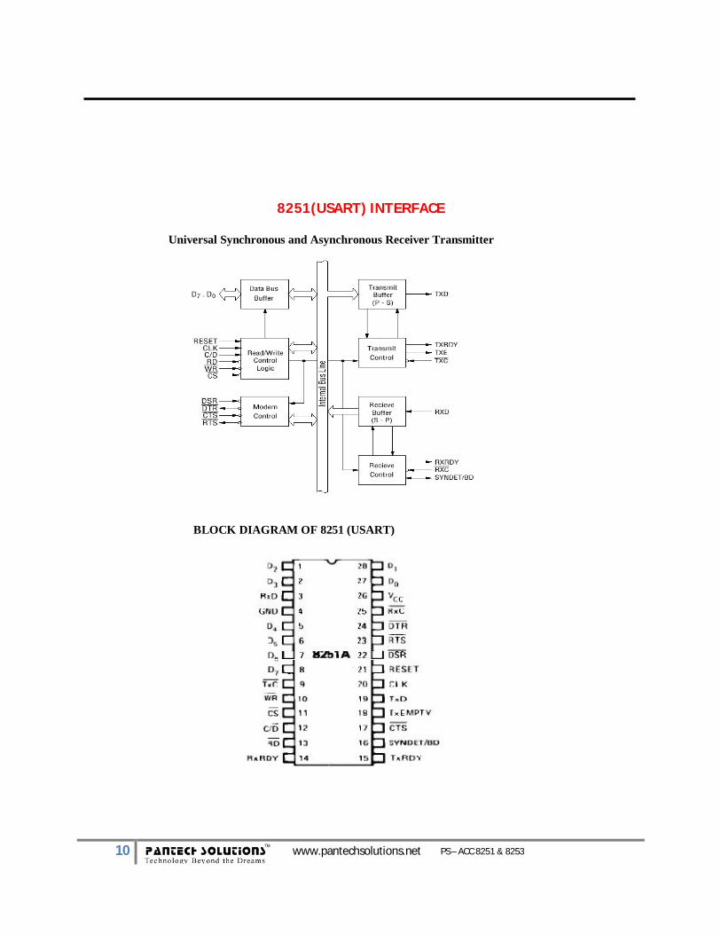
8251(USART) INTERFACE
Universal Synchronous and Asynchronous Receiver Transmitter
BLOCK DIAGRAM OF 8251 (USART)

11
PS – ACC 8251 & 8253 www.pantechsolutions.net
PIN DIAGRAM OF 8251
The 8251 functional configuration is programmed by software. Operation between the 8251 and a CPU is executed by program control. Table 1 shows the operation between a CPU and the device.
STATUS WORD:
D7 D6 D5 D4 D3 D2 D1 D0
DSR SYNDET/BD FE OE PE TXEMPTY RXRDY TXRDY
TXRDY: TXRDY status bit has different meanings from the TXRDY output pin. The former is not conditioned by CTS & TxEN; the latter is conditioned by both CTS & TXEN (i.e) TXRDY status bit = DB buffer empty, TXRDY pin out = DB buffer empty. (CTS-0). (TXEN-1). RXRDY: Receiver Ready, this bit indicates that the 8251A contains a character that is ready to be input to the CPU. TXEMPTY: Transmitter Empty, when the 8251A has no character to transmit this bit will go high. PE: Parity Error, the PE flag is set when a parity error is detected. It is reset by the ER bit of the command instruction. PE does not inhibit operation of the 8251A. OE: Overrun Error. The OE flag is set when the CPU does not read character before the next one becomes available. OE is reset by the ERbit of the command instruction. OE does not inhibit the operation of8251A however the previously overrun character is lost. FE: Framing error (ASYNC only), the FE flag is set when a valid stop bites not detected at end of every character. It is reset by the ER BIT of the command instruction. FE does not inhibit the operation of 8251A. SYNDET: SYNC Detect. This pin is used in synchronous mode for syndet and issued in asynchronous mode for break detect. DSR: Data Set Ready, indicates that the DSR is at zero level.
COMMAND WORD
D7 D6 D5 D4 D3 D2 D1 D0
DSR SYNDET FE OE PE TXEMPTY RXRDY TXRDY
0 0 0 0 0 1 0 0
Txempty (D2) Transmitter Empty, when the 8251A has no character to transmit this bit will go high.
Gives a status word of 00000100 = 04(Hex).
12
PS – ACC 8251 & 8253 www.pantechsolutions.net
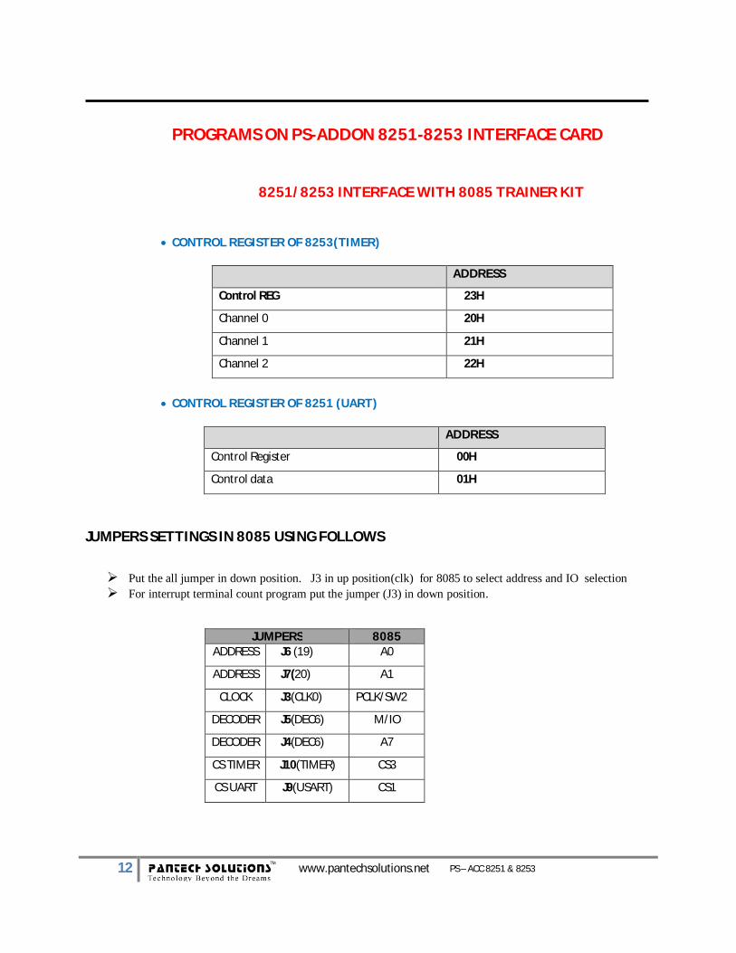
PROGRAMS ON PS-ADDON 8251-8253 INTERFACE CARD
8251/8253 INTERFACE WITH 8085 TRAINER KIT
CONTROL REGISTER OF 8253(TIMER)
ADDRESS
Control REG 23H
Channel 0 20H
Channel 1 21H
Channel 2 22H
CONTROL REGISTER OF 8251 (UART)
ADDRESS
Control Register 00H
Control data 01H
JUMPERS SETTINGS IN 8085 USING FOLLOWS
Put the all jumper in down position. J3 in up position(clk) for 8085 to select address and IO selection For interrupt terminal count program put the jumper (J3) in down position.
JUMPERS 8085 ADDRESS J6 (19) A0
ADDRESS J7(20) A1
CLOCK J3(CLK0) PCLK/SW2
DECODER J5(DEC6) M/IO
DECODER J4(DEC6) A7
CS TIMER J10(TIMER) CS3
CS UART J9(USART) CS1
13
PS – ACC 8251 & 8253 www.pantechsolutions.net
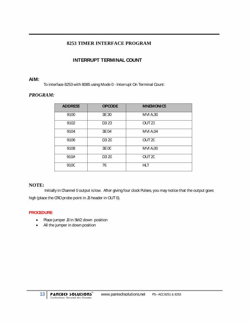
8253 TIMER INTERFACE PROGRAM
INTERRUPT TERMINAL COUNT
AIM:
To interface 8253 with 8085 using Mode 0 - Interrupt On Terminal Count: PROGRAM:
NOTE: Initially in Channel 0 output is low. After giving four clock Pulses, you may notice that the output goes
high (place the CRO probe point in J3 header in OUT 0).
PROCEDURE
Place jumper J3 in SW2 down position All the jumper in down position
ADDRESS OPCODE MNEMONICS
9100 3E 30 MVI A,30
9102 D3 23 OUT 23
9104 3E 04 MVI A,04
9106 D3 20 OUT 20
9108 3E 00 MVI A,00
910A D3 20 OUT 20
910C 76 HLT
14
PS – ACC 8251 & 8253 www.pantechsolutions.net
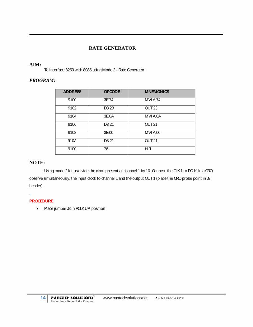
RATE GENERATOR AIM:
To interface 8253 with 8085 using Mode 2 - Rate Generator:
PROGRAM:
NOTE:
Using mode 2 let us divide the clock present at channel 1 by 10. Connect the CLK 1 to PCLK. In a CRO
observe simultaneously, the input clock to channel 1 and the output OUT 1 (place the CRO probe point in J3
header).
.
PROCEDURE
Place jumper J3 in PCLK UP position
ADDRESS OPCODE MNEMONICS
9100 3E 74 MVI A,74
9102 D3 23 OUT 23
9104 3E 0A MVI A,0A
9106 D3 21 OUT 21
9108 3E 00 MVI A,00
910A D3 21 OUT 21
910C 76 HLT

15
PS – ACC 8251 & 8253 www.pantechsolutions.net
SQURE WAVE GENERATOR
AIM:
To Interface 8253 With 8085mode 3 - Square Waves Generator.
PROGRAM:
Mode 3 Channel 0 LSB of count MSB of count
NOTE:
To generate a square wave of frequency 270 KHz at OUT2, CLK 0 of 8253 is connected to PCLK of frequency 3 MHz PROCEDURE:
Place jumper J3 in PCLK position
CALCULATION:
Square wave frequency ₌
₌
₌ 0.272 MHz ₌ 272 KHz Where, PCLK → 3 MHz Count → 0x0B [(11)10]
ADDRESS OPCODE MNEMONICS
9100 3E 36 MVI A,36
9102 D3 23 OUT 23
9104 3E 0B MVI A,0B
9106 D3 22 OUT 22
9108 3E 00 MVI A,00
910A D3 22 OUT 22
910C 76 HLT

16
PS – ACC 8251 & 8253 www.pantechsolutions.net
8251 UART INTERFACE PROGRAM
.
SERIAL COMMUNICATION WITH PC AND 8085 KIT AIM:
To Interface 8251 with 8085, Communication with 8253/8251 and PC.
PROGRAM:
ADDRESS OPCODE MNEMONICS
9100 3E B6 MVI A,B6
9102 D3 23 OUT 23
9104 3E 40 MVI A,40
9106 D3 22 OUT 22
9108 3E 01 MVI A,01
910A D3 22 OUT 22
910C 0E 05 RELOD : MVI C,05
910E DB 01 CHECK: IN 01
9110 E6 04 ANI 04
9112 CA 0E 91 JZ CHECK
9115 21 00 92 START : LXI H,9200
9118 06 0C MVI B,0C
911A 7E REPET: MOV A,M
911B D3 00 OUT 00
911D 11 03 03 LXI D,0303
9120 00 DELAY: NOP
9121 1B DCX D
9122 7B MOV A,E
9123 B2 ORA D
9124 C2 20 91 JNZ DELAY
9127 23 INX H
9128 05 DCR B
9129 C2 1A 91 JNZ REPET
912C C3 15 91 JMP START

17
PS – ACC 8251 & 8253 www.pantechsolutions.net
ORG 9200H 9200 41 42 43 44 DB 48H, 45H,4CH,4CH 9204 45 46 47 48 DB 4FH,2DH,38H,30H 9208 38 35 0A 0D DB 38H,35H,0AH,0DH END
PROCEDURE:
Place jumper J3 in PCLK up position
Connect the serial 9 to 9 cable interface card to pc (FEMALE TO MALE)
Enter the program
Set the baud rate value 9600. Execute the G9100 program
Pc in through the hyper terminal window set the baud rate same 9600 value
Get the output “HELLO-8085” message will be displayed on HyperTerminal
912F FE 3F CPI 3F
9131 C2 0C 91 JNZ RELOD
9134 0D DCR C
9135 C2 0E 91 JNZ CHECK
9138 CF RST 1

18
PS – ACC 8251 & 8253 www.pantechsolutions.net
SERIAL COMMUNICATION BETWEEN TWO MICROPROCESSORS
PROCEDURE:
Place jumper J3 in PCLK up position in both
Connect the serial 9 to 9 cable transmitter kit to receiver kit (MALE TO MALE)
Enter the program. After Set the baud rate value 9600 both trainer kit
First Receiver program execution again transmitter program execution
Then both 8085 trainer kit press reset switch. Receiver program location 9200 we got the output
AIM:
Serial communication between two microprocessors using 8085 trainer kit in Transmitter & Receiver follows
PROGRAM IN TRANSMITTER:
ADDRESS OPCODE MNEMONICS
9100 21 00 92 LXI H,9200
9103 3E B6 MVI A,B6
9105 D3 13 OUT 13
9107 3E 40 MVI A,40
9109 D3 12 OUT 12
910B 3E 01 MVI A,01
910D D3 12 OUT 12
910F 0E 05 RELOD : MVI C,05
9111 DB 01 CHECK : IN 01
9113 E6 04 ANI 04
9115 CA 11 91 JZ CHECK
9118 7E MOV A,M
9119 D3 00 OUT 00
911B 23 INX H
911C FE 3F CPI 3F
911E C2 0F 91 JNZ RELOD
9121 0D DCR C
9122 C2 11 91 JNZ CHECK
9125 CF RST 1

19
PS – ACC 8251 & 8253 www.pantechsolutions.net
ORG 9200H
9200 01 02 03 04 DB 01H, 02H,03H,04H
PROGRAM IN RECEIVER: OUTPUT: Receiver date in address 9200 location
9200 01 02 03 04
ADDRESS OPCODE MNEMONICS
9100 21 00 95 LXI H,9200
9103 3E B6 MVI A,B6
9105 D3 23 OUT 23
9107 3E 40 MVI A,40
9109 D3 22 OUT 22
910B 3E 01 MVI A,01
910D D3 22 OUT 22
910F 0E 05 RELOD : MVI C,05
9111 DB 01 CHECK : IN 01
9113 E6 02 ANI 04
9115 CA 11 91 JZ CHECK
9118 DB 00 IN 00
911A 77 MOV M,A
911B 23 INX H
911C FE 3F CPI 3F
911E C2 0F 91 JNZ RELOD
9121 0D DCR C
9122 C2 11 91 JNZ CHEAK
9125 CF RST 1
9126 CF RST 1
20
PS – ACC 8251 & 8253 www.pantechsolutions.net
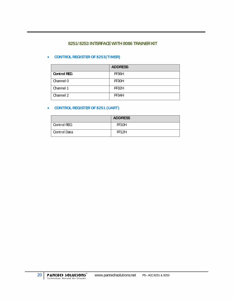
8251/8253 INTERFACE WITH 8086 TRAINER KIT
CONTROL REGISTER OF 8253(TIMER)
ADDRESS
Control REG FF36H
Channel 0 FF30H
Channel 1 FF32H
Channel 2 FF34H
CONTROL REGISTER OF 8251 (UART)
ADDRESS
Control REG FF10H
Control Data FF12H
21
PS – ACC 8251 & 8253 www.pantechsolutions.net
PROGRAM 1: AIM: To interface 8253 with 8086 using Mode 0 - Interrupt On Terminal Count:
NOTE: Initially in Channel 0 output is low. After giving four clock Pulses, you may notice that the output goes high
(place the CRO probe point in J3 header in OUT 0).
PROCEDURE:
Place jumper J3 in SW2 position
ADDRESS OPCODE MNEMONICS
1100 B0 30 MOV AL,30
1102 BA 36 FF MOV DX,FF36
1105 EE OUT DX,AL
1106 B0 04 MOV AL,04
1108 BA 30 FF MOV DX,FF30
110B EE OUT DX,AL
110C B0 00 MOV AL,00
110E BA 30 FF MOV DX,FF30
1111 EE OUT DX,AL
1112 F4 HLT

22
PS – ACC 8251 & 8253 www.pantechsolutions.net
PROGRAM 2: AIM: To interface 8253 with 8086 using Mode 2 - Rate Generator:
NOTE: Using mode 2 let us divide the clock present at channel 1 by 10. Connect the CLK 1 to PCLK. In a CRO
observe simultaneously, the input clock to channel 1 and the output OUT 1 (place the CRO probe point in J3 header
in OUT1).
PROCEDURE
Place jumper J3 in PCLK position
ADDRESS OPCODE MNEMONICS
1100 B0 30 MOV AL,74
1102 BA 36 FF MOV DX,FF36
1105 EE OUT DX,AL
1106 B0 04 MOV AL,0A
1108 BA 30 FF MOV DX,FF32
110B EE OUT DX,AL
110C B0 00 MOV AL,00
110E BA 30 FF MOV DX,FF32
1111 EE OUT DX,AL
1112 F4 HLT

23
PS – ACC 8251 & 8253 www.pantechsolutions.net
PROGRAM 3 AIM: To interface 8253 with 8086 using mode 3 - square waves generator:
NOTE: To generate a square wave of frequency 270 KHz at OUT2, CLK 0 of 8253 is connected to PCLK of frequency 3 MHz PROCEDURE
Place jumper J3 in PCLK position CALCULATION Square wave frequency ₌
₌
.
₌ 0.280 MHz ₌ 280 KHz Where, PCLK → 3.1 MHz Count → 0x0B [(11)10]
ADDRESS OPCODE MNEMONICS
1100 B0 30 MOV AL,36
1102 BA 36 FF MOV DX,FF36
1105 EE OUT DX,AL
1106 B0 04 MOV AL,0B
1108 BA 30 FF MOV DX,FF30
110B EE OUT DX,AL
110C B0 00 MOV AL,00
110E BA 30 FF MOV DX,FF30
1111 EE OUT DX,AL
1112 F4 HLT

24
PS – ACC 8251 & 8253 www.pantechsolutions.net
PROGRAM 4 AIM: Serial communication between two microprocessors using 8086 trainer kit TRANSMITTER PROGRAM:
ADDRESS OPCODE MNEMONICS
1100 BE 00 12 MOV SI,1200
1103 B0 B6 MOV BL,B6
1105 BA 36 FF MOV DX,FF36
1108 EE OUT DX,AL
1109 B0 40 MOV AL,40
110B BA 34 FF MOV DX,FF34
110E EE OUT DX,AL
110F B0 01 MOV AL,01
1111 BA 34 FF MOV DX,FF34
1114 EE OUT DX,AL
1115 B1 05 RELOD : MOV CL,05
1117 BA 12 FF CHECK : MOV DX,FF12
111A EC IN AL,DX
111B 24 04 AND AL,04
111D 74 F8 JZ CHECK
111F 8A 04 MOV AL,[SI]
1121 BA 10 FF MOV DX,FF10
1124 EE OUT DX,AL
1125 46 INC SI
1126 3C 3F CMP AL,3F
1128 75 EB JNZ RELOD
112A FE C9 DEC CL

25
PS – ACC 8251 & 8253 www.pantechsolutions.net
RECEIVER PROGRAM:
112C 75 E9 JNZ CHECK
112E CC INT 03
ADDRESS OPCODE MNEMONICS
1100 BE 00 15 MOV SI,1500
1103 B0 B6 MOV BL,B6

26
PS – ACC 8251 & 8253 www.pantechsolutions.net
1105 BA 36 FF MOV DX,FF36
1108 EE OUT DX,AL
1109 B0 40 MOV AL,40
110B BA 34 FF MOV DX,FF34
110E EE OUT DX,AL
110F B0 01 MOV AL,01
1111 BA 34 FF MOV DX,FF34
1114 EE OUT DX,AL
1115 B1 05 RELOD : MOV CL,05
1117 BA 12 FF CHECK : MOV DX,FF12
111A EC IN AL,DX
111B 24 02 AND AL,02
111D 74 F8 JZ CHECK
111F BA 10 FF MOV DX,FF10
1122 EC IN AL,DX
1123 88 04 MOV [SI],AL
1125 46 INC SI
1126 3C 3F CMP AL,3F
1128 75 EB JNZ RELOD
112A FE C9 DEC CL
112C 75 E9 JNZ CHECK
112E CC INT 03
112F CC INT 03

27
PS – ACC 8251 & 8253 www.pantechsolutions.net
PROCEDURE:
Place jumper J3 in PCLK position
Connect the two Interface card serial ports with the RS232C cable (female to female).
Transmitting the input location 1200H.
At the transmitter end execute the program starting from location 1100H.
At the receiver end execute the program starting from location 1100h.
Will be get the output location 1500h
TRANSMITTER INPUT RECEIVER OUTPUT Address opcode Address opcode 1200 27 1500 27

28
PS – ACC 8251 & 8253 www.pantechsolutions.net
8251/8253 INTERFACE WITH 8051 TRAINER KIT
1) CONTROL REGISTER OF 8253(TIMER)
ADDRESS
Control REG 4086H
Channel 0 4080H
Channel 1 4082H
Channel 2 4084H
2) CONTROL REGISTER OF 8251 (UART)
ADDRESS
Control REG 40A0H
Control Data 40A2H

29
PS – ACC 8251 & 8253 www.pantechsolutions.net
PROGRAM1: AIM: To interface ps-8251/8253 with 8051 trainer kit to generate Interrupt on Terminal Count Using 8253
NOTE: Connect CLKO of 8253 to the SW2 position (jumper j3)
OUTPUT: Execute the program. Observe the output of channel 0. After giving six clock pulses, output goes high,
view the output in CRO (place the probe point in J3 header in OUT 0).
ADDRESS OPCODE MNEMONICS
9100 74 30 MOV A,#30
9102 90 40 80 MOV DPTR,#4086
9105 F0 MOVX @DPTR,A
9106 74 30 MOV A,#04
9108 90 40 80 MOV DPTR,#4080
910B F0 MOV X @DPTR,A
910C 74 00 MOV A,#00
910E 90 40 80 MOV DPTR,#4080
9111 F0 MOVX @DPTR,A
9112 80 FE SJMP 9112

30
PS – ACC 8251 & 8253 www.pantechsolutions.net
PROGRAM 2: AIM: To interface ps-8251/8253 with 8051 trainer kit to Design A Rate Generator Using 8253
OUTPUT: In CRO observe the input clock to channel 1 and the output OUT1 (place the CRO probe point in J3 header). Please make sure that CLK 1 is connected to PCLK. In a CRO observe the input clock to channel 1 and the output OUT 1.
ADDRESS OPCODE MNEMONICS
9100 74 30 MOV A,#74
9102 90 40 80 MOV DPTR,#4086
9105 F0 MOVX @DPTR,A
9106 74 30 MOV A,#0A
9108 90 40 80 MOV DPTR,#4082
910B F0 MOV X @DPTR,A
910C 74 00 MOV A,#00
910E 90 40 80 MOV DPTR,#4082
9111 F0 MOVX @DPTR,A
9112 80 FE SJMP 9112

31
PS – ACC 8251 & 8253 www.pantechsolutions.net
PROGRAM 3: AIM: To design A Square Waves Generator Using 8253
OUTPUT: In CRO observe the input clock to channel 0 and the output OUT0 (place the CRO probe point in J3 header). .
ADDRESS OPCODE MNEMONICS
9100 74 30 MOV A,#36
9102 90 40 80 MOV DPTR,#4086
9105 F0 MOVX @DPTR,A
9106 74 30 MOV A,#0B
9108 90 40 80 MOV DPTR,#4080
910B F0 MOV X @DPTR,A
910C 74 00 MOV A,#00
910E 90 40 80 MOV DPTR,#4080
9111 F0 MOVX @DPTR,A
9112 80 FE SJMP 9112
Related Documents