2018 IEEE TRANSACTIONS ON POWER ELECTRONICS, VOL. 23, NO. 4, JULY 2008 Proximate Time-Optimal Digital Control for Synchronous Buck DC–DC Converters Vahid Yousefzadeh, Member, IEEE, Amir Babazadeh, Student Member, IEEE, Bhaskar Ramachandran, Eduard Alarcón, Member, IEEE, Lucy Pao, Senior Member, IEEE, and Dragan Maksimovic ´ , Senior Member, IEEE Abstract—This paper introduces an approach to near time- optimal control for synchronous buck dc–dc converters. The pro- posed proximate time-optimal digital (PTOD) controller is a com- bination of a constant-frequency pulsewidth modulation (PWM) controller employing a linear PID compensator close to a reference point, and a linear or nonlinear switching surface controller (SSC) away from the reference, together with smooth transitions between the two. A hybrid capacitor current estimator enables switching surface evaluation and eliminates the need for current sensing. The SSC, which is implemented as a small Verilog HDL module, can be easily added to an existing digital PWM controller to construct the PTOD controller. In steady state, the controller operates exactly the same as a standard constant-frequency PWM controller with a linear PID compensator. Simulation and experimental results are shown for a 6.5 V-to-1.3 V, 10 A synchronous buck converter. Index Terms—Boundary control, dc–dc converters, digital con- trol, switching surface control, time-optimal control. I. INTRODUCTION I N the field of control of switched-mode dc–dc power con- verters, such as the synchronous buck voltage regulator in Fig. 1, most commonly adopted are standard frequency domain design techniques based on approximate linear time-invariant averaged small-signal models [1], [2]. Starting with the seminal work in [3], it has been recognized that directly taking into ac- count the switching nature of the power stage, and operating with large-signal instantaneous state variables to provide the on-off control action accordingly, can result in improved dynamic re- sponses. The switching surface control [3] and related approaches have also been designated as boundary or geometric control [4]. One case of special interest of the switching surface control re- sults in minimum-time responses, as in the example waveforms shown in Fig. 2(a). By taking into account the converter state tra- jectories in the two possible switched states, a switching surface can be derived that naturally provides an on/off sequence that Manuscript received July 2, 2007; revised September 20, 2007. Published July 7, 2008 (projected). This work was supported by the Colorado Power Electronics Center (CoPEC), by a Grant provided by AGAUR, Generalitat de Catalunya, Project TEC2004-05608-C02-01 from the Spanish MCYT, and by EU FEDER F. Recommended for publication by Associate Editor C. K. Tse. V. Yousefzadeh is with Texas Instruments, Dallas, TX 75243 USA. A. Babazadeh, L. Pao, and D. Maksimovic ´ are with the Electrical and Com- puter Engineering Department, University of Colorado at Boulder, Boulder, CO 80309-0425 USA (e-mail: [email protected]; [email protected]; [email protected]). B. Ramachandran is with National Semiconductor Corporation, Fort Collins, CO 80525 USA. E. Alarcón is with the Department of Electronic Engineering, Technical Uni- versity of Catalunya, Barcelona, Spain. Color versions of one or more of the figures in this paper are available at http://ieeexplore.ieee.org. Digital Object Identifier 10.1109/TPEL.2008.924843 Fig. 1. Synchronous buck dc–dc voltage regulator. Prototype example: V, H, F, switching frequency kHz, V, A. results in the fastest, i.e., time-optimal rejection of large-signal disturbances, as illustrated in the state diagram of Fig. 2(b), which corresponds to the waveforms in Fig. 2(a). Using con- verter trajectories as switching surfaces for the case of infinite load is discussed in [5], whereas in [6], given the complexity of the theoretical switching surface, the behavior of different approximations is explored. The nonlinear state-feedback that provides time-optimal control can also be derived from an en- ergy transfer approach, as discussed in [7] and more recently in [8]. With the advent of recent applications with more stringent specifications in terms of regulator settling time, various approx- imations to time-optimal control have recently been proposed, e.g., in [9]–[11], where time-optimal control is described in terms of boundary control and revisited for the buck converter. Reference [12] reexamines the switching-surface time-optimal control and derives analytical equations for the optimal case, similarly to [5]. Recent works in [13]–[15] provide a com- prehensive account of geometric control principles, including limits of time-optimal control for switching converters. In the field of general control theory, the fundamentals of time-optimal control, which are directly related to the use of Pontryagin’s principle, have been studied extensively [16]. Un- fortunately, it has been recognized that ideal time-optimal con- trol may be impractical because of the sensitivity to parameter variations, and unmodeled dynamics [17]. To address this issue, a concept of proximate time-optimal (PTO) control has been proposed [18]–[21] and successfully applied in, for example, disk-drive head positioning. The main underlying idea considers saturating the control action to facilitate near-time-optimal re- sponse to large-signal disturbances and smoothly switching the controller to a standard continuous-time control action in the vicinity of steady state. By combining a time-optimal and a linear controller, it is possible to achieve the favorable proper- ties of both types, namely, fast large-signal transient responses, 0885-8993/$25.00 © 2008 IEEE Authorized licensed use limited to: Univ of Calif Berkeley. Downloaded on November 3, 2008 at 14:20 from IEEE Xplore. Restrictions apply.

Welcome message from author
This document is posted to help you gain knowledge. Please leave a comment to let me know what you think about it! Share it to your friends and learn new things together.
Transcript

2018 IEEE TRANSACTIONS ON POWER ELECTRONICS, VOL. 23, NO. 4, JULY 2008
Proximate Time-Optimal Digital Control forSynchronous Buck DC–DC Converters
Vahid Yousefzadeh, Member, IEEE, Amir Babazadeh, Student Member, IEEE, Bhaskar Ramachandran,Eduard Alarcón, Member, IEEE, Lucy Pao, Senior Member, IEEE, and Dragan Maksimovic, Senior Member, IEEE
Abstract—This paper introduces an approach to near time-optimal control for synchronous buck dc–dc converters. The pro-posed proximate time-optimal digital (PTOD) controller is a com-bination of a constant-frequency pulsewidth modulation (PWM)controller employing a linear PID compensator close to a referencepoint, and a linear or nonlinear switching surface controller (SSC)away from the reference, together with smooth transitions betweenthe two. A hybrid capacitor current estimator enables switchingsurface evaluation and eliminates the need for current sensing. TheSSC, which is implemented as a small Verilog HDL module, can beeasily added to an existing digital PWM controller to construct thePTOD controller. In steady state, the controller operates exactlythe same as a standard constant-frequency PWM controller witha linear PID compensator. Simulation and experimental resultsare shown for a 6.5 V-to-1.3 V, 10 A synchronous buck converter.
Index Terms—Boundary control, dc–dc converters, digital con-trol, switching surface control, time-optimal control.
I. INTRODUCTION
I N the field of control of switched-mode dc–dc power con-verters, such as the synchronous buck voltage regulator in
Fig. 1, most commonly adopted are standard frequency domaindesign techniques based on approximate linear time-invariantaveraged small-signal models [1], [2]. Starting with the seminalwork in [3], it has been recognized that directly taking into ac-count the switching nature of the power stage, and operating withlarge-signal instantaneous state variables to provide the on-offcontrol action accordingly, can result in improved dynamic re-sponses.Theswitchingsurfacecontrol [3]andrelatedapproacheshave also been designated as boundary or geometric control [4].
One case of special interest of the switching surface control re-sults in minimum-time responses, as in the example waveformsshown in Fig. 2(a). By taking into account the converter state tra-jectories in the two possible switched states, a switching surfacecan be derived that naturally provides an on/off sequence that
Manuscript received July 2, 2007; revised September 20, 2007. PublishedJuly 7, 2008 (projected). This work was supported by the Colorado PowerElectronics Center (CoPEC), by a Grant provided by AGAUR, Generalitat deCatalunya, Project TEC2004-05608-C02-01 from the Spanish MCYT, and byEU FEDER F. Recommended for publication by Associate Editor C. K. Tse.
V. Yousefzadeh is with Texas Instruments, Dallas, TX 75243 USA.A. Babazadeh, L. Pao, and D. Maksimovic are with the Electrical and Com-
puter Engineering Department, University of Colorado at Boulder, Boulder,CO 80309-0425 USA (e-mail: [email protected]; [email protected];[email protected]).
B. Ramachandran is with National Semiconductor Corporation, Fort Collins,CO 80525 USA.
E. Alarcón is with the Department of Electronic Engineering, Technical Uni-versity of Catalunya, Barcelona, Spain.
Color versions of one or more of the figures in this paper are available athttp://ieeexplore.ieee.org.
Digital Object Identifier 10.1109/TPEL.2008.924843
Fig. 1. Synchronous buck dc–dc voltage regulator. Prototype example: V =
6:5 V, L = 1 �H, C = 288 �F, switching frequency f = 780 kHz, V =
1:3 V, I = 0 � 10 A.
results in the fastest, i.e., time-optimal rejection of large-signaldisturbances, as illustrated in the state diagram of Fig. 2(b),which corresponds to the waveforms in Fig. 2(a). Using con-verter trajectories as switching surfaces for the case of infiniteload is discussed in [5], whereas in [6], given the complexityof the theoretical switching surface, the behavior of differentapproximations is explored. The nonlinear state-feedback thatprovides time-optimal control can also be derived from an en-ergy transfer approach, as discussed in [7] and more recently in[8]. With the advent of recent applications with more stringentspecifications in terms of regulator settling time, various approx-imations to time-optimal control have recently been proposed,e.g., in [9]–[11], where time-optimal control is described interms of boundary control and revisited for the buck converter.Reference [12] reexamines the switching-surface time-optimalcontrol and derives analytical equations for the optimal case,similarly to [5]. Recent works in [13]–[15] provide a com-prehensive account of geometric control principles, includinglimits of time-optimal control for switching converters.
In the field of general control theory, the fundamentals oftime-optimal control, which are directly related to the use ofPontryagin’s principle, have been studied extensively [16]. Un-fortunately, it has been recognized that ideal time-optimal con-trol may be impractical because of the sensitivity to parametervariations, and unmodeled dynamics [17]. To address this issue,a concept of proximate time-optimal (PTO) control has beenproposed [18]–[21] and successfully applied in, for example,disk-drive head positioning. The main underlying idea considerssaturating the control action to facilitate near-time-optimal re-sponse to large-signal disturbances and smoothly switching thecontroller to a standard continuous-time control action in thevicinity of steady state. By combining a time-optimal and alinear controller, it is possible to achieve the favorable proper-ties of both types, namely, fast large-signal transient responses,
0885-8993/$25.00 © 2008 IEEE
Authorized licensed use limited to: Univ of Calif Berkeley. Downloaded on November 3, 2008 at 14:20 from IEEE Xplore. Restrictions apply.

YOUSEFZADEH et al.: PROXIMATE TIME-OPTIMAL DIGITAL CONTROL 2019
Fig. 2. (a) Waveforms illustrating time-optimal response to a 0–10 A step loadtransient in the converter of Fig. 1(b). State plane diagram for the 0–10 A stepload transient, a linear switching surface, and a nonlinear switching surface.
precise control in steady state, and overall robustness againstparameter variations and unmodeled dynamics. The approachpresented in this paper is inspired by the PTO ideas and results.
In addition to robustness issues addressed in control theory,a disadvantage that has hitherto precluded widespread use oftime-optimal control for dc–dc converters has to do with con-troller implementation difficulties. In analog controller imple-mentations, the challenges of implementing a nonlinear con-trol law are notable. For example, current-mode circuit tech-niques to implement squaring functions are proposed in [22],whereas fuzzy approximation techniques are used to synthesizethe multi-input nonlinear switching surface in [23].
With advances in digital control for high-frequency switched-mode converters (e.g., [24], [25]), new possibilities arise to
consider practical realizations of more advanced control ap-proaches. In particular, Section II briefly reviews previouslyreported approaches to digital implementation of near time-optimal or nonlinear control for dc–dc converters [26]–[32].Following this review, an argument is made that proximatetime-optimal digital (PTOD) control proposed in this paper,based on a combination of linear or nonlinear switching surfaceand standard linear (e.g., PID) control can have advantagesin dc–dc voltage regulators where arbitrary load disturbancesand realistic component tolerances must be taken into account.An approach to capacitor current estimation, which is a keycomponent of the switching surface controller described inthis paper, is introduced in Section III. Section IV describesthe complete PTOD controller. Simulation and experimentalresults for a 6.5–1.3 V, 10 A synchronous buck point-of-loadconverter with the PTOD controller are described in Section V.Sections VI summarizes the conclusions.
II. DIGITAL TIME-OPTIMAL CONTROL
IMPLEMENTATION APPROACHES
In this section, the example in Figs. 1 and 2 is used to reviewand discuss approaches to digital realization of near-time op-timal control for dc–dc converters.
A. Programmed On/Off Times
Assuming a specific type of load transient (e.g., a step in load),the times , and corresponding to time-optimalresponse can be found in terms of operating conditions and cir-cuit parameter values using the output capacitor charge balanceapproach [26]–[28]. This approach requires implementationof relatively complex computations and also relies on precisereal-time inductor current sensing. A combined linear PID and anonlinear controller with pre-computed on/off times stored in alook-up-table for a limited set of possible step load transients isdescribed in [30]. The approach presented in [31] also combinesa linear PID controller with a near-time-optimal controller intransients. Based on detecting the valley (or peak) in the outputvoltage waveform, the on/off control is executed with the times
and stored in a look-up table. This approach has advan-tages of requiring no current sensing, and having a relativelysimple realization based on continuous-time DSP concepts.
B. Switching Surface
As opposed to computing or programming the on/off timesto achieve fast large-signal transient response for a specific typeof load transient, a switching surface controller (SSC) is basedon sensing (or estimating) converter states . The switch on/offposition, i.e., the switch control signal is then determined from
(1)
where defines the switching surface: the on-to-offswitching occurs at the time the converter state trajectorycrosses the switching surface. For the case when the statesare the capacitor voltage and the capacitor current, Fig. 2(b)shows examples of a linear switching surface and a non-linearswitching surface. As discussed in the introductory section,it has been shown that the switching surface can be designed
Authorized licensed use limited to: Univ of Calif Berkeley. Downloaded on November 3, 2008 at 14:20 from IEEE Xplore. Restrictions apply.

2020 IEEE TRANSACTIONS ON POWER ELECTRONICS, VOL. 23, NO. 4, JULY 2008
to enable near-time-optimal responses for the important classof step load transients. Even more importantly, a feedbackmechanism is applied at all times, and the controller based onthe same switching surface can be shown to result in stable,well-behaved dynamic responses in general. This advantageis very significant in dc–dc converter applications where thenature of load transients is generally not known in advance.
The main difficulty associated with implementing (1) in a dig-ital controller is related to sensing or estimation of the converterstates. While the output voltage sensing is necessary in any con-troller realization, it is desirable to consider practical estimationmethods to remove the need for precision current sensing. Inparticular, capacitor current sensing is completely impracticalin many cases. The next section introduces an approach to ca-pacitor current estimation.
III. CAPACITOR CURRENT ESTIMATION
Consider the case when the output voltage erroris sampled by an A/D converter having a least significant
bit (LSB) resolution , at the rate , whereis the switching frequency and is the oversampling rate.
A very basic finite-difference estimator for the capacitor currentis given by
(2)
Taking the -transform of (2) results in
(3)
The estimation filter transfer function can bewritten as
(4)
Note that at relatively low frequencies, closely approxi-mates the ideal analog derivative action except for adelay of , which can be neglected if the oversamplingrate is high. Fig. 3(b) shows an example of successful capacitorcurrent estimation using (2), assuming , and a veryhigh resolution A/D, . Unfortunately, the estimator(2) is highly susceptible to switching noise in the sensed outputvoltage, and to quantization errors, as illustrated in Fig. 3(c)for mV: the effective resolution in is very low.Taking advantage of the oversampling, low-pass filtering ofcan partially alleviate the problem. For example, applying amoving-average filter of order to in (2) yields a filteredfinite-difference estimator
(5)
Similar to (4), the estimation filter transfer functioncan be written as
(6)
Fig. 3. (a) Output voltage waveform during a step-load-transient; (b)-(e) ca-pacitor current i , and capacitor current estimates based on: (b) finite-differenceestimator using very high-resolution voltage A/D converter, (c) finite-differenceestimator using relatively low-resolution voltage A/D converter, (d) filtered fi-nite-difference estimator, and (e) hybrid estimator.
which shows that (5) approximates ideal analog differentiation,but with a delay of . In digital hardware, the filteredfinite-difference estimator is executed as
(7)
One may note that (7) reduces to (2) for . Fig. 3(d) illus-trates the estimation performance of (7). Although an improve-ment in effective resolution by a factor of can be observed, arealization of (1) with the capacitor current estimator (7) would
Authorized licensed use limited to: Univ of Calif Berkeley. Downloaded on November 3, 2008 at 14:20 from IEEE Xplore. Restrictions apply.
YOUSEFZADEH et al.: PROXIMATE TIME-OPTIMAL DIGITAL CONTROL 2021
still be significantly affected by the quantization errors, espe-cially around zero (i.e., around the switching), and by the largerdelay of due to moving-average filtering.
Let us consider an integral estimator of the ac component ofthe inductor current as an alternative approach. Since
, in the buck converter of Fig. 1, the inductor current slopesare and in the two switchpositions, and , respectively. Since ,assuming a known initial condition, an integral current estimatorcan be constructed as
ifif (8)
which is not subject to quantization errors. It has been shownthat (8) can be combined with a low-resolution current sensingA/D and a low-resolution D/A converter to yield a high-reso-lution estimate of the inductor current [40]. Unfortunately, theapproach based on (8) is not suitable for detecting fast changesin the capacitor current. A hybrid estimator , which is a com-bination of (7) and (8) is proposed to overcome these difficulties.Initially, . Then, taking into account the delay of
in the estimate (7), an initial value for the integralestimator (8) is found as
ifif
(9)
at the point where in (7) reaches a peak value, e.g., after afast load transient.
From this point on, the integral estimator (8) is employed,. To account for arbitrary load disturbances, a
reset of the initial value in (8) can be performed based on (9)whenever a large (e.g., more than LSB) difference betweenand is detected.
Fig. 3(e) shows an example of the hybrid estimator perfor-mance. Immediately after the step load transient, the hybrid es-timator provides a reliable indication of the direction and size ofthe load change, which is sufficient for the SSC operation whenthe state trajectory is away from the switching surface. Then,importantly, an accurate, high-resolution capacitor current esti-mate is available around the points where the state trajectory iscrossing the switching surface as required in the implementa-tion of the SSC law (1).
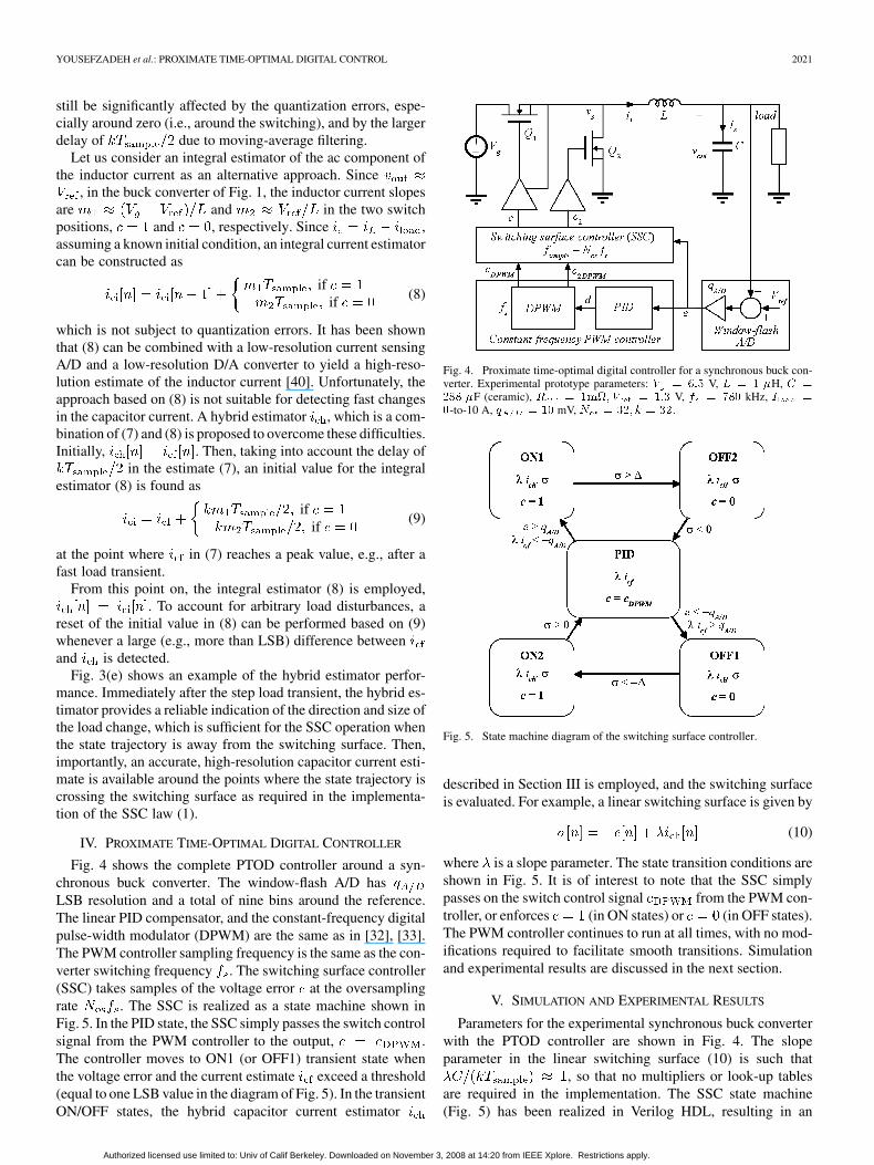
IV. PROXIMATE TIME-OPTIMAL DIGITAL CONTROLLER
Fig. 4 shows the complete PTOD controller around a syn-chronous buck converter. The window-flash A/D hasLSB resolution and a total of nine bins around the reference.The linear PID compensator, and the constant-frequency digitalpulse-width modulator (DPWM) are the same as in [32], [33].The PWM controller sampling frequency is the same as the con-verter switching frequency . The switching surface controller(SSC) takes samples of the voltage error at the oversamplingrate . The SSC is realized as a state machine shown inFig. 5. In the PID state, the SSC simply passes the switch controlsignal from the PWM controller to the output, .The controller moves to ON1 (or OFF1) transient state whenthe voltage error and the current estimate exceed a threshold(equal to one LSB value in the diagram of Fig. 5). In the transientON/OFF states, the hybrid capacitor current estimator
Fig. 4. Proximate time-optimal digital controller for a synchronous buck con-verter. Experimental prototype parameters: V = 6:5 V, L = 1 �H, C =
288 �F (ceramic), R = 1m; V = 1:3 V, f = 780 kHz, I =
0-to-10 A, q = 10 mV, N = 32; k = 32.
Fig. 5. State machine diagram of the switching surface controller.
described in Section III is employed, and the switching surfaceis evaluated. For example, a linear switching surface is given by
(10)
where is a slope parameter. The state transition conditions areshown in Fig. 5. It is of interest to note that the SSC simplypasses on the switch control signal from the PWM con-troller, or enforces (in ON states) or (in OFF states).The PWM controller continues to run at all times, with no mod-ifications required to facilitate smooth transitions. Simulationand experimental results are discussed in the next section.
V. SIMULATION AND EXPERIMENTAL RESULTS
Parameters for the experimental synchronous buck converterwith the PTOD controller are shown in Fig. 4. The slopeparameter in the linear switching surface (10) is such that
, so that no multipliers or look-up tablesare required in the implementation. The SSC state machine(Fig. 5) has been realized in Verilog HDL, resulting in an
Authorized licensed use limited to: Univ of Calif Berkeley. Downloaded on November 3, 2008 at 14:20 from IEEE Xplore. Restrictions apply.
2022 IEEE TRANSACTIONS ON POWER ELECTRONICS, VOL. 23, NO. 4, JULY 2008
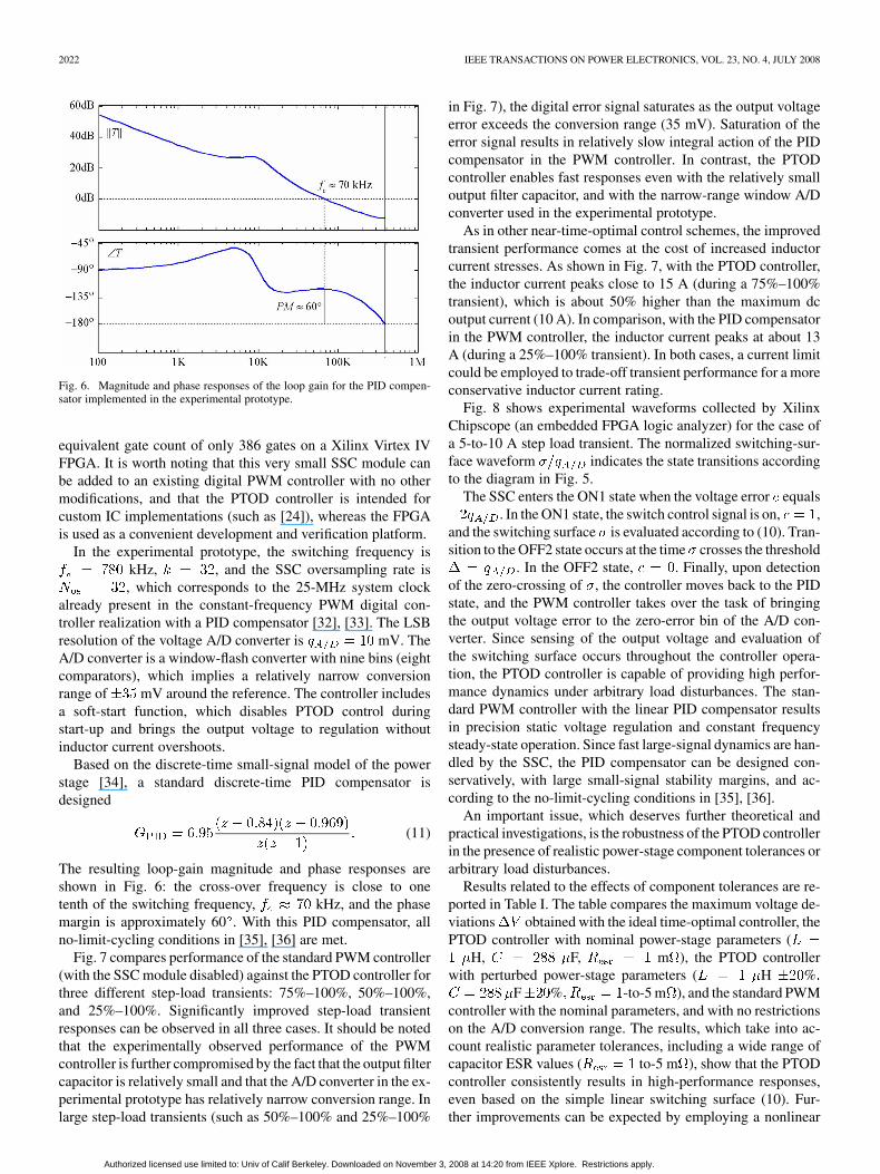
Fig. 6. Magnitude and phase responses of the loop gain for the PID compen-sator implemented in the experimental prototype.
equivalent gate count of only 386 gates on a Xilinx Virtex IVFPGA. It is worth noting that this very small SSC module canbe added to an existing digital PWM controller with no othermodifications, and that the PTOD controller is intended forcustom IC implementations (such as [24]), whereas the FPGAis used as a convenient development and verification platform.
In the experimental prototype, the switching frequency iskHz, , and the SSC oversampling rate is, which corresponds to the 25-MHz system clock
already present in the constant-frequency PWM digital con-troller realization with a PID compensator [32], [33]. The LSBresolution of the voltage A/D converter is mV. TheA/D converter is a window-flash converter with nine bins (eightcomparators), which implies a relatively narrow conversionrange of mV around the reference. The controller includesa soft-start function, which disables PTOD control duringstart-up and brings the output voltage to regulation withoutinductor current overshoots.
Based on the discrete-time small-signal model of the powerstage [34], a standard discrete-time PID compensator isdesigned
(11)
The resulting loop-gain magnitude and phase responses areshown in Fig. 6: the cross-over frequency is close to onetenth of the switching frequency, kHz, and the phasemargin is approximately 60 . With this PID compensator, allno-limit-cycling conditions in [35], [36] are met.
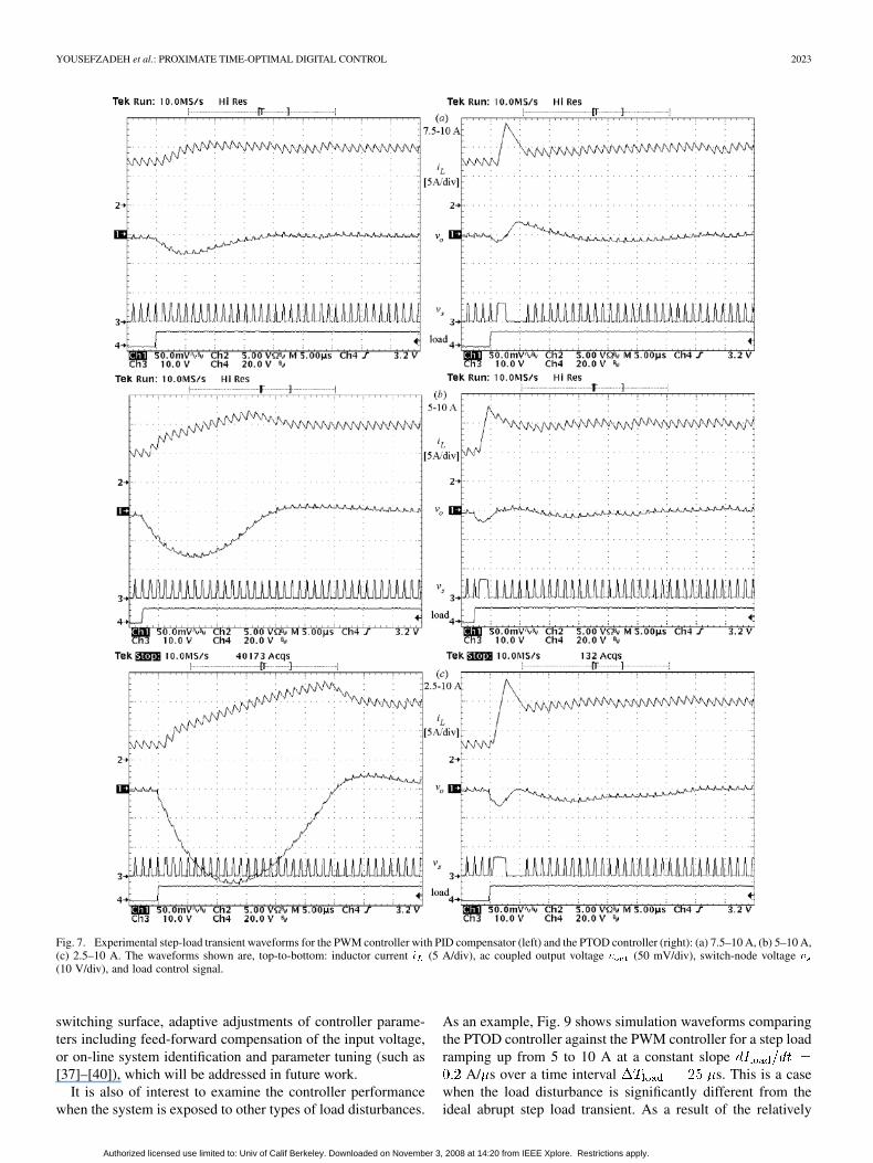
Fig. 7 compares performance of the standard PWM controller(with the SSC module disabled) against the PTOD controller forthree different step-load transients: 75%–100%, 50%–100%,and 25%–100%. Significantly improved step-load transientresponses can be observed in all three cases. It should be notedthat the experimentally observed performance of the PWMcontroller is further compromised by the fact that the output filtercapacitor is relatively small and that the A/D converter in the ex-perimental prototype has relatively narrow conversion range. Inlarge step-load transients (such as 50%–100% and 25%–100%
in Fig. 7), the digital error signal saturates as the output voltageerror exceeds the conversion range (35 mV). Saturation of theerror signal results in relatively slow integral action of the PIDcompensator in the PWM controller. In contrast, the PTODcontroller enables fast responses even with the relatively smalloutput filter capacitor, and with the narrow-range window A/Dconverter used in the experimental prototype.
As in other near-time-optimal control schemes, the improvedtransient performance comes at the cost of increased inductorcurrent stresses. As shown in Fig. 7, with the PTOD controller,the inductor current peaks close to 15 A (during a 75%–100%transient), which is about 50% higher than the maximum dcoutput current (10 A). In comparison, with the PID compensatorin the PWM controller, the inductor current peaks at about 13A (during a 25%–100% transient). In both cases, a current limitcould be employed to trade-off transient performance for a moreconservative inductor current rating.
Fig. 8 shows experimental waveforms collected by XilinxChipscope (an embedded FPGA logic analyzer) for the case ofa 5-to-10 A step load transient. The normalized switching-sur-face waveform indicates the state transitions accordingto the diagram in Fig. 5.
The SSC enters the ON1 state when the voltage error equals. In the ON1 state, the switch control signal is on, ,
and the switching surface is evaluated according to (10). Tran-sition to the OFF2 state occurs at the time crosses the threshold
. In the OFF2 state, . Finally, upon detectionof the zero-crossing of , the controller moves back to the PIDstate, and the PWM controller takes over the task of bringingthe output voltage error to the zero-error bin of the A/D con-verter. Since sensing of the output voltage and evaluation ofthe switching surface occurs throughout the controller opera-tion, the PTOD controller is capable of providing high perfor-mance dynamics under arbitrary load disturbances. The stan-dard PWM controller with the linear PID compensator resultsin precision static voltage regulation and constant frequencysteady-state operation. Since fast large-signal dynamics are han-dled by the SSC, the PID compensator can be designed con-servatively, with large small-signal stability margins, and ac-cording to the no-limit-cycling conditions in [35], [36].
An important issue, which deserves further theoretical andpractical investigations, is the robustness of the PTOD controllerin the presence of realistic power-stage component tolerances orarbitrary load disturbances.
Results related to the effects of component tolerances are re-ported in Table I. The table compares the maximum voltage de-viations obtained with the ideal time-optimal controller, thePTOD controller with nominal power-stage parameters (
H, F, m ), the PTOD controllerwith perturbed power-stage parameters ( H %
F % -to-5 m ), and the standard PWMcontroller with the nominal parameters, and with no restrictionson the A/D conversion range. The results, which take into ac-count realistic parameter tolerances, including a wide range ofcapacitor ESR values ( to-5 m ), show that the PTODcontroller consistently results in high-performance responses,even based on the simple linear switching surface (10). Fur-ther improvements can be expected by employing a nonlinear
Authorized licensed use limited to: Univ of Calif Berkeley. Downloaded on November 3, 2008 at 14:20 from IEEE Xplore. Restrictions apply.
YOUSEFZADEH et al.: PROXIMATE TIME-OPTIMAL DIGITAL CONTROL 2023
Fig. 7. Experimental step-load transient waveforms for the PWM controller with PID compensator (left) and the PTOD controller (right): (a) 7.5–10 A, (b) 5–10 A,(c) 2.5–10 A. The waveforms shown are, top-to-bottom: inductor current i (5 A/div), ac coupled output voltage v (50 mV/div), switch-node voltage v
(10 V/div), and load control signal.
switching surface, adaptive adjustments of controller parame-ters including feed-forward compensation of the input voltage,or on-line system identification and parameter tuning (such as[37]–[40]), which will be addressed in future work.
It is also of interest to examine the controller performancewhen the system is exposed to other types of load disturbances.
As an example, Fig. 9 shows simulation waveforms comparingthe PTOD controller against the PWM controller for a step loadramping up from 5 to 10 A at a constant slope
A/ s over a time interval s. This is a casewhen the load disturbance is significantly different from theideal abrupt step load transient. As a result of the relatively
Authorized licensed use limited to: Univ of Calif Berkeley. Downloaded on November 3, 2008 at 14:20 from IEEE Xplore. Restrictions apply.

2024 IEEE TRANSACTIONS ON POWER ELECTRONICS, VOL. 23, NO. 4, JULY 2008
Fig. 8. Experimental logic analyzer (Chipscope) waveforms collected from theFPGA controller prototype for the PTOD controller during a 5-to-10 A step loadtransient.
TABLE IPEAK OUTPUT VOLTAGE DEVIATION �V WORST-CASE PTODRESULTS ARE REPORTED FOR L = 1 �H �20%; C = 288 �F
�20%;R = 1-TO-5 m
slow increase in load current, the conditions for switching fromPID to SSC in the PTOD controller are met after a consider-able delay. Furthermore, the on/off switching action of the SSCis clearly not optimal. Nevertheless, the PTOD controller stillresults in smaller output voltage deviation compared tothe standard PWM controller where the SSC controller is dis-abled. Switching back to constant-frequency PWM operation isaccomplished without further disturbances in the output voltage.
The test has been repeated for various load slopes ,i.e., for various values of the time . The results are shownin Fig. 10, comparing the maximum voltage deviationsobtained with the PTOD controller against the values obtainedby the standard PWM controller, with no restrictions on the A/Dconversion range. With the PTOD controller, is alwaysless than 30 mV. For fast step-load transients, this is consid-erably better than with the standard PWM controller. For veryslow load transients, i.e., for s, or
A/ s, the conditions for switching to SSC are never met,and the PTOD performs exactly the same as the PWM controllerwith PID compensator. The results of Fig. 10 illustrate advan-tages of the architecture that combines capabilities for fast ac-tion based on a switching-surface control law, with robustness
Fig. 9. Transient responses with the PTOD controller (blue) and with the PWMcontroller (red) when the load current increases at a slope of dI =dt =
0:2 A/�s.
Fig. 10. Peak output voltage deviation �V with the PTOD controller andwith the PWM controller as functions of the step-load increase time �T .The switching surface controller (SSC) portion of the PTOD controller is acti-vated for step-load transients faster than approximately 0.17 A/�s.
and steady-state performance of a standard constant-frequencyPWM controller.
VI. CONCLUSION
This paper introduces an approach to near time-optimal con-trol in synchronous buck dc–dc converters using a simple digitalcontroller realization. The proposed PTOD controller is a com-bination of a constant-frequency PWM controller employinglinear PID compensator close to a reference point, and a linear or
Authorized licensed use limited to: Univ of Calif Berkeley. Downloaded on November 3, 2008 at 14:20 from IEEE Xplore. Restrictions apply.

YOUSEFZADEH et al.: PROXIMATE TIME-OPTIMAL DIGITAL CONTROL 2025
nonlinear SSC away from the reference, together with a smoothtransition between the two modes. A key component of the SSCis a hybrid capacitor current estimator that enables effectiveswitching surface evaluation even with a relatively low-resolu-tion hardware, and eliminates the need for current sensing. TheSSC, which is implemented as a Verilog HDL module, is verysimple and small (less than 400 gates). The SSC module canbe easily added to an existing digital controller to construct thePTOD controller. In steady state, the controller operates exactlythe same as a standard constant-frequency PWM controller witha linear PID compensator. Simulation and experimental resultsare shown for a 6.5–1.3 V, 10 A synchronous buck converter.
REFERENCES
[1] R. D. Middlebrook and S. Cuk, “A general unified approach to mod-eling switching-converter power stages,” Int. J. Electron., vol. 42, no.6, pp. 521–550, Jun. 1977.
[2] R. W. Erickson and D. Maksimovic, Fundamentals of Power Elec-tronics. New York: Springer, 2000.
[3] W. Burns and T. Wilson, “Analytic derivation and evaluation of a state-trajectory control law for dc–dc converters,” Proc. IEEE PESC, pp.70–85, 1977.
[4] P. T. Krein, Elements of Power Electronics. Oxford, U.K.: OxfordUniv. Press, 1998.
[5] B. Jammes, J. C. Marpinard, and L. Martinez-Salamero, “Large-signalcontrol of a buck converter based on time optimal control,” in Proc.ECCTD, 1993, pp. 1419–1422.
[6] D. Biel, L. Martinez, J. Tenor, B. James, and J. C. Marpinard, “Op-timum dynamic performance of a buck converter,” in Proc. IEEEISCAS, 1996, vol. 1, pp. 589–592.
[7] A. Capel and D. O’Sullivan, “Very high frequency regulator for spaceapplications,” in Proc. IEEE PESC, 1996, vol. 1, pp. 846–852.
[8] P. Gupta and A. Patra, “Super-stable energy based switching controlscheme for dc–dc buck converter circuits,” in Proc. IEEE ISCAS, 2005,vol. 4, pp. 3063–3066.
[9] K. K. S. Leung and H. S. H. Chung, “Derivation of a second-orderswitching surface in the boundary control of buck converters,” IEEEPower Electron. Lett., vol. 20, no. 2, pp. 63–67, Jun. 2004.
[10] K. S. Leung and H. S. H. Chung, “A comparative study of the boundarycontrol of buck converters using first- and second-order switchingsurfaces -Part I: Continuous conduction mode,” in Proc. IEEE PESC,2005, pp. 2133–2139.
[11] K. S. Leung and H. S. H. Chung, “A comparative study of the boundarycontrol of buck converters using first- and second-order switching sur-faces–Part II: Discontinuous conduction mode,” in Proc. IEEE PESC,2005, pp. 2126–2132.
[12] M. Ordonez, M. T. Iqbal, and J. E. Quaicoe, “Selection of a curvedswitching surface for buck converters,” IEEE Trans. Power Electron.,vol. 21, no. 4, pp. 1148–1153, Jul. 2006.
[13] J. T. Mossoba and P. T. Krein, “Exploration of deadbeat control fordc–dc converters as hybrid systems,” in Proc. IEEE PESC, Jun. 2005,pp. 1004–1010.
[14] G. E. Pitel and P. T. Krein, “Trajectory paths for dc–dc converters andlimits to performance,” in Proc. IEEE COMPEL, 2006, pp. 40–47.
[15] P. T. Krein, “Feasibility of geometric digital controls and augmentationfor ultrafast dc–dc converter response,” in Proc. IEEE COMPEL, 2006,pp. 48–56.
[16] M. Athans and P. Falb, Optimal Control: An Introduction to The Theoryand Its Applications. New York: McGraw-Hill, 1966.
[17] A. S. I. Zinober and A. T. Fuller, “The sensitivity of nominally time-optimal control systems to parameter variation,” Int. J. Contr., vol. 17,no. 4, pp. 673–703, 1973.
[18] W. S. Newman, “Robust near time-optimal control,” IEEE Trans. Au-tomat. Contr., vol. 35, no. 7, pp. 841–844, Jul. 1990.
[19] L. Y. Pao and G. F. Franklin, “Proximate time-optimal control of third-order servomechanisms,” IEEE Trans. Automat. Contr., vol. 38, no. 4,pp. 560–580, Apr. 1993.
[20] L. Y. Pao and G. F. Franklin, “The robustness of a proximate time-optimal controller,” IEEE Trans. Automat. Contr., vol. 39, no. 9, pp.1963–1966, Sep. 1994.
[21] C. Laorpacharapan and L. Y. Pao, “Shaped time-optimal feedback con-trol for disk-drive systems with back-electromotive force,” IEEE Trans.Magn., vol. 40, no. 1, pp. 85–96, Jan. 2004.
[22] E. Alarcón, D. Biel, F. Guinjoan, E. Fossas, E. Vidal, and A. Poveda,“Current-mode BiCMOS sliding-mode controller circuit for AC signalgeneration in switching power dc–dc converters,” in Proc. IEEEMWSCAS99, Aug. 1999.
[23] S. Gomáriz, E. Alarcón, J. A. Martínez, A. Poveda, J. Madrenas, andF. Guinjoan, “Minimum-time control of a buck converter by meansof fuzzy logic approximation,” in Proc. IEEE IECON’98, 1998, pp.1060–1065.
[24] B. Patella, A. Prodic, A. Zirger, and D. Maksimovic, “High-frequencydigital PWM controller IC for dc–dc converters,” IEEE Trans. PowerElectron., vol. 18, no. 1, pp. 438–446, Jan. 2003.
[25] D. Maksimovic, R. Zane, and R. Erickson, “Impact of digital controlin power electronics,” in Proc. IEEE Int. Symp. Power SemiconductorDevices ICs, 2004, pp. 13–22.
[26] G. Feng, E. Meyer, and Y. F. Liu, “A new digital control algorithm toachieve optimal dynamic performance in dc-to-dc converters,” IEEETrans. Power Electron., vol. 22, no. 4, pp. 1489–1498, Jul. 2007.
[27] G. Feng, E. Meyer, and Y. F. Liu, “High performance digital controlalgorithms for dc–dc converters based on the principle of capacitorcharge balance,” in Proc. IEEE PESC, 2006, pp. 1–7.
[28] E. Meyer, G. Feng, and Y. F. Liu, “Novel digital controller improvesdynamic response and simplifies design process of voltage regulatormodule,” in Proc. IEEE APEC, 2007, pp. 1447–1453.
[29] J. Quintero, A. Barrado, M. Sanz, A. Lazaro, and E. Olias, “Experi-mental validation of the advantages provided by linear-non-linear con-trol in multi-phase VRM,” in Proc. IEEE APEC, 2007, pp. 707–713.
[30] A. Soto, P. Alou, and J. A. Cobos, “Nonlinear digital control breaksbandwidth limitations,” in Proc. IEEE APEC, 2006.
[31] Z. Zhao and A. Prodic, “Continuous-time digital controller for high-frequency dc–dc converters,” IEEE Trans. Power Electron., vol. 23, no.2, pp. 564–573, Mar. 2008.
[32] H. Hu, V. Yousefzadeh, and D. Maksimovic, “Nonlinear control forimproved dynamic response of digitally-controlled dc–dc converters,”in Proc. IEEE PESC, 2006, pp. 1–7.
[33] V. Yousefzadeh, T. Takayama, and D. Maksimovic, “Hybrid DPWMwith digital delay-locked loop,” in Proc. IEEE COMPEL, 2006, pp.142–148.
[34] D. M. Van de Sype, K. De Gusseme, F. M. L. L. De Belie, A. P. Vanden Bossche, and J. A. Melkebeek, “Small-signal z-domain analysis ofdigitally controlled converters,” IEEE Trans. Power Electron., vol. 21,no. 2, pp. 470–478, Mar. 2006.
[35] A. V. Peterchev and S. R. Sanders, “Quantization resolution and limitcycling in digitally controlled PWM converters,” IEEE Trans. PowerElectron., vol. 18, no. 1, pp. 301–308, Jan. 2003.
[36] H. Peng, A. Prodic, E. Alarcon, and D. Maksimovic, “Modeling ofquantization effects in digitally controlled dc–dc converters,” IEEETrans. Power Electron., vol. 22, no. 1, pp. 208–215, Jan. 2007.
[37] B. Miao, R. Zane, and D. Maksimovic, “System identification of powerconverters with digital control through cross-correlation methods,”IEEE Trans. Power Electron., vol. 20, no. 5, pp. 1093–1099, Sep.2005.
[38] W. Stefanutti, P. Mattavelli, S. Saggini, and M. Ghioni, “Autotuning ofdigitally controlled dc–dc converters based on relay feedback,” IEEETrans. Power Electron., vol. 22, no. 1, pp. 199–207, Jan. 2007.
[39] S. Saggini, W. Stefanutti, E. Tedeschi, and P. Mattavelli, “Digital dead-beat control tuning for dc–dc converters using error correlation,” IEEETrans. Power Electron., vol. 22, no. 4, pp. 1566–1570, Jul. 2007.
[40] W. Stefanutti, E. Della Monica, E. Tedeschi, P. Mattavelli, and S. Sag-gini, “Reduction of quantization effects in digitally controlled dc–dcconverters using inductor current estimation,” in Proc. IEEE PESC,2006, pp. 1–7.
Vahid Yousefzadeh (S’03–M’06) received the B.S.degree in electrical engineering from AmirkabirUniversity of Technology, Tehran, Iran, in 1994,and the M.S. and Ph.D. degrees from the ColoradoPower Electronics Center (CoPEC), University ofColorado, Boulder, in 2004 and 2006, respectively.
From June to December 2006, he was a CoPECPostdoctoral Researcher. Since 2007, he has beenwith the Digital Power Group of Texas Instruments,Dallas, TX, where he is currently a System DesignEngineer. His research interests include digital
control techniques, switch-mode power supply (SMPS) modeling, and control.
Authorized licensed use limited to: Univ of Calif Berkeley. Downloaded on November 3, 2008 at 14:20 from IEEE Xplore. Restrictions apply.

2026 IEEE TRANSACTIONS ON POWER ELECTRONICS, VOL. 23, NO. 4, JULY 2008
Amir Babazadeh (S’03) received the B.S. degree inelectrical engineering from Amirkabir University ofTechnology (Tehran Polytechnic), Tehran, Iran, andthe M.S. degree in systems and control from SharifUniversity of Technology, Tehran, in 2000 and 2002,respectively. He is currently pursuing the Ph.D. de-gree at the University of Colorado at Boulder.
From 2003 to 2006, he was performing researchunder a ZF (Central Research Supporting Organiza-tion for Young Researchers) scholarship at the Uni-versity of Bremen, Bremen, Germany. His current re-
search interests include optimal control, piecewise linear systems, digital con-trol, and power electronics.
Bhaskar Ramachandran received the B.E. degreein electrical engineering from the College of Engi-neering Guindy, Anna University, in 2002 and theM.S degree in electrical engineering from the Uni-versity of Colorado at Boulder in 2007.
From 2002 to 2005, he was with Texas InstrumentsIndia Pvt. Ltd., designing analog power managementcircuits. Since September 2007, he has been with Na-tional Semiconductor, where he is currently a SeniorDesign Engineer working on portable power manage-ment circuit designs. His research interests include
analog, mixed signal, and digital power management circuit design for portablesystems.
Eduard Alarcón (S’96–M’01) received the M.S.(national award) and Ph.D. degrees in electricalengineering from the Technical University ofCatalunya (UPC), Barcelona, Spain, in 1995 and2000, respectively.
Since 1995, he has been with the Department ofElectronic Engineering at the Technical University ofCatalunya, where he became an Associate Professorin 2000. Since 2006, he has been Vice Dean of In-ternational Affairs at the School of Electrical Engi-neering, UPC. From August 2003 to January 2004,
and in the summer of 2006, he was a Visiting Professor at the CoPEC center,University of Colorado at Boulder. He has co-authored more than 100 inter-national scientific publications, three book chapters, and two patents, and hasbeen involved in different national and U.S. R&D projects. His current researchinterests include the areas of analog and mixed-signal integrated circuits andon-chip power management circuits. He has given nine invited plenary lecturesor tutorials in Europe, the U.S., and Asia.
Dr. Alarcón received the Myril B. Reed Best Paper Award at the 1998 IEEEMidwest Symposium on Circuits and Systems. He was the invited co-editor of aspecial issue of the Analog Integrated Circuits and Signal Processing journal de-voted to current-mode circuit techniques. He co-organized two special sessionsrelated to on-chip power management at IEEE ISCAS03 (Bangkok, Thailand)and IEEE ISCAS06 (Kobe, Japan). He was the 2007 Chair of the IEEE Cir-cuits and Systems Society Technical Committee of Power Systems and PowerElectronics Circuits. He was the Technical Program Co-Chair of the 2007 Eu-ropean Conference on Circuit Theory and Design—ECCTD07 (Seville, Spain),Track Chair of the IEEE ISCAS 2007 (New Orleans, LA) and IEEE ISCAS 2008(Seattle, WA) and IEEE MWSCAS07 (Montreal, QC, Canada). He served as anAssociate Editor of the IEEE TRANSACTIONS ON CIRCUITS AND SYS-TEMS—I (2006–2007) and for the IEEE TRANSACTIONS ON CIRCUITSAND SYSTEMS—II (2006–2007). He is currently an Associate Editor of theIEEE TRANSACTIONS CIRCUITS AND SYSTEMS—PART I.
Lucy Y. Pao (S’89–M’92–SM’98) received the B.S.,M.S., and Ph.D. degrees in electrical engineeringfrom Stanford University, Stanford, CA.
She is currently a Professor in the Electrical andComputer Engineering Department at the Universityof Colorado at Boulder. She has interests in the areasof control systems (with applications to flexiblestructures, disk drives, atomic force microscopes,wind turbines, tape systems, and power converters),multisensor data fusion (with applications to un-manned autonomous vehicles, military surveillance,
and satellite tracking), and haptic and multimodal visual/haptic/audio interfaces(with applications to scientific visualization and spatial communication).
Dr. Pao has received a number of awards and has been active in many profes-sional society committees and positions. Selected recent awards include a 2003Subaru Teaching Excellence Award, the Best Commercial Potential Award atthe 2004 International Symposium on Haptic Interfaces for Virtual Environ-ments and Teleoperator Systems, and the Best Paper Award at the 2005 WorldHaptics Conference. She was also a plenary speaker at the 2006 IEEE Confer-ence on Decision and Control. Selected recent and current professional societyactivities include serving as Program Chair for the 2004 American Control Con-ference (ACC), an elected member of the IEEE Control Systems Society Boardof Governors for 2005–2007, and a member of the 2006–2008 InternationalFederation of Automatic Control (IFAC) Congress Young Author Prize Selec-tion Committee. She is also on the Organizing Committee for the 2010 IFACSymposium on Mechatronic Systems, and will be General Chair for the 2013ACC.
Dragan Maksimovic (SM’05) received the B.S. andM.S. degrees in electrical engineering from the Uni-versity of Belgrade, Belgrade, Yugoslavia, in 1984and 1986, respectively, and the Ph.D. degree fromthe California Institute of Technology, Pasadena, in1989.
From 1989 to 1992, he was with the University ofBelgrade. Since 1992, he has been with the Depart-ment of Electrical and Computer Engineering, Uni-versity of Colorado at Boulder, where he is currentlya Professor and Director of the Colorado Power Elec-
tronics Center (CoPEC). His current research interests include digital controltechniques and mixed-signal integrated circuit design for power electronics.
Dr. Maksimovic received the National Science Foundation CAREER Awardin 1997, the Power Electronics Society Transactions Prize Paper Award in 1997,the Bruce Holland Excellence in Teaching Award in 2004, and the Universityof Colorado Inventor of the Year Award in 2006.
Authorized licensed use limited to: Univ of Calif Berkeley. Downloaded on November 3, 2008 at 14:20 from IEEE Xplore. Restrictions apply.
Related Documents