VLSI Design 6332 Proposal A Method to Implement Low Energy Read Operations, and Single Cycle Write After Read in Subthreshold SRAMs by The Sub-threshold Team Author Arijit Banerjee 11/8/2012

Welcome message from author
This document is posted to help you gain knowledge. Please leave a comment to let me know what you think about it! Share it to your friends and learn new things together.
Transcript

VLSI Design 6332
ProposalA Method to Implement Low Energy Read Operations, and
Single Cycle Write After Read in Subthreshold SRAMs
by
The Sub-threshold TeamAuthor
Arijit Banerjee
11/8/2012

TABLE OF CONTENTS
Chapter 1 Design Component, Research Component and Simulations for the Project ________________________________________________________________________2-3
Chapter 2 Proof of the Concept Simulation Figures and Corresponding Schematics______________________________________________________________________4-15
Chapter 3 Timeline for Project Completion and Intermediate Milestones _________________________________________________________________________16
Chapter 4 Results _______________________________________________________________17
Chapter 5 Remaining Task breakdown for group members ____________18
Chapter 6 References___________________________________________________________19
Page | 1

Chapter 1
Design Component, Research Component and Simulations for the Project
Findings from the prior works:
In [1], from the Fig. 8 (a) of the [1] shows that the Monte Carlo (MC) data indicating “mean-3sigma” RSNM of ST is lying in between 50mV to 0mV and “mean – 3sigma” hold signal to noise margin (HSNM) lying nearby 100mV. On the other hand in Fig. 9 the “mean + 3sigma” Vmin looks like lying in between 350-400mV. Hence, from the process variation and robustness standpoint with 400mV of supply voltage the 3sigma worse case values indicate that there may be failures in the bitcell in below 350mV if fabricated.
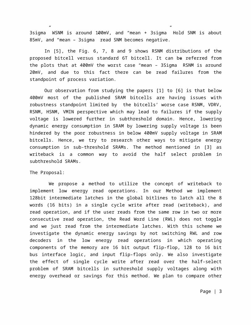
In [2], from the Fig. 7 it can be seen that the 3sigma worst case Read and Hold SNM is not robust at all. With 300 mV supply the “mean – 3sigma” WSNM is around 100mV, and “mean + 3sigma” Hold SNM is about 85mV, and “mean – 3sigma” read SNM becomes negative.
In [5], the Fig. 6, 7, 8 and 9 shows RSNM distributions of the proposed bitcell versus standard 6T bitcell. It can be referred from the plots that at 400mV the worst case “mean – 3Sigma” RSNM is around 20mV, and due to this fact there can be read failures from the standpoint of process variation.
Our observation from studying the papers [1] to [6] is that below 400mV most of the published SRAM bitcells are having issues with robustness standpoint limited by the bitcells’ worse case RSNM, VDRV, RSNM, HSNM, VMIN perspective which may lead to failures if the supply voltage is lowered further in subthreshold domain. Hence, lowering dynamic energy consumption in SRAM by lowering supply voltage is been hindered by the poor robustness in below 400mV supply voltage in SRAM bitcells. Hence, we try to research other ways to mitigate energy consumption in sub-threshold SRAMs. The method mentioned in [3] as writeback is a common way to avoid the half select problem in subthreshold SRAMs.
The Proposal:
We propose a method to utilize the concept of writeback to implement low energy read operations. In our Method we implement 128bit intermediate latches in the global bitlines to latch all the 8 words (16 bits) in a single cycle write after read (writeback), and read operation, and if the user reads from the same row in two or more consecutive read operation, the Read Word Line (RWL) does not toggle and we just read from the intermediate latches. With this scheme we investigate the dynamic energy savings by not switching RWL and row decoders in the low energy read operations in which operating components of the memory are 16 bit output flip-flop, 128 to 16 bit bus interface logic, and input flip-flops only. We also investigate the effect of single cycle write after read over the half-select problem of SRAM bitcells in suthreshold supply voltages along with energy overhead or savings for this method. We plan to compare other methods for SRAM dynamic energy reduction with the proposed one in the next design review.
Page | 2
Motivation:
There was a version of sub-threshold data memory without column mux used in UVa Body Sensor Network (BSN) chip last year 2011. The memory had normal 128 bits of DIN and DOUTs directly providing to the user with operating voltage of 0.5 volt and frequency of 200 kHz. In the memory the writing operation was done in effective two cycles by write after read approach which is standard in sub-threshold memories to avoid the half select issue. Recently the BSN chip team has changed the BSN Instruction Set Architecture (ISA) along with the bus width of the main data and address bus to 16 bit each, and they demanded new features in the memory like somehow single cycle effectively writing, lowering the read dynamic power dissipation, and other features like including input and output flops, converting the existing 128bit bus to 16 bit bus interface to the SOC, and so on. In order to meet their requirements we added new circuits and modified the Data memory to meet the specification.
Design component, research component and simulations for the projects:
We tabulated the regular design components, research components and simulations to be done for the project as follows:
Regular Design Component Research Component
i) Low Energy Read
ii)
iii)
iv)
Simulations to be done for The Project
128bit to 16bit bus interface logic
Normal Read , and Single Cycle Write After Read for functionality
Pulse generator and Single Cycle Write after Read Control logic
Single Cycle Write After Read
Low Energy Read and Normal Read simulations for energy comparison for
0.5v, 0.4v, 0.3v and one superthreshold voltage 0.9v for energy
trend comparison
Comparator/Statemachine for Low Energy Support
Each individual New Components' Functionality Check
Intermediate Latches for Low Energy Read and Single Cycle
Write after Read
Chapter 2 Page | 3

Proof of the Concept Simulation Figures and Corresponding Schematics
For the proof of concept we provide the suggested pin description table, and timing diagrams, taken from “SRAM Specification Document November Test Chip 2012.doc” from BSN chip team followed by actual schematic and simulation figures, from the next page. Rest of this page is intentionally left blank for formatting. The pins correspond to the low Energy Read operations of the memory in the pin description table are BURSTENB and BURST_RESET and the mode is called “BURST” in the SRAM Memory Specification Document.
Pin Description Table for the DATA Memory:
Page | 4
Pin Name Pin Description
Input Pins
CLK
DIN<0:15> PE
ADR<0:10> PE
ENABLEB PE
READWB PE
EN<0:3> PE
WR<0:2> PE
BURSTENB PE
BURST_RESET asynch
Latching Edge
All the input pins are having their own flops in the memories and they are latched in the pos-edge of the external clock (expeption- BURST_RESET is
asych)CLK is the external clock pin which controls the SRAM. Input data is
latched on the rising edge of the clock, output data is latched on the falling edge of the clock
DIN stands for data input bus pins, and should be asserted 1 or 0 before the clk positive edge accordingly, given a setup time is provided.
ADR stands for address bus pins. Should be asserted 1 or 0 before the clk positive edge accordingly, given a setup time is provided.
ENABLEB is a active low clock gating pin for the SRAM. In case of asserted to 0, it allows the SRAM to operate else it gates the clock and stops all read or write operation, but the internal content of the memory remains valid.
READWB is the pin for selecting an read or write operation. If asserted 1, it allows the read operation. In case of asserting the same to 0, it allows
write operation.
EN is an active low power gating pin for each of the SRAM banks. 4KB memories will have 4 banks (EN<0:3>), 2KB memories will have 2 banks
(EN<0:1>). If no banks are active, then the periphery is automatically power gated.
WR stands for write after read delay control pin, and should be asserted a proper 3 bit value before the positive edge of the clock accordingly, given
a setup time is provided.
BURSTENB is an active low pin, allowing for burst enable read operations. Setting this pin high will disable burst mode reads, allowing us to compare
the energy savings of using burst enable
BURST_RESET is an asychronus reset pin, which will be responsible for resetting the burst enable register. This will ensure that the first read operation after power up does not use the burst enable mode. This signal will be controlled by the global reset signal
Output Pins
DOUT<0:15> NEDOUT stands for data output bus pins. The data is latched on the negative
edge of the clock and remains valid until the next negative clock edge.
Timing Diagrams for Read Operation: The timing diagram provided represents two consecutive read operations and a write operation. Other internal signals like internal clock,
Page | 5
TaccTsuTsu
Tcyc
T_Clk2DIN Internal
internally latched DIN and ADR signal, and read word line (RWL) and write word line (WWL) are also specified for clarity.
Timing Diagrams for Write after Read Operation: The timing diagram provided below represents two consecutive write after read operations and a read operation. Signals like
Page | 6

CLK
ENABLEB
ADR
DOUT
DIN
READWB
Tacc
Tsu
TsuTsu
Tsu
Th
Th
Tcyc
Th
Last State
Internally Latched ADR
T_Clk2ADR Internal
Internally Latched DIN
T_Clk2DIN Internal
Internal RWL
Internal WWL
RWL Pulse-width
WWL Pulse-width
Internal CLK
internal clock, read word line (RWL) and write word line (WWL) are also specified. In the write after read operation the output bus retains the last state.
Internal Change of Waveforms for WR value change:
Page | 7

CLK
Tcyc
WRTsu Th
T_Clk2WR Internal
Mode 00 Mode 01, 10, etc. > 00
READWB ThTsu
RWL
WWL
RWL Pulse-width
WWL Pulse-width
Increased RWL Pulse-width
Decreased WWL Pulse-width
Internally Latched WR
Internal CLK
Annotated full schematic of 4KB subthreshold SRAM data memory:
Page | 8

Fig. 1-a
Simulated and annotated waveform of the single cycle write after read, and normal read operations:
Page | 9
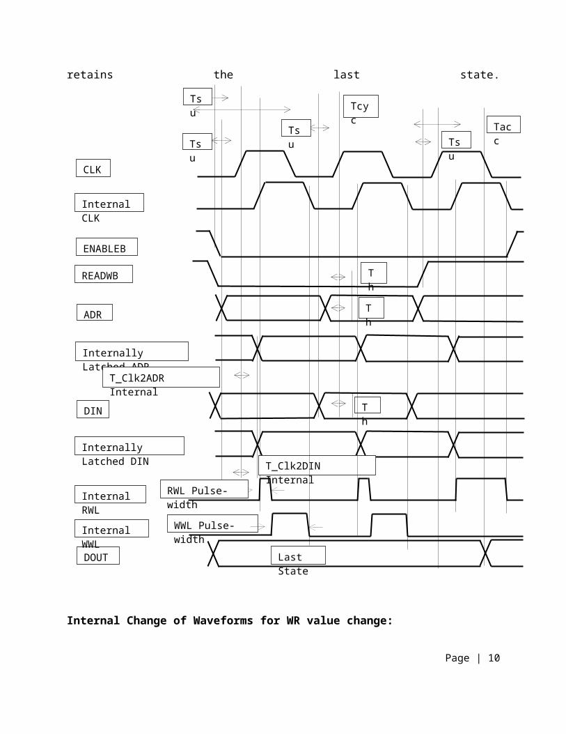
Fig. 1-b
Simulated and annotated waveform of the low energy read operations:Page | 10

Fig. 1-c
Simulated and annotated waveform of the low energy read operations for energy measurement:
Page | 11

Fig. 1-d
Annotated schematic for low energy read operation support in 4KB subthreshold SRAM data memory :Page | 12

Fig. 2
Page | 13

Annotated schematic for single cycle write after read control logic, output-flop, and 128 bit intermediate latch clock generation logic in 4KB subthreshold SRAM data memory:
Fig. 3
Page | 14

16 bit bus controller and 128-to-16bit bus interface logic:
Fig. 4
Page | 15

Chapter 3
Timeline for Project Completion and Intermediate Milestones
Timeline and Milestone:
We already build these above sub-circuitry for low energy read operation support, single cycle write after read, 128 to 16 bit bus multiplexers, intermediate 128 bit latches and input and output flops. As this memory will always be operated at room temperature, we are simulating the same in 27C temperature only. We have simulated our sub-threshold memory in some PVTs including the PVT of TT_0.5V_27C corner and the functionality we are getting from simulation is what we intended. The supply voltage of 0.5V was chosen by the BSN chip group as the supply for the digital logic used is 0.5v. The memory is already been working with the supply voltage near by the “mean +3 sigma” DRV Vmin of the bitcell which is nearly 350mV. The timeline table provided for this project is as follows:
Timeline:
Tasks Completion Deadline Status1) Schematic Implementation of Low Energy Read 9/7/2012 Done
2) Schematic Implementation of Single Cycle Write after Read 9/14/2012 Done
3) 10/10/2012 Done
4) 10/10/2012 Done5) Building Layouts of each new component block 10/10/2012 Done6) Integrating Layouts to Data Memory 10/30/2012 Done7) Running DRC and LVS 10/30/2012 Done8) Sign off and Tape out on November 7th 2012 11/7/2012 Done9) Extracting Lumped parasitics 11/14/2012 To Do10) Simulate in TT, SS, FF corner with lumped parasitics 11/14/2012 To Do
11) 11/14/2012 To Do
12) 11/23/2012 To Do
Measuring the Energy Saving in Low Energy Mode for in TT, FF, SS, SF and FS corners with 0.5v supply voltage
Checking Design Margins in TT, FF, SS, SF and FS corner with 0.5V supply and 27C temperature for at least one WR mode
Low Energy Read and Normal Read simulations, Single cycle Write After Read Simulations for energy comparison for 0.5v, 0.4v, 0.3v and one superthreshold voltage 0.9v for energy trend comparison
HSIM vs. Spectre Simulation Comparison for Low Energy Read
Page | 16

Chapter 4
Results
We simulated the low energy read operations preceded by the normal read operations and got the following table for energy savings in Joules. We used HSIM with highest SPICE accuracy.
TT 1.54E-12 2.10E-13 7.35FF 1.88E-12 3.23E-13 5.82SS 1.44E-12 1.77E-13 8.12SF 1.27E-12 1.81E-13 7.02
Corners 27C 500mV
Worst Case Read Energy In Normal Read Mode in
Joules
Worst Case Energy Dissipation in Low Energy Read Mode in
Joules
Energy Savings in terms of multiplier
(X)
For the robustness of the Write After Read operation, we tabulated the read word line and write word line pulse widths in valid Read and Write After Read operations for all WR<0:3> modes with TT and FF process corners, and marked failures in failed cases of functionality for internal SRAM margin issues as follows:
Measured Parameters TT FFWR Mode RWL WWL 128 Bit Latch Tacc RWL WWL 128 Bit Latch Tacc
000 92.2n 2.34u 90.1n 2.41u failed failed failed failed001 227n 2.2u 225n 2.41u 27n 2.39u 26.2n 2.41u010 293n 2.14u 291n 2.41u 35.6n 2.39u 34.8n 2.41u011 368n 2.06u 366n 2.41u 43.6n 2.37u 42.8n 2.41u100 451n 1.98u 449n 2.41u 52.6n 2.36u 51.9n 2.41u101 514n 1.92u 512n 2.41u 60.8n 2.35u 60n 2.41u110 610n 1.82u 608n 2.41u 73.3n 2.34u 72.5n 2.41u111 721n 1.71u 719n 2.41u 85.1n 2.33u 84.3n 2.41u
Pulse Width Data for DMEM
From the measurement we can see that in WR mode “000” the Memory functionality is “failed” in FF corner due to insufficient margin to generate read word line and write word line pulses correctly. Sill there are plenty of modes in those the SRAM operates successfully. Some of the simulation results are yet to be populated in SS, SF, and FS corners in those modes.
Chapter 5 Page | 17

Remaining Task breakdown for group members
Below is the Timeline-table including the name of the owner of each task: Here two tasks are performed solely by a BSN chip group member named Jim (James Boley) and another shared task, and he is not a member of the VLSI 6332 “Subthreshold Group.”
Tasks Completion Deadline Status Owner1) Schematic Implementation of Low Energy Read 9/7/2012 Done Arijit
2) Schematic Implementation of Single Cycle Write after Read 9/14/2012 Done Arijit
3) 10/10/2012 Done Arijit
4) 10/10/2012 Done Arijit5) Building Layouts of each new component block 10/10/2012 Done Arijit6) Integrating Layouts to Data Memory 10/30/2012 Done Jim7) Running DRC and LVS 10/30/2012 Done Jim
8) Sign off and Tape out on November 7th 2012 11/7/2012 Done9) Extracting Lumped parasitics 11/14/2012 To Do Arijit10) Simulate in TT, SS, FF corner with lumped parasitics 11/14/2012 To Do Arijit
11) 11/14/2012 To Do Arijit
12) 11/23/2012 To Do Arijit
Measuring the Energy Saving in Low Energy Mode for in TT, FF, SS, SF and FS corners with 0.5v supply voltage
Checking Design Margins in TT, FF, SS, SF and FS for at least one WR mode
Arijit & Jim
Low Energy Read and Normal Read simulations, Single cycle Write After Read Simulations for energy comparison for 0.5v, 0.4v, 0.3v and one superthreshold voltage 0.9v for energy trend comparison
HSIM vs. Spectre Simulation Comparison for Low Energy Read
Chapter 6
Page | 18

References
[1] J. P. Kulkarni, K. Kim, and K. Roy, “A 160 mV Robust Schmitt Trigger Based Subthreshold SRAM,” IEEE Journal of Solid-State Circuits, vol. 42, no. 10, pp. 2303–2313, Oct. 2007.
[2] I. J. Chang, J.-J. Kim, S. P. Park, and K. Roy, “A 32 kb 10T Sub-Threshold SRAM Array With Bit-Interleaving and Differential Read Scheme in 90 nm CMOS,” IEEE Journal of Solid-State Circuits, vol. 44, no. 2, pp. 650–658, Feb. 2009.
[3] T. H. Kim, J. Liu, J. Keane, and C. H. Kim, “A high-density subthreshold SRAM with data-independent bitline leakage and virtual ground replica scheme,” in Solid-State Circuits Conference, 2007. ISSCC 2007. Digest of Technical Papers. IEEE International, 2007, pp. 330–606.
[4] B. H. Calhoun and A. Chandrakasan, “A 256kb sub-threshold SRAM in 65nm CMOS,” in Solid-State Circuits Conference, 2006. ISSCC 2006. Digest of Technical Papers. IEEE International, 2006, pp. 2592–2601.
[5] G. K. Reddy, K. Jainwal, J. Singh, and S. P. Mohanty, “Process variation tolerant 9T SRAM bitcell design,” in Quality Electronic Design (ISQED), 2012 13th International Symposium on, 2012, pp. 493–497.
[6] Ali Valaee, Asim J. Al-Khalili, “SRAM Read-Assist Scheme for High Performance Low Power Applications” in International SoC Design Conference (ISOCC), 2011, pp. 179-182.
Page | 19
Related Documents