Properties of aluminum oxide thin films deposited by pulsed laser deposition and plasma enhanced chemical vapor deposition C. Cibert ⁎ , H. Hidalgo, C. Champeaux, P. Tristant, C. Tixier, J. Desmaison, A. Catherinot SPCTS UMR-CNRS no. 6638, Faculté des Sciences et Techniques, 123 avenue A. Thomas, 87060 Limoges Cedex, France Received 9 August 2006; received in revised form 25 May 2007; accepted 30 May 2007 Available online 6 June 2007 Abstract The chemical, structural, mechanical and optical properties of thin aluminum oxide films deposited at room temperature (RT) and 800 °C on (100) Si and Si–SiO 2 substrates by pulsed laser deposition and plasma enhanced chemical vapor deposition are investigated and compared. All films are smooth and near stoichiometric aluminum oxide. RT films are amorphous, whereas γ type nano-crystallized structures are pointed out for films deposited at 800 °C. A dielectric constant of ∼ 9 is obtained for films deposited at room temperature and 11–13 for films deposited at 800 °C. Young modulus and hardness are in the range 116–254 GPa and 6.4–28.8 GPa respectively. In both cases, the results show that the deposited films have very interesting properties opening applications in mechanical, dielectric and optical fields. © 2007 Elsevier B.V. All rights reserved. Keywords: Aluminum oxide; PECVD; PLD; Thin films properties 1. Introduction According to their excellent mechanical, optical and electrical properties, aluminum oxide thin films are used in a very large range of applications, such as wear-resistant coatings [1], corrosion-resistant barriers [2], optical wave guides [3], and passivation layers in metal-oxide-semiconductor (MOS) devices [4]. Alumina thin films are currently deposited using methods such as Chemical Vapor Deposition [5] and Metal Organic Chemical Vapor Deposition [2] with excellent results. Unfortunately, these methods require high substrate tempera- tures (above 1000 °C), frequently incompatible with the substrate material. Pulsed Laser Deposition (PLD) [6] and Plasma Enhanced Chemical Vapor Deposition (PECVD) [7] are now well known to allow deposition of thin films with interesting properties at sufficiently low temperature to avoid substrate degradations. In order to investigate their characteristics and to suffer a guideline for their application potentialities, aluminum oxide thin films have been deposited at room (RT) and 800 °C, using respectively PLD and PECVD and their chemical, structural, mechanical, dielectric and optical properties have been studied and compared. 2. Experimental details In both cases, substrates are cleaned before deposition in ultrasonic baths of trichlorethylene, acetone and ethanol, rinsed in de-ionized water and dried under a N 2 gas flow. Then, 1 μm- thick aluminum oxide thin films are deposited on (100) Si and Si–SiO 2 substrates at room temperature (RT) and 800 °C using PLD and PECVD. For PLD process, the beam of a KrF excimer laser (Lambda Physics EMG 101 wavelength 248 nm, pulse duration 15 ns, repetition rate 10 Hz) is focused with an energy density of 3 J cm − 2 on a rotating high purity (99.9%) Al 2 O 3 sintered target, located in an ultra high vacuum chamber (5.10 − 6 Pa of background pressure). Experiments are performed under vacuum and the ejected material is collected on a substrate, eventually heated, located at 4 cm from the target surface. Before deposition, the target is irradiated by the laser beam in order to remove surface impurities and to prevent droplets ejection. For PECVD process, an oxygen plasma (flow rate: 125 sccm) is created in a quartz tube where the 2.45 GHz Available online at www.sciencedirect.com Thin Solid Films 516 (2008) 1290 – 1296 www.elsevier.com/locate/tsf ⁎ Corresponding author. Tel.: +33 5 55 45 75 42; fax: +33 5 55 45 72 11. E-mail address: [email protected] (C. Cibert). 0040-6090/$ - see front matter © 2007 Elsevier B.V. All rights reserved. doi:10.1016/j.tsf.2007.05.064

Welcome message from author
This document is posted to help you gain knowledge. Please leave a comment to let me know what you think about it! Share it to your friends and learn new things together.
Transcript
Available online at www.sciencedirect.com
008) 1290–1296www.elsevier.com/locate/tsf
Thin Solid Films 516 (2
Properties of aluminum oxide thin films deposited by pulsed laser depositionand plasma enhanced chemical vapor deposition
C. Cibert ⁎, H. Hidalgo, C. Champeaux, P. Tristant, C. Tixier, J. Desmaison, A. Catherinot
SPCTS UMR-CNRS no. 6638, Faculté des Sciences et Techniques, 123 avenue A. Thomas, 87060 Limoges Cedex, France
Received 9 August 2006; received in revised form 25 May 2007; accepted 30 May 2007Available online 6 June 2007
Abstract
The chemical, structural, mechanical and optical properties of thin aluminum oxide films deposited at room temperature (RT) and 800 °C on(100) Si and Si–SiO2 substrates by pulsed laser deposition and plasma enhanced chemical vapor deposition are investigated and compared. Allfilms are smooth and near stoichiometric aluminum oxide. RT films are amorphous, whereas γ type nano-crystallized structures are pointed out forfilms deposited at 800 °C. A dielectric constant of ∼ 9 is obtained for films deposited at room temperature and 11–13 for films deposited at800 °C. Young modulus and hardness are in the range 116–254 GPa and 6.4–28.8 GPa respectively. In both cases, the results show that thedeposited films have very interesting properties opening applications in mechanical, dielectric and optical fields.© 2007 Elsevier B.V. All rights reserved.
Keywords: Aluminum oxide; PECVD; PLD; Thin films properties
1. Introduction
According to their excellent mechanical, optical andelectrical properties, aluminum oxide thin films are used in avery large range of applications, such as wear-resistant coatings[1], corrosion-resistant barriers [2], optical wave guides [3], andpassivation layers in metal-oxide-semiconductor (MOS)devices [4]. Alumina thin films are currently deposited usingmethods such as Chemical Vapor Deposition [5] and MetalOrganic Chemical Vapor Deposition [2] with excellent results.Unfortunately, these methods require high substrate tempera-tures (above 1000 °C), frequently incompatible with thesubstrate material. Pulsed Laser Deposition (PLD) [6] andPlasma Enhanced Chemical Vapor Deposition (PECVD) [7] arenow well known to allow deposition of thin films withinteresting properties at sufficiently low temperature to avoidsubstrate degradations.
In order to investigate their characteristics and to suffer aguideline for their application potentialities, aluminum oxidethin films have been deposited at room (RT) and 800 °C, usingrespectively PLD and PECVD and their chemical, structural,
⁎ Corresponding author. Tel.: +33 5 55 45 75 42; fax: +33 5 55 45 72 11.E-mail address: [email protected] (C. Cibert).
0040-6090/$ - see front matter © 2007 Elsevier B.V. All rights reserved.doi:10.1016/j.tsf.2007.05.064
mechanical, dielectric and optical properties have been studiedand compared.
2. Experimental details
In both cases, substrates are cleaned before deposition inultrasonic baths of trichlorethylene, acetone and ethanol, rinsedin de-ionized water and dried under a N2 gas flow. Then, 1 μm-thick aluminum oxide thin films are deposited on (100) Si andSi–SiO2 substrates at room temperature (RT) and 800 °C usingPLD and PECVD.
For PLD process, the beam of a KrF excimer laser (LambdaPhysics EMG 101 wavelength 248 nm, pulse duration 15 ns,repetition rate 10 Hz) is focused with an energy density of 3 Jcm− 2 on a rotating high purity (99.9%) Al2O3 sintered target,located in an ultra high vacuum chamber (5.10− 6 Pa ofbackground pressure). Experiments are performed undervacuum and the ejected material is collected on a substrate,eventually heated, located at 4 cm from the target surface.Before deposition, the target is irradiated by the laser beam inorder to remove surface impurities and to prevent dropletsejection.
For PECVD process, an oxygen plasma (flow rate:125 sccm) is created in a quartz tube where the 2.45 GHz
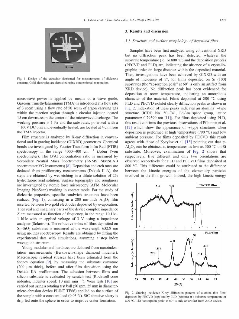
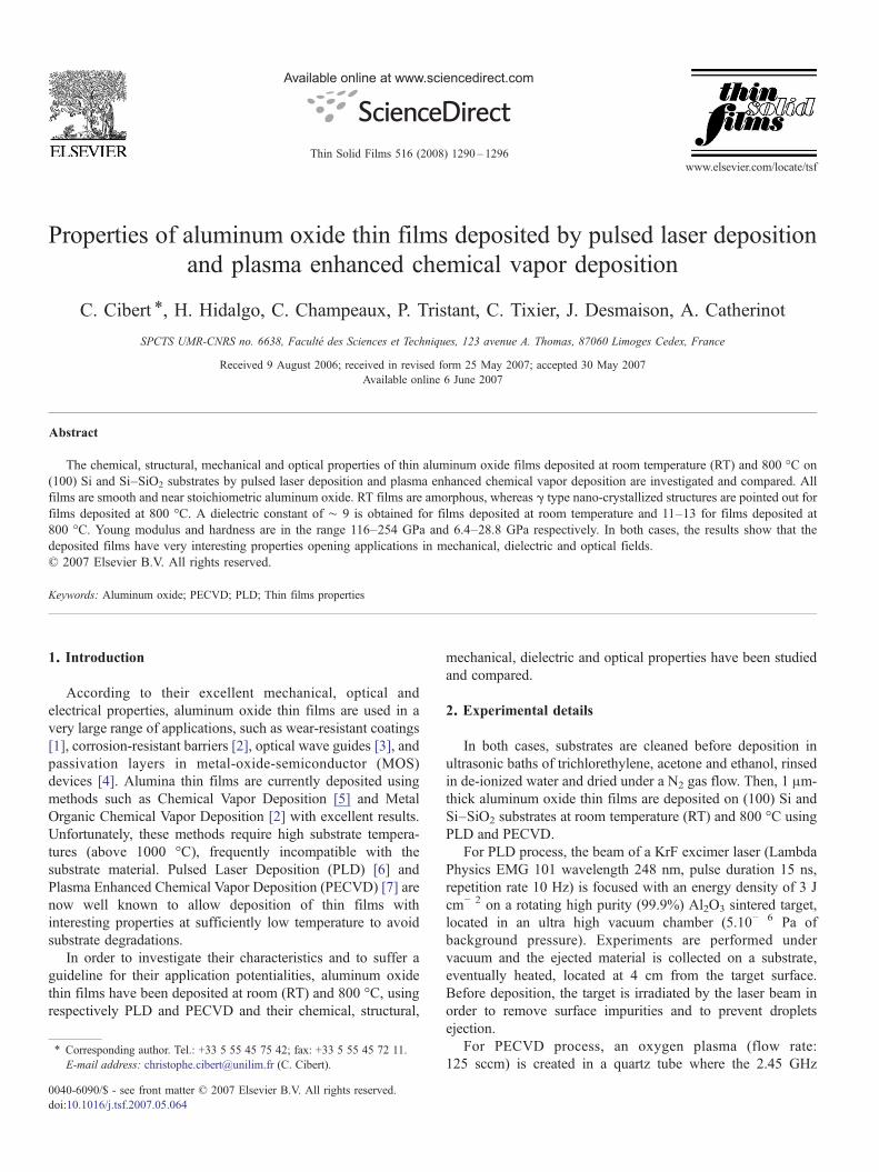
Fig. 1. Design of the capacitor fabricated for measurements of dielectricconstant. Gold electrodes are deposited using conventional evaporation.
Fig. 2. Grazing incidence X-ray diffraction patterns of alumina thin filmsdeposited by PECVD (top) and by PLD (bottom) at a substrate temperature of800 °C. The “absorption peak” at 60° is only an artifact from XRD device.
1291C. Cibert et al. / Thin Solid Films 516 (2008) 1290–1296
microwave power is applied by means of a wave guide.Gaseous trimethylaluminium (TMA) is introduced at a flow rateof 3 sccm using a flow rate of 50 sccm of argon carrying gaswithin the reaction region through a circular injector located15 cm downstream the center of the microwave discharge. Theworking pressure is 1 Pa and the substrates, polarized with a− 100V DC bias and eventually heated, are located at 4 cm fromthe TMA injector.
Film structure is analyzed by X-ray diffraction in conven-tional and in grazing incidence (GIXRD) geometries. Chemicalbonds are investigated by Fourier Transform Infra-Red (FTIR)spectroscopy in the range 4000–400 cm− 1 (Jobin Yvonspectrometer). The O/Al concentration ratio is measured bySecondary Neutral Mass Spectrometry (SNMS, SIMSLABspectrometer VG Instruments) [8]. Deposition and etch rates arededuced from profilometry measurements (Dektak II A), thesteps are obtained by wet etching in a dilute solution of 2%hydrofluoric acid solution. Surface topography and roughnessare investigated by atomic force microscopy (AFM, MolecularImaging PicoScan) working in contact mode. For the study ofdielectric properties, specific sandwich structures have beenrealized (Fig. 1), consisting in a 200 nm-thick Al2O3 filminserted between two gold electrodes deposited by evaporation.Then real and imaginary parts of the device complex impedanceZ are measured as function of frequency, in the range 10 Hz–1 kHz with an applied voltage of 3 V, using a impedanceanalyzer (Solartron). The refractive index of films deposited onSi–SiO2 substrates is measured at the wavelength 632.8 nmusing m-lines spectroscopy. Results are obtained by fitting theexperimental data with simulations, assuming a step indexwaveguide structure.
Young modulus and hardness are deduced from nanoinden-tation measurements (Berkovich-shape diamond indenter).Macroscopic residual stresses have been estimated from theStoney equation [9], by measuring the substrate curvature(200 μm thick), before and after film deposition using theDektak IIA profilometer. The adhesion between films andsilicon substrate is evaluated by scratch test (Rockwell-coneindenter, indenter speed: 10 mm min− 1). Wear tests [10] arecarried out using a rotating test ball (50 rpm, 25 mm in diameter-micro-abrasion device PLINT TE66) applied on the surface ofthe sample with a constant load (0.03 N). SiC abrasive slurry isdrip fed onto the sphere in order to improve crater formation.
3. Results and discussion
3.1. Structure and surface morphology of deposited films
Samples have been first analyzed using conventional XRDbut no diffraction peak has been detected, whatever thesubstrate temperature (RTor 800 °C) and the deposition process(PECVD and PLD) are, indicating the absence of a crystallo-graphic order on large distance within the deposited material.Then, investigations have been achieved by GIXRD with anangle of incidence of 5°, for films deposited on Si (100)substrates (the “absorption peak” at 60° is only an artifact fromXRD device). No diffraction peak has been evidenced fordeposition at room temperature, indicating an amorphouscharacter of the material. Films deposited at 800 °C usingPLD and PECVD exhibit clearly diffraction peaks as shown inFig. 2. Indexation of these peaks indicates an alumina γ-typestructure (ICDD No. 50–741, Fd-3m space group, latticeparameter: 0.79390 nm [11]). For films deposited using PLD,this result confirms the previous observations of Pillonnet et al.[12] which show the appearance of γ-type structures whendeposition is performed at high temperature (790 °C) and lowambient pressure. For films deposited by PECVD this resultagrees with those of Kyrylov et al. [13] pointing out that γ-Al2O3 can be obtained at temperatures as low as 500 °C on Sisubstrate. Moreover, examination of Fig. 2 shows thatrespectively, five different and only two orientations areobserved respectively for PLD and PECVD films deposited at800 °C. This difference could be attributed to the differencebetween the kinetic energies of the elementary particlesinvolved in the film growth. Indeed, the high kinetic energy
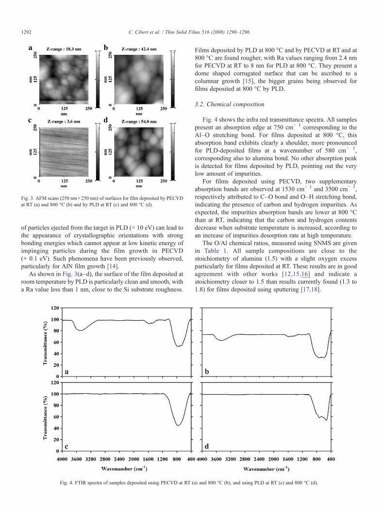
Fig. 3. AFM scans (250 nm×250 nm) of surfaces for film deposited by PECVDat RT (a) and 800 °C (b) and by PLD at RT (c) and 800 °C (d).
1292 C. Cibert et al. / Thin Solid Films 516 (2008) 1290–1296
of particles ejected from the target in PLD (≅ 10 eV) can lead tothe appearance of crystallographic orientations with strongbonding energies which cannot appear at low kinetic energy ofimpinging particles during the film growth in PECVD(≅ 0.1 eV). Such phenomena have been previously observed,particularly for AlN film growth [14].
As shown in Fig. 3(a–d), the surface of the film deposited atroom temperature by PLD is particularly clean and smooth, witha Ra value less than 1 nm, close to the Si substrate roughness.
Fig. 4. FTIR spectra of samples deposited using PECVD at RT (
Films deposited by PLD at 800 °C and by PECVD at RT and at800 °C are found rougher, with Ra values ranging from 2.4 nmfor PECVD at RT to 8 nm for PLD at 800 °C. They present adome shaped corrugated surface that can be ascribed to acolumnar growth [15], the bigger grains being observed forfilms deposited at 800 °C by PLD.
3.2. Chemical composition
Fig. 4 shows the infra red transmittance spectra. All samplespresent an absorption edge at 750 cm− 1 corresponding to theAl–O stretching bond. For films deposited at 800 °C, thisabsorption band exhibits clearly a shoulder, more pronouncedfor PLD-deposited films at a wavenumber of 580 cm− 1,corresponding also to alumina bond. No other absorption peakis detected for films deposited by PLD, pointing out the verylow amount of impurities.
For films deposited using PECVD, two supplementaryabsorption bands are observed at 1530 cm− 1 and 3500 cm− 1,respectively attributed to C–O bond and O–H stretching bond,indicating the presence of carbon and hydrogen impurities. Asexpected, the impurities absorption bands are lower at 800 °Cthan at RT, indicating that the carbon and hydrogen contentsdecrease when substrate temperature is increased, according toan increase of impurities desorption rate at high temperature.
The O/Al chemical ratios, measured using SNMS are givenin Table 1. All sample compositions are close to thestoichiometry of alumina (1.5) with a slight oxygen excessparticularly for films deposited at RT. These results are in goodagreement with other works [12,15,16] and indicate astoichiometry closer to 1.5 than results currently found (1.3 to1.8) for films deposited using sputtering [17,18].
a) and 800 °C (b), and using PLD at RT (c) and 800 °C (d).
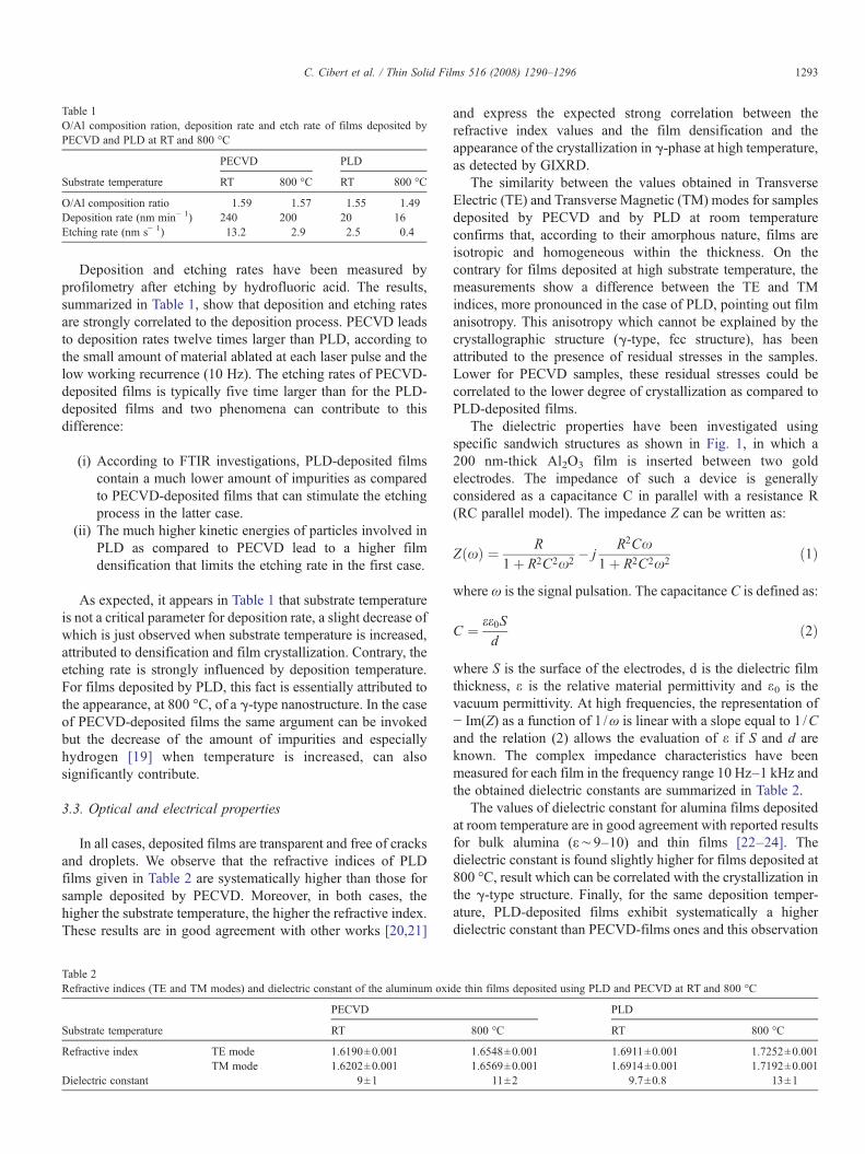
Table 1O/Al composition ration, deposition rate and etch rate of films deposited byPECVD and PLD at RT and 800 °C
PECVD PLD
Substrate temperature RT 800 °C RT 800 °C
O/Al composition ratio 1.59 1.57 1.55 1.49Deposition rate (nm min− 1) 240 200 20 16Etching rate (nm s− 1) 13.2 2.9 2.5 0.4
1293C. Cibert et al. / Thin Solid Films 516 (2008) 1290–1296
Deposition and etching rates have been measured byprofilometry after etching by hydrofluoric acid. The results,summarized in Table 1, show that deposition and etching ratesare strongly correlated to the deposition process. PECVD leadsto deposition rates twelve times larger than PLD, according tothe small amount of material ablated at each laser pulse and thelow working recurrence (10 Hz). The etching rates of PECVD-deposited films is typically five time larger than for the PLD-deposited films and two phenomena can contribute to thisdifference:
(i) According to FTIR investigations, PLD-deposited filmscontain a much lower amount of impurities as comparedto PECVD-deposited films that can stimulate the etchingprocess in the latter case.
(ii) The much higher kinetic energies of particles involved inPLD as compared to PECVD lead to a higher filmdensification that limits the etching rate in the first case.
As expected, it appears in Table 1 that substrate temperatureis not a critical parameter for deposition rate, a slight decrease ofwhich is just observed when substrate temperature is increased,attributed to densification and film crystallization. Contrary, theetching rate is strongly influenced by deposition temperature.For films deposited by PLD, this fact is essentially attributed tothe appearance, at 800 °C, of a γ-type nanostructure. In the caseof PECVD-deposited films the same argument can be invokedbut the decrease of the amount of impurities and especiallyhydrogen [19] when temperature is increased, can alsosignificantly contribute.
3.3. Optical and electrical properties
In all cases, deposited films are transparent and free of cracksand droplets. We observe that the refractive indices of PLDfilms given in Table 2 are systematically higher than those forsample deposited by PECVD. Moreover, in both cases, thehigher the substrate temperature, the higher the refractive index.These results are in good agreement with other works [20,21]
Table 2Refractive indices (TE and TM modes) and dielectric constant of the aluminum oxi
PECVD
Substrate temperature RT
Refractive index TE mode 1.6190±0.001TM mode 1.6202±0.001
Dielectric constant 9±1
and express the expected strong correlation between therefractive index values and the film densification and theappearance of the crystallization in γ-phase at high temperature,as detected by GIXRD.
The similarity between the values obtained in TransverseElectric (TE) and Transverse Magnetic (TM) modes for samplesdeposited by PECVD and by PLD at room temperatureconfirms that, according to their amorphous nature, films areisotropic and homogeneous within the thickness. On thecontrary for films deposited at high substrate temperature, themeasurements show a difference between the TE and TMindices, more pronounced in the case of PLD, pointing out filmanisotropy. This anisotropy which cannot be explained by thecrystallographic structure (γ-type, fcc structure), has beenattributed to the presence of residual stresses in the samples.Lower for PECVD samples, these residual stresses could becorrelated to the lower degree of crystallization as compared toPLD-deposited films.
The dielectric properties have been investigated usingspecific sandwich structures as shown in Fig. 1, in which a200 nm-thick Al2O3 film is inserted between two goldelectrodes. The impedance of such a device is generallyconsidered as a capacitance C in parallel with a resistance R(RC parallel model). The impedance Z can be written as:
ZðxÞ ¼ R1þ R2C2x2
� jR2Cx
1þ R2C2x2ð1Þ
where ω is the signal pulsation. The capacitance C is defined as:
C ¼ ee0Sd
ð2Þ
where S is the surface of the electrodes, d is the dielectric filmthickness, ε is the relative material permittivity and ε0 is thevacuum permittivity. At high frequencies, the representation of− Im(Z) as a function of 1 /ω is linear with a slope equal to 1 /Cand the relation (2) allows the evaluation of ε if S and d areknown. The complex impedance characteristics have beenmeasured for each film in the frequency range 10 Hz–1 kHz andthe obtained dielectric constants are summarized in Table 2.
The values of dielectric constant for alumina films depositedat room temperature are in good agreement with reported resultsfor bulk alumina (ε∼9–10) and thin films [22–24]. Thedielectric constant is found slightly higher for films deposited at800 °C, result which can be correlated with the crystallization inthe γ-type structure. Finally, for the same deposition temper-ature, PLD-deposited films exhibit systematically a higherdielectric constant than PECVD-films ones and this observation
de thin films deposited using PLD and PECVD at RT and 800 °C
PLD
800 °C RT 800 °C
1.6548±0.001 1.6911±0.001 1.7252±0.0011.6569±0.001 1.6914±0.001 1.7192±0.001
11±2 9.7±0.8 13±1
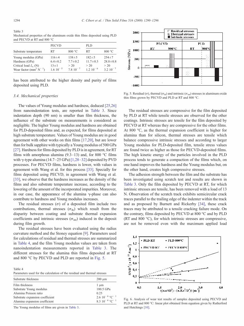
Fig. 5. Residual (σ), thermal (σth) and intrinsic (σint) stresses in aluminum oxidethin films grown by PECVD and PLD at RT and 800 °C.
Table 3Mechanical properties of the aluminum oxide thin films deposited using PLDand PECVD at RT and 800 °C
PECVD PLD
Substrate temperature RT 800 °C RT 800 °C
Young modulus (GPa) 116±4 138±5 182±5 254±7Hardness (GPa) 6.4±0.2 7.7±0.2 11.7±0.3 28.8±0.8Critical load Lc (N) 13±1 N 20 N 20 N 20Wear factor (mm2 N− 1) 1.6 10− 5 7.8 10− 7 1.2 10− 6 3.2 10− 7
1294 C. Cibert et al. / Thin Solid Films 516 (2008) 1290–1296
has been attributed to the higher density and purity of filmsdeposited using PLD.
3.4. Mechanical properties
The values of Young modulus and hardness, deduced [25,26]from nanoindentation tests, are reported in Table 3. Sinceindentation depth (90 nm) is smaller than film thickness, theinfluence of the substrate on measurements is considered asnegligible. The higher Young modulus and hardness are obtainedfor PLD-deposited films and, as expected, for films deposited athigh substrate temperature. Values of Young modulus are in goodagreement with other works on thin films [17,20], but are lowerthan for bulk sapphirewith typically aYoungmodulus of 500GPa[27]. Hardness for films deposited by PLD is in agreement, for RTfilms with amorphous alumina (9.3–13) and, for 800 °C filmswith γ-type alumina (14.7–25 GPa) [1,28–32] deposited by PVDprocesses. For PECVD films, hardness is lower, with values inagreement with Wang et al. for this process [33]. Specially forfilms deposited using PECVD, in agreement with Wang et al.[33], we observe that the hardness increases as the density of thefilms and also substrate temperature increase, according to thelowering of the amount of the incorporated impurities. Moreover,in our case, the appearance of the alumina γ-phase can alsocontribute to hardness and Young modulus increases.
The residual stresses (σ) of a deposited film include twocontributions, thermal stresses (σth) which result from thedisparity between coating and substrate thermal expansioncoefficients and intrinsic stresses (σint) induced in the depositduring film growth.
The residual stresses have been evaluated using the radiuscurvature method and the Stoney equation [9]. Parameters usedfor calculations of residual and thermal stresses are summarizedin Table 4, and the film Young modulus values are taken fromnanoindentation measurements reported in Table 3. Thedifferent stresses for the alumina thin films deposited at RTand 800 °C by PECVD and PLD are reported in Fig. 5.
Table 4Parameters used for the calculation of the residual and thermal stresses
Substrate thickness 200 μm
Film thickness 1 μmSubstrate Young modulus 180.5 GPaAlumina Poisson ratio 0.25Substrate expansion coefficient 2.6 10− 6 °C− 1
Alumina expansion coefficient 8.3 10− 6 °C− 1
The Young modulus of films are given in Table 3.
The residual stresses are compressive for the film depositedby PLD at RT while tensile stresses are observed for the othercoatings. Intrinsic stresses are tensile for the film deposited byPECVD at RTwhereas they are compressive for the other films.At 800 °C, as the thermal expansion coefficient is higher foralumina than for silicon, thermal stresses are tensile whichbalance compressive intrinsic stresses and according to largerYoung modulus for PLD-deposited film, tensile stress valuesare found twice as higher as those for PECVD-deposited films.The high kinetic energy of the particles involved in the PLDprocess tends to generate a compaction of the films which, onone hand improves the hardness and the Young modulus but, onthe other hand, creates high compressive stresses.
The adhesion strength between the film and the substrate hasbeen investigated using scratch test and results are shown inTable 3. Only the film deposited by PECVD at RT, for whichintrinsic stresses are tensile, has been removed with a load of 13N. Observation of the scratch track exhibits semicircular cracktraces parallel to the trailing edge of the indenter within the trackand as proposed by Burnett and Rickerby [34], these cracktraces may be attributed to a tensile cracking failure mode. Onthe contrary, films deposited by PECVD at 800 °C and by PLD(RT and 800 °C), for which intrinsic stresses are compressive,are not be removed even with the maximum applied load
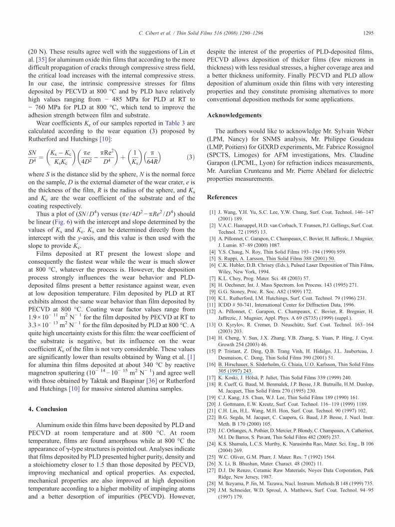
Fig. 6. Analysis of wear test results of samples deposited using PECVD andPLD at RT and 800 °C: linear plot obtained from equation given by Rutherfordand Hutchings [10].
1295C. Cibert et al. / Thin Solid Films 516 (2008) 1290–1296
(20 N). These results agree well with the suggestions of Lin etal. [35] for aluminum oxide thin films that according to the moredifficult propagation of cracks through compressive stress field,the critical load increases with the internal compressive stress.In our case, the intrinsic compressive stresses for filmsdeposited by PECVD at 800 °C and by PLD have relativelyhigh values ranging from − 485 MPa for PLD at RT to− 760 MPa for PLD at 800 °C, which tend to improve theadhesion strength between film and substrate.
Wear coefficients Kc of our samples reported in Table 3 arecalculated according to the wear equation (3) proposed byRutherford and Hutchings [10]:
SND4
¼ Ks � Kc
KsKc
� �ke4D2
� kRe2
D4
� �þ 1
Ks
� �k
64R
� �ð3Þ
where S is the distance slid by the sphere, N is the normal forceon the sample, D is the external diameter of the wear crater, e isthe thickness of the film, R is the radius of the sphere, and Ks
and Kc are the wear coefficient of the substrate and of thecoating respectively.
Thus a plot of (SN /D4) versus (πe / 4D2−πRe2 /D4) shouldbe linear (Fig. 6) with the intercept and slope determined by thevalues of Ks and Kc. Ks can be determined directly from theintercept with the y-axis, and this value is then used with theslope to provide Kc.
Films deposited at RT present the lowest slope andconsequently the fastest wear while the wear is much slowerat 800 °C, whatever the process is. However, the depositionprocess strongly influences the wear behavior and PLD-deposited films present a better resistance against wear, evenat low deposition temperature. Film deposited by PLD at RTexhibits almost the same wear behavior than film deposited byPECVD at 800 °C. Coating wear factor values range from1.9×10− 11 m2 N− 1 for the film deposited by PECVD at RT to3.3×10− 13 m2 N− 1 for the film deposited by PLD at 800 °C. Aquite high uncertainty exists for this film: the wear coefficient ofthe substrate is negative, but its influence on the wearcoefficient Kc of the film is not very considerable. These valuesare significantly lower than results obtained by Wang et al. [1]for alumina thin films deposited at about 340 °C by reactivemagnetron sputtering (10− 14−10− 15 m2 N− 1) and agree wellwith those obtained by Taktak and Baspinar [36] or Rutherfordand Hutchings [10] for massive sintered alumina samples.
4. Conclusion
Aluminum oxide thin films have been deposited by PLD andPECVD at room temperature and at 800 °C. At roomtemperature, films are found amorphous while at 800 °C theappearance of γ-type structures is pointed out. Analyses indicatethat films deposited by PLD presented higher purity, density anda stoichiometry closer to 1.5 than those deposited by PECVD,improving mechanical and optical properties. As expected,mechanical properties are also improved at high depositiontemperature according to a higher mobility of impinging atomsand a better desorption of impurities (PECVD). However,
despite the interest of the properties of PLD-deposited films,PECVD allows deposition of thicker films (few microns inthickness) with less residual stresses, a higher coverage area anda better thickness uniformity. Finally PECVD and PLD allowdeposition of aluminum oxide thin films with very interestingproperties and they constitute promising alternatives to moreconventional deposition methods for some applications.
Acknowledgements
The authors would like to acknowledge Mr. Sylvain Weber(LPM, Nancy) for SNMS analysis, Mr. Philippe Goudeau(LMP, Poitiers) for GIXRD experiments, Mr. Fabrice Rossignol(SPCTS, Limoges) for AFM investigations, Mrs. ClaudineGarapon (LPCML, Lyon) for refraction indices measurements,Mr. Aurelian Crunteanu and Mr. Pierre Abélard for dielectricproperties measurements.
References
[1] J. Wang, Y.H. Yu, S.C. Lee, Y.W. Chung, Surf. Coat. Technol. 146–147(2001) 189.
[2] V.A.C. Haanappel, H.D. van Corbach, T. Fransen, P.J. Gellings, Surf. Coat.Technol. 72 (1995) 13.
[3] A. Pillonnet, C. Garapon, C. Champeaux, C. Bovier, H. Jaffrezic, J. Mugnier,J. Lumin. 87–89 (2000) 1087.
[4] Y.S. Chaug, N. Roy, Thin Solid Films 193–194 (1990) 959.[5] S. Ruppi, A. Larsson, Thin Solid Films 388 (2001) 50.[6] C.K. Hubler, D.B. Chrisey (Eds.), Pulsed Laser Deposition of Thin Films,
Wiley, New York, 1994.[7] K.L. Choy, Prog. Mater. Sci. 48 (2003) 57.[8] H. Oechsner, Int. J. Mass Spectrom. Ion Process. 143 (1995) 271.[9] G.G. Stoney, Proc. R. Soc. A82 (1909) 172.[10] K.L. Rutherford, I.M. Hutchings, Surf. Coat. Technol. 79 (1996) 231.[11] ICDD # 50-741, International Center for Diffraction Data, 1996.[12] A. Pillonnet, C. Garapon, C. Champeaux, C. Bovier, R. Bregnier, H.
Jaffrezic, J. Mugnier, Appl. Phys. A 69 (S735) (1999) (suppl.).[13] O. Kyrylov, R. Cremer, D. Neuschütz, Surf. Coat. Technol. 163–164
(2003) 203.[14] H. Cheng, Y. Sun, J.X. Zhang, Y.B. Zhang, S. Yuan, P. Hing, J. Cryst.
Growth 254 (2003) 46.[15] P. Tristant, Z. Ding, Q.B. Trang Vinh, H. Hidalgo, J.L. Jauberteau, J.
Desmaison, C. Dong, Thin Solid Films 390 (2001) 51.[16] B. Hirschauer, S. Söderholm, G. Chiaia, U.O. Karlsson, Thin Solid Films
305 (1997) 243.[17] K. Koski, J. Hölsä, P. Juliet, Thin Solid Films 339 (1999) 240.[18] R. Cueff, G. Baud, M. Benmalek, J.P. Besse, J.R. Butruille, H.M. Dunlop,
M. Jacquet, Thin Solid Films 270 (1995) 230.[19] C.J. Kang, J.S. Chun, W.J. Lee, Thin Solid Films 189 (1990) 161.[20] J. Gottmann, E.W. Kreutz, Surf. Coat. Technol. 116–119 (1999) 1189.[21] C.H. Lin, H.L. Wang, M.H. Hon, Surf. Coat. Technol. 90 (1997) 102.[22] B.G. Segda, M. Jacquet, C. Caapera, G. Baud, J.P. Besse, J. Nucl. Instr.
Meth. B 170 (2000) 105.[23] J.C.Orlianges,A. Pothier,D.Mercier, P.Blondy,C.Champeaux,A.Catherinot,
M.I. De Barros, S. Pavant, Thin Solid Films 482 (2005) 237.[24] K.S. Shamala, L.C.S. Murthy, K. Narasimha Rao, Mater. Sci. Eng., B 106
(2004) 269.[25] W.C. Oliver, G.M. Pharr, J. Mater. Res. 7 (1992) 1564.[26] X. Li, B. Bhushan, Mater. Charact. 48 (2002) 11.[27] D.J. De Renzo, Ceramic Raw Materials, Noyes Data Corporation, Park
Ridge, New Jersey, 1987.[28] M. Ikeyama, P. Jin, M. Tazawa, Nucl. Instrum. Methods B 148 (1999) 735.[29] J.M. Schneider, W.D. Sproul, A. Matthews, Surf. Coat. Technol. 94–95
(1997) 179.

1296 C. Cibert et al. / Thin Solid Films 516 (2008) 1290–1296
[30] C. Taschner, B. Ljungberg, I. Endler, A. Leonhardt, Surf. Coat. Technol.116–119 (1999) 891.
[31] J.C. Barbour, J.A. Knapp, D.M. Follstaedt, T.M. Mayer, K.G. Minor, D.L.Linam, Nucl. Instrum. Methods B 166–167 (2000) 140.
[32] S. Nakao, P. Jin, D. Music, U. Helmersson, M. Ikeyama, Y. Miyagawa, S.Miyagawa, Surf. Coat. Technol. 158–159 (2002) 534.
[33] H.L. Wang, C.H. Lin, M.H. Hon, Thin Solid Films 310 (1997) 260.[34] P.J. Burnett, D.S. Rickerby, Thin Solid Films 154 (1987) 403.[35] C.H. Lin, H.L. Wang, M.H. Hon, Thin Solid Films 283 (1996) 171.[36] S. Taktak, M.S. Baspinar, Mater. Des. 26 (2005) 459.
Related Documents
![pH effects on novel SERS active substrateswwgis.ipcf.cnr.it/poster/3.pdf · Gold and Silver Nanoparticles obtained from Pulsed Laser Deposition (PLD)[1-3] have been deposited on glass](https://static.cupdf.com/doc/110x72/5e71059ae508f45e976bcfed/ph-effects-on-novel-sers-active-gold-and-silver-nanoparticles-obtained-from-pulsed.jpg)