This journal is © The Royal Society of Chemistry 2016 J. Mater. Chem. C, 2016, 4, 8859--8878 | 8859 Cite this: J. Mater. Chem. C, 2016, 4, 8859 Progress in pulsed laser deposited two- dimensional layered materials for device applications Zhibin Yang ab and Jianhua Hao* ab During the past decades, atomically thin, two-dimensional (2D) layered materials have been intriguing researchers for both fundamental study and practical applications, because of their extraordinary mechanical, thermal, electrical and optical properties, which are distinct from their counterparts in bulk materials. To realize the device demonstration based on 2D materials, some methods to produce 2D layers have been developed, such as mechanical exfoliation, solution based exfoliation, chemical vapour deposition (CVD) and so on. Among these methods, the physical bottom-up synthesis technique, namely pulsed laser deposition (PLD), routinely used for growing complex oxide thin films has been proved to be an alternative way to the most reported CVD method for obtaining ultrathin 2D layered films, because of its remarkable advantages. In this review, recent advances of preparing 2D materials by PLD are presented, including deposition processes, structure and characterization. We introduce the performance of proof-of-concept electronic or optoelectronic devices based on various kinds of 2D layers and ultrathin films grown using PLD and these include graphene, transition metal dichalcogenides, hexagonal boron nitride, gallium selenide, and black phosphorus. Some challenging issues are discussed and directions for future investigation are suggested. 1. Introduction In the past few decades, the development of information technology has been following the observation known as Moore’s law, which states that the number of transistors on a single computer chip will double every two years. 1–3 However, the prediction is getting closer to the end in recent years, because overheating of the electronic devices is unavoidable when more and more silicon (Si)-based circuits are integrated together into a tiny area, and the small sized transistors largely increase the manufacturing cost. 4–6 In order to solve these problems, a number of new materials have been explored to provide an alternative to Si, which could be fabricated into devices as fast as traditional Si-based electronics and also generate less heat. Two-dimensional (2D) material is one of most attractive materials which has been used for both fundamental study and practical applications over the past decade, and is regarded as a promising candidate for the next generation of electronics and optoelectronics at the 2D limit. 7–10 2D material is defined as atomically thin, layered crystalline sheets, with van der Waals (vdW) interactions between the layers. Graphene was the first 2D material to be discovered, which is composed of a single layer of sp 2 hybridized carbon atoms, showing excellent mechanical, thermal, electrical properties and high chemical stability and is still the leader out of all of the atomic sheets. 7,8,11–13 However, the main drawback of using graphene is the lack of an intrinsic energy band gap, which is crucial for the electronic materials used for transistor development. Thus, a fundamental problem of a graphene-based transistor is that the device remains conducting even when it is switched off. Consequently, a low on/off current ratio makes its use in digital logic devices unrealistic. This issue has motivated many researchers around world to search for other layered materials beyond graphene, which possess an energy band gap with a semiconducting nature. To date, several groups of 2D materials, including transition metal dichalcogenides (MX 2 ; TMDs), 14–16 phosphorene, 17–19 and silicone, 20,21 have shown a sizeable band gap value and good electronic properties, whereas hexagonal boron nitride (h-BN) 22,23 has promising dielectric properties for use as a gate insulator (Fig. 1a). These materials can be categorized as being 2D because they represent the thinnest isolated crystalline form, without surface dangling bonds, and have outstanding transport properties within the intralayer. 9,24 The portfolio of the novel 2D materials and their hybrid structure is still a Department of Applied Physics, The Hong Kong Polytechnic University, Hung Hom, Hong Kong, P. R. China. E-mail: [email protected] b The Hong Kong Polytechnic University, Shenzhen Research Institute, Shenzhen 518057, P. R. China Received 20th April 2016, Accepted 26th August 2016 DOI: 10.1039/c6tc01602b www.rsc.org/MaterialsC Journal of Materials Chemistry C REVIEW Open Access Article. Published on 31 August 2016. Downloaded on 02/05/2018 20:57:48. This article is licensed under a Creative Commons Attribution-NonCommercial 3.0 Unported Licence. View Article Online View Journal | View Issue

Welcome message from author
This document is posted to help you gain knowledge. Please leave a comment to let me know what you think about it! Share it to your friends and learn new things together.
Transcript
This journal is©The Royal Society of Chemistry 2016 J. Mater. Chem. C, 2016, 4, 8859--8878 | 8859
Cite this: J.Mater. Chem. C, 2016,
4, 8859
Progress in pulsed laser deposited two-dimensional layered materials for deviceapplications
Zhibin Yangab and Jianhua Hao*ab
During the past decades, atomically thin, two-dimensional (2D) layered materials have been intriguing
researchers for both fundamental study and practical applications, because of their extraordinary
mechanical, thermal, electrical and optical properties, which are distinct from their counterparts in bulk
materials. To realize the device demonstration based on 2D materials, some methods to produce 2D
layers have been developed, such as mechanical exfoliation, solution based exfoliation, chemical vapour
deposition (CVD) and so on. Among these methods, the physical bottom-up synthesis technique,
namely pulsed laser deposition (PLD), routinely used for growing complex oxide thin films has been
proved to be an alternative way to the most reported CVD method for obtaining ultrathin 2D layered
films, because of its remarkable advantages. In this review, recent advances of preparing 2D materials by
PLD are presented, including deposition processes, structure and characterization. We introduce the
performance of proof-of-concept electronic or optoelectronic devices based on various kinds of 2D
layers and ultrathin films grown using PLD and these include graphene, transition metal dichalcogenides,
hexagonal boron nitride, gallium selenide, and black phosphorus. Some challenging issues are discussed
and directions for future investigation are suggested.
1. Introduction
In the past few decades, the development of informationtechnology has been following the observation known asMoore’s law, which states that the number of transistors on asingle computer chip will double every two years.1–3 However,the prediction is getting closer to the end in recent years,because overheating of the electronic devices is unavoidablewhen more and more silicon (Si)-based circuits are integratedtogether into a tiny area, and the small sized transistors largelyincrease the manufacturing cost.4–6 In order to solve theseproblems, a number of new materials have been explored toprovide an alternative to Si, which could be fabricated intodevices as fast as traditional Si-based electronics and alsogenerate less heat.
Two-dimensional (2D) material is one of most attractivematerials which has been used for both fundamental studyand practical applications over the past decade, and is regardedas a promising candidate for the next generation of electronicsand optoelectronics at the 2D limit.7–10 2D material is defined
as atomically thin, layered crystalline sheets, with van der Waals(vdW) interactions between the layers. Graphene was the first 2Dmaterial to be discovered, which is composed of a single layer ofsp2 hybridized carbon atoms, showing excellent mechanical,thermal, electrical properties and high chemical stability andis still the leader out of all of the atomic sheets.7,8,11–13 However,the main drawback of using graphene is the lack of an intrinsicenergy band gap, which is crucial for the electronic materialsused for transistor development. Thus, a fundamental problemof a graphene-based transistor is that the device remainsconducting even when it is switched off. Consequently, a lowon/off current ratio makes its use in digital logic devicesunrealistic. This issue has motivated many researchers aroundworld to search for other layered materials beyond graphene,which possess an energy band gap with a semiconducting nature.To date, several groups of 2D materials, including transitionmetal dichalcogenides (MX2; TMDs),14–16 phosphorene,17–19
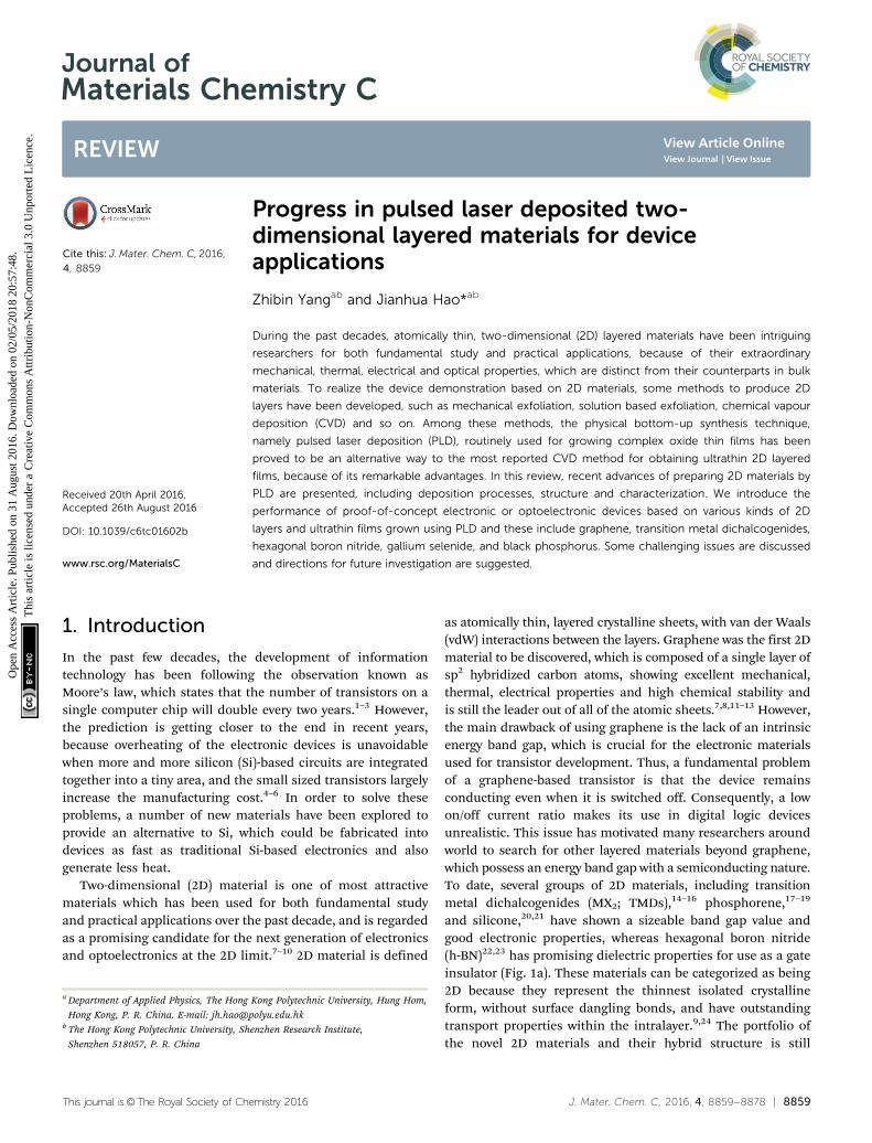
and silicone,20,21 have shown a sizeable band gap value andgood electronic properties, whereas hexagonal boron nitride(h-BN)22,23 has promising dielectric properties for use as a gateinsulator (Fig. 1a). These materials can be categorized as being2D because they represent the thinnest isolated crystallineform, without surface dangling bonds, and have outstandingtransport properties within the intralayer.9,24 The portfolio ofthe novel 2D materials and their hybrid structure is still
a Department of Applied Physics, The Hong Kong Polytechnic University, Hung Hom,
Hong Kong, P. R. China. E-mail: [email protected] The Hong Kong Polytechnic University, Shenzhen Research Institute,
Shenzhen 518057, P. R. China
Received 20th April 2016,Accepted 26th August 2016
DOI: 10.1039/c6tc01602b
www.rsc.org/MaterialsC
Journal ofMaterials Chemistry C
REVIEW
Ope
n A
cces
s A
rtic
le. P
ublis
hed
on 3
1 A
ugus
t 201
6. D
ownl
oade
d on
02/
05/2
018
20:5
7:48
. T
his
artic
le is
lice
nsed
und
er a
Cre
ativ
e C
omm
ons
Attr
ibut
ion-
Non
Com
mer
cial
3.0
Unp
orte
d L
icen
ce.
View Article OnlineView Journal | View Issue
8860 | J. Mater. Chem. C, 2016, 4, 8859--8878 This journal is©The Royal Society of Chemistry 2016
growing, arousing a technology evolution of almost everythingrelated to energy, electronics and photonics.6,25 Compared tothe Si routinely employed in modern electronics, 2D materialshave the advantages of occupying a small space and have asmaller energy consumption. Furthermore, when the thicknessof these materials is reduced to few layers, spintronics, namelythe transfer process involved by electron spins rather than theflow of charge carriers, could be considered for designing somenovel transistors.26–28
Up to now, most of the work reported on 2D materials hasbeen conducted on the basis of research laboratory fabricationand testing. To satisfy the requirement of device applications,numerous studies have focused extensively on exploring thefabrication methods capable of providing large scale, high yieldand low cost ultrathin 2D nanosheets. One of the commonlyused techniques in the synthesis of nanostructures is vapordeposition, which refers to the synthesis process exploitingvapor phase source materials to form solid films using con-densation or chemical reactions.29 Previous reviews on thebottom-up synthesis of 2D materials mainly refer to chemicalvapor deposition (CVD).30–32 Up to now, there has been noreview providing a comprehensive coverage of physical vapordeposition (PVD) methods for making 2D materials. Therefore,in this review, a systematic overview of the recent efforts,progress, opportunities and challenges in the fabrication of
2D layered materials using pulsed laser deposition (PLD) as oneof the typical PVD methods will be presented. Initially, theoperation principles and scope of application of PLD will bedescribed. After that, from Section 3 to Section 7, the advances inpreparing atomically thin nanosheets using PLD will be high-lighted including the synthesis process, structure and devicecharacterization, which will be illustrated based on the differenttypes of 2D materials. Lastly, some strategies in improvingthe performance of PLD grown, 2D layered films and potentialresearch directions in the future will be discussed.
2. Overview of PLD for 2D films
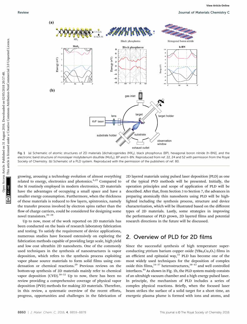
Since the successful synthesis of high temperature super-conducting yttrium barium copper oxide (YBa2Cu3O7) films inan efficient and epitaxial way,33 PLD has become one of themost widely used techniques for the deposition of complexoxide thin films,34–37 heterostructures,38–43 and well controlledinterfaces.44 As shown in Fig. 1b, the PLD system mainly consistsof an ultrahigh vacuum chamber and a high energy pulsed laser.In principle, the mechanism of PLD includes a series ofcomplex physical reactions. Briefly, when the focused laserbeam strikes the surface of a solid target for a short time, anenergetic plasma plume is formed with ions and atoms, and
Fig. 1 (a) Schematic of atomic structures of 2D materials [dichalcogenides (MX2), black phosphorus (BP), hexagonal boron nitride (h-BN)], and theelectronic band structure of monolayer molybdenum disulfide (MoS2), BP and h-BN. Reproduced from ref. 22, 24 and 52 with permission from the RoyalSociety of Chemistry. (b) Schematic of a PLD system. Reproduced with the permission of the publishers of ref. 80.
Review Journal of Materials Chemistry C
Ope
n A
cces
s A
rtic
le. P
ublis
hed
on 3
1 A
ugus
t 201
6. D
ownl
oade
d on
02/
05/2
018
20:5
7:48
. T
his
artic
le is
lice
nsed
und
er a
Cre
ativ
e C
omm
ons
Attr
ibut
ion-
Non
Com
mer
cial
3.0
Unp
orte
d L
icen
ce.
View Article Online
This journal is©The Royal Society of Chemistry 2016 J. Mater. Chem. C, 2016, 4, 8859--8878 | 8861
then collected on a pre-heated substrate placed in front of thetarget. Depending on the substrate temperature and otherfactors, a single-crystal, polycrystalline, or amorphous filmcan be obtained.45 The quality of the films deposited by PLDis strongly influenced by a number of experimental parameters.For example, the parameters of the pulsed laser source (wavelength,fluence, frequency, pulse duration, and so on) have notableeffects on the laser/target interaction.46–48 In the case of anultrashort pulse duration, such as the femtosecond (fs) laser,there is little interaction between the plume and incoming laserbecause the time for the plasma to be generated is longer thanthe pulse duration.48 Despite the attractive features of PLD, thelarge droplets induced by the laser ablation have a significantnegative impact on the surface morphology of the film. Tominimize this effect, numerous methods have been developed,such as using off-axis geometry,49 inserting a shadow mask,50
or using a dense and smooth target.51
Besides using PLD for the deposition of complex oxide thinfilms, it should be noted that PLD has been considered for usein the synthesis of layered 2D materials over recent years. Up tonow, the main techniques used for realizing mono- or few layerednanosheets include mechanical exfoliation,52–54 chemicalexfoliation,55,56 liquid-based exfoliation,57–59 CVD,30–32,60,61 andPVD.62–64 For wafer scale fabrication of 2D materials, CVD andPVD are commonly used in bottom-up techniques. The maindisadvantage of CVD is its process in harsh growth environ-ment, such as high reaction temperature and long growth time,which lead to considerable experimental difficulty. Comparingwith CVD, PVD utilizes pure physical method to prepare largescale thin films mainly under higher vacuum and lower growthtemperature. Up to now, 2D materials, including graphene,62
molybdenum disulfide (MoS2),63 molybdenum sulfoselenide(MoS2Se2)64 and so on, have been successfully realized by usingvarious PVD techniques. Compared with these methods, PLDexhibits its own features and scope of application. Table 1shows the comparison of growth conditions and materialquality for 2D materials made using different fabricationtechniques. Compared to CVD, the advantages of using PLDinclude high growth rate, low cost, good control of thicknessand morphology, and low growth temperature, and it is applic-able to versatile materials, especially for those with chemicalactive surface. In addition, it is easier to make composites usingPLD, because different targets can be installed inside thechamber simultaneously. In comparison to other PVD methods(thermal evaporation, sputtering, and so on), PLD exhibitsspecific characteristics in two important aspects. Firstly, the
synthesis is a pulsed mode, meaning that a small amountmaterial could be grown in a few microseconds. Secondly,because of the fast and strong heating of the target, stoichio-metric growth could be readily achieved by using PLD.
Further to the previous brief background information onPLD, next the preparation of atomically thin layered films usingPLD and their corresponding applications as a sequence of the2D types, including graphene, TMDs, h-BN, gallium(II) selenide(GaSe), and black phosphorus (BP), will be introduced.
3. Graphene grown using PLD
Graphene has been made using PLD since 2005, and this isearlier than the first attempt at growth using CVD in 2009.65
Cappelli et al. studied the influence of substrate temperatureon the resultant carbon films grown using PLD from a pyrolyticgraphite target.65 The Raman spectroscopy and near-edge X-rayabsorption fine structure results revealed that graphene sheetscould be obtained at 900 1C, which exhibited a trend to growalong the direction of the perpendicular to the top surface of aSi substrate. Following this work, Scilletta et al. reported thatthe formation and texture of the graphene nanosheets could beaffected by the fabrication temperature and atmosphere gas.66
According to X-ray diffraction (XRD) results, graphene nanosheetsappeared at a high temperature in vacuum. Whereas for thinfilms made in a helium gas atmosphere, only graphene particleswere characterized, which were embedded in the amorphouscarbon film. However, the thickness of the nano-grapheneobtained at this stage is about a few hundreds of a nanometerthick,67 which exceeds the scope of 2D materials.
3.1 Graphene grown on a metal substrate
Since the high quality monolayer graphene was synthesized onan iridium(111) substrate using the CVD method,68 transitionmetals have become quite commonly used substrates forfabricating graphene because of their high uniformity andease of transferring to other substrates for subsequent devicefabrication. Polycrystalline cobalt and nickel (Ni) thin films aregenerally used because of their high carbon solubility, low costand ease of fabrication into electronic devices. As the CVDmethods require a long growth time and high temperature,researchers started to consider growing graphene on metalsubstrates using PLD as an alternative to CVD.69–74 At an earlystage, Koh et al. grew graphene with a few layers (o5 layers) onNi (600 nm)/Si substrate using PLD.69 They studied the influence
Table 1 Comparison of techniques used to realize 2D materials
Size Throughput Thickness homogeneity Fabrication rate Processing temperature Ref.
Mechanical exfoliation 1–10 mm Low Low Fast RT 52–54Chemical exfoliation 1–10 mm High Moderate Moderate RT 55 and 56Liquid exfoliation 1–10 mm High Moderate Moderate RT 57–59CVD Over 10 cm High Very high Low High 30–32, 60 and 61PVD Over 10 cm High High Moderate Moderate 62–64PLD Up to 1 cm High High Fast Moderate 33–45
Journal of Materials Chemistry C Review
Ope
n A
cces
s A
rtic
le. P
ublis
hed
on 3
1 A
ugus
t 201
6. D
ownl
oade
d on
02/
05/2
018
20:5
7:48
. T
his
artic
le is
lice
nsed
und
er a
Cre
ativ
e C
omm
ons
Attr
ibut
ion-
Non
Com
mer
cial
3.0
Unp
orte
d L
icen
ce.
View Article Online
8862 | J. Mater. Chem. C, 2016, 4, 8859--8878 This journal is©The Royal Society of Chemistry 2016
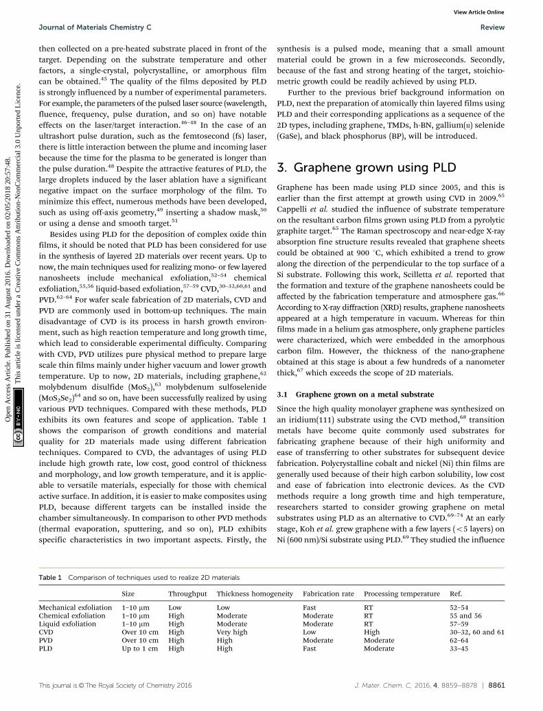
of cooling rate and laser energy on the formation and quality ofthe graphene layers. The schematic in Fig. 2a shows that themechanism of graphene layer formation on a metal substratecan be illustrated by the interactions between the carbon atomsand the metal layer.71 As the laser pulses struck the graphitetarget, the plasma plume was ejected which contained carbonions which were bombarding the substrate surface and thenpenetrated deeply into the layer of Ni. With a higher coolingrate, the carbon species were separated from Ni film because ofthe decreasing solubility of carbon in Ni. The precipitatedcarbon atoms on the Ni surface were organized to assembleinto graphene layers, and the Raman spectra shown in Fig. 2bshow this. Whereas for the synthesis process with a lowercooling rate, less carbon species were precipitated on to thesurface of the Ni film, resulting in more defects in the growngraphene film. According to the study, cooling rate is one of thekey factors in determining the quality of graphene with fewlayers grown on the metal substrates using PLD.
In a further study, Wang et al. reported that graphene withfew layers was grown on a Ni substrate under a lower tempera-ture, and the thickness of the film could be easily controlled byadjusting the proportion of the thickness of Ni to the carbonlayers.70 Ultrathin graphene films (less than five layers) weresynthesized by decreasing the carbon proportion or increasingthe initial thickness of the Ni film and the results are shown inhigh-resolution transmission electron microscopy (HRTEM)images (Fig. 2c). Apart from Ni substrates, graphene was alsorealized on some other metal substrates.71
Usually, in order to apply metal substrate based graphene todevices, a transfer process is required, which may inducedefects to the graphene film during the process and thusinfluence its electronic properties. It is notable that Hemaniet al. have developed a new method to grow graphene directlyon silicon dioxide (SiO2) substrates.72 As a catalytic layer, aNi film (300 nm) was sputtered on to SiO2 (300 nm)/Si substratefor further graphene deposition. As illustrated by scanningelectron microscopy (SEM) and Raman spectroscopy, graphenewas grown on both the Ni film surface and the Ni/SiO2 interface.By etching the Ni film off, the interfacial bilayer graphene wasdeposited directly on to the SiO2/Si substrate. High qualitygraphene synthesized by this process has been verified usingRaman mapping (Fig. 2d) and X-ray photoelectron spectroscopy(XPS) results. A similar method was applied to grow multi-layer,textured graphene films on n-doped Si substrate.75 For the firststep, an amorphous carbon film was deposited on a Ni layerbuffered Si substrate using PLD. Subsequently, the graphenewas converted from the carbon film using a post-annealingprocess. The graphene obtained could be directly used aselectrodes for electrochemical applications without needing atransfer process.
3.2 Graphene grown directly on insulating substrates
Although etching the catalytic layer can leave out the transferprocess for metal substrate based graphene, the etchant mayalso degrade the graphene layers and eventually be detrimentalto the performance of the device. Therefore, the process for
Fig. 2 (a) Illustration of the mechanism of formation of graphene. Reproduced from ref. 71 with permission from Elsevier. (b) Raman spectra of graphenedeposited with different cooling rates. Reproduced with permission of the publishers of ref. 69. (c) Cross-sectional HRTEM image of bi-layer grapheneproduced using PLD. Reproduced with permission of the publishers of ref. 70. (d) 2D mapping of intensity ratio of G to 2D Raman peaks. Reproduced withpermission of the publishers of ref. 72.
Review Journal of Materials Chemistry C
Ope
n A
cces
s A
rtic
le. P
ublis
hed
on 3
1 A
ugus
t 201
6. D
ownl
oade
d on
02/
05/2
018
20:5
7:48
. T
his
artic
le is
lice
nsed
und
er a
Cre
ativ
e C
omm
ons
Attr
ibut
ion-
Non
Com
mer
cial
3.0
Unp
orte
d L
icen
ce.
View Article Online
This journal is©The Royal Society of Chemistry 2016 J. Mater. Chem. C, 2016, 4, 8859--8878 | 8863
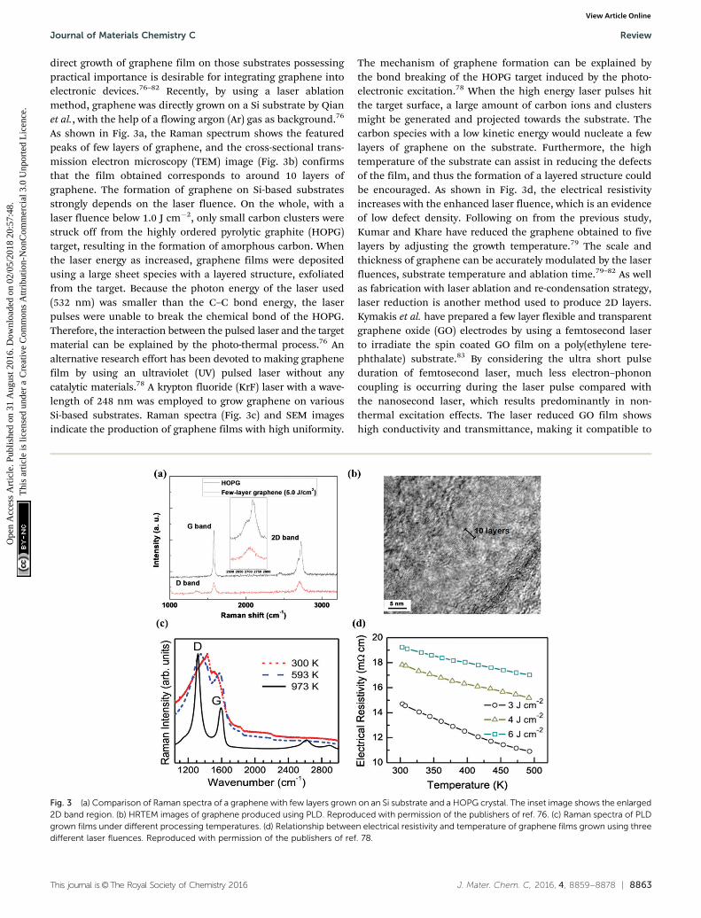
direct growth of graphene film on those substrates possessingpractical importance is desirable for integrating graphene intoelectronic devices.76–82 Recently, by using a laser ablationmethod, graphene was directly grown on a Si substrate by Qianet al., with the help of a flowing argon (Ar) gas as background.76
As shown in Fig. 3a, the Raman spectrum shows the featuredpeaks of few layers of graphene, and the cross-sectional trans-mission electron microscopy (TEM) image (Fig. 3b) confirmsthat the film obtained corresponds to around 10 layers ofgraphene. The formation of graphene on Si-based substratesstrongly depends on the laser fluence. On the whole, with alaser fluence below 1.0 J cm�2, only small carbon clusters werestruck off from the highly ordered pyrolytic graphite (HOPG)target, resulting in the formation of amorphous carbon. Whenthe laser energy as increased, graphene films were depositedusing a large sheet species with a layered structure, exfoliatedfrom the target. Because the photon energy of the laser used(532 nm) was smaller than the C–C bond energy, the laserpulses were unable to break the chemical bond of the HOPG.Therefore, the interaction between the pulsed laser and the targetmaterial can be explained by the photo-thermal process.76 Analternative research effort has been devoted to making graphenefilm by using an ultraviolet (UV) pulsed laser without anycatalytic materials.78 A krypton fluoride (KrF) laser with a wave-length of 248 nm was employed to grow graphene on variousSi-based substrates. Raman spectra (Fig. 3c) and SEM imagesindicate the production of graphene films with high uniformity.
The mechanism of graphene formation can be explained bythe bond breaking of the HOPG target induced by the photo-electronic excitation.78 When the high energy laser pulses hitthe target surface, a large amount of carbon ions and clustersmight be generated and projected towards the substrate. Thecarbon species with a low kinetic energy would nucleate a fewlayers of graphene on the substrate. Furthermore, the hightemperature of the substrate can assist in reducing the defectsof the film, and thus the formation of a layered structure couldbe encouraged. As shown in Fig. 3d, the electrical resistivityincreases with the enhanced laser fluence, which is an evidenceof low defect density. Following on from the previous study,Kumar and Khare have reduced the graphene obtained to fivelayers by adjusting the growth temperature.79 The scale andthickness of graphene can be accurately modulated by the laserfluences, substrate temperature and ablation time.79–82 As wellas fabrication with laser ablation and re-condensation strategy,laser reduction is another method used to produce 2D layers.Kymakis et al. have prepared a few layer flexible and transparentgraphene oxide (GO) electrodes by using a femtosecond laserto irradiate the spin coated GO film on a poly(ethylene tere-phthalate) substrate.83 By considering the ultra short pulseduration of femtosecond laser, much less electron–phononcoupling is occurring during the laser pulse compared withthe nanosecond laser, which results predominantly in non-thermal excitation effects. The laser reduced GO film showshigh conductivity and transmittance, making it compatible to
Fig. 3 (a) Comparison of Raman spectra of a graphene with few layers grown on an Si substrate and a HOPG crystal. The inset image shows the enlarged2D band region. (b) HRTEM images of graphene produced using PLD. Reproduced with permission of the publishers of ref. 76. (c) Raman spectra of PLDgrown films under different processing temperatures. (d) Relationship between electrical resistivity and temperature of graphene films grown using threedifferent laser fluences. Reproduced with permission of the publishers of ref. 78.
Journal of Materials Chemistry C Review
Ope
n A
cces
s A
rtic
le. P
ublis
hed
on 3
1 A
ugus
t 201
6. D
ownl
oade
d on
02/
05/2
018
20:5
7:48
. T
his
artic
le is
lice
nsed
und
er a
Cre
ativ
e C
omm
ons
Attr
ibut
ion-
Non
Com
mer
cial
3.0
Unp
orte
d L
icen
ce.
View Article Online
8864 | J. Mater. Chem. C, 2016, 4, 8859--8878 This journal is©The Royal Society of Chemistry 2016
be utilized with a flexible device. Using results from recent studiesperformed by several research groups, the growth conditions,morphology and properties of PLD grown graphene on bothmetal and insulating substrates are summarized in Table 2.
3.3 Applications of graphene grown by PLD
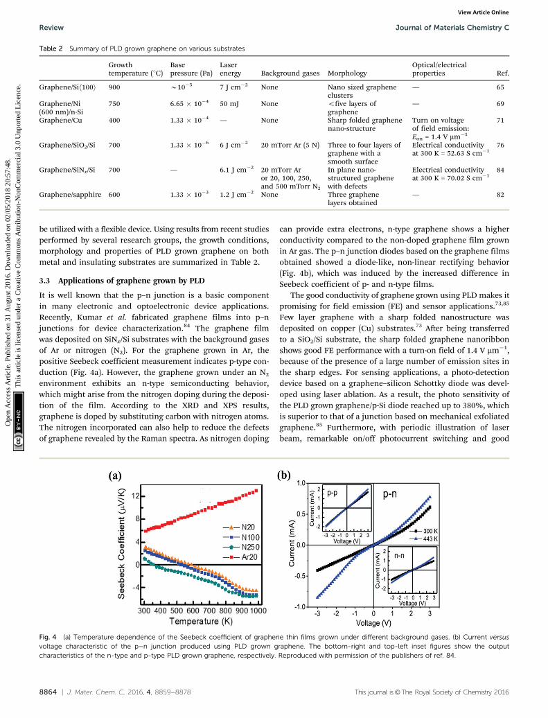
It is well known that the p–n junction is a basic componentin many electronic and optoelectronic device applications.Recently, Kumar et al. fabricated graphene films into p–njunctions for device characterization.84 The graphene filmwas deposited on SiNx/Si substrates with the background gasesof Ar or nitrogen (N2). For the graphene grown in Ar, thepositive Seebeck coefficient measurement indicates p-type con-duction (Fig. 4a). However, the graphene grown under an N2
environment exhibits an n-type semiconducting behavior,which might arise from the nitrogen doping during the deposi-tion of the film. According to the XRD and XPS results,graphene is doped by substituting carbon with nitrogen atoms.The nitrogen incorporated can also help to reduce the defectsof graphene revealed by the Raman spectra. As nitrogen doping
can provide extra electrons, n-type graphene shows a higherconductivity compared to the non-doped graphene film grownin Ar gas. The p–n junction diodes based on the graphene filmsobtained showed a diode-like, non-linear rectifying behavior(Fig. 4b), which was induced by the increased difference inSeebeck coefficient of p- and n-type films.
The good conductivity of graphene grown using PLD makes itpromising for field emission (FE) and sensor applications.73,85
Few layer graphene with a sharp folded nanostructure wasdeposited on copper (Cu) substrates.73 After being transferredto a SiO2/Si substrate, the sharp folded graphene nanoribbonshows good FE performance with a turn-on field of 1.4 V mm�1,because of the presence of a large number of emission sites inthe sharp edges. For sensing applications, a photo-detectiondevice based on a graphene–silicon Schottky diode was devel-oped using laser ablation. As a result, the photo sensitivity ofthe PLD grown graphene/p-Si diode reached up to 380%, whichis superior to that of a junction based on mechanical exfoliatedgraphene.85 Furthermore, with periodic illustration of laserbeam, remarkable on/off photocurrent switching and good
Table 2 Summary of PLD grown graphene on various substrates
Growthtemperature (1C)
Basepressure (Pa)
Laserenergy Background gases Morphology
Optical/electricalproperties Ref.
Graphene/Sih100i 900 B10�5 7 J cm�2 None Nano sized grapheneclusters
— 65
Graphene/Ni(600 nm)/n-Si
750 6.65 � 10�4 50 mJ None ofive layers ofgraphene
— 69
Graphene/Cu 400 1.33 � 10�4 — None Sharp folded graphenenano-structure
Turn on voltageof field emission:Eon = 1.4 V mm�1
71
Graphene/SiO2/Si 700 1.33 � 10�6 6 J cm�2 20 mTorr Ar (5 N) Three to four layers ofgraphene with asmooth surface
Electrical conductivityat 300 K = 52.63 S cm�1
76
Graphene/SiNx/Si 700 — 6.1 J cm�2 20 mTorr Aror 20, 100, 250,and 500 mTorr N2
In plane nano-structured graphenewith defects
Electrical conductivityat 300 K = 70.02 S cm�1
84
Graphene/sapphire 600 1.33 � 10�3 1.2 J cm�2 None Three graphenelayers obtained
— 82
Fig. 4 (a) Temperature dependence of the Seebeck coefficient of graphene thin films grown under different background gases. (b) Current versusvoltage characteristic of the p–n junction produced using PLD grown graphene. The bottom-right and top-left inset figures show the outputcharacteristics of the n-type and p-type PLD grown graphene, respectively. Reproduced with permission of the publishers of ref. 84.
Review Journal of Materials Chemistry C
Ope
n A
cces
s A
rtic
le. P
ublis
hed
on 3
1 A
ugus
t 201
6. D
ownl
oade
d on
02/
05/2
018
20:5
7:48
. T
his
artic
le is
lice
nsed
und
er a
Cre
ativ
e C
omm
ons
Attr
ibut
ion-
Non
Com
mer
cial
3.0
Unp
orte
d L
icen
ce.
View Article Online
This journal is©The Royal Society of Chemistry 2016 J. Mater. Chem. C, 2016, 4, 8859--8878 | 8865
response time were observed, indicating the potential of fastand effective photo-sensing from the graphene/p-Si diode.
Because of its high adsorption capacity, graphene has beenwidely used in applications for environmental clean-up as well.86
Recently, Tite et al. have applied the PLD grown grapheneto detect the deltamethrin concentration in cultured humankeratinocyte cells.87 Graphene with few layers was obtained bypost-annealing amorphous carbon film, which was directlydeposited on an Si substrate using PLD. Gold nanoparticles weredecorated on the graphene surface to improve the sensitivity.As a result, the Raman spectra feature peaks of graphene with anobservably enhanced intensity in the presence of increasingdeltamethrin concentrations, indicating that the insecticidecan be detected at the concentration below the cytotoxic dose.
4. 2D TMDs grown using PLD
The 2D TMDs have attracted a lot of interest because oftheir outstanding mechanical, thermal, optical and electrical proper-ties, which are distinct from their corresponding bulk materials.14–16
In recent years, MoS2 and tungsten disulfide (WS2) have been mostextensively studied for both their fundamental properties andpotential applications because of their considerable band gap and
high carrier mobility. For the time being, the synthesis of large areauniform MoS2 and WS2 thin films are mainly achieved using a CVDtechnique. In the following part of this section, the fabricationprocess and applications of MoS2 and WS2 thin films producedusing PLD as an alternative route to CVD will be reviewed.
4.1 Layered MoS2 thin films grown using PLD
The early stages of synthesis of MoS2 thin films employing pulsedlaser can be dated back to the twentieth century.88–91 As far back as1988, MoS2 thin films were deposited on stainless steel substratesusing PLD under a fairly low growth temperature (300 1C).88 Thefilms showed the same stoichiometry as the MoS2 target. However,the internal structure of the film was unknown and the thicknesswas too large compared to the scope of 2D materials.
Since MoS2 was re-evaluated and realized as a new memberof layered 2D materials, the ultrathin films of MoS2 wereobtained using PLD and the number of deposited layers can becontrolled.92–101 Loh and Chua attempted to grow MoS2 onvarious metal substrates, [aluminium, silver (Ag), Ni, Cu, and so on]which were chosen because of their smaller lattice mismatch.92
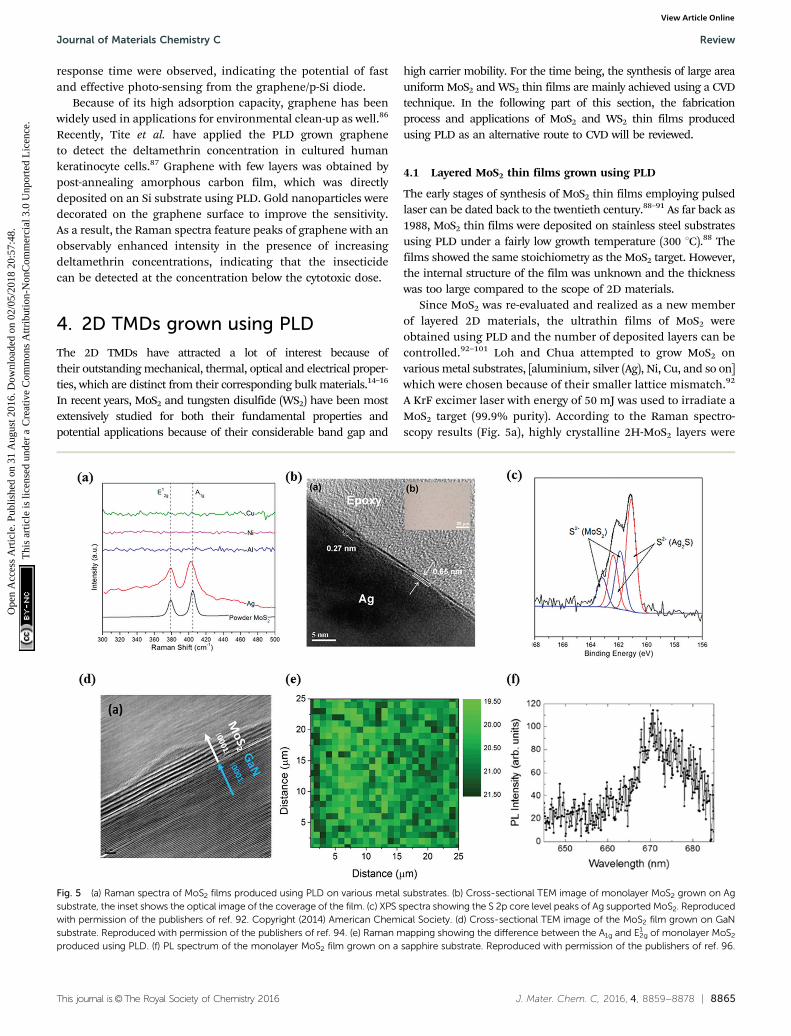
A KrF excimer laser with energy of 50 mJ was used to irradiate aMoS2 target (99.9% purity). According to the Raman spectro-scopy results (Fig. 5a), highly crystalline 2H-MoS2 layers were
Fig. 5 (a) Raman spectra of MoS2 films produced using PLD on various metal substrates. (b) Cross-sectional TEM image of monolayer MoS2 grown on Agsubstrate, the inset shows the optical image of the coverage of the film. (c) XPS spectra showing the S 2p core level peaks of Ag supported MoS2. Reproducedwith permission of the publishers of ref. 92. Copyright (2014) American Chemical Society. (d) Cross-sectional TEM image of the MoS2 film grown on GaNsubstrate. Reproduced with permission of the publishers of ref. 94. (e) Raman mapping showing the difference between the A1g and E1
2g of monolayer MoS2
produced using PLD. (f) PL spectrum of the monolayer MoS2 film grown on a sapphire substrate. Reproduced with permission of the publishers of ref. 96.
Journal of Materials Chemistry C Review
Ope
n A
cces
s A
rtic
le. P
ublis
hed
on 3
1 A
ugus
t 201
6. D
ownl
oade
d on
02/
05/2
018
20:5
7:48
. T
his
artic
le is
lice
nsed
und
er a
Cre
ativ
e C
omm
ons
Attr
ibut
ion-
Non
Com
mer
cial
3.0
Unp
orte
d L
icen
ce.
View Article Online
8866 | J. Mater. Chem. C, 2016, 4, 8859--8878 This journal is©The Royal Society of Chemistry 2016
obtained on Ag substrates only, and the film grown can be asthin as two to three layers, which was confirmed by the cross-sectional TEM image (Fig. 5b). In contrast to graphene, themechanism of MoS2 deposited using PLD is complicatedbecause two types of element atoms or clusters are generatedand the sulfur species form other compounds easier by reactingwith the metal substrate. When sulfur atoms arrive the surfaceof the Ag substrate, a layer of silver sulfide (Ag2S) is formed,which was verified by XPS results (Fig. 5c), which become anexcellent template for the growth of MoS2 thin films, which issurprising when considering the infinitesimal lattice mismatchbetween them. With high uniformity and large grain size, thequality of few layer MoS2 supported by an Ag substrate grownusing PLD is comparable to the films grown using CVD. Whereasfor other metal substrates, a native oxide layer covering the metalsurface will form an energy barrier to obstruct the crystallizationof MoS2.
Despite the metal substrates, few layer MoS2 films were alsorealized on several conventional semiconductor/insulator sub-strates using PLD.94–101 Serrao et al. have employed PLD to growMoS2 thin films on aluminium oxide (Al2O3) (0001), galliumnitride (GaN) (0001) and silicon carbide-6H (SiC-6H) (0001)substrates.94 To obtain highly crystalline films, tetrathiomolyb-date (MoS4) with an optimized stoichiometry was the target,and this resulted in sulfur-rich nanosheets. The growth tem-perature was 700 1C, which is higher than that used for thegrowth on metal substrates. The layered structure and highcrystallinity of the MoS2 thin films obtained were confirmedusing a cross-sectional TEM image (Fig. 5d) and XRD, respectively.In addition, Siegel et al. have successfully grown single layer MoS2
on a sapphire substrate, which was evident using both atomicforce microscopy (AFM) images and Raman spectroscopy map-ping (Fig. 5e).96 The photoluminescence (PL) results showedthat the obtained film had a direct band gap of 1.85 eV (Fig. 5f),which agreed with the characteristic of a monolayer MoS2
nanosheet synthesized using other methods. Recently, highlystoichiometry mono- and few layer MoS2 films were realized onvarious substrates, [sapphire, hafnium(IV) oxide (HfO2), quartzand SiO2] using PLD.101 MoS2 and S powders with an atomicratio of 1 : 1 were used as precursor materials for the targetfabrication. The results of high-resolution Rutherford backscat-tering confirm the stoichiometry synthesis of MoS2 using PLD. Itis important to note that this work reveals that the layer numberof MoS2 thin films can be accurately tuned by controlling thenumber of laser pulses.
4.2 Applications based on PLD-grown MoS2
The previously described few layer MoS2 materials obtainedusing PLD are found to possess desirable features, such as largescale, good continuity, high uniformity and fewer defects.92–101
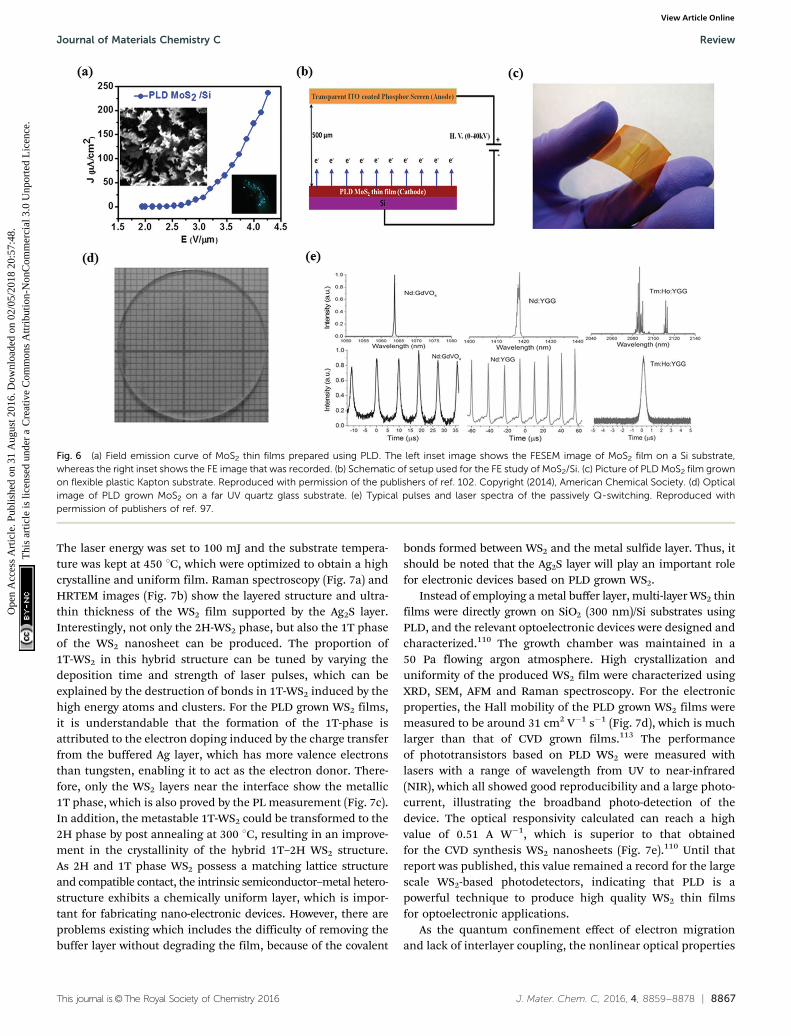
All these properties enable the MoS2 films to be applied to anumber of electronic and optoelectronic device applications.Late et al. studied the FE and photoresponse of PLD grownMoS2 thin films on various substrates, including tungsten (W)tip, Si wafer and flexible Kapton (polyimide) substrates.102
For the sample of MoS2 grown on the W tip, the SEM image
of the film surface exhibited several sharped distributed projec-tions (Fig. 6a), which may work as the intrinsic emitter tips. TheFE measurement was conducted on the MoS2/W tip, showingthe FE current density of up to 30 mA cm�2 prompted by thevoltage of 3.8 kV. The strong FE may be explained by theenhanced local electric field biased to the tip of the projectionson the film surface. In addition, good stability of the FE currentwas observed at 1 mA and no degradation of the emitter’sperformance was seen after a long measurement time. Whereasfor a few layer MoS2 grown on a Si substrate (Fig. 6b), a 1 mA cm�2
emission current density was turned on under the electric field of2 V mm�1, which is superior to the performance of MoS2 flakesobtained using a liquid method.103 The origin of this low turn-onvoltage is ascribed to the nano-scale projections on the MoS2
surface and the good electrical contacts between the thin filmsand substrates. Furthermore, the authors have measured the UVlight photoresponse of a PLD grown MoS2 film on both n and pdoped Si substrates.102 When irradiating the sample by 365 nmUV light, large photocurrents were generated, which wereinduced by the excitons from the interface of MoS2 and thesubstrates. The rectifying behavior was also recognized fromthe MoS2/p-Si heterostructure. The similar UV photoresponsewas observed from the PLD grown MoS2 thin films supportedby the flexible Kapton substrates as well (Fig. 6c).
The PLD grown MoS2 on a UV quartz glass wafer was alsodeveloped with a saturable absorber (SA), which exploits thenon-linear optical properties of MoS2.97–100 A broadband SA wasdesigned based on several narrow band-gap semiconductors,indicating that the normal MoS2 layers do not satisfy therequirements of this application. To address this issue, PLDwas employed to produce MoS2 thin films with S defects, whichwere induced by the bombardment of the energetic largeparticles generated from the pulsed laser.97 Fig. 6d shows theoptical images of PLD grown MoS2 thin film on a far UV quartzglass wafer. It should be noted that the growth temperature is aslow as 300 1C. According to the theoretical calculation, the Sdefects can reduce the band gap of few layers MoS2 from 1.08 eVto 0.08 eV, which makes it applicable for fabricating SA devices.The saturable absorption of the few layer MoS2 obtained wasmeasured by using a picoseconds Nd:YAG laser. The measuredsaturation intensity is 2.45 GW cm�2 (Fig. 6e), which is superior tothat of graphene.104,105 The MoS2 thin films were then employedas the SA for the Q-switched lasers with different wavelengths,which were characterized using a digital oscilloscope. Duringthe measurement, MoS2 layers were not damaged by the heatgenerated from the pump power, resulting in the stable outputwhile the laser was activated. Consequently, such PLD grownMoS2 shows good saturable absorption properties, which ispromising for future SA applications.
4.3 Layered WS2 thin films grown using PLD
As indicated in the literature, wafer scale, few layer WS2 havebeen deposited on various types of substrates using PLD.106–112
Similar to MoS2, a thin Ag film coated Si wafers were used assubstrates for the synthesis of high quality WS2 film, becauseof the lattice matching Ag2S formation at the interface.107,108
Review Journal of Materials Chemistry C
Ope
n A
cces
s A
rtic
le. P
ublis
hed
on 3
1 A
ugus
t 201
6. D
ownl
oade
d on
02/
05/2
018
20:5
7:48
. T
his
artic
le is
lice
nsed
und
er a
Cre
ativ
e C
omm
ons
Attr
ibut
ion-
Non
Com
mer
cial
3.0
Unp
orte
d L
icen
ce.
View Article Online
This journal is©The Royal Society of Chemistry 2016 J. Mater. Chem. C, 2016, 4, 8859--8878 | 8867
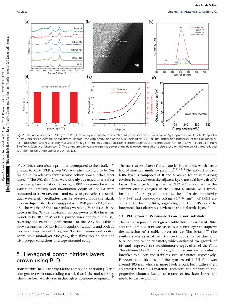
The laser energy was set to 100 mJ and the substrate tempera-ture was kept at 450 1C, which were optimized to obtain a highcrystalline and uniform film. Raman spectroscopy (Fig. 7a) andHRTEM images (Fig. 7b) show the layered structure and ultra-thin thickness of the WS2 film supported by the Ag2S layer.Interestingly, not only the 2H-WS2 phase, but also the 1T phaseof the WS2 nanosheet can be produced. The proportion of1T-WS2 in this hybrid structure can be tuned by varying thedeposition time and strength of laser pulses, which can beexplained by the destruction of bonds in 1T-WS2 induced by thehigh energy atoms and clusters. For the PLD grown WS2 films,it is understandable that the formation of the 1T-phase isattributed to the electron doping induced by the charge transferfrom the buffered Ag layer, which has more valence electronsthan tungsten, enabling it to act as the electron donor. There-fore, only the WS2 layers near the interface show the metallic1T phase, which is also proved by the PL measurement (Fig. 7c).In addition, the metastable 1T-WS2 could be transformed to the2H phase by post annealing at 300 1C, resulting in an improve-ment in the crystallinity of the hybrid 1T–2H WS2 structure.As 2H and 1T phase WS2 possess a matching lattice structureand compatible contact, the intrinsic semiconductor–metal hetero-structure exhibits a chemically uniform layer, which is impor-tant for fabricating nano-electronic devices. However, there areproblems existing which includes the difficulty of removing thebuffer layer without degrading the film, because of the covalent
bonds formed between WS2 and the metal sulfide layer. Thus, itshould be noted that the Ag2S layer will play an important rolefor electronic devices based on PLD grown WS2.
Instead of employing a metal buffer layer, multi-layer WS2 thinfilms were directly grown on SiO2 (300 nm)/Si substrates usingPLD, and the relevant optoelectronic devices were designed andcharacterized.110 The growth chamber was maintained in a50 Pa flowing argon atmosphere. High crystallization anduniformity of the produced WS2 film were characterized usingXRD, SEM, AFM and Raman spectroscopy. For the electronicproperties, the Hall mobility of the PLD grown WS2 films weremeasured to be around 31 cm2 V�1 s�1 (Fig. 7d), which is muchlarger than that of CVD grown films.113 The performanceof phototransistors based on PLD WS2 were measured withlasers with a range of wavelength from UV to near-infrared(NIR), which all showed good reproducibility and a large photo-current, illustrating the broadband photo-detection of thedevice. The optical responsivity calculated can reach a highvalue of 0.51 A W�1, which is superior to that obtainedfor the CVD synthesis WS2 nanosheets (Fig. 7e).110 Until thatreport was published, this value remained a record for the largescale WS2-based photodetectors, indicating that PLD is apowerful technique to produce high quality WS2 thin filmsfor optoelectronic applications.
As the quantum confinement effect of electron migrationand lack of interlayer coupling, the nonlinear optical properties
Fig. 6 (a) Field emission curve of MoS2 thin films prepared using PLD. The left inset image shows the FESEM image of MoS2 film on a Si substrate,whereas the right inset shows the FE image that was recorded. (b) Schematic of setup used for the FE study of MoS2/Si. (c) Picture of PLD MoS2 film grownon flexible plastic Kapton substrate. Reproduced with permission of the publishers of ref. 102. Copyright (2014), American Chemical Society. (d) Opticalimage of PLD grown MoS2 on a far UV quartz glass substrate. (e) Typical pulses and laser spectra of the passively Q-switching. Reproduced withpermission of publishers of ref. 97.
Journal of Materials Chemistry C Review
Ope
n A
cces
s A
rtic
le. P
ublis
hed
on 3
1 A
ugus
t 201
6. D
ownl
oade
d on
02/
05/2
018
20:5
7:48
. T
his
artic
le is
lice
nsed
und
er a
Cre
ativ
e C
omm
ons
Attr
ibut
ion-
Non
Com
mer
cial
3.0
Unp
orte
d L
icen
ce.
View Article Online
8868 | J. Mater. Chem. C, 2016, 4, 8859--8878 This journal is©The Royal Society of Chemistry 2016
of 2D TMD materials are prominent compared to their bulks.114
Similar to MoS2, PLD grown WS2 was also exploited to be SAsfor a dual-wavelength femtosecond soliton mode-locked fiberlaser.112 The WS2 thin films were directly deposited onto a fibertaper using laser ablation. By using a 1550 nm pump laser, thesaturation intensity and modulation depth of the SA weremeasured to be 20 MW cm�2 and 0.7%, respectively. The stabledual wavelength oscillation can be observed from the highlyerbium-doped fiber laser equipped with PLD grown WS2-basedSA. The widths of the laser pulses were 585 fs and 605 fs. Asshown in Fig. 7f, the maximum output power of the laser wasfound to be 10.1 mW with a pulsed laser energy of 1.14 nJ,revealing the excellent performance of the WS2 SA. Table 3shows a summary of fabrication conditions, quality and optical/electrical properties of PLD-grown TMDs on various substrates.Large scale monolayer MoS2/WS2 thin films can be obtainedwith proper conditions and experimental setup.
5. Hexagonal boron nitrides layersgrown using PLD
Born nitride (BN) is the crystalline compound of boron (B) andnitrogen (N) with outstanding chemical and thermal stability,which has been widely used in the high temperature equipment.115
The most stable phase of this material is the h-BN, which has alayered structure similar to graphite.23,116–118 The network of eachh-BN layer is composed of B and N atoms bound with strongcovalent bonds, whereas the adjacent layers are held by weak vdWforces. The large band gap value (5.97 eV) is induced by thedifferent on-site energies of the B and N atoms. As a typicalinsulator of 2D layered materials, the dielectric permittivity(e = 3–4) and breakdown voltage (0.7 V nm�1) of h-BN aresuperior to those of SiO2, suggesting that the h-BN could beintegrated into electronic devices as the dielectric layer.23
5.1 PLD grown h-BN nanosheets on various substrates
The earlier report on PLD grown h-BN thin film is dated 1999,and the obtained film was used as a buffer layer to improvethe adhesion of a cubic boron nitride film (c-BN).119 Thesynthesis was assisted with the continuous bombardment ofN or Ar ions to the substrate, which activated the growth ofBN and improved the stoichiometric replication of the film.The obtained h-BN film shows good adhesion and a uniforminterface to silicon and stainless steel substrates, respectively.However, the thickness of the synthesized h-BN film wasaround 100 nm, which is more likely a bulk form rather thanan atomically thin 2D material. Therefore, the fabrication andproperties characterization of mono- or few layer h-BN stillneeds further exploration.
Fig. 7 (a) Raman spectra of PLD-grown WS2 films on Ag and sapphire substrates. (b) Cross-sectional TEM image of Ag supported thin films. (c) PL spectraof WS2 thin films grown on Ag substrates. Reproduced with permission of the publishers of ref. 107. (d) The distribution histogram of the Hall mobility.(e) Photocurrent and responsivity versus bias voltage for the WS2 phototransistor in ambient conditions. Reproduced from ref. 110 with permission fromThe Royal Society of Chemistry. (f) The output power versus the pump power of the dual wavelength soliton pulse based on PLD grown WS2. Reproducedwith permission of the publishers of ref. 112.
Review Journal of Materials Chemistry C
Ope
n A
cces
s A
rtic
le. P
ublis
hed
on 3
1 A
ugus
t 201
6. D
ownl
oade
d on
02/
05/2
018
20:5
7:48
. T
his
artic
le is
lice
nsed
und
er a
Cre
ativ
e C
omm
ons
Attr
ibut
ion-
Non
Com
mer
cial
3.0
Unp
orte
d L
icen
ce.
View Article Online
This journal is©The Royal Society of Chemistry 2016 J. Mater. Chem. C, 2016, 4, 8859--8878 | 8869
Recently, ultrathin h-BN films were successfully produced byusing a high repetition laser on Mo, aluminum nitride (AIN)and Si substrates.120–125 A high purity pyrolytic h-BN crystalwith a boron to nitride atom ratio of 1.05 was used as the target.The growth temperature showed a significant influence onthe crystalline structure of BN films, in which the proportionof h-BN increases together with a decrease of the substratetemperature.126–128 One possible reason for this is that the hightemperature will increase the internal stress and thermal vibra-tions of the film, resulting in the phase transition to c-BN.Interestingly, the pure h-BN nanosheets can be obtained atsubstrate temperature of 450 1C, which is much lower than thatof CVD based fabrication. The high uniformity, good crystallinityand high transparency of h-BN films were confirmed using TEMand Raman spectroscopy (Fig. 8a). From the magnified HRTEMimage (Fig. 8b), the highly ordered honeycomb structure canbe observed and the distance between B and N atoms is about1.45 Å. The possibility of N–N and B–B bonds can also be excluded.Furthermore, different types of substrate supported h-BN filmshow a similar structure and morphology. Therefore, the h-BNnanosheets are formed before arriving at the substrate surface,which is evidence that the nanosheets’ exfoliation was inducedby laser energy from the bulk target. It should be noted that thelaser induced high energy particles, molecular or clusters willbring defects and contaminations to the film surface. Sajjad et al.have shown that growth in a hydrogen (H2) environment caneffectively reduce the impurities of the h-BN film.122 Theinteraction between plasma ions and H2 molecules can reducethe energy of particulates in the plasma, which will weaken theside effects of sputtering. Furthermore, the H ions generatedfrom the collision can help to etch the B–O components,resulting in high purity and defect free h-BN films.
The electrical properties of h-BN nanosheets with few layerswere studied using different thicknesses and temperatures, andthis revealed that the electrical conductivity of h-BN layersstrongly depends on the directions of the measurements, whichcan be explained by the quantum confinement effect (Fig. 8c). Itshowed that the electrical resistivity of h-BN sheets decreasedtogether with the decrease of layer numbers when observedfrom the longitudinal direction, and the ultrathin h-BN pre-sented metal-like properties, which had a large deviation fromits bulk. Whereas the measurement temperature was increasedfrom 25 1C to 200 1C, the conductivity of h-BN sheets with fewlayers was almost fixed along the longitudinal direction. Althoughthe defect free, single crystalline h-BP with few layers weresynthesized using PLD, the lateral size of each h-BN nanosheetis only a few micrometers, which resulted in the poor uniformityand morphology over large areas, limiting its applications as adielectric layer to wafer scale graphene-based devices.
In an alternative study, Glavin et al. reported that the poly-crystalline h-BN film was epitaxially grown on HOPG substrate,which had a similar lattice parameter to the h-BN crystal.129,130
In contrast to the previously reported experiment design, anamorphous BN bulk was used as the target in this study, andthe growth temperature was raised up to 700 1C. A flowing highpurity N2 was introduced as the operation gas, which couldstrongly affect the composition of the film. The collisionsbetween plasma and background gas result in high concentra-tions of boron ions and nitrogen. With an optimized target–substrate distance and background pressure, stoichiometrich-BN films possessing high uniformity can be obtained by recom-bining boron ions and neutral atomic nitrogen. In addition, asthe collision with the background gas decelerates the plasmaplume, it can help to reduce the kinetic energy of the energetic
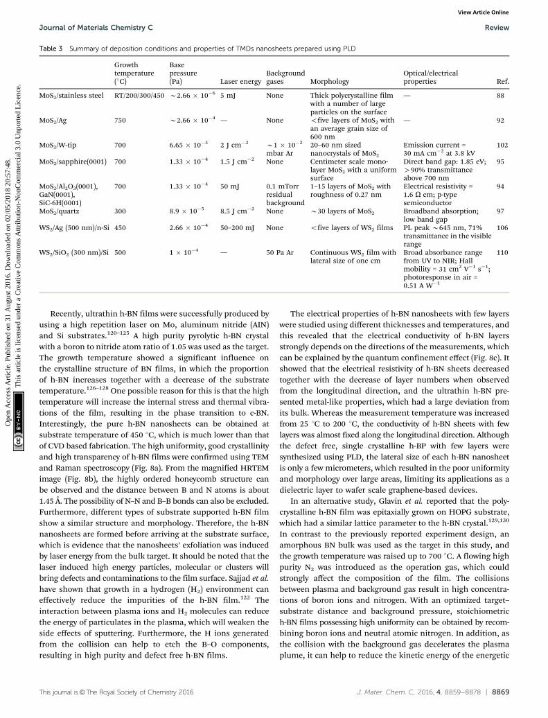
Table 3 Summary of deposition conditions and properties of TMDs nanosheets prepared using PLD
Growthtemperature(1C)
Basepressure(Pa) Laser energy
Backgroundgases Morphology
Optical/electricalproperties Ref.
MoS2/stainless steel RT/200/300/450 B2.66 � 10�6 5 mJ None Thick polycrystalline filmwith a number of largeparticles on the surface
— 88
MoS2/Ag 750 B2.66 � 10�4 — None ofive layers of MoS2 withan average grain size of600 nm
— 92
MoS2/W-tip 700 6.65 � 10�3 2 J cm�2 B1 � 10�2
mbar Ar20–60 nm sizednanocrystals of MoS2
Emission current =30 mA cm�2 at 3.8 kV
102
MoS2/sapphire(0001) 700 1.33 � 10�4 1.5 J cm�2 None Centimeter scale mono-layer MoS2 with a uniformsurface
Direct band gap: 1.85 eV;490% transmittanceabove 700 nm
95
MoS2/Al2O3(0001),GaN(0001),SiC-6H(0001)
700 1.33 � 10�4 50 mJ 0.1 mTorrresidualbackground
1–15 layers of MoS2 withroughness of 0.27 nm
Electrical resistivity =1.6 O cm; p-typesemiconductor
94
MoS2/quartz 300 8.9 � 10�5 8.5 J cm�2 None B30 layers of MoS2 Broadband absorption;low band gap
97
WS2/Ag (500 nm)/n-Si 450 2.66 � 10�4 50–200 mJ None ofive layers of WS2 films PL peak B645 nm, 71%transmittance in the visiblerange
106
WS2/SiO2 (300 nm)/Si 500 1 � 10�4 — 50 Pa Ar Continuous WS2 film withlateral size of one cm
Broad absorbance rangefrom UV to NIR; Hallmobility = 31 cm2 V�1 s�1;photoresponse in air =0.51 A W�1
110
Journal of Materials Chemistry C Review
Ope
n A
cces
s A
rtic
le. P
ublis
hed
on 3
1 A
ugus
t 201
6. D
ownl
oade
d on
02/
05/2
018
20:5
7:48
. T
his
artic
le is
lice
nsed
und
er a
Cre
ativ
e C
omm
ons
Attr
ibut
ion-
Non
Com
mer
cial
3.0
Unp
orte
d L
icen
ce.
View Article Online
8870 | J. Mater. Chem. C, 2016, 4, 8859--8878 This journal is©The Royal Society of Chemistry 2016
particulates, which can effectively protect the substrate fromthe bombardment. The results of XPS (Fig. 8d) and Ramanspectroscopy indicated the stoichiometric transfer and epitaxiallike growth of h-BN film. As shown in Fig. 8e, with the helpof 50 mTorr background N2, the precise replication of chem-istry of B : N (1 : 1) is observed. To characterize the electricalproperties of the film obtained, conductive AFM was used. Asshown in Fig. 8f, the results show good uniformity of electricalperformance for the entire sample over an area of 25 mm2.
Therefore, novel 2D electronic devices can be devised from thePLD grown h-BN possessing the highly uniform surface andproperties. Very recently, Velazquez et al. have reported thepreparation of a monolayer h-BN thin film on strontiumtitanate (SrTiO3) (001) substrates covered with a 40 nm thick Aglayer.131 The film shows a uniform surface with a large sub-millimeter scale, and can be easily peeled off from the sub-strates using a mechanical method, which allows for furtherdevice characterization without needing a wet transfer process.
Table 4 Summary of deposition conditions and properties of PLD grown h-BN
Growthtemperature(1C)
Basepressure(Pa)
Laserenergy
Backgroundgases Morphology
Optical/electricalproperties Ref.
h-BN/Si(100),stainless steel
365–400 B5 � 10�5 7–20 J cm�2 5 � 10�2 PaAr/N2 ions
46 nm thick h-BN films — 119
h-BN/Mo,AlN, quartz
250–450 2 � 10�3 5 J None Average 2.5 nm thick h-BNnanosheets with an averagearea of B2 � m2
20 nm thick h-BNnanosheet: r = 275 O m,breakdown voltage = 1.3 V
120
h-BN/HOPG,sapphire(0001)
700 1.33 � 10�5 900 mJ 50 mTorr N2 gas Large area, six layer h-BNfilm with a smooth surface
1.8 nm thick h-BN film:tunneling resistance =1.811 O m�1
129
h-BN/Ag(111)/SrTiO3(001)
400 2.66 � 10�7 5–6 J cm�2 None 1–10 layers of h-BN — 131
Fig. 8 (a) Raman spectrum of h-BN films grown using PLD. (b) Top: Cross-sectional TEM images of h-BN layers. Bottom: HRTEM image showing thehoneycomb structure of the h-BN sheet. Reproduced from ref. 120 with permission from Elsevier. (c) Output characteristics of a diode based on h-BNnanosheets. Reproduced with permission of the publishers of ref. 123. (d) XPS scan of the B 1s peak. The inset shows the enlarged satellite peak at the B 1sregion. (e) B–N ratio as a function of background pressure for h-BN films grown on different substrates. (f) I–V curves obtained from conducting AFMscans over the PLD grown h-BN film. The average value of the low-biased tunneling curve is shown inset. Reproduced from ref. 129 with permission fromElsevier.
Review Journal of Materials Chemistry C
Ope
n A
cces
s A
rtic
le. P
ublis
hed
on 3
1 A
ugus
t 201
6. D
ownl
oade
d on
02/
05/2
018
20:5
7:48
. T
his
artic
le is
lice
nsed
und
er a
Cre
ativ
e C
omm
ons
Attr
ibut
ion-
Non
Com
mer
cial
3.0
Unp
orte
d L
icen
ce.
View Article Online
This journal is©The Royal Society of Chemistry 2016 J. Mater. Chem. C, 2016, 4, 8859--8878 | 8871
Table 4 is a summary of h-BN fabrication using PLD, and liststhe main deposition conditions and the quality of the as-grown films.
5.2 Applications based on h-BN grown using PLD
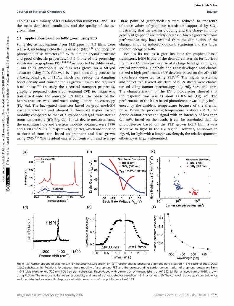
Some device applications from PLD grown h-BN films wererealized, including field-effect transistor (FET)132 and deep UVphotoconductive detectors.133 With similar crystal structureand good dielectric properties, h-BN is one of the promisingsubstrates for graphene FET.134,135 As reported by Uddin et al.,5 nm thick amorphous BN film was grown on a SiO2/Sisubstrate using PLD, followed by a post annealing process ina background gas of H2/Ar, which can reduce the danglingbond density and transfer the as-grown film to the requiredh-BN phase.132 To study the electrical transport properties,graphene prepared using a conventional CVD technique wastransferred onto the annealed BN films. The phase of theheterostructure was confirmed using Raman spectroscopy(Fig. 9a). The back-gated transistor based on graphene/h-BNwas characterized and showed a three-fold higher carriermobility compared to that of a graphene/SiO2/Si transistor atroom temperature (RT; Fig. 9b). For 35 device measurements,the maximum hole and electron mobility obtained were 4980and 4200 cm2 V�1 s�1, respectively (Fig. 9c), which are superiorto those of transistors based on graphene and h-BN grownusing CVD.134 The residual carrier concentration and average
Dirac point of graphene/h-BN were reduced to one-tenthof those values of graphene transistors supported by SiO2,illustrating that the extrinsic doping and the charge inhomo-geneity of graphene are largely decreased. Such a good electronicperformance may have resulted from the diminution of thecharged impurity induced Coulomb scattering and the largerphonon energy of h-BN.
Besides its use as a gate insulator for graphene-basedtransistors, h-BN is one of the desirable materials for fabricat-ing into a UV detector because of its large band gap and goodoptical properties. Aldalbahi and Feng developed and charac-terized a high performance UV detector based on the 2D h-BNnanosheets deposited using PLD.133 The highly crystallineand defect free layered structure of h-BN sheets were charac-terised using Raman spectroscopy (Fig. 9d), SEM and TEM.The characterization of the UV photodetector showed thatthe response time was as short as 0.6 ms (Fig. 9e). Theperformance of the h-BN-based photodetector was highly influ-enced by the ambient temperature because of the thermalnoise. When the processing temperature is above 200 1C, thedevice cannot detect the signal with an intensity of less than0.1 mW. Based on the result, it can be concluded that thephotodetector based on the PLD grown h-BN film is verysensitive to light in the UV region. However, as shown inFig. 9f, for light with a longer wavelength, the relative quantumefficiency is largely attenuated.
Fig. 9 (a) Raman spectra of graphene/h-BN heterostructure and h-BN. (b) Transfer characteristics of graphene transistors on h-BN (red line) and SiO2/Si(blue) substrates. (c) Relationship between hole mobility of a graphene FET and the corresponding carrier concentration of graphene grown on 5 nmh-BN (blue triangle) and 300 nm SiO2 (red star) substrates. Reproduced with permission of the publishers of ref. 132. (d) Raman spectrum of h-BN grownusing PLD. (e) The relationship between responsivity and time of a photodetector based on h-BN nanosheets. (f) The curve of relative quantum efficiencyand the detected wavelength. Reproduced with permission of the publishers of ref. 133.
Journal of Materials Chemistry C Review
Ope
n A
cces
s A
rtic
le. P
ublis
hed
on 3
1 A
ugus
t 201
6. D
ownl
oade
d on
02/
05/2
018
20:5
7:48
. T
his
artic
le is
lice
nsed
und
er a
Cre
ativ
e C
omm
ons
Attr
ibut
ion-
Non
Com
mer
cial
3.0
Unp
orte
d L
icen
ce.
View Article Online
8872 | J. Mater. Chem. C, 2016, 4, 8859--8878 This journal is©The Royal Society of Chemistry 2016
6. Layered GaSe nanoflakes fabricatedusing PLD
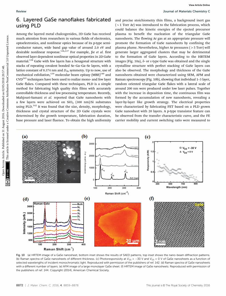
Among the layered metal chalcogenides, 2D GaSe has receivedmuch attention from researchers in various fields of electronics,optoelectronics, and nonlinear optics because of its p-type semi-conductor nature, wide band gap value of around 2.0 eV anddesirable nonlinear response.136,137 For example, Jie et al. firstobserved layer dependent nonlinear optical properties in 2D GaSematerial.138 GaSe with few layers has a hexagonal structure withstacks of repeating covalent bonded Se–Ga–Ga–Se layers, with alattice constant of 0.374 nm and D3h symmetry. Up to now, use ofmechanical exfoliation,139 molecular beam epitaxy (MBE)140 andCVD141 techniques have been used to realize mono- and few layerGaSe flakes. Compared with these techniques, PLD is a simplemethod for fabricating high quality thin films with accuratelycontrollable thickness and low processing temperature. Recently,Mahjouri-Samani et al. reported that GaSe nanosheets witha few layers were achieved on SiO2 (300 nm)/Si substratesusing PLD.142 It was found that the size, density, morphology,thickness and crystal structure of the 2D GaSe crystals weredetermined by the growth temperature, fabrication duration,base pressure and laser fluence. To obtain the high uniformity
and precise stoichiometry thin films, a background inert gas(B1 Torr Ar) was introduced to the fabrication process, whichcould balance the kinetic energies of the ejected precursorplasma to benefit the nucleation of the triangular GaSenanosheets. The flowing Ar gas at an appropriate pressure willpromote the formation of GaSe nanosheets by confining theplasma plume. Nevertheless, higher Ar pressures (45 Torr) willgenerate larger aggregated clusters that may be detrimentalto the formation of GaSe layers. According to the HRTEMimages (Fig. 10a), d- or e-type GaSe was obtained and the singlecrystalline structure with perfect stacking of GaSe layers canalso be observed. The morphology and thickness of the GaSenanosheets obtained were characterized using SEM, AFM andRaman spectroscopy (Fig. 10b), showing that individual 1–3 layer,random oriented triangular GaSe flakes with a lateral scale ofaround 200 nm were produced under low laser pulses. Togetherwith the increase in deposition time, the continuous film wasformed by the accumulation of new nanosheets, revealing alayer-by-layer like growth strategy. The electrical propertieswere characterized by fabricating FET based on a PLD grownGaSe nanosheet with 20 layers. A p-type transistor feature canbe observed from the transfer characteristic curve, and the FEcarrier mobility and current switching ratio were measured to
Fig. 10 (a) HRTEM image of a GaSe nanosheet, bottom inset shows the results of SAED patterns, top inset shows the nano-beam diffraction patterns.(b) Raman spectra of GaSe nanosheets of different thickness. (c) Photoresponsivity at VGS = �30 V and VGS = 0 V of GaSe nanosheets as a function ofselected wavelengths of incident monochromatic light. Reproduced with permission of the publishers of ref. 142. (d) Raman spectra of GaSe nanosheetswith a different number of layers. (e) AFM image of a large monolayer GaSe sheet. (f) HRTEM image of GaSe nanosheets. Reproduced with permission ofthe publishers of ref. 144. Copyright (2014), American Chemical Society.
Review Journal of Materials Chemistry C
Ope
n A
cces
s A
rtic
le. P
ublis
hed
on 3
1 A
ugus
t 201
6. D
ownl
oade
d on
02/
05/2
018
20:5
7:48
. T
his
artic
le is
lice
nsed
und
er a
Cre
ativ
e C
omm
ons
Attr
ibut
ion-
Non
Com
mer
cial
3.0
Unp
orte
d L
icen
ce.
View Article Online
This journal is©The Royal Society of Chemistry 2016 J. Mater. Chem. C, 2016, 4, 8859--8878 | 8873
be 0.1 cm2 V�1 s�1 and 104, respectively, which is comparable tothe same measurements obtained for GaSe thin sheetsobtained using mechanical exfoliation.143 The optoelectronicperformance of the GaSe-based transistor was also character-ized. The photo responsivity of the device was measured in arange of 0.4–1.4 AW�1 when illuminated with a 700 nm to240 nm light source (Fig. 10c), which is superior to theresponsivity of a phototransistor based on PLD grown WS2 thinfilms (0.51 AW�1) and comparable to that of the mechanicalexfoliated GaSe flakes.143 Based on the spectral responsivityvalue, the corresponding external quantum efficiency (EQE)can be calculated to range from 100% at 700 nm to 600% at240 nm. These high spectral responsivities are ascribed to themidgap states induced by the grain boundaries from thepolycrystallinity of the PLD grown GaSe films.
Although the stoichiometry transferred and uniform 2DGaSe nanosheets were successfully produced using PLD, theaverage small scale (B200 nm) of the obtained triangularsheets caused by the high nucleation density hinders itsreal applications. To synthesize continuous layered GaSethin films at the wafer scale, Mahjouri-Samani et al. devel-oped a new hybrid growth technique, which combinesPLD and vapor transport growth (VTG) methods, one of thepopular techniques for depositing large-scale single crystalnanosheets of layered metal chalcogenides.144 This noveltechnique has the advantages of both PLD and VTG, whichmight result in the films with accurate replication of thestoichiometry, high nucleation density, and large crystallinedomains. As the first step of this method, GaSe nanosheetswere grown using PLD on top of SiO2 (300 nm)/Si substrates,as the source substrate in this experiment. To guarantee thegood stoichiometric transfer of the thin films, a backgroundAr gas (B1 Torr) was exploited and the laser fluence was set at1 J cm�2. The morphology of the obtained GaSe film wasmainly a large amount of nanoparticles, which were detectedusing the low-resolution transmission electron microscopy(LRTEM). The second step is to attach the GaSe thin film on tothe surface of a new Si substrate, which is called the receiversubstrate, to form a confined fabrication situation. Thiscombined structure was heated up in an environment of10–20 Torr background Ar gas, resulting in a temperaturegradient for initiating growth. The growth temperature wasset to be capable of evaporating the GaSe nanoparticles ontothe receiver substrate and growth of 2D layers. A continuousmonolayer GaSe film with a typical triangular appearancewas confirmed from Raman spectroscopy (Fig. 10d) andAFM images (Fig. 10e). The maximum lateral size of thecontinuous film obtained can be up to 0.5 mm2, which ismuch larger than that of GaSe nanosheets grown usingsimple PLD. By further increasing the number of laser pulses,the individual nanosheets formed will merge into a larger andthicker continuous film as exhibited in the AFM image.Furthermore, the single crystalline, hexagonal lattice struc-ture of the GaSe film obtained was measured using HRTEMand selected area electron diffraction (SAED; Fig. 10f). ThePLD-VTG technique was also used to synthesize large-scale
monolayer MoSe2,144,145 indicating that this method is pro-mising for fabricating a variety of binary and ternary 2D metalchalcogenide thin films.
7. Black phosphorus ultrathin filmsproduced using PLD
As the most thermodynamically stable allotrope of phosphorus,BP was first synthesized from white phosphorus under highpressure in 1914.146 Similar to graphite, BP has a puckered layerstructure, with vdW interactions between adjacent layers.Although various properties of its bulk form have been inves-tigated for over 100 years, there have been only a few studies forapplying BP for useful device applications until the year of2014, and this is partially attributed to an obstacle in fabrica-tion. In 2014, Li et al. in Fudan, China and Liu et al. in Purdue,USA have done pioneer work on atomically thin BP, calledphosphorene which can be isolated by peeling it off from thebulk form.17,18 The discovery of BP has ignited the researchinterest of the scientists because of BP’s unexpected propertiescompared with its bulk counterpart.17–19 Combining the advan-tages of both graphene and MoS2, phosphorene exhibits a highcarrier mobility and a direct intrinsic band gap (0.3–2 eV),which can be tuned by the layer number. In addition, becauseof the low spin–orbit coupling, BP with few layers is alsodesirable for investigating spin transport.147
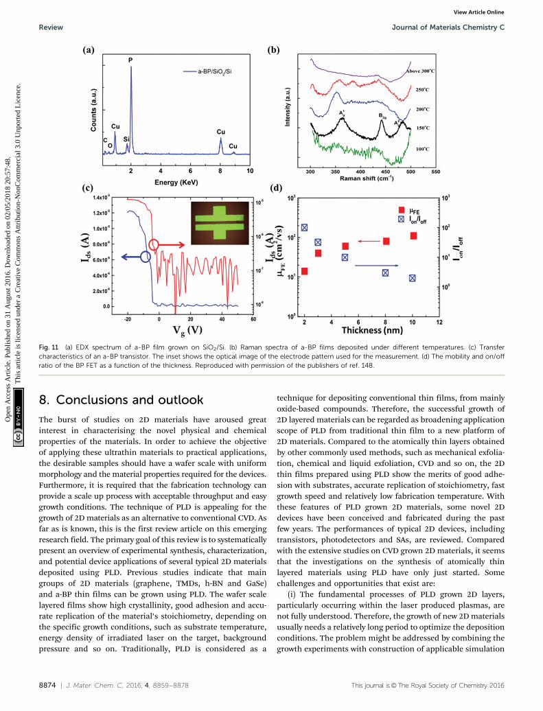
Until now, phosphorene can only be obtained by top-downmethods, namely mechanical exfoliation and solution-basedexfoliation, which only provides the small sized flakes. Becauseof the chemically active surface of ultrathin BP flakes, thechemically based bottom-up method has not yet been realizedto produce scalable BP films. Recently, PLD has been used togrow the wafer scale BP-based ultrathin films with a highlydisordered structure, called amorphous black phosphorus(a-BP), on both graphene/Cu and SiO2/Si substrates.148 Thea-BP thin films were deposited at processing temperature ofB150 1C, which is in contrast with the harsh conditionsrequired to synthesize BP bulk crystal.146 Similar to phosphor-ene, a-BP thin films show the thickness dependent direct bandgap. The chemical composition and structure were characterizedusing energy-dispersive X-ray spectroscopy (EDX) and Ramanspectroscopy (Fig. 11a and b). More importantly, the FETmeasurement shows that the as-grown a-BP thin films show ap-type behavior and high hole mobility up to 100 cm2 V�1 s�1
(Fig. 11c), which is superior to that of other commonlyused elemental amorphous semiconductor thin films, suchamorphous silicon (a-Si),149 amorphous carbon (a-C)150 oramorphous germanium (a-Ge).151 Interestingly, as shown inFig. 11d, the observed thickness dependent FE mobility andswitching ratio of the a-BP channel is similar to the perfor-mance of phosphorene-based transistors. Because the largescale film and low processing temperature are beneficial fordevice applications, it is expected that such PLD grown a-BPthin films will scientifically and technologically have moreattention in the future.
Journal of Materials Chemistry C Review
Ope
n A
cces
s A
rtic
le. P
ublis
hed
on 3
1 A
ugus
t 201
6. D
ownl
oade
d on
02/
05/2
018
20:5
7:48
. T
his
artic
le is
lice
nsed
und
er a
Cre
ativ
e C
omm
ons
Attr
ibut
ion-
Non
Com
mer
cial
3.0
Unp
orte
d L
icen
ce.
View Article Online
8874 | J. Mater. Chem. C, 2016, 4, 8859--8878 This journal is©The Royal Society of Chemistry 2016
8. Conclusions and outlook
The burst of studies on 2D materials have aroused greatinterest in characterising the novel physical and chemicalproperties of the materials. In order to achieve the objectiveof applying these ultrathin materials to practical applications,the desirable samples should have a wafer scale with uniformmorphology and the material properties required for the devices.Furthermore, it is required that the fabrication technology canprovide a scale up process with acceptable throughput and easygrowth conditions. The technique of PLD is appealing for thegrowth of 2D materials as an alternative to conventional CVD. Asfar as is known, this is the first review article on this emergingresearch field. The primary goal of this review is to systematicallypresent an overview of experimental synthesis, characterization,and potential device applications of several typical 2D materialsdeposited using PLD. Previous studies indicate that maingroups of 2D materials (graphene, TMDs, h-BN and GaSe)and a-BP thin films can be grown using PLD. The wafer scalelayered films show high crystallinity, good adhesion and accu-rate replication of the material’s stoichiometry, depending onthe specific growth conditions, such as substrate temperature,energy density of irradiated laser on the target, backgroundpressure and so on. Traditionally, PLD is considered as a
technique for depositing conventional thin films, from mainlyoxide-based compounds. Therefore, the successful growth of2D layered materials can be regarded as broadening applicationscope of PLD from traditional thin film to a new platform of2D materials. Compared to the atomically thin layers obtainedby other commonly used methods, such as mechanical exfolia-tion, chemical and liquid exfoliation, CVD and so on, the 2Dthin films prepared using PLD show the merits of good adhe-sion with substrates, accurate replication of stoichiometry, fastgrowth speed and relatively low fabrication temperature. Withthese features of PLD grown 2D materials, some novel 2Ddevices have been conceived and fabricated during the pastfew years. The performances of typical 2D devices, includingtransistors, photodetectors and SAs, are reviewed. Comparedwith the extensive studies on CVD grown 2D materials, it seemsthat the investigations on the synthesis of atomically thinlayered materials using PLD have only just started. Somechallenges and opportunities that exist are:
(i) The fundamental processes of PLD grown 2D layers,particularly occurring within the laser produced plasmas, arenot fully understood. Therefore, the growth of new 2D materialsusually needs a relatively long period to optimize the depositionconditions. The problem might be addressed by combining thegrowth experiments with construction of applicable simulation
Fig. 11 (a) EDX spectrum of a-BP film grown on SiO2/Si. (b) Raman spectra of a-BP films deposited under different temperatures. (c) Transfercharacteristics of an a-BP transistor. The inset shows the optical image of the electrode pattern used for the measurement. (d) The mobility and on/offratio of the BP FET as a function of the thickness. Reproduced with permission of the publishers of ref. 148.
Review Journal of Materials Chemistry C
Ope
n A
cces
s A
rtic
le. P
ublis
hed
on 3
1 A
ugus
t 201
6. D
ownl
oade
d on
02/
05/2
018
20:5
7:48
. T
his
artic
le is
lice
nsed
und
er a
Cre
ativ
e C
omm
ons
Attr
ibut
ion-
Non
Com
mer
cial
3.0
Unp
orte
d L
icen
ce.
View Article Online
This journal is©The Royal Society of Chemistry 2016 J. Mater. Chem. C, 2016, 4, 8859--8878 | 8875
models of PLD growth for 2D materials. Some simulations havebeen reported for the CVD growth of 2D materials.152 Unfortu-nately, there is the lack of such a model for PLD grown 2Dmaterials at this moment.
(ii) As previously introduced in the large scale GaSe fabrica-tion, the hybrid techniques combining PLD with other bottom-upmethods (CVD or MBE) can be considered to further improve thequality of the films and overcome some shortcomings of PLD,such as the thickness inhomogeneity, limited scale and poorcontinuity. This approach may provide new opportunities for PLDin the synthesis of high quality 2D materials.
(iii) Up to now, the members of the 2D material family havebeen extended to several hundred. However, the types ofmaterials already attempted to be grown using PLD are verylimited compared to the large number of members of the 2Dmaterial family. According to the literature review, some 2Dmaterials are not easy to produce using either CVD techniqueor mechanical/liquid exfoliation; examples include the chemi-cally active materials, e.g., silicene, or materials with a stronginterlayer bonding, e.g., MXenes. Obviously, it is worth explor-ing the PLD growth for more types of 2D materials.
(iv) It is feasible to implement a doping strategy during thefabrication process of PLD grown 2D materials, which has notyet been attempted. The potential methods may include eitherintermingling the dopants to the target materials, or mixing thedopants into the background gases. Therefore, it could be apromising research direction to study the doping effects on thePLD grown 2D films in the future.
Lastly, 2D vdW based heterostructures have recently showngreat promise for both fundamental study and constructing awide range of electronic and optoelectronic devices.153–156 Inthe past, PLD has proven to be a powerful tool not only indepositing a single layer of thin film, but also in in situfabricating heterostructures via sequentially rotating differenttargets without breaking the vacuum. Accordingly, it is believedthat PLD will play an important role in making various 2Dbased heterostructures for device applications in the future.
Acknowledgements
The research was supported by the grants from Research GrantsCouncil of Hong Kong (GRF No. PolyU 153031/15P), NationalNatural Science Foundation of China (Grant No. 11474241),and Collaborative Research Fund (CRF No. HKU9/CRF/13G,PolyU Grant No. E-RD5), and PolyU Internal Grant (4-BCAG).
References
1 G. E. Moore, Electronics, 1965, 38, 114.2 G. E. Moore, IEEE IEDM Tech. Dig., 1975, 21, 11.3 C. Tourney, Nat. Nanotechnol., 2016, 11, 2.4 M. M. Waldrop, Nature, 2016, 530, 144.5 S. E. Thompson and S. Parthasarathy, Mater. Today, 2006,
9, 20.6 S. Ornes, Proc. Natl. Acad. Sci. U. S. A., 2015, 112, 13128.
7 K. S. Novoselov, A. K. Geim, S. Morozov, D. Jiang, Y. Zhang,S. V. Dubonos, I. V. Grigorieva and A. A. Firsov, Science,2004, 306, 666.
8 K. Novoselov, A. Geim, S. Morozov, D. Jiang, M. Katsnelson,I. Grigorieva, S. Dubonos and A. Firsov, Nature, 2005, 438, 197.
9 D. Akinwande, P. Nicholas and H. James, Nat. Commun.,2014, 5, 5678.
10 Z. S. Butler, S. M. Hollen and L. Y. Cao, ACS Nano, 2013,7, 2898.
11 A. K. Geim and K. S. Novoselov, Nat. Mater., 2007, 6, 183.12 C. Lee, X. Wei, J. W. Kysar and J. Hone, Science, 2008,
321, 385.13 D. Sun, G. Aivazian, A. M. Jones, J. S. Ross, W. Yao,
D. Cobden and X. Xu, Nat. Nanotechnol., 2012, 7, 114.14 Q. H. Wang, K. Kalantar-Zadeh, A. Kis, J. N. Coleman and
M. S. Strano, Nat. Nanotechnol., 2012, 7, 699.15 O. N. Weiss, H. Zhou, L. Liao, Y. Liu, S. Jiang, Y. Huan and
X. Duan, Adv. Mater., 2012, 24, 5782.16 B. Radisavljevic, A. Radenovic, J. Brivio, V. Giacometti and
A. Kis, Nat. Nanotechnol., 2011, 6, 147.17 L. Li, Y. Yu, G. J. Ye, Q. Ge, X. Ou, H. Wu, D. Feng,
X. H. Chen and Y. Zhang, Nat. Nanotechnol., 2014, 9, 372.18 H. Liu, A. T. Neal, Z. Zhu, Z. Luo, X. Xu, D. Tomanek and
P. D. Ye, ACS Nano, 2014, 8, 4033.19 F. Xia, H. Wang and Y. Jia, Nat. Commun., 2014, 5, 4458.20 L. Tao, E. Cinquanta, D. Chiappe, C. Grazianetti,
M. Fanciulli, M. Dubey, A. Molle and D. Akinwande, Nat.Nanotechnol., 2015, 10, 227.
21 P. Vogt, P. D. Padava, C. Quaresima, J. Avila,E. Frantzeskakis, M. C. Asensio, A. Resta, B. Ealet andG. L. Lay, Phys. Rev. Lett., 2012, 108, 155501.
22 A. Pakdel, Y. Bando and D. Golbery, Chem. Soc. Rev., 2014,43, 934.
23 Y. Kubota, K. Watanabe, O. Tsuda and T. Taniguchi,Science, 2007, 317, 932.
24 P. Miro, M. Audiffred and T. Heine, Chem. Soc. Rev., 2014,43, 6537.
25 A. C. Ferrari, F. Bonaccorso, V. Fal’ko, K. S. Novoselov,S. Roche, P. Bøggild, S. Borini, F. H. L. Koppens, V. Palermo,N. Pugno, J. A. Garrido, R. Sordan, A. Bianco, L. Ballerini,M. Prato, E. Lidorikis, J. Kivioja, C. Marinelli, T. Ryhanen,A. Morpurgo, J. N. Coleman, V. Nicolosi, L. Colombo, A. Fert,M. Garcia-Hernandez, A. Bachtold, G. F. Schneider, F. Guinea,C. Dekker, M. Barbone, Z. Sun, C. Galiotis, A. N. Grigorenko,G. Konstantatos, A. Kis, M. Katsnelson, L. Vandersypen,A. Loiseau, V. Morandi, D. Neumaier, E. Treossi,V. Pellegrini, M. Polini, A. Tredicucci, G. M. Williams,B. H. Hong, J.-H. Ahn, J. M. Kim, H. Zirath, B. J. van Wees,H. van der Zant, L. Occhipinti, A. D. Matteo, I. A. Kinloch,T. Seyller, E. Quesnel, X. Feng, K. Teo, N. Rupesinghe,P. Hakonen, S. R. T. Neil, Q. Tannock, T. Lofwander andJ. Kinaret, Nanoscale, 2015, 7, 4598.
26 P. Avouris, Z. Chen and V. Perebeinos, Nat. Nanotechnol.,2007, 2, 605.
27 D. Xiao, G.-B. Liu, W. Feng, X. Xu and W. Yao, Phys. Rev.Lett., 2012, 108, 196802.
Journal of Materials Chemistry C Review
Ope
n A
cces
s A
rtic
le. P
ublis
hed
on 3
1 A
ugus
t 201
6. D
ownl
oade
d on
02/
05/2
018
20:5
7:48
. T
his
artic
le is
lice
nsed
und
er a
Cre
ativ
e C
omm
ons
Attr
ibut
ion-
Non
Com
mer
cial
3.0
Unp
orte
d L
icen
ce.
View Article Online
8876 | J. Mater. Chem. C, 2016, 4, 8859--8878 This journal is©The Royal Society of Chemistry 2016
28 L. Britnell, R. V. Gorbachev, R. Jalil, B. D. Belle, F. Schedin,A. Mishchenko, T. Georgiou, M. I. Katsnelson, L. Eaves,S. V. Morozov, N. M. R. Peres, J. Leist, A. K. Geim, K. S.Novoselov and L. A. Ponomarenko, Science, 2012, 335, 947.
29 Y. Shi, H. Li and L.-J. Li, Chem. Soc. Rev., 2015, 44, 2744.30 Q. Ji, Y. Zhang, Y. Zhang and Z. Liu, Chem. Soc. Rev., 2015,
44, 2587.31 C. Mattevi, H. Kim and M. Chhowalla, J. Mater. Chem.,
2011, 21, 3324.32 H. F. Liu, S. L. Wong and D. Z. Chi, Chem. Vap. Deposition,
2015, 21, 241.33 B. Roas, L. Schultz and G. Endres, Appl. Phys. Lett., 1988,
53, 1557.34 J. H. Hao, Y. Zhang and X. H. Wei, Angew. Chem., 2011,
123, 7008.35 I. A. Akimov, A. A. Sirenko, A. M. Clark, J. H. Hao and
X. X. Xi, Phys. Rev. Lett., 2000, 84, 4625.36 G. X. Bai, Y. Zhang and J. H. Hao, Sci. Rep., 2014, 4, 5724.37 Y. Zhang and J. H. Hao, J. Appl. Phys., 2013, 113, 184112.38 Z. B. Yang and J. H. Hao, J. Appl. Phys., 2012, 112, 054110.39 Y. Zhang, G. Y. Gao, H. L. W. Chan, J. Y. Dai, Y. Wang and
J. H. Hao, Adv. Mater., 2012, 24, 1729.40 J. H. Hao, W. D. Si, X. X. Xi, R. Guo, A. S. Bhalla and
L. E. Cross, Appl. Phys. Lett., 2000, 76, 3100.41 Z. B. Yang, W. Huang and J. H. Hao, Appl. Phys. Lett., 2013,
103, 031919.42 W. Huang, J. Y. Dai and J. H. Hao, Appl. Phys. Lett., 2010,
97, 162905.43 W. Huang, Z. P. Wu and J. H. Hao, Appl. Phys. Lett., 2009,
94, 032905.44 J. H. Hao, J. Gao, Z. Wang and D. P. Yu, Appl. Phys. Lett.,
2005, 87, 131908.45 K. Nomura, H. Ohta, A. Takagi, T. Kamiya, M. Hirano and
H. Hosono, Nature, 2004, 432, 488.46 W. Hoheisel, K. Jungmann, M. Vollmer, R. Weidenauer
and F. Trager, Phys. Rev. Lett., 1988, 60, 1649.47 D. J. Krajnovich, J. E. Vazquez and R. J. Savoy, Science,
1993, 259, 1590.48 S. Amoruso, G. Ausanio, C. de Lisio, V. Iannotti, M. Vitiello,
X. Wang and L. Lanotte, Appl. Surf. Sci., 2005, 247, 71.49 B. Holzapfel, B. Roas, L. Schultz, P. Bauer and G. Saemann-
Ischenko, Appl. Phys. Lett., 1992, 61, 3178.50 Z. Trajanovic, S. Choopun, R. P. Sharma and
T. Venkatesan, Appl. Phys. Lett., 1997, 70, 3461.51 H. L. Spindler, R. M. Gilgenbach and J. S. Lash, Appl. Phys.
Lett., 1996, 68, 3245.52 Z. Liu, S. P. Lau and F. Yan, Chem. Soc. Rev., 2015, 44, 5638.53 H. Zeng, J. Dai, W. Yao, D. Xiao and X. Cui, Nat. Nano-
technol., 2012, 7, 490.54 M. Buscema, D. J. Groenendijk, G. A. Steele, H. S. J. van der
Zant and A. Castellanos-Gomez, Nat. Commun., 2014,5, 4651.
55 C. Lee, H. Yan, L. E. Brus, T. F. Heinz, J. Hone and S. Ryu,ACS Nano, 2010, 4, 2695.
56 L. J. Cote, F. Kim and J. Huang, J. Am. Chem. Soc., 2008,131, 1043.
57 M. Chhowalla, H. S. Shin, G. Eda, L.-J. Li, K. P. Loh andH. Zhang, Nat. Chem., 2013, 5, 263.
58 L. Tang, R. Ji, X. Li, G. Bai, C. P. Liu, J. Hao, J. Lin, H. Jiang,K. S. Teng, Z. Yang and S. P. Lau, ACS Nano, 2014, 8, 6312.
59 S. Lin, S. Liu, Z. Yang, Y. Li, T. W. Ng, Z. Xu, Q. Bao, J. Hao,C.-S. Lee, C. Surya, F. Yan and S. P. Lau, Adv. Funct. Mater.,2016, 26, 864.
60 G. Bai, S. Yuan, Y. Zhao, Z. Yang, S. Y. Choi, Y. Chai,S. F. Yu, S. P. Lau and J. Hao, Adv. Mater., 2016, 28, 7472.
61 W. Jie, F. Zheng and J. Hao, Appl. Phys. Lett., 2013,103, 233111.
62 J. Deng, R. Zheng, Y. Zhao and G. Cheng, ACS Nano, 2012,6, 3727.
63 C. Gong, C. Huang, J. Miller, L. Cheng, Y. Hao, D. Cobden,J. Kim, R. S. Ruoff, R. M. Wallace, K. Cho, X. Xu andY. J. Chabal, ACS Nano, 2013, 7, 11350.
64 Q. Feng, Y. Zhu, J. Hong, M. Zhang, W. Duan, N. Mao,J. Wu, H. Xu, F. Dong, F. Lin, C. Jin, C. Wang, J. Zhang andL. Xie, Adv. Mater., 2014, 26, 2648.
65 E. Cappelli, S. Lacobucci, C. Scilletta, R. Flammini,S. Orlando, G. Mattei, P. Ascarelli, F. Borgatti, A. Giglia,N. Mahne and S. Nannarone, Diamond Relat. Mater., 2005,14, 959.
66 C. Scilletta, M. Servidori, S. Orlando, E. Cappelli, L. Barbaand P. Ascarelli, Appl. Surf. Sci., 2006, 252, 4877.
67 E. Cappelli, S. Orlando, M. Servidori and C. Scilletta, Appl.Surf. Sci., 2007, 254, 1273.
68 J. Coraux, A. T. N’diaye, C. Busse and T. Michely, NanoLett., 2008, 8, 565.
69 A. T. T. Koh, Y. M. Foong and D. H. C. Chua, Appl. Phys.Lett., 2010, 97, 114102.
70 K. Wang, G. Tai, K. H. Wong, S. P. Lau and W. Guo, AIPAdv., 2011, 1, 022141.
71 A. T. T. Koh, Y. M. Foong and D. H. C. Chua, DiamondRelat. Mater., 2012, 25, 98.
72 G. K. Hemani, W. G. Vandenberghe, B. Brennan,Y. J. Chabal, A. V. Walker, R. M. Wallace, M. Quevedo-Lopez and M. V. Fischetti, Appl. Phys. Lett., 2013,103, 134102.
73 V. Kaushik, H. Sharma, A. K. Shukla and V. D. Vankar,Vacuum, 2014, 110, 1.
74 J. Wang, Z. Xiong, J. Yu, H. Yin, X. Wang, L. Peng, Y. Wang,X. Wang, T. Jiang, L. Cao, W. Wu, C. Wang and L. Zhang,Micro Nano Lett., 2015, 10, 649.
75 P. Fortgang, T. Tite, V. Barnier, N. Zehani, C. Maddi,F. Lagarde, A.-S. Loir, N. Jaffrezic-Renault, C. Donnet,F. Garrelie and C. Chaix, ACS Appl. Mater. Interfaces,2016, 8, 1424.
76 M. Qian, Y. S. Zhou, Y. Gao, J. B. Park, T. Feng,S. M. Huang, Z. Sun, L. Jiang and Y. F. Lu, Appl. Phys.Lett., 2011, 98, 173108.
77 M. Reininghaus, D. Wortmann, J. Finger, O. Faley,R. Poprawe and C. Stampfer, Appl. Phys. Lett., 2012,100, 151606.
78 S. R. Sarath Kumar and H. N. Alshareef, Appl. Phys. Lett.,2013, 102, 012110.
Review Journal of Materials Chemistry C
Ope
n A
cces
s A
rtic
le. P
ublis
hed
on 3
1 A
ugus
t 201
6. D
ownl
oade
d on
02/
05/2
018
20:5
7:48
. T
his
artic
le is
lice
nsed
und
er a
Cre
ativ
e C
omm
ons
Attr
ibut
ion-
Non
Com
mer
cial
3.0
Unp
orte
d L
icen
ce.
View Article Online
This journal is©The Royal Society of Chemistry 2016 J. Mater. Chem. C, 2016, 4, 8859--8878 | 8877
79 I. Kumar and A. Khare, Appl. Surf. Sci., 2014, 317, 1004.80 S. C. Xu, B. Y. Man, S. Z. Jiang, A. H. Liu, G. D. Hu,
C. S. Chen, M. Liu, C. Yang, D. J. Feng and C. Zhang, LaserPhys. Lett., 2014, 11, 096001.
81 X. Dong, S. Liu, H. Song, P. Gu and X. Li, Chin. Opt. Lett.,2015, 13, 021601.
82 B. J. Na, T. H. Kim, C. Lee and S. H. Lee, Tran. Electr.Electron. Mater., 2015, 16, 70.
83 E. Kymakis, K. Savva, M. M. Stylianakis, C. Fotakis andE. Stratakis, Adv. Funct. Mater., 2013, 23, 2742.
84 S. R. Sarath Kumar, P. K. Nayak, M. N. Hedhili, M. A. Khanand H. N. Alshareef, Appl. Phys. Lett., 2013, 103, 192109.
85 A. Fattah and S. Khatami, Opt. Quantum Electron., 2015,47, 613.
86 S. M. Maliyekkal, T. S. Sreeprasad, D. Krishnan, S. Kouser,A. K. Mishra, U. V. Waghmare and T. Pradeep, Small, 2013,9, 273.
87 T. Tite, C. Donnet, A.-S. Loir, S. Reynaud, J.-Y. Michalon,F. Vocanson and F. Garrelie, Appl. Phys. Lett., 2014,104, 041912.
88 M. S. Donley, P. T. Murray, S. A. Barber and T. W. Haas,Surf. Coat. Technol., 1988, 36, 329.
89 S. D. Walek, M. S. Donley, J. S. Zabinski and V. J. Dyhouse,J. Mater. Res., 1993, 8, 2933.
90 S. D. Walck, J. S. Zabinski and M. S. Donley, Surf. Coat.Technol., 1993, 62, 412.
91 N. T. McDevitt, J. S. Zabinski and M. S. Donley, Thin SolidFilms, 1994, 240, 76.
92 T. A. J. Loh and D. H. C. Chua, ACS Appl. Mater. Interfaces,2014, 6, 15966.
93 T. A. J. Loh and D. H. C. Chua, Chem. Phys. Lett., 2014,610, 284.
94 C. R. Serrao, A. M. Diamond, S. L. Hsu, L. You, S. Gadgil,J. Clarkson, C. Carraro, R. Maboudian, C. Hu andS. Salahuddin, Appl. Phys. Lett., 2015, 106, 052101.
95 Y. T. Ho, C.-H. Ma, T.-T. Luong, L.-L. Wei, T.-C. Yen,W.-T. Hsu, W.-H. Chang, Y.-C. Chu, Y.-Y. Tu, K. P. Pandeand E. Y. Chang, Phys. Status Solidi RRL, 2015, 9, 187.
96 S. Siegel, Y. P. Venkata Subbaiah, M. C. Prestgard andA. Tiwari, APL Mater., 2015, 3, 056103.
97 S. Wang, H. Yu, H. Zhuang, A. Wang, M. Zhao, Y. Chen,L. Mei and J. Wang, Adv. Mater., 2014, 26, 3538.
98 R. I. Woodward, R. C. T. Howe, G. Hu, F. Torrisi, M. Zhang,T. Hasan and E. J. R. Kelleher, Photonics Res., 2015, 3, 30.
99 Y. Zhang, S. Wang, H. Yu, H. Zhang, Y. Chen, L. Mei,A. D. Lieto, M. Tonelli and J. Wang, Sci. Rep., 2015,5, 11342.
100 Y. Zhang, S. Wang, D. Wang, H. Yu, H. Zhang, Y. Chen,L. Mei, A. D. Lieto, M. Tonelli and J. Wang, IEEE PhotonicsTechnol. Lett., 2015, 28, 197.
101 M. I. Serna, S. H. Yoo, S. Moreno, Y. Xi, J. P. Oviedo,H. Choi, H. N. Alshareef, M. J. Kim, M. Minary-Jolandanand M. A. Quevedo-Lopez, ACS Nano, 2016, 10, 6054.
102 D. J. Late, P. A. Shaikh, R. Khare, R. V. Kashid,M. Chaudhary, M. A. More and S. B. Ogale, ACS Appl.Mater. Interfaces, 2014, 6, 15881.
103 R. V. Kashid, D. J. Late, S. S. Chou, Y. K. Huang, M. De,D. S. Joag, M. A. More and V. P. Dravid, Small, 2013,9, 2730.
104 Q. L. Bao, H. Zhang, Y. Wang, Z. H. Ni, Y. L. Yan,Z. X. Shen, K. P. Loh and D. Y. Tang, Adv. Funct. Mater.,2009, 19, 3077.
105 Z. Sun, T. Hasan, F. Torrisi, D. Popa, G. Privitera, F. Wang,F. Bonaccorso, D. M. Basko and A. C. Ferrari, ACS Nano,2010, 4, 803.
106 S. N. Grigoriev, V. Y. Fominski, R. I. Romanov, A. G.Gnedovets and M. A. Volosova, Appl. Surf. Sci., 2013, 282, 607.
107 T. A. J. Loh, D. H. C. Chua and A. T. S. Wee, Sci. Rep., 2015,5, 18116.
108 T. A. J. Loh and D. H. C. Chua, J. Phys. Chem. C, 2015,119, 27496.
109 M. Schenato, C. L. A. Ricardo, P. Scardi, R. Edla,A. Miotello, M. Orlandi and R. Morrish, Appl. Catal., A,2016, 510, 156.
110 J. D. Yao, Z. Q. Zheng, J. M. Shao and G. W. Yang,Nanoscale, 2015, 7, 14974.
111 P. Yan, A. Liu, Y. Chen, H. Chen, S. Ruan, C. Guo, S. Chen,I. L. Li, H. Yang, J. Hu and G. Cao, Opt. Mater. Express,2015, 5, 479.
112 B. Guo, Y. Yao, P. G. Yan, K. Xu, J.-J. Liu, S.-G. Wang andY. Li, IEEE Photonics Technol. Lett., 2016, 28, 323.
113 Y.-H. Lee, L. Yu, H. Wang, W. Fang, X. Ling, Y. Shi,C.-T. Lin, J.-K. Huang, M.-T. Chang, C.-S. Chang,M. Dresselhaus, T. Palacios, L.-J. Li and J. Kong, NanoLett., 2013, 13, 1852.
114 H. Zhang, S. B. Lu, J. Zheng, J. Du, S. C. Wen, D. Y. Tangand K. P. Loh, Opt. Express, 2014, 22, 7249.
115 R. T. Paine and C. K. Narula, Chem. Rev., 1990, 90, 73.116 L. Song, L. Ci, H. Lu, P. B. Sorokin, C. Jin, J. Ni,
A. G. Kvashnin, D. G. Kvashnin, J. Lou, B. I. Yakobsonand P. M. Ajayan, Nano Lett., 2010, 10, 3209.
117 J. Xue, J. Sanchez-Yamagishi, D. Bulmash, P. Jacquod,A. Deshpande, K. Watanabe, T. Taniguchi, P. Jarillo-Herreroand B. J. LeRoy, Nat. Mater., 2011, 10, 282.
118 R. B. Kaner, J. Kouvetakis, C. E. Warble, M. L. Sattler andN. Bartlett, Mater. Res. Bull., 1987, 22, 399.
119 G. Reisse and S. Weissmantel, Appl. Phys. A: Mater. Sci.Process., 1999, 69, 749.
120 P. X. Feng and M. Sajjad, Mater. Lett., 2012, 89, 206.121 M. Sajjad, G. Morell and P. Feng, ACS Appl. Mater. Inter-
faces, 2013, 5, 5051.122 M. Sajjad, M. Ahmadi, M. J.-F. Guinel, Y. Lin and P. Feng,
J. Mater. Sci., 2013, 48, 2543.123 A. Aldalbahi, A. F. Zhou and P. Feng, Sci. Rep., 2015,
5, 16703.124 P. Feng, M. Sajjad, E. Y. Li, H. Zhang, J. Chu, A. Aldalbahi
and G. Morell, Beilstein J. Nanotechnol., 2014, 5, 1186.125 M. Sajjad, H. X. Zhang, X. Y. Peng and P. X. Feng, Phys. Scr.,
2011, 83, 065601.126 M. Sajjad and P. Feng, Appl. Phys. Lett., 2011, 99, 253109.127 M. Sajjad, X. Peng, J. Chu, H. Zhang and P. Feng, J. Mater.
Res., 2013, 28, 1747.
Journal of Materials Chemistry C Review
Ope
n A
cces
s A
rtic
le. P
ublis
hed
on 3
1 A
ugus
t 201
6. D
ownl
oade
d on
02/
05/2
018
20:5
7:48
. T
his
artic
le is
lice
nsed
und
er a
Cre
ativ
e C
omm
ons
Attr
ibut
ion-
Non
Com
mer
cial
3.0
Unp
orte
d L
icen
ce.
View Article Online
8878 | J. Mater. Chem. C, 2016, 4, 8859--8878 This journal is©The Royal Society of Chemistry 2016
128 P. Feng, E. Y. Li, M. Sajjad, A. Aldalbahi and J. Chu, Sci.Adv. Mater., 2015, 7, 1326.
129 N. R. Glavin, M. L. Jespersen, M. H. Check, J. Hu,A. M. Hilton, T. S. Fisher and A. A. Voevodin, Thin SolidFilms, 2014, 572, 245.
130 N. R. Glavin, C. Muratore, M. L. Jespersen, J. Hu, T. S. Fisherand A. A. Voevodin, J. Appl. Phys., 2015, 117, 165305.
131 D. Velazquez, R. Seiber, H. Man, L. Spentzouris andJ. Terry, J. Appl. Phys., 2016, 119, 095306.
132 M. A. Uddin, N. Glavin, A. Singh, R. Naguy, M. Jespersen,A. Voevodin and G. Koley, Appl. Phys. Lett., 2015, 107, 203110.
133 A. Aldalbahi and P. Feng, IEEE Trans. Electron Devices,2015, 62, 1885.
134 C. R. Dean, A. F. Young, I. Meric, C. Lee, L. Wang,S. Sorgenfrei, K. Watanabe, T. Taniguchi, P. Kim andK. L. Shepard, Nat. Nanotechnol., 2010, 5, 722.
135 L. Wang, B. Wu, J. Chen, H. Liu, P. Hu and Y. Liu, Adv.Mater., 2014, 26, 1559.
136 D. J. Late, B. Liu, J. Luo, A. Yan, H. S. S. RamakrishnaMatte, M. Grayson, C. N. R. Rao and V. P. Dravid, Adv.Mater., 2012, 24, 3549.
137 Y. Zhou, Y. Nie, Y. Liu, K. Yan, J. Hong, C. Jin, Y. Zhou,J. Yin, Z. Liu and H. Peng, ACS Nano, 2014, 8, 1485.
138 W. Jie, X. Chen, D. Li, L. Xie, Y. Y. Hui, S. P. Lau, X. Cui andJ. H. Hao, Angew. Chem., Int. Ed., 2015, 54, 1185.
139 L. Karvonen, A. Saynatjoki, S. Mehravar, R. D. Rodriguez,S. Hartmann, D. R. T. Zahn, S. Honkanen, R. A. Norwood,N. Peyghambarian, K. Kieu, H. Lipsanen and J. Riikonen,Sci. Rep., 2015, 5, 10334.
140 X. Yuan, L. Tang, S. Liu, P. Wang, Z. Chen, C. Zhang,Y. Liu, W. Wang, Y. Zou, C. Liu, N. Guo, J. Zou, P. Zhou,W. Hu and F. Xiu, Nano Lett., 2015, 15, 3571.
141 M. A. Malik, M. Afzaal and P. O’Brien, Chem. Rev., 2010,110, 4417.
142 M. Mahjouri-Samani, R. Gresback, M. K. Tian, K. Wang,A. A. Puretzky, C. M. Rouleau, G. Eres, I. N. Ivanov, K. Xiao,
M. A. McGuire, G. Duscher and D. B. Geohegan, Adv. Funct.Mater., 2014, 24, 6365.
143 P. A. Hu, Z. Wen, L. Wang and K. Xiao, ACS Nano, 2012,6, 5988.
144 M. Mahjouri-Samani, M. Tian, K. Wang, A. Boulesbaa,C. M. Rouleau, A. A. Puretzky, M. A. McGuire, B. R.Srijanto, K. Xiao, G. Eres, G. Duscher and D. B. Geohegan,ACS Nano, 2014, 8, 11567.
145 A. A. Puretzky, L. Liang, X. Li, K. Xiao, K. Wang,M. Mahjouri-Samani, L. Basile, J. C. Idrobo, B. G. Sumpter,V. Meunier and D. B. Geohegan, ACS Nano, 2015, 9, 6333.
146 H. Liu, Y. Du, Y. Deng and P. D. Ye, Chem. Soc. Rev., 2015,9, 2732.
147 A. S. Robin, A. Carvalho and A. H. Castro Neto, Phys. Rev.Lett., 2014, 112, 176801.
148 Z. B. Yang, J. H. Hao, S. G. Yuan, S. H. Lin, H. M. Yau,J. Y. Dai and S. P. Lau, Adv. Mater., 2015, 27, 3748.
149 E. Fortunato, P. Barquinha and R. Matins, Adv. Mater.,2012, 24, 2945.
150 R. U. R. Sagar, X. Z. Zhang, C. Y. Xiong and Y. Yu, Carbon,2014, 76, 64.
151 P. Yan, N. N. Lichtin and D. L. Morel, Appl. Phys. Lett.,1987, 50, 1367.
152 H. Shu, X. Chen, X. Tao and F. Ding, ACS Nano, 2012,6, 3243.
153 W. Jie and J. H. Hao, Nanoscale, 2014, 6, 6346.154 C. Huang, S. Wu, A. M. Sanchez, J. J. Peters, R. Beanland,
J. S. Ross, P. Rivera, W. Yao, D. H. Cobden and X. Xu, Nat.Mater., 2014, 13, 1096.
155 J. S. Ross, P. Klement, A. M. Jones, N. J. Ghimire, J. Yan,D. G. Mandrus, T. Taniguchi, K. Watanabe, K. Kitamura,W. Yao, D. H. Cobden and X. Xu, Nat. Nanotechnol., 2014,9, 268.
156 W. Pan, J. Xiao, J. Zhu, C. Yu, G. Zhang, Z. Ni, K. Watanabe,T. Taniguchi, Y. Shi and X. Wang, Sci. Rep., 2012,2, 893.
Review Journal of Materials Chemistry C
Ope
n A
cces
s A
rtic
le. P
ublis
hed
on 3
1 A
ugus
t 201
6. D
ownl
oade
d on
02/
05/2
018
20:5
7:48
. T
his
artic
le is
lice
nsed
und
er a
Cre
ativ
e C
omm
ons
Attr
ibut
ion-
Non
Com
mer
cial
3.0
Unp
orte
d L
icen
ce.
View Article Online
Related Documents