bulletin emerging ceramics & glass technology AMERICAN CERAMIC SOCIETY APRIL 2022 Structured glass for semiconductors | Next-generation memory | AGG celebrates IYOG Progress and future prospects of negative capacitance electronics: A materials perspective POLICY RECOMMENDATIONS: US MUST LEAD IN BUILDING THE WESTERN SUPPLY CHAIN THE RARE EARTHS ECONOMY: CAN SUPPLY KEEP UP WITH GROWING DEMAND? www.ceramics.org/ceramicandglassmanufacturing APRIL 2022 • VOLUME 3 • ISSUE 1 Shredding discarded hard drives at the Critical Materials Institute at Ames Laboratory. New issue inside:

Welcome message from author
This document is posted to help you gain knowledge. Please leave a comment to let me know what you think about it! Share it to your friends and learn new things together.
Transcript

bulletine m e r g i n g c e r a m i c s & g l a s s t e c h n o l o g y
A M E R I C A N C E R A M I C S O C I E T Y
APRIL 2022
Structured glass for semiconductors | Next-generation memory | AGG celebrates IYOG
Progress and future prospects of negative capacitance electronics: A materials perspective
P O L I C Y R E C O M M E N D A T I O N S : U S M U S T L E A D I N B U I L D I N G T H E W E S T E R N S U P P L Y C H A I N
THE RARE EARTHS ECONOMY: CAN SUPPLY KEEP UP WITH GROWING DEMAND?
www.ceramics.org/ceramicandglassmanufacturing
A P R I L 2 0 2 2 • V O L U M E 3 • I S S U E 1
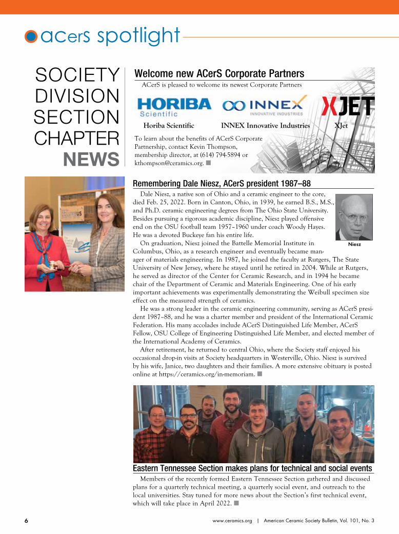
Shredding discarded hard drives at the Critical Materials Institute at Ames Laboratory.
New issue inside:

www.harropusa.com1.614.231.3621
When it Comes to Heat, We Sweat the Details!
Our laboratory can run tests to help identify your process boundaries. Through our toll firing facility, we can
help to further define the equipment/
processing combination that
works best for your material. And if you
are not ready for a new kiln, we can toll fire your material to
help meet your production needs.
Does your current kiln company
sweat the details?
Your firing needs are unique. So why use an “off the shelf” kiln in your process?
At Harrop, we get it. That’s why, for over a century, we’ve been putting in the hard work to design and service custom kilns. Is it harder to do things this way? Yes. Is the extra effort worth it? You bet!
At Harrop, we don’t stop there. If you aren’t sure what you need, we can help.
Harrop Ad Sweat the Details ACerS Full Size w 100 logo.indd 1Harrop Ad Sweat the Details ACerS Full Size w 100 logo.indd 1 5/21/20 9:33 AM5/21/20 9:33 AM

American Ceramic Society Bulletin, Vol. 101, No. 3 | www.ceramics.org 1
Volume 3, Issue 1 — Ceramic & Glass ManufacturingThe rare earths economy: Can supply keep up with growing demand?
Also inside:• Industry news• Policy recommendations: US must lead in
building the Western supply chain
Editor’s note:Attentive readers may notice that this Bulletin is more slender than usual. A normal Bulletin and C&GM combined issue would run 64 pages, but an acute, global shortage of the paper we use forced us to reduce the number of pages printed. After careful consideration, we opted to print less content rather than publish a magazine with content split between print and online. The paper shortage is expected to continue through spring 2022. For more information on the short-age, visit our website at www.ceramics.org or contact customer service at [email protected].
Correction:The March 2022 issue of the Bulletin featured the incorrect logo for our new Corporate Partner Carborundum Universal Ltd. Included here are the correct logos.
Progress and future prospects of negative capacitance electronics: A materials perspectiveAs miniaturization reaches its limits to improve the effi-ciency of transistors, researchers are exploring the possi-bility of using ferroelectric materials to boost performance through negative capacitance behavior. Includes an intro-duction by coauthor Michael Hoffmann.
by Michael Hoffmann, Stefan Slesazeck, and Thomas Mikolajickk
22
Structured glass: A new frontier for semiconductorsUltrafine structured glass offers a game-changing ele-ment to semiconductor packaging. SCHOTT recently introduced FLEXINITY® connect, their ultrafine struc-tured glass solution.
by Tobias Gotschke
departmentNews & Trends . . . . . . . . . . . . . . . 2
Spotlight . . . . . . . . . . . . . . . . . . . . . 6
Ceramics in the Environment . . 14
Ceramics in Manufacturing . . . . 16
Ceramics in Biomedicine . . . . . . 17
Research Briefs . . . . . . . . . . . . . . 18
columnsInternational Year of Glass . . . . . 5The American Glass Guild unites artists and scholars of stained glass
By Kathy Jordan
Business and Market View . . . . 13Next-generation memory: Global markets to 2026
By BCC Publishing Staff
Deciphering the Discipline . . . . . 48Emerging materials for semiconductors: Oxides for stable solar fuel productionBy Jake Evans
meetingsUpcoming dates: . . . . . . . . . . . . . 31 GOMD, Cements, PACC-FMAs, and MS&T annual meeting
resourcesCalendar . . . . . . . . . . . . . . . . . . . . 32Classified Advertising . . . . . . . . . 45Display Ad Index . . . . . . . . . . . . . 47
feature articles
30
contentsA p r i l 2 0 2 2 • V o l . 1 0 1 N o . 3
cove
r st
ory
P O L I C Y R E C O M M E N D A T I O N S : U S M U S T L E A D
I N B U I L D I N G T H E W E S T E R N S U P P L Y C H A I N THE RARE EARTHS ECONOMY:
CAN SUPPLY KEEP UP WITH GROWING DEMAND?
www.ceramics.org/ceramicandglassmanufacturing
A P R I L 2 0 2 2 • V O L U M E 3 • I S S U E 1
Shredding discarded hard drives at the Critical
Materials Institute at Ames Laboratory.
33

www.ceramics.org | American Ceramic Society Bulletin, Vol. 101, No. 32
bulletinAMERICAN CERAMIC SOCIETY
American Ceramic Society Bulletin covers news and activities of the Society and its members, includes items of interest to the ceramics community, and provides the most current information concerning all aspects of ceramic technology, including R&D, manufacturing, engineering, and marketing. The American Ceramic Society is not responsible for the accuracy of information in the editorial, articles, and advertising sections of this publication. Readers should independently evaluate the accuracy of any statement in the editorial, articles, and advertising sections of this publication. American Ceramic Society Bulletin (ISSN No. 0002-7812). ©2022. Printed in the United States of America. ACerS Bulletin is published monthly, except for February, July, and November, as a “dual-media” magazine in print and electronic formats (www.ceramics.org). Editorial and Subscription Offices: 550 Polaris Parkway, Suite 510, Westerville, OH 43082-7045. Subscription included with The American Ceramic Society membership. Nonmember print subscription rates, including online access: United States and Canada, 1 year $135; international, 1 year $150.* Rates include shipping charges. International Remail Service is standard outside of the United States and Canada. *International nonmembers also may elect to receive an electronic-only, email delivery subscription for $100. Single issues, January–October/November: member $6 per issue; nonmember $15 per issue. December issue (ceramicSOURCE): member $20, nonmember $40. Postage/handling for single issues: United States and Canada, $3 per item; United States and Canada Expedited (UPS 2nd day air), $8 per item; International Standard, $6 per item.
POSTMASTER: Please send address changes to American Ceramic Society Bulletin, 550 Polaris Parkway, Suite 510, Westerville, OH 43082-7045. Periodical postage paid at Westerville, Ohio, and additional mailing offices. Allow six weeks for address changes.
ACSBA7, Vol. 101, No. 3, pp 1– 48. All feature articles are covered in Current Contents.
Editorial and ProductionEileen De Guire, Editor [email protected] McDonald, Associate Managing EditorMichelle Martin, Production EditorTess Speakman, Senior Graphic Designer
Editorial Advisory BoardScott Cooper, Owens-IllinoisYakup Gönüllü, Schott AGMichael Hill, TevTech Inc.Eliana Muccillo, IPEN-SP, BrazilOomman Varghese, University of HoustonKelley Wilkerson, Missouri S&T
Customer Service/Circulation ph: 866-721-3322 fx: 240-396-5637 [email protected]
Advertising SalesNational SalesKevin Thompson, Industry Relations Director [email protected] ph: 614-794-5894
EuropeRichard Rozelaar [email protected] ph: 44-(0)-20-7834-7676 fx: 44-(0)-20-7973-0076
Executive Staff Mark Mecklenborg, Executive Director and Publisher [email protected] De Guire, Director of Technical Publications and Communications [email protected] Marcus Fish, Development DirectorCeramic and Glass Industry Foundation [email protected] Michael Johnson, Director of Finance and Operations [email protected] Kibble, Director of Information Technology [email protected] LaBute, Executive Office Manager [email protected] Ross, Director of Meetings, Membership and Marketing [email protected] Thompson, Industry Relations Director [email protected]
OfficersElizabeth Dickey, PresidentSanjay Mathur, President-electDana Goski, Past PresidentStephen Houseman, TreasurerDaniel Tipsord, Treasurer-electMark Mecklenborg, Secretary
Board of Directors Helen Chan, Director 2019–2022Monica Ferraris, Director 2019–2022 William Headrick, Director 2019–2022Darryl Butt, Director 2020–2023 Eva Hemmer, Director 2020–2023Makio Naito, Director 2020–2023 Kristin Breder, Director 2021–2024 Olivia Graeve, Director 2021–2024 Shibin Jiang, Director 2021–2024 Stephen Freiman, Parliamentarian
news & trends
US electric vehicle charging infrastructure poised for major expansion
On Nov. 15, 2021, President Biden signed the Infrastructure Investment and Jobs Act into law. Among its many initiatives, this bipartisan law estab-lished the National Electric Vehicle Infrastructure (NEVI) Formula Program, which aims “to provide funding to States to strategically deploy electric vehicle (EV) charging infrastructure and to establish an interconnected network to facilitate data collection, access, and reli-ability,” according to a Department of Transportation fact sheet.
On Feb. 10, 2022, the U.S. Departments of Transportation and Energy announced they will begin making available the nearly $5 billion included in the infrastructure law for the NEVI Formula Program. The fund-ing, which will be distributed over the next five years, will be used to create a network of EV charging stations along designated Alternative Fuel Corridors, which are a national network for alterna-tive fueling and electric vehicle charging infrastructure along national highway system corridors.
“Americans need to know that they can purchase an electric vehicle and find convenient charging stations when they are using Interstates and other major highways,” says Deputy Federal Highway Administrator Stephanie Pollack in a Department of Transportation press release. “The new EV formula program will provide states with the resources they need to provide their residents with
reliable access to an EV charging station as they travel.”
To access the NEVI funds, each state is required to submit an EV Infrastructure Deployment Plan to the new Joint Office of Energy and Transportation that describes how the state intends to use its share of the funds consistent with Federal Highway Administration guidance.
The Department of Transportation also released a new, free resource to help rural communities take full advantage of the funds at https://www.transportation.gov/rural/ev/toolkit.
An Insider article on the announce-ment elaborates some more details of the plan, including that a state can apply for funding to place charging stations in other public places such as transit sta-tions, schools, and parking lots once its corridors are “fully built out.” A corridor will be considered built out once it has a series of charging stations no more than 50 miles apart along Interstate highways, with each station featuring at least four DC fast charging plugs capable of pro-
Cre
dit:
Tom
my
Kro
mb
ache
r, U
nsp
lash

American Ceramic Society Bulletin, Vol. 101, No. 3 | www.ceramics.org 3
news & trends
viding 150 kilowatts of energy each.Market analysts note that this funding
is only a small first step toward reach-ing the Biden Administration’s goal of 500,000 public EV chargers by 2030 (the U.S. currently has just over 100,000).
As a Grist article explains, “According to the International Council on Clean Transportation, it costs between $30,000 and $140,000 to install a single DC fast charger. That means that the cash allo-cated could pay for between 36,000 and 166,000 fast chargers across the coun-try—although it could be much more if states and private companies contribute their own funds, too.”
However, U.S. Secretary of Transportation Pete Buttigieg is confident that EV charging will be increasingly cost-effective even without government support. “The fuel savings of electric compared to gas or diesel continue to bear out,” he says in the Grist article. “We just haven’t yet seen the market mature.” n
Vessel shortage could hamper offshore wind expansion
When faced with the energy crisis of the 1970s, key United States govern-ment personnel and agencies projected that the sun’s “huge and virtually inex-haustible potential supply of energy” would likely serve as a mainstay of the energy industry in the future. Fifty years later, it is instead wind energy that has come to play a significant role, account-ing for about 8% of U.S. electricity generation in 2020 in contrast to solar power’s approximately 2%.
Investment in wind energy is not the only aspect of the industry that’s increasing—the size of wind turbines is as well. Since the early 2000s, wind tur-bines have grown significantly in terms of both physical measurements and energy generation capacity.
For example, as noted on the Department of Energy’s Office of Energy Efficiency & Renewable Energy website,
the hub height for utility-scale land-based wind turbines increased from an average 98 feet to 295 feet in the last
www.deltechfurnaces.com
Control Systems are Intertek certified UL508A compliant
An ISO 9001:2015 certified company
ASME NQA-1 2008 Quality Assurance
Deltech Furnaces

www.ceramics.org | American Ceramic Society Bulletin, Vol. 101, No. 34
30 years, while the turbine’s rotor diam-eter (width of the circle swept by the rotating blades) increased from an aver-age 89 feet to 410 feet during that same timespan. Likewise, maximum power rating, or capacity, increased from an average 0.2 MW to 3 MW.
Offshore wind turbines are projected to grow even more than their land-based counterparts—from 328 feet in 2016 to up to 495 feet in 2035, with a rotor diameter of 820 feet and power rating of 17 MW.
While these increasingly large turbines excel at generating more energy, they also result in more waste upon decommission-ing. Finding ways to recycle or reuse this waste is frequently discussed, yet there is another issue for super-sized turbines that does not receive as much attention—the issue of transportation.
Ships are used to transport the components of a wind turbine to the offshore location, where it is then assembled. Current state-of-the-art installation vessels can transport up to four 8-MW-class wind turbines at a single time. While these capabilities are sufficient for transporting wind turbines today, the move toward larger wind turbines will soon surpass the limits of current vessels.
“Turbines larger than 8 MW accounted for just 3% of global installa-tions between 2010 and 2021, but that percentage is forecast to surge to 53% by 2030,” explains a new report by inde-pendent energy research and business intelligence company Rystad Energy.
In the report, Rystad Energy looks at how the installation of super-sized off-shore wind farms could face bottlenecks
in the coming years if operators do not invest in new vessels capable of trans-porting the massive turbines.
The report notes that only a handful of vessels currently exist that can install 10 MW+ turbines; none can install 14 MW+ turbines. However, the high cost of manufacturing a new installation vessel—$300–$500 million for one that can handle 14 MW+ wind turbines—makes it difficult for developers to finance the necessary ships, as they would need several offshore wind builds in sequence to get a return on their investment.
Contrast these costs with the rising demand for offshore wind installations and “There simply is not enough time to ramp up domestic capacity prior to an initial wave of offshore wind facili-ties being constructed,” says Heather Zichal, CEO of American Clean Power Association, in written Congressional testimony presented last year to the U.S. House Committee on Foreign Affairs Subcommittee on Europe, Energy, the Environment and Cyber.
Taken together, Rystad Energy pro-poses that these factors may culminate in a slowdown in offshore wind installa-tions in the coming years.
While the report describes the work by some companies to expand their carrying capacity through either new builds or upgrades of existing vessels, researchers are also explor-ing alternative ways to transport super-sized wind turbines that do not require massive ships.
For example, in 2017, research-ers led by the University of Delaware investigated the possibility of assem-bling a wind turbine in port mounted on caissons, then lashing the entire structure to the side of a vessel or barge and hauling it to location. While this approach would allow for the use of smaller, lower-cost vessels, no ports cur-rently exist that allow for this kind of onshore assembly.
Read the Rystad Energy report at https://www.rystadenergy.com/newsevents/news/press-releases. n
news & trends
MPI Adventure, a wind turbine installation vessel, anchored off Luke’s Point, Bangor, Belfast Lough, Northern Ireland.
Cre
dit:
Ban
gorA
rt,
Flic
kr (C
C B
Y-N
C-N
D 2
.0)
Cre
dit:
Offi
ce o
f E
nerg
y E
ffici
ency
& R
enew
able
Ene
rgy

American Ceramic Society Bulletin, Vol. 101, No. 3 | www.ceramics.org 5
Each month, we will be highlighting articles from different areas of glass science in the online blog Ceramic Tech Today.
Nothing could have prepared us for the
lockdowns, social distancing, and other challenges that the COVID-19 pandemic brought.
Despite these challenges, International Commission on Glass president Alicia Durán and her team persevered to gain unprecedented support for the International Year of Glass 2022, which the United Nations officially declared in May 2021.
The American Glass Guild (AGG) is one of the many glass entities who joined the global chorus to endorse IYOG. AGG is a voluntary organization comprised of craftspeople, artisans, art-ists, and scholars with great experience in their fields. AGG members give freely of their time, resources, and array of talents to help promote the crafts and arts that have given them so much indi-vidually and, quite often, have become their livelihood.
AGG offers access to accumulated technical, best practice, and historical knowledge that is unattainable any-where else. Since 2006, the Guild’s all-volunteer Board and Committee members have organized and presented educational conferences, seminars, and lectures to the glass community and to the public. We welcome and share the ideas and discoveries of novices with as much encouragement as we do for the most well-known artists and scholars. We open our conferences and literature to present and future architects, owners, and stewards of stained, leaded, and decorative glass so that they can make informed decisions when judging pro-posed materials and techniques.
The pandemic-driven rise of the virtual world allowed AGG to become a greater global educational organi-zation. We expanded our offering of online forums, blogs, workshops, and educational programs to help increase knowledge of the stained and decorative glass industry throughout the world. New processes and techniques borrowed from other art fields have opened the range of artistic capabilities employed in modern and contemporary stained glass design and fabrication.
In recognition of the International Year of Glass, AGG will hold its 16th annual conference at the Corning Museum of Glass in Corning, New York, from July 14–17 (Thursday through Sunday), with workshops on July 13 and 14. We are hosting national and international speakers who will explore the old and new applications of glass, the use of light in glass design, provide case studies, and push the limits of creativity while honoring the tradi-
tion of stained glass and the innovation of new techniques and technology.
With an epic location, AGG 2022 is shaping up to be an event for the books. The Corning Museum of Glass is the world’s largest space dedicated to the display of contemporary art and design in glass. This interactive, educational, hands-on, and family friendly museum is also home to the largest collection of art glass in the world, from the work of early Mesopotamians to the beautiful stained glass windows of Louis Comfort Tiffany and Narcissus Quagliata.
For more information on AGG and the upcoming summer conference, please visit www.americanglassguild.org.
About the authorKathy Jordan is president of the
American Glass Guild. Contact Jordan at [email protected]. n
The American Glass Guild unites artists and scholars of stained glassBy Kathy Jordan
INTERNATIONAL YEAR OF
2022 SSGLA
INTERNATIONAL YEAR OF
2022 SSGLA
Cre
dit:
Am
eric
an G
lass
Gui
ld
AGG president Kathy Jordan paints a stained glass window.
6 www.ceramics.org | American Ceramic Society Bulletin, Vol. 101, No. 3
acers spotlight
SOCIETY DIVISION SECTION CHAPTER
NEWSRemembering Dale Niesz, ACerS president 1987–88
Dale Niesz, a native son of Ohio and a ceramic engineer to the core, died Feb. 25, 2022. Born in Canton, Ohio, in 1939, he earned B.S., M.S., and Ph.D. ceramic engineering degrees from The Ohio State University. Besides pursuing a rigorous academic discipline, Niesz played offensive end on the OSU football team 1957–1960 under coach Woody Hayes. He was a devoted Buckeye fan his entire life.
On graduation, Niesz joined the Battelle Memorial Institute in Columbus, Ohio, as a research engineer and eventually became man-ager of materials engineering. In 1987, he joined the faculty at Rutgers, The State University of New Jersey, where he stayed until he retired in 2004. While at Rutgers, he served as director of the Center for Ceramic Research, and in 1994 he became chair of the Department of Ceramic and Materials Engineering. One of his early important achievements was experimentally demonstrating the Weibull specimen size effect on the measured strength of ceramics.
He was a strong leader in the ceramic engineering community, serving as ACerS presi-dent 1987–88, and he was a charter member and president of the International Ceramic Federation. His many accolades include ACerS Distinguished Life Member, ACerS Fellow, OSU College of Engineering Distinguished Life Member, and elected member of the International Academy of Ceramics.
After retirement, he returned to central Ohio, where the Society staff enjoyed his occasional drop-in visits at Society headquarters in Westerville, Ohio. Niesz is survived by his wife, Janice, two daughters and their families. A more extensive obituary is posted online at https://ceramics.org/in-memoriam. n
Eastern Tennessee Section makes plans for technical and social eventsMembers of the recently formed Eastern Tennessee Section gathered and discussed
plans for a quarterly technical meeting, a quarterly social event, and outreach to the local universities. Stay tuned for more news about the Section’s first technical event, which will take place in April 2022. n
Niesz
Welcome new ACerS Corporate PartnersACerS is pleased to welcome its newest Corporate Partners
Horiba Scientific INNEX Innovative Industries XJet
To learn about the benefits of ACerS Corporate Partnership, contact Kevin Thompson, membership director, at (614) 794-5894 or [email protected]. n

7American Ceramic Society Bulletin, Vol. 101, No. 3 | www.ceramics.org
Northern Ohio Section seeks new leadership
The future is bright for the mate-rials community in Ohio! ACerS Sections provide a local source of ceramic and glass industry education, information, and interaction. The Northern Ohio section is looking for new leadership and volunteers to guide a local, tight-knit group of ceramic and glass industry profession-als in northern Ohio, which covers the broad region including Cleveland, Akron, and Canton. Contact Karen McCurdy at [email protected] to learn more about getting involved and positioning this Section for an exciting future. n
Cre
dit:
Sou
ther
n C
alifo
rnia
Sec
tion
The Southern California Section hosted its inaugural event on Feb. 12, 2022, at the HRL Laboratories in Malibu, California. Ceramics and glass professionals in Southern California enjoyed networking, a lab tour, and planning of future events.
Berndt
Chris Berndt, FACerS, distinguished professor at Swinburne University of Technology, Victoria, Australia, received the 2021 Victoria Prize for
Science and Innovation in the Physical Sciences by the Victorian Government. The prize comes with an AUD$50,000 stipend. n
Members—Would you like to be included in the Bulletin’s Names in the News? Please send a current head shot along with the link to the article to [email protected]. The deadline is the 30th of each month.
Names in the news
www.ceramics.org/ ceramictechtoday

8 www.ceramics.org | American Ceramic Society Bulletin, Vol. 101, No. 3
acers spotlight
moreSOCIETY DIVISION SECTION CHAPTER
NEWS
Italy Chapter organizes two workshopsThe ACerS Italy Chapter is organizing two workshops for May and June.The May workshop, “The thousand lives of glass,” takes place in Venice, Italy, on May 20, 2022.
This workshop (in Italian) is free and available to researchers, industries, and students interested in glass science and technology. The workshop aims to bring innovative ideas on the use of glass out of laboratories and transfer them to anyone interested in developing what glass has to offer. Visit https://ceramics.org/wp-content/uploads/2022/02/Le-mille-vite-del-vetro.pdf for more details.
The June workshop is an Italian–French bilateral workshop on ceramic matrix composites in Montecatini, Italy, on June 25, 2022. For more information, please visit the ACerS Italy Chapter webpage at https://ceramics.org/members/member-communities/international-chapters/ italy-chapter-2. n
Spain Chapter sponsors Additive Manufacturing Symposium at the SECV Conference in May 2022
The SECV Conference is scheduled for May 3–6, 2022. Visit https://secv.es/congreso- secv-2022/programa for details. n
Thailand Chapter: Call for abstracts for ACXAS2022The Asian Conference on X-ray absorption spectroscopy (ACXAS-2022) invites the submis-
sion of work related to the recent advances and development in XAS characterization in all dis-ciplines ranging from materials science to earth sciences and biology. For more information, visit the conference website at https://acxas2022.com. n
Cements Division: 12th Advances in Cement-Based Materials call for abstractsCement is the key ingredient in concrete—the most-used building material in the world—so
every advance in understanding how it behaves presents an opportunity to reduce greenhouse gases, advance construction engineering, and improve quality of life around the world. Organized by ACerS Cements Division, the 12th Advances in Cement-Based Materials will take place July 11–13, 2022, at the University of California, Irvine. The deadline for abstract submission is April 15, 2022. Additional meeting information may be found at http://bit.ly/cements2022. n
EMSD introduces new logo The Energy Materials and Systems Division
received seven thoughtful and creative entries to its recent logo creation contest. The winning logo was designed by Anushka Pandey of the National Institute of Technology, Rourkela, India. Ms. Pandey will receive a $500 prize and two years of compli-mentary ACerS membership with EMSD affiliation. Congratulations! n

9American Ceramic Society Bulletin, Vol. 101, No. 3 | www.ceramics.org
ACerS Volunteer Spotlight profiles a member who demonstrates outstanding ser-vice to the Society.
Gorzkowski
Edward P. Gorzkowski, III, is branch head of the Multifunctional Materials Branch at the U.S. Naval Research Laboratory in Washington, D.C. He received his B.S. and
Ph.D. degrees in materials science and engineering from Lehigh University.
Gorzkowski has authored more than 90 peer-reviewed articles and proceed-ings, delivered more than 30 invited talks (including plenaries at international conferences), and served as a guest editor for a special issue of the journal IEEE Ultrasonics, Ferroelectrics, and Frequency Control. He holds eight patents.
Gorzkowski is active in ACerS as vice-chair of the Electronics Division. He belongs to the Basic Science and Energy Materials and Systems Divisions. He was a founding member and co-chair of the Washington D.C., Maryland, and Northern Virginia Section. He co-or-ganized the Electronic Materials and Applications conference in 2022 and 2023, and organized symposia sessions at EMA, MS&T, and PacRim confer-ences, both present and past.
Gorzkowski has served on the ACerS Books Subcommittee and is a for-mer chair of the Young Professionals Network. He received the 2015 Du-Co Young Professionals Award, a 2018 Best Paper award from The Journal of the American Ceramic Society, and the 2020 Richard M. Fulrath Award.
We extend our deep appreciation to Gorzkowski for his service to our Society! n
Volunteer spotlight
Dale Niesz
Some detailed obituaries can also be found on the ACerS website,
www.ceramics.org/in-memoriam.
IN MEMORIAM
Hosted by ACerS Bulletin editors, Ceramic Tech Chat talks with ACerS members to learn about their unique and personal stories of how they found their way to careers in ceramics. New episodes publish the second Wednesday of each month
In the February episode of Ceramic Tech Chat, University of Central Florida professor Kathleen Richardson and The Ohio State University professor Manoj Choudhary discuss the importance of glass in our lives, give the history of the United Nations International Year of Glass 2022, and preview some of the events taking place to celebrate this International Year.
Listen to their whole interview—and all of our other Ceramic Tech Chat epi-sodes—at http://ceramictechchat.ceramics.org/974767. n
Ceramic Tech Chat: Welcome to IYOG 2022
Mo-Sci offers a wide variety of custom glass solutions and will work with you to create tailored glass materials to match your application.
Contact us today to discuss your next project.
mo-sci.com/contact
www.mo-sci.com • 573.364.2338 ISO 9001:2008 • AS9100C
A world leader in bioactive and custom glass solutions
@moscicorp
@MoSciCorp
linkedin.com/company/moscicorp
Two members elected to National Academy of Engineering
John Mauro, FACerS, pro-fessor in the Department of Materials Science and Engineering at The Pennsylvania State Univer-sity and JACerS editor.
Julie Schoenung, FACerS, department chair and pro-fessor in materials science and engineering at the University of California, Irvine. n
Congratulations to our members recently honored with election to the NAE!

10 www.ceramics.org | American Ceramic Society Bulletin, Vol. 101, No. 3
acers spotlight
Mathur
Sanjay Mathur 2021–22 Chair & president-elect University of Cologne, Germany
Bordia
Raj Bordia 2021–22 President-elect nominee Clemson University
Poerschke
David Poerschke 2018–22 Publications Committee chair University of Minnesota
Trice
Rodney Trice 2018–22 Meetings Committee chair Purdue University
Rueschhoff
Lisa Rueschhoff 2020–22 Member Services Committee chair Air Force Research Laboratory
Blair
Victoria Blair 2020–23 Member at-large U.S. Army Research Laboratory
Fukushima
Manabu Fukushima 2019–22 Member at-large National Institute of Advanced Industrial Science and Technology, Japan
Randall
Clive Randall 2021–24 Member at-large Pennsylvania State University
Gong
Yuxuan Gong 2020–22 Young Professionals Network co-chair JELD WEN, Inc.
Hampton
Ashley Hampton 2021–23 Young Professionals Network co-chair Allied Mineral Products, LLC.
Brandt
Olivia Brandt 2021–22 President’s Council of Student Advisors chair Purdue University
Bauchy
Mathieu Bauchy SPEO standing guest, Technical Interest Group leader Focus: Computational design of ceramics and glasses UCLA
Singh
Gurpreet Singh SPEO standing guest, Technical Interest Group leader Focus: Products arising from polymer-derived ceramics Kansas State University
Meet the Strategic Planning for Emerging Opportunities CommitteemoreSOCIETY DIVISION SECTION CHAPTER
NEWS
The SPEO Committee comprises the leaders of ACerS principal committees and Society member groups, such as the President’s Council of Student Advisors, the Young Professionals Network, and technical interest groups. The committee is responsible for identifying emerging opportunities that the Society should consider as part of its strategic planning process. ACerS Board of Directors develops ACerS long- and short-term strategy, which, in turn, is implemented through the Society’s committees and member groups. Thus, SPEO serves an important role, complementary to the Board, in setting and achieving the Society’s strategic direction.

11American Ceramic Society Bulletin, Vol. 101, No. 3 | www.ceramics.org
Contact: Erica Zimmerman | Member engagement manager [email protected] | 614.794.5821
Division Award Nomination Contacts Description Deadline
GOMD Alfred R. May 15 Steve Martin Recognizes undergraduate students who demonstrated excellence in research, engineering Cooper [email protected] and/or study in glass science or technology.
EDiv Edward C May 30 Elizabeth Paisley Recognizes an outstanding paper reporting original work in The Journal of the American
Henry [email protected] Ceramic Society or the Bulletin during the previous calendar year on a subject related to
electronic ceramics.
EDiv Lewis C. May 30 Elizabeth Paisley Recognizes academic interest and excellence among undergraduate students in the area of
Hoffman [email protected] ceramics/materials science and engineering.
Scholarship
EMSD Outstanding July 31 Yang Bai Recognizes exemplary student research related to the mission of ACerS’ Energy Materials and
Student [email protected] Systems Division.
Researcher
Several prestigious Division award deadlines are in May. Full details are online at www.ceramics.org/awards.
The Energy Materials and Systems Division seeks nominations for its award, due in July. Full details are online at www.ceramics.org/awards.n
AWARDS AND
DEADLINES
Award deadlines for May and beyond
ceramics.org/members/awards
Technical Meeting and Exhibition
MATSCITECH.ORG
David L. Lawrence Convention Center Pittsburgh, PA
ACERS 124TH ANNUAL MEETING with
OCTOBER 9 – 13, 2022

12 www.ceramics.org | American Ceramic Society Bulletin, Vol. 101, No. 3
acers spotlight
STUDENTS AND
OUTREACHNEW—Glorious Glass Demo competition
In honor of the United Nations International Year of Glass 2022, the Glass & Optical Materials Division is holding a glass demonstration competi-tion to showcase the beautiful complexity of glass science and glass art. The top three awardees will each receive a cash prize, plaque, conference registration, and recognition at the GOMD Annual Meeting 2022 in Baltimore, Md.
The Glorious Glass Demo compe-tition involves creating a three-to-five minute video showing the general public something interesting and fun about glass science and/or glass art. While the
idea for the demonstration must center around glass science or glass art, in what way this objective is accomplished is up to you! In addition to the video, you will be asked to submit a one-page report explaining the science behind your demonstration to professionals in the field of glass science and glass art.
Visit https://ceramics.org/glorious- glass-demo for more information and to enter the competition. The deadline is April 18, 2022. n
Graduate students—Opportunities to explore and grow
• Penn State, ACerS, and the University of Kiel invite applications to their NSF-funded PACK fellowship exchange experience at the University of Kiel, Germany. http://packfellowship.org.
• Join ACerS Global Graduate Researcher Network, and put yourself on the path toward post-graduate success https://ceramics.org/ggrn. n
FOR MORE INFORMATION:
ceramics.org/students
The 7th Annual Winter Workshop was held virtually this year on Feb. 17–18, 2022, and welcomed participants from North America, Europe, Africa, and Asia.
Winter Workshop is an event for materials science and engineering students and young professionals to learn from industry professionals and network with others in ceramic and glass engineering fields.
Each year, the workshop provides a combination of technical presentations, professional development sessions, and networking opportunities. This year’s online event concluded with an interactive interviewing and resume writing workshop.
We want to send out a heartfelt thank you to the presenters, participants, and committee members who helped make Winter Workshop a huge success! n
CGIF hosts successful Virtual Winter Workshop for students and young professionals

American Ceramic Society Bulletin, Vol. 101, No. 3 | www.ceramics.org 13
business and market view
The global next-genera-tion memory market
was valued at $4.5 billion in 2020 and is estimated to grow at a compound annual growth rate (CAGR) of 22.5% to reach $14.8 billion in 2026.
The nonvolatile memory segment holds the largest market share and is expected to grow at a CAGR of 22.7% to reach $9.6 billion by 2026. The non-volatile memory segment includes
• Magneto-resistive random accessmemory (MRAM) uses magnetic charges instead of electric charges to store data. The two types of MRAM are toggle MRAM, which uses a transistor and a magnetic tunnel junction cell to provide simple high-density memory, and spin-transfer torque MRAM, which offers a significant reduction in switching power compared to toggle MRAM.
• Ferroelectric random access mem-ory (FRAM) uses ferroelectric film to store data. FRAMs are broadly classified into two types: the first works by detect-ing a change in the amount of charge stored in a ferroelectric capacitor; the second works by detecting a change in the resistance of a semiconductor due to spontaneous polarization of ferro-electric material.
• Resistive random access memory(RRAM) is based on the reversible for-mation and disruption of a conductive filament in a resistive layer that provides low- and high-resistance states. The phys-ical mechanism by which RRAM devices operate can be divided into two catego-ries: oxide resistive random access mem-ory (OxRRAM) and conductive-bridging random access memory (CBRAM).
• 3D Xpoint is a resistance-basedtechnology that consists of a simple, stackable, transistor less design in which memory cells meet at the intersection
of word lines and bit lines, allowing the cells to be addressed individually. Intel and Micron jointly developed this technology and have not disclosed the internal read/write voltages.
• Nano random access memory,which is designed and owned by Nantero, blends tiny carbon nanotubes with conventional semiconductors.
The volatile memory segment is antic-ipated to grow at a CAGR of 22.2% to reach $5.2 billion by 2026. The need for high bandwidth, low power consump-tion, and highly scalable memories is increasing the demand for volatile mem-ories such as high-bandwidth memory and hybrid memory cube.
• High-bandwidth memory (HBM),which was jointly developed by AMD and Hynix, is a 3D architecture-based solution to the memory bandwidth problem. HBM technology uses verti-cally stacked memory chips connected by microscopic cables called through-silicon vias and silicon interposer technology to interconnect stacked dynamic RAM dies.
• Hybrid memory cube (HMC) isa high-performance RAM interface for through-silicon vias-based dynamic RAM memories. Co-developed by Samsung Electronics and Micron Technology, HMC consists of a 3D configuration composed of stacked dynamic RAM lay-ers and a single logical control layer to handle all read-write traffic.
The wafer sizes for next-generation memory technologies are segmented into 200 mm, 300 mm, and 450 mm. Currently, 300 mm in diameter is the largest wafer size in full production. A larger wafer diameter allows more amortization of fixed costs, resulting in a lower cost per chip.
North America is estimated to account for the highest share of the global next-generation memory market throughout the forecast period, growing at a CAGR of 22.7% to reach $5.9 mil-lion by 2026. However, the Asia-Pacific region is expected to be the fastest-grow-ing regional market with a CAGR of 23.1%, with China accounting for most of the demand.
About the authorBCC Publishing Staff provides com-
prehensive analyses of global market siz-ing, forecasting, and industry intelligence, covering markets where advances in sci-ence and technology are improving the quality, standard, and sustainability of businesses, economies, and lives. Contact the staff at [email protected].
ResourceBCC Publishing Staff, “Next-generation
memory: Global markets to 2026” BCC Research Report SMC130A, December 2021. www.bccresearch.com. n
A regular column featuring excerpts from BCC Research reports on industry sectors involving the ceramic and glass industry.
Next-generation memory: Global markets to 2026By BCC Publishing Staff
Table 1. Global markets for next-generation memory, by application, through 2026 ($ millions)
Application 2020 2021 2022 2024 2026 CAGR % (2021–2026)
Enterprise storage 1,274.7 1,530.1 1,850.3 2,765.6 4,259.3 22.7Consumer electronics 1,079.9 1,300.7 1,577.6 2,371.5 3,671.5 23.1
Industrial 712.8 855.2 1,033.3 1,542.1 2,371.4 22.6Automotive and transportation 424.1 508 612.8 911.5 1,397.1 22.4
Telecommunications 308.9 369.1 444.2 657.6 1,003.1 22.1Military and aerospace 218.7 260.5 312.6 459.9 697.4 21.8
Healthcare 167.1 198.7 238 348.8 526.8 21.5Others 296.9 349.3 415.2 599.9 892.9 20.06
Total 4,481.8 5,371.5 6,483.9 9,656.8 14,819.5 22.5

www.ceramics.org | American Ceramic Society Bulletin, Vol. 101, No. 314
In a recent paper, researchers from several universities in China and the Skolkovo Institute of Science and Technology in Russia advance a new hypothesis about the origins of primor-dial water.
Currently, there are two prevailing and opposing views on where Earth’s water came from.
1. That water is primordial, i.e., water was released from inside Earth during formation.
2. That water was “donated” later by water-rich aerolites (stony meteorites consisting of silicate minerals).
Scientists have traditionally favored the second explanation—that water was brought to Earth from somewhere else. However, several recent studies have increased the amount of evidence sup-porting the argument that Earth con-tained the necessary building blocks to form water on its own, too.
The deuterium/hydrogen (D=H) ratio is one statistic that scientists have high-lighted to support the first viewpoint. Earth’s deep mantle has a low D=H ratio quite close to that of enstatite chondrite meteorites, which are the fundamental building blocks of the young Earth. This similarity suggests that water within Earth’s interior may have come directly from the protosolar nebula.
“However, this hypothesis raises sever-al questions. Compared with other plan-etary materials such as iron and silicates, water has a much lower condensation temperature and therefore would have been released to space at the high sur-face temperature of the newborn Earth and then by the Moon-forming impact. To avoid complete loss, water must have been stored inside the Earth in the planet’s neonatal accretion period,” the researchers write.
In their paper, they advance the hypoth-esis that water was contained in hydrous minerals. Hydrous minerals are miner-als that contain water in their structure. When certain conditions are met, such as the mineral is transported to an area with
lower pressure, the minerals disassociate and release the water contained inside.
There is a sizable amount of research on the role hydrous minerals play in the water storage and transportation mechanisms within Earth’s mantle. Magnesium hydro-silicates specifically have received a lot of attention due to oxygen, magnesium, and silicon being the most abundant elements in Earth’s mantle.
However, research on magnesium hydrosilicates to date has focused on polymorphs that currently exist in Earth’s mantle—an environment that is far different from the mantle during Earth’s formative years.
For the new study, the researchers wanted to consider polymorphs that could have withstood the high tempera-tures and pressures of the core–mantle separation process. During that time in Earth’s history, Earth had a fairly even distribution of elements throughout, rather than the metallic core we know today. In other words, the elements that make up magnesium hydrosilicate would have been available deep within Earth millions of years ago.
To identify possible magnesium hydro-
silicate polymorphs, the researchers used a variable-composition evolutionary struc-ture prediction algorithm and ab initio molecular dynamics simulations to model the ternary system MgO–SiO
2–H
2O.
The modeling revealed two thermo-dynamically stable polymorphs that could have withstood the core–mantle separation process—a-Mg
2SiO
5H
2
and -Mg2SiO
5H
2 with base centered
monoclinic lattices. These magnesium hydrosilicates are more than 11% water by weight and are stable at pressures of more than 2 million atmospheres.
The researchers explain that these magnesium hydrosilicates would have originally existed at the center of the forming Earth. However, as the core grew, they were displaced to shallower depths with lower pressures and disasso-ciated into MgSiO
3, MgO, and water.
“The released water would be gradu-ally transported to the surface of the Earth, to form its hydrosphere. As to the other products of dissociation of Mg
2SiO
5H
2, namely, MgSiO
3 and MgO,
they are still in the lower mantle, play-ing the role of its main phases,” the researchers write.
ceramics in the environment
Probing the ocean’s origins—ultrahigh-pressure magnesium hydrosilicates may have served as reservoirs of early water
Cre
dit:
Tim
othy
M R
ober
ts,
Flic
kr (C
C B
Y-S
A 2
.0)
Where did all the water on Earth come from? A new paper posits that magnesium hydrosilicates served as reservoirs of water in early Earth.

American Ceramic Society Bulletin, Vol. 101, No. 3 | www.ceramics.org 15
They conclude the paper by highlighting some of the numerous implications this hypothesis could have on other areas of research. For example, it could explain why Mars is so dry compared to Earth.
“Mars, for example, is too small to produce pressures neces-sary to stabilize magnesium hydrosilicate,” Skoltech full profes-sor Artem R. Oganov says in a Skoltech press release. “This explains why it is so dry and means that whatever water exists on Mars, it likely came from comets.”
Nankai University professor Xiao Dong adds the hypothesis could also improve our understanding of planets outside our solar system.
“To be habitable, an exoplanet has to have a stable climate, which requires both continents and oceans. So there has to be water, but not too much,” he says in the press release. “There was an estimate that for an Earth-like planet of any size to be habitable, it should have no more than 0.2% water by weight. Our results imply that for large Earth-like planets, called ‘super-Earths,’ the story is likely different: In such planets, pres-sures stabilizing the magnesium hydrosilicate must exist even outside the core, locking up large amounts of water indefi-nitely. As a result, super-Earths can have a much greater water content and still support the existence of exposed continents.”
Finally, Oganov notes that the hypothesis could have implica-tions for a planet’s magnetosphere. “At temperatures of more than 2,000 degrees Celsius, magnesium hydrosilicate will con-duct electricity, with hydrogen protons serving as charge carriers. This means that our hydrosilicate will contribute to the mag-netic fields of super-Earths,” he says in the press release.
In an email, Oganov says that if the new hypothesis is cor-rect, then the water released by the magnesium hydrosilicates could have brought other components with it to Earth’s sur-face, which would imply there are additional detectable geo-chemical signatures of the process.
“But it will require us to understand better the chemical behavior of the elements at ultrahigh pressures. We are explor-ing this,” he says.
The paper, published in Physical Review Letters, is “Ultrahigh-pressure magnesium hydrosilicates as reservoirs of water in early Earth” (DOI: 10.1103/PhysRevLett.128.035703). n
Engineered SolutionsFOR POWDER COMPACTION
COLD ISOSTATICPRESSESFeaturing Dry Bag Pressing
HIGH SPEED PTX PRESSESRepeatable. Reliable. Precise.
CNC HYDRAULIC ANDELECTRIC PRESSESEasy to Setup and Flexible forSimple to Complex Parts
GLOBAL SUPPORT TEAMON-SITE SERVICE
POWDER COMPACTION SOLUTIONS
2022 GLASS & OPTICALMATERIALS DIVISIONANNUAL MEETING (GOMD)May 22 – 26, 2022Hyatt Regency BaltimoreBaltimore, Maryland, USA
Organized by the ACerS Glass & Optical Materials Division

16 www.ceramics.org | American Ceramic Society Bulletin, Vol. 101, No. 3
New analysis model determines reliability and sensitivity of cold-bent curtain wall glass
Researchers from Northeastern University in the U.S. and Avic Xi’an Aircraft Industry Group Co., Ltd. in China looked to develop an analysis model to determine the reliability and sensitivity of cold-bent curtain wall glass.
Curtain walls are an increasingly popular design element that serve mainly an aesthetic rather than structural purpose. These non-load-bearing frames consist of a thin aluminum frame that can be filled with various materials, and glass is one of the most popular choices.
Curtain wall glass is often manufactured using cold bend-ing, which involves attaching planar glass sheets to the curved aluminum frame so that it deforms within an allowable range of stress to achieve a curved effect. After glass is cold bent, residual stress remains in it even after installation. If this stress is greater than the strength of the glass, the curtain wall will eventually break.
“Therefore, studying the stress state of glass cold bending has become the basis for the application of curtain wall cold bending methods,” the researchers write in their recent paper.
They explain that it is “impossible” to account for all the factors involved during the glass cold-bending process, such as volatility of material properties and geometric parameters, and these uncertainties lead to many random variables that increase the complexity of simulations. So, researchers have proposed a variety of models to reduce complexity.
Based on these previous results, the researchers developed their own method based on finite element analysis. They com-pared the predictions of their model to experimental results and also performed reliability and sensitivity analyses using Monte Carlo and adaptive Kriging-Monte Carlo simulations.
Based on comparison of the simulated and experimental results of the stress and displacement of each measuring point of the curtain wall glass, the researchers concluded that their finite element method “is realistic and can be used to formu-late the limit state function for the cold-bending reliability and sensitivity analysis of curtain wall glass.”
In addition, the adaptive Kriging-Monte Carlo simulations demonstrated high computational efficiency and fast conver-gence speed and met the accuracy requirements for reliability analysis. “Therefore, [Kriging-Monte Carlo simulation] is espe-cially suitable for the reliability and sensitivity analysis of cold-bent curtain wall glass,” they write.
The paper, published in Journal of Building Engineering, is “Reliability and sensitivity analysis of cold-bent curtain wall glass” (DOI: 10.1016/j.jobe.2022.104116). n
New flash sintering process advances method toward commercialization
Syed I. A. Jalali and Rishi Raj at the University of Colorado Boulder invented a new flash sintering process that could advance the method toward commercialization.
The traditional flash sintering process requires that elec-trodes be attached to the green body to control the current flowing through the sample. However, the attachment of electrodes to the sample can complicate the flow of uniform current density throughout the entire workpiece, which com-plicates the achievement of a uniform microstructure.
Jalali and Raj’s new process involves flash sintering a free-floating green body of an arbitrary shape without touching the workpiece with current-carrying electrodes. The feat is achieved by directing the plasma, which is generated within the reactor, into the specimen.
The sample sinters in the normal way, that is, with a bright glow of electroluminescence. The sintering is uniform through-out the specimen, and a density of more than 99% can be achieved in 8% mol. yttria stabilized zirconia. The microstruc-ture is very uniform with a grain size of approximately 200 nm.
In addition to touch-free flash sintering overcoming the challenge of achieving a uniform microstructure, the plasma aspect of this invention further injects new scientific questions into the atomistic mechanism of the flash phenomenon, which could have far-reaching consequences.
Jalali and Raj are interested in pursuing commercial devel-opments of the touch-free flash sintering process through joint ventures. Email Raj with inquires at [email protected].
This research was funded by the Office of Naval Research. n
Cre
dit:
Mic
hael
Han
scom
, Fl
ickr
(CC
BY
-NC
-SA
2.0
)
ceramics in manufacturing
Cre
dit:
Jal
ali a
nd R
aj
Example of a curved glass curtain wall at the Seattle-Tacoma International Airport.

17American Ceramic Society Bulletin, Vol. 101, No. 3 | www.ceramics.org
ceramics in biomedicine
New glass and clay-based samples demonstrate broad virus inactivation
In a recent open-access paper, researchers from several uni-versities and institutions in Spain investigated the potential of nanoparticle-embedded clay and glass as viral disinfectants.
Disinfectants based on inorganic materials have gained much attention recently due to setbacks with organic-based dis-infectants, which have low resistance to heat, high decompos-ability, and short lifespans.
In an email, ACerS Fellow and CINN-University of Oviedo professor José S. Moya explains that he and other researchers associated with the Nanomaterials & Nanotechnology Research Center (CINN), which is a joint initiative of three institutions, have spent the last 10 years studying inorganic materials with strong bactericidal activity. When the COVID-19 pandemic began, the National Spanish Council for Scientific Research requested that they investigate if these inorganic materials also had virucidal activity.
Moya says they chose to investigate both nanoparticle-embedded clay and glass in this study so they could com-pare results from a material with known virucidal activity (a nanoparticle-embedded clay) and a material with unknown virucidal activity (a glass).
For the nanoparticle-embedded clay, the researchers chose kaolin embedded with silver or copper oxide nanoparticles. For the glass, they chose a biocompatible and antibacterial soda-lime glass with high CaO content. They tested the effectiveness of the two materials against both enveloped and nonenveloped viruses.
The researchers found that both the nanoparticle-embedded kaolin and soda-lime glass demonstrated strong antiviral prop-erties against the two types of viruses. Specifically, the materials led to a more than 99.9% reduction of viral infectivity after one hour in contact with the viruses.
The researchers suggest that the mechanisms behind the reduced viral infectivity are related to the properties of the materials. In the case of the nanoparticle-embedded clay, kaolin adsorbs the virus on its surface and dispenses the nanoparticles only as need to inactivate viruses rather than releasing the nanoparticles into the environment.
In the case of the soda-lime glass, the glass appears to induce virus aggregation. However, some details of the glass virucide mech-anism remain unknown. For example, Moya says they do not yet know if the release of ions in the glass causes membrane depolariza-tion, such as that observed in the case of bacteria, or if a synergistic effect is produced by release of calcium and boron ions.
“At the present moment we are in contact with the group of virologists led by Prof. E. Nistal to carry out a more complete study that allows us to know in more detail the mechanism of action of the G3 glass and the possible synergistic effect of cal-cium and boron,” Moya says.
The open-access paper, published in Materials Today Bio, is “Broad virus inactivation using inorganic micro/nano-particulate materials” (DOI: 10.1016/j.mtbio.2021.100191). n
All types of High Temperature CeramicsProcessing Vacuum FurnacesPRODUCTION AND LABORATORY
All non-oxides: SiC, AlN, BN, TiB2, B4C & Si3N4Hot Presses from 0.5 to 1500 tons
Over 6,500 lab and production furnaces built since 1954•Max Possible Temperature: 3,500°C (6,332°F)•Hot Zones: 10 cc to 28 cu meters (0.6 cu in to 990 cu ft)•Debind, Sinter, Anneal, Hot Press, Diffusion Bond, CVD, CVI, MIM, AM•CVI testing in our lab to 2,800°C (5,072°F)•Worldwide Field Service, rebuilds and parts for all makes
Centorr Vacuum Industries55 Northeastern Blvd., Nashua NH 03062 USA • 603-595-7233
[email protected] • www.centorr.com
Batch Hot Press Continuous

www.ceramics.org | American Ceramic Society Bulletin, Vol. 101, No. 318
Researchers from the University of Bayreuth in Germany looked to identify the surface structural cause of scratch formation on soda–lime–silica glass surfaces.
Scratch resistance of the surface of container glasses is one of the key challenges for the glass industry, as scratches in the glass surface can lead to crack formation. Soda–lime–silica glass is of particular interest because this type of glass is widely used in the container industry.
In recent years, the effect of indenter geometry and applied normal load on the plastic deformation, microcracking, and chipping of glass has gained atten-tion in numerous studies. However, “To the best of our knowledge, there is no information available on the surface structural behavior of the silicate net-work in terms of an elaborate analysis of network connectivity, which is respon-sible for triggering the formation of a vis-ible scratch,” the researchers write.
To understand the role surface structure plays in scratch formation, the researchers created samples of both untreated and heat-treated soda–lime–silica glass. Based on spectroscopy and microscopy analyses performed before and after scratch tests, they determined that the heat-treated glass was more sen-sitive to visible formation of scratches than the untreated glass. They suggest this vulnerability is due to the subsur-face structure of heat-treated glass.
Up to a depth of about 5 nm, the heat-treated glass contains relatively lower concentrations of “mechanically weakening elements,” i.e., nonbridging oxygens and SiOH/H
2O species, and a
high concentration of bridging oxygens, which “indicated a strong and rigid net-work.” In contrast, the untreated glass has higher concentrations of nonbridg-ing oxygens and SiOH/H
2O species at
that same depth, which “is accountable for its lower hardness.”
Critically, the reverse is true in the 5–100 nm region—the heat-treated glass
is mechanically weaker in this “intermedi-ate zone” due to a higher O
Total/Si ratio.
However, in the bulk region of the glasses (1–5 µm, or 1,000–5,000 nm), the heat-treated glass is again stronger due to a lower variation of the bond angle in its network at this depth.
Simply put,• Untreated glass: weak (up to 5
nm)—strong (5 to 100 nm)—weak (1 to 5 µm)
• Heat-treated glass: strong (up to 5 nm)—weak (5 to 100 nm)—strong (1 to 5 µm)
The mechanically weaker “interme-diate zone” of the heat-treated glass is what the researchers identify as a key factor in visible scratch formation.
“This depth is critical to propagation of cracks from a surface flaw during a scratching event because the size of the cavities in the vicinity of crack tips is reported to be in the same range on the order of nanometers,” they write.
So, “A weaker structural network in this region … is expected to contribute
to easy propagation of a surface-initiat-ed crack to the depth of the stronger bulk network,” they explain. “Any surface injuries will be subsequently accompanied by higher scratch depths, wear volume, and material pile up.”
The researchers are working on a new study that extends the X-ray photoelectron spectroscopy measure-ments for several hours—accompanied by argon etching with low-energy gas cluster ion beam—to ensure that the glass network is not affected despite prolonged exposure.
“This may give rise to the possibil-ity to probe further into the depth of the glass network to complementarily correlate the distribution of Qn species obtained by Raman investigations in the bulk structure of the solid speci-mens,” they add.
The open-access paper, published in Scientific Reports, is “Revealing the surface structural cause of scratch for-mation on soda-lime-silica glass” (DOI: 10.1038/s41598-022-06649-y). n
research briefs
Cre
dit:
Mis
s S
hari,
Flic
kr (C
C B
Y-N
C-N
D 2
.0)
University of Bayreuth researchers explored how structure plays a role in scratch for-mation on a type of glass widely used in the container industry.
Revealing the surface structural cause of scratch formation on soda-lime-silica glass

American Ceramic Society Bulletin, Vol. 101, No. 3 | www.ceramics.org 19
Consequences of methodology—influence of indenter tip radius on failure mechanisms in borided steel
In a recent study, researchers from the National Polytechnic Institute of Mexico and Tecnológico de Monterrey investigate the effect that one seemingly minor methodological change can have on experiments—the radius of the indenter tip used in scratch testing.
Scratch testing is a common method used to test the adhe-sion strength of thin films and hard coatings. The test involves applying a progressively increasing indenting load over the coated sample, which moves at constant speed until a failure mechanism is identified along the scratch groove. The load at which a well-defined failure mechanism is observed is called the critical load.
Researchers have evaluated the effect of indenter tip radius on the critical loads of various coating and substrate combina-tions. However, despite the variety of these studies, “there is no information focusing on adhesion strength analysis of a coating/substrate system developed by a thermochemical dif-fusion process such as nitriding, cementing or more precisely, boriding,” the researchers write.
So, they investigated the effect that indenter tip radius has on critical loads of borided materials, specifically double phase boride layers (FeB/Fe
2B) on AISI H13 steel, which is a tool
steel grade standardized for hot working.The researchers used a diamond Rockwell-C indenter tip for
the scratch adhesion tests. Initial loads of 1, 2.5, 5, and 10 N and final loads of 10, 25, 50, and 100 N were selected for indenter tip radiuses of 20, 50, 100, and 200 µm, respectively.
Scanning electron microscopy analysis revealed that the predominant failure mechanisms in borided steels were lateral cracking, chipping, and gross chipping. While an indenter tip radius of 20 µm developed more severe damage on the borided surface, the more severe substrate plastic deformation occurred with an indenter tip radius of 200 µm. Thus, overall, “the smaller indenter tip radius generated more severe damage,” the researchers write.
The paper, published in Materials Letters, is “Scratch test in boride layers: influence of indenter tip radius on failure mech-anisms” (DOI: 10.1016/j.matlet.2022.131918). n
RIEDHAMMER GmbHKlingenhofstraße 72
90411 Nürnberg - GermanyPhone: +49 911 5218 [email protected]
www.riedhammer.de95 years of innovation
Riedhammer kiln technology
Riedhammer kiln technology for Lithium-Ion Battery Material and Fuel Cell
• Customized design• Excellent product quality• Extended kiln lifetime• Low energy consumption• High process flexibility
• Low operation costs• High efficiency• Safe operation• Revamping, spare parts and
maintenance strategy
The RIEDHAMMER kiln technology is the key component in your production line. We offer many advantages such as:
Starbar and Moly-D elementsare made in the U.S.A.with a focus on providing the highest quality heating elementsand service to the global market.
I Squared R Element Co., Inc.Phone: (716)542-5511
Email: [email protected] www.isquaredrelement.com
58 years of service and reliability
R R
www.ceramics.org/ceramic-tech-chat
ceramicTechchat

www.ceramics.org | American Ceramic Society Bulletin, Vol. 101, No. 320
research briefs
In a set of recent studies, a team of researchers from Nan-yang Technological University in Singapore and Jiangsu Nor-mal University in China investigated how different factors in the fabrication process of transparent ceramics affected the final material’s lasing performance.
In the first article, published in 2019, the researchers explored the effects of a common sintering aid. Dopants such as ThO
2, ZrO
2, and HfO
2 are widely used to help control the
formation of pores and secondary phases in transparent ceram-ics during fabrication. When these dopants are added, some of the cations in the ceramics are replaced by tetravalent cations in the dopants. This replacement generates cation vacancies, leading to slower exaggerated grain growth and easier elimina-tion of residual pores. However, because of the charge imbal-ance between the ceramic’s cations and the doped tetravalent cations, the concentration of point defects is increased in doped transparent ceramics—which puts the ceramic at risk of a detrimental phenomenon called photodarkening.
Photodarkening refers to when a transparent material becomes nontransparent under electrical or irradiation exci-tation due to electrons or holes becoming trapped in point defects or complex defect clusters. These areas in the structure then become known as color centers, or areas that absorb addi-tional light, and can negatively affect a material’s performance as a laser gain medium.
The photodarkening effect has been reported in some aliovalent ion-doped transparent materials, such as Si4+-doped YAG, Y3+-doped ZrO
2, and B3+-doped SiO
2. However, “to
the best of our knowledge,” no studies have investigated the photodarkening phenomenon in terms of laser ceramics, the researchers write.
They explored the photodarkening effect in laser ceramics using highly transparent Yb:Y
2O
3 ceramics doped with and
without ZrO2. After irradiation by a 940-nm laser diode, they
observed the photodarkening phenomenon in ZrO2-doped
Yb:Y2O
3 ceramics but not in those without ZrO
2.
The absence of the photodarkening effect in the non-doped Yb:Y
2O
3 ceramics was reflected in lasing performance—the Zr-
YbY ceramic laser had a slope efficiency of about 9%, while the non-doped YbY ceramic laser had a slope efficiency of 17%.
The results led the researchers to wonder if any other pro-cessing parameters could lead to photodarkening. In a follow-up paper published in December 2021, they explored whether the dispersant used in the powder synthesis process could induce photodarkening as well.
Powders for laser ceramics are commonly synthesized using coprecipitation, which involves dissolving the starting materi-als in a common solvent and then adding a precipitating agent to form a solid. (NH
4)2SO
4 is often used as a dispersant in the
process, and while the addition of sulfate ions does improve the final powder morphology, it is difficult to completely remove the ions from the ceramic. Thus, “The residual sulfate ions could cause photodarkening and laser efficiency degrada-tion,” the researchers write.
To test the possible effect of (NH4)2SO
4 on lasing performance,
the researchers synthesized nanocrystalline Yb:Lu2O
3 ceramic pow-
ders using either (NH4)2SO
4 as a dispersant or an organic disper-
sant called poly(acrylic acid) (PAA). Like the previous study, they used a 940-nm laser diode to irradiate the samples.
Analysis of the samples revealed “clear experimental evi-dence” of photodarkening in the Yb:Lu
2O
3 ceramics fabricated
using (NH4)2SO
4 as a dispersant. Again, this finding was
reflected in the lasing performance—while the highest slope efficiency achieved by a (NH
4)2SO
4-dispersed sample was 7.2%,
one of the PAA-dispersed samples achieved a slope efficiency of 21.2%, despite having a lower optical quality than the (NH
4)2SO
4-dispersed sample.
“Given that (NH4)2SO
4 is widely used as a dispersant in
the chemical coprecipitation process to obtain nanocrystalline ceramic powders with low agglomeration, and the synthesized powders are popularly used to produce laser ceramics, we believe the result reported here could be useful for the laser ceramics community,” the researchers conclude.
The 2019 paper, published in Journal of the European Ceramic Society, is “Pump laser induced photodarkening in ZrO
2-doped Yb:Y
2O
3 laser ceramics” (DOI: 10.1016/j.jeurce-
ramsoc.2018.10.003).The 2021 paper, published in Optical Materials, is
“Efficiency degradation of laser ceramics caused by inap-propriate dispersants and sintering aids” (DOI: 10.1016/j.optmat.2021.111789). n
Standard sintering aids and dispersants can degrade lasing performance of transparent ceramics
Cre
dit:
Kev
in D
onca
ster
, Fl
ickr
(CC
BY
2.0
)
Researchers in Singapore and China investigated how different factors in the fabrication process of transparent ceramics affected the final material’s lasing performance.

American Ceramic Society Bulletin, Vol. 101, No. 3 | www.ceramics.org 21
A new study led by researchers at Vir-ginia Polytechnic Institute and State Uni-versity found that the skeleton of a certain starfish offers valuable insights into design-ing strong, porous calcium carbonate.
Calcium carbonate is an abundant, naturally occurring mineral that serves numerous purposes in various industries. However, its brittle nature makes its use in structural applications difficult.
Fortunately, studies have demon-strated that leveraging the advantages of size effects and hierarchical design strategies allows for the design of mechanically efficient ceramics and glass. Many marine creatures offer insights into such design strategies, as they have parts made from strong, porous calcium carbonate.
In the new study, the Virginia Tech researchers looked at the skeleton of a group of knobby starfish called Protoreaster nodosus. They found it achieved its strength through a unique structure unlike those seen in the previously studied marine creatures.
Compared to the other marine creatures, the crystalline cal-cium carbonate in this knobby starfish forms in a lattice archi-tecture with very regular arrangements of branches. In fact, the skeletal organization of this starfish exhibited the highest struc-tural regularity ever reported from this group of invertebrates.
Looking closer, the researchers saw that the millimeter-size calcareous elements making up the lattice, called ossicles, exhibit a porous lattice-like structure themselves. Specifically, the ossicles’ microlattice exhibits a marked resemblance to a standard diamond–triply periodic minimal surface (TPMS) structure when viewed at normal to low-index planes.
“Although the existence of periodic minimal surfaces in echinoderm skeletal elements has been broadly accepted in the literature, to the best of our knowledge, the present study represents the first quantitative confirmation of a mineralized biological diamond-TPMS structure in nature,” the researchers write.
On the atomic scale, crystallographic mapping from elec-tron backscatter diffraction data confirmed that the ossicles’ microlattice is essentially a single crystal structure because of the alignment of its atoms.
The researchers explain how this unique dual-scale lattice offers multiple strategies to achieve high stiffness, strength, and damage tolerance, including crystallographic coalignment, lattice geometric gradients, and suppression of cleavage frac-ture through microlattice dislocations.
The paper, published in Science, is “A damage-tolerant, dual-scale, single-crystalline microlattice in the knobby starfish, Pro-toreaster nodosus” (DOI: 10.1126/science.abj9472). n
Unexpected starfish skeleton structure may help develop strong, lightweight ceramics
Cre
dit:
Kla
us S
tiefe
l, Fl
ickr
(CC
BY
-NC
2.0
)
Example of a Protoreaster nodosus, the starfish which inspired the design of strong, light-weight ceramics by Virginia Tech researchers.
Beryllium Oxide CeramicsZirconia CeramicsAlumina Ceramics
Ceramic ReflectorMachinable Glass CeramicSilicon Nitride Ceramics
Pyrolytic Boron NitridePorous CeramicsAlumina Ceramic Heater
Aluminum Nitride CeramicBoron Nitride CeramicsMetallization Ceramics
Learn more at www.innovacera.comTel:0086-592-5589730 Fax: 0086-592-5589733
Email: [email protected]

www.ceramics.org | American Ceramic Society Bulletin, Vol. 101, No. 322
It has always fascinated me how fast computers have improved
over the past decades. It is still hard to grasp that a modern smartphone has more processing power than all comput-ers existing in the 1960s combined—while running on a tiny battery.
How was this dramatic improvement of energy efficien-cy possible? And how much further can we push it? These questions were the ones that motivated me to pursue semi-conductor device research.
By Michael Hoffmann
c o v e r s t o r ybulletin
Ferroelectrics for energy-efficientelectronics
The answer to the first question is the miniaturization of transis-tors, which are the basic building blocks of every integrated circuit. By making transistors smaller and smaller, they also became faster, cheaper, and less energy hungry all at the same time. Without this continued miniaturization, things like smartphones, the internet, or self-driving cars would not exist today.
If we could prolong this trend, entirely new applications might become feasible, for example, fully autonomous sensor systems, which consume so little power that they can extract all of it from the environment without the need for a battery. On the other hand, the demand for more computing power will keep growing strongly in the coming decades. Therefore, we must keep the power consumption of our electronics in check, such that they can help combat climate change rather than exacerbate it.
Of course, there are physical limits to transistor miniaturization as we approach atomic dimensions. So, research on new materials for semiconductor devices is vital to further improve energy efficiency.
One example is the so-called gate insulator in a transistor, which enables the control of the electric current flowing through the device by the application of a voltage. For a long time, a thin silicon dioxide (SiO
2) film was used for this purpose. However,
through miniaturization, this critical layer has become only a hand-ful of atoms thick, which means that we cannot make it any thin-ner. How can new materials help to overcome this issue?
My current research focuses on a particularly elegant solution to this problem: One can replace the gate insulator with a ferro-electric, which is a material with a switchable electric polarization. Ferroelectrics were first discovered more than a hundred years ago and now are used in many applications today, for example, as ceramics in ultrasonic transducers and infrared sensors or as thin films in nonvolatile memory devices. Surprisingly, if we integrate a very thin ferroelectric layer into a transistor, it can amplify the applied voltage, which means that less power will be dissipated. Such a device is called a negative capacitance transistor, which in
www.ceramics.org | American Ceramic Society Bulletin, Vol. 101, No. 322

23American Ceramic Society Bulletin, Vol. 101, No. 3 | www.ceramics.org
principle can overcome the current lim-its to miniaturization.
However, most ferroelectric materi-als cannot be used to build negative capacitance transistors because they must be compatible with the manufacturing processes of state-of-the-art semicon-ductor devices. For example, the thin ferroelectric layer (less than ~5 nm) must be deposited conformally on a 3D substrate, which is only possible with a process called atomic layer deposition. Furthermore, the ferroelectric must endure processing temperatures as high as 500°C, without degrading its properties. Lastly, the ferroelectric material should be compatible with silicon technology and have good insulating properties. Therefore, well-understood materials like perovskite ferroelectrics cannot be used.
So far, only the relatively new class of hafnium oxide and zirconium oxide-based ferroelectrics of fluorite structure fulfill all these requirements. Indeed, both hafnium oxide and zirconium oxide (although not ferroelectric) are already used in most advanced inte-grated circuits. Since the first report on fluorite-structure ferroelectrics in 2011, researchers have made a lot of progress in understanding their unique properties and application potential. It has been well established that for ferroelectricity in these materials to occur, they must be stabilized in a special orthorhombic crystal phase. However, there are still a lot of open questions, especially regard-ing the application in ultrathin films for negative capacitance transistors.
In a recent report in MRS Bulletin, Prof. Salahuddin from the University of California, Berkeley, and I reviewed the recent status of the research on negative capacitance transistors with a focus on these fluorite-structure ferroelectrics. At the time, we concluded that while first experimental results were promising, the microscopic origin of the negative capacitance effect in these new fer-roelectrics was not well understood. Furthermore, the observed improve-ment in transistor behavior was not as good as theory had predicted.
Since then, there have been some significant advances in both our theo-retical understanding and experimental
progress on negative capacitance devices. On the one hand, it was shown that negative capacitance is an intrinsic prop-erty of fluorite-structure ferroelectrics, which means that in principle, large volt-age amplification could be achievable.1 While the ferroelectric films in that study were 10-nm thick, it remains to be seen if the same is true for even thinner films, which are needed for future nega-tive capacitance transistors.
Furthermore, it was recently reported that negative capacitance does not only occur in ferroelectrics but also in materials which undergo a phase transition, such as antiferroelectrics.2 This finding suggests that there might be many more materials that could be used for negative capaci-tance devices. In terms of demonstrating improved negative capacitance transistor behavior, there has also been significant progress. Cheema et al. recently reported negative capacitance in a fluorite-structure film as thin as 2 nm, which is ideal for transistor applications.3 Interestingly, it was found that these 2-nm fluorite-structure films consisted of a mixture of ferroelectric and antiferroelectric phases, which seems to be related to the negative capacitance effect.
These recent results are very promis-ing for potential real-world applications, but there are still some open questions that require further investigation. For example, it is still unclear how the micro-structure of a fluorite-structure ferroelec-tric film affects its negative capacitance behavior. Is a mixture of ferroelectric and antiferroelectric phases needed or coinci-dental? How can we optimize these ultra-thin fluorite-structure films to obtain the maximum voltage amplification effect? What are the practical and fundamental limits to such negative capacitance devic-es? To answer these questions, we will need more insights from both structural characterization as well as basic theory.
Beyond these fundamental questions and further optimizations of device performance, we also need to shift our attention to the topics of manufacturabil-ity, variability, and reliability of negative capacitance transistors. In the end, we want to fabricate billions of devices at scale, typically on silicon wafers with 300-mm diameter. Because hafnium oxide and zirconium oxide-based materi-
als are already used in semiconductor manufacturing, there seem to be no gen-eral roadblocks in terms of integration of their ferroelectric counterparts. However, because these films are polycrystalline, device-to-device variability might arise as a concern in very small transistors. In terms of reliability, first investigations are encouraging, as these new ferroelectric films seem to be at least as reliable as state-of-the-art gate insulators.3
In summary, the new class of fluorite-structure ferroelectric films shows promise for next-generation transistors with nega-tive capacitance, which can be much more energy efficient than conventional devices. While some basic and practical questions still need to be addressed, the demonstra-tion of first proof-of-concept devices is encouraging. Therefore, and due to the excellent compatibility of fluorite-structure ferroelectrics with advanced semiconduc-tor manufacturing, it looks like ferroelec-tric gate insulators are here to stay.
Learn more about negative capaci-tance electronics in the following pages, which contain an excerpt from an open-access paper that I coauthored in 2021.
About the authorMichael Hoffmann was a researcher
in NaMLab gGmbH at TU Dresden and is now a postdoctoral scholar at the University of California, Berkeley. Contact Hoffmann at [email protected].
References1M. Hoffmann, M. Gui, S. Slesazeck, R. Fontanini, M. Segatto, D. Esseni, T. Mikolajick, “Intrinsic nature of negative capacitance in multidomain Hf
0.5Zr
0.5O
2-
based ferroelectric/dielectric heterostructures. Adv. Funct. Mater. 2022, 32, 2108494.2M. Hoffmann, Z. Wang, N. Tasneem, A. Zubair, P. V. Ravindran, M. Tian, A. Gaskell, D. Triyoso et al., “Antiferroelectric negative capacitance from a structural phase transition in zirconia,” Nature Communications 2022, 13, 1228.3S. Cheema et al., “Atomic-scale ferroic HfO
2-
ZrO2 superlattice gate stack for advanced
transistors,” Nature. DOI: 10.1038/s41586-022-04425-6. n
23American Ceramic Society Bulletin, Vol. 101, No. 3 | www.ceramics.org

www.ceramics.org | American Ceramic Society Bulletin, Vol. 101, No. 324
The energy efficiency of compu-tation has seen a remarkable
trend of exponential improvement over the past 70 years.1
Since the 1960s, this advancement was largely driven by the miniaturization of metal–oxide–semiconductor field-effect transistors (MOSFETs) whose lateral dimen-sions have reached below 100 nm in the year 2003, mark-ing the beginning of the nanoelectronics era. Since then, further improvements have been enabled by materials innovations (e.g., strain engineering and gate oxides with high relative permittivity ε
r) and the adoption of new
device concepts (FinFET and fully depleted silicon on insulator technology). However, in recent years, the ener-gy efficiency improvements in nanoelectronics have begun to slow down as we are approaching practical as well as fundamental physical limits.
In Fig. 1, two historic trends emphasize how close we are to some of these limits, as indicated by the scaling of the supply voltage V
dd and the equivalent gate oxide thickness
(EOT) of MOSFETs over the past 50 years. Since originally SiO
2 was used as the gate oxide, the EOT is defined as the
SiO2 thickness that would be needed to achieve the same
Progress and future prospects of negative capacitance electronics: A materials perspectiveBy Michael Hoffmann, Stefan Slesazeck, and Thomas Mikolajick
capacitance as a gate oxide with higher εr and thickness d. Thus,
with a relative SiO2 permittivity of 3.9, the EOT can be calculated
as EOT = 3.9/εrd. While lowering V
dd is the most effective way to
improve the energy efficiency of integrated circuits, a reduction in the EOT is needed to increase the electrostatic coupling of the gate to the semiconductor channel in highly scaled devices. With a lower EOT, less voltage is needed to switch the device between “on” and “off” since the voltage drop across the gate oxide is reduced.
For many decades, SiO2 was used as the gate dielectric material
in silicon-based MOSFETs due to the high quality of the Si/SiO2
interface and its ease of fabrication. During this time, the EOT in Fig. 1 corresponds to the physical SiO
2 thickness. Below a physical
oxide thickness of roughly 3 nm, quantum-mechanical tunneling of electrons through the gate dielectric became so large that it started to significantly contribute to the overall power dissipation. Therefore, at the turn of the century, nitrided SiO
2 (SiON) gate dielectrics were
applied to increase εr to around 5 and reduce the EOT below 2 nm.
However, soon after its introduction, SiON had to be replaced by dielectrics with even higher ε
r to continue further EOT scaling.
The result was the adoption of the so-called high-k metal gate (HKMG) technology (k is often used synonymous with ε
r) based on
amorphous HfO2 dielectrics with ε
r ≈ 17 in 2007, enabling an EOT
scaling down to 0.8 nm in recent products. Nevertheless, due to the inherent presence of a thin SiO
2 interface layer between the high-k
dielectric and the silicon channel, EOT scaling below 0.5 nm is prac-tically impossible without strongly degrading device performance and reliability. However, even if one could reduce the EOT to zero, there is a more fundamental limit, which prevents a further reduction of
This article is excerpted from “Progress and future prospects of negative capacitance electronics: A materials perspective,” APL Mater. 9, 020902 (2021), https://doi.org/10.1063/5.0032954 (CC BY 4.0)

25American Ceramic Society Bulletin, Vol. 101, No. 3 | www.ceramics.org
Cre
dit:
Hof
fman
n et
al.,
APL
Mat
eria
ls (C
C B
Y 4.
0)
Vdd
, which is needed to further improve the energy efficiency of integrated circuits.
In any logic MOSFET, a large-enough ratio between the drain current I
d in
the on-state and in the off-state must be ensured to achieve acceptable per-formance (high I
on) and static power
consumption (low Ioff
) at the same time; see Fig. 2. As it turns out, due to the Boltzmann distribution of electron ener-gies in the source, there is a fundamental lower limit of 60 mV/dec at room tem-perature for how much gate voltage V
g is
needed to change the drain current Id by
a factor of 10. Due to this “Boltzmann limit,” the supply voltage cannot be reduced below roughly 0.5 V in conven-tional MOSFETs, which is not far from 0.7 V used in current technologies; see Fig. 1. The inverse of the subthreshold slope S can be written as2 where k
B is the Boltzmann constant,
T is the temperature, q is the elementary charge, Ψ
s is the surface potential, and
Cs and C
ins are the semiconductor and
gate insulator capacitance, respectively [see Fig. 2(a)].
One potential solution to overcome the Boltzmann limit is the use of band-to-band tunneling devices. However, such devices typically have a low I
ON and
will not be discussed here. Normally, in Eq. (1), both C
s and C
ins are positive
quantities, and thus, the capacitive volt-age divider dVg/Ψ
s = (1 + C
s/C
ins) will
always be larger than 1. In 2008, it was first proposed by Salahuddin and Datta that if C
ins < 0 in a MOSFET [see Eq. (1)],
one could overcome the Boltzmann limit, which would enable a further reduction of V
dd and, thus, MOSFET
power dissipation; see Fig. 2(b).3 In this case, the negative capacitance (NC) would lead to an internal amplification of the surface potential Ψ
s with respect
to the applied gate voltage Vg, i.e.,
dΨs/dV
g > 1. Therefore, in a such a
negative capacitance field-effect transis-tor (NCFET), one could overcome both the impending EOT and the Boltzmann limits to further improve the energy effi-ciency of electronics.
Ferroelectric negative capacitanceThere is a special class of materials,
called ferroelectrics, which possess a polarization even when no electric field is applied. This so-called spontaneous polar-ization P
S stems from a noncentrosym-
metric crystal structure and can be reversed by the application of an electric field, which is larger than the coercive field. This normally leads to a polarization hysteresis, which makes ferroelectrics ideally suited for nonvolatile memory devices.
Since all ferroelectrics are also pyro-electric and piezoelectric, these materials
are used, e.g., in ultrasonic transducers and infrared detectors. Furthermore, the permittivity of a ferroelectric depends on the applied electric field, making fer-roelectrics useful for tunable capacitors in microwave electronics. As we will see, under certain conditions, the fer-roelectric permittivity can even become negative. Above the Curie-temperature, the ferroelectric transitions into a par-aelectric state in which the spontaneous polarization is zero.
Landauer first predicted in 1976 that the instability of the ferroelectric polariza-
Figure 1. Historic trend of the supply voltage and equivalent oxide thickness (EOT) scal-ing in commercial metal–oxide–semiconductor field-effect transistor technologies. The black dashed line indicates the EOT limit given by the necessary SiO2 interface between the silicon channel and the high-k material, and the red dashed lines indicates the mini-mum supply voltage due to the Boltzmann limit. HKMG: high-k metal gate. NC: nega-tive capacitance.
Cre
dit:
Hof
fman
n et
al.,
APL
Mat
eria
ls (C
C B
Y 4.
0)
Figure 2. (a) Schematic MOSFET structure where, Cins, d, and εr are the capacitance, thickness, and relative permittivity of the gate insulator, respectively. Cs is the semicon-ductor capacitance, Ψ
s is the surface potential, and Vg and Vd are the gate and drain
voltage, respectively. (b) Schematic MOSFET transfer characteristics for a positive and negative insulator capacitance. Vdd is the supply voltage, and Ion and Ioff are the drain currents in the “on” and “off” state, respectively. S is the subthreshold slope.

www.ceramics.org | American Ceramic Society Bulletin, Vol. 101, No. 326
Progress and future prospects of negative capacitance electronics: A materials . . .
tion can lead to a negative capacitance.4 His reasoning was based on a simple ther-modynamic Landau model (Figure 3).
While this simple energy landscape model neglects the important effects of domain nucleation and growth, it is still useful to illustrate many of the basic physics of ferroelectric NC.
From Fig. 3(a), it is immediately clear that the region of negative permittivity (i.e., NC) is thermodynamically unstable since it corresponds to a maximum of the free energy if we just consider the ferro-electric by itself. The question is: Can we access this NC region and if yes, how?
There are two different ways to tackle this problem: (1) If we switch the ferro-electric polarization from one stable state to the other one by applying an electric field, we should be able to measure a transient NC for a limited time during switching. (2) We integrate the ferroelec-tric into a larger structure such that the NC state becomes thermodynamically stable when the total free energy of the system is minimized.
However, the use of transient NC in applications has two major disadvan-tages: (1) Since most ferroelectrics switch via irreversible domain nucleation and growth mechanisms, transient NC is typically associated with a large polariza-tion hysteresis, which is detrimental for applications in energy efficient electron-ics, as it leads to power dissipation and necessitates an increase in the applied voltage levels. (2) Due to the well-known voltage–time trade-off, switching a ferro-electric completely from one stable polar-ization state to the other can either be fast (requiring a high voltage) or happen at low voltage (taking a long time), but not
both at once. Therefore, transient NC effects are too slow to be useful for high-speed digital electronics operating at low voltages and GHz frequencies. Both of these drawbacks are a direct consequence of the instability of the NC region. However, if we would be able to stabilize the intrinsic NC state, we could theoreti-cally overcome both of these limitations.
Originally, Salahuddin and Datta suggested that the ferroelectric NC state around P
s = 0 could be stabilized by add-
ing a positive capacitance in series to the ferroelectric capacitance.3 In this case, the total capacitance of the system would be positive, and there would be no polariza-tion hysteresis. It has since been shown that such a stabilization is unlikely when using a metal–ferroelectric–metal (MFM) capacitor in series to a metal–dielec-tric–metal capacitor due to the effects of leakage currents and domain forma-tion, which destabilize the NC state. Therefore, the ferroelectric should be in direct contact to the positive capacitance layer, without a metal layer in between.
It is important to mention here that the present discussion has neglected the formation of ferroelectric domains, i.e., regions of different polarization orientation in the material, which form to reduce the depolarization energy of the system. However, as it turns out, a stabilized NC behavior without hyster-esis can also emerge in multidomain ferroelectrics with dielectric layers. To distinguish both effects, we will use the terms intrinsic NC for a homogeneously (de)polarized ferroelectric and extrinsic NC for effects due to the presence of fer-roelectric domains. In the simplest case, in a ferroelectric/dielectric structure,
to reduce the depolarization energy, the ferroelectric would break into an equal number of up- and down-pointing domains divided by 180° domain walls. Then, if an external electric field is applied, domains pointing in the same direction as the external field will expand, while antiparallel domains will become narrower due to lateral domain wall motion. This leads to an average depolarization field, which is opposite to the external electric field, thus leading to a negative contribution to the permittiv-ity of the ferroelectric layer. If the lateral motion of domain walls is reversible, this extrinsic NC effect can be stable and, thus, hysteresis-free.
Ferroelectrics for negative capaci-tance devices
Now that we have established the basic principles of ferroelectric NC, we will return to discuss its application in the future highly scaled energy efficient MOSFETs. Prospective ferroelectric materials for NC transistors need to fulfill a set of conditions to be useful for practical devices:
1. Robust ferroelectricity at 5-nm thickness and below
2. Compatibility with CMOS tech-nology [complementary metal– oxide–semiconductor]
3. Thermal stability on silicon4. Conformal deposition on
3D substrates5. Large electronic bandgap and con-
duction band offset to siliconA small ferroelectric thickness has two
advantages: First, it helps to stabilize the NC state. Second, it enables a reduction of the distance between neighboring NCFETs in state-of-the-art FinFET tech-nology. This will be even more critical for future nanowire or nanosheet device geometries. Furthermore, these materials must be integrated into a silicon CMOS process flow, where they have to withstand temperatures of around 500°C as well as hydrogen annealing. Also conformal and homogeneous deposition techniques for ultrathin ferroelectric films must be avail-able for 300 mm wafer processing. A high electronic bandgap and conduction band offset to silicon are necessary to reduce gate leakage currents. Very few materials
Cre
dit:
Hof
fman
n et
al.,
APL
Mat
eria
ls (C
C B
Y 4.
0)
Figure 3. (a) Ferroelectric free energy-polarization (Gf–Ps) landscape at the zero electric field (Ef = 0). (b) Polarization-electric field dependence derived from (a). For low Ps, the relative permittivity εf is negative. (c) Inverse of εf as a function of polarization derived from (a) and (b). The state of negative permittivity is thermodynamically unstable.

27American Ceramic Society Bulletin, Vol. 101, No. 3 | www.ceramics.org
fulfill all these conditions. Additionally, they need to show NC.
The first experimental report of fer-roelectric NC dates back to 2006, when Bratkovsky and Levanyuk calculated the electric field in thin layers of ferroelectric BaTiO
3 by considering the finite screen-
ing length in the metal electrodes.5 They first observed the predicted negative slope in the P–E
f graph; see Fig. 3(b). Later,
various NC effects were observed in fer-roelectric P(VDF–TrFE) as well as ferro-electric perovskites such as lead zirconate titanate. From the application perspec-tive, none of these materials are easily integrated with current semiconductor fabrication technologies. While polymer ferroelectrics such as P(VDF–TrFE) are incompatible with the high temperature processing used, perovskite ferroelectrics have severe integration issues, especially in 3D structures such as FinFETs, and they degrade under hydrogen annealing. The relatively low bandgap of perovskite ferroelectrics is another drawback.
Hafnium oxide-based ferroelectricsFortunately, in 2011, it was reported
that thin films of silicon doped HfO2
exhibit ferroelectricity (recall that HfO2
was the standard high-k gate dielectric in MOSFETs since 2007).6 This surprising discovery has led to a strong interest in NC transistors.
Ferroelectricity in HfO2 stems from
the stabilization of a polar orthorhombic Pca2
1 phase in thin polycrystalline films
with a relatively small grain size of around 5 nm–30 nm. This ferroelectric o-phase appears at the boundary between the well-known nonpolar tetragonal P4
2/nmc
t-phase and the monoclinic P21/c m-phase.
It is currently believed that the t-phase can transform into the o-phase by the application of an electric field, leading to antiferroelectric-like characteristics.
Many different dopants such as silicon, aluminum, yttrium, gadolinium, and lanthanum promote the stabilization of the o-phase in HfO
2. However, one of
the most popular material systems is the solid solution of Hf
1–xZr
xO
2 (HZO), which
shows a broad window of ferroelectric-ity around 1:1 Hf:Zr ratio and a lower crystallization temperature (<500 °C) com-pared to most of the other dopants.
It was further shown that epitaxial HZO films exhibit ferroelectricity stemming from a rhombohedral R3m phase.7 Recently, ferroelectricity was even observed in atomic layer deposited (ALD) Hf
0.8Zr
0.2O
2 films as thin as 1 nm.8
All these characteristics combined with the established CMOS integration and mature ALD processes make HfO
2-based
ferroelectrics most promising for future NC device applications. However, the basic understanding of NC in these films is still in its infancy.
The first direct measurement of transient NC in gadolinium doped fer-roelectric HfO
2 was reported in 2016
by applying short voltage pulses to a series connection of an MFM capacitor and a resistor.9 Subsequently, similar transient NC effects were confirmed in ferroelectric HZO capacitors.10 The large hysteresis observed in these measure-ments was a direct consequence of using MFM capacitors, which can only show transient NC effects. Therefore, sub-sequent studies have focused on using stacked ferroelectric/dielectric capacitor structures to enable hysteresis-free opera-tion and to potentially stabilize NC in HfO
2-based ferroelectrics.
Indeed, hysteresis-free NC was recently observed in stacked capacitors using fer-roelectric Hf
0.5Zr
0.5O
2 and dielectric Al
2O
3
or Ta2O
5 layers, allowing the first pulsed
electric measurement of the “S”-shaped P–E
f curve as well as the double-well
energy landscape as predicted by Landau theory [see Figs. 3(a) and 3(b)].11,12 However, it was found that the NC effect in these ferroelectric/dielectric structures only occurs at voltages higher than 5 V.13 This was explained by the presence of a large density of negative charges (either trapped or fixed charges or a combina-tion of both) at the ferroelectric/dielectric interface, which stabilizes the negative polarization state at V = 0. Such a large interface charge would be detrimental for low power NC transistors, where it can shift the NC region out of the desired operating voltage range. However, it was shown that NC in such ferroelectric/dielectric capacitors is promising for elec-trostatic supercapacitor applications.14
It is still unclear if these hysteresis-free NC effects in ferroelectric/dielectric
capacitors are of intrinsic or extrinsic origin. However, first-principles calcula-tions and piezo-response force microscopy results indicate that lateral domain wall motion (as expected for extrinsic NC) is very slow and energetically unfavorable in HfO
2-based ferroelectrics. Nevertheless,
the polarization kinetics have been found to be in good agreement with nucleation-limited switching dynamics.
How the nucleation of domains in nanoscale grains of ferroelectric HfO
2
can be reconciled with the observed hysteresis-free NC needs further investiga-tion. Additionally, the report of vanishing or even negative energy of 180° domain walls in ferroelectric HfO
2 is a reason for
concern for NC devices since this would suggest that the stabilization of an intrinsic NC state at low voltage might be very chal-lenging as even unit cell wide domains could form. More basic materials research on ferroelectric HfO
2 is necessary to better
understand its fundamental limitations with respect to NC applications.
Realistic NC device considerationsWhile the general material properties
of HfO2-based ferroelectrics seem suited
for application in highly scaled NC tran-sistors, there are multiple issues arising in practical devices.
Figure 4 illustrates how a realistic gate stack of an NC transistor using an HfO
2-
based ferroelectric might look like (this schematic compilation of imperfections is not exhaustive). The HfO
2-based layer
consists of multiple grains with defect-rich grain boundaries between them. While most grains might be in the fer-roelectric o-phase, some nonferroelectric grains in the m- or t-phase might still be present. Furthermore, the polar axis of the ferroelectric grains can be tilted and, thus, can have in-plane polarization contributions in addition to out-of-plane ones. Transmission electron microscopy indicates that even inside a single fer-roelectric grain, there might be multiple domains separated by either 180° or 90° domain walls. The movement of such domain walls inside polycrystalline is not well understood so far.
At the metal/ferroelectric and ferroelec-tric/dielectric interfaces, thin layers of the t-phase might be present. In addition, it

www.ceramics.org | American Ceramic Society Bulletin, Vol. 101, No. 328
Progress and future prospects of negative capacitance electronics: A materials . . .
is typically found that between HfO2 and
TiN, a thin TiON layer forms during the annealing processes. From the ferroelectric interface to the SiO
2 or SiON layer under-
neath, fixed interface charges and trapped charges can be present, which partly screen the ferroelectric polarization. Overall, the trapping and de-trapping of charges at this interface must be minimized for NC appli-cations as it will strongly affect the electro-statics inside the ferroelectric stack. Note that this is one of the most serious practical concerns since the ferroelectric polarization can lead to a significant electric field in the dielectric layer. Furthermore, charges can be trapped or de-trapped from defects at grain boundaries or even inside the bulk of the film (for clarity not shown in Fig. 4).
These potential complications could explain why simulations assuming a homogeneous ferroelectric layer with the out-of-plane polar axis, no defects, or charge trapping have so far failed to reproduce and predict experimental NC device characteristics. Such simplified simulations can even result in qualitative-ly wrong predictions, e.g., that an internal metal layer between the ferroelectric and SiO
2 improves device behavior, when,
in reality, it destabilizes the NC state when domain formation and leakage are considered. Therefore, more elaborate device simulations are needed to capture the critical effects of ferroelectric domains and charge trapping, which will help to better guide the device design.
Progress on negative capacitance devices
While a large number of experimental results have been published in the last five years,15,16 few reports contain all
necessary features of an NC transistor, which are as follows:
1. Improved subthreshold swing or on-current compared to an appropriate reference device,
2. Hysteresis-free operation, and3. Characteristics that are largely
independent of measurement conditions (e.g., measurement speed and voltage sweep range).
In particular, the third point is critical since the transient NC effects can under some conditions (typically DC measure-ments) lead to extraordinary small sub-threshold swings and an apparent lack of hysteresis. However, when the measure-ment speed or voltage range is changed even slightly, significant hysteresis emerg-es. Therefore, such experimental results should be treated with caution.
Furthermore, due to the previous discussion on transient NC, reports of connecting an MFM capacitor to the gate of a MOSFET cannot be considered promising for low power NC electronics due to the inherent instability of the NC state in such a structure and the voltage–time trade-off. Therefore, we will not review devices with the internal metal gate structure or any hysteresis in the transfer characteristics here.
One of the most prominent works claiming NC behavior in ferroelectric HZO without hysteresis in MoS
2 transis-
tors was published in 2018.17 However, hysteresis-free operation in these devices was only observed for DC measure-ments. Slightly increasing the measure-ment speed resulted in an emergence of hysteresis, which is not expected for stabilized NC in this frequency range. More consistent reports of hysteresis-free
NC transistor behavior independent of the measurement speed were shown by Kwon et al. when using 1.8-nm thin HZO gate oxides.18 While the subthreshold swings were always above the 60 mV/dec Boltzmann limit, they showed improved characteristics compared to reference devices using pure HfO
2 instead of HZO.
Theoretical works have suggested that instead of achieving sub-60 mV/dec subthreshold swings, NC might be more useful in reducing the “voltage loss” due to short channel effects. Indeed, recent experimental results indicate that short channel devices show more pronounced improvements from using HZO com-pared to reference devices using HfO
2.
Some of the most promising results so far show a 10 times reduction in off-current or a two times increase in the on-current for short channel devices. While these results are encouraging, one has to keep in mind that they are reported compared to reference devices with HfO
2 gate dielectric. Therefore,
they present no direct proof of stabilized NC in the HZO transistors but at least an encouraging indication.
OutlookTo move the field of NC research
forward, the gap between the fundamen-tal understanding of NC in HfO
2-based
polycrystalline ferroelectrics and practi-cal transistor engineering needs to be bridged. As long as no other material system fulfilling all requirements [for NC devices] is found, HfO
2-based ferro-
electrics seem to be the only contender for NC transistors going forward. Some properties of HfO
2-based ferroelectrics
are of special interest for NC device applications and should be focused on in the future.
First, fabricating ultrathin (<5 nm) HfO
2-based ferroelectric films predomi-
nantly in the orthorhombic phase is still one of the biggest challenges for NC devices. While recent results on such ultrathin films have shown ferroelectric-ity, spatial homogeneity of such layers is a prerequisite for nanoscale transistors and must be studied in more detail. The careful engineering of the ferroelectric interfaces and annealing conditions might be two of the most effective
Cre
dit:
Hof
fman
n et
al.,
APL
Mat
eria
ls (C
C B
Y 4.
0)
Figure 4. Schematic gate stack of a negative capacitance transistor using a HfO2-based ferroelectric. (b) Magnification of the HfO2-based layer highlighting some potential nonidealities, which are often present in such films and are critical for negative capaci-tance devices.

29American Ceramic Society Bulletin, Vol. 101, No. 3 | www.ceramics.org
ways to improve their ferroelectricity. Furthermore, the role of charge trapping and leakage currents in such films might be critical for NC device operation. It would be interesting to investigate devic-es with thicker dielectric interface layers to minimize detrimental leakage effects and relax the constraints on the critical ferroelectric thickness for NC stabiliza-tion. While such an approach might not be suitable for ultralow power logic, it could turn out useful for improving higher voltage devices.
Second, future research on NC in HfO
2-based ferroelectrics should focus
on the role of nanoscale ferroelectric domains and their interaction with the grain structure in polycrystalline films. To better understand the role of domain walls, characterization of epitaxial films and first-principles calculations might be most promising. Furthermore, advanced electron microscopy techniques might be able to resolve ferroelectric domain struc-tures even in polycrystalline HfO
2-based
thin films. These techniques could also shed light on the impact of grain sizes and orientations of the different layers in the gate stack on device performance. More accurate multidomain models would help to guide the device design. Further experiments on different ferro-electric/dielectric heterostructure capaci-tors could also give some new insights into the domain structure, which strongly depends on the electrostatic boundary conditions. In particular, the control of interfacial charges in such heterostruc-tures will be critical for NC devices.
Finally, when considering the fabrica-tion of NC transistors, more rigorous characterization methods should be used to provide convincing proofs of stabilized NC. If no subthreshold swing below the Boltzmann limit is observed, then electrical characteristics have to be compared to an appropriate refer-ence device, which should have as few processing differences as possible, but must have a nonferroelectric gate oxide. If an improvement compared to such a reference is reported, then it is neces-sary to show characteristics for different voltage sweep ranges and measurement speeds to exclude other effects such as charge trapping or transient NC from
ferroelectric switching. To further our understanding of an optimal NC device design, we need to move away from sim-plified single-domain models (implying intrinsic NC) toward more realistic mul-tidomain models based on insights into the microscopic structure of HfO
2-based
ferroelectric thin films.
About the authorsStefan Slesazeck is a researcher
in NaMLab gGmbH at the Dresden University of Technology (TU Dresden). Thomas Mikolajick is a researcher in the Institute of Semiconductors and Microsystems at TU Dresden. Michael Hoffmann was a researcher in NaMLab gGmbH at TU Dresden and is now a postdoctoral scholar at the University of California, Berkeley. Contact Hoffmann at [email protected].
References1J. Koomey, S. Berard, M. Sanchez, and H. Wong, “Implications of historical trends in the electrical efficiency of computing,” IEEE Ann. Hist. Comput. 33, 46–54 (2011). 2S. M. Sze and K. K. Ng, Physics of Semiconductor Devices (John Wiley & Sons, Chichester, UK, 2007).3S. Salahuddin and S. Datta, “Use of negative capacitance to provide voltage amplification for low power nanoscale devices,” Nano Lett. 8, 405–410 (2008).4R. Landauer, “Can capacitance be nega-tive?,” Collect. Phenom. 2, 167–170 (1976).5A. M. Bratkovsky and A. P. Levanyuk, “Depolarizing field and ‘real’ hysteresis loops in nanometer-scale ferroelectric films,” Appl. Phys. Lett. 89, 253108 (2006).6T. S. Böscke, J. Müller, D. Bräuhaus, U. Schröder, and U. Böttger, “Ferroelectricity in hafnium oxide thin films,” Appl. Phys. Lett. 99, 102903 (2011).7Y. Wei, P. Nukala, M. Salverda, S. Matzen, H. J. Zhao, J. Momand, A. S. Everhardt, G. Agnus, G. R. Blake, P. Lecoeur, B. J. Kooi, J. Íñiguez, B. Dkhil, and B. Noheda, “A rhom-bohedral ferroelectric phase in epitaxially strained Hf
0.5Zr
0.5O
2 thin films,” Nat. Mater.
17, 1095–1100 (2018).8S. S. Cheema, D. Kwon, N. Shanker, R. dos Reis, S.-L. Hsu et al., “Enhanced ferroelec-tricity in ultrathin films grown directly on silicon,” Nature 580, 478–482 (2020). 9M. Hoffmann, M. Pešić, K. Chatterjee,
A. I. Khan, S. Salahuddin, S. Slesazeck, U. Schroeder, and T. Mikolajick, “Direct obser-vation of negative capacitance in polycrystal-line ferroelectric HfO
2,” Adv. Funct. Mater.
26, 8643–8649 (2016). 10M. Kobayashi, N. Ueyama, K. Jang, and T. Hiramoto, “Experimental study on polar-ization-limited operation speed of negative capacitance FET with ferroelectric HfO
2,”
in 2016 IEEE International Electron Devices Meeting (IEDM) (IEEE, San Francisco, CA, 2016), pp. 12.3.1–12.3.4.11M. Hoffmann, B. Max, T. Mittmann, U. Schroeder, S. Slesazeck, and T. Mikolajick, “Demonstration of high-speed hysteresis-free negative capacitance in ferroelectric Hf
0.5Zr
0.5O
2,” in 2018 IEEE International
Electron Devices Meeting (IEDM) (IEEE, San Francisco, CA, 2018), pp. 31.6.1–31.6.4.12M. Hoffmann, F. P. G. Fengler, M. Herzig, T. Mittmann, B. Max, U. Schroeder, R. Negrea, P. Lucian, S. Slesazeck, and T. Mikolajick, “Unveiling the double-well energy landscape in a ferroelectric layer,” Nature 565, 464–467 (2019). 13K. D. Kim, Y. J. Kim, M. H. Park, H. W. Park, Y. J. Kwon, Y. B. Lee, H. J. Kim, T. Moon, Y. H. Lee, S. D. Hyun, B. S. Kim, and C. S. Hwang, “Transient negative capaci-tance effect in atomic-layer-deposited Al
2O
3/
Hf0.3
Zr0.7
O2 bilayer thin film,” Adv. Funct.
Mater. 29, 1808228 (2019).14M. Hoffmann, F. P. G. Fengler, B. Max, U. Schroeder, S. Slesazeck, and T. Mikolajick, “Negative capacitance for electrostatic super-capacitors,” Adv. Energy Mater. 9, 1901154 (2019). 15M. A. Alam, M. Si, and P. D. Ye, “A critical review of recent progress on negative capaci-tance field-effect transistors,” Appl. Phys. Lett. 114, 090401 (2019).16A. I. Khan, “Energy- efficient computing with negative capacitance,” in Advanced Nanoelectronics: Post-Silicon Materials and Devices (Wiley-VCH, 2018), pp. 179–200. 17M. Si, C.-J. Su, C. Jiang, N. J. Conrad, H. Zhou, K. D. Maize, G. Qiu, C.-T. Wu, A. Shakouri, M. A. Alam, and P. D. Ye, “Steep-slope hysteresis-free negative capacitance MoS2 transistors,” Nat. Nanotechnol. 13, 24–28 (2018). 18D. Kwon, S. Cheema, N. Shanker, K. Chatterjee, Y.-H. Liao, A. J. Tan, C. Hu, and S. Salahuddin, “Negative capacitance FET with 1.8-nm-thick Zr-doped HfO
2
oxide,” IEEE Electron Device Lett. 40, 993–996 (2019). n

www.ceramics.org | American Ceramic Society Bulletin, Vol. 101, No. 330
Structured glass: A new frontier for semiconductorsBy Tobias Gotschke
Shortages in the semiconductor supply chain have influenced most electron-
ics industries, holding back sales of everything from automobiles to gaming consoles. The shortage shone a light on the need for more efficient manufacturing of computer chips.
Ultrafine structured glass offers a game-changing element to semi-conductor packaging. Structured glasses combine the smooth surfaces and mechanical stiffness of expensive single crystal silicon wafers with the large formats of copper clad laminate. Structured glass substrates also offer increased signal performance, high manufacturing preci-sion, reduced signal latency, and cost efficiency compared to the printed circuit boards and silicon interposers traditionally used for advanced chip packaging solutions.
SCHOTT, an international technology group and inventor of specialty glasses, recently introduced FLEXINITY® connect, an ultrafine structured glass solution. FLEXINITY connect is the latest innovation in the advanced packaging industry and features versatility in format, which allows for a wide spectrum of applications. Tailored to handle the challenging demands of the advanced packaging industry, FLEXINITY connect offers the highest input/output counts and maximum end-product stability. It also combines the highest product performance with the lowest electrical loss and economic manufacturing costs.
“Replacing a printed circuit board with a glass core package requires a significant amount of adaptation in the supply chain and offers many benefits,” says Tobias Gotschke, senior project manager of new ventures at SCHOTT. “The flexible positioning of through glass vias, or TGVs, allows for unmatched design freedom. Using SCHOTT’s glass and structuring capability provides a faster ramp-up in manufacturing with higher yields.”
FLEXINITY connect can be used in nearly any capacity because of the versatility of glass. With a thickness range from 0.1 mm to
Application note
1.1 mm, a maximum size of 600 mm, and up to millions of holes with a radius of as little as 25 µm (thinner than a human hair), the possibilities are endless—and can go beyond filling the void of the current semiconductor shortage.
Computing applications like datacenters and artificial intelligence can use FLEXINITY connect to increase effi-ciency and reduce thermal loads, resulting in higher com-puting power. Mobile and Internet of Things applications benefit from fast wireless communication, enabled by the integration of antenna in package for higher frequencies in the GHz regime and optimized materials for broad band-width in all climate zones.
Glass as a core component of semiconductor packages can also help the distressed automotive industry even more than traditional packaging solutions. The material proper-ties of glass are sufficiently insensitive to humidity, the low thermal coefficients allow reliable operation of electronics over a wide range of temperatures, and specialty glasses with low dielectric constant and low dielectric loss allow efficient structures to be built at frequencies of 77 GHz and higher.
Another application for glass-based semiconductors is in-vitro medical diagnostics. The structured glass surface offers superior optical properties compared to engineering plastics, is a well-suited base material for functional and physical coatings needed in assay development, and it provides an excellent surface finish for all kinds of post processing.
With so many possibilities and applications, glass can do more than just alleviate the supply chain pressures that semicon-ductor manufacturers are feeling. It can unlock new opportuni-ties to create electronic components for a wide range of uses and savings compared to traditional methods and materials.
About the authorTobias Gotschke is senior project manager in the cor-
porate division New Ventures at SCHOTT, responsible for driving business development for specialty glass in the advanced packaging industry. For more information, visit schott.com/flexinity. n

American Ceramic Society Bulletin, Vol. 101, No. 3 | www.ceramics.org 31
DAVID L. LAWRENCE CONVENTION CENTER, PITTSBURGH, PA. NEW this year—The Materials Science and Technology Part-nership has engaged the commercial exhibition firm Event Partners to sell and manage the full exhibition at MS&T22. In addition, Event Partners will co-locate two commercial exhibitions run by the company within MS&T22: The Advanced Materials Show and the first-ever Nanotechnology Show.
The Materials Science & Technology technical meeting and exhibition series is a long-standing, recognized forum for fostering technical innovation at the intersection of materials science, engineering, and application. At MS&T, you can learn from those who are on the cutting edge of their disciplines, share your work with the leading minds in your field, and build the valuable cross-disciplinary collaborations unique to this conference series.
UPCOMING DATESHYATT REGENCY BALTIMORE, BALTIMORE, MD. The 2022 GOMD meeting is special because the United Nations declared 2022 as the International Year of Glass. We will have a number of special events to commemorate this occasion as we meet together in person for the first time since 2019.
The 2022 technical program will feature four symposia: Fundamentals of the Glassy State; Glass and Interaction with its Environment—Fundamentals and Applications; Optical and Electronic Materials and Devices—Fundamentals and Applications; Glass Technology and Cross-cutting Topics.
MAY 22–26, 2022
Register Now!
2022 GLASS AND OPTICAL MATERIALS DIVISION ANNUAL MEETING (GOMD 2022)
12TH ADVANCES IN CEMENT-BASED MATERIALS
ACerS 124TH ANNUAL MEETING with
UNIVERSITY OF CALIFORNIA, IRVINE, CALIF. Cement is the key ingredient in concrete—the most-used building material in the world—so every advance in understanding how it behaves pres-ents an opportunity to reduce greenhouse gases, advance construction engineering, and improve quality of life around the globe.
2022 PAN AMERICAN CERAMICS CONGRESS and FERROELECTRICS MEETING OF AMERICAS (PACC-FMAs)
https://ceramics.org/gomd2022
Abstract deadline: April 15, 2022
https://ceramics.org/cements2022
HILTON PANAMA, PANAMA CITY, PANAMA The Pan American Ceramics Congress brings together a wide variety of experts from academia, industries, research institutes, and laboratories to discuss current state-of-the-art and various technical challenges in research, development, engineering, manufacturing, and application of ceramic and glass materials. The Congress will provide a collegial forum for information exchange on current status and emerging trends in various technologies in the American continent (South and Central America, Canada, and the United States).
ceramics.org/PACCFMAs
PAN AMERICAN CERAMICS CONGRESS AND FERROELECTRICS MEETING OF AMERICAS (PACC-FMAs 2022)
������s
������
M AT E R I A L S S C I E N C E & T E C H N O L O G YMS &T22
https://www.matscitech.org/mst22
Organizers:
JULY 24–28, 2022
Register Now!
JULY 11–13, 2022
OCT. 9–13, 2022

32 www.ceramics.org | American Ceramic Society Bulletin, Vol. 101, No. 3
Calendar of events
May 20229–12 ACerS 2022 Structural Clay Products Division & Southwest Section Meeting in conjunction with the National Brick Research Center Meeting – Omni Charlotte Hotel, Charlotte, N.C.; https://ceramics.org/scpd2022
North American Steering Committee
22–26 Glass & Optical Materials Division Annual Meeting (GOMD 2022) – Hyatt
Regency Baltimore, Baltimore, Md.; https://ceramics.org/gomd2022
June 202213–15 12th Advances in Cement-Based Materials (Cements 2022) – University of California, Irvine; https://ceramics.org/cements2022
21–22 ceramitec 2022 – Munich, Germany; https://www.ceramitec.com/en/trade-fair/information/exhibition-sectors
28–30 2022 FIRE-ECerS Summer School: Eco-Design of Refractories – RWTH Aachen University, Germany; https://ecers.org/news/146/419/0622-FIRE-ECerS-SUMMER-SCHOOL/d, ceramic_details_conferences
July 2022
North American Steering Committee
3–8 ICG Annual Meeting 2022 – Berlin, Germany; https://ceramics.org/event/
icg-annual-meeting-2022
10–14 International Congress on Ceramics (ICC9) – Krakow, Poland; https://ceramics.org/event/international -congress-on-ceramics-icc9
24–28 Pan American Ceramics Congress and Ferroelectrics Meeting of Americas (PACC-FMAs 2022) – Hilton Panama, Panama City, Panama; https://ceramics.org/PACCFMAs
August 202228–Sept 1 11th International Conference on High Temperature Ceramic Matrix Composites – Ramada Plaza Jeju Hotel, Jeju, Korea; https://www.ht-cmc11.org
29–31 7th Ceramics Expo co-located with Thermal Technologies Expo – Huntington Convention Center, Cleveland, Ohio; https://ceramics.org/event/7th-ceramics-expo
September 20227–9 5th Energy Harvesting Society Meeting – Falls Church Marriott Fairview Park, Falls Church, Va.; https://ceramics.org/event/5th-energy-harvesting-society-meeting
October 2022
North American Steering Committee
9–13 ACerS 124th Annual Meeting with Materials Science & Technology 2022 –
David L. Lawrence Convention Center, Pittsburgh, Pa.; https://ceramics.org/MS&T22
November 202230–Dec 2 ASEAN Ceramics – Thailand; https://aseanceramics.com
January 202317–20 Electronic Materials and Applications 2023 (EMA 2023) – DoubleTree by Hilton Orlando at Sea World Conference Hotel, Orlando, Fla; https://ceramics.org/EMA23
22–27 47th International Conference and Expo on Advanced Ceramics and Composites (ICACC2023) – Hilton Daytona Beach Oceanfront Resort, Daytona, Fla; https://ceramics.org/ICACC23
27–31 The International Conference on Sintering 2023 (Sintering 2023) –Nagaragawa Convention Center, Gifu, Japan; https://www.sintering2021.org
July 202414–19 International Congress on Ceramics – Hotel Bonaventure, Montreal, Canada; www.ceramics.org
resources
Dates in RED denote new event in this issue.
Entries in BLUE denote ACerS events.
denotes meetings that ACerS cosponsors, endorses, or other- wise cooperates in organizing.
North American Steering Committee
denotes International Year of Glass event
denotes virtual meeting

P O L I C Y R E C O M M E N D A T I O N S : U S M U S T L E A D I N B U I L D I N G T H E W E S T E R N S U P P L Y C H A I N
THE RARE EARTHS ECONOMY: CAN SUPPLY KEEP UP WITH GROWING DEMAND?
www.ceramics.org/ceramicandglassmanufacturing
A P R I L 2 0 2 2 • V O L U M E 3 • I S S U E 1
Shredding discarded hard drives at the Critical Materials Institute at Ames Laboratory.

Diamond Corporate PartnersCorning IncorporatedHarrop Industries IncImerysMo-Sci CorporationSaint-Gobain Ceramics & PlasticsSuperior Technical Ceramics
Sapphire Corporate PartnersAGC IncAlmatis IncCentral Glass and Ceramic Research InstituteCeramTec GmbHCoorsTekGrow Platform GmbH- CERIX- A Bosch CompanyHarbisonWalker InternationalHarper InternationalII-VI Aerospace & DefenseI Squared R Element Co IncKYOCERA International IncLithoz America LLCMcDanel Advanced Ceramic Technologies LLCMonofrax LLCSpecialty Glass LLCTrans-Tech IncZircar Ceramics Inc
Corporate Partners3DCERAM-SINTO IncAdamant Co LtdAdValue Technology LLCAEM Canada Group Inc (aka Supalox)Akron Porcelain & Plastics CompanyAllied Mineral Products LLCALTEO GardanneAluChem IncAmerican ElementsAPC International LtdApplied Ceramics IncApplied Research CenterAssociated Ceramics & Technology IncAstral Material Industrial Co LtdAVS IncAVX CorporationBekeson Glass LLCBoca BearingBomas Machine Specialties IncBorregaard LignoTechBullen Ultrasonics IncCancarb LimitedCapital Refractories LimitedCarborundum Universal LtdCenterline Technologies LLCCentorr Vacuum Industries IncCeramco IncCeramic Color & Chemical Mfg. CoCeramiseal LLCCeraNova CorporationCerion Nanomaterials
Chiz BrosChristy Minerals LLCCMC Laboratories IncCoviaDCM TechDeltech IncDeltech Kiln and Furnace Design LLCDigital Press IncDorst America IncDu-Co Ceramics CompanyEdward Orton Jr Ceramic FoundationEirich Machines IncElan TechnologyElcon Precision LLCElkem Materials IncEndicott Clay Products CoEquipceramic S.A.Estee Lauder CompaniesExothermics IncFerro-Ceramic Grinding IncFineway CeramicsFIVEN ASFraunhofer Institute for Ceramic Technologies & Systems IKTSFree Form FibersFritsch Milling and Sizing USA IncFusion Ceramics IncGasbarre Products (PTX Pentronix, Inc)GE Global Research CenterGeoCorp, IncGorka CorporationGreenlee Diamond Tool CompanyHaiku Tech IncHenry BrickHindalco Industries LimitedHORIBA Scientifi cINNEX INNOVATIVE INDUSTRIESInternational Ceramic EngineeringIvoclar Vivadent AGJADCO Manufacturing, IncJapan Fine Ceramics CenterJilin Changyu Advanced Materials Co LtdKarlsruhe Institute of Technology (KIT)Keith CompanyKorea Institute of Industrial TechnologyKyanite Mining CorporationKYOCERA CorporationLucideonMagneco/Metrel IncMaterials Research Furnaces LLCMaterion CeramicsMohr CorporationMSE Supplies LLCMurata Mfg. Co LtdNabaltec AGNabertherm IncNanoeNETZSCH Instruments North America LLCNETZSCH Premier Technologies LLC
Nexceris LLCNGK Spark Plug Co LtdNiokem IncNSL AnalyticalNutec Bickley SA de CVO’Keefe Ceramics IncOptiPro Systems LLCOwens-Illinois IncOxy-Gon Industries IncPaul O. AbbePetroceramics S.P.A.Plibrico Company LLCPowder Processing & Technology LLCPRCO America IncPremaTech Advanced CeramicsRauschert Industries IncRefractory Minerals Company IncRefractron Technologies CorpReno Refractories IncRHI US LtdSandia National LaboratoriesSauereisen IncSELEE CorporationSemiconductor Energy Laboratory Co Ltd (SEL)Shandong Shengquan New Materials Co LtdSHOEI CHEMICAL INCSigma Advanced MaterialsSilicon Carbide Products IncSINTX TechnologiesSpecial Shapes Refractory CompanySPT Roth LtdSunrock Ceramics CompanySurmet CorporationSwindell Dressler International CompanySynThera Biomedical Private LimitedTevTech LLCThermcraft IncThermo Fisher Scientifi cTOTO LtdU.S. BoraxVanderbilt Minerals LLCWashington Mills North Grafton IncWesBond CorporationXiamen Innovacera Advanced Materials Co LtdXJetZircar Zirconia IncZircoa Inc
Christy Minerals LLCCMC Laboratories Inc
Deltech Kiln and Furnace Design LLC
Du-Co Ceramics CompanyEdward Orton Jr Ceramic Foundation
Nexceris LLCNGK Spark Plug Co LtdNiokem IncNSL AnalyticalNutec Bickley SA de CVO’Keefe Ceramics IncOptiPro Systems LLCOwens-Illinois IncOxy-Gon Industries IncPaul O. AbbePetroceramics S.P.A.Plibrico Company LLCPowder Processing & Technology LLCPRCO America IncPremaTech Advanced Ceramics
JOIN THE GROWING RANKS OF OUR CORPORATE PARTNERS!
Interested in Corporate Partnership?Contact Kevin Thompson at [email protected] or 614-794-5894 to learn more.
www.ceramics.org/corporate
As of March 2022

w w w . c e r a m i c s . o r g / c e r a m i c a n d g l a s s m a n u f a c t u r i n g 1
35
CONTENTSExecutive Director & PublisherMark Mecklenborg
Editorial & ProductionEileen De GuireDirector of Technical Content and Communications [email protected]
David HolthausContent Editor [email protected]
Lisa McDonaldAssociate Managing Editor
Tess Speakman Senior Graphic Designer
Kerry Burgdorfer Graphic Designer
Michelle MartinProduction Editor
Editorial Advisory BoardDaniel Tipsord, TevTech LLCJames Hemrick, Reno Refractories Inc.Keith DeCarlo, Blasch Precision CeramicsSteve Houseman, Harrop Industries
Customer Service & Circulation ph: 866-721-3322 fx: 240-396-5637 [email protected]
Advertising SalesNational SalesKevin Thompson, Industry Relations Director [email protected] ph: 614-794-5894
EuropeRichard Rozelaar [email protected] ph: 44-(0)-20-7834-7676 fx: 44-(0)-20-7973-0076
Editorial & Advertising Offices The American Ceramic Society 550 Polaris Pkwy., Suite 510 Westerville, OH 43082
Ceramic & Glass Manufacturing is published four times per year by The American Ceramic Society. The American Ceramic Society is not responsible for the accuracy of information in the editorial, articles, and advertising sections of this publication. Publication of articles does not comprise endorsement, acceptance, or approval of the data, opinions, or conclusions of the authors on the part of the Society or its editors. Readers should independently eval-uate the accuracy of any statement in the editorial, articles, and advertising sections of this publications. Vol. 3, No. 1, pp 1–12.
Vol. 3, No. 1
2 INDUSTRY NEWS
4 THE RARE EARTHS ECONOMY: CAN SUPPLY KEEP UP WITH GROWING DEMAND? by David Holthaus
8 POLICY RECOMMENDATIONS: US MUST LEAD IN BUILDING THE WESTERN SUPPLY CHAIN
By Ariel Cohen and James C. Grant
9 ADVERTISERS L IST AND EDITORIAL CALENDAR
Diamond Corporate PartnersCorning IncorporatedHarrop Industries IncImerysMo-Sci CorporationSaint-Gobain Ceramics & PlasticsSuperior Technical Ceramics
Sapphire Corporate PartnersAGC IncAlmatis IncCentral Glass and Ceramic Research InstituteCeramTec GmbHCoorsTekGrow Platform GmbH- CERIX- A Bosch CompanyHarbisonWalker InternationalHarper InternationalII-VI Aerospace & DefenseI Squared R Element Co IncKYOCERA International IncLithoz America LLCMcDanel Advanced Ceramic Technologies LLCMonofrax LLCSpecialty Glass LLCTrans-Tech IncZircar Ceramics Inc
Corporate Partners3DCERAM-SINTO IncAdamant Co LtdAdValue Technology LLCAEM Canada Group Inc (aka Supalox)Akron Porcelain & Plastics CompanyAllied Mineral Products LLCALTEO GardanneAluChem IncAmerican ElementsAPC International LtdApplied Ceramics IncApplied Research CenterAssociated Ceramics & Technology IncAstral Material Industrial Co LtdAVS IncAVX CorporationBekeson Glass LLCBoca BearingBomas Machine Specialties IncBorregaard LignoTechBullen Ultrasonics IncCancarb LimitedCapital Refractories LimitedCarborundum Universal LtdCenterline Technologies LLCCentorr Vacuum Industries IncCeramco IncCeramic Color & Chemical Mfg. CoCeramiseal LLCCeraNova CorporationCerion Nanomaterials
Chiz BrosChristy Minerals LLCCMC Laboratories IncCoviaDCM TechDeltech IncDeltech Kiln and Furnace Design LLCDigital Press IncDorst America IncDu-Co Ceramics CompanyEdward Orton Jr Ceramic FoundationEirich Machines IncElan TechnologyElcon Precision LLCElkem Materials IncEndicott Clay Products CoEquipceramic S.A.Estee Lauder CompaniesExothermics IncFerro-Ceramic Grinding IncFineway CeramicsFIVEN ASFraunhofer Institute for Ceramic Technologies & Systems IKTSFree Form FibersFritsch Milling and Sizing USA IncFusion Ceramics IncGasbarre Products (PTX Pentronix, Inc)GE Global Research CenterGeoCorp, IncGorka CorporationGreenlee Diamond Tool CompanyHaiku Tech IncHenry BrickHindalco Industries LimitedHORIBA Scientifi cINNEX INNOVATIVE INDUSTRIESInternational Ceramic EngineeringIvoclar Vivadent AGJADCO Manufacturing, IncJapan Fine Ceramics CenterJilin Changyu Advanced Materials Co LtdKarlsruhe Institute of Technology (KIT)Keith CompanyKorea Institute of Industrial TechnologyKyanite Mining CorporationKYOCERA CorporationLucideonMagneco/Metrel IncMaterials Research Furnaces LLCMaterion CeramicsMohr CorporationMSE Supplies LLCMurata Mfg. Co LtdNabaltec AGNabertherm IncNanoeNETZSCH Instruments North America LLCNETZSCH Premier Technologies LLC
Nexceris LLCNGK Spark Plug Co LtdNiokem IncNSL AnalyticalNutec Bickley SA de CVO’Keefe Ceramics IncOptiPro Systems LLCOwens-Illinois IncOxy-Gon Industries IncPaul O. AbbePetroceramics S.P.A.Plibrico Company LLCPowder Processing & Technology LLCPRCO America IncPremaTech Advanced CeramicsRauschert Industries IncRefractory Minerals Company IncRefractron Technologies CorpReno Refractories IncRHI US LtdSandia National LaboratoriesSauereisen IncSELEE CorporationSemiconductor Energy Laboratory Co Ltd (SEL)Shandong Shengquan New Materials Co LtdSHOEI CHEMICAL INCSigma Advanced MaterialsSilicon Carbide Products IncSINTX TechnologiesSpecial Shapes Refractory CompanySPT Roth LtdSunrock Ceramics CompanySurmet CorporationSwindell Dressler International CompanySynThera Biomedical Private LimitedTevTech LLCThermcraft IncThermo Fisher Scientifi cTOTO LtdU.S. BoraxVanderbilt Minerals LLCWashington Mills North Grafton IncWesBond CorporationXiamen Innovacera Advanced Materials Co LtdXJetZircar Zirconia IncZircoa Inc
Christy Minerals LLCCMC Laboratories Inc
Deltech Kiln and Furnace Design LLC
Du-Co Ceramics CompanyEdward Orton Jr Ceramic Foundation
Nexceris LLCNGK Spark Plug Co LtdNiokem IncNSL AnalyticalNutec Bickley SA de CVO’Keefe Ceramics IncOptiPro Systems LLCOwens-Illinois IncOxy-Gon Industries IncPaul O. AbbePetroceramics S.P.A.Plibrico Company LLCPowder Processing & Technology LLCPRCO America IncPremaTech Advanced Ceramics
JOIN THE GROWING RANKS OF OUR CORPORATE PARTNERS!
Interested in Corporate Partnership?Contact Kevin Thompson at [email protected] or 614-794-5894 to learn more.
www.ceramics.org/corporate
As of March 2022
Subscribe to
Keep pace with the ever-changing fields of ceramics and glass with a subscription to Ceramic & Glass Manufacturing.
For your free subscription, go to www.ceramics.org/CGMsubscribe.
A B E T E N S U R E S Q U A L I T Y I N U N I V E R S I T Y E N G I N E E R I N G E D U C A T I O N THE VALUE OF COLLABORATION:
PARTNERSHIPS ARE A PATH TO SUCCESS
www.ceramics.org/ceramicandglassmanufacturing
S E P T E M B E R 2 0 2 1 • V O L U M E 2 • I S S U E 3
O P T I C A L G L A S S : A D V A N C E D R O T A R Y
S U R F A C E G R I N D E R S D E L I V E R M O R E
P O S S I B I L I T I E S A N D T I G H T E R T O L E R A N C E S
E L C O N – U C D A V I S P A R T N E R S H I P
I N V E S T I G A T E S D I S C O L O R A T I O N O F
H I G H - C A L C I A A L U M I N A
www.ceramics.org/ceramicandglassmanufacturing
D E C E M B E R 2 0 2 1 • V O L U M E 2 • I S S U E 4
WHAT’S NEXT AFTER A RECORD-SETTING YEAR FOR MERGERS
AND ACQUISITIONS?

C E R A M I C & G L A S S M A N U F A C T U R I N G | V O L . 3 , N O . 1 2
36
INDUSTRYNEWS
Schott expects to complete its expansion in China by the end of 2022.
SCHOTT SETS PLANS FOR CONTINUED EXPANSION TO MEET HEALTHCARE NEEDMainz, Germany-based Schott says it delivered glass vials for more than 5 billion doses of COVID-19 vaccine worldwide in 2021. Last year, the company tripled its capacity for presterilized, ready-to-use glass vials in the U.S. and expanded the capacity of prefillable glass syringes by 50% in Switzerland. This spring, a new production site for prefillable, polymer syringes will open in Germany. Schott also says it plans to triple its production capacity in China for glass vials and ampoules by the end of 2022.
HWI PLANS TO CONVERT CLOSED PLANT IN ALABAMAHarbisonWalker International says it plans to invest approximately $25 million to convert its closed plant in Fairfield, Ala., into a manufacturing, service, and distribution hub for steel customers in the southern U.S. Construction will begin during the first quarter, and the 200,000-square-foot facility, called Ala-bama One, is expected to open before the end of 2022. The plant will produce magnesia-carbon brick refractories engineered for steel-making applications, such as steel ladles and low-emission electric arc furnaces. Initially, production will add 15,000 metric tons annually and eventually up to 30,000 metric tons.
HWI plans to hire 50 technicians and other staff for the facility.
LITHOZ OPENS SECOND CERAMIC 3D PRINTING PRODUCTION SITELithoz GmbH says it began production at a new ceramic 3D printing site in Vienna, Austria. The location is the second production site for Lithoz and its fourth location worldwide, after its headquarters in Vienna and bases in the United States and China. The company says a new central warehouse will mean quicker turnaround of orders, scalable production, and expanded storage capacity for raw materials. The facility includes a monitored pro-duction environment and a central quality assurance laboratory.
Lithoz’s second production facility will mean increased capacity and more efficient warehousing.
ASTM BEGINS PROJECTS TO ADVANCE ADDITIVE MANUFACTURINGASTM International’s Additive Manufacturing Center of Excellence is participating in three new America Makes projects aimed at advancing the adoption of additive manufacturing. The projects, totaling more than $1 million, address training, inspec-tion, qualification approaches, and in-process monitoring. Formed in 2018, the ASTM Center is a partnership among ASTM International and organizations from industry, government, and academia. The Center supports standardization, develops training and certification programs, and provides market intelligence and advisory services.
ASTM International’s headquarters in West Conshohocken, Pa.

w w w . c e r a m i c s . o r g / c e r a m i c a n d g l a s s m a n u f a c t u r i n g 3
37
COORSTEK PLANT IN SOUTH KOREA EARNS CHEMICAL SAFETY AWARDCoorsTek’s plant in Gumi, South Korea, won an award from Korea’s Na-tional Institute of Chemical Safety for its safety protocols and chemical accident prevention plan. The plant produces high-performance ceramics engineered for semiconductor processing applications, and a range of hazardous materials are used in the production process. The plant is subject to regular inspections to review safety procedures and chemi-cal spill prevention plans. Plant manager BW Han says the Gumi team established a mobile-based wireless network to prevent the leakage of hazardous chemicals into nearby bodies of water.
HUBER ENGINEERED MATERIALS FINALIZES MAGNIFIN PURCHASEAtlanta-based Huber Engineered Materials closed on its acqui-sition of RHI Magnesita’s 50% ownership stake in a 50/50 joint venture, Magnifin Magnesiaprodukte GmbH & Co. KG. Magnifin products are sold globally by Martinswerk GmbH as part of Huber’s fire-retardant additives business unit, which produces halogen-free fire retardants, smoke suppressants, and specialty aluminum oxides. Based in Breitenau, Austria, Magnifin has produced magnesium hydroxide products since 1990. Huber says the acquisition fits with its mission “to own and operate specialty chemical and mineral companies with market leading positions.”
ŞIŞECAM BUYS REFRACTORIES MANUFACTURERTurkey-based glass producer Şişecam is acquiring the Italian com-pany Refel, a leading refractory materials manufacturer. Şişecam says it wants to eliminate risks related to supply chain disruptions and secure its refractory supply so it can fully realize its new investments in glass manufacturing. Şişecam’s products include flat glass, glassware, glass packaging, and glass fiber, as well as soda and chromium compounds. Şişecam operates 42 production plants in 14 countries.
CoorsTek’s plant in Gumi, South Korea.
Şişecam is one of the top glass-packaging producers in Europe.
Magnifin’s plant in Breitenau, Austria.
RARE EARTHS RECYCLING VENTURE GAINS INVESTMENTHG Ventures, a venture capital firm and division of Indianapolis-based The Heritage Group, took an ownership stake in American Rare Earth LLC, a subsidiary of American Resources Corp., to scale up recycling of batteries, magnets, and e-waste to recover and supply rare earth metals to U.S. and global markets. American Rare Earths’ first purification facility is expected to be operational in the first half of 2022. The Heritage Group is a fourth-generation, family-owned business managing a portfolio of companies specializing in heavy construction and materials, environmen-tal services, and specialty chemicals.
American Rare Earth is focused on recycling products such as rare earth permanent magnets and lithium-ion batteries.

C E R A M I C & G L A S S M A N U F A C T U R I N G | V O L . 3 , N O . 1 4
38
THE RARE EARTHS ECONOMY: CAN SUPPLY KEEP UP WITH GROWING DEMAND?
On Sept. 7, 2010, three Japan Coast Guard ships were patrolling the disputed waters around the Senkaku Islands in the East China Sea, responding to reports of increased fishing
by Chinese and Taiwanese boats. The rich fisheries around the islands
had long been claimed by Japan, China, and Taiwan, and an uneasy
truce had evolved over the years.
On this day, however, faced with a spike in the number of Chinese
trawlers, the Japan Coast Guard ordered the vessels to leave the area.
Most complied, but one, the Minjinyu 5179, refused. And when the
Coast Guard moved to board the recalcitrant trawler, the Chinese ves-
sel collided with one of the Japanese ships. Minutes later, the trawler
rammed a second Coast Guard ship.
The incident might have been just another minor drama in a long
dispute over bountiful fishing waters. No shots were fired, and
no one was injured. But Japan responded strongly, arresting the
skipper under charges that carried a possible three-year sentence
and detaining the other 14 crew members, according to the Asia
Maritime Transparency Initiative.
Things escalated. Diplomats from both countries began firing missives
back and forth, and their negotiations faltered. Previously arranged
discussions on joint China–Japan economic initiatives were cancelled.
Political, economic, and cultural exchanges that had been in the works were also scotched.
The rest of the world took note when China began enforcing an embargo on the export of rare earth metals to Japan. At the time, China accounted for nearly all the world’s rare earths exports, and Japan had been importing a substantial portion of them for processing, manufacturing, and use in its auto industry.
It is unclear whether China choked off the supply of the metals to pun-ish Japan, or whether it was reserving the materials to be used to fuel its own rapidly growing economy. In either case, China’s move rattled the world’s industrial economies, which were startled enough to begin to see the importance of developing their own rare earth supply chains.
But developing supply chains is a painstakingly slow process. And regarding rare earths, this industry faces an additional challenge—while rare earth elements are relatively abundant in the Earth’s crust, it is not common to find these minerals in concentrations large enough to mine, according to the U.S. Geological Survey (USGS).
CHINA DOMINATES THE RARE EARTHS MARKET
Rare earth ores are found all over the world, but the largest concen-trations occur in China, followed by the United States and Australia. But getting these materials out of the earth and processing them to
be used in industry presents environmental chal-lenges, beginning with mining. Processing the ore and extracting the metals also requires repeated use of acids and other chemicals, and the disposal of huge amounts of hazardous wastewater.
Rare earth elements are used in the manufacture of advanced ceramics and glass production. Their use in ceramics and glass accounts for 10% of the end distribution of rare earth elements in the U.S., according to the USGS.
The geology, environmental issues, and costs of overcoming these obstacles has meant that, to date, there is only one rare earth facility operating in North America.
By David Holthaus
Rare earth oxides. Clockwise from top center: praseodymium, cerium, lanthanum, neodymium, samarium, and gadolinium. Credit: Peggy Greb, USDA-ARS
w w w . c e r a m i c s . o r g / c e r a m i c a n d g l a s s m a n u f a c t u r i n g 5
39
Las Vegas-based MP Materials operates the Mountain Pass mine near San Bernardino, Calif., 50 miles southwest of Las Vegas. It is an open-pit mine that began operating in the 1950s, and from the 1960s to the 1980s, it was the world’s dominant source of rare earths oxides, according to the USGS. But rising demand, coupled with growing envi-ronmental concerns and costs, resulted in production there tailing off. By 1990, production in the U.S. was falling quickly, while production in China was accelerating.
Ownership of Mountain Pass changed hands a few times, but in 2015 the mine was idled. In 2017, it was acquired by MP Materials, a com-pany that was formed by investment firms JHL Capital Group and QVT Financial. By the end of 2017, mining operations were restarted, and in 2018 the first sales of rare earths concentrates were made.
The operation has scaled up since then. In 2020, production volume of rare earths oxides increased 39% from the year before to 38,503 met-ric tons, according to its year-end financial report. That represented about 15% of primary global production and was an all-time high for U.S. production, says Matt Sloustcher, MP’s senior vice president for communications and policy.
Driving that progress has been the soaring demand for the minerals and the magnets that are made with them, a demand largely driven by growth in the elec-tric vehicle market.
RAPID GROWTH IS EXPECTED
Stepped-up domestic production is considered critical not only for national and economic security purposes, but simply to meet what is forecast to be exponential demand for rare earths materials.
Toronto-based Adamas Intelligence forecasts that total magnet rare earth oxide demand will grow at a rate of 9.7% annually through 2030. Because of an expected undersupply
of neodymium, praseodymium, and dysprosium oxide, the company forecasts global shortages of neodymium–iron–boron alloy and powder to amount to 48,000 metric tons annually through 2030, “roughly the amount needed for some 25 to 30 million electric vehicle traction motors,” the company says.
“A flood of investment is imminently needed to develop new sources of supply and downstream value chains to convert that supply into metals, alloys, magnets, and other materials used by high-tech industries globally,” the company says in a September 2020 market report.
Rare earth elements, including neodymium and dysprosium, are used to make the powerful permanent magnets found in electric vehicles. Electric vehicle sales have grown rapidly
over the last decade, and in 2020 alone, sales grew 67% worldwide over 2019, according to the World Resources Institute. President Biden has set a goal of making all vehicles sold in the U.S. zero-emission by 2030, and most would be electric-powered.
Green energy is also expanding the market for rare earths. Neodymium and dysprosium are used in wind turbine generators. In 2020, $24.6 billion was invested in new wind power projects, according to the U.S. Department of Energy. President Biden has set a goal of reach-ing 100% clean energy by 2035.
But China is still a critical link in the supply chain. The rare earth con-centrate MP Materials produces currently is exported to a distributor, that sells that product to customers in China who refine the concen-trate into separated rare earth products. The company is planning to restore the capacity to separate and process rare earths at the Mountain Pass facility sometime late this year, Sloustcher says.
And in December, MP Materials announced plans to build a 200,000-square-foot metal, alloy, and neodymium–iron–boron mag-net manufacturing facility in Fort Worth, Texas. The company says the facility will have the capacity to produce 1,000 metric tons of mag-nets a year, with the potential to power about 500,000 electric vehicle motors annually.
In 2020, the Mountain Pass mine supplied more than 15% of the world’s rare earths production. Credit: MP Materials
A rendering of MP Materials’ planned magnetics facility in Fort Worth, Texas. Credit: MP Materials

C E R A M I C & G L A S S M A N U F A C T U R I N G | V O L . 3 , N O . 1 6
40
Those magnets will have a waiting customer in General
Motors, which announced a preliminary agreement with
MP Materials to source finished magnets to be used in
more than a dozen of its electric vehicle models, with pro-
duction ramping up in 2023.
“We are building a resilient and sustainable EV manufac-
turing value chain in North America,” Shilpan Amin, GM’s
vice president for global purchasing and supply chain, says
in a news release.
The companies also say they would collaborate “to seek
policies that are supportive of the establishment of a
secure, U.S. rare earth supply chain.”
US GOVERNMENT SUPPORTS, FUNDS NEW SOURCES
The effort has the support of the U.S. government, which,
through executive orders and grants, has lent its weight to the effort.
President Trump issued two executive orders concerning rare earths in
2017 and 2020. With the 2020 order, he declared a national emergen-
cy to “reduce our vulnerability to adverse foreign government action,
natural disaster, or other supply disruptions.”
President Biden followed with an order in 2021 requiring new govern-
ment assessments of supply chains across several sectors, including
rare earths elements.
Government funding followed the orders. The Department of Defense
in November 2020 awarded $9.6 million to MP Materials to support
its plans to add processing and separation capabilities to its Mountain
Pass facility.
In February 2021, the defense department awarded $30.4 million to
Australia-based Lynas Rare Earth Ltd. The grant supports the compa-
ny’s wholly-owned subsidiary, Lynas USA LLC, which is developing a rare earths separation and processing facility in south Texas. The U.S. facility will process light rare earths from Lynas-owned facilities in Australia and Malaysia, the Department of Defense says.
Established in 1983, Lynas Rare Earths is the most significant producer of rare earths materials outside of China. It operates a mine in Western Australia and a large processing plant in Malaysia. It is constructing a $500 million processing facility in Western Australia that will supply the advanced processing plant in Malaysia and the planned facility in Texas, the company says.
Lynas is developing the Texas plant in partnership with San Antonio-based Blue Line Corp., a developer and manufacturer of specialty inorganic chemicals.
Texas is also the location of another promising development in the U.S. USA Rare Earths LLC owns the Round Top Heavy Rare Earth, Lithium and Critical Minerals Project in West Texas. The company says
the Round Top mine should begin operating in 2023. It says the deposit there contains 16 of the 17 rare earths, as well as lithium and gallium. Company officials say the Round Top deposit has enough resources to last 100 years.
The company is also developing a pilot plant processing facility near Denver, Colo. Workers at the plant will separate ore into heavy rare earths such as dysprosium and terbium, as well as light rare earths such as neodymium and praseodymium. It will also be used to recover non-rare earth critical minerals such as lithium, uranium,
The Lynas Rare Earths mine in Western Australia. Credit: Lynas Rare Earths
Ikenna Nlebedim shreds discarded hard drives at the Critical Materials Institute at Ames Laboratory. CMI has licensed the technology for extraction of rare earth metals and other useful elements from electronic waste. Credit: Critical Materials Institute and the U.S. Department of Energy’s Ames Laboratory

w w w . c e r a m i c s . o r g / c e r a m i c a n d g l a s s m a n u f a c t u r i n g 7
beryllium, and gallium, the company says. The plant has received its required permits and is in the process of being commissioned.
In April 2020, USA Rare Earth purchased equipment necessary for manufacturing neodymium–iron–boron magnets from Hitachi. The equipment came from a plant that Hitachi formerly owned and operat-ed in North Carolina.
Officials say the equipment should provide most of what the company needs to establish rare earth magnet production and complete the company’s domestic mine-to-magnet strategy. When completed, the company estimates, its plant will be able to produce 2,000 metric tons of magnets a year.
“We did not want the United States to lose this key equipment,” CEO Pini Althaus said at the time. “So when it became clear that was an imminent possibility, we moved quickly to ensure that this essential part of the critical minerals supply chain remains in the U.S.”
RESEARCH AND DEVELOPMENT EFFORTS HOLD PROMISE
Along with these greenfield projects, the domestic rare earths supply is also the focus of innovative research efforts. The Critical Materials Institute at the Ames Laboratory in Ames, Iowa, was launched in 2013, partly in response to the 2010 embargo by China.
CMI research focuses on rare earth materials, as well as battery mate-rials (lithium, cobalt, manganese, graphite), indium and gallium. It is a public–private partnership that collaborates with private industry, as well as with universities and other national laboratories.
According to CMI director Tom Lograsso, the institute’s research and development efforts are focused in three areas: diversifying sources of rare earths and critical materials; recycling and reuse; and developing substitutes.
“There’s a lot of places to locally source materials. That’s the good news,” Lograsso says. “Whether we can do it environmentally and economically are the challenges that remain. We can address the economics through technical innovations.”
CMI has focused its research on the separation and process-ing links in the supply chain, Lograsso says. Such work evolved
to China because of the lower cost of labor and the less-stringent envi-ronmental regulations there, he says.
Among CMI’s projects is one to improve the efficiency of the separa-tion processes. Doing so could cut the number of separation stages needed, and it would make the process environmentally safer by reducing the amount of acids and other hazardous chemicals used.
41
Tom Lograsso
Source: U.S. Geological Survey, 2022
WORLD MINE PRODUCTION AND RESERVES
Rare earths are relatively abundant in the Earth’s crust, but minable concentrations are less common than for most other mineral commodities. In North America, measured and indicated resources of rare earths were estimated to include 2.4 million tons in the United States and more than 15 million tons in Canada. This chart shows mine production and reserves in metric tons for 2020 and 2021.
2020 2021 Reserves
United States 39,000 43,000 1,800,000
Australia 21,000 22,000 94,000,000
Brazil 600 500 21,000,000
Burma 31,000 26,000 NA
Burundi 300 100 NA
Canada — — 830,000
China 140,000 168,000 44,000,000
Greenland — — 1,500,000
India 2,900 2,900 6,900,000
Madagascar 2,800 3,200 NA
Russia 2,700 2,700 21,000,000
South Africa — — 790,000
Tanzania — — 890,000
Thailand 3,600 8,000 NA
Vietnam 700 400 22,000,000
Other countries 100 300 280,000
World total (rounded)
240,000 280,000 120,000,000
Researchers are also working to scale up the recycling of rare earths. The institute developed an acid-free, rare-earth magnet recycling process that recovers more than 99% purity rare-earth elements from recycled electronic waste, such as computer hard drives.
“This has gone to demonstration scale, to tens of thousands of kilo-grams” Lograsso says.
New domestic sources, expanded production from companies in allied countries, and continued technical innovations will all be needed as demand grows for the metals that will power the green economy. As the Adamas Intelligence report says, “The rapid demand growth of the 2020s will soon be dwarfed by the astronomical demand growth of the 2030s—and therein lies the real defining challenge and opportu-nity facing the global rare earth industry today.”

C E R A M I C & G L A S S M A N U F A C T U R I N G | V O L . 3 , N O . 1 8
Policy recommendations: US must lead in building the Western supply chain
As it stands, Chinese domination of the critical mineral supply chains dwarves the U.S. by all conceivable metrics: China commands 85% of the rare earths elements (REE) export market, producing 62% of global raw mineral materials and importing $2 billion worth of critical minerals and REEs. In the event of an acute international crisis, China would likely use its leverage to further geostrategic aims by imposing critical mineral embargos. Considering the United States derives roughly 80% of its REEs from China, these would likely be catastrophic for the econ-omy, including the high-tech, computers, electronics, electric mobility, aerospace, and military-industrial complex.
Given China’s track record and threats in this space, the potential for future embargos is realistic. Like the Strategic Petroleum Reserve (SPR), the stockpiling of rare earths and critical minerals would provide sus-tainability in the face of international crisis. Supply delays during the COVID-19 pandemic exposed the U.S. lack of preparedness and supply chain bottlenecks, which is beginning to have short-term ramifications for U.S. semiconductors, appliances, autos, and other industries. Current semiconductor shortages in car and appliances factories are threatening to interrupt production and are leading to wait periods of up to six-month delivery times.
In the event of a critical minerals embargo, U.S. companies would be left stranded with limited REE stockpile capabilities. To counter the strate-gic vulnerabilities associated with reliance on Chinese critical mineral and REE supply chains, the United States must immediately establish a reserve of critical minerals like that of the SPR for oil imports. The capacity of such a reserve is open to discussion, but one-third to half of annual REE demand seems appropriate at the first stage, later expand-ing the reserve to a whole year of supply.
Developing domestic capacities to mine and refine critical minerals across the United States should be a priority for the U.S. government agencies, yet the private sector should be the primary driver behind REE exploration and production, like other mineral mining and processing. The sole Mountain Pass mine in California will not be sufficient for long-term aims of decoupling from Chinese critical mineral supply. Plans made by Lynas and Blue Line Corp. to build domestic REE refinement facilities in the United States should be the pioneering projects, leading to bigger and better ones throughout North America. The Biden adminis-tration should also reauthorize the Defense Production Act to speed up the planning, construction, and operation of these facilities, as expand-ing domestic mineral projects addresses a key strategic vulnerability.
U.S. corporations should be encouraged to expand rare earths extraction operations in Africa, Asia, and Latin America. The construction of mining infrastructure in African nations would be relatively inexpensive, given lower labor costs and less stringent environmental regulations. Africa’s rich mineral reserves make it an ideal destination for supply chain diversification. However, the security challenges, from al-Shabaab to Boko Haram, will require U.S. and its allies to project power to protect the supply chain. Importantly, the African governments and audiences should be aware of U.S. efforts to address developmental needs of host countries, regions, and communities—in competition with China. Roads,
schools, medical facilities, and environmental protection should be front and center for U.S. REE operations in Africa.
Finally, U.S. policymakers must set specific targets to decrease reliance on Chinese REEs and critical minerals. Targeting specific non-China reliance goals will increase intergovernmental and business sector coop-eration and signal clear intent to international partners to build robust levels of Western REE self-reliance.
The United States and its allies should pursue policies that guarantee dependable access to these critical resources at affordable prices, like those in response to the 1970s Arab embargo-triggered energy crisis. President Richard Nixon launched Project Independence after the 1973 oil embargo, attempting to ensure that the U.S. would increase its capacity to refine and extract oil domestically while promoting a union of consumer countries to study the industry, and influence oil pricing. The International Energy Agency arose from such cooperative efforts of oil-consuming democracies.
Similarly, the U.S. must now explore critical mineral supply expansion while gathering allies into an REE “consumer club” to develop policies and build strategic cooperation and partnerships in the diversification of extraction and refinement facilities.
Critical minerals are the lifeblood of the 21st century, fueling high-tech manufacturing and renewable energy transition. These resources are the keystones of economic progress and industrial leadership in building 21st century defenses. The U.S. and her allies must diversify their critical mineral supply chains. Governments who underestimate their impor-tance do so at their own risk.
ABOUT THE AUTHORS
Ariel Cohen, Ph.D., is nonresident senior research fellow at the Atlantic Council and director of the Energy, Growth and Security Program at the International Tax and Investment Center. He is the founding principal of International Market Analysis Ltd.
James C. Grant is research fellow and manager of programs at the International Tax and Investment Center and a junior fellow at the American Foreign Policy Council.
This is an excerpt of an article that originally appeared in the June 22, 2021, edition of Orbis, the Foreign Policy Research Institute’s quarterly journal of world affairs. Republished with permission. By Ariel Cohen and James C. Grant
42
Credit: United States Geological Survey

w w w . c e r a m i c s . o r g / c e r a m i c a n d g l a s s m a n u f a c t u r i n g 9
VOLUME 3
Ensure you get every issue! Sign up today for your free copy at www.ceramics.org/ceramicandglassmanufacturing
ADVERTISERS INDEX
Issue Theme
April 2022 The rare earth economy
June/July 2022 Globalization: Threat vs. opportunity
September 2022Latest trends and tools for quality assurance
December 2022 Breaking down barriers to innovation
A P R I L 2 0 2 2 • V O L U M E 3 • I S S U E 1
ADVERTISERS
The American Ceramic Society C&GM Inside front cover (34) www.ceramics.org
Alfred University C&GM Outside back cover (44) www.alfred.edu/cact
LOOKING FOR A WAY TO REACH CERAMIC AND GLASS INDUSTRY DECISION MAKERS?ON A CONSISTENT BASIS? WITH A SMALL BUDGET?
Contact our advertising sales team today!
EuropeRichard Rozelaar [email protected] ph: 44-(0)-20-7834-7676 fx: 44-(0)-20-7973-0076
Advertising SalesKevin Thompson, Industry Relations Director [email protected] ph: 614-794-5894
Advertising AssistantPamela J. Wilson [email protected] ph: 614-794-5826
43

The Alfred University Center for Prototype Manufacturing, located one mile off the Alfred campus, serves as an industrial pilot plant and user facility helping companies scale up lab developed processes to commercialization.
The Center maintains a Class 10,000 cleanroom housing a suite of KEKO multilayer ceramic processing equipment including casting, cutting, drying, stacking, and screen printing.
The center also provides users with access to: Various Mixing & Milling ProcessesSpray DryingPressing (up to 80 ton)Tape castingWarm Isostatic PressingHigh Temperature Processing (to 1800oC)Cost Share for NYS-based Firms
For more information, or to schedule a tour: www.Alfred.edu/CACT or call (607) 871-2486
Center for Advanced CeramicTechnology
CENTER FOR PROTOTYPE MANUFACTURING

45American Ceramic Society Bulletin, Vol. 101, No. 3 | www.ceramics.org
Career Opportunities
Business Servicescustom finishing/machining
Contact Us Today!Tel: (845) 651-6600
Email: [email protected]
Custom MachiningFive Modern CNC Routers
Two Shifts a Day, Five Days a Week!Low Mass, High Temp. Products
Ours or Yours!
Free Samples!
Technical Ceramics
Rauschert Industries, Inc. (U.S.A.)[email protected]
www.rauschert.com
Technical CeramicsTechnical CeramicsGerman Quality and InnovationGerman Quality and InnovationGerman Quality and InnovationGerman Quality and Innovation
classified advertising
Joe Annese • Mark Annese
ITAR Registered
Precision Machining of Advanced Ceramics
and Composite Materials
bomas.com
• Custom forming of technical ceramics
• Protype, short-run and high-volume production quantities
• Multiple C.N.C. Capabilities
Ph: 714-538-2524 | Fx: 714-538-2589Email: [email protected]
39 Years of Precision Ceramic Machining
AdvAncedcerAmic
Technology
0%
100%
200%
300%
400%
0% 100% 200% 300% 400%
Tool life (%)
Pro
du
ctivity (
%)
Brazed PCD End Mills
Electroplated grinding wheel
PCD End Mills with Multi-spiral-flutes
Incredible high feed machiningfor CMC, MMC PCD End Mills with Multi-spiral-flutes
http://www.mmus-carbide.com/
TEL : 1-800-486-2341
E-mail : [email protected]
PROOFof your advertisement for insertion in the
FEBRUARY issue
If any changes or corrections are needed, please call or fax within 48 hoursDebbie Plummer—Advertising Assistant
Phone (614) 794-5866 • Fax (614) 891-8960
PROOFAmerican Ceramic Society
Approved By: ________________________________________Signature Required
� Corrections Needed
� Approved as is, no corrections
Please FAX back approvals with a signature.Fax # 614-891-8960
QUALITY EXECUTIVE SEARCH, INC.Recru i t ing and Search Consu l tants
Specializing in Ceramics, Refractories and Metals
JOE DRAPCHO(440) 773-5937
www.qualityexec.comE-mail: [email protected]
www.ceramics.org/ceramictechtoday
We specialize in:• Spray Drying• Wet and Dry Milling• Calcining and Sintering
Typical Applications:• Catalysts • Electronics• Ceramics • Fuel Cells
Your Source for Powder Processing
5103 Evans Avenue | Valparaiso, IN 46383www.pptechnology.com
For more information please, contact us at 219-462-4141 ext. 244 or [email protected]
Contract Machining ServiceSince 1980
160 Goddard Memorial Dr. Worcester, MA 01603 USA
Tel:(508) 791-9549 • Fax:(508) 793-9814• E-mail:[email protected]
• Website:www.PremaTechAC.com
• Utmost Confidentiality
• Alumina to Zirconiaincluding MMC
• Exacting Tolerances
• Complex shapes toslicing & dicing
• Fast & reliableservice
custom/toll processing services
(845) [email protected]
LAB FURNACE RE-LINE AND INSULATION DISPOSAL SERVICES

46 www.ceramics.org | American Ceramic Society Bulletin, Vol. 101, No. 3
liquidations/used equipment
UsedCERAMIC MACHINERY
Sell and buy used ceramic machinery and process lines.
Connected and Experienced GloballyTel: +1 (810) 225-9494
[email protected] in Brighton, MI USA
firing/melting/drying
5PECTROCHEMICAL L ab or atorie s Material Evaluation
Complete Elemental Analysis
ISO 17025 Accredited Ceramics & Glass - Refractories & Slag
Metals & Alloys XRF - ICP - GFAA - CL&F - C&S
OES, SEM, TGA spectrochemicalme.com I 724-334-4140
55 Northeastern Blvd, Nashua, NH 03062Ph: 603-595-7233 Fax: 603-595-9220
[email protected] www.centorr.com
Alan Fostier - [email protected] Dan Demers - [email protected]
CUSTOM HIGH-TEMPERATUREVACUUM FURNACES
AFTERMARKET SERVICESSpare Parts and Field Service InstallationVacuum Leak Testing and RepairPreventative MaintenanceUsed and Rebuilt Furnaces
maintenance/repair services
n Dilatometry n Thermal Gradient n Firing Facilities n ASTM Testingn Custom Testing n Refractories Creepn Glass Testing n Clay testingn DTA/TGA
3470 E. Fifth Ave., Columbus, Ohio 43219-1797(614) 231-3621 Fax: (614) 235-3699
E-mail: [email protected]
Thermal Analysis Materials Testing
• Standard, Custom, Proprietary Glass and Glass-Ceramic compositions melted • Available in frit, powder (wet/dry milling), rod or will develop a process to custom form
• Research & Development
• Electric and Gas Melting up to 1650ºC • Fused Silica crucibles and Refractory lined tanks
• Pounds to Tons
305 Marlborough Street • Oldsmar, Florida 34677Phone (813) 855-5779 • Fax (813) 855-1584
e-mail: [email protected] Web: www.sgiglass.com
solving the science of glass™since 1977
classified advertising
laboratory/testing services
ortonceramic.com/testing 6991 Old 3C Hwy, Westerville, OH 43082
614-818-1321 email: [email protected]
The Edward Orton Jr. Ceramic Foundation
Materials Testing Services- Thermal Properties- Physical Properties- Turnaround to Meet Your Needs- Experienced Engineering Staff- 100+ ASTM Test Procedures
Columbus, [email protected]
SERVICES• Sintering, calcining, heat treating to 1700°C• Bulk materials and shapes• R&D, pilot production• One-time or ongoing
EQUIPMENT• Atmosphere electric batch kilns to 27 cu. ft.• Gas batch kilns to 57 cu. ft.
TOLL FIRING
Looking For A Way To Reach Ceramic and Glass Industry Decision Makers?On a consistent Basis?With a small Budget? Call Kevin Thompson at614-794-5894 or [email protected]

47American Ceramic Society Bulletin, Vol. 101, No. 3 | www.ceramics.org
Call for contributing editors for ACerS-NIST Phase Equilibria Diagrams Program
Professors, researchers, retirees, post-docs, and graduate students ... The general editors of the reference series Phase Equilibria Diagrams are in need of individuals from the ceramics commu- nity to critically evaluate published articles containing phase equilibria diagrams. Additional contributing editors are needed to edit new phase diagrams and write short commen- taries to accompany each phase diagram being added to the reference series. Especially needed are persons knowledgeable in foreign languages including German, French, Russian, Azerbaijani, Chinese, and Japanese.
RECOGNITION:The Contributing Editor’s name will be given at the end of each PED Figure that is published.
QUALIFICATIONS: Understanding of the Gibbs phase rule and experimental procedures for deter-mination of phase equilibria diagrams and/or knowledge of theoretical methods to calculate phase diagrams.
COMPENSATION for papers covering one chemical system:$150 for the commentary, plus $10 for each diagram.
COMPENSATION for papers covering multiple chemical systems:$150 for the first commentary, plus $10 for each diagram.
$50 for each additional commentary, plus $10 for each diagram.
FOR DETAILS PLEASE CONTACT:Kimberly HillNIST MS 8520Gaithersburg, MD 20899, USA301-975-6009 | [email protected]
APRIL 2022
AdValue Technology‡ www.advaluetech.com 15
Alfred University‡ www.alfred.edu/CACT 44, Inside back cover
American Elements‡ www.americanelements.com Outside back cover
Centorr Vacuum Industries www.centorr.com 17
Deltech Furnaces‡ www.deltechfurnaces.com 3
Gasbarre Products‡ www.gasbarre.com 15
Harper International‡ www.harperintl.com 7
Harrop Industries Inc.‡ www.harropusa.com Inside front cover
Innovacera www.innovacera.com 21
I Squared R Element‡ www.isquaredrelement.com 19
Mo-Sci Corporation‡ www.mo-sci.com 9
Paul O. Abbe‡ www.pauloabbe.com 17
Riedhammer GmbH www.riedhammer.de 19
TevTech‡ www.tevtechllc.com 11
The American Ceramic Society‡ www.ceramics.org 34
DISPLAY ADVERT ISER
Advanced Ceramic Technology www.advancedceramictech.com 45
Bomas‡ www.bomas.com 45
Centorr/Vacuum Industries Inc. www.centorr.com 46
Diversified Controls & Systems, Inc. www.divconsys.com 46 (MeltMizer)
Edward Orton Jr. Ceramic Fdn. www.ortonceramic.com/testing 46
Harrop Industries Inc.‡ www.harropusa.com 46
Mitsubishi Materials www.mmus-carbide.com 45
Mohr Corp.‡ www.mohrcorp.com 46
PPT - Powder Processing & www.pptechnology.com 45 Technology LLC
PremaTech Advanced Ceramic www.prematechac.com 45
Quality Executive Search Inc.‡ www.qualityexec.com 45
Rauschert Technical Ceramics Inc.‡ www.rauschert.com 45
Specialty Glass Inc. www.sgiglass.com 46
Spectrochemical Laboratories www.spectrochemicalme.com 46
Zircar Ceramics Inc. www.zircarceramics.com 45
Zircar Zirconia Inc. www.zircarzirconia.com 45
CLASS IF IED & BUS INESS SERV ICES ADVERT ISER
bulletinAMERICAN CERAMIC SOCIETY‡Find us in ceramicSOURCE 2022 Buyer’s Guide
Advertising SalesKevin Thompson, Industry Relations Director [email protected] ph: 614-794-5894
EuropeRichard Rozelaar [email protected] ph: 44-(0)-20-7834-7676 fx: 44-(0)-20-7973-0076
Advertising AssistantPamela J. Wilson [email protected] ph: 614-794-5826
AD INDEX

www.ceramics.org | American Ceramic Society Bulletin, Vol. 101, No. 348
Semiconductors, or materials which can act as either conductors or insulators based on external stimuli, have demonstrated widespread application in energy, informa-tion, and sensing fields and thus form a remarkably influential class of materials.
Semiconductors have attracted par-ticularly significant attention for solar energy applications due to the potential of this abundant, renewable energy source. However, solar panels can only provide electricity while the sun is shin-ing, necessitating development of energy storage technology.
Batteries are one approach to solar energy storage. However, these systems are best suited for storage on shorter timescales, such as hours or days.1 Another approach is to convert the energy captured into another form, such as heat or gravitational energy, but these methods do not generally exhibit high energy density.2
Nature offers a solution to the energy storage challenge. Plants directly convert sunlight into chemical energy, using chemical bonds as fuel tanks. By com-bining materials science and chemistry, scientists can mimic nature to store solar energy as chemical fuels.
Hydrogen is a clean-burning fuel with exceptional energy density and an abun-dant feedstock—water.3 One way to make hydrogen is to decorate a semiconductor with a catalyst, immerse it in a corrosive bath (necessary for high efficiency), and illuminate it. Solar photons cause elec-trons to jump in energy within the mate-rial, allowing the electrons to travel to the catalyst, which decomposes water mol-ecules into hydrogen and oxygen.4
A significant challenge of this approach is maintaining the stability of the semiconductor in the corrosive bath. This challenge has led to the develop-ment of “protection” layers, which ideally are transparent so the semiconductor can still absorb light, conductive so the cata-lyst can keep producing fuel, and—most importantly—stable to prevent corrosion.
Titanium dioxide is as a material that can fulfill all three requirements.5 A semi-conductor itself, TiO
2 has a large band
gap, meaning that it does not absorb the useful solar energy. It is exceptionally sta-ble and is the reason that titanium metal is so resistant to corrosion. Plus, specialized techniques such as atomic-layer deposition (ALD) allow mere nanometers of TiO
2 to
be added at a time, meaning the layer is effectively transparent.
The ALD technique can also pro-duce defects in the TiO
2 structure,
which allows electrons to be conducted through the normally insulating film to the catalyst to then produce a chemical fuel like hydrogen. To understand this process, imagine a large river cutting through a field with one side populated by sheep (Figure 1). The river represents the energy gap between the semicon-ductor and electrolyte and the sheep represent electrons. The river normally prevents any sheep from crossing, as it is too wide for them to jump across. Defects in the TiO
2 act like a bridge,
though, allowing the sheep to cross.Development of the TiO
2-based con-
version system has led to devices that can produce chemical fuel from light for hundreds of hours, with even longer life-times possible.6 Yet there is more work to be done! For example, in my group, we study TiO
2 protection layers for
semiconductors and have found pinhole defects in deposited films. These defects, unlike the beneficial defects discussed
earlier, provide footholds for corrosion to occur and cause the light-absorbing semiconductor to rapidly dissolve away. We are studying the origins and mecha-nisms of protection layer failure to devel-op mitigation strategies that can make solar fuel devices a viable technology and enable a greener future.
References1Dowling, J. A. et al., “Role of long-duration energy storage in variable renewable electricity systems.” Joule 4, 1907–1928 (2020).2Mahmoud, M., Ramadan, M., Olabi, A.-G., Pullen, K. & Naher, S., “A review of mechanical energy stor-age systems combined with wind and solar applica-tions.” Energy Convers. Manag. 210, 112670 (2020).3Davis, S. J. et al., “Net-zero emissions energy sys-tems.” Science 360, eaas9793 (2018).4Walter, M. G. et al. “Solar water splitting cells.” Chem. Rev. 110, 6446–6473 (2010).5Sun, K. et al., “A stabilized, intrinsically safe, 10% efficient, solar-driven water-splitting cell incorporat-ing Earth-abundant electrocatalysts with steady-state pH gradients and product separation enabled by a bipolar membrane.” Adv. Energy Mater. 6, 1600379 (2016).6Shen, X. et al., “Defect-tolerant TiO
2-coated and
discretized photoanodes for >600 h of stable photo-electrochemical water oxidation.” ACS Energy Lett. 6, 193–200 (2021).
Jake Evans is a Ph.D. candidate at the California Institute of Technology. His research focuses on semiconductor corrosion and mitigation strategies. Outside of lab work, Jake enjoys teach- ing science to local elementary school students and stargazing. n
deciphering the disciplineA regular column offering the student perspective of the next generation of ceramic and glass scientists, organized by the ACerS Presidents Council of Student Advisors.
Figure 1. Illustrated analogy of the defect band in TiO2 enabling electron conduction across the interface.
Emerging materials for semiconductors: Oxides for stable solar fuel production
Jake Evans Guest columnist
Cre
dit:
Jake
Eva
ns

With over $10 million in recent investment in state-of-the-art tools for characterization of ceramics and glass materials, Alfred University is here to help identify and solve complex materials science challenges facing industry today.
Our talented team of faculty, technicians, and graduate students are here to help. New York State companies may also be eligible for funding support.
For details on these and other analytical services www.alfred.edu/CACTCapabilities include:
• X-ray Diffraction• Raman Spectroscopy• Atomic Force Microscopy• SEM/Hot-Stage SEM with EDAX• Transmission Electron Microscopy• Focused Ion-Beam SEM
High-Speed, High-Temperature Characterization Analytical Services
Center for Advanced CeramicTechnology
europium phosphors
additive manufacturing
ultra high purity materials
99.99999% mercury
endohedral fullerenes
transparent ceramics
diamond micropowder
alternative energy
sputtering targets
3D graphene foam
tungsten carbide
glassy carbon
isotopes
photovoltaics
biosynthetics
quantum dots
superconductors
InAs wafers
platinum ink
perovskite crystals
CIGS
thin �lm
osmium
buckyballs
zeolites
Nd:YAG
yttrium stabilized zirconia
NMC
deposition slugs
organometallics
gold nanocubes
mesoporus silica
chalcogenides
laser crystalsOLED lighting
graphene oxide
�exible electronics
metallocenes
CVD precursors
pyrolitic graphite
silver nanoparticles
MOFs
palladium catalysts nickel foam
III-IV semiconductors
ITO
scandium powder
nanogels surface functionalized nanoparticles
mischmetal
ultralight aerospace alloys
nanodispersions
Ti-6Al-4V
h-BN
MOCVD
Invar
InGaAs
GDC
AuNPs
EuFOD
YBCO
metamaterials
Now Invent.TM
The Next Generation of Material Science Catalogs
American Elements opens a world of possibilities so you can Now Invent!
Over 35,000 certi�ed high purity laboratory chemicals, metals, & advanced materials and a
state-of-the-art Research Center. Printable GHS-compliant Safety Data Sheets. Thousands of
new products. And much more. All on a secure multi-language "Mobile Responsive” platform.
www.americanelements.com© 2001-2022. American Elements is a U.S.Registered Trademark
140.116Cerium
58 28
181992Ce
140.90765Praseodymium
59 28
182182Pr
144.242Neodymium
60 28
182282Nd
(145)Promethium
61 28
182382Pm
150.36Samarium
62 28
182482Sm
151.964Europium
63 28
182582Eu
157.25Gadolinium
64 28
182592Gd
158.92535Terbium
65 28
182782Tb
162.5Dysprosium
66 28
182882Dy
164.93032Holmium
67 28
182982Ho
167.259Erbium
68 28
183082Er
168.93421Thulium
69 28
183182Tm
173.054Ytterbium
70 28
183282Yb
174.9668Lutetium
71 28
183292Lu
232.03806Thorium
90 28
183218102
Th231.03588
Protactinium
91 28
18322092
Pa238.02891Uranium
92 28
18322192
U(237)
Neptunium
93 28
18322292
Np(244)
Plutonium
94 28
18322482
Pu(243)
Americium
95 28
18322582
Am(247)
Curium
96 28
18322592
Cm(247)
Berkelium
97 28
18322782
Bk(251)
Californium
98 28
18322882
Cf(252)
Einsteinium
99 28
18322982
Es(257)
Fermium
100 28
18323082
Fm(258)
Mendelevium
101 28
18323182
Md(259)
Nobelium
102 28
18323282
No(262)
Lawrencium
103 28
18323283
Lr
1.00794Hydrogen
1 1
H
6.941Lithium
3 21
Li9.012182
Beryllium
4 22
Be
22.98976928Sodium
11 281Na
24.305Magnesium
12 282Mg
39.0983Potassium
19 2881K
40.078Calcium
20 2882Ca
85.4678Rubidium
37 28
1881Rb
87.62Strontium
38 28
1882Sr
132.9054Cesium
55 28
181881Cs
137.327Barium
56 28
181882Ba
(223)Francium
87 28
18321881
Fr(226)
Radium
88 28
18321882
Ra
44.955912Scandium
21 2892Sc
47.867Titanium
22 28
102Ti
50.9415Vanadium
23 28
112V
51.9961Chromium
24 28
131Cr
54.938045Manganese
25 28
132Mn
55.845Iron
26 28
142Fe
58.933195Cobalt
27 28
152Co
58.6934Nickel
28 28
162Ni
63.546Copper
29 28
181Cu
65.38Zinc
30 28
182Zn
88.90585Yttrium
39 28
1892Y
91.224Zirconium
40 28
18102Zr
92.90638Niobium
41 28
18121Nb
95.96Molybdenum
42 28
18131Mo
(98.0)Technetium
43 28
18132Tc
101.07Ruthenium
44 28
18151Ru
102.9055Rhodium
45 28
18161Rh
106.42Palladium
46 28
1818Pd
107.8682Silver
47 28
18181Ag
112.411Cadmium
48 28
18182Cd
138.90547Lanthanum
57 28
181892La
178.48Hafnium
72 28
1832102Hf
180.9488Tantalum
73 28
1832112Ta
183.84Tungsten
74 28
1832122W
186.207Rhenium
75 28
1832132Re
190.23Osmium
76 28
1832142Os
192.217Iridium
77 28
1832152Ir
195.084Platinum
78 28
1832171Pt
196.966569Gold
79 28
1832181Au
200.59Mercury
80 28
1832182Hg
(227)Actinium
89 28
18321892
Ac(267)
Rutherfordium
104 28
183232102
Rf(268)
Dubnium
105 28
183232112
Db(271)
Seaborgium
106 28
183232122
Sg(272)
Bohrium
107 28
183232132
Bh(270)
Hassium
108 28
183232142
Hs(276)
Meitnerium
109 28
183232152
Mt(281)
Darmstadtium
110 28
183232171
Ds(280)
Roentgenium
111 28
183232181
Rg(285)
Copernicium
112 28
183232182
Cn
4.002602Helium
2 2
He
10.811Boron
5 23
B12.0107Carbon
6 24
C14.0067
Nitrogen
7 25
N15.9994Oxygen
8 26
O18.9984032Fluorine
9 27
F20.1797Neon
10 28
Ne
26.9815386Aluminum
13 283Al
28.0855Silicon
14 284Si
30.973762Phosphorus
15 285P
32.065Sulfur
16 286S
35.453Chlorine
17 287Cl
39.948Argon
18 288Ar
69.723Gallium
31 28
183Ga
72.64Germanium
32 28
184Ge
74.9216Arsenic
33 28
185As
78.96Selenium
34 28
186Se
79.904Bromine
35 28
187Br
83.798Krypton
36 28
188Kr
114.818Indium
49 28
18183In
118.71Tin
50 28
18184Sn
121.76Antimony
51 28
18185Sb
127.6Tellurium
52 28
18186Te
126.90447Iodine
53 28
18187I
131.293Xenon
54 28
18188Xe
204.3833Thallium
81 28
1832183Tl
207.2Lead
82 28
1832184Pb
208.9804Bismuth
83 28
1832185Bi
(209)Polonium
84 28
1832186Po
(210)Astatine
85 28
1832187At
(222)Radon
86 28
1832188Rn
(284)Nihonium
113 28
183232183
(289)Flerovium
114 28
183232184
Fl(288)
Moscovium
115 28
183232185
(293)Livermorium
116 28
183232186
Lv(294)
Tennessine
117 28
183232187
(294)Oganesson
118 28
183232188
Nh McCn Ts Og
radiation shielding
zircaloy -4
tantaloy 60
metallic glass
titanium aluminum carbide
rare earth optical �ber dopants
niobium C103
UHP �uorides
rare earth metals
carbon nanotubes
99.9999% aluminum oxide
molybdenum TZM
borophene
tungsten oxidevanadium tubing ALD PrecursorsMXenes cerium octoate solution
Related Documents


![Comparative Study of Negative Capacitance Field-Effect ... · electric capacitance C FE to underlying MOS capacitance C MOS in NCFET [19]. However, the effect of matching between](https://static.cupdf.com/doc/110x72/5f2e8a45d14522559a0e5b52/comparative-study-of-negative-capacitance-field-effect-electric-capacitance.jpg)