Wires Prof. Kaushik Roy @ Purdue Univ.

Welcome message from author
This document is posted to help you gain knowledge. Please leave a comment to let me know what you think about it! Share it to your friends and learn new things together.
Transcript

Wires
Prof. Kaushik Roy
@ Purdue Univ.
2
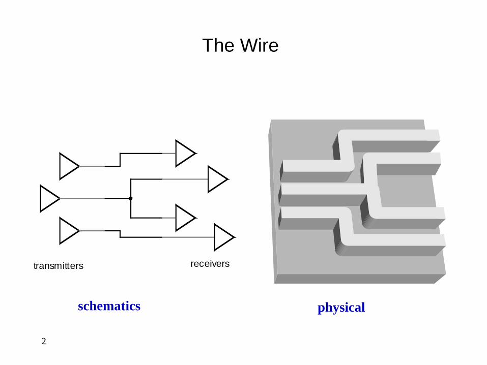
The Wire
transmitters receivers
schematics physical

3
Interconnect Impact on Chip

4
Wire Models
All-inclusive model Capacitance-only
5
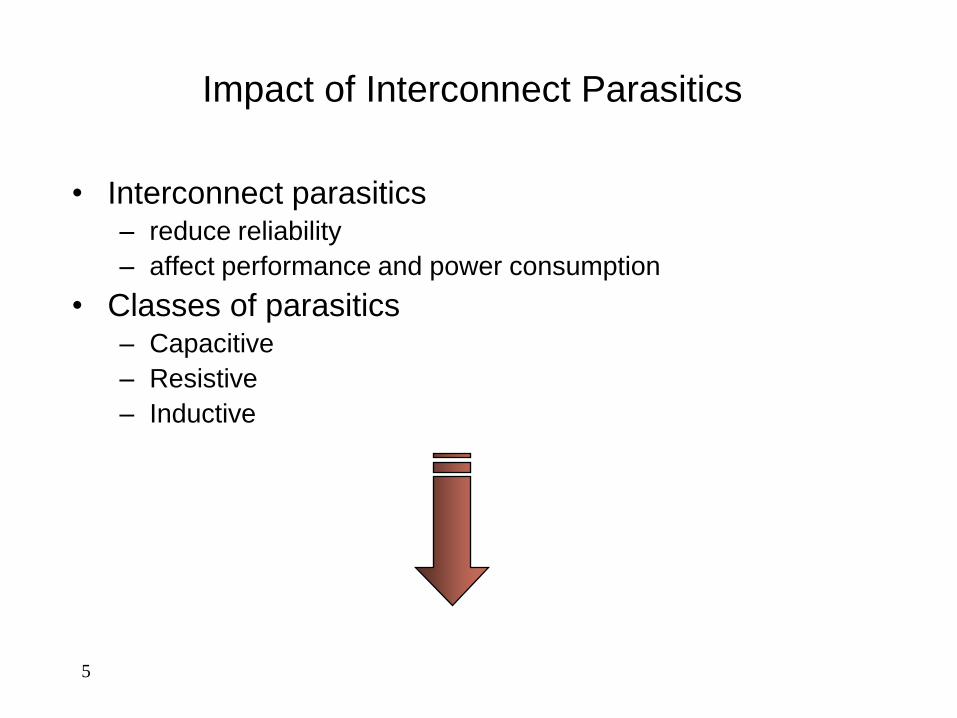
Impact of Interconnect Parasitics
• Interconnect parasitics – reduce reliability
– affect performance and power consumption
• Classes of parasitics – Capacitive
– Resistive
– Inductive
6
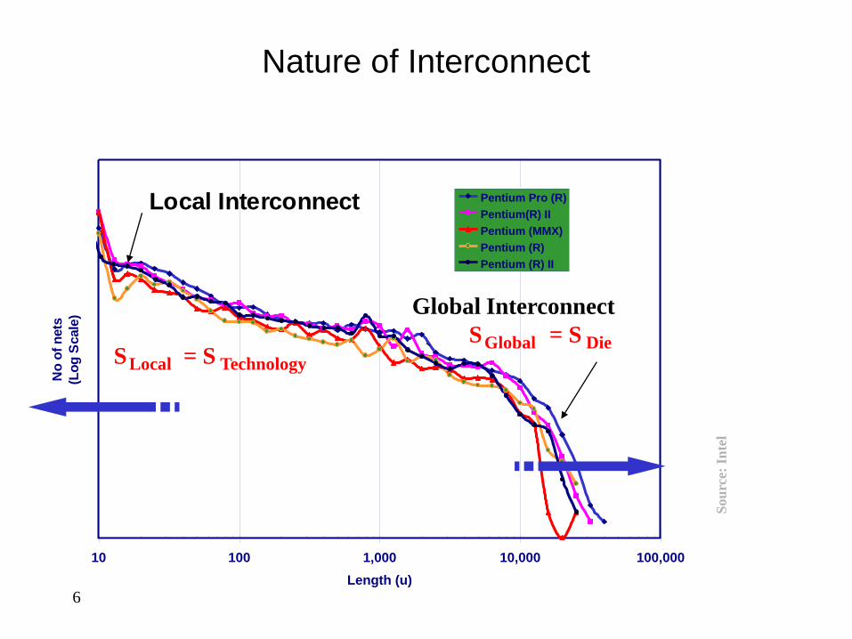
10 100 1,000 10,000 100,000
Length (u)
No
of
nets
(Lo
g S
cale
)
Pentium Pro (R)
Pentium(R) II
Pentium (MMX)
Pentium (R)
Pentium (R) II
Nature of Interconnect
Local Interconnect
Global Interconnect
S Local = S Technology
S Global = S Die
Sou
rce:
In
tel
7
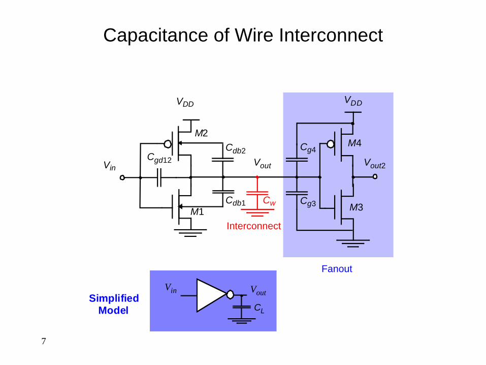
Capacitance of Wire Interconnect
VDDVDD
VinVout
M1
M2
M3
M4Cdb2
Cdb1
Cgd12
Cw
Cg4
Cg3
Vout2
Fanout
Interconnect
VoutVin
CL
SimplifiedModel

8
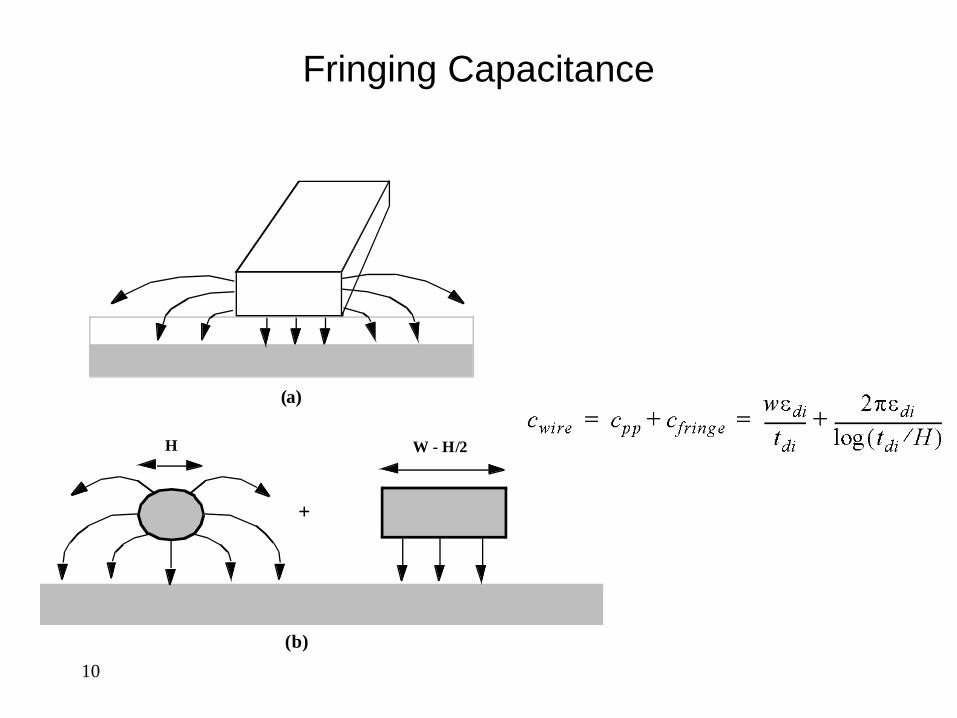
Capacitance: The Parallel Plate
Model
Dielectric
Substrate
L
W
H
tdi
Electrical-field lines
Current flow
WLt
cdi
diint
LL
CwireSSS
SS
1

9
Permittivity
10
Fringing Capacitance
W - H/2H
+
(a)
(b)

11
Interwire Capacitance
fringing parallel

Cascading Inverter Stages: driving small cap. load
Source: Intel
Prof. Kaushik Roy
@ Purdue Univ.
VDD VDD 2
PHLPLHp
ttt
))(
1
)(
1(
2 22
tpDDptnDDn
DDL
VVkVVk
VC
)11
(2 pnDD
L
kkV
C
DDT VV for
wgngpdndpL CCCCCC )()( 2211
n
p
LW
LW
)(
)(
p transistor are α times
larger than n transistor
Recall:

Cascading Inverter Stages
Source: Intel
Prof. Kaushik Roy
@ Purdue Univ.
n
p
LW
LW
)(
)(
p transistor are α times
larger than n transistor
gngp CC dndp CC and
wgndnL CCCC ))(1(
wn CC )1( gndnn CCC where

Cascoding Inverter Stages
Source: Intel
Prof. Kaushik Roy
@ Purdue Univ.
)11
(2
)1(
pnDD
wnp
kkV
CCt
)
11(
2
)1(
nDD
wn
kV
CC
0
ptset for opt
nnk ppk ( , )

Large Load
Source: Intel
Prof. Kaushik Roy
@ Purdue Univ.
VDD
Find optimum value for “u”
CL Ci 1
α
iL CxC
VDD
CL
VDD
1
α
u
uα
pt
bufpinvpp ttt __
Vin Vout

Large Load
Source: Intel
Prof. Kaushik Roy
@ Purdue Univ.
set
VDD
Ci CL
VDD
1
α
u
uα
pot = prop. delay of minimum sized inverter with
single minimum sized inverter as fan-out
popopop tu
xut
u
xtut )(

Large Load
Prof. Kaushik Roy
@ Purdue Univ.
set to get 0
u
t p
optu
pop tu
xut )(
xuop xtt opoptp 2_
When does it make sense to introduce buffer
xttx popo 2
Inserting buffer makes sense when x > 4

Multiple Stages
Prof. Kaushik Roy
@ Purdue Univ.
Gradually scale up all the devices by a constant factor “u”
postagep tut _
N stages : in
N
inL CuxCC )(
)ln(
uin
xN
popop tuu
xtuNt
)ln(
)ln(
to get 0
u
t p
optuoptu = e = 2.718282∙∙∙
po
i
Lpooptp t
C
Cetxet )ln()ln(_
u
u/ln(u)
(e,1)

Using Cascoded Buffers
Prof. Kaushik Roy
@ Purdue Univ.
invCx

tp in Fuction of ‘u’ and ‘x’
Prof. Kaushik Roy
@ Purdue Univ.
popop tuu
xtuNt
)ln(
)ln(
)ln(
)ln(
u
x
t
t
po
p

tp in Fuction of ‘u’ and ‘x’
Prof. Kaushik Roy
@ Purdue Univ.
Assumptions:
Ignored the output diffusion capacitance
The capacitance at each stage is (u + a)Ci
factor due to the
diffusion capacitance

Impact of Cascoding Buffers
Prof. Kaushik Roy
@ Purdue Univ.
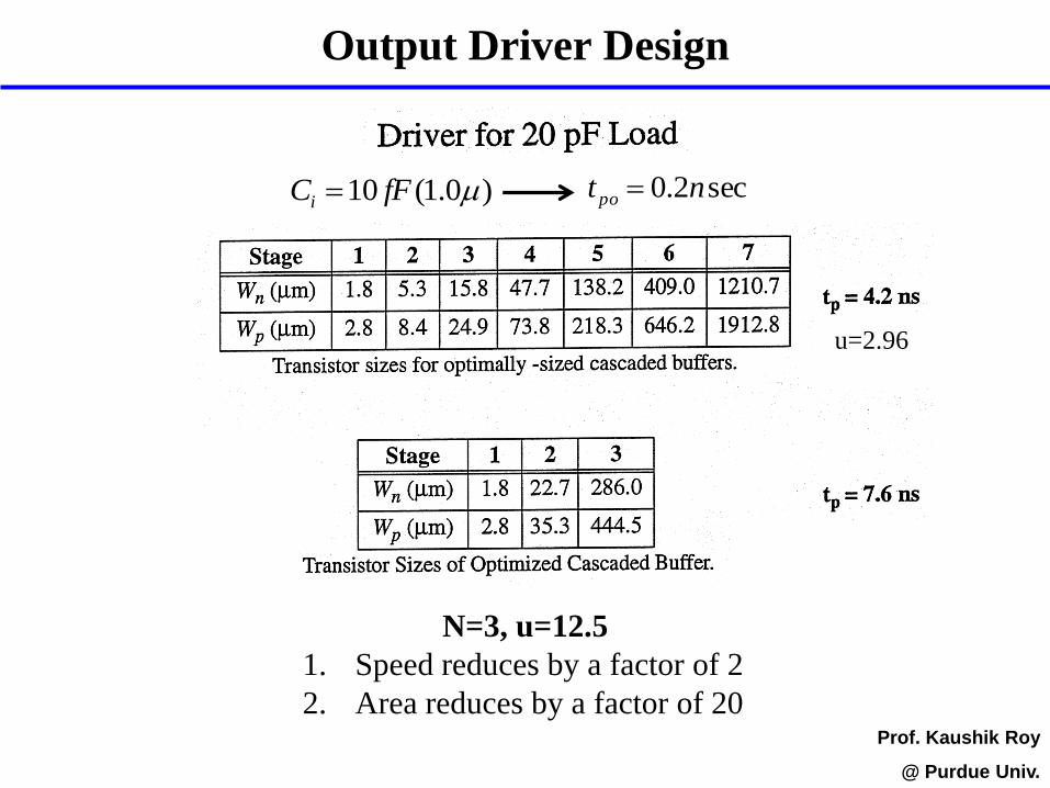
Output Driver Design
Prof. Kaushik Roy
@ Purdue Univ.
)0.1(10 fFCi sec2.0 nt po
u=2.96
N=3, u=12.5
1. Speed reduces by a factor of 2
2. Area reduces by a factor of 20
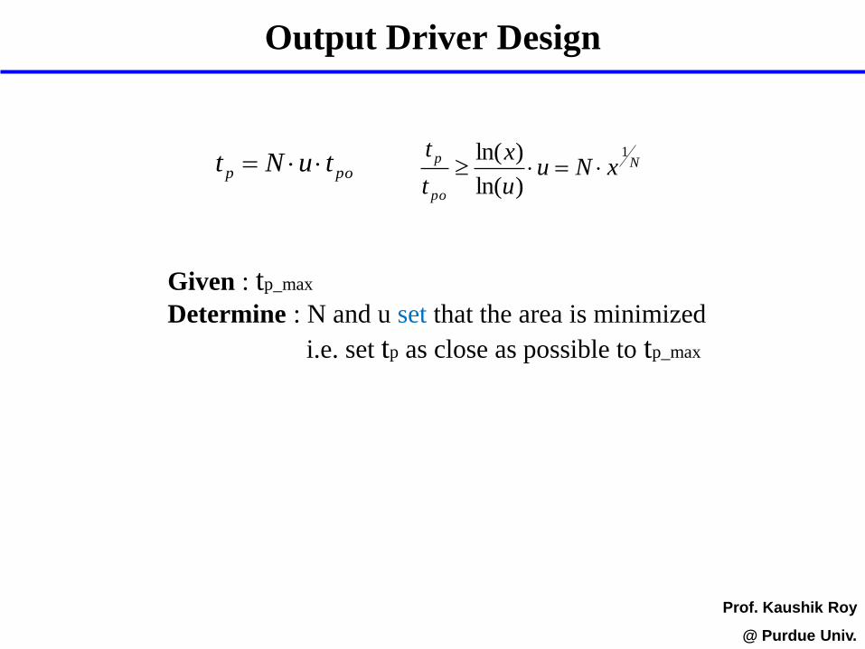
Output Driver Design
Prof. Kaushik Roy
@ Purdue Univ.
pop tuNt N
po
pxNu
u
x
t
t 1
)ln(
)ln(
Given : tp_max
Determine : N and u set that the area is minimized
i.e. set tp as close as possible to tp_max
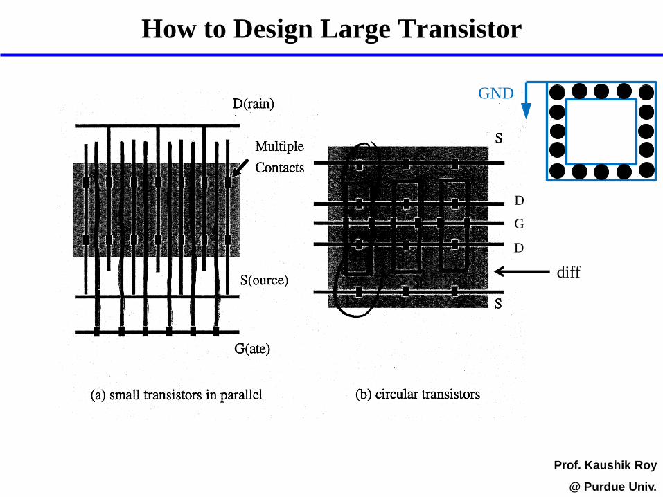
How to Design Large Transistor
Prof. Kaushik Roy
@ Purdue Univ.
D
G
D
diff
D
GND
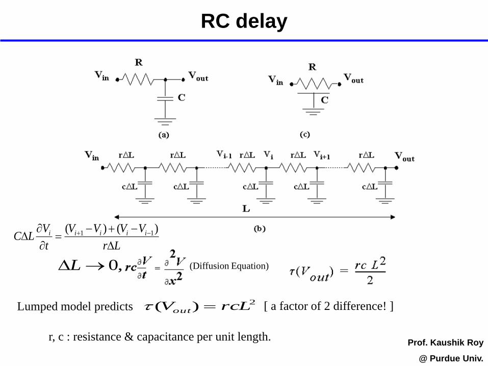
RC delay
Source: Intel
Prof. Kaushik Roy
@ Purdue Univ.
Lr
VVVV
t
VLC iiiii
)()( 11
,0L (Diffusion Equation)
Lumped model predicts 2)( rcLVout [ a factor of 2 difference! ]
r, c : resistance & capacitance per unit length.
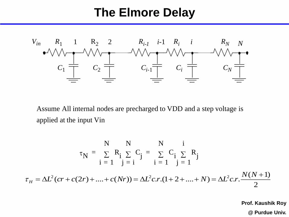
The Elmore Delay
Source: Intel
Prof. Kaushik Roy
@ Purdue Univ.
R1
C1
R2
C2
Ri-1
Ci-1
Ri
Ci
RN
CN
Vin N1 2 i-1 i
Assume All internal nodes are precharged to VDD and a step voltage is
applied at the input Vin
NR
iC
jj i=
N
i 1=
N
Ci
Rj
j 1=
i
i 1=
N
= =
2
)1(..)....21.(.))(....)2(( 222
NN
rcLNrcLNrcrccrLH
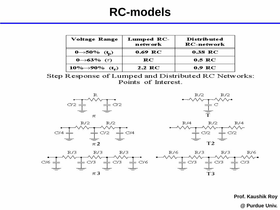
RC-models
Source: Intel
Prof. Kaushik Roy
@ Purdue Univ.
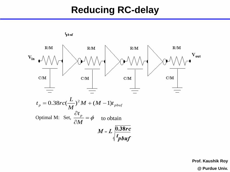
Reducing RC-delay
Source: Intel
Prof. Kaushik Roy
@ Purdue Univ.
pbufp tMMM
Lrct )1()(38.0 2
M
t pOptimal M: Set, to obtain
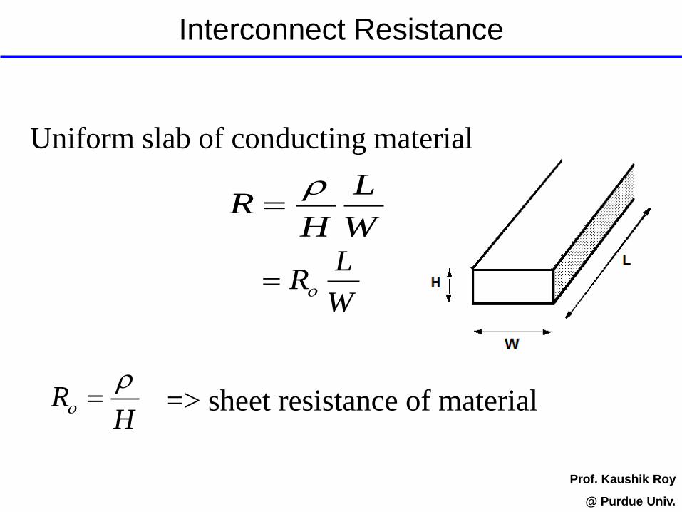
Interconnect Resistance
Source: Intel
Prof. Kaushik Roy
@ Purdue Univ.
Uniform slab of conducting material
=> sheet resistance of material
W
L
HR
W
LR
HR

Interconnect Resistance
Source: Intel
Prof. Kaushik Roy
@ Purdue Univ.
- Transition between layers add contact resistance
- Avoid excess contacts by using a single layer as much as possible
- contact resistance for min sized contacts : , for
metal1 to n+, p+ or polysilicon, for metal1 to metal2
- Full scaling of the technology increases Ro as H .
H , W , but L scales by
For local interconnects , hence, R grows linearly with scaling
factor S for local interconnects.
LS
SSL
LS
S 2
W
L
HR
211
2

Interconnect Resistance
Source: Intel
Prof. Kaushik Roy
@ Purdue Univ.
Length scaling 2S
SS L
R S
SS L
V
SSS RV
2S
S
W
L
HR L
W
LRR

Global Interconnects
Source: Intel
Prof. Kaushik Roy
@ Purdue Univ.
- length tends to grow proportionally to die size
If,
Effect: - Increased propagation delay
- Resistive voltage drop
Recall,
hence,
For local interconnects,
Hence, RC delay remains constant for local interconnects !
But intrinsic gate delay decreases !
SSL
1
L
Lwirec
SS
SS
S1
1
,
L
RCS
SS
2
SSL
LS
SR
2
3SR

Global Interconnects
Source: Intel
Prof. Kaushik Roy
@ Purdue Univ.
Hence, degradation in performances due to interconnects is very
important !!
Voltage drop
Any current decreases with S, when voltage levels are scaled by S.
for local interconnects and
hence,
3SSR
4SSRC
IRV .
SSS
L
V
1
SSL
1
1VS
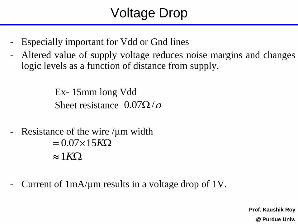
Voltage Drop
Source: Intel
Prof. Kaushik Roy
@ Purdue Univ.
- Especially important for Vdd or Gnd lines
- Altered value of supply voltage reduces noise margins and changes logic levels as a function of distance from supply.
Ex- 15mm long Vdd
Sheet resistance
- Resistance of the wire /µm width
- Current of 1mA/µm results in a voltage drop of 1V.
/07.0
K1507.0
K1
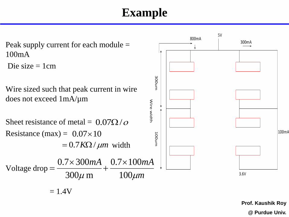
Example
Source: Intel
Prof. Kaushik Roy
@ Purdue Univ.
Peak supply current for each module =
100mA
Die size = 1cm
Wire sized such that peak current in wire
does not exceed 1mA/µm
Sheet resistance of metal =
Resistance (max) =
width
Voltage drop
= 1.4V
m
mAmA
100
1007.0
m300
3007.0
1007.0
mK /7.0
/07.0
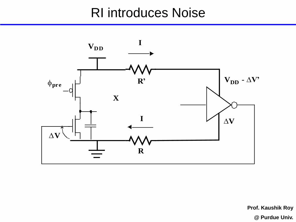
RI introduces Noise
Source: Intel
Prof. Kaushik Roy
@ Purdue Univ.
VDD
X
I
I
R’
R
VDD - V’
V
V
pre
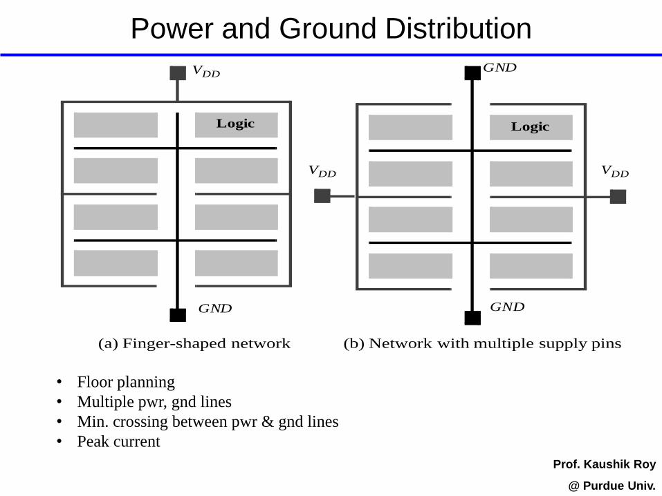
Power and Ground Distribution
Source: Intel
Prof. Kaushik Roy
@ Purdue Univ.
GND
VDD
Logic
GND
VDD
Logic
GND
VDD
(a) Finger-shaped network (b) Network with multiple supply pins
• Floor planning
• Multiple pwr, gnd lines
• Min. crossing between pwr & gnd lines
• Peak current

Electro migration (1)
Source: Intel
Prof. Kaushik Roy
@ Purdue Univ.
Limits dc-current to 1 mA/m

Electro migration (2)
Source: Intel
Prof. Kaushik Roy
@ Purdue Univ.
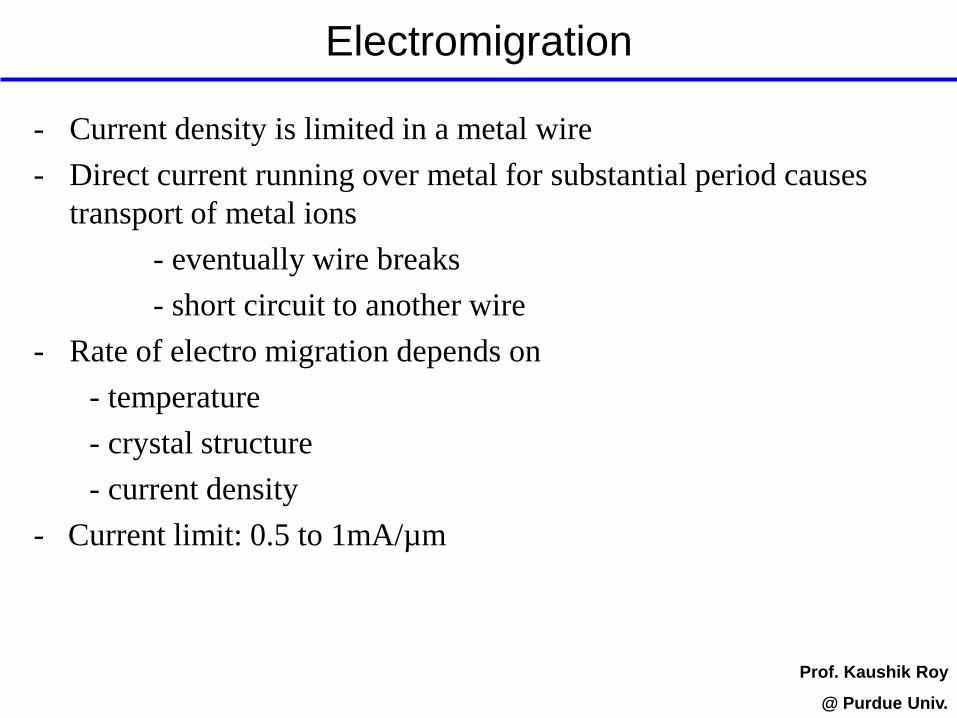
Electromigration
Source: Intel
Prof. Kaushik Roy
@ Purdue Univ.
- Current density is limited in a metal wire
- Direct current running over metal for substantial period causes
transport of metal ions
- eventually wire breaks
- short circuit to another wire
- Rate of electro migration depends on
- temperature
- crystal structure
- current density
- Current limit: 0.5 to 1mA/µm
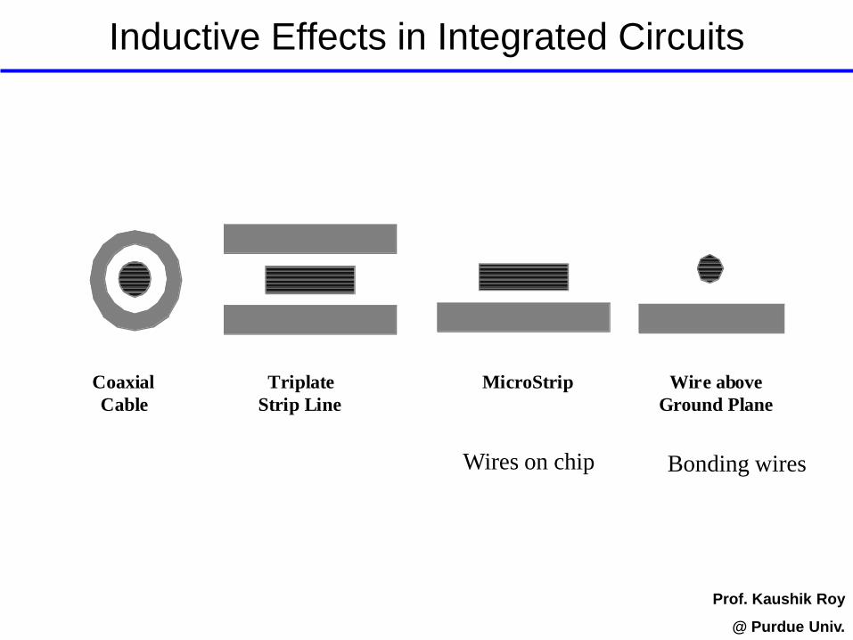
Inductive Effects in Integrated Circuits
Source: Intel
Prof. Kaushik Roy
@ Purdue Univ.
Coaxial
Cable
Triplate
Strip Line
MicroStrip Wire above
Ground Plane
Wires on chip Bonding wires
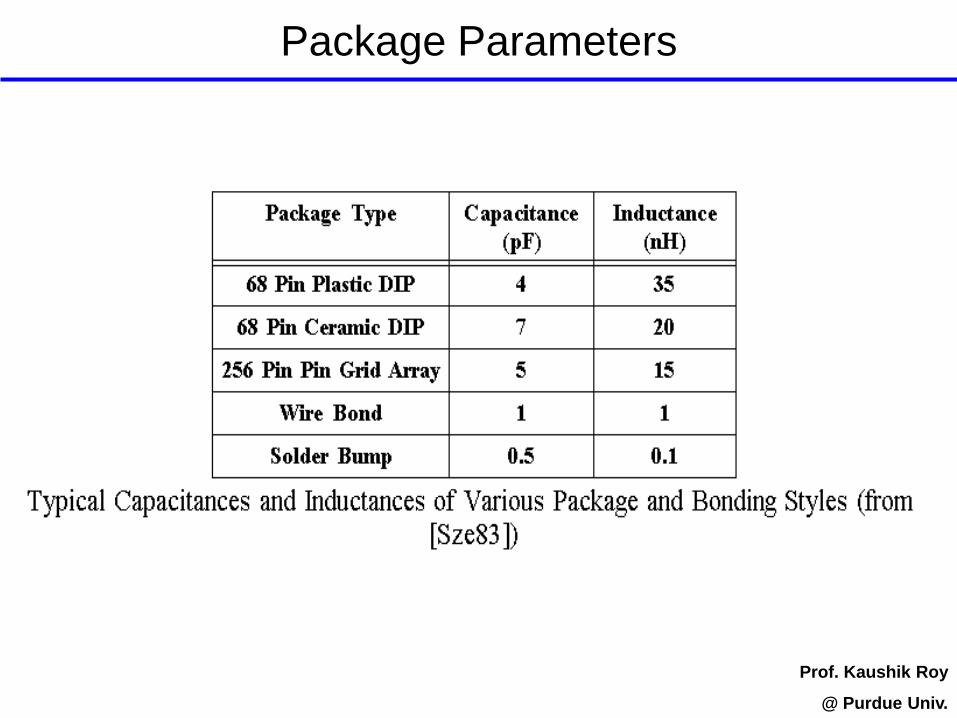
Package Parameters
Source: Intel
Prof. Kaushik Roy
@ Purdue Univ.
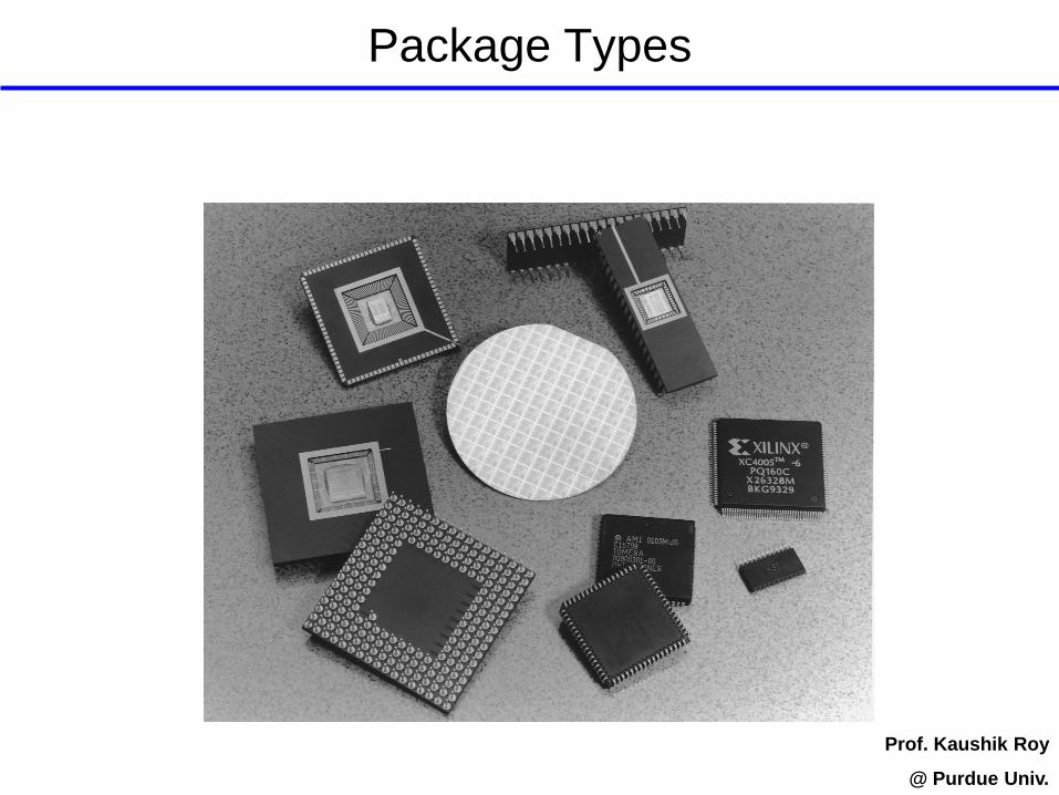
Package Types
Source: Intel
Prof. Kaushik Roy
@ Purdue Univ.

L di/dt
Source: Intel
Prof. Kaushik Roy
@ Purdue Univ.
VDD
L
L
VoutVin
CL
i(t)
)(til
)(tvL dt
diLtV L
L )(External
DDV
Change in transient current creates
a voltage difference between the
external and internal supply
voltages.
Situation is severe at output pads!
• Large capacitance
• Larger current surge
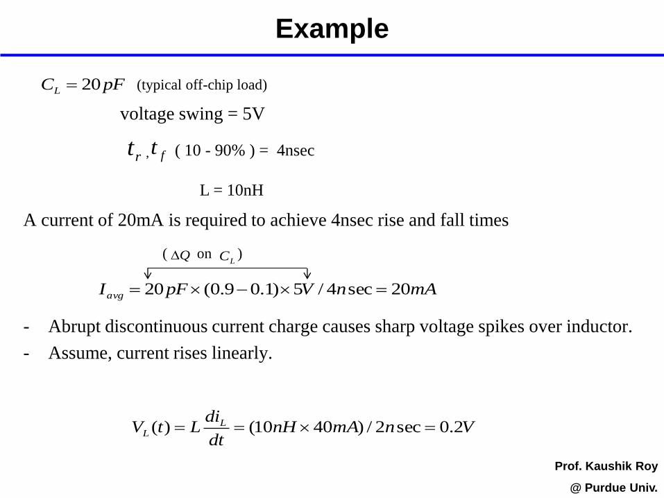
Example
Source: Intel
Prof. Kaushik Roy
@ Purdue Univ.
voltage swing = 5V
A current of 20mA is required to achieve 4nsec rise and fall times
- Abrupt discontinuous current charge causes sharp voltage spikes over inductor.
- Assume, current rises linearly.
pFCL 20
VnmAnHdt
diLtV L
L 2.0sec2/)4010()(
(typical off-chip load)
rt ft ( 10 - 90% ) = 4nsec
L = 10nH
,
mAnVpFIavg 20sec4/5)1.09.0(20
( on ) QLC

L di/dt
Source: Intel
Prof. Kaushik Roy
@ Purdue Univ.
A single supply pin may serve a large no. of gates or output
drivers.
• Simultaneous switching can cause worse current transients
and voltage drop.
• Internal supplies derived from external ones.
Eg. Simultaneous switching of 16 drivers of output bus
would cause a voltage drop of 1.5V.

L di/dt: Simulation
Source: Intel
Prof. Kaushik Roy
@ Purdue Univ.
t
t
t
vout
iL
vL
20mA
40mA
5V
0.2V
0.0
1.0
2.0
3.0
4.0
5.0
Vou
t(V)
0
10
20
I L (m
A)
2 4 6 8 10t (nsec)
-0.3
-0.1
0.1
0.3
0.5
VL(V
)
tfall = 0.5 nsec
tfall = 4 nsec
Signals Waveforms for Output Driver connected To Bonding Pads
(a) vout; (b) iL and (c) vL.
The Results of an Actual Simulation are Shown on the Right Side.

Solutions
Source: Intel
Prof. Kaushik Roy
@ Purdue Univ.
1. Separate power pins for I/O pads and chip core.
1. Multiple power and ground pins.
- typical no. are 5 to 10 drivers per supply pin.
3. Careful selection of positions of the power and ground pins on package.
4. Adding decoupling capacitance.
- low pass network.
5. Increase rise and fall times as much as possible (off-chip signal).
6. Advanced packaging.
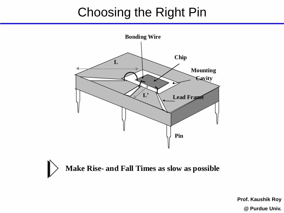
Choosing the Right Pin
Source: Intel
Prof. Kaushik Roy
@ Purdue Univ.
Chip
Mounting
Cavity
Lead Frame
Bonding Wire
Pin
L
L’
Make Rise- and Fall Times as slow as possible

Decoupling Capacitors
Source: Intel
Prof. Kaushik Roy
@ Purdue Univ.
CHIPSUPPLY
Bonding
Wire
Board
Wiring
Cd
Decoupling
Capacitor
+
-

The Transmission Line
Source: Intel
Prof. Kaushik Roy
@ Purdue Univ.
Vin
r l
c
r l
c
r l
c
r l
c
Voutx
g g g g
Wave propagation equation

Source: Intel
Prof. Kaushik Roy
@ Purdue Univ.
Wave Reflection

Wave Reflection
Source: Intel
R
0ZR
0
2
I
VV inc1R
= termination resistance
= reflection coefficient => fraction of voltage or current that is reflected
=> No reflection, wire appears as if length
incII
V
2
0
10R
No phase reversal
phase reversal
Reflections eventually die down
Prof. Kaushik Roy
@ Purdue Univ.
=>
=>
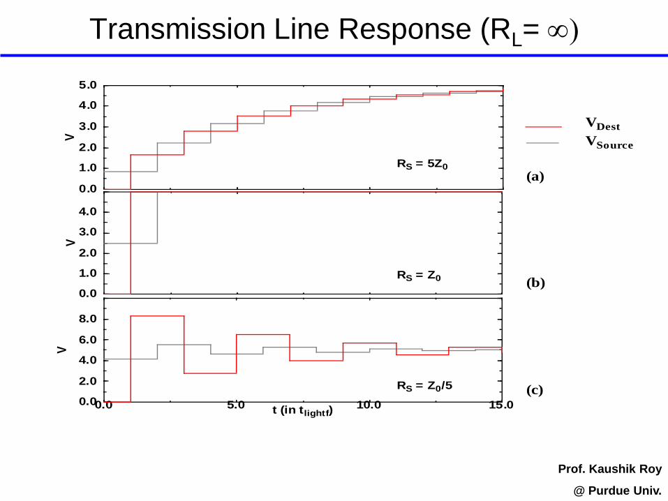
Transmission Line Response (RL= )
Source: Intel
Prof. Kaushik Roy
@ Purdue Univ.
0.0
1.0
2.0
3.0
4.0
5.0
V
0.0
1.0
2.0
3.0
4.0
V
0.0 5.0 10.0 15.0t (in tlightf)0.0
2.0
4.0
6.0
8.0
V
RS = 5Z0
RS = Z0
RS = Z0/5
(a)
(b)
(c)
VDest
VSource
Related Documents


![[C P Kaushik, S S Bhavikatti, Anubha Kaushik] Basi(BookFi.org)](https://static.cupdf.com/doc/110x72/55cf9b90550346d033a68cc1/c-p-kaushik-s-s-bhavikatti-anubha-kaushik-basibookfiorg.jpg)