Adapted from J. Rabaey et al, Digital Integrated Circuits 2nd, 2003 Prentice Hall/Pearson a.a. 2007-2008 Productivity Trends Productivity Trends 2003 1981 1983 1985 1987 1989 1991 1993 1995 1997 1999 2001 2005 2007 2009 Logic Tr./Chip Tr./Staff Month. x x x x x x x 21%/Yr. compound Productivity growth rate x 58%/Yr. compounded Complexity growth rate 10,000 1,000 100 10 1 0.1 0.01 0.001 Logic Transistor per Chip (M) 0.01 0.1 1 10 100 1,000 10,000 100,000 Productivity (K) Trans./Staff - Mo. Source: Sematech Complexity outpaces design productivity Complexity Courtesy, ITRS Roadmap Adapted from J. Rabaey et al, Digital Integrated Circuits 2nd, 2003 Prentice Hall/Pearson a.a. 2007-2008 Livelli di astrazione di un sistema Livelli di astrazione di un sistema digitale digitale n+ n+ S G D + DEVICE CIRCUIT GATE RTL (Register Transfer Level) SYSTEM q=a*b+c

Welcome message from author
This document is posted to help you gain knowledge. Please leave a comment to let me know what you think about it! Share it to your friends and learn new things together.
Transcript

Adapted from J. Rabaey et al, Digital Integrated Circuits2nd, 2003 Prentice Hall/Pearson a.a. 2007-2008
Productivity TrendsProductivity Trends
2003
1981
1983
1985
1987
1989
1991
1993
1995
1997
1999
2001
2005
2007
2009
Logic Tr./ChipTr./Staff Month.
xxx
xxx
x
21%/Yr. compoundProductivity growth rate
x
58%/Yr. compoundedComplexity growth rate
10,000
1,000
100
10
1
0.1
0.01
0.001
Lo
gic
Tra
nsi
sto
r p
er C
hip
(M)
0.01
0.1
1
10
100
1,000
10,000
100,000
Pro
du
ctiv
ity
(K)
Tra
ns.
/Sta
ff -
Mo
.
Source: Sematech
Complexity outpaces design productivity
Co
mp
lexi
ty
Courtesy, ITRS Roadmap
Adapted from J. Rabaey et al, Digital Integrated Circuits2nd, 2003 Prentice Hall/Pearson a.a. 2007-2008
Livelli di astrazione di un sistema Livelli di astrazione di un sistema digitaledigitale
n+n+S
GD
+
DEVICE
CIRCUIT
GATE
RTL (Register Transfer Level)
SYSTEMq=a*b+c
Adapted from J. Rabaey et al, Digital Integrated Circuits2nd, 2003 Prentice Hall/Pearson a.a. 2007-2008
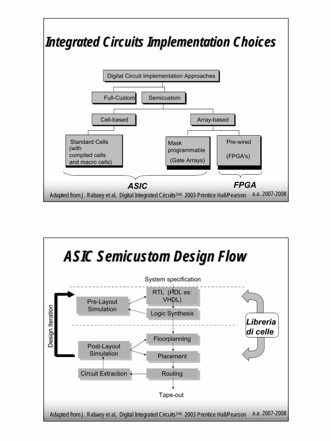
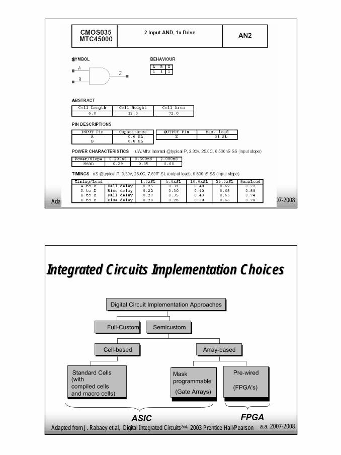
Integrated Circuits Implementation ChoicesIntegrated Circuits Implementation Choices
Full-Custom
Standard Cells(withcompiled cellsand macro cells)
Cell-based
Maskprogrammable
(Gate Arrays)
Pre-wired
(FPGA's)
Array-based
Semicustom
Digital Circuit Implementation Approaches
ASIC FPGA
Adapted from J. Rabaey et al, Digital Integrated Circuits2nd, 2003 Prentice Hall/Pearson a.a. 2007-2008
ASIC ASIC SemicustomSemicustom Design FlowDesign Flow
RTL (HDL es: VHDL)
Logic Synthesis
Floorplanning
Placement
Routing
Tape-out
Circuit Extraction
Pre-Layout Simulation
Post-Layout Simulation
System specification
Des
ign
Itera
tion
Des
ign
Itera
tion
Libreriadi celle

Adapted from J. Rabaey et al, Digital Integrated Circuits2nd, 2003 Prentice Hall/Pearson a.a. 2007-2008
FPGA Design FlowFPGA Design Flow
RTL (HDL es: VHDL)
Logic Synthesis
Programming -file
System specification
blocchilogici
elementari
Adapted from J. Rabaey et al, Digital Integrated Circuits2nd, 2003 Prentice Hall/Pearson a.a. 2007-2008
The Custom Approach (old)The Custom Approach (old)
Intel 4004
Courtesy Intel

Adapted from J. Rabaey et al, Digital Integrated Circuits2nd, 2003 Prentice Hall/Pearson a.a. 2007-2008
Today: full custom design only for Today: full custom design only for modules modules
q reuseq regularityq very high performance q (analog block)
Adapted from J. Rabaey et al, Digital Integrated Circuits2nd, 2003 Prentice Hall/Pearson a.a. 2007-2008
Full custom designFull custom design
q Standard cells § Combinational and sequential logic gates
q I/O padsq Memory compilers and array structures§ SRAM, dual port SRAM, register files, Cache controllers§ PLD
q Arithmetic Buildings blocks§ Adders, multipliers, shifters
q FPGA logic element q Analog modules§ Example: PLL, A/D, D/A

Adapted from J. Rabaey et al, Digital Integrated Circuits2nd, 2003 Prentice Hall/Pearson a.a. 2007-2008
Transition to Automation and Regular StructuresTransition to Automation and Regular Structures
Intel 4004 (‘71)Intel 4004 (‘71)Intel 8080Intel 8080 Intel 8085Intel 8085
Intel 8286Intel 8286 Intel 8486Intel 8486Courtesy Intel
Adapted from J. Rabaey et al, Digital Integrated Circuits2nd, 2003 Prentice Hall/Pearson a.a. 2007-2008

Adapted from J. Rabaey et al, Digital Integrated Circuits2nd, 2003 Prentice Hall/Pearson a.a. 2007-2008
Adapted from J. Rabaey et al, Digital Integrated Circuits2nd, 2003 Prentice Hall/Pearson a.a. 2007-2008
Progetto gerarchicoProgetto gerarchico

Adapted from J. Rabaey et al, Digital Integrated Circuits2nd, 2003 Prentice Hall/Pearson a.a. 2007-2008
LibreriaLibreria di Standard Cellsdi Standard Cells
q Esempio: libreria AMS 0.35um 250 celle elementari§ Celle combinatorie:
5 inverters, 14 buffers, 8 buffer tri-state, 21 and, 21 or, 12 xor, 21 nand, 21 nor, 6 mux,28 blocchi misti (half-adder, full-adder,..)§ Celle sequenziali:
8 FF JK, 32 FF D§ IO pads:
10 Inout, 12 Inputs, 10 outputs, 6 power
Adapted from J. Rabaey et al, Digital Integrated Circuits2nd, 2003 Prentice Hall/Pearson a.a. 2007-2008
Adapted from J. Rabaey et al, Digital Integrated Circuits2nd, 2003 Prentice Hall/Pearson a.a. 2007-2008
Adapted from J. Rabaey et al, Digital Integrated Circuits2nd, 2003 Prentice Hall/Pearson a.a. 2007-2008
Integrated Circuits Implementation ChoicesIntegrated Circuits Implementation Choices
Full-Custom
Standard Cells(withcompiled cellsand macro cells)
Cell-based
Maskprogrammable
(Gate Arrays)
Pre-wired
(FPGA's)
Array-based
Semicustom
Digital Circuit Implementation Approaches
ASIC FPGA

Adapted from J. Rabaey et al, Digital Integrated Circuits2nd, 2003 Prentice Hall/Pearson a.a. 2007-2008
CellCell--based (or standard cells): core area and based (or standard cells): core area and pin number depend on the applicationpin number depend on the application
Pad
Core area
die
Adapted from J. Rabaey et al, Digital Integrated Circuits2nd, 2003 Prentice Hall/Pearson a.a. 2007-2008
CellCell--based (or standard cells) layoutbased (or standard cells) layout(old generation)(old generation)
Routing channel requirements arereduced by presenceof more interconnectlayers
Functionalmodule(RAM,multiplier, …)
Routingchannel
Logic cellFeedthrough cell
Row
s of
cel
ls

Adapted from J. Rabaey et al, Digital Integrated Circuits2nd, 2003 Prentice Hall/Pearson a.a. 2007-2008
Standard Cell Standard Cell –– The New GenerationThe New Generation
Cell-structurehidden underinterconnect layers
Adapted from J. Rabaey et al, Digital Integrated Circuits2nd, 2003 Prentice Hall/Pearson a.a. 2007-2008
Compiled cellsCompiled cells
256×32 (or 8192 bit) SRAMGenerated by hard-macro module compiler
Adapted from J. Rabaey et al, Digital Integrated Circuits2nd, 2003 Prentice Hall/Pearson a.a. 2007-2008
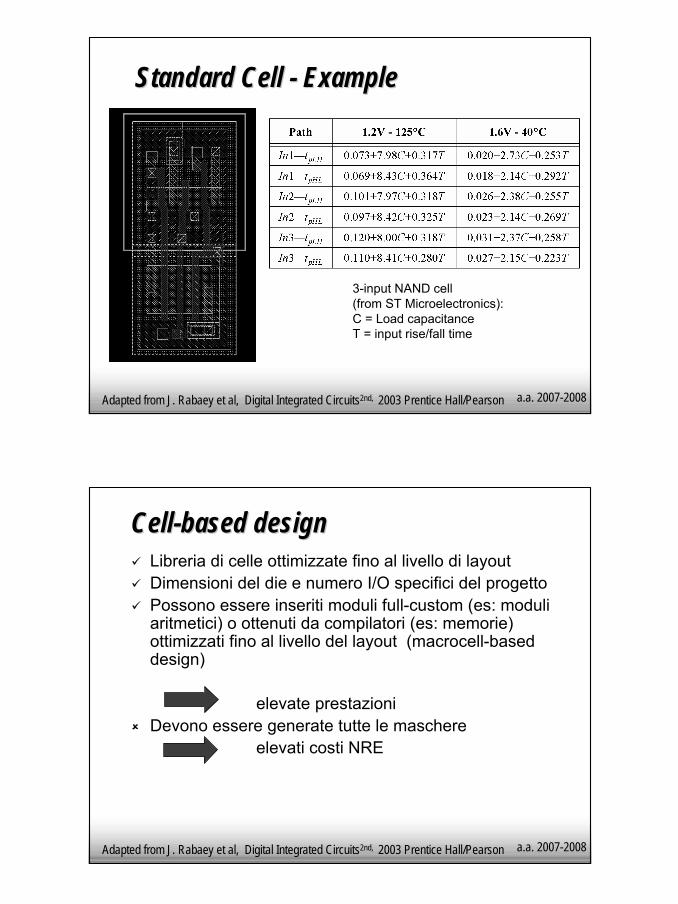
Standard Cell Standard Cell -- ExampleExample
3-input NAND cell(from ST Microelectronics):C = Load capacitanceT = input rise/fall time
Adapted from J. Rabaey et al, Digital Integrated Circuits2nd, 2003 Prentice Hall/Pearson a.a. 2007-2008
CellCell--based designbased designü Libreria di celle ottimizzate fino al livello di layoutü Dimensioni del die e numero I/O specifici del progettoü Possono essere inseriti moduli full-custom (es: moduli
aritmetici) o ottenuti da compilatori (es: memorie) ottimizzati fino al livello del layout (macrocell-baseddesign)
elevate prestazioniû Devono essere generate tutte le maschere
elevati costi NRE

Adapted from J. Rabaey et al, Digital Integrated Circuits2nd, 2003 Prentice Hall/Pearson a.a. 2007-2008
Mask-programmable(Gate Arrays)
Pre-wired(FPGA's)
Array-based
ArrayArray--based Implementationbased Implementation
ASIC
Adapted from J. Rabaey et al, Digital Integrated Circuits2nd, 2003 Prentice Hall/Pearson a.a. 2007-2008
ArrayArray basedbased: : fixedfixed I/O, I/O, fixedfixed core area core area
Pad
Core area
die
Adapted from J. Rabaey et al, Digital Integrated Circuits2nd, 2003 Prentice Hall/Pearson a.a. 2007-2008
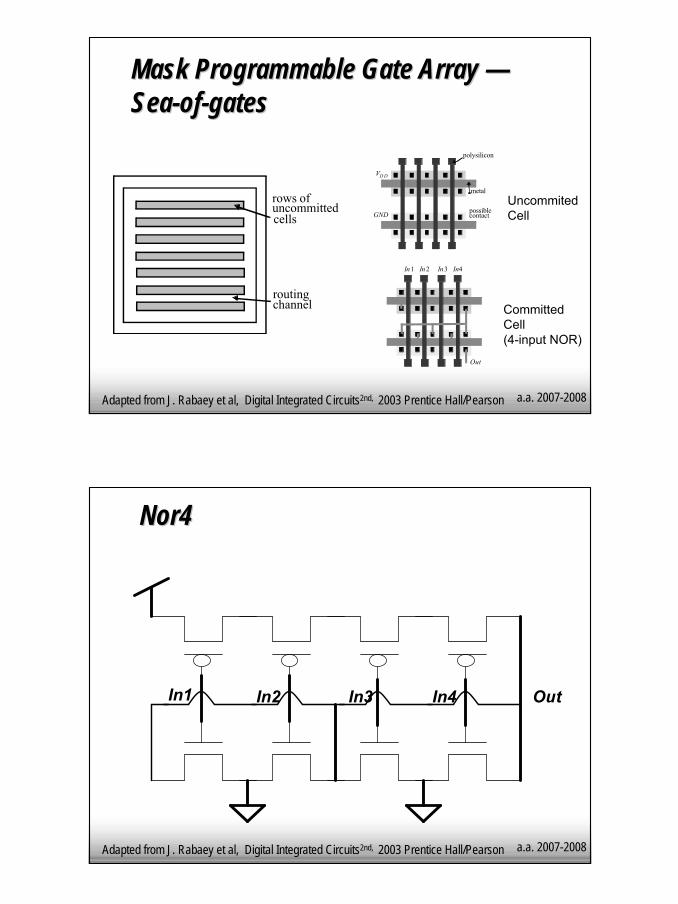
Mask Programmable Gate Array Mask Programmable Gate Array ——SeaSea--ofof--gatesgates
rows of
cells
routing channel
uncommitted
VD D
GND
polysilicon
metal
possiblecontact
In1 In2 In3 In4
Out
UncommitedCell
CommittedCell(4-input NOR)
Adapted from J. Rabaey et al, Digital Integrated Circuits2nd, 2003 Prentice Hall/Pearson a.a. 2007-2008
Nor4 Nor4
In1 In2 OutIn3 In4

Adapted from J. Rabaey et al, Digital Integrated Circuits2nd, 2003 Prentice Hall/Pearson a.a. 2007-2008
IsolamentoIsolamento elettricoelettrico: : esempioesempio cellacellainvertitoreinvertitore
In Out
Adapted from J. Rabaey et al, Digital Integrated Circuits2nd, 2003 Prentice Hall/Pearson a.a. 2007-2008
IsolamentoIsolamento elettricoelettrico: : esempioesempio (1) (1) reterete ottenutaottenuta istanziandoistanziando due due cellecelle NOTNOT
Non Non realizzarealizza la la funzionefunzionevolutavoluta !!

Adapted from J. Rabaey et al, Digital Integrated Circuits2nd, 2003 Prentice Hall/Pearson a.a. 2007-2008
IsolamentoIsolamento elettricoelettrico: : esempioesempio (2) (2) reterete ottenutaottenuta istanziandoistanziando due due cellecelle NOTNOT
malfunzionamentomalfunzionamentose i se i transistoritransistori M1 e P1 M1 e P1 entranoentranoin in conduzioneconduzione
P1
M1
Adapted from J. Rabaey et al, Digital Integrated Circuits2nd, 2003 Prentice Hall/Pearson a.a. 2007-2008
IsolamentoIsolamento elettricoelettrico: : cellacella inverter con inverter con transistoritransistori di di isolamentoisolamento

Adapted from J. Rabaey et al, Digital Integrated Circuits2nd, 2003 Prentice Hall/Pearson a.a. 2007-2008
IsolamentoIsolamento elettricoelettrico: : reterete ottenutaottenuta istanziandoistanziandodue due cellecelle con con transistoritransistori di di isolamentoisolamento
funzionafunziona !!
Adapted from J. Rabaey et al, Digital Integrated Circuits2nd, 2003 Prentice Hall/Pearson a.a. 2007-2008
SeaSea--ofof--gate Primitive Cellsgate Primitive Cells
NMOS
PMOS
Oxide-isolation
PMOS
NMOS
NMOS
Using oxide-isolation Using gate-isolation

Adapted from J. Rabaey et al, Digital Integrated Circuits2nd, 2003 Prentice Hall/Pearson a.a. 2007-2008
IsolamentoIsolamento elettricoelettrico: : isolamentoisolamento tramitetramitearea area attivaattiva
Adapted from J. Rabaey et al, Digital Integrated Circuits2nd, 2003 Prentice Hall/Pearson a.a. 2007-2008
IsolamentoIsolamento elettricoelettrico tramitetramite area area attivaattiva: : InverterInverter
I I transistoritransistori adiacentiadiacenti M1 e P1 non M1 e P1 non possonopossono essereessere utilizzatiutilizzati
P1
M1

Adapted from J. Rabaey et al, Digital Integrated Circuits2nd, 2003 Prentice Hall/Pearson a.a. 2007-2008
IsolamentoIsolamento elettricoelettrico tramitetramite area area attivaattiva: : Nand2Nand2
PossonoPossono essereessere istanziateistanziate due due cellecelleconsecutivamenteconsecutivamente
Adapted from J. Rabaey et al, Digital Integrated Circuits2nd, 2003 Prentice Hall/Pearson a.a. 2007-2008
SeaSea--ofof--gates (new generation) gates (new generation)
Random Logic
MemorySubsystem
LSI Logic LEA300K(0.6 µm CMOS)
Courtesy LSI Logic

Adapted from J. Rabaey et al, Digital Integrated Circuits2nd, 2003 Prentice Hall/Pearson a.a. 2007-2008
MaskMask--programmable gateprogrammable gate--arrayarrayü Le porte logiche sono realizzate a partire da una cella
elementare di dimensione fissata che utilizza transistori con fattore di forma predefinito
ü Dimensioni del die e numero I/O fissateü Il progetto delle macro celle è vincolato dalla struttura della cella
elementareü Isolamento o tramite transistori di isolamento o area attiva
prestazioni inferiori rispetto la metodologiaa standard-cell
û non devono essere generate tutte le maschere
costi NRE inferiori rispetto alla metodologiastandard-cell
ma è comunque necessaria interazione con la silicon foundry
Flusso di progetto uguale a quello a cell standard
Adapted from J. Rabaey et al, Digital Integrated Circuits2nd, 2003 Prentice Hall/Pearson a.a. 2007-2008
ProgrammaProgramma del del corsocorso
qProgetto e caratterizzazione di celle logicheelementari e moduli complessi utilizzabili in un flusso di progetto semi-custom§ Tecnologia: MIETEC CMOS 0.35 um§ Metodologia di progetto: Mask Programmable
Gate Array (SOG)§ CAD tools: Cadence OPUS disponibile in LAB1
– schematico, layout, simbolo– caratterizzazione mediante simulazione circuitale

Adapted from J. Rabaey et al, Digital Integrated Circuits2nd, 2003 Prentice Hall/Pearson a.a. 2007-2008
q Libri di consultazione§ J. M. Rabaey, A. Chandrakasan, B. NikolicDigital Integrated Circuits, A design Perspective (II ed)Prentice Hall Electronics 2003
q Materiale § in rete: www.deis.unibo.it > docenti > prof. II fascia >
E. Franchi § in biblioteca
– Guida agli strumenti software, alle esercitazionie caratterizzazione della tecnologia– Lucidi
§ in laboratorio– Manuale del processo MIETEC CMOS 0.35um
Adapted from J. Rabaey et al, Digital Integrated Circuits2nd, 2003 Prentice Hall/Pearson a.a. 2007-2008
q Esami: discussione dell’attività di laboratorio§ Prova intermedia : progetto e caratterizzazione di
una cella combinatoria e di una sequenzialesettimana 19-21 febbraio (quinta del corso)
§ Prova finale: progetto e caratterizzazione di un modulo complessosu appuntamento
q Username e password per ws del lab1gruppi di due
q Avvisi: tramite il portale docenti

Adapted from J. Rabaey et al, Digital Integrated Circuits2nd, 2003 Prentice Hall/Pearson a.a. 2007-200819-20
18-19
LAB ESD17-18
LAB ESD16-17
LAB ESD15-1614-15
LAB ESDESDESDESD13-14
LAB ESDESDESDESD12-13
CalcolatoriLAB ESDESDCalcolatoriESD11-12
CalcolatoriLAB ESDCalcolatoriCalcolatori10-11
CalcolatoriLAB ESDCalcolatoriCalcolatori9-10
8-9
SabatoVenerdìGiovedìMercoledìMartedìLunedìOre
Adapted from J. Rabaey et al, Digital Integrated Circuits2nd, 2003 Prentice Hall/Pearson a.a. 2007-200819-20
18-19
Turno 1BTurno 2BTurno 2A17-18
Turno 1BTurno 2BTurno 2A16-17
Turno 1BTurno 2BTurno 2A15-1614-15
Turno 1AESDESDESD13-14
Turno 1AESDESDESD12-13
CalcolatoriTurno 1AESDCalcolatoriESD11-12
CalcolatoriLAB ESDCalcolatoriCalcolatori10-11
CalcolatoriLAB ESDCalcolatoriCalcolatori9-10
8-9
SabatoVenerdìGiovedìMercoledìMartedìLunedìOre
Related Documents


