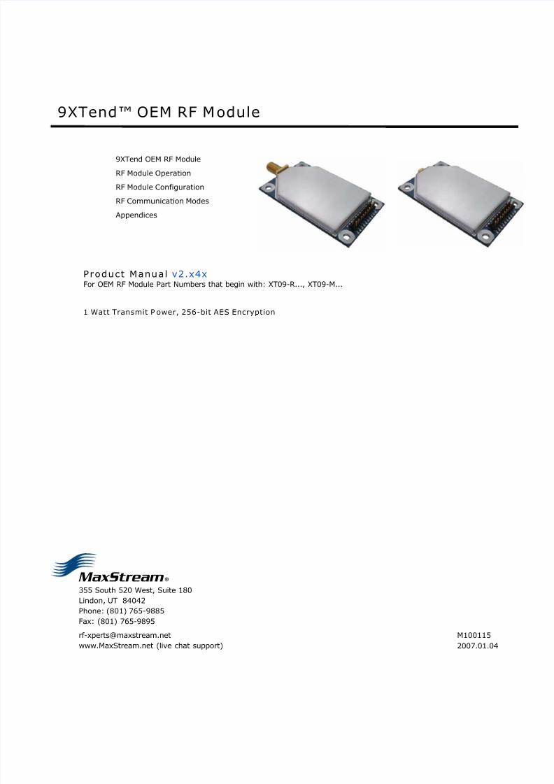
MaxStream 355 South 520 West, Suite 180 Lindon, UT 84042 Phone: (801) 765-9885 Fax: (801) 765-9895 [email protected] www.MaxStream.net (live chat support) 9XTend™ OEM RF Module 9XTend OEM RF Module RF Module Operation RF Module Configuration RF Communication Modes Appendices Product Manual v2.x4x For OEM RF Module Part Numbers that begin with: XT09-R..., XT09-M... 1 Watt Transmit P ower, 256-bit AES Encryption M100115 2007.01.04

Welcome message from author
This document is posted to help you gain knowledge. Please leave a comment to let me know what you think about it! Share it to your friends and learn new things together.
Transcript
8/3/2019 Product Manual Xtend Oem Rfmodule
http://slidepdf.com/reader/full/product-manual-xtend-oem-rfmodule 1/71
MaxStream
355 South 520 West, Suite 180
Lindon, UT 84042
Phone: (801) 765-9885
Fax: (801) 765-9895
www.MaxStream.net (live chat support)
9XTend™ OEM RF Module
9XTend OEM RF Module
RF Module Operation
RF Module Configuration
RF Communication Modes
Appendices
Product Manual v2.x4xFor OEM RF Module Part Numbers that begin with: XT09-R..., XT09-M...
1 Watt Transmit P ower, 256-bit AES Encryption
M100115
2007.01.04
8/3/2019 Product Manual Xtend Oem Rfmodule
http://slidepdf.com/reader/full/product-manual-xtend-oem-rfmodule 2/71
9XTend™ OEM RF Module ‐ Product Manual v2.x4x [2007.01.04]
© 2007
MaxStream,
Inc.,
Confidential
&
Proprietary
‐ All
Rights
Reserved
ii
© 2007 MaxStream, Inc. All rights reserved
The contents of this manual may not be transmitted or reproduced in any form or by any means without the written permission of MaxStream, Inc.
XTend™ is a trademark of MaxStream, Inc.
AES Encryption Source Code © 2007 Dr. Brian Gladman, Worcester, UK. All rights reserved.
Conditions:
‐ Distributions of AES source code include the above copyright notice, this list of conditions and disclaimer.
‐Distributions in binary form include the above copyright notice, this list of con‐
ditions and disclaimer in the documentation and/or other associated materials.
‐ The copyright holderʹs name is not used to endorse products built using this software without specific written permission.
Alternatively, provided that this notice is retained in full, this product may be dis‐tributed under the terms of the GNU General Public License (GPL), in which case the provisions of the GPL apply INSTEAD OF those given above.
Disclaimer ‐ This AES software is provided ʹas isʹwith no explicit or implied war‐ranties in respect of its properties, including, but not limited to, correctness and/or
fitness
for
purpose.
Technical Support: Phone: (801) 765‐9885
E‐mail: rf‐[email protected]
Live Chat: www.maxstream.net

8/3/2019 Product Manual Xtend Oem Rfmodule
http://slidepdf.com/reader/full/product-manual-xtend-oem-rfmodule 3/71
Contents
9XTend™ OEM RF Module – Product Manual v2.x4x [2007.01.04]
© 2007
MaxStream,
Inc.,
Confidential
&
Proprietary
‐ All
Rights
Reserved
iii
1. 9XTend OEM RF Module 4
1.1. Key Features 4
1.1.1. Worldwide Acceptance 4
1.2. Specifications 5
1.3. Pin Signals 6
1.4. Electrical Characteristi c 7
1.4.1. Timing Specifications 7
1.5. M echanical Drawings 8
2. RF Module Operation 9
2.1. Serial Communications 9
2.1.1. UART Data Flow 9
2.1.2. Flow Control 10
2.1.3. Transparent Operation 11
2.1.4. API Operation 11
2.2. Modes of Operation 12
2.2.1. Idle Mode 12
2.2.2. Transmit Mode 12
2.2.3. Receive Mode 14
2.2.4. Shutdown Mode 14
2.2.5. Sleep Mode 15
2.2.6. Command Mode 17
3. RF Module Configuration 19
3.1. P rogramming Examples 19
3.1.1. AT Commands 19
3.1.2. Binary Commands 19
3.2. Command Reference Table 20
3.3. Command Descripti ons 22
3.4. API Operation 40
3.4.1. API Frame Specifications 40
3.4.2. API Types 41
4. RF Communication Modes 43
4.1. Addressing 44
4.1.1. Address Recognition 44
4.2. Basic Communica tions 45
4.2.1. Streaming Mode (Default) 454.2.2. Multi-transmit Mode 46
4.2.3. Repeater Mode 47
4.2.4. Polling Mode (Basic) 50
4.3. Acknow ledged Communications 51
4.3.1. Acknowledged Mode 51
4.3.2. Polling Mode (Acknowledged) 53
Appendix A: Agency Certifications 54
FCC (United States) Certification 54
OEM Labeling Requirements 54
FCC Notices 54
Limited Modular Approval 55
FCC-approved Antennas 55
IC (Industry Canada) Certification 58
Labeling Requirements 58
C-TICK (Australia) Certification 58
Power Requirements 58
Appendix B: Development Guide 59
Development Kit Contents 59
Interfacing Hardware 59
XTIB-R RS-232/ 485 Interface Board 60
Automatic DIP Switch Configurations 61
Adapters 62
Interfacing Protocols 64
RS-232 Operation 64
RS-485 (2-wire) Operation 66
RS-485 (4-wire) & RS-422 Operation 67
X-CTU Software 69
Installation 69
Serial Communications Software 69
Appendix C: Additional I nformation 70
1-Year Warranty 70
Ordering Information 70
Contact MaxStream 71
8/3/2019 Product Manual Xtend Oem Rfmodule
http://slidepdf.com/reader/full/product-manual-xtend-oem-rfmodule 4/71
© 2007
MaxStream,
Inc.
4
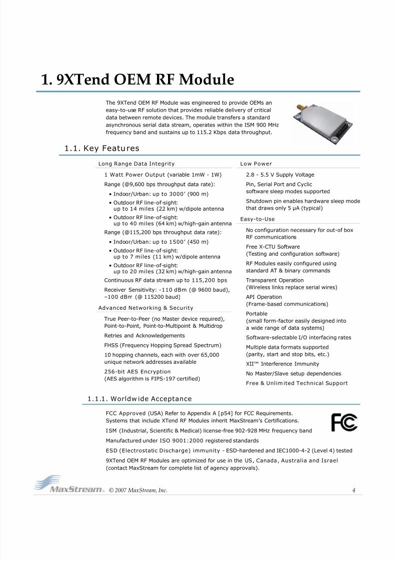
1. 9XTend OEM RF Module
The 9XTend OEM RF Module was engineered to provide OEMs an
easy-to-use RF solution that provides reliable delivery of critical
data between remote devices. The module transfers a standard
asynchronous serial data stream, operates within the ISM 900 MHz
frequency band and sustains up to 115.2 Kbps data throughput.
1.1. Key Features
Long Range Data Integrity
1 Watt Power Output (variable 1mW - 1W)
Range (@9,600 bps throughput data rate):
• Indoor/Urban: up to 3000’ (900 m)• Outdoor RF line-of-sight:
up to 14 miles (22 km) w/dipole antenna
• Outdoor RF line-of-sight: up to 40 miles (64 km) w/high-gain antenna
Range (@115,200 bps throughput data rate):
• Indoor/Urban: up to 1500’ (450 m)
• Outdoor RF line-of-sight: up to 7 miles (11 km) w/dipole antenna
• Outdoor RF line-of-sight: up to 20 miles (32 km) w/high-gain antenna
Continuous RF data stream up to 115,200 bps
Receiver Sensitivity: -110 dBm (@ 9600 baud),
–100 dBm (@ 115200 baud)
Advanced Networking & Security
True Peer-to-Peer (no Master device required),
Point-to-Point, Point-to-Multipoint & Multidrop
Retries and Acknowledgements
FHSS (Frequency Hopping Spread Spectrum)
10 hopping channels, each with over 65,000
unique network addresses available
256-bit AES Encryption
(AES algorithm is FIPS-197 certified)
Low Power
2.8 - 5.5 V Supply Voltage
Pin, Serial Port and Cyclic
software sleep modes supported
Shutdown pin enables hardware sleep mode
that draws only 5 µA (typical)
Easy-to-Use
No configuration necessary for out-of box
RF communications
Free X-CTU Software
(Testing and configuration software)
RF Modules easily configured using
standard AT & binary commands
Transparent Operation
(Wireless links replace serial wires)
API Operation
(Frame-based communications)
Portable
(small form-factor easily designed into
a wide range of data systems)
Software-selectable I/O interfacing rates
Multiple data formats supported
(parity, start and stop bits, etc.)
XII™ Interference Immunity
No Master/Slave setup dependencies
Free & Unlim ited Technical Support
1.1.1. Worldw ide Acceptance
FCC Approved (USA) Refer to Appendix A [p54] for FCC Requirements.
Systems that include XTend RF Modules inherit MaxStream’s Certifications.
ISM (Industrial, Scientific & Medical) license-free 902-928 MHz frequency band
Manufactured under ISO 9001:2000 registered standards
ESD (Electrostatic Discharge) immunity - ESD-hardened and IEC1000-4-2 (Level 4) tested
9XTend OEM RF Modules are optimized for use in the US, Canada, Australia and Israel
(contact MaxStream for complete list of agency approvals).
8/3/2019 Product Manual Xtend Oem Rfmodule
http://slidepdf.com/reader/full/product-manual-xtend-oem-rfmodule 5/71
9XTend™ OEM RF Module ‐ Product Manual v2.x4x [2007.01.04]
© 2007
MaxStream,
Inc.
5
Chapter 1 ‐ 9XTend OEM RF Module
1.2. Specifications
* If the supply voltage for a given power setting is lower than the minimum supply voltage requirement (as shown in Table 1‐02), the TX Power Output will decrease to the highest power level setting given the current supply voltage.
** 1W Power Output is not supported when using a 3.3 supply voltage.
Table 1‐01. 9XTend‐PKG‐R OEM RF Module
9XTend 900 MHz OEM RF Module Specifications
Performance @9600 bps Throughput Data Rate @115200 bps Throughput Data Rate
Transmit Power Output(software selectable using PL command)
1mW - 1 Watt 1mW - 1 Watt
Indoor/Urban Range Up to 3000’ (900 m) Up to 1500’ (450 m)
Outdoor RF line-of-sight Range
Up to 14 miles (22 km) w/ dipole antennaUp to 40 miles (64 km) w/ high-gain antenna
Up to 7 miles (11 km) w/ dipole antennaUp to 20 miles (32 km) w/ high-gain antenna
Interface Data Rate(software selectable using BD command)
1200 – 230400 bps 1200 – 230400 bps
Throughput Data Rate(software selectable using BR command)
9,600 bps 115,200 bps
RF Data Rate 10,000 bps 125,000 bps
Receiver Sensitivity -110 dBm -100 dBm
Power Requirements
Receive Current 80 mA
Shutdown Mode Power Down 5 µA typical
Pin Sleep Power Down 147 µA
Idle Currents
16 sec cyclic sleep (SM=8) 0.3 - 0.8 mA
8 sec cyclic sleep (SM=7) 0.4 - 1.4 mA
4 sec cyclic sleep (SM=6) 0.6 - 2.6 mA
2 sec cyclic sleep (SM=5) 0.9 - 4.8 mA
1 sec cyclic sleep (SM=4) 1.6 - 8.7 mA
Networking & Security
Frequency 902-928 MHz
Spread Spectrum FHSS (Frequency Hopping Spread Spectrum)
Modulation FSK (Frequency Shift Keying)
Supported Network Topologies Peer-to-Peer (“Master/Slave” relationship not required), Point-to-Point, Point-to-Multipoint
Channel Capacity 10 hop sequences share 50 frequencies
Encryption 256-bit AES Encryption – Refer to the KY Command [p29] to implement
Physical Properties
RF Module Board Size 1.44” x 2.38” x 0.20” (3.65 cm x 6.05 cm x 0.51 cm)Weight 0.64 oz. (18 g)
Connector 20-pin
Operating Temperature -40 to 85º C (industrial)
Antenna
Connector Options RPSMA (Reverse-polarity SMA) or MMCX
Impedance 50 ohms unbalanced
Certifications (partial list)
FCC Part 15.247 OUR-9XTEND
Industry Canada (IC) 4214A-9XTEND
Table 1‐02. XTend OEM RF Module Specifications ‐ Relative to user‐selected TX Power Output
Power Requirements (Supply voltage and TX currents relative to each TX Power Output option)Transmit Power Output 1 mW 10 mW 100 mW 500 mW * 1 W *
Supply Voltage 2.8 - 5.5 VDC 3.0 - 5.5 VDC 4.75 - 5.5 VDC
Transmit Current (5 V) typical 110 mA 140 mA 270 mA 500 mA 730 mA
Transmit Current (3.3 V) typical 90 mA 110 mA 260 mA 600 mA **
8/3/2019 Product Manual Xtend Oem Rfmodule
http://slidepdf.com/reader/full/product-manual-xtend-oem-rfmodule 6/71
9XTend™ OEM RF Module ‐ Product Manual v2.x4x [2007.01.04]
© 2007
MaxStream,
Inc.
6
Chapter 1 ‐ 9XTend OEM RF Module
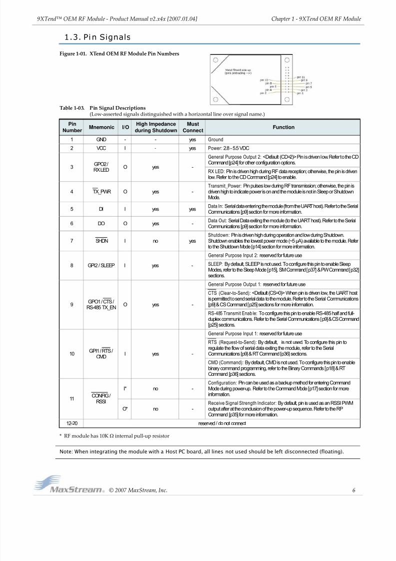
1.3. Pin Signals
Figure 1‐01. XTend OEM RF Module Pin Numbers
* RF module has 10K Ω internal pull‐up resistor
Note: When integrating the module with a Host PC board, all lines not used should be left disconnected (floating).
Table 1‐03. Pin Signal Descriptions (Low‐asserted signals distinguished with a horizontal line over signal name.)
Pin
NumberMnemonic I/O
High Impedance
during Shutdown
Must
ConnectFunction
1 GND - - yes Ground
2 VCC I - yes Power: 2.8 - 5.5 VDC
3GPO2 /RX LED
O yes -
General Purpose Output 2: <Default (CD=2)> Pin is driven low. Refer to the CDCommand[p24] for other configuration options.
RX LED: Pin is driven high during RF data reception; otherwise, the pin is drivenlow. Refer to the CD Command [p24] to enable.
4 TX_PWR O yes -Transmit_Power: Pin pulses low during RF transmission; otherwise, the pin isdriven high to indicate power is on and the module is not in Sleep or Shutdown
Mode.
5 DI I yes yesData In: Serial data entering the module (from the UART host). Refer to the SerialCommunications [p9] section for more information.
6 DO O yes -Data Out: Serial Data exiting the module (to the UART host). Refer to the SerialCommunications [p9] section for more information.
7 SHDN I no yesShutdown: Pin is driven high during operation and low during Shutdown.Shutdown enables the lowest power mode (~5 µA) available to the module. Refer to the Shutdown Mode [p14] section for more information.
8 GPI2 / SLEEP I yes -
General Purpose Input 2: reserved for future use
SLEEP: By default, SLEEP is not used. To configure this pin to enable SleepModes, refer to the Sleep Mode [p15], SM Command [p37] & PW Command [p32]sections.
9GPO1 / CTS /
RS-485 TX_ENO yes -
General Purpose Output 1: reserved for future use
CTS (Clear-to-Send): <Default (CS=0)> When pin is driven low, the UART hostis permitted to send serial data to the module. Refer to the Serial Communications[p9] & CS Command [p25] sections for more information.
RS-485 Transmit Enab le: To configure this pin to enable RS-485 half and full-duplex communications. Refer to the Serial Communications [p9] & CS Command[p25] sections.
10GPI1 / RTS /
CMDI yes -
General Purpose Input 1: reserved for future use
RTS (Request-to-Send): By default, is not used. To configure this pin toregulate the flow of serial data exiting the module, refer to the SerialCommunications [p9] & RT Command [p36] sections.
CMD (Command): By default, CMD is not used. To configure this pin to enablebinary command programming, refer to the Binary Commands [p18] & RTCommand [p36] sections.
11CONFIG /
RSSI
I* no -Configuration: Pin can be used as a backup method for entering CommandMode during power-up. Refer to the Command Mode [p17] section for more
information.
O* no -Receive Signal Strength Indicator: By default, pin is used as an RSSI PWMoutput after at the conclusion of the power-up sequence. Refer to the RPCommand [p35] for more information.
12-20 reserved / do not connect
8/3/2019 Product Manual Xtend Oem Rfmodule
http://slidepdf.com/reader/full/product-manual-xtend-oem-rfmodule 7/71
9XTend™ OEM RF Module ‐ Product Manual v2.x4x [2007.01.04]
© 2007
MaxStream,
Inc.
7
Chapter 1 ‐ 9XTend OEM RF Module
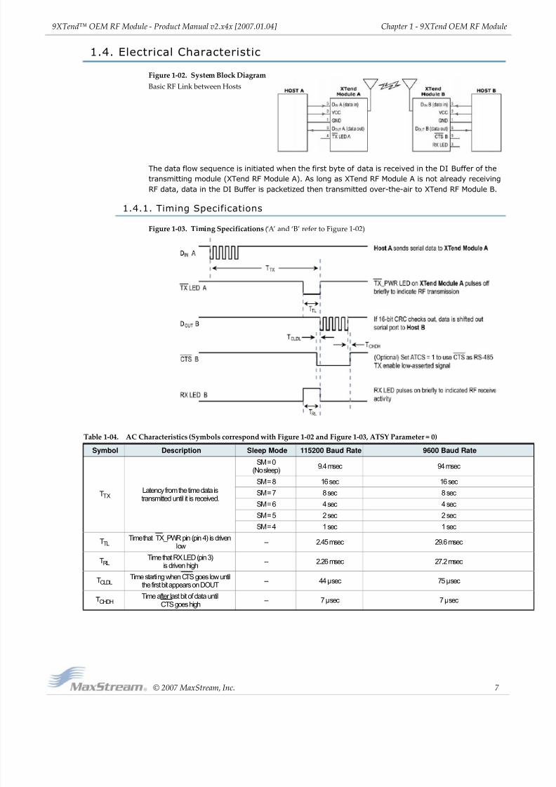
1.4. Electrical Characteristic
Figure 1‐02. System Block Diagram
Basic RF Link between Hosts
The data flow sequence is initiated when the first byte of data is received in the DI Buffer of the
transmitting module (XTend RF Module A). As long as XTend RF Module A is not already receiving
RF data, data in the DI Buffer is packetized then transmitted over-the-air to XTend RF Module B.
1.4.1. Timing Specifications
Figure 1‐03. Timing Specifications (‘A’ and ‘B’ refer to Figure 1‐02)
Table 1‐04. AC Characteristics (Symbols correspond with Figure 1‐02 and Figure 1‐03, ATSY Parameter = 0)
Symbol Description Sleep Mode 115200 Baud Rate 9600 Baud Rate
TTXLatency from the time data istransmitted until it is received.
SM = 0(No sleep)
9.4 msec 94 msec
SM = 8 16 sec 16 sec
SM = 7 8 sec 8 sec
SM = 6 4 sec 4 sec
SM = 5 2 sec 2 sec
SM = 4 1 sec 1 sec
TTLTime that TX_PWR pin (pin 4) is driven
low-- 2.45 msec 29.6 msec
TRLTime that RX LED (pin 3)
is driven high-- 2.26 msec 27.2 msec
TCLDLTime starting when CTS goes low until
the first bit appears on DOUT-- 44 µsec 75 µsec
TCHDHTime after last bit of data until
CTS goes high-- 7 µsec 7 µsec
8/3/2019 Product Manual Xtend Oem Rfmodule
http://slidepdf.com/reader/full/product-manual-xtend-oem-rfmodule 8/71
9XTend™ OEM RF Module ‐ Product Manual v2.x4x [2007.01.04]
© 2007
MaxStream,
Inc.
8
Chapter 1 ‐ 9XTend OEM RF Module
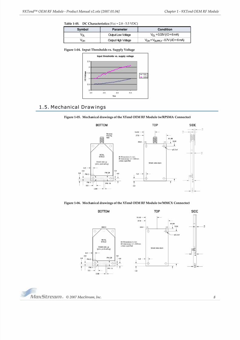
Figure 1‐04. Input Thresholds vs. Supply Voltage
1.5. Mechanical Draw ings
Figure 1‐05. Mechanical drawings of the XTend OEM RF Module (w/RPSMA Connector)
Figure 1‐06. Mechanical drawings of the XTend OEM RF Module (w/MMCX Connector)
Table 1‐05. DC Characteristics (Vcc = 2.8 ‐ 5.5 VDC)
Symbol Parameter Condition
VOL Output Low Voltage VOL = 0.33V (IO = 6 mA)
VOH Output High Voltage VOH= VSUPPLY - 0.7V (-IO = 6 mA)
Input thresholds vs. supply voltage
0
0.5
1
1.5
2
2.5
2.5 3.5 4.5 5.5
Vcc
I / O V
o l t a g e
V(IL)
V(IH)
8/3/2019 Product Manual Xtend Oem Rfmodule
http://slidepdf.com/reader/full/product-manual-xtend-oem-rfmodule 9/71
© 2007
MaxStream,
Inc.
9
2. RF Module Operation
WARNING: When operating at 1 Watt power output, observe a minimum separation distance of 2' (0.6m) between
modules. Transmitting in close proximity of other modules can damage module front ends.
2.1. Serial Communications
The XTend OEM RF Modules interface to a host device through a TTL-level asynchronous serial
port. Through its serial port, the module can communicate with any UART voltage compatible
device or through a level translator to any serial device (For example: RS-232/485/422 or USB
interface board).
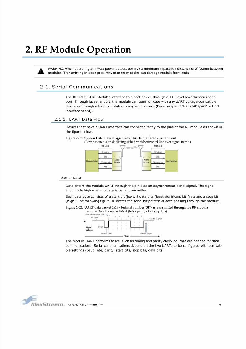
2.1.1. UART Data Flow
Devices that have a UART interface can connect directly to the pins of the RF module as shown in
the figure below.
Figure 2‐01. System Data Flow Diagram in a UART‐interfaced environment (Low‐asserted signals distinguished with horizontal line over signal name.)
Serial Data
Data enters the module UART through the pin 5 as an asynchronous serial signal. The signal
should idle high when no data is being transmitted.
Each data byte consists of a start bit (low), 8 data bits (least significant bit first) and a stop bit
(high). The following figure illustrates the serial bit pattern of data passing through the module.
Figure 2‐02. UART data packet 0x1F (decimal number ʺ31ʺ) as transmitted through the RF module Example Data Format is 8‐N‐1 (bits ‐ parity ‐ # of stop bits)
The module UART performs tasks, such as timing and parity checking, that are needed for data
communications. Serial communications depend on the two UARTs to be configured with compati-
ble settings (baud rate, parity, start bits, stop bits, data bits).
8/3/2019 Product Manual Xtend Oem Rfmodule
http://slidepdf.com/reader/full/product-manual-xtend-oem-rfmodule 10/71
9XTend™ OEM RF Module ‐ Product Manual v2.x4x [2007.01.04]
© 2007
MaxStream,
Inc.
10
Chapter 2 ‐ RF Module Operation
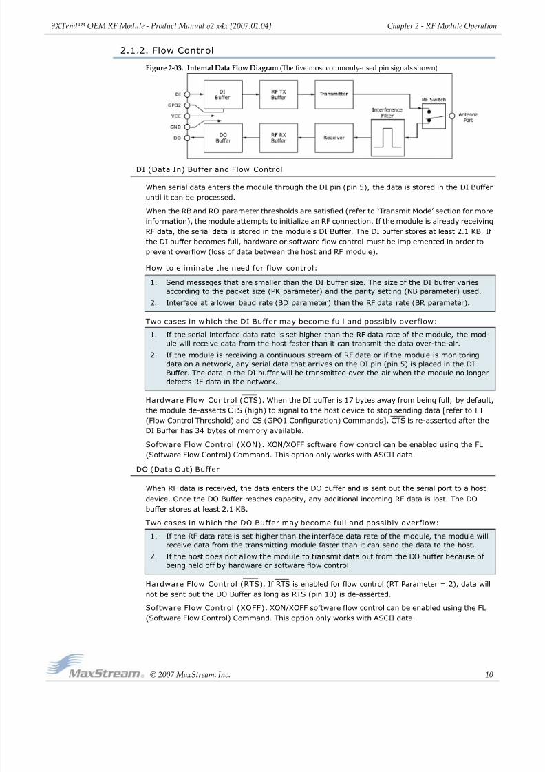
2.1.2. Flow Control
Figure 2‐03. Internal Data Flow Diagram (The five most commonly‐used pin signals shown)
DI (Data In) Buffer and Flow Control
When serial data enters the module through the DI pin (pin 5), the data is stored in the DI Buffer
until it can be processed.
When the RB and RO parameter thresholds are satisfied (refer to ‘Transmit Mode’ section for more
information), the module attempts to initialize an RF connection. If the module is already receiving
RF data, the serial data is stored in the module's DI Buffer. The DI buffer stores at least 2.1 KB. If
the DI buffer becomes full, hardware or software flow control must be implemented in order to
prevent overflow (loss of data between the host and RF module).
How to eliminate the need for flow control:
Two cases in w hich the DI Buffer may become full and possibly overflow:
Hardware Flow Control (CTS). When the DI buffer is 17 bytes away from being full; by default,
the module de-asserts CTS (high) to signal to the host device to stop sending data [refer to FT
(Flow Control Threshold) and CS (GPO1 Configuration) Commands]. CTS is re-asserted after the
DI Buffer has 34 bytes of memory available.
Software Flow Control (XON). XON/XOFF software flow control can be enabled using the FL
(Software Flow Control) Command. This option only works with ASCII data.
DO (Data Out) Buffer
When RF data is received, the data enters the DO buffer and is sent out the serial port to a host
device. Once the DO Buffer reaches capacity, any additional incoming RF data is lost. The DO
buffer stores at least 2.1 KB.
Two cases in w hich the DO Buffer may become full and possibly overflow:
Hardware Flow Control (RTS). If RTS is enabled for flow control (RT Parameter = 2), data will
not be sent out the DO Buffer as long as RTS (pin 10) is de-asserted.
Software Flow Control (XOFF). XON/XOFF software flow control can be enabled using the FL
(Software Flow Control) Command. This option only works with ASCII data.
1. Send messages that are smaller than the DI buffer size. The size of the DI buffer varies
according to the packet size (PK parameter) and the parity setting (NB parameter) used.
2. Interface at a lower baud rate (BD parameter) than the RF data rate (BR parameter).
1. If the serial interface data rate is set higher than the RF data rate of the module, the mod-
ule will receive data from the host faster than it can transmit the data over-the-air.
2. If the module is receiving a continuous stream of RF data or if the module is monitoring
data on a network, any serial data that arrives on the DI pin (pin 5) is placed in the DI
Buffer. The data in the DI buffer will be transmitted over-the-air when the module no longer
detects RF data in the network.
1. If the RF data rate is set higher than the interface data rate of the module, the module will
receive data from the transmitting module faster than it can send the data to the host.
2. If the host does not allow the module to transmit data out from the DO buffer because of
being held off by hardware or software flow control.
8/3/2019 Product Manual Xtend Oem Rfmodule
http://slidepdf.com/reader/full/product-manual-xtend-oem-rfmodule 11/71
9XTend™ OEM RF Module ‐ Product Manual v2.x4x [2007.01.04]
© 2007
MaxStream,
Inc.
11
Chapter 2 ‐ RF Module Operation
2.1.3. Transparent Operation
By default, XTend RF Modules operate in Transparent Mode. The modules act as a serial line
replacement - all UART data received through the DI pin is queued up for RF transmission. When
RF data is received, the data is sent out the DO pin.
When the RO (Packetization Timeout) parameter threshold is satisfied, the module attempts to ini-
tialize an RF transmission. If the module cannot immediately transmit (for instance, if it is already
receiving RF data), the serial data continues to be stored in the DI Buffer. Data is packetized and
sent at any RO timeout or when the maximum packet size is received.
The module operates as described above unless the Command Mode Sequence is detected. The
Command Mode Sequence consists of three copies of the command sequence character [CC
parameter] surrounded by the before and after guard times [BT & AT parameters].
If the DI buffer becomes full, hardware or software flow control must be implemented in order to
prevent overflow (loss of data between the host and module).
2.1.4. API Operation
API (Application Programming Interface) Operation is an alternative to the default Transparent
Operation. The API is frame-based and extends the level to which a host application can interact
with the networking capabilities of the module. When in API mode, all data entering and leaving
the RF module is contained in frames that define operations or events within the module.
Transmit Data Frames (received through the DI (Data In) pin) include:
• 16-bit address
Receive Data Frames (sent out the DO (Data Out) pin) include:
• Showing a received RF packet (16 bits only)
• Response to a TX (Transmit) packet
• Showing events such as hardware reset, watchdog reset, asynchronous events, etc.
The module will send data frames to the application containing status packets; as well as source,
RSSI and payload information from received data packets.
API operation option facilitates many operations such as the examples cited below:
To implement API operations, refer to ‘API Operation’ sections [p40].
-> Change destination addresses without having to enter command mode
-> Receive success/failure status of each RF packet
-> Identify the source address of each received packet

8/3/2019 Product Manual Xtend Oem Rfmodule
http://slidepdf.com/reader/full/product-manual-xtend-oem-rfmodule 12/71
9XTend™ OEM RF Module ‐ Product Manual v2.x4x [2007.01.04]
© 2007
MaxStream,
Inc.
12
Chapter 2 ‐ RF Module Operation
2.2. Modes of Operation
XTend RF Modules operate in six modes.
Figure 2‐04. XTend RF Module Modes of Operation (RF modules can only be in one mode at a time)
2.2.1. Idle Mode
When not receiving or transmitting data, the RF module is in Idle Mode. The module shifts into the
other modes of operation under the following conditions:
• Transmit Mode: Serial data is received in the DI Buffer
• Receive Mode: Valid RF data is received through the antenna
• Shutdown Mode: Shutdown condition is met
• Sleep Mode: Sleep Mode condition is met
• Command Mode: Command Mode Sequence is issued
The module automatically transitions back to Idle Mode after responding to these conditions.
2.2.2. Transmit Mode
When the first byte of serial data is received from the UART in the DI buffer, the module attempts
to shift to Transmit Mode and initiate an RF connection with other modules. After transmission is
complete, the module returns to Idle Mode.
RF transmission begins after either of the follow ing criteria is met:
Figure 2‐05. Transmit Mode Data Flow
The character timeout trigger can be
disabled by setting RO to zero. In this
case, transmission will not begin until
RB bytes have been received and are
pending for RF transmission. The RB
parameter may be set to any value
between 1 and the RF packet size [refer
to PK (Max RF Packet Size) parameter],inclusive. Note that transition to Trans-
mit Mode cannot take place during RF
reception; the RF reception must com-
plete before the radio can transition into
Transmit Mode.
If RB or RO conditions are met, the
module initializes a communications channel. Serial data in the DI buffer is grouped into RF pack-
ets (up to 2048 bytes in each packet, refer to PK Command), converted to RF data and is transmit-
ted over-the-air until the DI buffer is empty.
1. RB bytes have been received by the UART and are pending for RF transmission.
[Refer to the RB (Packetization Threshold) Command]
2. At least one character has been received by the UART and is pending for RF transmission;
and RO character times of silence been observed on the UART.
[Refer to the RO (Packetization Timeout) Command]
8/3/2019 Product Manual Xtend Oem Rfmodule
http://slidepdf.com/reader/full/product-manual-xtend-oem-rfmodule 13/71
9XTend™ OEM RF Module ‐ Product Manual v2.x4x [2007.01.04]
© 2007
MaxStream,
Inc.
13
Chapter 2 ‐ RF Module Operation
Channel initialization is the process of sending an RF initializer that synchronizes receiving mod-
ules with the transmitting module. During channel initialization, incoming serial data accumulates
in the DI buffer.
RF data, which includes the payload data, follows the RF initializer. The payload includes up to the
maximum packet size (PK Command) bytes. As the TX module nears the end of the transmission,
it inspects the DI buffer to see if more data exists to be transmitted. This could be the case if more
than PK bytes were originally pending in the DI buffer or if more bytes arrived from the UART after
the transmission began. If more data is pending, the transmitting module assembles a subsequent
packet for transmission.
Refer to the ‘RF Communication Modes’ section to view state diagrams that illustrate channel ini-
tialization and the sequence of events that follow.
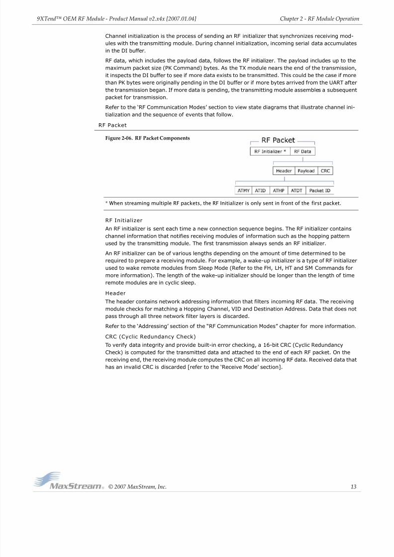
RF Packet
Figure 2‐06. RF Packet Components
* When streaming multiple RF packets, the RF Initializer is only sent in front of the first packet.
RF Initializer
An RF initializer is sent each time a new connection sequence begins. The RF initializer contains
channel information that notifies receiving modules of information such as the hopping pattern
used by the transmitting module. The first transmission always sends an RF initializer.
An RF initializer can be of various lengths depending on the amount of time determined to be
required to prepare a receiving module. For example, a wake-up initializer is a type of RF initializer
used to wake remote modules from Sleep Mode (Refer to the FH, LH, HT and SM Commands for
more information). The length of the wake-up initializer should be longer than the length of time
remote modules are in cyclic sleep.
Header
The header contains network addressing information that filters incoming RF data. The receiving
module checks for matching a Hopping Channel, VID and Destination Address. Data that does not
pass through all three network filter layers is discarded.
Refer to the ‘Addressing’ section of the “RF Communication Modes” chapter for more information.
CRC (Cyclic Redundancy Check)
To verify data integrity and provide built-in error checking, a 16-bit CRC (Cyclic Redundancy
Check) is computed for the transmitted data and attached to the end of each RF packet. On the
receiving end, the receiving module computes the CRC on all incoming RF data. Received data that
has an invalid CRC is discarded [refer to the ‘Receive Mode’ section].

8/3/2019 Product Manual Xtend Oem Rfmodule
http://slidepdf.com/reader/full/product-manual-xtend-oem-rfmodule 14/71
9XTend™ OEM RF Module ‐ Product Manual v2.x4x [2007.01.04]
© 2007
MaxStream,
Inc.
14
Chapter 2 ‐ RF Module Operation
2.2.3. Receive Mode
If a module detects RF data while operating in Idle Mode, the module transitions to Receive Mode
to start receiving RF packets. Once a packet is received, the module checks the CRC (cyclic redun-
dancy check) to ensure that the data was transmitted without error. If the CRC data bits on the
incoming packet are invalid, the packet is discarded. If the CRC is valid, the packet proceeds to the
DO Buffer.
Figure 2‐07. Receive Mode Data Flow
* Refer
to
the
‘Address
Recognition’
sec
‐
tion for more information regarding address recognition.
The module returns to Idle Mode
when valid RF data is no longer
detected or after an error is
detected in the received RF data. If
serial data is stored in the DI
buffer while the module is in
Receive Mode, the serial data will
be transmitted after the module is
finished receiving data and returnsto Idle Mode.
2.2.4. Shutdown Mode
Hardware Sleep
For applications where power consumption must be kept to a minimum during idle periods, Shut-
down Mode offers the lowest power mode available to the module.
When the SHDN pin (pin 7) is driven low, the module is forced into shutdown mode. Any commu-
nication in progress (transmit or receive) will be halted and any buffered data will be lost. For anyother mode of operation, SHDN must be driven or pulled high. While in shutdown mode, the mod-
ule's VCC pin draws 5 µA (typical).
Immediately after the SHDN pin changes state from low to high, the module resets. After reset,
there is a delay that must be observed. Delay time is <100ms.
While SHDN pin is driven low, the following pins are set to high impedance by the module: DCD,
TX_PWR, RX LED, DO and CTS (See pin signal descriptions, p6). The SHDN line (also used for
RSSI indication) is driven low during shutdown.
The following input pins may continue to be driven by external circuitry when in shutdown mode:
PIN_PWR_DWN, RTS, DI and SHDN.
Note: Because the DO pin also goes high impedance, if the XTend RF Module is connected to a pro-
cessor, the UART receive pin could be floating. A weak pull-up should be placed between the moduleand the microcontroller so that data is not interpreted as being transmitted to the microprocessor.
8/3/2019 Product Manual Xtend Oem Rfmodule
http://slidepdf.com/reader/full/product-manual-xtend-oem-rfmodule 15/71
9XTend™ OEM RF Module ‐ Product Manual v2.x4x [2007.01.04]
© 2007
MaxStream,
Inc.
15
Chapter 2 ‐ RF Module Operation
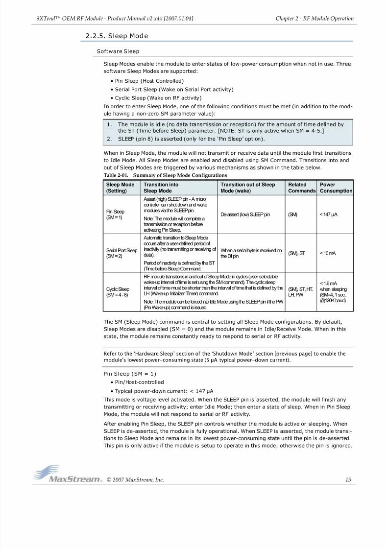
2.2.5. Sleep Mode
Software Sleep
Sleep Modes enable the module to enter states of low-power consumption when not in use. Three
software Sleep Modes are supported:
• Pin Sleep (Host Controlled)
• Serial Port Sleep (Wake on Serial Port activity)
• Cyclic Sleep (Wake on RF activity)
In order to enter Sleep Mode, one of the following conditions must be met (in addition to the mod-
ule having a non-zero SM parameter value):
When in Sleep Mode, the module will not transmit or receive data until the module first transitions
to Idle Mode. All Sleep Modes are enabled and disabled using SM Command. Transitions into and
out of Sleep Modes are triggered by various mechanisms as shown in the table below.
The SM (Sleep Mode) command is central to setting all Sleep Mode configurations. By default,
Sleep Modes are disabled (SM = 0) and the module remains in Idle/Receive Mode. When in this
state, the module remains constantly ready to respond to serial or RF activity.
Refer to the ‘Hardware Sleep’ section of the ‘Shutdown Mode’ section [previous page] to enable the
module's lowest power-consuming state (5 µA typical power-down current).
Pin Sleep (SM = 1)
• Pin/Host-controlled• Typical power-down current: < 147 µA
This mode is voltage level activated. When the SLEEP pin is asserted, the module will finish any
transmitting or receiving activity; enter Idle Mode; then enter a state of sleep. When in Pin Sleep
Mode, the module will not respond to serial or RF activity.
After enabling Pin Sleep, the SLEEP pin controls whether the module is active or sleeping. When
SLEEP is de-asserted, the module is fully operational. When SLEEP is asserted, the module transi-
tions to Sleep Mode and remains in its lowest power-consuming state until the pin is de-asserted.
This pin is only active if the module is setup to operate in this mode; otherwise the pin is ignored.
1. The module is idle (no data transmission or reception) for the amount of time defined by
the ST (Time before Sleep) parameter. [NOTE: ST is only active when SM = 4-5.]
2. SLEEP (pin 8) is asserted (only for the ‘Pin Sleep’ option).
Table 2‐01. Summary of Sleep Mode Configurations
Sleep Mode
(Setting)
Transition into
Sleep Mode
Transition out of Sleep
Mode (wake)
Related
Commands
Power
Consumption
Pin Sleep (SM = 1)
Assert (high) SLEEP pin - A microcontroller can shut down and wakemodules via the SLEEP pin.
Note: The module will complete atransmission or reception beforeactivating Pin Sleep.
De-assert (low) SLEEP pin (SM) < 147 µA
Serial Port Sleep (SM = 2)
Automatic transition to Sleep Modeoccurs after a user-defined period of inactivity (no transmitting or receiving of data).
Period of inactivity is defined by the ST(Time before Sleep) Command.
When a serial byte is received onthe DI pin
(SM), ST < 10 mA
Cyclic Sleep (SM = 4 - 8)
RF module transitions in and out of Sleep Mode in cycles (user-selectablewake-up interval of time is set using the SM command). The cyclic sleep
interval of time must be shorter than the interval of time that is defined by theLH (Wake-up Initializer TImer) command.
Note: The module can be forced into Idle Mode using the SLEEP pin if the PW(Pin Wake-up) command is issued.
(SM), ST, HT,LH, PW
< 1.6 mA
when sleeping(SM=4, 1 sec.,@120K baud)

8/3/2019 Product Manual Xtend Oem Rfmodule
http://slidepdf.com/reader/full/product-manual-xtend-oem-rfmodule 16/71
9XTend™ OEM RF Module ‐ Product Manual v2.x4x [2007.01.04]
© 2007
MaxStream,
Inc.
16
Chapter 2 ‐ RF Module Operation
Once in Pin Sleep, CTS (GPO1) is de-asserted (high), indicating that data should not be sent to the
module. The PWR pin is also de-asserted (low) when the module is in Pin Sleep Mode.
Note: The module will complete a transmission or reception before activating Pin Sleep.
Serial Port Sleep (SM = 2)
• Wake on serial port activity
• Typical power-down current: < 10 mA
Serial Port Sleep is a Sleep Mode in which the module runs in a low power state until serial data is
detected on the DI pin.
The period of time the module sleeps is determined by ST (Time before Sleep) Command. Once a
character is received through the DI pin, the module returns to Idle Mode and is fully operational.
Cyclic Sleep (SM = 4-8)
• Typical Power-down Current: < 1.6 mA (when asleep)
Cyclic Sleep Modes allow modules to periodically wake and check for RF data. The module wakes
according to the times designated by the Cyclic sleep settings. If the module detects a wake-up
initializer during the time it is awake, the module synchronizes with the transmitting module and
receives data after the wake-up initializer runs its duration. Otherwise, the module returns to
Sleep Mode and continues to cycle in and out of activity until a wake-up initializer is detected.
While the module is in Cyclic Sleep Mode, CTS (GPO1) is de-asserted (high) to indicate that datashould not be sent to the module. When the module awakens to listen for data, GPO1 is asserted
and any data received on the DI Pin is transmitted. The PWR pin is also de-asserted (low) when
the module is in Cyclic Sleep Mode.
The module remains in Sleep Mode for a user-defined period of time ranging from 0.5 seconds to
16 seconds (SM parameters 4 through 8). After this interval of time, the module returns to Idle
Mode and listens for a valid data packet for 100 ms. If the module does not detect valid data (on
any frequency), the module returns to Sleep Mode. If valid data is detected, the module transi-
tions into Receive Mode and receives the incoming RF packets. The module then returns to Sleep
Mode after a period of inactivity determined by the ST "Time before Sleep" parameter.
The module can also be configured to wake from cyclic sleep when the SLEEP pin is de-asserted.
To configure a module to operate in this manner, PW (Pin Wake-up) Command must be issued.
Once the SLEEP pin is de-asserted, the module is forced into Idle Mode and can begin transmitting
or receiving data. It remains active until data is no longer detected for the period of time specifiedby the ST Command, at which point it resumes its low-power cyclic state.
Cyclic Scanning. Each RF transmission consists of an RF Initializer and payload. The RF initializer
contains initialization information and all receiving modules must wake during the wake-up initial-
izer portion of data transmission in order to be synchronized with the transmitting module and
receive the data.
The cyclic interval time defined by the SM (Sleep Mode) command must be shorter than the intervaltime defined by LH (Wake-up Initializer Timer) command.
Figure 2‐08. Correct Configuration (LH > SM): The length of the wake‐up initializer exceeds the time interval of Cyclic Sleep. The receiver is guaranteed to detect the wake‐up initializer and receive the accompanying payload data.

8/3/2019 Product Manual Xtend Oem Rfmodule
http://slidepdf.com/reader/full/product-manual-xtend-oem-rfmodule 17/71
9XTend™ OEM RF Module ‐ Product Manual v2.x4x [2007.01.04]
© 2007
MaxStream,
Inc.
17
Chapter 2 ‐ RF Module Operation
2.2.6. Command Mode
To modify or read module parameters, the module must first enter into Command Mode (state in
which incoming characters are interpreted as commands). Two command types are supported:
• AT Commands
• Binary Commands
For modified parameter values to persist in the module registry, changes must be saved to non-
volatile memory using the WR (Write) command. Otherwise, parameters are restored to previously
saved values when the module is powered off and then on again.
AT Command Mode
To Enter AT Command Mode:
Default AT Command Mode Sequence (for transition to Command Mode):
• No characters sent for one second [refer to the BT (Guard Time Before) Command]
• Input three plus characters (“+++”) within one second [refer to the CC (Command Sequence Character) Command.]
• No characters sent for one second [refer to the AT (Guard Time After) Command.]
All of the parameter values in the sequence can be modified to reflect user preferences.
To Send AT Commands:
Figure 2‐09. Syntax for sending AT Commands
To read a parameter value stored in the module register, leave the parameter field blank.
The preceding example would change the module’s Destination Address to "0x1F". To store the
new value to non-volatile (long term) memory, the Write (ATWR) command must subsequently be
sent before powering off the module.
System Response. When a command is sent to the module, the module will parse and execute
the command. Upon successful execution of a command, the module returns an “OK” message. If
execution of a command results in an error, the module returns an “ERROR” message.
To Exit AT Command Mode:
For an example of programming the RF module using AT Commands and descriptions of each config-
urable parameter, refer to the "RF Module Configuration" chapter [p19].
1. Send the 3-character command sequence "+++" and observe guard times before and after
the command characters. [refer to ‘Default AT Command Mode Sequence’ below.] The ‘Ter-
minal’ tab (or other serial communications software) of the X-CTU Software can be used to
enter the sequence.
[OR]
2. Assert (low) the CONFIG pin and turn the power going to the module off and back on (or
pulse the SHDN pin).
[If the module is mounted to a MaxStream RS-232/485 Interface Board, the result can be
achieved by pressing the configuration switch down for 2 seconds.]
Send AT commands and parameters using the syntax shown below.
1. If no valid AT Commands are received within the time specified by CT (Command Mode
Timeout) Command, the module automatically returns to Idle Mode.
[OR]
2. Send ATCN (Exit Command Mode) Command.
8/3/2019 Product Manual Xtend Oem Rfmodule
http://slidepdf.com/reader/full/product-manual-xtend-oem-rfmodule 18/71
9XTend™ OEM RF Module ‐ Product Manual v2.x4x [2007.01.04]
© 2007
MaxStream,
Inc.
18
Chapter 2 ‐ RF Module Operation
Binary Command Mode
Sending and receiving parameter values using binary commands is the fastest way to change
operating parameters of the module. Binary commands are used most often to sample signal
strength [refer to DB (Received Signal Strength) parameter] and/or error counts; or to change
module addresses and channels for polling systems when a quick response is necessary. Since the
sending and receiving of parameter values takes place through the same serial data path as 'live'
data (received RF payload), interference between the two types of data can be a concern.
Common questions about using binary commands:• What are the implications of asserting CMD while live data is being sent or received?
• After sending serial data, is there a minimum time delay before CMD can be asserted?
• Is a time delay required after CMD is de-asserted before payload data can be sent?
• How does one discern between live data and data received in response to a command?
The CMD pin (pin 10) must be asserted in order to send binary commands to the module. The
CMD pin can be asserted to recognize binary commands anytime during the transmission or recep-
tion of data. The status of the CMD signal is only checked at the end of the stop bit as the byte is
shifted into the serial port. The application does not allow control over when data is received,
except by waiting for dead time between bursts of communication.
If the command is sent in the middle of a stream of payload data to be transmitted, the command
will essentially be executed in the order it is received. If the module is continuously receiving data,
the radio will wait for a break in the received data before executing the command. The CTS signalwill frame the response coming from the binary command request [refer to figure below].
A minimum time delay of 100 µs (after the stop bit of the command byte has been sent) must be
observed before the CMD pin can be de-asserted. The command executes after all parameters
associated with the command have been sent. If all parameters are not received within 0.5 sec-
onds, the module returns to Idle Mode.
Note: When parameters are sent, they are two bytes long with the least significant byte sent first.
Binary commands that return one parameter byte must be written with two parameter bytes.
Commands can be queried for their current value by sending the command logically ORed (bit-
wise) with the value 0x80 (hexadecimal) with CMD asserted. When the binary value is sent (with
no parameters), the current value of the command parameter is sent back through the DO pin.
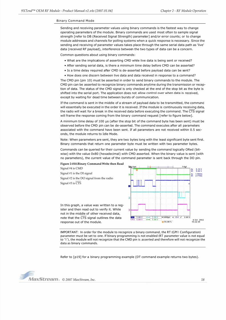
Figure 2‐010.Binary Command Write then Read
Signal #4 is CMD
Signal #1 is the DI signal
Signal #2 is the DO signal from the radio
Signal #3 is CTS
In this graph, a value was written to a reg-
ister and then read out to verify it. While
not in the middle of other received data,
note that the CTS signal outlines the data
response out of the module.
IMPORTANT: In order for the module to recognize a binary command, the RT (GPI1 Configuration)
parameter must be set to one. If binary programming is not enabled (RT parameter value is not equal
to ‘1’), the module will not recognize that the CMD pin is asserted and therefore will not recognize the
data as binary commands.
Refer to [p19] for a binary programming example (DT command example returns two bytes).
8/3/2019 Product Manual Xtend Oem Rfmodule
http://slidepdf.com/reader/full/product-manual-xtend-oem-rfmodule 19/71
© 2007
MaxStream,
Inc.
19
3. RF Module Configuration
3.1. Programming Examples
Refer to the ‘Command Mode’ section [p17] for information regarding entrance into Command
Mode, sending AT commands and exiting Command Mode. Refer to the ‘X-CTU’ section [ p69] of
the ‘Development Guide’ for more information regarding MaxStream’s configuration software.
3.1.1. AT Commands
To Send AT Commands (Using the ‘Terminal’ tab of the X-CTU Software)
Note: When using X-CTU Software to program a module, PC com port settings must match the baud
(interface data rate), parity & stop bits parameter settings of the module. Use the 'Com Port Setup'
section of the “PC Settings” tab to configure PC com port settings to match those of the module.
3.1.2. Binary Commands
To Send Binary Commands:
Note: CTS (pin 9) is high when a command is being executed. Hardware flow control must be disabled
as CTS will hold off parameter bytes.
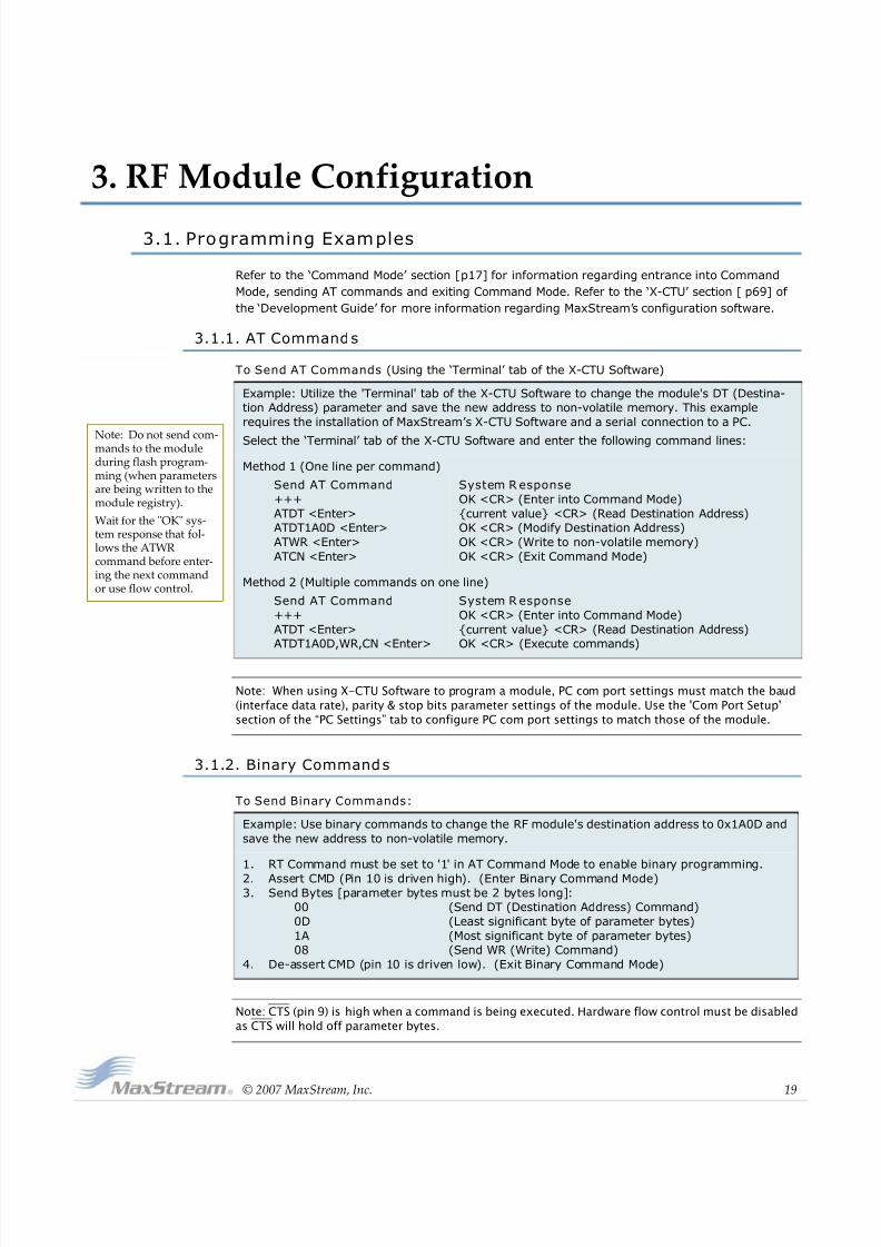
Example: Utilize the 'Terminal' tab of the X-CTU Software to change the module's DT (Destina-
tion Address) parameter and save the new address to non-volatile memory. This example
requires the installation of MaxStream’s X-CTU Software and a serial connection to a PC.
Select the ‘Terminal’ tab of the X-CTU Software and enter the following command lines:
Method 1 (One line per command)
Send AT Command
+++
ATDT <Enter>
ATDT1A0D <Enter>
ATWR <Enter>
ATCN <Enter>
System R esponse
OK <CR> (Enter into Command Mode)
{current value} <CR> (Read Destination Address)
OK <CR> (Modify Destination Address)
OK <CR> (Write to non-volatile memory)
OK <CR> (Exit Command Mode)
Method 2 (Multiple commands on one line)
Send AT Command
+++
ATDT <Enter>
ATDT1A0D,WR,CN <Enter>
System R esponse
OK <CR> (Enter into Command Mode)
{current value} <CR> (Read Destination Address)
OK <CR> (Execute commands)
Example: Use binary commands to change the RF module's destination address to 0x1A0D and
save the new address to non-volatile memory.
1. RT Command must be set to '1' in AT Command Mode to enable binary programming.
2. Assert CMD (Pin 10 is driven high). (Enter Binary Command Mode)
3. Send Bytes [parameter bytes must be 2 bytes long]:
00 (Send DT (Destination Address) Command)
0D (Least significant byte of parameter bytes)
1A (Most significant byte of parameter bytes)
08 (Send WR (Write) Command)
4. De-assert CMD (pin 10 is driven low). (Exit Binary Command Mode)
Note: Do
not
send
com
‐
mands to the module during flash program‐
ming (when parameters are being written to the module registry).
Wait for the ʺOKʺ sys‐tem response that fol‐lows the ATWR
command before enter‐ing the next command
or use flow control.
8/3/2019 Product Manual Xtend Oem Rfmodule
http://slidepdf.com/reader/full/product-manual-xtend-oem-rfmodule 20/71
9XTend™ OEM RF Module ‐ Product Manual v2.x4x [2007.01.04]
© 2007
MaxStream,
Inc.
20
Chapter 3 ‐ RF Module Configuration
3.2. Command Reference Table
Table 3‐01. XTend Commands (The RF modules expect numerical values in hexadecimal. Hexadecimal values are designated by a “0x” prefix. Decimal equivalents are designated by a “d” suffix.)
AT
Command
Binary
CommandAT Command Name Parameter Range
Command
Category
# Bytes
Returned
Factory
Default
%V 0x3B (59d) Board Voltage 0x2CCCA - 0x5BFFA [read-only] Diagnostics 4 --
AM 0x40 (64d) Auto-set MY -- Networking & Security -- --
AP v2.x20* -- API Enable 0 - 2 Serial Interfacing 1 0
AT 0x05 (5d) Guard Time After 2 - (ATST-3) [x 100 msec] Command Mode Options 2 0x0A (10d)
BD 0x15 (21d) Interface Data Rate0 - 8 (standard rates)0x39 - 0x1C9C38 (non-standard rates)
Serial Interfacing 4 3
BR 0x39 (57d) RF Data Rate 0 - 1 RF Interfacing 1 1
BT 0x04 (4d) Guard Time Before 0 - 0xFFFF [x 100 msec] Command Mode Options 2 0x0A (10d)
CC 0x13 (19d) Command Sequence Character 0x20 - 0x7F Command Mode Options 1 0x2B ["+"] (43d)
CD 0x28 (40d) GPO2 Configuration 0 - 4 Serial Interfacing 1 2
CF -- Number Base 0 - 2 Command Mode Options 1 1
CN 0x09 (9d) Exit Command Mode -- Command Mode Options -- --
CS 0x1F (31d) GPO1 Configuration 0 - 4 Serial Interfacing 1 0
CT 0x06 (6d) Command Mode Timeout 2 - 0xFFFF [x 100 ms] Command Mode Options 2 0xC8 (200d)
DB 0x36 (54d) Received Signal Strength 0x6E - 0x28 [read-only] Diagnostics 2 --
DT 0x00 (0d) Destination Address 0 - 0xFFFF Networking & Security 2 0
E0 0x0A (10d) Echo Off -- Command Mode Options -- --
E1 0x0B (11d) Echo On -- Command Mode Options -- --
ER 0x0F (15d) Receive Error Count 0 - 0xFFFF Diagnostics 2 0
FH 0x0D (13d) Force Wake-up Initializer -- Sleep (Low Power) -- --
FL 0x07 (7d) Software Flow Control 0 - 1 Serial Interfacing 1 0
FS 0x3E (62d) Forced Sync Time 0 - 0xFFFF [x 10 msec] RF Interfacing 2 0
FT 0x24 (36d) Flow Control Threshold 0 - (DI buffer size - 0x11) [Bytes] Serial Interfacing 2 DI buffer sizeminus 0x11
GD 0x10 (16d) Receive Good Count 0 - 0xFFFF Diagnostics 2 0
HP 0x11 (17d) Hopping Channel 0 - 9 Networking & Security 1 0
HT 0x03 (3d) Time before Wake-up Initializer 0 - 0xFFFF [x 100 msec] Sleep (Low Power) 20xFFFF(65535d)
HV -- Hardware Version 0 - 0xFFFF [read-only] Diagnostics 2 --
ID 0x27 (39d) Modem VID0x11 - 0x7FFF (user-settable)0x8000 - 0xFFFF (factory-set, read-only)
Networking & Security 20x3332(13106d)
KY 0x3C (60d) AES Encryption Key 0 - (Any other 64-digit hex valid key) Networking & Security 2 0
LH 0x0C (12d) Wake-up Initializer Timer 0 - 0xFF [x 100 msec] Sleep (Low Power) 1 1
MD v2.x20* 0x31 (49d) RF Mode 0 - 6 Networking & Security 1 0
MK 0x12 (18d) Address Mask 0 - 0xFFFF Networking & Security 20xFFFF(65535d)
MT 0x3D (61d) Multi-Transmit 0 - 0xFF Networking & Security 1 0
MY 0x2A (42d) Source Address 0 - 0xFFFF Networking & Security 20xFFFF(65535d)
NB 0x23 (35d) Parity 0 - 4 Serial Interfacing 1 0
PB v2.x20* 0x45 (69d) Polling Begin Address 0 - 0xFFFF Networking & Security 2 0
PD v2.x20* 0x47 (71d) Minimum Polling Delay0 - 0xFFFF(Base: (x 1 ms), Remote: [x 10 ms])
Networking & Security 2 0
8/3/2019 Product Manual Xtend Oem Rfmodule
http://slidepdf.com/reader/full/product-manual-xtend-oem-rfmodule 21/71
9XTend™ OEM RF Module ‐ Product Manual v2.x4x [2007.01.04]
© 2007
MaxStream,
Inc.
21
Chapter 3 ‐ RF Module Configuration
* Firmware version in which command and parameter options were first supported
PE v2.x20* 0x46 (70d) Polling End Address 0 - 0xFFFF Networking & Security 2 0
PK 0x29 (41d) Maximum RF Packet Size 1 - 0x800 [Bytes] RF Interfacing 2 varies
PL 0x3A (58d) TX Power Level 0 - 4 RF Interfacing 1 4 (1 Watt)
PW 0x1D (29d) Pin Wake-up 0 - 1 Sleep (Low Power) 1 0RB 0x20 (32d) Packetization Threshold 1 - Current value of PK Serial Interfacing 2 0x800 (2048d)
RC -- Ambient Power - Single Channel 0 - 0x31 [dBm, read-only] Diagnostics 1 --
RE 0x0E (14d) Restore Defaults -- (Special) -- --
RM -- Ambient Power - All Channels No parameter - 0x7D0 Diagnostics 2 --
RN 0x19 (25d) Delay Slots 0 - 0xFF [slots] Networking & Security 1 0
RO 0x21 (33d) Packetization Timeout 0 - 0xFFFF [x UART character time] Serial Interfacing 2 3
RP 0x22 (34d) RSSI PWM Timer 0 - 0xFF [x 100 msec] Diagnostics 1 0x20 (32d)
RR 0x18 (24d) Retries 0 - 0xFF Networking & Security 1 0x0A (10d)
RT 0x16 (22d) GPI1 Configuration 0 - 2 Serial Interfacing 1 0
SB 0x37 (55d) Stop Bits 0 - 1 Serial Interfacing 1 0
SH 0x25 (37d) Serial Number High 0 - 0xFFFF [read-only] Diagnostics 2 varies
SL 0x26 (38d) Serial Number Low 0 - 0xFFFF [read-only] Diagnostics 2 varies
SM 0x01 (1d) Sleep Mode 0 - 8 (3 is reserved) Sleep (Low Power) 1 0
ST 0x02 (2d) Time before Sleep (ATAT+3) - 0x7FFF [x 100 msec] Sleep (Low Power) 2 0x64 (100d)
TP 0x38 (56d) Board Temperature 0 - 0x7F [read-only] Diagnostics 1 --
TR 0x1B (27d) Delivery Failure Count 0 - 0xFFFF [read-only] Diagnostics 2 0
TT 0x1A (26d) Streaming Limit 0 - 0xFFFF [0 = disabled] Networking & Security 2 0
TX 0x3F (63d) Transmit Only 0 - 1 RF Interfacing 1 0
VL -- Firmware Version - verbose Returns string Diagnostics -- --
VR 0x14 (20d) Firmware Version 0 - 0xFFFF [read-only] Diagnostics 2 --
WA -- Active Warning Numbers Returns string Diagnostics -- --WN -- Warning Data Returns string Diagnostics -- --
WR 0x08 (8d) Write -- (Special) -- --
WS -- Sticky Warning Numbers Returns string Diagnostics -- --
Table 3‐01. XTend Commands (The RF modules expect numerical values in hexadecimal. Hexadecimal values are designated by a “0x” prefix. Decimal equivalents are designated by a “d” suffix.)
AT
Command
Binary
CommandAT Command Name Parameter Range
Command
Category
# Bytes
Returned
Factory
Default
8/3/2019 Product Manual Xtend Oem Rfmodule
http://slidepdf.com/reader/full/product-manual-xtend-oem-rfmodule 22/71
9XTend™ OEM RF Module ‐ Product Manual v2.x4x [2007.01.04]
© 2007
MaxStream,
Inc.
22
Chapter 3 ‐ RF Module Configuration
3.3. Command Descriptions
Commands in this section are listed alphabetically. Command categories are designated between
the "< >" symbols that follow each command title. By default, XTend RF Modules expect numerical
values in hexadecimal since the default value of the CF (Number Base) Parameter is '1'. Hexadec-
imal values are designated by the "0x" prefix and decimal values by the "d" suffix.
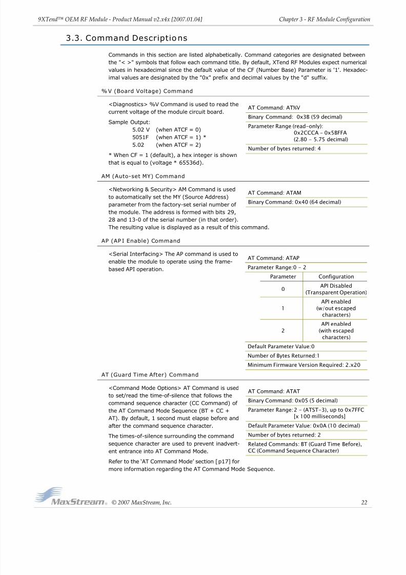
%V (Board Voltage) Command
<Diagnostics> %V Command is used to read the
current voltage of the module circuit board.
Sample Output:
5.02 V (when ATCF = 0)
5051F (when ATCF = 1) *
5.02 (when ATCF = 2)
* When CF = 1 (default), a hex integer is shown
that is equal to (voltage * 65536d).
AM (Auto-set MY) Command
<Networking & Security> AM Command is used
to automatically set the MY (Source Address)
parameter from the factory-set serial number of
the module. The address is formed with bits 29,
28 and 13-0 of the serial number (in that order).
The resulting value is displayed as a result of this command.
AP (AP I Enable) Command
<Serial Interfacing> The AP command is used to
enable the module to operate using the frame-
based API operation.
AT (Guard Time After) Command
<Command Mode Options> AT Command is used
to set/read the time-of-silence that follows the
command sequence character (CC Command) of the AT Command Mode Sequence (BT + CC +
AT). By default, 1 second must elapse before and
after the command sequence character.
The times-of-silence surrounding the command
sequence character are used to prevent inadvert-
ent entrance into AT Command Mode.
Refer to the ‘AT Command Mode’ section [p17] for
more information regarding the AT Command Mode Sequence.
AT Command: AT%V
Binary Command: 0x3B (59 decimal)
Parameter Range (read-only):0x2CCCA - 0x5BFFA
(2.80 - 5.75 decimal)
Number of bytes returned: 4
AT Command: ATAM
Binary Command: 0x40 (64 decimal)
AT Command: ATAP
Parameter Range:0 - 2
Parameter Configuration
0API Disabled
(Transparent Operation)
1API enabled
(w/out escapedcharacters)
2
API enabled
(with escaped
characters)
Default Parameter Value:0
Number of Bytes Returned:1
Minimum Firmware Version Required: 2.x20
AT Command: ATAT
Binary Command: 0x05 (5 decimal)Parameter Range:2 - (ATST-3), up to 0x7FFC
[x 100 milliseconds]
Default Parameter Value: 0x0A (10 decimal)
Number of bytes returned: 2
Related Commands: BT (Guard Time Before),CC (Command Sequence Character)

8/3/2019 Product Manual Xtend Oem Rfmodule
http://slidepdf.com/reader/full/product-manual-xtend-oem-rfmodule 23/71
9XTend™ OEM RF Module ‐ Product Manual v2.x4x [2007.01.04]
© 2007
MaxStream,
Inc.
23
Chapter 3 ‐ RF Module Configuration
BD (Interface Data Rate) Command
<Serial Interfacing> The BD command is used to
set and read the serial interface data rate (baud
rate) used between the RF module and host. This
parameter determines the rate at which serial
data is sent to the module from the host. Modified
interface data rates do not take effect until the CN
(Exit AT Command Mode) command is issued and
the system returns the 'OK' response.
When parameters 0-8 are sent to the module, the
respective interface data rates are used (as
shown in the table on the right).
The RF data rate is not affected by the BD param-
eter. If the interface data rate is set higher than
the RF data rate, a flow control configuration may
need to be implemented.
The range between standard and non-standard
baud rates (0x09 - 0x38) is invalid.
Non-standard Interface Data Rates:
Any value above 0x38 will be interpreted as an
actual baud rate. When a value above 0x38 is
sent, the closest interface data rate represented
by the number is stored in the BD register. For example, a rate of 19200 bps can be set by sending
the following command line "ATBD4B00". NOTE: When using MaxStream’s X-CTU Software, non-
standard interface data rates can only be set and read using the X-CTU ‘Terminal’ tab. Non-stan-
dard rates are not accessible through the ‘Modem Configuration’ tab.
When the BD command is sent with a non-standard interface data rate, the UART will adjust to
accommodate the requested interface rate. In most cases, the clock resolution will cause the
stored BD parameter to vary from the parameter that was sent (refer to the table below). Reading
the BD command (send "ATBD" command without an associated parameter value) will return the
value actually stored in the module’s BD register.
BR (RF Data Rate) Command
<RF Interfacing> The BR command is used to set
and read the RF data rate (rate that RF data is
transmitted over-the-air) of the module.
Parameters Sent Versus Parameters Stored
BD Parameter Sent (HEX) Interface Data Rate (bps) BD Parameter Stored (HEX)0 1200 0
4 19,200 4
7 115,200 7
12C 300 12B
1C200 115,200 1B207
AT Command: ATBD
Binary Command: 0x15 (21 decimal)
Parameter Ranges: 0 - 8 (standard rates)
0x39 - 0x1C9C38 (non-standard rates)
Parameter Configuration (bps)
0 12001 2400
2 4800
3 9600
4 19200
5 38400
6 57600
7 115200
8 230400
Default Parameter Value: 3
Non-standard baud rates supported as of
firmware v2.x20
Number of bytes returned: 4
AT Command: ATBR
Binary Command: 0x39 (57 decimal)
Parameter Range:0 - 1
Parameter Baud (bps)Configuration
0 9600
1 115200
Default Parameter Value:1
Number of bytes returned: 1
8/3/2019 Product Manual Xtend Oem Rfmodule
http://slidepdf.com/reader/full/product-manual-xtend-oem-rfmodule 24/71
9XTend™ OEM RF Module ‐ Product Manual v2.x4x [2007.01.04]
© 2007
MaxStream,
Inc.
24
Chapter 3 ‐ RF Module Configuration
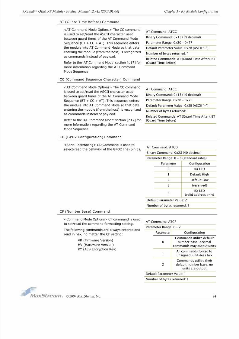
BT (Guard Time Before) Command
<AT Command Mode Options> The CC command
is used to set/read the ASCII character used
between guard times of the AT Command Mode
Sequence (BT + CC + AT). This sequence enters
the module into AT Command Mode so that data
entering the module (from the host) is recognized
as commands instead of payload.
Refer to the ‘AT Command Mode’ section [p17] for
more information regarding the AT Command
Mode Sequence.
CC (Command Sequence Character) Command
<AT Command Mode Options> The CC command
is used to set/read the ASCII character used
between guard times of the AT Command Mode
Sequence (BT + CC + AT). This sequence enters
the module into AT Command Mode so that data
entering the module (from the host) is recognized
as commands instead of payload.
Refer to the ‘AT Command Mode’ section [p17] for
more information regarding the AT Command
Mode Sequence.
CD (GPO2 Configuration) Command
<Serial Interfacing> CD Command is used to
select/read the behavior of the GPO2 line (pin 3).
CF (Number Base) Command
<Command Mode Options> CF command is used
to set/read the command formatting setting.
The following commands are always entered and
read in hex, no matter the CF setting:
VR (Firmware Version)
HV (Hardware Version)
KY (AES Encryption Key)
AT Command: ATCC
Binary Command: 0x13 (19 decimal)
Parameter Range: 0x20 - 0x7F
Default Parameter Value: 0x2B (ASCII “+”)
Number of bytes returned: 1
Related Commands: AT (Guard Time After), BT(Guard Time Before)
AT Command: ATCC
Binary Command: 0x13 (19 decimal)
Parameter Range: 0x20 - 0x7F
Default Parameter Value: 0x2B (ASCII “+”)
Number of bytes returned: 1
Related Commands: AT (Guard Time After), BT
(Guard Time Before)
AT Command: ATCD
Binary Command: 0x28 (40 decimal)
Parameter Range: 0 - 8 (standard rates)
Parameter Configuration
0 RX LED
1 Default High
2 Default Low
3 (reserved)
4RX LED
(valid address only)
Default Parameter Value: 2
Number of bytes returned: 1
AT Command: ATCF
Parameter Range: 0 – 2
Parameter Configuration
0Commands utilize default
number base; decimal
commands may output units
1All commands forced to
unsigned, unit-less hex
2
Commands utilize their
default number base; nounits are output
Default Parameter Value: 1
Number of bytes returned: 1
8/3/2019 Product Manual Xtend Oem Rfmodule
http://slidepdf.com/reader/full/product-manual-xtend-oem-rfmodule 25/71
9XTend™ OEM RF Module ‐ Product Manual v2.x4x [2007.01.04]
© 2007
MaxStream,
Inc.
25
Chapter 3 ‐ RF Module Configuration
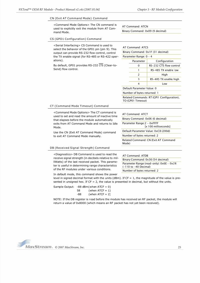
CN (Exit AT Command Mode) Command
<Command Mode Options> The CN command is
used to explicitly exit the module from AT Com-
mand Mode.
CS (GPO1 Configuration) Command
<Serial Interfacing> CS Command is used to
select the behavior of the GP01 pin (pin 9). Thisoutput can provide RS-232 flow control, control
the TX enable signal (for RS-485 or RS-422 oper-
ations).
By default, GP01 provides RS-232 CTS (Clear-to-
Send) flow control.
CT (Command Mode Timeout) Command
<Command Mode Options> The CT command is
used to set and read the amount of inactive time
that elapses before the module automatically
exits from AT Command Mode and returns to Idle
Mode.
Use the CN (Exit AT Command Mode) command
to exit AT Command Mode manually.
DB (Received Signal Strength) Command
<Diagnostics> DB Command is used to read the
receive signal strength (in decibels relative to mil-
liWatts) of the last received packet. This parame-
ter is useful in determining range characteristics
of the RF modules under various conditions.
In default mode, this command shows the power
level in signed decimal format with the units (dBm). If CF = 1, the magnitude of the value is pre-
sented in unsigned hex. If CF = 2, the value is presented in decimal, but without the units.
Sample Output: -88 dBm(when ATCF = 0)
58 (when ATCF = 1)
-88 (when ATCF = 2)
NOTE: If the DB register is read before the module has received an RF packet, the module will
return a value of 0x8000 (which means an RF packet has not yet been received).
AT Command: ATCN
Binary Command: 0x09 (9 decimal)
AT Command: ATCS
Binary Command: 0x1F (31 decimal)
Parameter Range: 0 - 4
Parameter Configuration
0 RS-232 CTS flow control
1 RS-485 TX enable low
2 High
3 RS-485 TX enable high
4 Low
Default Parameter Value: 0
Number of bytes returned: 1
Related Commands: RT (GPI1 Configuration),
TO (GP01 Timeout)
AT Command: ATCT
Binary Command: 0x06 (6 decimal)
Parameter Range:2 - 0xFFFF
[x 100 milliseconds]
Default Parameter Value: 0xC8 (200d)
Number of bytes returned: 2
Related Command: CN (Exit AT Command
Mode)
AT Command: ATDB
Binary Command: 0x36 (54 decimal)
Parameter Range (read-only): 0x6E - 0x28
(-110 to -40 Decimal)
Number of bytes returned: 2
8/3/2019 Product Manual Xtend Oem Rfmodule
http://slidepdf.com/reader/full/product-manual-xtend-oem-rfmodule 26/71
9XTend™ OEM RF Module ‐ Product Manual v2.x4x [2007.01.04]
© 2007
MaxStream,
Inc.
26
Chapter 3 ‐ RF Module Configuration
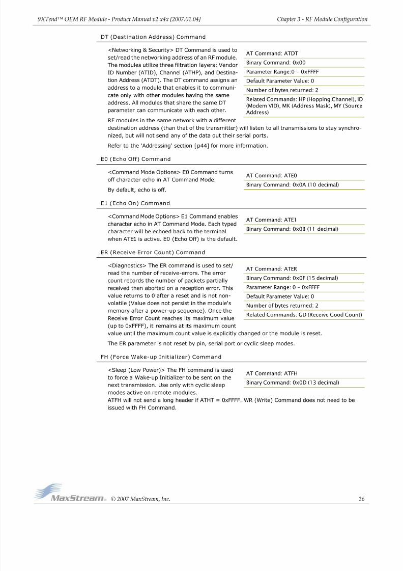
DT (Destination Address) Command
<Networking & Security> DT Command is used to
set/read the networking address of an RF module.
The modules utilize three filtration layers: Vendor
ID Number (ATID), Channel (ATHP), and Destina-
tion Address (ATDT). The DT command assigns an
address to a module that enables it to communi-
cate only with other modules having the same
address. All modules that share the same DT
parameter can communicate with each other.
RF modules in the same network with a different
destination address (than that of the transmitter) will listen to all transmissions to stay synchro-
nized, but will not send any of the data out their serial ports.
Refer to the ‘Addressing’ section [p44] for more information.
E0 (Echo Off) Command
<Command Mode Options> E0 Command turns
off character echo in AT Command Mode.
By default, echo is off.
E1 (Echo On) Command
<Command Mode Options> E1 Command enables
character echo in AT Command Mode. Each typed
character will be echoed back to the terminal
when ATE1 is active. E0 (Echo Off) is the default.
ER (Receive Error Count) Command
<Diagnostics> The ER command is used to set/
read the number of receive-errors. The error
count records the number of packets partially
received then aborted on a reception error. This
value returns to 0 after a reset and is not non-
volatile (Value does not persist in the module's
memory after a power-up sequence). Once the
Receive Error Count reaches its maximum value
(up to 0xFFFF), it remains at its maximum count
value until the maximum count value is explicitly changed or the module is reset.
The ER parameter is not reset by pin, serial port or cyclic sleep modes.
FH (Force Wake-up Initializer) Command
<Sleep (Low Power)> The FH command is used
to force a Wake-up Initializer to be sent on the
next transmission. Use only with cyclic sleep
modes active on remote modules.
ATFH will not send a long header if ATHT = 0xFFFF. WR (Write) Command does not need to beissued with FH Command.
AT Command: ATDT
Binary Command: 0x00
Parameter Range:0 - 0xFFFF
Default Parameter Value: 0
Number of bytes returned: 2
Related Commands: HP (Hopping Channel), ID(Modem VID), MK (Address Mask), MY (Source
Address)
AT Command: ATE0
Binary Command: 0x0A (10 decimal)
AT Command: ATE1
Binary Command: 0x0B (11 decimal)
AT Command: ATER
Binary Command: 0x0F (15 decimal)
Parameter Range: 0 - 0xFFFF
Default Parameter Value: 0
Number of bytes returned: 2
Related Commands: GD (Receive Good Count)
AT Command: ATFH
Binary Command: 0x0D (13 decimal)

8/3/2019 Product Manual Xtend Oem Rfmodule
http://slidepdf.com/reader/full/product-manual-xtend-oem-rfmodule 27/71
9XTend™ OEM RF Module ‐ Product Manual v2.x4x [2007.01.04]
© 2007
MaxStream,
Inc.
27
Chapter 3 ‐ RF Module Configuration
FL (Software Flow Control) Command
<Serial Interfacing> The FL command is used to
configure software flow control. Hardware flow
control is implemented with the module as the
GP01 pin (CTS pin of the OEM RF module), which
regulates when serial data can be transferred to
the module.
FL Command can be used to allow software flowcontrol to also be enabled. The XON character
used is 0x11 (17 decimal). The XOFF character
used is 0x13 (19 decimal)
FS (Forced Synch Time) Command
<RF Interfacing> The FS command only applies
to streaming data. Normally, only the first packet
of a continuous stream contains the full RF initial-
izer. The RF modules then remain synchronized
for subsequent packets of the stream. This
parameter can be used to periodically force an RF
initializer during such streaming. Any break in
UART character reception long enough to drain
the DI Buffer (UART receive buffer) and cause a pause in RF data transmission will also cause an
RF initializer to be inserted on the next transmission.
FT (Flow Control Threshold) Command
<Serial Interfacing> The FT command is used to
set/read the flow control threshold. When FT
bytes have accumulated in the DI buffer (UART
Receive), CTS is de-asserted or the XOFF soft-
ware flow control character is transmitted.
GD (Receive Good Count) Command
<Diagnostics> The GD command is used to set/
read the count of good received RF packets. Its
parameter value is reset to 0 after every reset
and is not non-volatile (The parameter value does
not persist in the RF module's memory after a
power-up sequence). Once the "Receive Good
Count" reaches its maximum value (up to
0xFFFF), it remains at its maximum count value
until the maximum count value is manually
changed or the module is reset.
The GD parameter is not reset by pin, serial port or cyclic sleep modes.
AT Command: ATFL
Binary Command: 0x07 (7 decimal)
Parameter Range: 0 - 1
Parameter Configuration
0Disable software
flow control
1Enable software
flow control
Default Parameter Value: 0
Number of bytes returned: 1
AT Command: ATFS
Binary Command: 0x3E (62 decimal)
Parameter Range:0 - 0xFFFF
[x 10 milliseconds]
Default Parameter Value: 0
Number of bytes returned: 2
AT Command: ATFT
Binary Command: 0x24 (36 decimal)
Parameter Range:
0 - (DI buffer size minus 0x11) [Bytes]
Default Parameter Value: DI Buffer size minus
0x11 (17 decimal)
Number of bytes returned: 2
AT Command: ATGD
Binary Command: 0x10 (16 decimal)
Parameter Range: 0 - 0xFFFF
Default Parameter Value: 0
Number of bytes returned: 2
Related Commands: ER (Receive Error Count)
8/3/2019 Product Manual Xtend Oem Rfmodule
http://slidepdf.com/reader/full/product-manual-xtend-oem-rfmodule 28/71
9XTend™ OEM RF Module ‐ Product Manual v2.x4x [2007.01.04]
© 2007
MaxStream,
Inc.
28
Chapter 3 ‐ RF Module Configuration
HP (Hopping Channel) Command
<Networking & Security> The HP command is
used to set/read the RF module's hopping channel
number. A channel is one of three layers of filtra-
tion available to the module.
In order for modules to communicate with each
other, the modules must have the same channel
number since each channel uses a different hop-ping sequence. Different channels can be used to
prevent modules in one network from listening to
transmissions of another.
HT (Time before Wake-up I nitializer) Command
<Sleep (Low Power)> The HT command is used
to set/read the time of inactivity (no serial or RF
data is sent or received) before a wake-up initial-
izer is sent by a TX (transmitting) RF module. The
HT parameter should be set shorter than inactiv-
ity timeout [ST Command] time of any RX
(receiving) modules operating in Cyclic Sleep
(SM=4-8). The wake-up initializer sent by the TXmodule instructs all RX modules to remain awake
to receive RF data.
From the RX module perspective: After HT time
elapses and the inactivity timeout [ST Command]
is met, the RX module goes into cyclic sleep. In cyclic sleep, the RX module wakes once per sleep
interval [SM Command] to check for a wake-up initializer. When a wake-up initializer is detected,
the module stays awake to receive data. The wake-up initializer must be longer than the cyclic
sleep interval to ensure that sleeping modules detect incoming data.
When HT time elapses, the TX module knows it needs to send a wake-up Initializer for all RX mod-
ules to remain awake and receive the next transmission.
HV (Hardware Version) Command
<Diagnostics> The HV command is used to read
the hardware version of the RF module.
ID (Modem VI D) Command
<Networking & Security> The ID command is
used to set/read the VID (Vendor Identification
Number) of the RF module. RF modules must
have matching VIDs in order to communicate.
AT Command: ATHP
Binary Command: 0x11 (17 decimal)
Parameter Range: 0 - 9
Default Parameter Value: 0
Number of bytes returned: 1
Related Commands: ID (Modem VID), DT(Destination Address), MK (Address Mask)
AT Command: ATHT
Binary Command: 0x03 (3 decimal)
Parameter Range:0 - 0xFFFF
[x 100 milliseconds]
Default Parameter Value: 0xFFFF (wake-up
initializer will not be sent)
Number of bytes returned: 2
Related Commands: LH (Wake-up InitializerTimer), SM (Sleep Mode), ST (Time before
Sleep)
AT Command: ATHV
Parameter Range:0 - 0xFFFF [Read-only]
Minimum Firmware Version Required: v1.x80
AT Command: ATID
Binary Command: 0x27 (39 decimal)
Parameter Range:0x11 - 0x7FFF (user-settable)
0 - 0x10 & 0x8000 - 0xFFFF (factory-set)
Default Parameter Value: 0x3332 (13106d)
Number of bytes returned: 2
8/3/2019 Product Manual Xtend Oem Rfmodule
http://slidepdf.com/reader/full/product-manual-xtend-oem-rfmodule 29/71
9XTend™ OEM RF Module ‐ Product Manual v2.x4x [2007.01.04]
© 2007
MaxStream,
Inc.
29
Chapter 3 ‐ RF Module Configuration
KY (AES Encryption Key) Command
<Networking & Security> The KY command is
used to set the 256-bit AES (Advanced Encryption
Standard) key for encrypting/decrypting data.
Once set, the key cannot be read out of the mod-
ule by any means. The entire payload of the
packet is encrypted using the key and the CRC is
computed across the ciphertext. When encryption
is enabled, each packet carries an additional 16
bytes to convey the random CBC Initialization
Vector (IV) to the receiver(s). The KY value may
be “0” or any 256-bit value (= 64 hex digits = 32 bytes). Any other value, including entering ATKY
by itself with no parameters, causes an error.
A module with the wrong key (or no key) will receive encrypted data, but the data driven out the
serial port will be meaningless. Likewise, a module with a key will receive unencrypted data sent
from a module without a key, but the output will be meaningless. Because CBC mode is utilized,
repetitive data appears differently in different transmissions due to the randomly-generated IV.
LH (Wake-up Initializer Timer) Command
<Sleep (Low Power)> The LH Command is used
to set/read the duration of time during which thewake-up initializer is sent. When receiving mod-
ules are in Cyclic Sleep Mode, they power-down
after a period of inactivity (as specified by the ST
parameter) and will periodically wake and listen
for transmitted data. In order for the receiving
modules to remain awake, they must detect
~35ms of the wake-up initializer.
LH Command must be used whenever a receiving
module is operating in Cyclic Sleep Mode. The
Wake-up Initializer Time must be longer than the cyclic sleep time that [as determined by SM
(Sleep Mode) parameter]. If the wake-up initializer time were less than the Cyclic Sleep interval,
the connection would be at risk of missing the wake-up initializer transmission.
Refer to figures loated under the SM command description to view diagrams of correct and incor-
rect configurations. The images emphasize that the LH value must be greater than the SM value.
MD (RF Mode) Command
<Networking & Security> The MD command is
used to select/read the settings that enable the
Polling and Repeater Modes on the module.
Polling Mode - A ‘Polling Base’ is responsible for
polling remotes. A ‘Polling Remote’ requires a poll
in order to transmit.
Repeater Mode - A ‘Repeater’ re-sends RF data
unless the transmission is addressed to it or if the
transmission has already been detected. A
‘Repeater End Node’ handles repeated messages,
but will not repeat the message over-the-air.
Refer to the Polling and Repeater Mode sections of
the ‘RF Communication Modes’ chapter for more
information.
AT Command: ATKY
Binary Command: 0x3C (60 decimal)
Parameter Range:0 - (any other 64-digit hex valid key)
Default Parameter Value: 0 (disabled)
Number of bytes returned: 2Number Base: Always Hexadecimal
AT Command: ATLH
Binary Command: 0x0C (12 decimal)
Parameter Range:0 - 0xFF[x 100 milliseconds]
Default Parameter Value: 1
Number of bytes returned: 1
Related Commands: HT (Time before Wake-up
Initializer), SM (Sleep Mode), ST (Time beforeSleep)
AT Command: ATMD
Binary Command: 0x31 (49 decimal)
Parameter Range: 0 - 6
Parameter Configuration
0Transparent Operation
(Repeater Base)
1 [reserved - not used]
2 [reserved - not used]
3 Polling Base
4 Polling Remote
5 Repeater
6 Repeater End Node
Default Parameter Value: 0
Number of bytes returned: 1
Minimum Firmware Version Required: 2.x20

8/3/2019 Product Manual Xtend Oem Rfmodule
http://slidepdf.com/reader/full/product-manual-xtend-oem-rfmodule 30/71
9XTend™ OEM RF Module ‐ Product Manual v2.x4x [2007.01.04]
© 2007
MaxStream,
Inc.
30
Chapter 3 ‐ RF Module Configuration
MK (Address Mask) Command
<Networking & Security> The MK command is
used to set/read the Address Mask of a module.
All RF data packets contain the Destination
Address of the TX (transmitting) module. When a
packet is received, the TX module Destination
Address is logically "ANDed" (bitwise) with the
Address Mask of the RX (receiving) module. Theresulting value must match the Destination
Address or Address Mask of the RX module for the
packet to be received and sent out the RX mod-
ule's DO (Data Out) pin. If the "ANDed" value does not match the Destination Address or Address
Mask of the RX module, the packet is discarded.
Sniffer Mode (when MK = 0): ACK requests are ignored and every RX (receive) frame is sent to
the UART, without regard for repeated frames.
All “0” values are treated as irrelevant values and ignored.
Refer to the ‘Addressing’ section [p44] for more information.
MT (Multi-transmit) Command
<Networking & Security> The MT command isused to enabled multiple transmissions of RF data
packets. When Multi-transmit Mode is enabled
(MT > 0), packets do not request an ACK
(acknowledgement) from the receiving RF mod-
ule(s). MT takes precedence over RR, so if both
MT and RR are non-zero, then MT+1 packets will
be sent (with no ACK requests).
When a receiving module receives a packet with
remaining forced retransmissions, it calculates
the length of the packet and inhibits transmission
for the amount of time required for all retransmissions. Thereafter, a random number of delay
slots are inserted between 0 and RN before transmission is allowed from the receiving module(s).
This prevents all listening modules from transmitting at once upon conclusion of a multiple trans-mission event (when RN > 0).
NOTE: The actual number of forced transmissions is the parameter value plus one. For example, if
MT = 1, two transmissions of each packet will be sent.
Refer to the ‘Multi-transmit Mode’ section [p46] for more information.
MY (Source Address) Command
<Networking & Security> The MY command is
used to set/read the Source Address of the RF
module.
Refer to the ‘Addressing’ section [p44] for more
information.
AT Command: ATMK
Binary Command: 0x12 (18 decimal)
Parameter Range:0 - 0xFFFF
Default Parameter Value: 0xFFFF (65535d)
Number of bytes returned: 2
Related Commands: DT (Destination Address),HP (Hopping Channel), ID (Modem VID), MY(Source Address)
AT Command: ATMT
Binary Command: 0x3D (61 decimal)
Parameter Range: 0 - 0xFF
Default Parameter Value:0 (no forced
retransmissions)
Number of bytes returned: 1
Related Commands: Networking (DT, MK, MY,
RN, TT), Serial Interfacing (BR, PK, RB, RO), RF
Interfacing (FS)
AT Command: ATMY
Binary Command: 0x2A (42 decimal)
Parameter Range: 0 - 0xFFFF
Default Parameter Value: 0xFFFF (Disabled -
DT (Destination Address) parameter serves asboth source and destination address.)
Number of bytes returned: 2
Related Commands: DT (Destination Address),
HP (Hopping Channel), ID (Modem VID), MK
(Address Mask)
8/3/2019 Product Manual Xtend Oem Rfmodule
http://slidepdf.com/reader/full/product-manual-xtend-oem-rfmodule 31/71
9XTend™ OEM RF Module ‐ Product Manual v2.x4x [2007.01.04]
© 2007
MaxStream,
Inc.
31
Chapter 3 ‐ RF Module Configuration
NB (Parity) Command
<Serial Interfacing> The NB command is used to
select/read the parity settings of the RF module
for UART communications.
PB (Polling Begin Address) Command
<Networking & Security> PB command is used to
set/read the module’s Polling Begin Address - the
first address polled Polling Mode is enabled.
Polling Operations: The ‘Polling Base’ (MD = 3)
cycles through a sequential range of addresses,
polling each ‘Polling Remote’ (MD = 4). The base
then waits for a response & proceeds to the next
‘Polling Remote’. Each ‘Polling Remote’ responds
by sending the data from the Data In buffer fol-
lowing the RB & RO parameters. When there is no
eligible data to send, the ‘Polling Remote’ will not respond. The ‘Polling Base’ will move to the next
address in the polling sequence after a short delay.
PD (Minimum P olling Delay) Command
<Networking & Security> The PD command is
used to set/read Polling Delay (Base, MD=3) or
Polling Timeout (Remote, MD=4).
Polling Delay (Base) is the time between pollingcycles. The Polling Base will start the polling cycle
after sending the first poll. After the polling cycle
has completed, the timer is restarted.
Polling Timeout (Remote) is the amount of time
the remote unit will hold data from the serial port
before discarding it. Data entered within the PD
time of the poll is transmitted and not discarded.
PE (Po lling End Address) Command
<Networking & Security> PE command is used to
set/read the module’s Polling End Address - the
last address polled when Polling Mode is enabled.
Polling Operations: The ‘Polling Base’ (MD = 3)
cycles through a sequential range of addresses,
polling each ‘Polling Remote’ (MD = 4). The base
then waits for a response & proceeds to the next
‘Polling Remote’. Each ‘Polling Remote’ responds
by sending data from the DI buffer following the
RB & RO parameters. When there is no eligible
data to send, the ‘Polling Remote’ will not respond. The ‘Polling Base’ will move to the next address
in the polling sequence after a short delay.
AT Command: ATNB
Binary Command: 0x23 (35 decimal)
Parameter Range: 0 - 4
Parameter Configuration
08-bit (no parity or7-bit (any parity)
1 8-bit even2 8-bit odd
3 8-bit mark
4 8-bit space
Default Parameter Value: 0
Number of bytes returned: 1
AT Command: ATPB
Binary Command: 0x45 (69 decimal)
Parameter Range: 0 - 0xFFFF
Default Parameter Value: 0
Number of bytes returned: 2
Minimum Firmware Version Required: 2.x20
Related Commands: MD (RF Mode), PE (Polling
End Address), PD (Minimum Polling Delay)
AT Command: ATPD
Binary Command: 0x47 (71 decimal)
Parameter Range: 0 - 0xFFFF
(Base: [x 1ms], Remote: [x 10ms])
Default Parameter Value: 0
Number of bytes returned: 2
Minimum Firmware Version Required: 2.x20
Related Commands: MD (RF Mode), PB (PollingBegin Address), PE (Polling End Address)
AT Command: ATPE
Binary Command: 0x46 (70 decimal)
Parameter Range: 0 - 0xFFFF
Default Parameter Value: 0
Number of bytes returned: 2
Minimum Firmware Version Required: 2.x20
Related Commands: MD (RF Mode), PB (Polling
Begin Address), PD (Minimum Polling Delay)
8/3/2019 Product Manual Xtend Oem Rfmodule
http://slidepdf.com/reader/full/product-manual-xtend-oem-rfmodule 32/71
9XTend™ OEM RF Module ‐ Product Manual v2.x4x [2007.01.04]
© 2007
MaxStream,
Inc.
32
Chapter 3 ‐ RF Module Configuration
PK (Maximum RF Packet Size) Command
<RF Interfacing> The PK command is used to set/
read the maximum size of RF packets transmitted
from an RF module. The maximum packet size
can be used along with the RB and RO parameters
to implicitly set the channel dwell time.
If PK is set above 256 and BR is subsequently
changed to 0, PK will automatically be lowered to256 and a warning will be raised (refer to the BR
(RF Data Rate) and WN (Warning Data) com-
mands for details).
Changes to the PK parameter may have a second-
ary effect on the RB (Packetization Threshold) parameter. RB must always be less than or equal to
PK. If PK is changed to a value that is less than the current value of RB, the RB value is automati-
cally lowered to be equal to PK.
* When BR = 0 (9600 baud), the maximum PK value is 0x100 (256d). When BR = 1 (115,200
baud), the maximum PK value is 0x800 (2048d).
PL (TX Pow er Level) Command
<RF Interfacing> The PL command is used to set/read the power level at which the RF module
transmits data.
PW (Pin W ake-up) Command
<Sleep (Low Power)> Under normal operation, an
RF module in Cyclic Sleep Mode cycles from an
active state to a low-power state at regular inter-
vals until data is ready to be received. If the PW
parameter is set to 1, the SLEEP pin (pin 8) can
be used to awaken the module from Cyclic Sleep.
When the SLEEP Pin is de-asserted (low), the
module will be fully operational and will not go
into Cyclic Sleep.
Once the SLEEP pin is asserted, the module will
remain active for the period of time specified bythe ST (Time before Sleep) parameter and will
return to Cyclic Sleep Mode (if no data is ready to
be transmitted). PW Command is only valid if Cyclic Sleep has been enabled.
AT Command: ATPK
Binary Command: 0x29 (41 decimal)
Parameter Range:1 - 0x800 [Bytes]
Default Parameter Value:0x100* or 0x800*(256 or 2048 decimal)
Number of bytes returned: 2Related Commands: BR (RF Data Rate) RB(Packetization Threshold), RO (Packetization
Timeout), WN (Warning Data)
AT Command: ATPL
Binary Command: 0x3A (58 decimal)
Parameter Range: 0 - 4
Parameter Configuration
0 1 mW
1 10 mW
2 100 mW
3 500 mW
4 1000 mW (1 Watt)
Default Parameter Value: 4
Number of bytes returned: 1
AT Command: ATPW
Binary Command: 0x1D (29 decimal)
Parameter Range: 0 - 1
Parameter Configuration
0 Disabled
1 Enabled
Default Parameter Value: 0
Number of bytes returned: 1
Related Commands: SM (Sleep Mode), ST(Time before Sleep)
8/3/2019 Product Manual Xtend Oem Rfmodule
http://slidepdf.com/reader/full/product-manual-xtend-oem-rfmodule 33/71
9XTend™ OEM RF Module ‐ Product Manual v2.x4x [2007.01.04]
© 2007
MaxStream,
Inc.
33
Chapter 3 ‐ RF Module Configuration
RB (Packetization Threshold) Command
<Serial Interfacing> The RB command is used to
set/read the character threshold value.
RF transmission begins after data is received in
the DI Buffer and either of the following criteria is
met:
• RB characters received by the UART
• RO character times of silence detected on theUART receive lines (after receiving at least 1Byte of data)
If PK (Max. RF Packet Size) is lowered below the
value of RB, RB is automatically lowered to match the PK value. If (RO = 0), RB bytes must be
received before beginning transmission.
Note: RB and RO criteria only apply to the first packet of a multi-packet transmission. If data
remains in the DI Buffer after the first packet, transmissions will continue in a streaming manner
until there is no data left in the DI Buffer (UART receive buffer).
RC (Ambient Pow er - Single Channel) Command
<Diagnostics> The RC command is used to exam-
ine and report the power level on a given channel.Sample output: -78 dBm [when CF = 0]
4e [when CF = 1]
-78 [when CF = 2]
RE (Restore Defaults) Command
<Diagnostics> The RE command is used to
restore all configurable parameters to their fac-
tory default settings.
The RE Command does not cause default values
to be stored to non-volatile (persistent) memory. For the restored default settings to persist in the
module’s non-volatile memory and be saved in the event of RF module reset or power-down, the
WR (Write) command must be issued prior to power-down or reset.
RM (Ambient P ower - All Channels) Command
<Diagnostics> The RM command is used to
examine and report power levels on all channels.
If no parameter is given, the channels are
scanned one time. If a parameter is given, the
channels are repeatedly scanned for that number
of seconds. The maximum power level seen for
each channel is reported (i.e. peak hold).
A graphical spectrum analyzer can be implemented by repeatedly sending the RM command (with
no arguments) and reading the resultant 50 power levels (this is easiest to do when CF = 1 or 2).
Sample output [when CF = 0]: Ch 0: -100 dBm
Ch 1: -103 dBm
...
Ch 49: -99 dBm
Sample output [when CF = 1]: 64
67
...
63
Sample output [when CF = 2]: 100
-103
…
-99
AT Command: ATRB
Binary Command: 0x20 (32 decimal)
Parameter Range:0 - PK parameter value(up to 0x800 Bytes)
Default Parameter Value: 0x800 Bytes
Number of bytes returned: 2Related Commands: BR (RF Data Rate), PK (RFPacket Size), RO (Packetization Timeout)
AT Command: ATRC
Parameter Range (read-only): 0 - 0x31 [dBm]
Number of bytes returned: 1
Related Commands: RM (Ambient Power - All
Channels)
AT Command: ATRE
Binary Command: 0x0E (14 decimal)
AT Command: ATRM
Parameter Range: no parameter - 0x7D0)
Number of bytes returned: 2
Related Commands: RC (Ambient Power -Single channel)

8/3/2019 Product Manual Xtend Oem Rfmodule
http://slidepdf.com/reader/full/product-manual-xtend-oem-rfmodule 34/71
9XTend™ OEM RF Module ‐ Product Manual v2.x4x [2007.01.04]
© 2007
MaxStream,
Inc.
34
Chapter 3 ‐ RF Module Configuration
RN (Delay Slots) Command
<Networking & Security> The RN command is
used to set/read the time delay that the transmit-
ting RF module inserts before attempting to
resend a packet. If the transmitting module fails
to receive an acknowledgement after sending a
packet, it inserts a random number of delay slots
(ranging from 0 to (RN minus 1)) before attempt-
ing to resend the packet. Each delay slot is 5
msec (when BR=1) and 54 msec (when BR=0).
If two modules attempt to transmit at the same
time, the random time delay after packet failure allows only one module to transmit the packet
successfully; while the other module waits until the channel available for RF transmission.
RN Command is only applicable if retries have been enabled [RR (Retries) Command] or if forced
delays will be inserted into a transmission [TT (Streaming Limit) Command].
RO (Packetization Timeout) Command
<Serial Interfacing> The RO command is used to
set/read the Packetization Timeout setting. RF
transmission begins when data is in the DI buffer
and either of the following criteria are met:
• RO character times of silence on the UARTreceive lines (after receiving at least 1 byte)
• RB characters have been received by theUART
RB and RO criteria only apply to the first packet of
a multi-packet transmission. If data remains in
the DI Buffer (UART receive) after the first packet, transmissions will continue in a streaming man-
ner until there is no data left in the DI Buffer.
When RO is the transmission-beginning criteria: The actual time between the reception of
the last character from the UART and the beginning of RF transmission will be at least 800 µsec
longer than the actual RO time to allow for transmission setup. Additionally, it is subject to 100-
200 µsec of additional uncertainty, which could be significant for small values of RO at high UARTbit rates.
The correct UART character time (10, 11, or 12 bits) is calculated based on the following criteria:
• 1 start bit
• 8 data bits
• 0 or 1 parity bit [as determined by the NB (Parity) Command)
• 1 or 2 stop bits [as determined by SB (Stop Bits) Command]
AT Command: ATRN
Binary Command: 0x19 (25 decimal)
Parameter Range:0 - 0xFF [38 ms slots]
Default Parameter Value: 0(no delay slots inserted)
Number of bytes returned: 1Related Commands: RR (Retries), TT(Streaming Limit)
AT Command: ATRO
Binary Command: 0x21 (33 decimal)
Parameter Range:0 - 0xFFFF[ x UART character times ]
Default Parameter Value: 3
Number of bytes returned: 2
Related Commands: RB (PacketizationThreshold)
8/3/2019 Product Manual Xtend Oem Rfmodule
http://slidepdf.com/reader/full/product-manual-xtend-oem-rfmodule 35/71
9XTend™ OEM RF Module ‐ Product Manual v2.x4x [2007.01.04]
© 2007
MaxStream,
Inc.
35
Chapter 3 ‐ RF Module Configuration
RP (RSSI PWM Timer) Command
<Diagnostics> RP Command is used to enable a
PWM ("Pulse Width Modulation") output on the
Config/RSSI pin (pin 11 of the OEM RF Module).
The pin is calibrated to show the difference
between received signal strength and the sensi-
tivity level of the RF module. PWM pulses vary
from zero to 95 percent. Zero percent means the
received RF signal is at or below the published
sensitivity level of the module.
The following table shows dB levels above sensitivity and PWM values (The total time period of the
PWM output is 8.32 ms. PWM output consists of 40 steps and therefore the minimum step size is
0.208 ms.):
A non-zero value defines the time that PWM output is active with the RSSI value of the last
received RF packet. After the set time when no RF packets are received, PWM output is set low (0
percent PWM) until another RF packet is received. PWM output is also set low at power-up. A
parameter value of 0xFF permanently enables PWM output and always reflects the value of the last
received RF packet.
The Config/RSSI pin is shared between PWM output and Config input. When the module is pow-
ered, the Config pin is an input. During the power-up sequence, if RP parameter is a non-zero
value, the Config pin is configured as an output and set low until the first RF packet is received.
With a non-zero RP parameter, the Config pin is an input for RP ms after power up.
RR (Retries) Command
<Networking & Security> The RR command is
used to set/read the maximum number of retries
sent for a given RF packet. When RR Command is
enabled (RR>0), RF packet retries and ACKs
(acknowledgements) are enabled.
Exceptions: If the MT command in enabled
(MT>0) or if a broadcast Destination Address is
used (DT = 0xFFFF); RF packet retries and ACKs are disabled.
After transmitting a packet, the transmitting RF module waits to receive an acknowledgement
from a receiving module. If the acknowledgement is not received in the period of time specified by
RN (Delay Slots) Command, the original packet is transmitted again. The RF packet is transmitted
repeatedly until an acknowledgement is received or until the packet is sent RR times.
Table 3‐02. PWM Values
dBm above sensitivityPWM percentage
(high period / total period)
10 20%
20 35%
30 50%
AT Command: ATRP
Binary Command: 0x22 (34 decimal)
Parameter Range:0 - 0xFF[x 100 milliseconds]
Default Parameter Value: 0x20 (32d)
Number of bytes returned: 1
AT Command: ATRR
Binary Command: 0x18 (24 decimal)Parameter Range:0 - 0xFF
Default Parameter Value: 0x0A (10 decimal)
Number of bytes returned: 1

8/3/2019 Product Manual Xtend Oem Rfmodule
http://slidepdf.com/reader/full/product-manual-xtend-oem-rfmodule 36/71
9XTend™ OEM RF Module ‐ Product Manual v2.x4x [2007.01.04]
© 2007
MaxStream,
Inc.
36
Chapter 3 ‐ RF Module Configuration
RT (GPI1 Configuration) Command
<Serial Interfacing> The RT command is used to
set/read the behavior of the GPI1 pin (pin 10) of
the OEM RF Module. The pin can be configured to
enable binary programming or RTS flow control.
SB (Stop Bits) Command
<Serial Interfacing> The SB Command is used to
set/read the number of stop bits in the data
packet.
SH (Serial Number High) Command
<Diagnostics> SH Command is used to set/read
the serial number high word of the RF module.
SL (Serial Number Low) Command
<Diagnostics> SL Command is used to set/read
the serial number low word of the RF module.
AT Command: ATRT
Binary Command: 0x16 (22 decimal)
Parameter Range: 0 - 2
Parameter Configuration
0 Disabled
1 Enable BinaryProgramming
2 Enable RTS Flow Control
Default Parameter Value: 0
Number of bytes returned: 1
AT Command: ATSB
Binary Command: 0x37 (55 decimal)
Parameter Range: 0 - 1
Parameter Configuration
0 1 stop bit
1 2 stop bits
Default Parameter Value: 0
Number of bytes returned: 1
AT Command: ATSH
Binary Command: 0x25 (37 decimal)
Parameter Range (read-only): 0 - 0xFFFF
Default Parameter Value: varies
Number of bytes returned: 2
Related Commands: SL (Serial Number Low)
AT Command: ATSL
Binary Command: 0x26 (38 decimal)
Parameter Range (read-only): 0 - 0xFFFF
Default Parameter Value: varies
Number of bytes returned: 2
Related Commands: SH (Serial Number High)
8/3/2019 Product Manual Xtend Oem Rfmodule
http://slidepdf.com/reader/full/product-manual-xtend-oem-rfmodule 37/71
9XTend™ OEM RF Module ‐ Product Manual v2.x4x [2007.01.04]
© 2007
MaxStream,
Inc.
37
Chapter 3 ‐ RF Module Configuration
SM (Sleep Mode) Command
<Sleep Mode (Low Power)> The SM Command is
used to set/read the RF module's Sleep Mode set-
tings that configure the module to run in states
that require minimal power consumption.
For more information regarding Sleep Modes,
refer to the Sleep Mode sections [p15]
ST (Time before Sleep) Command
<Sleep Mode (Low Power)> The ST Command is
used to set/read the period of time (in millisec-
onds) in which the RF module remains inactive
before entering Sleep Mode.
For example, if the ST Parameter is set to 0x64
(100 decimal), the module will enter into Sleep
mode after 10 seconds of inactivity (no transmit-
ting or receiving).
This command can only be used if Cyclic Sleep or
Serial Port Sleep Mode settings have been
selected using SM (Sleep Mode) Command.
TP (Board Temperature) Command
<Diagnostics> TP Command is used to read the
current temperature of the board.
Sample Output: 26 C [when ATCF = 0]
1A [when ATCF = 1]
26 [when ATCF = 2].
AT Command: ATSM
Binary Command: 0x01
Parameter Range: 0 - 8 (3 is reserved)
Parameter Configuration
0 Disabled
1 Pin Sleep
2 Serial Port Sleep
3 [reserved]
4Cyclic 1.0 second sleep(RF module wakes every
1.0 seconds)
5 Cyclic 2.0 second sleep
6 Cyclic 4.0 second sleep
7 Cyclic 8.0 second sleep
8 Cyclic 16.0 second sleep
Default Parameter Value: 0
Number of bytes returned: 1
Related Commands:
Pin Sleep - PC (Power-up Mode), PW (PinWake-up)
Serial Port Sleep - ST (Time before Sleep)
Cyclic Sleep - ST (Time before Sleep), LH
(Wake-up Initializer Timer), HT (Time Before
Wake-up Initializer), PW (Pin Wake-up)
AT Command: ATST
Binary Command: 0x02 (2 decimal)
Parameter Range:(ATAT+3) - 0x7FFF
[x 100 milliseconds]Default Parameter Value: 0x64 (100 decimal)
Number of bytes returned: 2
Related Commands: SM (Sleep Mode), LH(Wake-up Initializer Timer), HT (Time before
Wake-up Initializer)
AT Command: ATTP
Binary Command: 0x38 (56 decimal)
Parameter Range (read-only): 0- 0x7FNumber of bytes returned: 1
Related Command: WN (Warning Data)

8/3/2019 Product Manual Xtend Oem Rfmodule
http://slidepdf.com/reader/full/product-manual-xtend-oem-rfmodule 38/71
9XTend™ OEM RF Module ‐ Product Manual v2.x4x [2007.01.04]
© 2007
MaxStream,
Inc.
38
Chapter 3 ‐ RF Module Configuration
TR (Transmit Error Count) Command
<Diagnostics> The TR command is used to report
the number of retransmit failures. This number is
incremented each time a packet is not acknowl-
edged within the number of retransmits specified
by the RR (Retries) parameter. The number of
packets therefore are counted that were not suc-
cessfully received and subsequently discarded.
The TR parameter is not non-volatile and is reset
to zero when the RF module is reset.
TT (Streaming Limit) Command
<Networking & Security> The TT command is
used to set/read the limit on the number of bytes
that can be sent out before a random delay is
issued.
If an RF module is sending a continuous stream of
RF data, a delay is inserted which stops its trans-
mission and allows other modules time to trans-
mit (once it sends TT bytes of data). Inserted
random delay lasts between 1 & 'RN + 1' delay slots, where each delay slot lasts 38 ms.
The TT command can be used to simulate full-duplex behavior.
TX (Transmit Only) Command
<RF Interfacing> The TX command is used to set/
read the transmit/receive behaviors of the RF
module. Setting a module to TX-only (TX = 1)
may reduce latency because the transmitting
module will never be confined to receiving data
from other modules.
VL (Firmw are Version - Verbose)
<Diagnostics> The VL command is used to read
the verbose firmware version of the RF module.
VR (Firmw are Version - Short) Command
<Diagnostics> The VR command is used to readthe firmware version of the RF module.
Note: Firmware versions contain four significant
digits - “A.B.C.D”. If B=2, the module is pro-
grammed for operation in Australia only.
AT Command: ATTR
Binary Command: 0x1B (27 decimal)
Parameter Range: 0 - 0xFFFF
Default Parameter Value: 0
Number of bytes returned: 2
Related Commands: RR (Retries)
AT Command: ATTT
Binary Command: 0x1A (26 decimal)
Parameter Range:0 - 0xFFFF
Default Parameter Value: 0 (disabled)
Number of bytes returned: 2
Related Commands: RN (Delay Slots)
AT Command: ATTX
Binary Command: 0x3F (63 decimal)
Parameter Range: 0 - 1
Parameter Configuration
0 TX & RX
1 TX-only
Default Parameter Value: 0Number of bytes returned: 1
AT Command: ATVL
Parameter Range: returns string
Default Parameter Value: 0
Number of bytes returned: 2
AT Command: ATVR
Binary Command: 0x14 (20 decimal)
Parameter Range (read-only): 0 - 0xFFFF
Number of bytes returned: 2
8/3/2019 Product Manual Xtend Oem Rfmodule
http://slidepdf.com/reader/full/product-manual-xtend-oem-rfmodule 39/71
9XTend™ OEM RF Module ‐ Product Manual v2.x4x [2007.01.04]
© 2007
MaxStream,
Inc.
39
Chapter 3 ‐ RF Module Configuration
WA (Active Warning Numbers) Command
<Diagnostics> The WA command reports the
warning numbers of all active warnings - one
warning number per line. No further information
is shown and warning counts are not reset.
Sample Output (indicates warnings 1 and 3 are currently active): 1
3
OK
WN (W arning Data) Command
<Diagnostics> WN command is used to report the
following data for all active and sticky warnings:
• Warning number & description
• Number of occurrences since the last WN or WS command
• Whether the warning is currently active
Warnings, which are not currently active and have not been active since the last issuance of the
WN or WS commands, are not displayed. The WN command also resets all non-zero warning
counts; except for warnings that are presently active, which are set to 1.
Sample output: Warning 4: Over-temperature
5 occurrences; presently inactive.
WR (Write) Command
<(Special)> The WR command is used to write
configurable parameters to non-volatile memory
(Values remain in the module's memory until
overwritten by another use of WR Command).
If changes are made without writing them to non-volatile memory, the module will revert back to
previously saved parameters the next time the module is powered-on.
If the non-volatile user configuration is not correct, WR will re-attempt (up to 3x). If all three
attempts fail, the command will return an ERROR alert.
WS (Sticky Warning Numbers) Command
<Diagnostics> The WS command reports warning
numbers of all warnings active since the last use
of the WS or WN command (including any warn-
ings which are currently active). This command
also resets all non-zero warning counts, except
for warnings that are presently active, which are set to 1.
Warning # Description
1Under-voltage. This is caused if the supply voltage falls below the minimum threshold for the lowest power level (2.8 V). If/when the voltagerises above the threshold, the warning is deactivated. The module will not transmit below this voltage threshold.
2 Over-voltage. This is caused if the supply voltage exceeds 5.75 V. Transmission is not allowed while this warning is active.
3Under-temperature. This is caused if the temperature sensed by the module is less than -40 C. The module does not artificially limit operationwhile this warning is active, but module functionality is not guaranteed.
4Over-temperature. This is caused if the temperature sensed by the module is greater than 105 C. The module does not allow transmission nor reception while this warning is active. The warning is deactivated when the temperature falls to 100 C.
5Power reduced. This is caused if the transmit power has to be reduced from the level programmed by PL Command due to insufficient supplyvoltage. The 1 W power level requires 4.75 V or higher; 500 mW requires 3.0 V or higher; 100 mW, 10 mW and 1 mW require 2.8 V or higher.
6Default calibration data in flash. This is caused if the module-specific power calibration data is either not present or is invalid, or if none of theparameters have been modified from their default values. Power levels may be incorrect.
7
Default configuration parameters in flash. This is caused if user-modifiable parameters (i.e. those stored by a 'WR' command) in flash are all thecompiled-in default values. This is caused if the user configuration is found to be not present or invalid at power-up and there is no custom
configuration, or if no user-modifiable parameters have been modified from the compiled-in defaults. Modification of one or more parameterswithout the subsequent WR to commit the changes to flash will not deactivate this warning, since it reflects the status of the parameters in flash.Note that this warning does not reflect usage of the custom configuration defaults, only usage of the compiled-in defaults.
8Default factory configuration parameters in flash. This is caused if the factory parameters in flash are all the default values. This is caused if thefactory configuration is found to be not present or invalid at power-up, or if no factory parameters have been modified.
AT Command: ATWA
Parameter Range:Returns string - one
warning number per line.
AT Command: ATWN
Parameter Range: returns string
AT Command: ATWR
Binary Command: 0x08
AT Command: ATWS
Parameter Range (read-only): 1 - 8
Number of bytes returned: 1
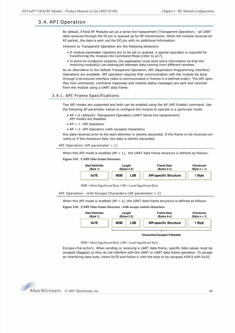
8/3/2019 Product Manual Xtend Oem Rfmodule
http://slidepdf.com/reader/full/product-manual-xtend-oem-rfmodule 40/71
9XTend™ OEM RF Module ‐ Product Manual v2.x4x [2007.01.04]
© 2007
MaxStream,
Inc.
40
Chapter 3 ‐ RF Module Configuration
3.4. AP I Operation
By default, XTend RF Modules act as a serial line replacement (Transparent Operation) - all UART
data received through the DI pin is queued up for RF transmission. When the module receives an
RF packet, the data is sent out the DO pin with no additional information.
Inherent to Transparent Operation are the following behaviors:
• If module parameter registers are to be set or queried, a special operation is required fortransitioning the module into Command Mode [refer to p17].
• In point-to-multipoint systems, the application must send extra information so that thereceiving module(s) can distinguish between data coming from different remotes.
As an alternative to the default Transparent Operation, API (Application Programming Interface)
Operations are available. API operation requires that communication with the module be done
through a structured interface (data is communicated in frames in a defined order). The API spec-
ifies how commands, command responses and module status messages are sent and received
from the module using a UART data frame.
3.4.1. API Frame Specifications
Two API modes are supported and both can be enabled using the AP (API Enable) command. Use
the following AP parameter values to configure the module to operate in a particular mode:
• AP = 0 (default): Transparent Operation (UART Serial line replacement)
API modes are disabled.
• AP = 1: API Operation
• AP = 2: API Operation (with escaped characters)
Any data received prior to the start delimiter is silently discarded. If the frame is not received cor-
rectly or if the checksum fails, the data is silently discarded.
API Operation (AP parameter = 1)
When this API mode is enabled (AP = 1), the UART data frame structure is defined as follows:
Figure 3‐01. UART Data Frame Structure:
MSB = Most Significant Byte, LSB = Least Significant Byte
API Operation - with Escape Characters (AP parameter = 2)
When this API mode is enabled (AP = 2), the UART data frame structure is defined as follows:
Figure 3‐02. UART Data Frame Structure ‐ with escape control characters:
MSB = Most Significant Byte, LSB = Least Significant Byte
Escape characters. When sending or receiving a UART data frame, specific data values must be
escaped (flagged) so they do not interfere with the UART or UART data frame operation. To escape
an interfering data byte, insert 0x7D and follow it with the byte to be escaped XOR’d with 0x20.
Start Delimiter
(Byte 1)
Length
(Bytes 2-3)
Frame Data
(Bytes 4-n)
Checksum
(Byte n + 1)
0x7E MSB LSB API-specific Structure 1 Byte
Start Delimiter
(Byte 1)
Length
(Bytes 2-3)
Frame Data
(Bytes 4-n)
Checksum
(Byte n + 1)
0x7E MSB LSB API-specific Structure 1 Byte
Characters Escaped If Needed
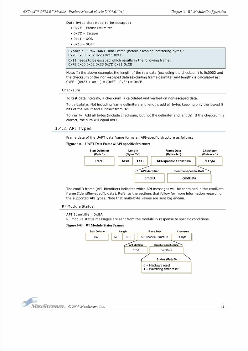
8/3/2019 Product Manual Xtend Oem Rfmodule
http://slidepdf.com/reader/full/product-manual-xtend-oem-rfmodule 41/71
9XTend™ OEM RF Module ‐ Product Manual v2.x4x [2007.01.04]
© 2007
MaxStream,
Inc.
41
Chapter 3 ‐ RF Module Configuration
Data bytes that need to be escaped:
• 0x7E – Frame Delimiter
• 0x7D – Escape
• 0x11 – XON
• 0x13 – XOFF
Note: In the above example, the length of the raw data (excluding the checksum) is 0x0002 and
the checksum of the non-escaped data (excluding frame delimiter and length) is calculated as:
0xFF - (0x23 + 0x11) = (0xFF - 0x34) = 0xCB.
Checksum
To test data integrity, a checksum is calculated and verified on non-escaped data.
To calculate: Not including frame delimiters and length, add all bytes keeping only the lowest 8
bits of the result and subtract from 0xFF.
To verify: Add all bytes (include checksum, but not the delimiter and length). If the checksum is
correct, the sum will equal 0xFF.
3.4.2. AP I Types
Frame data of the UART data frame forms an API-specific structure as follows:
Figure 3‐03. UART Data Frame & API‐specific Structure:
The cmdID frame (API-identifier) indicates which API messages will be contained in the cmdData
frame (Identifier-specific data). Refer to the sections that follow for more information regarding
the supported API types. Note that multi-byte values are sent big endian.
RF Module Status
API Identifier: 0x8A
RF module status messages are sent from the module in response to specific conditions.
Figure 3‐04. RF Module Status Frames
Example - Raw UART Data Frame (before escaping interfering bytes):
0x7E 0x00 0x02 0x23 0x11 0xCB
0x11 needs to be escaped which results in the following frame:0x7E 0x00 0x02 0x23 0x7D 0x31 0xCB
Length
(Bytes 2-3)
Checksum
(Byte n + 1)
MSB LSB 1 Byte
Start Delimiter
(Byte 1)
0x7E
Frame Data
(Bytes 4-n )
API-specific Structure
Identifier-specific Data
cmdData
API Identifier
cmdID
cmdData0x8A
Length ChecksumStart Delimiter Frame Data
Identifier-specific DataAPI Identifier
MSB LSB0x7E 1 ByteAPI-specific Structure
Status (Byte 5)
0 = Hardware reset1 = Watchdog timer reset
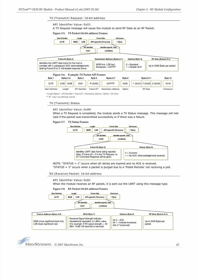
8/3/2019 Product Manual Xtend Oem Rfmodule
http://slidepdf.com/reader/full/product-manual-xtend-oem-rfmodule 42/71
9XTend™ OEM RF Module ‐ Product Manual v2.x4x [2007.01.04]
© 2007
MaxStream,
Inc.
42
Chapter 3 ‐ RF Module Configuration
TX (Transmit) Request: 16-bit address
API Identifier Value: 0x01
A TX Request message will cause the module to send RF Data as an RF Packet.
Figure 3‐5. TX Packet (16‐bit address) Frames
Figure 3‐6. Example: TX Packet API Frames
TX (Transmit) Status
API Identifier Value: 0x89
When a TX Request is completed, the module sends a TX Status message. This message will indi-
cate if the packet was transmitted successfully or if there was a failure.
Figure 3‐7. TX Status Frames
NOTE: “STATUS = 1” occurs when all retries are expired and no ACK is received.
“STATUS = 3” occurs when a packet is purged due to a ‘Polled Remote’ not receiving a poll.
RX (Receive) Packet: 16-bit address
API Identifier Value: 0x81
When the module receives an RF packet, it is sent out the UART using this message type.
Figure 3‐8. RX Packet (16‐bit address) Frames
cmdData0x01
Length ChecksumStart Delimiter Frame Data
Identifier-specific DataAPI Identifier
MSB LSB0x7E 1 ByteAPI-specific S tructure
Frame ID (Byte 5)
Identifies the UART data frame for the host tocorrelate with a subsequent ACK (acknowledgement).Setting Frame ID to ‘0' will disable response frame.
Destination Address (Bytes 6-7 )
MSB first, LSB last.Broadcast = 0xFFFF
Options (Byte 8)
0 = Standard1 = Disable ACK
RF Data (Byte(s) 9-n)
Up to 2048 Bytes per packet
* Length [Bytes] = API Identifier + Frame ID + Destination Address + Option + RF Data** “R” value was arbitrarily selected
Checksum
0x18
Byte 12
Destination Address
Bytes 6-7
0xFFFF
Option
0x00
Byte 8
Frame ID**
R (0x52)
Byte 5
Length*
Bytes 2-3
0x00 0x08
API Identifier
0x01
Byte 4
Start Delimiter
Byte 1
0x7E
RF Data
1 (0x31) 2 (0x32) 3 (0x33)
Bytes 9-11
cmdData0x89
Length ChecksumStart Delimiter Frame Data
Identifier-specific DataAPI Identifier
MSB LSB0x7E 1 ByteAPI-specific Structure
Frame ID (Byte 5) Status (Byte 6)
0 = Success1 = No ACK (Acknowledgement) received
Identifies UART data frame being reported.Note: If Frame ID = 0 in the TX Request, noAT Command Response will be given.
cmdData0x81
Length ChecksumStart Delimiter Frame Data
Identifier-specific DataAPI Identifier
MSB LSB0x7E 1 ByteAPI-specific Structure
bit 0 = ACKbit 1 = Indicate broadcastbits 2-7 [reserved]
Up to 2048 Bytes perpacket
Received Signal Strength Indicator -Hexadecimal equivalent of (-dBm) value.(For example: If RX signal strength = -40dBm, “0x28” (40 decimal) is returned)
Source Address (Bytes 5-6) RSSI (Byte 7)
MSB (most significant byte) first,LSB (least significant) last
Options (Byte 8) RF Data (Byte(s) 9-n)
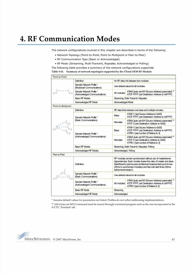
8/3/2019 Product Manual Xtend Oem Rfmodule
http://slidepdf.com/reader/full/product-manual-xtend-oem-rfmodule 43/71
© 2007
MaxStream,
Inc.
43
4. RF Communication Modes
The network configurations covered in this chapter are described in terms of the following:
• Network Topology (Point-to-Point, Point-to-Multipoint or Peer-to-Peer)
• RF Communication Type (Basic or Acknowledged)
• RF Mode (Streaming, Multi-Transmit, Repeater, Acknowledged or Polling)
The following table provides a summary of the network configurations supported.
* Assume default values for parameters not listed. Profiles do not reflect addressing implementations.
** AM (Auto‐set MY) Command must be issued through a terminal program such as the one incorporated in the X‐CTU ʹTerminalʹ tab.
Table 4‐01. Summary of network topologies supported by the XTend OEM RF Module
Point-to-Point
Definition An RF data link between two modules.
Sample Network Profile *(Broadcast Communications)
Use default values for all modules.
Sample Network Profile *(Acknowledged Communications)
All modules:ATAM [auto-set MY (Source Address) parameter] **ATDT FFFF [set Destination Address to 0xFFFF]
Basic RF Modes Streaming, Multi-Transmit, Repeater
Acknowledged RF Mode Acknowledged Mode
Point-to-Multipoint
Definition RF data links between one base and multiple remotes.
Sample Network Profile *(Basic Communications)
Base:ATMY 0 [set Source Address to 0x00]ATDT FFFF [set Destination Address to 0xFFFF]
Remotes:ATAM [auto-set MY (Source Address) parameter] **ATDT 0 [set Destination Address to 0x00]
Sample Network Profile *(Acknowledged Communications)
Base:ATMY 0 [set Source Address to 0x00]ATDT FFFF [set Destination Address to 0xFFFF]ATRR 3 [set number of Retries to 3]
Remotes:ATAM [auto-set MY (Source Address) parameter] **ATDT 0 [set Destination Address to 0x00]
ATRR 3 [set number of Retries to 3]Basic RF Modes Streaming, Multi-Transmit, Repeater, Polling
Acknowledged RF Modes Acknowledged, Polling
Peer-to-Peer
Definition
RF modules remain synchronized without use of master/server dependencies. Each module shares the roles of master and slave.MaxStream's peer-to-peer architecture features fast synch times(35ms to synchronize modules) and fast cold start times (50msbefore transmission).
Sample Network Profile *(Basic Communications)
Use default values for all modules.
Sample Network Profile *(Acknowledged Communications)
All modules:ATAM [auto-set MY (Source Address) parameter] **ATDT FFFF [set Destination Address to 0xFFFF]ATRR 3 [set number of Retries to 3]
Basic RF Mode Streaming
Acknowledged RF Mode Acknowledged
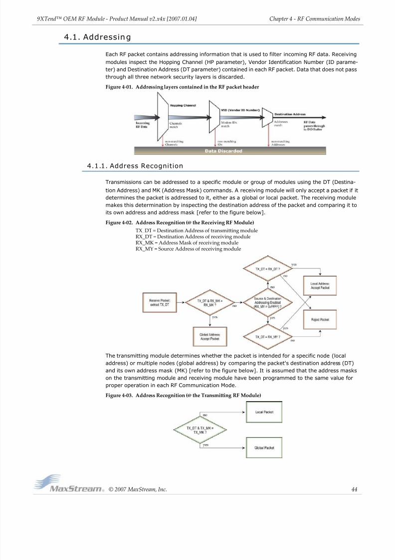
8/3/2019 Product Manual Xtend Oem Rfmodule
http://slidepdf.com/reader/full/product-manual-xtend-oem-rfmodule 44/71
9XTend™ OEM RF Module ‐ Product Manual v2.x4x [2007.01.04]
© 2007
MaxStream,
Inc.
44
Chapter 4 ‐ RF Communication Modes
4.1. Addressing
Each RF packet contains addressing information that is used to filter incoming RF data. Receiving
modules inspect the Hopping Channel (HP parameter), Vendor Identification Number (ID parame-
ter) and Destination Address (DT parameter) contained in each RF packet. Data that does not pass
through all three network security layers is discarded.
Figure 4‐01. Addressing layers contained in the RF packet header
4.1.1. Address Recognition
Transmissions can be addressed to a specific module or group of modules using the DT (Destina-
tion Address) and MK (Address Mask) commands. A receiving module will only accept a packet if it
determines the packet is addressed to it, either as a global or local packet. The receiving module
makes this determination by inspecting the destination address of the packet and comparing it to
its own address and address mask [refer to the figure below].
Figure 4‐02. Address Recognition (@ the Receiving RF Module)
TX_DT = Destination Address of transmitting module RX_DT = Destination Address of receiving module RX_MK = Address Mask of receiving module RX_MY = Source Address of receiving module
The transmitting module determines whether the packet is intended for a specific node (local
address) or multiple nodes (global address) by comparing the packet's destination address (DT)
and its own address mask (MK) [refer to the figure below]. It is assumed that the address masks
on the transmitting module and receiving module have been programmed to the same value for
proper operation in each RF Communication Mode.
Figure 4‐03. Address Recognition (@ the Transmitting RF Module)

8/3/2019 Product Manual Xtend Oem Rfmodule
http://slidepdf.com/reader/full/product-manual-xtend-oem-rfmodule 45/71
9XTend™ OEM RF Module ‐ Product Manual v2.x4x [2007.01.04]
© 2007
MaxStream,
Inc.
45
Chapter 4 ‐ RF Communication Modes
4.2. Basic Communications
Basic Communications are accomplished through two sub-types:
• Broadcast - By default, XTend RF Modules communicate through Broadcast communicationsand within a peer-to-peer network topology. When any module transmits, all other moduleswithin range will receive the data and pass it directly to their host device.
• Addressed - If addressing parameters match are in order, received RF data is forwarded to theDO (Data Out) buffer; otherwise, the RF data is discarded.
When using Basic Communications, any functions such as acknowledgements are handled at the
application layer by the OEM/integrator. The Broadcast Modes provide transparent communica-
tions, meaning that the RF link simply replaces a wired link.
4.2.1. Streaming Mode (Default)
Characteristics:Highest data throughput
Lowest latency and jitter
Reduced immunity to interference
Transmissions never acknowledged (ACK) by receiving module(s)
Required Parameter Values (TX module): RR (Retries) = 0
Related Commands: Networking (DT, MK, MY), Serial Interfacing (PK, RB, RO, TT)
Recommended Use: Mode is most appropriate for data systems more sensitive to latency and/or jitter than to occasional packet loss. For example: streaming audio or video.
Connection Sequence
Figure 4‐04. Streaming Mode State Diagram (TX Module)
• Events & processes in this mode are common to all of the other RF Modes.
• When streaming data, RB and RO parameters are onlyobserved on the first packet.
After transmission begins, the transmission event will con-
tinue uninterrupted until the DI buffer is empty or the
streaming limit (TT parameter) is reached. As with the first
packet, the payload of each subsequent packet includes up
to the maximum packet size (PK parameter).
The TT parameter (streaming limit) is specified by the TX
(transmitting) module as the maximum number of bytes the
TX module can send in one transmission event. After the TT
parameter threshold is reached, the TX module will force a
random delay of 1 to RN delay slots (exactly 1 delay slot if
RN = 0).
Subsequent packets are sent without an RF initializer since
RX (receiving) modules remain synchronized with the TX
module for the duration of the transmission (from preceding
packet information). However, due to interference, some RX
modules may lose data (and synchronization to the TX mod-
ule), particularly during long transmission events.Once the TX module has sent all pending data or has
reached the TT limit, the transmission event ends. The TX
module will not transmit again for exactly RN delay slots if
the local (i.e. TX module's) RN parameter is set to a non-
zero value. The RX module(s) will not transmit for a random
number of delay slots between 0 and (RN-1) if the local (i.e.
receiving module's) RN parameter is set to a non-zero
value. These delays are intended to lessen congestion fol-
lowing long bursts of packets from a single TX module, dur-
ing which several RX modules may have become ready to transmit.
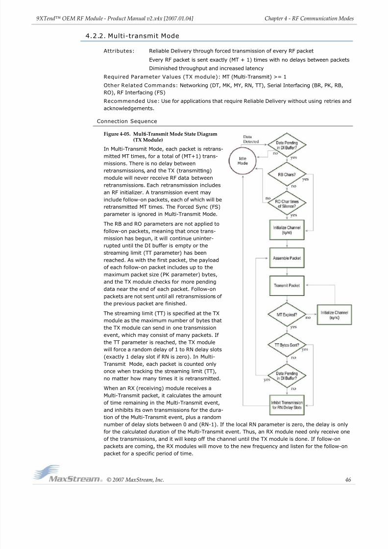
8/3/2019 Product Manual Xtend Oem Rfmodule
http://slidepdf.com/reader/full/product-manual-xtend-oem-rfmodule 46/71
9XTend™ OEM RF Module ‐ Product Manual v2.x4x [2007.01.04]
© 2007
MaxStream,
Inc.
46
Chapter 4 ‐ RF Communication Modes
4.2.2. Multi-transmit Mode
Attributes: Reliable Delivery through forced transmission of every RF packet
Every RF packet is sent exactly (MT + 1) times with no delays between packets
Diminished throughput and increased latency
Required Parameter Values (TX module): MT (Multi-Transmit) >= 1
Other Related Commands: Networking (DT, MK, MY, RN, TT), Serial Interfacing (BR, PK, RB,
RO), RF Interfacing (FS)
Recommended Use: Use for applications that require Reliable Delivery without using retries and
acknowledgements.
Connection Sequence
Figure 4‐05. Multi‐Transmit Mode State Diagram
(TX Module)
In Multi-Transmit Mode, each packet is retrans-
mitted MT times, for a total of (MT+1) trans-
missions. There is no delay between
retransmissions, and the TX (transmitting)
module will never receive RF data between
retransmissions. Each retransmission includes
an RF initializer. A transmission event mayinclude follow-on packets, each of which will be
retransmitted MT times. The Forced Sync (FS)
parameter is ignored in Multi-Transmit Mode.
The RB and RO parameters are not applied to
follow-on packets, meaning that once trans-
mission has begun, it will continue uninter-
rupted until the DI buffer is empty or the
streaming limit (TT parameter) has been
reached. As with the first packet, the payload
of each follow-on packet includes up to the
maximum packet size (PK parameter) bytes,
and the TX module checks for more pending
data near the end of each packet. Follow-onpackets are not sent until all retransmissions of
the previous packet are finished.
The streaming limit (TT) is specified at the TX
module as the maximum number of bytes that
the TX module can send in one transmission
event, which may consist of many packets. If
the TT parameter is reached, the TX module
will force a random delay of 1 to RN delay slots
(exactly 1 delay slot if RN is zero). In Multi-
Transmit Mode, each packet is counted only
once when tracking the streaming limit (TT),
no matter how many times it is retransmitted.
When an RX (receiving) module receives a
Multi-Transmit packet, it calculates the amount
of time remaining in the Multi-Transmit event,
and inhibits its own transmissions for the dura-
tion of the Multi-Transmit event, plus a random
number of delay slots between 0 and (RN-1). If the local RN parameter is zero, the delay is only
for the calculated duration of the Multi-Transmit event. Thus, an RX module need only receive one
of the transmissions, and it will keep off the channel until the TX module is done. If follow-on
packets are coming, the RX modules will move to the new frequency and listen for the follow-on
packet for a specific period of time.
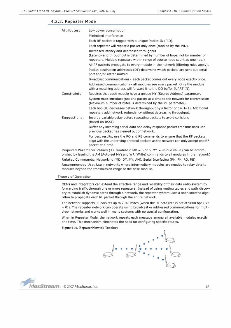
8/3/2019 Product Manual Xtend Oem Rfmodule
http://slidepdf.com/reader/full/product-manual-xtend-oem-rfmodule 47/71
9XTend™ OEM RF Module ‐ Product Manual v2.x4x [2007.01.04]
© 2007
MaxStream,
Inc.
47
Chapter 4 ‐ RF Communication Modes
4.2.3. Repeater Mode
Attributes: Low power consumption
Minimized interference
Each RF packet is tagged with a unique Packet ID (PID).
Each repeater will repeat a packet only once (tracked by the PID).
Increased latency and decreased throughput
(Latency and throughput is determined by number of hops, not by number of
repeaters. Multiple repeaters within range of source node count as one hop.)
All RF packets propagate to every module in the network (filtering rules apply).
Packet destination addresses (DT) determine which packets are sent out serial
port and/or retransmitted.
Broadcast communications - each packet comes out every node exactly once.
Addressed communications - all modules see every packet. Only the module
with a matching address will forward it to the DO buffer (UART IN).
Constraints: Requires that each module have a unique MY (Source Address) parameter.
System must introduce just one packet at a time to the network for transmission
(Maximum number of bytes is determined by the PK parameter).
Each hop (H) decreases network throughput by a factor of 1/(H+1). Additional
repeaters add network redundancy without decreasing throughput.
Suggestions: Insert a variable delay before repeating packets to avoid collisions
(based on RSSI).
Buffer any incoming serial data and delay response packet transmissions until
previous packet has cleared out of network.
For best results, use the RO and RB commands to ensure that the RF packets
align with the underlying protocol packets as the network can only accept one RF
packet at a time.
Required Parameter Values (TX module): MD = 5 or 6, MY = unique value (can be accom-
plished by issuing the AM (Auto-set MY) and WR (Write) commands to all modules in the network)
Related Commands: Networking (MD, DT, MY, AM), Serial Interfacing (RN, PK, RO, RB)
Recommended Use: Use in networks where intermediary modules are needed to relay data to
modules beyond the transmission range of the base module.
Theory of Operation
OEMs and integrators can extend the effective range and reliability of their data radio system by
forwarding traffic through one or more repeaters. Instead of using routing tables and path discov-
ery to establish dynamic paths through a network, the repeater system uses a sophisticated algo-
rithm to propagate each RF packet through the entire network.
The network supports RF packets up to 2048 bytes (when the RF data rate is set at 9600 bps (BR
= 0)). The repeater network can operate using broadcast or addressed communications for multi-
drop networks and works well in many systems with no special configuration.
When in Repeater Mode, the network repeats each message among all available modules exactly
one time. This mechanism eliminates the need for configuring specific routes.
Figure 4‐06. Repeater Network Topology

8/3/2019 Product Manual Xtend Oem Rfmodule
http://slidepdf.com/reader/full/product-manual-xtend-oem-rfmodule 48/71
9XTend™ OEM RF Module ‐ Product Manual v2.x4x [2007.01.04]
© 2007
MaxStream,
Inc.
48
Chapter 4 ‐ RF Communication Modes
Repeater Network Configuration
A network may consist of End Nodes (EN), End/Repeater Nodes (ERN) and a Base Node (BN). The
base node initiates all communications.
A repeater network can be configured to operate using Basic Broadcast or Basic Addressed com-
munications. The addressing capabilities of the module allow integrators to send a packet as a glo-
bal packet (DT = 0xFFFF) and shift out of every module in the network (Basic Broadcast).
Alternatively, the packet can be sent with a specific DT (Destination Address) parameter so that it
is only accepted by a specific remote node (Basic Addressed).Configuration Instruction (Basic Broadcast Communications)
The configuration instructions above reflect configuration for a Basic Broadcast Repeater system.
To configure a Basic Addressed Repeater system, use the DT (Destination Address) parameter toassign unique addresses to each module in the network.
Algorithm Details
• Packet ID (PID) is composed of TX (transmitting) module MY address and packet sequencenumber.
• Incoming packets with a PID already found in the PID buffer will be ignored.
• Each module maintains a PID buffer 4 deep of previously received packets (managed asFIFO).
Packets may be shifted out the serial port and/or repeated depending on the DT parameter con-
tained in the RF packet.
Repeat Delay Based on RSSI
A transmitted packet may be received by more that one repeater at the same time. In order to
reduce the probability that the repeaters will transmit at the same instant, resulting in a collision
and possible data loss; an algorithm has been developed that will allow a variable back-off prior to
retransmission of the packet by a repeater. The algorithm allows radios that receive the packet
with a stronger RF signal (RSSI) to have the first opportunity to retransmit the packet.
The RN (Delay Slots) parameter is used to configure this delay. Set RN=0 (no delays) for small
networks with few repeaters or repeaters that are not within range of each other. Set RN=1 for
systems with 2 to 5 repeaters that may be within range of each other.
The actual length of the delay is computed by the formula:
Delay (ms) = L * DS
DS = (-41-RSSI)/10*RN)+RandomInt(0,RN)
Where L is the length of the transmitted packet in milliseconds, DS is the number of delay slots to
wait, RSSI is the received signal strength in dBm, RN is the value of the RN register and Random-
Int(A,B) is a function that returns a random integer from A to B-0
Assign each module a unique MY (source) address. (The AM (Auto-set MY) command will con-
figure a unique source address that is based on module serial number.)
Enable Basic Broadcast Communications (DT = 0xFFFF) or Addressed Broadcast Communica-
tions (DT specifies a specific destination)
Configure PK, RO and RB to ensure that RF packet aligns with protocol packet. (ex. PK=0x100,
RB=0x100, RO depends on baud rate).
Configure one or more repeaters in the system (MD = 5).
Configure remote nodes as destinations (MD = 6). This will ensure that the remote node waits
for the repeater traffic to subside before it transmits a response.
Table 4‐02. DT (Destination Address) parameter truth table
Address Match Send out serial port? Repeat?
Global Yes YesLocal Yes No
None No Yes
8/3/2019 Product Manual Xtend Oem Rfmodule
http://slidepdf.com/reader/full/product-manual-xtend-oem-rfmodule 49/71
9XTend™ OEM RF Module ‐ Product Manual v2.x4x [2007.01.04]
© 2007
MaxStream,
Inc.
49
Chapter 4 ‐ RF Communication Modes
Response Packet Delay
As a packet propagates through the repeater network, if any node receives the data and generates
a quick response, the response needs to be delayed so as not to collide with subsequent retrans-
missions of the original packet. To reduce collisions, both repeater and end node radios in a
repeater network will delay transmission of data shifted in the serial port to allow any repeaters
within range to complete their retransmissions.
The time for this delay is computed by the formula:
Maximum Delay (ms) = L * DSDS = ((-41-(-100))/10)*RN)+RN+1
Where L is the length of the transmitted packet in milliseconds, DS is the number of delay slots to
wait, RSSI is the received signal strength in dBm, and RN is the value of the RN register.
Use Case - Broadcast Repeater Network
Consider modules R1 through R10 each communicating to a PLC using the ModBus protocol and
spaced evenly in a line. All ten modules are configured as 'destinations & repeaters' within the
scope of Basic Broadcast Communications (MD=5, AM, DT=0xFFFF, PK=0x100, RO=0x03,
RB=0x100, RN=1). The Base Host (BH) shifts payload that is destined for R10 to R1. R1 initializes
RF communication and transmits payload to nodes R2 through R5 which are all within range of R1.
The modules R2 through R5 receive the RF packet and retransmit the packet simultaneously. They
also send the data out the serial ports, to the PLCs.
Bandwidth Considerations
Using broadcast repeaters in a network reduces the overall network data throughput as each
repeater must buffer an entire packet before retransmitting it. For example: if the destination iswithin range of the transmitter and the packet is 32-bytes long, the transmission will take 12ms on
an XTend module operating at 115,200 baud. If the same packet must propagate through two
repeaters, it will take 12ms to arrive at the first repeater, 12ms to get to the second and a final
12ms to reach the destination for a total of 36ms. Taking into account UART transfer times (~1ms/
byte at 9600 baud), a server to send a 32-byte query and receive a 32-byte response is about
200ms, allowing for 5 polls per second. With the two repeaters in the path, the same query/
response sequence would take about 500ms for 2 polls per second.
Generally, network throughput will decrease by a factor of 1/(R+1), with R representing the num-
ber of repeaters between the source and destination.
Table 4‐03. Commands used to configure repeater functions
AT
Command
Binary
Command
AT Command
NameRange
# Bytes
Returned
Factory
Default
AM 0x3A (58d) Auto-set MY - - -
DT 0x00 (0d) Destination Address 0 - 0xFFFF 2 0
MD 0x3C (60d) RF Mode 0 - 6 1 0
MY 0x2A (42d) Source Address 0 - 0xFFFF 2 0xFFFF
RN 0x19 (25d) Delay Slots 0 - 0xFF [slots] 1 0
WR 0x08 (8d) Write - - -
8/3/2019 Product Manual Xtend Oem Rfmodule
http://slidepdf.com/reader/full/product-manual-xtend-oem-rfmodule 50/71
9XTend™ OEM RF Module ‐ Product Manual v2.x4x [2007.01.04]
© 2007
MaxStream,
Inc.
50
Chapter 4 ‐ RF Communication Modes
4.2.4. Polling Mode (Basic)
NOTE: Polling Mode (Basic) and Polling Mode (Acknowledged) [p53] operate in the same way. The
only difference between the two modes is in their means of achieving reliable delivery of data. In
Polling Mode (Basic), reliable delivery is achieved using multiple transmissions.
Attributes: Utilizes high percentage of available network bandwidth
Eliminates collisions
Works with reliable delivery (RR or MT parameters)Supports binary data transfers
Base module requests packets from remote module by polling a sequential
range of addresses
Base module is configured to specify the range of addresses being polled
Uses inter-character delay to create RF packet lengths aligned with protocol
packet lengths up to 2048 bytes long.
Required Parameter Values (Base): MD (RF Mode) = 3, PB (Polling Begin Address), PE (Polling
End Address)
Required Parameter Value (Remote): MD (RF Mode) = 4
Related Commands: Networking (MT, PD, DT, MY, AM)
Constraints: The minimum time interval between polling cycles is configurable. However, if the
remote modules cannot all be processed within that time interval, the polling cycle is ineffective(i.e. it will impose no additional delay). In order to ensure a pause between polling cycles, PD
must be set to a value which is large enough to accommodate the pause.
Recommended Use: Use for point-to-multipoint applications that require Reliable Delivery of
data. Use this mode when it is critical that a base module be able to discern data coming from
multiple modules.
Theory of Operation
A ‘Polling Base’ module will cycle through a sequential range of addresses. The ‘Polling Base’ will
poll each ‘Polling Remote’ module, wait for a response, then poll the next remote address in the
sequence. Each ‘Polling Remote’ will respond by sending the data from its DI (Data In) buffer fol-
lowing the RB (Packetization Threshold) & RO (Packetization Timeout) parameters. When there is
no eligible data to send, the ‘Polling Remote’ will not respond. The ‘Polling Base’ will poll the next
address in the polling sequence after a short delay.
Polling Base Configuration:
Polling Remote Configuration:
Set the MD (RF Mode) parameter (MD = 3).
Set MY (Source Address) parameter (MY = 0).
Set the sequential range of Polling Addresses using the PB (Polling Begin Address) and PE
(Polling End Address) parameters.
(Optional) Enable Basic Reliable Delivery (MT >= 0). Note: Acknowledged Reliable Delivery is
also supported. Refer to the ‘Polling Mode - Acknowledged’ section for more information.
(Optional) Use the PD (Minimum Polling Delay) command to configure a delay between polls to
slow down system (if needed).
(Optional) Enable API Mode to address remotes within polling range on a packet-by-packet
basis.
Set the MD (RF Mode) parameter (MD = 4).
Configure sequential source addresses for all remote modules using the MY (Source Address)
command.
Set the DT (Destination Address) parameter to point to ‘Polling Base’ (DT = 0x0000).
(Optional) Enable Basic Reliable Delivery (MT >= 0). Note: Acknowledged Reliable Delivery is
also supported. Refer to the ‘Polling Mode - Acknowledged’ section for more information.

8/3/2019 Product Manual Xtend Oem Rfmodule
http://slidepdf.com/reader/full/product-manual-xtend-oem-rfmodule 51/71
9XTend™ OEM RF Module ‐ Product Manual v2.x4x [2007.01.04]
© 2007
MaxStream,
Inc.
51
Chapter 4 ‐ RF Communication Modes
4.3. Acknow ledged Communications
4.3.1. Acknowledged Mode
Attributes: Reliable delivery through positive acknowledgements for each packet
Throughput, latency and jitter vary depending on the quality of the channel and
the strength of the signal.
Required Parameter Values (TX module): RR (Retries) >= 1
Related Commands: Networking (DT, MK, RR), Serial Interfacing (PK, RN, RO, RB, TT)
Recommended Use: Use for applications that require Reliable Delivery. If messages are smaller
than 256 bytes, use RB and RO commands to align RF packets to application packets.
Connection Sequence
Figure 4‐07. Acknowledged Mode State
Diagram (TX module)
After sending a packet while in
Acknowledged Mode, the TX (trans-
mitting) module listens for an ACK
(acknowledgement). If it receives
the ACK, it will either move on tosending a subsequent packet (if
more transmit data is pending) or
will wait for exactly RN random delay
slots before allowing another trans-
mission (if no more data is pending
to be transmitted).
If the TX module does not receive
the ACK within the allotted time, it
will retransmit the packet with a new
RF initializer following the ACK slot.
There is no delay between the first
ACK slot and the first retransmission.
Subsequent retransmissions incur adelay of a random number of delay
slots, between 0 and RN. If RN is set
to 0 on the TX module, there are
never any back-off delays between
retransmissions. Note that during
back-off delays, the TX module will
go into Idle Mode and may receive
RF data. This can have the effect of
increasing the back-off delay, as the
module cannot return to Transmit (or
retransmit) Mode as long as it is receiving RF data.
After receiving and acknowledging a packet, the RX (receiving) module will move to the next fre-
quency and listen for either a retransmission or new data for a specific period of time. Even if theTX module has indicated that it has no more pending transmit data, it may not have received the
previous ACK, and so may retransmit the packet, possibly with no delay after the ACK slot. In this
case, the RX module will always detect the immediate retransmission, which will hold off the com-
munications channel and thereby reduce collisions. RX modules acknowledge each retransmission
they receive, but they only pass the first copy of a packet they receive out the UART.
RB and RO parameters are not applied to subsequent packets, meaning that once transmission
has begun, it will continue uninterrupted until the DI buffer is empty or the streaming limit (TT
parameter) has been reached. As with the first packet, the payload of each subsequent packet
includes up to the maximum packet size (PK parameter), and the TX module checks for more
pending data near the end of each packet.

8/3/2019 Product Manual Xtend Oem Rfmodule
http://slidepdf.com/reader/full/product-manual-xtend-oem-rfmodule 52/71
9XTend™ OEM RF Module ‐ Product Manual v2.x4x [2007.01.04]
© 2007
MaxStream,
Inc.
52
Chapter 4 ‐ RF Communication Modes
The TT parameter (streaming limit) specifies the maximum number of bytes that the TX module
will send in one transmission event, which may consist of many packets and retries. If the TT
parameter is reached, the TX module will force a random delay of 1 to RN delay slots (exactly 1
delay slot if RN is zero). Each packet is counted only once toward TT, no matter how many times
the packet is retransmitted.
Subsequent packets in Acknowledged Mode are similar to those in Streaming Mode, with the addi-
tion of an ACK between each packet, and the possibility of retransmissions. Subsequent packets
are sent without an RF initializer, as the RX modules are already synchronized to the TX module
from the preceding packet(s) and they remain synchronized for the duration of the transmission
event. Each retransmission of a packet includes an RF initializer.
Once the TX module has sent all pending data or has reached the TT limit, the acknowledged
transmission event is completed. The TX module will not transmit again for exactly RN delay slots,
if the local RN parameter is set to a non-zero value. The RX module will not transmit for a random
number of delay slots between 0 and (RN-1), if the local RN parameter is set to a non-zero value.
These delays are intended to lessen congestion following long bursts of packets from a single TX
module, during which several RX modules may have themselves become ready to transmit.

8/3/2019 Product Manual Xtend Oem Rfmodule
http://slidepdf.com/reader/full/product-manual-xtend-oem-rfmodule 53/71
9XTend™ OEM RF Module ‐ Product Manual v2.x4x [2007.01.04]
© 2007
MaxStream,
Inc.
53
Chapter 4 ‐ RF Communication Modes
4.3.2. Polling Mode (Acknow ledged)
NOTE: Polling Mode (Acknowledged) and Polling Mode (Basic) [p50] operate in the same way. The
difference between the two modes is in their means of achieving reliable delivery of data. In Poll-
ing Mode (Acknowledged), reliable delivery is achieved using retries and acknowledgements.
Attributes: Utilizes high percentage of available network bandwidth
Eliminates collisions
Works with reliable delivery (RR or MT parameters)
Supports binary data transfers
Base module requests packets from remote module by polling a sequential
range of addresses
Base module is configured to specify the range of addresses being polled
Uses inter-character delay to create RF packet lengths aligned with protocol
packet lengths up to 2048 bytes long.
Required Parameter Values (Base): MD (RF Mode) = 3, PB (Polling Begin Address), PE (Polling
End Address)
Required Parameter Values (Remote): MD (RF Mode) = 4
Related Commands: Networking (RR, PD, DT, MY, AM)
Constraints: The minimum time interval between polling cycles is configurable. However, if the
remote modules cannot all be processed within that time interval, the polling cycle is ineffective
(i.e. it will impose no additional delay). In order to ensure a pause between polling cycles, PD
must be set to a value which is large enough to accommodate the pause.
Recommended Use: Use for point-to-multipoint applications that require Reliable Delivery of
data. Use this mode when it is critical that a base module be able to discern data coming from
multiple modules.
Theory of Operation
A ‘Polling Base’ module will cycle through a sequential range of addresses. The ‘Polling Base’ will
poll each ‘Polling Remote’ module, wait for a response, then poll the next remote address in the
sequence. Each ‘Polling Remote’ will respond by sending the data from its DI (Data In) buffer fol-
lowing the RB (Packetization Threshold) & RO (Packetization Timeout) parameters. When there is
no eligible data to send, the ‘Polling Remote’ will not respond. The ‘Polling Base’ will poll the next
address in the polling sequence after a short delay.
Polling Base Configuration:
Polling Remote Configuration:
Set the MD (RF Mode) parameter (MD = 3).
Set MY (Source Address) parameter (MY = 0).
Set the sequential range of Polling Addresses using the PB (Polling Begin Address) and PE
(Polling End Address) parameters.
(Optional) Enable Acknowledged Reliable Delivery (RR >= 0). Note: Basic Reliable Delivery is
also supported. Refer to the ‘Polling Mode - Basic section for more information.
(Optional) Use the PD (Minimum Polling Delay) command to configure a delay between polls to
slow down system (if needed).
(Optional) Enable API Mode to address remotes within polling range on a packet-by-packet
basis.
Set the MD (RF Mode) parameter (MD = 4).
Configure sequential source addresses for all remote modules using the MY (Source Address)
command.
Set the DT (Destination Address) parameter to point to ‘Polling Base’ (DT = 0x0000).
(Optional) Enable Acknowledged Reliable Delivery (RR >= 0). Note: Basic Reliable Delivery is
also supported. Refer to the ‘Polling Mode - Basic section for more information.
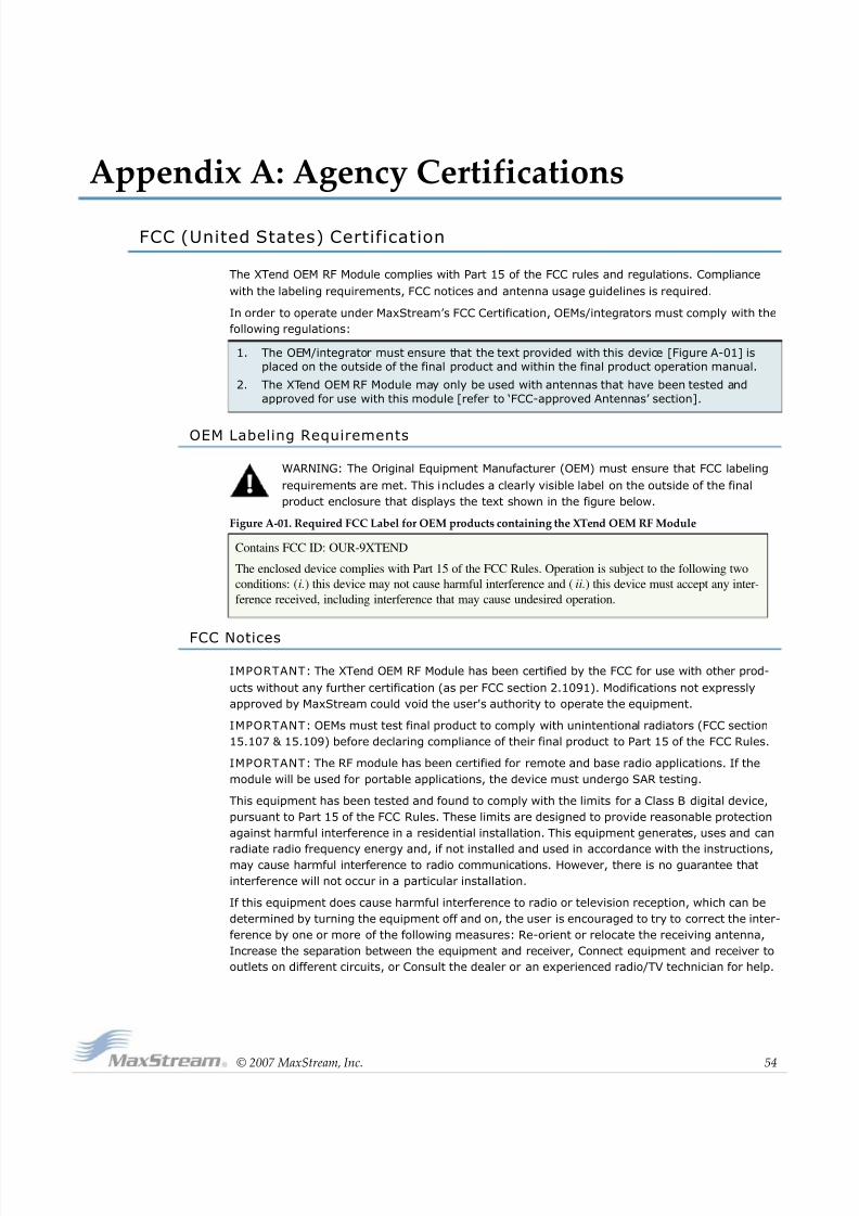
8/3/2019 Product Manual Xtend Oem Rfmodule
http://slidepdf.com/reader/full/product-manual-xtend-oem-rfmodule 54/71
© 2007
MaxStream,
Inc.
54
Appendix A: Agency Certifications
FCC (United States) Certification
The XTend OEM RF Module complies with Part 15 of the FCC rules and regulations. Compliance
with the labeling requirements, FCC notices and antenna usage guidelines is required.
In order to operate under MaxStream’s FCC Certification, OEMs/integrators must comply with the
following regulations:
OEM Labeling Requirements
WARNING: The Original Equipment Manufacturer (OEM) must ensure that FCC labeling
requirements are met. This includes a clearly visible label on the outside of the final
product enclosure that displays the text shown in the figure below.
Figure A‐01. Required FCC Label for OEM products containing the XTend OEM RF Module
FCC Notices
IMPORTANT: The XTend OEM RF Module has been certified by the FCC for use with other prod-
ucts without any further certification (as per FCC section 2.1091). Modifications not expressly
approved by MaxStream could void the user's authority to operate the equipment.
IMPORTANT: OEMs must test final product to comply with unintentional radiators (FCC section
15.107 & 15.109) before declaring compliance of their final product to Part 15 of the FCC Rules.
IMPORTANT: The RF module has been certified for remote and base radio applications. If the
module will be used for portable applications, the device must undergo SAR testing.
This equipment has been tested and found to comply with the limits for a Class B digital device,
pursuant to Part 15 of the FCC Rules. These limits are designed to provide reasonable protection
against harmful interference in a residential installation. This equipment generates, uses and can
radiate radio frequency energy and, if not installed and used in accordance with the instructions,may cause harmful interference to radio communications. However, there is no guarantee that
interference will not occur in a particular installation.
If this equipment does cause harmful interference to radio or television reception, which can be
determined by turning the equipment off and on, the user is encouraged to try to correct the inter-
ference by one or more of the following measures: Re-orient or relocate the receiving antenna,
Increase the separation between the equipment and receiver, Connect equipment and receiver to
outlets on different circuits, or Consult the dealer or an experienced radio/TV technician for help.
1. The OEM/integrator must ensure that the text provided with this device [Figure A-01] is
placed on the outside of the final product and within the final product operation manual.
2. The XTend OEM RF Module may only be used with antennas that have been tested and
approved for use with this module [refer to ‘FCC-approved Antennas’ section].
Contains FCC ID: OUR-9XTEND
The enclosed device complies with Part 15 of the FCC Rules. Operation is subject to the following two
conditions: (i.) this device may not cause harmful interference and (ii.) this device must accept any inter-
ference received, including interference that may cause undesired operation.
8/3/2019 Product Manual Xtend Oem Rfmodule
http://slidepdf.com/reader/full/product-manual-xtend-oem-rfmodule 55/71
9XTend™ OEM RF Module ‐ Product Manual v2.x4x [2007.01.04]
© 2007
MaxStream,
Inc.
55
Appendix A: Agency Certifications
Limited Modular Approval
Power output is conducted at the antenna terminal and can be adjusted from 1 mill-watt to 1 Watt
at the OEM level. This is an RF module approved for Limited Modular use operating as a mobile
transmitting device with respect to section 2.1091 and is limited to OEM installation for Mobile and
Fixed applications only. During final installation, end-users are prohibited from access to any pro-
gramming parameters. Professional installation adjustment is required for setting module power
and antenna gain to meet EIRP compliance for high gain antenna(s).
Final antenna installation and operating configurations of this transmitter including antenna gain
and cable loss must not exceed the EIRP of the configuration used for calculating MPE. Grantee
(MaxStream) must coordinate with OEM integrators to ensure the end-users and installers of prod-
ucts operating with the module are provided with operating instructions to satisfy RF exposure
requirements.
The FCC grant is valid only when the device is sold to OEM integrators. Integrators are instructed
to ensure the end-user has no manual instructions to remove, adjust or install the device.
FCC-approved Antennas
WARNING: This device has been tested with Reverse Polarity SMA connectors with the
antennas listed in the tables of this section. When integrated into OEM products, fixed
antennas require installation preventing end-users from replacing them with non-
approved antennas. Antennas not listed in the tables must be tested to comply with FCCSection 15.203 (unique antenna connectors) and Section 15.247 (emissions).
Fixed Base Station and Mobile Applications
MaxStream RF Modules are pre-FCC approved for use in fixed base station and mobile applica-
tions. When the antenna is mounted at least 20cm (8") from nearby persons, the application is
considered a mobile application.
Portable Applications and SAR Testing
When the antenna is mounted closer than 20cm to nearby persons, then the application is consid-
ered "portable" and requires an additional test be performed on the final product. This test is
called Specific Absorption Rate (SAR) testing and measures the emissions from the module and
how they affect the person.
RF Exposure
This statement must be included as a CAUTION statement in OEM product manuals.
WARNING: This equipment is approved only for mobile and base station transmitting
devices. Antenna(s) used for this transmitter must be installed to provide a separation
distance of at least 30 cm from all persons and must not be co-located or operating in
conjunction with any other antenna or transmitter.
NOTE: The separation distance indicated in the above is 30 cm, but any distance greater than or
equal to 23 cm can be used (per MPE evaluation).
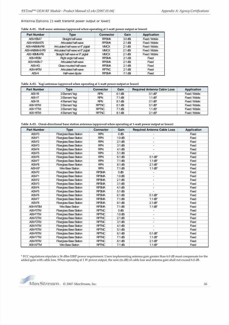
8/3/2019 Product Manual Xtend Oem Rfmodule
http://slidepdf.com/reader/full/product-manual-xtend-oem-rfmodule 56/71
9XTend™ OEM RF Module ‐ Product Manual v2.x4x [2007.01.04]
© 2007
MaxStream,
Inc.
56
Appendix A: Agency Certifications
Antenna Options (1-watt transmit power output or lower)
Table A‐01. Half‐wave antennas (approved when operating at 1‐watt power output or lower)
* FCC regulations stipulate a 36 dBm EIRP power requirement. Users implementing antenna gain greater than 6.0 dB must compensate for the added gain with cable loss. When operating at 1 W power output, the sum (in dB) of cable loss and antenna gain shall not exceed 6.0 dB.
Part Number Type Connector Gain Application
A09-HSM-7 Straight half-wave RPSMA 3.0 dBi Fixed / Mobile
A09-HASM-675 Articulated half-wave RPSMA 2.1 dBi Fixed / Mobile
A09-HABMM-P6I Articulated half-wave w/ 6" pigtail MMCX 2.1 dBi Fixed / Mobile
A09-HABMM-6-P6I Articulated half-wave w/ 6" pigtail MMCX 2.1 dBi Fixed / Mobile
A09-HBMM-P6I Straight half-wave w/ 6" pigtail MMCX 2.1 dBi Fixed / Mobile
A09-HRSM Right angle half-wave RPSMA 2.1 dBi Fixed
A09-HASM-7 Articulated half-wave RPSMA 2.1 dBi Fixed
A09-HG Glass mounted half-wave RPSMA 2.1 dBi Fixed
A09-HATM Articulated half-wave RPTNC 2.1 dBi Fixed
A09-H Half-wave dipole RPSMA 2.1 dBi Fixed
Table A‐02. Yagi antennas (approved when operating at 1‐watt power output or lower)
Part Number Type Connector Gain Required Antenna Cable Loss Application
A09-Y6 2 Element Yagi RPN 6.1 dBi 0.1 dB* Fixed / Mobile
A09-Y7 3 Element Yagi RPN 7.1 dBi 1.1 dB* Fixed / Mobile
A09-Y8 4 Element Yagi RPN 8.1 dBi 2.1 dB* Fixed / Mobile
A09-Y6TM 2 Element Yagi RPTNC 6.1 dBi 0.1 dB* Fixed / Mobile
A09-Y7TM 3 Element Yagi RPTNC 7.1 dBi 1.1 dB* Fixed / Mobile
A09-Y8TM 4 Element Yagi RPTNC 8.1 dBi 2.1 dB* Fixed / Mobile
Table A‐03. Omni‐directional base station antennas (approved when operating at 1‐watt power output or lower)
Part Number Type Connector Gain Required Antenna Cable Loss Application
A09-F0 Fiberglass Base Station RPN 0 dBi - Fixed
A09-F1 Fiberglass Base Station RPN 1.0 dBi - Fixed
A09-F2 Fiberglass Base Station RPN 2.1 dBi - Fixed
A09-F3 Fiberglass Base Station RPN 3.1 dBi - Fixed
A09-F4 Fiberglass Base Station RPN 4.1 dBi - Fixed
A09-F5 Fiberglass Base Station RPN 5.1 dBi - Fixed
A09-F6 Fiberglass Base Station RPN 6.1 dBi 0.1 dB* Fixed
A09-F7 Fiberglass Base Station RPN 7.1 dBi 1.1 dB* Fixed
A09-F8 Fiberglass Base Station RPN 8.1 dBi 2.1 dB* Fixed
A09-W7 Wire Base Station RPN 7.1 dBi 1.1 dB* Fixed
A09-F0 Fiberglass Base Station RPSMA 0 dBi - Fixed
A09-F1 Fiberglass Base Station RPSMA 1.0 dBi - Fixed
A09-F2 Fiberglass Base Station RPSMA 2.1 dBi - Fixed
A09-F3 Fiberglass Base Station RPSMA 3.1 dBi - Fixed
A09-F4 Fiberglass Base Station RPSMA 4.1 dBi - Fixed
A09-F5 Fiberglass Base Station RPSMA 5.1 dBi - Fixed
A09-F6 Fiberglass Base Station RPSMA 6.1 dBi 0.1 dB* Fixed
A09-F7 Fiberglass Base Station RPSMA 7.1 dBi 1.1 dB* Fixed
A09-F8 Fiberglass Base Station RPSMA 8.1 dBi 2.1 dB* Fixed
A09-W7SM Wire Base Station RPSMA 7.1 dBi 1.1 dB* Fixed
A09-F0TM Fiberglass Base Station RPTNC 0 dBi - Fixed
A09-F1TM Fiberglass Base Station RPTNC 1.0 dBi - Fixed
A09-F2TM Fiberglass Base Station RPTNC 2.1 dBi - Fixed
A09-F3TM Fiberglass Base Station RPTNC 3.1 dBi - Fixed
A09-F4TM Fiberglass Base Station RPTNC 4.1 dBi - Fixed
A09-F5TM Fiberglass Base Station RPTNC 5.1 dBi - Fixed
A09-F6TM Fiberglass Base Station RPTNC 6.1 dBi 0.1 dB* Fixed
A09-F7TM Fiberglass Base Station RPTNC 7.1 dBi 1.1 dB* Fixed
A09-F8TM Fiberglass Base Station RPTNC 8.1 dBi 2.1 dB* Fixed
A09-W7TM Wire Base Station RPTNC 7.1 dBi 1.1 dB* Fixed
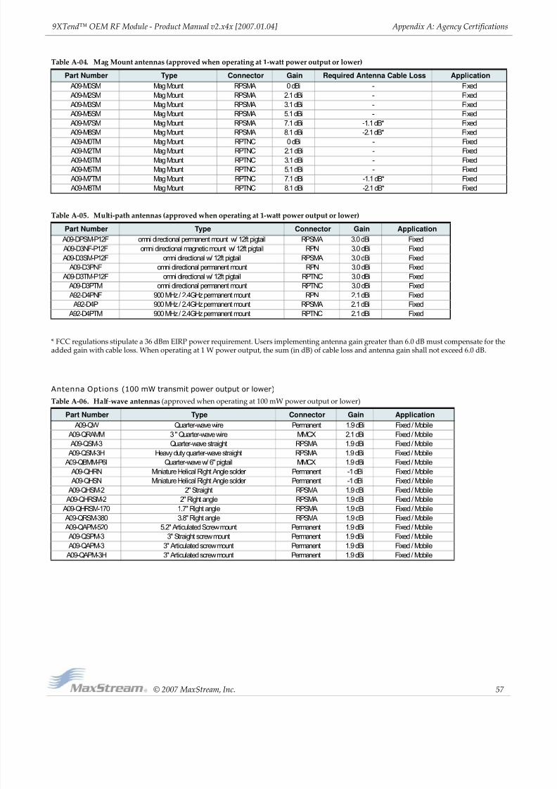
8/3/2019 Product Manual Xtend Oem Rfmodule
http://slidepdf.com/reader/full/product-manual-xtend-oem-rfmodule 57/71
9XTend™ OEM RF Module ‐ Product Manual v2.x4x [2007.01.04]
© 2007
MaxStream,
Inc.
57
Appendix A: Agency Certifications
* FCC regulations stipulate a 36 dBm EIRP power requirement. Users implementing antenna gain greater than 6.0 dB must compensate for the added gain with cable loss. When operating at 1 W power output, the sum (in dB) of cable loss and antenna gain shall not exceed 6.0 dB.
Antenna Options (100 mW transmit power output or lower)
Table A‐04. Mag Mount antennas (approved when operating at 1‐watt power output or lower)
Part Number Type Connector Gain Required Antenna Cable Loss Application
A09-M0SM Mag Mount RPSMA 0 dBi - Fixed
A09-M2SM Mag Mount RPSMA 2.1 dBi - Fixed
A09-M3SM Mag Mount RPSMA 3.1 dBi - Fixed
A09-M5SM Mag Mount RPSMA 5.1 dBi - Fixed
A09-M7SM Mag Mount RPSMA 7.1 dBi -1.1 dB* Fixed
A09-M8SM Mag Mount RPSMA 8.1 dBi -2.1 dB* Fixed
A09-M0TM Mag Mount RPTNC 0 dBi - Fixed
A09-M2TM Mag Mount RPTNC 2.1 dBi - Fixed
A09-M3TM Mag Mount RPTNC 3.1 dBi - Fixed
A09-M5TM Mag Mount RPTNC 5.1 dBi - Fixed
A09-M7TM Mag Mount RPTNC 7.1 dBi -1.1 dB* Fixed
A09-M8TM Mag Mount RPTNC 8.1 dBi -2.1 dB* Fixed
Table A‐05. Multi‐path antennas (approved when operating at 1‐watt power output or lower)
Part Number Type Connector Gain Application
A09-DPSM-P12F omni directional permanent mount w/ 12ft pigtail RPSMA 3.0 dBi Fixed
A09-D3NF-P12F omni directional magnetic mount w/ 12ft pigtail RPN 3.0 dBi Fixed
A09-D3SM-P12F omni directional w/ 12ft pigtail RPSMA 3.0 dBi Fixed
A09-D3PNF omni directional permanent mount RPN 3.0 dBi Fixed
A09-D3TM-P12F omni directional w/ 12ft pigtail RPTNC 3.0 dBi FixedA09-D3PTM omni directional permanent mount RPTNC 3.0 dBi Fixed
A92-D4PNF 900 MHz / 2.4GHz permanent mount RPN 2.1 dBi Fixed
A92-D4P 900 MHz / 2.4GHz permanent mount RPSMA 2.1 dBi Fixed
A92-D4PTM 900 MHz / 2.4GHz permanent mount RPTNC 2.1 dBi Fixed
Table A‐06. Half‐wave antennas (approved when operating at 100 mW power output or lower)
Part Number Type Connector Gain ApplicationA09-QW Quarter-wave wire Permanent 1.9 dBi Fixed / Mobile
A09-QRAMM 3 " Quarter-wave wire MMCX 2.1 dBi Fixed / Mobile
A09-QSM-3 Quarter-wave straight RPSMA 1.9 dBi Fixed / Mobile
A09-QSM-3H Heavy duty quarter-wave straight RPSMA 1.9 dBi Fixed / Mobile
A09-QBMM-P6I Quarter-wave w/ 6" pigtail MMCX 1.9 dBi Fixed / Mobile
A09-QHRN Miniature Helical Right Angle solder Permanent -1 dBi Fixed / Mobile
A09-QHSN Miniature Helical Right Angle solder Permanent -1 dBi Fixed / Mobile
A09-QHSM-2 2" Straight RPSMA 1.9 dBi Fixed / Mobile
A09-QHRSM-2 2" Right angle RPSMA 1.9 dBi Fixed / Mobile
A09-QHRSM-170 1.7" Right angle RPSMA 1.9 dBi Fixed / Mobile
A09-QRSM-380 3.8" Right angle RPSMA 1.9 dBi Fixed / Mobile
A09-QAPM-520 5.2" Articulated Screw mount Permanent 1.9 dBi Fixed / Mobile
A09-QSPM-3 3" Straight screw mount Permanent 1.9 dBi Fixed / Mobile
A09-QAPM-3 3" Articulated screw mount Permanent 1.9 dBi Fixed / Mobile
A09-QAPM-3H 3" Articulated screw mount Permanent 1.9 dBi Fixed / Mobile

8/3/2019 Product Manual Xtend Oem Rfmodule
http://slidepdf.com/reader/full/product-manual-xtend-oem-rfmodule 58/71
9XTend™ OEM RF Module ‐ Product Manual v2.x4x [2007.01.04]
© 2007
MaxStream,
Inc.
58
Appendix A: Agency Certifications
IC (Industry Canada) Certification
Labeling Requirements
Labeling requirements for Industry Canada are similar to those of the FCC. A clearly visible label
on the outside of the final product enclosure must display the following text:
Contains Model 9XTend Radio, IC: 4214A-9XTEND
The integrator is responsible for its product to comply with IC ICES-003 & FCC Part 15, Sub. B -Unintentional Radiators. ICES-003 is the same as FCC Part 15 Sub. B and Industry Canada accepts
FCC test report or CISPR 22 test report for compliance with ICES-003.
C-TICK (Australia) Certification
Pow er Requirements
Regulations in Australia stipulate a maximum of 30 dBm EIRP (Effective Isotropic Radiated Power).
The EIRP equals the sum (in dBm) of power output, antenna gain and cable loss and cannot not
exceed 30 dBm.
Figure A‐02. EIRP Formula for Australia
NOTE: The maximum EIRP for the FCC (United States) and IC (Canada) is 36 dBm.
Table A‐07. Yagi antennas (approved when operating at 100 mW power output or lower)
Part Number Type Connector Gain Application
A09-Y6 2 Element Yagi RPN 6.1 dBi Fixed / Mobile
A09-Y7 3 Element Yagi RPN 7.1 dBi Fixed / Mobile
A09-Y8 4 Element Yagi RPN 8.1 dBi Fixed / Mobile
A09-Y9 4 Element Yagi RPN 9.1 dBi Fixed / Mobile
A09-Y10 5 Element Yagi RPN 10.1 dBi Fixed / Mobile
A09-Y11 6 Element Yagi RPN 11.1 dBi Fixed / Mobile
A09-Y12 7 Element Yagi RPN 12.1 dBi Fixed / MobileA09-Y13 9 Element Yagi RPN 13.1 dBi Fixed / Mobile
A09-Y14 10 Element Yagi RPN 14.1 dBi Fixed / Mobile
A09-Y14 12 Element Yagi RPN 14.1 dBi Fixed / Mobile
A09-Y15 13 Element Yagi RPN 15.1 dBi Fixed / Mobile
A09-Y15 15 Element Yagi RPN 15.1 dBi Fixed / Mobile
A09-Y6TM 2 Element Yagi RPTNC 6.1 dBi Fixed / Mobile
A09-Y7TM 3 Element Yagi RPTNC 7.1 dBi Fixed / Mobile
A09-Y8TM 4 Element Yagi RPTNC 8.1 dBi Fixed / Mobile
A09-Y9TM 4 Element Yagi RPTNC 9.1 dBi Fixed / Mobile
A09-Y10TM 5 Element Yagi RPTNC 10.1 dBi Fixed / Mobile
A09-Y11TM 6 Element Yagi RPTNC 11.1 dBi Fixed / Mobile
A09-Y12TM 7 Element Yagi RPTNC 12.1 dBi Fixed / Mobile
A09-Y13TM 9 Element Yagi RPTNC 13.1 dBi Fixed / Mobile
A09-Y14TM 10 Element Yagi RPTNC 14.1 dBi Fixed / Mobile
A09-Y14TM 12 Element Yagi RPTNC 14.1 dBi Fixed / MobileA09-Y15TM 13 Element Yagi RPTNC 15.1 dBi Fixed / Mobile
A09-Y15TM 15 Element Yagi RPTNC 15.1 dBi Fixed / Mobile

8/3/2019 Product Manual Xtend Oem Rfmodule
http://slidepdf.com/reader/full/product-manual-xtend-oem-rfmodule 59/71
© 2007
MaxStream,
Inc.
59
Appendix B: Development Guide
Development Kit Contents
The 9XTend Development Kit includes the hardware and software needed to rapidly create long
range wireless links between devices.
Interfacing Hardware
The XTend Development Kit includes a pair of RS-232 interface boards that supports the RS-232/
485/422 protocols. When the modules are mounted to the interface boards, the boards provide
the following development tools:
• Fast and direct connection to serial devices (such as PCs) and therefore easy access to themodule registries - The parameters stored in the registry allow OEMs and integrators to cus-tomize the modules to suite the specific needs of their data systems.
• External DIP switch for automatic configuration of commonly used module profiles
• Conversion of signals between TTL levels and RS-232 levels
The MaxStream Interface board provides means for connecting the module to any device that has
an available RS-232 or RS-485/422 connection. The following sections illustrate how to use the
interface boards for development purposes.
Note: In the sections the follow, an OEM RF module mounted to an interface board will be referred to
as a "Module Assembly".
Table B‐01. XTend Development Kit Contents
Item Qty. Description Part Number
XTend OEM RF Module 1 Long Range 900 MHz RF Module (w/ RPSMA Connector) XT09-SI
XTend OEM RF Module 1 Long Range 900 MHz RF Module (w/ MMCX antenna) XT09-MI
Antenna 1 900 MHz RPSMA, 6" Half-Wave, dipole, articulating, RPSMA A09-HASM-675
Antenna 1 900 MHz RPSMA, 7" Half-Wave, dipole, articulating, w/ pigtail, MMCX A09-HABMM-P5I
RS-232 Interface Board 2 Enables communication to RS-232 devices XTIB-R
RS-232 Cable (6') 2 Connects interface board to devices having an RS-232 serial port JD2D3-CDS-6F
Serial Loopback Adapter 1Connects to the female RS-232 (DB-9) serial connector of theMaxStream Interface Board and can be used to configure the moduleto function as a repeater (for range testing)
JD2D3-CDL-A
NULL Modem Adapter (male-to-male)
1Connects to the female RS-232 (DB-9) serial connector of theMaxStream Interface Board and can be used to connect the module toanother DCE (female DB9) device
JD2D2-CDN-A
NULL Modem Adapter (female-to-female)
1 Used to bypass radios to verify serial cabling is functioning properly JD3D3-CDN-A
Male DB-9 to RJ-45Adapter
1Facilitates adapting the DB-9 Connector of the MaxStream InterfaceBoard to a CAT5 cable (male DB9 to female RJ45)
JE1D2-CDA-A
Female DB-9 to RJ-45Adapter
1Facilitates adapting the DB-9 Connector of the MaxStream InterfaceBoard to a CAT5 cable (female DB9 to female RJ45)
JE1D3-CDA-A
Power Adapter 2Allows Interface Board to be powered by a 110 Volt AC power supply
(not included with international (-INT) development kits)JP4P2-9V10-6F
CD 1 Contains documentation, software and tools needed for RF operation. MD0010
Quick Start Guide 1 Familiarizes users with some of the module's most important functions. MD0016
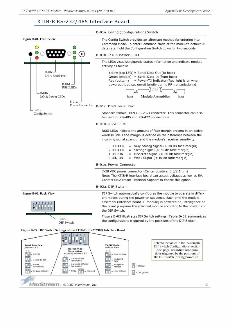
8/3/2019 Product Manual Xtend Oem Rfmodule
http://slidepdf.com/reader/full/product-manual-xtend-oem-rfmodule 60/71
9XTend™ OEM RF Module ‐ Product Manual v2.x4x [2007.01.04]
© 2007
MaxStream,
Inc.
60
Appendix B: Development Guide
XTIB-R RS-232/ 485 Interface Board
Figure B‐03. DIP Switch Settings of the XTIB‐R (RS‐232/485) Interface Board
B-01a. Config (Configuration) Switch
Figure B‐01. Front View The Config Switch provides an alternate method for entering into
Command Mode. To enter Command Mode at the module's default RF
data rate, hold the Configuration Switch down for two seconds.
B-01b. I/ O & P ower LEDs
The LEDs visualize gigantic status information and indicate module
activity as follows:
Yellow (top LED) = Serial Data Out (to host)
Green (middle) = Serial Data In (from host)
Red (bottom) = Power/TX Indicator (Red light is on when
powered; it pulses on/off briefly during RF transmission.))
B-01c. DB-9 Serial P ort
Standard female DB-9 (RS-232) connector. This connector can alsobe used for RS-485 and RS-422 connections.
B-01d. RSSI LEDs
RSSI LEDs indicate the amount of fade margin present in an active
wireless link. Fade margin is defined as the difference between the
incoming signal strength and the module's receiver sensitivity.
3 LEDs ON = Very Strong Signal (> 30 dB fade margin)
2 LEDs ON = Strong Signal (> 20 dB fade margin)
1 LED ON = Moderate Signal (> 10 dB fade margin)
0 LED ON = Weak Signal (< 10 dB fade margin)
B-01e. Pow er Connector
7-28 VDC power connector (Center positive, 5.5/2.1mm) Note: The XTIB-R interface board can accept voltages as low as 5V.
Contact MaxStream Technical Support to enable this option.
B-02a. DIP Switch
Figure B‐02. Back View DIP Switch automatically configures the module to operate in differ-
ent modes during the power-on sequence. Each time the module
assembly (interface board + module) is powered-on, intelligence on
the board programs the attached module according to the positions of
the DIP Switch.
Figure B-03 illustrates DIP Switch settings. Table B-02 summarizes
the configurations triggered by the positions of the DIP Switch.
B‐01a.
Config Switch
B‐01b.I/O & Power LEDs
B‐01c.DB‐9 Serial Port
B‐01dRSSI LEDs
B‐01e.Power Connector
B‐02a.
DIP Switch
Refer to the tables in the ‘Automatic DIP Switch Configurations’ section
[next page] regarding configura‐tions triggered by the positions of the DIP Switch (during power‐up).
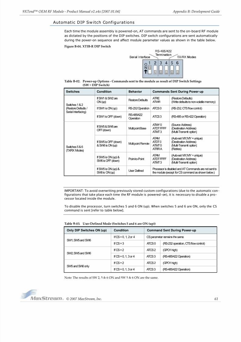
8/3/2019 Product Manual Xtend Oem Rfmodule
http://slidepdf.com/reader/full/product-manual-xtend-oem-rfmodule 61/71
9XTend™ OEM RF Module ‐ Product Manual v2.x4x [2007.01.04]
© 2007
MaxStream,
Inc.
61
Appendix B: Development Guide
Automatic DIP Sw itch Configurations
Each time the module assembly is powered-on, AT commands are sent to the on-board RF module
as dictated by the positions of the DIP switches. DIP switch configurations are sent automatically
during the power-on sequence and affect module parameter values as shown in the table below.
Figure B‐04. XTIB‐R DIP Switch
IMPORTANT: To avoid overwriting previously stored custom configurations (due to the automatic con-figurations that take place each time the RF module is powered-on), it is necessary to disable a pro-
cessor located inside the module.
To disable the processor, turn switches 5 and 6 ON (up). When switches 5 and 6 are ON, only the CS
command is sent [refer to table below].
Note: The results of SW 2, 5 & 6 ON and SW 5 & 6 ON are the same.
Table B‐02. Power‐up Options ‐ Commands sent to the module as result of DIP Switch Settings (SW = DIP Switch)
Switches Condition Behavior Commands Sent During Power-up
Switches 1 & 2 (Restore Defaults / Serial Interfacing)
If SW1 & SW2 areON (up)
Restore DefaultsATREATWR
(Restore Defaults)(Write defaults to non-volatile memory)
If SW1 is ON (up) RS-232 Operation ATCS 0 (RS-232, CTS flow control)
If SW1 is OFF (down)RS-485/422
Operation
ATCS 3 (RS-485 or RS-422 Operation)
Switches 5 & 6(TX/RX Modes)
If SW5 & SW6 areOFF (down)
Multipoint BaseATMY 0ATDT FFFFATMT 3
(Source Address)(Destination Address)(Multi-Transmit option)
If SW5 is OFF (down)& SW6 is ON (up)
Multipoint Remote
ATAMATDT 0ATMT 0ATRR A
(Auto-set MY, MY = unique)(Destination Address)(Multi-Transmit option)(Retries)
If SW5 is ON (up) &SW6 is OFF (down)
Point-to-PointATAMATDT FFFFATMT 3
(Auto-set MY, MY = unique)(Destination Address)(Multi-Transmit option)
If SW5 is ON (up) &SW6 is ON (up)
User DefinedProcessor is disabled and AT Commands are not sent tothe module (except for CS command as shown below.)
Table B‐03. User Defined Mode (Switches 5 and 6 are ON (up))
Only DIP Switches ON (up) Condition Command Sent During Power-up
SW1, SW5 and SW6
If CS = 0, 1, 2 or 4 CS parameter remains the same
If CS = 3 ATCS 0 (RS-232 operation, CTS flow control)
SW2, SW5 and SW6If CS = 2 ATCS 2 (GPO1 high)
If CS = 0, 1, 3 or 4 ATCS 3 (RS-485/422 Operation)
SW5 and SW6 onlyIf CS = 2 ATCS 2 (GPO1 high)
If CS = 0, 1, 3 or 4 ATCS 3 (RS-485/422 Operation)
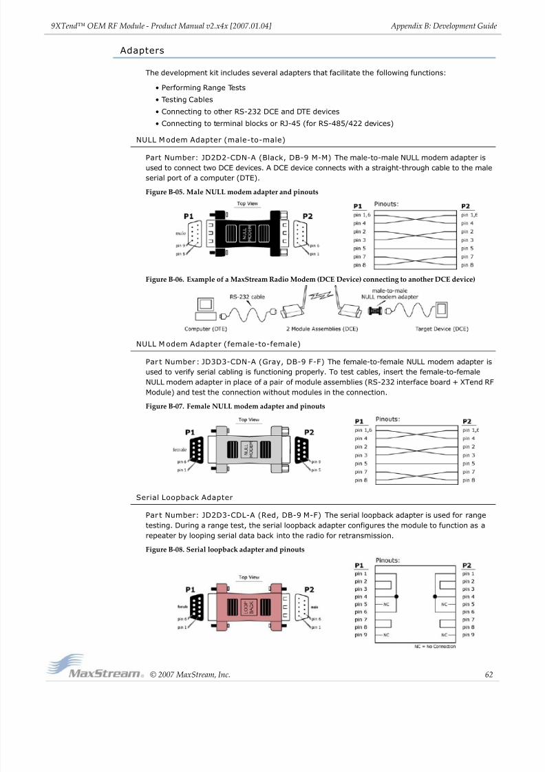
8/3/2019 Product Manual Xtend Oem Rfmodule
http://slidepdf.com/reader/full/product-manual-xtend-oem-rfmodule 62/71
9XTend™ OEM RF Module ‐ Product Manual v2.x4x [2007.01.04]
© 2007
MaxStream,
Inc.
62
Appendix B: Development Guide
Adapters
The development kit includes several adapters that facilitate the following functions:
• Performing Range Tests
• Testing Cables
• Connecting to other RS-232 DCE and DTE devices
• Connecting to terminal blocks or RJ-45 (for RS-485/422 devices)
NULL Modem Adapter (male-to-male)
Part Number: JD2D2-CDN-A (Black, DB-9 M-M) The male-to-male NULL modem adapter is
used to connect two DCE devices. A DCE device connects with a straight-through cable to the male
serial port of a computer (DTE).
Figure B‐05. Male NULL modem adapter and pinouts
Figure B‐06. Example of a MaxStream Radio Modem (DCE Device) connecting to another DCE device)
NULL M odem Adapter (female-to-female)
Par t Number: JD3D3-CDN-A (Gray, DB-9 F-F) The female-to-female NULL modem adapter is
used to verify serial cabling is functioning properly. To test cables, insert the female-to-female
NULL modem adapter in place of a pair of module assemblies (RS-232 interface board + XTend RF
Module) and test the connection without modules in the connection.
Figure B‐07. Female NULL modem adapter and pinouts
Serial Loopback Adapter
Par t Number: JD2D3-CDL-A (Red, DB-9 M-F) The serial loopback adapter is used for range
testing. During a range test, the serial loopback adapter configures the module to function as a
repeater by looping serial data back into the radio for retransmission.
Figure B‐08. Serial loopback adapter and pinouts

8/3/2019 Product Manual Xtend Oem Rfmodule
http://slidepdf.com/reader/full/product-manual-xtend-oem-rfmodule 63/71
9XTend™ OEM RF Module ‐ Product Manual v2.x4x [2007.01.04]
© 2007
MaxStream,
Inc.
63
Appendix B: Development Guide
Male DB-9 to RJ-45 Adapter
Part Number: JD2D2-CDN-A (Yellow ) This adapter facilitates adapting the DB-9 Connector of
the MaxStream Interface Board to a CAT5 cable (male DB9 to female RJ45).
Refer to the ‘RS-485 (4-wire) & RS-422 Operation’ sections for RS-485/422 connection guidelines.
Figure B‐09. Male DB‐9 to RJ‐45 Adapter and pinouts
Female DB-9 to RJ-45 Adapter
Part Number: JD3D3-CDN-A (Green) This adapter Facilitates adapting the DB-9 Connector of
the MaxStream Interface Board to a CAT5 cable (female DB9 to female RJ45).
Refer to the ‘RS-485 (4-wire) & RS-422 Operation’ sections for RS-485/422 connection guidelines.
Figure B‐10. Female DB‐9 to RJ‐45 Adapter and pinouts
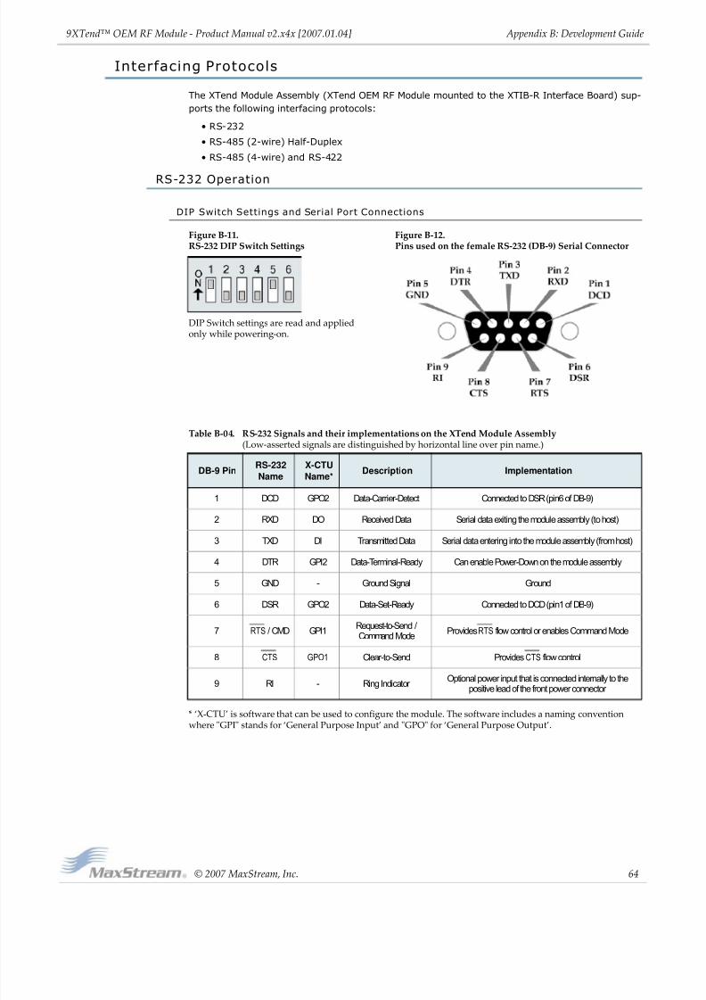
8/3/2019 Product Manual Xtend Oem Rfmodule
http://slidepdf.com/reader/full/product-manual-xtend-oem-rfmodule 64/71
9XTend™ OEM RF Module ‐ Product Manual v2.x4x [2007.01.04]
© 2007
MaxStream,
Inc.
64
Appendix B: Development Guide
Interfacing Protocols
The XTend Module Assembly (XTend OEM RF Module mounted to the XTIB-R Interface Board) sup-
ports the following interfacing protocols:
• RS-232
• RS-485 (2-wire) Half-Duplex
• RS-485 (4-wire) and RS-422
RS-232 Operation
DIP Switch Settings and Serial Port Connections
Figure B‐11. Figure B‐12. RS‐232 DIP Switch Settings Pins used on the female RS‐232 (DB‐9) Serial Connector
* ‘X‐CTU’ is software that can be used to configure the module. The software includes a naming convention
where ʺGPIʺ stands for ‘General Purpose Input’ and ʺGPOʺ for ‘General Purpose Output’.
Table B‐04. RS‐232 Signals and their implementations on the XTend Module Assembly
(Low‐asserted signals are distinguished by horizontal line over pin name.)
DB-9 PinRS-232
Name
X-CTU
Name*Description Implementation
1 DCD GPO2 Data-Carrier-Detect Connected to DSR (pin6 of DB-9)
2 RXD DO Received Data Serial data exiting the module assembly (to host)
3 TXD DI Transmitted Data Serial data entering into the module assembly (from host)
4 DTR GPI2 Data-Terminal-Ready Can enable Power-Down on the module assembly
5 GND - Ground Signal Ground
6 DSR GPO2 Data-Set-Ready Connected to DCD (pin1 of DB-9)
7 RTS / CMD GPI1Request-to-Send /Command Mode
ProvidesRTS flow control or enables Command Mode
8 CTS GPO1 Clear-to-Send Provides CTS flow control
9 RI - Ring Indicator Optional power input that is connected internally to the
positive lead of the front power connector
DIP Switch settings are read and applied
only while powering‐on.

8/3/2019 Product Manual Xtend Oem Rfmodule
http://slidepdf.com/reader/full/product-manual-xtend-oem-rfmodule 65/71
9XTend™ OEM RF Module ‐ Product Manual v2.x4x [2007.01.04]
© 2007
MaxStream,
Inc.
65
Appendix B: Development Guide
Wiring Diagrams
Figure B‐13. DTE Device (RS‐232, male DB‐9 connector) wired to a DCE Module Assembly (female DB‐9)
Figure B‐14. DCE Module Assembly (female DB‐9 connector) wired to a DCE Device (RS‐232, male DB‐9)
Sample Wi reless Connection : DTE <--> DCE DCE <--> DCE
Figure B‐15. Typical wireless link between DTE and DCE devices

8/3/2019 Product Manual Xtend Oem Rfmodule
http://slidepdf.com/reader/full/product-manual-xtend-oem-rfmodule 66/71
9XTend™ OEM RF Module ‐ Product Manual v2.x4x [2007.01.04]
© 2007
MaxStream,
Inc.
66
Appendix B: Development Guide
RS-485 (2-wire) Operation
When operating within the RS-485 protocols, all communications are half-duplex.
DIP Switch Settings and Serial Port Connections
Figure B‐16. Figure B‐17. RS‐485 (2‐wire) Half‐duplex Pins used on the female RS‐232 (DB‐9) DIP Switch Settings Serial Connector
Note: Refer to Figures B-09 and B-10 for RJ-45 connector pin designations used in
RS-485/422 environments.
Wiring Diagram
Figure B‐19. XTend Module Assembly in an RS‐485 (2‐wire) half‐duplex environment
Table B‐05. RS‐485 (2‐wire half‐duplex) signals and their implementations on the XTend Module Assembly
DB-9 Pin RS-485 Name Description Implementation
2 T/R- (TRA) Negative Data Line Transmit serial data to and from the XTend Module Assembly
5 GND Ground Signal Ground
8 T/R+ (TRB) Positive Data Line Transmit serial data to and from the XTend Module Assembly
9 PWR Power Optional power input that is connected internallyto the front power connector
1, 3, 4, 6, 7 not used
Figure B‐18. RS‐485 (2‐wire) w/ Termination (optional)
Termination is the 120 Ω resistor between T+ and T‐.
DIP Switch settings are read and applied only while powering‐on.
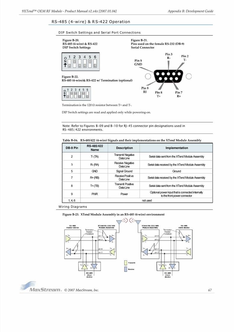
8/3/2019 Product Manual Xtend Oem Rfmodule
http://slidepdf.com/reader/full/product-manual-xtend-oem-rfmodule 67/71
9XTend™ OEM RF Module ‐ Product Manual v2.x4x [2007.01.04]
© 2007
MaxStream,
Inc.
67
Appendix B: Development Guide
RS-485 (4-wi re) & RS-422 Operation
DIP Switch Settings and Serial Port Connections
Figure B‐20. Figure B‐21. RS‐485 (4‐wire) & RS‐422 Pins used on the female RS‐232 (DB‐9) DIP Switch Settings Serial Connector
Note: Refer to Figures B-09 and B-10 for RJ-45 connector pin designations used inRS-485/422 environments.
Wiring Diagrams
Figure B‐23. XTend Module Assembly in an RS‐485 (4‐wire) environment
Table B‐06. RS‐485/422 (4‐wire) Signals and their implementations on the XTend Module Assembly
DB-9 PinRS-485/422
NameDescription Implementation
2 T- (TA)Transmit Negative
Data LineSerial data sent from the XTend Module Assembly
3 R- (RA)Receive Negative
Data LineSerial data received by the XTend Module Assembly
5 GND Signal Ground Ground
7 R+ (RB)Receive Positive
Data LineSerial data received by the XTend Module Assembly
8 T+ (TB)Transmit Positive
Data LineSerial data sent from the XTend Module Assembly
9 PWR Power Optional power input that is connected internally
to the front power connector
1, 4, 6 not used
Figure B‐22. RS‐485 (4‐wire)& RS‐422 w/ Termination (optional)
Termination is the 120 Ω resistor between T+ and T‐.
DIP Switch settings are read and applied only while powering‐on.

8/3/2019 Product Manual Xtend Oem Rfmodule
http://slidepdf.com/reader/full/product-manual-xtend-oem-rfmodule 68/71
9XTend™ OEM RF Module ‐ Product Manual v2.x4x [2007.01.04]
© 2007
MaxStream,
Inc.
68
Appendix B: Development Guide
Figure B‐24. XTend Module Assembly in an RS‐422 environment
RS-485/422 Connection Guidelines
The RS-485/422 protocol provides a solution for wired communications that can tolerate high
noise and push signals over long cable lengths. RS-485/422 signals can communicate as far as
4000 feet (1200 m). RS-232 signals are suitable for cable distances up to 100 feet (30.5 m).
RS-485 offers multi-drop capability in which up to 32 nodes can be connected. The RS-422 proto-
col is used for point-to-point communications.
Suggestions for integrating the XTend RF Module with the RS-485/ 422 protocol:
1. When using Ethernet twisted pair cabling: Select wires so that T+ and T- are connected to
each wire in a twisted pair. Likewise, select wires so that R+ and R- are connected to a
twisted pair. (For example, tie the green and white/green wires to T+ and T-.)
2. For straight-through Ethernet cable (not cross-over cable) - The following wiring pattern
works well: Pin3 to T+, Pin4 to R+, Pin5 to R-, Pin6 to T-
3. Note that the connecting cable only requires 4 wires (even though there are 8 wires).
4. When using phone cabling (RJ-11) - Pin2 in the cable maps to Pin3 on opposite end of
cable and Pin1 maps to Pin4 respectively.

8/3/2019 Product Manual Xtend Oem Rfmodule
http://slidepdf.com/reader/full/product-manual-xtend-oem-rfmodule 69/71
9XTend™ OEM RF Module ‐ Product Manual v2.x4x [2007.01.04]
© 2007
MaxStream,
Inc.
69
Appendix B: Development Guide
X-CTU Software
X-CTU is a MaxStream-provided software program used to interface with and configure Max-
Stream RF Modules. The software application is organized into the following four tabs:
• PC Settings tab - Setup PC serial ports for interfacing with an RF module
• Range Test tab - Test the RF module's range and monitor packets sent and received
• Terminal tab - Set and read RF module parameters using AT Commands
• Modem Configuration tab - Set and read RF module parametersFigure B‐11. X‐CTU User Interface (PC Settings, Range Test, Terminal and Modem Configuration tabs)
NOTE: PC Setting values are visible at the bottom of the Range Test, Terminal and Modem Configura-tion tabs. A shortcut for editing PC Setting values is available by clicking on any of the values.
Installation
Double-click the "setup_X-CTU.exe" file and follow prompts of the installation screens. This file is
located in the 'software' folder of the MaxStream CD and also under the 'Downloads' section of the
following web page: www.maxstream.net/support/downloads.php
Setup
Serial Communications Software
A terminal program is built into the X-CTU Software. Other terminal programs such as "HyperTer-
minal" can also be used to configure modules and monitor communications. When issuing AT Com-
mands through a terminal program interface, use the following syntax:
Figure B‐12. Syntax for sending AT Commands
NOTE: To read a parameter value stored in a register, leave the parameter field blank.
The example above issues the DT (Destination Address) command to change destination address
of the module to "0x1F". To save the new value to the module’s non-volatile memory, issue WR
(Write) command after modifying parameters.
To use the X-CTU software, a module assembly (An RF module mounted to an interface Board)
must be connected to a serial port of a PC.NOTE: Failure to enter AT Command Mode is most commonly due to baud rate mismatch. The
interface data rate and parity settings of the serial port ("PC Settings" tab) must match those of
the module (BD (Baud Rate) and NB (Parity) parameters respectively).
8/3/2019 Product Manual Xtend Oem Rfmodule
http://slidepdf.com/reader/full/product-manual-xtend-oem-rfmodule 70/71
© 2007
MaxStream,
Inc.
70
Appendix C: Additional Information
1-Year Warranty
XTend RF Modules from MaxStream, Inc. (the "Product") are warranted against defects in materi-
als and workmanship under normal use, for a period of 1-year from the date of purchase. In the
event of a product failure due to materials or workmanship, MaxStream will repair or replace the
defective product. For warranty service, return the defective product to MaxStream, shipping pre-
paid, for prompt repair or replacement.
The foregoing sets forth the full extent of MaxStream's warranties regarding the Product. Repair or
replacement at MaxStream's option is the exclusive remedy. THIS WARRANTY IS GIVEN IN LIEU
OF ALL OTHER WARRANTIES, EXPRESS OR IMPLIED, AND MAXSTREAM SPECIFICALLY DISCLAIMS
ALL WARRANTIES OF MERCHANTABILITY OR FITNESS FOR A PARTICULAR PURPOSE. IN NO EVENT
SHALL MAXSTREAM, ITS SUPPLIERS OR LICENSORS BE LIABLE FOR DAMAGES IN EXCESS OF THEPURCHASE PRICE OF THE PRODUCT, FOR ANY LOSS OF USE, LOSS OF TIME, INCONVENIENCE,
COMMERCIAL LOSS, LOST PROFITS OR SAVINGS, OR OTHER INCIDENTAL, SPECIAL OR CONSE-
QUENTIAL DAMAGES ARISING OUT OF THE USE OR INABILITY TO USE THE PRODUCT, TO THE
FULL EXTENT SUCH MAY BE DISCLAIMED BY LAW. SOME STATES DO NOT ALLOW THE EXCLUSION
OR LIMITATION OF INCIDENTAL OR CONSEQUENTIAL DAMAGES. THEREFORE, THE FOREGOING
EXCLUSIONS MAY NOT APPLY IN ALL CASES. This warranty provides specific legal rights. Other
rights which vary from state to state may also apply.
Ordering Information
Figure C‐01. Divisions of the XTend RF Module Part Numbers
For example:
XT09-SI = 9XTend OEM RF Module, 900 MHz, RPSMA Antenna, Industrial Temperature Rating

8/3/2019 Product Manual Xtend Oem Rfmodule
http://slidepdf.com/reader/full/product-manual-xtend-oem-rfmodule 71/71
9XTend™ OEM RF Module ‐ Product Manual v2.x4x [2007.01.04] Appendix C: Additional Information
Contact MaxStream
Free and unlimited technical support is included with every MaxStream Radio Modem sold. For the
best in wireless data solutions and support, please use the following resources:
MaxStream office hours are 8:00 am - 5:00 pm [U.S. Mountain Standard Time]
Documentation: www.maxstream.net/support/downloads.php
Technical Support: Phone. (866) 765-9885 toll-free U.S.A. & Canada
(801) 765-9885 Worldwide
Live Chat. www.maxstream.net
E-Mail. [email protected]
Related Documents