MC9S12D-FamilyPP Rev 6.1, 23-Oct-02 MC9S12D-Family Product Brief 16-Bit Microcontroller Designed for automotive multiplexing applications, members of the MC9S12D-Family of 16 bit Flash- based microcontrollers are fully pin compatible and enable users to choose between different memory and peripheral options for scalable designs. All MC9S12D-Family members are composed of standard on-chip peripherals including a 16-bit central processing unit (CPU12), up to 512K bytes of Flash EEPROM, 14K bytes of RAM, 4K bytes of EEPROM, two asynchronous serial communications interfaces (SCI), three serial peripheral interfaces (SPI), IIC-bus, an enhanced capture timer (ECT), two 8-channel 10-bit analog-to-digital converters (ADC), an eight-channel pulse-width modulator (PWM), J1850 interface and up to five CAN 2.0 A, B software compatible modules (MSCAN12). System resource mapping, clock generation, interrupt control and bus interfacing are managed by the system integration module (SIM). The MC9S12D-Family has full 16-bit data paths throughout, however, the external bus can operate in an 8-bit narrow mode so single 8-bit wide memory can be interfaced for lower cost systems. The inclusion of a PLL circuit allows power consumption and performance to be adjusted to suit operational requirements. In addition to the I/O ports available in each module, up to 22 I/O ports are available with interrupt capability allowing Wake-Up from STOP or WAIT mode. Features NOTE Not all features listed here are available in all configurations. Additional information about D and B family inter-operability is given in: EB386 “HCS12 D-Family Compatibility Considerations” and EB388 “Using the HCS12 D-Family as a development platform for the HCS12 B family” • 16-bit CPU12 — Upward compatible with M68HC11 instruction set — Interrupt stacking and programmer’s model identical to M68HC11 — HCS12 Instruction queue — Enhanced indexed addressing • Multiplexed bus — Single chip or expanded — 16 address/16 data wide or 16 address/8 data narrow modes — External address space 1MByte for Data and Program space (112 pin package only) • Wake-up interrupt inputs depending on the package option — 8-bit port H — 2-bit port J1:0 — 2-bit port J7:6 shared with IIC, CAN4 and CAN0 module — 8-bit port P shared with PWM or SPI1,2 • Memory options — 32K, 64K, 128K, 256K, 512K Byte Flash EEPROM — 1K, 2K, 4K Byte EEPROM — 2K, 4K, 8K, 12K, 14K Byte RAM Freescale Semiconductor, I Freescale Semiconductor, Inc. For More Information On This Produ Go to: www.freescale.com nc...

Welcome message from author
This document is posted to help you gain knowledge. Please leave a comment to let me know what you think about it! Share it to your friends and learn new things together.
Transcript
MC9S12D-FamilyPPRev 6.1, 23-Oct-02
MC9S12D-Family
Product Brief16-Bit Microcontroller
Designed for automotive multiplexing applications, members of the MC9S12D-Family of 16 bit Flash-based microcontrollers are fully pin compatible and enable users to choose between different memoryand peripheral options for scalable designs. All MC9S12D-Family members are composed of standardon-chip peripherals including a 16-bit central processing unit (CPU12), up to 512K bytes of FlashEEPROM, 14K bytes of RAM, 4K bytes of EEPROM, two asynchronous serial communicationsinterfaces (SCI), three serial peripheral interfaces (SPI), IIC-bus, an enhanced capture timer (ECT), two8-channel 10-bit analog-to-digital converters (ADC), an eight-channel pulse-width modulator (PWM),J1850 interface and up to five CAN 2.0 A, B software compatible modules (MSCAN12). Systemresource mapping, clock generation, interrupt control and bus interfacing are managed by the systemintegration module (SIM). The MC9S12D-Family has full 16-bit data paths throughout, however, theexternal bus can operate in an 8-bit narrow mode so single 8-bit wide memory can be interfaced forlower cost systems. The inclusion of a PLL circuit allows power consumption and performance to beadjusted to suit operational requirements. In addition to the I/O ports available in each module, up to 22I/O ports are available with interrupt capability allowing Wake-Up from STOP or WAIT mode.
Features
NOTENot all features listed here are available in all configurations.Additional information about D and B family inter-operability is given in:EB386 “HCS12 D-Family Compatibility Considerations” andEB388 “Using the HCS12 D-Family as a development platform for the HCS12 B family”
• 16-bit CPU12— Upward compatible with M68HC11 instruction set— Interrupt stacking and programmer’s model identical to M68HC11— HCS12 Instruction queue— Enhanced indexed addressing
• Multiplexed bus— Single chip or expanded— 16 address/16 data wide or 16 address/8 data narrow modes— External address space 1MByte for Data and Program space (112 pin package only)
• Wake-up interrupt inputs depending on the package option— 8-bit port H— 2-bit port J1:0— 2-bit port J7:6 shared with IIC, CAN4 and CAN0 module— 8-bit port P shared with PWM or SPI1,2
• Memory options— 32K, 64K, 128K, 256K, 512K Byte Flash EEPROM— 1K, 2K, 4K Byte EEPROM— 2K, 4K, 8K, 12K, 14K Byte RAM
Fre
esc
ale
Se
mic
on
du
cto
r, I
Freescale Semiconductor, Inc.
For More Information On This Produ Go to: www.freescale.com
nc
...
RXZB30
logo

MC9S2 PRODUCT PROPOSAL, Rev 6.1, 23-Oct-02
• Analog-to-Digital Converters— One or two 8-channel modules with 10-bit resolution depending on the package option— External conversion trigger capability
• Up to five 1M bit per second, CAN 2.0 A, B software compatible modules— Five receive and three transmit buffers— Flexible identifier filter programmable as 2 x 32 bit, 4 x 16 bit or 8 x 8 bit— Four separate interrupt channels for Receive, Transmit, Error and Wake-up— Low-pass filter wake-up function in STOP mode— Loop-back for self test operation
• Enhanced Capture Timer (ECT)— 16-bit main counter with 7-bit prescaler— 8 programmable input capture or output compare channels; 4 of the 8 input captures with buffer— Input capture filters and buffers, three successive captures on four channels, or two captures on four
channels with a capture/compare selectable on the remaining four— Four 8-bit or two 16-bit pulse accumulators— 16-bit modulus down-counter with 4-bit prescaler— Four user-selectable delay counters for signal filtering
• 8 PWM channels with programmable period and duty cycle (7 channels on 80 Pin Packages)— 8-bit, 8-channel or 16-bit, 4-channel— Separate control for each pulse width and duty cycle— Center- or left-aligned outputs— Programmable clock select logic with a wide range of frequencies
• Serial interfaces— Two asynchronous serial communications interfaces (SCI)— Up to three synchronous serial peripheral interfaces (SPI)— IIC
• SAE J1850 Compatible Module (BDLC)— 10.4 kbps Variable Pulse Width format— Byte level receive and transmit— 4x receive mode supported
• SIM (System Integration Module)— CRG (windowed COP watchdog, real time interrupt, clock monitor, clock generation and reset)— MEBI (multiplexed external bus interface)— INT (interrupt control)
• Clock generation— Phase-locked loop clock frequency multiplier— Limp home mode in absence of external clock— Clock Monitor— Low power 0.5 to 16 MHz crystal oscillator reference clock
• Operating frequency for ambient temperatures TA -40°C <= TA <= 125°C— 50MHz equivalent to 25MHz Bus Speed for single chip
40MHz equivalent to 20MHz Bus Speed in expanded bus modes.
• Internal 5V to 2.5V Regulator
• 112-Pin LQFP or 80-Pin QFP package— I/O lines with 5V input and drive capability— 5V A/D converter inputs and 5V I/O— 2.5V logic supply
• Development support— Single-wire background debug™ mode (BDM)— On-chip hardware breakpoints
Fre
esc
ale
Se
mic
on
du
cto
r, I
Freescale Semiconductor, Inc.
For More Information On This Product, Go to: www.freescale.com
nc
...

PRODUCT PROPOSAL, Rev 6.1, 23-Oct-02 3
• Pin out explanations:— A/D is the number of modules/total number of A/D channels. — I/O is the sum of ports capable to act as digital input or output.
112 Pin Packages: Port A = 8, B = 8, E = 6 + 2 input only, H = 8, J = 4, K = 7, M = 8, P = 8, S = 8, T = 8, PAD = 16 inputonly.22 inputs provide Interrupt capability (H =8, P= 8, J = 4, IRQ, XIRQ)
80 Pin Packages:Port A = 8, B = 8, E = 6 + 2 input only, J = 2, M = 6, P = 7, S = 4, T = 8, PAD = 8 input only.11 inputs provide Interrupt capability (P= 7, J = 2, IRQ, XIRQ)
— CAN0 pins are shared between J1850 pins.— CAN0 can be routed under software control from PM1:0 to pins PM3:2 or PM5:4 or PJ7:6.— CAN4 pins are shared between IIC pins.— CAN4 can be routed under software control from PJ7:6 to pins PM5:4 or PM7:6.— Versions with 4 CAN modules will have CAN0, CAN1, CAN2 and CAN4.— Versions with 3 CANs modules will have CAN0, CAN1 and CAN4.— Versions with 2 CAN modules will have CAN0 and CAN4.— Versions with one CAN module will have CAN0.— Versions with 2 SPI modules will have SPI0 and SPI1.— Versions with 1 SPI will have SPI0.— SPI0 can be routed to either Ports PS7:4 or PM5:2.— SPI2 pins are shared with PWM7:4; In 112 pin versions SPI2 can be routed under software control to
PH7:4. In 80 pin packages SS-signal of SPI2 is not bonded out!
NOTECAN and SPI routing features are not available on the 1st PC9S12DP256 mask set 0K36N!
Table 1 List of MC9S12D-Family members
Flash RAM EEPROM Package Device CAN J1850 SCI SPI IIC A/D PWM I/O
512K 14K 4K 112LQFP
DP512 5 1 2 3 1 2/16 8 91
DT512 3 0 2 3 1 2/16 8 91
DJ512 2 1 2 3 1 2/16 8 91
256K 12K 4K
112LQFP
DT256 3 0 2 3 1 2/16 8 91
DJ256 2 1 2 3 1 2/16 8 91
DG256 2 0 2 3 1 2/16 8 91
80QFPDJ256 2 1 2 3 1 1/8 7 59
DG256 2 0 2 3 1 1/8 7 59
128K 8K 2K
112LQFP
DT128 3 0 2 2 1 2/16 8 91
DJ128 2 1 2 2 1 2/16 8 91
DG128 2 0 2 2 1 2/16 8 91
80QFPDJ128 2 1 2 2 1 1/8 7 59
DG128 2 0 2 2 1 1/8 7 59
64K 4K 1K
112LQFPDJ64 1 1 2 1 1 2/16 8 91
D64 1 0 2 1 1 2/16 8 91
80QFPDJ64 1 1 2 1 1 1/8 7 59
D64 1 0 2 1 1 1/8 7 59
32K 2K 1K 80QFP D32 1 0 2 1 0 1/8 7 59
Fre
esc
ale
Se
mic
on
du
cto
r, I
Freescale Semiconductor, Inc.
For More Information On This Product, Go to: www.freescale.com
nc
...

MC9S4 PRODUCT PROPOSAL, Rev 6.1, 23-Oct-02
32K - 512K Byte Flash EEPROM
2K - 14K Byte RAM
Enhanced Capture
RESET
EXTALXTAL
VDD1,2VSS1,2
SCI0
1K - 4K Byte EEPROM
BKGD
R/W
MODB
XIRQ
NOACC/XCLKS
SystemIntegration
Module(SIM)
VDDR
CPU12
Periodic InterruptCOP WatchdogClock Monitor
Single-wire Background
Breakpoints
PLLVSSPLL
XFCVDDPLL
Multiplexed Address/Data Bus
VDDAVSSA
VRHVRLATD0
MultiplexedWide Bus
Multiplexed
VDDXVSSX
Internal Logic 2.5V
Narrow Bus
PPAGE
VDDPLL VSSPLL
PLL 2.5V
IRQ
LSTRBECLKMODA
PA
4P
A3
PA
2P
A1
PA
0
PA
7P
A6
PA
5
TEST
AD
DR
12A
DD
R11
AD
DR
10A
DD
R9
AD
DR
8
AD
DR
15A
DD
R14
AD
DR
13D
ATA
12D
ATA
11D
ATA
10D
ATA
9D
ATA
8
DA
TA15
DA
TA14
DA
TA13
PB
4P
B3
PB
2P
B1
PB
0
PB
7P
B6
PB
5A
DD
R4
AD
DR
3A
DD
R2
AD
DR
1A
DD
R0
AD
DR
7A
DD
R6
AD
DR
5D
ATA
4D
ATA
3D
ATA
2D
ATA
1D
ATA
0
DA
TA7
DA
TA6
DA
TA5
DA
TA4
DA
TA3
DA
TA2
DA
TA1
DA
TA0
DA
TA7
DA
TA6
DA
TA5
PE3PE4PE5PE6PE7
PE0PE1PE2
AN2
AN6
AN0
AN7
AN1
AN3AN4AN5
PAD03PAD04PAD05PAD06PAD07
PAD00PAD01PAD02
IOC2
IOC6
IOC0
IOC7
IOC1
IOC3IOC4IOC5
PT3PT4PT5PT6PT7
PT0PT1PT2
VRHVRL
VDDAVSSA
VRHVRLATD1
AN2
AN6
AN0
AN7
AN1
AN3AN4AN5
PAD11PAD12PAD13PAD14PAD15
PAD08PAD09PAD10
VDDAVSSA
RXDTXD
MISOMOSI
PS3PS4PS5
PS0PS1PS2SCI1
RXDTXD
PP3PP4PP5PP6PP7
PP0PP1PP2
PIX2
PIX0PIX1
PIX3
ECS
PK3
PK7
PK0PK1
XADDR17
ECS/ROMONE
XADDR14XADDR15XADDR16
SCKSS
PS6PS7
SPI0
IIC SDASCL
PJ6PJ7
CAN0RXCANTXCAN
PM1PM0
CAN1RXCANTXCAN
PM2PM3
CAN2RXCANTXCAN
PM4PM5
CAN3RXCANTXCAN
PM6PM7
KWH2
KWH6
KWH0
KWH7
KWH1
KWH3KWH4KWH5
PH3PH4PH5PH6PH7
PH0PH1PH2
KWJ0KWJ1
PJ0PJ1
I/O Driver 5V
VDDAVSSA
A/D Converter 5V &
DDRA DDRB
PTA PTB
DD
RE
PT
E
AD
1
AD
0
PT
K
DD
RK
PT
T
DD
RT
PT
P
DD
RP
PT
S
DD
RS
PT
M
DD
RM
PT
H
DD
RH
PT
J
DD
RJ
PK2
BDLC RXBTXB
Clock andResetGenerationModule
Voltage RegulatorVSSR
Debug Module
VDD1,2VSS1,2
VREGEN
VDDRVSSR
Voltage Regulator 5V & I/O
Not all functionality shown in thisBlock diagram is available in all Versions!
CAN4RXCANTXCAN
MISOMOSISCK
SS
SPI2
MISOMOSISCK
SS
SPI1
PIX4PIX5
PK4PK5
XADDR18XADDR19
Voltage Regulator Reference
KWP2
KWP6
KWP0
KWP7
KWP1
KWP3KWP4KWP5
KWJ6KWJ7
Timer
(J1850)
Sign
als
show
n in
Bol
d ar
e no
t ava
ilabl
e on
the
80 P
in P
acka
ge
Mod
ule
to P
ort R
outin
g
PWM2
PWM6
PWM0
PWM7
PWM1
PWM3PWM4PWM5
PWM
Fre
esc
ale
Se
mic
on
du
cto
r, I
Freescale Semiconductor, Inc.
For More Information On This Product, Go to: www.freescale.com
nc
...

PRODUCT PROPOSAL, Rev 6.1, 23-Oct-02 5
Figure 1 Pin assignments 112 LQFP for MC9S12D-Family
VRHVDDAPAD15/AN15/ETRIG1PAD07/AN07/ETRIG0PAD14/AN14PAD06/AN06PAD13/AN13PAD05/AN05PAD12/AN12PAD04/AN04PAD11/AN11PAD03/AN03PAD10/AN10PAD02/AN02PAD09/AN09PAD01/AN01PAD08/AN08PAD00/AN00VSS2VDD2PA7/ADDR15/DATA15PA6/ADDR14/DATA14PA5/ADDR13/DATA13PA4/ADDR12/DATA12PA3/ADDR11/DATA11PA2/ADDR10/DATA10PA1/ADDR9/DATA9PA0/ADDR8/DATA8
PP4/
KWP4
/PW
M4/
MIS
O2
PP5/
KPW
5/PW
M5/
MO
SI2
PP6/
KW
P6/P
WM
6/SS
2PP
7/KW
P7/P
WM
7/SC
K2PK
7/EC
S /RO
MO
NEVD
DX
VSSX
PM0/
RXC
AN0/
RXB
PM1/
TXC
AN0/
TXB
PM2/
RXC
AN1/
RXC
AN0/
MIS
O0
PM3/
TXC
AN1/
TXC
AN0/
SS0
PM4/
RXC
AN2/
RXC
AN0/
RXC
AN4/
MO
SI0
PM5/
TXC
AN2/
TXC
AN0/
TXC
AN4/
SCK0
PJ6/
KWJ6
/RXC
AN4/
SDA/
RXC
AN0
PJ7/
KWJ7
/TXC
AN4/
SCL/
TXC
AN0
VREG
ENPS
7/SS
0PS
6/SC
K0
PS5/
MO
SI0
PS4/
MIS
O0
PS3/
TXD
1PS
2/R
XD1
PS1/
TXD
0PS
0/R
XD0
PM6/
RXC
AN3/
RXC
AN4
PM7/
TXC
AN3/
TXCA
N4VS
SAVR
L
SS1/PWM3/KWP3/PP3SCK1/PWM2/KWP2/PP2
MOSI1/PWM1/KWP1/PP1MISO1/PWM0/KWP0/PP0
XADDR17/PK3XADDR16/PK2XADDR15/PK1XADDR14/PK0
IOC0/PT0IOC1/PT1IOC2/PT2IOC3/PT3
VDD1VSS1
IOC4/PT4IOC5/PT5IOC6/PT6IOC7/PT7
XADDR19/PK5XADDR18/PK4
KWJ1/PJ1KWJ0/PJ0
MODC/TAGHI/BKGDADDR0/DATA0/PB0ADDR1/DATA1/PB1ADDR2/DATA2/PB2ADDR3/DATA3/PB3ADDR4/DATA4/PB4
ADD
R5/
DAT
A5/P
B5AD
DR
6/D
ATA6
/PB6
ADD
R7/
DAT
A7/P
B7SS
2 /KW
H7/P
H7
SCK2
/KW
H6/P
H6
MO
SI2/
KWH5
/PH
5M
ISO
2/KW
H4/P
H4
XCLK
S /N
OAC
C/P
E7M
OD
B/IP
IPE1
/PE6
MO
DA/
IPIP
E0/P
E5EC
LK/P
E4VS
SRVD
DR
RES
ETVD
DPL
LXF
CVS
SPLL
EXTA
LXT
ALTE
STSS
1 /KW
H3/P
H3
SCK1
/KW
H2/P
H2
MO
SI1/
KWH1
/PH
1M
ISO
1/KW
H0/P
H0
LSTR
B /TA
GLO
/PE3
R/W
/PE2
IRQ
/PE1
XIR
Q/P
E0
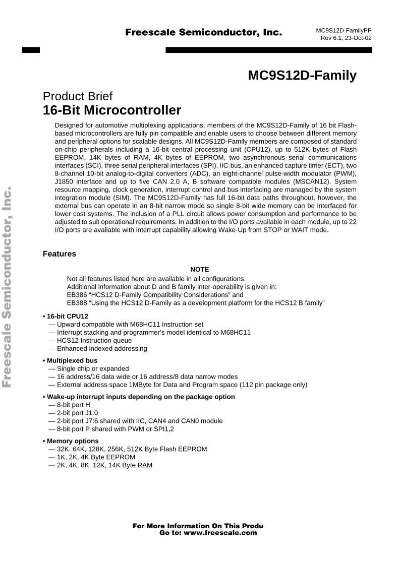
Signals shown in Bold are not available on the 80 Pin Package
MC9S12D-Family112LQFP
112
111
110
109
108
107
106
105
104
103
102
101
100 99 98 97 96 95 94 93 92 91 90 89 88 87 86 85
12345678910111213141516171819202122232425262728
29 30 31 32 33 34 35 36 37 38 39 40 41 42 43 44 45 46 47 48 49 50 51 52 53 54 55 56
84838281807978777675747372717069686766656463626160595857
Fre
esc
ale
Se
mic
on
du
cto
r, I
Freescale Semiconductor, Inc.
For More Information On This Product, Go to: www.freescale.com
nc
...
MC9S6 PRODUCT PROPOSAL, Rev 6.1, 23-Oct-02
Figure 2 Pin Assignments in 80 QFP for MC9S12D-Family
1234567891011121314151617181920
80 79 78 77 76 75 74 73 72 71 70 69 68 67 66 65 64 63 62 61
21 22 23 24 25 26 27 28 29 30 31 32 33 34 35 36 37 38 39 40MC9S12D-Family
80 QFP
VRHVDDAPAD07/AN07/ETRIG0PAD06/AN06PAD05/AN05PAD04/AN04PAD03/AN03PAD02/AN02PAD01/AN01PAD00/AN00VSS2VDD2PA7/ADDR15/DATA15PA6/ADDR14/DATA14PA5/ADDR13/DATA13PA4/ADDR12/DATA12PA3/ADDR11/DATA11PA2/ADDR10/DATA10PA1/ADDR9/DATA9PA0/ADDR8/DATA8
PP4/
KWP4
/PW
M4/
MIS
O2
PP5/
KWP5
/PW
M5/
MO
SI2
PP7/
KWP7
/PW
M7/
SCK2
VDD
XVS
SXPM
0/R
XCAN
0/R
XBPM
1/TX
CAN
0/TX
BPM
2/R
XCAN
1/R
XCAN
0/M
ISO
0PM
3/TX
CAN
1/TX
CAN
0/SS
0PM
4/R
XCAN
2/R
XCAN
0/R
XCAN
4/M
OSI
0PM
5/TX
CAN
2/TX
CAN
0/TX
CAN
4/SC
K0PJ
6/KW
J6/R
XCAN
4/SD
A/R
XCAN
0PJ
7/KW
J7/T
XCAN
4/SC
L/TX
CAN
0VR
EGEN
PS3/
TXD
1PS
2/R
XD1
PS1/
TXD
0PS
0/R
XD0
VSSA
VRL
SS1/PWM3/KWP3/PP3SCK1/PWM2/KWP2/PP2
MOSI1/PWM1/KWP1/PP1MISO1/PWM0/KWP0/PP0
IOC0/PT0IOC1/PT1IOC2/PT2IOC3/PT3
VDD1VSS1
IOC4/PT4IOC5/PT5IOC6/PT6IOC7/PT7
MODC/TAGHI/BKGDADDR0/DATA0/PB0ADDR1/DATA1/PB1ADDR2/DATA2/PB2ADDR3/DATA3/PB3ADDR4/DATA4/PB4
ADD
R5/
DAT
A5/P
B5AD
DR
6/D
ATA6
/PB6
ADD
R7/
DAT
A7/P
B7XC
LKS /
NO
ACC
/PE7
MO
DB/
IPIP
E1/P
E6M
OD
A/IP
IPE0
/PE5
ECLK
/PE4
VSSR
VDD
RR
ESET
VDD
PLL
XFC
VSSP
LLEX
TAL
XTAL
TEST
LSTR
B /TA
GLO
/PE3
R/W
/PE2
IRQ
/PE1
XIR
Q/P
E0
6059585756555453525150494847464544434241
Fre
esc
ale
Se
mic
on
du
cto
r, I
Freescale Semiconductor, Inc.
For More Information On This Product, Go to: www.freescale.com
nc
...

PRODUCT PROPOSAL, Rev 6.1, 23-Oct-02 7
Figure 3 MC9S12Dx512 User Configurable Memory Map
$0000
$FFFF
$C000
$8000
$4000
$0400$0800
$FF00
EXT
NORMALSINGLE CHIP
EXPANDED SPECIALSINGLE CHIP
VECTORSVECTORS VECTORS
$FF00
$FFFF
BDM(If Active)
$C000
$FFFF
16K Fixed Flash EEPROM
2K, 4K, 8K or 16K Protected Boot Sector
$8000
$BFFF
16K Page Windowthirty two * 16K Flash EEPROM Pages
$4000
$6FFF
12K Fixed Flash EEPROM
0.5K, 1K, 2K or 4K Protected Sector
$0800
$3FFF
$7000
$7FFF
4K Bytes EEPROM
Mappable to any 4K Boundary
$0000
$03FF
1K Register Space
Mappable to any 2K Boundary
Mappable to any 16K Boundary
14K Bytes RAM
4K Flash overlapped by EEPROM in this configuration
Alignable to top ($0800 - $3FFF)or bottom ($0000 - $37FF)
The figure shows a useful map, which is not the map out of reset. After reset the map is:$0000 - $03FF: Register Space$0800 - $3FFF: 14K RAM$0000 - $0FFF: 4K EEPROM (1k $0400 - $07FF visible, $0000 - $03FF and $0800 - $0FFF are not visible)Various possibilities to make more of the EEPROM fully visible are available, one of them is shown above
EXT
$7000
Fre
esc
ale
Se
mic
on
du
cto
r, I
Freescale Semiconductor, Inc.
For More Information On This Product, Go to: www.freescale.com
nc
...

MC9S8 PRODUCT PROPOSAL, Rev 6.1, 23-Oct-02
Figure 4 MC9S12Dx256 User Configurable Memory Map
$0000
$FFFF
$C000
$8000
$4000
$0400
$1000
$FF00
EXT
NORMALSINGLE CHIP
EXPANDED SPECIALSINGLE CHIP
VECTORSVECTORS VECTORS
$FF00
$FFFF
BDM(If Active)
$C000
$FFFF
16K Fixed Flash EEPROM
2K, 4K, 8K or 16K Protected Boot Sector
$8000
$BFFF
16K Page Windowsixteen * 16K Flash EEPROM Pages
$4000
$7FFF16K Fixed Flash EEPROM
0.5K, 1K, 2K or 4K Protected Sector
$1000
$3FFF
$0000
$0FFF
4K Bytes EEPROM
Mappable to any 4K Boundary
$0000
$03FF
1K Register Space
Mappable to any 2K Boundary
Mappable to any 16K Boundary
12K Bytes RAM
Initially overlapped by register space
Alignable to top ($1000 - $3FFF)or bottom ($0000 - $2FFF)
Fre
esc
ale
Se
mic
on
du
cto
r, I
Freescale Semiconductor, Inc.
For More Information On This Product, Go to: www.freescale.com
nc
...

PRODUCT PROPOSAL, Rev 6.1, 23-Oct-02 9
Figure 5 MC9S12Dx128 User Configurable Memory Map
$0000
$FFFF
$C000
$8000
$4000
$0400$0800$1000$2000
$FF00
EXT
NORMALSINGLE CHIP
EXPANDED SPECIALSINGLE CHIP
VECTORSVECTORS VECTORS
$FF00
$FFFF
BDM(If Active)
$C000
$FFFF
16K Fixed Flash EEPROM
2K, 4K, 8K or 16K Protected Boot Sector
$8000
$BFFF
16K Page Windoweight * 16K Flash EEPROM Pages
$4000
$7FFF16K Fixed Flash EEPROM
0.5K, 1K, 2K or 4K Protected Sector
$2000
$3FFF
8K Bytes RAM
Mappable to any 8K Boundary
$0800
$0FFF
2K Bytes EEPROM
Mappable to any 2K Boundary
$0000
$03FF
1K Register Space
Mappable to any 2K Boundary
The figure shows a useful map, which is not the map out of reset. After reset the map is:$0000 - $03FF: Register Space$0000 - $1FFF: 8K RAM$0000 - $07FF: 1K EEPROM (not visible)
Fre
esc
ale
Se
mic
on
du
cto
r, I
Freescale Semiconductor, Inc.
For More Information On This Product, Go to: www.freescale.com
nc
...

MC9S10 PRODUCT PROPOSAL, Rev 6.1, 23-Oct-02
Figure 6 MC9S12Dx64 User Configurable Memory Map
$0000
$FFFF
$C000
$8000
$4000
$0400$0800
$1000
$3000
$FF00
EXT
NORMALSINGLE CHIP
EXPANDED SPECIALSINGLE CHIP
VECTORSVECTORS VECTORS
$FF00
$FFFF
BDM(If Active)
$C000
$FFFF
16K Fixed Flash EEPROM
2K, 4K, 8K or 16K Protected Boot Sector
$8000
$BFFF
16K Page Windowfour * 16K Flash EEPROM Pages
$4000
$7FFF16K Fixed Flash EEPROM
0.5K, 1K, 2K or 4K Protected Sector
$3000
$3FFF
4K Bytes RAM
Mappable to any 4K Boundary
$0800
$0FFF
1K Bytes EEPROM
Mappable to any 2K Boundary
$0000
$03FF
1K Register Space
Mappable to any 2K Boundary
repeated twice in the 2K space
The figure shows a useful map, which is not the map out of reset. After reset the map is:$0000 - $03FF: Register Space$0000 - $0FFF: 4K RAM$0000 - $07FF: 1K EEPROM (not visible)
Fre
esc
ale
Se
mic
on
du
cto
r, I
Freescale Semiconductor, Inc.
For More Information On This Product, Go to: www.freescale.com
nc
...

PRODUCT PROPOSAL, Rev 6.1, 23-Oct-02 11
Figure 7 MC9S12Dx32 User Configurable Memory Map
$0000
$FFFF
$C000
$8000
$0400$0800
$1000
$4000
$FF00
EXT
NORMALSINGLE CHIP
EXPANDED SPECIALSINGLE CHIP
VECTORSVECTORS VECTORS
$FF00
$FFFF
BDM(If Active)
$C000
$FFFF
16K Fixed Flash EEPROM
2K, 4K, 8K or 16K Protected Boot Sector
$8000
$BFFF
16K Fixed Flash EEPROM
two * 16K Flash EEPROM Pages0.5K, 1K, 2K or 4K Protected Sector
$3800
$3FFF
2K Bytes RAM
Mappable to any 2K Boundary
$0800
$0FFF
1K Bytes EEPROM
Mappable to any 2K Boundary
$0000
$03FF
1K Register Space
Mappable to any 2K Boundary
$3800
Repeated twice in the 2K space
The figure shows a useful map, which is not the map out of reset. After reset the map is:$0000 - $03FF: Register Space$0800 - $0FFF: 2K RAM$0000 - $07FF: 1K EEPROM (not visible)
Fre
esc
ale
Se
mic
on
du
cto
r, I
Freescale Semiconductor, Inc.
For More Information On This Product, Go to: www.freescale.com
nc
...
MC9S12 PRODUCT PROPOSAL, Rev 6.1, 23-Oct-02
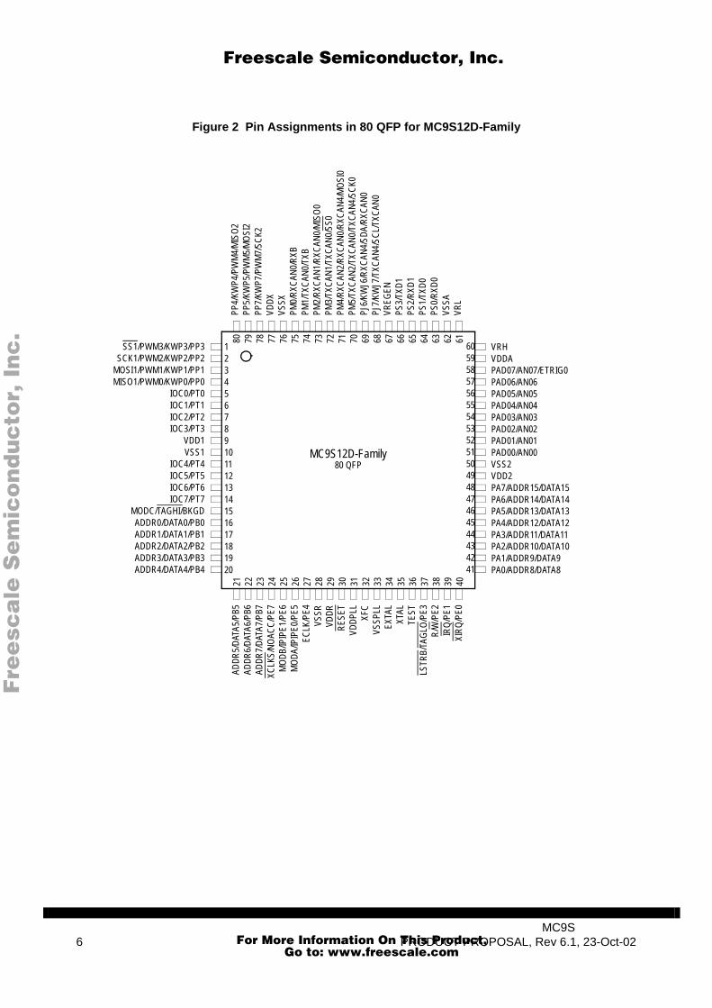
Figure 8 112-pin LQFP Mechanical Dimensions (case no. 987)
DIMA
MIN MAX20.000 BSC
MILLIMETERS
A1 10.000 BSCB 20.000 BSC
B1 10.000 BSCC --- 1.600
C1 0.050 0.150C2 1.350 1.450D 0.270 0.370E 0.450 0.750F 0.270 0.330G 0.650 BSCJ 0.090 0.170K 0.500 REFP 0.325 BSCR1 0.100 0.200R2 0.100 0.200S 22.000 BSC
S1 11.000 BSCV 22.000 BSC
V1 11.000 BSCY 0.250 REFZ 1.000 REF
AA 0.090 0.160θ
θθθ 11 °
11 °13 °
7 °
13 °
VIEW Y
L-M0.20 NT4X 4X 28 TIPS
PIN 1IDENT
1
112 85
84
28 57
29 56
B V
V1B1
A1
S1
A
S
VIEW AB
0.10
3
CC2
θ
2θ0.050
SEATINGPLANE
GAGE PLANE
1θ
θ
VIEW AB
C1
(Z)
(Y)E
(K)
R2
R1 0.25
J1
VIEW Y
J1
P
G108X
4X
SECTION J1-J1
BASE
ROTATED 90 COUNTERCLOCKWISE°
METAL
J AA
FD
L-MM0.13 NT
123
CL
L-M0.20 NT
L
N
M
T
T
112X
XX=L, M OR N
R
R
NOTES:1. DIMENSIONING AND TOLERANCING PER
ASME Y14.5M, 1994.2. DIMENSIONS IN MILLIMETERS.3. DATUMS L, M AND N TO BE DETERMINED AT
SEATING PLANE, DATUM T.4. DIMENSIONS S AND V TO BE DETERMINED AT
SEATING PLANE, DATUM T.5. DIMENSIONS A AND B DO NOT INCLUDE
MOLD PROTRUSION. ALLOWABLE PROTRUSION IS 0.25 PER SIDE. DIMENSIONS A AND B INCLUDE MOLD MISMATCH.
6. DIMENSION D DOES NOT INCLUDE DAMBAR
8 ° 3 ° 0 °
Fre
esc
ale
Se
mic
on
du
cto
r, I
Freescale Semiconductor, Inc.
For More Information On This Product, Go to: www.freescale.com
nc
...
PRODUCT PROPOSAL, Rev 6.1, 23-Oct-02 13
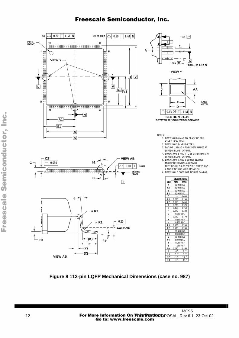
Figure 9 80-pin QFP Mechanical Dimensions (case no. 841B)
NOTES:1. DIMENSIONING AND TOLERANCING PER
ANSI Y14.5M, 1982.2. CONTROLLING DIMENSION: MILLIMETER.3. DATUM PLANE -H- IS LOCATED AT BOTTOM OF
LEAD AND IS COINCIDENT WITH THE LEAD WHERE THE LEAD EXITS THE PLASTIC BODY AT THE BOTTOM OF THE PARTING LINE.
4. DATUMS -A-, -B- AND -D- TO BE DETERMINED AT DATUM PLANE -H-.
5. DIMENSIONS S AND V TO BE DETERMINED AT SEATING PLANE -C-.
6. DIMENSIONS A AND B DO NOT INCLUDE MOLD PROTRUSION. ALLOWABLE PROTRUSION IS 0.25 PER SIDE. DIMENSIONS A AND B DO INCLUDE MOLD MISMATCHAND ARE DETERMINED AT DATUM PLANE -H-.
7. DIMENSION D DOES NOT INCLUDE DAMBARPROTRUSION. ALLOWABLE DAMBARPROTRUSION SHALL BE 0.08 TOTAL IN EXCESS OF THE D DIMENSION AT MAXIMUM MATERIAL CONDITION. DAMBAR CANNOTBE LOCATED ON THE LOWER RADIUS ORTHE FOOT.
SECTION B-B
61
60
DETAIL A
L
41
40
80
-A-
L
-D-A
SA-BM0.20 D SH
0.05 A-B
S
1 20
21
-B-
B V
J
F
N
D
VIEW ROTATED 90°
DETAIL A
B
BP
-A-,-B-,-D-
E
H
GM
MDETAIL C
SEATINGPLANE
-C-
C DATUMPLANE
0.10
-H-
DATUMPLANE -H-
U
T
R
QKW
XDETAIL C
DIM MIN MAXMILLIMETERS
A 13.90 14.10B 13.90 14.10C 2.15 2.45D 0.22 0.38E 2.00 2.40F 0.22 0.33G 0.65 BSCH --- 0.25J 0.13 0.23K 0.65 0.95L 12.35 REFM 5 10 N 0.13 0.17P 0.325 BSCQ 0 7 R 0.13 0.30S 16.95 17.45T 0.13 ---U 0 ---V 16.95 17.45W 0.35 0.45X 1.6 REF
° °
° °
°
SA-BM0.20 D SCS
A-B
M0.
20D
SH
0.05
D
SA-
BM
0.20
DS
CSA-BM0.20 D SC
Fre
esc
ale
Se
mic
on
du
cto
r, I
Freescale Semiconductor, Inc.
For More Information On This Product, Go to: www.freescale.com
nc
...
Fre
esc
ale
Se
mic
on
du
cto
r, I
Freescale Semiconductor, Inc.
More Information On This Product, Go to: www.freescale.com
nc
...
RXZB30
hibbertleft
RXZB30
disclaimer
RXZB30
rohstext
RXZB30
logo
Related Documents