IEEE TRANSACTIONS ON NANOTECHNOLOGY, VOL. 5, NO. 3, MAY 2006 301 Processing Dependent Behavior of Soft Imprint Lithography on the 1–10-nm Scale Feng Hua, Member, IEEE, Anshu Gaur, Yugang Sun, Michael Word, Niu Jin, Member, IEEE, Ilesanmi Adesida, Fellow, IEEE, Moonsub Shim, Anne Shim, and John A. Rogers Abstract—This paper examines aspects of a soft nanoimprint lithography technique for operation at resolutions that approach the 1-nm regime. Systematic studies using polymer molds made with single walled carbon nanotubes (diameters between 0.5 and 5 nm) and high-resolution electron beam patterned layers of hy- drogen silsesquioxane (line widths and heights 10 and 20 nm, respectively) as templates reveal a dependence of the resolution limits on the polymer processing conditions. In particular, using a single choice of polymers for the molds and the molded materials, imprint results show that the conditions for spin casting and curing the polymers determine, to a large degree, the resolution and repli- cation fidelity that can be achieved. Optimized procedures enable imprinted polymer surfaces that have a root mean squared surface roughness of 0.26 nm or lower and a resolution as high as 1 nm. These characteristics are significantly better than previous results obtained using these same polymers with unoptimized conditions. A diversity of molded polymers, including Bisphenol-F epoxy resin, polyacrylic acid, and polyurethane, show similar high-fidelity imprinting capabilities. Different procedures enable accurate relief replication for features with modest aspect ratios and dimensions of 10 nm. The results indicate that choice of processing conditions is, in addition to materials selections, extremely important in achieving high-fidelity soft nanoimprint lithography in the 1–10-nm regime. Index Terms—Imprint lithography, next generation lithography, poly(dimethylsiloxane) (PDMS), polymer physics, replica molding. I. INTRODUCTION P ROGRESS IN semiconductor technology depends on continued improvements in capabilities for patterning structures with nanometer dimensions and, ultimately, in tech- niques for manufacturing them at low costs. The wavelengths Manuscript received October 5, 2005; revised January 6, 2006. This work was supported in part by the Dow Corning Corporation and by the Department of Energy under Grant DEFG02-91-ER45439. The review of this paper was arranged by Associate Editor F. Terry. F. Hua was with the Department of Materials Science and Engineering, Beckman Institute and Seitz Materials Research Laboratory, University of Illinois at Urbana/Champaign, Urbana, IL 61801 USA. He is now with the Department of Electrical and Computer Engineering, Clarkson University, Potsdam, NY 13699 USA. A. Gaur, Y. Sun, and M. Shim are with the Department of Materials Science and Engineering, Beckman Institute and Seitz Materials Research Laboratory, University of Illinois at Urbana/Champaign, Urbana, IL 61801 USA (e-mail: [email protected]). M. Word, N. Jin, and I. Adesida are with the Department of Electrical and Computer Engineering, University of Illinois at Urbana/Champaign, Urbana, IL 61801 USA. A. Shim was with the Dow Corning Corporation, Midland, MI 48686 USA. She is now with the Cabot Corporation, Billerica, MA 01821 USA (e-mail: [email protected]). J. A. Rogers is with the Department of Materials Science and Engineering, Department of Chemistry, Beckman Institute and Seitz Materials Research Lab- oratory, University of Illinois at Urbana/Champaign, Urbana, IL 61801 USA (e-mail: [email protected]). Digital Object Identifier 10.1109/TNANO.2006.874051 of photons limit the minimum feature sizes that can be pro- duced by conventional (i.e., those that do not use near field, plasmonic, or other effects) photolithographic techniques. Next generation lithography (NGL) methods [1]–[5], which do not rely on traditional optics, may be required for patterning beyond this level of resolution. Among these NGL techniques, ultraviolet nanoimprint lithography (UV-NIL) is believed by some to represent a promising technique with potential for low-cost, high-throughput, and high-resolution operation [6]–[8]. A soft UV-NIL that exploits polymer molds, made by casting and curing materials such as poly(dimethylsiloxane) (PDMS) against templates, is of wide and growing interest, especially for applications (e.g., nanoelectronics, flexible elec- tronics, and biotechnology) that lie outside of conventional microelectronics. In this procedure, which represents a form of soft lithography often referred to as replica molding, the molds generate relief structures in films of a UV curable prepolymer. The polymers for the molds as well as those for the molded material influence the resolution. Both polymers, in their liquid, uncured, and uncrosslinked states, must be able to come into perfect conformal contact with the interface (with the SWNT template or with the mold) to establish an atomically accurate replica of the relief structures or the flat surfaces on a template or mold. The conformation that a polymer adopts mainly de- pends on the flexibility of the chains and the strength of the in- teractions between the monomers, oligomers, or uncrosslinked polymers and the surroundings [14]. The linear backbone and low-energy barriers to torsional motion in PDMS make it one of the most flexible polymers. The inset of Fig. 1 illustrates a possible configuration (determined with the software Cerius 2) for conformal contact between PDMS and a SWNT. Once in conformal contact, the polymer must also be able, in its cured state, to retain the molded shape. Although cured PDMS has the attractive features of mechanical elasticity and physical tough- ness, its glass transition temperature is far below room temper- ature. As a result, the polymer segments between crosslinks are flexible and may have difficulty in retaining molded shapes that have length scales smaller than the average distance between crosslinks. Our previous work suggested, in fact, that the den- sity of the crosslinks is an important chemical characteristic of a polymer that can influence the achievable resolution [18]. This paper illustrates a different aspect of soft nanoimprint lithography that is also critically important to the fidelity and resolution of the process. In particular, data show that pro- cessing details not directly related to materials choices can strongly influence the operation of soft nanoimprint lithog- raphy, especially at resolutions between 1 and 10 nm. For a 1536-125X/$20.00 © 2006 IEEE

Welcome message from author
This document is posted to help you gain knowledge. Please leave a comment to let me know what you think about it! Share it to your friends and learn new things together.
Transcript
IEEE TRANSACTIONS ON NANOTECHNOLOGY, VOL. 5, NO. 3, MAY 2006 301
Processing Dependent Behavior of Soft ImprintLithography on the 1–10-nm Scale
Feng Hua, Member, IEEE, Anshu Gaur, Yugang Sun, Michael Word, Niu Jin, Member, IEEE,Ilesanmi Adesida, Fellow, IEEE, Moonsub Shim, Anne Shim, and John A. Rogers
Abstract—This paper examines aspects of a soft nanoimprintlithography technique for operation at resolutions that approachthe 1-nm regime. Systematic studies using polymer molds madewith single walled carbon nanotubes (diameters between 0.5 and5 nm) and high-resolution electron beam patterned layers of hy-drogen silsesquioxane (line widths and heights 10 and 20 nm,respectively) as templates reveal a dependence of the resolutionlimits on the polymer processing conditions. In particular, using asingle choice of polymers for the molds and the molded materials,imprint results show that the conditions for spin casting and curingthe polymers determine, to a large degree, the resolution and repli-cation fidelity that can be achieved. Optimized procedures enableimprinted polymer surfaces that have a root mean squared surfaceroughness of 0.26 nm or lower and a resolution as high as 1 nm.These characteristics are significantly better than previous resultsobtained using these same polymers with unoptimized conditions.A diversity of molded polymers, including Bisphenol-F epoxy resin,polyacrylic acid, and polyurethane, show similar high-fidelityimprinting capabilities. Different procedures enable accurate reliefreplication for features with modest aspect ratios and dimensions of
10 nm. The results indicate that choice of processing conditions is,in addition to materials selections, extremely important in achievinghigh-fidelity soft nanoimprint lithography in the 1–10-nm regime.
Index Terms—Imprint lithography, next generation lithography,poly(dimethylsiloxane) (PDMS), polymer physics, replica molding.
I. INTRODUCTION
PROGRESS IN semiconductor technology depends oncontinued improvements in capabilities for patterning
structures with nanometer dimensions and, ultimately, in tech-niques for manufacturing them at low costs. The wavelengths
Manuscript received October 5, 2005; revised January 6, 2006. This workwas supported in part by the Dow Corning Corporation and by the Departmentof Energy under Grant DEFG02-91-ER45439. The review of this paper wasarranged by Associate Editor F. Terry.
F. Hua was with the Department of Materials Science and Engineering,Beckman Institute and Seitz Materials Research Laboratory, University ofIllinois at Urbana/Champaign, Urbana, IL 61801 USA. He is now with theDepartment of Electrical and Computer Engineering, Clarkson University,Potsdam, NY 13699 USA.
A. Gaur, Y. Sun, and M. Shim are with the Department of Materials Scienceand Engineering, Beckman Institute and Seitz Materials Research Laboratory,University of Illinois at Urbana/Champaign, Urbana, IL 61801 USA (e-mail:[email protected]).
M. Word, N. Jin, and I. Adesida are with the Department of Electrical andComputer Engineering, University of Illinois at Urbana/Champaign, Urbana,IL 61801 USA.
A. Shim was with the Dow Corning Corporation, Midland, MI 48686 USA.She is now with the Cabot Corporation, Billerica, MA 01821 USA (e-mail:[email protected]).
J. A. Rogers is with the Department of Materials Science and Engineering,Department of Chemistry, Beckman Institute and Seitz Materials Research Lab-oratory, University of Illinois at Urbana/Champaign, Urbana, IL 61801 USA(e-mail: [email protected]).
Digital Object Identifier 10.1109/TNANO.2006.874051
of photons limit the minimum feature sizes that can be pro-duced by conventional (i.e., those that do not use near field,plasmonic, or other effects) photolithographic techniques.Next generation lithography (NGL) methods [1]–[5], which donot rely on traditional optics, may be required for patterningbeyond this level of resolution. Among these NGL techniques,ultraviolet nanoimprint lithography (UV-NIL) is believedby some to represent a promising technique with potentialfor low-cost, high-throughput, and high-resolution operation[6]–[8]. A soft UV-NIL that exploits polymer molds, made bycasting and curing materials such as poly(dimethylsiloxane)(PDMS) against templates, is of wide and growing interest,especially for applications (e.g., nanoelectronics, flexible elec-tronics, and biotechnology) that lie outside of conventionalmicroelectronics. In this procedure, which represents a form ofsoft lithography often referred to as replica molding, the moldsgenerate relief structures in films of a UV curable prepolymer.
The polymers for the molds as well as those for the moldedmaterial influence the resolution. Both polymers, in their liquid,uncured, and uncrosslinked states, must be able to come intoperfect conformal contact with the interface (with the SWNTtemplate or with the mold) to establish an atomically accuratereplica of the relief structures or the flat surfaces on a templateor mold. The conformation that a polymer adopts mainly de-pends on the flexibility of the chains and the strength of the in-teractions between the monomers, oligomers, or uncrosslinkedpolymers and the surroundings [14]. The linear backbone andlow-energy barriers to torsional motion in PDMS make it oneof the most flexible polymers. The inset of Fig. 1 illustrates apossible configuration (determined with the software Cerius 2)for conformal contact between PDMS and a SWNT. Once inconformal contact, the polymer must also be able, in its curedstate, to retain the molded shape. Although cured PDMS has theattractive features of mechanical elasticity and physical tough-ness, its glass transition temperature is far below room temper-ature. As a result, the polymer segments between crosslinks areflexible and may have difficulty in retaining molded shapes thathave length scales smaller than the average distance betweencrosslinks. Our previous work suggested, in fact, that the den-sity of the crosslinks is an important chemical characteristic ofa polymer that can influence the achievable resolution [18].
This paper illustrates a different aspect of soft nanoimprintlithography that is also critically important to the fidelity andresolution of the process. In particular, data show that pro-cessing details not directly related to materials choices canstrongly influence the operation of soft nanoimprint lithog-raphy, especially at resolutions between 1 and 10 nm. For a
1536-125X/$20.00 © 2006 IEEE
302 IEEE TRANSACTIONS ON NANOTECHNOLOGY, VOL. 5, NO. 3, MAY 2006
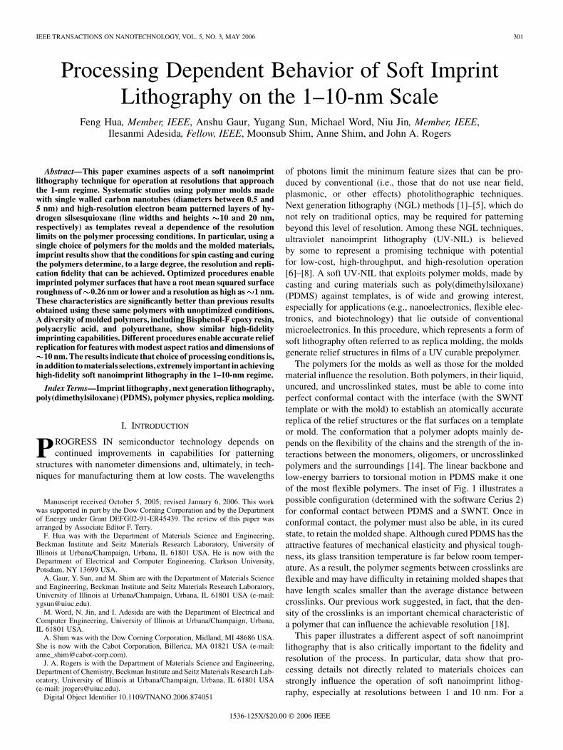
Fig. 1. (Left) Schematic illustration of steps for soft nanoimprint lithography process that uses single-walled carbon nanotubes as templates and ultraviolet curablepolymers to investigate resolution in 1-nm regime. (Right) Illustration of steps for molding structures with lateral and vertical dimensions in 10- and 20-nm regime,respectively.
given set of materials for the molds and the molded films, theachievable resolution can span a wide range, depending on theprocessing conditions. To illustrate these effects, we performedsystematic soft imprint lithography of patterns with criticaldimensions in the 1–10-nm range. For features smaller than
5 nm, single-walled carbon nanotubes served as templatesto generate the PDMS molds [18]. For larger geometries, weused patterns of hydrogen silsesquioxane (HSQ) defined withadvanced forms of direct write electron beam lithography. Weobserved generally that processing procedures, such as speedsfor spin casting and conditions for curing, influence the surfaceroughness in nominally flat regions of the imprinted patternsand, further, that low roughness enables high resolution in repli-cation of lateral feature dimensions. Accurate replication offeature heights relies critically on processing conditions (whichare sometimes different than those that lead to high resolution)that facilitate polymer flow. Systematic studies reveal sets ofconditions that enable 1-nm resolution and accurate reliefreplication for nearly 2:1 aspect ratio features with dimensionsbetween 3 and 20 nm, using several different molded polymers.These results represent considerable improvements over thosepreviously achieved with the same set of materials [18].
II. EXPERIMENTAL METHODS
Fig. 1 shows the two sets of procedures used for the SWNTand HSQ molding experiments. The templates in both cases
were first exposed to a fluorinated silane vapor to create a non-stick surface in the exposed SiO areas of the sample [11]. Ahigh modulus poly(dimethylsiloxane) (h-PDMS) was then spincast and cured on the template surface. A low modulus PDMS(s-PDMS) was poured onto top of this layer and then thermallycured [12], [13]. Peeling the h-PDMS/s-PDMS composite moldaway from the template completed the process. The s-PDMSprovides a soft, physically tough layer that makes the moldseasy to handle. Flood exposing a layer of photocurable polymer,polyurethane (PU), on a silicon wafer to ultraviolet (UV) lightpassing through the PDMS mold cured the polymer into a solidform. In the final step, the PDMS mold was peeled back, leavinga replica of the relief on its surface. In the usual NIL process, auniform etch back follows the molding. The studies presentedhere do not explore this part of the process.
Preparation of Templates: The molecular resolution(1–5 nm) templates consisted of randomly aligned individualSWNTs with diameters between 0.5 and 5 nm and a coverageof 1–10 tubes/ m on SiO /Si wafers. The tubes were grownby methane-based chemical–vapor deposition (CVD) using arelatively high concentration of ferritin catalysts [9], [10]. Aprevious paper describes the details of template preparation[18]. Templates with features larger than 5 nm were producedby advanced forms of electron beam lithography [21]. Inparticular, negative-tone inorganic HSQ on silicon wafers waspatterned by a JOEL (JBX-6000FS) electron beam lithographysystem with an energy of 50 kV. Templates fabricated in this
HUA et al.: PROCESSING DEPENDENT BEHAVIOR OF SOFT IMPRINT LITHOGRAPHY ON 1–10-nm SCALE 303
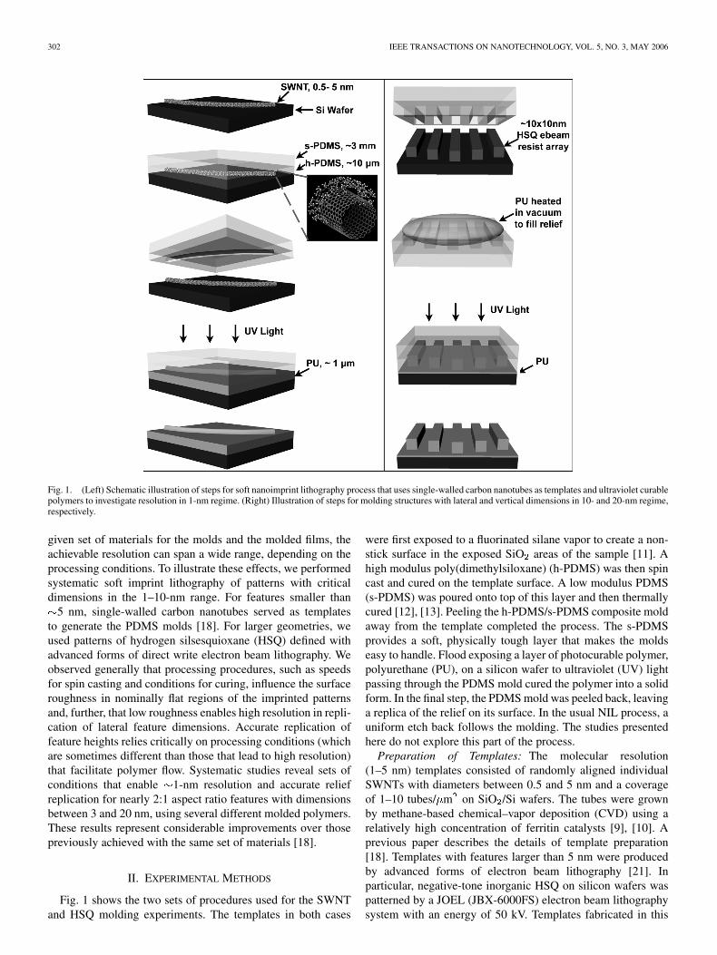
TABLE IFIVE DIFFERENT PROCEDURES FOR CASTING AND CURING h-PDMS
FOR IMPRINT MOLDS AND SURFACE ROUGHNESS ASSOCIATED
WITH MOLDED POLYMERS
manner consisted of arrays of 10-nm-wide lines separated by30 nm, with heights between 3 and 20 nm. Since the line is notuniform in height along its length, it is possible to observe thereplication for aspect ratios between 0.3 and 2.
Investigation of Effect of Spin Speed on Surface Roughnessof Imprinted PU: Liquid PU (NOA 73 from Norland Products;viscosity 130 cps) was spin cast onto silicon wafers at differentspin speeds and imprinted by a flat PDMS mold derived from abare fluorinated silicon surface using processes in Table I. ThePU was completely cured at a dose of 70 J/cm from a UV Hglamp (350–380 nm). The surface roughness of the PU layers wasthen characterized by atomic force microscopy (AFM) usingultra-sharp tips (nanosensors) and identical measurement con-ditions. The vendor specification for the tip radius is 2 nm.The images were collected in tapping mode with a 1-Hz-per-linescan rate and a scan range of 1 1 m.
Investigation of Effect of Spin Speed and Curing Tempera-ture on Surface Roughness of h-PDMS: Table I illustrates fiveprocedures for making the h-PDMS layer of a composite mold,using a bare fluorinated silicon wafer as a template. The overallprocess parameters are the same as those described in [18], butsome of the spin speed, curing temperatures, and times are dif-ferent. After prebaking the h-PDMS, a layer of s-PDMS ma-terial was poured onto the top and cured for 2 h at 65 C. PUlayers (spin cast at 9000 r/min on a silicon wafer and UV curedat a dose of 70 J/cm ) were then imprinted by PDMS moldsprepared using these procedures. AFM analysis determined thesurface roughness of the PU in each case using the proceduresdescribed previously. (Direct AFM measurement of the PDMSelement was not possible, due to the soft, tacky surface charac-teristic of elastomers such as PDMS.)
Molecular Scale Soft Nanoimprint Lithography: We fol-lowed the process that minimized the surface roughness onthe PU: 1) treat the SWNT template surface with silane; 2)spin cast the h-PDMS on the template at 9000 r/min; 3) allowcuring to proceed at room temperature for 24 h; 4) pour on thes-PDMS and cure at 65 C for 2 h; 5) separate the template andPDMS mold; 6) spin cast PU on a silicon wafer at 9000 r/min;7) place a PDMS mold on the PU and flood expose with UVlight at a dose of 70 J/cm ; and 8) peel back the PDMS moldfrom PU surface.
Molecular Simulation of PDMS Conformability toSWNT: Simulations were conducted with the commercial
polymer modeling program, Cerius 2. At the beginning, a tubewas introduced and defined as the rigid body. Monomer unitsof PDMS were added sequentially to form a linked PDMSpolymer structure close to the SWNT. After each additionof each monomer, the system energy was minimized under aconsistent force field (pcff).
Soft Nanoimprint Lithography for Modest Aspect Ratio Fea-tures of HSQ at 10 nm: Two procedures were attempted. Thefirst used a processing sequence similar to that for the SWNTtemplates. After the HSQ template was silanized, h-PDMS wasspin cast on it at 3000 r/min. They were cured at 65 C for 3 min.Then, s-PDMS was poured on and put in 65 C again for 2 h.After the composite PDMS mold was ready, it was peeled backfrom the HSQ template. It was then placed on the liquid PUthat was drop cast on silicon wafer. The PU under the PDMSmold was cured by UV light exposure at room temperature. Thecuring is done in atmosphere. After the PDMS mold was peeledback from the PU, a height loss of the replica was observed.The second, which was observed to improve the accuracy of theheight replication, began by placing the PDMS mold with itsstructured side up and the PU cast directly on top. This structurewas then moved into a vacuum chamber and heated at 80 C for1 h. Placing the PU coated PDMS mold against a silicon wafer,curing the PU with UV light, and then peeling away the PDMSmold completed the process.
III. RESULTS AND DISCUSSIONS
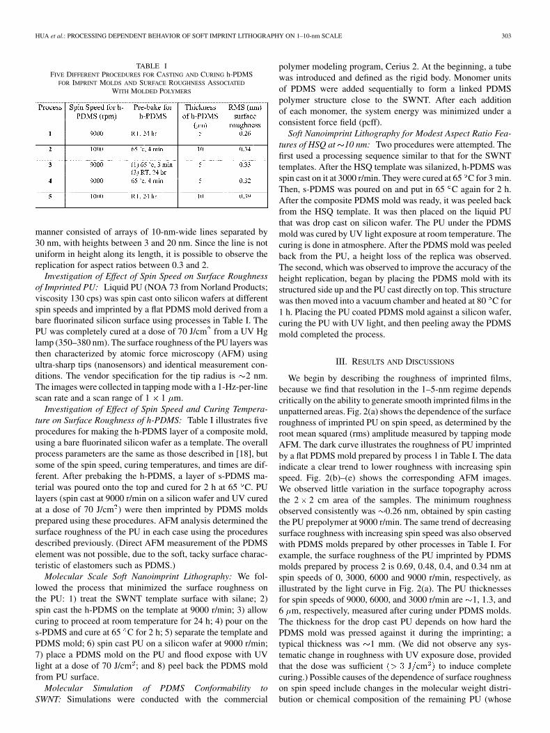
We begin by describing the roughness of imprinted films,because we find that resolution in the 1–5-nm regime dependscritically on the ability to generate smooth imprinted films in theunpatterned areas. Fig. 2(a) shows the dependence of the surfaceroughness of imprinted PU on spin speed, as determined by theroot mean squared (rms) amplitude measured by tapping modeAFM. The dark curve illustrates the roughness of PU imprintedby a flat PDMS mold prepared by process 1 in Table I. The dataindicate a clear trend to lower roughness with increasing spinspeed. Fig. 2(b)–(e) shows the corresponding AFM images.We observed little variation in the surface topography acrossthe 2 2 cm area of the samples. The minimum roughnessobserved consistently was 0.26 nm, obtained by spin castingthe PU prepolymer at 9000 r/min. The same trend of decreasingsurface roughness with increasing spin speed was also observedwith PDMS molds prepared by other processes in Table I. Forexample, the surface roughness of the PU imprinted by PDMSmolds prepared by process 2 is 0.69, 0.48, 0.4, and 0.34 nm atspin speeds of 0, 3000, 6000 and 9000 r/min, respectively, asillustrated by the light curve in Fig. 2(a). The PU thicknessesfor spin speeds of 9000, 6000, and 3000 r/min are 1, 1.3, and6 m, respectively, measured after curing under PDMS molds.The thickness for the drop cast PU depends on how hard thePDMS mold was pressed against it during the imprinting; atypical thickness was 1 mm. (We did not observe any sys-tematic change in roughness with UV exposure dose, providedthat the dose was sufficient J cm to induce completecuring.) Possible causes of the dependence of surface roughnesson spin speed include changes in the molecular weight distri-bution or chemical composition of the remaining PU (whose
304 IEEE TRANSACTIONS ON NANOTECHNOLOGY, VOL. 5, NO. 3, MAY 2006
Fig. 2. (a) Surface roughness for imprinted films of photocurable polyurethane(PU). Dark and light curves represent PU imprinted by PDMS molds preparedby processes 1 and 2 in Table I. (b)–(e). Tapping mode AFM images of PUsurface (imprinted by PDMS mold prepared by process 1 in Table I) which werespin cast at different speeds.
detailed chemical composition is not available from the vendor)or changes in the molecular shape, the degree of ordering orcystallinity, and/or the chain entanglement [15]–[17]. To explorethese possibilities, we performed prism coupling measurementsof the in-plane and out-of-plane indexes of refraction, infraredabsorption spectroscopy on films with different thicknesses,X-ray diffraction, and differential scanning calorimetry (DSC).None of these experiments revealed any significant chemical orstructural differences in any of the samples. For example, theresults of the polarized infrared measurements reveal no depen-dence of the absorption features on processing conditions. Theprism coupling measurements show insignificant differencesbetween the in- and out-of-plane index of refraction, suggestingan absence of structural ordering that could potentially be in-duced by the spin casting. Wide angle X-ray diffraction shows asimilar degree of crystallinity in films coated at 3000, 6000, and9000 r/min, with a somewhat lower crystallinity in the drop castfilms. DSC traces do not reveal any difference in glass transitiontemperature. Thermally excited interfacial capillary waves
provide one possible explanation that is consistent with this setof measurements. This type of effect, when it occurs betweentwo immiscible polymers, can contribute to a broadening ofthe interface. In fact, the interface roughness, between certainpolymers, is found to have a dependence on the film thicknessdue to the capillary waves [22], [23]. Additional work, such asdetailed temperature dependent studies, is required to explorefurther this possibility.
We also investigated the influence of similar processing re-lated conditions for the preparation of the PDMS stamps. Inparticular, sets of experiments were performed with differentcuring temperatures and spin speed deposition conditions forthe h-PDMS. The fluorinated surfaces of bare silicon wafersserved as the templates. Although it was difficult to obtain re-liable AFM measurements from the low modulus surface ofthe PDMS itself, we could examine the roughness of layers ofPU imprinted by the PDMS molds. The flat PDMS molded PUsamples processed using the optimized high-spin speed depo-sition conditions described previously. Among the five PDMSmolds studied in Table I, process 1 generated the smoothest im-printed PU surface, 0.26 nm in roughness. In processes 2–5,the h-PDMS was either spin cast at low spin speeds or cured atelevated temperatures. The results suggest that elevated temper-atures, which provide the polymer chains with significant mo-bility, lead to rough surfaces. Long curing times associated withlow temperatures reduce the roughness, perhaps by providingthe polymer chains with adequate time to relax and conform tothe interfaces.
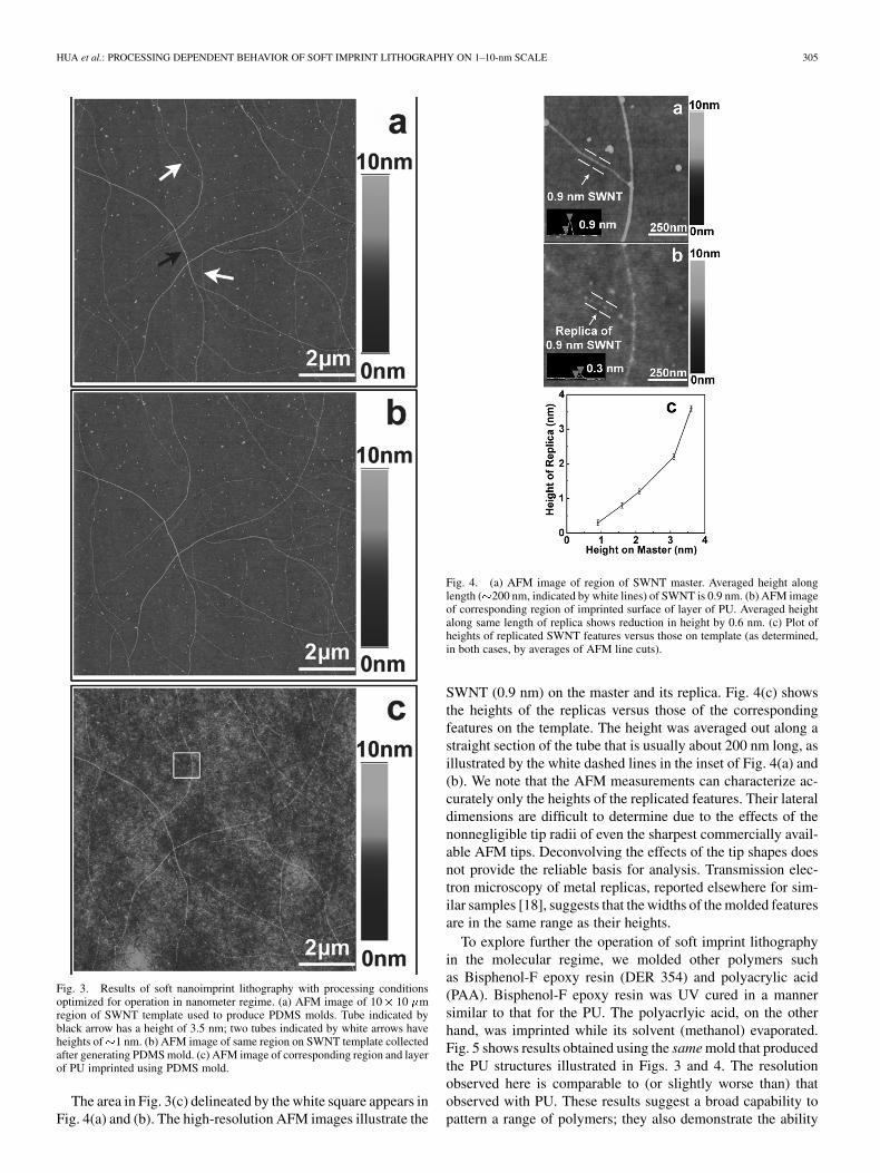
We performed molecular scale imprinting by use of SWNTtemplates and the best procedures for making and using thePDMS molds with PU. Fig. 3(a)–(c) shows AFM images(10 10 m) of a SWNT template, the template after the moldgeneration process, and the imprinted PU surface. Fig. 3(b)shows that the process of generating the molds does not alterAFM observable features of the template (the curled tube thatappears on the template after, but not before, mold generationwas likely transported to the measured area during one of theprocessing or imaging steps). The entire surface of the templateafter use is largely clean and without observable polymericresidue. (At the high resolution that is possible with optimizedconditions, it is possible to observe small amounts of residue inselected regions of the templates.) The image of the PU replica[Fig. 3(c)] shows high fidelity and a capability to replicate,at least partially, the smallest observable SWNTs—diametersslightly less than 1 nm. This result is approximately two timesbetter than our previously reported results. The SWNTs withsizes larger than 1 nm were all reproduced cleanly along theirentire lengths. In particular, the relief structures associated withthe 3.5-nm tubes were fully replicated without loss in height.It is important to note that the small difference between theheights of the SWNTs and the molded features, and especiallythe complete height recovery at 3.5 nm, in the optimizedprocess is consistent with a small effect of the silane layer(used to prevent adhesion between the PDMS and the templateduring mold preparation), either due to incomplete coveragenear the SWNTs or to a partial or fully horizontal orientationof the silane molecules after the PDMS is cast on the substrate[19], [20].
HUA et al.: PROCESSING DEPENDENT BEHAVIOR OF SOFT IMPRINT LITHOGRAPHY ON 1–10-nm SCALE 305
Fig. 3. Results of soft nanoimprint lithography with processing conditionsoptimized for operation in nanometer regime. (a) AFM image of 10� 10 �mregion of SWNT template used to produce PDMS molds. Tube indicated byblack arrow has a height of 3.5 nm; two tubes indicated by white arrows haveheights of�1 nm. (b) AFM image of same region on SWNT template collectedafter generating PDMS mold. (c) AFM image of corresponding region and layerof PU imprinted using PDMS mold.
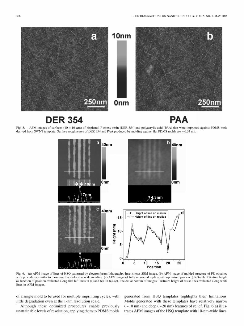
The area in Fig. 3(c) delineated by the white square appears inFig. 4(a) and (b). The high-resolution AFM images illustrate the
Fig. 4. (a) AFM image of region of SWNT master. Averaged height alonglength (�200 nm, indicated by white lines) of SWNT is 0.9 nm. (b) AFM imageof corresponding region of imprinted surface of layer of PU. Averaged heightalong same length of replica shows reduction in height by 0.6 nm. (c) Plot ofheights of replicated SWNT features versus those on template (as determined,in both cases, by averages of AFM line cuts).
SWNT (0.9 nm) on the master and its replica. Fig. 4(c) showsthe heights of the replicas versus those of the correspondingfeatures on the template. The height was averaged out along astraight section of the tube that is usually about 200 nm long, asillustrated by the white dashed lines in the inset of Fig. 4(a) and(b). We note that the AFM measurements can characterize ac-curately only the heights of the replicated features. Their lateraldimensions are difficult to determine due to the effects of thenonnegligible tip radii of even the sharpest commercially avail-able AFM tips. Deconvolving the effects of the tip shapes doesnot provide the reliable basis for analysis. Transmission elec-tron microscopy of metal replicas, reported elsewhere for sim-ilar samples [18], suggests that the widths of the molded featuresare in the same range as their heights.
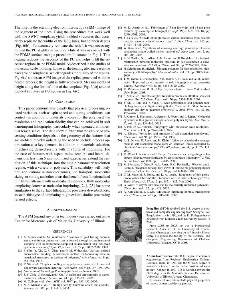
To explore further the operation of soft imprint lithographyin the molecular regime, we molded other polymers suchas Bisphenol-F epoxy resin (DER 354) and polyacrylic acid(PAA). Bisphenol-F epoxy resin was UV cured in a mannersimilar to that for the PU. The polyacrlyic acid, on the otherhand, was imprinted while its solvent (methanol) evaporated.Fig. 5 shows results obtained using the same mold that producedthe PU structures illustrated in Figs. 3 and 4. The resolutionobserved here is comparable to (or slightly worse than) thatobserved with PU. These results suggest a broad capability topattern a range of polymers; they also demonstrate the ability
306 IEEE TRANSACTIONS ON NANOTECHNOLOGY, VOL. 5, NO. 3, MAY 2006
Fig. 5. AFM images of surfaces (10� 10 �m) of bisphenol-F epoxy resin (DER 354) and polyacrylic acid (PAA) that were imprinted against PDMS moldderived from SWNT template. Surface roughnesses of DER 354 and PAA produced by molding against flat PDMS molds are �0.34 nm.
Fig. 6. (a) AFM image of lines of HSQ patterned by electron beam lithography. Inset shows SEM image. (b) AFM image of molded structure of PU obtainedwith procedures similar to those used in molecular scale molding. (c) AFM image of fully recovered replica with optimized process. (d) Graph of feature heightas function of position evaluated along first left lines in (a) and (c). In (a)–(c), line cut at bottom of images illustrates height of resist lines evaluated along whitelines in AFM images.
of a single mold to be used for multiple imprinting cycles, withlittle degradation even at the 1-nm resolution scale.
Although these optimized procedures enable previouslyunattainable levels of resolution, applying them to PDMS molds
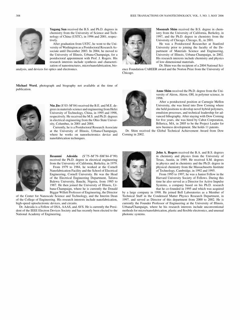
generated from HSQ templates highlights their limitations.Molds generated with these templates have relatively narrow( 10 nm) and deep ( 20 nm) features of relief. Fig. 6(a) illus-trates AFM images of the HSQ template with 10-nm-wide lines.
HUA et al.: PROCESSING DEPENDENT BEHAVIOR OF SOFT IMPRINT LITHOGRAPHY ON 1–10-nm SCALE 307
The inset is the scanning electron microscopy (SEM) image ofthe segment of the lines. Using the procedures that work wellwith the SWNT templates yields molded structures that accu-rately replicate the widths of the HSQ lines, but not their depths[Fig. 6(b)]. To accurately replicate the relief, it was necessaryto heat the PU slightly in vacuum while it was in contact withthe PDMS surface, using a procedure illustrated in Fig. 1. Thisheating reduces the viscosity of the PU and helps it fill the re-cessed regions in the PDMS mold. As described in the studies ofmolecular scale molding, however, the heating also increases thebackground roughness, which degrades the quality of the replica.Fig. 6(c) shows an AFM image of the replica generated with theheated process; the height is fully recovered. Measurements ofheight along the first left line of the template [Fig. 6(d)] and themolded structure in PU appear in Fig. 6(c).
IV. CONCLUSION
This paper demonstrates clearly that physical processing re-lated variables, such as spin speed and curing conditions, cancontrol (in addition to materials choices for the polymers) theresolution and replication fidelity that can be achieved in softnanoimprint lithography, particularly when operated at molec-ular length scales. The data show, further, that the choice of pro-cessing conditions depends on the geometry of the features thatare molded, thereby indicating the need to include process op-timization as a key element, in addition to materials selection,in achieving desired results with this form of imprinting. Forthe case of features with aspect ratios near 1:1 and lateral di-mensions less than 5 nm, optimized approaches extend the res-olution of this technique into the single nanometer resolutionregime, with a variety of polymers. This capability will likelyfind applications in nanoelectronics, ion transport, molecularsizing, or sorting and other areas that benefit from functionalizedthin films patterned with molecular dimensions. Bulk moleculartemplating, known as molecular imprinting, [24], [25], has somesimilarities to the surface lithographic processes described here;as such, this type of templating might exhibit similar processingrelated effects.
ACKNOWLEDGMENT
The AFM (or/and any other techniques) was carried out in theCenter for Microanalysis of Materials, University of Illinois.
REFERENCES
[1] A. Kumar and G. M. Whitesides, “Features of gold having microm-eter to centimeter dimensions can be formed through a combination ofstamping with an elastomeric stamp and an alkanethiol “ink” followedby chemical etching,” Appl. Phys. Lett., vol. 63, pp. 2002–2004, 1993.
[2] E. Kim, Y. Xia, X. M. Zhao, and G. M. Whitesides, “Solvent-assistedmicrocontact molding: A convenient method for fabricating three-di-mensional structures on surfaces of polymers,” Adv. Mater., vol. 9, pp.651–654, 1997.
[3] Y. Xia et al., “Replica molding using polymeric materials: A practicalstep toward nanomanufacturing,” Adv. Mater., vol. 9, pp. 147–149, 1997.
[4] International Technology Roadmap for Semiconductors, 2003.[5] S. Y. Chou, C. Keimel, and J. Gu, “Ultrafast and direct imprint of nanos-
tructures in silicon,” Nature, vol. 417, pp. 835–837, 2002.[6] M. Colburn et al., Proc. SPIE, vol. 3997, pp. 453–457, 2000.[7] N. A. Melosh et al., “Ultrahigh density nanowire lattices and circuits,”
Science, vol. 300, pp. 112–114, 2003.
[8] M. D. Austin et al., “Fabrication of 5 nm linewidth and 14 nm pitchfeatures by nanoimprint lithography,” Appl. Phys. Lett., vol. 84, pp.5299–5301, 2004.
[9] Y. Li et al., “Growth of single-walled carbon nanotubes from discretecatalytic nanoparticles of various sizes,” J. Phys. Chem., vol. 105, pp.11 424–11 431, 2001.
[10] W. Kim et al., “Synthesis of ultralong and high percentage of semi-conducting single-walled carbon nanotubes,” Nano Lett., vol. 2, pp.703–708, 2002.
[11] A. N. Parikh, D. L. Allara, I. B. Azouz, and F. Rondelez, “An intrinsicrelationship between molecular structure in self-assembled n-alkyl-siloxane monolayers,” J. Phys. Chem., vol. 98, pp. 7577–7590, 1994.
[12] H. Schmid and B. Michel, “Siloxane polymers for high-resolution, high-accuracy soft lithography,” Macromolecules, vol. 33, pp. 3042–3049,2000.
[13] T. W. Odom, J. Christopher, D. B. Wolfe, K. E. Paul, and G. M. White-sides, “Improved pattern transfer in soft lithography using compositestamps,” Langmuir, vol. 18, pp. 5314–5320, 2002.
[14] M. Rubinstein and R. H. Colby, Polymer Physics. New York: OxfordUniv. Press, 2003.
[15] S. Sills et al., “Interfacial glass transition profiles in ultrathin, spin castpolymer films,” J. Chem. Phys., vol. 120, pp. 5334–5338, 2004.
[16] Y. Shi, J. Liu, and Y. Yang, “Device performance and polymer mor-phology in polymer light emitting diodes: The control of thin film mor-phology and device quantum efficiency,” J. Appl. Phys., vol. 87, pp.4254–4263, 2000.
[17] F. Kremer, L. Hartmann, A. Serghei, P. Pouret, and L. Léger, “Moleculardynamics in thin grafted and spin-coated polymer layers,” Eur. Phys. J.E., vol. 12, pp. 139–142, 2003.
[18] F. Hua et al., “Imprint lithography with molecular-scale resolution,”Nano Lett., vol. 4, pp. 2467–2471, 2004.
[19] A. Ulman, “Formation and structure of self-assembled monolayers,”Chem. Rev., vol. 96, pp. 1533–1554, 1996.
[20] A. S. Duwez, U. Jonas, and H. Klein, “Influence of molecular arrange-ment in self-assembled monolayers on adhesion forces measured bychemical force microscopy,” ChemPhyschem., vol. 4, pp. 1107–1111,2003.
[21] M. Word, I. Adesida, and P. Berger, “Nanometer-period gratings in hy-drogen silsesquioxane fabricated by electron beam lithography,” J. Vac.Sci. Technol., vol. B21, pp. L12–L15, 2003.
[22] M. Sferrazza, C. Xiao, R. A. L. Jones, D. G. Bucknall, J. Webster, and J.Penfold, “Evidence for capillary waves at immiscible polymer/polymerinterfaces,” Phys. Rev. Lett., vol. 78, pp. 3693–3696, 1997.
[23] C. M. Mate, M. F. Toney, and K. A. Leach, “Roughness of thin perflu-oropolyether lubricant films: Influence on disk drive technology,” IEEETrans. Magn., vol. 37, no. 3, pp. 1821–1823, May 2001.
[24] G. Wulff, “Enzyme-like catalysis by molecularly imprinted polymers,”Chem. Rev., vol. 102, pp. 1–28, 2002.
[25] A. Katz and M. E. Davis, “Molecular imprinting of bulk, microporoussilica,” Nature, vol. 403, pp. 286–289, 2000.
Feng Hua (M’04) received the B.S. degree in elec-trical and computer engineering from Shanghai JiaoTong University, in 1990, and the Ph.D. degree in en-gineering from Louisiana Tech University, Ruston, in2003.
From 2003 to 2005, he was a PostdoctoralResearch Associate at the University of Illinois,Urbana-Champaign, working on soft imprint lithog-raphy. He joined the faculty of the Electrical andComputer Engineering Department of ClarksonUniversity, Potsdam, NY, in 2005.
Anshu Gaur received the B.E. degree in ceramicsengineering from Regional Engineering College,Rourkela, India, in 1999, and the M.Tech. degree inmaterials science from the Indian Institute of tech-nology, Kanpur, in 2001. He is working toward thePh.D. degree in the Materials Science Department,University of Illinois, Urbana-Champaign.
His research interests include physical propertiesof nanostructures and device physics.
308 IEEE TRANSACTIONS ON NANOTECHNOLOGY, VOL. 5, NO. 3, MAY 2006
Yugang Sun received the B.S. and Ph.D. degrees inchemistry from the University of Science and Tech-nology of China (USTC), in 1996 and 2001, respec-tively.
After graduation from USTC, he went to the Uni-versity of Washington as a Postdoctoral Research As-sociate until December 2003. In 2004, he moved tothe University of Illinois, Urbana-Champaign, for apostdoctoral appointment with Prof. J. Rogers. Hisresearch interests include synthesis and characteri-zation of nanostructures, micro/nanofabrication, bio-
analysis, and devices for optics and electronics.
Michael Word, photograph and biography not available at the time ofpublication.
Niu Jin (S’03–M’04) received the B.E. and M.E. de-grees in materials science and engineering from HefeiUniversity of Technology, China, in 1995 and 1998,respectively. He received the M.S. and Ph.D. degreesin electrical engineering from the Ohio State Univer-sity, Columbus, in 2001 and 2004.
Currently, he is a Postdoctoral Research Associateat the University of Illinois, Urbana-Champaign,where he works on nanoelectronics device andnanofabrication techniques.
Ilesanmi Adesida (S’75–M’79–SM’84–F’99)received the Ph.D. degree in electrical engineeringfrom the University of California, Berkeley, in 1979.
From 1979 to 1984, he worked at the CornellNanofabrication Facility and the School of ElectricalEngineering, Cornell University. He was the Headof the Electrical Engineering Department, TafawaBalewa University, Bauchi, Nigeria, from 1985 to1987. He then joined the University of Illinois, Ur-bana-Champaign, where he is currently the DonaldBiggar Willett Professor of Engineering, the Director
of the Center for Nanoscale Science and Technology, and the Interim Deanof the College of Engineering. His research interests include nanofabrication,high-speed optoelectronic devices, and circuits.
Dr. Adesida is a Fellow of OSA, AAAS, and AVS. He is currently the Presi-dent of the IEEE Electron Devices Society and has recently been elected to theNational Academy of Engineering.
Moonsub Shim received the B.S. degree in chem-istry from the University of California, Berkeley, in1997, and the Ph.D. degree in chemistry from theUniversity of Chicago, Chicago, IL, in 2001.
He was a Postdoctoral Researcher at StanfordUniversity prior to joining the faculty of the De-partment of Materials Science and Engineering,University of Illinois, Urbana-Champaign, in 2002.His research interests include chemistry and physicsof low-dimensional materials.
Dr. Shim was the recipient of a 2004 National Sci-ence Foundation CAREER award and the Norton Prize from the University ofChicago.
Anne Shim received the Ph.D. degree from the Uni-versity of Akron, Akron, OH, in polymer science, in1998.
After a postdoctoral position at Carnegie MellonUniversity, she was hired into Dow Corning whereshe held positions to develop novel hybrid polymers,emulsion processes, and technical leadership for ad-vanced lithography. After staying with Dow Corningfor five years, she was hired by Cabot Corporation,Billerica, MA, in 2005 to be the Project Leader fornew business development. She holds 11 patents.
Dr. Shim received the Global Technical Achievement Award from DowCorning in 2002.
John A. Rogers received the B.A. and B.S. degreesin chemistry and physics from the University ofTexas, Austin, in 1989. He received S.M. degreesin physics and in chemistry and the Ph.D. degree inphysical chemistry from the Massachusetts Instituteof Technology, Cambridge, in 1992 and 1995.
From 1995 to 1997, he was a Junior Fellow in theHarvard University Society of Fellows. During thistime he also served as a Director for Active ImpulseSystems, a company based on his Ph.D. researchthat he co-founded in 1995 and which was acquired
by a large company in 1998. He joined Bell Laboratories as a Member ofTechnical Staff in the Condensed Matter Physics Research Department, in1997, and served as Director of this department from 2000 to 2002. He iscurrently the Founder Professor of Engineering at the University of Illinois,Urbana/Champaign, where he his research interests include unconventionalmethods for micro/nanofabrication, plastic and flexible electronics, and unusualphotonic systems.
Related Documents