© Fraunhofer IPMS PROCESS TECHNOLOGIES FOR ADVANCED ORGANIC ELECTRONIC DEVICES: MICRODISPLAYS, LIGHTING AND SOLAR CELLS Dr. Christian May Fraunhofer IPMS - Center for Organic Materials and Electronic Devices Dresden COMEDD Innovations for Industry – at MicroNanoTec, Hannover, April 20 th , 2010

Welcome message from author
This document is posted to help you gain knowledge. Please leave a comment to let me know what you think about it! Share it to your friends and learn new things together.
Transcript

© Fraunhofer IPMS
PROCESS TECHNOLOGIES FOR ADVANCED ORGANIC
ELECTRONIC DEVICES:
MICRODISPLAYS, LIGHTING AND SOLAR CELLS
Dr. Christian May
Fraunhofer IPMS - Center for Organic Materials and Electronic Devices Dresden COMEDD
Innovations for Industry– at MicroNanoTec,Hannover, April 20th, 2010

© Fraunhofer IPMS
OUTLINE
� COMEDD introduction
� OLED basics
� OLED lighting
� Pilot line for substrates 370 x 470 mm²
� R2R fabrication of OLED
� Organic solar cells
� ZnPc:C60 tandem cell
� Transparent organic solar cell
� OLED-on-CMOS
� VGA OLED microdisplay
� COMEDD offer and network

© Fraunhofer IPMS
COMEDD as trademark of Fraunhofer IPMS
� Opened in 200
investments of about 30 M€ (EU, Sachsen, FhG)
Mission
� Customer and Application Specific Research, Development and
Pilot fabrication on novel device concepts and manufacturing
methods in the field of organic electronics (small molecule)
Infrastructure
� Clean room 900 m², Labs 100 m²
Fabrication lines
� Pilot line Gen2 (370 x 470 mm²)
� Pilot line OLED-on-CMOS (200x200 mm²)
� Roll-to-Roll line (300 mm foils)
CENTER FOR ORGANIC MATERIALS AND ELECTRONIC DEVICES
DRESDEN
© Fraunhofer IPMS
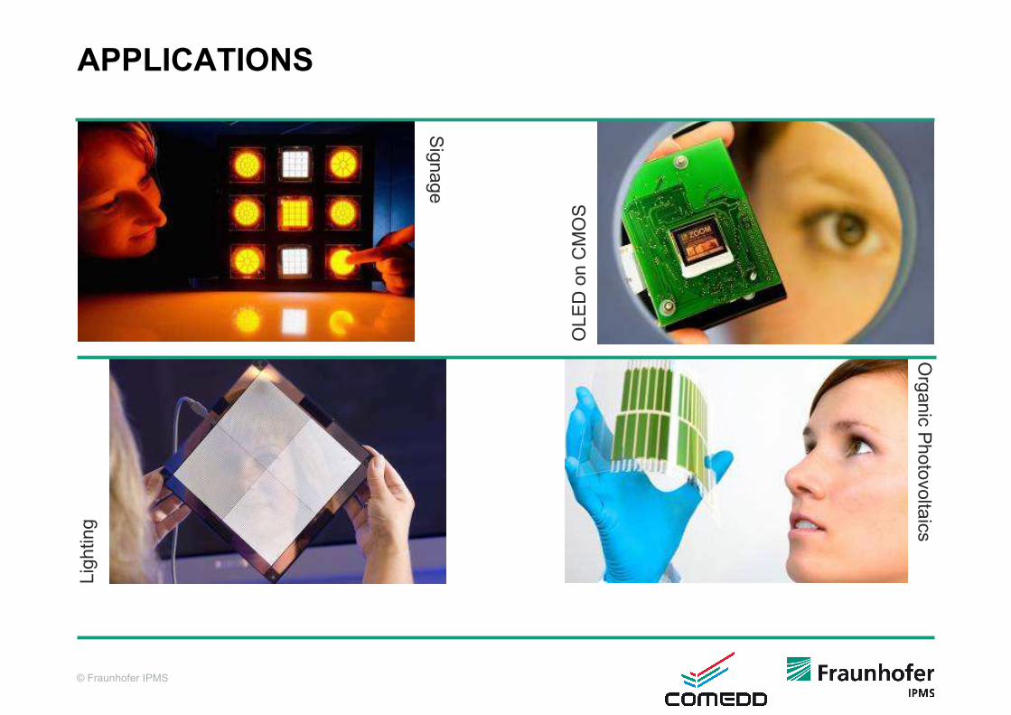
APPLICATIONS
Sig
nag
eO
LE
D o
n C
MO
S
Lig
hting
Org
anic
Ph
oto
volta
ics
© Fraunhofer IPMS
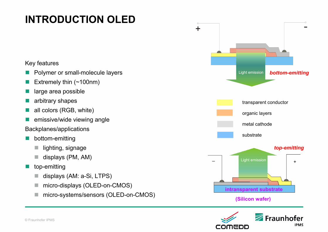
Light emission +_
bottom-emitting
top-emitting
intransparent substrate
transparent conductor
organic layers
metal cathode
substrate
Light emission
(Silicon wafer)
INTRODUCTION OLED
Key features
� Polymer or small-molecule layers
� Extremely thin (~100nm)
� large area possible
� arbitrary shapes
� all colors (RGB, white)
� emissive/wide viewing angle
Backplanes/applications
� bottom-emitting
� lighting, signage
� displays (PM, AM)
� top-emitting
� displays (AM: a-Si, LTPS)
� micro-displays (OLED-on-CMOS)
� micro-systems/sensors (OLED-on-CMOS)
© Fraunhofer IPMS
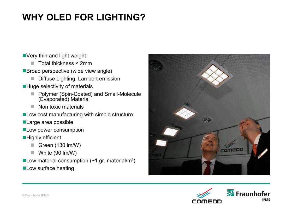
WHY OLED FOR LIGHTING?
�Very thin and light weight
� Total thickness < 2mm
�Broad perspective (wide view angle)
� Diffuse Lighting, Lambert emission
�Huge selectivity of materials
� Polymer (Spin-Coated) and Small-Molecule (Evaporated) Material
� Non toxic materials
�Low cost manufacturing with simple structure
�Large area possible
�Low power consumption
�Highly efficient
� Green (130 lm/W)
� White (90 lm/W)
�Low material consumption (~1 gr. material/m²)
�Low surface heating
© Fraunhofer IPMS
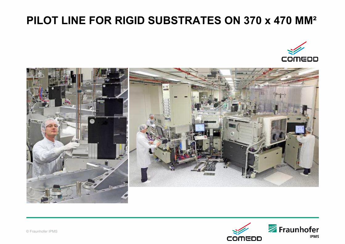
PILOT LINE FOR RIGID SUBSTRATES ON 370 x 470 MM²

© Fraunhofer IPMS
OLED ON GEN2-SUBSTRATES - EFFICIENCY @ 1000 CD/M²
8.8 cd/A43.8 cd/A23.9 cd/A
blue (0.14/0.20)green (0.38/0.58)orange (0.63/0.37)
470 mm370 mm

© Fraunhofer IPMS
OLED ON PHOTOLITOGRAPHY FREE SUBSTRATES
Active OLED area up to 50x50 mm2
Test Layout Demonstrator SO-Light
Gen2 Substrates 470x370 mm2
Structuring by Screen Printing and Laser Ablation
Small Molecule Deposition by Thermal Evaporation
Active OLED area 100x50 mm2

© Fraunhofer IPMS
OLED SIGNAGE APPLICATIONS
OLED steering wheel
OLED nameplate
© Fraunhofer IPMS
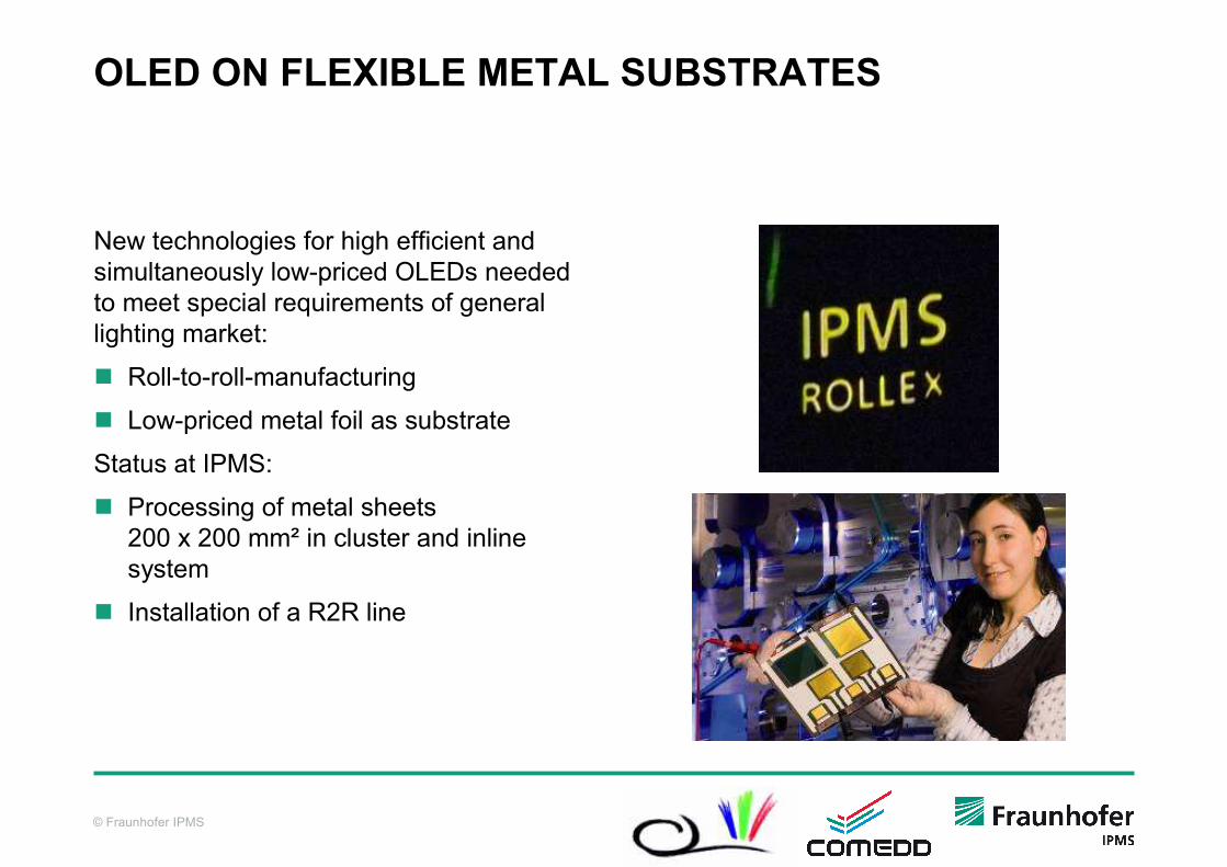
OLED ON FLEXIBLE METAL SUBSTRATES
New technologies for high efficient and
simultaneously low-priced OLEDs needed
to meet special requirements of general
lighting market:
� Roll-to-roll-manufacturing
� Low-priced metal foil as substrate
Status at IPMS:
� Processing of metal sheets
200 x 200 mm² in cluster and inline
system
� Installation of a R2R line

© Fraunhofer IPMS
ROLL TO ROLL VACUUM COATER ROLLEX 300
Attachement possibilityfor an inert shuttle
Winding unit
Deposition cylinder

© Fraunhofer IPMS
ORGANIC SOLAR CELLS
� Total thickness: < 1 µm
� Highly flexible
� High freedom in color and shape
� Only small amounts of org. materials are required (< 1g/m2)
� Cost effective production due to close to room temperature processes
� Large area coating
� Production technologies similar to SM OLEDs
� Short energy payback time(~ 1 year (estimated))
© Fraunhofer IPMS
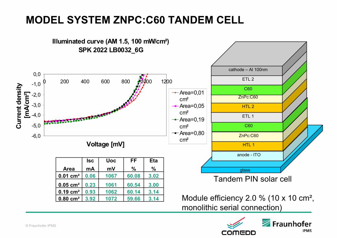
MODEL SYSTEM ZNPC:C60 TANDEM CELL
Tandem PIN solar cell
Module efficiency 2.0 % (10 x 10 cm²,
monolithic serial connection)
anode - ITO
HTL 1
ZnPc:C60
C60
ETL 1
HTL 2
ZnPc:C60
C60
ETL 2
cathode – Al 100nm
glass
Illuminated curve (AM 1.5, 100 mW/cm²)
SPK 2022 LB0032_6G
-6,0
-5,0
-4,0
-3,0
-2,0
-1,0
0,0
0 200 400 600 800 1000 1200
Voltage [mV]
Current density
[mA/cm²] Area=0,01
cm²
Area=0,05
cm²
Area=0,19
cm²
Area=0,80
cm²
3.92
0.93
0.23
0.06
Isc
mA
1072
1062
1061
1067
Uoc
mV
59.66
60.14
60.54
60.08
FF
%
3.14
3.14
3.00
3.02
Eta
%
0.80 cm²
0.19 cm²
0.05 cm²
0.01 cm²
Area

© Fraunhofer IPMS
Illuminated curve (AM 1.5, 100 mW/cm²)
SPK 2023 LB0032_4L
-4,0
-3,0
-2,0
-1,0
0,0
1,0
2,0
3,0
-1000 -500 0 500 1000
voltage [mV]
current density
[mA/cm²]
TRANSPARENT ORGANIC SOLAR CELL
Uoc =922 mVJsc = 3,5 mA/ cm²FF = 54,3 %Eff = 1.8 %Area= 0.19 cm²
400 600 8000
5
10
15
20
25
30
35
40
Tra
nsm
issio
n [
%]
Wavelength [nm]
© Fraunhofer IPMS
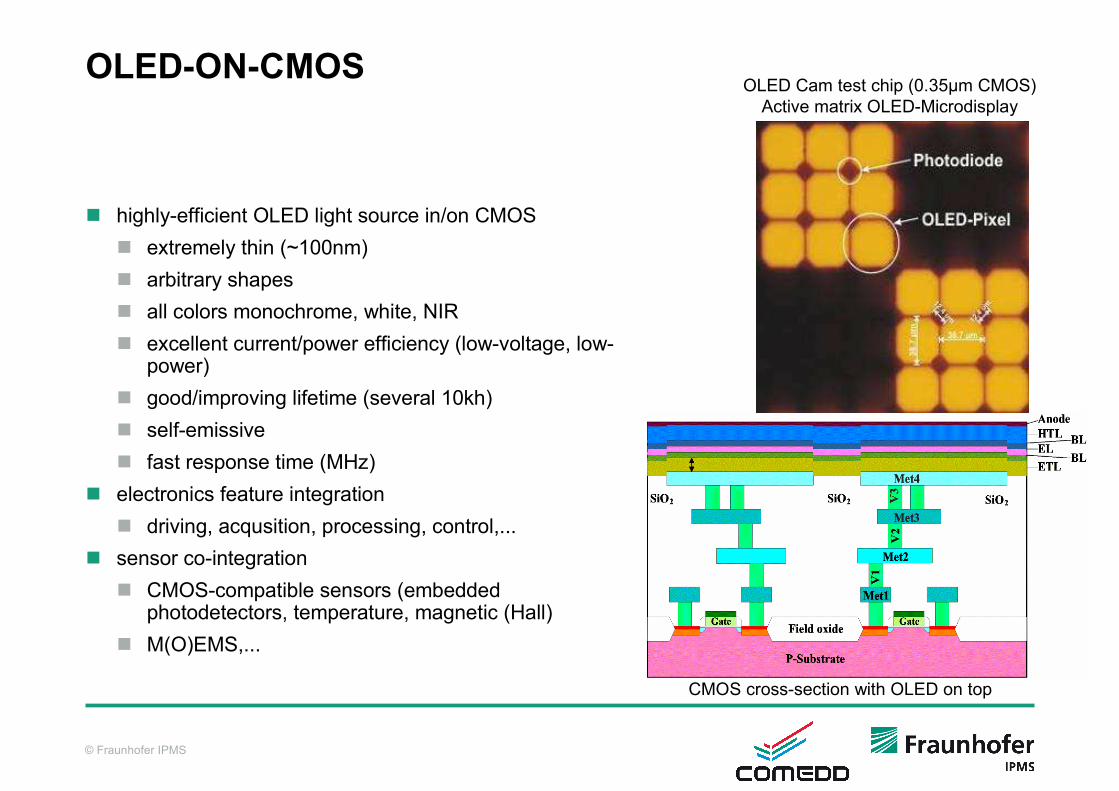
CMOS cross-section with OLED on top
OLED-ON-CMOS
� highly-efficient OLED light source in/on CMOS
� extremely thin (~100nm)
� arbitrary shapes
� all colors monochrome, white, NIR
� excellent current/power efficiency (low-voltage, low-power)
� good/improving lifetime (several 10kh)
� self-emissive
� fast response time (MHz)
� electronics feature integration
� driving, acqusition, processing, control,...
� sensor co-integration
� CMOS-compatible sensors (embedded photodetectors, temperature, magnetic (Hall)
� M(O)EMS,...
OLED Cam test chip (0.35µm CMOS)
Active matrix OLED-Microdisplay

© Fraunhofer IPMS
VGA OLED MICRODISPLAY
� colour VGA (640x480) OLED
microdisplay
� active area 7.68 x 5.76 mm² (chip size
12 x 11 mm²)
� High brightness: 1,000 nits for RGB
colour (HMD)
� see talk by M. Scholles,
Friday, April 23th at MST Vision session

© Fraunhofer IPMS
Europe‘s leading Organic-Cluster - from research to products
www.oes-net.de – please visit OES in hall 2, booth C 37
materials
modeling
organic
technologyTools Products
ORGANIC ELECTRONICS SAXONY

© Fraunhofer IPMS
COMEDD OFFER FOR CUSTOMERS
Integration technologyFabrication technology
Product related R&D Pilot production
FOR
ORGANIC
DEVICES

© Fraunhofer IPMS
COOPERATION OFFER
OLED allow the high efficient generation of
light on several substrate types
COMEDD Gen2 pilot line is available from
now
Metal strips and roll to roll deposition have
the potential for low cost production of
lighting devices
Further potential for OLED on CMOS on
OPV application as well
COMEDD @ Fraunhofer IPMS wants to be
your partner for research, development and
pilot fabrication in this novel device
technology area.
Thank you for your attention!
COMEDD
We shape the light.
Related Documents


