Paper submitted within the scope of the Master’s Thesis Master of Industrial Sciences GROUP T – Leuven Engineering College – 2009-2010 Process Risk Assessment of Semiconductor Wet Chemical Cleaning Techniques Danhua Yao * , Alain Pardon † , Nausikaä Van Hoornick † , Patrick Lievens ‡ *Master student <Biochemical Engineering, focus Medical Bio-engineering>, GROUP T – Leuven Engineering College, Vesaliusstraat 13, 3000 Leuven †<IMEC>, <Kapeldreef 75 B-3001 Leuven Belgium> ‡Unit <matter>, GROUP T – Leuven Engineering College, Vesaliusstraat 13, 3000 Leuven, <[email protected]> Abstract In semiconductor manufacturing industry, a wide range of hazardous chemicals are involved, which have the potential to cause harm to persons, property, or environment. Therefore it is necessary and important to do the process risk assessment of semiconductor manufacturing techniques. This paper is focusing on one of the most important steps in semiconductor industry-Wet Chemical Cleaning, which is happening throughout the whole fabrication process. For the process risk assessment, hazards should be identified and the corresponding actions should be taken to avoid reoccurrence and to achieve the common goal of having healthy and safe working conditions in an environmentally friendly semiconductor industry. Keywords: Risk Assessment, Wet Chemical Cleaning Techniques, Hazardous Chemicals, Health Effects Introduction Because of the producing requirement of semiconductor manufacturing, various small amounts of chemicals are involved, among which some are special gases (some are flammable and others toxic) others are liquid chemicals such as strong acids or alkalines and organic solvents. If these gases or liquids are not treated properly after the producing process, damages or even disasters can be produced. Audits of the occupational hazard in semiconductor manufacturing industry in recent years show that above 90% of the hazards are composed of unsafe behaviors. Hence, not only hardware stability but also software aspects (safety management) should be maintained and improved. A complete enterprising safety management system is composed of several key factors, none of which can be lost to operate as a management chain. In this chain, risk assessment is the vital component. In order to achieve enterprising safety production and maximize return, an adequate effective risk assessment method should be selected. From the variety of methods, Quantitative Risk Assessment is the most scientific and modernized one at present and widely accepted and applied all around the world. [1] For one of the most important steps in the semiconductor manufacturing industry-The Wet Chemical Cleaning, various hazardous liquid solutions and gases are commonly involved as important roles in daily operation, such as hydrochloric acid, sulfuric acid, ammonia hydroxide and ozonated water. These aqueous solutions can emit corresponding gases that are harmful to the workers and the environment. Therefore it is necessary and important to do the quantitative risk assessment of the Wet Chemical Cleaning techniques.

Welcome message from author
This document is posted to help you gain knowledge. Please leave a comment to let me know what you think about it! Share it to your friends and learn new things together.
Transcript

Paper submitted within the scope of the Master’s Thesis Master of Industrial Sciences
GROUP T – Leuven Engineering College – 2009-2010
Process Risk Assessment of Semiconductor Wet Chemical Cleaning Techniques
Danhua Yao*, Alain Pardon
†, Nausikaä Van Hoornick
†, Patrick Lievens
‡
*Master student <Biochemical Engineering, focus Medical Bio-engineering>, GROUP T – Leuven Engineering College,
Vesaliusstraat 13, 3000 Leuven
†<IMEC>, <Kapeldreef 75 B-3001 Leuven Belgium>
‡Unit <matter>, GROUP T – Leuven Engineering College, Vesaliusstraat 13, 3000 Leuven, <[email protected]>
Abstract
In semiconductor manufacturing industry, a wide range of hazardous chemicals are involved, which have the potential to
cause harm to persons, property, or environment. Therefore it is necessary and important to do the process risk assessment
of semiconductor manufacturing techniques. This paper is focusing on one of the most important steps in semiconductor
industry-Wet Chemical Cleaning, which is happening throughout the whole fabrication process. For the process risk
assessment, hazards should be identified and the corresponding actions should be taken to avoid reoccurrence and to
achieve the common goal of having healthy and safe working conditions in an environmentally friendly semiconductor
industry.
Keywords:
Risk Assessment, Wet Chemical Cleaning Techniques, Hazardous Chemicals, Health Effects
Introduction
Because of the producing requirement of semiconductor
manufacturing, various small amounts of chemicals are
involved, among which some are special gases (some are
flammable and others toxic) others are liquid chemicals
such as strong acids or alkalines and organic solvents. If
these gases or liquids are not treated properly after the
producing process, damages or even disasters can be
produced. Audits of the occupational hazard in
semiconductor manufacturing industry in recent years
show that above 90% of the hazards are composed of
unsafe behaviors. Hence, not only hardware stability but
also software aspects (safety management) should be
maintained and improved.
A complete enterprising safety management system is
composed of several key factors, none of which can be
lost to operate as a management chain. In this chain, risk
assessment is the vital component. In order to achieve
enterprising safety production and maximize return, an
adequate effective risk assessment method should be
selected. From the variety of methods, Quantitative Risk
Assessment is the most scientific and modernized one at
present and widely accepted and applied all around the
world. [1]
For one of the most important steps in the semiconductor
manufacturing industry-The Wet Chemical Cleaning,
various hazardous liquid solutions and gases are
commonly involved as important roles in daily operation,
such as hydrochloric acid, sulfuric acid, ammonia
hydroxide and ozonated water. These aqueous solutions
can emit corresponding gases that are harmful to the
workers and the environment. Therefore it is necessary
and important to do the quantitative risk assessment of the
Wet Chemical Cleaning techniques.

2
This paper consists of four parts. The first part covers the
principle of the risk assessment, the second part covers
the general shape of the semiconductor manufacturing
process, the third part covers the in-depth study of the Wet
Chemical cleaning techniques, and the last part covers the
actual quantitative risk assessment.
1. Principle of Risk Assessment
What is risk assessment?
Hazards: A hazard is a situation that poses a level of threat
to life, health, property, or environment. [2] And it has the
intrinsic potential to do harm to human beings.
Risk: A risk is the chance or probability that a person will
be harmed or experience an adverse health effect if
exposed to a hazard. It may also apply to situations with
property or equipment loss. [3]
Risk assessment:
Risk assessment is the process where you:
Identify hazards;
Analyze or evaluate the risk associated with that
hazard;
Determine appropriate ways to eliminate or
control the hazard. [3]
2. Semiconductor Processing
In order to make a comprehensive quantitative risk
assessment of semiconductor Wet Chemical Cleaning
techniques, it is important to have a clarified overview of
the whole IC-manufacturing process.
IC-manufacturing process is a multiple-step sequence of
photographic and chemical processing steps during which
electronic circuits are gradually created on a wafer made
of pure semiconducting material. [4] Figure 1 illustrates
one cycle of the main steps and their sequence. [5] The
final products will come out after repeating several times
this basic cycle. And wafer cleaning is happening
throughout the whole fabrication process.
Figure 1: IC-devices manufacturing process [5]
The main steps of the whole semiconductor
manufacturing will be briefly discussed in this chapter,
except the wafer cleaning techniques which is the main
part of the rest of this paper, and will be specifically
discussed in chapter 3.
2.1. Layering
Layering techniques are used to grow thin layers of film
on the surface of a silicon wafer [6].
In general, there are two primary techniques for layer
deposition: chemical vapor deposition (CVD) and
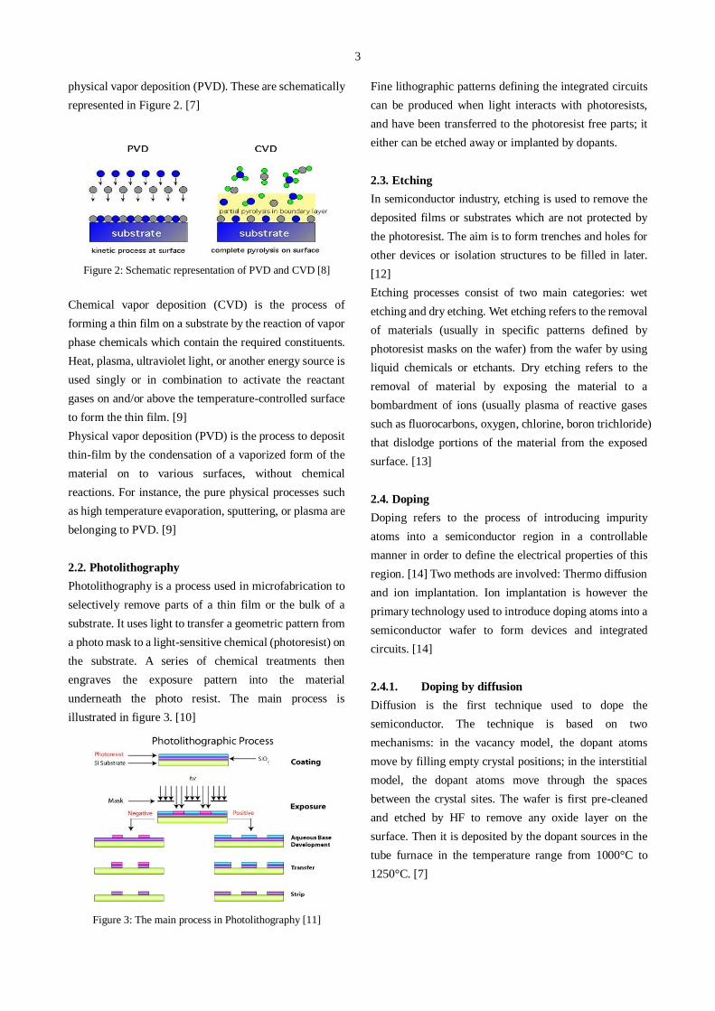
3
physical vapor deposition (PVD). These are schematically
represented in Figure 2. [7]
Figure 2: Schematic representation of PVD and CVD [8]
Chemical vapor deposition (CVD) is the process of
forming a thin film on a substrate by the reaction of vapor
phase chemicals which contain the required constituents.
Heat, plasma, ultraviolet light, or another energy source is
used singly or in combination to activate the reactant
gases on and/or above the temperature-controlled surface
to form the thin film. [9]
Physical vapor deposition (PVD) is the process to deposit
thin-film by the condensation of a vaporized form of the
material on to various surfaces, without chemical
reactions. For instance, the pure physical processes such
as high temperature evaporation, sputtering, or plasma are
belonging to PVD. [9]
2.2. Photolithography
Photolithography is a process used in microfabrication to
selectively remove parts of a thin film or the bulk of a
substrate. It uses light to transfer a geometric pattern from
a photo mask to a light-sensitive chemical (photoresist) on
the substrate. A series of chemical treatments then
engraves the exposure pattern into the material
underneath the photo resist. The main process is
illustrated in figure 3. [10]
Figure 3: The main process in Photolithography [11]
Fine lithographic patterns defining the integrated circuits
can be produced when light interacts with photoresists,
and have been transferred to the photoresist free parts; it
either can be etched away or implanted by dopants.
2.3. Etching
In semiconductor industry, etching is used to remove the
deposited films or substrates which are not protected by
the photoresist. The aim is to form trenches and holes for
other devices or isolation structures to be filled in later.
[12]
Etching processes consist of two main categories: wet
etching and dry etching. Wet etching refers to the removal
of materials (usually in specific patterns defined by
photoresist masks on the wafer) from the wafer by using
liquid chemicals or etchants. Dry etching refers to the
removal of material by exposing the material to a
bombardment of ions (usually plasma of reactive gases
such as fluorocarbons, oxygen, chlorine, boron trichloride)
that dislodge portions of the material from the exposed
surface. [13]
2.4. Doping
Doping refers to the process of introducing impurity
atoms into a semiconductor region in a controllable
manner in order to define the electrical properties of this
region. [14] Two methods are involved: Thermo diffusion
and ion implantation. Ion implantation is however the
primary technology used to introduce doping atoms into a
semiconductor wafer to form devices and integrated
circuits. [14]
2.4.1. Doping by diffusion
Diffusion is the first technique used to dope the
semiconductor. The technique is based on two
mechanisms: in the vacancy model, the dopant atoms
move by filling empty crystal positions; in the interstitial
model, the dopant atoms move through the spaces
between the crystal sites. The wafer is first pre-cleaned
and etched by HF to remove any oxide layer on the
surface. Then it is deposited by the dopant sources in the
tube furnace in the temperature range from 1000°C to
1250°C. [7]

4
Figure 4: Diffusion models. (a)Vacancy model and (b)
interstitial model. [18]
2.4.2. Ion implantation
Ion implantation bring the dopants into the substrate
material mainly due to its ability to accurately control the
number of implanted dopants and to place them at the
desired depth, which works by ionizing the required
atoms, accelerating them in an electric field, select only
the species of interest by an analyzing magnet and direct
this beam towards the substrate. [15]
Figure 5: Schematic representation of ion implantation
2.5. Resist removal
After the etching or ion implantation step, the photoresist
needs to be stripped away. Resist stripping is a critical
process because the removal of the photoresist should not
damage the underlying functional layers.
The newest resist removal technique makes use of ozone
(O3) in a wet environment. In IMEC, three stripping
methods are resulting from ozone. The first method uses
ozonated water defined by ozone together with de-ionized
water (DIW). This technique has less consumption of
chemicals, less waste generation and is more friendly to
the environment. But due to the limitation of O3’s
solubility in the DIW, the maximum O3 concentration that
can be reached in the DIW is only 10ppm, and this is not
strong enough to remove the implanted photoresist layer.
In order to reach a higher concentration of O3, the O3
-boundary layer technique is developed. Till now, the best
technique associated with O3 for photoresist stripping is
using O3 together with sulfuric acid (H2SO4) at 90 °C.
This third technique has a very good performance on
stripping away the doped photoresist layer [12].
3. Wafer cleaning
The need for cleaning wafers has been recognized since
the dawn of semiconductor manufacturing technology.
Clean substrate surfaces are critical for obtaining
maximum device-performance, long-term reliability, and
high yields. Cleaning techniques are used to remove
particulates and chemical impurities so contaminant-free
surfaces can be obtained. The different kinds of
contaminants are demonstrated in Figure 6. However,
such cleaning-methods must also be able to do this
without damaging the surface. Cleaning procedures
should also be safe, simple, economical, and produce a
minimum of hazardous waste-products. [16]
Figure 6: Typical Contaminants on Si Wafer [17]
In order to remove these contaminants, two big groups of
cleaning are used: Wet Chemical Cleaning and Dry
Cleaning.
Wet-chemical cleaning uses a combination of solvents,
acids and water to spray, scrub, etch and dissolve
contaminants from wafer surface.
Dry cleaning uses gas phase chemistry, such as plasma
and ozonated chemistries and relies on chemical reactions
for wafer cleaning, as well as other techniques. [18]
The typical wet chemical cleaning methods are discussed
below.
3.1. RCA Cleaning
The RCA cleaning has been used in the semiconductor
industry since a very long time already and is the most
widely spread technique used.
The purpose of the RCA clean is to remove organic
contaminants (such as dust particles, grease or silica gel)
from the wafer surface; then remove any oxide layer that
may have built up; and finally remove any ionic or heavy
metal contaminants.[18].
During RCA Cleaning four cleaning solutions are used:
SPM, HPM, APM and HF (DHF).

5
SPM (sulfuric peroxide mixture): H2SO4/H2O2- four
volumes of sulfuric acid (H2SO4) 98%, 1 volume H2O2
30%. Sulfuric acid can cause organic dehydration and
carbonization and quickly becomes saturated with carbon,
while hydrogen peroxide can oxidize the carbonized
product into CO or CO2.
APM (ammonia peroxide mixture): NH4OH/H2O2/H2O,
also called the standard clean 1(SC-1), which is usually
composed of 5 volumes of H2O, 1 volume hydrogen
peroxide (H2O2) 30% and 1 volume ammonia hydroxide
(NH4OH) 30%. It contributes to the particle removal, the
reason is H2O2 promotes the formation of a native oxide,
and NH4OH slowly etches the oxide away which contains
the particle contaminants.
HPM (hydrochloric peroxide mixture): HCl/H2O2/H2O,
the standard clean 2(SC-2), which usually consists of 5
volumes of H2O, 1 volume hydrogen peroxide (H2O2)
30%, and 1 volume hydrochloric acid (HCl) 37%. This
solution is mainly used to remove the alkaline and trace
metals. HCl can react with the metal before hydrogen in
Metal activity series.HPM has strong oxidizing and
complexing properties that can oxidize ions and induce
them to react with Cl- to generate soluble complex which
can be rushed away by the rinsing water.
HF (DHF) (dilute HF): usual concentration of 2 % HF.
Sacrificial oxide and native oxide removal. Particles are
removed by directly etching an underlying silicon dioxide
layer to “lift” the particles away from the surface, and
followed by rapid removal of the freed particle from the
vicinity of the surface.
The sequence of RCA Cleaning is illustrated in Table1.
RCA Solution
(Step by step)
Chemicals and Conditions Contaminant Removal
SPM H2SO4:H2O2 = 4:1
at 90°C
Organics
APM NH4OH:H2O2:H2O = 1:1:5
at 35°C
Particles and some metals
HPM HCl:H2O2:H2O = 1:1:5
at 80 °C
Metals: alkaline and trace metals
HF(DHF) HF OR DHF
at 20°C
Sacrificial and native oxide removal
“ Lift-off ” particles
Table 1: The sequence of RCA Cleaning
Note: Rinsing water is used throughout the whole process between each step
3.2. IMEC Cleaning
A very active group of researchers at IMEC in Leuven,
Belgium, has been performing outstanding pioneering
work in developing cleaning technologies for metal and
particle removal preliminary to preparing critical oxide
layers. [16]
The IMEC-Clean concept is based on a two main steps +
one optional step cleaning approach, and is illustrated in
Figure 7.The purpose for the process is indicated below
each step.
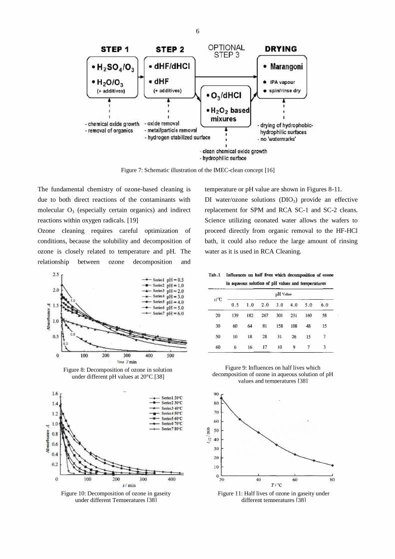
6
Figure 7: Schematic illustration of the IMEC-clean concept [16]
The fundamental chemistry of ozone-based cleaning is
due to both direct reactions of the contaminants with
molecular O3 (especially certain organics) and indirect
reactions within oxygen radicals. [19]
Ozone cleaning requires careful optimization of
conditions, because the solubility and decomposition of
ozone is closely related to temperature and pH. The
relationship between ozone decomposition and
temperature or pH value are shown in Figures 8-11.
DI water/ozone solutions (DIO3) provide an effective
replacement for SPM and RCA SC-1 and SC-2 cleans.
Science utilizing ozonated water allows the wafers to
proceed directly from organic removal to the HF-HCl
bath, it could also reduce the large amount of rinsing
water as it is used in RCA Cleaning.
Figure 8: Decomposition of ozone in solution under different pH values at 20°C [38]
Figure 9: Influences on half lives which decomposition of ozone in aqueous solution of pH
values and temperatures [38]
Figure 10: Decomposition of ozone in gaseity under different Temperatures [38]
Figure 11: Half lives of ozone in gaseity under different temperatures [38]

7
The IMEC cleaning sequence was developed in an effort
to provide a lower cost, less environmentally deleterious,
and in some ways more effective cleaning sequence. [18]
3.3. Supercritical CO2 Cleaning
Supercritical fluids are moieties that exist above their
critical temperature and critical pressure. This has been
considered a fourth state of matter where the material is
neither a liquid nor a gas but has the beneficial properties
of both. In the supercritical state the fluid has the
diffusivity of a gas with the solvency of a liquid and zero
surface tension. These become very desirable properties
for cleaning.[18] The region of supercritical fluids are
illustrated for carbon dioxide in Figure12.
Figure 12: Phase diagram of carbon dioxide
3.1.1. Photo resist removal
The mechanisms for removing photoresist using scCO2
processing differ from a typical wet chemistry approach.
Instead of dissolving the photoresist, the scCO2 can be
used to swell the polymer and then debond it from the
surface, and is lifted off in sheets, as shown in Figure 13.
[18]
Figure 13: Photo resist removal by scCO2 Cleaning
3.1.2. Particle removal
Similar approaches to swell and debond could be used for
organic particle removal. However, for inorganic particles
a different method has been demonstrated. Korzenski et
al. have described the use of chemical additives that
include a combination of etchant, surface passivator and
fluorinated surfactant in scCO2 in order to remove Si3N4
particles from Si or SiO2 surfaces. Particles are removed
by an undercut mechanism whereby the particle/surface
adhesion layer is attacked by the etchant. In order to
minimize the etching of the surface, a passivator is added
[18]. Figure 14 shows particle removal results.
Figure 14: Particle removal results by scCO2 Cleaning
3.4. Wafer rinsing and drying
The last steps in wet-chemical wafer cleaning are rinsing
and drying; both are extremely critical because clean
wafers can become recontaminated very easily. Rinsing
should be done with flowing high-purity and ultra filtered
high-resistivity DI H2O at room temperature. It removes
chemicals between each cleaning step to prevent cross
contamination and at the end of the cleaning sequence to
prevent chemical residues from being left on the wafer.
Wafer drying after rinsing must be done by physical
removal of the H2O, rather than by allowing it to
evaporate, which would leave residues. [18]
3.5. Cleaning tools
In Wet Chemical Cleaning, a bunch of cleaning tools is
used, like single-wafer cleaning tool and wet bench
cleaning tool. This thesis is concentrated in wet bench
Nr.32014-00.
The construction and data of the wet bench which we
need for quantitative risk assessment are demonstrated in
the following Figures.
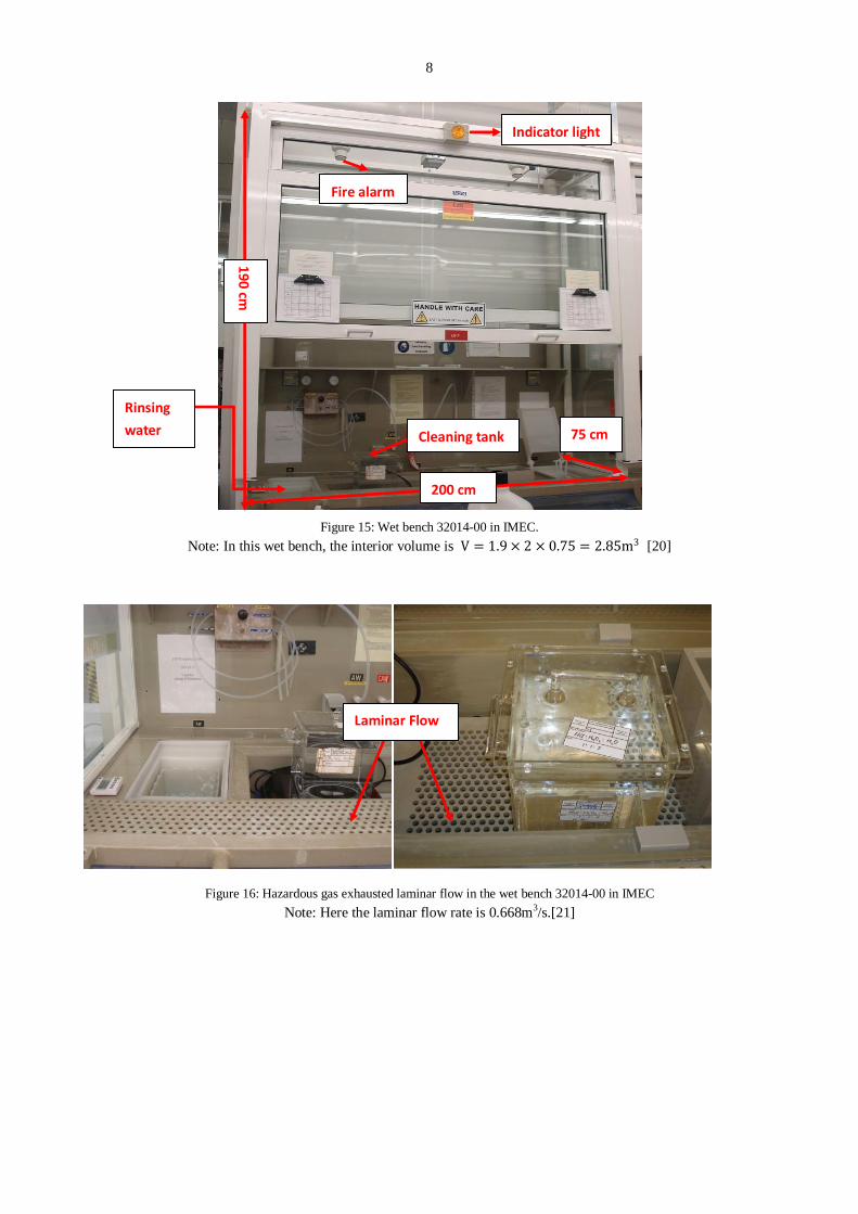
8
Figure 15: Wet bench 32014-00 in IMEC.
Note: In this wet bench, the interior volume is V = 1.9 × 2 × 0.75 = 2.85m3 [20]
Figure 16: Hazardous gas exhausted laminar flow in the wet bench 32014-00 in IMEC
Note: Here the laminar flow rate is 0.668m3/s.[21]
Indicator light
Fire alarm
Rinsing
water Cleaning tank
19
0 cm
200 cm
75 cm
Laminar Flow
9
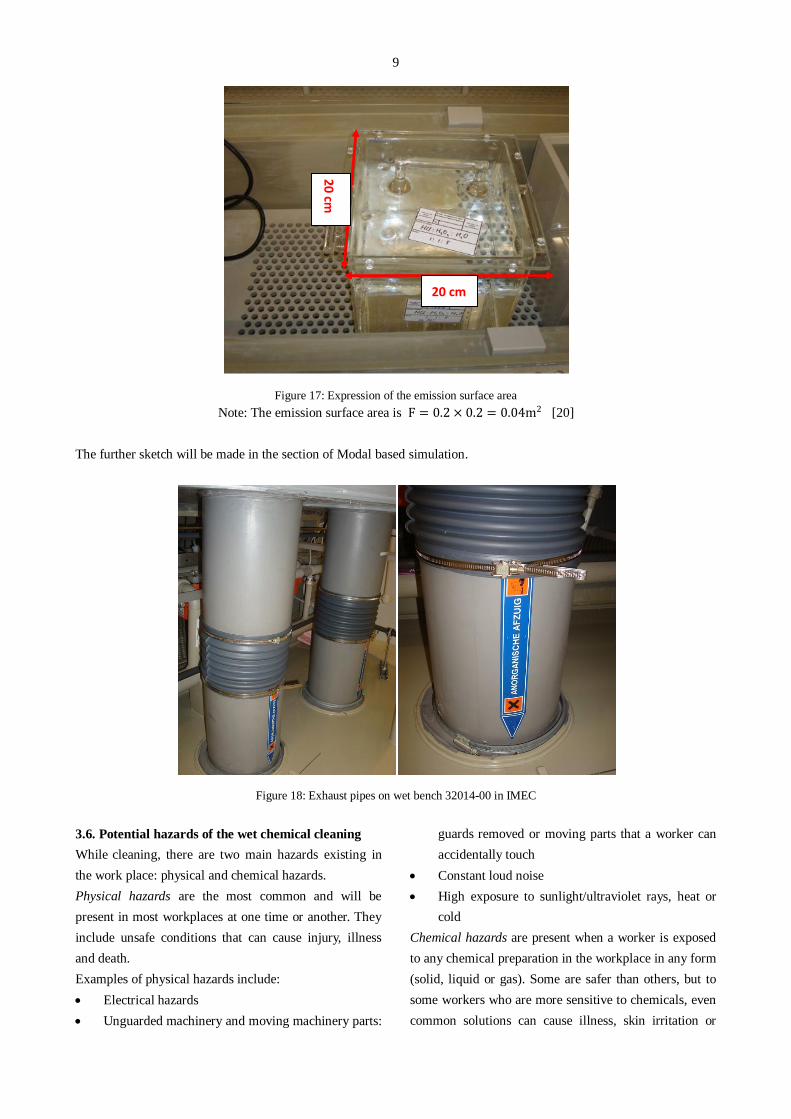
Figure 17: Expression of the emission surface area
Note: The emission surface area is F = 0.2 × 0.2 = 0.04m2 [20]
The further sketch will be made in the section of Modal based simulation.
Figure 18: Exhaust pipes on wet bench 32014-00 in IMEC
3.6. Potential hazards of the wet chemical cleaning
While cleaning, there are two main hazards existing in
the work place: physical and chemical hazards.
Physical hazards are the most common and will be
present in most workplaces at one time or another. They
include unsafe conditions that can cause injury, illness
and death.
Examples of physical hazards include:
Electrical hazards
Unguarded machinery and moving machinery parts:
guards removed or moving parts that a worker can
accidentally touch
Constant loud noise
High exposure to sunlight/ultraviolet rays, heat or
cold
Chemical hazards are present when a worker is exposed
to any chemical preparation in the workplace in any form
(solid, liquid or gas). Some are safer than others, but to
some workers who are more sensitive to chemicals, even
common solutions can cause illness, skin irritation or
20 cm
20
cm

10
breathing problems.
Beware of:
Liquids like cleaning products, paints, acids,
solvents especially chemicals in an unlabelled
container (warning sign!)
Flammable materials like gasoline, solvents and
explosive chemicals.
Vapours and fumes, for instance those that come
from welding or exposure to solvents [22]
The Primary Route(s) of Exposure are:
Skin contact: liquid, mist
Inhalation: vapor, mist
Eye contact: liquid [23]
This paper will concentrate on the acid/alkaline mist and
harmful gases that emit from the solution during the RCA
Cleaning and IMEC Cleaning in the Wet Chemical
Cleaning field. In the next section an exact quantitative
risk assessment is done.
4. Modal based simulation
In order to estimate the exact amount of acidic or alkaline
mist formed above the liquid or the amount of dangerous
gas remaining in the operating environment of the wafer
cleaning bath, especially when there is sufficient air flow
ventilation inside the cleaning tool, a mathematical
simulation model for this dynamic balance problem was
established. In the following paragraphs, the principle of
the model is illustrated for a few typical gases and the
consequent influence of the ambient environment
conditions onto the residue amount is explained.
4.1. Approach
In wet chemical cleaning processes, a variety of acids or
alkalines are often involved for removing the
contaminants on the semiconductor chips. Among those
acids, hydrochloric acid (HCl), hydrofluoric acid (HF),
sulfuric acid (H2SO4) and ammonia solution (NH4OH) are
most commonly used. Except that some physical and
chemical property factors are different for those different
sorts of acid, we could apply similar simulation models in
our calculation for them. Hence, we choose the ammonia
solution as our analysis object and introduced the
establishment of the model according to its properties.
The very first step in establishing the mathematical
simulation model was to get acquainted with the
simulation environment. According to the picture taken
from the wafer cleaning laboratory, a simplified sketch
can be drawn to explain the operating process and the
theoretical approach we can make:
Figure 19: Simplified sketch of the wet bench
As far as we involve the concept of sampling time, this
continuous model has been converted into a discrete
model. Therefore the continuous emission and exhausting
procedure is divided into millions of infinite small
discrete steps. Regarding the initial stage and end stage of
each sub-step, we have their transient concentration as
Xinitial and Xend.
11
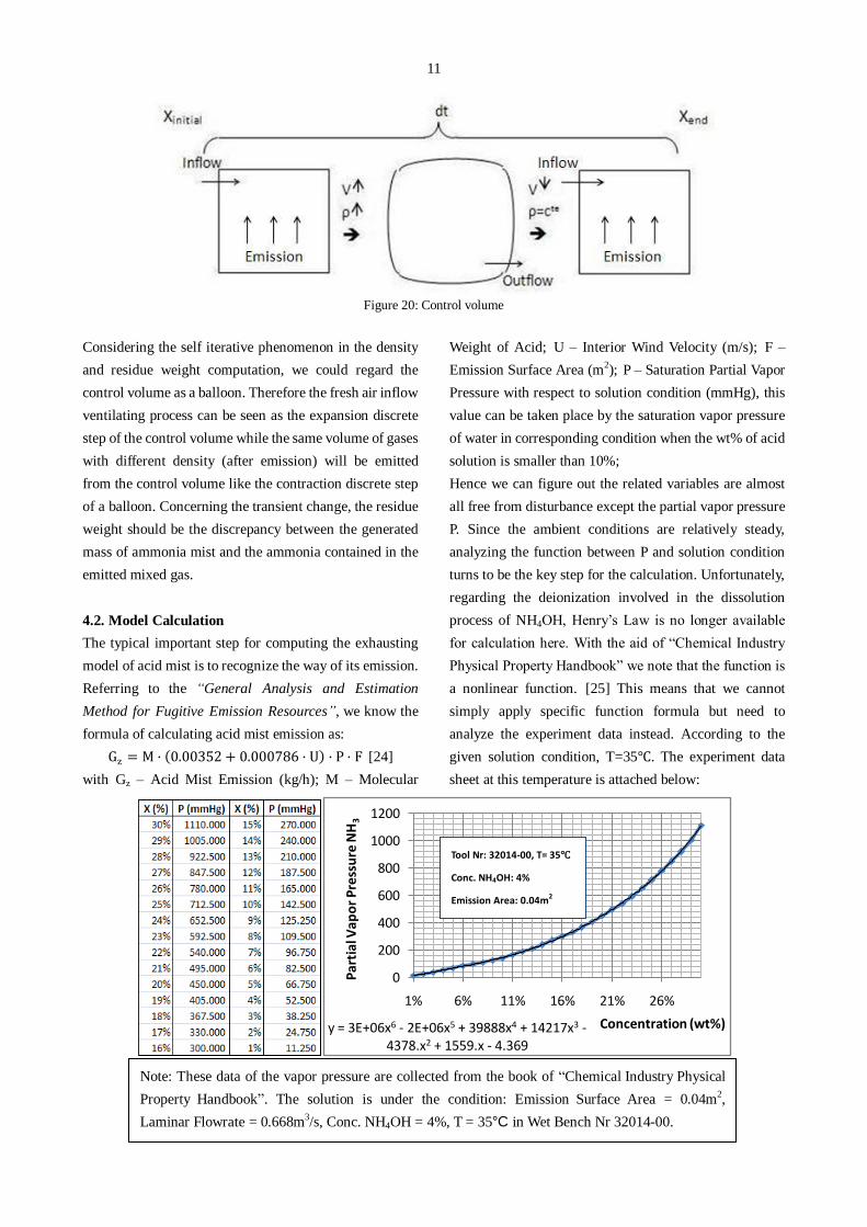
Figure 20: Control volume
Considering the self iterative phenomenon in the density
and residue weight computation, we could regard the
control volume as a balloon. Therefore the fresh air inflow
ventilating process can be seen as the expansion discrete
step of the control volume while the same volume of gases
with different density (after emission) will be emitted
from the control volume like the contraction discrete step
of a balloon. Concerning the transient change, the residue
weight should be the discrepancy between the generated
mass of ammonia mist and the ammonia contained in the
emitted mixed gas.
4.2. Model Calculation
The typical important step for computing the exhausting
model of acid mist is to recognize the way of its emission.
Referring to the “General Analysis and Estimation
Method for Fugitive Emission Resources”, we know the
formula of calculating acid mist emission as:
Gz = M · 0.00352 + 0.000786 ·U ·P ·F [24]
with Gz – Acid Mist Emission (kg/h); M – Molecular
Weight of Acid; U – Interior Wind Velocity (m/s); F –
Emission Surface Area (m2); P – Saturation Partial Vapor
Pressure with respect to solution condition (mmHg), this
value can be taken place by the saturation vapor pressure
of water in corresponding condition when the wt% of acid
solution is smaller than 10%;
Hence we can figure out the related variables are almost
all free from disturbance except the partial vapor pressure
P. Since the ambient conditions are relatively steady,
analyzing the function between P and solution condition
turns to be the key step for the calculation. Unfortunately,
regarding the deionization involved in the dissolution
process of NH4OH, Henry’s Law is no longer available
for calculation here. With the aid of “Chemical Industry
Physical Property Handbook” we note that the function is
a nonlinear function. [25] This means that we cannot
simply apply specific function formula but need to
analyze the experiment data instead. According to the
given solution condition, T=35℃. The experiment data
sheet at this temperature is attached below:
y = 3E+06x6 - 2E+06x5 + 39888x4 + 14217x3 -4378.x2 + 1559.x - 4.369
0
200
400
600
800
1000
1200
1% 6% 11% 16% 21% 26%
Par
tial
Va
po
r P
ress
ure
NH
3
Concentration (wt%)
Note: These data of the vapor pressure are collected from the book of “Chemical Industry Physical
Property Handbook”. The solution is under the condition: Emission Surface Area = 0.04m2,
Laminar Flowrate = 0.668m3/s, Conc. NH4OH = 4%, T = 35°C in Wet Bench Nr 32014-00.
Tool Nr: 32014-00, T= 35℃
Conc. NH4OH: 4%
Emission Area: 0.04m2

12
By ploting the data sheet, we have the graphical relation simulation by the internal Bezier Curve fitting of MS Excel.
Hence the function of this relation can be expressed according to the sextic trendline approximation function equation of
the Bezier Curve:
y = 3E+06x6 - 2E+06x5 + 39888x4 + 14217x3 – 4378.x2 + 1559.x – 4.369
We continue by programming this equation as an internal function model of MS Excel VBA, defining the function as
“VPamm(Conc)” for future calling.
As the saturation partial vapor pressure P is expressed as
the function of solution concentration--VPamm(Conc) in
the same temperature and atmospheric pressure condition,
we can derivate the transfer function from the
concentration of acid solution to the emitted mass of acid
mist as following:
Gz ·dt = M ·(0.00352 + 0.000786 ·U) ·F ·dt
·VPamm(Xinitial )
Xend =msolution ∙ Xinitial − Gzdt
msolution − Gzdt∙ 100%
Xinitial ,n = Xend ,n−1 , Xinitial ,0 = 4%
Here dt stands for the sampling time of discrete steps
which would be taken as a relative small value, for
instance dt=0.1s. Hereby we complete the calculation
concerning the liquid solution, and go way to the
computation of residue acid mist concentration in the
control volume. According to the reference data we take
the air density of 1.2046kg/m3 at 20℃. Then the transient
internal gas density in the control volume after the
expansion discrete step can be computed as:
ρinternal
= V + Qflow ∙ dt ∙ ρ
air+ Gz ∙ dt + mresidue
V + Qflow ∙ dt + (Gz ∙ dt + mresidue ) ρAmmonia
Here Qflow stands for the in and out flow rate of ventilating
air inside the cleaning tool. With this calculated internal
gas density, we can easily calculate the mass of gas at the
transient moment right after the contraction discrete step
(density of gas doesn’t change in emission process).
mair = ρinternal
∙ V
Then we give way to the computation of the ammonia
residue in the current control volume. The value can be
calculated with the aid of the weight percentage of
generated acid mist in control volume gas as:
mresidue ,n = Gz ∙ dt + mresidue ,n−1 − Qflow ∙ dt +
(Gz∙dt+mresidue,n−1)ρAmmonia∙ρinternal∙(Gz∙dt+m
residue,n−1)mair
4.3. Graphical Result Analysis
Till now, the entire mathematical simulation model is
established with input factors and sampling time dt as
variable. Hereby we take the in and out flow rate of
0.668m3/s, sampling time of 0.1 second and inspection
time of 1600dt to see the concentration response of the
residue ammonia as an example.

13
From the graph we can figure out the saturation effect of
the residue concentration. Regarding the theoretical
analysis, this saturation concentration level can be
understood as the dynamic balance level of the in and out
flow. Hence the conclusion should be that the emission
model reaches the dynamic balance stage at
approximately 20s after initial stage and the saturation
residue concentration is around 7.72 ppm.
Reviewing the previous computation steps, we notice that
there is direct link of the saturation residue concentration
with the in and out flow rate inside the cleaning tool. By
changing the variable of flow rate in the mathematical
model, we conclude the relationship as:
0
1
2
3
4
5
6
7
8
9
0 200 400 600 800 1000 1200 1400 1600 1800
Re
sid
ue
Co
nce
ntr
ati
on
(pp
m)
Time (10-1s)
0
10
20
30
40
50
60
0.1 0.3 0.5 0.7 0.9
Co
nce
ntr
atio
n (p
pm
)
Qflow (m3/s)
0.668@IMEC
Tool Nr: 32014-00, T= 35℃
Conc. NH4OH: 4%
Emission Area: 0.04m2
Note: These data of the vapor pressure are collected from the book of “Chemical Industry Physical
Property Handbook”. The solution is under the condition: Emission Surface Area = 0.04m2, Laminar
Flowrate = 0.668m3/s, Conc. NH4OH = 4%, T = 35°C in Wet Bench Nr 32014-00.
Note: These data of the vapor pressure are collected from the book of “Chemical Industry Physical
Property Handbook”. The solution is under the condition: Emission Surface Area = 0.04m2, Laminar
Flowrate = 0.668m3/s, Conc. NH4OH = 4%, T = 35°C in Wet Bench Nr 32014-00.
Tool Nr: 32014-00, T= 35℃
Conc. NH4OH: 4%
Emission Area: 0.04m2

14
Hence as long as the flow rate reaches 0.6m3/s, the
ammonia residue concentration in the interior gas turns to
be smaller than 10ppm. Moreover, each saturation residue
ppm concentration can be looked up from this curve with
corresponding flow rate.
Within the wet bench under investigation a laminar flow
rate of 0.668m3/s has been set. From the curve, the residue
ammonia concentration can be derived to be 7.72 ppm.
The results computed for other acid solutions including
HCl and HF applying similar methodology are contained
in the appendix. Here the saturation residue
concentration for each specific solution is listed in the
table below:
Solution Saturation residue concentration
NH4OH 7.72 ppm
HPM 12.699 ppm
DHCl 3.28*10-4 ppm
HF 6.54*10-3 ppm
4.4. Apply Method for Harmful Gases
Similar to the acid/alkaline mist exhausting model, we
could also establish a discrete mathematical model for the
computation of the emission and residue amount of
dangerous gases generated during the wafer cleaning
processes. Nevertheless, there would of course be some
different formulas involved. Hereby we take the ozonated
water solution as our inspecting object. Notice, an
important upgrade of the simulation system should be
made because of the decomposition phenomenon of
ozone in both air and water environment.
Still according to the “General Analysis and Estimation
Method for Fugitive Emission Resources”, we found the
formula for the harmful gases emission as:
Gs = (5.38 + 4.1 ·U) ·P ·F ·M0.5 [24]
with Gs – Harmful Gas Emission (g/h); M – Molecular
Weight of Acid/Alkaline; U – Interior Wind Velocity
(m/s); F – Evaporation Area (m2); P – Saturation Partial
Vapor Pressure with respect to solution condition (mmHg).
This value would be different from the one of the
ammonia solution model, since the solution is not an
electrolyte solution anymore and the relation of saturation
partial vapor pressure with the ppm concentration of
solution does obey Henry’s Law.
Because of the theoretical linear relationship from
Henry’s Law, we looked up the saturation partial vapor
pressure and ppm concentration of ozonated water at 20℃.
Since the Henry’s Law constant is only relative to the
concentration of ozone in the cleaning solution we
finally use (no matter what % of ozone is generated from
ozone generator), we can gain the following result:
P = 750.2467mmHg; Conc = 368ppm
Therefore the Henry’s Law constant of ozone at T=20℃
can be determined:
KHoz = PConc = 2.038714mmHg/ppm
Regarding the involvement of this constant, the transfer
function from the concentration of the solution to the
emitted mass of dangerous gas can be updated as
following:
Gs ·dt = (5.38 + 4.1 ·U) ·F ·M0.5 ·dt ·KHoz ·Xinitial′
Xend =msolution ∙ Xinitial
′ − Gsdt
msolution − Gsdt∙ 100%
Xinitial ,n′ = Xend ,n−1
′
Another key difference involved here is the difference
between Xinitial′ and Xinitial that we previously used for
the computation of acid mist emission. Considering the
self decomposition half-life of ozone in water solution
with concentration less than 1% and pH value of 7 is
approximately 20 minutes. The sextic trendline
approximation method onto the Bezier Curve can be
applied once again here for the function of decomposition.
The formula below is concluded for the relation
mentioned above:

15
From the simulation, the corresponding internal function of decomposition in water environment should be defined as
OzDW(t) in VBA programming:
This then leads to an easy relation of:
Xinitial′ = Xinitial ∙ OzDW dt
Xinitia ,0′ = 10ppm ∙ OzDW 0.1second
As we continue our computation for the residue ppm
concentration of dangerous gas in the cleaning tool, apart
from the iterative calculation of ρinternal
,
mair and mresidue , the decomposition of ozone in air
should be defined by simulation as well, notice half-life
here is 86 minutes:
y = - 2E-11x3 + 1E-07x2 - 0.000x + 0.998
0%
20%
40%
60%
80%
100%
120%
0 5000 10000 15000
Co
nce
ntr
atio
n (w
t%)
Time (s)
y = - 2E-13x3 + 7E-09x2 - 0.000x + 0.998
0%
20%
40%
60%
80%
100%
120%
0 10000 20000 30000 40000 50000 60000 70000
Co
nce
ntr
atio
n (w
t%)
Time (s)
Tool Nr: 32014-00, T= 20℃
Conc. Ozone: 10ppm
Emission Area: 0.04m2
Tool Nr: 32014-00, T= 20℃
Conc. Ozone: 10ppm
Emission Area: 0.04m2
Note: These data of the vapor pressure are collected from the book of “Chemical Industry Physical
Property Handbook”. The solution is under the condition: Emission Surface Area = 0.04m2,
Laminar Flowrate = 0.668m3/s, Conc. ozone = 10 ppm, T = 35°C in Wet Bench Nr 32014-00.
Note: These data of the vapor pressure are collected from the book of “Chemical Industry Physical
Property Handbook”. The solution is under the condition: Emission Surface Area = 0.04m2, Laminar
Flowrate = 0.668m3/s, Conc. ozone = 10 ppm, T = 35°C in Wet Bench Nr 32014-00.

16
The corresponding internal function of decomposition in water environment should be defined as OzDA(t) in VBA
programming:
The detailed computation procedure is listed below:
ρinternal
= V + Qflow ∙ dt ∙ ρ
air+ Gs ∙ dt + mresidue
V + Qflow ∙ dt + (Gs ∙ dt + mresidue ) ρozone
mair = ρinternal
∙ V
mresidue ,n = Gs ∙ dt + mresidue ,n−1 − Qflow ∙ dt +
(Gs ∙ dt + mresidue ,n−1) ρozone
∙ ρinternal
∙
(Gs ∙ dt+mresidue ,n−1)mair
∙ OzDA dt
Take the in and out flow rate of 0.668m3/s, sampling time
of 0.1 second again and the inspecting time of 1600dt, we
gain the following result graph:
Different from the acid/alkaline mist model, with the
involvement of self decomposition effect of ozone, the
curve shows a fast saturation of 9.92ppm at around T=8s
and then drops down with a decreasing velocity till the
lower limit of 1.87 ppm at around T=150s. Hence as soon
as we stop the emission of ozone from the cleaning
process the concentration drops because of the laminar
outflow.
Similar to the acid/alkaline mist model, we also give the
relationship between the saturation limits and the flow
rate as appendix in convenience for operator to check and
select the proper safe laminar flow rate for the cleaning
process.
0
2
4
6
8
10
12
0 200 400 600 800 1000 1200 1400 1600 1800
Ozo
ne
Res
idu
e C
on
cen
tra
tio
n (p
pm
)
Time (10-1s)
Tool Nr: 32014-00, T= 20℃
Conc. Ozone: 10ppm
Emission Area: 0.04m2
Note: These data of the vapor pressure are collected from the book of “Chemical Industry Physical
Property Handbook”. The solution is under the condition: Emission Surface Area = 0.04m2, Laminar
Flowrate = 0.668m3/s, Conc. ozone = 10 ppm, T = 35°C in Wet Bench Nr 32014-00.
17
In the wet bench under investigation the laminar flow rate
is 0.668m3/s. From the graph we can see that the
maximum residual ozone concentration is reached after 8s
(9.92 ppm) and the final residue ozone concentration is
1.87 ppm after 150s.
5. Health Effects and Relative Limits
5.1. Definition of Common Terms
ACGIH = American Conference of Governmental
Industrial Hygienists
ATSDR = Agency for Toxic Substances and Disease
Registry
NAAQS = National Ambient Air Quality Standards
EPA = Environmental Protection Agency
TLV = Threshold Limit Value (guidelines to assist in the
control of occupational health hazards)
TWA = Time-Weighted Average (8 hours)
STEL = Short-Term Exposure Limit (15 minutes)
5.2. Ammonia
Ammonia, in both its gaseous and liquid form, can be
irritating to the eyes, respiratory tract and skin due to its
alkaline nature. The biological effects of ammonia in
humans after acute exposures are dose-related – they
depend on the ambient concentration, the amount taken in
by the body and the duration of exposure.
ACGIH recommends a threshold limit value (TLV) of 35
ppm as a short-term exposure limit (STEL) and 25 ppm on
a time weighted average (TWA) to avoid irritation of the
eyes, nose and throat. The other effects due to the
different concentration of ammonia have been illustrated
in table 2. [26]
A study conducted on workers exposed to ammonia for 10
to 15 years at levels up to and exceeding 24 ppm did not
find adverse effects. In additional occupational studies, no
relationship was found between exposure to ammonia and
cancer or carcinogenicity. [26]
According to the ATSDR studies, chronic exposure to
ammonia (under 25 ppm) did not result in harm to genetic
material or damage the reproductive system or a
developing fetus.
05
10152025303540
0.1 0.3 0.5 0.7 0.9
Co
nce
ntr
atio
n (p
pm
)Qflow (m
3/s)
Cmin
Cmax
0.668@IMEC
Tool Nr: 32014-00, T= 20℃
Conc. Ozone: 10ppm
Emission Area: 0.04m2
Note: These data of the vapor pressure are collected from the book of “Chemical Industry Physical
Property Handbook”. The solution is under the condition: Emission Surface Area = 0.04m2,
Laminar Flowrate = 0.668m3/s, Conc. ozone = 10 ppm, T = 35°C in Wet Bench Nr 32014-00.
18
Concentration / Time Health Effect
10,000 ppm Promptly lethal
5,000 – 10,000 ppm Rapidly fatal
700 – 1700 ppm Incapacitation from tearing of the eyes and coughing
500 ppm for 30 minutes Upper respiratory tract irritation, tearing of the eyes
134 ppm for 5 minutes Tearing of the eyes, eye irritation, nasal irritation, throat irritation, chest
irritation
140 ppm for 2 hours Severe irritation, need to leave exposure area
100 ppm for 2 hours Nuisance eye and throat irritation
50 – 80 ppm for 2 hours Perceptible eye and throat irritation
20 – 50 ppm (TLV-TWA=25
ppm)
Prolonged repeated exposure produces no injury
Table 2: Concentration/Duration/Effect of NH3 vapor (without protective clothing) [26]
5.3. Hydrochloric acid
Hydrochloric acid is corrosive to the eyes, skin, and
mucous membranes. Acute inhalation exposure may
cause coughing, hoarseness, inflammation and ulceration
of the respiratory tract, chest pain, and pulmonary edema
in humans. [27-29]
Pulmonary irritation, lesions of the upper respiratory tract,
and laryngeal and pulmonary edema have been reported
in rodents acutely exposed by inhalation. [27-29]
Brief exposures (up to a few minutes) to concentrations in
the range of 1,300 to 2,000 ppm are lethal to humans [30].
In workers, exposure to 50 to 100 ppm for 1 hour was
barely tolerable; short exposure to 35 ppm caused
irritation of the throat. In one study, workers chronically
exposed to hydrogen chloride did not exhibit the
pulmonary function changes observed in nine subjects
exposed to similar concentrations, which suggests that
workers become acclimatized to hydrogen chloride [31].
Dental discoloration and erosion of exposed incisors may
occur on prolonged exposure to low concentrations [32].
More effects according to different concentration of
hydrochloric acid are indicated in Table 3:
Exposure Health Effects
5 ppm (TLV-TWA) No health effects are expected.
10 ppm Does not interfere with work
10 ppm mice 90 days Mild rhinitis
> 10 ppm Acute local irritation among acclimatized workers
30 ppm, 1 hr no clinical manifestation
30 ppm upper limit of safety
30 ppm mice 90 days eosinophilic globules in nasal turbinate epithelial tissue
35 ppm irritation of throat for short exposure
50 - 100 ppm barely tolerable
Table 3: Relative limits of HCl vapor [33]
5.4. Hydrogen fluoride
In humans, inhalation of hydrogen fluoride gas may cause
immediate or delayed-onset pulmonary edema after a
1-hour exposure [31]. Repeated exposure to excessive
concentrations of fluoride over a period of years results in
increased density of bone and eventually may cause
crippling fluorosis (osteosclerosis caused by the
deposition of fluoride in bone) [31]. Ingestion of an
estimated 1.5 grams of hydrofluoric acid produces sudden
death; however, repeated ingestion of small amounts of
hydrogen fluoride may cause fluoride osteosclerosis. [34]
The relative limits are indicated in Table 4:

19
Exposure Health Effects
3 ppm (TLV-TWA) Has a strong irritation odor, does not interfere with work over an 8-hour work day
10 to 15 ppm irritate the eyes, skin, and respiratory tract
30 ppm Respiratory symptoms worsen. Can be tolerated for several minutes
50 ppm May be fetal if inhaled for 30-60 minutes
120 ppm Maximum concentration in air that can be tolerated for 1 minute. Smarting of the skin,
conjunctivitis and irritation of the respiratory tract occur
Table 4: Relative limits of HF vapor [35]
5.5. Ozone
The human health effects of ozone have been studied for
over 30 years. The respiratory system is the primary target
of this oxidant pollutant. The degree of adverse
respiratory effects produced by ozone depends on several
factors, including concentration and duration of exposure,
climate characteristics, individual sensitivity, preexistent
respiratory disease, and socioeconomic status [36].
The United States Environmental Protection Agency
(EPA) has classified ozone as a criteria pollutant. EPA
has established National Ambient Air Quality Standards
(NAAQS) of 0.12 parts per million (ppm) averaged over 1
hour (not to be exceeded more than three times in a
3-years period), and 0.08 ppm averaged over 8 hour.
However, recent epidemiological studies have shown that
1-hour ozone levels lower than 0.12 ppm and 8-hour
levels lower than 0.08 ppm produce adverse health effects
in the general population. [37] The relative limits are
indicated in Table 5.
8-hour average ozone
Concentration (ppm)
Air Quality Descriptor Health Effects
0.0 to 0.064 Good No health effects are expected.
0.065 to 0.084 Moderate Usually sensitive individuals may experience
respiratory effects from prolonged outdoor exertion
if you are unusually sensitive to ozone.
0.085 to 0.104 Unhealthy for Sensitive
Groups
Member of sensitive group may experience
respiratory symptoms (coughing, pains when taking
a deep breath).
0.105 to 0.124 Unhealthy Member of sensitive group have higher chance of
experiencing respiratory symptoms (aggravated
cough or pain), and reduces lung function.
0.125 (8-hr) to 0.404 (1-hr) Very Unhealthy Members of sensitive groups experience
increasingly severe respiratory symptoms and
impaired breathing.
0.25-0.75 ppm Very Unhealthy Cause cough, shortness of breath, tightness of the
chest, a feeling of an inability to breathe (dyspnea),
dry throat, wheezing, headache and nausea.
Table 5: Relative limits of ozone [37]

20
Conclusion
Regarding the standard laminar flow rate of 0.668m3/s
used in the wafer cleaning process, we can analyze our
calculation result based on economic consideration. For
the two types of hydrochloric acid we often used: HPM
(1:1:5, 80°C), DHCl (1:1000, 20°C), the saturation
residue concentration are correspondingly 12.699 ppm
and 3.28*10-4 ppm. And for Hydrogen chloride, the
safety limit is 5 ppm. Hence we can figure out for HPM,
the residue is higher than the safety limit (5 ppm), but
after the emission of acid fog halts (put the lid on), the
residue concentration would drop to the safety level
within 4 second. For DHCl the residue is 3.28*10-4 ppm,
we got already relative low ppm concentration, it is even
too low that our flow rate is set extra too high for
controlling DHCl emission.
For hydrofluoric acid, we got similar result as DHCl. The
saturation residue concentration turns to be as low as
6.54*10-3 ppm, and is far lower than the safety limit 3
ppm, which still indicates the waste of high laminar flow
rate.
For ammonia solution, we notice the saturation residue
concentration is 7.72 ppm, which is much lower than the
safety requirement 25 ppm. Therefore considering
economic reasons, we can even reduce the laminar flow
rate to 0.25 m3/s for this specific application to gain a safe
result (20.84 ppm at 0.25m3/s).
For the application in ozonated water, the maximum
saturation residue is 9.92ppm at around T=8s and then
drops down with a decreasing velocity till the lower limit
of 1.87 ppm at around T=150s, and again above the safety
limit (0.06 ppm). So we can still check the curve after we
stop the emission of dangerous gas (put the lid on) and
find out that within 13 seconds the concentration would
become lower than 0.06 ppm.
0
2
4
6
8
10
12
14
0 500 1000 1500 2000
HC
l Res
idu
e C
on
cen
tra
tio
n (p
pm
)
Time (10-1s)
1600
1640(10-1
s)
21
Acknowledgements
The author expresses his gratitude to co-promoters Alain
Pardon and Nausikaä Van Hoornick, IMEC, Belgium and
her promoter Patrick Lievens, GroepT Leuven Belgium
for comprehensive instruction.
Special thank should also be given to Kathleen
Verbraeken, Rita Vos, Jan Coenen, Miel Sledsens and Els
Vanlee from IMEC for their effort and help during the
research stage of this thesis project.
Reference
[1] http://www.mkaq.org/anquanpj/pingjiaal/200905/anquanpj_11236.html
[2] http://en.wikipedia.org/wiki/Hazard
[3] http://www.ccohs.ca/oshanswers/hsprograms/hazard_risk.html
[4] http://en.wikipedia.org/wiki/Semiconductor_device_fabrication
[5] Delfi, IMEC learning site.
[6] Luc Arkens, Judith Staginus, “Process risk assessment of semiconductor layering techniques”, master thesis, Groep T,
Leuven, 2007
[7] Peter Van Zant, “Microchip Fabrication: A Practical Guide to Semiconductor Processing”, 5th ed, Printed and bound
by R. R. Donnelley, 2004, ISBN 0-07-143241-8.
[8] http://python.rice.edu/~arb/Courses/Images/360_02_handout9.jpg
[9] http://141.223.168.19/process.html
[10] http://en.wikipedia.org/wiki/Photolithography
[11] http://www.photochembgsu.com/applications/photoresists.html
[12] Prof, Tayo Akinwande, Lecture 13: “Wet Etching, Etching and Pattern Transfer (1)”, Fall Term 2003
[13] Shuo Wang “Process risk assessment of semiconductor Doping techniques”, master thesis, Groep T, Leuven, 2008.
[14] http://www.iue.tuwien.ac.at/phd/wittmann/node7.html
[15] http://www.gs68.de/tutorials/implant.pdf
[16] Wolf, Stanley, “Microchip Manufacturing” 2004, ISBN 0-9616721-8-8
[17] http://www.glsciences.com/products/application-specificInstruments/swa256_series.html
[18] Karen A. Reinhardt, Werner Kern, “Hand book of silicon wafer cleaning technology”, 2nd ed, USA, 2007, ISBN
978-0-8155-1554-8 (978-0-8155)
0
2
4
6
8
10
12
0 500 1000 1500 2000
Re
sid
ue
Co
nce
ntr
ati
on
(pp
m)
Time (10-1s)
1600 1732

22
[19] http://www.mksinst.com/docs/UR/40330-375.pdf, Clean Rooms, Jan 2005
[20] By measurement in the lab
[21] Personal communication with IMEC employer.
[22] http://www.worksmartontario.gov.on.ca/scripts/default.asp?contentID=2-6-1&mcategory=health
[23] James Unmack, MS, CIH and Michael Kleinman, PhD, “Darft Hydrogen Chloride Health-Based Assessment and
Recommendation for HEAC”, January 29, 2008
[24] Yajun Li, “General Analysis and Estimation Method for Fugitive Emission Resources”, October, 2005
[25] Guangqi Liu, Lianxiang Ma, and Zhiyou Xing, “Chemical Industry Physical Property Handbook”, China, 2002,
ISBN 7-5025-3593-4.
[26] http://www.tfi.org/publications/HealthAmmoniaFINAL.pdf
[27] U.S. Department of Health and Human Services. Hazardous Substances Data Bank (HSDB, online database).
National Toxicology Information Program, National Library of Medicine, Bethesda, MD. 1993.
[28] M. Sittig. “Handbook of Toxic and Hazardous Chemicals and Carcinogens”. 2nd ed. Noyes Publications, Park Ridge,
NJ. 1985.
[29] “The Merck Index. An Encyclopedia of Chemicals, Drugs, and Biologicals”. 11th ed. Ed. S. Budavari. Merck and Co.
Inc., Rahway, NJ. 1989.
[30] Braker W, Mossman AL. “Matheson gas data book”. 6th ed. Secaucus, NJ: Matheson Gas Products, Inc, 1980.
[31] Hathaway GJ, “Chemical hazards of the workplace”. 3rd ed, Proctor NH, Hughes JP, and Fischman ML, New York,
NY: Van Nostrand Reinhold, 1991.
[32] Sittig M. “Handbook of toxic and hazardous chemicals”. 3rd ed. Park Ridge, NJ: Noyes Publications, 1991.
[33] http://www.osha.gov/SLTC/healthguidelines/hydrogenchloride/recognition.html
[34] Gosselin RE, Smith RP, Hodge HC, “Clinical toxicology of commercial products”. 5th ed. Baltimore, MD: Williams
& Wilkins, 1984.
[35] http://www.osha.gov/SLTC/healthguidelines/hydrogenfluoride/recognition.html
[36] White, M.C.. “Exacerbations of childhood asthma and ozone pollution in Atlanta. Environmental Research”. 65:
56-58, 1994.
[37] Marian Fierro, “Ozone Health Effects”, First revision (JB) 12/23/99.
[38] Tan Guixia,Chen Yepu,Xu Xiaoping, “Ozone Decomposition Rules in Gaseity and Aqueous Solution”, School of
Sciences,Shanghai University, China, 2004.
Related Documents