1 Process Optimization for Lattice-Selective Wet Etching of Crystalline Silicon Structures Ronald G. Dixson National Institute of Standards and Technology, 100 Bureau Drive Gaithersburg, MD 20899-8212 Phone number: 301-975-4399 Fax: 301-869-0822 Email: [email protected] William F. Guthrie National Institute of Standards and Technology, 100 Bureau Drive Gaithersburg, MD 20899-8980 Phone number: 301-975-2854 Fax: N/A Email: [email protected] Richard A. Allen National Institute of Standards and Technology, 100 Bureau Drive Gaithersburg, MD 20899-8120 Phone number: 301-975-5026 Fax: 301-869-0822 Email: [email protected] Ndubuisi G. Orji National Institute of Standards and Technology, 100 Bureau Drive Gaithersburg, MD 20899-8212

Welcome message from author
This document is posted to help you gain knowledge. Please leave a comment to let me know what you think about it! Share it to your friends and learn new things together.
Transcript

1
Process Optimization for Lattice-Selective Wet Etching of Crystalline Silicon Structures
Ronald G. Dixson
National Institute of Standards and Technology, 100 Bureau Drive Gaithersburg, MD 20899-8212
Phone number: 301-975-4399
Fax: 301-869-0822
Email: [email protected]
William F. Guthrie
National Institute of Standards and Technology, 100 Bureau Drive Gaithersburg, MD 20899-8980
Phone number: 301-975-2854
Fax: N/A
Email: [email protected]
Richard A. Allen
National Institute of Standards and Technology, 100 Bureau Drive Gaithersburg, MD 20899-8120
Phone number: 301-975-5026
Fax: 301-869-0822
Email: [email protected]
Ndubuisi G. Orji
National Institute of Standards and Technology, 100 Bureau Drive Gaithersburg, MD 20899-8212

2
Phone number: 301-975-3475
Fax: 301-869-8022
Email: [email protected]
Michael W. Cresswell*
National Institute of Standards and Technology, 100 Bureau Drive Gaithersburg, MD 20899-8120
Phone number: N/A
Fax: N/A
Email: [email protected]
Christine E. Murabito*
National Institute of Standards and Technology, 100 Bureau Drive Gaithersburg, MD 20899-8120
Phone number: N/A
Fax: N/A
Email: [email protected]
*Present addresses unavailable. (Authors were with NIST during their involvement with this work,
but are no longer affiliated with NIST.)

3
ABSTRACT
Lattice-selective etching of silicon is used in a number of applications, but it is particularly
valuable in those for which the lattice-defined sidewall angle can be beneficial to the functional
goals. A relatively small but important niche application is the fabrication of tip characterization
standards for critical dimension atomic force microscopes (CD-AFMs).
CD-AFMs are commonly used as reference tools for linewidth metrology in semiconductor
manufacturing. Accurate linewidth metrology using CD-AFM, however, is critically dependent
upon calibration of the tip width. Two national metrology institutes (NMIs) and at least two
commercial vendors have explored the development of tip calibration standards using lattice-
selective etching of crystalline silicon.
The National Institute of Standards and Technology (NIST) standard of this type is called
the single crystal critical dimension reference material (SCCDRM). These specimens, which are
fabricated using a lattice-plane-selective etch on (110) silicon, exhibit near vertical sidewalls and
high uniformity and can be used to calibrate CD-AFM tip width to a standard uncertainty of less
than 1 nm.
During the different generations of this project, we evaluated variations of the starting
material and process conditions. Some of our starting materials required a large etch bias to achieve
the desired linewidths. During the optimization experiment described in this paper, we found that
for KOH etching of the silicon features, it was possible to independently tune the target linewidth
and minimize the linewidth non-uniformity. Consequently, this process is particularly well-suited
for small-batch fabrication of CD-AFM linewidth standards.

4
Keywords: lattice-selective etching, crystalline silicon etching, CD-AFM, metrology, CD,
linewidth, SCCDRM, standards, calibration
5
1. INTRODUCTION
Anisotropic, lattice-selective etching of silicon has been known and used in semiconductor
manufacturing since the 1960s.[1] It has been used for a number of applications, but it is
particularly valuable in those for which the lattice-defined sidewall angle can be beneficial to the
functional goals.[2-5] The potential for deep etching of near-vertical sidewalls has also made it
appropriate for micro-electromechanical systems (MEMS).[6-9] During the last 15 years a
relatively small but important niche application in metrology has emerged: the fabrication of tip
characterization standards for critical dimension atomic force microscopes (CD-AFMs).[10-13]
CD-AFMs use flared tips and two-axis surface sensing and tip control in order to image
features with vertical and slightly reentrant sidewalls.[14-15] These instruments are commonly
used as reference tools for linewidth metrology in semiconductor manufacturing. Accurate
linewidth metrology using CD-AFM, however, is critically dependent upon calibration of the tip
width.[16-17] Since the primary effect of CD-AFM tip-sample dilation is an additive bias of the
measured width, the most effective method of tip calibration is to measure the apparent width of a
known structure to determine the effective tip width.
Historically, many CD-AFM users have developed in-house reference standards for tip
width calibration – often based on scanning electron microscope (SEM) or transmission electron
microscope (TEM) cross sections. But the resultant uncertainty of such standards can be
significant. Tip characterizer samples - which have a sharp ridge that can be used to calibrate tip
width - are commercially available. However, scanning such samples can result in tip damage, and
the standard uncertainty of tip calibrations based on this typically exceeds 5 nm.
Since the early 2000s, two national metrology institutes (NMIs), the National Institute of
Standards and Technology (NIST) in the United States and the Physikalisch-Technische

6
Bundesanstalt (PTB) in Germany, and at least two commercial vendors have explored the
development of standards suitable for CD-AFM tip calibration.[10-13,18] In most of these cases,
lattice-selective etching of crystalline silicon was involved in the fabrication process.
The NIST standard of this type is called the single crystal critical dimension reference
material (SCCDRM). These specimens, which are fabricated using a lattice-plane-selective wet etch
on (110) silicon, exhibit near vertical sidewalls and high uniformity and can be used to calibrate
CD-AFM tip width to a standard uncertainty of less than 1 nm.
During the different generations of this project, we experimented with different variations on
the starting material and process conditions – including the etchant.[11,19] Both potassium
hydroxide (KOH) and tetramethyl ammonium hydroxide (TMAH) are commonly used etchants.
Some of our starting materials required a large etch bias to achieve the desired linewidths. During
the optimization experiment described in this paper, we found that for KOH etching of the silicon
features, it was possible to independently tune the target linewidth and minimize the linewidth non-
uniformity. Consequently, this process is particularly well-suited for small-batch fabrication of
CD-AFM tip calibration standards.
2. SCCDRM ETCH PROCESS OPTIMIZATION EXPERIMENT
The background and overall methodology of the SCCDRM project has been described
elsewhere.[10-11] While we have experimented with differences in the starting material and
processing, the use of selective etching on (110) Si has always been a key element. For some
generations of the project, we used starting material with a buried oxide that served both as an etch
stop and as an electrical isolation layer. In this paper, we are specifically dealing with etch

7
optimization experiments using silicon-on-insulator (SOI) starting material that itself was fabricated
using an implantation process – such as separation by implantation of oxygen (SIMOX).
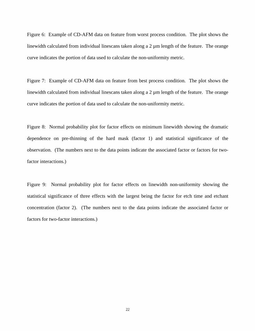
In figure 1, we illustrate some of the major characteristics of the current starting material
and process. The substrate and device layer – in which the features are patterned – are both (110)
crystalline silicon and are separated by a buried oxide. The device layer was approximately 160 nm
thick and the buried oxide was about 390 nm. This same type of starting material was also used in
prior generations of the SCCDRM [11,19] – including the first one to combine the use of CD-AFM
and HRTEM for the calibration.[10]
For small-batch fabrication projects like the SCCDRMs, access to suitable lithography at
affordable costs can be a challenge. The trade-offs between electron beam direct write lithography
and optical lithography present challenges either way. Electron beam lithography offers very small
resolution, avoids the cost of mask making, and does not require large batches or even whole
wafers. However, the cost is generally proportional to write time and thus essentially proportional
to the patterned area. This makes it most suitable for samples on which the patterned region is a
relatively small percentage of the surface area.
Optical lithography, on the other hand has much higher throughput and lower cost for
patterned area, but significantly worse resolution and a large one-time cost of mask fabrication. The
minimum sensible batch size would correspond to a whole wafer – with those associated costs. For
applications in which the lithography resolution is not a limiting factor (e.g., when an etch bias can
be used to achieve the desired feature width) and the mask costs are affordable, the advantages of
optical lithography probably outweigh those of electron beam lithography. Ultimately, we used
i-line (365 nm) lithography for most generations of the SCCDRMs and for the starting material used
in this etch optimization experiment.

8
The typical hard mask thickness is about 10 nm. In some of our earlier experiments, a
silicon nitride hard mask was used because nitride has greater resistance to the selective etch step.
However, the post etch removal of a nitride mask is significantly more difficult than the removal of
an oxide. In some prior experiments, particles or residue from the hard mask remained on the final
features. Therefore, we used an oxide hard mask for SCCDRM production and for the current
optimization experiment.
Following the lithography and pattern transfer to the hard mask, the wafers were diced into
individual chips for the remainder of the process. A lattice-plane-selective etch is then used to
define the features in the device layer. During some generations of this project, both tetramethyl
ammonium hydroxide (TMAH) and potassium hydroxide (KOH) were evaluated as etchants.
For previous production generations of SCCDRMs, the etchant used was TMAH.[11,19]
This was motivated largely by the use of an oxide hard mask which has a greater resistance to
TMAH than to KOH. For the current process optimization experiment, however, we used a KOH
etch – which has a larger relative lattice-plane selectivity than TMAH and offers the potential for a
greater etch bias.
2.1 Design of Etch Optimization Experiment
The final feature characteristics of the SCCDRM will have some dependence on both the
properties of the starting material and performance of the lithography. However, it is the lattice-
selective etch that is central to functional application of the features. Since the wafers were diced
into individual chips after the lithography, it is also possible to readily vary the etch parameters on a
chip by chip basis. More importantly, our overall technical objectives were to reduce feature size
and CD non-uniformity, and we believe that these characteristics have a greater sensitivity to the

9
etch conditions than to the details of the initial lithography. The etch-related factors were thus the
focus for this optimization experiment.
Barring major defects in crystallinity of the device layer or on the mask pattern, we would
expect the selective etch to smooth out most of the width non-uniformity of the features due to
imperfections in the mask or the lithography step. But the extent to which this is accomplished will
depend on how closely the etch conditions correspond to an idealized model. In addition to the
primary etch conditions, we also incorporated cleaning factors into the experiment. Although the
cleaning process is not the central issue in fabrication of SCCDRMs, the removal of both
particulates and hydro-carbon deposition from scanning electron microscope (SEM) inspection
were of concern during the project.
The overall process optimization experiment employed a model with six two-level factors in
a 26-2 or quarter-replicate design. This method allows for estimation of all main effects and some
two-factor interactions from only 16 runs instead of the 64 that would be required in a full factorial
design.[20]
The six factors were:
1. Pre-thinning of the oxide hard mask before silicon patterning,
2. Concentration of KOH and etch duration used for patterning,
3. Use of ultrasonic agitation during patterning,
4. Use of ultrasonic agitation during cleaning of chips with iso-propyl alcohol,
5. Duration of cleaning with iso-propyl alcohol, and
6. Use of acetone or acetone and gaseous ozone to remove carbon deposits following
SEM inspection.
10
The inclusion of a post-SEM cleaning step as factor 6 served to support the goals of using
SEM inspection on the SCCDRMs during process development. The observed effects of factor 6
would allow us to evaluate the performance of the SCCDRMs under SEM inspection and the
consequent importance of the cleaning process for potential contamination. However, our emphasis
here is on the application of SCCDRMs for CD-AFM tip calibration. Since SEM inspection and
cleaning is not required for this purpose, most of our analysis and discussion will be limited to the
first five factors. As shown in table I, this scope reduction results in a model with five two-level
factors in a 25-1 or half-replicate design.
The process flow generally follows the order of the factors above and from left to right
across the columns in table I. However, factors 2 and 3 pertain to the same process step – the
lattice-selective silicon etch – and thus occur simultaneously. This is also true of factors 4 and 5 –
which describe the cleaning step after patterning. Note also that factor 1 has a complementary
process step – the hard mask strip – which is shown in table I, but which is not treated as an
independent factor. This is because the total etch time using the buffered oxide etch (BOE) is held
constant at 18 seconds – which was determined to be sufficient to remove all of the oxide.
Therefore, the variable described by factor 1 indicates whether the oxide mask is stripped in one
step following the lattice-selective silicon etch, or in two steps including a pre-thinning.
Optical inspection, when necessary to verify chip condition, was performed on the chips
during the process steps involving the first five factors. At that point, CD-AFM measurements were
performed to determine the linewidth and non-uniformity of the target features. Then an SEM
inspection was performed and the final cleaning step (factor 6) was completed. The CD-AFM
measurements were performed at NIST, but the SEM measurements were performed by an external
supplier.
11
The SCCDRM chips have a large number of features on them, and the measurement of all of
them by either AFM or SEM would be prohibitive. For this experiment we focused on the variable
linewidth grid (VLG) targets. Each VLG target consists of an array of six lines of different
designed linewidths. A top-down SEM image of a VLG target is shown in figure 2, and a CD-AFM
image of a VLG target is shown in figure 3. Note that the orientation of the target differs by 90º
between the images since CD-AFM data is typically rendered with the horizontal image axis
corresponding to the fast scan axis. This type of target has both processing and metrology benefits.
For processing purposes, this design provided a means of checking how the measured and designed
widths tracked locally independent of spatial variations in etching or material. For metrology
purposes, these targets allowed the incorporation of a scale linearity test into the CD-AFM tip width
calibration. The VLG targets are also referred to as high resolution transmission electron
microscopy (HRTEM) targets, because they were used for both the HRTEM transfer and the final
calibration steps using CD-AFM.[10]
For the first phase of AFM measurements, which was performed after the process steps
corresponding to the first five factors, we selected two types of target on each chip. One was the
smallest design-width target that had all six features intact, and was, in general, different for every
chip. This choice was necessary to assess the factor effects on minimum linewidth. The second
target measured on each chip was one with the largest design-width – which was always the same.
This choice would potentially allow us to detect any influence related to defects in the mask, and it
also provides independent confirmation of the factor effects on non-uniformity determined from the
measurements of the smallest design-width targets.
Following the first phase of AFM measurements, the SEM measurements were performed
only on the smallest surviving design-width targets. An AFM re-check of selected targets was then

12
performed to assess the level of hydrocarbon contamination deposited by the SEM. A typical level
of contamination is a few nanometers thick.
The last cleaning step, described by factor 6, was used to remove any contamination
deposited during the SEM inspection. Although alternative cleaning processes may be explored in
the future, we decided to compare an acetone clean with an acetone and ozone clean for this factor.
Following the final clean, those features that had been measured by SEM were measured again
using the AFM.
2.2 Analysis of Results
We analyzed the CD-AFM data to determine the sensitivity of two feature characteristics to
the experimental factors. These characteristics were the minimum linewidth and linewidth non-
uniformity. To quantify the non-uniformity, we used a metric that was developed as part of our
uncertainty analysis for using CD-AFM to transfer the HRTEM calibration to other samples.
Essentially, this metric involves the use of a triangular weighting function over the central 0.5 µm
of the AFM data set – or 20 line scans – to calculate an average and standard uncertainty of the
linewidth in that region. (Note that in figure 3, this region corresponds to 25 % of the image
centered on the ‘tip’ of the navigation marker that is visible to the side.) This choice was motivated
by our treatment of TEM/AFM relative positioning uncertainty when using CD-AFM in concert
with HRTEM, and the details have been previously published.[10-11]
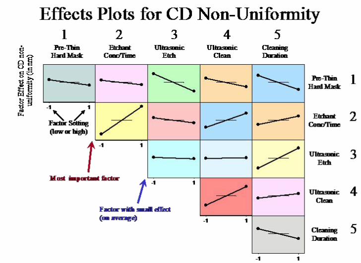
In figures 4 and 5 the factor effects plots for minimum linewidth and non-uniformity are
shown. Only the effects of the first five factors are included in these plots, because these results
were calculated from the initial AFM measurements (i.e., pre-SEM) taken on the smallest surviving
target on each chip. We note, however, that the results taken from the largest design width target on

13
each chip lead to a substantively similar conclusion. This means that, as expected, there is no
significant dependence on the specific target selected.
As the factor effects plots reveal, the minimum linewidth that survived etching is sensitive
primarily to pre-thinning the hard mask and has little dependence on the remaining factors. This is
physically reasonable since the narrowest features will be quickly undercut during oxide etch which
strips the hard mask. Consequently, removing as much hard mask as possible up front can be
expected to increase the survival of narrow lines. Additionally, it must be remembered that the hard
mask is not totally immune to the KOH etch. The etch rate of the silicon is expected to be two to
three orders of magnitude larger than the etch rate of the oxide hard mask. However, we did not
experimentally verify this. And it is possible that once the hard mask is sufficiently pre-thinned, the
effective lateral etch rate of the KOH on the oxide is sufficient to decrease the ultimate width of the
resultant features. This also favors narrow lines and is consistent with our observations.
The non-uniformity has sensitivity to several factors and two-factor interactions, but very
little sensitivity to pre-thinning of the hard mask. However, the single largest sensitivity is to the
etchant concentration and etch time factor. This is also physically reasonable since we believe that
local variations in the etch environment (e.g. concentration gradients) are a significant contributor to
the observed non-uniformity of the final features. A lower etchant concentration applied for a
longer period of time is more likely to result in average etch conditions that are more uniform and
may thus be expected to produce structures with lower non-uniformity. This conclusion is
consistent with our experimental observations.
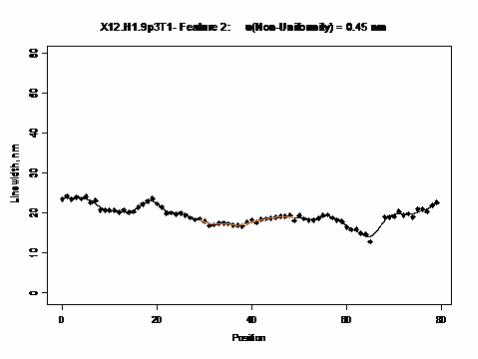
Plots taken from the CD-AFM measurements of the least and most uniform process
configurations are shown in figures 6 and 7. These figures illustrate the variation in measured
linewidth for each of the 80 scan lines that comprise each image – such as the example in figure 3.

14
The plots illustrate results of the best and worst process conditions observed in the experiment. As
can be seen in figure 7, we were able to achieve linewidths as low as 20 nm. The standard
uncertainty due to non-uniformity in the central 0.5 µm section of that feature, as defined by the
metric previously described, is 0.45 nm.
In figures 8 and 9 the normal probability plots are shown for both minimum linewidth and
non-uniformity. These plots were also based only the first five factors and the CD-AFM results on
the smallest width target prior to SEM inspection. The figures clearly demonstrate that statistically
significant conclusions can be drawn from the factor effects plots. Although the minimum CD has
some statistically significant dependence on two two-factor interactions, both of these involve pre-
thinning of the hard mask – which is the only factor that has a significant main effect – a
dependence we believe is well understood.
The non-uniformity exhibits a statistically significant dependence on two factors and one
two-factor interaction. As discussed above, the importance of the factor for etchant concentration
and etch time is not surprising, and the effect of ultra-sonic cleaning is also not unreasonable –
particularly considering that some of the apparent non-uniformity is probably due to residue on the
features. However, the significant dependence of the non-uniformity on the two-factor interaction
between ultra-sonic etch and cleaning duration is not fully understood. Further investigation of
significant effects identified in this experiment would be valuable, but we can conclude from these
results that this type of process is very well suited for applications such as CD-AFM tip calibration
standards.

15
3. SUMMARY AND PLANS
An important niche application of lattice-selective wet etching of silicon is the fabrication of
tip characterization standards for critical dimension atomic force microscopes (CD-AFMs). Since
accurate linewidth metrology using CD-AFM is critically dependent upon calibration of the tip
width, all applications of CD-AFM metrology are ultimately dependent upon tip calibration. At
least two NMIs have developed tip calibration standards for CD-AFM using lattice-selective
etching of silicon.
The NIST standard of this type is called the single crystal critical dimension reference
material (SCCDRM). These specimens, which are fabricated using a lattice-plane-selective etch on
(110) silicon, exhibit near vertical sidewalls and high uniformity and can be used to calibrate CD-
AFM tip width to a standard uncertainty of less than 1 nm.
In this paper we described an optimization experiment for the KOH etching of silicon
features such as those on the SCCDRMs. The results showed that it was possible to independently
tune the target linewidth and minimize the linewidth non-uniformity. We observed minimum
feature sizes of 20 nm and non-uniformity of less than 1 nm. Consequently, this process is
particularly well-suited for small-batch fabrication of CD-AFM tip calibration standards.
For potential refinement experiments in the future, we are considering other levels of the
etch factor and alternative cleaning processes which were considered too aggressive for the current
experiment. The so-called ‘piranha’ clean, which uses a mixture of sulphuric acid (H2SO4) and
hydrogen peroxide (H2O2), is one candidate. This cleaning process is commonly used in the micro-
electro-mechanical systems (MEMS) industry to remove resist and other organic residue.[21]

16
ACKNOWLEDGEMENTS
This work was supported by the Engineering Physics Division of the NIST Physical Measurement
Laboratory (PML).
*Address all correspondence to Ronald Dixson at [email protected]
†Certain commercial equipment is identified in this paper to adequately describe the experimental
procedure. Such identification does not imply recommendation or endorsement by the National
Institute of Standards and Technology nor does it imply that the equipment identified is necessarily
the best available for the purpose.

17
REFERENCES
1. D. B. Lee, “Anisotropic etching of silicon,” J. Appl. Phys. 40 (11), 4569-4574 (1969).
2. K. E Bean, “Anisotropic etching of silicon,” IEEE Trans. Electron Dev. 25 (10), 1185-1193
(1978).
3. D. L. Kendall, “Vertical etching of silicon at very high aspect ratios,” Ann. Rev. Mater. Sci. 9,
373-403 (1979).
4. H. Seidel et al., “Anisotropic etching of crystalline silicon in alkaline-solutions 1. Orientation
dependence and behavior of passivation layers,” J. Electrochem. Soc. 137 (11), 3612-3626
(1990).
5. E. S. Ammar and T. J. Rodgers, “UMOS transistors on (110) silicon,” IEEE Trans. Electron
Dev. 27 (5), 907-914 (1980).
6. E. Bassous and E. F. Baran, “Fabrication of high precision nozzles by anisotropic etching of
(100) silicon,” J. Electrochem. Soc. 125, 1321-1327 (1978).
7. S. K. Clark and K. D. Wise, “Pressure sensitivity in anisotropically etched thin-diaphragm
pressure sensors,” IEEE Trans. Electron Dev. 26, 1887-1896 (1979).

18
8. P. L. Chen, R. S. Muller, R. D. Jolly, G. L. Halac, R. M. White, A. P. Andrews, T. C. Lim, M.
E. Motamedi, “Integrated silicon microbeam PI-FET accelerometer,” IEEE Trans. Electron
Dev. 29, 27-33 (1982).
9. K. E. Peterson, A. Shartel, N. F. Raley, “Micromechanical Accelerometer Integrated with MOS
Detection Circuitry,” IEEE Trans. Electron Dev. 29, 23-27 (1982).
10. R. G. Dixson, R. A. Allen, W. F. Guthrie, and M. W. Cresswell, “Traceable Calibration of
Critical-Dimension Atomic Force Microscope Linewidth Measurements with Nanometer
Uncertainty,” J. Vac. Sci. Technol. B Vol. 23, 3028-3032 (2005).
11. M. Cresswell, W. Guthrie, R. Dixson, R. A. Allen, C. E. Murabito, J. V. Martinez de Pinillos,
“RM8111: Development of a Prototype Linewidth Standard,” J. Res. Natl. Inst. Stand. Technol.
111, 187 – 203 (2006).
12. G. Dai, M. Heidelmann, C. Kübel, R. Prang, J. Fuegge, and H. Bosse, “Reference nano-
dimensional metrology by scanning transmission electron microscopy,” Meas. Sci. Technol. 24,
085001 (2013).
13. G. Dai, F. Zhu, M. Heidelmann, G. Fritz, T. Bayer, S. Kalt, J. Fluegge, “Development and
characterisation of a new linewidth reference material,” Meas. Sci. Technol. 26, 115006 (2015).
14. Martin, H. K. Wickramasinghe, “Method for Imaging Sidewalls by Atomic Force Microscopy,”
Applied Physics Letters 64, 2498-2500 (1994).

19
15. I. Schmitz, M. Osborn, S. Hand, Q. Chen, “Improvement in metrology on new 3D-AFM
platform,” SPIE Proceedings Vol. 7122, 71222X (2008).
16. N. G. Orji, R. G. Dixson, A. Martinez, B. D. Bunday, J. A. Allgair, and T. V. Vorburger,
“Progress on implementation of a reference measurement system based on a critical-dimension
atomic force microscope,” J. Micro/Nanolith. MEMS MOEMS Vol. 6, 023002-1-10 (2007).
17. R. Dixson, N. G. Orji, C. D. McGray, J. Bonevich, J. Geist, “Traceable Calibration of a Critical
Dimension Atomic Force Microscope,” J. Micro/Nanolith. MEMS MOEMS Vol. 11, 011006
(2012).
18. M. Tortonese, G.F. Lorusso, R.M. Blanquies, J. Prochazka, L. Grella, “Sub-50-nm isolated line
and trench width artifacts for CD metrology,” SPIE Proceedings Vol. 5375, 647-656 (2004).
19. M. W. Cresswell, E. H. Bogardus, J. V. Martinez de Pinillos, M. H. Bennett, R. A. Allen, W. F.
Guthrie, C. E. Murabito, B. A. am Ende, L. W. Linholm, “CD Reference Materials for Sub-
Tenth Micrometer Applications,” SPIE Proceedings Vol. 4689, 116 - 127 (2002).
20. G. E. P. Box, W. G. Hunter, J. S. Hunter, “Statistics for Experimenters: An Introduction to
Design, Data Analysis, and Model Building,” Wiley-Interscience; 1st edition June 22 (1978).
21. C. A. Savran, A. W. Sparks, J. Sihler, J. Li, W. Wu, D. E. Berlin, T. P. Burg, "Fabrication and
characterization of a micromechanical sensor for differential detection of nanoscale motions,"
Journal of Microelectromechanical Systems, Vol. 11, 703 - 708, (2002).

20
Table I. Details of the SCCDRM process optimization experiment. For the 16 different
experimental treatments labeled as A through P, there were two chips processed at each
condition. The table shows the details of the treatments for the first five of the six two-level
factors used in the experiment. Factor 6 is the type of cleaning (acetone or ozone) used after an
SEM inspection, but it is not shown in the table because it is not central to etch optimization.
The overall experiment is a 26-2 fractional design with respect to all six factors. This method
allows estimation of all main effects and some two-factor interactions. (Note that the hard mask
removal step is not an independent factor but a complementary process step to factor 1 – since
total BOE time is fixed at 18 s.)
Process Step:
Pre-Thin Hard Mask (BOE)
Etchant Concentration and Etch Time
Ultrasonic Agitation During Etch
Hard Mask Removal(BOE)
Ultrasonic Agitation During IPA Cleaning
Duration of IPA Cleaning
Factor # 1 2 3 1* 4 5
Exp
erim
enta
l Tre
atm
ents
(A
th
ru P
)
A No 25 % KOH/25 s No 18 s No 30 s B 10 s 25 % KOH/25 s No 8 s No 100 s C No 25 % KOH/25 s No 18 s Yes 100 s D 10 s 25 % KOH/25 s No 8 s Yes 30 s E No 12.5 % KOH/35s No 18 s No 100 s F 10 s 12.5 % KOH/35s No 8 s No 30 s G No 12.5 % KOH/35s No 18 s Yes 30 s H 10 s 12.5 % KOH/35s No 8 s Yes 100 s I No 25 % KOH/25 s Yes 18 s No 30 s J 10 s 25 % KOH/25 s Yes 8 s No 100 s K No 25 % KOH/25 s Yes 18 s Yes 100 s L 10 s 25 % KOH/25 s Yes 8 s Yes 30 s M No 12.5 % KOH/35s Yes 18 s No 100 s N 10 s 12.5 % KOH/35s Yes 8 s No 30 s O No 12.5 % KOH/35s Yes 18 s Yes 30 s P 10 s 12.5 % KOH/35s Yes 8 s Yes 100 s
21
FIGURE CAPTIONS
Figure 1: Schematic of SOI starting material and SCCDRM process. For both prior generations
and current experiment, the device layer is approximately 160 nm thick and the buried oxide is
about 390 nm. The typical hard mask thickness is about 10 nm. Although earlier experiments used
a silicon nitride hard mask, oxide was used for both SCCDRM production and this optimization
experiment. The etchant used for this work was KOH.
Figure 2: Top down SEM image of an SCCDRM VLG target – as used for the HRTEM calibration
transfer to CD-AFM and also as the test target in the optimization experiment.
Figure 3: Wire-frame rendering of CD-AFM image of an SCCDRM VLG target similar to the one
in Figure 2. Note the apparent 90º rotation, because the fast scan axis is rendered horizontally, and
that a portion of the navigation marker is visible to the side of the image.
Figure 4: Factor effects plot for minimum linewidth. The most important single factor effect is pre-
thinning of the oxide hard mask prior to the silicon etch. (Notes: (1) Common background color
indicates confounded effects; (2) factor six is not included.)
Figure 5: Factor effects plot for linewidth non-uniformity. The most important single factor effect is
the etchant concentration and time. (Notes: (1) Common background color indicates confounded
effects; (2) factor six is not included.)
22
Figure 6: Example of CD-AFM data on feature from worst process condition. The plot shows the
linewidth calculated from individual linescans taken along a 2 µm length of the feature. The orange
curve indicates the portion of data used to calculate the non-uniformity metric.
Figure 7: Example of CD-AFM data on feature from best process condition. The plot shows the
linewidth calculated from individual linescans taken along a 2 µm length of the feature. The orange
curve indicates the portion of data used to calculate the non-uniformity metric.
Figure 8: Normal probability plot for factor effects on minimum linewidth showing the dramatic
dependence on pre-thinning of the hard mask (factor 1) and statistical significance of the
observation. (The numbers next to the data points indicate the associated factor or factors for two-
factor interactions.)
Figure 9: Normal probability plot for factor effects on linewidth non-uniformity showing the
statistical significance of three effects with the largest being the factor for etch time and etchant
concentration (factor 2). (The numbers next to the data points indicate the associated factor or
factors for two-factor interactions.)

23
Ronald Dixson is a physicist in the Physical Measurement Laboratory (PML) of the National
Institute of Standards and Technology (NIST). His current research interests are calibration
methods, traceability, and uncertainty analysis in atomic force microscope (AFM) dimensional
metrology – including the NIST traceable AFM (T‐AFM) project and metrology applications of
critical dimension AFM (CD‐AFM). He holds a Ph.D. in Physics and is a member of SPIE, AVS, and
the American Physical Society.
William F. Guthrie has been a statistician in the Statistical Engineering Division at NIST for the last
26 years, and he is currently serving as the Chief of that division. He collaborates with NIST
researchers in a wide range of areas including semiconductor and microelectronics applications,
building materials applications and chemical science applications. His statistical interests include
design of experiments, uncertainty assessment, calibration, modem regression methods, Bayesian
statistics, and statistical computation. He holds a B.A. in Mathematics from Case Western Reserve
University and an M.S. in Statistics from the Ohio State University at Columbus.
Richard A. Allen is a Physicist in the Engineering Physics Division at NIST, where his research areas
are microdevices, motion metrology, and methods for calibration of accelerometers. He is a Co‐
Chair of the SEMI 3DS‐IC Standards Committee and was NIST assignee to SEMATECH’s 3D
Enablement Center from 2011‐2013. Mr. Allen received the B.S. and M.S., both in Physics, from
Rensselaer Polytechnic Institute and his M.B.A. from Columbia Union College.

24
Ndubuisi G. Orji is a mechanical engineer in the Physical Measurement Laboratory of the National
Institute of Standards and Technology (NIST). His research interests are in atomic force
microscopy, surface metrology, nano‐scale dimensional metrology, and optical metrology. He
holds a PhD in mechanical engineering from the University of North Carolina at Charlotte. He is a
Michael W. Cresswell served for 19 years as a Senior Engineer at NIST in the former Electronics and
Electrical Engineering Laboratory (EEEL) – now part of the Physical Measurement Laboratory of the National
Institute of Standards and Technology (NIST) and continued to serve as a contractor for five subsequent
years. His research interest was developing methods for micro‐machining crystalline structures to serve as
reference materials for nanometer‐scale critical‐dimension metrology. He holds a PhD in physics from the
Pennsylvania State and served a member of the American Physical Society. He is also a life‐member of the
Institute of Electrical and Electronic Engineers.
Christine E. Murabito– bio unavailable


Related Documents


