Preparation and characterization of CdS nanoparticles Dissertation zur Erlangung des Naturwissenschaftlichen Doktorgrades der Bayerischen Julius-Maximiliams-Universität Würzburg Vorgelegt von Sanjeev Joshi aus Pune, Indien Würzburg, 2004

Welcome message from author
This document is posted to help you gain knowledge. Please leave a comment to let me know what you think about it! Share it to your friends and learn new things together.
Transcript

Preparation and characterization of CdS nanoparticles
Dissertation zur Erlangung des Naturwissenschaftlichen Doktorgrades
der Bayerischen Julius-Maximiliams-Universität Würzburg
Vorgelegt von
Sanjeev Joshi
aus Pune, Indien
Würzburg, 2004

Eingereicht am 5. Juli 2004 bei der Fakultät für Physik und Astronomie
1. Gutachter: Prof. Dr. E. Umbach 2. Gutachter: Prof. Dr. Ossau
der Dissertation
1. Prüfer: Prof. Dr. E. Umbach 2. Prüfer: Prof. Dr. W. Kinzel
der mündlichen Prüfung Tag der mündlichen Prüfung: 19/07/2004 Doktorurkunde ausgehändigt am: ..............

To my beloved wife and son,
Truth, Purity and unselfishness
Whenever these are there,
There is no power below or
Above the Sun
To crush the possession there off
Equipped with these
One individual can face the whole
Universe in opposition
--Vivekananda
(The great Indian Philosopher)


Zusammenfassung CdS-Nanoteilchen mit Größen zwischen 1.1 und 4.2 nm wurden in Äthanol und mit Thioglycerol (TG)-Hülle synthetisiert. Es wurde gezeigt, dass die nass-chemische Synthese ohne Wasser und die Verwendung von TG als Hülle folgende Vorteile bieten: Es konnten kleinere Teilchen hergestellt und eine schmalere Größenverteilung erzielt werden. Zusätzlich wird dem Altern der Teilchen vorgebeugt, und die Ergebnisse sind besser reproduzierbar. Hochaufgelöste Photoemissions-Messungen an kleinen CdS-Teilchen (1.1, 1.4, 1.7, 1.8; 1.8 nm mit Glutathion-Hülle) ergaben Beiträge von fünf verschiedenen Schwefelatom-Typen zum S 2p-Gesamt Signal. Außerdem wurde beobachtet, dass Nanoteilchen unterschiedlicher Größe und/oder mit unterschiedlichen Hüllen-Substanzen verschiedene Photoemissionsspektren zeigen und verschieden starke Strahlenschäden aufweisen. Bei den 1.4 nm großen CdS-Teilchen entsprechen die Komponenten des S 2p-Signals entweder Schwefelatomen mit unterschiedlichen Cd-Nachbarn, Thiol-Schwefelatomen oder teilweise oxidiertem Schwefel. Die jeweilige Zuweisung der Schwefeltypen erfolgte über Intensitäts-Änderungen der einzelnen S 2p-Komponenten als Funktion der Photonenenergie und des Strahlenschadens. Die Daten der 1.4 nm großen CdS-Teilchen wurden mit PES-Intensitäts-Rechnungen verglichen, die auf einem neuen Strukturmodell-Ansatz basieren. Von den drei verwendeten CdS-Strukturmodellen konnte nur ein Modell mit 33 S-Atomen die Variation der experimentellen Intensitäten richtig wieder geben. Modelle von größeren Nanoteilchen mit beispielsweise 53 S-Atomen zeigen Abweichungen von den experimentellen Daten der 1.4 nm-Teilchen. Auf diese Weise kann indirekt auf die Größe der gemessenen Teilchen geschlossen werden. Die Intensitätsrechnungen wurden zum einen „per Hand“ zur groben Abschätzung durchgeführt, zum anderen wurden exaktere Berechnungen mit einem von L. Weinhardt und O. Fuchs entwickelten Programm angestellt. Diese bestätigen die Ergebnisse der Abschätzung. Zudem wurde festgestellt, dass die inelastische freie Weglänge λ keinen signifikanten Einfluss auf die Modellrechnungen hat. Die gemessenen Intensitäts-Änderungen konnten zwar mit mehreren leicht verchiedenen Modellen erklärt werden, allerdings führte nur ein kugelförmiges Teilchen-Modell auch zu den richtigen Intensitätsverhältnissen der einzelnen S 2p-Komponenten. Weiterhin konnte beobachtet werden, dass die elektronische Bandlücke größer ist als die optische Bandlücke. Bei den PES-Messungen wurden einige wichtige Einflüsse sichtbar. So spielen strahlenbedingte Effekte eine große Rolle. Kenntnisse über die Zeitskala solcher Effekte ermöglichen PES-Aufnahmen mit guter Signal-Qualität und erlauben eine Extraploation zur Situation ohne Strahlenschaden. Auch die Dünnschicht-Präparation beeinflusst die Spektren. Beispielsweise zeigten mit Elektrophorese hergestellte Filme Hinweise auf Agglomeration. Schichten, die per Tropfen-Deposition erzeugt wurden, weisen spektrale Änderungen am Rand der Probe auf, und Filme aus Nanoteilchen-Pulver waren nicht homogen. Mikro-Raman Experimente, die in Kollaboration mit Dr. M. Schmitt und Prof. W. Kiefer durchgeführt wurden, ließen große Unterschiede in den Spektren von Nanoteilchen und TG in Lösung erkennen. Dies wurde vor allem auf das Fehlen von S – H –Bindungen zurückgeführt und zeigt damit, dass alle TG-Moleküle verwertet oder ausgewaschen wurden.


Contents
1. Introduction 9
2. Literature survey of quantization effects and size determination in 13
semiconductor nanoparticles
2.1 Size confinement effect (SCE) 13
2.2 Determination of particle size 18
3. Experimental 21
3.1 Methods 21
3.2 Experimental work of this thesis 24
4. Preparation of CdS nanoparticles 27
4.1 Overview of various synthesis techniques for CdS nanoparticles 27
4.2 Wet chemical synthesis of thioglycerol (TG) capped CdS nanoparticles 28
4.2.1 Aqueous and non-aqueous methods 31
4.2.2 Monodispersity: a comparison of TG and MPA capping 31
4.2.3 Size-selective precipitation 34
4.3 Thin film preparation 37
5. High-resolution photoemission study of CdS nanoparticles 39
5.1 Results: differently sized particles look very different 39
5.2 Assignment of spectral sulfur components 43
5.3 Model based intensity calculations for CdS-B 46
5.4 Inelastic mean free path of electrons 50
5.5 Development of a suitable program for the model-based intensity 53
calculation (with L. Weinhardt and O. Fuchs)
5.5.1 Plausibility checks for the program 54
5.5.2 Application of the program to the structural models 58
5.6 Summary 62
6. Band gap opening in CdS nanoparticles (NEXAFS+VBPES) 65
7. Additional investigations of CdS nanoparticles 69
7.1 Laboratory XPS investigations of nanoparticle films 69
7.2 Thermal stability of CdS nanoparticles 72
7.3 Effects of beam damage 73
7.4 Influences of the thin film preparation methods 76
7.5 Raman: Comparison of TG and CdS nanoparticles (with C. Dem and 78
M. Schmitt)
7.6 Summary 81
8. Summary and outlook 83
9.Bibliography 85
9
Chapter 1 Introduction
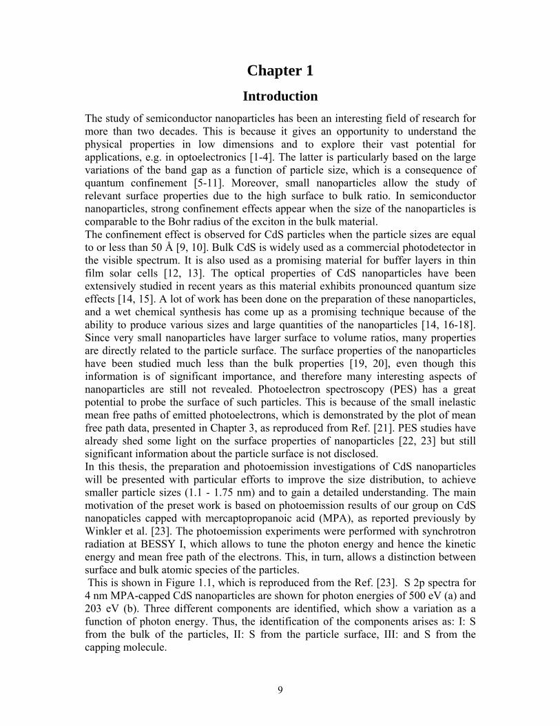
The study of semiconductor nanoparticles has been an interesting field of research for more than two decades. This is because it gives an opportunity to understand the physical properties in low dimensions and to explore their vast potential for applications, e.g. in optoelectronics [1-4]. The latter is particularly based on the large variations of the band gap as a function of particle size, which is a consequence of quantum confinement [5-11]. Moreover, small nanoparticles allow the study of relevant surface properties due to the high surface to bulk ratio. In semiconductor nanoparticles, strong confinement effects appear when the size of the nanoparticles is comparable to the Bohr radius of the exciton in the bulk material. The confinement effect is observed for CdS particles when the particle sizes are equal to or less than 50 Å [9, 10]. Bulk CdS is widely used as a commercial photodetector in the visible spectrum. It is also used as a promising material for buffer layers in thin film solar cells [12, 13]. The optical properties of CdS nanoparticles have been extensively studied in recent years as this material exhibits pronounced quantum size effects [14, 15]. A lot of work has been done on the preparation of these nanoparticles, and a wet chemical synthesis has come up as a promising technique because of the ability to produce various sizes and large quantities of the nanoparticles [14, 16-18]. Since very small nanoparticles have larger surface to volume ratios, many properties are directly related to the particle surface. The surface properties of the nanoparticles have been studied much less than the bulk properties [19, 20], even though this information is of significant importance, and therefore many interesting aspects of nanoparticles are still not revealed. Photoelectron spectroscopy (PES) has a great potential to probe the surface of such particles. This is because of the small inelastic mean free paths of emitted photoelectrons, which is demonstrated by the plot of mean free path data, presented in Chapter 3, as reproduced from Ref. [21]. PES studies have already shed some light on the surface properties of nanoparticles [22, 23] but still significant information about the particle surface is not disclosed. In this thesis, the preparation and photoemission investigations of CdS nanoparticles will be presented with particular efforts to improve the size distribution, to achieve smaller particle sizes (1.1 - 1.75 nm) and to gain a detailed understanding. The main motivation of the preset work is based on photoemission results of our group on CdS nanopaticles capped with mercaptopropanoic acid (MPA), as reported previously by Winkler et al. [23]. The photoemission experiments were performed with synchrotron radiation at BESSY I, which allows to tune the photon energy and hence the kinetic energy and mean free path of the electrons. This, in turn, allows a distinction between surface and bulk atomic species of the particles. This is shown in Figure 1.1, which is reproduced from the Ref. [23]. S 2p spectra for 4 nm MPA-capped CdS nanoparticles are shown for photon energies of 500 eV (a) and 203 eV (b). Three different components are identified, which show a variation as a function of photon energy. Thus, the identification of the components arises as: I: S from the bulk of the particles, II: S from the particle surface, III: and S from the capping molecule.

10
In the present case we have very small particles capped with thioglycerol (TG) instead of MPA and expect a larger surface to bulk ratio. Furthermore, we perform photoemission measurements using the undulator beam line at BESSY II (a third generation synchrotron radiation source), which produces very high flux, and a SCIENTA electron analyser for higher resolution. This facilitates the spectral separation of the different components of the photoemission data, and we can expect to reveal more than three S species in these particles, if present. We have put much effort in the wet chemical preparation of the CdS nanoparticles (which was introduced to our group by S. K. Kulkarni, our collaborator from Pune, India) to achieve small sizes and to narrow the size distribution using TG as a capping agent (TG was used for ZnS nanoparticles in the Pune laboratory for the last few years, showing very promising results [24-27]). Chapter 2 gives a short overview of the theoretical basis behind the work presented in this thesis. Conventional methods for the size
determination of the nanoparticles and the limitations of these techniques are discussed in brief at the end of Chapter 2. A short description of the used experimental methods and details of the experimental work are presented in Chapter 3. Chapter 4 deals with the details of the preparation of CdS nanoparticles, concentrating on the production of smaller sizes and monodispersed particles. We will see that in wet chemical preparation, non-aqueous synthesis is better as it gives access to smaller sizes, prohibits aging of the particles, and shows reproducibility compared to aqueous synthesis. We will demonstrate that the size distribution is narrowed with TG compared to MPA capping. Furthermore, we will present results of size selective precipitation used to produce mondispersed CdS nanoparticles. The details of the analysis of high-resolution photoemission data are presented in Chapter 5. We will see that there are five different S components representing the data. A new approach of data evaluation with the help of a structural model is introduced (built from an XRD analysis done by C. Kumpf). Photoemission intensity calculations
Figure 1.1: S 2p photoemission spectra for wet
chemically prepared CdS nanoparticles using
mercaptopropanoic acid (MPA) capping as
reproduced from reference [23]. The spectra are
recorded for photon energies of 500 eV (a), i.e.,
bulk sensitive and 203 eV (b), i.e., surface
sensitive.

11
are necessary in order to understand the intensity contributions and variations. It will be demonstrated that with this approach the different S components can be assigned as S species with different Cd neighbours. The results of this approach are confirmed using a suitable program for the intensity calculations developed with L. Weinhardt and O. Fuchs. Furthermore, the effects of inelastic mean free paths and the particle shapes are also checked. Finally, a short overview of the determination of inelastic mean free paths is included in this chapter. We shall estimate the mean free path for the photon energies we are using by two different formulas, and use the average value for the intensity calculation in the program. It can be seen that this approach offers an indirect way of size and shape determination of nanoparticles applied to CdS in the present case. Chapter 6 deals with a band gap opening study of CdS nanoparticles, using a combination of valence band photoemission spectroscopy (VBPES) and near-edge x-ray absorption spectroscopy (NEXAFS). Additional investigations of the nanoparticles are presented in Chapter 7. We will focus on the following aspects in this chapter: influence of the thin film preparation method, particle termination, oxidation, thermal stability, and photoemission spectral variations as a function of spot and beam exposure time. A comparison of TG molecules in solution and TG-capped CdS nanoparticles with micro-Raman measurements (in collaboration with the group of Dr. M. Schmidt and Prof. W. Kiefer) will be presented at the end of this chapter.

12

13
Chapter 2
Literature survey of quantization effects and size determination of
semiconductor nanoparticles A theory of size confinement in semiconductor nanoparticles is well described in text books [1, 2] and reported partly in some previous doctoral theses [27, 28]. Also an article by H. Weller gives a very nice introduction and overview of theoretical progress focusing on size quantization effects [29]. This chapter also gives an overview of size confinement effect in order to create a background behind the work presented in this thesis. At the end of this chapter various conventional methods for the size determination of nanoparticles are listed with a short description of previous work using these techniques. It is emphasized that conventional methods do not give an exact information abut the particle size. Thus, we like to add new aspects of size determination with the help of photoemission results as a part of the work presented in this thesis.
2.1 Size confinement effect (SCE) In semiconductors a fundamental optical absorption process may occur if the photon energy is larger than the band gap thus creating an electron and a hole. This electron-hole (e-h) pair can move independently of one another resulting in electrical conductivity. The separation of the electron and the hole usually is large enough so that there is no Coulombic attraction between them. Such description of non-interacting electrons and holes corresponds to the so called single particle presentation. If the absorption occurs at Γ point ( k = 0) and with a photon energy slightly below the band gap, electrons and holes do interact via Coulomb potential and form quasiparticle that corresponds to a hydrogen-like bound state of an e-h pair which is referred to as an exciton. In conventional semiconductors the excitons are classified as weakly bound Mott - Wannier excitons, for which the e-h distance is large in comparison with the lattice constant, while a strongly bound Frenkel exciton with an e-h distance comparable to the lattice constant occurs in ionic or rare gas crystals and in organic materials. The Wannier exciton resembles a hydrogen atom. Therefore, similarly to the hydrogen atom, this exciton is characterized by the exciton Bohr radius (aB)
where ε is the dielectric constant, and me and mh is the electron and hole eeddwdemass, respectively. The effective e-h mass is smaller than the electron mass me, and the dielectric constant is several times larger than 1. This is why the exciton Bohr radius is significantly larger and the exciton Rydberg energy, Ry∗( Ry∗ = e2/2εaB) is significantly smaller than the relevant values of the hydrogen atom. Absolute values of aB for the common
14
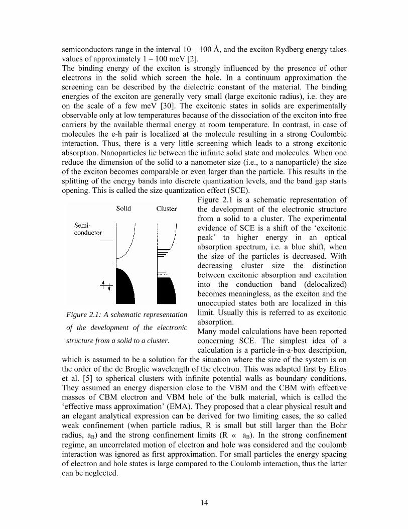
semiconductors range in the interval 10 – 100 Å, and the exciton Rydberg energy takes values of approximately 1 – 100 meV [2]. The binding energy of the exciton is strongly influenced by the presence of other electrons in the solid which screen the hole. In a continuum approximation the screening can be described by the dielectric constant of the material. The binding energies of the exciton are generally very small (large excitonic radius), i.e. they are on the scale of a few meV [30]. The excitonic states in solids are experimentally observable only at low temperatures because of the dissociation of the exciton into free carriers by the available thermal energy at room temperature. In contrast, in case of molecules the e-h pair is localized at the molecule resulting in a strong Coulombic interaction. Thus, there is a very little screening which leads to a strong excitonic absorption. Nanoparticles lie between the infinite solid state and molecules. When one reduce the dimension of the solid to a nanometer size (i.e., to a nanoparticle) the size of the exciton becomes comparable or even larger than the particle. This results in the splitting of the energy bands into discrete quantization levels, and the band gap starts opening. This is called the size quantization effect (SCE).
Figure 2.1 is a schematic representation of the development of the electronic structure from a solid to a cluster. The experimental evidence of SCE is a shift of the ‘excitonic peak’ to higher energy in an optical absorption spectrum, i.e. a blue shift, when the size of the particles is decreased. With decreasing cluster size the distinction between excitonic absorption and excitation into the conduction band (delocalized) becomes meaningless, as the exciton and the unoccupied states both are localized in this limit. Usually this is referred to as excitonic absorption. Many model calculations have been reported concerning SCE. The simplest idea of a calculation is a particle-in-a-box description,
which is assumed to be a solution for the situation where the size of the system is on the order of the de Broglie wavelength of the electron. This was adapted first by Efros et al. [5] to spherical clusters with infinite potential walls as boundary conditions. They assumed an energy dispersion close to the VBM and the CBM with effective masses of CBM electron and VBM hole of the bulk material, which is called the ‘effective mass approximation’ (EMA). They proposed that a clear physical result and an elegant analytical expression can be derived for two limiting cases, the so called weak confinement (when particle radius, R is small but still larger than the Bohr radius, aB) and the strong confinement limits (R « aB). In the strong confinement regime, an uncorrelated motion of electron and hole was considered and the coulomb interaction was ignored as first approximation. For small particles the energy spacing of electron and hole states is large compared to the Coulomb interaction, thus the latter can be neglected.
Figure 2.1: A schematic representation
of the development of the electronic
structure from a solid to a cluster.

15
A further development of the theory introduced modifications of the EMA by adding the Coulomb interaction. Brus et al. [6] reported that an independent treatment of the electron and hole is not justified and the problem of two particles Hamiltonian with kinetic energy terms, Coulomb interaction, and confinement potential should be examined. Contrary to a hydrogen like Hamiltonian, the appearance of a confinement potential does not allow a center of mass motion. The motion of the particle has to be considered independently. They calculated the energy of ground state of the electron hole pair in which the term proportional to e2/εR describes the effective e-h interaction (see Eq. 1). Kayanuma et al. [8] considered a correlation energy due to the polarization of the crystal and derived an equation for all size regimes:
(Eq. 1)
where R is the cluster radius and E*Ry is the effective Rydberg energy e4/2ε2h2(me-1 + mh-1). The first term in the equation represents the particle-in-a-box quantum localization energy and has a simple 1/R2 dependence [5]. The second term represents the Coulomb energy with a 1/R dependence [6]. And the third term is a result of the spatial correlation effect [8]. One can see that the effective Coulomb e-h interaction by no means vanishes in small particles. The correlation energy is generally small compared to the kinetic energy and the e-h Coulomb energy (e.g. for CdS, about 7 % of the total energy). However it could be significant if the semiconductor has a small dielectric constant. Another modification to the EMA concerns the infinite potential walls. For clusters in the strong confinement regime the assumption of infinite height is poor. Several authors reported [7, 8, 31-33] calculations considering finite potential walls and showed that this correction becomes significant for small clusters. The influence of the finite potential walls on the energy states increases with decreasing cluster size and with increasing quantum number for a given cluster. Thoai et al. [34] provided absolute values for this effect. For CdS clusters, a comparison of infinite potential walls with the values of finite potential walls as provided by Schooss et al. [35] confirms that smaller clusters are significantly influenced by this. Furthermore, the CB electron is much more affected than the VB hole, which is reasonable as the CB electron has a four times smaller effective mass than the VB hole. Equation 1, although containing the basic physics of the quantum size effect, cannot be expected to be quantitatively correct, especially for very small clusters. This is because for small clusters the eigenvalues of the lowest excited states are located in a region of the energy band that is no longer parabolic (breakdown of the effective mass approximation). The effective masses should increase with decreasing cluster size as one would expect that the curvatures of the lowest CB and highest VB decrease with decreasing cluster size. The effective masses are determined by the periodic potential of the crystal and hence can differ for small particles (as their lattice structure may be very different from that of bulk). A possible correction in this direction was adopted by Nomura et
16
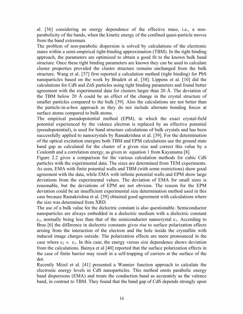
al. [36] considering an energy dependence of the effective mass, i.e., a non-parabolicity of the bands, when the kinetic energy of the confined quasi-particle moves from the band extremum. The problem of non-parabolic dispersion is solved by calculations of the electronic states within a semi-empirical tight-binding approximation (TBM). In the tight binding approach, the parameters are optimized to obtain a good fit to the known bulk band structure. Once these tight binding parameters are known they can be used to calculate cluster properties provided the cluster structure remains unchanged from the bulk structure. Wang et al. [37] first reported a calculation method (tight binding) for PbS nanoparticles based on the work by Brudett et al. [38]. Lippens et al. [10] did the calculations for CdS and ZnS particles using tight binding parameters and found better agreement with the experimental data for clusters larger than 20 Å. The deviation of the TBM below 20 Å could be an effect of the change in the crystal structure of smaller particles compared to the bulk [39]. Also the calculations are not better than the particle-in-a-box approach as they do not include alternate bonding forces at surface atoms compared to bulk atoms. The empirical pseudopotential method (EPM), in which the exact crystal-field potential experienced by the valence electron is replaced by an effective potential (pseudopotential), is used for band structure calculations of bulk crystals and has been successfully applied to nanocrystals by Ramakrishna et al. [39]. For the determination of the optical excitation energies both TBM and EPM calculations use the ground state band gap as calculated for the cluster of a given size and correct this value by a Coulomb and a correlation energy, as given in equation 1 from Kayanuma [8]. Figure 2.2 gives a comparison for the various calculation methods for cubic CdS particles with the experimental data. The sizes are determined from TEM experiments. As seen, EMA with finite potential walls and TBM (with some restrictions) show good agreement with the data, while EMA with infinite potential walls and EPM show large deviations from the experimental values. The deviation of EMA for small sizes is reasonable, but the deviations of EPM are not obvious. The reason for the EPM deviation could be an insufficient experimental size determination method used in this case because Ramakrishna et al. [39] obtained good agreement with calculations where the size was determined from XRD. The use of a bulk value for the dielectric constant is also questionable. Semiconductor nanoparticles are always embedded in a dielectric medium with a dielectric constant ε2, normally being less than that of the semiconductor nanocrystal ε1. According to Brus [6] the difference in dielectric constants gives rise to surface polarization effects arising from the interaction of the electron and the hole inside the crystallite with induced image charges outside. The polarization effects are more pronounced in the case where ε2 « ε1. In this case, the energy versus size dependence shows deviation from the calculations. Bainya et al [40] reported that the surface polarization effects in the case of finite barrier may result in a self-trapping of carriers at the surface of the dot. Recently Mizel et al. [41] presented a Wannier function approach to calculate the electronic energy levels in CdS nanoparticles. This method omits parabolic energy band dispersions (EMA) and treats the conduction band as accurately as the valence band, in contrast to TBM. They found that the band gap of CdS depends strongly upon

17
number of unit cells in the nonocrystal but only weakly on their arrangement, i.e. on the shape of the particle. We are dealing with the very small size regime of nanoparticles in this thesis, i.e., nanoparticles from 1 nm to 4 nm in diameter. It is important to note that all theoretical models are hardly suitable for the nanoparticles in this size regime. This is because of only few tens of atoms in the particle which can be better represented by a molecular approach than by a solid state approach as in the above models. Also, the very high surface to bulk ratio of these nanoparticles create the necessity for consideration of larger surface effects within the theoretical approach. We end the overview of size quantization effects by writing a small paragraph on size dependent oscillator strengths, which are important concerning the UV absorption spectra of nanoparticles. As mentioned before it is experimentally observed in many investigations that with decreasing cluster size the energy gap increases. These investigations also indicated that as the particle size is reduced the excitonic peak becomes sharper. This is because of a rise of the oscillator strength of the exciton for small particles. In small clusters the e-h pair is spatially confined. The effect of such confinement on the exciton spectrum has been discussed in detail by Kayanuma [32]. It is known that the exciton oscillator strength is given by [42]
Figure 2.2: A comparison of theoretical methods for the size confinement effect in cubic
CdS nanoparticles with experimental data (shown by filled black circles).

18
where m is the electron mass, ∆E is the transition energy, µ is the transition dipole moment, and ⏐U(0)⏐2 represents the probability of finding the electron and the hole on the same site (the overlap factor). The total oscillator strength per cluster, fcluster, determines the radiative lifetime in the 0 K limit, and the oscillator strength per unit volume, fcluster / V ( V is the volume of the cluster), determines the absorption coefficient. The absorption coefficient here refers to that of clusters, which can be obtained by dividing the absorption coefficient of the sample (consisting of clusters diluted in a certain medium) by the volume fraction of the clusters. For clusters with R « aB, the overlap between the electron and hole wave function, ⏐U(0)⏐2, increases with decreasing cluster volume. As a result, fcluster is only weakly dependent on the cluster size in this size regime. However, the oscillator strength per unit volume, fcluster / V, now increases with decreasing cluster size and scales approximately with (aB / R )3 (ignoring the ∆E factor). Since fcluster / V determines the absorption coefficient, the exciton absorption band should get stronger with decreasing cluster size in the R « aB regime and become visible even at room temperature. Furthermore, it is illustrated how the exciton strength varies with partical size. For R = 10 aB, i.e. for larger clusters the exciton states below zero (i.e the conduction band edge of the semiconductor) are occupied and very closely spaced. The spacing increases for R = 5 aB, and for a particle with a size equal to the Bohr radius, i. e. R = 1 aB, the exciton state is above the conduction band edge of the material. Also there is an increase of fcluster / f (ratio of the oscillator strength in the nanoparticle over the oscillator strength in bulk) by an order of magnitude [32].
2.2 Determination of the nanoparticle size What is the real size of the nanoparticle ? This is a fundamental question specially for the nanoparticles synthesized with organic capping molecules. Importantly no size determination technique allows an exact size determination. The difficulty arises mainly because of the limitations of the available methods and also because of the influence of the capping molecules attached to the particle surface. The methods used conventionally to determine particle sizes are listed below.
1) UV-VIS absorption 2) X Ray Diffraction (XRD) 3) Transmission Electron Microscopy (TEM) 4) Scanning tunnelling Microscopy (STM) 5) Atomic Force Microscopy (AFM) 6) Small angle X-ray Scattering (SAXS)
UV-VIS absorption is a very first characterization method for the nanoparticles because the absorption features give information about the nanoparticle formation, the band gap and the size distribution of the nanoparticles. However, it is an indirect method for determining the particle size. The band gap of the particles can be calculated from the excitonic peak position, which is used to determine the particle size with the help of curves of energy gap versus size obtained from theoretical models such as EMA or TBM (see section 2.1). As discussed in section 2.1, TBM gives a

19
better description for the smaller sizes [10], and therefore a TBM curve is referred in this thesis for the estimation of sizes of our nanoparticles. X-ray powder diffraction was used for structure and size determination by many groups [37, 43 - 47]. There are some reports which exclusively focus on the crystal structure determination of Zn or Cd (S, Se) cluster complexes and [46] and CdS clusters [47]. The particle size can be obtained either by direct computer simulation of the X-ray diffraction pattern or from the full width at half maximum (FWHM) of the diffraction peaks using the Debye-Scherrer formula [48]. The line width depends on the crystalline regions within the particle. When the particles are not perfectly crystalline a problem arises in the size estimation. Particles smaller than 25 Å lead to significant broadening of the line width [49]. Furthermore, the validity of Scherrer’s equation, the effect of defects, shapes and size distributions on the X-ray diffraction patterns has to be examined. This is possible with a direct computer simulation approach. Bawendi et al. [43] have reported a comparison of experimental and simulated X-ray powder diffraction spectra in combination with TEM imaging mainly to describe the average nanoparticle structure. The comparison of experimental XRD data with simulated XRD pattern for a 35 Å diameter spherical particle was done for different shapes and lattice disorders. A new approach similar to this is followed in our group in order to estimate the size of the nanoparticles prepared by wet chemical synthesis which is discussed later in the text [50]. Electron microscopy is widely used to determine the size of particles [14, 51 - 56]. TEM allows the imaging of individual particles and to some extent to evaluate the statistical distribution of sizes and shapes of the particles in sample. High magnification imaging with lattice contrast allows imaging of individual crystallite morphologies [44]. It is possible to detect smaller particles such as 50 Å in diameter as reported by Weller et al [51]. However, TEM is a local probe because only particles in a very small area can be probed, and it is not possible to get an impression of a large number of particles that are statistically oriented. Furthermore, it is tricky to find individual particles, and only a part of such particles can be seen under the microscope from which an information on the shape and size is not completely disclosed. The use of STM in size determination was adopted by a few groups [57 - 59] for a range of ZnS particles. Wang et al. [57] and Coury et al. [58] thus confirmed the results of size determination obtained by XRD with STM. They also employed AFM in this direction. AFM measurements give good information about the overall morphology of the nanoparticle films. Previously in our group, nanoparticles were characterized by AFM for different synthesis methods, film preparation, and instrumental parameters [60]. It is possible to extract some information about the particle shape and size from the AFM image but difficulties arise especially for very small nanoparticles (~ 1 nm) because of the greater influence of the substrate. Moreover, the particles should be large enough and should not coalesce on the substrate. Furthermore, AFM is also a local probe and, similar to TEM, it does not give the statistical information about the particles. Small angle X-ray scattering (SAXS) definitely adds to the knowledge of size and shape of nanoparticles. A better description of the data of ZnS particles was found with rod-like particle shapes in a previous work by Dhyagude et al. [61]. However, a reliable analysis was not possible because a suitable program to fit the SAXS data was under debate, and the model assumptions could have a significant influence on the

20
results. Recently, this problem was solved and further investigation of SAXS data was carried out by Vogel et al. [61], which revealed that the particles are mass fractals that aggregate via a reaction limited process to form irregular but rather dense network. In summary, an exact information about size, shape and size distribution of nanoparticles is not yet completely disclosed because of technical limitations of the various size determination methods. The size confinement effect is reflected in every experiment done to characterize the nanoparticles. The size sensitivity of other non-conventional techniques (for size determination) can be used indirectly to get information about the size. It will be shown in this thesis that high-resolution photoemission data not only give valuable information on the nanoparticle surface but also indicate the size dependency. A new approach in the analysis of photoemission spectra is taken in order to extract useful information in this direction as will be seen in chapter 5. It is hoped that this approach will add to the information on the size aspect of the particles and open a new way of size determination of very small particles by a non-conventional technique.
21
Chapter 3
Experimental The main experimental method used in the framework of this thesis is photoelectron spectroscopy (PES) coupled with synchrotron radiation for surface characterization. The other methods also applied were UV-VIS spectroscopy, X-ray diffraction (XRD), Raman spectroscopy, and near edge x-ray absorption spectroscopy (NEXAFS) in order to gain additional information on nanoparticles. The first section of this chapter gives a brief introduction of the photoemission and x-ray absorption techniques. Further information about these techniques can be found in the books of Briggs and Seah [21], Hüfner [62], Fadley [63], and Stöhr [64]. The second section contains a description of the experimental aspects of the work presented in this thesis. 3.1 Methods 1) Photoelectron Spectroscopy (PES) In photoelectron spectroscopy the sample under investigation is irradiated by photons (X-rays, UV radiation), which causes the excitation of electrons. These photon-excited electrons or photoelectrons, if emitted from the surface, are analyzed with respect to their kinetic energy. Figure 3.1 shows a schematic of the photoemission process. The technique is classified based on the excitation energy as X-ray photoelectron spectroscopy (XPS) or ultraviolet photoelectron spectroscopy (UPS). The energy of the detected photoelectrons contains information about the binding energy of the initial state. The binding energy Eb (referred to the Fermi level) is defined as the difference in total energy between the final and the initial state and can be written in a simple expression as follows:
Eb = Einitial – Efinal = hν – Ek – Φ, where hν is the energy of the exciting photon, Ek is the kinetic energy of the photoelectron with respect to the vacuum level, and Φ is the work function. The work function is defined as the difference between the potential far outside the solid surface (i.e., the vacuum level) and the Fermi energy inside the solid which is equal to the chemical potential of a solid at 0 K. The final state of the photoemission process is associated with the presence of a core hole. The whole electronic system responds to this core hole by screening on a time scale of 10-15 to 10-17 seconds [21]. After roughly 10-15 s, the core hole is filled by an electron from an energetically higher state and the energy difference is emitted as photon (X-ray emission) or Auger electron. The majority of the (shallow) core hole decay processes occurs via Auger electron emission.

22
Figure 3.1: Schematic of the photoemission process. An electron from a core or valence level is ejected. This is referred to as XPS (x-ray photoelectron spectroscopy) and UPS (UV photoelectron spectroscopy), respectively. The photoemission gives not only qualitative and quantitative information of the various species in the sample under investigation but also probes the different chemical environment surrounding the species. Furthermore, it is a surface sensitive technique because even though the ionization occurs to a depth of 10 – 1000 nm by photons depending on energy and material, only those electrons that originate within few tens of Angstroms below the solid surface can leave the surface without energy loss. The distance travelled by an electron in the sample before being inelastically scattered is characterized by the inelastic mean free path (λ). PES is limited to study surface regions of solids as demonstrated by the plot of mean free path values of electrons for an energy range of 0.3 eV to 7000 eV reproduced in Figure 3.2 [21]. The mean free path is given here as number of atomic layers, which is within an order of magnitude for a variety of materials. A short discussion with details on the mean free path for CdS nanoparticles is presented in Chapter 5. Varying the mean free path, e.g., by varying the photon energy and hence the kinetic energy of the photoelectrons, changes the surface sensitivity because with shorter mean free path only electrons from the surface region can escape without energy loss, while with longer mean free path also electrons from the surface-near bulk region can be observed. The variation of the kinetic energy of the electrons is possible by using synchrotron radiation as one can tune the photon energy over a wide range. In the laboratory, different characteristic photon energies can be used, e.g., Mg Kα (1253.6 eV) and Al Kα (1486.6 eV) excitation.
hν hν
Core levels
Valence levels Fermi level
Vacuum level
Emitted electron (Photoelectron)

23
Generally, in XPS one can excite and detect electrons from core and valence levels, while in UPS only electrons from the valence band can be excited (with much higher energy- and k-space resolution as in the XPS case). Thus, UPS is also called valence band photoelectron spectroscopy (VBPES). VBPES can probe the occupied valence states of the system. This can be combined with inverse photoemission (IPES), which can probe the unoccupied valence states of the system, and thus one can measure the complete electronic structure near the surface of a system.
2) Near Edge X-ray Absorption Spectroscopy (NEXAFS): In NEXAFS, the energy of the irradiating photons is scanned over the energy range of interest, and the absorption of the sample is measured as a function of the photon energy. Thus characteristic absorption structures are measured, which correspond to the transitions of electrons from atomic core states to unoccupied states above the Fermi level of the material. The method is of “local” nature since it probes the local environment around a specific element in a certain chemical state in a compound, simply by selecting the proper absorption fine structure of that specific state. A possible experimental set up for absorption is in transmission geometry. However, in the soft x-rays energy range, the penetration depth of photons is on the order of several tens to hundreds of nm and therefore a very thin sample preparation would be required. However, for the absorption measurement one can also use secondary decay processes. Thus, in order to make NEXAFS surface sensitive, the absorption can be measured by monitoring the Auger decay of core holes created by the absorption process [64]. In contrast, by monitoring the fluorescence yield one obtain information about the bulk of the sample. Using the emission of secondary electrons due to Auger decay and scattering processes or the total electron yield one achieves a mixed bulk and surface sensitivity. The surface sensitivity of the total yield scheme can be improved by filtering out the very low energy secondary electrons (“partial electron yield”) which may originate from deeper in the bulk.
Figure 3.2: Plot of mean free path data of electrons
reproduced from ref. [21], showing variations of mean
free path( in monolayers) over a wide energy range.

24
3.2 Experimental details of this work The experimental work consisted of the preparation of CdS nanoparticles and nanoparticle films and the subsequent characterization of the nanoparticles. The preparation work and photoemission experiments were conducted at the Lehrstuhl für Experimentelle Physik II, University of Würzburg, and at the BESSY synchrotron radiation laboratory in Berlin. The nanoparticles were also characterized by Micro-Raman measurements at the Lehrstuhl für Physikalische Chemie, University of Würzburg (AG Schmitt/Kiefer). Cadmium sulfide nanoparticles of different sizes were prepared with a simple wet chemical synthesis by mixing the reactants in non-aqueous solvents. The synthesis method, in brief, consists of reacting a solution of cadmium acetate dihydrate with a solution of sodium sulfide in the presence of thioglycerol (TG), which acts as a capping molecule (for a detailed description of the preparation of nanoparticles and thin films see the chapter 4). Different nanoparticle sizes (1.1 - 4.2 nm) were obtained by varying the molarity of thioglycerol from 2 M to 10-3 M. The synthesis yields white, green, faint-yellow, dark-yellow, and yellow-orange precipitates as a function of molarity, which can be stored in ethanol for a few days and as freestanding powders for several months after air-drying. Similarly, cadmium thiolate particles were synthesized by reacting cadmium acetate dihydrate with thioglycerol (with the same concentration as used for 1.1 nm) without further addition of sodium sulfide. This shows a broad band absorption at 270 nm, as also reported in Ref. [65]. High-resolution photoemission experiments were performed on three differently sized, TG- stabilized nanoparticles, CdS-A (d ~ 1.1 nm), CdS-B (d ~ 1.1 nm), and CdS-C (d ~1.75 nm), along with a glutathion-stabilized nanoparticle CdS-D (d ~ 1.8 nm) prepared with a different wet chemical synthesis procedure by Ch. Barglik-Chory, as reported in Ref. [66]. The glutathion-stabilized particles were studied in order to analyse the effect of different capping molecules for a similar particle size. For the band gap opening study with valence band photoemission (VBPES) and near edge x-ray absorption spectroscopy (NEXAFS) four different nanoparticles (1.1 - 4 nm particle diameter) with TG capping were used. The Raman measurements were done on similar nanoparticles (four sizes) and on pure thioglycerol. High-resolution S 2p photoemission spectra, S L edge NEXAFS spectra, and VBPES spectra were recorded at the UE52/1-PGM undulator beam line at BESSY-II. S 2p spectra were recorded at photon energies of 254 eV and 720 eV. For VBPES, photon energies of 200 eV and 120 eV were used. For S L edge spectra the photon energy was scanned from 160 to 170 eV. For all photoemission experiments, a Scienta SES 200 electron spectrometer was operated with a pass energy of 40 eV, giving an overall resolution of 80 meV. NEXAFS spectra were recorded in the partial electron yield mode with a custom-design detector. The spectra were collected for a large number of sample positions in order to account for sample inhomogeneities and radiation damage. The laboratory XPS spectra for all nanoparticles and cadmium thiolate were recorded with a Vacuum Generators Multilab, using a CLAM 4 electron analyzer (pass energy 20 eV) and a Mg Kα x-ray source. All spectra were calibrated using the Au 4f levels recorded from the sample substrate. UV absorption spectra were recorded using a Perkin Elmer UV/VIS/NIR spectrometer by dissolving small amounts of the precipitate in double-distilled water. The Raman spectra were recorded with a micro-

25
Raman setup (LabRam, Jobin-Yvon-Horiba). As excitation wavelength the 632.8 nm line of a He:Ne laser with a power of about 1 mW was used. Thin films of CdS-A, CdS-B, CdS-C, CdS-D, and Cadmium thiolate were prepared by applying a drop of the freshly synthesized nanoparticle solution to a cleaned Au-coated silicon wafer and by allowing the solvent to evaporate under an infrared lamp (henceforth called “drop deposition”). Similarly, the thin films were made for the VBPES and NEXAFS measurements. For the Micro-Raman measurements the samples were prepared by spreading a few milligrams of the nanoparticle powder on a double sticking transparent tape, and for measurements of thioglycerol a standard glass cell for liquids was used. In order to study the effects of different film preparation techniques, two samples were prepared using both the drop deposition and an electrophoresis technique with nanoparticles of d ~ 1.35 nm (CdS-E, similar to CdS-B). In the electrophoresis technique a controlled amount of particles (controlled by electrophoresis parameters such as voltage, pH value, nanoparticle concentration, etc.) was deposited on a cleaned Au-coated silicon wafer. After thin film preparation (for both techniques), the samples were immediately stored in a nitrogen atmosphere for a short duration (≤ 48 h) before they were transferred into the experimental stations. The core level photoemission data evaluation was done by fitting the spectra individually and, for selected spectra, also simultaneously to check the consistency of the fits. The spectra were fitted with the smallest possible number of peaks (spin-orbit split doublets) using Voigt functions and assuming equal (optimized) line widths for all S components. The spin-orbit splitting of the S 2p1/2 - S 2p3/2 doublets was fixed at 1.2 eV with a peak area ratio of 1:2. The binding energy positions and the Gaussian and Lorentzian widths were included as free (but coupled) parameters. A linear background was simultaneously fitted with the peaks. The residuum, i.e., the difference between the data and the fit, was plotted in each case to check the quality of the fit and the statistical nature of the fitting deviations. For the cadmium thiolate spectra, broader line widths were used due to the broader line width of the Mg Kα source. The photoemission data was fitted using the standard software for non-linear curve fitting “Peak Fit (version 4)”. The calculation of the photoemission intensities based on structural nanoparticle models was done first manually to see the trends and then with a “Mathematica” algorithm developed by L. Weinhardt and O. Fuchs.

26

27
Chapter 4 Preparation of CdS nanoparticles
In order to understand the phenomena which occur in semiconductor nanoparticles it is important to use a suitable method for their preparation, for which serious efforts have been made during the last 10 - 15 years. Among the various synthesis techniques wet chemical synthesis methods are promising in terms of the ability to produce various sizes in macroscopic amounts. In this chapter the preparation of CdS nanoparticles using a wet chemical synthesis technique will be discussed in detail. The technique for the preparation of thin film samples for photoemission experiments is given at the end of the chapter. 4.1 Overview of various synthesis techniques for CdS nanoparticles There exists a large number of methods to obtain clusters with different properties. These were developed over many years. The cluster preparation methods can be classified in two general classes as gas phase methods and condensed phase methods. Often gas phase clusters are produced and studied in the gas phase only, or they are deposited on a solid surface. These methods are used for small quantities of clusters. The second class of synthesis is that in which the clusters are obtained in the condensed phase. These methods are mainly divided into two classes as chemical and physical methods. A classification of nanoparticle synthesis techniques is outlined in a flow chart as shown in figure 4.1. Chemical methods are promising in terms of cost reduction and ability to produce large amounts of particles. Usually the nanoparticles are being capped by different organic molecules since this is an easy way of stabilizing them to avoid agglomeration. CdS nanoparticles are of the great interest since many years. The reason may be that this small band gap material shows interesting size quantization effects (below the Bohr radius, i.e. 30 Å), and the nanoparticles can be obtained in macroscopic amounts for various characterizations, which is difficult for many other II-VI semiconductor particles excluding CdSe and to some extend CdTe. An important aspect of research on nanoparticles has been to prepare size selected particles in order to study various size dependent features. There were many efforts to synthesize size selected CdS with a very narrow size distribution, however only a few were successful [16, 42, 44, 45, 67]. Most of the techniques follow an organic capping route and a wet chemical synthesis with solvents like ethanol, methanol, acetonitrile, dimethylformamide(DMF), etc. The particles are obtained as free standing powders and can be redissolved to form a “nanoparticle solution”. Polyphosphate and thiols are the most commonly used capping agents. Use of monochromatic light to irradiate a colloidal solution of CdS particles was adopted by Torimoto et. al. [67] in order to produce various sizes. Gel electrophoresis in order to separate sizes was used by Katsikas et. al. as reported in ref. [53]. Monodispersed CdS particles can be found in the literature in a few cases, for example in a paper by Wang et. al. [42], who report a very sharp absorption peak for a 10 Å size CdS cluster obtained by fusion of two [Cd10S4(Sphen)16]4- molecular clusters. The other examples are preparations by the group of Bawendi [43] and Weller

28
[16]. A very good example for a size quantization effect can be seen in the absorption spectra of highly monodisperse CdSe nanoparticles reported in ref [45]. Vossmeyer et al. [16] reported on a ‘size selective precipitation technique’ to produce highly monodisperse CdS nanoparticles. A report on photoemission studies by Nanda et al. [45] also shows nice absorption spectra of two monodispersed CdS nanoparticles (produced in DMF). We have done an extensive literature search in order to reach our goal of producing highly monodispersed nanoparticles using wet chemical synthesis.
4.2 Wet chemical synthesis of CdS nanoparticles The wet chemical synthesis technique has been successfully used for ZnS and CdS particles in our group for the last 8-10 years [23-27, 61]. The use of organic capping agents in a wet chemical synthesis is a simple and inexpensive technique. The particles are obtained as free standing powders or in solutions. However, the technique is very sensitive in terms of reproducibility of a particular size of particles. This is because various parameters (listed below) are involved in the synthesis and have to be reproduced for obtaining a particular size. Another important task is to minimize the size distribution in order to achieve monodispersed particles. The wet chemical synthesis in general consists of the reaction of Cd and S compounds in the presence of the capping molecule. A solution of cadmium chloride or cadmium acetate is mixed with a solution of the capping agent, i.e. thioglycerol (TG), followed by the addition of sodium sulfide.
Chemical Physical
Colloids Capped Cluster arrays Sol-Gel
Gas aggregation of monomers
Liquid metal ion source
Ionized Cluster beam
Vacuum Sputtering Molecular Beam Epitaxy
Consolidation
Nanoparticle synthesis
Figure 4.1: A classification of nanoparticle synthesis techniques

29
The nanoparticles start precipitating immediately (in about 30 seconds) when the addition of sodium sulfide is started. The solution becomes cloudy as the precipitation takes place. The stirring is done till the addition of sodium sulfide is finished and continued further for some specific time in order to facilitate complete precipitation. The nanoparticles are then separated by centrifugation and washed with water or ethanol to get rid of unreacted solvent. For drying, the particles are kept in a Petry dish for about 12 hrs. Then the free standing powder is collected and preserved in an airtight container. The synthesis procedure is illustrated in a flow chart (figure 4.3). The experimental set up for the synthesis is shown in figure 4.2. A glass flask is used as reaction vessel into which the reactants are added drop wise with the help of an inverted glass bottle-like flask, called equilizer. A magnetic stirrer (with a magnetic needle) is used for the mixing of the reactants. Nitrogen gas is flushed throughout the synthesis using a two-port glass tube in order to avoid oxidation of the particles. The
N2
Magnetic stirrer
Reaction vessel
Na2S in ethanol
CdS nanoparticles
Figure 4.2: An experimental set up for the wet chemical synthesis of CdS nanoparticles

30
flow rate of the gas can be adjusted by allowing the gas from the reactor to bubble out in a water filled flask. The concentration (molarity) of thioglycerol can be changed for
Figure 4.3: A flow chart for wet chemical synthesis of CdS nanoparticles.
a fixed concentration of CdCl2/Cd-acetate and Na2S compounds to obtain various sizes. The parameters of the synthesis, which can be fixed and optimized for the synthesis are listed below. However, there are some additional parameters in the synthesis of each size which have to be identified and tuned in order to get a particular size of interest. These are:
1. Volume of the reactants 2. Stirring speed 3. Rate of addition of Na2S 4. Time of stirring after TG/Na2S addition 5. Temperature 6. PH-value
Cd acetate in Ethanol Stirring for 30 min
Thioglycerol Stirring for 2 hr.
Na2S Stirring for 2 hr.
Mixture stirred for 4 hours
Mixture is centrifuged precipitate is washed with ethanol for 10-15 times
Washing and Drying of the precipitate
Free standing powder
Addition
Addition

31
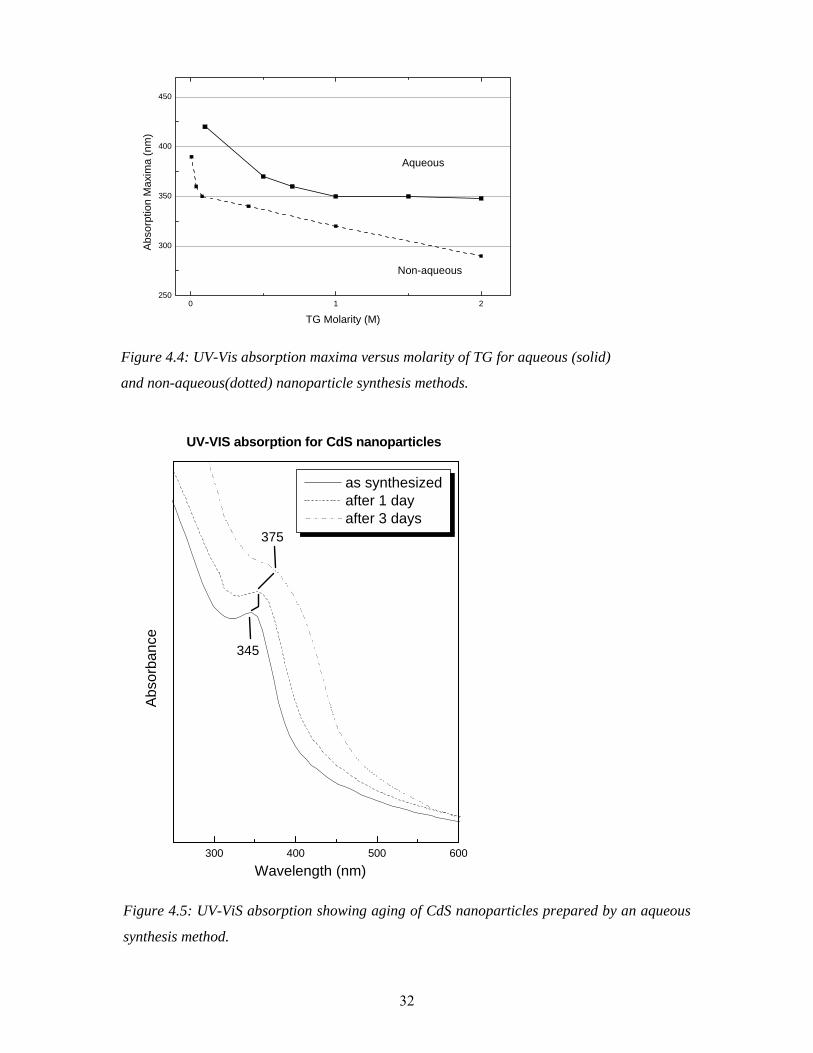
4.2.1 Aqueous and non aqueous methods The synthesis methods can be further classified as aqueous or non-aqueous synthesis depending upon the solvent used. The non-aqueous solvents can be ethanol, methanol, acetone, dimythleformamide (DMF), etc. The aqueous synthesis uses double distilled water as a solvent. The nanoparticles were synthesized with both techniques. The aqueous synthesis is comparatively less time consuming as the reactants are easily soluble in water, especially sodium sulfide. However the experiments show that there are some disadvantages of this technique in terms of reproducibility and growth. Also the aqueous synthesis has limitations in synthesizing smaller sizes. Figure 4.4 shows a plot of the position of UV-VIS absorption maxima (from which the size of the particle is determined) as a function of TG molarity. As mentioned before, differently sized particles can be synthesized by changing TG concentrations. In case of the aqueous synthesis (shown by the solid curve) there is no significant shift in the absorption maxima for molarities above 1.0. The absorption maxima are at 350 nm, which corresponds to a size of about 1.7 nm. In contrast, the non-aqueous synthesis (shown by the dotted curve) produces smaller particles above a TG concentration of 0.5 Molar. The absorption maxima shift to 290 nm (corresponding to particle size of about 1.1 nm) for a TG molarity of 2. Another important aspect regarding the choice of the method is aging of the particles. The particles tend to grow in an aqueous medium as it can be seen in figure 4.5. The absorption maximum shows a clear shift from 345 to 375 nm in 3 days for the particles produced in water. In contrast, the particles produced in ethanol show very high stability, as the absorption maximum shows hardly a shift within a period of about 6 months. Therefore the non-aqueous methods appear to be the better choice in the wet chemical synthesis for the particles under study. The increased synthesis time of the non-aqueous method is due to the poor solubility of cadmium acetate and sodium sulfide in ethanol. Note that, for the same concentration of TG, particles of different sizes are obtained from the aqueous and non-aqueous methods (see figure 4.4). Figure 4.6 shows UV-VIS absorption spectra of CdS nanoparticles synthesized by the non-aqueous method. The molarity of TG was varied from 2 to 10-3 M to get sizes from 1.3 nm to 4.2 nm. The sizes were determined using a Tight Binding Model (TBM) [10]. It can clearly be seen that, as the size of the particles decreases, the excitonic peak shifts to smaller wavelengths (blue shift) and shows an enhancement which is due to an increased oscillator strength (see chapter 2). Also the color of the particles changes from bulk like orange-yellow to white as shown by the pictures of the dried powders of the particles in the inset. 4.2.2 Monodispersity: Comparison of TG and MPA capping Large size distributions can give misleading results which have to be taken into account. A UV-VIS absorption spectrum with a distinct peak and sharp onset is an indication of a small size distribution. As mentioned earlier, there are a few reports showing highly monodispersed CdS nanoparticles. The goal of our efforts to improve the synthesis was to produce monodispersed particles and small sizes. Previously, in our laboratory, MPA was used for capping the nanoparticles (see, e.g., Winkler et. al [23]). However, a narrow size distribution and the accessibility of small sizes was questionable.
32
300 400 500 600
UV-VIS absorption for CdS nanoparticles
345
375
as synthesized after 1 day after 3 days
Abs
orba
nce
Wavelength (nm)
Figure 4.5: UV-ViS absorption showing aging of CdS nanoparticles prepared by an aqueous
synthesis method.
0 1 2250
300
350
400
450
Non-aqueous
Aqueous
Abs
orpt
ion
Max
ima
(nm
)
TG Molarity (M)
Figure 4.4: UV-Vis absorption maxima versus molarity of TG for aqueous (solid)
and non-aqueous(dotted) nanoparticle synthesis methods.
33
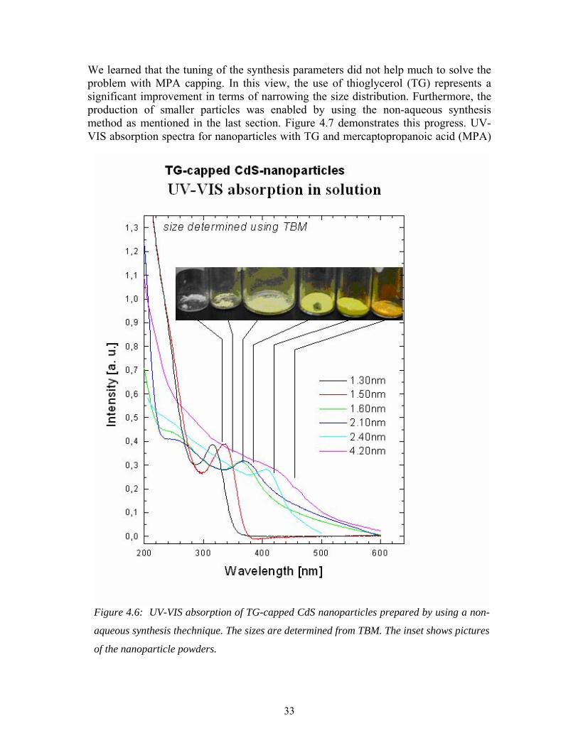
We learned that the tuning of the synthesis parameters did not help much to solve the problem with MPA capping. In this view, the use of thioglycerol (TG) represents a significant improvement in terms of narrowing the size distribution. Furthermore, the production of smaller particles was enabled by using the non-aqueous synthesis method as mentioned in the last section. Figure 4.7 demonstrates this progress. UV-VIS absorption spectra for nanoparticles with TG and mercaptopropanoic acid (MPA)
Figure 4.6: UV-VIS absorption of TG-capped CdS nanoparticles prepared by using a non-
aqueous synthesis thechnique. The sizes are determined from TBM. The inset shows pictures
of the nanoparticle powders.

34
capping molecules are shown. TG-capping results in a sharp onset and a prominent peak at 340 nm as compared to MPA-capping.
300 400 500 600
TG
MPA
Synthesized in Ethanol
340
UV-VIS absorptionfor CdS nanoparticles (~ 1.6 nm)
Abs
orba
nce
Wavelength (nm)
Figure 4.7: UV-VIS absorption spectra of CdS nanoparticles (d ~ 1.6 nm, TBM) prepared by
using TG and MPA capping.
4.2.3 Size-selective precipitation Size-selective precipitation of particles is a very powerful synthesis method for producing monodispersed particles. The method was adopted by the group of Weller; details can be found in Ref. [16]. This method was used here to synthesize our nanoparticles particularly in the view of narrowing the size distribution. Figure 4.8 shows a flowchart of the size-selective precipitation method for small CdS nanoparticles. This aqueous method uses cadmium perchlorate, sodium sulfide, and thioglycerol as the main reactants. 1.97 gms of Cd(ClO4) and 1 ml of thioglycerol were mixed with 250 ml of single distilled water in a three-necked reaction vessel and kept under stirring. Nitrogen gas was flushed from the reaction vessel in order to maintain an inert atmosphere.

35
Cd perchlorate + TG
in water Stir- 2hrs
pH adjusted to 11.2
with NaOH
Dialysis against water
Precipitation by addition of non solvent precipitate
Supernatent Precipitate
Figure 4.8: A flowchart for size selective precipitation of TG-capped CdS nanoparticles.
Add Na2S
300 400 500 600
UV-VIS absorption for CdS nanoparticles
320
290260
mixture supernatant precipitate
Abso
rban
ce
Wavelength (nm)
Figure 4.9: Size selective precipitation of CdS nanoparticles immediately after the synthesis.
UV-VIS absorption spectra of the mixture as synthesized (solid curve), the supernatant
(dashed curve), and the precipitate (dotted curve) after the first precipitation are shown.

36
After 2 hours of vigorous stirring a 1 molar solution of NaOH is added to adjust the pH of the mixture to 11.2. This is followed by addition of 1.12 mM (25 ml) of Na2S and stirring for 2 hours. The transparent mixture is filtered with dialysis against water for several hours. This mixture is then size-selectively precipitated by drop wise addition of ethanol and simultaneous stirring. The bigger particles in the mixture start precipitating after addition of few tens of milliliters of ethanol. The stirring is continued further to assist the precipitation. The precipitate is separated by centrifugation. The left-over solution, i.e., the supernatant, is again re-precipitated by the addition of ethanol, and this step is repeated in order to separate out the remaining bigger particles in the supernatant. Thus the supernatant consists of a solution of smaller particles only. Similarly, the precipitate is refined by re-precipitation with ethanol. Figure 4.9 shows UV-VIS absorption spectra of as-synthesized solution (mixture), supernatant, and precipitate after the first precipitation by addition of ethanol. The mixture is precipitated immediately after the synthesis (without the dialysis). It can be seen that the precipitation of particles of bigger size (absorption at 320 nm) takes place and that the supernatant has contributions of smaller particles (absorption at 260 nm and 290 nm). The mixture treated with dialysis is free of the sizes below 300 nm but only after a long dialysis time, i.e., 43 hours. A very short description of the dialysis
300 400 500 600
Supernatant
Precipitate
Mixture
UV-VIS absorption for CdS nanoparticles
355
325
Abso
rban
ce
Wavelength (nm)
Figure 4.10: CdS nanoparticles prepared by size selective precipitation. UV-VIS absorption
spectra of the mixture (solid curve), supernatant (dashed curve), and precipitate (dotted
curve) are shown.

37
method is given below. This method was used before for ZnS particles by our collaborators in Pune. Dialysis is a filtration method, in which a nonreactive porous membrane (dialysis bag) is used as a filter. The dialysis bag is filled with the particle solution and immersed in a water bath. Due to the concentration gradient between the solution in the bag and the water outside of the bag, only those particles with sizes smaller than the pores of the membrane can flow out of the bag. The bigger particles stay inside the bag and thus get separated. To maintain a concentration gradient, fresh water is added continuously to the water bath. The dialysis has to be carried out for several hours in order to completely get rid of the smaller particles. Figure 4.10 shows UV-VIS absorption spectra for a mixture for which dialysis was carried out for 43 hours (solid curve), supernatant (dashed curve) and precipitate (dotted curve) after the first precipitation. The mixture mainly shows particles with 325 nm absorption. The precipitate shows a nice absorption peak at 355 nm, and the supernatant shows an absorption peak at 325 nm similar to the mixture. This is because there are only few particles showing an absorption peak at 355 nm in the mixture (this can be seen from the weak signal of the precipitate), and the precipitation of these particles hardly changes the contributions of the mixture. The size distribution is significantly improved by this method. However, the reproducibility was insufficient due to the aqueous medium. Furthermore, the re-precipitation step in this method was not very successful in refinement of the precipitate and of the supernatant.
4.3 Thin film preparation After the preparation of the nanoparticles they were stored as free standing powders. These powders can be used directly as samples for characterizations such as
photoluminescense (PL), x-ray diffraction (XRD), micro-Raman, etc. to study the bulk properties. However a uniform and relatively thin film of the nanoparticles is needed for photoemission measurements. This is to generate a good signal and to minimize charging effects of the sample. The sample can also be obtained by pressing the nanoparticle powder into a soft metal foil, Indium. However, this kind of sample shows some charging due to larger thicknesses in a nonuniform film. Thin films were prepared for the photoemission experiments presented in this thesis mainly by a drop deposition technique. The nanoparticle powders were
Figure 4.11: AFM image of CdS nanoparticles, d =
1.35 nm (from TBM), deposited on Au-coated silica by
an electrophoresis technique.

38
dissolved in double distilled water or ethanol for the deposition. A drop of the nanoparticle solution was then deposited on a Au-coated SiO2 substrate and kept under an infrared lamp to facilitate the evaporation of the solvent. The substrate was cleaned before deposition with acetone using an ultrasonic cleaning bath. In order to study the effects of different film preparation techniques, films were also prepared using an electrophoresis technique. In the electrophoresis technique a negatively charged solution of nanoparticles was placed between two electrodes with the sample as anode, and then a voltage was applied. In this way a controlled amount of particles was deposited on a cleaned, Au-coated silica wafer. The morphology of the deposited film is strongly influenced by parameters such as the concentration of the solution, the pH value, and the voltage. Figure 4.11 shows an AFM image of an electrophoresis film of CdS nanoparticles (CdS-E, d ~ 1.35 nm, see chapter 5). The light spots represent the deposited particles while the dark areas stem from the substrate. AFM images taken on different spots of the sample look similar. It can be seen that very thin (~ 40 nm) and uniform deposition is possible with electrophoresis. However, there is an indication of agglomeration of the particles on the substrate, since the white spots are as large as about 50 nm. It is noted that the quality of the film depends on the solubility of the powders in the solvent. For larger sizes, the powders are hard to dissolve and the films are not uniform. For this reason, a freshly prepared nanoparticle solution was always used to prepare films for photoemission experiments. These reveal that the films prepared from freshly synthesized nanoparticle solutions are of better quality as less substrate is exposed and as the films are homogeneous, as discussed in Chapter 7.

39
Chapter 5
High-resolution photoemission study of CdS nanoparticles This chapter focuses on a detailed analysis of the XPS spectra of very small, TG-stabilized CdS nanoparticles with improved size distribution (see Chapter 4). The XPS spectra for glutathion-capped nanoparticles (1.8 nm) will also be discussed for a comparison of different capping. This chapter also presents a new approach for the analysis of photoemission spectra of CdS nanoparticles and highlights spectral differences in the photoemission spectra as a function of size and capping. The synchrotron radiation (SR) high-resolution photoemission data will be introduced in section 5.1. The high-resolution photoemission signals of such nanoparticles consist of different S components as will be shown from a quantitative data analysis. In section 5.2, an assignment of spectral sulphur components will be presented. The assignment will be done on the basis of the spectral changes as a function of photon energy and beam exposure time. The beam exposure results will be discussed in this chapter for the purpose of assignment and more information is given in Chapter 7, section 2 (effect of beam damage). As will be discussed, a calculation of the photoemission intensity based on a structural model and a comparison with the experimental data is quite helpful to understand the spectral changes and to assign the different S components. Section 5.3 introduces initial photoemission calculations and data comparisons for 3 different models (computed “manually” to see the trends as a function of surface sensitivity and beam exposure). The results of this model comparison show some interesting features of the photoemission data analysis, which allow an indirect estimate of the size of the particle. To check various parameters involved in the calculations and to avoid errors, a computer program was written by Lothar Weinhardt and Oliver Fuchs to perform (orientation-averaged) calculations. Before discussing the program, section 5.4 gives a short overview of the determination of the inelastic mean free path, λ. Furthermore, for our experimental photon energies, λ values are estimated. Section 5.5 then presents a discussion of the development of the above-mentioned program to calculate photoemission intensities and discusses plausibility checks for the code. The application of this program to a few structural models will be presented at the end of the chapter. It will be seen that the program confirms the manual calculation results, and offers a way to estimate the size of CdS-B in the present case. Furthermore, it can be seen that the value of λ in the program does not affect the results significantly, as checked with four different values of the λ. Moreover, the effect of the shape is also checked by the calculations. The results hint towards a more or less spherical particle shape of CdS-B. The results of this study are exciting but there is a need to check more models with the program in order to derive concrete conclusions from this new approach of photoemission analysis, which is in process. 5. 1 Results: Differently sized particles look very different Figure 5.1 shows UV-VIS absorption spectra of three differently sized nanoparticles, CdS-A, CdS-B, and CdS-C. As expected [6, 9], the spectra are very different compared to the absorption of bulk CdS. In particular a shift of the absorption edge

40
from 515 nm towards smaller wavelengths (higher energy) is observed with decreasing crystallite size. CdS-A and CdS-B show a sharp peak, positioned at 290 nm and 318 nm, respectively, while CdS-C shows a broader peak at 370 nm. This peak broadening observed for
bigger particles can be attributed to the size-dependant oscillator strength, as discussed in Chapter 2. The observed sharp onset and the distinct “exciton” peaks are indications of a narrow size distribution of the nanoparticles, in particular for CdS-A and CdS-B. The band gaps calculated from the absorption peak are 4.31 eV, 3.90 eV, and 3.52 eV (with error bars of ±0.1 eV), for CdS-A, CdS-B, and CdS-C, respectively. A tight binding model is used to estimate the particle sizes from these band gap energies [10]. This gives diameters of 1.1 (±0.1) nm, 1.4 (±0.1) nm, and 1.75 (±0.1) nm for CdS-A, CdS-B, and CdS-C, respectively. An x-ray diffraction analysis of two similar nanoparticles (with the same absorption positions as CdS-B and CdS-C) shows broadened peaks (compared to the CdS bulk reference, as expected) and reveals a
wurtzite structure [50]. Using the Debye-Scherrer formula and assuming a spherical shape, the diameter of the particles can be estimated. Following a new approach, in which XRD patterns for nanoparticles with different sizes are calculated and compared to the experimental data [50], we find sizes of 1.4 ± 0.35 nm (CdS-B) and 1.7 ± 0.25 nm (CdS-C), which is in good agreement with the results obtained from optical data in comparison with tight binding calculations. Furthermore, the XRD-approach also determines the number of atoms in the particle (which contribute to the coherent scattering process), which is an important information for the interpretation of our photoemission data. High-resolution photoemission spectra of the S 2p core levels for CdS-A, CdS-B, CdS-C, and CdS-D are shown in Figures 2 (a), (b), (c), and (d). Note that CdS-A, CdS-B, and CdS-C are TG-capped nanopatricles whereas CdS-D is a glutathione-capped nanoparticle. Two photon energies (254 eV and 720 eV) were employed to maximise or reduce the surface sensitivity, respectively. Also, the residua, i.e., the differences
Figure 5.1 : UV-VIS optical absorption spectra of CdS-A (d ~ 1.1nm), CdS-B (d ~ 1.4 nm), and CdS-C (d ~ 1.75 nm) nanoparticles.

41
between the data and the fit, are shown on a magnified scale (factor 2). Earlier high-resolution photoemission experiments (at BESSY I) on CdS nanoparticles (2.4 nm - 7 nm) with mercaptopropanic acid (MPA) as a stabilizer show three to four different species of sulfur atoms and reveal their contribution as a function of size [23]. At that time, the spectra were recorded for several minutes without any apparent production of beam-induced changes. In the current study, we investigate smaller clusters (1.1 – 1.75 nm) with a narrow size distribution (15 - 20 %), which is partly due to the different capping agent (TG). Such smaller particles have a larger ratio of surface to bulk, which facilitates the spectral separation of the different components. Furthermore, the undulator beamline UE 52–PGM at BESSY II (a third generation synchrotron radiation source) delivers much higher photon flux and hence allows to quickly take spectra with high spectral resolution. It was important to check beam damage effects for these nanoparticles due to the different capping and, in particular, the higher excitation flux. In order to study and avoid beam-induced effects (see below), the spectra of Fig. 2 were taken within one minute and repeated many times (not shown here, see discussion in Chapter 7). In spite of the short accumulation time, the signal to noise ratio is quite good. Note that the spectra shown here are from the center of the dried nanoparticle drop on the sample, and that there are some spectral changes at the rim of the drop, as will also be discussed in Chapter 7. The data evaluation was done by fitting the S 2p spectra individually and, for selected spectra, also simultaneously to check the consistency of the fits. The spectra were fitted with the smallest possible number of peaks (spin-orbit split doublets) using Voigt functions and assuming equal (optimized) line widths for all S components. The spin-orbit splitting of the S 2p1/2 - S 2p3/2 doublets was fixed at 1.2 eV with a peak area ratio of 1:2. The binding energy positions and the Gaussian and Lorentzian widths were included as free parameters. A linear background was simultaneously fitted with the peaks. The residuum, i.e., the difference between the data and the fit, was plotted in each case to check the quality of the fit and the statistical nature of the fitting deviations. The spectra look quite different from each other for the four particles under investigations. A closer look at the spectral changes with the size of the particle shows a drop in the intensity of low binding energy contributions with size, which represent peaks associated with sulfur atoms in the bulk of the particle. This is consistent with the earlier results for MPA-capped particles [23]; in contrast, however the fits clearly indicate five sulfur species in the present (TG-capped) particles. If the spectra are fitted with less than five Voigt-lineshape doublets, the fits show significant deviations from the data. As mentioned above, a variation of the photon energy can be used to vary the kinetic energy and hence the inelastic mean free path of the emitted photoelectrons and thus the surface sensitivity. It is maximised by tuning the photon energy to 254 eV (corresponding to a kinetic energy of about 92 eV, yielding a mean free path of about 0.5 nm, see [21] and section 4). Hence peaks the relative intensity of which increases when changing the photon energy from 720 to 254 eV are associated with near-surface species. The different sulfur species within these nanoparticles in the binding energy range from 160 eV to 167 eV may be located quite differently and are quite sensitive to a small change in the particle size. A simple picture considering the particle as a sphere is not helpful and a better understanding of the particle structure is

42
Figure 5.2: X-ray photoemission spectra of S 2p core levels for (a) CdS-A (d ~ 1.1 nm), (b)
CdS-B (d ~ 1.4 nm), (c) CdS-C (d ~ 1.75 nm, and (d) CdS-D (d ~ 1.8 nm). CdS-D is
glutathion-capped and CdS-A through –C are TG-capped. The spectra were recorded with
photon energies of 720 eV and 254 eV for each sample. The fit reveals five S 2p doublets (I-V,
solid lines), which are identified as different sulfur components as described in the text. The
residuals (i.e., the difference between the data and the fit) are shown below the corresponding
spectra on an enlarged scale.

43
mandatory. The different S components are labeled I (161.35 eV ± 0.07 eV), II (162.10 eV ± 0.07 eV), III (163.00 eV ± 0.05 eV), IV (163.80 eV ± 0.07 eV), and V (164.50 eV ± 0.05 eV). For the TG stabilized particles (a), (b), and (c), the intensity variation of the sulfur components I - V with photon energy shows differences form particle to particle. The particles with similar size but different capping, (c) and (d), show differences in the intensity of components I – V even for the bulk sensitive photon energy of 720 eV. In this case it is not possible to come up with a single component assignment for all the particles. So the five sulfur species within these nanoparticles may be located quite differently, and their location is quite sensitive to a small change in the particle size. Alternatively, to understand the intensity distribution and variation of the sulfur components I - V, it is quite helpful to know the actual number of S atoms in the core and on the surface of the particles as well as their chemical environment (e.g., number of Cd bonds) around each S species. This information can in parts be obtained from XRD, and thus it is possible to assign the components I to V to different sulfur species in the particles, as will be shown in the next section.
5. 2 Assignment of spectral sulfur components The particles show intensity variation of the sulfur components when the photon energy is tuned (section 5.1). This effect is now used to identify surface-near species. Differences are found for both, different particle sizes and different capping agents. The reason for this could be different locations of the sulfur species in each kind of particle. We can additionally take changes in the S components into account, which are caused by long beam exposure. To study the beam damage, S 2p photoemission spectra for CdS-A, CdS-B, and CdS-D were collected successively for 12 minutes with a beam exposure of about 1 minute per scan (Chapter 7, Fig. 7.3). The beam exposures were considered to induce dissociation and desorption of organic capping molecules [66], which will help us to assign the S component which represents the capping agents. We will try to assign the components for CdS-B first, because we have more insight into the structural aspects of this particle, and then we shall use these results for CdS-A. In order to highlight the intensity changes of the sulfur components with photon energy and beam exposure, bar graphs are plotted for CdS-A and CdS-B as shown in Figure 5.3 (a) and (b), respectively. The black bars, gray bars, and cross-hatched bars represent the fraction of total S 2p intensity at photon energies of 720 eV, 254 eV, and after a beam exposure of 12 minutes at 254 eV, respectively. The error margins of the fits are marked on each bar in the figure. For CdS-B, we first analyze the effect of photon energy variation. For the surface sensitive photon energy (254 eV), components III - V show a rise in relative intensity and are thus associated with surface-near species, while components I and II show a reduction at 254 eV and are thus associated with bulk species (e.g., S atoms in a four-fold Cd atom coordination). The binding energy positions of these components tell us about the surrounding chemical environment. Final state effects such as poor screening (e.g., at the surface) result in a shift to higher binding energy. We can say that S atoms experience a decreasing coordinative environment going from component I to component V, to be consistent with the previous reports on CdS nanoparticles [23, 45]. Thus, component I represents S atoms with 4 Cd neighbours and component II
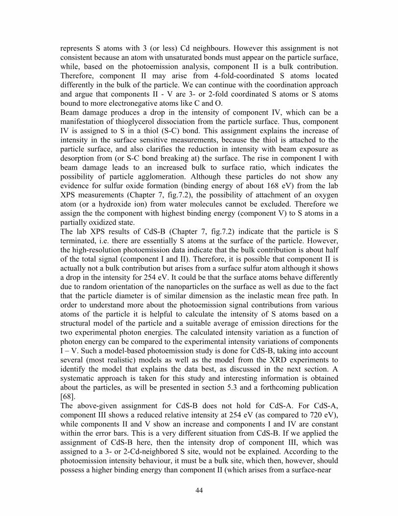
44
represents S atoms with 3 (or less) Cd neighbours. However this assignment is not consistent because an atom with unsaturated bonds must appear on the particle surface, while, based on the photoemission analysis, component II is a bulk contribution. Therefore, component II may arise from 4-fold-coordinated S atoms located differently in the bulk of the particle. We can continue with the coordination approach and argue that components II - V are 3- or 2-fold coordinated S atoms or S atoms bound to more electronegative atoms like C and O. Beam damage produces a drop in the intensity of component IV, which can be a manifestation of thioglycerol dissociation from the particle surface. Thus, component IV is assigned to S in a thiol (S-C) bond. This assignment explains the increase of intensity in the surface sensitive measurements, because the thiol is attached to the particle surface, and also clarifies the reduction in intensity with beam exposure as desorption from (or S-C bond breaking at) the surface. The rise in component I with beam damage leads to an increased bulk to surface ratio, which indicates the possibility of particle agglomeration. Although these particles do not show any evidence for sulfur oxide formation (binding energy of about 168 eV) from the lab XPS measurements (Chapter 7, fig.7.2), the possibility of attachment of an oxygen atom (or a hydroxide ion) from water molecules cannot be excluded. Therefore we assign the the component with highest binding energy (component V) to S atoms in a partially oxidized state. The lab XPS results of CdS-B (Chapter 7, fig.7.2) indicate that the particle is S terminated, i.e. there are essentially S atoms at the surface of the particle. However, the high-resolution photoemission data indicate that the bulk contribution is about half of the total signal (component I and II). Therefore, it is possible that component II is actually not a bulk contribution but arises from a surface sulfur atom although it shows a drop in the intensity for 254 eV. It could be that the surface atoms behave differently due to random orientation of the nanoparticles on the surface as well as due to the fact that the particle diameter is of similar dimension as the inelastic mean free path. In order to understand more about the photoemission signal contributions from various atoms of the particle it is helpful to calculate the intensity of S atoms based on a structural model of the particle and a suitable average of emission directions for the two experimental photon energies. The calculated intensity variation as a function of photon energy can be compared to the experimental intensity variations of components I – V. Such a model-based photoemission study is done for CdS-B, taking into account several (most realistic) models as well as the model from the XRD experiments to identify the model that explains the data best, as discussed in the next section. A systematic approach is taken for this study and interesting information is obtained about the particles, as will be presented in section 5.3 and a forthcoming publication [68]. The above-given assignment for CdS-B does not hold for CdS-A. For CdS-A, component III shows a reduced relative intensity at 254 eV (as compared to 720 eV), while components II and V show an increase and components I and IV are constant within the error bars. This is a very different situation from CdS-B. If we applied the assignment of CdS-B here, then the intensity drop of component III, which was assigned to a 3- or 2-Cd-neighbored S site, would not be explained. According to the photoemission intensity behaviour, it must be a bulk site, which then, however, should possess a higher binding energy than component II (which arises from a surface-near

45
sulfur species). The beam damage analysis shows, in contrast to CdS-B, a rise of components II and IV, and a drop of component III. To understand these changes it is necessary to analyze CdS-A entirely independently from CdS-B. Due to the very small particle sizes, the electronic structure (in particular of CdS-A) becomes more and more influenced by molecular effects, and hence the photoemission spectra of these particles can be very different from the others. Furthermore, we can think of a very different behavior of the particles under beam exposure. For example, the rise in component IV (“thiol” or, more precisely, the S-C bond) could be due to a fragmentation of the
0.0
0.1
0.2
0.3
0.4
0.5
0.6
0.7
VIII IVIII
(a) CdS-A (d ~ 1.1 nm)
720 eV 254 eV beam exposure
for 12 min at 254 eV
Frac
tion
of S
2p
inte
nsity
0,00
0,05
0,10
0,15
0,20
0,25
0,30
0,35
0,40
VIVIIIIII
Frac
tion
of S
2p
inte
nsity
(b) CdS-B (d ~ 1.4 nm)
720 eV 254 eV beam exposure
for 12 min at 254 eV
Figure 5.3: Bar graph plots of the intensity distributions and variations of the different S-
components as a function of photon energy and beam exposure, for experimental data of CdS-A
(d ~ 1.1 nm) (a), and CdS-B (d ~ 1.4 nm) (b). Beam induced changes after an exposure time of
12 minutes are shown by cross-hatched bars. Black and light gray bars represent photon
energies of 720 eV and 254 eV, respectively. In each case the ordinate shows the fraction of the
total S 2p intensity.

46
capping molecule under the beam, giving rise to additional of S-C (e.g. S-CH2, S-CH etc.) bonds. Moreover, Cd-S bonds at the surface might be broken, indicating a drop of component III (S atoms with 3 Cd neighbors) and a rise of component II (S atom with 2 Cd neighbors). In order to confirm and quantify this assignment, there is a need to gain more structural insight into the CdS-A particle. As will be shown for CdS-B in the following section, this can be achieved by a detailed, model-based intensity analysis. However, this analysis requires XRD data as starting parameters, and since no XRD data is yet available for CdS-A at this point, a model-based analysis is not attempted at present. 5.3 Model-based photoemission intensity calculations for CdS-B As mentioned before, in the XRD-approach developed by C. Kumpf et al., the experimental XRD data is compared to simulated XRD patterns for a range of particle sizes. From a wurtzite CdS structure of individual particles with diameters between 1 nm and 10 nm, XRD patterns are computed with a computer program as follows. Depending on the particle diameter, the program chooses the number of unit cells and removes all atoms which are located beyond the experimentally determined radius. Then the XRD pattern is calculated for these structures and fitted to the experimental data. Note that the patterns only represent the coherent core of the particles and in particular do not incorporate the sulfur atoms from the capping molecules. Structures with diameters of 1.38 nm and 1.72 nm fit best to experimental data of CdS-B, from which we derive the approximate particle size (1.5 ± 0.2 nm) and the number of Cd and S atoms (26 and 44, respectively). From this information, two simple ball-stick models (models 1 and 2) were built for the coherent core of CdS-B, one with 52 atoms (26 each, of S and Cd) and one with 88 atoms (44 each of S and Cd). Figure 5.4 depicts the models with 26 S atoms (Model 1, a) and 44 S atoms (Model 2, b). In addition, Model 3 (Fig. 5.4 (c)) was built from a proposed structure of 1.4 nm diameter CdS nanoparticles as reported by Döllefeld et al. [69]. Of course, it is possible to build many models for CdS-B with wurtzite structure and 26 - 44 atoms of S and Cd, but we concentrate on the three models above: Models 1 and 2 represent the best-fit XRD structures (of diameters 1.38 nm and 1.72 nm), and Model 3 represents a structure derived by Vossmeyer et al. [47] from single crystal XRD for a 1.4 nm particle. For the assignment of S-components, a systematic comparison of the experimental photoemission intensity variations of components I - V to the calculated intensity variations of S atoms from these models was undertaken. Here, we focus only on CdS-B, because it has about 1/3 of the number of atoms as compared to CdS-C and CdS-D and a very narrow size distribution. As mentioned above, XRD data of CdS-A is not available and hence we do not attempt a model-study of these particles in this thesis. The intensities of S atoms with different Cd neighbors are calculated from the models taking into account an exponential relationship between intensity (I), the layer thickness “above” the emitting atom (d), and the inelastic mean free path (λ):
I = I0e(-d/λ)
Considering one orientation of the particle, e.g., looking at the (001) plane from the top, the intensities are calculated for all S atoms within the particle (with varying ‘d’

47
from top to bottom) for the photon energies of 720 eV and 254 eV. Then, the intensities are summed up for all S atoms of the same class (with the same number of Cd neighbors), and the intensity fraction of each such class (i.e. with 1, 2, 3, or 4 Cd neighbors) is calculated. All this is done for 10 different orientations of the particle and the intensities are averaged assuming equal contributions from each orientation (i.e., a random orientation of the nanoparticles on the substrate). With these calculations we approximate the real intensity contribution for each class of S atoms and its variation with photon energy. In these calculations, we have used the inelastic mean free path (λ) values determined from the plot of mean free path data of electrons given in Ref. [21]. The inelastic mean free path values for the photon energies 720 eV and 254 eV are 10 Å and 7 Å, respectively. Note that the “universal curve” only gives a crude approximation of the inelastic mean free path, as will be discussed in more detail in section 5.4. For the present calculations (10 orientations, “manual” intensity evaluation), which are intended to detect trends in the photoemission intensity behavior, the such-determined values are sufficient. For the complete, program-based approach in section 5.5, refined values will be used (which are computed in section 5.4).
(a) Model 1 (b) Model 2 (c) Model 3
Figure 5.4: Schematic “ball and stick” models for CdS-B nanoparticles: with 26 (Model 1, a)
and 44 S atoms (Model 2, b), and a proposed model from literature (Model 3, c) [69]. For
Models 1 and 2, the small cyan circles represent Cd atoms, while the big yellow circles
represent S atoms. For Model 3, the small black circles represent Cd atoms and the white and
dark-gray circles represent S atoms. Also, S components with different Cd neighbors are
shown in the models. S atoms in a thiol bond are shown for Model 1 with dark hollow circles
on top of the Cd-terminated plane.
The non-polar surface Cd atoms have only one open bond (surrounded by three S atoms) and hence could provide a comparatively less attractive site for the S atom of thiol. Similarly, oxygen or hydroxyl atoms may not bind to S atoms of non-polar planes but rather attach to the S atoms from the bottom plane (S-terminated). On this basis, we modify our models 1 and 2 by attaching thiol S atoms at Cd atoms on the top
S atom with 4 Cd neighbors
S atom with 3 Cd neighbors
S atom with 2 Cd neighbors S atom with 1 Cd
neighbor S from Thiol

48
(Cd terminated) plane. These thiol atoms are shown in Figure 5.4 for model 1 (a) by dark hollow spheres. Now, model 1 has 33 S atoms (26 plus 7 S-thiol atoms) and model 2 has 51 S atoms (44 plus 7 S-thiol atoms). Thus, models 1 and 2 have become S-terminated models for CdS-B. This is consistent with the lab XPS data (Chapter 7), which indicates a S-termination of the particles based on normalized intensity ratios of the S and Cd peaks. The attachment of oxygen to the 2-Cd-neighbored site is also considered for the three models. Consequently, we have S atoms with five different chemical environments for models 1and 2, i.e., S atoms with 4 Cd bonds (4 Cd neighbors) in the core, S atoms with 3 Cd bonds and 2 Cd bonds on the surface, S atoms from thiol (bound to 1 Cd atom), and S atoms attached to oxygen (bound to 2 Cd atoms). For model 3 we have to have five chemical environments in order to compare with the five components of the experimental data. Model 3, however, does
0.0
0.1
0.2
0.3
0.4
720 eV 254 eV beam exposure of
12 min at 254 eV
Frac
tion
of S
2p
inte
nsity
Frac
tion
of S
2p
inte
nsity
Frac
tion
of S
2p
inte
nsity
(a) Experimental data
Frac
tion
of S
2p
inte
nsity
0.0
0.1
0.2
0.3
(b) Model 1
0.0
0.1
0.2
0.3
S-oxide4 Cd neighbors
(c) Model 2
0.0
0.1
0.2
0.3
Thiol-1 Cd neighbours
Thiol-1/2 of2 Cd neighbors
S-oxide
1 Cd neighbors
2 Cd neighbors
2 Cd neighbors
3 Cd neighbors
4 Cd neighbors
Thiol-1 Cd neighbours
2 Cd neighbors
S-oxide3 Cd neighbors
4 Cd neighbors
VIVIIIIII
(d) Model 3
Figure 5.5: Bar graph plots for the intensity contributions and variations of the different S-
components as a function of photon energy, for experimental data (a), model 1 (b), model 2 (c),
and model 3 (d)( for the models see figure 5.4). Beam induced changes after an exposure time
of 5 minutes are shown in (a) by hatched bars. Black bars and light gray bars represent photon
energies of 720 eV and 254 eV, respectively. In each case the ordinate shows the fraction of the
total S 2p intensity.

49
not have S atoms with 3 Cd neighbors. Therefore we consider the 3 corner S atoms with 1 Cd neighbor as a distinct S species and assume that thiol atoms bind to half of the 2-Cd-neighbored S atoms, thus leading to five different chemical environments. Furthermore, we assume here that there is no difference in binding energy positions of thiol when attached to 2 or 1 Cd atoms, because the Cd environment will have much less influence than the strong covalent bonding of C towards the S atom in the S-C bond of this organic molecule. With this we continue further with the comparison of the photoemission intensities of the five different species in the models with five different S components in the experimental data. For a better comparison of the results, bar graphs are plotted for the experimental data (Figure 5.5, a) and the calculations (Figure 5.5, b-d). Figure 5.5 (a) is reproduced from Section 5.2 (error bars are not shown here). Figure 5.5 (b), (c), and (d) show bar graphs for three models. The experimental data shows an intensity drop for 2 components and a rise for 3 components when the photon energy is varied from 720 eV to 254 eV (black and light gray bars, respectively). Any valid model should at least predict the correct number of sulfur sites showing an intensity drop or rise for the surface sensitive measurement. In this respect, Model 1 (Figure 5.4, b) shows an intensity drop for 2 sulfur species and a rise for 3 sulfur species, which leads to a total of 12 possible peak assignments (2! 3! = 12). Models 2 and 3 fail to reproduce the experimental data, because there is drop in intensity for one sulfur site only (4-Cd-neighbors) in case of Model 2 and because the intensities are almost constant for Model 3. In case of model 1, the number of possible peak assignments can be reduced by taking the beam-induced intensity variations at 254 eV into account (see Figure 5.4 (a) - hatched bars). As done before, the intensity reduction of component IV can be assigned to an intensity drop of the thiol species, which leaves us only with 4 peak assignments in total (see table 5.1). As discussed above, the breaking of thiol bonds may establish new S-Cd bonds and hence may lead to agglomeration. Thus there is a rise in the 3-Cd or 4-Cd-neighbored sites and hence an increase of component I. Taking the binding energy positions of the components into account, we obtain peak assignment (1), which is consistent with earlier reported typical surface core level shifts for II-VI semiconductor surfaces [70, 71] and with previous work on CdS nanoparticles [23, 45]. Note that the present analysis is made to test the models in view of the photoemission data and find out the possible peak assignment from the models, initially without taking the binding energy positions and beam damage effect into account. The idea was to determine the model that gives the best explanation for the photoemission data of the CdS-B particles. Here we suggest that CdS-B most likely has the structure of model 1. As model 2 fails to explain the photoemission data, we end up with the interesting conclusion that our model-based interpretation of the photoemission data results in information about the size of CdS-B. CdS-B apparently is smaller than 1.7 nm, i.e. 54 S atoms, represented by model 2. It probably has about 33 S atoms, corresponding to a diameter of 1.4 nm. The present (manual) calculations were performed in order to understand the trends in the intensity differences. However, in order to improve the arguments, a suitable computer program to perform proper calculations with full 3-dimensional averaging is necessary. The program also allows to check important points in the intensity calculation, e.g., what is the effect of of the

50
particle shape, the termination and the influence of variations in the value of the inelastic mean free path on the intensities of different S species. We can thus use various λ values and try different models for CdS-B, which will give further insight into the results of the comparative study. We have tried to minimize the error in the determination of the λ values for our experimental energies using appropriate equations developed by Seah, Powell et al., as mentioned before; details are given in the next section.
Table 5.1: Possible peak assignments based on intensity variations. The changes due to the
surface sensitive measurement and to radiation damage effects are already taken in to
account to reduce the number of possible peak assignments.
5.4 Inelastic Mean Free Path (IMFP) of electrons
As mentioned in the experimental section, the small IMFPs of photoelectrons make photoemission a surface sensitive technique. The IMFP (λm) is a measure of the average distance travelled by an electron through a solid before it is inelastically scattered [21]. It is dependent upon the initial kinetic energy of the electron and the nature of the solid. The photoelectron also undergoes elastic scattering processes, which reduce the attenuation length, which is the distance after which the fraction 1/e of the electrons arrives without energy loss. The attenuation length (AL) is equal to the IMFP in the absence of elastic scattering.
The major contribution in this field has been given by Seah et al. and Powell et al. [72-83]. They have put extensive efforts in understanding the physics behind the IMFP and presented a set of equations which can be used for calculations for the system of interest. Seah and Dench [72] presented a compilation of measurements of λ for different solids in the kinetic energy range between 0 eV and 10 keV. This documentation is of significance as it gives rise to the so-called universal curve, which is referred to thereafter for the determination of the IMFP. Their analysis of λ provides a set of relationships for elements, inorganic compounds, and organic compounds over a wider energy range where λ follows an E0.5 dependence. Wagner et al. found that the energy dependence of λ is rather Em, where m varies between 0.54 - 0.81. Tanuma et al. [73-77] presented calculations of the IMFP for the energy range of 50-2000 eV for a large number of elements and compounds. The calculated IMFP values were fitted to a modified form of the Bethe equation for inelastic scattering in matter. They found
Component I Component II Component III Component IV Component V
(1) 4 Cd neighbors 3 Cd neighbors 2 Cd neighbors Thiol S-Oxide
(2) 4 Cd neighbors 3 Cd neighbors S-Oxide Thiol 3 Cd neighbors
(3) 3 Cd neighbors 4 Cd neighbors 2 Cd neighbors Thiol S-Oxide
(4) 3 Cd neighbors 4 Cd neighbors S-Oxide Thiol 3 Cd neighbors

51
that the parameters in this equation can be related to the material parameters such as atomic or molecular weight, density, and the number of valence electrons per atom or molecule. The resulting equation is referred to as the TPP-2 formula [79]. The TPP-2 equation for the IMFP, as a function of electron energy, E (in eV), is
where Ep = 28.8 (Nvρ/M)1/2 is the free-electron plasmon energy (in eV), Nv is the number of valence electrons per atom (for elemental solids) or molecule (for compounds), ρ is the density (in g/cc), M is the atomic or molecular weight, and Eg is the band gap energy (in eV). Very recently Tanuma et. al. reported on a comparison of IMPF values calculated by the TPP-2 equation using Nν values recommended by them and by Seah [81] with calculated reference optical data for 8 elements and two compounds [82]. They recommend the use of Nν values given by them because of smaller RMS deviations. A simple equation for calculating overlayer thicknesses in which IMPF can be substituted was recently studied by Seah et al. [83]. They found that a more accurate standard quantification can be achieved by substituting IMFP by AL. This is because the standard equation neglects a number of secondary effects mainly elastic scattering apart from the simple inelastic loss. They used an accurate Monte-Carlo simulation for electron transport in a overlayer and considered, how AL values can be chosen specifically to minimize the errors in overlayer quantification. They provided AL values for the elements studied by Tanuma et. al. and developed a semiempirical equation that fits these AL values with much less uncertainty. These equations are simple enough to apply to any compound. A modified equation for the calculation of AL is referred to as the CS 2 equation (the equation is modified by including an electronic structural quantity, i.e., lattice parameters). It is given by
where E is the electron energy in eV, a is the lattice parameter of the compound in nm, and Z is the atomic number of the compound. The idea behind this overview was to generate a feeling for the IMFP determination as we would like to choose the best value of the IMFP for the kinetic energies used in the photoemission experiments of our CdS nanoparticles. It can be seen that there is a

52
large error bar in the determination of λ from the universal curve for a specific element of interest. The error bars come from the different results of λ for different solids and become even larger for a specific solid when a different set of experiments is done. Therefore it is in general not a good choice to use such universal curves for determining the IMPF. We instead use the equations as given above. We use CdS bulk parameters such as the density (4.8 g/cc), the compound weight (144.7 g/cc), number of valence electrons (18), and the lattice parameter (4.5 Å), and calculate λ values from the two equations as mentioned above, i.e., from the TPP-2 and the CS 2 equation. The calculated values are given below in Table 2. The λ values are calculated using CdS bulk parameters (see above), and there is certainly a difference in the attenuation for the nanoparticles. However, we have little information about the nanoparticles. Especially the parameters necessary in the equations such as proper band gap, density, etc., are not known, although we try to learn about the electronic band gap of our nanoparticles in the frame work of this thesis as reported in Chapter 6. Furthermore, the additional attenuation from the capping molecule has to be considered, but there is little known about the coverage of the capping molecules on the nanoparticles. For this reason we take slightly larger values of λ than the estimates of table 5.2. Then we take an average value of the two predictions and add an error bar of roughly 2 Å. We use 5.1 Å (IMPF) and 6 Å (AL) for 92 eV and 13.2 Å (IMPF) and 14.8 Å (AL) for 558 eV. Then, the average values are 5.5 ± 2 Å (92 eV) and 14 Å ± 2 Å (558 eV).
Experimental
Energy (eV)
Electron Kinetic
Energy (eV) for S
2p
IMPF using
TPP-2 eq.
AL using CS 2
eq.
254 eV 92 5.03 Å 5.87 Å
720 eV 558 13.04 Å 14.59 Å
Table 5.2: AL and IMPF values calculated using the CS-2 and TPP-2 equation, respectively,
for the experimental photon energies.
We will use these average values of λ for the two respective kinetic energies (derived from the experimental photon energies) in the program to calculate the photoemission intensities. For an estimate of the influence of IMPF we also take two more values of λ in addition to 5.5 Å, and 14 Å, namely:
1) For 92 eV, we also use the largest possible value within the error bar, i.e., 7.5 Å.
2) For 558 eV, we also use the smallest value within the error bar, i.e., 12 Å.
This is done in order to get a better feeling for the impact of λ deviations in the intensity comparison study.
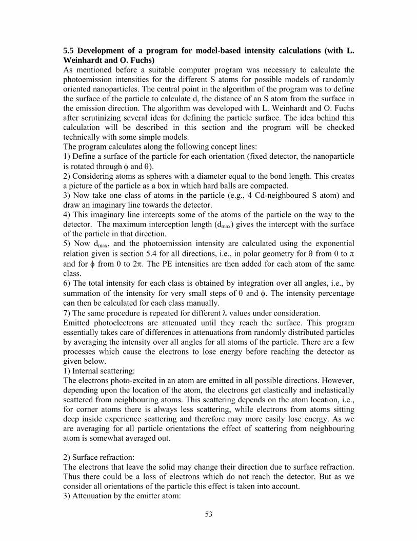
53
5.5 Development of a program for model-based intensity calculations (with L. Weinhardt and O. Fuchs) As mentioned before a suitable computer program was necessary to calculate the photoemission intensities for the different S atoms for possible models of randomly oriented nanoparticles. The central point in the algorithm of the program was to define the surface of the particle to calculate d, the distance of an S atom from the surface in the emission direction. The algorithm was developed with L. Weinhardt and O. Fuchs after scrutinizing several ideas for defining the particle surface. The idea behind this calculation will be described in this section and the program will be checked technically with some simple models. The program calculates along the following concept lines: 1) Define a surface of the particle for each orientation (fixed detector, the nanoparticle is rotated through φ and θ). 2) Considering atoms as spheres with a diameter equal to the bond length. This creates a picture of the particle as a box in which hard balls are compacted. 3) Now take one class of atoms in the particle (e.g., 4 Cd-neighboured S atom) and draw an imaginary line towards the detector. 4) This imaginary line intercepts some of the atoms of the particle on the way to the detector. The maximum interception length (dmax) gives the intercept with the surface of the particle in that direction. 5) Now dmax, and the photoemission intensity are calculated using the exponential relation given is section 5.4 for all directions, i.e., in polar geometry for θ from 0 to π and for φ from 0 to 2π. The PE intensities are then added for each atom of the same class. 6) The total intensity for each class is obtained by integration over all angles, i.e., by summation of the intensity for very small steps of θ and φ. The intensity percentage can then be calculated for each class manually. 7) The same procedure is repeated for different λ values under consideration. Emitted photoelectrons are attenuated until they reach the surface. This program essentially takes care of differences in attenuations from randomly distributed particles by averaging the intensity over all angles for all atoms of the particle. There are a few processes which cause the electrons to lose energy before reaching the detector as given below. 1) Internal scattering: The electrons photo-excited in an atom are emitted in all possible directions. However, depending upon the location of the atom, the electrons get elastically and inelastically scattered from neighbouring atoms. This scattering depends on the atom location, i.e., for corner atoms there is always less scattering, while electrons from atoms sitting deep inside experience scattering and therefore may more easily lose energy. As we are averaging for all particle orientations the effect of scattering from neighbouring atom is somewhat averaged out. 2) Surface refraction: The electrons that leave the solid may change their direction due to surface refraction. Thus there could be a loss of electrons which do not reach the detector. But as we consider all orientations of the particle this effect is taken into account. 3) Attenuation by the emitter atom:
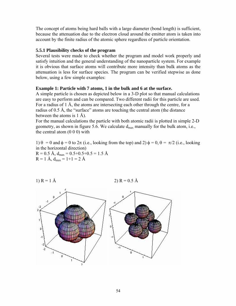
54
The concept of atoms being hard balls with a large diameter (bond length) is sufficient, because the attenuation due to the electron cloud around the emitter atom is taken into account by the finite radius of the atomic sphere regardless of particle orientation. 5.5.1 Plausibility checks of the program Several tests were made to check whether the program and model work properly and satisfy intuition and the general understanding of the nanoparticle system. For example it is obvious that surface atoms will contribute more intensity than bulk atoms as the attenuation is less for surface species. The program can be verified stepwise as done below, using a few simple examples: Example 1: Particle with 7 atoms, 1 in the bulk and 6 at the surface. A simple particle is chosen as depicted below in a 3-D plot so that manual calculations are easy to perform and can be compared. Two different radii for this particle are used. For a radius of 1 Å, the atoms are intersecting each other through the centre, for a radius of 0.5 Å, the “surface” atoms are touching the central atom (the distance between the atoms is 1 Å). For the manual calculations the particle with both atomic radii is plotted in simple 2-D geometry, as shown in figure 5.6. We calculate dmax manually for the bulk atom, i.e., the central atom (0 0 0) with 1) θ = 0 and φ = 0 to 2π (i.e., looking from the top) and 2) φ = 0, θ = π/2 (i.e., looking in the horizontal direction) R = 0.5 Å, dmax = 0.5+0.5+0.5 = 1.5 Å R = 1 Å, dmax = 1+1 = 2 Å 1) R = 1 Å 2) R = 0.5 Å

55
It can be seen from the following plot of dmax versus θ and φ, obtained from the program, that we indeed obtain the values of the manual calculation (marked by dark hallow circles and arrows in the plots) : 1) R = 1 Å 2) R = 0.5 Å
Similarly for the surface atoms the values of manual calculation were obtained with the program. In the following plots, species-resolved photoemission intensity variations for θ and φ is displayed for R = 1 Å and λ = 10 Å
2 A°
Detector
φ = 0, θ = π/2,
θ = 0 and φ = 0 to 2π
(a) Radii = 1 Å (b) Radii = 0.5 Å
1 A°
Figure 5.6: A front view of the particle, for radii 1 Å (a) and 0.5 Å (b). Two detector
positions are shown, i.e., detector at the top and at the side of the particle.
1 A°
Surface atom (1 0 0)
Detector
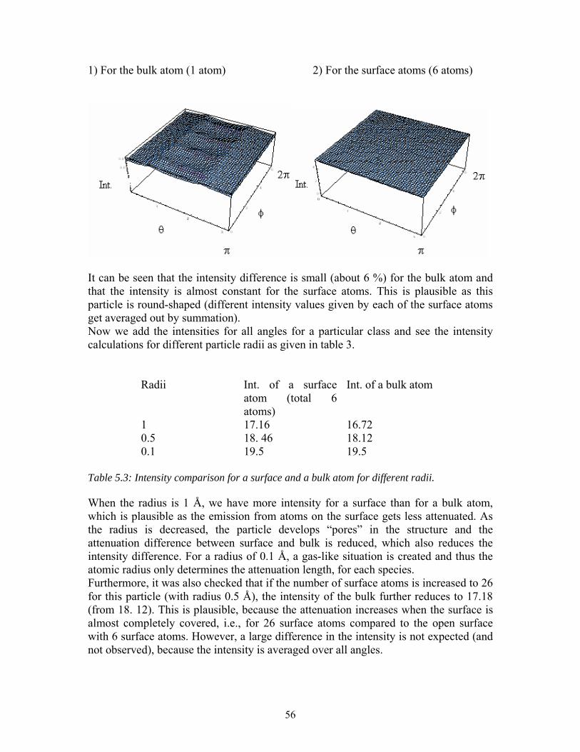
56
1) For the bulk atom (1 atom) 2) For the surface atoms (6 atoms)
It can be seen that the intensity difference is small (about 6 %) for the bulk atom and that the intensity is almost constant for the surface atoms. This is plausible as this particle is round-shaped (different intensity values given by each of the surface atoms get averaged out by summation). Now we add the intensities for all angles for a particular class and see the intensity calculations for different particle radii as given in table 3.
Radii Int. of a surface
atom (total 6 atoms)
Int. of a bulk atom
1 17.16 16.72 0.5 18. 46 18.12 0.1 19.5 19.5
Table 5.3: Intensity comparison for a surface and a bulk atom for different radii. When the radius is 1 Å, we have more intensity for a surface than for a bulk atom, which is plausible as the emission from atoms on the surface gets less attenuated. As the radius is decreased, the particle develops “pores” in the structure and the attenuation difference between surface and bulk is reduced, which also reduces the intensity difference. For a radius of 0.1 Å, a gas-like situation is created and thus the atomic radius only determines the attenuation length, for each species. Furthermore, it was also checked that if the number of surface atoms is increased to 26 for this particle (with radius 0.5 Å), the intensity of the bulk further reduces to 17.18 (from 18. 12). This is plausible, because the attenuation increases when the surface is almost completely covered, i.e., for 26 surface atoms compared to the open surface with 6 surface atoms. However, a large difference in the intensity is not expected (and not observed), because the intensity is averaged over all angles.

57
Example 2: Particle 2 (Structural Model 1 without thiol atoms, i.e., with 26 S and 26 Cd atoms) R = 2.5 Å (bond length of Cd-S)
We plot the species-specific photoemission intensity as a function of θ and φ with λ = 10 Å 1) Intensity for 3-Cd-neighbours
2) Intensity for 4-Cd-neighbors
S atom with 2-Cd -neighbors
S atom with 3-Cd- neighbors
S atom with 4-Cd- neighbors

58
3) Intensity for 2-Cd-neighbors
The results appear sound, because one would expect less variation in the intensities of 3-Cd-neighbored and 4-Cd-neighbored S atoms as a function of θ and φ, as these atoms are located in the model quite symmetrically. Moreover, the intensity of 3-Cd-neighbored, which are situated at the surface of the particle, is higher than that for sulfur atoms with 4-Cd-neighbours. The 2-Cd-neighboured S atoms are situated at the bottom of the particle only and give a maximum intensity when the detector is kept at the bottom, i.e., for θ = π, as seen from the plot. Table 5.4 displays results of the intensity summation over all angles using a numerical integration (and using weight factors, which eliminate extra weight given to axial points in the integration) for different species and for different values of λ. When the value of λ is decreased, the intensity of 4–Cd-neighbors being located in the bulk shows a drop, while the intensities of the 3-Cd and 2-Cd-neighbors which are located at the particle surface show a rise.
Table 5.4: Intensity percentage for each class of S atom for different λ values using the
weighted numerical integration.
5.5.2 Application of the program to the structural models In the following, the program will be applied to model 1, which represents CdS-B, and to model 2, which is a bigger particle and inconsistent with the experimental data of CdS-B (Figure 5.3 (b), section 5.2), applying the “manual” calculation and comparison. Furthermore, in order to see the effect of different λ values in the
Lambda ( Å ) Int. For 4-Cd-N Int. for 2-Cd-N Int. for 3-Cd-N
20 25.76% 24.22% 49.88%
10 24.35% 25.51% 50.13%
7 23.08% 26.69% 50.23%
5 21.35% 28.26% 50.39%

59
calculation, the calculations are done with four different values of λ. Moreover, the program is applied to two more models, which are obtained by modifying the shape of model 1, to check for the effect of the shape of the particle. Calculations for model 3 were not done because it was too far off from the experimental data. 1) Structural Model 1: Total 59 atoms (33 S atoms) Figures 5.7 (a) and (b) show a 3-D plot of model 1 and the results of the program calculations plotted as bar graphs, respectively. It can be seen that the results are similar to those from the manual calculations, i.e., an intensity drop for 4-Cd and 3-Cd-neighboured S atoms and an intensity rise for other species. Thus the program calculation confirms that the model 1 explains the experimental intensity variation of CdS-B. The calculations are done for 4 different values of λ to see the influence of the inelastic mean free path values. As mentioned in section 5.4, two more values were used which were taken from the extreme values of the error margin. If we use the extremal λ values, i.e., λ = 12 Å (720 eV) and 7.5 Å (254 eV), the intensity variations are reduced compared to the average λ values, i.e., λ = 14 Å ± 2 Å V (720 eV) and 5.5 Å ± 2 Å (254 eV). Thus the results are tested for the effect of λ in the calculation and it is safe to say that the model 1 represents CdS-B data for sure. Moreover, to check for the effect of shape variation on the calculations model 1 is modified, as discussed below.
0
5
10
15
20
25
30
35
40
λ = 14 Å (720 eV) λ = 12 Å λ = 7.5 Å λ = 5.5 Å (254 eV)
Frac
tion
of S
2p
Int.
4 Cd-N S-oxide(from 2 Cd-N)
Thiol(attached to 1 Cd-N)
2 Cd-N3 Cd-N
Model1: 33 S atoms
(a) (b)
Figure 5.7: (a) A ball-stick sketch of model 1, (b) bar graph plot for the intensity contributions
and variations of the different S-components as a function of photon energy for model 1. Dark
bars and cross-hatched bars represent photon energies of 720 eV (λ = 14 eV) and 254 eV (λ =
5.5 eV), respectively. In addition, light-gray bars and hatched bars are plotted for λ = 12 eV and
λ = 7.5 eV, respectively. In each case the ordinate shows the fraction of the total S 2p intensity.

60
2) Close to a spherical shape: Structural Model 4 (modification of Model 1, total 60 atoms, 34 S atoms thereof) From the intensity ratios of various S species of model 1, it can be seen that this structural model overestimates the intensity for 3-Cd-neighbored S atoms compared to the experimental data. Therefore, in order to get similar intensity ratios as in the experiment, we modify this model by reducing the number of 3-Cd-neighbored S atoms and introducing more 2-Cd-neighbored atoms (Model 4). Figures 5.8 (a) and (b) show a 3-D plot of Model 4 and the results of the program calculations plotted as bar graph, respectively. It can be seen that this model looks more spherical as compared to model 1 and that the intensity variations are similar to those of model 1. However, the 3-Cd-neighbored S atoms show a very small change in intensity as a function of λ. Moreover, it is interesting to note that the intensity ratio of the different S species now looks very similar to those of the experimental data. Similar to model 1, the fractions of the S 2p intensity are plotted for 4 different values of λ.
3) Away from the spherical shape: Structural Model 5 (modification of Model 1, total 55 atoms, 30 S atoms thereof) Another model which deviates form the spherical geometry is built with 30 S atoms as shown in a 3-D plot in figure 5.9 (a). The intensity calculation results for this model are plotted as bar graphs in figure 5.9 (b). The fraction of S 2p intensity is plotted for
λ = 14 Å (720 eV) λ = 12 Å λ = 7.5 Å λ = 5.5 Å (254 eV)
Model 4: 36 S atoms(modification of Model 1)
4 Cd-N 3 Cd-N Thiol(attached to 1 Cd-N)
2 Cd-N S-oxide(from 2 Cd-N)
Frac
tion
of S
2p
inte
nsity
(a) (b)
Figure 5.8: (a) A 3-D plot of Model 4 from the program, (b) bar graph plot for the intensity
contributions and variations of the different S-components as a function of photon energy.
Dark bars and cross-hatched bars represent photon energies of 720 eV (λ = 14 eV) and 254
eV (λ = 5.5 eV), respectively. In addition, light-gray bars and hatched bars are plotted for λ
= 12 eV and λ = 7.5 eV, respectively. In each case the ordinate shows the fraction of the
total S 2p intensity.

61
different S species for 4 different λ values as done above for model 1 and model 4. This model explains the experimental intensity variation of CdS-B similar to model 1. However, the intensity ratios of the different S species are very different compared to the data, because of very few 4-Cd and 2-Cd-neighbored S atoms in this model (similar to model 1). It can be concluded from the study of different shapes of model 1 (with total 30 – 36 S atoms): 1) The calculations of the intensity variation as a function of photon energy are not much influenced by the particle shape, provided that the basic model is not changed. 2) The intensity ratios of different S components are similar, if the model has an approximately spherical shape. Thus, CdS-B must be a round particle similar to that of the Model 4. 4) Structural Model 2: Total 98 atoms (53 S atoms)
The model is depicted in a 3-D plot in figure 5.10 (a). Figure 10 (b) shows the intensity calculation results for this model plotted as bar graphs. The fraction of S 2p intensity is plotted for different S species for 4 different λ values, similar to model 1. It is interesting to note that the results are similar to those of the manual calculation. This model shows an intensity drop of the 4-Cd-neighbored S atoms only (now the intensity of the 3-Cd-neighbored S atoms shows a rise, in contrast to Model 1) which is not consistent with the experimental intensity variation of CdS-B. Thus it is confirmed here that CdS-B is not a large size particle with 53 S atoms. The value of
0
10
20
30
40
50
60
λ = 14 Å (720 eV) λ = 12 Å λ = 7.5 Å λ = 5.5 Å (254 eV)
Model 5: 30 S atoms(modification of Model 1)
4 Cd-N 3 Cd-N 2 Cd-N S-oxide(from 2 Cd-N)
Thiol(attached to 1 Cd-N)
(a) (b)
Figure 5.9: (a) A 3-D plot of model 5, (b) bar graph plot for the intensity contributions and
variations of the different S-components as a function of photon energy. Dark bars and c
ross-hatched bars represent photon energies of 720 eV (λ = 14 eV) and 254 eV (λ = 5.5
eV), respectively. In addition, light-gray bars and hatched bars are plotted for λ = 12 eV
and λ = 7.5 eV, respectively. In each case the ordinate shows the fraction of the total S 2p
intensity.

62
the XRD size determination (1.7 nm) can be thus reduced to 1.5 + 0.1 nm, since model 2 corresponds to a particle diameter of about 1.7 nm. In order to be more specific, particle sizes from 1.3 to 1.6 nm should be tested with different models, which is in process.
5.6 Summary XPS in combination with variable photon energy excitation appears as a useful technique for the study of very small CdS nanoparticles. The nanoparticles (CdS-A - CdS-D) are associated with five components as constituents of the S 2p signal, the minimum numbers of components for a sufficient representation of the experimental line shapes. Particles with different sizes and capping agents show large differences in the photoemission spectra and also in the beam damage behaviour. With the help of previous knowledge of photoemission of CdS nanoparticles, the assignment of the components is done for CdS-A and CdS-B based on the intensity variation of these components as a function of photon energy and beam damage. The main constituents of the signal are S atoms with different numbers of Cd neighbors, S atoms from thiol,
0
10
20
30
40
50
λ = 14 Å (720 eV) λ = 12 Å λ = 7.5 Å λ = 5.5 Å (254 eV)
Model 2: 53 S atoms
S-oxide(from 2 Cd-N)
Thiol(attached to 1 Cd-N)
2 Cd-N3 Cd-N4 Cd-N
Frac
tion
of S
2p
Int.
(a) (b)
Figure 5.10: (a) Ball-stick sketch of model 2, (b) bar graph plot for the intensity contributions and
variations of the different S-components as a function of photon energy. Dark bars and cross-
hatched bars represent photon energies of 720 eV (λ = 14 eV) and 254 eV (λ = 5.5 eV),
respectively. In addition, light-gray bars and hatched bars are plotted for λ = 12 eV and λ = 7.5
eV, respectively. In each case the ordinate shows the fraction of the total S 2p intensity.
63
and S atoms in a partially oxidized state. The assignment of CdS-B cannot be applied to CdS-A, which indicates that each particle needs a separate consideration. Focusing on CdS-B, a new approach is followed in order to understand the differences and minor details of the spectra. This is done by a structural model-based photoemission intensity calculation and comparative study for CdS-B. The results show that out of 3 different models chosen for CdS-B, model 1 can explain the intensity variations of the data. Moreover, the failure to explain the data with a bigger particle hints towards photoemission as a tool for size determination of very small particles. To check the various parameters involved, a computer program for the calculations was used. The required mean free paths for our experimental photon energies were estimated using the TPP-2 and CS 2 equations given by Seah et al. and Powell et. al. The application of this program to models 1 and 2 confirms the results of the manual calculation. Moreover, it is found that the λ value used in the calculations does not produce significant differences in the intensity variations of different S species. In order to see the effect of particle shape, model 1 was modified to a more spherical shape (model 4) and a less spherical shape (model 5). It is interesting that model 4 not only explains the intensity variations but also shows a close match to the intensity ratios of the various S species of the experimental data of CdS-B. The two important messages of this study are that the CdS-B is a particle with a size below 1.7 nm (53 S atoms, model 2, big size particle) and probably has a spherical shape. Thus this new analysis of photoemission spectra offers a way to estimate the particle size and to some extent the particle shape, in the present case. However, there is a need to extend this study beyond the four models treated in this thesis. In this view, the calculations for model 3 and several more models using this program are in progress.

64

65
Chapter 6 Band gap opening in CdS nanopatricles (NEXAFS+ VBPES)
The high-resolution photoemission study of CdS nanoparticles of the preceding chapter revealed that the particles with different sizes show very different spectra. In this chapter combined experiments of valence band photoemission (VBPES) and near edge x-ray absorption (NEXAFS) are presented in order to study the band gap opening in CdS nanoparticles. The characteristic absorption edges, which can be measured in NEXAFS, correspond to the onset of the transition of electrons from core states to unoccupied states above
the Fermi level. NEXAFS has been applied to the nanoparticles only in last few years [84-87] although this is a potential technique for understanding the conduction bands of the nanoparticles.
Figure 6.1: Left: Valence band photoemission (VBPES) of four differently sized nanoparticles at
a photon energy of 200 eV. Right: S L2, 3 X-ray absorption spectra. Linearly extrapolated grey
lines show the valence band edge and the absorption edge. Grey arrows gives the distance
between the two edges and hence indicate the band gap opening. The sizes of the particles are
given above the grey arrows.

66
A band gap opening in CdS nanoparticles was previously reported by Lüning et al. [85], using a combination of NEXAFS and X-ray emission spectroscopy. They found that the band gap opening has about equal contributions from the valence and conduction band shift, in good agreement with an effective mass approximation with finite potential walls. The first shoulder in NEXAFS (at a photon energy of 162.7 eV) was assigned to a Wannier-type core exciton. With decreasing size, the energy separation between the exciton and the conduction-band related absorption features increased. Thus, the apparent absorption onset is size independent, while there is a shift of the unoccupied states to higher energies. In contrast to these data [85], Nowak et al. [86] observe a drop in intensity of this core exciton with decreasing particle size, which is interpreted as a Frenkel-type exciton. In contrast, for a Wannier-type exciton, the oscillator strength increases with decreasing particle size. Previously, NEXAFS was applied in our group by Uli Winkler [84] to characterize MPA-capped CdS nanoparticles. The results show similarities with the work of Lüning et al. [85]. In the present study, TG-capped CdS nanoparticles are characterized by using NEXAFS in combination with VBPES. The NEXAFS and VBPES
S 2p Bulk
1 eV
163 eV 162.7 eV 162.5 eV
2.7 eV3.8 eV4.3 eV
1.5 eVEf
CBM
VBM
1.2 eV
161.5 eV
2.3 nm1.8 nm1.1 nm
∆Eoptical
CdS-NP
4.3 eV 3.5 eV 3.3 eV
162.9 eV
4.2 eV
1.4 eV
1.4 nm
3.9 eV
Figure 6.2. Schematic energy level diagram of 2.3 nm, 1.4 nm,1.8 nm, and 1.1 nm CdS
nanoparticles. The distance (∆E ± 0.1 eV) of the valence band maximum (VBM) and the
absorption onset ("conduction band minimum", CBM) with respect to the Fermi energy (Ef)
are shown. The optical band gap(∆Eoptical) is given at the top of the diagram.
67
measurements show spectral differences as a function of sample position, similar to the high-resolution photoemission observations which are due to the drop deposition method (see Chapter 7). Therefore the spectra were collected for a large number of sample positions, and as fast as possible to account for spot variation and to minimize radiation damage. Figure 6.1 displays a set of data showing the band gap opening in TG-capped CdS nanoparticles. The spectra were calibrated using an Au reference sample. S 2p photoemission experiments do not exhibit any binding energy shift of the component with lowest binding energy (component I), i.e., bulk, as a function of size. In contrast, we find a shift of the valence band edge (as shown by grey lines linearly extrapolated to the dotted base line) to higher binding energies with decreasing particle size, in agreement with the work of Colvin et al. [87]. The broad feature from about 5 eV to 9 eV is the valence band of the particles. In comparison to the bulk CdS valence band (obtained by angle resolved photoemission) the valence band of nanoparticles is not very much structured due to the random orientations of the crystal structure of the particles thus smearing out dispersion effects if these exist in such small particles [87]. A small shoulder observed before the valence band of the nanoparticles (which is not equal for all particles) arises due to impurity or defect levels in the band gap of these particles. A prominent feature at about 12 eV belongs to the Cd 4d level. The right part of Fig. 6.1 shows the x-ray absorption spectra of the nanoparticles at the S L2 3 edge. The results are similar to those published in [85], i.e., they show a shift of the absorption edge (as shown by grey lines) with decreasing size and a size-independent core exciton peak at 162.5 eV (dotted vertical line). In contrast to [85], the intensity of this peak decreases as a function of particle size, in agreement with the results of Nowak et al. [86]. There is a possibility that this excitonic peak arises due to a resonance of the capping molecule. However, the x-ray absorption spectra for thioglycerin at the S L2 3 do not show an absorption at this position (162.7 eV) [86] which rules out this interpretation. Figure 6.2 gives a schematic diagram of the electronic band structure of TG-capped CdS nanoparticles, plotted using the energy separation (error bar: ± 0.1 eV) of the valence band maximum (VBM) with respect to the Fermi energy and the absorption edge with respect to the S 2p core level binding energy (161. 5 ± 0.1 eV). This implicitly assumes that the S 2p hole is fully screened, or in other words, that the S 2p binding energy equals the S 2p position in the ground state. Values for the optical band gap, as derived from the UV-VIS spectroscopy, are given for comparison. For the larger particles the measured gap is comparable to the optical gap, while for the smallest particles (1.1 nm), the measured gap is larger by about 1.5 eV. This difference is attributed to the enhanced electron-hole correlation for optical absorption in small particles and to the difference between exciton and band edge in our NEXAFS data. Further detailed investigations of edge positions and final state effects are underway to interpret the results in a detailed quantitative picture.

68

69
Chapter 7 Additional investigations on CdS nanopaticles
In this chapter we will address some additional investigations on CdS nanoparticles to learn more about the effects of beam exposure, annealing, film preparation, etc. The first section (7.1) of this Chapter deals with laboratory XPS experiments carried out on the particles to learn about the quality of a nanoparticle film. As it will be shown, in order to achieve good signal to noise ratios the nanoparticle film should be prepared from a freshly synthesized nanoparticle solution. This also reduces charging effects. Important information about the surface termination of these particles can already be obtained from the relative intensities of S and Cd peaks. Results of annealing experiments on the TG-capped nanoparticles particles are presented in the next section (7.2). In section 7.3 beam damage results for CdS-B are discussed to stress that the different components of photoemission spectra are not a manifestation of beam damage. The next section (7.4) focuses on spectral variations due to the influence of the thin film preparation techniques used for the nanoparticles. Micro-Raman experiments on these nanoparticles will be presented at the end of this chapter (7.5), where we compare TG and the TG-capped nanoparticles to learn more about the capping. 7.1 Laboratory XPS investigations of nanoparticle films As mentioned before a uniform thin film is required in order to obtain a good signal in the photoemission experiments and to reduce the influence from the substrate. This is achieved either by drop deposition or by electrophoretic deposition from the nanoparticle solution. The thin films prepared in this way were initially tested with XPS using an x-ray tube to see various constituents of the nanoparticle, signal quality of the nanoparticle film, etc. Figure 7.1 shows overview XPS spectra for CdS-B. The lower spectrum is recorded on a thin film sample prepared from a fresh nanoparticle solution while the upper spectrum is recorded on a thin film sample prepared from nanoparticle powder redispersed in water. The inset shows detailed scans of the Cd 3d and S 2p levels. An excitation energy of 1253.6 eV was employed using the MgKα source. The prominent peaks are marked by thick vertical lines and labelled. The spectra are normalized to equal Cd 3d intensity The large increase in the Au 4f peaks for the film prepared from nanoparticle powder as compared to the film prepared from fresh solution is because of the higher contribution from the substrate indicating that the particles may not be deposited uniformly. Furthermore, in order to check for charging, Cd 3d and S 2p spectra were compared with and without shining a halogen lamp on the films. The spectra show no differences for fresh solution films while there is a shift towards lower binding energy of about 150 meV for the powder prepared films when the halogen lamp is switched on. This indicates charging of the powder prepared film. Thus it can be said that the films prepared by redispersing nanoparticle powder produces lumps of particles on the substrate with lots of open substrate sites while the films prepared from fresh solutions are more uniform and give a higher signal from the particles because these are well distributed over the substrate. Other samples were also

70
checked for charging and signal quality with similar results. In order to find out the termination of the particles, the intensities of S 2p and Cd 3d peaks were compared. The photoemission intensity is a function of analyzer transmission function (T), electron inelastic mean free path (λ), and photoionisation cross section (σ), which are functions of the kinetic energy. It has been checked for our MK 2 analyser that the transmission function varies as 1/ E 0.5 in the kinetic energy range of interest (for S and Cd). It is very difficult to know the mean free path for the kinetic energies as the film thickness is not known, the films are not homogeneous, and the capping molecules also attenuate the signal of Cd and S differently. Therefore the mean free path can be slightly different for different positions on the sample which in fact averages out in XPS. Hence we consider the mean free path variation versus kinetic energy from the universal curve as E 0.5 [21]. For simplicity, the transmission and mean free path dependence are cancelled out, and the intensity is now a function of the cross sections only. So it is appropriate to divide the Cd and S intensities by the corresponding cross sections. In this way the obtained normalised intensity of S and
1000 800 600 400 200 0
{
{
{Cd MNN
Cd 3d
C 1S
C Auger
O Auger Au 3d
O 1S
S 2p
Au 4f
Binding Energy (eV)
CdS-B (d ~ 1.4 nm)
XPSMg Kα1253.6 eV
Inte
nsity
powder dissolved in waterfreshly synthesized solution
418 416 414 412 410 408
Cd 3d3/2
Binding Energy (eV)170 168 166 164 162 160
Binding Energy (eV)
S 2p
Figure 7.1: Overview laboratory XPS spectra of CdS-B (d ~ 1.4 nm) for a film prepared from
a freshly synthesized nanoparticle solution (black) and for a film prepared from a dried
nanoparticle powder dissolved in water (gray). The spectra are normalized to the Cd 3d
intensity in order to highlight the difference in the Au 4f intensity for the two films. The inset
shows Cd 3d3/2 and S 2p spectra from the film prepared from the fresh nanoparticle solution
normalized to equal height. The spectra were recorded with a photon energy of 1253.6 eV
(Mg Kα).
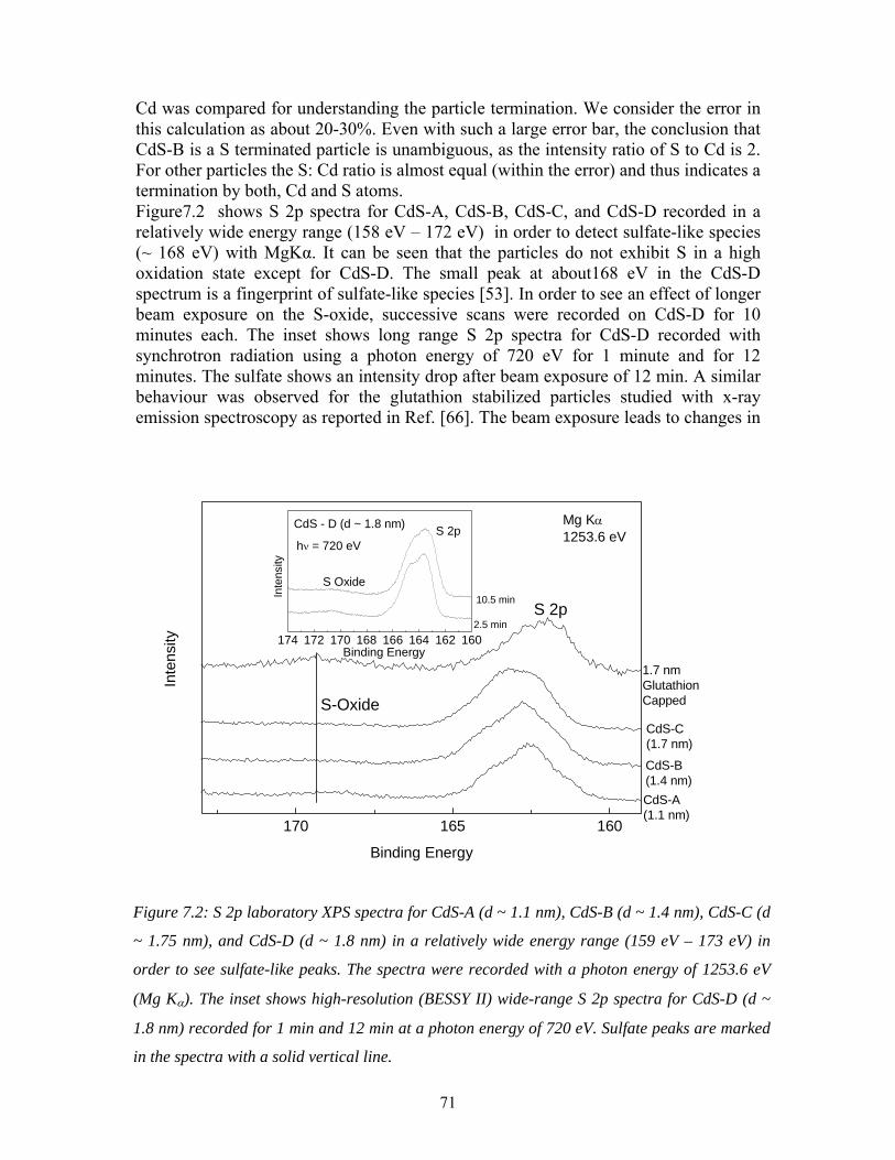
71
Cd was compared for understanding the particle termination. We consider the error in this calculation as about 20-30%. Even with such a large error bar, the conclusion that CdS-B is a S terminated particle is unambiguous, as the intensity ratio of S to Cd is 2. For other particles the S: Cd ratio is almost equal (within the error) and thus indicates a termination by both, Cd and S atoms. Figure7.2 shows S 2p spectra for CdS-A, CdS-B, CdS-C, and CdS-D recorded in a relatively wide energy range (158 eV – 172 eV) in order to detect sulfate-like species (~ 168 eV) with MgKα. It can be seen that the particles do not exhibit S in a high oxidation state except for CdS-D. The small peak at about168 eV in the CdS-D spectrum is a fingerprint of sulfate-like species [53]. In order to see an effect of longer beam exposure on the S-oxide, successive scans were recorded on CdS-D for 10 minutes each. The inset shows long range S 2p spectra for CdS-D recorded with synchrotron radiation using a photon energy of 720 eV for 1 minute and for 12 minutes. The sulfate shows an intensity drop after beam exposure of 12 min. A similar behaviour was observed for the glutathion stabilized particles studied with x-ray emission spectroscopy as reported in Ref. [66]. The beam exposure leads to changes in
170 165 160
174 172 170 168 166 164 162 160
Inte
nsity
Mg Kα1253.6 eV
S 2p
S-Oxide
CdS-B (1.4 nm)
CdS-C (1.7 nm)
1.7 nmGlutathion Capped
CdS-A (1.1 nm)
Inte
nsity
Binding Energy
CdS - D (d ~ 1.8 nm)
S Oxide
S 2p
10.5 min
2.5 min
hν = 720 eV
Binding Energy
Figure 7.2: S 2p laboratory XPS spectra for CdS-A (d ~ 1.1 nm), CdS-B (d ~ 1.4 nm), CdS-C (d
~ 1.75 nm), and CdS-D (d ~ 1.8 nm) in a relatively wide energy range (159 eV – 173 eV) in
order to see sulfate-like peaks. The spectra were recorded with a photon energy of 1253.6 eV
(Mg Kα). The inset shows high-resolution (BESSY II) wide-range S 2p spectra for CdS-D (d ~
1.8 nm) recorded for 1 min and 12 min at a photon energy of 720 eV. Sulfate peaks are marked
in the spectra with a solid vertical line.

72
the S 2p spectra (162 -166 eV) apart from the oxide dissociation, which is the subject of a detailed analysis as presented in section 7.3. 7.2 Thermal stability of CdS nanoparticles The thermal behavior of CdS nanoparticles with MPA capping was investigated earlier in our group by Winkler et al. [88]. It was observed that the nanoparticle surface, which is S-terminated at room temperature, changes after annealing by removal of capping S atoms, agglomeration, and segregation of Cd atoms. The result of this process depends on the particle size and is much more pronounced for large particles. Annealing temperatures of 190 °C and 240 °C were used in this study. As described in Chapter 4, the size distribution can be narrowed, and smaller sizes can
be synthesized using TG rather than MPA capping. The thermal stability of our TG-capped nanoparticles was examined by annealing the particles for different temperatures and measuring XPS spectra in the laboratory. Figure 7.3 shows S 2p (a) and Cd 3d scans (b) for CdS nanoparticles (d ~ 2.4 nm) recorded at a photon energy of 1253.6 eV (MgKα). The figure shows spectra recorded at room temperature and after 10 min of annealing at temperatures of 130 to 210 ° C. Note that, larger particles (2.4 nm, diameter evaluated by optical absorption and TBM) are used for this study, and a thin film of these particles was produced by drop deposition from freshly synthesized solution. In addition, the samples are illuminated by a halogen lamp during the measurements in order to minimize charging effects. The S 2p and Cd 3d spectra show
177 174 171 168 165 162 159
160 °C
190 °C
130 °C
30 °C (RT)
210 °C
hν = 1256. 3eVannealing for 10 min
SOX
CdS-NP, 2.4 nm
(a) S 2p
inte
nsity
(a.u
.)
Binding Energy (eV)
415 410 405 400
hν = 1256. 3eVannealing for 10 min
210 °C
160 °C
190 °C
130 °C
30 °C (RT)
CdS-NP, 2.4 nm
(b) Cd 3d
inte
nsity
(a.u
.)
Binding Energy (eV)
Figure 7.3: S 2p (a) and Cd 3d (b) XPS spectra for CdS nanoparticles (d ~ 2.4 nm) at room
temperature (30 °C) and after annealing (10 minutes) for different temperatures from 130 °C
to 210 °C. The spectra were recorded with a photon energy of 1253.6 eV (Mg Kα).

73
significant changes in the line widths and positions after annealing. However, the changes in Cd 3d spectra can be seen more clearly since the spectra are less noisy than the S 2p spectra. It can be seen that, during annealing above 130 °C, the intensity at higher binding energy is reduced. This indicates the reduction of surface near S-species, which may be due to dissociation of TG from the particle surface. Furthermore, S-oxide starts showing up indicating oxidation of the particles because of the loss of the capping molecules. At 210 °C the spectra show a shift of about 0.4 eV towards lower binding energy which resembles the position of bulk CdS. The Cd 3d spectra were fitted with 2 peaks using Gaussian line shapes (not shown here because of the poor resolution of XPS spectra recorded in the laboratory using x-ray tube), which confirms these spectral changes and supports the interpretation. The results of the annealing experiments on the TG are similar to those of MPA-capping reported by Winkler et al. previously [88], however the changes occur for TG at smaller temperatures which indicates that the TG-capped particles posses less thermal stability. From this study trends can be derived, but in order to understand the details of the intensity changes high-resolution measurements have to be performed. The problem in the high-resolution annealing experiments is the spectral changes due to the beam damage (as mentioned in the Chapter 5) in addition to the annealing, which may lead to difficulties in the data interpretation. However, fast scans recorded within a minute can eliminate the damage problem as discussed in the next section.
7.3 Effects of a beam damage In this section a systematic study of beam damage effects is presented. Exposure to a soft X-ray beam induces changes in the organic material and organically capped nanoparticles, as studied earlier for S 2p photoemission lines in alkanethiols [89, 90], copper chelate [91], and recently in CdS nanoparticles by Eychmüller et al. [69]. Photoelectron spectroscopy offers a unique way of investigating surfaces of nanoparticles, and this needs a good understanding of beam-induced spectral variations with time. To study beam damage, S 2p photoemission spectra for CdS-A, CdS-B, and CdS-D were collected successively for 12 minutes with a beam exposure of about 1 minute per scan. Figure 7.4 (a) consists of 3 spectra taken with beam exposure times of 1 min, 6 min and 11 min for CdS-B. The three spectra were analysed by careful peak fits in order to quantify intensity changes as a function of beam exposure time. The intensity changes of the different components (see chapter 5 for more details about the fits) are evident from figure 7.4 (a). However, it is useful to follow the trends in more detail and to extrapolate to time zero. Therefore the intensities of the components (peak areas) are plotted as a function of beam exposure time in figure 7.4 (b), with error bars to take into account possible variations of the data points. Figure 7.4 (c) and (d) show two spectra with fits each for CdS-A and CdS-D recorded after beam exposures of 1 min and 12 min, respectively. It can be seen that for all particles, beam damage produces a rise of spectral features at lower binding energy, related to an enhancement of the bulk contribution. The TG-capped particles (CdS-A, and CdS-B) are more sensitive to beam damage than the glutathion-capped particles (CdS-D). Furthermore, TG-capped particles of different sizes show differences in their

74
beam damage behavior. The smaller particle (CdS-A) shows a larger variation in the sulfur components with beam exposure compared to CdS-B. The intensity changes of the components of CdS-A and CdS-B are already discussed
Figure 7.4: X-ray photoemission S 2p core level spectra for (a) CdS-B (d ~ 1.4 nm), (c) CdS-
A (d ~ 1.1 nm), and (d) CdS-D (d ~ 1.8 nm). For CdS-A and CdS-D, the spectra were
recorded with beam exposure times of 1 min and 11 min each. For CdS-B, the spectra were
recorded with three different beam exposure times, (1) 1 min, (2) 6 min, and (3) 12 min. The
experimental data are shown as solid squares, the solid lines represent fits. For CdS-B (d ~
1.4 nm), the S 2p intensities for the different S-components (I-V) are shown as a function of
beam exposure time (b). The data for component I are extrapolated to zero as shown by the
line joining solid triangles.

75
in section 5 together with the component assignment. CdS-D looks overall stable under the beam; however there are small changes of the sulfur components. Component III increases while component V decreases. Component V was assigned as S atom in a partially oxidized state for TG-capped nanoparticles (section 5.1). Similarly for CdS-D, component V may belong to a partially oxidized S atom. The drop of this component as a function of beam exposure is consistent with the drop of the sulfate species (BE: 168 eV) as discussed in section 7.1 (figure 7.2). We now focus on spectral changes of CdS-B, as structural information is available for this particle. It can be seen that, except for components IV and I, the changes of the other components are within the error bars. Hence they may be considered to be constant. Component I shows an intensity rise with increasing beam exposure time. It is extrapolated to zero time (see the line joining the solid triangles) to indicates its existence at time zero. This proves that component I is neither an artifact nor a product of beam-damage but that it does stem from the pristine nanoparticles. The studies on CdS nanoparticles by Eychmüller et al. [54], however, suggest that the
different components of the S 2p spectrum are a consequence of beam damage. This is based on a comparison of the XPS signals of a Cd-thiolate compound with those of nanoparticles and on X-ray absorption studies. In contrast, we find that thiol-capped nanoparticles resist to beam exposure for a relatively long time. However, we find hat the damage of Cd-thiolate occurs on a very fast time scale compared to that of the nanoparticles. This can be proved by laboratory XPS measurements on Cd-thiolate, which show severe changes in the S 2p spectra with X-ray exposure (figure 7.5) for a wet chemically synthesized Cd- thiolate compound. Three doublets (using Voigt line shapes) are fitted to the 9- and 20- minutes-spectra, while 4 Voigt doublets are required for the 114-min-spectra. The fits highlight the changes in the line shapes as a function of beam exposure. Compared to synchrotron radiation, the X-ray flux of the laboratory source is by at least 4 orders of magnitude smaller, and the spot area is about 100 - 1000 times larger. This
Figure 7.5: Laboratory XPS spectra of S 2p core
levels for cadmiumthiolate recorded at 1253.6 eV
(Mg Kα) after 9 min, 20 min, and 114 min of X-ray
exposure. The different S 2p Voigt doublet fits (solid
lines, 9 and 20 min: 3 doublets; 114 minutes:4
doublets) highlight the beam-induced changes in the
spectra.

76
results in a 106 – 108 times smaller flux density on the sample compared to synchrotron radiation. The changes in cadmium thiolate induced by X-rays within a time scale of 9 min to about 2 hrs (the time needed for reasonably good spectra as shown in fig. 7.5) can be estimated to occur more than 100 times faster in the synchrotron beam as compared to a laboratory source. Thus the data on Cd-thiolate of ref. [54] are indeed due to beam damage while those taken with a laboratory source (bottom spectra of fig. 7.5) are much less affected.
Our nanoparticle spectra do not change on the time scale of those of cadmium thiolate. However, the photoemission spectra recorded with SR on a thin film nanoparticle sample with a beam exposure of about 1 min are still representative for (rarely) unaffected nanoparticles. Thus, the various sulfur components observed are indeed representative for the different sulfur sites in the pristine particles (as discussed in section 5.1). Moreover, the intensity changes of these components with beam exposure provide important additional information for the assignment of the sulfur components. We emphasize that the beam damage mechanism is different for the different particles. 7.4 Influences of thin film preparation methods Most of the thin film samples for the photoemission measurements were prepared by drop deposition. However, for some samples also the electrophoresis technique was used. In the following, changes in the S 2p photoemission spectra due to the film deposition technique are discussed.
Figure 7.6: X-ray photoemission S 2p core level spectra of CdS-B for two different spots on
the rim of the drop-dried nanoparticle sample at photon energies of 720 eV and 254 eV.
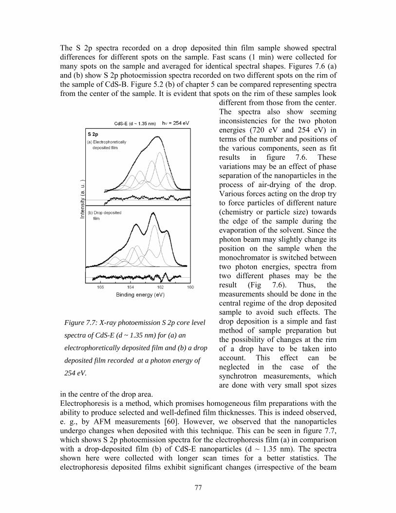
77
The S 2p spectra recorded on a drop deposited thin film sample showed spectral differences for different spots on the sample. Fast scans (1 min) were collected for many spots on the sample and averaged for identical spectral shapes. Figures 7.6 (a) and (b) show S 2p photoemission spectra recorded on two different spots on the rim of the sample of CdS-B. Figure 5.2 (b) of chapter 5 can be compared representing spectra from the center of the sample. It is evident that spots on the rim of these samples look
different from those from the center. The spectra also show seeming inconsistencies for the two photon energies (720 eV and 254 eV) in terms of the number and positions of the various components, seen as fit results in figure 7.6. These variations may be an effect of phase separation of the nanoparticles in the process of air-drying of the drop. Various forces acting on the drop try to force particles of different nature (chemistry or particle size) towards the edge of the sample during the evaporation of the solvent. Since the photon beam may slightly change its position on the sample when the monochromator is switched between two photon energies, spectra from two different phases may be the result (Fig 7.6). Thus, the measurements should be done in the central regime of the drop deposited sample to avoid such effects. The drop deposition is a simple and fast method of sample preparation but the possibility of changes at the rim of a drop have to be taken into account. This effect can be neglected in the case of the synchrotron measurements, which are done with very small spot sizes
in the centre of the drop area. Electrophoresis is a method, which promises homogeneous film preparations with the ability to produce selected and well-defined film thicknesses. This is indeed observed, e. g., by AFM measurements [60]. However, we observed that the nanoparticles undergo changes when deposited with this technique. This can be seen in figure 7.7, which shows S 2p photoemission spectra for the electrophoresis film (a) in comparison with a drop-deposited film (b) of CdS-E nanoparticles (d ~ 1.35 nm). The spectra shown here were collected with longer scan times for a better statistics. The electrophoresis deposited films exhibit significant changes (irrespective of the beam
Figure 7.7: X-ray photoemission S 2p core level
spectra of CdS-E (d ~ 1.35 nm) for (a) an
electrophoretically deposited film and (b) a drop
deposited film recorded at a photon energy of
254 eV.

78
damage) that lead to a bulk CdS like spectrum, which is a strong indication for agglomeration. The agglomeration may be due to a breaking of thiols during the deposition process. 7.5 Raman: Comparison of TG and CdS nanoparticles (with C. Dem and M.
Schmitt) Among the various techniques for a “bulk characterization” of nanoparticles, Raman spectroscopy is used in a few cases only [66, 92-95]. Small intensities of the Cd-S stretching frequencies (e.g., reported by Lover et al. [92]) inhibit the use of this technique in many cases. The thioglycerol (TG)-capped CdS nanoparticles were investigated with Raman in order to identify different vibrational modes of the particles. To learn more about the Cd-S bonds, low frequency Raman studies havebeen
performed with an UV excitation source allowing resonant-Raman spectroscopy. Recently, such resonant Raman measurements have been done for two nanoparticle sizes. The interpretation of the data is in progress. In the following, micro-Raman measurements are presented to highlight the differences between the TG molecules and the TG-capped nanoparticles to study the vibrational behaviour in the capping
500 1000 1500 2000 2500 3000
2571
2921
222 Micro Raman
632 nm Laser
1.7 nm2.1 nm
1.4 nmThioglycerol
Wavenumber (cm-1)
Ram
an in
tens
ity
Figure 7.8: Micro-Raman spectra recorded with 632 nm laser excitation for thioglycerol
(TG) molecules in solution and for TG-capped CdS nanopaticles of three different sizes.
(d ~ 1.4 nm, 1.7 nm, and 2.1 nm).

79
molecule. Furthermore, it is attempted to identify the different vibrational modes of TG with the help of previous reports and theoretical calculations. Figure 7.8 shows micro-Raman spectra for TG and TG-capped CdS nanoparticles of three different sizes. The CdS-nanoparticles exhibit a large peak at about 222 cm-1, which is a fingerprint of Cd-S bonds, and several other peaks at higher wave numbers, which are due to the capping thioglycerol. TG in solution shows a large peak at 2571 cm-1 representing the S-H bond. A large peak also appears in all spectra at 2921 cm-1, which represents CH2 bonds [91] The major difference between TG in solution and TG-capped nanoparticles is the complete disappearance of the S-H frequency for the nanoparticles. Thus we can say that all of the capping is washed out or utilized for the formation of thiol bonds at the particles surface. Furthermore, there are some differences in the TG and nanoparticle spectra in the frequency regime of 500 to 1200 cm-1 as shown in figure 7.9. The vibrational frequencies at 773 cm-1 and 930 cm-1 of TG are absent in the particles. They may belong to different modes of the S-H vibration (see table 7.1). In order to compare and differentiate between TG and particle vibrations, an identification of all frequencies of TG appears necessary. A theoretical calculation of thioglycerol vibrational frequencies was performed by Vitalyi Shklover of our group using the Gaussian 98 program (using a DFT based approch). Furthermore, the calculation was also done by replacing H from thiol with a Cd atom in order to see the changes in the frequencies of TG after it binds with the nanoparticles. The results of the calculation are compared with the experimental frequencies in table 7.1. It can be seen that the calculation agrees quite nicely with the data. However, some of the vibrational frequencies of the data do not appear in the calculation. Moreover, the calculation shows some additional vibrations which are not present in the data. The calculation also shows the presence of a vibrational mode at 940 cm-1 similar to the
600 800 1000 1200
Micro Raman632 nm Laser
930
778
1.7 nm
2.1 nm
1.4 nm
Thioglycerol
Wavenumber (cm-1)
Ram
an in
tens
ity
Figure 7.9: Enlarged view of the micro-Raman spectra of figure 7.8 showing differences
in the vibrational modes of thioglycerol (TG) and for TG-capped CdS nanopaticles
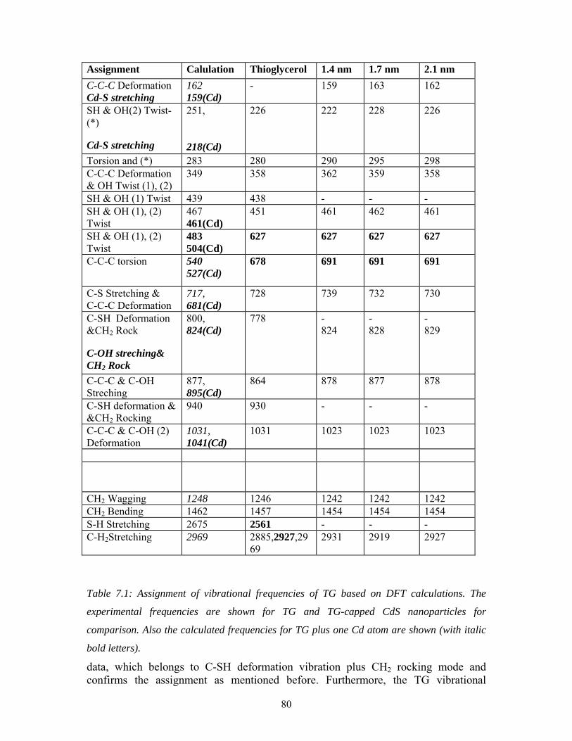
80
Table 7.1: Assignment of vibrational frequencies of TG based on DFT calculations. The
experimental frequencies are shown for TG and TG-capped CdS nanoparticles for
comparison. Also the calculated frequencies for TG plus one Cd atom are shown (with italic
bold letters).
data, which belongs to C-SH deformation vibration plus CH2 rocking mode and confirms the assignment as mentioned before. Furthermore, the TG vibrational
Assignment Calulation Thioglycerol 1.4 nm 1.7 nm 2.1 nm C-C-C Deformation Cd-S stretching
162 159(Cd)
- 159 163 162
SH & OH(2) Twist- (*)
Cd-S stretching
251, 218(Cd)
226 222 228 226
Torsion and (*) 283 280 290 295 298 C-C-C Deformation & OH Twist (1), (2)
349 358 362 359 358
SH & OH (1) Twist 439 438 - - - SH & OH (1), (2) Twist
467 461(Cd)
451 461 462 461
SH & OH (1), (2) Twist
483 504(Cd)
627 627 627 627
C-C-C torsion 540 527(Cd)
678 691 691 691
C-S Stretching & C-C-C Deformation
717, 681(Cd)
728 739 732 730
C-SH Deformation &CH2 Rock
C-OH streching& CH2 Rock
800, 824(Cd)
778 - 824
- 828
- 829
C-C-C & C-OH Streching
877, 895(Cd)
864 878 877 878
C-SH deformation & &CH2 Rocking
940 930 - - -
C-C-C & C-OH (2) Deformation
1031, 1041(Cd)
1031 1023 1023 1023
CH2 Wagging 1248 1246 1242 1242 1242 CH2 Bending 1462 1457 1454 1454 1454 S-H Stretching 2675 2561 - - - C-H2Stretching 2969 2885,2927,29
69 2931 2919 2927

81
frequency at 778 cm-1 is formed at 824 cm-1 in the calculation done on TG plus one Cd atom. It is to be noted that the calculation exhibits shifts of the vibrational modes of TG when a Cd atom is added, thus coming close to the experimental data. There are some frequencies in the data which are not identified by this calculation. May be the calculations have to be improved and checked with more Cd atoms attached to TG, which is in process. 7.6. Summary In summary, the XPS measurements performed in the laboratory reveal important aspects such as the nanoparticle film quality, the oxidation, and the surface termination. The films produced from a freshly synthesized nanoparticle solution are fairly homogeneous and non-charging. The annealing of TG-capped CdS nanoparticles results in spectra that indicate dissociation of TG from the particle surface, similar to the earlier results of MPA-capped nanoparticles. The beam-induced effects play a major role; however, the knowledge of the time scale for such effects gives the possibility to record photoemission spectra with fairly good signal quality and to extrapolate the changes to zero radiation exposure, i. e., to the undamaged samples. Cadmiumthiolate has a very short time scale for beam damages compared to the nanoparticles. Thus the components of the S 2p spectra measured on nanoparticles are not a result of beam damage but reliable representation of the initial state. Particles with different sizes and capping show different beam damage behaviour. The thin film preparation by electrophoresis shows significant changes in the spectrumindicating agglomeration, while the drop deposition technique points towards spectral changes on the rim of the dried drop, which can be neglected by focusing the excitation beam on the center. The micro-Raman measurements highlight major differences in the spectra of TG in solution and TG-capped nanoparticles, e. g. the complete absence of the S-H vibrations for the nanoparticles, thus indicating consumption or removal of all TG molecules after reaction. Furthermore, there are additional differences in the vibrational modes, which are partly identified by the calculations performed by V. Shklover.

82

83
Chapter 8 Summary and Outlook
Very small, thioglycerol (TG)-capped CdS nanoparticles were synthesized by a wet chemical technique and investigated in the framework of this thesis. Also glutathione-capped particles were investigated for a comparison of the capping agents. High-resolution photoelectron spectroscopy using high-brilliance synchrotron radiation was applied as the major tool for the characterization of these particles. Additionally, the particles were investigated with UV-VIS absorption spectroscopy, XPS using a laboratory source, valence band photoemission spectroscopy (VBPES), near-edge x-ray absorption spectroscopy (NEXAFS), and micro-Raman spectroscopy to address various aspects of the particles. In the beginning, an overview on size quantization effects is given to create a theoretical background behind the work presented in this thesis. Furthermore, an overview of various conventional techniques for size determination is presented. Exact information about size, shape and size distribution of nanoparticles is not yet achievable because of experimental limitations of the various size determination methods. Nanoparticles, with a range of sizes from 1.1 to 4. 2 nm, were synthesized using non-aqueous preparation and a TG capping. It is demonstrated that the use of the non-aqueous wet chemical synthesis method enables the production of very small particles and prohibits the aging of the particles. Furthermore, TG capping leads to a significant improvement for a narrow size distribution. Moreover, the results are very reproducible with TG capping and non-aqueous synthesis. Monodispersed particles can be produced by a size selective precipitation method, however, the reproducibility is questionable due to the aqueous medium of the synthesis in this case. High-resolution photoemission measurements on the small particles, i.e., 1.1 nm (CdS-A), 1.4 nm (CdS-B), 1.7 nm (CdS-C), and 1.8 nm (CdS-D, glutathione-capped), revealed five components as constituents of the S 2p signal after a careful data evaluation. Furthermore, it was observed that the particles with different sizes and capping show differences in the photoemission spectra and also in the beam damage behaviour. The different components of CdS-B were assigned as S atoms with different Cd neighbors, S atoms from thiol and S atoms in a partially oxidized state, based on the observed intensity changes of these components as a function of photon energy and beam damage, and on previous photoemission work on CdS nanoparticles [23, 45]. Furthermore, it was found that this assignment cannot be directly transferred to other particles. A new approach of structural model-based photoemission intensity calculations in comparison with the experimental data is presented. This enables us to understand subtle features in the photoemission spectra, in particular the intensity changes of the different components as a function of photon energy and beam exposure. This approach is especially applied to CdS-B (as some structural information for this particle is avialable from XRD), using three different structural models. It is found that a structural model with 33 S atoms can explain the experimental intensity changes of CdS-B. Furthermore, it is found that the photoemission spectra can be used to determine the particle size indirectly, as other plausible models show significant

84
deviation from the experimental data. To study the various aspects by calculations, such as the influence of the particle shape and of the value of the mean free path, a program developed with L. Weinhardt and O. Fuchs is used for the intensity calculations. In order to determine a reasonable value of the mean free path for the used photon energies, two different equations from previous reports (Seah et al. and Powell et al.) are applied. As average mean free path values for the two photon energies we chose 5.5 ± 2 Å (254 eV) and 14 ± 2 Å (720 eV). The program calculation confirms the result of simple “manual” calculations of the different models. Moreover, it is tested that the value of λ, used in the calculations does not produce any significant influence on the calculation results. Another interesting feature is derived from the calculations that a model with a rather round shape produces similar intensity ratios for the different components to those of the data. Thus this new approach of analysis of photoemission spectra offers a way to determine particle sizes and to some extent to give an impression of the approximate particle shape. Furthermore, it is observed that the electronic band gap is larger compared to the optical band gap, which was attributed to an enhanced electron-hole correlation for optical absorption in small particles. The XPS experiments performed in the laboratory using an x-ray tube, show that the thin films produced from a freshly synthesized nanoparticle solution are fairly homogeneous and non-charging. Moreover, annealing experiments indicated that TG-capped particles posses less thermal stability as compared to MPA-capped particles. It was demonstrated that beam-induced effects play a major role. However, the knowledge of the time scale for such effects gives the possibility to record photoemission spectra with fairly good signal quality and to extrapolate to zero radiation damage. Further, particles with different sizes and capping show different beam damage behaviour. The thin film preparation by electrophoresis results in significant changes in the spectrum indicating agglomeration, while the drop-deposition technique points towards spectral changes on the rim of the sample, which can be avoided by focusing the radiation to the centre of the deposited dried drop. Micro-Raman experiments carried out in collaboration with C. Dem, Dr. M. Schmitt and Prof. W. Kiefer exhibited major differences in the spectra of nanoparticles as compared to those of the capping molecule thioglycerol. For instance, the absence of the S-H vibrational modes indicates the consumption or removal of all unreacted capping molecules. There is definitely a need for further detailed investigations concerning various interesting aspects of this work. For instance, it would be of significance to extend the program calculations to more models. Also more information about the band gap opening has to be gathered in order to find out the reason for the larger electronic band gap as compared to the optical band gap. The photoemission analysis approach using a model calculation has to be extended to differently prepared nanoparticles, in particular, to address the differences in the location of the various species in the particle as a function of preparation. The efforts of XRD simulations by C. Kumpf et al. [50] may reveal significant new information about the particle size and the size distribution. It can be expected that the program calculations, if extended to more models, can prove the potential of photoelectron spectroscopy to serve as a tool for size and shape determination of nanoparticles, which is a new contribution to the investigation of nanoparticles.
85
Bibliography [1] H. M. Gibbs and G. Khitrova, Semiconductor nanocrystals for non-linear optical
devices, in non-linear photoionics, edited by H. Gibbs, G. Khitrova, and N.
Peyghambarian, Springer, Berlin, Heidelberg, (1990).
[2] S. V. Gaponenko, “Optical Properties of Semiconductor Nanocrystals”, Cambridge
Univ. Press (1998).
[3] I. Ekimov and A. L. Efros, Phys. Sta. Sol. B 150 (1988) 627.
[4] L. E. Brus, Appl. Phys. A 53 (1991) 465.
[5] AI. Efros and A. L. Efros, Sov. Phys. Semicond. 16 (1982) 772.
[6] L. E. Brus, J. Chem. Phys. 79 (1983) 5566.
[7] L. E. Brus, J. Chem. Phys. 80 (1984) 4403.
[8] Y. Kayanuma, Solid State Commun. 59 (1986) 405.
[9] Y. Wang and N. Herron, Phys. Rev. B 42 (1990) 7253.
[10] P. E. Lippens and M. Lannoo, Phys. Rev. B 39 (1989) 10935.
[11] A. P. Alivisatos, Science, 271 (1996) 933.
[12] W. I. Danaher, L. E. Lyons, and G. C. Morris, Sol. Energy Mater. 12 (1985) 137.
[13] L. Weinhardt, Th. Gleim, O. Fuchs, C. Heske, E. Umbach, M. Bär, H.-J. Muffler, Ch.-
H. Fischer, M.C. Lux-Steiner, Y. Zubavichus, T.P. Niesen, and F. Karg, Appl. Phys.
Lett. 82, (2003) 571.
[14] R. Rossetti, J. L. Ellison, J. M. Gibson, and L. E. Brus, J. Chem. Phys. 80 (1984)
4464.
[15] N. Herron, J. C. Calabrese, W. E. Farneth, and Y. Wang, Science 259 (1993) 1426.
[16] T. Vossmeyer, L. Katsikas, M. Giersig, I. G. Popovic, K. Diesner, A. Chemsaddine,
A. Eychmüller, and H. Weller, J. Phys. Chem. 98 (1994) 7665.
[17] H. Weller, U. Koch, M. Gutierrez, and A. Heglein, Ber. Bunsenges. Phys. Chem. 88
(1984) 649.
[18] A. Fojtik, H. Weller, U. Koch, A. Heglein, Ber. Bunsenges. Phys. Chem. 88 (1984)
969.
[19] J. R. Sachleben, E. W. Wooten, L. Emsley, A. Pines, V. L. Colvin, and A.P.
Alivisatos, Chem. Phys. Lett. 198 (1992) 431.
[20] J. Rockenberger, L. Tröger, A. Rogach, M. Tischer, M. Grundmann, A. Eychmüller,
and H. Weller, J. Chem. Phys. 108 (1998) 7807.
[21] D. Briggs and M. P. Seah (eds.), Practical Surface Analysis, vol. 1, 2nd edition, John
Wiley & Sons, Chichester (1990).
86
[22] J. Nanda, Been Annie Kuruvilla, and D. D. Sarma, Phys. Rev. B 59 (1999) 7473.
[23] U. Winkler, D. Eich, Z. H. Chen, R. Fink, S. K. Kulkarni, and E. Umbach, Chem.
Phys. Lett. 306 (1999) 95.
[24] A. Khosravi, M. Kundu, B. A. Kuruvilla, G. S. Shekhawat, R. P. Gupta, A. K.
Sharma, P. D. Vyas, and S. K. Kulkarni, Appl. Phys. Lett. 67 (1995) 2506.
[25] P. H. Borse, N. Deshmukh, R. F. Shinde, S. K. Date, and S. K. Kulkarni, J. Mater. Sc.
34 (1999) 6087.
[26] P. H. Borse, N. Deshmukh, R. F. Shinde, S. K. Date, W. Vogel, and S. K. Kulkarni,
Phys. Rev. B 60 (1999) 8659.
[27] M. Kundu, Univ. Pune, PhD. Thesis (1990).
[28] J. Lüning, PhD. Thesis (1997)
[29] H. Weller, Angew. Chem., Int. Ed. Engl. 32 (1993), 41.
[30] C. Kittel, “Introduction to solid state physics”, 7th ed. (1996).
[31] Y. Kayanuma, Phy. Rev. B 38 (1988) 9797.
[32] Y. Kayanuma and H. Momiji, Phy. Rev. B 41 (1990) 10216.
[33] G. T. Einevoll, Phy. Rev. B 45 (1992) 3410.
[34] D. B Tran Thoai, Y. Z. Hu, and S. W. Koch, Phy. Rev. B 42 (1990) 11261.
[35] D. Schooss, A. Mews, A. Eychmüller, and H. Weller, Phy. Rev. B 49 (1994) 17072.
[36] S. Nomura and T. Kobayashi, Solid State Commun. 78 (1991) 677.
[37] Y. Wang, A. Suaa, W. Mahler, and R. Kasowski, J. Chem. Phys. 87 (1987) 7315.
[38] J. K. Burdett, Prog. Solid State Chem. 15 (1984) 173.
[39] M. V. Ramakrishna and R. A. Frisner, J. Chem. Phys. 95 (1999) 8309.
[40] L. Bayani, P. Gilliot, Y. Z. Hu, and S. W. Koch, Phy. Rev. B 45 (1992) 14136.
[41] A. Mizel and M. L. Cohen, Phys. Rev. B 56 (1997) 56.
[42] Y. Wang and N. Herron, J. Phys. Chem. 95 (1991) 525.
[43] M. G. Bawendi, A. R. Kortan, M. L. Steigerwald, and L. E. Brus, J. Chem. Phys. 91
(19997) 7282.
[44] C. B. Murray, D. J. Norris, and M. G. Bawendi, J. Am. Chem. Soc. 57 (1993) 8707.
[45] J. Nanda, B. A. Kuruvilla, and D. D. Sarma, Phy. Rev. B 11 (1991) 7473.
[46] I. Dance, A. Choy, and M. L. Scudder, J. Am. Chem. Soc. 106 (1984) 6285.
[47] T. Vossmeyer, G. Reck, L. Katsikas, E. T. K. Haupt, B. Schulz, and H. Weller,
Science 267 (1995) 1476.
[48] S. F. Bertram, Handbook of X-rays (Ed. E. F. Kaelbe), McGrawHill, New York,
(1976) 817.

87
[49] N. Herron, Y. Wang, and H. Eckert, J. Am. Chem. Soc. 112 (1990) 1322.
[50] C. Kumpf, A. Stahl, M. Schnuermann, Sanjeev Joshi, C. Heske, R. Neder and E.
Umbach, in prep.
[51] H. Weller, H. M. Schmie, U. Koch, A. Fojtik, S. Baral, A. Henglein, W. Kunath, K.
Weiss, and E. Denmann, Chem. Phys. Lett. 124 (1986) 557.
[52] L. Sphanel, M. Hasse, H. Weller, and A. Henglein, J. Am. Chem. Soc. 109 (1987)
5649.
[53] L. Katsikas, A. Eychmüller, M. Giersig, and H. Weller, Chem. Phys. Lett. 172 (1990)
201.
[54] Eychmüller, L. Katsikas, and H. Weller. Langmuir 6 (1989) 1605.
[55] L. Manna, E. Scher, and A. P. Alivisatos, J. Am. Chem. Soc. 122 (2000) 12700.
[56] L. Manna, E. Scher, and A. P. Alivisatos, J. Cluster Sc. 13 (2002) 521.
[57] D. Wang, Y. Liu, G. Xu,and C. Bai, J. Vac. Sci. Tech. B 12 (1994) 1846.
[58] E. Coury, E. C. Pitts, R. Sharrosh, R. H. Felton, and L. A. Bottomey, J. Vac. Sci.
Tech. B 13 (1995) 1167.
[59] A. Khosravi, M. Kundu, B. A. Kuruvilla, G. S. Shekhawat, R. P. Gupta, A. K.
Sharma, P. D. Vyas, and S. K. Kulkarni, Appl. Phys. Lett. 67 (1995) 2506.
[60] A. Möginger, Univ. Würzburg, Diplom Thesis, 1999.
[61] D. Dhayagude and S. K. Kulkarni, unpublished results; W. Vogel, D. Dhayagude, R.
Chitra, D. Sen, S. Mazumder, S. K. Kulkarni, J. Mats. Sc. 37 (2002) 4545.
[62] S. Hüfner, Photoelectron Spectroscopy, Springer Series in Solid-State Science, Vol.
82, Springer, Berlin (1995).
[63] C. S. Fadley, Electron Spectroscopy; Theory, Techniques and Applications, Academic
Press, Vol. 2, London (1978).
[64] J. Störh, NEXAFS Spectroscopy, Springer-Verlag, Heidelberg (1992).
[65] Hui-Jean Liu, Joseph T. Hupp, and Mark A. Ratner, J. Phys. Chem. 100 (1996) 12204.
[66] Ch. Barglik-Chory, D. Buchold, M. Schmitt, W. Kiefer, C. Heske, C. Kumpf, O.
Fuchs, L. Weinhardt, A. Stahl, E. Umbach, M. Lentze, J. Geruts, and G. Müller,
Chem. Phys. Lett. 379 (2003) 443.
[67] T. Torimoto, H. Kontani, Y. Shibutani, S. Kuwabata, T. Sakata, H. Mori, and H.
Yoneyama, J. Phys. Chem. B.
[68] S. Joshi, C. Heske, L. Weinhardt, C. Kumpf, R. Fink, S. K. Kulkarni, and E. Umbach,
in preparation.

88
[69] H. Döllefeld, C. McGingly, S. Almousalami, T. Möller, H. Weller, and A.
Eychmüller, J. Chem. Phys. 117 (2002) 8953.
[70] K.C. Prince, G. Paolucci, V. Chab, M. Surman, A. M. Bradshaw, Surf. Sci. 206 (1988)
L871.
[71] C. Heske, U. Winkler, G. Held, R. Fink, Ch. Jung, P. R. Bressler, Ch. Hellwig, and E.
Umbach, Phys. Rev. B 56 (1997) 2070; C. Heske, PhD. Thesis (1991).
[72] M. P. Seah and W. A. Dench, Surf. Interface Anal. 1 (1979) 2.
[73] S. Tanuma, C. J. Powell, D. R. Penn, Surf. Interface Anal. 11 (1988) 577.
[74] S. Tanuma, C. J. Powell, D. R. Penn, Surf. Interface Anal. 17 (1991) 911.
[75] S. Tanuma, C. J. Powell, D. R. Penn, Surf. Interface Anal. 17 (1991) 929.
[76] S. Tanuma, C. J. Powell, D. R. Penn, Surf. Interface Anal. 20 (1993) 77.
[77] S. Tanuma, C. J. Powell, D. R. Penn, Surf. Interface Anal 21 (1994) 165.
[78] W.H. Gries, Surf. Interface Anal. 24 (1996) 38.
[79] S. Tanuma, C. J. Powell, D. R. Penn, Surf. Interface Anal 25 (1997) 25.
[80] S. Tanuma, C. J. Powell, D. R. Penn, J. Electron Spectrosc. Relat. Phenom. 62 (1993)
95.
[81] M. P. Seah, I. S. Gilmore, S. J. Spencer. Surf. Interface Anal. 31 (2001) 778.
[82] S. Tanuma, C. J. Powell, D. R. Penn, Surf. Interface Anal 35 (2003) 268.
[83] M. P. Seah and P. J. Cumpson, Surf. Interface Anal. 25 (1997) 430.
[84] U. Winkler, PhD. Thesis (2002).
[85] J. Lüning, J. Rockenberger, S. Eisebitt, J.-E. Rubensson, A. Karl, A. Kornowksi, H.
Weller, and W. Eberhardt, Solid State Commun. 112 (1999) 5.
[86] C. Nowak, H. Döllefeld, J. Friedrich, A. Kolmakov, M. Riedler, A. Eychmüller, J. O.
Löfken, A. Wak, H. Weller, M. Wolff, and T. Möller, J. Chem. Phys. 114 (2001) 489.
[87] V. L. Colvin and A. P. Alivisatos, Phys. Rev. Lett. 66 (1991) 2786.
[88] U. Winkler, D. Eich, Z. H. Chen, R. Fink, S. K. Kulkarni, and E. Umbach, Phys. Stat. Sol. (a) 173 (1999) 253.
[89] M. Wirde, U. Gelius, T. Dunbar, and D. L. Allara, Nucl. Instrum. Methods Phys. Res.
B 131 (1997) 245.
[90] K. Heister, M. Zharnikov, and M. Grunze, Langmuir 17 (2001) 8.
[91] M. Thompson, R. Bruce Lennox, and Deborah J. Zemon, Analy. Chem. 51 (1979)
2260.
[92] T. Lover, G. A. Bowmaker, J. M. Seakins, and R. P. Cooney, Chem. Mater. 9 (1997)
967.

89
[93] J. J. Shaing, S. H. Risbud, and A. P. Alivisatos, J. chem. Phys. 98 (1993) 8432.
[94] A. Ingale and K. C. Rustagi, Phys. Rev. B 58 (1998) 7191.
[95] Ethiraj, N. Hebalkar, R. Pasricha, J. Urban, C. Dem, M. Schmitt, L. Weinhardt, S.
Joshi, R. Fink, C. Heske, C. Kumpf, S. K. Kulkarni, W. Kiefer, and E. Umbach, J.
Chem. Phys. 118 (2003) 19.

90

91
Acknowledgement I would like to thank Prof. Dr. Eberhard Umbach for his continuous support and help for the completion of my doctoral work. He is not only a very good Scientist but also an extremely good teacher. I salute him for his huge knowledge of science and academics. It was great experience and lot of pleasure to work with him. I like to thank Prof. Ossau, who has agreed for the correction of the thesis and Prof. Kinzel, who has agreed to take part in the oral examination. I am thankful to Prof. S. K. Kulkarni, who made available laboratory facilities at Pune, India for learning wet chemical synthesis of nanoparticles. Also, I am thankful to her for her support and help for various aspects in our collaborative work. The help of Prof. Dr. Clemens Heske, Prof. Dr. Rainer Fink, and Dr. Christian Kumpf cannot be counted. I am very thankful to them for solving various problems in this thesis work and also on personal level. I thank Dr. Thomas Schmidt for his all possible technical help on the beamline. Also thanks to Dr. Achim Schöll and Dr. Ying Zou who trained me for the lab and synchrotron photoemission experiments in a friendly atmosphere. I am thankful to Lothar Weinhardt and Oliver Fuchs for developing a nice calculation program which was of great help in the data analysis. Also thanks to Vitalyi Shklover for performing DFT calculations for me. Thanks to Andreas Stahl, Dr. Christian Kumpf for providing me the structural information about the nanoparticles. I am very much thankful to Uli Herber, Ulli Groh, and Lothar Weinhardt for their instant help in solving problems of bits and bytes. I thank all group members for their help. Thanks to Dr. C. Barglik-Chory for providing us with glutathion-capped CdS nanoparticles. I am thankful to P. Sinha, C. Dem, Dr. M. Schmitt for the help for micro-Raman measurements. I thank Mrs. Reichert and Mrs. Luckas for their instant help. I am thankful to the people from “Institut für Zahnmedizin”, Uni. Würzburg and from “Physikaliche Chemie”, Uni. Würzburg for allowing me to use their UV-VIS photometer. I am very much thankful to my wife, Mrs. Deepti Dhaygude, for her friendly training of nanoparticle synthesis with all important details and for the various useful discussions for the data analysis and understanding. Of course, her overall support and help during my doctoral work counts much more (which can not be expressed by words) and it lead to the completion of the work successfully. I am extremely thankful to my little son, Shubham, who cooperated very nicely during my thesis writing and provided ever fresh smiles. It is a great opportunity to thank my parents-in-law (Prof. Dr. N. S. Dhaygude and Prof. Mrs. V. N. Dhaygude), who have been working in science education and teaching field exclusively for the last 30 years. Their support and encouragement was of great help to me. I am thankful to my brother-in-law, my friends, well-wishers for their overall support and moral boost. Finally, I am very much thankful to my parents and my brother (Mr. Sachin Joshi) for their love and huge support for the completion of this work.

92

93
Lebenslauf Personal Name: Sanjeev Shashikant Joshi
Date of Birth: 20/02/1976
Martial Status: Married, one son
School and Colleges
2000-2004- Doctoral work at Physikaliches Institut der Universität Würzburg, Germany.
1997-1999- Master of Tech. in Materials Sc., India Institute of Technology, Bombay, India.
1994-1997-Bachelor of Engineering, in Metallurgy, Government College of Engineering.,
Pune, India.
1991-1994 -Diploma in Metallurgical Engineering, Government Polytechnic Pune, India.
1981-1991-Secondary School, Pune, India.

94
Related Documents