Header for SPIE use Preliminary results on high total dose testing of semiconductor photonic sources : a comparison of VCSELs and Resonant-Cavity LEDs Francis Berghmans a , Simon Coenen a , Benoît Brichard a , Frans Vos a , Marc Decréton a Guy Verschaffelt b , Alexis de la Fuente b , Irina Veretennicoff b , Hugo Thienpont b Ronny Bockstaele c , Peter Bienstman c , Carl Sys c , Bart Dhoedt c , Ingrid Moerman c , Roel Baets c , Peter Van Daele c , Jan Jönsson d 1 SCK·CEN, Belgian Nuclear Research Center, Advanced Teleoperation Research Group Boeretang 200, B-2400 Mol, Belgium 2 VUB, University of Brussels, TONA/TW - Laboratory for Photonics Pleinlaan 2, B-1050 Brussels, Belgium 3 UG, University of Ghent, INTEC - Department of Information Technology Sint-Pietersnieuwstraat 41, B-9000 Gent, Belgium d Mitel Corporation, S-175 26 Jarfalla, Sweden ABSTRACT Low-power consumption, high efficiency and high bandwidth surface emitting semiconductor optical sources are critical elements in the development of future photonic systems for space and civil nuclear applications. In this paper, we report on preliminary high total dose experiments performed on two types of recently developed microcavity emitters : VCSELs and microcavity LEDs. We gamma irradiated a total of twelve commercially available packaged VCSELs and two home-made flip-chipped 2x2 microcavity LED arrays. For doses between 5·10 6 Gy and 1.3·10 7 Gy the VCSELs show a threshold current increase lower than 20 % and an output power decrease lower than 10 %. These values are even smaller if the VCSEL is operated at a higher temperature. At a dose of 3.14·10 7 Gy, one VCSEL still showed satisfactory operation. The microcavity LEDs suffered from a burn-in after radiation but recovered quickly when biased. Their output power decrease is comparable to that of the VCSELs, while their quantum efficiency is not much affected. The specifications of both types of devices are not substantially altered by high gamma doses and can therefore be considered for application in enhanced radiation environments. Keywords: radiation effects, space radiation, nuclear radiation, gamma radiation, semiconductor optical source, vertical-cavity surface-emitting laser, VCSEL, resonant cavity, microcavity light emitting diode, LED. 1. INTRODUCTION Vertical emitters offer well-known advantages in comparison to conventional edge-emitting emitters, such as better output beam characteristics resulting in more efficient coupling to optical fibers, the possibility to fabricate two-dimensional arrays of devices adapted to photonic interconnect purposes, the possibility for on-wafer testing and easy packaging. For VCSELs, additional advantages include a controllable active layer thickness resulting in single longitudinal mode operation, possible single transverse mode operation, low threshold current and high temperature operation.[1] Compared to conventional planar light emitting diode (LEDs), microcavity LEDs (MCLEDs) offer good speed characteristics and an increased efficiency for a relatively inexpensive fabrication.[2] Vertical emitters are also expected to become of increasing importance in the construction of photonic space based systems which require low power consumption, high efficiency, low divergence, low weight and small size optical sources.[3] Examples of application for such devices include optical interconnects, high speed – massively parallel signal processors, optical correlators and optical sensors.[1,4] The case of optical fiber sensors and conventional optical fiber data- communication links is also very relevant to the civil nuclear industry, where a growing interest exists in the possibilities offered by photonic technology to enhance instrumentation systems for e.g. remote-handling and reactor monitoring applications.[5] Such remote-handling applications typically require the use of robots, which need to gather extensive 1 Further author information - Tel. +32 14 332637 • Fax +32 14 311993 • e-mail [email protected] • http://www.sckcen.be 2 Tel. +32 2 629 35 69 • Fax +32 2 629 34 50 • e-mail [email protected] • http://www.alna.vub.ac.be 3 Tel. +32 9 264 33 16 • Fax + 32 9 264 35 93 • e-mail [email protected] • http://www.intec.rug.ac.be

Welcome message from author
This document is posted to help you gain knowledge. Please leave a comment to let me know what you think about it! Share it to your friends and learn new things together.
Transcript
Header for SPIE use
Preliminary results on high total dose testing of semiconductor photonic sources : a comparison of VCSELs and Resonant-Cavity LEDs
Francis Berghmansa, Simon Coenena, Benoît Bricharda, Frans Vosa, Marc Decrétona
Guy Verschaffeltb, Alexis de la Fuenteb, Irina Veretennicoffb, Hugo Thienpontb
Ronny Bockstaelec, Peter Bienstmanc, Carl Sysc, Bart Dhoedtc, Ingrid Moermanc,Roel Baetsc, Peter Van Daelec, Jan Jönssond
1SCK·CEN, Belgian Nuclear Research Center, Advanced Teleoperation Research GroupBoeretang 200, B-2400 Mol, Belgium
2VUB, University of Brussels, TONA/TW - Laboratory for PhotonicsPleinlaan 2, B-1050 Brussels, Belgium
3UG, University of Ghent, INTEC - Department of Information TechnologySint-Pietersnieuwstraat 41, B-9000 Gent, Belgium
dMitel Corporation, S-175 26 Jarfalla, Sweden
ABSTRACTLow-power consumption, high efficiency and high bandwidth surface emitting semiconductor optical sources are critical elements in the development of future photonic systems for space and civil nuclear applications. In this paper, we report on preliminary high total dose experiments performed on two types of recently developed microcavity emitters : VCSELs and microcavity LEDs. We gamma irradiated a total of twelve commercially available packaged VCSELs and two home-made flip-chipped 2x2 microcavity LED arrays. For doses between 5·106 Gy and 1.3·107 Gy the VCSELs show a threshold current increase lower than 20 % and an output power decrease lower than 10 %. These values are even smaller if the VCSEL is operated at a higher temperature. At a dose of 3.14·107 Gy, one VCSEL still showed satisfactory operation. The microcavity LEDs suffered from a burn-in after radiation but recovered quickly when biased. Their output power decrease is comparable to that of the VCSELs, while their quantum efficiency is not much affected. The specifications of both types of devices are not substantially altered by high gamma doses and can therefore be considered for application in enhanced radiation environments.
Keywords: radiation effects, space radiation, nuclear radiation, gamma radiation, semiconductor optical source, vertical-cavity surface-emitting laser, VCSEL, resonant cavity, microcavity light emitting diode, LED.
1. INTRODUCTION
Vertical emitters offer well-known advantages in comparison to conventional edge-emitting emitters, such as better output beam characteristics resulting in more efficient coupling to optical fibers, the possibility to fabricate two-dimensional arrays of devices adapted to photonic interconnect purposes, the possibility for on-wafer testing and easy packaging. For VCSELs, additional advantages include a controllable active layer thickness resulting in single longitudinal mode operation, possible single transverse mode operation, low threshold current and high temperature operation.[1] Compared to conventional planar light emitting diode (LEDs), microcavity LEDs (MCLEDs) offer good speed characteristics and an increased efficiency for a relatively inexpensive fabrication.[2]Vertical emitters are also expected to become of increasing importance in the construction of photonic space based systems which require low power consumption, high efficiency, low divergence, low weight and small size optical sources.[3] Examples of application for such devices include optical interconnects, high speed – massively parallel signal processors, optical correlators and optical sensors.[1,4] The case of optical fiber sensors and conventional optical fiber data-communication links is also very relevant to the civil nuclear industry, where a growing interest exists in the possibilities offered by photonic technology to enhance instrumentation systems for e.g. remote-handling and reactor monitoring applications.[5] Such remote-handling applications typically require the use of robots, which need to gather extensive
1Further author information - Tel. +32 14 332637 • Fax +32 14 311993 • e-mail [email protected] • http://www.sckcen.be2 Tel. +32 2 629 35 69 • Fax +32 2 629 34 50 • e-mail [email protected] • http://www.alna.vub.ac.be3 Tel. +32 9 264 33 16 • Fax + 32 9 264 35 93 • e-mail [email protected] • http://www.intec.rug.ac.be
information regarding their environment. An essential characteristic for these robots is their ability to sense distances and avoid collisions.[6] Recently, a vertical-cavity surface-emitting laser (VCSEL) based optical distance sensor was demonstrated which does not require the use of any photodetector.[7] This approach is extremely interesting for applications in radiation environments since photodetectors are known to show a considerable radiation sensitivity, whereas recent radiation experiments on VCSELs indicated their good radiation hardness.[8-13]Morgan et al.[8] first reported on neutron irradiation of VCSELs. Their light output was less affected than light emitting diodes.[8] Taylor et al.[9] and Schöne et al.[10] also reported on the effects of 4.5 MeV proton radiation on 780 nm implanted VCSELs. Here, the effect of carrier removal and creation of nonradiative recombination were found to differ from edge-emitting laser diodes. No change in lasing threshold for single mode devices was detected, whereas for multimode VCSELs, the maximum threshold current shift was 15 %, when exposed to 16.1·10 4 Gy of 4.5 MeV protons. At this dose, the peak output power decrease reached 3.2 % per 10 4 Gy for the multimode devices.[10] Neutron irradiation of the VCSELs resulted in similar observations, where forward bias annealing again produced almost complete device recovery.[11] Gamma irradiation up to a total dose of 6.5·104 Gy resulted in almost no observable change in device characteristics.[11] VCSELs were also considered for application in high-energy physics systems.[12-14] A batch of 150 Sandia National Laboratories devices was exposed to neutron and proton fluences and were found to be more radiation hardened than GEC-LEDs and ABB-LEDs. The VCSELs which were pulsed at normal operating current during irradiation showed no degradation up to proton fluences of about 1014 p·cm-2, whereas for those which were off during the irradiation, the threshold current increased. Complete annealing of this radiation damage was observed after driving the devices for a few days at normal operating current.[12] Lundquist et al.[13] compared commercially available Honeywell HFE4080-321
and Mitel 1A440 VCSELs under both neutron and gamma radiation. During the irradiation, the VCSELs were kept under constant bias above threshold. Up to 1 MeV neutron fluences of 1.8·1013 n·cm-2 and 2.25·1013 n·cm-2, no change in threshold current could be observed. The output power decreased by 5 % to 10 % immediately after the start of the irradiation, followed by a slight increase in attenuation during the course of the irradiation. This attenuation seems independent of the bias current level and recovers to within 95 % of the pre-irradiation level. For the VCSELs exposed to gamma radiation, up to total doses of 4.4·103 Gy and 5.8·103 Gy, different attenuation characteristics were observed. The attenuation is proportional to the accumulated dose and remained lower than 5 %. Whether this is due to the window or lens on the device package is not clear from [13]. No threshold current shift was detected. There was no evidence for significant annealing after gamma irradiation.[13]Generally speaking, the effects of various types of radiation on semiconductor optical sources are well-documented. These devices are more sensitive to particle radiation than gamma radiation.[15-19] In addition, space radiation consists mainly of charged particles.[20] Therefore, most reports focus on particle radiation, while gamma radiation experiments rarely exceed total doses of 106 Gy.[15] If such devices are intended to be used in civil nuclear infrastructures, such as the future International Thermonuclear Experimental Reactor (ITER), exposures to total doses in excess of 10 7 Gy can be expected.[21-22] Our paper therefore focuses on high total dose (up to 3·107 Gy ≡ 3·109 Rad) gamma radiation testing of two types of vertical emitters, VCSELs and MCLEDs. With the VCSELs, we try to complement the information available in the references cited earlier by addressing a higher gamma dose range. For the MCLEDs however, little or no information is available regarding their radiation resistance. Our results have to be taken with specific care since all the measurements occurred off-line, i.e. they were performed while the devices were removed from the radiation field. During irradiation, the devices where unbiased. In addition, the VCSELs were packaged in TO-type casings, whereas the RCLEDs where flip-chip bonded to a glass substrate.
2. TARGET DEVICES AND EXPERIMENTAL CONDITIONS
1. Vertical-cavity surface-emitting lasersA total of 12 VCSELs were irradiated, consisting of three batches of commercial-off-the shelf (COTS) multimode devices. The first batch consisted of five Honeywell HFE4080-321 VCSELs (850 nm), numbered A1 to A5. The P-I-V curves of these devices were measured before and after a particular irradiation dose. Each of these VCSELs received a different total dose (cf. section 2.3). After the post-irradiation measurement, the devices were no longer exposed to radiation and were allowed to rest to evidence possible recovery phenomena. The P-I-V curves of a second batch of five Honeywell HFE4080-321 VCSELs, numbered B1 to B5, were recorded between successive irradiation steps. After completion of a measurement, the VCSELs were inserted back into the radiation field. All the Honeywell VCSELs were packaged in a TO-46 type casing, with a flat window. A third batch consists of two TO-46 packaged Mitel (850 nm) devices labeled M1 and M2, which followed the same irradiation-measurement sequence as VCSELs B1 to B5. VCSEL M1 (type 1A440 ) had a flat window, whereas VCSEL M2 (type 1A444) was a lensed device.
2. Resonant-cavity light emitting diodesConventional planar LEDs suffer from a low extraction efficiency. Only a part of the emitted photons escapes the
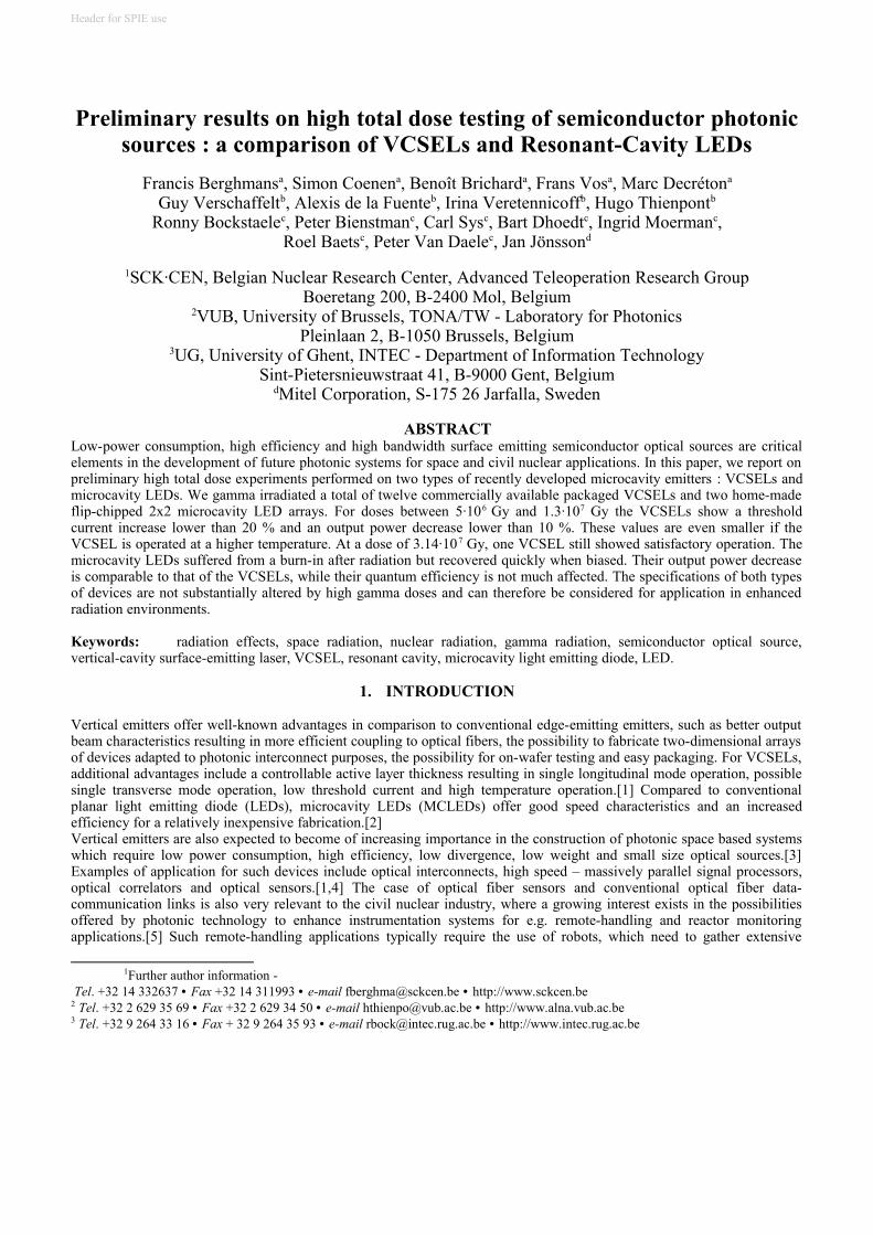
semiconductor, due to the low angle of total internal reflection. As a result, the total efficiency of planar LEDs is under 2 %. In an MCLED, the active region in placed between 2 mirrors. These mirrors act as a Fabry-Perot cavity. Depending on the cavity length and the wavelength, constructive or destructive interference occurs, resulting in an increased or decreased field amplitude at the active region. The amplitude of the electric field at the active region determines the spontaneous emission rates. A well-designed cavity thus alters the emission pattern of the active layer, resulting in LEDs with decreased spectral width, increased extraction efficiency, increased modulation characteristics and/or decreased far field width.The microcavity effect in semiconductor devices has been studied extensively. Schubert et al [23] demonstrated devices at 930 nm. These devices exhibited a narrower FWHM spectrum and showed modulation speeds up to 622 Mbit/s. Deppe et al. [24] demonstrated MCLEDs emitting at 940 nm with an increased 3dB modulation frequency. The microcavity effect was used by De Neve et al. [25] to enchance the extraction efficiency, resulting in record values of 22 % (although this value was partially obtained using the photon recycling principle). In this work, MCLEDs are used that are optimized for coupling to a numerical aperture of 0.5, for guided wave interconnect applications.[26]
E-fieldamplitude
gold mirror p++ GaAs contactlayer
AlGaAs cavity with3 InGaAs QWs
AlAs/GaAs DBR
GaAs substrate
phase matchingGaAs layer
Fig. 1 : Structure of a microcavity light-emitting diode (MCLED)
Fig. 2 : MCLED array flip-chip mounted on a glass substrate
0
0.5
1
1.5
2
2.5
3
3.5
0 5 10 15 20
Injection current (mA)
Out
put
Pow
er (
mW
)
0
0.5
1
1.5
2
2.5
3
3.5
Vol
tage
(V
)
30 µm
40 µm
85 µm
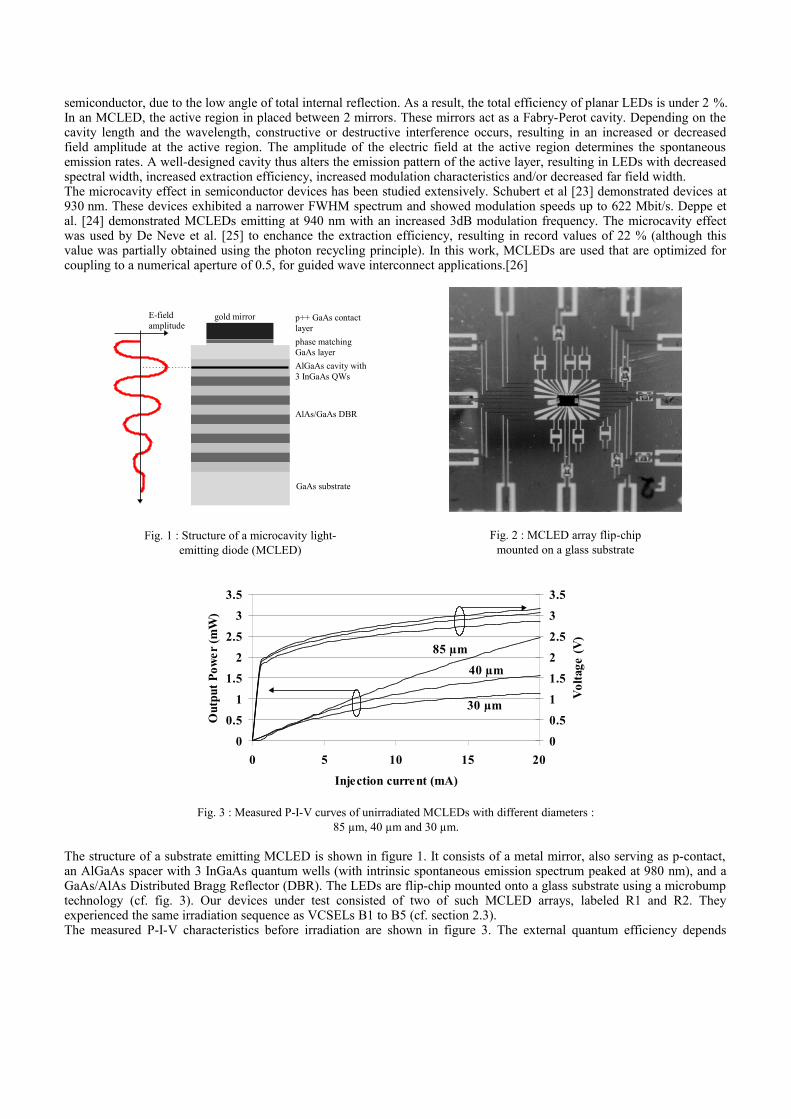
Fig. 3 : Measured P-I-V curves of unirradiated MCLEDs with different diameters :85 µm, 40 µm and 30 µm.
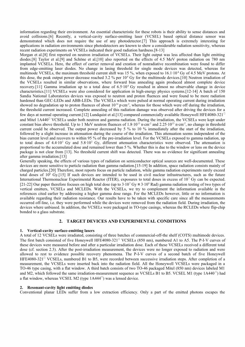
The structure of a substrate emitting MCLED is shown in figure 1. It consists of a metal mirror, also serving as p-contact, an AlGaAs spacer with 3 InGaAs quantum wells (with intrinsic spontaneous emission spectrum peaked at 980 nm), and a GaAs/AlAs Distributed Bragg Reflector (DBR). The LEDs are flip-chip mounted onto a glass substrate using a microbump technology (cf. fig. 3). Our devices under test consisted of two of such MCLED arrays, labeled R1 and R2. They experienced the same irradiation sequence as VCSELs B1 to B5 (cf. section 2.3).The measured P-I-V characteristics before irradiation are shown in figure 3. The external quantum efficiency depends
strongly on the LED diameter. The smallest MCLEDs saturate fast due to thermal effects and carrier overflow. The maximal quantum efficiency is 12% (for 85 µm devices). The smallest MCLEDs show the largest voltage drop.
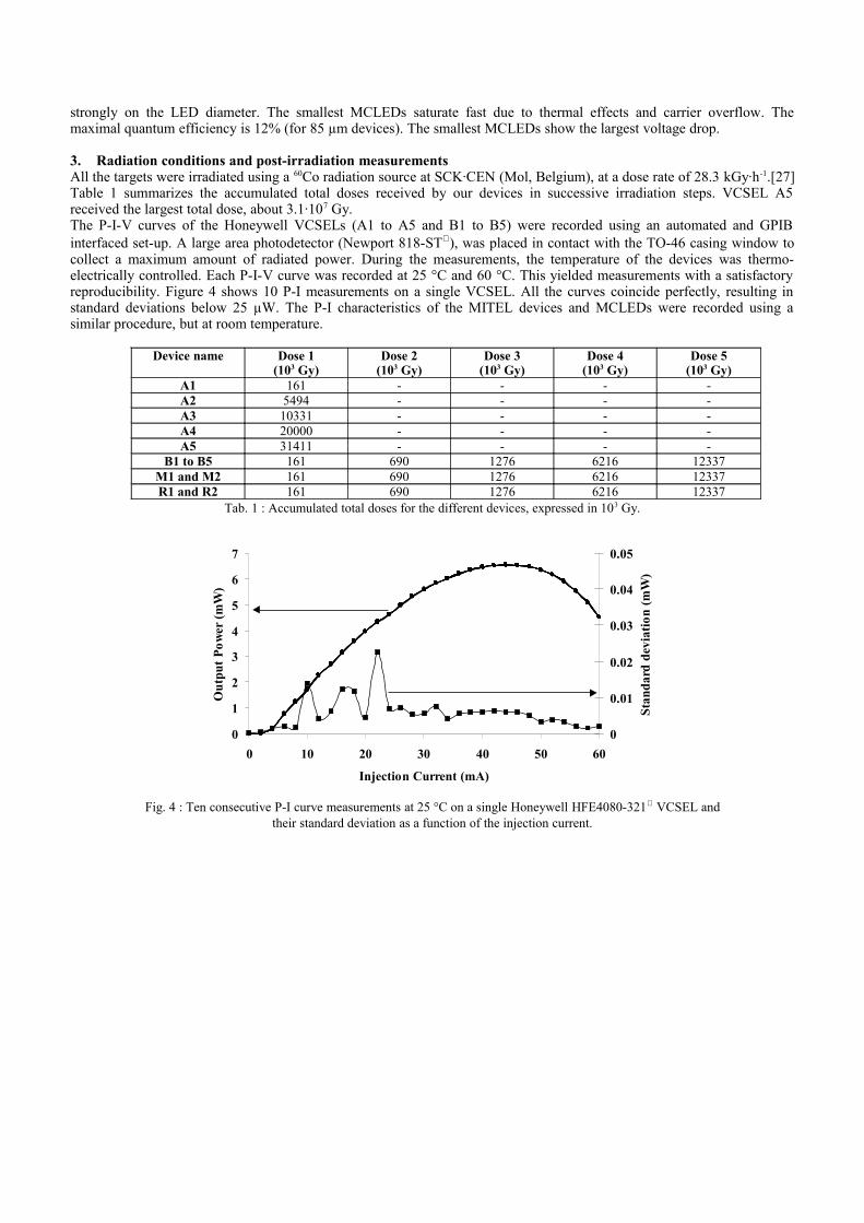
3. Radiation conditions and post-irradiation measurementsAll the targets were irradiated using a 60Co radiation source at SCK·CEN (Mol, Belgium), at a dose rate of 28.3 kGy·h-1.[27] Table 1 summarizes the accumulated total doses received by our devices in successive irradiation steps. VCSEL A5 received the largest total dose, about 3.1·107 Gy.The P-I-V curves of the Honeywell VCSELs (A1 to A5 and B1 to B5) were recorded using an automated and GPIB interfaced set-up. A large area photodetector (Newport 818-ST), was placed in contact with the TO-46 casing window to collect a maximum amount of radiated power. During the measurements, the temperature of the devices was thermo-electrically controlled. Each P-I-V curve was recorded at 25 °C and 60 °C. This yielded measurements with a satisfactory reproducibility. Figure 4 shows 10 P-I measurements on a single VCSEL. All the curves coincide perfectly, resulting in standard deviations below 25 µW. The P-I characteristics of the MITEL devices and MCLEDs were recorded using a similar procedure, but at room temperature.
Device name Dose 1(103 Gy)
Dose 2(103 Gy)
Dose 3(103 Gy)
Dose 4(103 Gy)
Dose 5(103 Gy)
A1 161 - - - -A2 5494 - - - -A3 10331 - - - -A4 20000 - - - -A5 31411 - - - -
B1 to B5 161 690 1276 6216 12337M1 and M2 161 690 1276 6216 12337R1 and R2 161 690 1276 6216 12337
Tab. 1 : Accumulated total doses for the different devices, expressed in 103 Gy.
0
1
2
3
4
5
6
7
0 10 20 30 40 50 60
Injection Current (mA)
Ou
tput
Po
wer
(m
W)
0
0.01
0.02
0.03
0.04
0.05
Sta
ndar
d d
evia
tion
(m
W)
Fig. 4 : Ten consecutive P-I curve measurements at 25 °C on a single Honeywell HFE4080-321 VCSEL and their standard deviation as a function of the injection current.
4. VCSEL RESULTS AND DISCUSSION
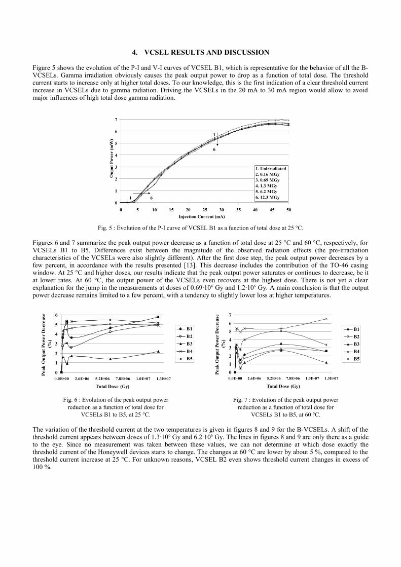
Figure 5 shows the evolution of the P-I and V-I curves of VCSEL B1, which is representative for the behavior of all the B-VCSELs. Gamma irradiation obviously causes the peak output power to drop as a function of total dose. The threshold current starts to increase only at higher total doses. To our knowledge, this is the first indication of a clear threshold current increase in VCSELs due to gamma radiation. Driving the VCSELs in the 20 mA to 30 mA region would allow to avoid major influences of high total dose gamma radiation.
0
1
2
3
4
5
6
7
0 5 10 15 20 25 30 35 40 45 50
Injection Current (mA)
Oup
ut P
ower
(m
W)
1. Unirradiated2. 0.16 MGy3. 0.69 MGy4. 1.3 MGy5. 6.2 MGy6. 12.3 MGy
1
6
1 6
Fig. 5 : Evolution of the P-I curve of VCSEL B1 as a function of total dose at 25 °C.
Figures 6 and 7 summarize the peak output power decrease as a function of total dose at 25 °C and 60 °C, respectively, for VCSELs B1 to B5. Differences exist between the magnitude of the observed radiation effects (the pre-irradiation characteristics of the VCSELs were also slightly different). After the first dose step, the peak output power decreases by a few percent, in accordance with the results presented [13]. This decrease includes the contribution of the TO-46 casing window. At 25 °C and higher doses, our results indicate that the peak output power saturates or continues to decrease, be it at lower rates. At 60 °C, the output power of the VCSELs even recovers at the highest dose. There is not yet a clear explanation for the jump in the measurements at doses of 0.69·106 Gy and 1.2·106 Gy. A main conclusion is that the output power decrease remains limited to a few percent, with a tendency to slightly lower loss at higher temperatures.
0
1
2
3
4
5
6
0.0E+00 2.6E+06 5.2E+06 7.8E+06 1.0E+07 1.3E+07
Total Dose (Gy)
Pea
k O
utpu
t P
ower
Dec
reas
e (%
)
B1
B2
B3
B4
B5
Fig. 6 : Evolution of the peak output power reduction as a function of total dose for
VCSELs B1 to B5, at 25 °C.
0
1
2
3
4
5
6
7
0.0E+00 2.6E+06 5.2E+06 7.8E+06 1.0E+07 1.3E+07
Total Dose (Gy)
Pea
k O
utpu
t P
ower
Dec
reas
e (%
)
B1
B2
B3
B4
B5
Fig. 7 : Evolution of the peak output power reduction as a function of total dose for
VCSELs B1 to B5, at 60 °C.
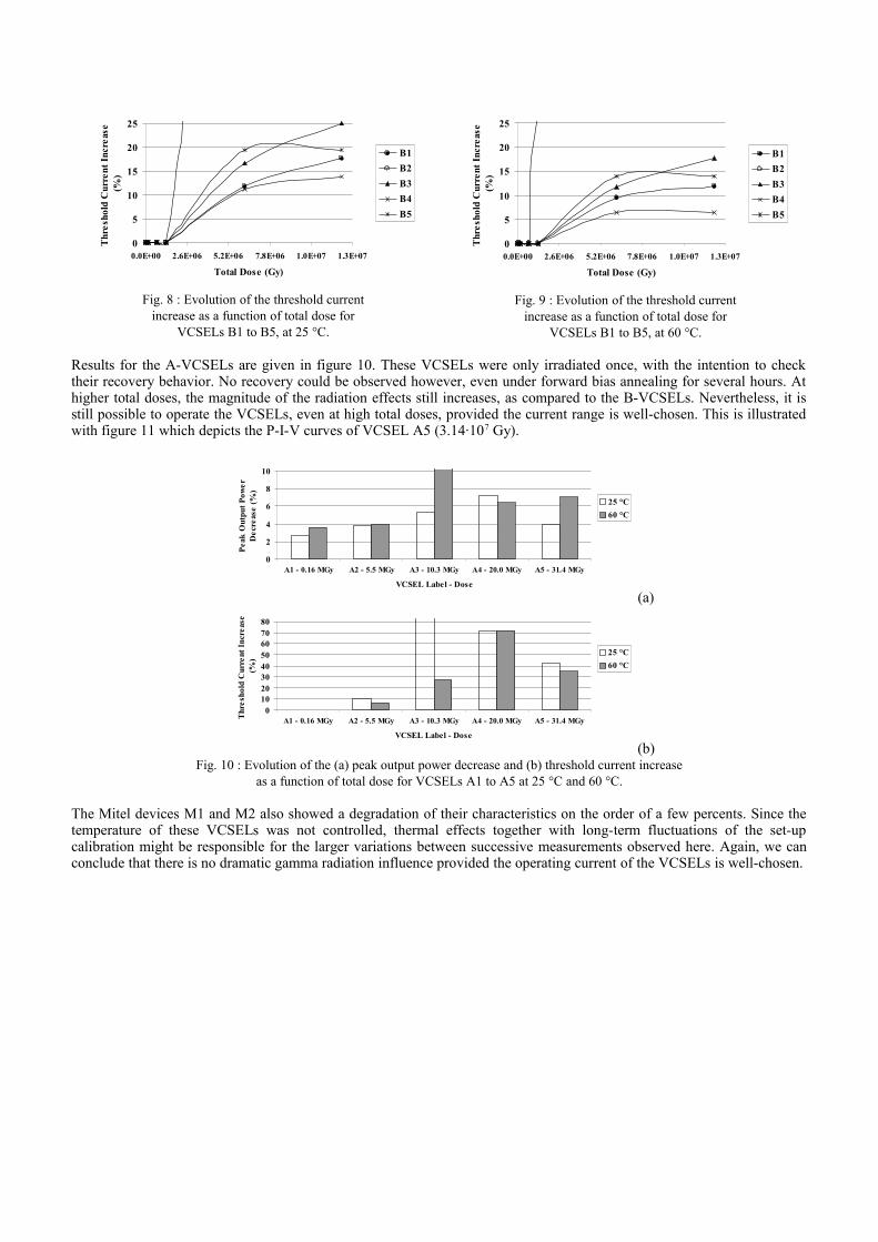
The variation of the threshold current at the two temperatures is given in figures 8 and 9 for the B-VCSELs. A shift of the threshold current appears between doses of 1.3·106 Gy and 6.2·106 Gy. The lines in figures 8 and 9 are only there as a guide to the eye. Since no measurement was taken between these values, we can not determine at which dose exactly the threshold current of the Honeywell devices starts to change. The changes at 60 °C are lower by about 5 %, compared to the threshold current increase at 25 °C. For unknown reasons, VCSEL B2 even shows threshold current changes in excess of 100 %.
0
5
10
15
20
25
0.0E+00 2.6E+06 5.2E+06 7.8E+06 1.0E+07 1.3E+07
Total Dose (Gy)
Thr
esho
ld C
urre
nt I
ncre
ase
(%)
B1
B2
B3
B4
B5
Fig. 8 : Evolution of the threshold current increase as a function of total dose for
VCSELs B1 to B5, at 25 °C.
0
5
10
15
20
25
0.0E+00 2.6E+06 5.2E+06 7.8E+06 1.0E+07 1.3E+07
Total Dose (Gy)
Thr
esho
ld C
urre
nt I
ncre
ase
(%)
B1
B2
B3
B4
B5
Fig. 9 : Evolution of the threshold current increase as a function of total dose for
VCSELs B1 to B5, at 60 °C.
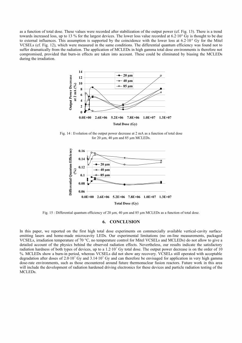
Results for the A-VCSELs are given in figure 10. These VCSELs were only irradiated once, with the intention to check their recovery behavior. No recovery could be observed however, even under forward bias annealing for several hours. At higher total doses, the magnitude of the radiation effects still increases, as compared to the B-VCSELs. Nevertheless, it is still possible to operate the VCSELs, even at high total doses, provided the current range is well-chosen. This is illustrated with figure 11 which depicts the P-I-V curves of VCSEL A5 (3.14·107 Gy).
0
2
4
6
8
10
A1 - 0.16 MGy A2 - 5.5 MGy A3 - 10.3 MGy A4 - 20.0 MGy A5 - 31.4 MGy
VCSEL Label - Dose
Pea
k O
utpu
t P
ower
D
ecre
ase
(%)
25 °C
60 °C
(a)
01020304050607080
A1 - 0.16 MGy A2 - 5.5 MGy A3 - 10.3 MGy A4 - 20.0 MGy A5 - 31.4 MGy
VCSEL Label - Dose
Thr
esho
ld C
urre
nt I
ncre
ase
(%)
25 °C
60 °C
(b)Fig. 10 : Evolution of the (a) peak output power decrease and (b) threshold current increase
as a function of total dose for VCSELs A1 to A5 at 25 °C and 60 °C.
The Mitel devices M1 and M2 also showed a degradation of their characteristics on the order of a few percents. Since the temperature of these VCSELs was not controlled, thermal effects together with long-term fluctuations of the set-up calibration might be responsible for the larger variations between successive measurements observed here. Again, we can conclude that there is no dramatic gamma radiation influence provided the operating current of the VCSELs is well-chosen.

0
1
2
3
4
5
6
7
0 10 20 30 40 50 60
Injection Current (mA)
Out
put
Pow
er (m
W)
0
0.5
1
1.5
2
2.5
3
3.5
Vol
tage
(V
)
Unirradiated
31.4 MGy
Unirradiated
31.4 MGy
Fig. 11 : P-I-V curves of VCSEL A5 before and after 3.14·107 Gy gamma irradiation.
0.0
2.0
4.0
6.0
8.0
10.0
12.0
14.0
16.0
0.0E+00 2.6E+06 5.2E+06 7.8E+06 1.0E+07 1.3E+07
Total Dose (Gy)
Out
put
Pow
er D
ecre
ase
at 1
2 m
A (
%)
0.0
2.0
4.0
6.0
8.0
10.0
12.0
14.0
16.0
Thr
esho
ld C
urre
nt I
ncre
ase
(%)
M1 Power
M2 Power
M1 Threshold
M2 Threshold
Fig. 12 : Evolution of the output power decrease at 12 mA and threshold current increaseas a function of total dose for VCSELs M1 and M2, measured at room temperature.
5. MCLED RESULTS AND DISCUSSION
After an irradiation dose of 6.2·106 Gy, the larger diameter MCLEDs showed a significant ‘burn-in’ period : the optical power increased as function of time and saturated at values proportional to the burn-in current. Figure 13 shows the measured output power as a function of time for 85 µm devices, at 6.2·106 Gy and 1.2·107 Gy. Smaller devices have a much shorter burn-in time. This could be related to thermal effects : smaller devices exhibit higher temperature increase, and thus faster annealing. This behavior contrasts to the VCSELs, with which no recovery could be evidenced.
0
50
100
150
200
250
0 100 200 300 400 500 600
Time (s)
Out
put
Pow
er (
µW
)
6.2 MGy
12.3 MGy
Fig. 13 : Output power of a 85 µm MCLED as a function of time at 6.2·106 Gy and 1.2·107 Gy.
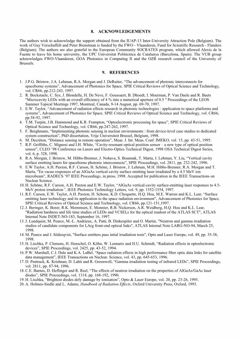
Figures 14 and 15 show the evolution of the MCLED output power and differential quantum efficiency of some MCLEDs
as a function of total dose. These values were recorded after stabilization of the output power (cf. Fig. 13). There is a trend towards increased loss, up to 13 % for the largest devices. The lower loss value recorded at 6.2·106 Gy is thought to be due to external influences. This assumption is supported by the coincidence with the lower loss at 6.2·10 6 Gy for the Mitel VCSELs (cf. Fig. 12), which were measured in the same conditions. The differential quantum efficiency was found not to suffer dramatically from the radiation. The application of MCLEDs in high gamma total dose environments is therefore not compromised, provided that burn-in effects are taken into account. These could be eliminated by biasing the MCLEDs during the irradiation.
0
2
4
6
8
10
12
14
0.0E+00 2.6E+06 5.2E+06 7.8E+06 1.0E+07 1.3E+07
Total Dose (Gy)
Out
put
Pow
er D
ecre
ase
at 2
mA
(%
)20 µm
40 µm
85 µm
Fig. 14 : Evolution of the output power decrease at 2 mA as a function of total dosefor 20 µm, 40 µm and 85 µm MCLEDs.
0.06
0.08
0.1
0.12
0.14
0.16
0.0E+00 2.6E+06 5.2E+06 7.8E+06 1.0E+07 1.3E+07
Total Dose (Gy)
Dif
fere
ntia
l Qua
ntum
Eff
icie
ncy
(%)
20 µm
40 µm
85 µm
Fig. 15 : Differential quantum efficiency of 20 µm, 40 µm and 85 µm MCLEDs as a function of total dose.
6. CONCLUSION
In this paper, we reported on the first high total dose experiments on commercially available vertical-cavity surface-emitting lasers and home-made microcavity LEDs. Our experimental limitations (no on-line measurements, packaged VCSELs, irradiation temperature of 70 °C, no temperature control for Mitel VCSELs and MCLEDs) do not allow to give a detailed account of the physics behind the observed radiation effects. Nevertheless, our results indicate the satisfactory radiation hardness of both types of devices, up to a 1.2·107 Gy total dose. The output power decrease is on the order of 10 %. MCLEDs show a burn-in period, whereas VCSELs did not show any recovery. VCSELs still operated with acceptable degradation after doses of 2.0·107 Gy and 3.14·107 Gy and can therefore be envisaged for application in very high gamma dose-rate environments, such as those encountered around future thermonuclear fusion reactors. Future work in this area will include the development of radiation hardened driving electronics for these devices and particle radiation testing of the MCLEDs.
8. ACKNOWLEDGEMENTS
The authors wish to acknowledge the support obtained from the IUAP-13 Inter-University Attraction Pole (Belgium). The work of Guy Verschaffelt and Peter Bienstman is funded by the FWO - Vlaanderen, Fund for Scientific Research - Flanders (Belgium). The authors are also grateful to the European Community SOCRATES program, which allowed Alexis de la Fuente to leave his home university, the UPC Universitat Politècnica de Catalunya (Barcelona, Spain). The VUB group acknowledges FWO-Vlaanderen, GOA Photonics in Computing II and the OZR research council of the University of Brussels.
9. REFERENCES
1. J.P.G. Bristow, J.A. Lehman, R.A. Morgan and J. DeRuiter, “The advancement of photonic interconnects for spaceborne systems”, Advancement of Photonics for Space, SPIE Critical Reviews of Optical Science and Technology, vol. CR66, pp.212-243, 1997.
2. R. Bockstaele, C. Sys, J. Blondelle, H. De Neve, F. Goussaert, B. Dhoedt, I. Moerman, P. Van Daele and R. Baets "Microcavity LEDs with an overall efficiency of 4 % into a numerical aperture of 0.5 " Proceedings of the LEOS Summer Topical Meetings 1997, Montreal, Canada, 9-14 August, pp. 69-70, 1997.
3. E.W. Taylor, “Advancement of radiation effects research in photonic technologies : application to space platforms and systems”, Advancement of Photonics for Space, SPIE Critical Reviews of Optical Science and Technology, vol. CR66, pp.58-92, 1997.
4. T.M. Turpin, J.B. Hammond and K.R. Frampton, “Optoelectronic processing for space”, SPIE Critical Reviews of Optical Science and Technology, vol. CR66, pp.247-262, 1997.
5. F. Berghmans, “Implementing photonic sensing in nuclear environments : from device-level case studies to dedicated system construction”, PhD dissertation, Vrije Universiteit Brussel, Belgium, 1998.
6. M. Decréton, “Distance sensing in remote operation”, Meas. J. Int. Meas. Conf. IMEKO, vol. 15, pp. 43-51, 1995.7. R.P. Griffiths, C. Mignosi and I.H. White, “Cavity-resonant optical position sensor – a new type of optical position
sensor”, CLEO ’98 Conference on Lasers and Electro-Optics Technical Digest, 1998 OSA Technical Digest Series, vol. 6, p. 328, 1998.
8. R.A. Morgan, J. Bristow, M. Hibbs-Brenner, J. Nohava, S. Bounnak, T. Marta, J. Lehman, Y. Liu, “Vertical cavity surface emitting lasers for spaceborne photonic interconnects”, SPIE Proceedings, vol. 2811, pp. 232-242, 1996.
9. E.W Taylor, A.H. Paxton, R.F. Carson, H. Schöne, J. Bristow, J. Lehman, M.H. Hibbs-Brenner, R.A. Morgan and T. Marta, “En vacuo responses of an AlGaAs vertical cavity surface emitting laser irradiated by a 4.5 MeV ion microbeam”, RADECS ’97 IEEE Proceedings, in press, 1998. Accepted for publication in the IEEE Transactions on Nuclear Science.
10. H. Schöne, R.F. Carson, A.H. Paxton and E.W. Taylor, “AlGaAs vertical-cavity surface-emitting laser responses to 4.5-MeV proton irradiation”, IEEE Photonics Technology Letters, vol. 9, pp. 1552-1554, 1997.
11. R.F. Carson, E.W. Taylor, A.H. Paxton, H. Schone, K.D. Choquette, H.Q. Hou, M.E. Warren and K.L. Lear, “Surface emitting laser technology and its application to the space radiation environment”, Advancement of Photonics for Space, SPIE Critical Reviews of Optical Science and Technology, vol. CR66, pp.121-151,1997.
12. J. Beringer, K. Borer, R.K. Mommsen, E. Monnier, R.B. Nickerson, A.R. Weidberg, H.Q. Hou and K.L. Lear, "Radiation hardness and life time studies of LEDs and VCSELs for the optical readout of the ATLAS SCT", ATLAS Internal Note INDET-NO-183, September 16, 1997.
13. J. Lundquist, M. Pearce, M.-L. Andrieux, A. Patti, B. Dinkespiler and O. Martin, "Neutron and gamma irradiation studies of candidate components for LArg front-end optical links", ATLAS Internal Note LARG-NO-94, March 25, 1998.
14. M. Pearce and J. Söderqvist, "Surface emitters pass intial irradiation tests", Opto and Laser Europe, vol. 49, pp. 35-38, 1998.
15. H. Lischka, P. Clemens, H. Henschel, O. Köhn, W. Lennartz and H.U. Schmidt, “Radiation effects in optoelectronic devices”, SPIE Proceedings, vol. 2425, pp. 43-52, 1994.
16. P.W. Marshall, C.J. Dale and K.A. LaBel, “Space radiation effects in high performance fiber optic data links for satellite data management”, IEEE Transactions on Nuclear. Science, vol. 43, pp. 645-653, 1996.
17. D. Pentrack, K. Krishnan, D. Lahti and R. Greenwell, “Gamma irradiation testing of infrared LEDs”, SPIE Proceedings, vol. 2811, pp. 87-94, 1996.
18. C.E. Barnes, D. Heflinger and R. Reel, “The effects of neutron irradiation on the properties of AlGaAs/GaAs laser diodes”, SPIE Proceedings, vol. 1314, pp. 168-192, 1990.
19. H. Lischka, “Brightest diodes defy damage by ionisation”, Opto & Laser Europe, vol. 20, pp. 23-26, 1995.20. A. Holmes-Siedle and L. Adams, Handbook of Radiation Effects, Oxford University Press, Oxford, 1993.
21. S. Mori, "Irradiation Testing on Standard Components", Working meeting on Irradiation Testing of Standard Components, SCK·CEN, Mol, Belgium, 22-24 May 1996.
22. S.Yamamoto, Combined meeting of neutron and gamma irradiation effects on ITER in-vessel components, ITER-JWS, Garching, Germany, 22-26 June 1998.
23. E. F. Schubert, N. E. J. Hunt, R. J . Malik, M. Micovic and D. L. Miller, "Temperature and Modulation Characteristics of Resonant-Cavity Light-Emitting Dioded", IEEE Journal of Lightwave Technology, vol 14, pp 1721-1728, 1996.
24. D. G. Deppe, J. C. Campbell, R. Kuchibhotla, T. J. Rogers and B. G. Streetman, “Optically-coupled Mirror-Quantum Well InGaAs-GaAs Light Emitting Diode”, Electronics Letter, vol 26, p 1665-1666, 1990.
25. H. De Neve, J. Blondelle, P. Van Daele, P. Demeester, R. Baets and G. Borghs, "Recycling of Guided Mode Light Emission in Planar Microcavity Light Emitting Diodes", Appl. Phys. Lett., vol. 77, p 799-801, 1997.
26. R. Bockstaele, C. Sys, J. Blondelle, B. Dhoedt, I. Moerman, P. Van Daele, P. Demeester and R. Baets, "Resonant Cavity LEDs Optimized for Coupling to Polymer Optical Fibers", accepted for publication in IEEE Photonics Technology Letters.
27. S. Coenen, J. Vermunt, L. Van den Durpel, M. Decréton and A. Rahn, “Gamma Irradiation Facilities for Assessment of Advanced Instrumentation - New Reactor Design and Plant Life Extension Increase their Need”, Research Facilities for the Future of Nuclear Energy, H.A. Abderrahim, Proceedings of an ENS Class 1 Topical Meeting, World Scientific Publishing Co., pp. 382-391, 1996.
Related Documents
![APPLICATION Plasma Processes BRIEF for VCSELs · 2018-07-26 · Geography - Global Forecast to 2022” MarketsandMarkets [3] “Vertical Cavity Surface Emitting Laser (VCSELs) Market](https://static.cupdf.com/doc/110x72/5ed97bd11b54311e7967a587/application-plasma-processes-brief-for-vcsels-2018-07-26-geography-global-forecast.jpg)
![APPLICATION Plasma Processes BRIEF for VCSELs · Geography - Global Forecast to 2022” MarketsandMarkets [3] “Vertical Cavity Surface Emitting Laser (VCSELs) Market - Global Industry](https://static.cupdf.com/doc/110x72/5f9d30cf2e8f9d72ea258e2c/application-plasma-processes-brief-for-vcsels-geography-global-forecast-to-2022a.jpg)


