COMPANY CONFIDENTIAL • 1 Data Sheet © 2010 by Atheros Communications, Inc. All rights reserved. Atheros®, Atheros Driven®, Align®, Atheros XR®, Driving the Wireless Future®, Intellon®, No New Wires®, Orion® , PLC4Trucks®, Powerpacket®, Spread Spectrum Carrier®, SSC®, ROCm®, Super A/G®, Super G®, Super N®, The Air is Cleaner at 5-GHz®, Total 802.11®, U- Nav®, Wake on Wireless®, Wireless Future. Unleashed Now.®, and XSPAN®, are registered by Atheros Communications, Inc. Atheros SST™, Signal-Sustain Technology™, Ethos™, Install N Go™, IQUE™, ROCm™, amp™, Simpli-Fi™, There is Here™, U-Map™, U-Tag™, and 5-UP™ are trademarks of Atheros Communications, Inc. The Atheros logo is a registered trademark of Atheros Communications, Inc. All other trademarks are the property of their respective holders. Subject to change without notice. PRELIMINARY December 2010 AR9331 Highly-Integrated and Cost Effective IEEE 802.11n 1x1 2.4 GHz SoC for AP and Router Platforms General Description The Atheros AR9331 is a highly integrated and cost effective IEEE 802.11n 1x1 2.4 GHz System- on-a-Chip (SoC) for wireless local area network (WLAN) AP and router platforms. In a single chip, the AR9331 includes a MIPS 24K processor, five-port IEEE 802.3 Fast Ethernet Switch with MAC/PHY, one USB 2.0 MAC/PHY, and external memory interface for serial Flash, SDRAM, DDR1 or DDR2, I 2 S/SPDIF-Out audio interface, SLIC VOIP/PCM interface, UART, and GPIOs that can be used for LED controls or other general purpose interface configurations. The AR9331 integrates two Gbit MACs plus a five-port Fast Ethernet switch with a four-traffic class Quality of Service (QoS) engine. The AR9331 integrates an 802.11n 1x1 MAC/BB/ radio with internal PA and LNA. It supports 802.11n operations up to 72 Mbps for 20 MHz and 150 Mbps for 40 MHz channel respectively, and IEEE 802.11b/g data rates. Additional features include on-chip one-time programmable (OTP) memory. Features ■ Complete IEEE 802.11n 1x1 AP or router in a single chip ■ MIPS 24K processor operating at up to 400 MHz ■ External 16-bit DDR1, DDR2, or SDRAM memory interface ■ SPI NOR Flash memory support ■ No external EEPROM needed ■ 4 LAN ports and 1 WAN port IEEE 802.3 Fast Ethernet switch with auto-crossover, auto polarity, and auto-negotiation in PHYs ■ Four classes of QoS per port ■ Fully integrated RF front-end including PA and LNA ■ Optional external LNA/PA ■ Switched antenna diversity ■ High-speed UART for console support ■ I 2 S/SPDIF-out audio interface ■ SLIC for VOIP/PCM ■ USB 2.0 host/device mode support ■ GPIO/LED support ■ JTAG-based processor debugging supported ■ 25 MHz or 40 MHz reference clock input ■ Advanced power management with dynamic clock switching for ultra-low power modes ■ 148-pin, 12 mm x 12 mm dual-row LPCC package System Block Diagram SDRAM/ DDR1/DDR2 Controller and NOR Flash Memory Interface MIPS 24K Processor AR9331 Serial Flash and SDRAM/DDR Interface USB MAC/PHY USB 2.0 Interface 5x Fast Ethernet LAN/WAN Ports 5x Fast Ethernet Ports External Interface GPIOs/LEDs UART UART Interface 2.4 GHz 802.11n 1x1 WLAN MAC/BB/ Radio RF Front End 25 or 40 MHz Crystal I 2 S/SPDIF Audio Interface Internal SRAM I-Cache D-Cache SLIC VOIP/PCM

Welcome message from author
This document is posted to help you gain knowledge. Please leave a comment to let me know what you think about it! Share it to your friends and learn new things together.
Transcript

COMPANY CONFIDENTIAL
Data Sheet
© 2010 by Atheros Communications, Inc. All rights reserved. Atheros®, Atheros Driven®, Align®, Atheros Orion® , PLC4Trucks®, Powerpacket®, Spread Spectrum Carrier®, SSC®, ROCm®, Super A/G®, Super G
Nav®, Wake on Wireless®, Wireless Future. Unleashed Now.®, and XSPAN®, are registered by Atheros CoEthos™, Install N Go™, IQUE™, ROCm™, amp™, Simpli-Fi™, There is Here™, U-Map™, U-Tag™, and
Atheros logo is a registered trademark of Atheros Communications, Inc. All other trademarks are the prope
PRELIMINARYDecember 2010
AR9331 Highly-Integrated and Cost Effective IEEE 802.11n 1x1 2.4 GHz SoC for AP and Router Platforms
General DescriptionThe Atheros AR9331 is a highly integrated and cost effective IEEE 802.11n 1x1 2.4 GHz System-on-a-Chip (SoC) for wireless local area network (WLAN) AP and router platforms.
In a single chip, the AR9331 includes a MIPS 24K processor, five-port IEEE 802.3 Fast Ethernet Switch with MAC/PHY, one USB 2.0 MAC/PHY, and external memory interface for serial Flash, SDRAM, DDR1 or DDR2, I2S/SPDIF-Out audio interface, SLIC VOIP/PCM interface, UART, and GPIOs that can be used for LED controls or other general purpose interface configurations.
The AR9331 integrates two Gbit MACs plus a five-port Fast Ethernet switch with a four-traffic class Quality of Service (QoS) engine.
The AR9331 integrates an 802.11n 1x1 MAC/BB/radio with internal PA and LNA. It supports 802.11n operations up to 72 Mbps for 20 MHz and 150 Mbps for 40 MHz channel respectively, and IEEE 802.11b/g data rates. Additional features include on-chip one-time programmable (OTP) memory.
Features■ Complete IEEE 802.11n 1x1 AP or router in a
single chip■ MIPS 24K processor operating at up to
400 MHz■ External 16-bit DDR1, DDR2, or SDRAM
memory interface■ SPI NOR Flash memory support■ No external EEPROM needed■ 4 LAN ports and 1 WAN port IEEE 802.3 Fast
Ethernet switch with auto-crossover, auto polarity, and auto-negotiation in PHYs
■ Four classes of QoS per port■ Fully integrated RF front-end including PA
and LNA■ Optional external LNA/PA■ Switched antenna diversity■ High-speed UART for console support■ I2S/SPDIF-out audio interface■ SLIC for VOIP/PCM■ USB 2.0 host/device mode support■ GPIO/LED support■ JTAG-based processor debugging supported■ 25 MHz or 40 MHz reference clock input■ Advanced power management with dynamic
clock switching for ultra-low power modes■ 148-pin, 12 mm x 12 mm dual-row LPCC
package
System Block Diagram
SDRAM/DDR1/DDR2
Controller andNOR Flash
MemoryInterface
MIPS 24KProcessorAR9331
Serial Flash and SDRAM/DDR Interface
USB MAC/PHY USB 2.0 Interface
5x Fast EthernetLAN/WAN Ports 5x Fast Ethernet Ports
External Interface GPIOs/LEDs
UART UART Interface
2.4 GHz
802.11n1x1 WLANMAC/BB/
Radio
RFFrontEnd
25 or 40 MHz Crystal
I2S/SPDIF Audio Interface
InternalSRAM
I-CacheD-Cache
SLIC VOIP/PCM
• 1
XR®, Driving the Wireless Future®, Intellon®, No New Wires®, ®, Super N®, The Air is Cleaner at 5-GHz®, Total 802.11®, U-
mmunications, Inc. Atheros SST™, Signal-Sustain Technology™, 5-UP™ are trademarks of Atheros Communications, Inc. The rty of their respective holders. Subject to change without notice.

PRELIMINARY
2 • AR9331 802.11n 1x1 2.4 GHz SoC for AP and Router Platforms Atheros Communications, Inc. 2 • December 2010 COMPANY CONFIDENTIAL
PRELIMINARY
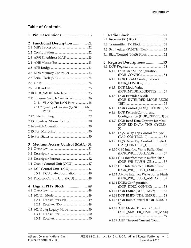
Table of Contents
1 Pin Descriptions .......................... 13
2 Functional Description ............... 212.1 MIPS Processor ....................................... 22
2.2 Configuration ......................................... 22
2.3 AR9331 Address MAP .......................... 23
2.4 AHB Master Bus ..................................... 23
2.5 APB Bridge .............................................. 23
2.6 DDR Memory Controller ...................... 23
2.7 Serial Flash (SPI) .................................... 24
2.8 UART ....................................................... 24
2.9 GE0 and GE1 ........................................... 25
2.10 MDC/MDIO Interface ......................... 25
2.11 Ethernet Switch Controller .................. 262.11.1 VLANs For LAN Ports ............... 282.11.2 Quality of Service (QoS) for LAN
Ports .............................................. 29
2.12 Rate Limiting ......................................... 29
2.13 Broadcast Storm Control ...................... 30
2.14 Switch Operation .................................. 30
2.15 Port Mirroring ....................................... 30
2.16 Port States ............................................... 30
3 Medium Access Control (MAC) 313.1 Overview ................................................. 31
3.2 Descriptor ................................................ 31
3.3 Descriptor Format .................................. 32
3.4 Queue Control Unit (QCU) .................. 47
3.5 DCF Control Unit (DCU) ...................... 473.5.1 DCU State Information .............. 48
3.6 Protocol Control Unit (PCU) ................ 48
4 Digital PHY Block ....................... 494.1 Overview ................................................. 49
4.2 802.11n Mode .......................................... 494.2.1 Transmitter (Tx) .......................... 494.2.2 Receiver (Rx) ............................... 49
4.3 802.11b/g Legacy Mode ........................ 504.3.1 Transmitter .................................. 504.3.2 Receiver ........................................ 50
5 Radio Block ...................................515.1 Receiver (Rx) Block ................................ 51
5.2 Transmitter (Tx) Block .......................... 51
5.3 Synthesizer (SYNTH) Block ................. 52
5.4 Bias/Control (BIAS) Block ................... 52
6 Register Descriptions ..................536.1 DDR Registers ........................................ 54
6.1.1 DRR DRAM Configuration (DDR_CONFIG) ......................... 54
6.1.2 DDR DRAM Configuration 2 (DDR_CONFIG2) ....................... 55
6.1.3 DDR Mode Value (DDR_MODE_REGISTER) ........ 55
6.1.4 DDR Extended Mode (DDR_EXTENDED_MODE_REGISTER) .............................................. 55
6.1.5 DDR Control (DDR_CONTROL) 566.1.6 DDR Refresh Control and
Configuration (DDR_REFRESH) 566.1.7 DDR Read Data Capture Bit Mask
(DDR_RD_DATA_THIS_CYCLE) 56
6.1.8 DQS Delay Tap Control for Byte 0 (TAP_CONTROL_0) .................. 56
6.1.9 DQS Delay Tap Control for Byte 1 (TAP_CONTROL_1) .................. 57
6.1.10 GE0 Interface Write Buffer Flush (DDR_WB_FLUSH_GE0) .......... 57
6.1.11 GE1 Interface Write Buffer Flush (DDR_WB_FLUSH_GE1) .......... 57
6.1.12 USB Interface Write Buffer Flush (DDR_WB_FLUSH_USB) .......... 57
6.1.13 AMBA Interface Write Buffer Flush (DDR_WB_FLUSH_AMBA) ..... 58
6.1.14 DDR2 Configuration (DDR_DDR2_CONFIG) ............. 58
6.1.15 DDR EMR2 (DDR_EMR2) ......... 586.1.16 DDR EMR3 (DDR_EMR3) ......... 586.1.17 DDR Burst Control (DDR_BURST)
596.1.18 AHB Master Timeout Control
(AHB_MASTER_TIMEOUT_MAX) ....................................................... 59
6.1.19 AHB Timeout Current Count
Atheros Communications, Inc. AR9331 802.11n 1x1 2.4 GHz SoC for AP and Router Platforms • 1 COMPANY CONFIDENTIAL December 2010 • 1
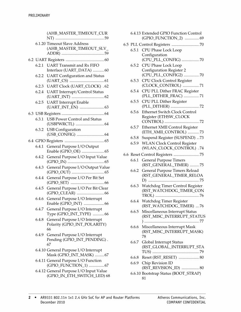
PRELIMINARY
(AHB_MASTER_TIMEOUT_CURNT) ................................................ 59
6.1.20 Timeout Slave Address (AHB_MASTER_TIMEOUT_SLV_ADDR) .......................................... 59
6.2 UART Registers ...................................... 606.2.1 UART Transmit and Rx FIFO
Interface (UART_DATA) ........... 606.2.2 UART Configuration and Status
(UART_CS) .................................. 616.2.3 UART Clock (UART_CLOCK) . 626.2.4 UART Interrupt/Control Status
(UART_INT) ................................ 626.2.5 UART Interrupt Enable
(UART_INT_EN) ........................ 63
6.3 USB Registers .......................................... 646.3.1 USB Power Control and Status
(USBPWRCTL) ............................ 646.3.2 USB Configuration
(USB_CONFIG) ........................... 64
6.4 GPIO Registers ....................................... 656.4.1 General Purpose I/O Output
Enable (GPIO_OE) ...................... 656.4.2 General Purpose I/O Input Value
(GPIO_IN) .................................... 656.4.3 General Purpose I/O Output Value
(GPIO_OUT) ................................ 656.4.4 General Purpose I/O Per Bit Set
(GPIO_SET) ................................. 666.4.5 General Purpose I/O Per Bit Clear
(GPIO_CLEAR) ........................... 666.4.6 General Purpose I/O Interrupt
Enable (GPIO_INT) .................... 666.4.7 General Purpose I/O Interrupt
Type (GPIO_INT_TYPE) ........... 666.4.8 General Purpose I/O Interrupt
Polarity (GPIO_INT_POLARITY) 66
6.4.9 General Purpose I/O Interrupt Pending (GPIO_INT_PENDING) .67
6.4.10 General Purpose I/O Interrupt Mask (GPIO_INT_MASK) ......... 67
6.4.11 General Purpose I/O Function (GPIO_FUNCTION_1) ............... 67
6.4.12 General Purpose I/O Input Value (GPIO_IN_ETH_SWITCH_LED) 68
6.4.13 Extended GPIO Function Control (GPIO_FUNCTION_2) .............. 69
6.5 PLL Control Registers ........................... 706.5.1 CPU Phase Lock Loop
Configuration (CPU_PLL_CONFIG) ................. 70
6.5.2 CPU Phase Lock Loop Configuration Register 2 (CPU_PLL_CONFIG2) ............... 70
6.5.3 CPU Clock Control Register (CLOCK_CONTROL) ................ 71
6.5.4 CPU PLL Dither FRAC Register (PLL_DITHER_FRAC) ............... 71
6.5.5 CPU PLL Dither Register (PLL_DITHER) ............................ 72
6.5.6 Ethernet Switch Clock Control Register (ETHSW_CLOCK CONTROL) .................................. 72
6.5.7 Ethernet XMII Control Register (ETH_XMII_CONTROL) ........... 73
6.5.8 Suspend Register (SUSPEND) .. 736.5.9 WLAN Clock Control Register
(WLAN_CLOCK_CONTROL) . 74
6.6 Reset Control Registers ......................... 756.6.1 General Purpose Timers
(RST_GENERAL_TIMER) ......... 756.6.2 General Purpose Timers Reload
(RST_GENERAL_TIMER_RELOAD) .................................................. 75
6.6.3 Watchdog Timer Control Register (RST_WATCHDOG_TIMER_CONTROL) ........................................... 76
6.6.4 Watchdog Timer Register (RST_WATCHDOG_TIMER) ... 76
6.6.5 Miscellaneous Interrupt Status (RST_MISC_INTERRUPT_STATUS) ...................................................... 77
6.6.6 Miscellaneous Interrupt Mask (RST_MISC_INTERRUPT_MASK) 78
6.6.7 Global Interrupt Status (RST_GLOBAL_INTERRUPT_STATUS) .............................................. 79
6.6.8 Reset (RST_RESET) .................... 806.6.9 Chip Revision ID
(RST_REVISION_ID) ................. 806.6.10 Bootstrap Status (BOOT_STRAP)
81
2 • AR9331 802.11n 1x1 2.4 GHz SoC for AP and Router Platforms Atheros Communications, Inc. 2 • December 2010 COMPANY CONFIDENTIAL
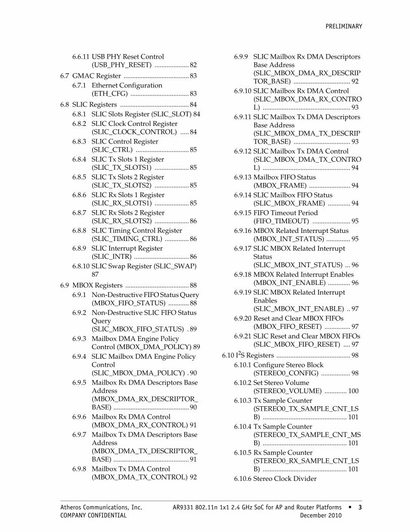
PRELIMINARY
6.6.11 USB PHY Reset Control (USB_PHY_RESET) .................... 82
6.7 GMAC Register ...................................... 836.7.1 Ethernet Configuration
(ETH_CFG) .................................. 83
6.8 SLIC Registers ........................................ 846.8.1 SLIC Slots Register (SLIC_SLOT) 846.8.2 SLIC Clock Control Register
(SLIC_CLOCK_CONTROL) ..... 846.8.3 SLIC Control Register
(SLIC_CTRL) ............................... 856.8.4 SLIC Tx Slots 1 Register
(SLIC_TX_SLOTS1) .................... 856.8.5 SLIC Tx Slots 2 Register
(SLIC_TX_SLOTS2) .................... 856.8.6 SLIC Rx Slots 1 Register
(SLIC_RX_SLOTS1) .................... 856.8.7 SLIC Rx Slots 2 Register
(SLIC_RX_SLOTS2) .................... 866.8.8 SLIC Timing Control Register
(SLIC_TIMING_CTRL) .............. 866.8.9 SLIC Interrupt Register
(SLIC_INTR) ................................ 866.8.10 SLIC Swap Register (SLIC_SWAP)
87
6.9 MBOX Registers ..................................... 886.9.1 Non-Destructive FIFO Status Query
(MBOX_FIFO_STATUS) ............ 886.9.2 Non-Destructive SLIC FIFO Status
Query (SLIC_MBOX_FIFO_STATUS) . 89
6.9.3 Mailbox DMA Engine Policy Control (MBOX_DMA_POLICY) 89
6.9.4 SLIC Mailbox DMA Engine Policy Control (SLIC_MBOX_DMA_POLICY) . 90
6.9.5 Mailbox Rx DMA Descriptors Base Address (MBOX_DMA_RX_DESCRIPTOR_BASE) ............................................ 90
6.9.6 Mailbox Rx DMA Control (MBOX_DMA_RX_CONTROL) 91
6.9.7 Mailbox Tx DMA Descriptors Base Address (MBOX_DMA_TX_DESCRIPTOR_BASE) ............................................ 91
6.9.8 Mailbox Tx DMA Control (MBOX_DMA_TX_CONTROL) 92
6.9.9 SLIC Mailbox Rx DMA Descriptors Base Address (SLIC_MBOX_DMA_RX_DESCRIPTOR_BASE) ................................. 92
6.9.10 SLIC Mailbox Rx DMA Control (SLIC_MBOX_DMA_RX_CONTROL) ................................................... 93
6.9.11 SLIC Mailbox Tx DMA Descriptors Base Address (SLIC_MBOX_DMA_TX_DESCRIPTOR_BASE) ................................. 93
6.9.12 SLIC Mailbox Tx DMA Control (SLIC_MBOX_DMA_TX_CONTROL) ................................................... 94
6.9.13 Mailbox FIFO Status (MBOX_FRAME) ........................ 94
6.9.14 SLIC Mailbox FIFO Status (SLIC_MBOX_FRAME) ............. 94
6.9.15 FIFO Timeout Period (FIFO_TIMEOUT) ...................... 95
6.9.16 MBOX Related Interrupt Status (MBOX_INT_STATUS) .............. 95
6.9.17 SLIC MBOX Related Interrupt Status (SLIC_MBOX_INT_STATUS) ... 96
6.9.18 MBOX Related Interrupt Enables (MBOX_INT_ENABLE) ............. 96
6.9.19 SLIC MBOX Related Interrupt Enables (SLIC_MBOX_INT_ENABLE) .. 97
6.9.20 Reset and Clear MBOX FIFOs (MBOX_FIFO_RESET) ............... 97
6.9.21 SLIC Reset and Clear MBOX FIFOs (SLIC_MBOX_FIFO_RESET) .... 97
6.10 I2S Registers ........................................... 986.10.1 Configure Stereo Block
(STEREO0_CONFIG) ................. 986.10.2 Set Stereo Volume
(STEREO0_VOLUME) ............. 1006.10.3 Tx Sample Counter
(STEREO0_TX_SAMPLE_CNT_LSB) ................................................. 101
6.10.4 Tx Sample Counter (STEREO0_TX_SAMPLE_CNT_MSB) ................................................. 101
6.10.5 Rx Sample Counter (STEREO0_RX_SAMPLE_CNT_LSB) ................................................. 101
6.10.6 Stereo Clock Divider
Atheros Communications, Inc. AR9331 802.11n 1x1 2.4 GHz SoC for AP and Router Platforms • 3 COMPANY CONFIDENTIAL December 2010 • 3

PRELIMINARY
(STEREO_CLOCK_DIV) .......... 101
6.11 MDIO Slave Registers ........................ 1026.11.1 MDIO Handshaking Register 0
(MDIO_HS_REG0) ................... 1026.11.2 MDIO Handshaking Register 1
(MDIO_HS_REG1) ................... 1026.11.3 MDIO Handshaking Register 2
(MDIO_HS_REG2) ................... 1036.11.4 MDIO Handshaking Register 3
(MDIO_HS_REG3) ................... 1036.11.5 MDIO Handshaking Register 4
(MDIO_HS_REG4) ................... 1036.11.6 MDIO Handshaking Register 5
(MDIO_HS_REG5) ................... 1036.11.7 MDIO Handshaking Register 6
(MDIO_HS_REG6) ................... 1046.11.8 MDIO Handshaking Register 7
(MDIO_HS_REG7) ................... 1046.11.9 MDIO ISR Register
(MDIO_ISR_REG) ..................... 104
6.12 General DMA and Rx-Related Registers 1056.12.1 Command (CR) ......................... 1066.12.2 Configuration and Status (CFG) ...
1076.12.3 Rx DMA Data Buffer Pointer
Threshold (RXBUFPTR_THRESH) 108
6.12.4 Tx DMA Descriptor Pointer Threshold (TXDPPTR_THRESH) .108
6.12.5 Maximum Interrupt Rate Threshold (MIRT) ........................................ 108
6.12.6 Interrupt Global Enable (IER) . 1096.12.7 Tx Interrupt Mitigation Thresholds
(TIMT) ........................................ 1096.12.8 Rx Interrupt Mitigation Thresholds
(RIMT) ........................................ 1096.12.9 Tx Configuration (TXCFG) ...... 1106.12.10 Rx Configuration (RXCFG) ... 1106.12.11 MIB Control (MIBC) ............... 1116.12.12 Timeout Prescale (TOPS) ....... 1116.12.13 Global Tx Timeout (GTT) ...... 1116.12.14 Global Tx Timeout Mode (GTTM)
1116.12.15 Carrier Sense Timeout (CST) . 1126.12.16 Size of High and Low Priority
(RXDP_SIZE) ............................. 1126.12.17 MAC Rx High Priority Queue
RXDP Pointer (RX_QUEUE_HP_RXDP) ........ 112
6.12.18 MAC Rx Low Priority Queue RXDP Pointer (RX_QUEUE_LP_RXDP) ......... 112
6.12.19 Primary Interrupt Status (ISR_P) 113
6.12.20 Secondary Interrupt Status 0 (ISR_S0) ...................................... 114
6.12.21 Secondary Interrupt Status 1 (ISR_S1) ...................................... 114
6.12.22 Secondary Interrupt Status 2 (ISR_S2) ...................................... 115
6.12.23 Secondary Interrupt Status 3 (ISR_S3) ...................................... 116
6.12.24 Secondary Interrupt Status 4 (ISR_S4) ...................................... 116
6.12.25 Secondary Interrupt Status 5 (ISR_S5) ...................................... 116
6.12.26 Primary Interrupt Mask (IMR_P) 117
6.12.27 Secondary Interrupt Mask 0 (IMR_S0) .................................... 118
6.12.28 Secondary Interrupt Mask 1 (IMR_S1) .................................... 118
6.12.29 Secondary Interrupt Mask 2 (IMR_S2) .................................... 119
6.12.30 Secondary Interrupt Mask 3 (IMR_S3) .................................... 120
6.12.31 Secondary Interrupt Mask 4 (IMR_S4) .................................... 120
6.12.32 Secondary Interrupt Mask 5 (IMR_S5) .................................... 121
6.12.33 Primary Interrupt Status Read and Clear (ISR_P_RAC) ................... 121
6.12.34 Secondary Interrupt Status 0 (ISR_S0_S) .................................. 121
6.12.35 Secondary Interrupt Status 1 (ISR_S1_S) .................................. 122
6.12.36 Secondary Interrupt Status 2 (ISR_S2_S) .................................. 122
6.12.37 Secondary Interrupt Status 3 (ISR_S3_S) .................................. 122
6.12.38 Secondary Interrupt Status 4 (ISR_S4_S) .................................. 122
6.12.39 Secondary Interrupt Status 5
4 • AR9331 802.11n 1x1 2.4 GHz SoC for AP and Router Platforms Atheros Communications, Inc. 4 • December 2010 COMPANY CONFIDENTIAL
PRELIMINARY
(ISR_S5_S) .................................. 122
6.13 QCU Registers ..................................... 1256.13.1 Tx Queue Descriptor (Q_TXDP) ...
1256.13.2
QCU_STATUS_RING_START_ADDRESS Lower 32 bits of Address (Q_STATUS_RING_START) ... 126
6.13.3 QCU_STATUS_RING_END_ADDR Lower 32 Bits of Address (Q_STATUS_RING_END) ....... 126
6.13.4 QCU_STATUS_RING_CURRENT Address (Q_STATUS_RING_CURRENT) ..126
6.13.5 Tx Queue Enable (Q_TXE) ...... 1266.13.6 Tx Queue Disable (Q_TXD) .... 1276.13.7 CBR Configuration (Q_CBRCFG)
1276.13.8 ReadyTime Configuration
(Q_RDYTIMECFG) ................... 1276.13.9 OneShotArm Set Control
(Q_ONESHOTARM_SC) ......... 1286.13.10 OneShotArm Clear Control
(Q_ONESHOTARM_CC) ........ 1286.13.11 Misc. QCU Settings (Q_MISC) 1296.13.12 Misc. QCU Status (Q_STS) ..... 1316.13.13 ReadyTimeShutdown Status
(Q_RDYTIMESHDN) ............... 1316.13.14 Descriptor CRC Check
(MAC_QCU_DESC_CRC_CHK) ..131
6.14 DCU Registers ..................................... 1326.14.1 QCU Mask (D_QCUMASK) .... 1326.14.2 DCU-Specific IFS Settings
(D_LCL_IFS) .............................. 1336.14.3 Retry Limits (D_RETRY_LIMIT) ..
1336.14.4 ChannelTime Settings
(D_CHNTIME) .......................... 1346.14.5 Misc. DCU-Specific Settings
(D_MISC) ................................... 1346.14.6 DCU-Global IFS Settings: SIFS
Duration (D_GBL_IFS_SIFS) ... 1356.14.7 DCU-Global IFS Settings: Slot
Duration (D_GBL_IFS_SLOT) 1356.14.8 DCU-Global IFS Settings: EIFS
Duration (D_GBL_IFS_EIFS) .. 1356.14.9 DCU-Global IFS Settings: Misc.
Parameters (D_GBL_IFS_MISC) ..136
6.14.10 DCU Tx Pause Control/Status (D_TXPSE) ................................. 136
6.14.11 DCU Transmission Slot Mask (D_TXSLOTMASK) .................. 137
6.15 Host Interface Registers ..................... 1386.15.1 Reset the Host Interface
(HOST_INTF_RESET_CONTROL) 139
6.15.2 Host Timeout (HOST_INTF_TIMEOUT) ....... 139
6.15.3 EEPROM Control (HOST_INTF_EEPROM_CTRL) ..139
6.15.4 MAC Silicon Revision ID (HOST_INTF_SREV) ................ 139
6.15.5 Synchronous Interrupt Cause (HOST_INTF_INTR_SYNC_CAUSE) ................................................. 141
6.15.6 Synchronous Interrupt Enable (HOST_INTF_INTR_SYNC_ENABLE) ............................................... 141
6.15.7 Asynchronous Interrupt Mask (HOST_INTF_INTR_ASYNC_MASK) ................................................. 142
6.15.8 Synchronous Interrupt Mask (HOST_INTF_INTR_SYNC_MASK) ................................................... 142
6.15.9 Asynchronous Interrupt Cause (HOST_INTF_INTR_ASYNC_CAUSE) ............................................... 142
6.15.10 Asynchronous Interrupt Enable (HOST_INTF_INTR_ASYNC_ENABLE) ............................................ 142
6.15.11 GPIO Output (HOST_INTF_GPIO_OUT) ..... 143
6.15.12 GPIO Input (HOST_INTF_GPIO_IN) ......... 143
6.15.13 Host GPIO Output Enable Bits (HOST_INTF_GPIO_OE) ........ 144
6.15.14 Host GPIO Interrupt Polarity (HOST_INTF_GPIO_INTR_POLAR) ................................................... 144
6.15.15 GPIO Input Enable and Value (HOST_INTF_GPIO_INPUT_VALUE) .............................................. 145
Atheros Communications, Inc. AR9331 802.11n 1x1 2.4 GHz SoC for AP and Router Platforms • 5 COMPANY CONFIDENTIAL December 2010 • 5

PRELIMINARY
6.15.16 GPIO Input MUX1 (HOST_INTF_GPIO_INPUT_MUX1) .................................................. 146
6.15.17 GPIO Input MUX2 (HOST_INTF_GPIO_INPUT_MUX2) .................................................. 146
6.15.18 GPIO Output MUX1 (HOST_INTF_GPIO_OUTPUT_MUX1) ............................................... 147
6.15.19 GPIO Output MUX2 (HOST_INTF_GPIO_OUTPUT_MUX2) ............................................... 147
6.15.20 GPIO Output MUX3 (HOST_INTF_GPIO_OUTPUT_MUX3) ............................................... 147
6.15.21 Input Values (HOST_INTF_GPIO_INPUT_STATE) ................................................. 148
6.15.22 EEPROM Status and Read Data (HOST_INTF_EEPROM_STS) 148
6.15.23 RFSilent-Related Registers (HOST_INTF_RFSILENT) ....... 148
6.15.24 GPIO Pull-Up/Pull-Down (HOST_INTF_GPIO_PDPU) ... 149
6.15.25 Synchronous Priority Interrupt Cause (HOST_INTF_INTR_PRIORITY_SYNC_CAUSE) .............................. 149
6.15.26 Synchronous Priority Interrupt Enable (HOST_INTF_INTR_PRIORITY_SYNC_ENABLE) ........................... 149
6.15.27 Asynchronous Priority Interrupt Mask (HOST_INTF_INTR_PRIORITY_ASYNC_MASK) ........................... 150
6.15.28 Synchronous Priority Interrupt Mask (HOST_INTF_INTR_PRIORITY_SYNC_MASK) ................................ 150
6.15.29 Asynchronous Priority Interrupt Cause (HOST_INTF_INTR_PRIORITY_ASYNC_CAUSE) ......................... 150
6.15.30 Asynchronous Priority Interrupt Enable (HOST_INTF_INTR_PRIORITY_ASYNC_ENABLE) ....................... 151
6.16 RTC Interface Registers ...................... 151
6.16.1 PLL Frequency Control Signals Register ...................................... 152
6.16.1 RTC Reset and Force Sleep and Force Wakeup (RTC_RESET) . 152
6.16.2 RTC Sleep Status (RTC_STATUS) 152
6.16.3 RTC Force Derived RTC and Bypass Derived RTC (RTC_DERIVED) 153
6.16.4 RTC Force Wake (RTC_FORCE_WAKE) ............ 153
6.16.5 RTC Interrupt Cause (RTC_INT_CAUSE) .................. 154
6.16.6 RTC Interrupt Cause Clear (RTC_CAUSE_CLR) ................. 154
6.16.7 RTC Interrupt Enable (RTC_INT_ENABLE) ............... 155
6.16.8 RTC Interrupt Mask (RTC_INT_MASK) ................... 155
6.17 MAC PCU Registers ........................... 1566.17.1 STA Address Lower 32 Bits
(MAC_PCU_STA_ADDR_L32) 1596.17.2 STA Address Upper 16 Bits
(MAC_PCU_STA_ADDR_U16) 1596.17.3 BSSID Lower 32 Bits
(MAC_PCU_BSSID_L32) ......... 1606.17.4 BSSID Upper 16 Bits
(MAC_PCU_BSSID_U16) ........ 1606.17.5 Beacon RSSI Average
(MAC_PCU_BCN_RSSI_AVE) 1606.17.6 ACK and CTS Timeout
(MAC_PCU_ACK_CTS_TIMEOUT) .................................................... 160
6.17.7 Beacon RSSI Control (MAC_PCU_BCN_RSSI_CTL) 161
6.17.8 Ms Counter and Rx/Tx Latency (MAC_PCU_USEC_LATENCY) ..161
6.17.9 Reset TSF (MAC_PCU_RESET_TSF) ....... 161
6.17.10 Maximum CFP Duration (MAC_PCU_MAX_CFP_DUR) 162
6.17.11 Rx Filter (MAC_PCU_RX_FILTER) ....... 162
6.17.12 Multicast Filter Mask Lower 32 Bits (MAC_PCU_MCAST_FILTER_L32) ..................................................... 163
6.17.13 Multicast Filter Mask Upper 32 Bits (MAC_PCU_MCAST_FILTER_U32
6 • AR9331 802.11n 1x1 2.4 GHz SoC for AP and Router Platforms Atheros Communications, Inc. 6 • December 2010 COMPANY CONFIDENTIAL

PRELIMINARY
) .................................................... 1636.17.14 Diagnostic Switches
(MAC_PCU_DIAG_SW) .......... 1636.17.15 TSF Lower 32 Bits
(MAC_PCU_TSF_L32) ............. 1646.17.16 TSF Upper 32 Bits
(MAC_PCU_TSF_U32) ............ 1646.17.17 AES Mute Mask 0
(MAC_PCU_AES_MUTE_MASK_0) .................................................... 164
6.17.18 AES Mute Mask 1...........................(MAC_PCU_AES_MUTE_MASK_1) .................................................... 165
6.17.19 Last Rx Beacon TSF (MAC_PCU_LAST_BEACON_TSF) ..................................................... 165
6.17.20 Current NAV (MAC_PCU_NAV) 165
6.17.21 Successful RTS Count (MAC_PCU_RTS_SUCCESS_CNT) 165
6.17.22 Failed RTS Count (MAC_PCU_RTS_FAIL_CNT) 165
6.17.23 FAIL ACK Count (MAC_PCU_ACK_FAIL_CNT) 166
6.17.24 Failed FCS Count (MAC_PCU_FCS_FAIL_CNT) 166
6.17.25 Beacon Count (MAC_PCU_BEACON_CNT) 166
6.17.26 Sleep 1 (MAC_PCU_SLP1) .... 1666.17.27 Sleep 2 (MAC_PCU_SLP2) .... 1676.17.28 Address 1 Mask Lower 32 Bits
(MAC_PCU_ADDR1_MASK_L32) 167
6.17.29 Address 1 Mask Upper 16 Bits (MAC_PCU_ADDR1_MASK_U16) 167
6.17.30 Tx Power Control (MAC_PCU_TPC) ..................... 167
6.17.31 Tx Frame Counter (MAC_PCU_TX_FRAME_CNT) ..168
6.17.32 Rx Frame Counter (MAC_PCU_RX_FRAME_CNT) ..168
6.17.33 Rx Clear Counter (MAC_PCU_RX_CLEAR_CNT) 168
6.17.34 Cycle Counter
(MAC_PCU_CYCLE_CNT) .... 1686.17.35 Quiet Time 1
(MAC_PCU_QUIET_TIME_1) 1686.17.36 Quiet Time 2
(MAC_PCU_QUIET_TIME_2) 1696.17.37 QoS NoACK
(MAC_PCU_QOS_NO_ACK) 1696.17.38 PHY Error Mask
(MAC_PCU_PHY_ERROR_MASK) ..................................................... 170
6.17.39 Rx Buffer (MAC_PCU_RXBUF) .170
6.17.40 QoS Control (MAC_PCU_MIC_QOS_CONTROL) ................................................. 171
6.17.41 Michael QoS Select (MAC_PCU_MIC_QOS_SELECT) 171
6.17.42 Miscellaneous Mode (MAC_PCU_MISC_MODE) .... 172
6.17.43 Filtered OFDM Counter (MAC_PCU_FILTER_OFDM_CNT) ..................................................... 173
6.17.44 Filtered CCK Counter (MAC_PCU_Filter_CCK_CNT) 173
6.17.45 PHY Error Counter 1 (MAC_PCU_PHY_ERR_CNT_1) .173
6.17.46 PHY Error Counter 1 Mask (MAC_PCU_PHY_ERR_CNT_1_MASK) ........................................... 174
6.17.47 PHY Error Counter 2 (MAC_PCU_PHY_ERR_CNT_2) .174
6.17.48 PHY Error Counter 2 Mask (MAC_PCU_PHY_ERR_CNT_2_MASK) ........................................... 174
6.17.49 TSF Threshold (MAC_PCU_TSF_THRESHOLD) 175
6.17.50 PHY Error EIFS Mask (MAC_PCU_PHY_ERROR_EIFS_MASK) ........................................ 175
6.17.51 PHY Error Counter 3 (MAC_PCU_PHY_ERR_CNT_3) .175
6.17.52 PHY Error Counter 3 Mask (MAC_PCU_PHY_ERR_CNT_3_MASK) ........................................... 175
Atheros Communications, Inc. AR9331 802.11n 1x1 2.4 GHz SoC for AP and Router Platforms • 7 COMPANY CONFIDENTIAL December 2010 • 7
PRELIMINARY
6.17.53 Bluetooth Mode (MAC_PCU_BLUETOOTH_MODE) .................................................... 176
6.17.54 Bluetooth WL_LEVEL (MAC_PCU_BLUETOOTH_WL_WEIGHTS0) ................................... 176
6.17.55 MAC PCU Bluetooth Mode 2 (MAC_PCU_BLUETOOTH_MODE2) .................................................. 177
6.17.56 MAC PCU Generic Timers 2 (MAC_PCU_GENERIC_TIMERS2) 178
6.17.57 MAC PCU Generic Timers Mode 2 (MAC_PCU_GENERIC_TIMERS2_MODE) ....................................... 178
6.17.58 MAC PCU BT Coexistence WLAN Weights (MAC_PCU_BLUETOOTH_WL_WEIGHTS1) ................................... 178
6.17.59 MAC PCU BT Coexistence TSF Snapshot for BT_ACTIVE (MAC_PCU_BLUETOOTH_TSF_BT_ACTIVE) ................................ 178
6.17.60 MAC PCU BT Coexistence TSF Snapshot for BT_PRIORITY (MAC_PCU_BLUETOOTH_TSF_BT_PRIORITY) ............................. 179
6.17.61 SIFS, Tx Latency and ACK Shift (MAC_PCU_TXSIFS) ............... 179
6.17.62 MAC PCU Bluetooth Mode 3 (MAC_PCU_BLUETOOTH_MODE3) .................................................. 179
6.17.63 TXOP for Non-QoS Frames (MAC_PCU_TXOP_X) ............. 180
6.17.64 TXOP for TID 0 to 3 (MAC_PCU_TXOP_0_3) .......... 180
6.17.65 TXOP for TID 4 to 7 (MAC_PCU_TXOP_4_7) .......... 180
6.17.66 TXOP for TID 8 to 11 (MAC_PCU_TXOP_8_11) ........ 181
6.17.67 TXOP for TID 0 to 3 (MAC_PCU_TXOP_12_15) ...... 181
6.17.68 Generic Timers (MAC_PCU_GENERIC_TIMERS[0:15]) .............................................. 181
6.17.69 Generic Timers Mode (MAC_PCU_GENERIC_TIMERS_MODE) ....................................... 182
6.17.70 32 KHz Sleep Mode
(MAC_PCU_SLP32_MODE) ... 1826.17.71 32 KHz Sleep Wake
(MAC_PCU_SLP32_WAKE) ... 1826.17.72 32 KHz Sleep Increment
(MAC_PCU_SLP32_INC) ........ 1836.17.73 Sleep MIB Sleep Count
(MAC_PCU_SLP_MIB1) .......... 1836.17.74 Sleep MIB Cycle Count
(MAC_PCU_SLP_MIB2) .......... 1836.17.75 Sleep MIB Control Status
(MAC_PCU_SLP_MIB3) .......... 1836.17.76 MAC PCU WoW 1
(MAC_PCU_WOW1) ............... 1846.17.77 PCU WoW 2
(MAC_PCU_WOW2) ............... 1846.17.78 MAC PCU WoW Beacon Fail
Enable (MAC_PCU_WOW3_BEACON_FAIL) ................................................ 184
6.17.79 MAC PCU WoW Beacon Fail Timeout (MAC_PCU_WOW3_BEACON) ..185
6.17.80 MAC PCU WoW Keep Alive Timeout (MAC_PCU_WOW3_KEEP_ALIVE) .................................................... 185
6.17.81 MAC PCU WoW Automatic Keep Alive Disable (MAC_PCU_WOW_KA) ......... 185
6.17.82 Exact Length and Offset Requirement Flag for WoW Patterns (WOW_EXACT) ........ 185
6.17.83 WoW Offset 1 (PCU_WOW4) 1866.17.84 WoW Offset 2 (PCU_WOW5) 1866.17.85 Global Mode
(MAC_PCU_20_40_MODE) .... 1866.17.86 Difference RX_CLEAR Counter
(MAC_PCU_RX_CLEAR_DIFF_CNT) .............................................. 186
6.17.87 Control Registers for Block BA Control Fields (MAC_PCU_BA_BAR_CONTROL) ..................................................... 187
6.17.88 Legacy PLCP Spoof (MAC_PCU_LEGACY_PLCP_SPOOF) .............................................. 187
6.17.89 PHY Error Mask and EIFS Mask (MAC_PCU_PHY_ERROR_MASK
8 • AR9331 802.11n 1x1 2.4 GHz SoC for AP and Router Platforms Atheros Communications, Inc. 8 • December 2010 COMPANY CONFIDENTIAL
PRELIMINARY
_CONT) ...................................... 1876.17.90 Tx Timer
(MAC_PCU_TX_TIMER) ........ 1886.17.91 MAC PCU WoW 6
(MAC_PCU_WOW6) ............... 1886.17.92 MAC PCU WoW 5
(MAC_PCU_WOW5) ............... 1886.17.93 Length of Pattern Match for
Pattern 0 (MAC_PCU_WOW_LENGTH1) ..188
6.17.94 Length of Pattern Match for Pattern 1 (MAC_PCU_WOW_LENGTH2) ..189
6.17.95 Enable Control for Pattern Match Feature of WOW (WOW_PATTERN_MATCH_LESS_THAN_256_BYTES) ............... 189
6.17.96 PCU WoW 4 (MAC_PCU_WOW4) ............... 189
6.17.97 Exact Length and Offset Requirement Flag for WoW Patterns (WOW2_EXACT) ...... 189
6.17.98 WoW Offset 2 (PCU_WOW6) 1906.17.99 WoW Offset 3 (PCU_WOW7) 1906.17.100 Length of Pattern Match for
Pattern 0 (MAC_PCU_WOW_LENGTH3) ..190
6.17.101 Length of Pattern Match for Pattern 0 (MAC_PCU_WOW_LENGTH4) ..190
6.17.102 TID Value Access Category (MAC_PCU_TID_TO_AC) ...... 191
6.17.103 High Priority Queue Control (MAC_PCU_HP_QUEUE) ...... 191
6.17.104 MAC PCU BT Coexistence BT Weights 0 (MAC_PCU_BLUETOOTH_BT_WEIGHTS0) ................................... 192
6.17.105 MAC PCU BT Coexistence BT Weights 1 (MAC_PCU_BLUETOOTH_BT_WEIGHTS1) ................................... 192
6.17.106 MAC PCU BT Coexistence BT Weights 2 (MAC_PCU_BLUETOOTH_BT_W
EIGHTS2) ................................... 1926.17.107 MAC PCU BT Coexistence BT
Weights 3 (MAC_PCU_BLUETOOTH_BT_WEIGHTS3) ................................... 192
6.17.108 Hardware Beacon Processing 1 (MAC_PCU_HW_BCN_PROC1) .193
6.17.109 Hardware Beacon Processing 2 (MAC_PCU_HW_BCN_PROC2) .193
6.17.110 Key Cache (MAC_PCU_KEY_CACHE[0:1023]) ..................................................... 194
6.18 Ethernet Registers ............................... 1956.18.1 MAC Configuration 1 .............. 1986.18.2 MAC Configuration 2 .............. 1996.18.3 IPG/IFG ..................................... 2006.18.4 Half-Duplex ............................... 2006.18.5 Maximum Frame Length ......... 2016.18.6 MII Configuration .................... 2016.18.7 MII Command .......................... 2026.18.8 MII Address .............................. 2026.18.9 MII Control ................................ 2036.18.10 MII Status ................................. 2036.18.11 MII Indicators .......................... 2036.18.12 Interface Control ..................... 2036.18.13 Interface Status ........................ 2046.18.14 STA Address 1 ......................... 2056.18.15 STA Address 2 ......................... 2066.18.16 ETH Configuration 0 .............. 2066.18.17 ETH Configuration 1 .............. 2066.18.18 ETH Configuration 2 .............. 2076.18.19 ETH Configuration 3 .............. 2076.18.20 ETH Configuration 4 .............. 2086.18.21 ETH Configuration 5 .............. 2096.18.22 Tx/Rx 64 Byte Frame Counter
(TR64) ......................................... 2096.18.23 Tx/Rx 65-127 Byte Frame Counter
(TR127) ....................................... 2096.18.24 Tx/Rx 128-255 Byte Frame
Counter (TR255) ....................... 2096.18.25 Tx/Rx 256-511 Byte Frame
Counter (TR511) ....................... 2106.18.26 Tx/Rx 512-1023 Byte Frame
Counter (TR1K) ......................... 210
Atheros Communications, Inc. AR9331 802.11n 1x1 2.4 GHz SoC for AP and Router Platforms • 9 COMPANY CONFIDENTIAL December 2010 • 9
PRELIMINARY
6.18.27 Tx/Rx 1024-1518 Byte Frame Counter (TRMAX) .................... 210
6.18.28 Tx/Rx 1519-1522 Byte VLAN Frame Counter (TRMGV) ........ 210
6.18.29 Receive Byte Counter (RYBT) 2116.18.30 Receive Packet Counter (RPKT) .
2116.18.31 Receive FCS Error Counter (RFCS)
2116.18.32 Receive Multicast Packet Counter
(RMCA) ...................................... 2116.18.33 Receive Broadcast Packet Counter
(RBCA) ....................................... 2126.18.34 Receive Control Frame Packet
Counter (RXCF) ........................ 2126.18.35 Receive Pause Frame Packet
Counter (RXPF) ......................... 2126.18.36 Receive Unknown OPCode Packet
Counter (RXUO) ....................... 2126.18.37 Receive Alignment Error Counter
(RALN) ....................................... 2136.18.38 Receive Frame Length Error
Counter (RFLR) ......................... 2136.18.39 Receive Code Error Counter
(RCDE) ....................................... 2136.18.40 Receive Carrier Sense Error
Counter (RCSE) ......................... 2136.18.41 Receive Undersize Packet Counter
(RUND) ...................................... 2146.18.42 Receive Oversize Packet Counter
(ROVR) ....................................... 2146.18.43 Receive Fragments Counter
(RFRG) ........................................ 2146.18.44 Receive Jabber Counter (RJBR) 2146.18.45 Receive Dropped Packet Counter
(RDRP) ........................................ 2156.18.46 Transmit Byte Counter (TBYT) 2156.18.47 Transmit Packet Counter (TPKT)
2156.18.48 Transmit Multicast Packet Counter
(TMCA) ...................................... 2156.18.49 Transmit Broadcast Packet
Counter (TBCA) ........................ 2166.18.50 Transmit Pause Control Frame
Counter (TXPF) ......................... 2166.18.51 Transmit Deferral Packet Counter
(TDFR) ........................................ 2166.18.52 Transmit Excessive Deferral Packet
Counter (TEDF) ........................ 2166.18.53 Transmit Single Collision Packet
Counter (TSCL) ......................... 2176.18.54 Transmit Multiple Collision Packet
(TMCL) ....................................... 2176.18.55 Transmit Late Collision Packet
Counter (TLCL) ........................ 2176.18.56 Transmit Excessive Collision
Packet Counter (TXCL) ............ 2176.18.57 Transmit Total Collision Counter
(TNCL) ....................................... 2186.18.58 Transmit Pause Frames Honored
Counter (TPFH) ........................ 2186.18.59 Transmit Drop Frame Counter
(TDRP) ........................................ 2186.18.60 Transmit Jabber Frame Counter
(TJBR) ......................................... 2186.18.61 Transmit FCS Error Counter
(TFCS) ......................................... 2196.18.62 Transmit Control Frame Counter
(TXCF) ........................................ 2196.18.63 Transmit Oversize Frame Counter
(TOVR) ....................................... 2196.18.64 Transmit Undersize Frame
Counter (TUND) ....................... 2196.18.65 Transmit Fragment Counter
(TFRG) ........................................ 2206.18.66 Carry Register 1 (CAR1) ........ 2206.18.67 Carry Register 2 (CAR2) ........ 2216.18.68 Carry Mask Register 1 (CAM1) ..
2226.18.69 Carry Mask Register 2 (CAM2) ..
2236.18.70 DMA Transfer Control for Queue 0
(DMATXCNTRL_Q0) .............. 2236.18.71 Descriptor Address for Queue 0 Tx
(DMATXDESCR_Q0) ............... 2246.18.72 Transmit Status
(DMATXSTATUS) .................... 2246.18.73 Receive Control (DMARXCTRL)
2246.18.74 Pointer to Receive Descriptor
(DMARXDESCR) ...................... 2256.18.75 Receive Status (DMARXSTATUS)
2256.18.76 Interrupt Mask
(DMAINTRMASK) ................... 2266.18.77 Interrupts (DMAINTERRUPT) 227
10 • AR9331 802.11n 1x1 2.4 GHz SoC for AP and Router Platforms Atheros Communications, Inc. 10 • December 2010 COMPANY CONFIDENTIAL

PRELIMINARY
6.18.78 Ethernet Tx FIFO Throughput (ETH_TXFIFO_TH) .................. 228
6.18.79 Current Tx and Rx FIFO Depth (ETH_XFIFO_DEPTH) ............. 228
6.18.80 Ethernet Rx FIFO Threshold (ETH_RXFIFO_TH) .................. 228
6.18.81 Ethernet Free Timer ................ 2296.18.82 DMA Transfer Control for Queue 1
(DMATXCNTRL_Q1) .............. 2296.18.83 Descriptor Address for Queue 1 Tx
(DMATXDESCR_Q1) ............... 2296.18.84 DMA Transfer Control for Queue 2
(DMATXCNTRL_Q2) .............. 2296.18.85 Descriptor Address for Queue 2 Tx
(DMATXDESCR_Q2) ............... 2306.18.86 DMA Transfer Control for Queue 3
(DMATXCNTRL_Q3) .............. 2306.18.87 Descriptor Address for Queue 3 Tx
(DMATXDESCR_Q3) ............... 2306.18.88 DMA Transfer Arbitration
Configuration (DMATXARBCFG) 230
6.19 USB Controller Registers ................... 2316.19.1 Identification (ID) ..................... 2336.19.2 General Hardware Parameters
(HWGENERAL) ........................ 2336.19.3 Host Hardware Parameters
(HWHOST) ................................ 2336.19.4 Device Hardware Parameters
(HWDEVICE) ............................ 2346.19.5 Tx Buffer Hardware Parameters
(HWTXBUF) .............................. 2346.19.6 Rx Buffer Hardware Parameters
(HWRXBUF) .............................. 2346.19.7 General Purpose Timer 0 Load
(GPTIMER0LD) ......................... 2346.19.8 General Purpose Timer 0 Control
(GPTIMER0CTRL) .................... 2356.19.9 General Purpose Timer 1 Load
(GPTIMER1LD) ......................... 2356.19.10 General Purpose Timer 1 Control
(GPTIMER1CTRL) .................... 2366.19.11 Capability Register Length
(CAPLENGTH) ......................... 2366.19.12 Host Interface Version Number
(HCIVERSION) ......................... 2366.19.13 Host Control Structural
Parameters (HCSPARAMS) .... 237
6.19.14 Host Control Capability Parameters (HCCPARAMS) ... 238
6.19.15 Device Interface Version Number (DCIVERSION) ......................... 238
6.19.16 Device Control Capability Parameters (DCCPARAMS) ... 239
6.19.17 USB Command (USBCMD) ... 2396.19.18 USB Status (USBSTS) .............. 2426.19.19 USB Interrupt Enable (USBINTR)
2446.19.20 USB Frame Index (FRINDEX) 2466.19.21 Frame List Base Address
(PERIODICLISTBASE) ............ 2476.19.22 USB Device Address
(DEVICEADDR) ....................... 2476.19.23 Next Asynchronous List Address
(ASYNCLISTADDR) ................ 2476.19.24 Address at Endpointlist in
Memory (ENEDPOINTLIST_ADDR) .... 248
6.19.25 TT Status and Control (TTCTRL) 248
6.19.26 Programmable Burst Size (BURSTSIZE) ............................. 248
6.19.27 Host Tx Pre-Buffer Packet Tuning (TXFILLTUNING) .................... 249
6.19.28 Endpoint NAK (ENDPTNAK) 2506.19.29 Endpoint NAK Enable
(ENDPTNAKEN) ..................... 2506.19.30 Configured Flag (CONFIGFLAG)
2516.19.31 Port/Status Control (PORTSC0)
2516.19.32 USB Mode (USBMODE) ........ 2556.19.33 Endpoint Setup Status
(ENDPTSETUPSTAT) .............. 2566.19.34 Endpoint Initialization
(ENDPTPRIME) ........................ 2576.19.35 Endpoint De-Initialization
(ENDPTFLUSH) ....................... 2576.19.36 Endpoint Status
(ENDPTSTATUS) ..................... 2586.19.37 Endpoint Complete
(ENDPTCOMPLETE) .............. 2586.19.38 Endpoint Control 0
(ENDPTCTRL0) ........................ 2596.19.39 Endpoint Control 1
(ENDPTCTRL1) ........................ 260
Atheros Communications, Inc. AR9331 802.11n 1x1 2.4 GHz SoC for AP and Router Platforms • 11 COMPANY CONFIDENTIAL December 2010 • 11

PRELIMINARY
6.20 Serial Flash Registers .......................... 2616.20.1 SPI Function Select
(SPI_FUNC_SELECT) .............. 2616.20.2 SPI Control (SPI_CONTROL) . 2616.20.3 SPI I/O Control
(SPI_IO_CONTROL) ................ 2616.20.4 SPI Read Data (SPI_READ_DATA)
261
6.21 PHY Control Registers ....................... 2626.21.1 Control Register ........................ 2636.21.2 Status Register ........................... 2646.21.3 PHY Identifier ........................... 2666.21.4 PHY Identifier 2 ........................ 2666.21.5 Auto-negotiation Advertisement
Register ....................................... 2676.21.6 Link Partner Ability Register .. 2696.21.7 Auto-negotiation Expansion
Register ....................................... 2706.21.8 Next Page Transmit Register .. 2716.21.9 Link Partner Next Page Register ..
2726.21.10 Function Control Register ...... 2736.21.11 PHY Specific Status Register . 2746.21.12 Interrupt Enable Register ....... 2756.21.13 Interrupt Status Register ........ 2776.21.14 Smart Speed Register .............. 2786.21.15 Receive Error Counter Register ..
2796.21.16 Virtual Cable Tester Control
Register ....................................... 2796.21.17 Virtual Cable Tester Status
Register ....................................... 280
6.22 Global Control Registers .................... 2826.22.1 Global Mask Control ................ 2826.22.2 Global Interrupt ........................ 2836.22.3 Global Interrupt Mask ............. 2846.22.4 Global MAC Address 1 ............ 2846.22.5 Global MAC Address 2 ............ 2856.22.6 Flood Mask ................................ 2856.22.7 Global Control ........................... 2866.22.8 VLAN Table Function 0 ........... 2866.22.9 VLAN Table Function 1 ........... 2876.22.10 Address Table Function 0 ...... 2876.22.11 Address Table Function 1 ...... 2886.22.12 Address Table Function 2 ...... 2886.22.13 Address Table Control ........... 289
6.22.14 IP Priority Mapping 0 ............ 2896.22.15 IP Priority Mapping 1 ............ 2906.22.16 IP Priority Mapping 2 ............ 2906.22.17 IP Priority Mapping 3 ............ 2916.22.18 Tag Priority Mapping ............. 2916.22.19 Service Tag ............................... 2926.22.20 CPU Port .................................. 2926.22.21 MIB Function0 ......................... 2926.22.22 MDIO Control ......................... 293
6.23 Port Control Registers ........................ 2946.23.1 Port Status .................................. 2946.23.2 Port Control ............................... 2956.23.3 Port Base VLAN ........................ 2966.23.4 Rate Limit .................................. 2976.23.5 Priority Control ......................... 2986.23.6 Storm Control ............................ 2986.23.7 Queue Control .......................... 2996.23.8 Rate Limit Register 1 ................ 3006.23.9 Rate Limit Register 2 ................ 3016.23.10 Statistics Counters .................. 301
7 Electrical Characteristics ..........3057.1 Absolute Maximum Ratings .............. 305
7.2 Recommended Operating Conditions 305
7.3 25/40 MHz Clock Characteristics ..... 306
7.4 GPIO Characteristics ........................... 306
7.5 Power On Sequence ............................. 307
7.6 SPI Flash Timing .................................. 308
7.7 DDR Output Timing ........................... 309
7.8 Radio Receiver Characteristics .......... 310
7.9 Radio Transmitter Characteristics ..... 311
7.10 Synthesizer Characteristics ............... 312
7.11 Power Consumption Parameters ..... 312
8 Package Dimensions .................313
9 Ordering Information ...............317
12 • AR9331 802.11n 1x1 2.4 GHz SoC for AP and Router Platforms Atheros Communications, Inc. 12 • December 2010 COMPANY CONFIDENTIAL

PRELIMINARY
1. Pin Descriptions
This section contains both a package pinout (see Table 1-2 through Table 1-2) and tabular listings of the signal descriptions.
The following nomenclature is used for signal names:
The following nomenclature is used for signal types:
NC No connection should be made to this pin
_L At the end of the signal name, indicates active low signals
P At the end of the signal name, indicates the positive side of a differential signal
N At the end of the signal name indicates the negative side of a differential signal
IA Analog input signal
I Digital input signal
IH Input signals with weak internal pull-up, to prevent signals from floating when left open
IL Input signals with weak internal pull-down, to prevent signals from floating when left open
I/O A digital bidirectional signal
OA An analog output signal
O A digital output signal
P A power or ground signal
Atheros Communications, Inc. AR9331 802.11n 1x1 2.4 GHz SoC for AP and Router Platforms • 13 COMPANY CONFIDENTIAL December 2010 • 13

PRELIMINARY
Figure 1-1 shows the AR9331 pinout. Refer also to “Package Dimensions” on page 313.
Figure 1-1. Dual-Row LPCC-148 Package Pinout (See-Through Top View)
DDR_A_2DDR_A_1
DDR_A_0DDR_A_10
VDD12DDR_BA_1
DDR_BA_0DDR_CS_L
DDR_RAS_LDDR_CAS_L
DDR_WE_LDDR_DQM_0
DDR_DQS_0DDR_DATA_7
DDR_DATA_6DDR_DATA_5
DDR_DATA_4DDR_DATA_3
VDD_DDRDDR_DATA_2
DDR_DATA_1DDR_DATA_0
DDR_DQM_1
DDR_DATA_10DDR_DATA_11
DDR_DATA_12DDR_DATA_13
DDR_DATA_14VDD_DDR
VDD1
2GP
IO23
/SPD
IF_O
UTGP
IO20
/I2S
_SD/
SLIC
_FS_
TNGP
IO19
/I2S
_WS/
SLIC
_FS_
OUT
GPIO
18/I
2S_C
K/SL
IC_C
LKGP
IO22
/I2S
_MIC
IN/S
LIC_
DATA
_TN
GPIO
24GP
IO21
/I2S
_MCK
/SLI
C_DA
TA_O
UT
VDD2
5VD
D12
RX_P
4RX
_N4
TX_P
4TX
_N4
VDD2
5TX
_P3
TX_N
3RX
_P3
RX_N
3VD
D12
RX_P
2RX
_N2
TX_P
2TX
_N2
VDD2
5TX
_P1
RX_N
0TX
_P0
VDD12DDR_DQS_1
DDR_DATA_8DDR_DATA_9
LDO_OUT
TX_N
1RX
_P1
RX_P
0VD
D12
RX_N
1
TX_N
0
RFIN1P
RFIN1NVDD12_RF
RFOUTP
RFOUTNVDD33_RF
XPABIASVDD12_BB
ANTDANTC
ANTAANTB
GPIO3/SPI_CLKVDD12GPIO4/
SPI_MOSI GPIO5/SPI_MISOGPIO2/
SPI_CS_0 GPIO12/RESET_SWITCH/I2S_MICIN/UART_CTSGPIO11/JS/
I2S_MCK/UART_RTSVDD25
VDD12GPIO7/JTAG_TDO/I2S_WSGPIO6/JTAG_TDI/
I2S_CKJTAG_TCK
USB_DPUSB_DM
VDD33LDO25_OUT
CTRL20AVDD20
VDD12
VDD12_USB GPIO8/JTAG_TMS/I2S_SDGPIO27/LED7GPIO26/LED8
VDD25
B1
B2A3
A4B3
A5B4
A6B5
A7B6
A8B7
A9B8
A10B9
A11B10
A12B11
A13B12
A14B13
A15B14
A16B15
A17B16
A18B17
A19B18
A20
SW_R
EG_O
UTB2
0
B21
A25
VDD33B19
DDR_DATA_15
B76
A86
VDD3
3
VDD1
2_PM
U
B22
A26
VDD_DDR
B23
A27
B24
A28
B25
A29
B26
A30
B27
A31
B28
A32
B29
A33
B30
A34
B31
A35
B32
A36
B33
A37
B34
A38
B35
A39
B36
A40
B37
A41
B38
A42
B39
B40A47 RBIAS
B41A48
B42A49
B43A50
B44A51
B45A52
B46A53
B47A54
B48A55
B49A56
B50A57
B51A58
B52A59
B53A60
B54A61
B55A62
B56A63
A64
A65
RFIN
2N
RFIN
2PA6
8
A69
B59
BIAS
REF
A70
B60
VDD3
3_SY
NTH
VDD1
2_SY
NTH
A71
B61
VDD1
2_PL
LVD
D33_
PLL
A72
B62
RESE
T_L
VDD3
3_XT
ALA7
3B6
3XT
ALI
XTAL
OA7
4B6
4GP
IO28
/XLN
AGP
IO17
/LED
6A7
5B6
5GP
IO16
/LED
5GP
IO15
/LED
4A7
6B6
6GP
IO14
/LED
3GP
IO13
/LED
2A7
7B6
7GP
IO1/
LED1
VDD2
5A7
8B6
8GP
IO0/
LED0
GPIO
9/UA
RT_S
IN/
SPI_
CS_1
A79
B69
GPIO
10/U
ART_
SOUT
/SP
I_CS
_2
VDD1
2A8
0B7
0DD
R_A_
4DD
R_A_
5A8
1B7
1DD
R_A_
6VD
D_DD
RA8
2B7
2DD
R_A_
7DD
R_A_
8A8
3B7
3DD
R_A_
9DD
R_A_
11A8
4B7
4VD
D_DD
RDD
R_A_
12A8
5B7
5DD
R_CK
EDD
R_CK
_P
DDR_
A_3
DDR_
CK_N
Exposed Ground Pad
14 • AR9331 802.11n 1x1 2.4 GHz SoC for AP and Router Platforms Atheros Communications, Inc. 14 • December 2010 COMPANY CONFIDENTIAL
PRELIMINARY
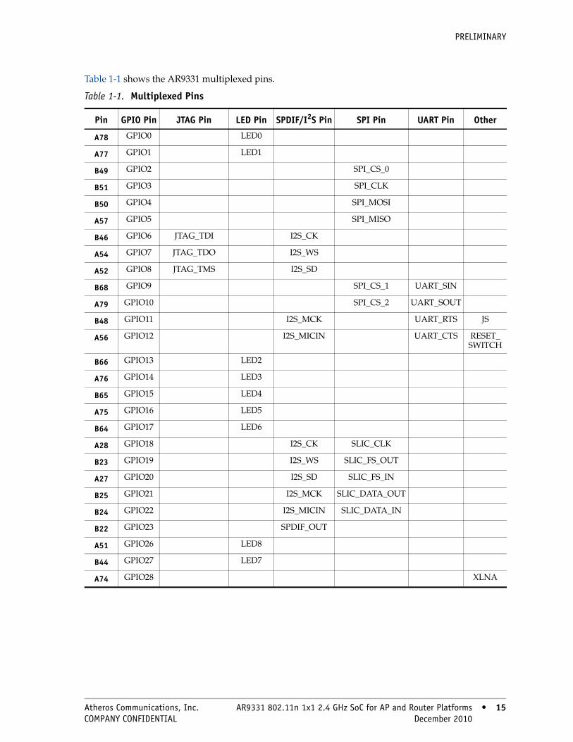
Table 1-1 shows the AR9331 multiplexed pins.
Table 1-1. Multiplexed Pins
Pin GPIO Pin JTAG Pin LED Pin SPDIF/I2S Pin SPI Pin UART Pin Other
A78 GPIO0 LED0
A77 GPIO1 LED1
B49 GPIO2 SPI_CS_0
B51 GPIO3 SPI_CLK
B50 GPIO4 SPI_MOSI
A57 GPIO5 SPI_MISO
B46 GPIO6 JTAG_TDI I2S_CK
A54 GPIO7 JTAG_TDO I2S_WS
A52 GPIO8 JTAG_TMS I2S_SD
B68 GPIO9 SPI_CS_1 UART_SIN
A79 GPIO10 SPI_CS_2 UART_SOUT
B48 GPIO11 I2S_MCK UART_RTS JS
A56 GPIO12 I2S_MICIN UART_CTS RESET_SWITCH
B66 GPIO13 LED2
A76 GPIO14 LED3
B65 GPIO15 LED4
A75 GPIO16 LED5
B64 GPIO17 LED6
A28 GPIO18 I2S_CK SLIC_CLK
B23 GPIO19 I2S_WS SLIC_FS_OUT
A27 GPIO20 I2S_SD SLIC_FS_IN
B25 GPIO21 I2S_MCK SLIC_DATA_OUT
B24 GPIO22 I2S_MICIN SLIC_DATA_IN
B22 GPIO23 SPDIF_OUT
A51 GPIO26 LED8
B44 GPIO27 LED7
A74 GPIO28 XLNA
Atheros Communications, Inc. AR9331 802.11n 1x1 2.4 GHz SoC for AP and Router Platforms • 15 COMPANY CONFIDENTIAL December 2010 • 15

PRELIMINARY
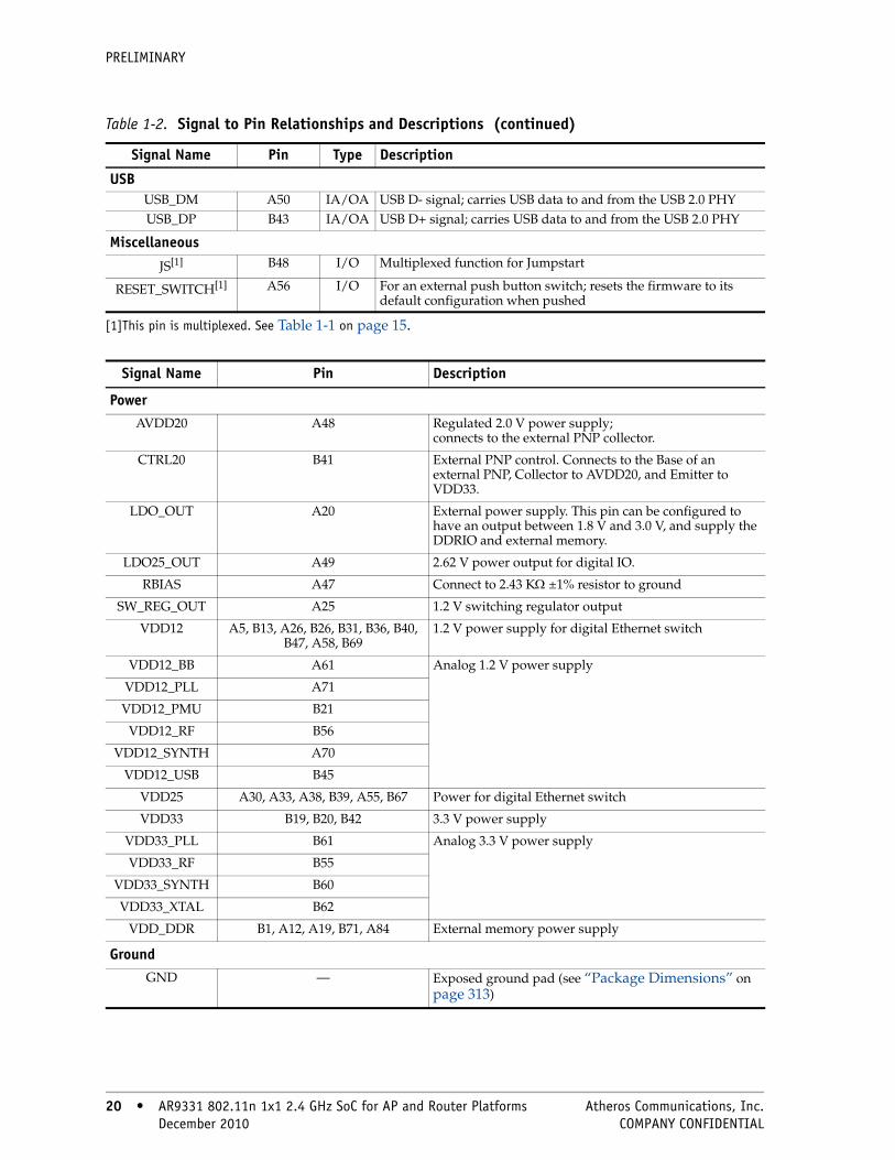
Table 1-2 provides the signal-to-pin relationship information for the AR9331.
Table 1-2. Signal to Pin Relationships and Descriptions
Signal Name Pin Type Description
GeneralRESET_L A72 I External power on reset
XTALI A73 I 40 MHz or 25 MHz crystalXTALO B63 O
RadioRFIN1P A65 IA The first differential RF inputsRFIN1N A64 IARFIN2P A68 IA The second differential RF inputsRFIN2N A69 IARFOUTP A63 OA Differential RF outputsRFOUTN A62 OA
Analog InterfaceBIASREF B59 IA Bias voltage for internal PAXPABIAS B54 OA Bias for optional external power amplifier
External Switch ControlANTA B52 O External RF switch controlANTB A59 OANTC A60 OANTD B53 O
External Memory InterfaceDDR_A_O A4 O 12-bit external memory address busDDR_A_1 B2 ODDR_A_2 A3 O DDR_A_3 B76 ODDR_A_4 A80 ODDR_A_5 B70 ODDR_A_6 A81 ODDR_A_7 A82 ODDR_A_8 B72 ODDR_A_9 A83 ODDR_A_10 B3 ODDR_A_11 B73 ODDR_A_12 B74 ODDR_BA_0 A6 O 2-bit bank address to indicate which bank chip is accessingDDR_BA_1 B4 ODDR_CKE A85 O Deactivates the external memory clock when the signal is highDDR_CK_P B75 O CK_P and CK_N are differential clock inputs. All address and
control signals timing are related to the crossing of the positive edge of CK_P and the negative edge of CK_N.
DDR_CK_N A86 O
DDR_CS_L B5 O External memory chip select signal, active lowDDR_CAS_L B6 O When this signal is asserted, it indicates the address is a column
address. Active when the signal is low.
16 • AR9331 802.11n 1x1 2.4 GHz SoC for AP and Router Platforms Atheros Communications, Inc. 16 • December 2010 COMPANY CONFIDENTIAL

PRELIMINARY
DDR_RAS_L A7 O When this signal is asserted, it indicates the address is a row address. Active when the signal is low.
DDR_DATA_0 B12 I/O 16-bit external memory data busDDR_DATA_1 A13 I/ODDR_DATA_2 B11 I/ODDR_DATA_3 B10 I/ODDR_DATA_4 A11 I/ODDR_DATA_5 B9 I/ODDR_DATA_6 A10 I/ODDR_DATA_7 B8 I/ODDR_DATA_8 B14 I/ODDR_DATA_9 A16 I/ODDR_DATA_10 B15 I/ODDR_DATA_11 A17 I/ODDR_DATA_12 B16 I/ODDR_DATA_13 A18 I/ODDR_DATA_14 B17 I/ODDR_DATA_15 B18 I/ODDR_DQM_0 B7 O DDR data mask for low byte dataDDR_DQM_1 A14 O DDR data mask for high byte dataDDR_DQS_0 A9 I/O DDR data strobe for low byte dataDDR_DQS_1 A15 I/O DDR data strobe for high byte dataDDR_WE_L A8 O When this signal is asserted, it indicates that the following
transaction is write. Active when the signal is low.
Ethernet SwitchTX_P0 A42 OA Ethernet port 0 transmit pairTX_N0 B38 OARX_P0 A41 IA Ethernet port 0 receive pairRX_N0 B37 IATX_P1 B34 OA Ethernet port 1 transmit pairTX_N1 A39 OARX_P1 B35 IA Ethernet port 1 receive pairRX_N1 A40 IATX_P2 A37 OA Ethernet port 2 transmit pairTX_N2 B33 OARX_P2 A36 IA Ethernet port 2 receive pairRX_N2 B32 IATX_P3 B29 OA Ethernet port 3 transmit pairTX_N3 A34 OARX_P3 B30 IA Ethernet port 3 receive pairRX_N3 A35 IATX_P4 A32 OA Ethernet port 4 transmit pairTX_N4 B28 OARX_P4 A31 IA Ethernet port 4 receive pairRX_N4 B27 IA
Table 1-2. Signal to Pin Relationships and Descriptions (continued)
Signal Name Pin Type Description
Atheros Communications, Inc. AR9331 802.11n 1x1 2.4 GHz SoC for AP and Router Platforms • 17 COMPANY CONFIDENTIAL December 2010 • 17

PRELIMINARY
GPIO
GPIO0[1] A78 I/O GPIO multiplexed pin; see Table 1-1
GPIO1[1] A77 I/O
GPIO2[1] B49 I/O
GPIO3[1] B51 I/O
GPIO4[1] B50 I/O
GPIO5[1] A57 I/O
GPIO6[1] B46 I/O
GPIO7[1] A54 I/O
GPIO8[1] A52 I/O
GPIO9[1] B68 I/O
GPIO10[1] A79 I/O
GPIO11[1] B48 I/O
GPIO12[1] A56 I/O
GPIO13[1] B66 I/O
GPIO14[1] A76 I/O
GPIO15[1] B65 I/O
GPIO16[1] A75 I/O
GPIO17[1] B64 I/O
GPIO18[1] A28 I/O
GPIO19[1] B23 I/O
GPIO20[1] A27 I/O
GPIO21[1] B25 I/O
GPIO22[1] B24 I/O
GPIO23[1] B22 I/O
GPIO24 A29 I/O
GPIO26[1] A51 I/O
GPIO27[1] B44 I/O
GPIO28[1] A74 I/O
JTAGJTAG_TCK A53 I JTAG clock
JTAG_TDI[1] B46 I JTAG data input
JTAG_TDO[1] A54 O JTAG data output
JTAG_TMS[1] A52 I JTAG mode select
LED
LED0[1] A78 OD WLAN LED1
LED1[1] A77 OD WLAN LED2
LED2[1] B66 OD Ethernet switch LED1
Table 1-2. Signal to Pin Relationships and Descriptions (continued)
Signal Name Pin Type Description
18 • AR9331 802.11n 1x1 2.4 GHz SoC for AP and Router Platforms Atheros Communications, Inc. 18 • December 2010 COMPANY CONFIDENTIAL

PRELIMINARY
LED3[1] A76 OD Ethernet switch LED2
LED4[1] B65 OD Ethernet switch LED3
LED5[1] A75 OD Ethernet switch LED4
LED6[1] B64 OD Ethernet switch LED5
LED7[1] B44 OD LED
LED8[1] A51 OD LED
I2S/SPDIF
I2S_CK[1] A28, B46 O Stereo clock
I2S_MCK[1] B25, B48 O Master clock
I2S_MICIN[1] A56, B24 I Data input
I2S_SD[1] A27, A52 I/O Serial data input/output
I2S_WS[1] A54, B23 O Word select for stereo0 Left1 Right
SPDIF_OUT[1] B22 O Speaker output
Serial Interface
SPI_CLK[1] B51 O SPI serial interface clock
SPI_CS_0[1] B49 O SPI chip select
SPI_CS_1[1] B68 O
SPI_CS_2[1] A79 O
SPI_MISO[1] A57 O Data transmission from the AR9331 to an external device. On reset, SPI_MOSI (GPIO_4) is input and SPI_MISO (GPIO_5) is output so it can directly interface with a SPI device such as a serial flash. If a serial flash is not used, these pins may be used as GPIO pins.
SPI_MOSI[1] B50 IL Data transmission from an external device to the AR9331. On reset, SPI_MOSI (GPIO_4) is input and SPI_MISO (GPIO_5) is output so it can directly interface with a SPI device such as a serial flash. If a serial flash is not used, these pins may be used as GPIO pins.
SLIC
SLIC_CLK[1] A28 O SLIC clock
SLIC_FS_OUT[1] B23 O Frame sync out
SLIC_FS_IN[1] A27 I Frame sync in
SLIC_DATA_OUT[1] B25 O Data transmitted from the AR9331 to the SLIC
SLIC_DATA_IN[1] B24 I Data transmitted from the SLIC to the AR9331
UART
UART_CTS[1] A56 I UART clear to send signal
UART_RTS[1] B48 O UART ready to send signal (optional UART interface pin)
UART_SIN[1] B68 I Serial data in
UART_SOUT[1] A79 O Serial data out
Table 1-2. Signal to Pin Relationships and Descriptions (continued)
Signal Name Pin Type Description
Atheros Communications, Inc. AR9331 802.11n 1x1 2.4 GHz SoC for AP and Router Platforms • 19 COMPANY CONFIDENTIAL December 2010 • 19
PRELIMINARY
USBUSB_DM A50 IA/OA USB D- signal; carries USB data to and from the USB 2.0 PHYUSB_DP B43 IA/OA USB D+ signal; carries USB data to and from the USB 2.0 PHY
Miscellaneous
JS[1] B48 I/O Multiplexed function for Jumpstart
RESET_SWITCH[1] A56 I/O For an external push button switch; resets the firmware to its default configuration when pushed
[1]This pin is multiplexed. See Table 1-1 on page 15.
Table 1-2. Signal to Pin Relationships and Descriptions (continued)
Signal Name Pin Type Description
Signal Name Pin Description
PowerAVDD20 A48 Regulated 2.0 V power supply;
connects to the external PNP collector.
CTRL20 B41 External PNP control. Connects to the Base of an external PNP, Collector to AVDD20, and Emitter to VDD33.
LDO_OUT A20 External power supply. This pin can be configured to have an output between 1.8 V and 3.0 V, and supply the DDRIO and external memory.
LDO25_OUT A49 2.62 V power output for digital IO.
RBIAS A47 Connect to 2.43 KΩ ±1% resistor to ground
SW_REG_OUT A25 1.2 V switching regulator output
VDD12 A5, B13, A26, B26, B31, B36, B40, B47, A58, B69
1.2 V power supply for digital Ethernet switch
VDD12_BB A61 Analog 1.2 V power supply
VDD12_PLL A71
VDD12_PMU B21
VDD12_RF B56
VDD12_SYNTH A70
VDD12_USB B45
VDD25 A30, A33, A38, B39, A55, B67 Power for digital Ethernet switch
VDD33 B19, B20, B42 3.3 V power supply
VDD33_PLL B61 Analog 3.3 V power supply
VDD33_RF B55
VDD33_SYNTH B60
VDD33_XTAL B62
VDD_DDR B1, A12, A19, B71, A84 External memory power supply
GroundGND — Exposed ground pad (see “Package Dimensions” on
page 313)
20 • AR9331 802.11n 1x1 2.4 GHz SoC for AP and Router Platforms Atheros Communications, Inc. 20 • December 2010 COMPANY CONFIDENTIAL

PRELIMINARY
2. Functional DescriptionFigure 2-1 illustrates the AR9331 functional block diagram.
Table 2-1 summarizes the functional blocks that comprise the AR9331.
Figure 2-1. AR9331 Functional Block Diagram
APB
Clock ResetTimer Interrupt
GPIO
HS-UART
SPI
ROM
OTP
I2S
USB
Ctrl
USBPHY
MultiplexedGPIO
SRAM Async OCPInterface
GMAC0
GMAC1
EthernetSwitch
ETH 5 FE PHY
Bank Arbiters, Wr. Buffer DDR PHYInterface
DDR1/DDR2/SDRAM
R24K
802.11n MAC/BB/Radio
Integrated RFFront End
Integrated CPU,DDR PLLs
Power Management
Multi
plex
edGP
IO
SLIC
Table 2-1. Functional Block Descriptions
Block DescriptionCPU This MIPS 24 K processor can run up to 400 MHz. It includes a 4-way set associative instruction
cache, 4-way set associative data cache, single cycle multiply-accumulate, and MIPS32 and MIPS16 instruction sets. Non-blocking cache reads are also supported.
Memory Controller
The AR9331 has two external memory interfaces. They consist of a 16-bit DDR1/ DDR2 or SDRAM memory interface supporting up to 400 Mbps/pin, and an SPI NOR type flash. The AR9331 also contains internal RAM.
Fast Ethernet Switch
The AR9331 supports four LAN ports and one WAN port with integrated PHY. LED indication for each port is supported. The four LAN ports connect to the CPU through a GMII interface, and four Tx queue priorities are supported in each LAN port. The WAN port can be configured to connect to the CPU using a dedicated MII interface. The MII interface can support up to four priority queues, with either simple priority or a weighted round robin arbitration mechanism. Switch functions such as QoS and VLAN are supported.
GPIO 28 multiplexed GPIO pins can be used as UART, SPI flash interface, JTAG and I2S/SPDIF-out audio interface
I2S/SPDIF ■ I2S/SPDIF out audio interface that support up to 48 KHz sampling clock and a serial clock of more than 512 * sampling frequency. It also supports seamless switching of the audio out stream from I2S to SPDIF. I2S MIC is also supported.
■ Can generate serial clock for various sampling frequencies.
Atheros Communications, Inc. AR9331 802.11n 1x1 2.4 GHz SoC for AP and Router Platforms • 21 COMPANY CONFIDENTIAL December 2010 • 21

PRELIMINARY
2.1 MIPS ProcessorThe AR9331 integrates an embedded MIPS 24Kc processor. For complete information on the 24Kc processor, visit: http://www.mips.com/products/cores/32-bit_cores/MIPS32_24K_Family.php#
Under Processor Cores-24K Family, refer to:■ MIPS32 24Kc Processor Core Datasheet
v3.04 ■ MIPS32 24Kc Processor Core Family
Software User’s Manual v3.05
Under EJTAG, refer to:■ EJTAG Specification v2.60
2.2 ConfigurationTable 2-2 summarizes the configuration settings used by the AR9331. Upon reset, the CPU puts out an address of 0xBFC00000 which is mapped to the flash address space or internal ROM code, using an external pull up/down register to choose if the AR9331 will boot from the Flash or internal ROM.
The AR9331 processor supports a clock frequency of up to 400 MHz.
SLIC A SLIC interface with support for:■ Both master and slave modes■ Configurable number of active slots■ Internal or external frame sync modes■ Supports various frame sync widths; half-bit clock width, one-bit clock width, etc.■ Delayed/non-delayed data modes■ Both internal and external bit clock; the internal clock frequency is programmable■ VOIP applications■ Both Rx and Tx on different (configurable slots)
SPI SPI interface that can be used for serial Flash
USB Universal Serial Bus 2.0 interface supports host/device mode
Wireless MAC/BB/
Radio
Integrated 2.4 GHz 802.11n 1x1 MAC/baseband/radio and RF front end
Table 2-1. Functional Block Descriptions (continued)
Table 2-2. Core Processor Configuration Settings
Setting Description
Cache Size The AR9331 implements a 4-way set associative instruction cache and a four-way set associative data cache. It supports single cycle multiply-accumulate, MIPS32 and MIPS16 instruction sets and non-blocking cached reads.
Endian The AR9331 implements big Endian addressing.
Block Addressing The AR9331 implements sequential ordering.
22 • AR9331 802.11n 1x1 2.4 GHz SoC for AP and Router Platforms Atheros Communications, Inc. 22 • December 2010 COMPANY CONFIDENTIAL

PRELIMINARY
2.3 AR9331 Address MAPThe address space for the AR9331 is divided into three regions. The first region maps to the DDR memory. The second region maps to the APB registers and the third region maps to the AHB registers. Figure 2-2 shows the address space allocation.
2.4 AHB Master BusSome AHB masters are connected to the internal DDR AHB master interface, such as USB, GE0, GE1 WLAN, MAC, etc. The AHB master bus modules each include a DMA to move data, like the descriptors prepared by the CPU, between the AHB masters and the external memory.
2.5 APB BridgeOne 16 MByte window of the AHB address space is devoted to an APB device mapper. The APB space contains the register address spaces of most of the interfaces, including serial flash, GPIO, and UART. This space also provides access to the watchdog timer and four general purpose timers.
2.6 DDR Memory ControllerThe AR9331 supports a 16-bit DDR memory interface of up to 64 MBytes of memory in a single device. It supports one dedicated point-to-point interface for the CPU and similarly
dedicated point-to-point interfaces for the CPU, USB, Ethernet. Write transactions are buffered at each interface. It implements separate arbitration for each bank thus allowing efficient pipelined RAS/CAS/precharge scheduling.
The DDR block has five AHB-slave interfaces for: GE0, GE1, USB, WLAN, and CPU. External DDR is powered by the AR9331 using an external power transistor.
Table 2-3 shows the DDR configurations.
Figure 2-2. Address Space Allocation
Serial Flash
RESERVED
USB AHB Slave
Ethernet 0 AHB Slave
Ethernet 1 AHB Slave
Reserved
APB Address Space (16 MB)
DDR Space (256 MB)
0x1FFF_FFFF0x1EFF_FFFF
0x1BFF_FFFF
0x1AFF_FFFF
0x19FF_FFFF0x18FF_FFFF
0x17FF_FFFF
0x1000_0000
0x0FFF_FFFF
0x0000_0000
MAC_PCU – 1810_8000RTC – 1810_7000Host Interface – 1810_4000DCU – 1810_1000QCU – 1810_0800DMA – 1810_0000MDIO_SLAVE – 180B_8000I2S – 180B_0000MBOX – 180A_0000SLIC – 1809_0000RESERVED – 1808_0000GMAC – 1807_0000RESET – 1806_0000PLL – 1805_0000GPIO – 1804_0000USB – 1803_0000UART – 1802_0000RESERVED – 1801_0000DDR – 1800_0000
Table 2-3. DDR Configurations
Device Type/Total Cap. Device Count Device Type
64 Mbits (4 M x 16) 1 DDR1
128 Mbits (8 M x 16) 1 DDR1
256 Mbits (16 M x 16) 1 DDR1
512 Mbits (32 M x 16) 1 DDR1
256 Mbits (16 M x 16) 1 DDR2
512 Mbits (32 M x 16) 1 DDR2
Atheros Communications, Inc. AR9331 802.11n 1x1 2.4 GHz SoC for AP and Router Platforms • 23 COMPANY CONFIDENTIAL December 2010 • 23
PRELIMINARY
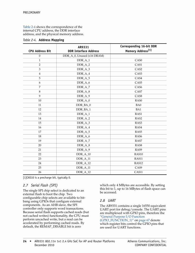
Table 2-4 shows the correspondence of the internal CPU address, the DDR interface address, and the physical memory address.
2.7 Serial Flash (SPI)The single SPI chip select is dedicated to an external flash to boot the chip. Two configurable chip selects are available to bit-bang using GPIOs that configure external components. As an AHB slave, the SPI controller only supports word transactions. Because serial flash supports cached reads (but not cached writes) functionality, the CPU must perform uncached write, but a read can be accelerated by performing cached reads. By default, the REMAP_DISABLE bit is zero
which only 4 MBytes are accessible. By setting this bit to 1, up to 16 MBytes of flash space can be accessed.
2.8 UARTThe AR9331 contains a single 16550 equivalent UART port for debug/console. The UART pins are multiplexed with GPIO pins, therefore the “General Purpose I/O Function (GPIO_FUNCTION_1)” on page 67 denote which register bits control the GPIO pins that are used for UART functions.
Table 2-4. Address Mapping
CPU Address BitAR9331
DDR Interface AddressCorresponding 16-bit DDR
Memory Address[1]
0 DDR_A_0, Unused (x16 DRAM)
1 DDR_A_1 CAS0
2 DDR_A_2 CAS1
3 DDR_A_3 CAS2
4 DDR_A_4 CAS3
5 DDR_A_5 CAS4
6 DDR_A_6 CAS5
7 DDR_A_7 CAS6
8 DDR_A_8 CAS7
9 DDR_A_9 CAS8
10 DDR_A_0 RAS0
11 DDR_BA_0 BA0
12 DDR_BA_1 BA1
13 DDR_A_1 RAS1
14 DDR_A_2 RAS2
15 DDR_A_3 RAS3
16 DDR_A_4 RAS4
17 DDR_A_5 RAS5
18 DDR_A_6 RAS6
19 DDR_A_7 RAS7
20 DDR_A_8 RAS8
21 DDR_A_9 RAS9
22 DDR_A_10 RAS10
23 DDR_A_11 RAS11
24 DDR_A_12 RAS12
25 DDR_A_11 CAS9
26 DDR_A_12 CAS11
[1]CAS10 is a precharge bit, typically 0.
24 • AR9331 802.11n 1x1 2.4 GHz SoC for AP and Router Platforms Atheros Communications, Inc. 24 • December 2010 COMPANY CONFIDENTIAL

PRELIMINARY
2.9 GE0 and GE1The AR9331 integrates two GB Ethernet MACs that are connected to the Ethernet Switch. The GE0 and GE1 support 2 K transmit FIFO and 2 K receive FIFO. The WAN port is a MII interface that connects directly to a PHY inside the Ethernet Switch. Another port connects to the Ethernet Switch using a GMII interface. Through the Ethernet Switch this port connects to the four LAN ports.
The AR9331’s WAN Ethernet PHY (PHY0) can connect directly to the switch as another port, or can be directly to the CPU through an MII interface.
The PHY interfaces (PHY0, PHY1, PHY2, PHY3 and PHY4) can connect to the switch in bridge mode. In this case GE0 must be under reset. All five LAN ports are switched together and connect to the CPU through the GMII interface (MAC0), which is controlled by the ETH_CFG register bit SW_ONLY_MODE. If GE0 connects separately to PHY, then MAC5 should be under reset.
The GMII and MII MAC interface to the Ethernet Switch support four Tx queues, each with its own descriptor chain. A priority of DMA_TX_Q0 is higher than DMA_TX_Q1 and so on. The DMA configuration registers are separate for each queue. Two arbitration mechanisms are supported: one is a simple priority and the other is a weighted round robin arbitration.
Similarly for rest of the queues. In case of Round robin arbitration on a long term the number of packets sent per queue is guaranteed to be in the ratio of the weights programmed. Weight of ZERO is prohibited. It should be noted that the weights are on a packet basis and not on the number of bytes transmitted on that queue. Moreover, a 19-bit free running counter (running on AHB_CLK) value is updated on the descriptor field as shown below on both the transmit and receive descriptor. This update is done as part of the descriptor update that the MAC DMA core already does upon completion of transmit or receive. Software can track the latency on per packet basis using these descriptor Timestamp and the free timer register.
2.10 MDC/MDIO InterfaceThe MDC/MDIO interface, which is internal to the AR9331, allows users to access the internal registers of the Ethernet MAC/PHY. Table 2-5 shows the format required to access the MII registers in the embedded PHY. The PHY-address is 0x00. The OP code 10 indicates the read command and 01 indicates the write command.
The internal switch registers are 32 bits wide, but MDIO access is only 16 bits wide, so two access cycles are required to access all 32 bits of the internal registers.
Address spacing is more than the MDIO-supported 10 bits, thus upper address bits must be written to the internal registers, similar to the page mode access method. For example, register address bits [18:9] are treated as a page address and written out first as High_addr [9:0] (see Table 2-6). Then the register would be accessed via Table 2-5, where Low_addr [7:1] is the register address bit [8:2] and Low_addr [0] is 0 for Data [15:0] or Low_addr [0] is 1 for Data [31:16].
Table 2-5. MDC/MDIO Interface Format
start Op 2’b0 Phy-addr [2.0]
reg_ addr [4:0]
TA [1:0]
Data [15:0]
Table 2-6. Initial Register Address Bits
start Op 2’b11 8’b0 6’b0 High_addr [9:0]
Atheros Communications, Inc. AR9331 802.11n 1x1 2.4 GHz SoC for AP and Router Platforms • 25 COMPANY CONFIDENTIAL December 2010 • 25

PRELIMINARY
2.11 Ethernet Switch ControllerFigure 2-3 shows the Ethernet Switch block diagram.
The Ethernet Switch controller performs the majority of the switch functions of the AR9331. The controller contains five 10/100 Mbps Fast Ethernet ports, each containing four levels of Quality of Service, 802.1Q VLANs, port based VLANs and RMON statistic counters. The AR9331 integrates five 10/100 two speed Ethernet transceivers (PHYs) and one single port 10/100/1000 media access controllers (MAC) as well as a wire-speed, non-blocking shared memory switch fabric.
The included 1 KB entry address lookup table uses two entries per bucket to avoid hash collisions and maintain packet-forwarding performance. The address entry table provides read/write access from the serial and CPU interfaces where each entry can be configured as a static entry. 1024 MAC addresses are supported with automatic learning, aging and static address support. The Ethernet Switch also supports basic switch features including port mirroring, broadcast storm support, flow control in full-duplex, and back pressure in half duplex, 802.3 auto-negotiation, port locking, MIB counters, ingress and egress rate limitation, and automatic speed and duplex communication between PHYs and MACs.
Figure 2-3. Ethernet Switch Block Diagram
26 • AR9331 802.11n 1x1 2.4 GHz SoC for AP and Router Platforms Atheros Communications, Inc. 26 • December 2010 COMPANY CONFIDENTIAL

PRELIMINARY
Table 2-7 summarizes the AR9331 Ethernet Switch functions.
Table 2-7. Ethernet Switch
Block Description
Media Access Controllers
(MAC)
The AR9331 integrates six independent fast Ethernet MACs that perform all functions in the IEEE 802.3 and IEEE 802.3u specifications, including frame formatting, frame stripping, CRC checking, CSMA/CD, collision handling, and back-pressure flow control, etc. Each MAC supports 10 Mbps or 100 Mbps operation in either full-duplex or half-duplex mode.
Full-Duplex Flow Control
The AR9331 device supports IEEE 802.3x full-duplex flow control, force-mode full-duplex flow control, and half-duplex back pressure. If the link partner supports auto-negotiation, the 802.3x full-duplex flow control auto-negotiates between the remote node and the AR9331. If full-duplex flow control is enabled, when free buffer space is almost empty, the AR9331 sends out an IEEE 802.3x compliant PAUSE to stop the remote device from sending more frames.
Half-Duplex Flow Control
Half-duplex flow control regulates the remote station to avoid dropping packets during network congestion. A back pressure function is supported for half-duplex operations. When free buffer space is almost empty, the AR9331 device transmits a jam pattern on the port and forces a collision. If the half-duplex flow control mode is not set, the incoming packet is dropped if no buffer space is available.
Inter-Packet Gap (IPG)
The IPG is the idle time between any to successive packets from the same port. The typical IPG is 9.6 µs for 10 Mbps Ethernet and 960 µs for 100 Mbps Fast Ethernet.
Port Locking The AR9331 supports port locking. If one port is set for port locking, only received frames with the unicast source address found in the ARL table and do not have a member violation, can be sent out. Other blocked frames are dropped or redirected to the CPU port by the control register, LOCK_DROP_EN.
Frame Forwarding Prevention
The AR7240 can be configured to prevent the forwarding of unicast or multicast frames that contain an unknown destination address. This can be accomplished on a per-port basis, so that frames with unknown addresses only go out to the port where a server or router is connected. Broadcast frames forwarded to the CPU port can also be prevented.
Illegal Frames The AR7240 discards all illegal frames such as CRC error, oversized packets (length greater than maximum length), and runt packets (length less than 64 bytes).
VLANs See “VLANs For LAN Ports” on page 28.
QoS See “Quality of Service (QoS) for LAN Ports” on page 29.
Atheros Communications, Inc. AR9331 802.11n 1x1 2.4 GHz SoC for AP and Router Platforms • 27 COMPANY CONFIDENTIAL December 2010 • 27

PRELIMINARY
2.11.1 VLANs For LAN PortsThe switch supports 16 IEEE 802.1Q VLANs and port-based VLAN functionality for all frames, including management frames when 802.1Q is enabled on the ingress port. Untagged frames conform to the port-based VLAN even if the ingress port has 802.1Q mode enabled. See Table 2-8.
Tagging and untagging egress frames is supported using 802.1Q VLANs, or statically using Port Based VLANs. Frames may go out from the switch in three methods:■ Transmit Unmodified
Untagged frames egress a port untagged while tagged frames leave tagged.
■ Transmit Untagged Untagged frames leave a port unmodified while tagged frames leave untagged.
■ Transmit Tagged Tagged frames leave a port unmodified while an IEEE tag is added to untagged frames before leaving.
When a tag is added to an untagged frame, the frame inserts directly after the frame’s source address and includes four bytes.
■ The first byte is always 0x81.■ The second byte is always 0x00.■ PRI bits indicate frame priority determined
by the source port’s priority setting.■ The CFI bit is always set to 0.VID bits indicate the VID assigned to the frame as determined in the source port default VID.
A tagged frame leaving a port tagged may have its VID bits modified. If the ingressing frame’s VID was 0x000, the ingress port’s default VID is assigned to the frame instead.
Double Tagging is a method of isolating one IEEE 802.1Q VLAN from other IEEE 802.1Q VLANs in a hierarchical fashion that is compatible with IEEE 802.1Q ready switches, as long as those switches support a maximum frame size of 1526 bytes or more. In this way, an extra, or double, tag is placed in front of a frame’s normal tag thereby increasing the frame’s size by four bytes.
Ingress double tagging can be selected on a port-by-port basis. Typically, any port that has ingress double tagging enabled will also have egress double tagging enabled. Ingress double tagging enabled ports expect all ingress frames to contain an extra tag that must be removed from the frame before performing the port’s ingress policy on the frame. In this mode, the ingress policy removes the first IEEE 802.3ac tag that appears after the source address in every frame. If the untagged frame is not modified, all data from the removed tags is ignored by the switch.
Table 2-8. Ethernet Switch VLAN
VLAN DescriptionPort-Based Each ingress port contains a register restricting the output (or egress) ports it can send frames
to. This port-based VLAN register has a field called PORT_VID_MEM that contains the port based setting. If bit [0] of PORT_VID_MEM is set to one, the port is allowed to send frames to Port 0, bit [2] for Port 2, and so on. At reset, each port’s PORT_VID_MEM is set to a value of all 1s, except for each port’s own bit, which clears to zero. Note that the CPU port is port 0.
IEEE 802.1Q VLANs
The AR9331 supports a maximum of 16 entries in the VLAN table. The device supports 4096 VLAN ID range from 0 to 4095. The AR9331 only supports shared VLAN learning (SVL). This means that forwarding decisions are based on the frame’s destination MAC address, which should be unique among all VLANs.
28 • AR9331 802.11n 1x1 2.4 GHz SoC for AP and Router Platforms Atheros Communications, Inc. 28 • December 2010 COMPANY CONFIDENTIAL

PRELIMINARY
2.11.2 Quality of Service (QoS) for LAN PortsThe AR9331 recognizes the QoS information of ingress frames and map to different egress priority levels. The AR9331 determines the priority of the frames based on DA, TOS/TC, VLAN, and port. Each has an enable bit that can be applied. When more than one type of priority is selected, the order in which the frame priority should be applied can be determined. Priority enable bits and select order bits are set by port base at 0x110 for port 0, 0x210 for port 1, and so on.
When more than one priority enable bit is set to 1, bits [7:0] in 0x110, 0x210, etc. (DA_PRI_SEL, IP_PRI_SEL, VLAN_PRI_SEL, PORT_PRI_SEL) can determine the order in which the frame priority should be applied. If *_PRI_SEL is set to 00, frame priority is determined by that first. Otherwise, priority is determined by which *_PRI_SEL is set to 01, then 10, 11, etc.
On arrival, packets are directed into one of the four available priority queues based on:
■ Priority bits in the header field■ The frame destination address (if in the
ARL table with a defined priority with the priority bit is enabled)
■ The frame VID (if in the VLAN table and the priority override is enabled)
■ The 802.3 tag containing 802.1p priority information (if enabled on the port)
■ The port’s default priority as defined in the register
Each of the priority classification rules have enables so designers may use any combination; priority can be disabled or the order may be selected separately on a per-port basis.
Congestion in the flow of packets for an extended period of time forces frames to drop without flow control. Higher priority flows receive a higher percentage of the open buffers, and this percentage is determined by the scheduling mode. Features such as back pressure and pause-frame control are implemented to supports zero packet loss during traffic congestion. The AR9331 ensures that all uncongested flows traverse the switch without degradation, regardless od congestion situations elsewhere in the switch.
QoS for the AR9331 may follow one of three priority schemes, either fixed, weighted fair, or a mixed mode scheme. In the fixed priority scheme, all egress packets leave the switch starting with the highest priority queue. Once that queue has been emptied, the next highest priority queue begins its packet dispersal until it has been emptied and so on. This method insures that all high priority packets will be sent out from the switch as soon as possible.
For the weighted fair scheme, packets are egressed from the chip in the order of 8, 4, 2, 1 packets for the four priorities queue of the AR9331. (eight packets egress from the highest priority queue, then four from the second highest queue, and so on). This method allows the highest priority to get its packets out first and the other remaining queues are not totally starved from egressing.
The mixed mode scheme mixes both the weighted fair and fixed schemes. The highest priority queue disperses its packets first until the queue has been emptied, and the remaining queues will follow the 4, 2, 1 weighted egress scheme as mentioned previously. This ensures that the highest priority queue will egress its packets as soon as possible, while the remaining queues equally disperse their packets without queue starvation.
2.12 Rate LimitingThe AR9331 supports port-based ingress and egress rate limiting. All frames may be limited but management frames and known multicast frames are the only types that can be selected by the user. The ingress limit rate may be set from zero to 1 Gbps in steps of 32 Kbps. The port base register is used to determine the limited bytes to count. The default setting for rate limiting is to include the frame’s bytes from the beginning of the preamble to the end of the RCS with a added minimum IFG.
Priority Determined Description
DA Set DA_PRI_EN bit [18] to 1 and add the address to the ARL table-set priority_over_en to 1. ARL priority bits [59:58] can be used as DA priority.
ToS/TC Set IP_PRI_EN bit [16] to 1, and set the IP priority mapping register (0x60–0x6C).
VLAN Set VLAN_PRI_EN (bit [17]) to 1, and set the TAG priority mapping register (0x70).
Port’s Default
Authority
Set PORT_PRI_EN to 1, and set port base register ING_PORT_PRIORITY (bits [19:28] in 0x108, 0x208, etc.).
Atheros Communications, Inc. AR9331 802.11n 1x1 2.4 GHz SoC for AP and Router Platforms • 29 COMPANY CONFIDENTIAL December 2010 • 29

PRELIMINARY
2.13 Broadcast Storm ControlThe AR9331 supports broadcast storm control. Some switch designs may require limiting the reception rate of frames. The types of frames to be limited can be selected separately on a per-port basis.The maximum rate desired needs to be selected by the user and then programmed. Eleven different frame rates from 1k (20K) to 210K per second.
The statistics counter block maintains a set of forty MIB counters per port. These counters provide a set of Ethernet statistics for frames received on ingress and transmitted on egress. A register interface allows the CPU to capture, read, or clear the counter values.
The counters support:
■ RMON MIB■ Ethernet-like MIB■ MIB II■ Bridge MIB■ RFC2819
The CPU interface supports:
■ Autocast MIB counters after half-full■ Autocast MIB counters after time out■ Autocast MIB counters when requested■ Clearing all MIB countersThe MIB counters in the switch are for LAN’s and CPU port. For WAN, the MIB counters are in GE1.
2.14 Switch OperationTwo tables embedded in the AR9331 aid in allocation of ingress packets, the ARL table and the VLAN table.
The address database is stored in the embedded SRAM and can store up to 1024 address entries. The default aging time for this table is 300 seconds. One address can be searched in the table and it may be used to get the next read out of the whole table. Entries in the table may be loaded and purged. All entries maybe be flushed, and this may be divided to flush just non-static entries, all entries per port or all non-static entries per port.
The VLAN table supports a single search, and it may be used to get the next read out of the whole table. Entries may be loaded or purged and entries may be flushed, either as a whole or per port.
2.15 Port MirroringIngress, egress and destination address packets can be mirrored by the AR9331. To mirror the DA packets, the mirror enable bit must be set in the ARL table. To mirror a port, simply set the mirror port number.
Port mirroring is only among the LAN ports and not for WAN.
2.16 Port StatesTable 2-9 shows the port states supported by the AR9331.
Table 2-9. Port States
State Description
Disabled Frames are not allowed to enter or leave a disabled port. Learning does not take place on disabled ports.
Blocking Only MGMP frames are allowed to enter a blocked port. All other frame types are discarded. Learning is disabled on blocked ports.
Listening Only management frames may enter or leave a listening port. All other frame types are discarded. Learning is disabled on listening ports.
Learning Only management frames may enter or leave a learning port. All other frame types are discarded but learning occurs on all good frames, including non-management frames.
Forwarding Normal operation. All frames may enter or leave a forwarding port. Learning occurs on all good frames.
30 • AR9331 802.11n 1x1 2.4 GHz SoC for AP and Router Platforms Atheros Communications, Inc. 30 • December 2010 COMPANY CONFIDENTIAL
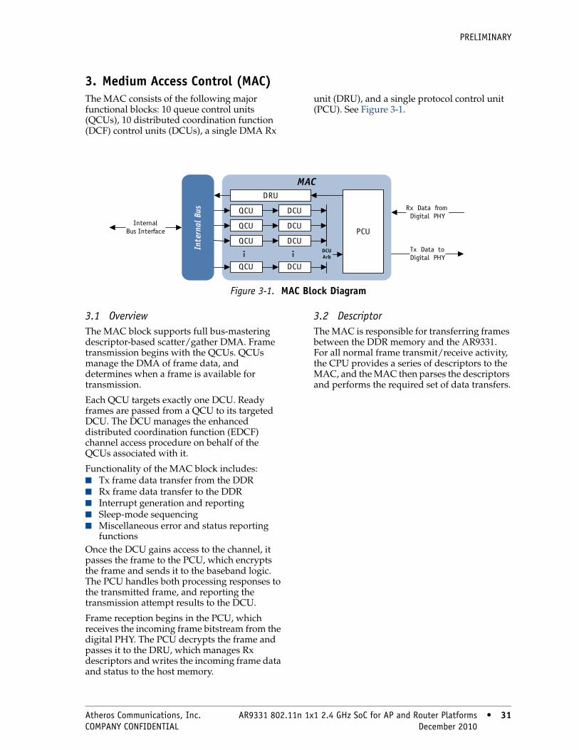
PRELIMINARY
3. Medium Access Control (MAC)The MAC consists of the following major functional blocks: 10 queue control units (QCUs), 10 distributed coordination function (DCF) control units (DCUs), a single DMA Rx
unit (DRU), and a single protocol control unit (PCU). See Figure 3-1.
3.1 OverviewThe MAC block supports full bus-mastering descriptor-based scatter/gather DMA. Frame transmission begins with the QCUs. QCUs manage the DMA of frame data, and determines when a frame is available for transmission.
Each QCU targets exactly one DCU. Ready frames are passed from a QCU to its targeted DCU. The DCU manages the enhanced distributed coordination function (EDCF) channel access procedure on behalf of the QCUs associated with it.
Functionality of the MAC block includes: ■ Tx frame data transfer from the DDR■ Rx frame data transfer to the DDR■ Interrupt generation and reporting■ Sleep-mode sequencing■ Miscellaneous error and status reporting
functionsOnce the DCU gains access to the channel, it passes the frame to the PCU, which encrypts the frame and sends it to the baseband logic. The PCU handles both processing responses to the transmitted frame, and reporting the transmission attempt results to the DCU.
Frame reception begins in the PCU, which receives the incoming frame bitstream from the digital PHY. The PCU decrypts the frame and passes it to the DRU, which manages Rx descriptors and writes the incoming frame data and status to the host memory.
3.2 DescriptorThe MAC is responsible for transferring frames between the DDR memory and the AR9331. For all normal frame transmit/receive activity, the CPU provides a series of descriptors to the MAC, and the MAC then parses the descriptors and performs the required set of data transfers.
Figure 3-1. MAC Block Diagram
Inte
rnal
Bus
Tx Data toDigital PHY
Rx Data fromDigital PHY
MAC
... DCUArb
...
InternalBus Interface
DRU
QCU DCU
PCUQCU DCU
QCU DCU
QCU DCU
Atheros Communications, Inc. AR9331 802.11n 1x1 2.4 GHz SoC for AP and Router Platforms • 31 COMPANY CONFIDENTIAL December 2010 • 31
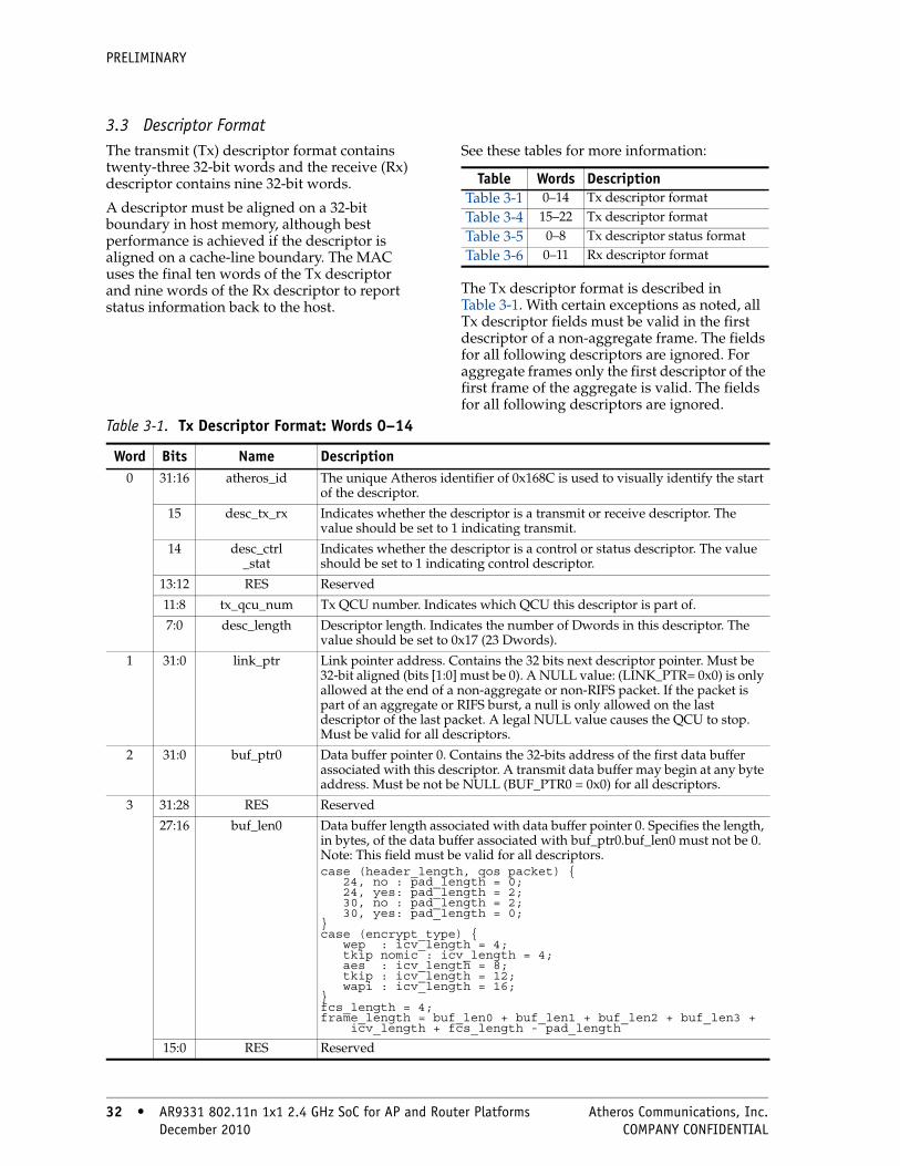
PRELIMINARY
3.3 Descriptor FormatThe transmit (Tx) descriptor format contains twenty-three 32-bit words and the receive (Rx) descriptor contains nine 32-bit words.
A descriptor must be aligned on a 32-bit boundary in host memory, although best performance is achieved if the descriptor is aligned on a cache-line boundary. The MAC uses the final ten words of the Tx descriptor and nine words of the Rx descriptor to report status information back to the host.
See these tables for more information:
The Tx descriptor format is described in Table 3-1. With certain exceptions as noted, all Tx descriptor fields must be valid in the first descriptor of a non-aggregate frame. The fields for all following descriptors are ignored. For aggregate frames only the first descriptor of the first frame of the aggregate is valid. The fields for all following descriptors are ignored.
Table Words DescriptionTable 3-1 0–14 Tx descriptor format
Table 3-4 15–22 Tx descriptor format
Table 3-5 0–8 Tx descriptor status format
Table 3-6 0–11 Rx descriptor format
Table 3-1. Tx Descriptor Format: Words 0–14
Word Bits Name Description0 31:16 atheros_id The unique Atheros identifier of 0x168C is used to visually identify the start
of the descriptor.
15 desc_tx_rx Indicates whether the descriptor is a transmit or receive descriptor. The value should be set to 1 indicating transmit.
14 desc_ctrl_stat
Indicates whether the descriptor is a control or status descriptor. The value should be set to 1 indicating control descriptor.
13:12 RES Reserved
11:8 tx_qcu_num Tx QCU number. Indicates which QCU this descriptor is part of.
7:0 desc_length Descriptor length. Indicates the number of Dwords in this descriptor. The value should be set to 0x17 (23 Dwords).
1 31:0 link_ptr Link pointer address. Contains the 32 bits next descriptor pointer. Must be 32-bit aligned (bits [1:0] must be 0). A NULL value: (LINK_PTR= 0x0) is only allowed at the end of a non-aggregate or non-RIFS packet. If the packet is part of an aggregate or RIFS burst, a null is only allowed on the last descriptor of the last packet. A legal NULL value causes the QCU to stop. Must be valid for all descriptors.
2 31:0 buf_ptr0 Data buffer pointer 0. Contains the 32-bits address of the first data buffer associated with this descriptor. A transmit data buffer may begin at any byte address. Must be not be NULL (BUF_PTR0 = 0x0) for all descriptors.
3 31:28 RES Reserved
27:16 buf_len0 Data buffer length associated with data buffer pointer 0. Specifies the length, in bytes, of the data buffer associated with buf_ptr0.buf_len0 must not be 0. Note: This field must be valid for all descriptors.case (header_length, qos packet) { 24, no : pad_length = 0; 24, yes: pad_length = 2; 30, no : pad_length = 2; 30, yes: pad_length = 0;}case (encrypt_type) { wep : icv_length = 4; tkip nomic : icv_length = 4; aes : icv_length = 8; tkip : icv_length = 12; wapi : icv_length = 16;}fcs_length = 4;frame_length = buf_len0 + buf_len1 + buf_len2 + buf_len3 + icv_length + fcs_length - pad_length
15:0 RES Reserved
32 • AR9331 802.11n 1x1 2.4 GHz SoC for AP and Router Platforms Atheros Communications, Inc. 32 • December 2010 COMPANY CONFIDENTIAL

PRELIMINARY
4 31:0 buf_ptr1 Data buffer pointer 1. Contains the 32-bits address of the second data buffer associated with this descriptor. A transmit data buffer may begin at any byte address. Only valid if BUF_PTR0 is not NULL.
5 31:28 RES Reserved
27:16 buf_len1 Data buffer length associated with data buffer pointer 1. BUF_LEN1 can only be 0 if and only if BUF_PTR1 is NULL. See BUF_LEN0 for details.
15:0 RES Reserved
6 31:0 buf_ptr2 Data buffer pointer 2. Contains the 32-bits address of the third data buffer associated with this descriptor. A transmit data buffer may begin at any byte address. Only valid if BUF_PTR0 and BUF_PTR1 are not NULL.
7 31:28 RES Reserved
27:16 buf_len2 Data buffer length associated with data buffer pointer 2. BUF_LEN2 can only be 0 if and only if BUF_PTR2 is NULL. See BUF_LEN0 for details.
15:0 RES Reserved
8 31:0 buf_ptr3 Data buffer pointer 3. Contains the 32-bits address of the third data buffer associated with this descriptor. A transmit data buffer may begin at any byte address. Only valid if BUF_PTR0, BUF_PTR1, and BUF_PTR2 are not NULL.
9 31:28 RES Reserved
27:16 buf_len3 Data buffer length associated with data buffer pointer 2. BUF_LEN2 can only be 0 if and only if BUF_PTR3 is NULL. See BUF_LEN0 for details.
15:0 RES Reserved
10 31:16 tx_desc_id Tx descriptor sequence number. Software will select a unique sequence number associated with this descriptor. This value is copied to the TX_DESC_ID in the transmit status.
15:0 ptr_checksum Memory pointer checksum. Verifies the integrity of the memory pointers/addresses in this descriptor. The equation looks like this:checksum[31:0] = TXC[0]+TXC[1]+TXC[2]+TXC[3]+TXC[4]+ TXC[5]+TXC[6]+TXC[7]+TXC[8]+TXC[9];ptr_checksum[15:0] = checksum[31:16] + checksum[15:0];
The carry bits above the MSB of the checksum or PTR_CHECKSUM will disappear.
Table 3-1. Tx Descriptor Format: Words 0–14
Word Bits Name Description
Atheros Communications, Inc. AR9331 802.11n 1x1 2.4 GHz SoC for AP and Router Platforms • 33 COMPANY CONFIDENTIAL December 2010 • 33

PRELIMINARY
11 31 cts_enable Self-CTS enable. Precedes the frame with CTS flag. If set, the PCU first sends a CTS before sending the frame described by the descriptor; used mainly for 802.11g frames to quiet legacy stations before sending a frame the legacy stations cannot interpret, even at the PHY level. At most only one of the RTS_ENABLE and CTS_ENABLE bits may be set; it is illegal to set both.
30 dest_index_valid
Destination index valid flag. Specifies whether the contents of the DestIdx field are valid.
29 int_req Interrupt request flag. Set to one by the driver to request that the DMA engine generate an interrupt upon completion of the frame to which this descriptor belongs. Note: This field must be valid and identical for all descriptors of the frame. That is, all descriptors for the frame must have this flag set, or all descriptors for the frame must have this flag clear.
28:25 res Reserved
24 clear_dest_mask
Clear destination mask bit flag. If set, instructs the DCU to clear the destination mask bit at the index specified by the dest_index field.
23 veol Virtual end-of-list flag. When set, indicates that the QCU should act (mostly) as if this descriptor had a NULL LINK_PTR, even though its LINK_PTR field may be non-NULL. Note: This field must be valid in the final descriptor of a frame and must be clear for all other descriptors of the frame.
22 rts_enable RTS enable. If set, the PCU transmits the frame using the RTS/CTS protocol. If clear, the PCU transmits the frame without transmitting a RTS. At most only one of the RTS_ENABLE and CTS_ENABLE bits may be set; it is illegal to set both.
21:16 tpc_0 TPC for Tx series 0. These bits pass unchanged to the baseband, where they control Tx power for the frame.
15 clear_retry Setting this bit disables the retry bit from being set in the Tx header on a frame retry; applies to both aggregate and non-aggregate frames.
14 low_rx_chain When set to 1, indicates that switches the Rx chain mask to low power mode after transmitted this frame.
13 fast_ant_mode
Fast antenna mode. If set to 0, this means that this Tx frame to use the omni antenna mechanism. if set to 1, then the opposite omni antenna should be used.
12 vmf Virtual more fragment. If this bit is set, bursting is enabled for this frame. If there is no burst in progress, it will initiate a CTS protected burst if CTS_ENABLE is set. If there is a previous burst in progress, it ignores the CTS_ENABLE bit as assume that this burst is protected.
11:0 frame_length Frame length. Specifies the length, in bytes, of the entire MAC frame, including the FCS, IC, and ICV fields.
Table 3-1. Tx Descriptor Format: Words 0–14
Word Bits Name Description
34 • AR9331 802.11n 1x1 2.4 GHz SoC for AP and Router Platforms Atheros Communications, Inc. 34 • December 2010 COMPANY CONFIDENTIAL

PRELIMINARY
12 31 more_rifs More RIFS burst flag; When set, indicates that the current packet is not the last packet of an aggregate. All descriptors for all packets of a RIFS burst except the descriptors of the last packet must have this bit set. All descriptors of the last packet of a RIFS burst must have this bit clear.
30 is_agg This packet is part of an aggregate flag. All descriptors of the all packets in an aggregate must have this bit set.
29 more_agg More aggregate flag; When set, indicates that the current packet is not the last packet of an aggregate. All descriptors for all packets of an aggregate except the descriptors of the last packet must have this bit set. All descriptors of the last packet of an aggregate must have this bit clear.
28 ext_and_ctl Extension and control channel enable. Only four combinations are allowed; otherwise DESC_CONFIG_ERROR asserts. When neither EXT_ONLY nor EXT_AND_CTL are set, the RTS/CTS and data frame is sent based on the bandwidth: HT20 when 20_40 is set to 0 and HT40 shared when 20_40 is set to 1 (RTS/CTS frames are sent at in HT40 duplicate mode if 20_40 is set to 1). When EXT_AND_CTL is set the RTS/CTS and data frame is sent at HT40 duplicate. When EXT_ONLY is set the RTS/CTS and data frame is sent out in HT20 extension channel mode.
ETX_AND_CTL 20_40 DATA RTS/CTS
0 0 HT20 Control HT20 Control
0 1 HT40 Shared HT40 Duplicate
1 1 HT40 Duplicate HT40 Duplicate
27 RES Reserved
26 corrupt_fcs Corrupt packet FCS; When set, the FCS of the packet will be inverted to guarantee the transmitted FCS is incorrect.
25 RES Reserved
24 no_ack No ACK flag; When set, indicates to the PCU that it should not expect to receive (and should not wait for) an ACK for the frame. Must be set for any frame that has the 802.11 NoACK bit set in the QoS field. Also must be set for all other frame types (such as beacons and other broadcast/multicast frames) that do not receive ACKs.
23:20 frame_type Frame type indication; indicates what type of frame is being sent:
15:5 Reserved
4 Probe response
3 Beacon
2 PS-Poll
1 ATIM
0 Frame type, other than the types listed in [15:1]
19:13 dest_index Destination table index. Specifies an index into an on-chip table of per-destination information. The PCU fetches the encryption key from the specified index in this table and uses this key to encrypt the frame. The DMA logic uses the index to maintain per-destination transmit filtering status and other related information.
12 more More descriptors in this frame flag. Set to one by the driver to indicate that there are additional descriptors (that is, DMA fragments) in the current frame. The last descriptor of a packet must have this bit set to 0. Note: This field must be valid for all descriptors.
11:9 pa Pre-distortion chain mask
8:0 RES Reserved
Table 3-1. Tx Descriptor Format: Words 0–14
Word Bits Name Description
Atheros Communications, Inc. AR9331 802.11n 1x1 2.4 GHz SoC for AP and Router Platforms • 35 COMPANY CONFIDENTIAL December 2010 • 35
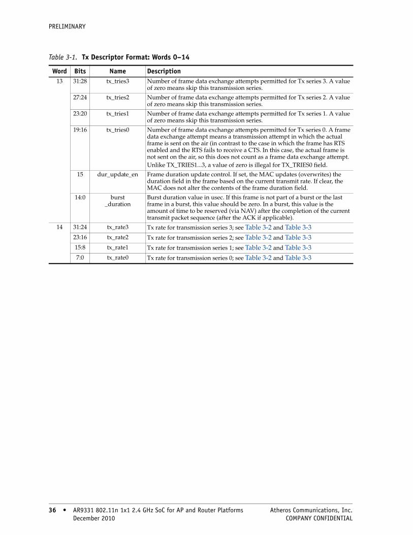
PRELIMINARY
13 31:28 tx_tries3 Number of frame data exchange attempts permitted for Tx series 3. A value of zero means skip this transmission series.
27:24 tx_tries2 Number of frame data exchange attempts permitted for Tx series 2. A value of zero means skip this transmission series.
23:20 tx_tries1 Number of frame data exchange attempts permitted for Tx series 1. A value of zero means skip this transmission series.
19:16 tx_tries0 Number of frame data exchange attempts permitted for Tx series 0. A frame data exchange attempt means a transmission attempt in which the actual frame is sent on the air (in contrast to the case in which the frame has RTS enabled and the RTS fails to receive a CTS. In this case, the actual frame is not sent on the air, so this does not count as a frame data exchange attempt. Unlike TX_TRIES1...3, a value of zero is illegal for TX_TRIES0 field.
15 dur_update_en Frame duration update control. If set, the MAC updates (overwrites) the duration field in the frame based on the current transmit rate. If clear, the MAC does not alter the contents of the frame duration field.
14:0 burst_duration
Burst duration value in usec. If this frame is not part of a burst or the last frame in a burst, this value should be zero. In a burst, this value is the amount of time to be reserved (via NAV) after the completion of the current transmit packet sequence (after the ACK if applicable).
14 31:24 tx_rate3 Tx rate for transmission series 3; see Table 3-2 and Table 3-323:16 tx_rate2 Tx rate for transmission series 2; see Table 3-2 and Table 3-315:8 tx_rate1 Tx rate for transmission series 1; see Table 3-2 and Table 3-37:0 tx_rate0 Tx rate for transmission series 0; see Table 3-2 and Table 3-3
Table 3-1. Tx Descriptor Format: Words 0–14
Word Bits Name Description
36 • AR9331 802.11n 1x1 2.4 GHz SoC for AP and Router Platforms Atheros Communications, Inc. 36 • December 2010 COMPANY CONFIDENTIAL

PRELIMINARY
Table 3-2. MAC Rate Encodings
MAC Rate Encoding Protocol
0x01 Reserved
0x02
0x03
0x06
0x07
0x8 OFDM_48Mb
0x9 OFDM_24Mb
0xA OFDM_12Mb
0xB OFDM_6Mb
0xC OFDM_54Mb
0xD OFDM_36Mb
0xE OFDM_18Mb
0xF OFDM_9Mb
0x18 CCK_11Mb_L
0x19 CCK_5_5Mb_L
0x1A CCK_2Mb_L
0x1B CCK_1Mb_L
0x1C CCK_11Mb_S
0x1D CCK_5_5Mb_S
0x1E CCK_2Mb_S
Table 3-3. Tx Rates[1]
Rate Desc StreamHT20;
GI= 0 MbpsHT20;
GI = 1 MbpsHT40;
GI= 0 MbpsHT40;
GI= 1 Mbps
0x80 MCS 0 1 6.5 7.2 13.5 15
0x81 MCS 1 1 13 14.4 27 30
0x82 MCS 2 1 19.5 21.7 40.5 45
0x83 MCS 3 1 26 28.9 54 60
0x84 MCS 4 1 39 43.3 81 90
0x85 MCS 5 1 52 57.8 108 120
0x86 MCS 6 1 58.5 65.0 121.5 135
0x87 MCS 7 1 65 72.2 135 150
[1]All rates not listed are reserved. Note that for short guard interval (GI=1), HT20 mode is allowed.
Atheros Communications, Inc. AR9331 802.11n 1x1 2.4 GHz SoC for AP and Router Platforms • 37 COMPANY CONFIDENTIAL December 2010 • 37

PRELIMINARY
The Tx descriptor format for words 15 through 22 is described in Table 3-4.
Table 3-4. DMA Tx Descriptor Format for Words 15–22
Word Bits Name Description15 31 rts_cts
_qual1Qualifies RTS_ENABLE or CTS_ENABLE in the Tx descriptor for Tx series 1
1 Default behavior with respect to RTS_ENABLE and CTS_ENABLE
30:16 packet_duration1
Packet duration 1 (in μs); Duration of the actual Tx frame associated with TXRate1. This time does not include RTS, CTS, ACK, or any associated SIFS.
15 rts_cts_qual0
Qualifies RTS_ENABLE or CTS_ENABLE in the Tx descriptor for Tx series 0
1 Default behavior with respect to RTS_ENABLE and CTS_ENABLE
14:0 packet_duration0
Packet duration 0 (in μs); Duration of the actual Tx frame associated with TXRate0. This time does not include RTS, CTS, ACK, or any associated SIFS.
16 31 rts_cts_qual3
Qualifies RTS_ENABLE or CTS_ENABLE in the Tx descriptor for Tx series 3
1 Default behavior with respect to RTS_ENABLE and CTS_ENABLE
30:16 packet_duration3
Packet duration 3 (in μs); Duration of the actual Tx frame associated with TXRate3. This time does not include RTS, CTS, ACK, or any associated SIFS.
15 rts_cts_qual2
Qualifies RTS_ENABLE or CTS_ENABLE in the Tx descriptor for Tx series 2
1 Default behavior with respect to RTS_ENABLE and CTS_ENABLE
14:0 packet_duration2
Packet duration 2 (in μs); Duration of the actual Tx frame associated with TXRate2. This time does not include RTS, CTS, ACK, or any associated SIFS.
17 31:30 RES Reserved
29 dc_ap_sta_sel
Select for remaining the TBTT between TSF and TSF2, where 0 is from TSF and 1 is from TSF2. Should be used only when both AP_STA_ENABLE and TXOP_TBTT_LIMIT_ENABLE are enabled.
28:26 encrypt_type Encryption type; DMA engine must the number of necessary extra Dwords at the end of a packet to account for the encryption ICV which is generated by hardware. The encrypt type fields must be valid for all descriptors.
0 None; 0 pad bytes
1 WEP or TKIP (no MIC); 4 pad bytes
2 AES; 8 pad bytes
3 TKIP; 12 pad bytes
4 WAPI; 16 pad bytes
7:5 Reserved
25:18 pad_delim Pad delimiters; Between each packet of an A-MPDU aggregate the hardware will insert a start delimiter which includes the length of the next frame. Sometimes hardware on the transmitter or receiver requires some extra time between packets which can be satisfied by inserting zero length delimiters. This field indicates the number of extra zero length delimiters to add.
17:16 RES Reserved
15:0 agg_length Aggregate (A-MPDU) length; the aggregate length is the number of bytes of the entire aggregate. This length should be computed as:delimiters = start_delim + pad_delim;frame_pad = (frame_length % 4) ? (4 - (frame_length % 4)) : 0agg_length = sum_of_all (frame_length + frame_pad + 4 * delimiters)
For the last packet of an aggregate the FRAME_PAD = 0 and delimiter= 0, frame_pad aligns to the next delimiter to be Dword aligned. Each delimiter is 4 bytes long. PAD_DELIM is the number of zero-length delimiters used to introduce an extra time gap between packets. START_DELIM is always 1 and includes the length of the next packet in the aggregate.
38 • AR9331 802.11n 1x1 2.4 GHz SoC for AP and Router Platforms Atheros Communications, Inc. 38 • December 2010 COMPANY CONFIDENTIAL
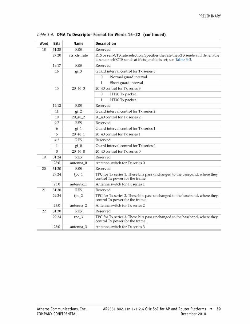
PRELIMINARY
18 31:28 RES Reserved
27:20 rts_cts_rate RTS or self-CTS rate selection. Specifies the rate the RTS sends at if rts_enable is set, or self CTS sends at if cts_enable is set; see Table 3-3.
19:17 RES Reserved
16 gi_3 Guard interval control for Tx series 3
0 Normal guard interval
1 Short guard interval
15 20_40_3 20_40 control for Tx series 3
0 HT20 Tx packet
1 HT40 Tx packet
14:12 RES Reserved
11 gi_2 Guard interval control for Tx series 2
10 20_40_2 20_40 control for Tx series 2
9:7 RES Reserved
6 gi_1 Guard interval control for Tx series 1
5 20_40_1 20_40 control for Tx series 1
4:2 RES Reserved
1 gi_0 Guard interval control for Tx series 0
0 20_40_0 20_40 control for Tx series 0
19 31:24 RES Reserved
23:0 antenna_0 Antenna switch for Tx series 0
20 31:30 RES Reserved
29:24 tpc_1 TPC for Tx series 1. These bits pass unchanged to the baseband, where they control Tx power for the frame.
23:0 antenna_1 Antenna switch for Tx series 1
21 31:30 RES Reserved
29:24 tpc_2 TPC for Tx series 2. These bits pass unchanged to the baseband, where they control Tx power for the frame.
23:0 antenna_2 Antenna switch for Tx series 2
22 31:30 RES Reserved
29:24 tpc_3 TPC for Tx series 3. These bits pass unchanged to the baseband, where they control Tx power for the frame.
23:0 antenna_3 Antenna switch for Tx series 3
Table 3-4. DMA Tx Descriptor Format for Words 15–22 (continued)
Word Bits Name Description
Atheros Communications, Inc. AR9331 802.11n 1x1 2.4 GHz SoC for AP and Router Platforms • 39 COMPANY CONFIDENTIAL December 2010 • 39
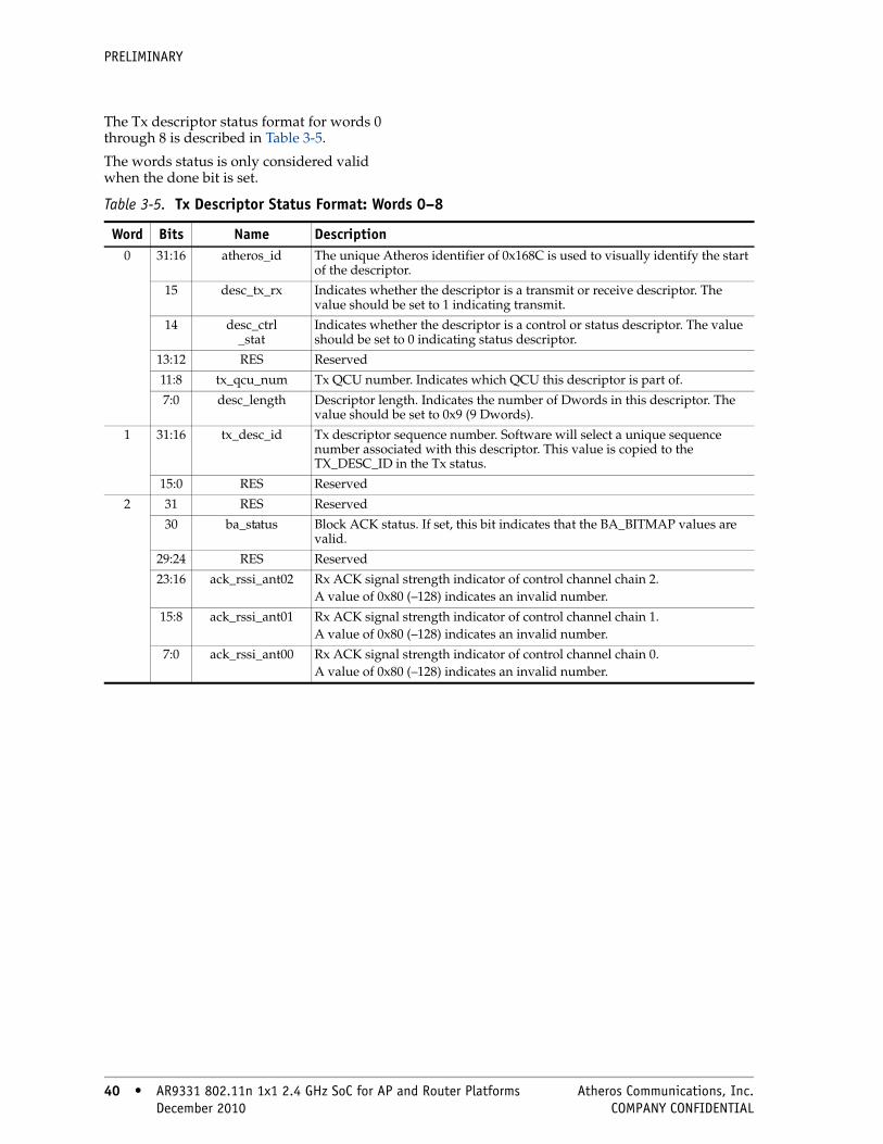
PRELIMINARY
The Tx descriptor status format for words 0 through 8 is described in Table 3-5.
The words status is only considered valid when the done bit is set.
Table 3-5. Tx Descriptor Status Format: Words 0–8
Word Bits Name Description0 31:16 atheros_id The unique Atheros identifier of 0x168C is used to visually identify the start
of the descriptor.
15 desc_tx_rx Indicates whether the descriptor is a transmit or receive descriptor. The value should be set to 1 indicating transmit.
14 desc_ctrl_stat
Indicates whether the descriptor is a control or status descriptor. The value should be set to 0 indicating status descriptor.
13:12 RES Reserved
11:8 tx_qcu_num Tx QCU number. Indicates which QCU this descriptor is part of.
7:0 desc_length Descriptor length. Indicates the number of Dwords in this descriptor. The value should be set to 0x9 (9 Dwords).
1 31:16 tx_desc_id Tx descriptor sequence number. Software will select a unique sequence number associated with this descriptor. This value is copied to the TX_DESC_ID in the Tx status.
15:0 RES Reserved
2 31 RES Reserved
30 ba_status Block ACK status. If set, this bit indicates that the BA_BITMAP values are valid.
29:24 RES Reserved
23:16 ack_rssi_ant02 Rx ACK signal strength indicator of control channel chain 2.A value of 0x80 (–128) indicates an invalid number.
15:8 ack_rssi_ant01 Rx ACK signal strength indicator of control channel chain 1.A value of 0x80 (–128) indicates an invalid number.
7:0 ack_rssi_ant00 Rx ACK signal strength indicator of control channel chain 0.A value of 0x80 (–128) indicates an invalid number.
40 • AR9331 802.11n 1x1 2.4 GHz SoC for AP and Router Platforms Atheros Communications, Inc. 40 • December 2010 COMPANY CONFIDENTIAL

PRELIMINARY
3 31:20 RES Reserved
19 tx_timer_expired
Tx timer expired. This bit is set when the Tx frame is taking longer to send to the baseband than is allowed based on the TX_TIMER register. Some regulatory domains require that Tx packets may not exceed a certain amount of transmit time.
18 RES Reserved
17 tx_data_underrun_err
Tx data underrun error. These error conditions occur on aggregate frames when the underrun condition happens while the MAC is sending the data portion of the frame or delimiters.
16 tx_delmtr_underrun_err
Tx delimiter underrun error. These error conditions occur on aggregate frames when the underrun conditions happens while the MAC is sending delimiters.
15:12 virtual_retry_cnt Virtual collision count. Reports the number of virtual collisions that occurred before transmission of the frame ended. The counter value saturates at 0xF. A virtual collision refers to the case, as described in the 802.11e QoS specification, in which two or more output queues are contending for a TXOP simultaneously. In such cases, all lower-priority output queues experience a virtual collision in which the frame is treated as if it had been sent on the air but failed to receive an ACK.
11:8 data_fail_cnt Data failure count. Reports the number of times the actual frame (as opposed to the RTS) was sent but no ACK was received for the final transmission series (see the FINAL_TS_INDEX field).
7:4 rts_fail_cnt RTS failure count. Reports the number of times an RTS was sent but no CTS was received for the final transmission series (see the FINAL_TX_INDEX field). For frames that have the RTS_ENABLE bit clear, this count always will be zero. Note that this count is incremented only when the RTS/CTS exchange fails. In particular, this count is not incremented if the RTS/CTS exchange succeeds but the frame itself fails because no ACK was received.
3 filtered Frame transmission filter indication. If set, indicates that the frame was not transmitted because the corresponding destination mask bit was set when the frame reached the PCU or if the frame violated TXOP on the first packet of a burst. Valid only if FRM_XMIT_OK is clear.
2 fifo_underrun Tx FIFO underrun flag. If set, transmission of the frame failed because the DMA engine was not able to supply the PCU with data as quickly as the baseband was requesting transmit data. Only valid for non-aggregate or non-RIFS underrun conditions unless the underrun occurred on the first packet of the aggregate or RIFS burst. See also the description for TX_DELMTR_UNDERRUN_ERR and TX_DATA_UNDERRUN_ERR. Valid only if FRM_XMIT_OK is clear.
1 excessive_retries
Excessive tries flag. If set, transmission of the frame failed because the try limit was reached before the frame transmitted. Valid only if FRM_XMIT_OK is clear.
0 frm_xmit_ok Frame transmission success flag. If set, the frame was transmitted successfully. If clear, no ACK or BA was received successfully.
4 31:0 send_timestamp
Timestamp at start of transmit. A snapshot of the lower 32 bits of the PCU timestamp (TSF value). This field can be used to aid the software driver in implementing requirements associated with the aMaxTransmitMSDULifetime MAC attribute. The transmit timestamp is sampled on the rising of tx_frame signal which goes from the MAC to the baseband. This value corresponds to the last attempt at packet transmission not the first attempt.For support location mode, this value refers to the fast timestamp value, and is valid when word 8, bit [27] of the Tx Descriptor Status is high.
Table 3-5. Tx Descriptor Status Format: Words 0–8
Word Bits Name Description
Atheros Communications, Inc. AR9331 802.11n 1x1 2.4 GHz SoC for AP and Router Platforms • 41 COMPANY CONFIDENTIAL December 2010 • 41

PRELIMINARY
5 31:0 ba_bitmap_0-31 Block ACK bitmap 0 to 31. These bits are the values from the block ACK received after the successful transmission of an aggregate frame. If set, bit [0] represents the successful reception of the packet with the sequence number matching the seq_num value.
6 31:0 ba_bitmap_32-63 Block ACK bitmap 32 to 63. These bits are the values from the block ACK received after the successful transmission of an aggregate frame. If set, bit [32] represents the successful reception of the packet with the sequence number matching the seq_num value + 32.
7 31:24 ack_rssi_combined
Rx ACK signal strength indicator of combination of all active chains on the control and extension channels. The value of 0x80 (–128) is used to indicate an invalid number.
23:16 ack_rssi_ant12 Rx ACK signal strength indicator of control channel chain 2.A value of 0x80 (–128) indicates an invalid number.
15:8 ack_rssi_ant11 Rx ACK signal strength indicator of control channel chain 1.A value of 0x80 (–128) indicates an invalid number.
7:0 ack_rssi_ant10 Rx ACK signal strength indicator of control channel chain 0.A value of 0x80 (–128) indicates an invalid number.
8 31:28 tid Traffic Identifier (TID) of block ACK. Indicates the TID of the response block ACK. This field is only valid on the last descriptor of the last packet of an aggregate.
27 tx_location_mode The location mode indicator of the Tx Descriptor Status. This field indicates that the send_timestamp field (word 8, bit [31:0]) is used for the location mode, and not as the TSF value for the PCU timestamp.
26 RES Reserved
25 pwr_mgmt Power management state. Indicates the value of the PwrMgt bit in the frame control field of the response ACK frame.
24:23 RES Reserved
22:21 final_tx_index Final transmission attempt series index. Specifies the number of the Tx series that caused frame transmission to terminate.
20 RES Reserved
8 (Cont.)
19:18 RES Reserved
17 txop_exceeded TXOP has been exceeded. Indicates that this transmit frame had to be filtered because the amount of time to transmit this packet sequence would exceeded the TXOP limit. This should only occur when software programs the TXOP limit improperly.
16:13 RES Reserved
12:1 seq_num The starting sequence number is the value of the Block ACK Starting Sequence Control field in the response Block ACK. Only consulted if the Tx frame was an aggregate.
0 done Descriptor completion flag. Set to one by the DMA engine when it has finished processing the descriptor and has updated the status information. Valid only for the final descriptor of a non-aggregate frame, regardless of the state of the FrTxOK flag. For an aggregate frame it is valid for only the final descriptor of the final packet of an aggregate. The driver is responsible for tracking what descriptors are associated with a frame. When the DMA engine sets the DONE flag in the final descriptor of a frame, the driver must be able to determine what other descriptors belong to the same frame and thus also have been consumed.
Table 3-5. Tx Descriptor Status Format: Words 0–8
Word Bits Name Description
42 • AR9331 802.11n 1x1 2.4 GHz SoC for AP and Router Platforms Atheros Communications, Inc. 42 • December 2010 COMPANY CONFIDENTIAL

PRELIMINARY
The DMA Rx logic (the DRU block) manages Rx descriptors and transfers the incoming frame data and status to the host through the AHB bus.
Words 0, and 2 are valid for all descriptors. Words 0, 2, and 11 is valid for the last
descriptor of each packets. Words 0–11 are valid for the last descriptor of an aggregate or last descriptor of a stand-alone packet. Additional validity qualifiers are described individually. See Table 3-6.
Table 3-6. DMA Rx Descriptor Format for Words 0–11
Word Bits Name Description0 31:16 atheros_id The unique Atheros identifier of 0x168C is used to visually identify the start
of the descriptor.
15 desc_tx_rx Indicates whether the descriptor is a Tx or Rx descriptor. The value should be set to 1 indicating transmit.
14 desc_ctrl_stat
Indicates whether the descriptor is a control or status descriptor. The value should be set to 1 indicating status descriptor.
13:9 RES Reserved
8 rx_priority 0 Low priority queue
1 High priority queue
7:0 desc_length Descriptor length. Indicates the number of Dwords in this descriptor. The value should be set to 0x9 (9 Dwords).
1 31:24 rx_rate Rx rate indication. Indicates the rate at which this frame was transmitted from the source. Encodings match those used for the TX_RATE*' field in word 5 of the Tx descriptor. Valid only if the FRAME_RX_OK flag is set or if the FRAME_RX_OK flag is clear and the PHY_ERROR flag is clear.
23:16 rssi_ant02 Received signal strength indicator of control channel chain 2.A value of 0x80 (–128) indicates an invalid number.
15:8 rssi_ant01 Received signal strength indicator of control channel chain 1.A value of 0x80 (–128) indicates an invalid number.
7:0 rssi_ant00 Received signal strength indicator of control channel chain 0.A value of 0x80 (–128) indicates an invalid number.
2 31:23 RES Reserved
22 hw_upload_data
Indicates the data carried by current descriptor is that HW upload location. The upload data is valid only when the field HW_UPLOAD_DATA_VALID at RXS 4 bit [7] is set. See RXS 11 bit [26:25] HW_UPLOAD_DATA_TYPE to know which data type is uploaded. Valid for all descriptors.
21:14 num_delim Number of zero length pad delimiters after current packet. This field does not include the start delimiter which is required between each packet in an aggregate. This field is only valid for aggregate packets except for the last packet of an aggregate.
13 RES Reserved
12 more More descriptors in this frame flag. If set, then this is not the final descriptor of the frame. If clear, then this descriptor is the final one of the frame. Valid for all descriptors.
11:0 data_len Received data length. Specifies the length, in bytes, of the data actually received into the data buffer associated with this descriptor. The actual received data length will be between zero and the total size of the data buffer, as specified originally in this field (see the description for the BUF_LEN field). Valid for all descriptors.
Atheros Communications, Inc. AR9331 802.11n 1x1 2.4 GHz SoC for AP and Router Platforms • 43 COMPANY CONFIDENTIAL December 2010 • 43

PRELIMINARY
3 31:0 rcv_timestamp
A snapshot of the PCU timestamp (TSF value), expressed in μs (that is, bits [31:0] of the PCU 64-bit TSF). Intended for packet logging and packet sniffing. The timestamp is sampled on the rising edge of RX_CLEAR, which goes from the baseband to the MAC.For support location mode, this value refers to the fast timestamp value, and is valid when word 11, bit [27] of the Rx Descriptor Format is high.
4 31:8 RES Reserved
7 hw_upload_data_valid
Specifies whether the contents of the hardware upload data are valid
6:5 ness Receive packet NESS field. Shows the number of Rx extension spatial steams.
4 not_sounding
Rx packet not sounding flag. If this value is clear, then the Rx frame is a sounding PPDU. If this value is set, the receive frame is not a sounding PPDU.
3 stbc Rx packet STBC indicator. If this value is set then the baseband has received an STBC frames as indicated in the HT_PLCP.
2 duplicate Rx packet duplicate indicator. If this value is set, the baseband has determined that this packet is a duplicate packet.
1 20_40 Rx packet 20 or 40 MHz bandwidth indicator. If this value is clear, then the receive frame was a HT20 packet (20 MHz bandwidth). If this value is set, then the receive frame was a HT40 packet (40 MHz bandwidth).
0 gi Rx packet guard interval. If this value is clear, then the Rx frame used a long guard interval. If this value is set, the Rx frame used a short guard interval.
5 31:24 rx_combined Receive signal strength indicator of combination of all active chains on the control and extension channels. The value of 0x80 (–128) is used to indicate an invalid number.
23:16 rssi_ant12 Received signal strength indicator of extension channel chain 2.A value of 0x80 (–128) indicates an invalid number.
15:8 rssi_ant11 Received signal strength indicator of extension channel chain 1.A value of 0x80 (–128) indicates an invalid number.
7:0 rssi_ant10 Received signal strength indicator of extension channel chain 0.A value of 0x80 (–128) indicates an invalid number.
6 31:0 evm0 Rx packet error vector magnitude 0
Bits Mode HT20 Mode HT40 Mode Diagnostic
evm0[31:24] pilot1_str0 pilot1_str0 legacy_plcp_byte_1
evm0[23:16] pilot0_str2 pilot0_str2 legacy_plcp_byte_2
evm0[15:8] pilot0_str1 pilot0_str1 legacy_plcp_byte_3
evm0[7:0] pilot0_str0 pilot0_str0 service_byte_1
7 31:0 evm1 Rx packet error vector magnitude 1
Bits Mode HT20 Mode HT40 Mode Diagnostic
evm1[31:24] pilot2_str1 pilot2_str1 service_byte_2
evm1[23:16] pilot2_str0 pilot2_str0 ht_plcp_byte_1
evm1[15:8] pilot1_str2 pilot1_str2 ht_plcp_byte_2
evm1[7:0] pilot1_str1 pilot1_str1 ht_plcp_byte_3
Table 3-6. DMA Rx Descriptor Format for Words 0–11
Word Bits Name Description
44 • AR9331 802.11n 1x1 2.4 GHz SoC for AP and Router Platforms Atheros Communications, Inc. 44 • December 2010 COMPANY CONFIDENTIAL
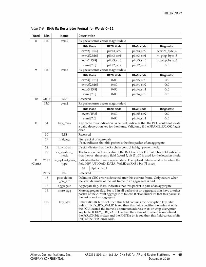
PRELIMINARY
8 31:0 evm2 Rx packet error vector magnitude 2
Bits Mode HT20 Mode HT40 Mode Diagnostic
evm2[31:24] pilot3_str2 pilot3_str2 service_byte_4
evm2[23:16] pilot3_str1 pilot3_str1 ht_plcp_byte_5
evm2[15:8] pilot3_str0 pilot3_str0 ht_plcp_byte_6
evm2[7:0] pilot2_str2 pilot2_str2 0x0
9 31:0 evm3 Rx packet error vector magnitude 3
Bits Mode HT20 Mode HT40 Mode Diagnostic
evm3[31:24] 0x80 pilot5_str0 0x0
evm3[23:16] 0x80 pilot4_str2 0x0
evm3[15:8] 0x80 pilot4_str1 0x0
evm3[7:0] 0x80 pilot4_str0 0x0
10 31:16 RES Reserved
15:0 evm4 Rx packet error vector magnitude 4
Bits Mode HT20 Mode HT40 Mode Diagnostic
evm4[15:8] 0x80 pilot5_str2 0x0
evm4[7:0] 0x80 pilot4_str1 0x0
11 31 key_miss Key cache miss indication. When set, indicates that the PCU could not locate a valid decryption key for the frame. Valid only if the FRAME_RX_OK flag is clear.
30 RES Reserved
29 first_agg First packet of aggregate If set, indicates that this packet is the first packet of an aggregate.
28 hi_rx_chain If set indicates that the Rx chain control in high power mode.
27 rx_location_ mode
The location mode indicator of the Rx Descriptor Format. This field indicates that the rcv_timestamp field (word 3, bit [31:0]) is used for the location mode.
11 (Cont.)
26:25 hw_upload_data_type
Indicates the hardware upload data. The upload data is valid only when the field HW_UPLOAD_DATA_VALID at RXS 4 bit [7] is set:
01 Upload is H
24:19 RES Reserved
18 post_delim_crc_err
Delimiter CRC error is detected after this current frame. Only occurs when the start delimiter of the last frame in an aggregate is bad.
17 aggregate Aggregate flag. If set, indicates that this packet is part of an aggregate.
16 more_agg More aggregate flag. Set to 1 in all packets of an aggregate that have another packet of the current aggregate to follow. If clear, indicates that this packet is the last one of an aggregate.
15:9 key_idx If the FrRxOK bit is set, then this field contains the decryption key table index. If KEY_IDX_VALID is set, then this field specifies the index at which the PCU located the frame’s destination address in its on-chip decryption key table. If KEY_IDX_VALID is clear, the value of this field is undefined. If the FrRxOK bit is clear and the PHYErr bit is set, then this field contains bits [7:1] of the PHY error code.
Table 3-6. DMA Rx Descriptor Format for Words 0–11
Word Bits Name Description
Atheros Communications, Inc. AR9331 802.11n 1x1 2.4 GHz SoC for AP and Router Platforms • 45 COMPANY CONFIDENTIAL December 2010 • 45

PRELIMINARY
11 (Cont.)
8 key_idx_valid If FRAME_RX_OK is set, this field contains the decryption key table index valid flag. If set, indicates that the PCU successfully located the frame's source address in its on-chip key table and that the KEY_IDX field reflects the table index at which the destination address was found. If clear, indicates that PCU failed to locate the destination address in the key table and that the contents of KeyIdx field are undefined. If the FRAME_RX_OK bit is clear and the PHY_ERROR bit is set, then this field contains bit [0] of the PHY error code.
7 aspd_trig Received APSD trigger frame.. The received frame matched the profile of an APSD trigger frame.
6 pre_delim_crc_err
Delimiter CRC error detected before this current frame. May indicate that an entire packet may have been lost.
5 mic_error Michael integrity check error flag. If set, then the frame TKIP Michael integrity check value did not verify correctly. Valid only when all of the following are true:■ FRAME_RX_OK bit is set■ The frame was decrypted using TKIP key type■ The frame is not a fragment
4 phy_error PHY error flag. If set, then reception of the frame failed because the PHY encountered an error. In this case, bits [15:8] of this word indicate the specific type of PHY error; see the baseband specification for details. Valid only if the FRAME_RX_OK flag is clear.
3 decrypt_crc_err Decryption CRC failure flag. If set, reception of the frame failed because the frame was marked as encrypted but the PCU was unable to decrypt the frame properly because the CRC check failed after the decryption process completed. Valid only if the FRAME_RX_OK flag is clear.
2 crc_error CRC error flag. If set, reception of the frame failed because the PCU detected an incorrect CRC value. Valid only if the FRAME_RX_OK flag is clear.
1 frame_rx_ok Frame reception success flag. If set, the frame was received successfully. If clear, an error occurred during frame reception.
0 done Descriptor completion flag. Set to one by the DMA engine when it has finished processing the descriptor and has updated the status information. Valid for all descriptors.
Table 3-6. DMA Rx Descriptor Format for Words 0–11
Word Bits Name Description
46 • AR9331 802.11n 1x1 2.4 GHz SoC for AP and Router Platforms Atheros Communications, Inc. 46 • December 2010 COMPANY CONFIDENTIAL
PRELIMINARY
3.4 Queue Control Unit (QCU)The queue control unit performs two tasks:
■ Managing the Tx descriptor chain processing for frames pushed to the QCU from the host by traversing the linked list of Tx descriptors and transferring frame data from the host to the targeted DCU.
■ Managing the queue transmission policy to determine when the frame at the head of the queue should be marked as available for transmission.
The MAC contains ten QCUs. Each QCU contains all the logic and state registers needed to manage a single queue (linked list) of Tx descriptors. A QCU is associated with exactly one DCU. When a QCU prepares a new frame, it signals ready to the DCU. When the DCU accepts the frame, the QCU responds by getting the frame data and passing it to the DCU for eventual transmission to the PCU and on to the air.
The host controls how the QCU performs these tasks by writing to various QCU configuration registers.
3.5 DCF Control Unit (DCU)Collectively, the ten DCUs implement the EDCF channel access arbitration mechanism defined in the Task Group E (TGe) QoS extension to the 802.11 specification. Each DCU is associated with one of the eight EDCF priority levels and arbitrates with the other DCUs on behalf of all QCUs associated with it. A central DCU arbiter monitors the state of all DCUs and grants one the next access to the PCU (that is, access to the channel).
Because the EDCF standard defines eight priority levels, the first eight DCUs (DCUs 0–7) map directly to the eight EDCF priority levels. The two additional DCUs handle beacons and beacon-gated frames for a total of ten DCUs.
The mapping of physical DCUs to absolute channel access priorities is fixed and cannot be altered by software:
The highest-priority DCU is DCU 9. Typically, this DCU is the one associated with beacons.
The next highest priority DCU is DCU 8. Typically, this DCU is the one associated with beacon-gated frames.
The remaining eight DCUs priority levels are filled with DCUs 7 through 0. Among these 8 DCUs, DCU 7 has highest priority, DCU 6 the next highest priority, and so on through DCU 0, which has the lowest priority. Typically, these DCUs are associated with EDCF priorities seven through zero, respectively.
Atheros Communications, Inc. AR9331 802.11n 1x1 2.4 GHz SoC for AP and Router Platforms • 47 COMPANY CONFIDENTIAL December 2010 • 47

PRELIMINARY
3.5.1 DCU State InformationEach DCU maintains sufficient state information to implement EDCF channel arbitration. Table 3-7 lists basic DCU state registers. (See “DCF Control Unit (DCU)” on page 47).
3.6 Protocol Control Unit (PCU)The PCU is responsible for the details of sending a frame to the baseband logic for transmission, for receiving frames from the baseband logic and passing the frame data to the DRU, including:■ Buffering Tx and Rx frames■ Encrypting and decrypting■ Generating ACK, RTS, and CTS frames■ Maintaining the timing synchronization
function (TSF)■ Forming aggregate
■ Maintaining sequence state and generating Block ACK.
■ Inserting and verifying FCS ■ Generating virtual clear channel assessment
(CCA)■ Updating and parsing beacons■ The PCU is primarily responsible for
buffering outgoing and incoming frames and conducting medium access compatible with the IEEE 802.11 DCF protocol.
Figure 3-1 shows the PCU functional block diagram.
Table 3-7. DCU Registers
Register Size Page
“QCU Mask (D_QCUMASK)” 32 page 132
“Retry Limits (D_RETRY_LIMIT)” 32 page 133
“ChannelTime Settings (D_CHNTIME)” 32 page 134
“Misc. DCU-Specific Settings (D_MISC)” 32 page 134
“DCU-Global IFS Settings: SIFS Duration (D_GBL_IFS_SIFS)” 32 page 135
“DCU-Global IFS Settings: Slot Duration (D_GBL_IFS_SLOT)” 32 page 135
“DCU-Global IFS Settings: EIFS Duration (D_GBL_IFS_EIFS)” 32 page 135
“DCU-Global IFS Settings: Misc. Parameters (D_GBL_IFS_MISC)” 32 page 136
“DCU Tx Pause Control/Status (D_TXPSE)” 32 page 136
“DCU Transmission Slot Mask (D_TXSLOTMASK)” 32 page 137
Figure 3-2. PCU Functional Block Diagram
Tx FIFO / BeaconStore 1 K x 32-BitWord (4 K bytes)
WEP/TKIP/AES Engine
Rx FIFO512 x 32-Bit Word
(2 K bytes)
Block ACK Logic
Tx State Machine
CarrierSense
Rx StateMachine
toDigital PHY
fromDigital PHY
fromDigital PHY
PCU
Inte
rnal
Bus
Inte
rfac
ean
dRe
gist
ersfrom
DCU
toDRU
Configuration
48 • AR9331 802.11n 1x1 2.4 GHz SoC for AP and Router Platforms Atheros Communications, Inc. 48 • December 2010 COMPANY CONFIDENTIAL

PRELIMINARY
4. Digital PHY BlockThe digital physical layer (PHY) block is described in 802.11n mode and 802.11b/g legacy mode. Transmit and receive paths are provided and shown as block diagrams for 802.11n mode.
4.1 OverviewThe digital PHY block is a half-duplex, OFDM, CCK, DSSS baseband processor compatible with IEEE 802.11n and 802.11b/g. The AR9331 supports PHY data rates up to 150Mbps in the 40 MHz channel mode and all data rates defined by the IEEE 802.11b/g standard (1–54Mbps). Modulation schemes include BPSK, QPSK, 16-QAM, 64-QAM and forward error correction coding with rates of 1/2, 2/3, 3/4, 5/6.
4.2 802.11n Mode Frames beginning with training symbols are used for signal detection, automatic gain control, frequency offset estimation, symbol timing, and channel estimation. This process uses 56 sub-carriers for 20 MHz HT mode: 52 for data transmission and 4 for pilots. It uses 114 sub-carriers for 40 MHz HT mode: 108 for data transmission and 6 for pilots.
4.2.1 Transmitter (Tx)Figure 4-1 shows the Tx path digital PHY 802.11n block diagram.
The PCU block initiates transmission. The digital PHY powers on the digital to analog converter (DAC) and transmit portions of the AR9331. The training symbols are a fixed waveform and are generated within the digital PHY in parallel with the PCU sending the Tx header (frame length, data rate, etc.). The PCU must send transmitted data quickly enough to prevent buffers in the digital PHY from becoming empty. The PCU is prevented from sending data too quickly by pauses generated within the digital PHY.Figure 4-1 shows a system with one spatial data stream. Puncturing and padding are added to the encoded data. At this point, it interleaves coded bits across different data subcarriers followed by the modulation, then the stream undergoes IFFT processing to produce time domain signals.
4.2.2 Receiver (Rx)Figure 4-2 shows the Rx path digital PHY 802.11n block diagram.
The receiver inverts the transmitter’s steps, performing a fast fourier transform (FFT), extracting bits from received constellations, de-interleaving, accounting for puncturing, decoding, and descrambling. The Rx block shows two spatial streams configuration. Figure 4-2 shows a frequency-domain equalizer handling degradation due to multi-path.
Figure 4-1. Digital PHY 802.11n Tx
Figure 4-2. Digital PHY 802.11n Rx
Atheros Communications, Inc. AR9331 802.11n 1x1 2.4 GHz SoC for AP and Router Platforms • 49 COMPANY CONFIDENTIAL December 2010 • 49
PRELIMINARY
4.3 802.11b/g Legacy Mode
4.3.1 TransmitterThe AR9331 digital PHY incorporates an OFDM and DSSS transceiver that supports all data rates defined by IEEE 802.11b/g. Legacy mode is detected on per-frame basis. PLCP frames are detected for legacy network information. The transmitter switches dynamically to generate legacy signals.
4.3.2 Receiver The receiver is capable of dynamically detecting legacy, HT 20 MHz or 40 MHz frames and will demodulate the frame according to the detected frame type.
50 • AR9331 802.11n 1x1 2.4 GHz SoC for AP and Router Platforms Atheros Communications, Inc. 50 • December 2010 COMPANY CONFIDENTIAL
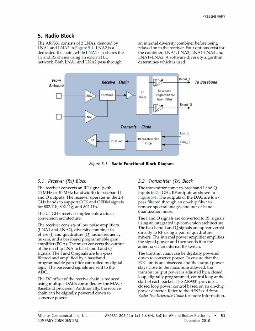
PRELIMINARY
5. Radio BlockThe AR9331 consists of 2 LNAs, denoted by LNA1 and LNA2 in Figure 5-1. LNA2 is a dedicated Rx chain, while LNA1/Tx shares the Tx and Rx chains using an external LC network. Both LNA1 and LNA2 pass through
an internal diversity combiner before being relayed on to the receiver. Four options exist for the combiner; LNA1, LNA2, LNA1-LNA2 and LNA1+LNA2. A software diversity algorithm determines which is used.
5.1 Receiver (Rx) BlockThe receiver converts an RF signal (with 20 MHz or 40 MHz bandwidth) to baseband I and Q outputs. The receiver operates in the 2.4 GHz bands to support CCK and OFDM signals for 802.11b, 802.11g, and 802.11n.
The 2.4 GHz receiver implements a direct conversion architecture.
The receiver consists of low noise amplifiers (LNA1 and LNA2), diversity combiner in-phase (I) and quadrature (Q) radio frequency mixers, and a baseband programmable gain amplifier (PGA). The mixer converts the output of the on-chip LNA to baseband I and Q signals. The I and Q signals are low-pass filtered and amplified by a baseband programmable gain filter controlled by digital logic. The baseband signals are sent to the ADC.
The DC offset of the receive chain is reduced using multiple DACs controlled by the MAC/Baseband processor. Additionally, the receive chain can be digitally powered down to conserve power.
5.2 Transmitter (Tx) BlockThe transmitter converts baseband I and Q inputs to 2.4 GHz RF outputs as shown in Figure 5-1. The outputs of the DAC are low-pass filtered through an on-chip filter to remove spectral images and out-of-band quantization noise.
The I and Q signals are converted to RF signals using an integrated up-conversion architecture. The baseband I and Q signals are up-converted directly to RF using a pair of quadrature mixers. The internal power amplifier amplifies the signal power and then sends it to the antenna via an internal RF switch.
The transmit chain can be digitally powered down to conserve power. To ensure that the FCC limits are observed and the output power stays close to the maximum allowed, the transmit output power is adjusted by a closed loop, digitally programmed, control loop at the start of each packet. The AR9331 provides a closed loop power control based on an on-chip power detector. Refer to the AR92xx Atheros Radio Test Reference Guide for more Information.
Figure 5-1. Radio Functional Block Diagram
Atheros Communications, Inc. AR9331 802.11n 1x1 2.4 GHz SoC for AP and Router Platforms • 51 COMPANY CONFIDENTIAL December 2010 • 51

PRELIMINARY
5.3 Synthesizer (SYNTH) BlockThe radio supports one on-chip synthesizer to generate local oscillator (LO) frequencies for the receiver and transmitter mixers. The synthesizer is a fractional -N synthesizer, and its topology is shown in Figure 5-2.
The AR9331 generates the reference input from a 40 MHz crystal for the synthesizer. An on-chip voltage controlled oscillator (VCO) provides the desired LO signal based on a phase/frequency locked loop.
Upon power up or channel reselection, the synthesizer takes approximately 0.2 ms to settle.
5.4 Bias/Control (BIAS) BlockThe bias/control block provides the reference voltages and currents for all other circuit blocks (see Figure 5-3). An on-chip bandgap reference circuit provides the needed voltage and current references based on an internal bias resistor.
Figure 5-2. Radio Synthesizer Block Diagram
Figure 5-3. Bias/Control Block Diagram
52 • AR9331 802.11n 1x1 2.4 GHz SoC for AP and Router Platforms Atheros Communications, Inc. 52 • December 2010 COMPANY CONFIDENTIAL

PRELIMINARY
6. Register DescriptionsThese sections describe the internal registers for the various AR9331 blocks. The AR9331 has two types of registers:
■ Registers directly memory mapped to the CPU address space (see Table 6-1).
■ Registers indirectly mapped through the MDIO interface of GE0. All the Ethernet Switch related registers fall in this category (see “PHY Control Registers” on page 262).
Table 6-1 summarizes the CPU mapped registers for the AR9331.
Table 6-1. CPU Mapped Registers Summary
Address Description Page
0x18000000–0x180000A4 DDR Registers page 54
0x18020000–0x18020010 UART Registers page 60
0x18030000–0x18030004 USB Registers page 64
0x18040000–0x18040030 GPIO Registers page 65
0x18050000–0x18050044 PLL Control Registers page 70
0x18060000–0x180600B0 Reset Control Registers page 75
0x18070000 GMAC Registers page 83
0x18090000 – 0x18090024 SLIC Registers page 84
0x180A0000–0x180A005C MBOX Registers page 88
0x180B0000–0x180B001C I2S Registers page 98
0x180B8000–0x180B8020 MDIO Slave Registers page 102
0x18100008–0x181000DC General DMA and Rx-Related Registers page 125
0x18100800 + (Q<<2) – 0x18100A44 QCU Registers page 125
0x18101000 + (D<<2) – 0x181012F0 DCU Registers page 132
0x18104000–0x181040D4 Host Interface Registers page 138
0x18107040–0x18107058 RTC Interface Registers page 151
0x18108000–0x181088F4 MAC PCU Registers page 156
0x19000000–0x190001D8 0x1A000000–0x1A0001D8
Ethernet Registers page 195
0x1B000100–0x1B0001D4 USB Controller Registers page 231
0x1F000000–0x1F00000C Serial Flash Registers page 261
Table 6-2. Ethernet Switch and PHY Registers
Address Description Page
0x00 PHY Control Registers page 262
0x00 Ethernet Switch/Global Control Registers page 282
0x00 Ethernet Switch/Port Control Registers page 294
Atheros Communications, Inc. AR9331 802.11n 1x1 2.4 GHz SoC for AP and Router Platforms • 53 COMPANY CONFIDENTIAL December 2010 • 53

PRELIMINARY
6.1 DDR RegistersTable 6-3 summarizes the DDR registers for the AR9331.
6.1.1 DRR DRAM Configuration (DDR_CONFIG)Address: 0x18000000 Access: Read/Write Reset: See field description
This register is used to configure the DDR DRAM parameters.
Table 6-3. DDR Registers Summary
Address Name Description Page0x18000000 DDR_CONFIG DDR DRAM Configuration page 540x18000004 DDR_CONFIG2 DDR DRAM Configuration 2 page 550x18000008 DDR_MODE_REGISTER DDR Mode Value page 550x1800000C DDR_EXTENDED_MODE_REGISTER DDR Extended Mode Value page 550x18000010 DDR_CONTROL DDR Control page 560x18000014 DDR_REFRESH DDR Refresh Control and Configuration page 560x18000018 DDR_RD_DATA_THIS_CYCLE DDR Read Data Capture Bit Mask page 560x1800001C TAP_CONTROL_0 DQS Delay Tap Control for Byte 0 page 560x18000020 TAP_CONTROL_1 DQS Delay Tap Control for Byte 1 page 570x1800007C DDR_WB_FLUSH_GE0 GE0 Interface Write Buffer Flush page 570x18000080 DDR_WB_FLUSH_GE1 GE1 Interface Write Buffer Flush page 570x18000084 DDR_WB_FLUSH_USB USB Interface Write Buffer Flush page 570x1800008C DDR_DDR2_CONFIG DDR2 Configuration page 580x18000090 DDR_EMR2 DDR Extended Mode 2 Value page 580x18000094 DDR_EMR3 DDR Extended Mode 3 Value page 580x18000098 DDR_BURST DDR Burst Control page 590x1800009C AHB_MASTER_TIMEOUT_MAX AHB Master Timeout Control page 590x180000A0 AHB_MASTER_TIMEOUT_CURNT AHB Timeout Current Count page 590x180000A4 AHB_MASTER_TIMEOUT_SLAVE_ADDR Timeout Slave Address page 59
Bit Bit Name Reset Description31 CAS_LATENCY_MSB 0x0 MSB bit of a 4-bit CAS_LATENCY field30 OPEN_PAGE 0x1 Controller open page policy. This policy increases bus efficiency if
accesses are local to a page but increase random read/write latency.0 Page open1 Page closed
29:27 CAS_LATENCY 0x6 DRAM CAS latency parameter (first 3 bits) rounded up in memory core clock cycles. Used by the hardware to estimate the internal DDR clock latency of a read. It should be > GATE_OPEN_LATENCY as specified in the DDR_CONFIG2 register. The value of this register should be Memory CAS_LATENCY * 2 or CAS_LATENCY * 2+1/2/3.
26:23 TMRD 0xF DRAM tMRD parameter rounded up in memory core clock cycles22:17 TRFC 0x1F DRAM tRFC parameter rounded up in memory core clock cycles16:13 TRRD 0x4 DRAM tRRD parameter rounded up in memory core clock cycles12:9 TRP 0x6 DRAM tRP parameter rounded up in memory core clock cycles8:5 TRCD 0x6 DRAM tRCD parameter rounded up in memory core clock cycles4:0 TRAS 0x10 DRAM tRAS parameter rounded up in memory core clock cycles
54 • AR9331 802.11n 1x1 2.4 GHz SoC for AP and Router Platforms Atheros Communications, Inc. 54 • December 2010 COMPANY CONFIDENTIAL

PRELIMINARY
6.1.2 DDR DRAM Configuration 2 (DDR_CONFIG2)Address: 0x18000004 Access: Read/Write Reset: See field description
GATE_OPEN_LATENCY is separated from CAS_LATENCY to separately control the write and read sides of the DQS/DQ memory inputs.
6.1.3 DDR Mode Value (DDR_MODE_REGISTER)Address: 0x18000008 Access: Read/Write Reset: See field description
This register is used to set the DDR mode register value.
6.1.4 DDR Extended Mode (DDR_EXTENDED_MODE_REGISTER)Address: 0x1800000C Access: Read/Write Reset: See field description
This register is used to set the extended DDR mode register value.
Bit Bit Name Reset Description31 HALF_WIDTH_ LOW 0x1 Controls which part of the 32-bit DDR DQ bus is populated with
DRAM in a 16-bit memory system
0 31:16
1 15:0
30 RES — Reserved
29:26 GATE_OPEN_LATENCY
0x6 Memory CAS_LATENCY * 2
25:21 TWTR 0xE DRAM tWTR parameter rounded up in memory core clock cycles
20:17 TRTP 0x8 DRAM read to precharge parameter rounded up in memory core clock cycles. The normal value is two clock cycles.
16:12 TRTW 0x10 DRAM tRTW parameter rounded up in memory core clock cycles. The value should be calculated as CAS_LATENCY + BURST_LENGTH + BUS_TURNAROUND_TIME.
11:8 TWR 0x6 DRAM tWR parameter rounded up in memory core clock cycles
7 CKE 0x1 DRAM CKE bit
6 PHASE_SELECT 0x0 Selects the output phase
5 CNTL_OE_EN 0x1 A control bit to allow the memory controller to tri-state the address/control outputs
4 BURST_TYPE 0x0 DRAM burst type
0 Sequential
1 Interleaved
3:0 BURST_LENGTH 0x8 DRAM burst length setting. (2, 4, or 8. Only 8 is supported)
Bit Bit Name Reset Description31:13 RES 0x0 Reserved. Must be written with zero. Contains zeros when read.
12:0 VALUE 0x133 Mode register value. Reset to CAS 3, BL=8, sequential, DLL reset off.
Bit Bit Name Reset Description31:13 RES 0x0 Reserved. Must be written with zero. Contains zeros when read.
12:0 VALUE 0x2 Extended mode register value. Reset to weak driver, DLL on.
Atheros Communications, Inc. AR9331 802.11n 1x1 2.4 GHz SoC for AP and Router Platforms • 55 COMPANY CONFIDENTIAL December 2010 • 55

PRELIMINARY
6.1.5 DDR Control (DDR_CONTROL)Address: 0x18000010 Access: Read/Write Reset: 0x0
This register is used to force update cycles in the DDR control.
6.1.6 DDR Refresh Control and Configuration (DDR_REFRESH)Address: 0x18000014 Access: Read/Write Reset: See field description
This register is used to configure the settings to refresh the DDR,
6.1.7 DDR Read Data Capture Bit Mask (DDR_RD_DATA_THIS_CYCLE)Address: 0x18000018 Access: Read/Write Reset: See field description
This register is used to set the parameters to read the DDR and capture bit masks.
6.1.8 DQS Delay Tap Control for Byte 0 (TAP_CONTROL_0)Address: 0x1800001C Access: Read/Write Reset: See field descriptions
This register is used along with DQ Lane 0, DQ[7:0], DQS_0.
Bit Bit Name Description31:6 RES Reserved
5 EMR3 Forces an EMR3S update cycle
4 EMR2 Forces an EMR2S update cycle
3 PREA Forces a PRECHARGE ALL cycle
2 REF Forces an AUTO REFRESH cycle
1 EMRS Forces an EMRS update cycle
0 MRS Forces an MRS update cycle
Bit Bit Name Reset Description31:15 RES 0x0 Reserved
14 ENABLE 0x0 Setting this bit will enable a DDR refresh
13:0 PERIOD 0x12C Sets the refresh period intervals
Bit Bit Name Reset Description31:24 RES 0x0 Reserved. Must be written with zero. Contains zeros when read.
23:0 VEC 0xFF DDR read and capture bit mask. Each bit represents a cycle of valid data.
Bit Bit Name Reset Description31:17 RES 0x0 Reserved
16 TAP_H_ BYPASS 0x0 Set to 1 to bypass the higher 32-level delay chain
15:13 RES 0x0 Reserved
12:8 TAP_H 0x0 Tap setting for higher 32-level delay chain
6:5 RES 0x0 Reserved
4:0 TAP_L 0x5 Tap setting for lower 32-level delay chain
56 • AR9331 802.11n 1x1 2.4 GHz SoC for AP and Router Platforms Atheros Communications, Inc. 56 • December 2010 COMPANY CONFIDENTIAL

PRELIMINARY
6.1.9 DQS Delay Tap Control for Byte 1 (TAP_CONTROL_1)Address: 0x18000020 Access: Read/Write Reset: See field descriptions
This register is used along with DQ Lane 1, DQ[15:8], DQS_1.
6.1.10 GE0 Interface Write Buffer Flush (DDR_WB_FLUSH_GE0)Address: 0x1800007C Access: Read/Write Reset: 0x0
This register is used to flush the write buffer for the GE0 interface.
6.1.11 GE1 Interface Write Buffer Flush (DDR_WB_FLUSH_GE1)Address: 0x18000080 Access: Read/Write Reset: 0x0
This register is used to flush the write buffer for the GE1 interface.
6.1.12 USB Interface Write Buffer Flush (DDR_WB_FLUSH_USB)Address: 0x18000084 Access: Read/Write Reset: 0x0
This register is used to flush the write buffer for the USB interface.
Bit Bit Name Reset Description
31:17 RES 0x0 Reserved
16 TAP_H_ BYPASS 0x0 Set to 1 to bypass the higher 32-level delay chain
15:13 RES 0x0 Reserved
12:8 TAP_H 0x5 Tap setting for higher 32-level delay chain
7:5 RES 0x0 Reserved
4:0 TAP_L 0x5 Tap setting for lower 32-level delay chain
Bit Bit Name Description
31:1 RES Reserved. Must be written with zero. Contains zeros when read.
0 FLUSH Set this bit to 1 to flush the write buffer for the GE0 interface. This bit will reset to 0 when the flush is complete.
Bit Bit Name Type Reset Description
31:1 RES RO 0x0 Reserved. Must be written with zero. Contains zeros when read.
0 FLUSH RW 0x0 Set this bit to 1 to flush the write buffer for the GE1 interface. This bit will reset to 0 when the flush is complete.
Bit Bit Name Type Reset Description
31:1 RES RO 0x0 Reserved. Must be written with zero. Contains zeros when read.
0 FLUSH RW 0x0 Set this bit to 1 to flush the write buffer for the USB interface. This bit will reset to 0 when the flush is complete.
Atheros Communications, Inc. AR9331 802.11n 1x1 2.4 GHz SoC for AP and Router Platforms • 57 COMPANY CONFIDENTIAL December 2010 • 57

PRELIMINARY
6.1.13 AMBA Interface Write Buffer Flush (DDR_WB_FLUSH_AMBA)Address: 0x18000088 Access: Read/Write Reset: 0x0
This register is used to flush the write buffer for the AMBA interface.
6.1.14 DDR2 Configuration (DDR_DDR2_CONFIG)Address: 0x1800008C Access: Read/Write Reset: 0x0858
6.1.15 DDR EMR2 (DDR_EMR2)Address: 0x18000090 Access: Read/Write Reset: 0x0
This register is used set the extended mode register 2 value.
6.1.16 DDR EMR3 (DDR_EMR3)Address: 0x18000094 Access: Read/Write Reset: 0x0
This register is used set the extended mode register 3 value.
Bit Bit Name Type Reset Description
31:1 RES RO 0x0 Reserved. Must be written with zero. Contains zeros when read.
0 FLUSH RW 0x0 Set this bit to 1 to flush the write buffer for the AMBA interface. This bit will reset to 0 when the flush is complete.
Bit Bit Name Type RW Description
31:13 RES RO 0x0 Reserved
12:10 DDR2_TWL RW 0x0 Delay between WE_l/CAS_L assertion on DQS, DQ assertion for a DDR2 write transaction (in DDR_CLK cycles)
9:8 RES RO 0x0 Reserved
7:2 DDR2_TFAW RW 0x16 tFAW parameter in core DDR_CLK cycles
1 RES RW 0x0 Reserved
0 ENABLE_DDR RW 0x0 0 DDR1
1 DDR2
Bit Bit Name Type Reset Description
31:13 RES RO 0x0 Reserved. Must be written with zero. Contains zeros when read.
12:0 VALUE RW 0x0 Extended mode register 2 value
Bit Bit Name Type Reset Description
31:13 RES RO 0x0 Reserved. Must be written with zero. Contains zeros when read.
12:0 VALUE RW 0x0 Extended mode register 2 value
58 • AR9331 802.11n 1x1 2.4 GHz SoC for AP and Router Platforms Atheros Communications, Inc. 58 • December 2010 COMPANY CONFIDENTIAL
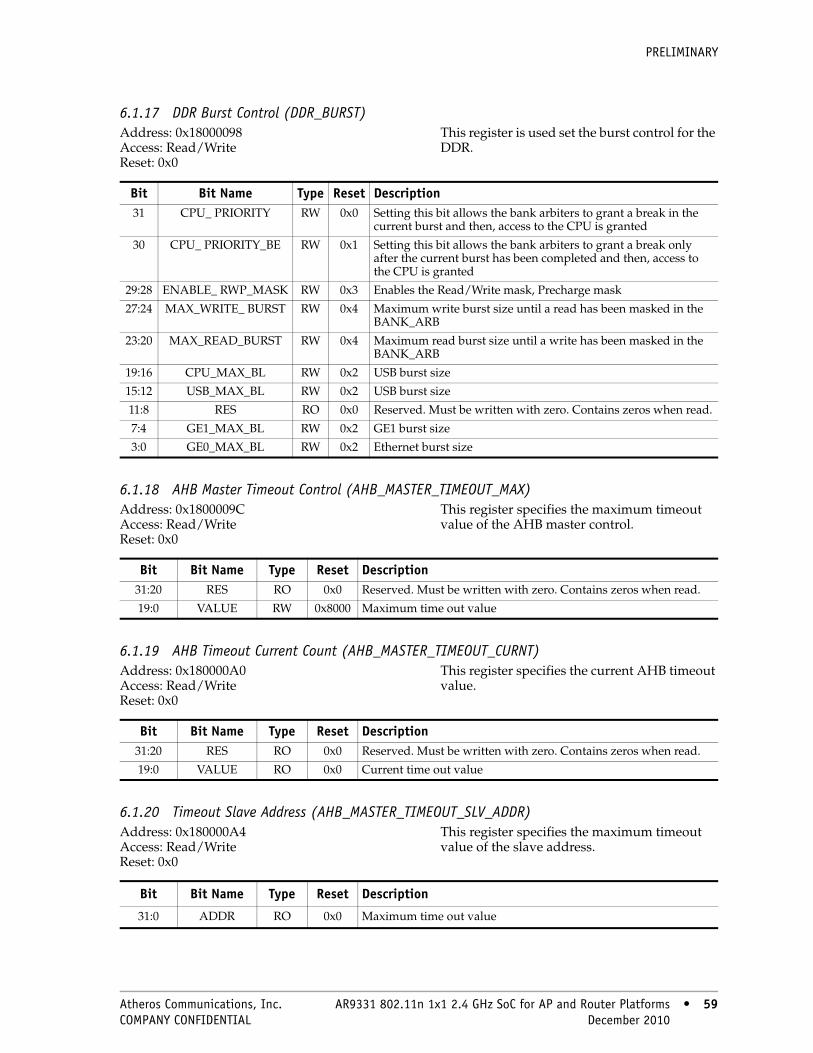
PRELIMINARY
6.1.17 DDR Burst Control (DDR_BURST)Address: 0x18000098 Access: Read/Write Reset: 0x0
This register is used set the burst control for the DDR.
6.1.18 AHB Master Timeout Control (AHB_MASTER_TIMEOUT_MAX)Address: 0x1800009C Access: Read/Write Reset: 0x0
This register specifies the maximum timeout value of the AHB master control.
6.1.19 AHB Timeout Current Count (AHB_MASTER_TIMEOUT_CURNT)Address: 0x180000A0 Access: Read/Write Reset: 0x0
This register specifies the current AHB timeout value.
6.1.20 Timeout Slave Address (AHB_MASTER_TIMEOUT_SLV_ADDR)Address: 0x180000A4 Access: Read/Write Reset: 0x0
This register specifies the maximum timeout value of the slave address.
Bit Bit Name Type Reset Description31 CPU_ PRIORITY RW 0x0 Setting this bit allows the bank arbiters to grant a break in the
current burst and then, access to the CPU is granted
30 CPU_ PRIORITY_BE RW 0x1 Setting this bit allows the bank arbiters to grant a break only after the current burst has been completed and then, access to the CPU is granted
29:28 ENABLE_ RWP_MASK RW 0x3 Enables the Read/Write mask, Precharge mask
27:24 MAX_WRITE_ BURST RW 0x4 Maximum write burst size until a read has been masked in the BANK_ARB
23:20 MAX_READ_BURST RW 0x4 Maximum read burst size until a write has been masked in the BANK_ARB
19:16 CPU_MAX_BL RW 0x2 USB burst size
15:12 USB_MAX_BL RW 0x2 USB burst size
11:8 RES RO 0x0 Reserved. Must be written with zero. Contains zeros when read.
7:4 GE1_MAX_BL RW 0x2 GE1 burst size
3:0 GE0_MAX_BL RW 0x2 Ethernet burst size
Bit Bit Name Type Reset Description31:20 RES RO 0x0 Reserved. Must be written with zero. Contains zeros when read.
19:0 VALUE RW 0x8000 Maximum time out value
Bit Bit Name Type Reset Description31:20 RES RO 0x0 Reserved. Must be written with zero. Contains zeros when read.
19:0 VALUE RO 0x0 Current time out value
Bit Bit Name Type Reset Description
31:0 ADDR RO 0x0 Maximum time out value
Atheros Communications, Inc. AR9331 802.11n 1x1 2.4 GHz SoC for AP and Router Platforms • 59 COMPANY CONFIDENTIAL December 2010 • 59

PRELIMINARY
6.2 UART RegistersTable 6-6 summarizes the UART registers for the AR9331.
6.2.1 UART Transmit and Rx FIFO Interface (UART_DATA)Address: 0x18020000 Access: Read/Write Reset: 0x0
This register pushes data on the Tx FIFO and pop data off the Rx FIFO. This interface can be used only if all other interfaces are disabled in the “UART Configuration and Status (UART_CS)” on page 61.
Table 6-4. UART Registers Summary
Address Name Description Page
0x18020000 UART_DATA UART Transmit and Rx FIFO page 60
0x18020004 UART_CS UART Configuration and Status page 61
0x18020008 UART_CLOCK UART Clock page 62
0x1804000C UART_INT UART Interrupt page 62
0x18040010 UART_INT_EN UART Interrupt Enable page 63
Bit Bit Name Type Reset Description
31:10 RES RO 0x0 Reserved. Must be written with zero. Contains zeros when read.
9 UART_TX_ CSR
RW 0x0 Read returns the status of the Tx FIFO. If set, the Tx FIFO can accept more transmit data. Setting this bit will push UART_TX_RX_DATA on the Tx FIFO. Clearing this bit has no effect.
8 UART_RX_ CSR
RW 0x0 Read returns the status of the Rx FIFO. If set, the receive data in UART_TX_RX_DATA is valid. Setting this bit will pop the Rx FIFO if there is valid data. Clearing this bit has no effect.
7:0 UART_TX_ RX_DATA
RW 0x0 Read returns receive data from the Rx FIFO, but leaves the FIFO unchanged. The receive data is valid only if UART_RX_CSR is also set. Write pushes the transmit data on the Tx FIFO if UART_TX_CSR is also set.
60 • AR9331 802.11n 1x1 2.4 GHz SoC for AP and Router Platforms Atheros Communications, Inc. 60 • December 2010 COMPANY CONFIDENTIAL

PRELIMINARY
6.2.2 UART Configuration and Status (UART_CS)Address: 0x18020004 Access: Read/Write Reset: See field description
This register configures the UART operation and reports the operating status.
Bit Bit Name Type Reset Description31:16 RES RO 0x0 Reserved. Must be written with zero. Contains zeros when read.
15 UART_RX_ BUSY
R — This bit is set whenever there is receive data or data is being received. It is clear when receive is completely idle.
14 UART_TX_ BUSY
R — This bit is set whenever there is data ready to transmit or being transmitted. It is clear when transmit is completely idle.
13 UART_ HOST_INT_EN
RW 0x0 Enables an interrupt on the UART host
12 UART_HOST_ INT
R — This bit will be set while the host interrupt is being asserted and will clear when host interrupt is deasserted.
11 UART_TX_ BREAK
RW 0x0 This bit blocks the Tx FIFO and causes a break to be continuously transmitted. The Tx FIFO will resume normal operation when this bit is clear.
10 UART_RX_ BREAK
R — This bit will be set while a break is being received. It will clear when the receive break stops.
9 UART_SERIAL_TX_READY
R — This bit will be set while Serial Tx Ready is asserted and is cleared when Serial Tx Ready is deasserted.
8 UART_TX_ READY_ORIDE
RW 0x0 This bit overrides the transmit ready flow control. If clear, transmit ready is controlled by UART_FLOW_CONTROL_MODE. If set, then transmit ready will be true.
7 UART_RX_ READY_ORIDE
RW 0x0 This bit overrides the receive ready flow control. If clear, receive ready is controlled by UART_FLOW_CONTROL_MODE. If set, then receive ready will be true.
6 UART_DMA_EN RW 0x0 Enable DMA interface mode. If this is set, then transmit and Rx FIFO access through “UART Transmit and Rx FIFO Interface (UART_DATA)” on page 60 is disabled. Instead, these FIFOs are connected to the internal DMA interface, if available.
5:4 UART_FLOW_ CONTROL_
MODE
RW 0x0 Select which hardware flow control to enable
00 No flow control. Disable hardware flow control. Serial Transmit Ready and Serial Receive Ready are controlled by UART_RX_READY_ORIDE and UART_TX_READY_ORIDE.
10 Hardware flow control. Enable standard RTS/CTS flow control to control Serial Transmit Ready and Serial Receive Ready.
11 Inverted Flow Control. Enable inverted RTS/CTS flow control to control Serial Transmit Ready and Serial Receive Ready
3:2 UART_ INTERFACE_
MODE
RW 0x0 Select which serial port interface to enable
00 No interface. Disable serial port.
01 DTE interface. Configure serial port for DTE (Data Terminal Equipment) operation. Transmit on TD, receive on RD, flow control out on RTS, flow control in on CTS.
10 DCE interface. Configure serial port for DCE (Data Communication Equipment) operation. Transmit on RD, receive on TD, flow control out on CTS, flow control in on RTS.
1:0 UART_PARITY_MODE
RW 0x0 Select the parity mode for transmit and receive data
00 No parity. Parity is not transmitted or received
10 Odd parity. Odd parity is transmitted and checked on receive
11 Even parity. Even parity is transmitted and checked on receive
Atheros Communications, Inc. AR9331 802.11n 1x1 2.4 GHz SoC for AP and Router Platforms • 61 COMPANY CONFIDENTIAL December 2010 • 61

PRELIMINARY
6.2.3 UART Clock (UART_CLOCK)Address: 0x18020008 Access: Read/Write Reset: 0x0
This register sets the scaling factors use by the serial clock interpolator to create the transmit bit clock and receive sample clock.
6.2.4 UART Interrupt/Control Status (UART_INT)Address: 0x1802000C Access: Read/Write Reset: See field description
This register when read, returns the current interrupt status. Setting a bit will clear the individual attempt. Clearing a bit has no effect.
Bit Bit Name Type Reset Description31:24 RES RO 0x0 Reserved. Must be written with zero. Contains zeros when read.
23:16 UART_ CLOCK_ SCALE
RW 0x0 The serial clock divisor used to create a scaled Serial Clock. This is used to bring the serial clock into a range that can be interpolated by UART_CLOCK_STEP. The actual divisor is (1 + UART_CLOCK_SCALE). Use the formula:UART_CLOCK_SCALE = truncate(((1310*serialClockFreq)/(131072*baudClockFreq)))
15:0 UART_ CLOCK_STEP
RW 0x0 The ratio of the scaled serial clock to the baud clock, as expressed by a 17-bit fraction. This value should range between 1310–13107 to maintain a better than +5% accuracy. Smaller is generally better, because interpolation errors caused by a small value are far less than quantization errors caused by a large value. Use the formula:UART_CLOCK_STEP = round((131072*baudClockFreq)/(serialClockFreq/(UartClockScale+1)))
Bit Bit Name Type Reset Description31:10 RES RO 0x0 Reserved. Must be written with zero. Contains zeros when read.
9 UART_TX_ EMPTY_INT
RW 0x0 This bit will be high while the Tx FIFO is almost empty. Setting this bit will clear this interrupt. Clearing this bit has no effect.
8 UART_RX_FULL_INT
RW 0x0 This bit will be high while the Rx FIFO is almost full, triggering hardware flow control, if enabled. Setting this bit will clear this interrupt. Clearing this bit has no effect.
7 UART_RX_ BREAK_OFF_INT
RW 0x0 This bit will be high while a break is not received. Setting this bit will clear this interrupt. Clearing this bit has no effect.
6 UART_RX_ BREAK_ON_INT
RW 0x0 This bit will be high while a break is received. Setting this bit will clear this interrupt. Clearing this bit has no effect.
5 UART_RX_ PARITY_ERR_INT
RW 0x0 This bit will be high if receive parity checking is enabled and the receive parity does not match the value configured by UART_PARITY_EVEN. Setting this bit will clear this interrupt. Clearing this bit has no effect.
4 UART_TX_ OFLOW_ERR_INT
RW 0x0 This bit will be high if the Tx FIFO overflowed. Setting this bit will clear this interrupt. Clearing this bit has no effect.
3 UART_RX_ OFLOW_ERR_INT
RW 0x0 This bit will be high if the Rx FIFO overflowed. Setting this bit will clear this interrupt. Clearing this bit has no effect.
2 UART_RX_ FRAMING_ERR_
INT
RW 0x0 This bit will be high if a receive framing error was detected. Setting this bit will clear this interrupt. Clearing this bit has no effect
1 UART_TX_ READY_INT
RW 0x0 This bit will be high while there is room for more data in the Tx FIFO. Setting this bit will clear this interrupt if there is room for more data in the Tx FIFO. Clearing this bit has no effect.
0 UART_RX_VALID_INT
RW 0x0 This bit will be high while there is data in the Rx FIFO. Setting this bit will clear this interrupt if there is no more data in the Rx FIFO. Clearing this bit has no effect.
62 • AR9331 802.11n 1x1 2.4 GHz SoC for AP and Router Platforms Atheros Communications, Inc. 62 • December 2010 COMPANY CONFIDENTIAL

PRELIMINARY
6.2.5 UART Interrupt Enable (UART_INT_EN)Address: 0x18020010 Access: Read/Write Reset: See field Description
This register enables interrupts in the UART Interrupt register.
Bit Bit Name Type Reset Description
31:10 RES RO 0x0 Reserved. Must be written with zero. Contains zeros when read.
9 UART_TX_ EMPTY_INT_EN
RW 0x0 Enables UART_TX_EMPTY_INT in “UART Interrupt/Control Status (UART_INT)” on page 62.
8 UART_RX_FULL_ INT_EN
RW 0x0 Enables UART_RX_FULL_INT in “UART Interrupt/Control Status (UART_INT)” on page 62.
7 UART_RX_BREAK_OFF_INT_EN
RW 0x0 Enables UART_RX_BREAK_OFF_INT in “UART Interrupt/Control Status (UART_INT)” on page 62.
6 UART_RX_BREAK_ON_INT_EN
RW 0x0 Enables UART_RX_BREAK_ON_INT in “UART Interrupt/Control Status (UART_INT)” on page 62.
5 UART_RX_PARITY_ERR_INT_EN
RW 0x0 Enables UART_PARITY_ERR_INT in “UART Interrupt/Control Status (UART_INT)” on page 62.
4 UARTTX_OFLOW_ERR_INT_EN
RW 0x0 Enables UART_TX_OFLOW_ERR_INT in “UART Interrupt/Control Status (UART_INT)” on page 62.
3 UART_RX_OFLOW_ERR_INT_EN
RW 0x0 Enables UART_RX_OFLOW_ERR_INT in “UART Interrupt/Control Status (UART_INT)” on page 62.
2 UART_RX_ FRAMING_ERR_
INT_EN
RW 0x0 Enables UART_RX_FRAMING_ERR_INT in “UART Interrupt/Control Status (UART_INT)” on page 62.
1 UART_TX_READY_INT_EN
RW 0x0 Enables UART_TX_READY_INT in “UART Interrupt/Control Status (UART_INT)” on page 62.
0 UART_RX_VALID_ INT_EN
RW 0x0 Enables UART_RX_VALID_INT in “UART Interrupt/Control Status (UART_INT)” on page 62.
Atheros Communications, Inc. AR9331 802.11n 1x1 2.4 GHz SoC for AP and Router Platforms • 63 COMPANY CONFIDENTIAL December 2010 • 63

PRELIMINARY
6.3 USB RegistersTable 6-5 summarizes the AR9331 USB registers.
6.3.1 USB Power Control and Status (USBPWRCTL)Address: 0x18030000 Access: See field description Reset: 0x0
This register is used to set USB power and status configurations.
6.3.2 USB Configuration (USB_CONFIG)Address: 0x18030004 Access: See field description Reset: See field description
This register is used to set USB configurations.
Table 6-5. USB Registers Summary
Address Name Description Page0x18030000 USB_PWRCTL USB Power Control and Status page 540x18030004 USB_CONFIG USB Configuration page 55
Bit Bit Name Access Description31:7 RES RO Reserved. Must be written with zero. Contains zeros when read.
6 WAKEUP_ STATUS
RO Final wake-up status that wakes the USB core
5 USR_WAKEUP RW User wakeup signal. Input clears suspend output. Suspend outputs synchronize to a clock and the input does not propagate to suspend outputs until the related clock begins running. This bit must remain asserted until the related suspend output transitions to zero.
4 WAKE_OVRCURR_EN
RO Wake-up status due to a power fault
3 WAKE_ DISCNNT_EV
RO Wake-up status due to a disconnect event
2 WAKE_CNNT_ EN
RO Wake-up status due to a connect event
1 SUSPEND_CLR RO Output to notify the software of a command wake-up. This bit is not synchronized and remains set until the SUSPEND (bit [0]) clears.
0 SUSPEND RO Suspend output synchronized to the XCVR_CLK
Bit Bit Name Access Reset Description31:9 RES RW 0x0 Reserved. Must be written with zero. Contains zeros when read.
8 HOST_ONLY RW 0x1 If this bit is set to 1, the IDPULLUP input to the UTMI PHY is tied to 0 to make sure the ID signal is not sampled by the PHY
7:6 RES RW 0x0 Reserved. Must be written with zero. Contains zeros when read.
5 AHB_HRDATA_ SWAP
RW 0x1 Swap the read data on the AHB bus
4 AHB_HWDATA_SWAP
RW 0x1 Swap the hardware data on the AHB bus
3 RES RW 0x0 Reserved. Must be written with zero. Contains zeros when read.
2 HS_MODE_EN RO 0x1 Asserted when the HS interface is selected
1 UTMI_PHY_EN RO 0x0 Asserted when the UTMI interface is selected
0 RES RW 0x0 Reserved. Must be written with zero. Contains zeros when read.
64 • AR9331 802.11n 1x1 2.4 GHz SoC for AP and Router Platforms Atheros Communications, Inc. 64 • December 2010 COMPANY CONFIDENTIAL
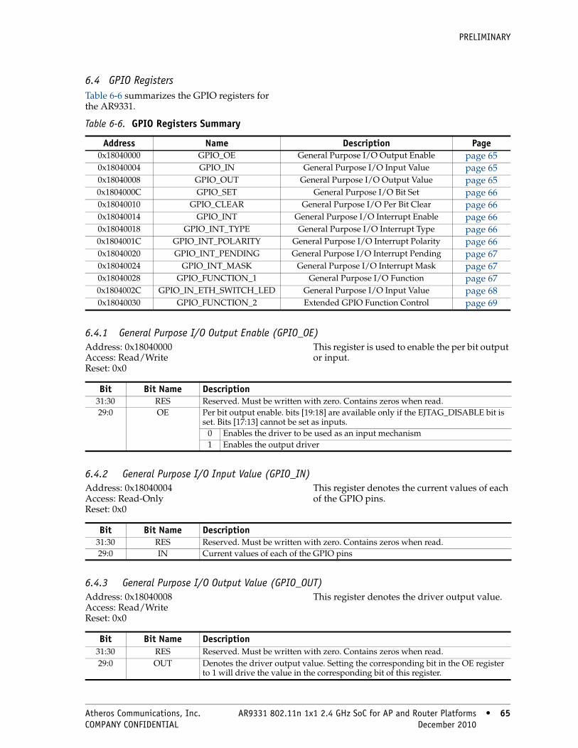
PRELIMINARY
6.4 GPIO RegistersTable 6-6 summarizes the GPIO registers for the AR9331.
6.4.1 General Purpose I/O Output Enable (GPIO_OE)Address: 0x18040000 Access: Read/Write Reset: 0x0
This register is used to enable the per bit output or input.
6.4.2 General Purpose I/O Input Value (GPIO_IN)Address: 0x18040004 Access: Read-Only Reset: 0x0
This register denotes the current values of each of the GPIO pins.
6.4.3 General Purpose I/O Output Value (GPIO_OUT)Address: 0x18040008 Access: Read/Write Reset: 0x0
This register denotes the driver output value.
Table 6-6. GPIO Registers Summary
Address Name Description Page0x18040000 GPIO_OE General Purpose I/O Output Enable page 650x18040004 GPIO_IN General Purpose I/O Input Value page 650x18040008 GPIO_OUT General Purpose I/O Output Value page 650x1804000C GPIO_SET General Purpose I/O Bit Set page 660x18040010 GPIO_CLEAR General Purpose I/O Per Bit Clear page 660x18040014 GPIO_INT General Purpose I/O Interrupt Enable page 660x18040018 GPIO_INT_TYPE General Purpose I/O Interrupt Type page 660x1804001C GPIO_INT_POLARITY General Purpose I/O Interrupt Polarity page 660x18040020 GPIO_INT_PENDING General Purpose I/O Interrupt Pending page 670x18040024 GPIO_INT_MASK General Purpose I/O Interrupt Mask page 670x18040028 GPIO_FUNCTION_1 General Purpose I/O Function page 670x1804002C GPIO_IN_ETH_SWITCH_LED General Purpose I/O Input Value page 680x18040030 GPIO_FUNCTION_2 Extended GPIO Function Control page 69
Bit Bit Name Description31:30 RES Reserved. Must be written with zero. Contains zeros when read.29:0 OE Per bit output enable. bits [19:18] are available only if the EJTAG_DISABLE bit is
set. Bits [17:13] cannot be set as inputs.0 Enables the driver to be used as an input mechanism1 Enables the output driver
Bit Bit Name Description31:30 RES Reserved. Must be written with zero. Contains zeros when read.29:0 IN Current values of each of the GPIO pins
Bit Bit Name Description31:30 RES Reserved. Must be written with zero. Contains zeros when read.29:0 OUT Denotes the driver output value. Setting the corresponding bit in the OE register
to 1 will drive the value in the corresponding bit of this register.
Atheros Communications, Inc. AR9331 802.11n 1x1 2.4 GHz SoC for AP and Router Platforms • 65 COMPANY CONFIDENTIAL December 2010 • 65

PRELIMINARY
6.4.4 General Purpose I/O Per Bit Set (GPIO_SET)Address: 0x1804000C Access: Write-Only Reset: 0x0
The bit of this register is set in response to other bits being set.
6.4.5 General Purpose I/O Per Bit Clear (GPIO_CLEAR)Address: 0x18040010 Access: Write-Only Reset: 0x0
The bit of this register is set in response to other bits being cleared.
6.4.6 General Purpose I/O Interrupt Enable (GPIO_INT)Address: 0x18040014 Access: Read/Write Reset: 0x0
The register sets the bit for interrupts into GPIO lines.
6.4.7 General Purpose I/O Interrupt Type (GPIO_INT_TYPE)Address: 0x18040018 Access: Read/Write Reset: 0x0
This register is used to set the interrupt type for GPIOs.
6.4.8 General Purpose I/O Interrupt Polarity (GPIO_INT_POLARITY)Address: 0x1804001C Access: Read/Write Reset: 0x0
This register is used to indicate the level and edge status of the GPIO interrupt.
Bit Bit Name Description31:30 RES Reserved. Must be written with zero. Contains zeros when read.29:0 SET When writing, any bit that is set will cause the corresponding GPIO bit to be set.
Any bit that is not set will have no effect.
Bit Bit Name Description31:30 RES Reserved. Must be written with zero. Contains zeros when read.29:0 CLEAR When writing, any bit that is set will cause the corresponding GPIO bit to be
cleared. Any bit that is not set will have no effect. Bits [19:18] must be set to 0x3 initially to cause these output values to be 0.
Bit Bit Name Description31:30 RES Reserved. Must be written with zero. Contains zeros when read.29:0 INT Each bit set will be considered an interrupt ORd into the GPIO interrupt line
Bit Bit Name Description31:30 RES Reserved. Must be written with zero. Contains zeros when read.29:0 TYPE Used to set the type of interrupt
0 This bit is a level-sensitive interrupt1 This bit is an edge-sensitive interrupt
Bit Bit Name Description31:30 RES Reserved. Must be written with zero. Contains zeros when read.29:0 POLARITY Each bit controls the corresponding GPIO interrupt polarity
0 Indicates that the interrupt is active low (level) or falling edge (edge)1 Indicates that the interrupt is active high (level) or rising edge (edge)
66 • AR9331 802.11n 1x1 2.4 GHz SoC for AP and Router Platforms Atheros Communications, Inc. 66 • December 2010 COMPANY CONFIDENTIAL

PRELIMINARY
6.4.9 General Purpose I/O Interrupt Pending (GPIO_INT_PENDING)Address: 0x18040020 Access: Read/Write Reset: 0x0
This register is used to indicate current pending interrupts.
6.4.10 General Purpose I/O Interrupt Mask (GPIO_INT_MASK)Address: 0x18040024 Access: Read/Write Reset: 0x0
This register is used to send interrupt messages to the central controller.
6.4.11 General Purpose I/O Function (GPIO_FUNCTION_1)Address: 0x18040028 Access: Read/Write Reset: 0x0
This register is used to enable and disable the functionality of certain multiplexed GPIO pins.
Bit Bit Name Description
31:30 RES Reserved. Must be written with zero. Contains zeros when read.
29:0 PENDING Indicates that an interrupt is currently pending for a GPIO bit. For edge sensitive interrupts, this register is read-with-clear.
Bit Bit Name Description
31:30 RES Reserved. Must be written with zero. Contains zeros when read.
29:0 MASK When set, the corresponding control in the “General Purpose I/O Interrupt Pending (GPIO_INT_PENDING)” register is passed on to the centra1 interrupt controller.
Bit Bit Name Description
31 SPDIF2TCK Enables SPDIF_OUT on the pin TCK
30 SPDIF_EN Enables GPIO_23 or TCK as the SPDIF serial output
29 I2SO_22_18_EN Enables GPIO bits [22:18] as I2S interface pins
Bit [18] BITCLK (Input/Output)
Bit [19] WS (Input/Output)
Bit [20] SD (Output)
Bit [21] MCK (Input/Output)
Bit [22] MICIN (Input)
28 RES Reserved. Must be written with zero. Contains zeros when read.
27 I2S_ MCKEN Enables the master audio CLK_MCK to be output through GPIO_21. Works only if I2S0_22_18_EN (bit [29]) is also set.
26 I2SO_EN Enables I2S functions on GPIO pins.
25 ETH_SWITCH_LED_DUPL
Link signal to select whether Link, Activity or both must be indicated in the LEDSelect the LED_DUPLEXN_O signal to go out as LED signals. If inactive, LED_LINK100N_O and LED_LINK10N_O is the default signal going out.
Atheros Communications, Inc. AR9331 802.11n 1x1 2.4 GHz SoC for AP and Router Platforms • 67 COMPANY CONFIDENTIAL December 2010 • 67
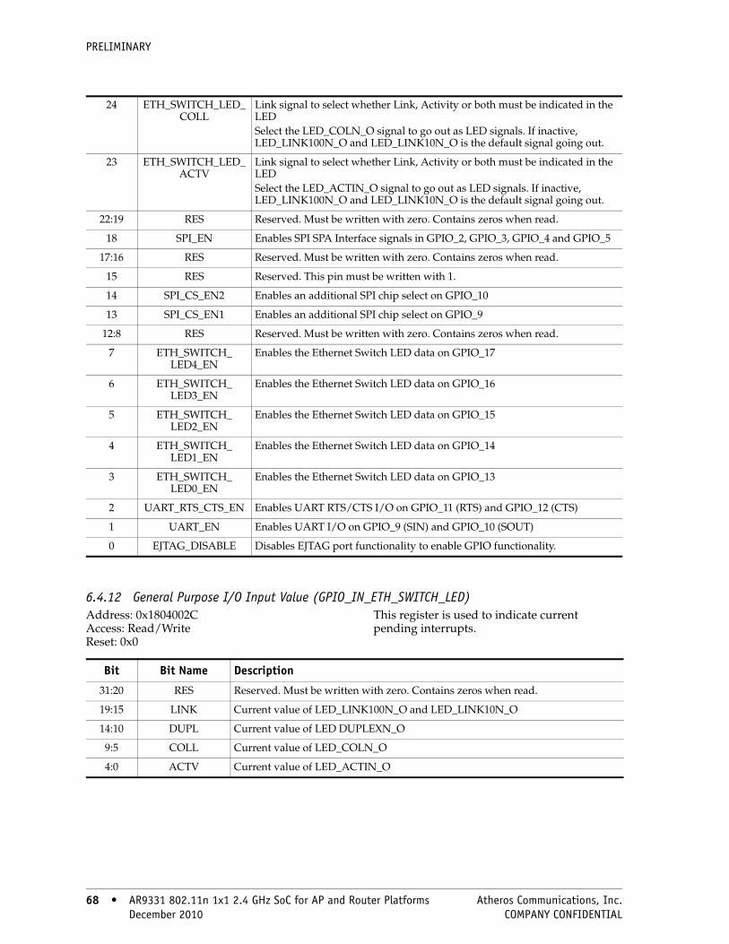
PRELIMINARY
6.4.12 General Purpose I/O Input Value (GPIO_IN_ETH_SWITCH_LED)Address: 0x1804002C Access: Read/Write Reset: 0x0
This register is used to indicate current pending interrupts.
24 ETH_SWITCH_LED_COLL
Link signal to select whether Link, Activity or both must be indicated in the LEDSelect the LED_COLN_O signal to go out as LED signals. If inactive, LED_LINK100N_O and LED_LINK10N_O is the default signal going out.
23 ETH_SWITCH_LED_ACTV
Link signal to select whether Link, Activity or both must be indicated in the LEDSelect the LED_ACTIN_O signal to go out as LED signals. If inactive, LED_LINK100N_O and LED_LINK10N_O is the default signal going out.
22:19 RES Reserved. Must be written with zero. Contains zeros when read.
18 SPI_EN Enables SPI SPA Interface signals in GPIO_2, GPIO_3, GPIO_4 and GPIO_5
17:16 RES Reserved. Must be written with zero. Contains zeros when read.
15 RES Reserved. This pin must be written with 1.
14 SPI_CS_EN2 Enables an additional SPI chip select on GPIO_10
13 SPI_CS_EN1 Enables an additional SPI chip select on GPIO_9
12:8 RES Reserved. Must be written with zero. Contains zeros when read.
7 ETH_SWITCH_ LED4_EN
Enables the Ethernet Switch LED data on GPIO_17
6 ETH_SWITCH_ LED3_EN
Enables the Ethernet Switch LED data on GPIO_16
5 ETH_SWITCH_ LED2_EN
Enables the Ethernet Switch LED data on GPIO_15
4 ETH_SWITCH_ LED1_EN
Enables the Ethernet Switch LED data on GPIO_14
3 ETH_SWITCH_ LED0_EN
Enables the Ethernet Switch LED data on GPIO_13
2 UART_RTS_CTS_EN Enables UART RTS/CTS I/O on GPIO_11 (RTS) and GPIO_12 (CTS)
1 UART_EN Enables UART I/O on GPIO_9 (SIN) and GPIO_10 (SOUT)
0 EJTAG_DISABLE Disables EJTAG port functionality to enable GPIO functionality.
Bit Bit Name Description
31:20 RES Reserved. Must be written with zero. Contains zeros when read.
19:15 LINK Current value of LED_LINK100N_O and LED_LINK10N_O
14:10 DUPL Current value of LED DUPLEXN_O
9:5 COLL Current value of LED_COLN_O
4:0 ACTV Current value of LED_ACTIN_O
68 • AR9331 802.11n 1x1 2.4 GHz SoC for AP and Router Platforms Atheros Communications, Inc. 68 • December 2010 COMPANY CONFIDENTIAL

PRELIMINARY
6.4.13 Extended GPIO Function Control (GPIO_FUNCTION_2)Address: 0x18040030 Access: Read/Write Reset: 0x0
This register is used to indicate current pending interrupts.
Bit Bit Name Description
31:20 RES Reserved. Must be written with zero. Contains zeros when read.
18:16 MDIO_SLV_PHY_ADR Sets the PHY address for MDIO slave functions
15:13 RES Reserved. Must be written with zero. Contains zeros when read.
12 XLNA_EN Enables control to the external LNA on GPIO28
11 WLAN_LED2_ EN Enables the second WLAN LED function on GPIO1
10 WLAN_LED1_ EN Enables the first WLAN LED function on GPIO0
9 JUMPSTART_ DISABLE Disables Jumpstart input function on GPIO11
8 WPS_DISABLE Disables the WPS input function on GPIO12
7:6 RES Reserved. Must be written with zero. Contains zeros when read.
5 I2SD_ON_12 Enables I2S_SD output signal on GPIO_12
4 EN_I2SWS_ON_0 Enables I2S_WS on GPIO_0
3 EN_I2SCK_ON_1 Enables I2S_CK Out on GPIO_1
2 SPDIF_ON23 Enables the SPDIF output on GPIO23
1 I2S_ON_LED Brings out I2S related signals on pins GPIO_14, GPIO_15 and GPIO_16
0 DIS_MIC Disables MIC
Atheros Communications, Inc. AR9331 802.11n 1x1 2.4 GHz SoC for AP and Router Platforms • 69 COMPANY CONFIDENTIAL December 2010 • 69

PRELIMINARY
6.5 PLL Control RegistersTable 6-7 summarizes the AR9331 PLL control registers.
6.5.1 CPU Phase Lock Loop Configuration (CPU_PLL_CONFIG)Address: 0x18050000 Access: Read/Write Reset: See field description
.
6.5.2 CPU Phase Lock Loop Configuration Register 2 (CPU_PLL_CONFIG2)Address: 0x18050004 Access: Read / Write Reset: See field description
Table 6-7. PLL Control Registers Summary
Address Name Description Page0x18050000 CPU_PLL_CONFIG CPU Phase Lock Loop Configuration page 700x18050004 CPU_PLL_CONFIG2 CPU Phase Lock Loop Configuration 2 page 700x18050008 CPU_CLOCK_CONTROL CPU Clock Control page 710x18050010 PLL_DITHER_FRAC CPU PLL Dither FRAC page 710x18050014 PLL_DITHER CPU PLL Dither page 720x18050024 ETHSW_CLOCK_CONTROL Ethernet Switch Clock Control page 720x1805002C ETH_XMII_CONTROL Ethernet XMII Control page 730x18050040 SUSPEND USB Suspend page 730x18050044 WLAN_CLOCK_CONTROL WLAN Clock Control page 74
Bit Bit Name Type Reset Description31 UPDATING R 0x0 This bit is set during the PLL update process. After the software
configures CPU PLL, it takes about 32 µsec for the update to be finished. Software may poll this bit to see if the update has completed.
0 PLL update is complete1 PLL update is pending
30 CPU_PLLPWD RW 0x1 Power down control for CPU PLL29:26 SPARE RW 0x0 Spare registers25:23 OUTDIV RW 0x1 Define the ratio between VCO output and PLL output.
VCOOUT * (1/2(OUTDIV)) = PLLOUT22 RES R 0x0 Reserved. Must be written with zero. Contains zeros when read.21 RANGE RW 0x0 Determines the VCO frequency range of the CPU PLL
20:16 REFDIV RW 0x1 Reference clock divider15:10 DIV_INT RW 0x14 The integer part of the DIV to CPU PLL9:0 RES R 0x0 Reserved. Must be written with zero. Contains zeros when read.
Bit Bit Name Type Reset Description31:12 RES RO 0x0 Reserved. Must be written with zero. Contains zeros when read.11:0 SETTLE_TIME RW 0x550 CPU PLL selling time after power up. The default number is
based on the 40 MHz reference clock cycle.25 ns * 0x550 = 34000 (ns)
70 • AR9331 802.11n 1x1 2.4 GHz SoC for AP and Router Platforms Atheros Communications, Inc. 70 • December 2010 COMPANY CONFIDENTIAL

PRELIMINARY
6.5.3 CPU Clock Control Register (CLOCK_CONTROL)Address: 0x18050008 Access: Read/Write Reset: See field description
Sets and resets the clock switch.
6.5.4 CPU PLL Dither FRAC Register (PLL_DITHER_FRAC)Address: 0x18050010 Access: See field description Reset: See field description
.
Bit Bit Name Type Reset Description
31:20 SPARE RW 0x0 Spare registers
19:17 RES R 0x0 Reserved. Must be written with zero. Contains zeros when read.
16:15 AHB_POST_DIV
RW 0x0 Division ratio for PLL output clock/AHB clock
00 Ratio is 1
01 Ratio is 2
10 Ratio is 3
11 Ratio is 4
14:12 RES R 0x0 Reserved. Must be written with zero. Contains zeros when read.
11:10 DDR_POST_DIV
RW 0x0 Division ratio for PLL output clock/DDR clock
00 Ratio is 1
01 Ratio is 2
10 Ratio is 3
11 Ratio is 4
9:7 RES R 0x0 Reserved. Must be written with zero. Contains zeros when read.
6:5 CPU_POST_DIV
RW 0x0 Division ratio for PLL output clock/CPU clock
00 Ratio is 1
01 Ratio is 2
10 Ratio is 3
11 Ratio is 4
4:3 RES R 0x0 Reserved. Must be written with zero. Contains zeros when read.
2 BYPASS RW 0x1 Bypass PLL. This defaults to 1 for test purposes. Software must enable the CPU PLL for normal operation and then set this bit to 0.
1:0 RES R 0x0 Reserved. Must be written with zero. Contains zeros when read.
Bit Bit Name Type Reset Description
31:30 RES R 0x0 Reserved. Must be written with zero. Contains zeros when read.
29:20 NFRAC_STEP RW 0x1 Step value increased if the DITHER_EN in the CPU PLL DITHER Register is set to 1.
13:10 NFRAC_MIN RW 0x19 NFRAC minimum value. If the DITHER_EN in the CPU PLL DITHER Register is set to 0, the minimum value is used.
9:0 NFRAC_MAX RW 0x3E8 NFRAC maximum value
Atheros Communications, Inc. AR9331 802.11n 1x1 2.4 GHz SoC for AP and Router Platforms • 71 COMPANY CONFIDENTIAL December 2010 • 71

PRELIMINARY
6.5.5 CPU PLL Dither Register (PLL_DITHER)Address: 0x18050014 Access: Read/Write Reset: See field description
Sets the Dither settings of the NFRAC.
6.5.6 Ethernet Switch Clock Control Register (ETHSW_CLOCK CONTROL)Address: 0x18050024 Access: Read/Write Reset: See field description
Sets the Ethernet Switch core.
Bit Bit Name Type Reset Description
31 DITHER_EN RW 0x0 Enables the CPU PLL DITHER function. The Step Value (NFRAC_STEP in the “CPU PLL Dither FRAC Register (PLL_DITHER_FRAC)”) is used to increment every refresh period.
30:14 RES R 0x0 Reserved. Must be written with zero. Contains zeros when read.
13:0 UPDATE_CNT RW 0x3C The number of CPU clocks between two updates in the NFRAC
Bit Bit Name Type Reset Description
31:5 SPARE RW 0x0 Spare registers
4 ENABLE_ETHSW_ CORE_BIAS
RW 0x1 Enables the control register for the Ethernet Switch core bias. The default is enabled.
3 ETHSW_CORE_PLL_PWD
RW 0x1 Power down control register for the Ethernet Switch core internal PLL. The default is power down.
2:0 RES R 0x0 Reserved. Must be written with zero. Contains zeros when read.
72 • AR9331 802.11n 1x1 2.4 GHz SoC for AP and Router Platforms Atheros Communications, Inc. 72 • December 2010 COMPANY CONFIDENTIAL

PRELIMINARY
6.5.7 Ethernet XMII Control Register (ETH_XMII_CONTROL)Address: 0x1805002C Access: Read/Write Reset: See field description
Sets and resets the clock switch.
6.5.8 Suspend Register (SUSPEND)
Address: 0x18050040 Access: Read/Write Reset See field description
This register is used to set the USB suspends for the reference clock.
Bit Bit Name Type Reset Description
31 TX_INVERT RW 0x0 Decides to select the inversion of the XMII TX clock or not
30 GIGE_QUAD RW 0x0 Clock speed selection for the external XMII TX clock
0 25 MHz
1 125 MHz
29:28 RX_DELAY RW 0x0 Used to select the different delay values for the external XMII RX clock
27:26 TX_DELAY RW 0x0 Used to select the different delay values for the external XMII TX clock
25 XMII_GIGE RW 0x0 Speed selection for PHY mode
0 10/100 Mbps PHY mode
1 1 Gbps PHY mode
24 OFFSET_PHASE RW 0x0 Used to select the Phase count to generate the XMII clock
0 Select PHASE0_CNT for generating the XMII clock
1 Select PHASE1_CNT for generating the XMII clock
23:16 OFFSET_CNT RW 0x0 The offset to start the count for generating the XMII clock
15:8 PHASE1_CNT RW 0x1 The second selection of the divisor for generating the XMII clock
7:0 PHASE0_CNT RW 0x1 The first selection of the divisor for generating the XMII clock
Bit Bit Name Type Reset Description
31:28 RES RO 0x0 Reserved. Must be written with zero. Contains zeros when read.
27.8 RESTART_TIME RW 0x550 Number for REFCLK cycles to hold off REFCLK output to the digital clock module after crystal has been powered on after a USB Suspend.
7:1 RES RO 0x0 Reserved. Must be written with zero. Contains zeros when read.
0 ENABLE RW 0x0 Setting this bit will turn off the REFCLK and assert the power down signal to crystal during USB suspend. This bit should be cleared during USB resume.
Atheros Communications, Inc. AR9331 802.11n 1x1 2.4 GHz SoC for AP and Router Platforms • 73 COMPANY CONFIDENTIAL December 2010 • 73

PRELIMINARY
6.5.9 WLAN Clock Control Register (WLAN_CLOCK_CONTROL)Address: 0x18050044 Access: Read/Write Reset: See field description
This register is used to indicate the parts of the divider.
Bit Bit Name Type Reset Description31:13 RES RO 0x0 Reserved. Must be written with zero. Contains zeros when read.
12 UART_CLK88 RW 0x0 Software-controlled UART clock
0 Reference Clock
1 88 MHz
11 RES RO 0x0 Reserved. Must be written with zero. Contains zeros when read.
10 RADIO_ COLD_RST_
CTL
RW 0x0 Software-controlled cold reset to radio module
0 Controlled by the USB Suspend mechanism
1 Assert reset
9 CLKGEN_ COLD_RST_
CTL
RW 0x0 Software-controlled cold reset to clock generation module
0 Controlled by the USB suspend mechanism
1 Assert reset
8 WLANRST_ CTL_MASK
RW 0x0 Reset control mask for the clock generation module and radio
0 Controlled by CLK_GEN_COLD_RST_CTL and RADIO_COLD_RST_CTL
1 Reset controlled by WLAN RTC
7:5 RES RO 0x0 Reserved. Must be written with zero. Contains zeros when read.
4 GLBL_CLK_ EN
RW 0x0 If the CLK_CTL_MASK is set to 0, this bit is used to control the WLAN main clocks from the radio
0 Enables the WLAN main clocks from the radio module
1 Allow the WLAN RTC to control the WLAN main clocks from the radio module
3 WLAN_PLL_PWD_CTL
RW 0x1 If the CLK_CTL_MASK is set to 0, this bit is used to control the power-down of the WLAN_PLL
0 Allow the USB Suspend mechanism to control the power-down of the WLAN PLL
1 Allow the WLAN RTC or USB Suspend mechanism to control the power-down of the WLAN PLL
2 CLKIN_CTL RW 0x0 If the CLK_CTL_MASK is set to 0, this bit is used to control the power-down of the global reference clock
0 Allow the USB Suspend mechanism to control the gating for the REFCLK
1 Allow the WLAN RTC or USB Suspend mechanism to control the gating of the REFCLK
1 PWDN_CTL RW 0x0 If the CLK_CTL_MASK is set to 0, this bit is used to control the power-down of the crystal pad
0 Crystal pad is enabled
1 Allow the USB Suspend mechanism to control the power down of the crystal pad
0 CLK_CTL_ MASK
RW 0x0 The control mask for the crystal pad, reference clock, WLAN PLL and WLAN main clocks, from the radio
0 Controlled by the PWDN_CTL, CLKIN_CTL, WLAN_PLL_PWD_CTL and GLBL_CLK_EN, individually
1 Controlled only by the WLAN RTC
74 • AR9331 802.11n 1x1 2.4 GHz SoC for AP and Router Platforms Atheros Communications, Inc. 74 • December 2010 COMPANY CONFIDENTIAL
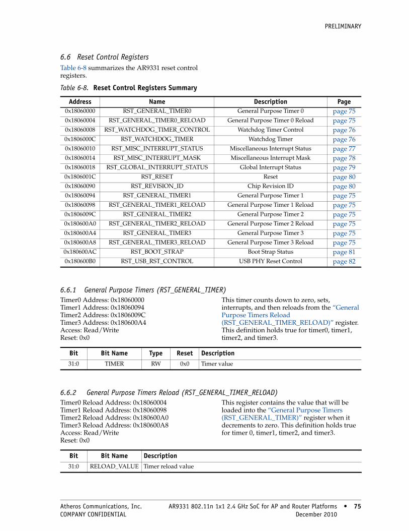
PRELIMINARY
6.6 Reset Control RegistersTable 6-8 summarizes the AR9331 reset control registers.
6.6.1 General Purpose Timers (RST_GENERAL_TIMER)Timer0 Address: 0x18060000 Timer1 Address: 0x18060094 Timer2 Address: 0x1806009C Timer3 Address: 0x180600A4 Access: Read/Write Reset: 0x0
This timer counts down to zero, sets, interrupts, and then reloads from the “General Purpose Timers Reload (RST_GENERAL_TIMER_RELOAD)” register. This definition holds true for timer0, timer1, timer2, and timer3.
6.6.2 General Purpose Timers Reload (RST_GENERAL_TIMER_RELOAD)Timer0 Reload Address: 0x18060004 Timer1 Reload Address: 0x18060098 Timer2 Reload Address: 0x180600A0 Timer3 Reload Address: 0x180600A8 Access: Read/Write Reset: 0x0
This register contains the value that will be loaded into the “General Purpose Timers (RST_GENERAL_TIMER)” register when it decrements to zero. This definition holds true for timer 0, timer1, timer2, and timer3.
Table 6-8. Reset Control Registers Summary
Address Name Description Page0x18060000 RST_GENERAL_TIMER0 General Purpose Timer 0 page 750x18060004 RST_GENERAL_TIMER0_RELOAD General Purpose Timer 0 Reload page 750x18060008 RST_WATCHDOG_TIMER_CONTROL Watchdog Timer Control page 760x1806000C RST_WATCHDOG_TIMER Watchdog Timer page 760x18060010 RST_MISC_INTERRUPT_STATUS Miscellaneous Interrupt Status page 770x18060014 RST_MISC_INTERRUPT_MASK Miscellaneous Interrupt Mask page 780x18060018 RST_GLOBAL_INTERRUPT_STATUS Global Interrupt Status page 790x1806001C RST_RESET Reset page 800x18060090 RST_REVISION_ID Chip Revision ID page 800x18060094 RST_GENERAL_TIMER1 General Purpose Timer 1 page 750x18060098 RST_GENERAL_TIMER1_RELOAD General Purpose Timer 1 Reload page 750x1806009C RST_GENERAL_TIMER2 General Purpose Timer 2 page 750x180600A0 RST_GENERAL_TIMER2_RELOAD General Purpose Timer 2 Reload page 750x180600A4 RST_GENERAL_TIMER3 General Purpose Timer 3 page 750x180600A8 RST_GENERAL_TIMER3_RELOAD General Purpose Timer 3 Reload page 750x180600AC RST_BOOT_STRAP Boot Strap Status page 810x180600B0 RST_USB_RST_CONTROL USB PHY Reset Control page 82
Bit Bit Name Type Reset Description31:0 TIMER RW 0x0 Timer value
Bit Bit Name Description31:0 RELOAD_VALUE Timer reload value
Atheros Communications, Inc. AR9331 802.11n 1x1 2.4 GHz SoC for AP and Router Platforms • 75 COMPANY CONFIDENTIAL December 2010 • 75

PRELIMINARY
6.6.3 Watchdog Timer Control Register (RST_WATCHDOG_TIMER_CONTROL)Address: 0x18060008 Access: See field description Reset: 0x0
Sets the action to take when the watchdog timer reaches zero. The options are reset, non-maskable interrupt and general purpose interrupt after reaching zero.
6.6.4 Watchdog Timer Register (RST_WATCHDOG_TIMER)Address: 0x1806000C Access: Read/Write Reset: 0x0
Specifies the action for the watchdog timer control to take when this watchdog timer reaches zero.
Bit Bit Name Type Description
31 LAST RO Indicates if the last reset was due to a watchdog timeout
30:2 RES RO Reserved. Must be written with zero. Contains zeros when read.
1:0 ACTION RW The action to be taken after the timer reaches zero
00 No action
01 General purpose interrupt
10 Non-maskable interrupt
11 Full chip reset
Bit Bit Name Description
31:0 TIMER Counts down to zero and stays at zero until the software sets this timer to another value. These bits should be set to a non-zero value before updating the “Watchdog Timer Control Register (RST_WATCHDOG_TIMER_CONTROL)” register to a non-zero number.
76 • AR9331 802.11n 1x1 2.4 GHz SoC for AP and Router Platforms Atheros Communications, Inc. 76 • December 2010 COMPANY CONFIDENTIAL

PRELIMINARY
6.6.5 Miscellaneous Interrupt Status (RST_MISC_INTERRUPT_STATUS)Address: 0x18060010 Access: Read-Write to Clear Reset: 0x0
Sets the current state of the interrupt lines that are combined to form the MiscInterupt to the processor. All bits of this register need a write to clear.
Bit Bit Name Description
31:17 RES Reserved. Must be written with zero. Contains zeros when read.
16 DDR_ACTIVITY_ IN_SF
The interrupt generated when there is access activity to the DDR during self-refreshing mode from any AMBA host
15 DDR_SF_EXIT The interrupt generated when the DDR leaves self-refreshing mode
14 DDR_SF_ENTRY The interrupt generated when the DDR enters self-refreshing mode
13 MDIO_SLAVE_ INT
The interrupt generated by the MDIO slave control
12 ETHSW_MAC_INT The interrupt generated by the Ethernet Switch
11 RES Reserved. Must be written with zero. Contains zeros when read.
10 TIMER3_INT The interrupt corresponding to General Purpose Timer3. This bit is cleared after being read. The timer has been immediately reloaded from the “General Purpose Timers Reload (RST_GENERAL_TIMER_RELOAD)” register.
9 TIMER2_INT The interrupt corresponding to General Purpose Timer2. This bit has been cleared after being read. The timer will be immediately reloaded from the “General Purpose Timers Reload (RST_GENERAL_TIMER_RELOAD)” register.
8 TIMER1_INT The interrupt corresponding to General Purpose Timer1. This bit has been cleared after being read. The timer will be immediately reloaded from the “General Purpose Timers Reload (RST_GENERAL_TIMER_RELOAD)” register.
7:5 RES Reserved. Must be written with zero. Contains zeros when read.
4 WATCHDOG_ INT The Watchdog Timer interrupt. This interrupt is generated when the Watchdog Timer reaches zero and the Watchdog Configuration register is configured to generate a general-purpose interrupt.
3 UART_INT The UART interrupt. UART interrupt registers must be read before this interrupt can be cleared.
2 GPIO_INT The GPIO interrupt. Individual lines must be masked before this interrupt can be cleared.
1 ERROR_INT An interrupt caused by an error on the internal PIO bus. Error logic registers must be read and cleared before this interrupt can be cleared.
0 TIMER_INT Interrupt occurring in correspondence to the general purpose timer0. This bit is cleared after being read. The timer has already been reloaded from the “General Purpose Timers Reload (RST_GENERAL_TIMER_RELOAD)” register.
Atheros Communications, Inc. AR9331 802.11n 1x1 2.4 GHz SoC for AP and Router Platforms • 77 COMPANY CONFIDENTIAL December 2010 • 77
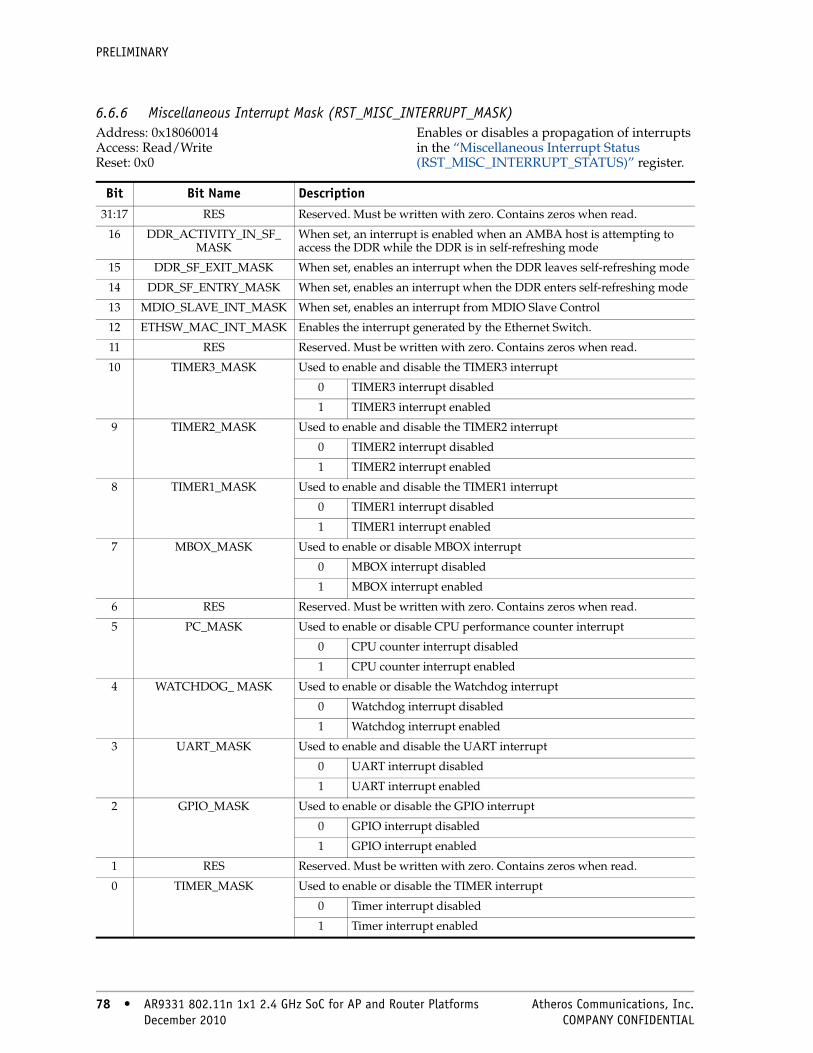
PRELIMINARY
6.6.6 Miscellaneous Interrupt Mask (RST_MISC_INTERRUPT_MASK)Address: 0x18060014 Access: Read/Write Reset: 0x0
Enables or disables a propagation of interrupts in the “Miscellaneous Interrupt Status (RST_MISC_INTERRUPT_STATUS)” register.
Bit Bit Name Description31:17 RES Reserved. Must be written with zero. Contains zeros when read.
16 DDR_ACTIVITY_IN_SF_ MASK
When set, an interrupt is enabled when an AMBA host is attempting to access the DDR while the DDR is in self-refreshing mode
15 DDR_SF_EXIT_MASK When set, enables an interrupt when the DDR leaves self-refreshing mode
14 DDR_SF_ENTRY_MASK When set, enables an interrupt when the DDR enters self-refreshing mode
13 MDIO_SLAVE_INT_MASK When set, enables an interrupt from MDIO Slave Control
12 ETHSW_MAC_INT_MASK Enables the interrupt generated by the Ethernet Switch.
11 RES Reserved. Must be written with zero. Contains zeros when read.
10 TIMER3_MASK Used to enable and disable the TIMER3 interrupt
0 TIMER3 interrupt disabled
1 TIMER3 interrupt enabled
9 TIMER2_MASK Used to enable and disable the TIMER2 interrupt
0 TIMER2 interrupt disabled
1 TIMER2 interrupt enabled
8 TIMER1_MASK Used to enable and disable the TIMER1 interrupt
0 TIMER1 interrupt disabled
1 TIMER1 interrupt enabled
7 MBOX_MASK Used to enable or disable MBOX interrupt
0 MBOX interrupt disabled
1 MBOX interrupt enabled
6 RES Reserved. Must be written with zero. Contains zeros when read.
5 PC_MASK Used to enable or disable CPU performance counter interrupt
0 CPU counter interrupt disabled
1 CPU counter interrupt enabled
4 WATCHDOG_ MASK Used to enable or disable the Watchdog interrupt
0 Watchdog interrupt disabled
1 Watchdog interrupt enabled
3 UART_MASK Used to enable and disable the UART interrupt
0 UART interrupt disabled
1 UART interrupt enabled
2 GPIO_MASK Used to enable or disable the GPIO interrupt
0 GPIO interrupt disabled
1 GPIO interrupt enabled
1 RES Reserved. Must be written with zero. Contains zeros when read.
0 TIMER_MASK Used to enable or disable the TIMER interrupt
0 Timer interrupt disabled
1 Timer interrupt enabled
78 • AR9331 802.11n 1x1 2.4 GHz SoC for AP and Router Platforms Atheros Communications, Inc. 78 • December 2010 COMPANY CONFIDENTIAL

PRELIMINARY
6.6.7 Global Interrupt Status (RST_GLOBAL_INTERRUPT_STATUS)Address: 0x18060018 Access: Read-Only Reset: 0x0
This register reflects the CPU 6-bit interrupt input.
Bit Bit Name Description
31:6 RES Reserved. Must be written with zero. Contains zeros when read.
6 AMBA_INT WLAN MAC interrupt
5 TIMER_INT Internal count/compare timer interrupt; cleared after read.
4 MISC_INT Miscellaneous interrupt. This bit is cleared after being read. Source of the interrupt is available on the “Miscellaneous Interrupt Status (RST_MISC_INTERRUPT_STATUS)” register.
3 GE1_INT Ethernet1 interrupt. This bit is cleared after read. Information available in the Ethernet1 register space.
2 GE0_INT Ethernet 0 interrupt. This bit is cleared after read. Information available in the Ethernet0 register space.
1 USB_INT USB interrupt. This bit is cleared after read.
0 RES Reserved. Must be written with zero. Contains zeros when read.
Atheros Communications, Inc. AR9331 802.11n 1x1 2.4 GHz SoC for AP and Router Platforms • 79 COMPANY CONFIDENTIAL December 2010 • 79
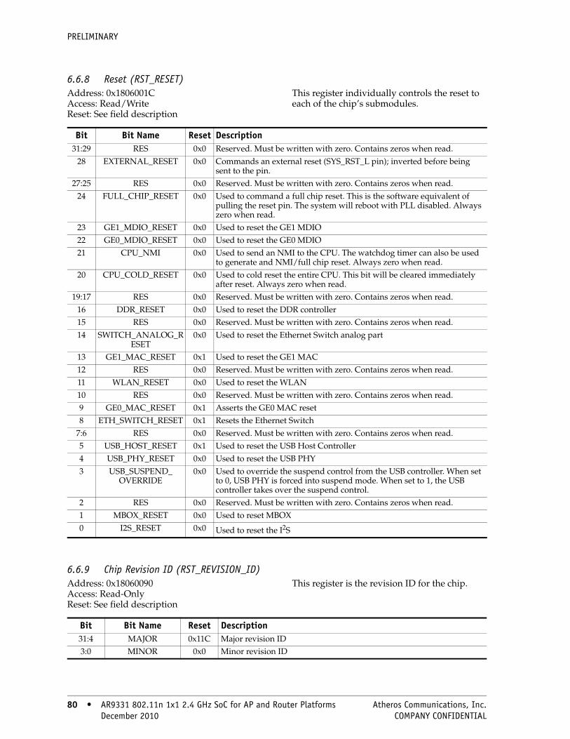
PRELIMINARY
6.6.8 Reset (RST_RESET)Address: 0x1806001C Access: Read/Write Reset: See field description
This register individually controls the reset to each of the chip’s submodules.
6.6.9 Chip Revision ID (RST_REVISION_ID)Address: 0x18060090 Access: Read-Only Reset: See field description
This register is the revision ID for the chip.
Bit Bit Name Reset Description31:29 RES 0x0 Reserved. Must be written with zero. Contains zeros when read.
28 EXTERNAL_RESET 0x0 Commands an external reset (SYS_RST_L pin); inverted before being sent to the pin.
27:25 RES 0x0 Reserved. Must be written with zero. Contains zeros when read.
24 FULL_CHIP_RESET 0x0 Used to command a full chip reset. This is the software equivalent of pulling the reset pin. The system will reboot with PLL disabled. Always zero when read.
23 GE1_MDIO_RESET 0x0 Used to reset the GE1 MDIO
22 GE0_MDIO_RESET 0x0 Used to reset the GE0 MDIO21 CPU_NMI 0x0 Used to send an NMI to the CPU. The watchdog timer can also be used
to generate and NMI/full chip reset. Always zero when read.
20 CPU_COLD_RESET 0x0 Used to cold reset the entire CPU. This bit will be cleared immediately after reset. Always zero when read.
19:17 RES 0x0 Reserved. Must be written with zero. Contains zeros when read.
16 DDR_RESET 0x0 Used to reset the DDR controller15 RES 0x0 Reserved. Must be written with zero. Contains zeros when read.
14 SWITCH_ANALOG_RESET
0x0 Used to reset the Ethernet Switch analog part
13 GE1_MAC_RESET 0x1 Used to reset the GE1 MAC
12 RES 0x0 Reserved. Must be written with zero. Contains zeros when read.
11 WLAN_RESET 0x0 Used to reset the WLAN
10 RES 0x0 Reserved. Must be written with zero. Contains zeros when read.9 GE0_MAC_RESET 0x1 Asserts the GE0 MAC reset
8 ETH_SWITCH_RESET 0x1 Resets the Ethernet Switch
7:6 RES 0x0 Reserved. Must be written with zero. Contains zeros when read.5 USB_HOST_RESET 0x1 Used to reset the USB Host Controller
4 USB_PHY_RESET 0x0 Used to reset the USB PHY
3 USB_SUSPEND_ OVERRIDE
0x0 Used to override the suspend control from the USB controller. When set to 0, USB PHY is forced into suspend mode. When set to 1, the USB controller takes over the suspend control.
2 RES 0x0 Reserved. Must be written with zero. Contains zeros when read.1 MBOX_RESET 0x0 Used to reset MBOX
0 I2S_RESET 0x0 Used to reset the I2S
Bit Bit Name Reset Description31:4 MAJOR 0x11C Major revision ID3:0 MINOR 0x0 Minor revision ID
80 • AR9331 802.11n 1x1 2.4 GHz SoC for AP and Router Platforms Atheros Communications, Inc. 80 • December 2010 COMPANY CONFIDENTIAL

PRELIMINARY
6.6.10 Bootstrap Status (BOOT_STRAP)Address: 0x180600AC Access: Read/Write Reset: See field description
This register denotes the bootstrap status and detection.
Bit Bit Name Reset Description
31:19 RES 0x0 Reserved. Must be written with zero. Contains zeros when read.
18 MDIO_GPIO_EN 0x0 Enables the MDC and MDIO function on GPIO26 and GPIO28
17 MDIO_SLAVE_ EN
0x0 MDC, MDIO role selection
0 AR9331 is the master
1 AR9331 is the slave
16 JTAG_APB_SEL 0x0 Selection of the JTAG or AHB interface for the MAC register. For normal operation mode, SW should select the APB interface before register access.
0 APB
1 JTAG
15:14 RES 0x0 Reserved. Must be written with zero. Contains zeros when read.
13:12 MEM_TYPR 0x0 Indicates external memory type; power on detection (GPIO12 and GPIO28)
00 SDRAM
01 DDR1 RAM
10 DDR2 RAM
11:9 RES 0x0 Reserved. Must be written with zero. Contains zeros when read.
8 FW_DOWNLOAD 0x0 Indicates which interface will be used to download firmware. Power on detection on GPIO16.
0 Read from USB interface
1 Read from MDIO interface
7:5 RES 0x0 Reserved. Must be written with zero. Contains zeros when read.
4 EEPBUSY 0x0 MAC, EEPROM or OTP busy indication
3 USB_MODE 0x0 Indicates if the interface is in host mode or device mode. Power on detection is on GPIO13.
0 Device
1 Host
2 JTAG_FOR_ICE 0x0 Indicates if the ICE interface is for General JTAG functions or for CPU ICE. Power on detection is on GPIO11
0 General JTAG
1 CPU ICE
1 BOOT_FROM_SPI 0x0 Indicates if the boot sequence is from the SPI or the internal ROM. Power detection is on GPIO1
0 ROM
1 SPI Flash
0 SEL_25M_40M 0x0 Indicates the frequency of the external clock. Power detection on GPIO0.
0 25M
1 40M
Atheros Communications, Inc. AR9331 802.11n 1x1 2.4 GHz SoC for AP and Router Platforms • 81 COMPANY CONFIDENTIAL December 2010 • 81

PRELIMINARY
6.6.11 USB PHY Reset Control (USB_PHY_RESET)Address: 0x180600B0 Access: Read/Write Reset: See field description
This register is the revision ID for the chip.
Bit Bit Name Reset Description31:4 RES 0x0 Reserved. Must be written with zero. Contains zeros when read.
3 USB_PHY_EXT_ PWR_SEQ
0x0 Power control selection. If set to 1, use bits [2:0] to control the USB PHY. Otherwise, use the controls from the USB controller or suspend hardware.
2 USB_PHY_PLL_ PWD_EXT
0x0 Used to power down the PLL inside the USB PHY if bit [3] is set to 1
1 USB_PHY_ DRESET_N
0x0 Used to reset the digital part of the USB PHY if bit [3] is set to 1
0 USB_PHY_ ARESET_N
0x0 Used to reset the analog part of the USB PHY if bit [3] is set to 1
82 • AR9331 802.11n 1x1 2.4 GHz SoC for AP and Router Platforms Atheros Communications, Inc. 82 • December 2010 COMPANY CONFIDENTIAL

PRELIMINARY
6.7 GMAC RegisterTable 6.7 summarizes the GMAC register for the AR9331.
6.7.1 Ethernet Configuration (ETH_CFG)Address: 0x18070000 Access: Read/Write Reset: 0x0
Table 6-9. GMAC Register Summary
Address Name Description Page0x18070000 ETH_CFG Ethernet Configuration page 83
Bit Bit Name Type Description
31:11 RES RO Reserved. Must be written with zero. Contains zeros when read.
10 CFG_RMII_GE0_ SPEED
RW Selects the RMII speed for GMAC0
0 10 Mb
1 100 Mb
9 CFG_RMII_GE0 RW Selects the RMII mode for GMAC0
8 CFG_SW_PHY_ ADDR_SWAP
RW Exchanges the address of PHY port 0 with that of PHY port 4 in the Ethernet switch
7 CFG_SW_PHY_ SWAP
RW Used to switch the wires connection of PHY port 0 with that of port 4 in the Ethernet switch. MAC1 and PHY4 are paired while MAC5 and PHY0 are paired
6 RES RO Reserved. Must be written with zero. Contains zeros when read.
5 CFG_GE0_ERR_ EN
RW Enables GMAC0’s RX_ERR function in GMII or MII mode
4 CFG_MII_GE0_ SLAVE
RW Set this bit to let GMAC0 be the Tx clock receiver in MII mode
3 CFG_MII_GE0_ MASTER
RW Set this bit to let GMAC0 be the Rx clock provider in MII mode
2 CFG_GMII_GE0 RW GMII mode selection for GMAC0
1 CFG_MII_GE0 RW MII mode selection for GMAC0
0 CFG_RGMII_GE0 RW RGMII mode selection for GMAC0
Atheros Communications, Inc. AR9331 802.11n 1x1 2.4 GHz SoC for AP and Router Platforms • 83 COMPANY CONFIDENTIAL December 2010 • 83

PRELIMINARY
6.8 SLIC RegistersTable 6-10 summarizes the SLIC registers for the AR9331.
6.8.1 SLIC Slots Register (SLIC_SLOT)Address: 0x18090000 Access: Read/Write Reset: See field description
This register indicates the number of slots supported by the connected SLIC device. Current implementation supports 1 to 64 slots, 8 bits each.
6.8.2 SLIC Clock Control Register (SLIC_CLOCK_CONTROL)Address: 0x18090004 Access: Read/Write Reset: 0x0
This register defines the divider value of AUDIO_PLL_CLK. This value depends on the SLIC_SLOT_SEL value.
Table 6-10. SLIC Registers Summary
Address Name Description Page
0x18090000 SLIC_SLOT SLIC Slots Register page 84
0x18090004 SLICK_CLOCK_CONTROL SLIC Clock Control page 84
0x18090008 SLIC_CTRL SLIC Control page 85
0x1809000C SLIC_TX_SLOTS1 SLIC Tx Slots Register page 85
0x18090010 SLIC_TX_SLOTS2 SLIC Tx Slots 2 Register page 85
0x18090014 SLIC_RX_SLOTS1 SLIC Rx Slots Register page 85
0x18090018 SLIC_RX_SLOTS2 SLIC Rx Slots 2 Register page 86
0x1809001C SLIC_TIMING_CTRL SLIC Timing Control Register page 86
0x18090020 SLIC_INTR SLIC Interrupts Register page 86
0x18090024 SLIC_SWAP SLIC Swap Registers page 87
Bit Bit Name Reset Description
31:7 RES 0x0 Reserved. Must be written with zero. Contains zeros when read.
6:0 SEL 0x20 The number of SLIC slots
Bit Bit Name Description
31:6 RES Reserved. Must be written with zero. Contains zeros when read.
5:0 DIV Defines the divider value of AUDIO_PLL_CLK.
84 • AR9331 802.11n 1x1 2.4 GHz SoC for AP and Router Platforms Atheros Communications, Inc. 84 • December 2010 COMPANY CONFIDENTIAL

PRELIMINARY
6.8.3 SLIC Control Register (SLIC_CTRL)Address: 0x18090008 Access: Read/Write Reset: See field description
This register defines the various control signals of the SLIC controller.
6.8.4 SLIC Tx Slots 1 Register (SLIC_TX_SLOTS1)Address: 0x1809000C Access: Read/Write Reset: 0x0
This register defines the LSB 32 Tx slots, one of which is hot encoded.
6.8.5 SLIC Tx Slots 2 Register (SLIC_TX_SLOTS2)Address: 0x18090010 Access: Read/Write Reset: 0x0
This register defines the MSB 32 Tx slots, one of which is hot encoded.
6.8.6 SLIC Rx Slots 1 Register (SLIC_RX_SLOTS1)Address: 0x18090014 Access: Read/Write Reset: 0x0
This register defines the LSB 32 Rx slots, one of which is hot encoded.
Bit Bit Name Reset Description
31:4 RES 0x0 Reserved. Must be written with zero. Contains zeros when read.
3 CLK_EN 0x0 Acts as a clock gate enable. It gates the AUDIO_PLL/external clock.
2 MASTER_SLAVE 0x1 Used to select the mode for SLIC control functionality
0 Slave mode
1 Master mode
1 SLIC_EN 0x0 Enables the total SLIC controller functionality either in master or slave mode
0 SLIC_INTR 0x0 SLIC interrupt
Bit Bit Name Description
31:0 ONEHOT The hot encoded LSB 32 Tx slot
Bit Bit Name Description
31:0 ONEHOT The hot encoded MSB 32 Tx slot
Bit Bit Name Description
31:0 ONEHOT The hot encoded LSB 32 Rx slot
Atheros Communications, Inc. AR9331 802.11n 1x1 2.4 GHz SoC for AP and Router Platforms • 85 COMPANY CONFIDENTIAL December 2010 • 85

PRELIMINARY
6.8.7 SLIC Rx Slots 2 Register (SLIC_RX_SLOTS2)Address: 0x18090018 Access: Read/Write Reset: 0x0
This register defines the MSB 32 Rx slots, one of which is hot encoded.
6.8.8 SLIC Timing Control Register (SLIC_TIMING_CTRL)Address: 0x1809001C Access: Read/Write Reset: See field description
This register sets the timing control related bits for FRAME_SYNC and data.
6.8.9 SLIC Interrupt Register (SLIC_INTR)Address: 0x18090020 Access: Read/Write Reset: See field description
This register is used for the SLIC interrupt and status registers.
Bit Bit Name Description31:0 ONEHOT The hot encoded MSB 32 Rx slot
Bit Bit Name Type Reset Description31:9 RES RO 0x0 Reserved. Must be written with zero. Contains zeros when read.
8:7 RXDATA_ SAMPLE_
POS
RW 0x0 A 0 or 1 denotes the Rx data will be sampled at the first negative edge after a frame sync positive edge.A 2 means the Rx data will be sampled at the first positive edge after a frame sync positive edge.A 3 denotes the Rx data will be sampled at the second negative edge after a frame sync positive edge.
6:5 TXDATA_FS_SYNC
RW 0x1 A 1 or 0 denotes that the Tx data will be sent along with a frame sync positive edge. A 2 means the Tx data will be sent in the next positive edge of the BLT_CLK after a frame sync positive edge.A 3 denotes that the Tx data will be sent along in the next negative edge of the BLT_CLK after a frame sync positive edge
4:2 LONG_ FSCLKS
RW 0x0 This field depends on the LONG_FS. If the LONG_FS = 1, then this field specifies then number of BLT_CLKs for which FS is high. 0 means 1 BLT_CLK, and 7 means 8 BLT_CLKs
1 FS_POS RW 0x1 0 Send FS at the negative edge of the BLT_CLK
1 Send FS at the positive edge of the BLT_CLK
0 LONG_FS RW 0x1 0 FS is high for a half bit clock
1 FS is high for more than 1 BLT_CLK duration
Bit Bit Name Type Reset Description31:10 RES RW 0x0 Reserved. Must be written with zero. Contains zeros when read.
9:5 STATUS RW 0x0 0 No interrupts
1 At a particular bit location means a particular interrupt is asserted
Bit [0] 1 unexpected frame sync received bit
4:0 MASK RW 0x1f 1f enables all interrupts.
Bit [0] 0 intr0 masked
Bit [1] 0 intr1 masked
Bit [2] 0 intr2 masked
Bit [3] 0 intr3 masked
Bit [4] 0 intr4 masked
86 • AR9331 802.11n 1x1 2.4 GHz SoC for AP and Router Platforms Atheros Communications, Inc. 86 • December 2010 COMPANY CONFIDENTIAL
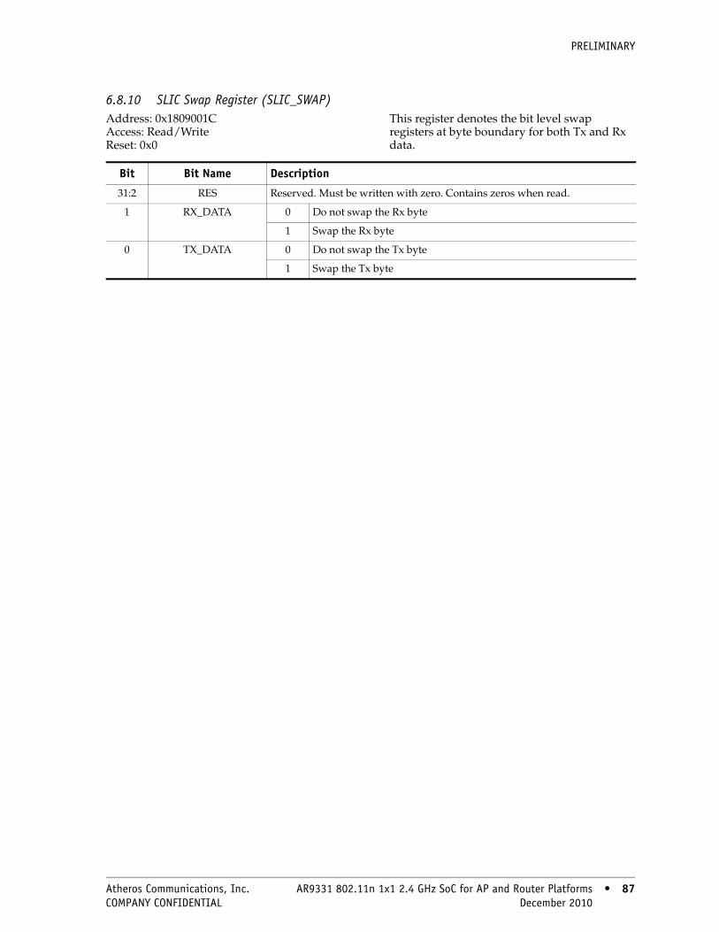
PRELIMINARY
6.8.10 SLIC Swap Register (SLIC_SWAP)Address: 0x1809001C Access: Read/Write Reset: 0x0
This register denotes the bit level swap registers at byte boundary for both Tx and Rx data.
Bit Bit Name Description
31:2 RES Reserved. Must be written with zero. Contains zeros when read.
1 RX_DATA 0 Do not swap the Rx byte
1 Swap the Rx byte
0 TX_DATA 0 Do not swap the Tx byte
1 Swap the Tx byte
Atheros Communications, Inc. AR9331 802.11n 1x1 2.4 GHz SoC for AP and Router Platforms • 87 COMPANY CONFIDENTIAL December 2010 • 87

PRELIMINARY
6.9 MBOX RegistersTable 6-11 summarizes the AR9331 MBOX registers.
6.9.1 Non-Destructive FIFO Status Query (MBOX_FIFO_STATUS)Address: 0x180A0008 Access: Read-Only Reset: 0x0
This register returns the status of the mailbox FIFOs. This register may be read at any time without changing the mailbox state.
Table 6-11. MBOX Local Registers Summary
Address Name Description Page
0x180A0008 MBOX_FIFO_STATUS Non-Destructive FIFO Status Query page 88
0x180A000C SLIC_MBOX_FIFO_STATUS SLIC Non-Destructive FIFO Status Query page 89
0x180A0010 MBOX_DMA_POLICY Mailbox DMA Engine Policy Control page 89
0x180A0014 SLIC_MBOX_DMA_POLICY SLIC Mailbox DMA Engine Policy Control page 90
0x180A0018 MBOX_DMA_RX_ DESCRIPTOR_BASE
Mailbox Rx DMA Descriptors Base Address page 90
0x180A001C MBOX_DMA_RX_CONTROL Mailbox Rx DMA Control page 91
0x180A0020 MBOX_DMA_TX_DESCRIPTOR_ BASE
Mailbox Tx DMA Descriptors Base Address page 91
0x180A0024 MBOX_DMA_TX_CONTROL Mailbox Tx DMA Control page 92
0x180A0028 SLIC_MBOX_DMA_RX_ DESCRIPTOR_BASE
SLIC Mailbox Rx DMA Descriptors Base Address
page 92
0x180A002C SLIC_MBOX_DMA_RX_CONTROL SLIC Mailbox Rx DMA Control page 93
0x180A0030 SLIC_MBOX_DMA_TX_ DESCRIPTOR_ BASE
SLIC Mailbox Tx DMA Descriptors Base Address
page 93
0x180A0034 SLIC_MBOX_DMA_TX_CONTROL SLIC Mailbox Tx DMA Control page 94
0x180A0038 MBOX_FRAME Mailbox FIFO Status page 94
0x180A003C SLIC_MBOX_FRAME SLIC Mailbox FIFO Status page 94
0x180A0040 FIFO_TIMEOUT FIFO Timeout Period page 95
0x180A0044 MBOX_INT_STATUS MBOX Related Interrupt Status page 95
0x180A0048 SLIC_MBOX_INT_STATUS SLIC MBOX Related Interrupt Status page 96
0x180A004C MBOX_INT_ENABLE MBOX Related Interrupt Enables page 96
0x180A0050 SLIC_MBOX_INT_ENABLE SLIC MBOX Related Interrupt Enables page 97
0x180A0058 MBOX_FIFO_RESET MBOX Reset and Clear page 97
0x180A005C SLIC_MBOX_FIFO_RESET SLIC MBOX Reset and Clear page 97
Bit Bit Name Reset Description
31:3 RES 0x0 Reserved. Must be written with zero. Contains zeros when read.
2 EMPTY 0x1 On a read: returns an empty status for the Tx mailbox
1 RES 0x0 Reserved. Must be written with zero. Contains zeros when read.
0 FULL 0x0 On a read: returns a full status for the Rx mailbox
88 • AR9331 802.11n 1x1 2.4 GHz SoC for AP and Router Platforms Atheros Communications, Inc. 88 • December 2010 COMPANY CONFIDENTIAL
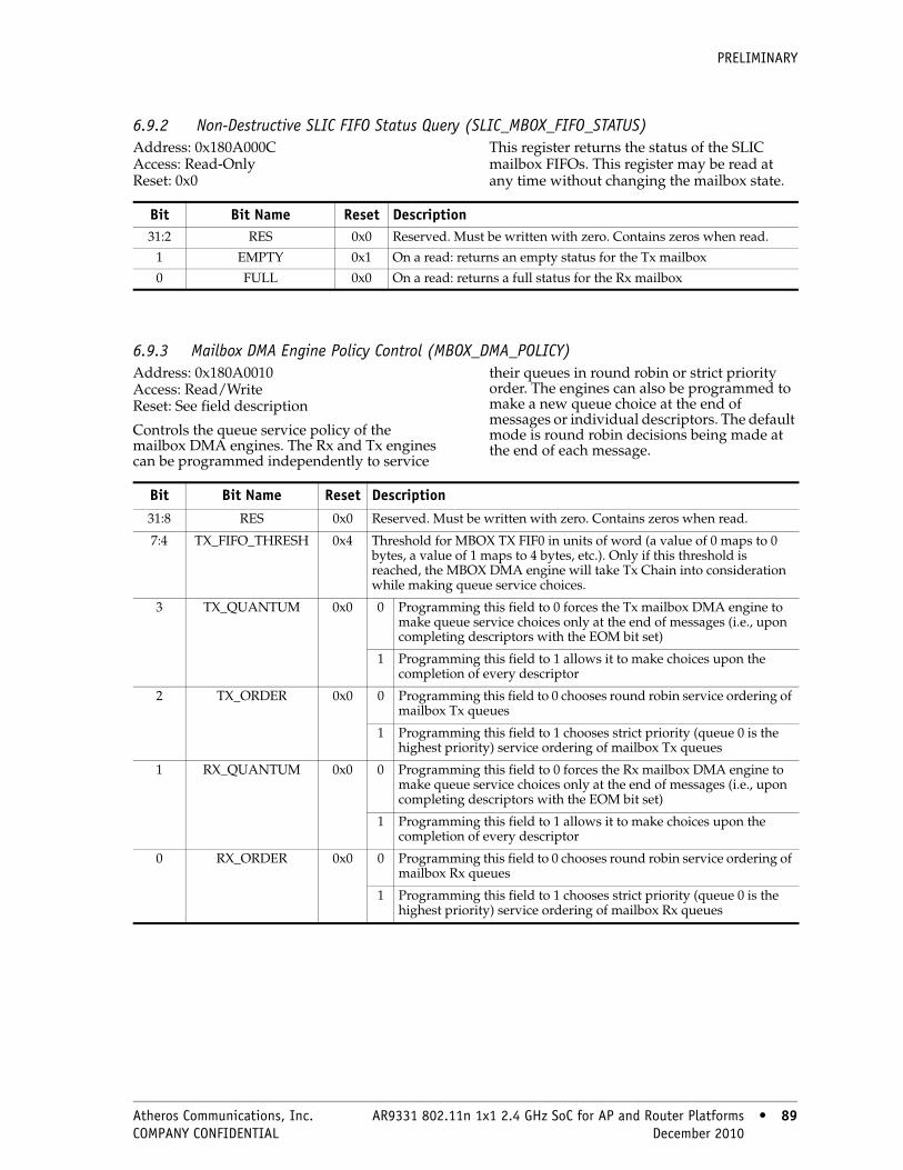
PRELIMINARY
6.9.2 Non-Destructive SLIC FIFO Status Query (SLIC_MBOX_FIFO_STATUS)Address: 0x180A000C Access: Read-Only Reset: 0x0
This register returns the status of the SLIC mailbox FIFOs. This register may be read at any time without changing the mailbox state.
6.9.3 Mailbox DMA Engine Policy Control (MBOX_DMA_POLICY)Address: 0x180A0010 Access: Read/Write Reset: See field description
Controls the queue service policy of the mailbox DMA engines. The Rx and Tx engines can be programmed independently to service
their queues in round robin or strict priority order. The engines can also be programmed to make a new queue choice at the end of messages or individual descriptors. The default mode is round robin decisions being made at the end of each message.
Bit Bit Name Reset Description31:2 RES 0x0 Reserved. Must be written with zero. Contains zeros when read.
1 EMPTY 0x1 On a read: returns an empty status for the Tx mailbox
0 FULL 0x0 On a read: returns a full status for the Rx mailbox
Bit Bit Name Reset Description31:8 RES 0x0 Reserved. Must be written with zero. Contains zeros when read.
7:4 TX_FIFO_THRESH 0x4 Threshold for MBOX TX FIF0 in units of word (a value of 0 maps to 0 bytes, a value of 1 maps to 4 bytes, etc.). Only if this threshold is reached, the MBOX DMA engine will take Tx Chain into consideration while making queue service choices.
3 TX_QUANTUM 0x0 0 Programming this field to 0 forces the Tx mailbox DMA engine to make queue service choices only at the end of messages (i.e., upon completing descriptors with the EOM bit set)
1 Programming this field to 1 allows it to make choices upon the completion of every descriptor
2 TX_ORDER 0x0 0 Programming this field to 0 chooses round robin service ordering of mailbox Tx queues
1 Programming this field to 1 chooses strict priority (queue 0 is the highest priority) service ordering of mailbox Tx queues
1 RX_QUANTUM 0x0 0 Programming this field to 0 forces the Rx mailbox DMA engine to make queue service choices only at the end of messages (i.e., upon completing descriptors with the EOM bit set)
1 Programming this field to 1 allows it to make choices upon the completion of every descriptor
0 RX_ORDER 0x0 0 Programming this field to 0 chooses round robin service ordering of mailbox Rx queues
1 Programming this field to 1 chooses strict priority (queue 0 is the highest priority) service ordering of mailbox Rx queues
Atheros Communications, Inc. AR9331 802.11n 1x1 2.4 GHz SoC for AP and Router Platforms • 89 COMPANY CONFIDENTIAL December 2010 • 89

PRELIMINARY
6.9.4 SLIC Mailbox DMA Engine Policy Control (SLIC_MBOX_DMA_POLICY)Address: 0x180A0014 Access: Read/Write Reset: See field description
Controls the queue service policy of the SLIC mailbox DMA engines. The Rx and Tx engines can be programmed independently to service
their queues in round robin or strict priority order. The engines can also be programmed to make a new queue choice at the end of messages or individual descriptors. The default mode is round robin decisions being made at the end of each message.
6.9.5 Mailbox Rx DMA Descriptors Base Address (MBOX_DMA_RX_DESCRIPTOR_BASE)Address: 0x180A0018 Access: Read/Write Reset: 0x0
Holds the starting address of the descriptor chain for the mailbox’s Rx direction transfers. The DMA engine starts by fetching a descriptor from this address when the START bit in the MBOX_DMA_RX_CONTROL register is set. All DMA descriptors must be 4-byte aligned, so the register’s bottom two bits of the
contents, as well as the bottom two bits of the next descriptor field of the individual descriptors are ignored and assumed to be zeros by the DMA engine. For the purposes of the DMA engine, RX direction is defined to be transfers from the chip to the host interface (nominally, data received from the antenna) and the Tx direction is defined to be transfers from the host interface to the chip (nominally, data to be transmitted to the antenna).
Bit Bit Name Reset Description31:8 RES 0x0 Reserved. Must be written with zero. Contains zeros when read.
7:4 SLIC_TX_FIFO_ THRESH
0x4 Threshold for SLIC MBOX TX FIF0 in units of word (a value of 0 maps to 0 bytes, a value of 1 maps to 4 bytes, etc.). Only if this threshold is reached, the SLIC MBOX DMA engine will take Tx Chain into consideration while making queue service choices
3 TX_QUANTUM 0x0 0 Programming this field to 0 forces the Tx SLIC mailbox DMA engine to make queue service choices only at the end of messages (i.e., upon completing descriptors with the EOM bit set)
1 Programming this field to 1 allows it to make choices upon the completion of every descriptor
2 TX_ORDER 0x0 0 Programming this field to 0 chooses round-robin service ordering of SLIC mailbox Tx queues
1 Programming this field to 1 chooses strict priority (queue 0 is the highest priority) service ordering of mailbox Tx queues
1 RX_QUANTUM 0x0 0 Programming this field to 0 forces the Rx SLIC mailbox DMA engine to make queue service choices only at the end of messages (i.e., upon completing descriptors with the EOM bit set)
1 Programming this field to 1 allows it to make choices upon the completion of every descriptor
0 RX_ORDER 0x0 0 Programming this field to 0 chooses round robin service ordering of SLIC mailbox Rx queues
1 Programming this field to 1 chooses strict priority (queue 0 is the highest priority) service ordering of SLIC mailbox Rx queues
Bit Bit Name Description
31:28 RES Reserved. Must be written with zero. Contains zeros when read.
27:2 ADDRESS Most significant 26 bits of the 4-byte-aligned address of the first descriptor in the DMA chain
1:0 RES Reserved. Must be written with zero. Contains zeros when read.
90 • AR9331 802.11n 1x1 2.4 GHz SoC for AP and Router Platforms Atheros Communications, Inc. 90 • December 2010 COMPANY CONFIDENTIAL
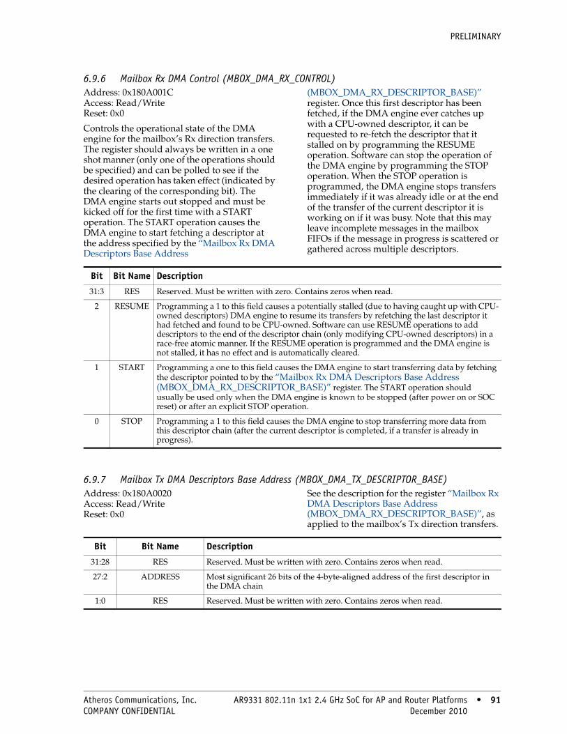
PRELIMINARY
6.9.6 Mailbox Rx DMA Control (MBOX_DMA_RX_CONTROL)Address: 0x180A001C Access: Read/Write Reset: 0x0
Controls the operational state of the DMA engine for the mailbox’s Rx direction transfers. The register should always be written in a one shot manner (only one of the operations should be specified) and can be polled to see if the desired operation has taken effect (indicated by the clearing of the corresponding bit). The DMA engine starts out stopped and must be kicked off for the first time with a START operation. The START operation causes the DMA engine to start fetching a descriptor at the address specified by the “Mailbox Rx DMA Descriptors Base Address
(MBOX_DMA_RX_DESCRIPTOR_BASE)” register. Once this first descriptor has been fetched, if the DMA engine ever catches up with a CPU-owned descriptor, it can be requested to re-fetch the descriptor that it stalled on by programming the RESUME operation. Software can stop the operation of the DMA engine by programming the STOP operation. When the STOP operation is programmed, the DMA engine stops transfers immediately if it was already idle or at the end of the transfer of the current descriptor it is working on if it was busy. Note that this may leave incomplete messages in the mailbox FIFOs if the message in progress is scattered or gathered across multiple descriptors.
6.9.7 Mailbox Tx DMA Descriptors Base Address (MBOX_DMA_TX_DESCRIPTOR_BASE)Address: 0x180A0020 Access: Read/Write Reset: 0x0
See the description for the register “Mailbox Rx DMA Descriptors Base Address (MBOX_DMA_RX_DESCRIPTOR_BASE)”, as applied to the mailbox’s Tx direction transfers.
Bit Bit Name Description
31:3 RES Reserved. Must be written with zero. Contains zeros when read.
2 RESUME Programming a 1 to this field causes a potentially stalled (due to having caught up with CPU-owned descriptors) DMA engine to resume its transfers by refetching the last descriptor it had fetched and found to be CPU-owned. Software can use RESUME operations to add descriptors to the end of the descriptor chain (only modifying CPU-owned descriptors) in a race-free atomic manner. If the RESUME operation is programmed and the DMA engine is not stalled, it has no effect and is automatically cleared.
1 START Programming a one to this field causes the DMA engine to start transferring data by fetching the descriptor pointed to by the “Mailbox Rx DMA Descriptors Base Address (MBOX_DMA_RX_DESCRIPTOR_BASE)” register. The START operation should usually be used only when the DMA engine is known to be stopped (after power on or SOC reset) or after an explicit STOP operation.
0 STOP Programming a 1 to this field causes the DMA engine to stop transferring more data from this descriptor chain (after the current descriptor is completed, if a transfer is already in progress).
Bit Bit Name Description
31:28 RES Reserved. Must be written with zero. Contains zeros when read.
27:2 ADDRESS Most significant 26 bits of the 4-byte-aligned address of the first descriptor in the DMA chain
1:0 RES Reserved. Must be written with zero. Contains zeros when read.
Atheros Communications, Inc. AR9331 802.11n 1x1 2.4 GHz SoC for AP and Router Platforms • 91 COMPANY CONFIDENTIAL December 2010 • 91

PRELIMINARY
6.9.8 Mailbox Tx DMA Control (MBOX_DMA_TX_CONTROL)Address: 0x180A0024 Access: Read/Write Reset: 0x0
See “Mailbox Rx DMA Control (MBOX_DMA_RX_CONTROL)” for description.
6.9.9 SLIC Mailbox Rx DMA Descriptors Base Address (SLIC_MBOX_DMA_RX_DESCRIPTOR_BASE)Address: 0x180A0028 Access: Read/Write Reset: 0x0
Holds the starting address of the descriptor chain for the SLIC mailbox’s Rx direction transfers. The DMA engine starts by fetching a descriptor from this address when the START bit in the “SLIC Mailbox Rx DMA Control (SLIC_MBOX_DMA_RX_CONTROL)” register is set. All DMA descriptors must be 4-byte aligned, so the register’s bottom two bits of the
contents, as well as the bottom two bits of the next descriptor field of the individual descriptors are ignored and assumed to be zeros by the DMA engine. For the purposes of the DMA engine, RX direction is defined to be transfers from the chip to the host interface (nominally, data received from the antenna) and the Tx direction is defined to be transfers from the host interface to the chip (nominally, data to be transmitted to the antenna).
Bit Bit Name Description
31:3 RES Reserved. Must be written with zero. Contains zeros when read.
2 RESUME Programming a one to this field causes a potentially stalled (due to having caught up with CPU-owned descriptors) DMA engine to resume its transfers by refetching the last descriptor it had fetched and found to be CPU-owned. Software can use RESUME operations to keep adding descriptors to the end of the descriptor chain (only modifying CPU-owned descriptors) in a race free atomic manner. If the RESUME operation is programmed and the DMA engine is not stalled, it has no effect and is automatically cleared.
1 START Programming a one to this field causes the DMA engine to start transferring data by fetching the descriptor pointed to by the “Mailbox Tx DMA Descriptors Base Address (MBOX_DMA_TX_DESCRIPTOR_BASE)” register. The START operation should usually be used only when the DMA engine is known to be stopped (after power on or SOC reset) or after an explicit STOP operation.
0 STOP Programming a one to this field causes the DMA engine to stop transferring any more data from this descriptor chain (after the current descriptor is completed, if a transfer is already in progress).
Bit Bit Name Description
31:28 RES Reserved. Must be written with zero. Contains zeros when read.
27:2 ADDRESS Most significant 26 bits of the 4-byte-aligned address of the first descriptor in the DMA chain
1:0 RES Reserved. Must be written with zero. Contains zeros when read.
92 • AR9331 802.11n 1x1 2.4 GHz SoC for AP and Router Platforms Atheros Communications, Inc. 92 • December 2010 COMPANY CONFIDENTIAL

PRELIMINARY
6.9.10 SLIC Mailbox Rx DMA Control (SLIC_MBOX_DMA_RX_CONTROL)Address: 0x180A002C Access: Read/Write Reset: 0x0
Controls the operational state of the DMA engine for the SLIC mailbox’s Rx direction transfers. The register should always be written in a one shot manner (only one of the operations should be specified) and can be polled to see if the desired operation has taken effect (indicated by the clearing of the corresponding bit). The DMA engine starts out stopped and must be kicked off for the first time with a START operation. The START operation causes the DMA engine to start fetching a descriptor at the address specified by the “SLIC Mailbox Rx DMA Descriptors Base Address
(SLIC_MBOX_DMA_RX_DESCRIPTOR_BASE)” register. Once this first descriptor has been fetched, if the DMA engine ever catches up with a CPU-owned descriptor, it can be requested to re-fetch the descriptor that it stalled on by programming the RESUME operation. Software can stop the operation of the DMA engine by programming the STOP operation. When the STOP operation is programmed, the DMA engine stops transfers immediately if it was already idle or at the end of the transfer of the current descriptor it is working on if it was busy. Note that this may leave incomplete messages in the mailbox FIFOs if the message in progress is scattered or gathered across multiple descriptors.
6.9.11 SLIC Mailbox Tx DMA Descriptors Base Address (SLIC_MBOX_DMA_TX_DESCRIPTOR_BASE)Address: 0x180A0030 Access: Read/Write Reset: 0x0
See the description for the register “SLIC Mailbox Rx DMA Descriptors Base Address (SLIC_MBOX_DMA_RX_DESCRIPTOR_BASE)”, as applied to the mailbox’s Tx direction transfers.
Bit Bit Name Description31:3 RES Reserved. Must be written with zero. Contains zeros when read.
2 RESUME Programming a 1 to this field causes a potentially stalled (due to having caught up with CPU-owned descriptors) DMA engine to resume its transfers by refetching the last descriptor it had fetched and found to be CPU-owned. Software can use RESUME operations to add descriptors to the end of the descriptor chain (only modifying CPU-owned descriptors) in a race-free atomic manner. If the RESUME operation is programmed and the DMA engine is not stalled, it has no effect and is automatically cleared.
1 START Programming a one to this field causes the DMA engine to start transferring data by fetching the descriptor pointed to by the “SLIC Mailbox Rx DMA Descriptors Base Address (SLIC_MBOX_DMA_RX_DESCRIPTOR_BASE)” register. The START operation should usually be used only when the DMA engine is known to be stopped (after power on or SOC reset) or after an explicit STOP operation.
0 STOP Programming a one to this field causes the DMA engine to stop transferring any more data from this descriptor chain (after the current descriptor is completed, if a transfer is already in progress).
Bit Bit Name Description
31:28 RES Reserved. Must be written with zero. Contains zeros when read.
27:2 ADDRESS Most significant 26 bits of the 4-byte-aligned address of the first descriptor in the DMA chain
1:0 RES Reserved. Must be written with zero. Contains zeros when read.
Atheros Communications, Inc. AR9331 802.11n 1x1 2.4 GHz SoC for AP and Router Platforms • 93 COMPANY CONFIDENTIAL December 2010 • 93
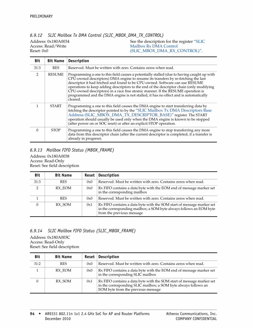
PRELIMINARY
6.9.12 SLIC Mailbox Tx DMA Control (SLIC_MBOX_DMA_TX_CONTROL)Address: 0x180A0034 Access: Read/Write Reset: 0x0
See the description for the register “SLIC Mailbox Rx DMA Control (SLIC_MBOX_DMA_RX_CONTROL)”.
6.9.13 Mailbox FIFO Status (MBOX_FRAME)Address: 0x180A0038 Access: Read-Only Reset: See field description
6.9.14 SLIC Mailbox FIFO Status (SLIC_MBOX_FRAME)Address: 0x180A003C Access: Read-Only Reset: See field description
Bit Bit Name Description
31:3 RES Reserved. Must be written with zero. Contains zeros when read.
2 RESUME Programming a one to this field causes a potentially stalled (due to having caught up with CPU-owned descriptors) DMA engine to resume its transfers by re-fetching the last descriptor it had fetched and found to be CPU-owned. Software can use RESUME operations to keep adding descriptors to the end of the descriptor chain (only modifying CPU-owned descriptors) in a race free atomic manner. If the RESUME operation is programmed and the DMA engine is not stalled, it has no effect and is automatically cleared.
1 START Programming a one to this field causes the DMA engine to start transferring data by fetching the descriptor pointed to by the “SLIC Mailbox Tx DMA Descriptors Base Address (SLIC_MBOX_DMA_TX_DESCRIPTOR_BASE)” register. The START operation should usually be used only when the DMA engine is known to be stopped (after power on or SOC reset) or after an explicit STOP operation.
0 STOP Programming a one to this field causes the DMA engine to stop transferring any more data from this descriptor chain (after the current descriptor is completed, if a transfer is already in progress).
Bit Bit Name Reset Description31:3 RES 0x0 Reserved. Must be written with zero. Contains zeros when read.
2 RX_EOM 0x0 Rx FIFO contains a data byte with the EOM end of message marker set in the corresponding mailbox
1 RES 0x0 Reserved. Must be written with zero. Contains zeros when read.
0 RX_SOM 0x1 Rx FIFO contains a data byte with the SOM start of message marker set in the corresponding mailbox; a SOM byte always follows an EOM byte from the previous message
Bit Bit Name Reset Description
31:2 RES 0x0 Reserved. Must be written with zero. Contains zeros when read.
1 RX_EOM 0x0 Rx FIFO contains a data byte with the EOM end of message marker set in the corresponding SLIC mailbox
0 RX_SOM 0x1 Rx FIFO contains a data byte with the SOM start of message marker set in the corresponding SLIC mailbox; a SOM byte always follows an EOM byte from the previous message
94 • AR9331 802.11n 1x1 2.4 GHz SoC for AP and Router Platforms Atheros Communications, Inc. 94 • December 2010 COMPANY CONFIDENTIAL
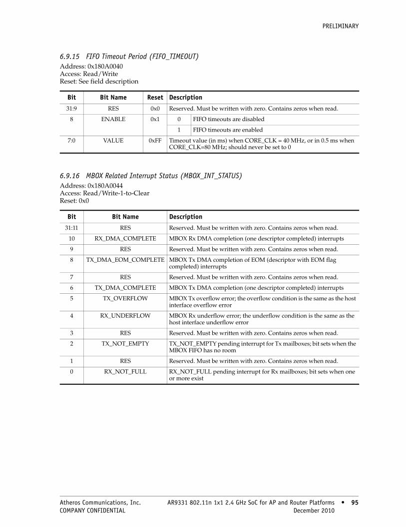
PRELIMINARY
6.9.15 FIFO Timeout Period (FIFO_TIMEOUT)Address: 0x180A0040 Access: Read/Write Reset: See field description
6.9.16 MBOX Related Interrupt Status (MBOX_INT_STATUS)Address: 0x180A0044 Access: Read/Write-1-to-Clear Reset: 0x0
Bit Bit Name Reset Description
31:9 RES 0x0 Reserved. Must be written with zero. Contains zeros when read.
8 ENABLE 0x1 0 FIFO timeouts are disabled
1 FIFO timeouts are enabled
7:0 VALUE 0xFF Timeout value (in ms) when CORE_CLK = 40 MHz, or in 0.5 ms when CORE_CLK=80 MHz; should never be set to 0
Bit Bit Name Description
31:11 RES Reserved. Must be written with zero. Contains zeros when read.
10 RX_DMA_COMPLETE MBOX Rx DMA completion (one descriptor completed) interrupts
9 RES Reserved. Must be written with zero. Contains zeros when read.
8 TX_DMA_EOM_COMPLETE MBOX Tx DMA completion of EOM (descriptor with EOM flag completed) interrupts
7 RES Reserved. Must be written with zero. Contains zeros when read.
6 TX_DMA_COMPLETE MBOX Tx DMA completion (one descriptor completed) interrupts
5 TX_OVERFLOW MBOX Tx overflow error; the overflow condition is the same as the host interface overflow error
4 RX_UNDERFLOW MBOX Rx underflow error; the underflow condition is the same as the host interface underflow error
3 RES Reserved. Must be written with zero. Contains zeros when read.
2 TX_NOT_EMPTY TX_NOT_EMPTY pending interrupt for Tx mailboxes; bit sets when the MBOX FIFO has no room
1 RES Reserved. Must be written with zero. Contains zeros when read.
0 RX_NOT_FULL RX_NOT_FULL pending interrupt for Rx mailboxes; bit sets when one or more exist
Atheros Communications, Inc. AR9331 802.11n 1x1 2.4 GHz SoC for AP and Router Platforms • 95 COMPANY CONFIDENTIAL December 2010 • 95

PRELIMINARY
6.9.17 SLIC MBOX Related Interrupt Status (SLIC_MBOX_INT_STATUS)Address: 0x180A0048 Access: Read/Write-1-to-Clear Reset: 0x0
6.9.18 MBOX Related Interrupt Enables (MBOX_INT_ENABLE)Address: 0x180A004C Access: Read/Write Reset: 0x0
This register is used to mask/enable interrupts to the CPU.
Bit Bit Name Description
31:7 RES Reserved. Must be written with zero. Contains zeros when read.
6 RX_DMA_COMPLETE SLIC mailbox Rx DMA completion (one descriptor completed) interrupts
5 TX_DMA_EOM_COMPLETE SLIC mailbox Tx DMA completion of EOM (descriptor with EOM flag completed) interrupts
4 TX_DMA_COMPLETE SLIC mailbox Tx DMA completion (one descriptor completed) interrupts
3 TX_OVERFLOW SLIC MBOX Tx overflow error; the overflow condition is the same as the host interface overflow error
2 RX_UNDERFLOW SLIC MBOX Rx underflow error; the underflow condition is the same as the host interface underflow error
1 TX_NOT_EMPTY TX_NOT_EMPTY pending interrupt for SLIC Tx mailboxes; bit sets when the MBOX FIFO has no room
0 RX_NOT_FULL RX_NOT_FULL pending interrupt for SLIC Rx mailboxes; bit sets when one or more exist
Bit Bit Name Description
31:11 RES Reserved. Must be written with zero. Contains zeros when read.
10 RX_DMA_COMPLETE Enable mailbox Rx DMA completion interrupts
9 RES Reserved. Must be written with zero. Contains zeros when read.
8 TX_DMA_EOM_COMPLETE Enable mailbox Tx DMA completion of end of message interrupts
7 RES Reserved. Must be written with zero. Contains zeros when read.
6 TX_DMA_COMPLETE Enable mailbox Tx DMA completion interrupts
5 TX_OVERFLOW Enable MBOX Tx overflow error
4 RX_UNDERFLOW Enable MBOX Rx overflow error
3 RES Reserved. Must be written with zero. Contains zeros when read.
2 TX_NOT_EMPTY Enable TX_NOT_EMPTY interrupts from MBOX Tx FIFOs
1 RES Reserved. Must be written with zero. Contains zeros when read.
0 RX_NOT_FULL Enable RX_NOT_EMPTY interrupts from MBOX RX FIFOs
96 • AR9331 802.11n 1x1 2.4 GHz SoC for AP and Router Platforms Atheros Communications, Inc. 96 • December 2010 COMPANY CONFIDENTIAL
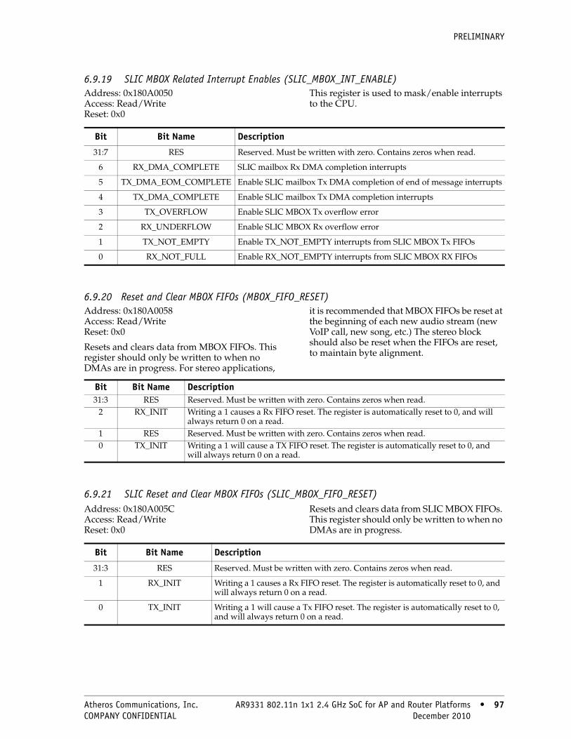
PRELIMINARY
6.9.19 SLIC MBOX Related Interrupt Enables (SLIC_MBOX_INT_ENABLE)Address: 0x180A0050 Access: Read/Write Reset: 0x0
This register is used to mask/enable interrupts to the CPU.
6.9.20 Reset and Clear MBOX FIFOs (MBOX_FIFO_RESET)Address: 0x180A0058 Access: Read/Write Reset: 0x0
Resets and clears data from MBOX FIFOs. This register should only be written to when no DMAs are in progress. For stereo applications,
it is recommended that MBOX FIFOs be reset at the beginning of each new audio stream (new VoIP call, new song, etc.) The stereo block should also be reset when the FIFOs are reset, to maintain byte alignment.
6.9.21 SLIC Reset and Clear MBOX FIFOs (SLIC_MBOX_FIFO_RESET)Address: 0x180A005C Access: Read/Write Reset: 0x0
Resets and clears data from SLIC MBOX FIFOs. This register should only be written to when no DMAs are in progress.
Bit Bit Name Description
31:7 RES Reserved. Must be written with zero. Contains zeros when read.
6 RX_DMA_COMPLETE SLIC mailbox Rx DMA completion interrupts
5 TX_DMA_EOM_COMPLETE Enable SLIC mailbox Tx DMA completion of end of message interrupts
4 TX_DMA_COMPLETE Enable SLIC mailbox Tx DMA completion interrupts
3 TX_OVERFLOW Enable SLIC MBOX Tx overflow error
2 RX_UNDERFLOW Enable SLIC MBOX Rx overflow error
1 TX_NOT_EMPTY Enable TX_NOT_EMPTY interrupts from SLIC MBOX Tx FIFOs
0 RX_NOT_FULL Enable RX_NOT_EMPTY interrupts from SLIC MBOX RX FIFOs
Bit Bit Name Description31:3 RES Reserved. Must be written with zero. Contains zeros when read.
2 RX_INIT Writing a 1 causes a Rx FIFO reset. The register is automatically reset to 0, and will always return 0 on a read.
1 RES Reserved. Must be written with zero. Contains zeros when read.0 TX_INIT Writing a 1 will cause a TX FIFO reset. The register is automatically reset to 0, and
will always return 0 on a read.
Bit Bit Name Description
31:3 RES Reserved. Must be written with zero. Contains zeros when read.
1 RX_INIT Writing a 1 causes a Rx FIFO reset. The register is automatically reset to 0, and will always return 0 on a read.
0 TX_INIT Writing a 1 will cause a Tx FIFO reset. The register is automatically reset to 0, and will always return 0 on a read.
Atheros Communications, Inc. AR9331 802.11n 1x1 2.4 GHz SoC for AP and Router Platforms • 97 COMPANY CONFIDENTIAL December 2010 • 97
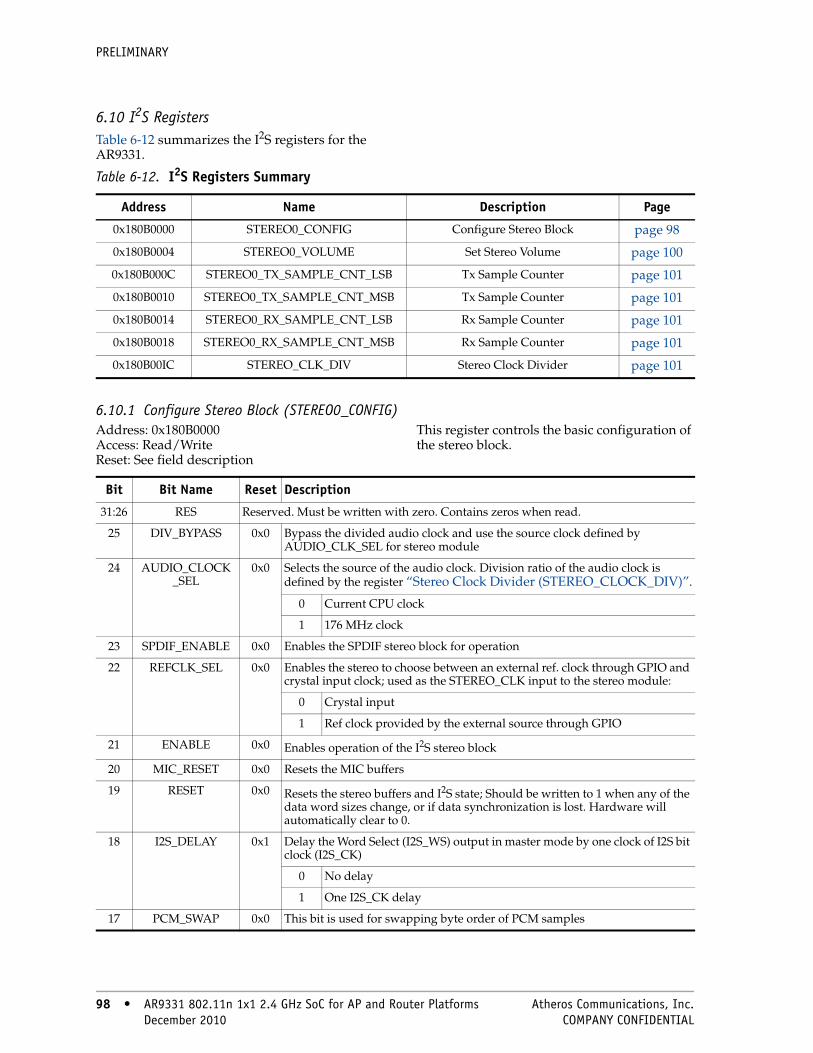
PRELIMINARY
6.10 I2S RegistersTable 6-12 summarizes the I2S registers for the AR9331.
6.10.1 Configure Stereo Block (STEREO0_CONFIG)Address: 0x180B0000 Access: Read/Write Reset: See field description
This register controls the basic configuration of the stereo block.
Table 6-12. I2S Registers Summary
Address Name Description Page
0x180B0000 STEREO0_CONFIG Configure Stereo Block page 98
0x180B0004 STEREO0_VOLUME Set Stereo Volume page 100
0x180B000C STEREO0_TX_SAMPLE_CNT_LSB Tx Sample Counter page 101
0x180B0010 STEREO0_TX_SAMPLE_CNT_MSB Tx Sample Counter page 101
0x180B0014 STEREO0_RX_SAMPLE_CNT_LSB Rx Sample Counter page 101
0x180B0018 STEREO0_RX_SAMPLE_CNT_MSB Rx Sample Counter page 101
0x180B00IC STEREO_CLK_DIV Stereo Clock Divider page 101
Bit Bit Name Reset Description
31:26 RES Reserved. Must be written with zero. Contains zeros when read.
25 DIV_BYPASS 0x0 Bypass the divided audio clock and use the source clock defined by AUDIO_CLK_SEL for stereo module
24 AUDIO_CLOCK_SEL
0x0 Selects the source of the audio clock. Division ratio of the audio clock is defined by the register “Stereo Clock Divider (STEREO_CLOCK_DIV)”.
0 Current CPU clock
1 176 MHz clock
23 SPDIF_ENABLE 0x0 Enables the SPDIF stereo block for operation
22 REFCLK_SEL 0x0 Enables the stereo to choose between an external ref. clock through GPIO and crystal input clock; used as the STEREO_CLK input to the stereo module:
0 Crystal input
1 Ref clock provided by the external source through GPIO
21 ENABLE 0x0 Enables operation of the I2S stereo block
20 MIC_RESET 0x0 Resets the MIC buffers
19 RESET 0x0 Resets the stereo buffers and I2S state; Should be written to 1 when any of the data word sizes change, or if data synchronization is lost. Hardware will automatically clear to 0.
18 I2S_DELAY 0x1 Delay the Word Select (I2S_WS) output in master mode by one clock of I2S bit clock (I2S_CK)
0 No delay
1 One I2S_CK delay
17 PCM_SWAP 0x0 This bit is used for swapping byte order of PCM samples
98 • AR9331 802.11n 1x1 2.4 GHz SoC for AP and Router Platforms Atheros Communications, Inc. 98 • December 2010 COMPANY CONFIDENTIAL
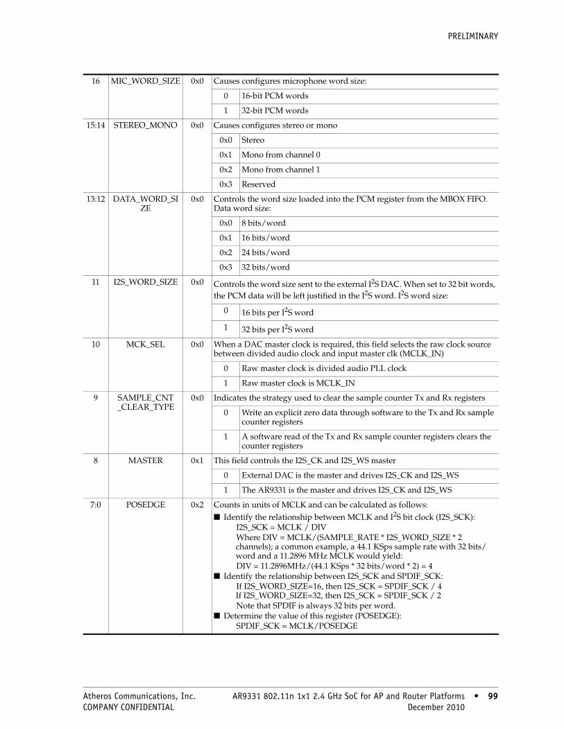
PRELIMINARY
16 MIC_WORD_SIZE 0x0 Causes configures microphone word size:
0 16-bit PCM words
1 32-bit PCM words
15:14 STEREO_MONO 0x0 Causes configures stereo or mono
0x0 Stereo
0x1 Mono from channel 0
0x2 Mono from channel 1
0x3 Reserved
13:12 DATA_WORD_SIZE
0x0 Controls the word size loaded into the PCM register from the MBOX FIFO. Data word size:
0x0 8 bits/word
0x1 16 bits/word
0x2 24 bits/word
0x3 32 bits/word
11 I2S_WORD_SIZE 0x0 Controls the word size sent to the external I2S DAC. When set to 32 bit words, the PCM data will be left justified in the I2S word. I2S word size:
0 16 bits per I2S word
1 32 bits per I2S word
10 MCK_SEL 0x0 When a DAC master clock is required, this field selects the raw clock source between divided audio clock and input master clk (MCLK_IN)
0 Raw master clock is divided audio PLL clock
1 Raw master clock is MCLK_IN
9 SAMPLE_CNT_CLEAR_TYPE
0x0 Indicates the strategy used to clear the sample counter Tx and Rx registers
0 Write an explicit zero data through software to the Tx and Rx sample counter registers
1 A software read of the Tx and Rx sample counter registers clears the counter registers
8 MASTER 0x1 This field controls the I2S_CK and I2S_WS master
0 External DAC is the master and drives I2S_CK and I2S_WS
1 The AR9331 is the master and drives I2S_CK and I2S_WS
7:0 POSEDGE 0x2 Counts in units of MCLK and can be calculated as follows:■ Identify the relationship between MCLK and I2S bit clock (I2S_SCK):
I2S_SCK = MCLK / DIV Where DIV = MCLK/(SAMPLE_RATE * I2S_WORD_SIZE * 2 channels); a common example, a 44.1 KSps sample rate with 32 bits/word and a 11.2896 MHz MCLK would yield:DIV = 11.2896MHz/(44.1 KSps * 32 bits/word * 2) = 4
■ Identify the relationship between I2S_SCK and SPDIF_SCK:If I2S_WORD_SIZE=16, then I2S_SCK = SPDIF_SCK / 4 If I2S_WORD_SIZE=32, then I2S_SCK = SPDIF_SCK / 2Note that SPDIF is always 32 bits per word.
■ Determine the value of this register (POSEDGE):SPDIF_SCK = MCLK/POSEDGE
Atheros Communications, Inc. AR9331 802.11n 1x1 2.4 GHz SoC for AP and Router Platforms • 99 COMPANY CONFIDENTIAL December 2010 • 99

PRELIMINARY
6.10.2 Set Stereo Volume (STEREO0_VOLUME)Address: 0x180B0004 Access: Read/Write Reset: 0x0
This register digitally attenuates or increases the volume level of the stereo output. Volume is adjusted in 3-db steps. If the gain is set too high, the PCM values saturate and waveform clipping occurs.
Bit Bit Name Description
31:13 RES Reserved. Must be written with zero. Contains zeros when read.
12:8 CHANNEL1 Channel 1 gain/attenuation. Setting the gain above +7 is not supported. A 5 bit number; the MSB is a sign bit, the others are magnitude:
Binary (Decimal) Result
11111 (–16) Maximum attenuation
11110 (–14) –84 dB
... ...
10001 (–1) –6 dB
10000 (0) 0 dB
00000 (0) 0 dB
00001 (+1) +6 dB
... ...
00111 (+7) +42 dB (maximum gain)
01000 (+8) Reserved
... ...
01111 (+15) Reserved
7:5 RES Reserved. Must be written with zero. Contains zeros when read.
4:0 CHANNEL0 Channel 0 gain/attenuation. Setting the gain above +7 is not supported. A 5 bit number; the MSB is a sign bit, the others are magnitude:
Binary (Decimal) Result
11111 (–16) Maximum attenuation
11110 –14) –84 dB
... ...
10001 (–1) –6 dB
10000 (0) 0 dB
00000 (0) 0 dB
00001 (+1) +6 dB
... ...
00111 (+7) +42 dB (maximum gain)
01000 (+8) Reserved
... ...
... ...
01111 (+15) Reserved
100 • AR9331 802.11n 1x1 2.4 GHz SoC for AP and Router Platforms Atheros Communications, Inc. 100 • December 2010 COMPANY CONFIDENTIAL
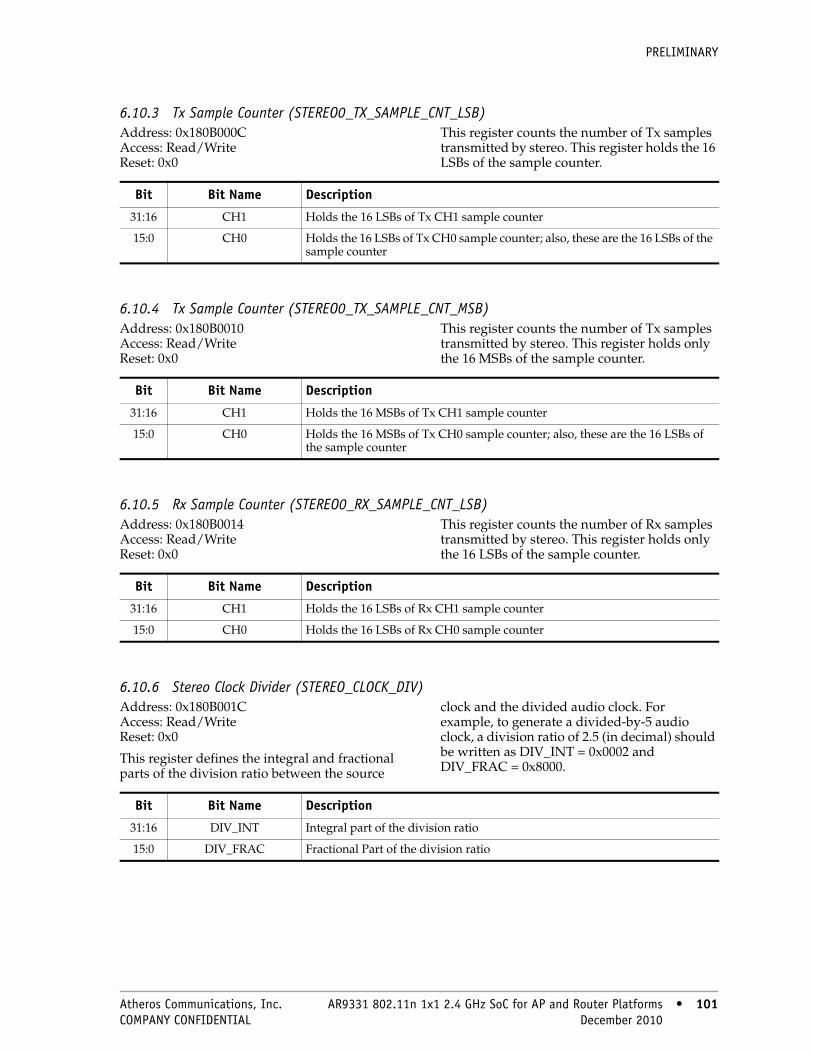
PRELIMINARY
6.10.3 Tx Sample Counter (STEREO0_TX_SAMPLE_CNT_LSB)Address: 0x180B000C Access: Read/Write Reset: 0x0
This register counts the number of Tx samples transmitted by stereo. This register holds the 16 LSBs of the sample counter.
6.10.4 Tx Sample Counter (STEREO0_TX_SAMPLE_CNT_MSB)Address: 0x180B0010 Access: Read/Write Reset: 0x0
This register counts the number of Tx samples transmitted by stereo. This register holds only the 16 MSBs of the sample counter.
6.10.5 Rx Sample Counter (STEREO0_RX_SAMPLE_CNT_LSB)Address: 0x180B0014 Access: Read/Write Reset: 0x0
This register counts the number of Rx samples transmitted by stereo. This register holds only the 16 LSBs of the sample counter.
6.10.6 Stereo Clock Divider (STEREO_CLOCK_DIV)Address: 0x180B001C Access: Read/Write Reset: 0x0
This register defines the integral and fractional parts of the division ratio between the source
clock and the divided audio clock. For example, to generate a divided-by-5 audio clock, a division ratio of 2.5 (in decimal) should be written as DIV_INT = 0x0002 and DIV_FRAC = 0x8000.
Bit Bit Name Description
31:16 CH1 Holds the 16 LSBs of Tx CH1 sample counter
15:0 CH0 Holds the 16 LSBs of Tx CH0 sample counter; also, these are the 16 LSBs of the sample counter
Bit Bit Name Description
31:16 CH1 Holds the 16 MSBs of Tx CH1 sample counter
15:0 CH0 Holds the 16 MSBs of Tx CH0 sample counter; also, these are the 16 LSBs of the sample counter
Bit Bit Name Description
31:16 CH1 Holds the 16 LSBs of Rx CH1 sample counter
15:0 CH0 Holds the 16 LSBs of Rx CH0 sample counter
Bit Bit Name Description
31:16 DIV_INT Integral part of the division ratio
15:0 DIV_FRAC Fractional Part of the division ratio
Atheros Communications, Inc. AR9331 802.11n 1x1 2.4 GHz SoC for AP and Router Platforms • 101 COMPANY CONFIDENTIAL December 2010 • 101
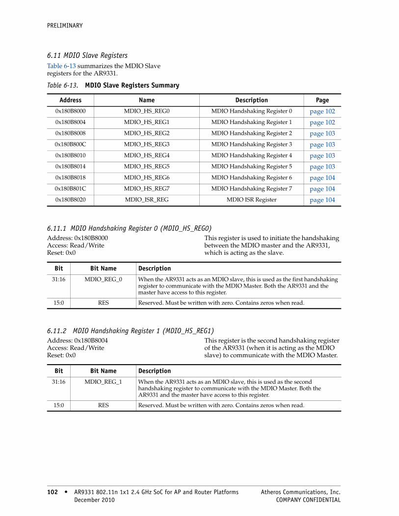
PRELIMINARY
6.11 MDIO Slave RegistersTable 6-13 summarizes the MDIO Slave registers for the AR9331.
6.11.1 MDIO Handshaking Register 0 (MDIO_HS_REG0)Address: 0x180B8000 Access: Read/Write Reset: 0x0
This register is used to initiate the handshaking between the MDIO master and the AR9331, which is acting as the slave.
6.11.2 MDIO Handshaking Register 1 (MDIO_HS_REG1)Address: 0x180B8004 Access: Read/Write Reset: 0x0
This register is the second handshaking register of the AR9331 (when it is acting as the MDIO slave) to communicate with the MDIO Master.
Table 6-13. MDIO Slave Registers Summary
Address Name Description Page
0x180B8000 MDIO_HS_REG0 MDIO Handshaking Register 0 page 102
0x180B8004 MDIO_HS_REG1 MDIO Handshaking Register 1 page 102
0x180B8008 MDIO_HS_REG2 MDIO Handshaking Register 2 page 103
0x180B800C MDIO_HS_REG3 MDIO Handshaking Register 3 page 103
0x180B8010 MDIO_HS_REG4 MDIO Handshaking Register 4 page 103
0x180B8014 MDIO_HS_REG5 MDIO Handshaking Register 5 page 103
0x180B8018 MDIO_HS_REG6 MDIO Handshaking Register 6 page 104
0x180B801C MDIO_HS_REG7 MDIO Handshaking Register 7 page 104
0x180B8020 MDIO_ISR_REG MDIO ISR Register page 104
Bit Bit Name Description
31:16 MDIO_REG_0 When the AR9331 acts as an MDIO slave, this is used as the first handshaking register to communicate with the MDIO Master. Both the AR9331 and the master have access to this register.
15:0 RES Reserved. Must be written with zero. Contains zeros when read.
Bit Bit Name Description
31:16 MDIO_REG_1 When the AR9331 acts as an MDIO slave, this is used as the second handshaking register to communicate with the MDIO Master. Both the AR9331 and the master have access to this register.
15:0 RES Reserved. Must be written with zero. Contains zeros when read.
102 • AR9331 802.11n 1x1 2.4 GHz SoC for AP and Router Platforms Atheros Communications, Inc. 102 • December 2010 COMPANY CONFIDENTIAL

PRELIMINARY
6.11.3 MDIO Handshaking Register 2 (MDIO_HS_REG2)Address: 0x180B8008 Access: Read/Write Reset: 0x0
This register is the third handshaking register of the AR9331 (when it is acting as the MDIO slave) to communicate with the MDIO Master.
6.11.4 MDIO Handshaking Register 3 (MDIO_HS_REG3)Address: 0x180B800C Access: Read/Write Reset: 0x0
This register is the fourth handshaking register of the AR9331 (when it is acting as the MDIO slave) to communicate with the MDIO Master.
6.11.5 MDIO Handshaking Register 4 (MDIO_HS_REG4)Address: 0x180B8010 Access: Read/Write Reset: 0x0
This register is the fifth handshaking register of the AR9331 (when it is acting as the MDIO slave) to communicate with the MDIO Master.
6.11.6 MDIO Handshaking Register 5 (MDIO_HS_REG5)Address: 0x180B8014 Access: Read/Write Reset: 0x0
This register is the sixth handshaking register of the AR9331 (when it is acting as the MDIO slave) to communicate with the MDIO Master.
Bit Bit Name Description
31:16 MDIO_REG_2 When the AR9331 acts as an MDIO slave, this is used as the third handshaking register to communicate with the MDIO Master. Both the AR9331 and the master have access to this register.
15:0 RES Reserved. Must be written with zero. Contains zeros when read.
Bit Bit Name Description
31:16 MDIO_REG_3 When the AR9331 acts as an MDIO slave, this is used as the fourth handshaking register to communicate with the MDIO Master. Both the AR9331 and the master have access to this register.
15:0 RES Reserved. Must be written with zero. Contains zeros when read.
Bit Bit Name Description
31:16 MDIO_REG_4 When the AR9331 acts as an MDIO slave, this is used as the fifth handshaking register to communicate with the MDIO Master. Both the AR9331 and the master have access to this register.
15:0 RES Reserved. Must be written with zero. Contains zeros when read.
Bit Bit Name Description
31:16 MDIO_REG_5 When the AR9331 acts as an MDIO slave, this is used as the sixth handshaking register to communicate with the MDIO Master. Both the AR9331 and the master have access to this register.
15:0 RES Reserved. Must be written with zero. Contains zeros when read.
Atheros Communications, Inc. AR9331 802.11n 1x1 2.4 GHz SoC for AP and Router Platforms • 103 COMPANY CONFIDENTIAL December 2010 • 103

PRELIMINARY
6.11.7 MDIO Handshaking Register 6 (MDIO_HS_REG6)Address: 0x180B8018 Access: Read/Write Reset: 0x0
This register is the seventh handshaking register of the AR9331 (when it is acting as the MDIO slave) to communicate with the MDIO Master.
6.11.8 MDIO Handshaking Register 7 (MDIO_HS_REG7)Address: 0x180B001C Access: Read/Write Reset: 0x0
This register is the eighth handshaking register of the AR9331 (when it is acting as the MDIO slave) to communicate with the MDIO Master.
6.11.9 MDIO ISR Register (MDIO_ISR_REG)Address: 0x180B8020 Access: Read Only Reset: 0x0
This register is used to notify that one of the previous MDIO Handshaking registers has been written by the MDIO master.
Bit Bit Name Description
31:16 MDIO_REG_6 When the AR9331 acts as an MDIO slave, this is used as the seventh handshaking register to communicate with the MDIO Master. Both the AR9331 and the master have access to this register.
15:0 RES Reserved. Must be written with zero. Contains zeros when read.
Bit Bit Name Description
31:16 MDIO_REG_7 When the AR9331 acts as an MDIO slave, this is used as the eighth handshaking register to communicate with the MDIO Master. Both the AR9331 and the master have access to this register.
15:0 RES Reserved. Must be written with zero. Contains zeros when read.
Bit Bit Name Description
31:8 RES Reserved. Must be written with zero. Contains zeros when read.
7 MASTER_ACC_IND0 Indicates MDIO Handshaking Register 0 has been written by the MDIO master.
6 MASTER_ACC_IND1 Indicates MDIO Handshaking Register 1 has been written by the MDIO master.
5 MASTER_ACC_IND2 Indicates MDIO Handshaking Register 2 has been written by the MDIO master.
4 MASTER_ACC_IND3 Indicates MDIO Handshaking Register 3 has been written by the MDIO master.
3 MASTER_ACC_IND4 Indicates MDIO Handshaking Register 4 has been written by the MDIO master.
2 MASTER_ACC_IND5 Indicates MDIO Handshaking Register 5 has been written by the MDIO master.
1 MASTER_ACC_IND6 Indicates MDIO Handshaking Register 6 has been written by the MDIO master.
0 MASTER_ACC_IND7 Indicates MDIO Handshaking Register 7 has been written by the MDIO master.
104 • AR9331 802.11n 1x1 2.4 GHz SoC for AP and Router Platforms Atheros Communications, Inc. 104 • December 2010 COMPANY CONFIDENTIAL

PRELIMINARY
6.12 General DMA and Rx-Related RegistersTable 6-14 shows the mapping of the general DMA and Rx-related (MAC interface) registers.
Table 6-14. General DMA and Rx-Related Registers
Offset Name Description Page
0x18100008 CR Command page 106
0x18100014 CFG Configuration and Status page 107
0x18100018 RXBUFPTR_THRESH Rx DMA Data Buffer Pointer Threshold page 108
0x1810001C TXDPPTR_THRESH Tx DMA Descriptor Pointer Threshold page 108
0x18100020 MIRT Maximum Interrupt Rate Threshold page 108
0x18100024 IER Interrupt Global Enable page 109
0x18100028 TIMT Tx Interrupt Mitigation Thresholds page 109
0x1810002C RIMT Rx Interrupt Mitigation Thresholds page 109
0x18100030 TXCFG Transmit Configuration page 110
0x18100034 RXCFG Receive Configuration page 110
0x18100040 MIBC MIB Control page 111
0x18100044 TOPS Timeout Prescale page 111
0x18100064 GTT Global Transmit Timeout page 111
0x18100068 GTTM Global Transmit Timeout Mode page 111
0x1810006C CST Carrier Sense Timeout page 112
0x18100070 RXDP_SIZE Size of High and Low Priority page 112
0x18100074 RX_QUEUE_HP_RXDP Lower 32 bits of MAC Rx High Priority Queue RXDP Pointer
page 112
0x18100078 RX_QUEUE_LP_RXDP Lower 32 bits of MAC Rx Low Priority Queue RXDP Pointer
page 112
0x18100080 ISR_P Primary Interrupt Status page 113
0x18100084 ISR_S0 Secondary Interrupt Status 0 page 114
0x18100088 ISR_S1 Secondary Interrupt Status 1 page 114
0x1810008C ISR_S2 Secondary Interrupt Status 2 page 115
0x18100090 ISR_S3 Secondary Interrupt Status 3 page 116
0x18100094 ISR_S4 Secondary Interrupt Status 4 page 116
0x18100098 ISR_S5 Secondary Interrupt Status 5 page 116
0x181000A0 IMR_P Primary Interrupt Mask page 117
0x181000A4 IMR_S0 Secondary Interrupt Mask 0 page 118
0x181000A8 IMR_S1 Secondary Interrupt Mask 1 page 118
0x181000AC IMR_S2 Secondary Interrupt Mask 2 page 119
0x181000B0 IMR_S3 Secondary Interrupt Mask 3 page 120
0x181000B4 IMR_S4 Secondary Interrupt Mask 4 page 120
Atheros Communications, Inc. AR9331 802.11n 1x1 2.4 GHz SoC for AP and Router Platforms • 105 COMPANY CONFIDENTIAL December 2010 • 105
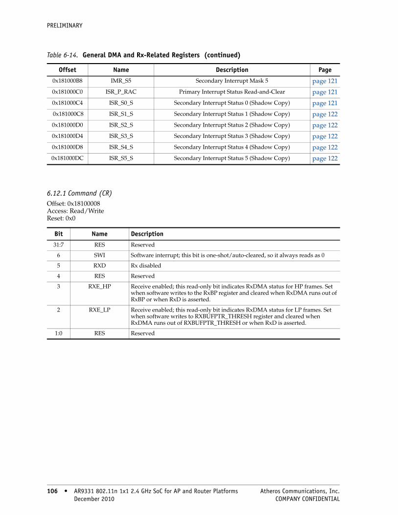
PRELIMINARY
6.12.1 Command (CR)Offset: 0x18100008 Access: Read/Write Reset: 0x0
0x181000B8 IMR_S5 Secondary Interrupt Mask 5 page 121
0x181000C0 ISR_P_RAC Primary Interrupt Status Read-and-Clear page 121
0x181000C4 ISR_S0_S Secondary Interrupt Status 0 (Shadow Copy) page 121
0x181000C8 ISR_S1_S Secondary Interrupt Status 1 (Shadow Copy) page 122
0x181000D0 ISR_S2_S Secondary Interrupt Status 2 (Shadow Copy) page 122
0x181000D4 ISR_S3_S Secondary Interrupt Status 3 (Shadow Copy) page 122
0x181000D8 ISR_S4_S Secondary Interrupt Status 4 (Shadow Copy) page 122
0x181000DC ISR_S5_S Secondary Interrupt Status 5 (Shadow Copy) page 122
Table 6-14. General DMA and Rx-Related Registers (continued)
Offset Name Description Page
Bit Name Description
31:7 RES Reserved
6 SWI Software interrupt; this bit is one-shot/auto-cleared, so it always reads as 0
5 RXD Rx disabled
4 RES Reserved
3 RXE_HP Receive enabled; this read-only bit indicates RxDMA status for HP frames. Set when software writes to the RxBP register and cleared when RxDMA runs out of RxBP or when RxD is asserted.
2 RXE_LP Receive enabled; this read-only bit indicates RxDMA status for LP frames. Set when software writes to RXBUFPTR_THRESH register and cleared when RxDMA runs out of RXBUFPTR_THRESH or when RxD is asserted.
1:0 RES Reserved
106 • AR9331 802.11n 1x1 2.4 GHz SoC for AP and Router Platforms Atheros Communications, Inc. 106 • December 2010 COMPANY CONFIDENTIAL
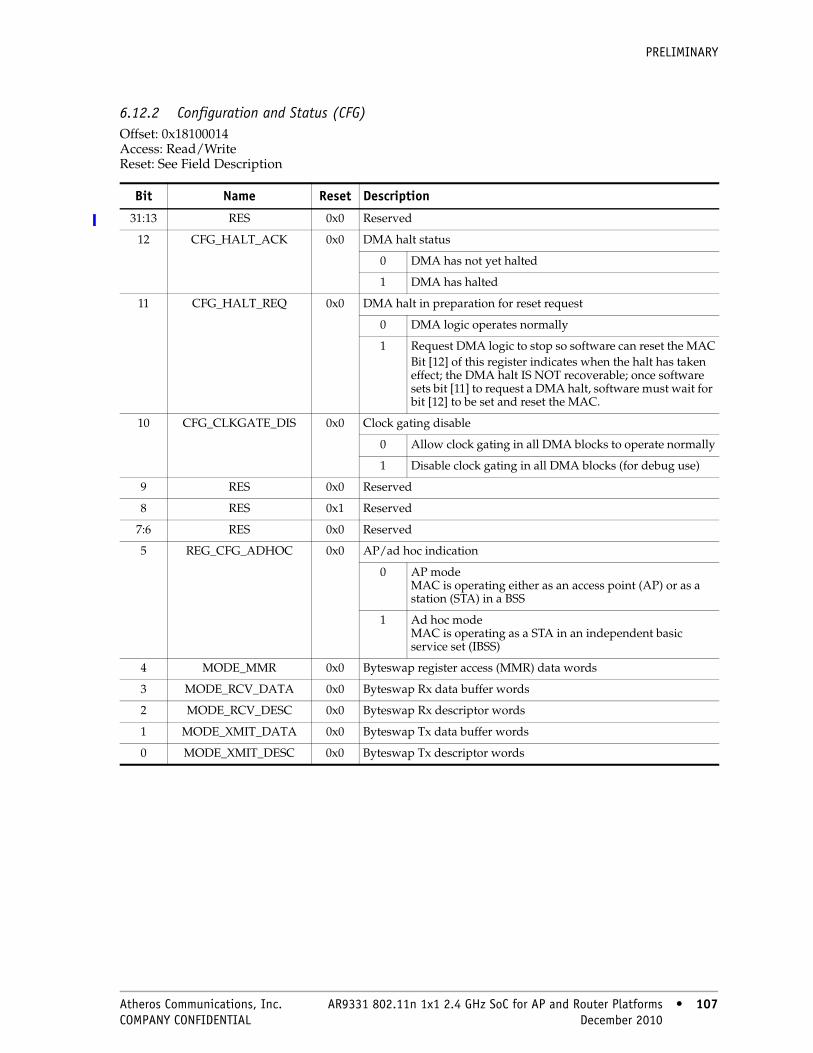
PRELIMINARY
6.12.2 Configuration and Status (CFG)Offset: 0x18100014 Access: Read/Write Reset: See Field Description
Bit Name Reset Description
31:13 RES 0x0 Reserved
12 CFG_HALT_ACK 0x0 DMA halt status
0 DMA has not yet halted
1 DMA has halted
11 CFG_HALT_REQ 0x0 DMA halt in preparation for reset request
0 DMA logic operates normally
1 Request DMA logic to stop so software can reset the MACBit [12] of this register indicates when the halt has taken effect; the DMA halt IS NOT recoverable; once software sets bit [11] to request a DMA halt, software must wait for bit [12] to be set and reset the MAC.
10 CFG_CLKGATE_DIS 0x0 Clock gating disable
0 Allow clock gating in all DMA blocks to operate normally
1 Disable clock gating in all DMA blocks (for debug use)
9 RES 0x0 Reserved
8 RES 0x1 Reserved
7:6 RES 0x0 Reserved
5 REG_CFG_ADHOC 0x0 AP/ad hoc indication
0 AP mode MAC is operating either as an access point (AP) or as a station (STA) in a BSS
1 Ad hoc mode MAC is operating as a STA in an independent basic service set (IBSS)
4 MODE_MMR 0x0 Byteswap register access (MMR) data words
3 MODE_RCV_DATA 0x0 Byteswap Rx data buffer words
2 MODE_RCV_DESC 0x0 Byteswap Rx descriptor words
1 MODE_XMIT_DATA 0x0 Byteswap Tx data buffer words
0 MODE_XMIT_DESC 0x0 Byteswap Tx descriptor words
Atheros Communications, Inc. AR9331 802.11n 1x1 2.4 GHz SoC for AP and Router Platforms • 107 COMPANY CONFIDENTIAL December 2010 • 107
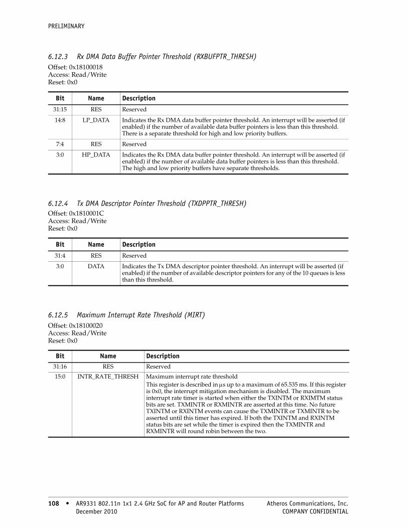
PRELIMINARY
6.12.3 Rx DMA Data Buffer Pointer Threshold (RXBUFPTR_THRESH)Offset: 0x18100018 Access: Read/Write Reset: 0x0
6.12.4 Tx DMA Descriptor Pointer Threshold (TXDPPTR_THRESH)Offset: 0x1810001C Access: Read/Write Reset: 0x0
6.12.5 Maximum Interrupt Rate Threshold (MIRT)Offset: 0x18100020 Access: Read/Write Reset: 0x0
Bit Name Description
31:15 RES Reserved
14:8 LP_DATA Indicates the Rx DMA data buffer pointer threshold. An interrupt will be asserted (if enabled) if the number of available data buffer pointers is less than this threshold. There is a separate threshold for high and low priority buffers.
7:4 RES Reserved
3:0 HP_DATA Indicates the Rx DMA data buffer pointer threshold. An interrupt will be asserted (if enabled) if the number of available data buffer pointers is less than this threshold. The high and low priority buffers have separate thresholds.
Bit Name Description
31:4 RES Reserved
3:0 DATA Indicates the Tx DMA descriptor pointer threshold. An interrupt will be asserted (if enabled) if the number of available descriptor pointers for any of the 10 queues is less than this threshold.
Bit Name Description31:16 RES Reserved
15:0 INTR_RATE_THRESH Maximum interrupt rate thresholdThis register is described in μs up to a maximum of 65.535 ms. If this register is 0x0, the interrupt mitigation mechanism is disabled. The maximum interrupt rate timer is started when either the TXINTM or RXIMTM status bits are set. TXMINTR or RXMINTR are asserted at this time. No future TXINTM or RXINTM events can cause the TXMINTR or TXMINTR to be asserted until this timer has expired. If both the TXINTM and RXINTM status bits are set while the timer is expired then the TXMINTR and RXMINTR will round robin between the two.
108 • AR9331 802.11n 1x1 2.4 GHz SoC for AP and Router Platforms Atheros Communications, Inc. 108 • December 2010 COMPANY CONFIDENTIAL
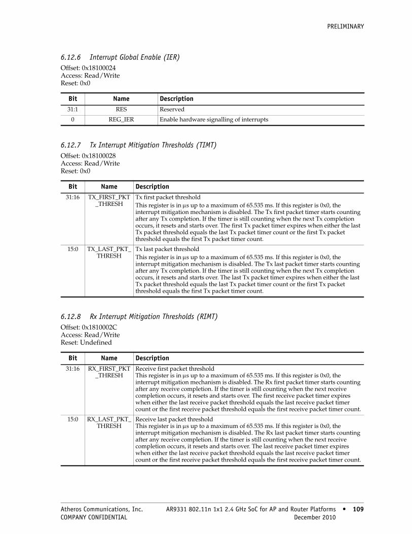
PRELIMINARY
6.12.6 Interrupt Global Enable (IER)Offset: 0x18100024 Access: Read/Write Reset: 0x0
6.12.7 Tx Interrupt Mitigation Thresholds (TIMT) Offset: 0x18100028 Access: Read/Write Reset: 0x0
6.12.8 Rx Interrupt Mitigation Thresholds (RIMT) Offset: 0x1810002C Access: Read/Write Reset: Undefined
Bit Name Description31:1 RES Reserved
0 REG_IER Enable hardware signalling of interrupts
Bit Name Description31:16 TX_FIRST_PKT
_THRESHTx first packet thresholdThis register is in μs up to a maximum of 65.535 ms. If this register is 0x0, the interrupt mitigation mechanism is disabled. The Tx first packet timer starts counting after any Tx completion. If the timer is still counting when the next Tx completion occurs, it resets and starts over. The first Tx packet timer expires when either the last Tx packet threshold equals the last Tx packet timer count or the first Tx packet threshold equals the first Tx packet timer count.
15:0 TX_LAST_PKT_THRESH
Tx last packet thresholdThis register is in μs up to a maximum of 65.535 ms. If this register is 0x0, the interrupt mitigation mechanism is disabled. The Tx last packet timer starts counting after any Tx completion. If the timer is still counting when the next Tx completion occurs, it resets and starts over. The last Tx packet timer expires when either the last Tx packet threshold equals the last Tx packet timer count or the first Tx packet threshold equals the first Tx packet timer count.
Bit Name Description31:16 RX_FIRST_PKT
_THRESHReceive first packet threshold This register is in μs up to a maximum of 65.535 ms. If this register is 0x0, the interrupt mitigation mechanism is disabled. The Rx first packet timer starts counting after any receive completion. If the timer is still counting when the next receive completion occurs, it resets and starts over. The first receive packet timer expires when either the last receive packet threshold equals the last receive packet timer count or the first receive packet threshold equals the first receive packet timer count.
15:0 RX_LAST_PKT_THRESH
Receive last packet threshold This register is in μs up to a maximum of 65.535 ms. If this register is 0x0, the interrupt mitigation mechanism is disabled. The Rx last packet timer starts counting after any receive completion. If the timer is still counting when the next receive completion occurs, it resets and starts over. The last receive packet timer expires when either the last receive packet threshold equals the last receive packet timer count or the first receive packet threshold equals the first receive packet timer count.
Atheros Communications, Inc. AR9331 802.11n 1x1 2.4 GHz SoC for AP and Router Platforms • 109 COMPANY CONFIDENTIAL December 2010 • 109

PRELIMINARY
6.12.9 Tx Configuration (TXCFG)Offset: 0x18100030 Access: Read/Write Reset: See Field Descriptions
6.12.10 Rx Configuration (RXCFG)Offset: 0x18100034 Access: Read/Write Reset: See Field Descriptions
Bit Name Reset Description31:18 RES 0x0 Reserved
17 DIS_RETRY_UNDERRUN
0x1 Disable retry of underrun packets
0 Underrun packets will retry indefinitely
1 Underrun packets will quit after first underrun attempt and write status indicating underrun
16:10 RES 0x0 Reserved
9:4 TXCFG_TRIGLVL 0x1 Frame trigger level Specifies the minimum number of bytes, in units of 64 bytes, which must be DMAed into the PCU TXFIFO before the PCU initiates sending the frame on the air. Resets to 0x1 (meaning 64 Bytes or a full frame, whichever occurs first).
3 RES 0x0 Reserved
2:0 TXCFG_DMA_SIZE 0x5 Maximum DMA request size for master reads
0 4 B
1 8 B
2 16 B
3 32 B
4 64 B
5 128 B
6 256 B
7 Reserved
Bit Name Reset Description31:5 RES 0x0 Reserved
4:3 ZERO_LEN_DMA_EN 0x0 Zero-length frame DMA enable
0 Disable DMA of all zero-length frames. In this mode, the DMA logic suppresses all zero-length frames. Reception of zero-length frames is invisible to the host (they neither appear in host memory nor consume a Rx descriptor).
1 Reserved
2 Enable DMA of all zero-length frames. In this mode, all zero-length frames (chirps, double-chirps, and non-chirps) are DMAed into host memory just like normal (non-zero-length) frames.
3 Reserved
2:0 DMA_SIZE 0x4 Maximum DMA size for master writes; (See the encodings for the register “Tx Configuration (TXCFG)” on page 110)
110 • AR9331 802.11n 1x1 2.4 GHz SoC for AP and Router Platforms Atheros Communications, Inc. 110 • December 2010 COMPANY CONFIDENTIAL
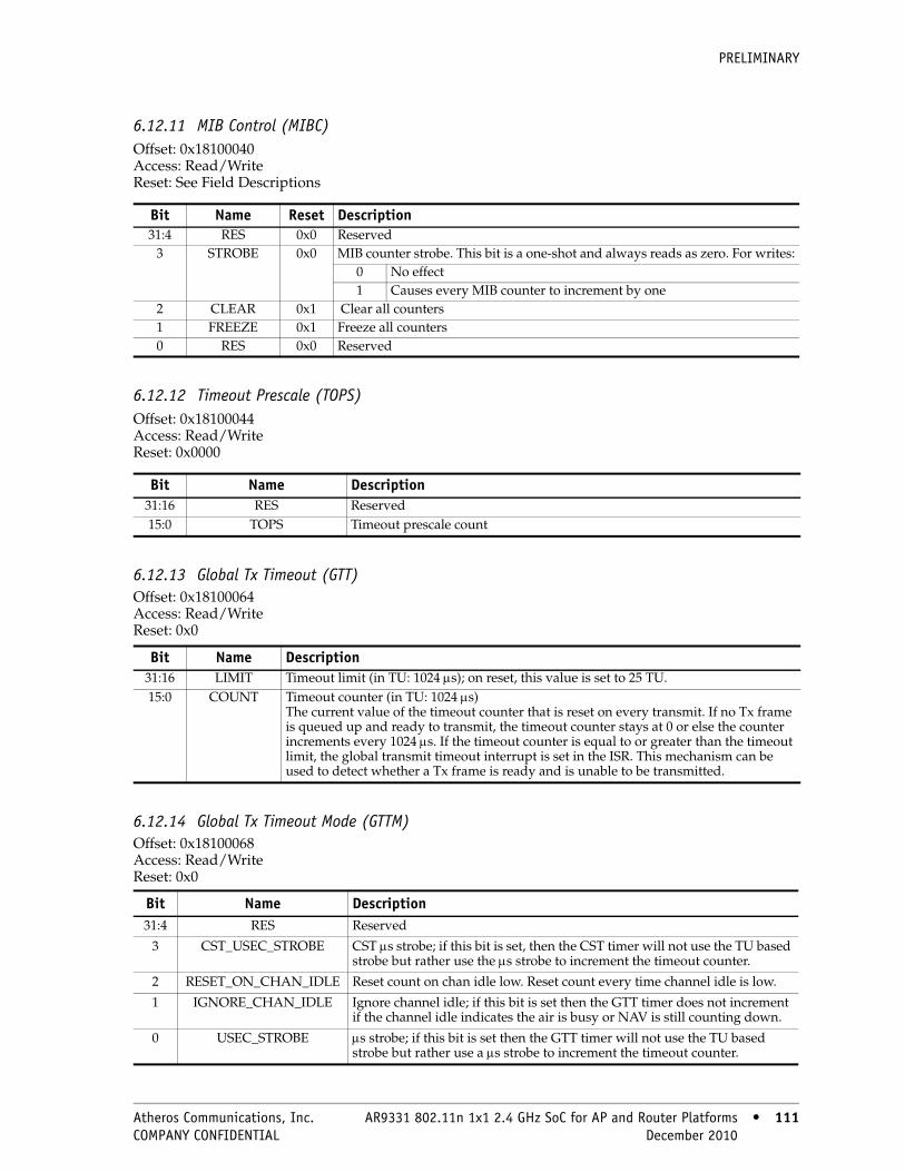
PRELIMINARY
6.12.11 MIB Control (MIBC)Offset: 0x18100040 Access: Read/Write Reset: See Field Descriptions
6.12.12 Timeout Prescale (TOPS)Offset: 0x18100044 Access: Read/Write Reset: 0x0000
6.12.13 Global Tx Timeout (GTT)Offset: 0x18100064 Access: Read/Write Reset: 0x0
6.12.14 Global Tx Timeout Mode (GTTM)Offset: 0x18100068 Access: Read/Write Reset: 0x0
Bit Name Reset Description31:4 RES 0x0 Reserved
3 STROBE 0x0 MIB counter strobe. This bit is a one-shot and always reads as zero. For writes:0 No effect1 Causes every MIB counter to increment by one
2 CLEAR 0x1 Clear all counters1 FREEZE 0x1 Freeze all counters0 RES 0x0 Reserved
Bit Name Description31:16 RES Reserved15:0 TOPS Timeout prescale count
Bit Name Description31:16 LIMIT Timeout limit (in TU: 1024 μs); on reset, this value is set to 25 TU.15:0 COUNT Timeout counter (in TU: 1024 μs)
The current value of the timeout counter that is reset on every transmit. If no Tx frame is queued up and ready to transmit, the timeout counter stays at 0 or else the counter increments every 1024 μs. If the timeout counter is equal to or greater than the timeout limit, the global transmit timeout interrupt is set in the ISR. This mechanism can be used to detect whether a Tx frame is ready and is unable to be transmitted.
Bit Name Description31:4 RES Reserved
3 CST_USEC_STROBE CST μs strobe; if this bit is set, then the CST timer will not use the TU based strobe but rather use the μs strobe to increment the timeout counter.
2 RESET_ON_CHAN_IDLE Reset count on chan idle low. Reset count every time channel idle is low.
1 IGNORE_CHAN_IDLE Ignore channel idle; if this bit is set then the GTT timer does not increment if the channel idle indicates the air is busy or NAV is still counting down.
0 USEC_STROBE μs strobe; if this bit is set then the GTT timer will not use the TU based strobe but rather use a μs strobe to increment the timeout counter.
Atheros Communications, Inc. AR9331 802.11n 1x1 2.4 GHz SoC for AP and Router Platforms • 111 COMPANY CONFIDENTIAL December 2010 • 111

PRELIMINARY
6.12.15 Carrier Sense Timeout (CST)Offset: 0x1810006C Access: Read/Write Reset: 0x0
6.12.16 Size of High and Low Priority (RXDP_SIZE)Offset: 0x18100070 Access: Read-Only Reset: 0x0
6.12.17 MAC Rx High Priority Queue RXDP Pointer (RX_QUEUE_HP_RXDP)Offset: 0x18100074 Access: Read/Write Reset: 0x0
6.12.18 MAC Rx Low Priority Queue RXDP Pointer (RX_QUEUE_LP_RXDP)Offset: 0x18100078 Access: Read/Write Reset: 0x0
Bit Name Description
31:16 LIMIT Timeout limit (in TU: 1024 μs). On reset, this value is set to 0 TU.
15:0 COUNT Timeout counter (in TU: 1024 μs) The current value of the timeout counter that is reset on every transmit. If no Tx frame is queued up and ready to transmit, the timeout counter stays at 0 or the counter increments every 1024 μs. If the timeout counter is equal to or greater than the timeout limit then carrier sense timeout (CST) interrupt is set in the ISR. This counter starts counting if any queues are ready for Tx. It continues counting when RX_CLEAR is low, which is useful to determine whether the transmit is stuck because RX_CLEAR is low for a long time.
Bit Name Description
31:13 RES Reserved
12:8 HP Indicates the size of high priority RXDP FIFO
7:0 LP Indicates the size of low priority RXDP FIFO
Bit Name Description
31:0 ADDR MAC Rx high priority queue RXDP pointer
Bit Name Description
31:0 ADDR MAC Rx low priority queue RXDP pointer
112 • AR9331 802.11n 1x1 2.4 GHz SoC for AP and Router Platforms Atheros Communications, Inc. 112 • December 2010 COMPANY CONFIDENTIAL

PRELIMINARY
6.12.19 Primary Interrupt Status (ISR_P)Offset: 0x18100080 Access: Read/Write-One-to-Clear Reset: 0x0
NOTE: ■ The bits that are logical ORs of bits in the
secondary ISRs are generated by logically ORing the secondary ISR bits after the secondary ISR bits have been masked with the appropriate bits from the corresponding secondary interrupt mask register.
■ A write of one to a bit that is a logical OR of bits in a secondary ISR clears the secondary ISR bits from which the primary ISR bit is generated. E.g.: A write of a one to the TXOK bit (bit [6]) in ISR_P clears all 10 TXOK bits in ISR_S0 (bits [9:0] of “Secondary Interrupt Status 0 (ISR_S0)”).
■ Only the bits in this register (ISR_P) and the primary interrupt mask register (“Primary Interrupt Mask (IMR_P)”) control whether the MAC’s interrupt output is asserted. The bits in the several secondary interrupt status/mask registers control what bits are set in the primary interrupt status register; however, the IMR_S* registers do not determine whether an interrupt is asserted. That is, an interrupt is asserted only when the logical AND of ISR_P and IMR_P is non-zero. The secondary interrupt mask/status registers affect which bits are set in ISR_P, but do not directly affect whether an interrupt is asserted.
Bit Name Description31 RXINTM Rx completion interrupt after mitigation; either the first Rx packet or last Rx packet
interrupt mitigation count has reached its threshold (see the register “Rx Interrupt Mitigation Thresholds (RIMT)” on page 109)
30 TXINTM Tx completion interrupt after mitigation; either the first Tx packet or last Tx packet interrupt mitigation count has reached its threshold (see the register “Tx Interrupt Mitigation Thresholds (TIMT)” on page 109)
29 RES Reserved28 GENTMR Logical OR of all GENERIC TIMER bits in the secondary ISR 5 which include the
GENERIC_TIMER_TRIGGER[7:0], GENERIC_TIMER_THRESH[7:0], GENERIC_TIMER_OVERFLOW
27 QTRIG Logical OR of all QTRIG bits in secondary ISR 4; indicates that at least one QCU's frame scheduling trigger event has occurred
26 QCBRURN Logical OR of all QCBRURN bits in secondary ISR 3; indicates that at least one QCU's frame scheduling trigger event occurred when no frames were present on the queue
25 QCBROVF Logical OR of all QCBROVF bits in secondary ISR 3; indicates that at least one QCU’s CBR expired counter has reached the value of the QCU’s CBR_OVR_THRESH parameter (see “CBR Configuration (Q_CBRCFG)” register bits [31:24])
24 RXMINTR RXMINTR maximum receive interrupt rate; same as RXINTM with the added requirement that maximum interrupt rate count has reached its threshold; this interrupt alternates with TXMINTR.
23 BCNMISC Miscellaneous beacon-related interrupts This bit is the Logical OR of the CST, GTT, TIM, CABEND, DTIMSYNC, BCNTO, CABTO, TSFOOR, DTIM, and TBTT_TIME bits in secondary ISR 2.
22:21 RES Reserved20 BNR Beacon not ready
Indicates that the QCU marked as being used for beacons received a DMA beacon alert when the queue contained no frames.
19 TXMINTR TXMINTR maximum Tx interrupt rate18 BMISS The PCU indicates that is has not received a beacon during the previous N (N is
programmable) beacon periods17 BRSSI The PCU indicates that the RSSI of a beacon it has received has fallen below a
programmable threshold16 SWBA The PCU has signalled a software beacon alert15 RXKCM Key cache miss; a frame was received with a set key cache miss Rx status bit14 RXPHY The PHY signalled an error on a received frame
Atheros Communications, Inc. AR9331 802.11n 1x1 2.4 GHz SoC for AP and Router Platforms • 113 COMPANY CONFIDENTIAL December 2010 • 113

PRELIMINARY
6.12.20 Secondary Interrupt Status 0 (ISR_S0)Offset: 0x18100084 Access: Read/Write-One-to-Clear Reset: 0x0
6.12.21 Secondary Interrupt Status 1 (ISR_S1)Offset: 0x18100088 Access: Read/Write-One-to-Clear Reset: 0x0
13 SWI Software interrupt signalled; see the register “Command (CR)” on page 10612 MIB One of the MIB regs has reached its threshold11 TXURN Logical OR of all TXURN bits in secondary ISR 2. Indicates that the PCU reported a
txfifo underrun for at least one QCU’s frame10 TXEOL Logical OR of all TXEOL bits in secondary ISR 1; indicates that at least one Tx desc
fetch state machine has no more Tx descs available9 RES Reserved8 TXERR Logical OR of all TXERR bits in secondary ISR 1; indicates that at least one frame was
completed with an error, regardless of whether the InterReq bit was set7 RES Reserved6 TXOK Logical OR of all TXOK bits in secondary ISR 0; indicates that at least one frame was
completed with no errors and at the requested rate, regardless of whether the InterReq bit was set.
5 RXORN RxFIFO overrrun4 RXEOL Rx descriptor fetch logic has no more Rx descs available3 RXNOFR No frame was received for RXNOFR timeout clocks2 RXERR The frame was received with errors1 RXOK_LP Low priority frame was received with no errors0 RXOK_HP High priority frame was received with no errors
Bit Name Description
Bit Description31:10 Reserved
9 TXOK for QCU 9... ...1 TXOK for QCU 10 TXOK for QCU 0
Bit Description31:26 Reserved
25 TXEOL for QCU 9... ...17 TXEOL for QCU 116 TXEOL for QCU 0
15:10 Reserved9 TXERR for QCU 9... ...1 TXERR for QCU 10 TXERR for QCU 0
114 • AR9331 802.11n 1x1 2.4 GHz SoC for AP and Router Platforms Atheros Communications, Inc. 114 • December 2010 COMPANY CONFIDENTIAL
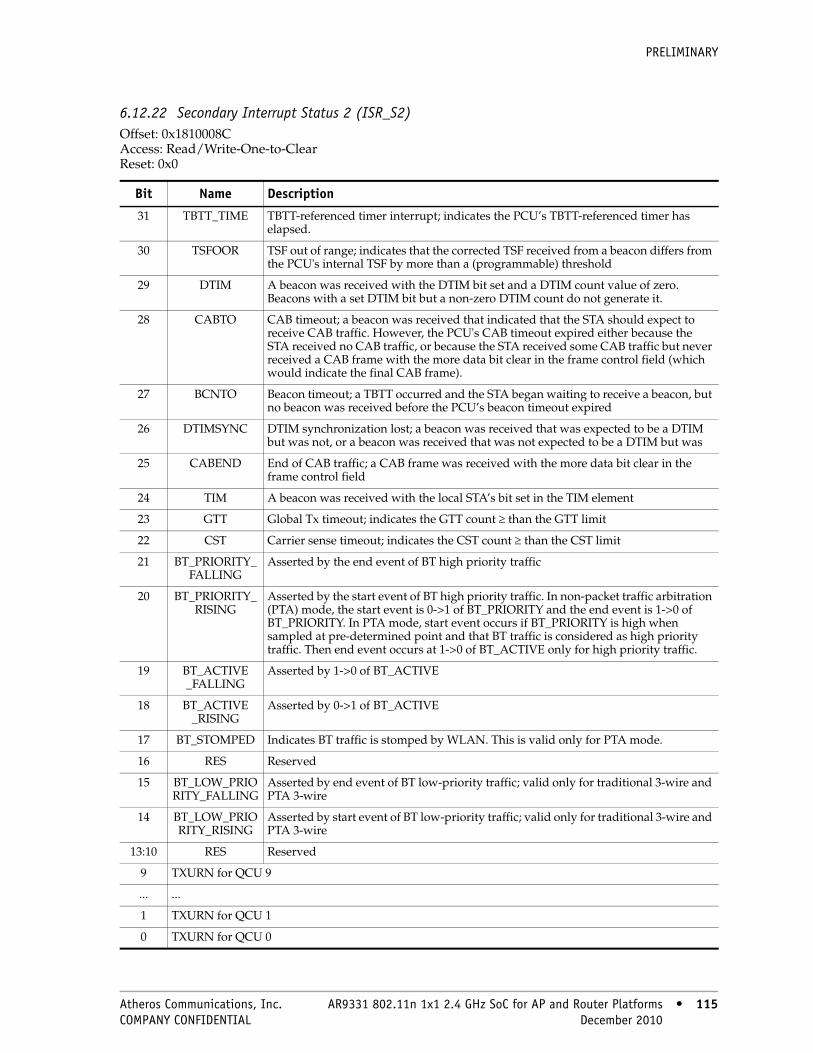
PRELIMINARY
6.12.22 Secondary Interrupt Status 2 (ISR_S2)Offset: 0x1810008C Access: Read/Write-One-to-Clear Reset: 0x0
Bit Name Description
31 TBTT_TIME TBTT-referenced timer interrupt; indicates the PCU’s TBTT-referenced timer has elapsed.
30 TSFOOR TSF out of range; indicates that the corrected TSF received from a beacon differs from the PCU's internal TSF by more than a (programmable) threshold
29 DTIM A beacon was received with the DTIM bit set and a DTIM count value of zero. Beacons with a set DTIM bit but a non-zero DTIM count do not generate it.
28 CABTO CAB timeout; a beacon was received that indicated that the STA should expect to receive CAB traffic. However, the PCU's CAB timeout expired either because the STA received no CAB traffic, or because the STA received some CAB traffic but never received a CAB frame with the more data bit clear in the frame control field (which would indicate the final CAB frame).
27 BCNTO Beacon timeout; a TBTT occurred and the STA began waiting to receive a beacon, but no beacon was received before the PCU’s beacon timeout expired
26 DTIMSYNC DTIM synchronization lost; a beacon was received that was expected to be a DTIM but was not, or a beacon was received that was not expected to be a DTIM but was
25 CABEND End of CAB traffic; a CAB frame was received with the more data bit clear in the frame control field
24 TIM A beacon was received with the local STA’s bit set in the TIM element
23 GTT Global Tx timeout; indicates the GTT count ≥ than the GTT limit
22 CST Carrier sense timeout; indicates the CST count ≥ than the CST limit
21 BT_PRIORITY_FALLING
Asserted by the end event of BT high priority traffic
20 BT_PRIORITY_RISING
Asserted by the start event of BT high priority traffic. In non-packet traffic arbitration (PTA) mode, the start event is 0->1 of BT_PRIORITY and the end event is 1->0 of BT_PRIORITY. In PTA mode, start event occurs if BT_PRIORITY is high when sampled at pre-determined point and that BT traffic is considered as high priority traffic. Then end event occurs at 1->0 of BT_ACTIVE only for high priority traffic.
19 BT_ACTIVE_FALLING
Asserted by 1->0 of BT_ACTIVE
18 BT_ACTIVE_RISING
Asserted by 0->1 of BT_ACTIVE
17 BT_STOMPED Indicates BT traffic is stomped by WLAN. This is valid only for PTA mode.
16 RES Reserved
15 BT_LOW_PRIORITY_FALLING
Asserted by end event of BT low-priority traffic; valid only for traditional 3-wire and PTA 3-wire
14 BT_LOW_PRIORITY_RISING
Asserted by start event of BT low-priority traffic; valid only for traditional 3-wire and PTA 3-wire
13:10 RES Reserved
9 TXURN for QCU 9
... ...
1 TXURN for QCU 1
0 TXURN for QCU 0
Atheros Communications, Inc. AR9331 802.11n 1x1 2.4 GHz SoC for AP and Router Platforms • 115 COMPANY CONFIDENTIAL December 2010 • 115

PRELIMINARY
6.12.23 Secondary Interrupt Status 3 (ISR_S3)Offset: 0x18100090 Access: Read/Write-One-to-Clear Reset: 0x0
6.12.24 Secondary Interrupt Status 4 (ISR_S4)Offset: 0x18100094 Access: Read/Write-One-to-Clear Reset: 0x0
6.12.25 Secondary Interrupt Status 5 (ISR_S5)Offset: 0x18100098 Access: Read/Write-One-to-Clear Reset: 0x0
NOTE: The trigger indicates that the TSF matched or exceeded the timer. The threshold is set when the TSF exceeds the timer by the GENERIC_TIMER_THRESH value. The GENERIC_TIMER overflow occurs when the TSF exceeds the timer by such a large amount that TSF ≥ Timer + Period, indicating incorrect software programming. The GENERIC_TIMER 0 threshold was removed because timer 0 is special and does not generate threshold event.
Bit Description31:26 Reserved
25 QCBRURN for QCU 9... ...17 QCBRURN for QCU 116 QCBRURN for QCU 0
15:10 Reserved9 QCBROVF for QCU 91 QCBROVF for QCU 1... ...0 QCBROVF for QCU 0
Bit Description31:10 Reserved
9 QTRIG for QCU 9... ...1 QTRIG for QCU 10 QTRIG for QCU 0
Bit Description31 GENERIC_TIMER 15 threshold... ...17 GENERIC_TIMER 1 threshold16 GENERIC_TIMER overflow15 GENERIC_TIMER 15 trigger... ...1 GENERIC_TIMER 1 trigger0 GENERIC_TIMER 0 trigger
116 • AR9331 802.11n 1x1 2.4 GHz SoC for AP and Router Platforms Atheros Communications, Inc. 116 • December 2010 COMPANY CONFIDENTIAL

PRELIMINARY
6.12.26 Primary Interrupt Mask (IMR_P)Offset: 0x181000A0 Access: Read/Write Reset: 0x0
NOTE: Only the bits in this register control whether the MAC’s interrupt outputs are asserted. The bits in the secondary interrupt mask registers control what bits are set in the “Primary Interrupt Mask (IMR_P)” register; however, the IMR_S* registers do not determine whether an interrupt is asserted.
Bit Description
31 RXINTM interrupt enable
30 TXINTM interrupt enable
29 Reserved
28 GENTMR interrupt enable
27 QTRIG interrupt enable
26 QCBRURN interrupt enable
25 QCBROVF interrupt enable
24 RXMINTR interrupt enable
23 BCNMISC interrupt enable
22:21 Reserved
20 BNR interrupt enable
19 TXMINTR interrupt enable
18 BMISS interrupt enable
17 BRSSI interrupt enable
16 SWBA interrupt enable
15 RXKCM interrupt enable
14 RXPHY interrupt enable
13 SWI interrupt enable
12 MIB interrupt enable
11 TXURN interrupt enable
10 TXEOL interrupt enable
9 TXNOFR interrupt enable
8 TXERR interrupt enable
7 Reserved
6 TXOK interrupt enable
5 RXORN interrupt enable
4 RXEOL interrupt enable
3 RXNOFR interrupt enable
2 RXERR interrupt enable
1 RXOK_LP interrupt enable
0 RXOK_HP interrupt enable
Atheros Communications, Inc. AR9331 802.11n 1x1 2.4 GHz SoC for AP and Router Platforms • 117 COMPANY CONFIDENTIAL December 2010 • 117

PRELIMINARY
6.12.27 Secondary Interrupt Mask 0 (IMR_S0)Offset: 0x181000A4 Access: Read/Write Reset: 0x0
6.12.28 Secondary Interrupt Mask 1 (IMR_S1)Offset: 0x181000A8 Access: Read/Write Reset: 0x0
Bit Description
31:10 Reserved
9 TXOK for QCU 9 interrupt enable
... ...
1 TXOK for QCU 1 interrupt enable
0 TXOK for QCU 0 interrupt enable
Bit Description
31:26 Reserved
25 TXEOL for QCU 9 interrupt enable
... ...
17 TXEOL for QCU 1 interrupt enable
16 TXEOL for QCU 0 interrupt enable
15:10 Reserved
9 TXERR for QCU 9 interrupt enable
... ...
1 TXERR for QCU 1 interrupt enable
0 TXERR for QCU 0 interrupt enable
118 • AR9331 802.11n 1x1 2.4 GHz SoC for AP and Router Platforms Atheros Communications, Inc. 118 • December 2010 COMPANY CONFIDENTIAL
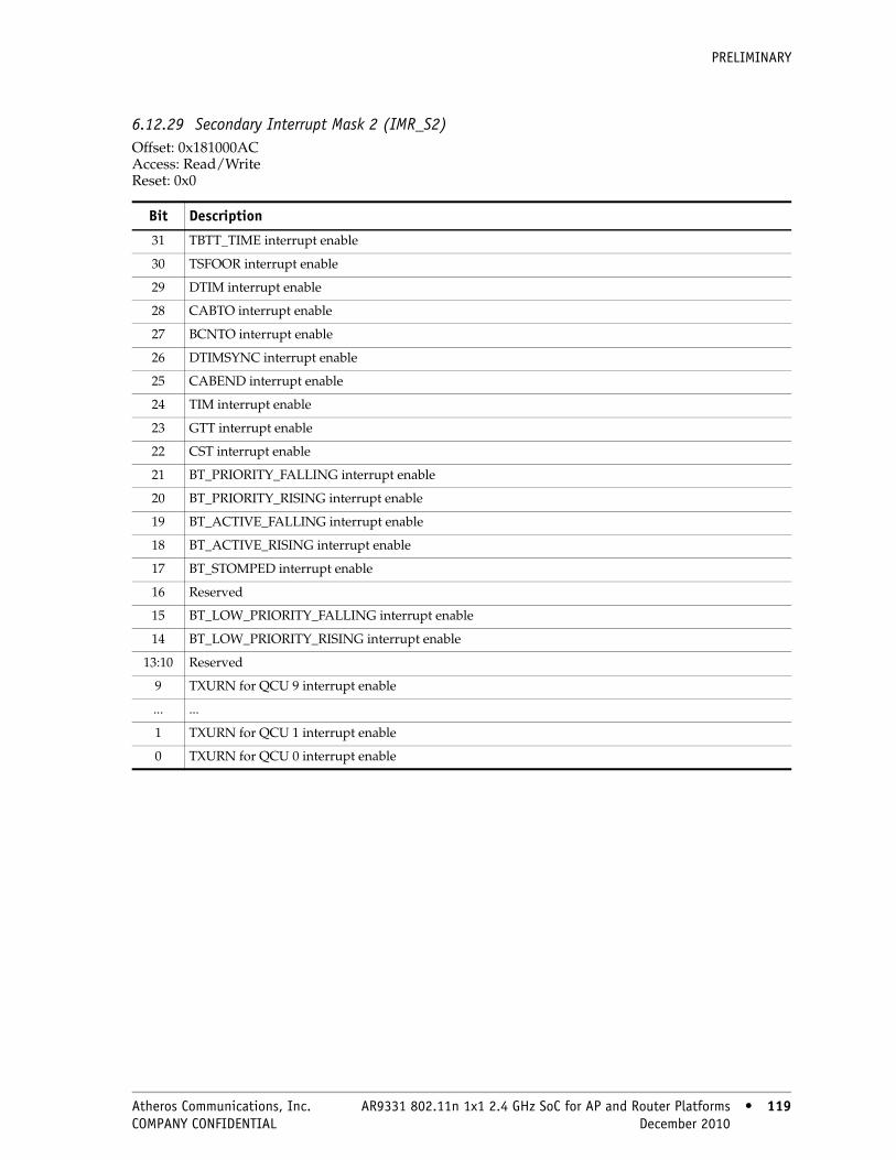
PRELIMINARY
6.12.29 Secondary Interrupt Mask 2 (IMR_S2)Offset: 0x181000AC Access: Read/Write Reset: 0x0
Bit Description
31 TBTT_TIME interrupt enable
30 TSFOOR interrupt enable
29 DTIM interrupt enable
28 CABTO interrupt enable
27 BCNTO interrupt enable
26 DTIMSYNC interrupt enable
25 CABEND interrupt enable
24 TIM interrupt enable
23 GTT interrupt enable
22 CST interrupt enable
21 BT_PRIORITY_FALLING interrupt enable
20 BT_PRIORITY_RISING interrupt enable
19 BT_ACTIVE_FALLING interrupt enable
18 BT_ACTIVE_RISING interrupt enable
17 BT_STOMPED interrupt enable
16 Reserved
15 BT_LOW_PRIORITY_FALLING interrupt enable
14 BT_LOW_PRIORITY_RISING interrupt enable
13:10 Reserved
9 TXURN for QCU 9 interrupt enable
... ...
1 TXURN for QCU 1 interrupt enable
0 TXURN for QCU 0 interrupt enable
Atheros Communications, Inc. AR9331 802.11n 1x1 2.4 GHz SoC for AP and Router Platforms • 119 COMPANY CONFIDENTIAL December 2010 • 119
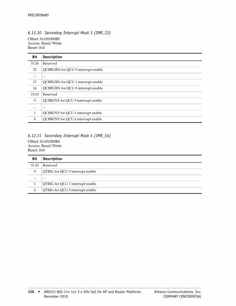
PRELIMINARY
6.12.30 Secondary Interrupt Mask 3 (IMR_S3)Offset: 0x181000B0 Access: Read/Write Reset: 0x0
6.12.31 Secondary Interrupt Mask 4 (IMR_S4)Offset: 0x181000B4 Access: Read/Write Reset: 0x0
Bit Description
31:26 Reserved
25 QCBRURN for QCU 9 interrupt enable
... ...
17 QCBRURN for QCU 1 interrupt enable
16 QCBRURN for QCU 0 interrupt enable
15:10 Reserved
9 QCBROVF for QCU 9 interrupt enable
... ...
1 QCBROVF for QCU 1 interrupt enable
0 QCBROVF for QCU 0 interrupt enable
Bit Description
31:10 Reserved
9 QTRIG for QCU 9 interrupt enable
... ...
1 QTRIG for QCU 1 interrupt enable
0 QTRIG for QCU 0 interrupt enable
120 • AR9331 802.11n 1x1 2.4 GHz SoC for AP and Router Platforms Atheros Communications, Inc. 120 • December 2010 COMPANY CONFIDENTIAL
PRELIMINARY
6.12.32 Secondary Interrupt Mask 5 (IMR_S5)Offset: 0x181000B8 Access: Read/Write-One-to-Clear Reset: 0x0
NOTE: The trigger indicates the TSF matched or exceeded the timer; threshold is set when the TSF exceeds the timer by the GENERIC_TIMER_THRESH value. The GENERIC_TIMER overflow occurs when the TSF exceeds the timer by such a large amount that TSF ≥ Timer + Period, indicating incorrect software programming. The threshold GENERIC_TIMER 0 was removed because timer 0 is special and does not generate a threshold event.
6.12.33 Primary Interrupt Status Read and Clear (ISR_P_RAC)Offset: 0x181000C0 Access: Read-and-Clear (No Write Access) Reset: 0x0
NOTE: A read from this location atomically:
■ Copies all secondary ISRs into the corresponding secondary ISR shadow registers (ISR_S0 is copied to ISR_S0_S, etc.)
■ Clears all bits of the primary ISR (ISR_P) and all bits of all secondary ISRs (ISR_S0–ISR_S4)
■ Returns the contents of the primary ISR (ISR_P)
6.12.34 Secondary Interrupt Status 0 (ISR_S0_S)Offset: 0x181000C4 Access: Read-Only Reset: 0x0
Bit Description
31 GENERIC_TIMER_THRESHOLD 15
30 GENERIC_TIMER_THRESHOLD 14
... ...
18 GENERIC_TIMER_THRESHOLD 2
17 GENERIC_TIMER_THRESHOLD 1
16 GENERIC_TIMER overflow enable
15 GENERIC_TIMER 15 trigger enable
... ...
1 GENERIC_TIMER 1 trigger enable
0 GENERIC_TIMER 0 trigger enable
Bit Name Description
31:0 ISR_P Same format as “Primary Interrupt Status (ISR_P)”
Bit Name Description
31:0 ISR_S0 Same format as “Secondary Interrupt Status 0 (ISR_S0)”
Atheros Communications, Inc. AR9331 802.11n 1x1 2.4 GHz SoC for AP and Router Platforms • 121 COMPANY CONFIDENTIAL December 2010 • 121

PRELIMINARY
6.12.35 Secondary Interrupt Status 1 (ISR_S1_S)Offset: 0x181000C8 Access: Read-Only Reset: 0x0
6.12.36 Secondary Interrupt Status 2 (ISR_S2_S)Offset: 0x181000D0 Access: Read-Only Reset: 0x0
6.12.37 Secondary Interrupt Status 3 (ISR_S3_S)Offset: 0x181000D4 Access: Read-Only Reset: 0x0
6.12.38 Secondary Interrupt Status 4 (ISR_S4_S)Offset: 0x181000D8 Access: Read-Only Reset: 0x0
6.12.39 Secondary Interrupt Status 5 (ISR_S5_S)Offset: 0x181000DC Access: Read-Only Reset: 0x0
Bit Name Description
31:0 ISR_S0 Same format as “Secondary Interrupt Status 1 (ISR_S1)”
Bit Name Description
31:0 ISR_S0 Same format as “Secondary Interrupt Status 2 (ISR_S2)”
Bit Name Description
31:0 ISR_S0 Same format as “Secondary Interrupt Status 3 (ISR_S3)”
Bit Name Description
31:0 ISR_S0 Same format as “Secondary Interrupt Status 4 (ISR_S4)”
Bit Name Description
31:0 ISR_S0 Same format as “Secondary Interrupt Status 5 (ISR_S5)”
122 • AR9331 802.11n 1x1 2.4 GHz SoC for AP and Router Platforms Atheros Communications, Inc. 122 • December 2010 COMPANY CONFIDENTIAL

PRELIMINARY
Beacon Handling
Table 6-4. AP in a BSS: Sending Beacon and CAB
QCU Description
QCU 9 QCU 9 is used only for beaconsQCU 9 feeds into DCU 9, and is the only QCU to feed into DCU 9
For QCU 9 For DCU 9
1. Set FSP to DBA-gated (see bits [3:0] of “Misc. QCU Settings (Q_MISC)”).
2. Set the bit so the QCU sends beacons (Q_MISC bit [7]).
3. Set the bit to disable CBRExpired counter increment if the local queue has no frames (Q_MISC bit [5]).
1. Set the bit so DCU sends beacons (bit [16] of “Misc. DCU-Specific Settings (D_MISC)”).
2. Set the bit to enable global lockout (set D_MISC bits [18:17] to 0x2).
3. Set both CW_MIN and CW_MAX to zero (see “DCU-Specific IFS Settings (D_LCL_IFS)”).
QCU 8 QCU 8 is used only for CAB (for a BSS, CAB is BCAST and MCAST frames)QCU 8 feeds into DCU 8, and is the only QCU to feed into DCU 8
For QCU 8 For DCU 8
1. Set FSP to DBA-gate
2. Set the ReadyTimeEn bit and set the ReadyTimeDuration (RTD) to:
RTD = BeaconInterval – (SBA – DBA)■ BeaconInterval is the interval between TBTTs■ SBA is the amount of time before TBTT that
SBA is generated■ DBA is the amount of time before TBTT that
DBA is generated
3. Set the bit to disable the CBRExpired counter increment if the beacon queue has no frames (bit [6] of “Misc. QCU Settings (Q_MISC)”).
4. Set the bit to disable the CBRExpired counter increment if the local queue has no frames (Q_MISC bit [5]).
1. Set the bit to enable global lockout.
2. Software tasks at SBA (all of these must occur before DBA):
■ Build beacon and pass it to QCU 9.
■ Build CAB and pass it to QCU 8.
■ Clear all Tx filter bits for DCUs 9 and 8.
Atheros Communications, Inc. AR9331 802.11n 1x1 2.4 GHz SoC for AP and Router Platforms • 123 COMPANY CONFIDENTIAL December 2010 • 123
PRELIMINARY
Table 6-5. STA in an IBSS: Sending Beacon and CAB
QCU Description
QCU 9 QCU 9 is used only for beacons; QCU 9 feeds into DCU 9, and is the only QCU to feed into DCU 9
For QCU 9 For DCU 9
1. Set FSP to DBA-gated (Q_MISC bits [3:0]).
2. Set the bit so the QCU sends beacons (Q_MISC bit [7]).
1. Set DCU to send beacons (D_MISC bit [16]).
2. Set the bit to enable global lockout (set D_MISC bits [18:17] to 0x2).
3. Set both CW_MIN and CW_MAX to twice the usual CW_MIN value (refer to the 802.11 specifications).
QCU 8 QCU 8 is used only for CAB (for an IBSS, CAB is ATIMs followed by data frames requiring preceding ATIM reception); QCU 8 feeds into DCU 8, and is the only QCU to feed into DCU 8
For QCU 8 For DCU 8
1. Set FSP to DBA-gate
2. Set the ReadyTimeEn bit and set the ReadyTimeDuration (RTD) to:
RTD = BeaconInterval – (SBA – DBA)3. Set the bit to disable the CBRExpired counter
increment if the beacon queue has no frames (bit [6] of “Misc. QCU Settings (Q_MISC)”).
4. Set the bit to disable the CBRExpired counter increment if the beacon queue has no frames (Q_MISC bit [6]).
5. Set the bit to disable the CBRExpired counter increment if the local queue has no frames (Q_MISC bit [5]).
6. Set the bit to clear TXE if ReadyTime expires (Q_MISC bit [9]).
1. Set the bit to enable global lockout.
2. Software tasks at SBA (all of these must occur before DBA):
■ Build beacon and pass it to QCU 9.
■ Build CAB and pass it to QCU 8.
■ Clear all Tx filter bits for DCUs 9 and 8.
124 • AR9331 802.11n 1x1 2.4 GHz SoC for AP and Router Platforms Atheros Communications, Inc. 124 • December 2010 COMPANY CONFIDENTIAL

PRELIMINARY
6.13 QCU RegistersThe QCU registers occupy the offset range 0x18100800– 0x18100A40 in the AR9331 address space. The AR9331 has ten QCUs, numbered from 0 to 9.
6.13.1 Tx Queue Descriptor (Q_TXDP)Offset: 0x18100800 + (Q < 2) Access: Read/Write Cold Reset: Undefined Warm Reset: Unaffected
Table 6-7. QCU Registers
Offset Name Description Page
0x18100800 + (Q << 2)[1] Q_TXDP Tx Queue Descriptor Pointer page 125
0x18100830 Q_STATUS_RING_START QCU_STATUS_RING_START_ ADDRESS Lower 32 bits of Address
page 126
0x18100834 Q_STATUS_RING_END QCU_STATUS_RING_END_ADDR Lower 32 Bits of Address
page 126
0x18100838 Q_STATUS_RING_CURRENT QCU_STATUS_RING_CURRENT Address
page 126
0x18100840 Q_TXE Tx Queue Enable page 126
0x18100880 Q_TXD Tx Queue Disable page 127
0x181008C0 + (Q << 2)[1] Q_CBRCFG CBR Configuration page 127
0x18100900 + (Q << 2)[1] Q_RDYTIMECFG ReadyTime Configuration page 127
0x18100940 Q_ONESHOTARM_SC OneShotArm Set Control page 128
0x18100980 Q_ONESHOTARM_CC OneShotArm Clear Control page 128
0x181009C0 + (Q << 2)[1] Q_MISC Miscellaneous QCU Settings page 129
0x18100A00 + (Q << 2)[1] Q_STS Miscellaneous QCU Status page 131
0x18100A40 Q_RDYTIMESHDN ReadyTimeShutdown Status page 131
0x18100A44 Q_MAC_QCU_DESC_CRC_CHK Descriptor CRC Check page 131
[1]The variable Q in the register addresses refers to the QCU number.
Bit Name Description
31:2 TXDP Tx descriptor pointer
1:0 RES Reserved
Atheros Communications, Inc. AR9331 802.11n 1x1 2.4 GHz SoC for AP and Router Platforms • 125 COMPANY CONFIDENTIAL December 2010 • 125
PRELIMINARY
6.13.2 QCU_STATUS_RING_START_ADDRESS Lower 32 bits of Address (Q_STATUS_RING_START)Offset: 0x18100830 Access: Read/Write Reset: 0x0
6.13.3 QCU_STATUS_RING_END_ADDR Lower 32 Bits of Address (Q_STATUS_RING_END)Offset: 0x18100834 Access: Read/Write Reset: 0x0
6.13.4 QCU_STATUS_RING_CURRENT Address (Q_STATUS_RING_CURRENT)Offset: 0x18100838 Access: Read/Write Reset: 0x0
6.13.5 Tx Queue Enable (Q_TXE)Offset: 0x18100840 Access: Read/Write Reset: 0x0
NOTE: Writing a 1 in bit position N sets the TXE bit for QCU N. Writing a 0 in bit position N has no effect; in particular, it does not clear the TXE bit for the QCU.
Bit Name Description
31:0 ADDR Lower 32 bits of QCU_STATUS_RING_START_ADDR
Bit Name Description
31:0 ADDR Lower 32 bits of QCU_STATUS_RING_END_ADDR
Bit Name Description
31:0 ADDR MAC_QCU_STATUS_RING_CURRENT_ADDRESS
Bit Description
31:10 Reserved
9 Enable QCU 9
... ...
1 Enable QCU 1
0 Enable QCU 0
126 • AR9331 802.11n 1x1 2.4 GHz SoC for AP and Router Platforms Atheros Communications, Inc. 126 • December 2010 COMPANY CONFIDENTIAL

PRELIMINARY
6.13.6 Tx Queue Disable (Q_TXD)Offset: 0x18100880 Access: Read/Write Reset: 0x0
NOTE: To stop transmission for QCU Q:
1. Write a 1 to QCU Q's TXD bit2. Poll the “Tx Queue Enable (Q_TXE)”
register until QCU Q’s TXE bit is clear3. Poll QCU Q’s “Misc. QCU Status (Q_STS)”
register until its pending frame count (Q_STS bits [1:0]) is zero
4. Write a 0 to QCU Q’s TXD bit
At this point, QCU Q has shut down and has no frames pending in its associated DCU.
Software must not write a 1 to a QCU’s TXE bit when that QCU's TXD bit is set; an undefined operation will result. Software must ensure that it sets a QCU’s TXE bit only when the QCU’s TXD bit is clear. It is fine to write a 0 to TXE when TXD is set, but this has no effect on the QCU.
6.13.7 CBR Configuration (Q_CBRCFG)Offset: 0x181008C0 + (Q < 2) Access: Read/Write Reset: 0x0
6.13.8 ReadyTime Configuration (Q_RDYTIMECFG)Offset: 0x18100900 + (Q < 2) Access: Read/Write Reset: 0x0
Bit Description
31:10 Reserved
9 Enable QCU 9
... ...
1 Enable QCU 1
0 Enable QCU 0
Bit Name Description
31:24 CBR_OVF_THRESH CBR overflow threshold
23:0 CBR_INTV CBR interval in μs
Bit Name Description
31:25 RES Reserved
24 RDYTIME_EN ReadyTime enable
0 Disable ReadyTime use
1 Enable ReadyTime use
23:0 RDYTIME_DUR ReadyTime duration in μs
Atheros Communications, Inc. AR9331 802.11n 1x1 2.4 GHz SoC for AP and Router Platforms • 127 COMPANY CONFIDENTIAL December 2010 • 127
PRELIMINARY
6.13.9 OneShotArm Set Control (Q_ONESHOTARM_SC)Offset: 0x18100940 Access: Read/Write Reset: 0x0
NOTE: A read to this register returns the current state of all OneShotArm bits (QCU Q’s OneShotArm bit is returned in bit position Q).
6.13.10 OneShotArm Clear Control (Q_ONESHOTARM_CC)Offset: 0x18100980 Access: Read/Write Reset: 0x0
NOTE: A read to this register returns the current state of all OneShotArm bits (QCU Q’s OneShotArm bit is returned in bit position Q).
Bit Description
31:10 Reserved
9 0 No effect
1 Set OneShot arm bit for QCU 9
... ...
1 0 No effect
1 Set OneShot arm bit for QCU 1
0 0 No effect
1 Set OneShot arm bit for QCU 0
Bit Description
31:10 Reserved
9 0 No effect
1 Clear OneShot arm bit for QCU 9
... ...
1 0 No effect
1 Clear OneShot arm bit for QCU 1
0 0 No effect
1 Clear OneShot arm bit for QCU 0
128 • AR9331 802.11n 1x1 2.4 GHz SoC for AP and Router Platforms Atheros Communications, Inc. 128 • December 2010 COMPANY CONFIDENTIAL
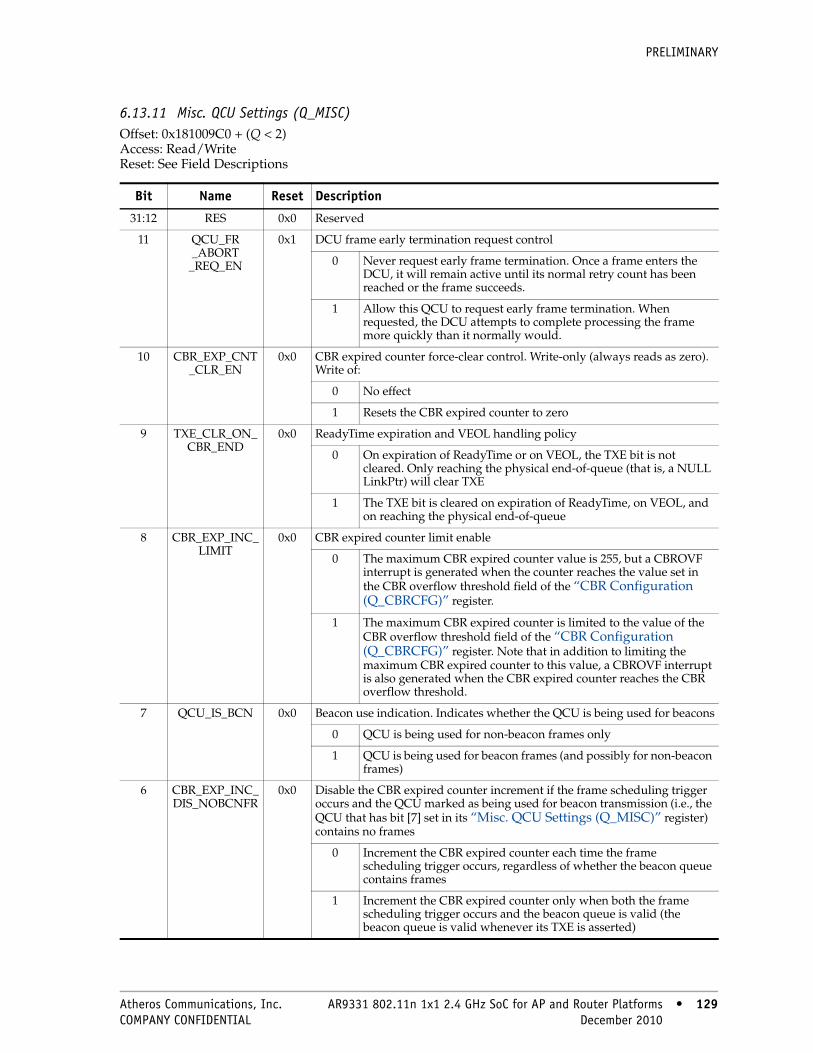
PRELIMINARY
6.13.11 Misc. QCU Settings (Q_MISC)Offset: 0x181009C0 + (Q < 2) Access: Read/Write Reset: See Field Descriptions
Bit Name Reset Description
31:12 RES 0x0 Reserved
11 QCU_FR_ABORT
_REQ_EN
0x1 DCU frame early termination request control
0 Never request early frame termination. Once a frame enters the DCU, it will remain active until its normal retry count has been reached or the frame succeeds.
1 Allow this QCU to request early frame termination. When requested, the DCU attempts to complete processing the frame more quickly than it normally would.
10 CBR_EXP_CNT_CLR_EN
0x0 CBR expired counter force-clear control. Write-only (always reads as zero). Write of:
0 No effect
1 Resets the CBR expired counter to zero
9 TXE_CLR_ON_CBR_END
0x0 ReadyTime expiration and VEOL handling policy
0 On expiration of ReadyTime or on VEOL, the TXE bit is not cleared. Only reaching the physical end-of-queue (that is, a NULL LinkPtr) will clear TXE
1 The TXE bit is cleared on expiration of ReadyTime, on VEOL, and on reaching the physical end-of-queue
8 CBR_EXP_INC_LIMIT
0x0 CBR expired counter limit enable
0 The maximum CBR expired counter value is 255, but a CBROVF interrupt is generated when the counter reaches the value set in the CBR overflow threshold field of the “CBR Configuration (Q_CBRCFG)” register.
1 The maximum CBR expired counter is limited to the value of the CBR overflow threshold field of the “CBR Configuration (Q_CBRCFG)” register. Note that in addition to limiting the maximum CBR expired counter to this value, a CBROVF interrupt is also generated when the CBR expired counter reaches the CBR overflow threshold.
7 QCU_IS_BCN 0x0 Beacon use indication. Indicates whether the QCU is being used for beacons
0 QCU is being used for non-beacon frames only
1 QCU is being used for beacon frames (and possibly for non-beacon frames)
6 CBR_EXP_INC_DIS_NOBCNFR
0x0 Disable the CBR expired counter increment if the frame scheduling trigger occurs and the QCU marked as being used for beacon transmission (i.e., the QCU that has bit [7] set in its “Misc. QCU Settings (Q_MISC)” register) contains no frames
0 Increment the CBR expired counter each time the frame scheduling trigger occurs, regardless of whether the beacon queue contains frames
1 Increment the CBR expired counter only when both the frame scheduling trigger occurs and the beacon queue is valid (the beacon queue is valid whenever its TXE is asserted)
Atheros Communications, Inc. AR9331 802.11n 1x1 2.4 GHz SoC for AP and Router Platforms • 129 COMPANY CONFIDENTIAL December 2010 • 129
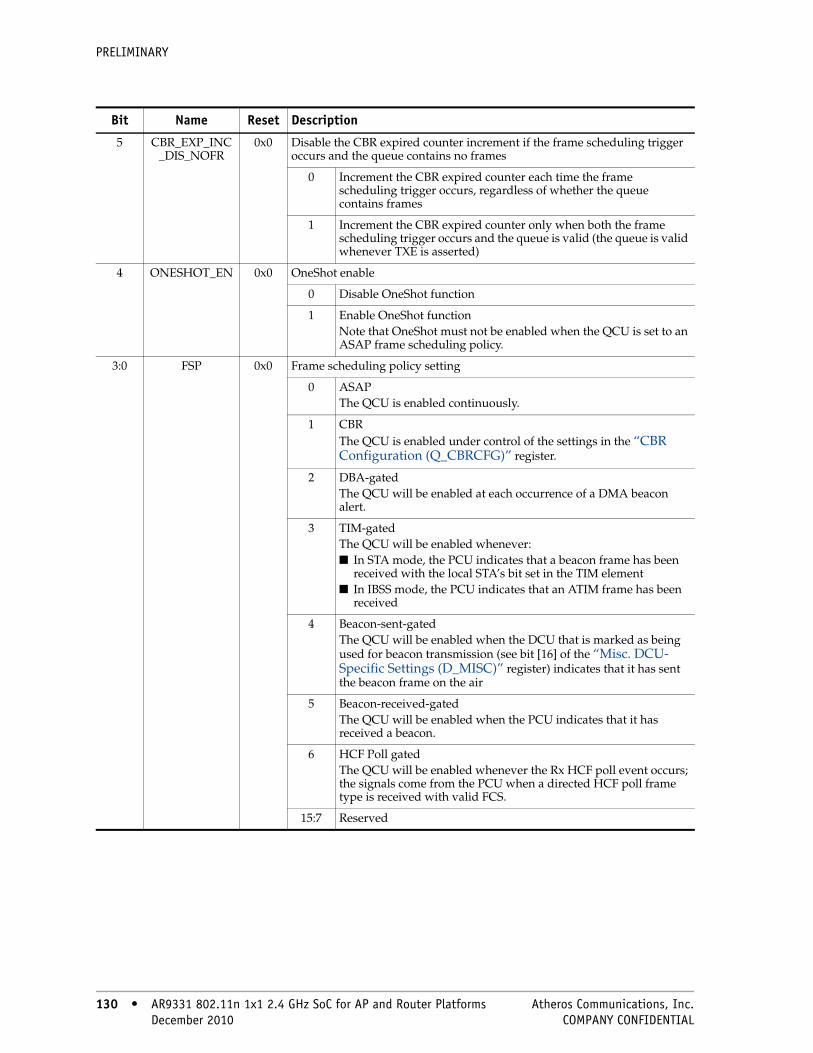
PRELIMINARY
5 CBR_EXP_INC_DIS_NOFR
0x0 Disable the CBR expired counter increment if the frame scheduling trigger occurs and the queue contains no frames
0 Increment the CBR expired counter each time the frame scheduling trigger occurs, regardless of whether the queue contains frames
1 Increment the CBR expired counter only when both the frame scheduling trigger occurs and the queue is valid (the queue is valid whenever TXE is asserted)
4 ONESHOT_EN 0x0 OneShot enable
0 Disable OneShot function
1 Enable OneShot functionNote that OneShot must not be enabled when the QCU is set to an ASAP frame scheduling policy.
3:0 FSP 0x0 Frame scheduling policy setting
0 ASAPThe QCU is enabled continuously.
1 CBRThe QCU is enabled under control of the settings in the “CBR Configuration (Q_CBRCFG)” register.
2 DBA-gatedThe QCU will be enabled at each occurrence of a DMA beacon alert.
3 TIM-gatedThe QCU will be enabled whenever:■ In STA mode, the PCU indicates that a beacon frame has been
received with the local STA’s bit set in the TIM element■ In IBSS mode, the PCU indicates that an ATIM frame has been
received
4 Beacon-sent-gatedThe QCU will be enabled when the DCU that is marked as being used for beacon transmission (see bit [16] of the “Misc. DCU-Specific Settings (D_MISC)” register) indicates that it has sent the beacon frame on the air
5 Beacon-received-gatedThe QCU will be enabled when the PCU indicates that it has received a beacon.
6 HCF Poll gatedThe QCU will be enabled whenever the Rx HCF poll event occurs; the signals come from the PCU when a directed HCF poll frame type is received with valid FCS.
15:7 Reserved
Bit Name Reset Description
130 • AR9331 802.11n 1x1 2.4 GHz SoC for AP and Router Platforms Atheros Communications, Inc. 130 • December 2010 COMPANY CONFIDENTIAL
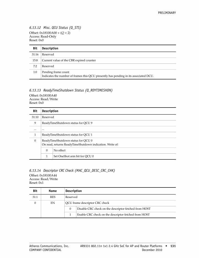
PRELIMINARY
6.13.12 Misc. QCU Status (Q_STS)Offset: 0x18100A00 + (Q < 2) Access: Read-Only Reset: 0x0
6.13.13 ReadyTimeShutdown Status (Q_RDYTIMESHDN)Offset: 0x18100A40 Access: Read/Write Reset: 0x0
6.13.14 Descriptor CRC Check (MAC_QCU_DESC_CRC_CHK)Offset: 0x18100A44 Access: Read/Write Reset: 0x1
Bit Description
31:16 Reserved
15:8 Current value of the CBR expired counter
7:2 Reserved
1:0 Pending frame countIndicates the number of frames this QCU presently has pending in its associated DCU.
Bit Description
31:10 Reserved
9 ReadyTimeShutdown status for QCU 9
... ...
1 ReadyTimeShutdown status for QCU 1
0 ReadyTimeShutdown status for QCU 0On read, returns ReadyTimeShutdown indication. Write of:
0 No effect
1 Set OneShot arm bit for QCU 0
Bit Name Description
31:1 RES Reserved
0 EN QCU frame descriptor CRC check
0 Disable CRC check on the descriptor fetched from HOST
1 Enable CRC check on the descriptor fetched from HOST
Atheros Communications, Inc. AR9331 802.11n 1x1 2.4 GHz SoC for AP and Router Platforms • 131 COMPANY CONFIDENTIAL December 2010 • 131

PRELIMINARY
6.14 DCU RegistersThe DCU registers occupy the offset range 0x18101000– 0x181012F0 in the AR9331 address space. The AR9331 has ten DCUs, numbered from 0 to 9.
6.14.1 QCU Mask (D_QCUMASK)Offset: 0x18101000 + (D < 2) Access: Read/Write Cold Reset: 0x0 Warm Reset: Unaffected
NOTE: To achieve lowest power consumption, software should set this register to 0x0 for all DCUs that are not in use. The hardware detects that the QCU mask is set to zero and shuts down certain logic in response, helping to save power.
Table 6-8. QCU Registers
Offset Name Description Page
0x18101000 + (D << 2)[1] D_QCUMASK QCU Mask page 132
0x18101040 + (D << 2)[1] D_LCL_IFS DCU-Specific IFS Settings page 133
0x18101080 + (D << 2)[1] D_RETRY_LIMIT Retry Limits page 133
0x181010C0 + (D << 2)[1] D_CHNTIME ChannelTime Settings page 134
0x18101100 + (D << 2)[1] D_MISC Miscellaneous DCU-Specific Settings page 134
0x18101030 D_GBL_IFS_SIFS DCU-Global IFS Settings: SIFS Duration page 135
0x18101070 D_GBL_IFS_SLOT DCU-Global IFS Settings: Slot Duration page 135
0x181010B0 D_GBL_IFS_EIFS DCU-Global IFS Settings: EIFS Duration page 135
0x181010F0 D_GBL_IFS_MISC DCU-Global IFS Settings: Misc. Parameters page 136
0x18101270 D_TXPSE DCU Transmit Pause Control/Status page 136
0x181012F0 D_TXSLOTMASK DCU Transmission Slot Mask page 137
[1]The variable D in the register addresses refers to the DCU number.
Bit Name Description
31:10 RES Reserved
9:0 QCU_MASK QCU maskSetting bit Q means that QCU Q is associated with (i.e., feeds into) this DCU. These register have reset values which corresponding to a 1 to 1 mapping between QCUs and DCUs. A register offset of 0x1000 maps to 0x1, 0x1004 maps to 0x2, 0x1008 maps to 0x4, etc.
132 • AR9331 802.11n 1x1 2.4 GHz SoC for AP and Router Platforms Atheros Communications, Inc. 132 • December 2010 COMPANY CONFIDENTIAL
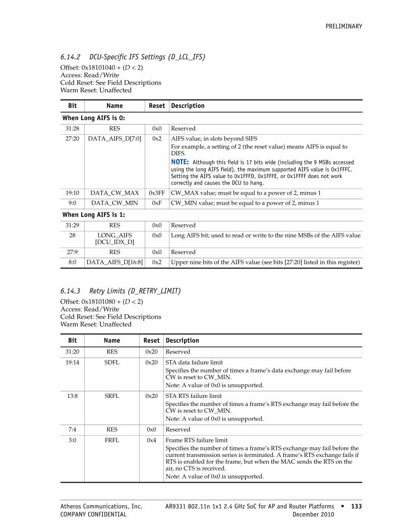
PRELIMINARY
6.14.2 DCU-Specific IFS Settings (D_LCL_IFS)Offset: 0x18101040 + (D < 2) Access: Read/Write Cold Reset: See Field Descriptions Warm Reset: Unaffected
6.14.3 Retry Limits (D_RETRY_LIMIT)Offset: 0x18101080 + (D < 2) Access: Read/Write Cold Reset: See Field Descriptions Warm Reset: Unaffected
Bit Name Reset Description
When Long AIFS is 0:31:28 RES 0x0 Reserved
27:20 DATA_AIFS_D[7:0] 0x2 AIFS value, in slots beyond SIFSFor example, a setting of 2 (the reset value) means AIFS is equal to DIFS. NOTE: Although this field is 17 bits wide (including the 9 MSBs accessed using the long AIFS field), the maximum supported AIFS value is 0x1FFFC. Setting the AIFS value to 0x1FFFD, 0x1FFFE, or 0x1FFFF does not work correctly and causes the DCU to hang.
19:10 DATA_CW_MAX 0x3FF CW_MAX value; must be equal to a power of 2, minus 1
9:0 DATA_CW_MIN 0xF CW_MIN value; must be equal to a power of 2, minus 1
When Long AIFS is 1:31:29 RES 0x0 Reserved
28 LONG_AIFS[DCU_IDX_D]
0x0 Long AIFS bit; used to read or write to the nine MSBs of the AIFS value
27:9 RES 0x0 Reserved
8:0 DATA_AIFS_D[16:8] 0x2 Upper nine bits of the AIFS value (see bits [27:20] listed in this register)
Bit Name Reset Description
31:20 RES 0x20 Reserved
19:14 SDFL 0x20 STA data failure limitSpecifies the number of times a frame’s data exchange may fail before CW is reset to CW_MIN. Note: A value of 0x0 is unsupported.
13:8 SRFL 0x20 STA RTS failure limitSpecifies the number of times a frame’s RTS exchange may fail before the CW is reset to CW_MIN. Note: A value of 0x0 is unsupported.
7:4 RES 0x0 Reserved
3:0 FRFL 0x4 Frame RTS failure limitSpecifies the number of times a frame’s RTS exchange may fail before the current transmission series is terminated. A frame’s RTS exchange fails if RTS is enabled for the frame, but when the MAC sends the RTS on the air, no CTS is received.Note: A value of 0x0 is unsupported.
Atheros Communications, Inc. AR9331 802.11n 1x1 2.4 GHz SoC for AP and Router Platforms • 133 COMPANY CONFIDENTIAL December 2010 • 133
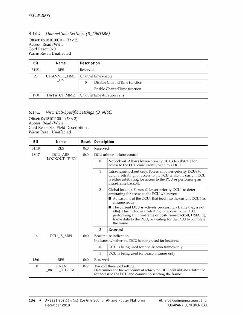
PRELIMINARY
6.14.4 ChannelTime Settings (D_CHNTIME)Offset: 0x181010C0 + (D < 2) Access: Read/Write Cold Reset: 0x0 Warm Reset: Unaffected
6.14.5 Misc. DCU-Specific Settings (D_MISC)Offset: 0x18101100 + (D < 2) Access: Read/Write Cold Reset: See Field Descriptions Warm Reset: Unaffected
Bit Name Description
31:21 RES Reserved
20 CHANNEL_TIME_EN
ChannelTime enable
0 Disable ChannelTime function
1 Enable ChannelTime function
19:0 DATA_CT_MMR ChannelTime duration in μs
Bit Name Reset Description
31:19 RES 0x0 Reserved
18:17 DCU_ARB_LOCKOUT_IF_EN
0x0 DCU arbiter lockout control
0 No lockout. Allows lower-priority DCUs to arbitrate for access to the PCU concurrently with this DCU.
1 Intra-frame lockout only. Forces all lower-priority DCUs to defer arbitrating for access to the PCU while the current DCU is either arbitrating for access to the PCU or performing an intra-frame backoff.
2 Global lockout. Forces all lower-priority DCUs to defer arbitrating for access to the PCU whenever: ■ At least one of the QCUs that feed into the current DCU has
a frame ready■ The current DCU is actively processing a frame (i.e., is not
idle). This includes arbitrating for access to the PCU, performing an intra-frame or post-frame backoff, DMA'ing frame data to the PCU, or waiting for the PCU to complete the frame.
3 Reserved
16 DCU_IS_BRN 0x0 Beacon use indicationIndicates whether the DCU is being used for beacons.
0 DCU is being used for non-beacon frames only
1 DCU is being used for beacon frames only
15:6 RES 0x0 Reserved
5:0 DATA_BKOFF_THRESH
0x2 Backoff threshold setting Determines the backoff count at which the DCU will initiate arbitration for access to the PCU and commit to sending the frame.
134 • AR9331 802.11n 1x1 2.4 GHz SoC for AP and Router Platforms Atheros Communications, Inc. 134 • December 2010 COMPANY CONFIDENTIAL
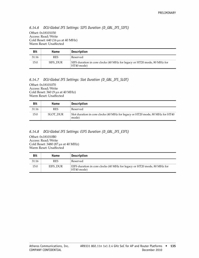
PRELIMINARY
6.14.6 DCU-Global IFS Settings: SIFS Duration (D_GBL_IFS_SIFS)Offset: 0x18101030 Access: Read/Write Cold Reset: 640 (16 μs at 40 MHz) Warm Reset: Unaffected
6.14.7 DCU-Global IFS Settings: Slot Duration (D_GBL_IFS_SLOT)Offset: 0x18101070 Access: Read/Write Cold Reset: 360 (9 μs at 40 MHz) Warm Reset: Unaffected
6.14.8 DCU-Global IFS Settings: EIFS Duration (D_GBL_IFS_EIFS)Offset: 0x181010B0 Access: Read/Write Cold Reset: 3480 (87 μs at 40 MHz) Warm Reset: Unaffected
Bit Name Description
31:16 RES Reserved
15:0 SIFS_DUR SIFS duration in core clocks (40 MHz for legacy or HT20 mode, 80 MHz for HT40 mode)
Bit Name Description
31:16 RES Reserved
15:0 SLOT_DUR Slot duration in core clocks (40 MHz for legacy or HT20 mode, 80 MHz for HT40 mode)
Bit Name Description
31:16 RES Reserved
15:0 EIFS_DUR EIFS duration in core clocks (40 MHz for legacy or HT20 mode, 80 MHz for HT40 mode)
Atheros Communications, Inc. AR9331 802.11n 1x1 2.4 GHz SoC for AP and Router Platforms • 135 COMPANY CONFIDENTIAL December 2010 • 135
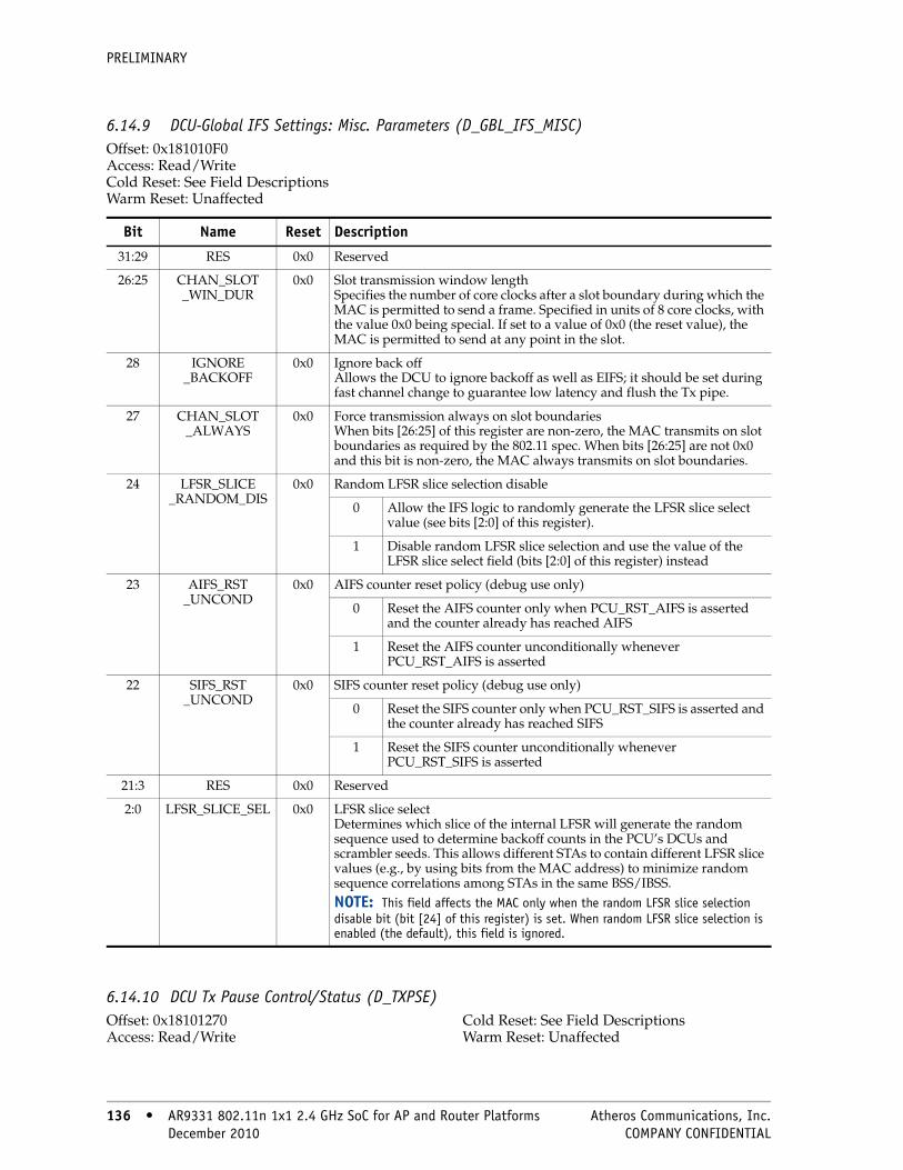
PRELIMINARY
6.14.9 DCU-Global IFS Settings: Misc. Parameters (D_GBL_IFS_MISC)Offset: 0x181010F0 Access: Read/Write Cold Reset: See Field Descriptions Warm Reset: Unaffected
6.14.10 DCU Tx Pause Control/Status (D_TXPSE)Offset: 0x18101270 Access: Read/Write
Cold Reset: See Field Descriptions Warm Reset: Unaffected
Bit Name Reset Description
31:29 RES 0x0 Reserved
26:25 CHAN_SLOT_WIN_DUR
0x0 Slot transmission window length Specifies the number of core clocks after a slot boundary during which the MAC is permitted to send a frame. Specified in units of 8 core clocks, with the value 0x0 being special. If set to a value of 0x0 (the reset value), the MAC is permitted to send at any point in the slot.
28 IGNORE_BACKOFF
0x0 Ignore back off Allows the DCU to ignore backoff as well as EIFS; it should be set during fast channel change to guarantee low latency and flush the Tx pipe.
27 CHAN_SLOT_ALWAYS
0x0 Force transmission always on slot boundaries When bits [26:25] of this register are non-zero, the MAC transmits on slot boundaries as required by the 802.11 spec. When bits [26:25] are not 0x0 and this bit is non-zero, the MAC always transmits on slot boundaries.
24 LFSR_SLICE_RANDOM_DIS
0x0 Random LFSR slice selection disable
0 Allow the IFS logic to randomly generate the LFSR slice select value (see bits [2:0] of this register).
1 Disable random LFSR slice selection and use the value of the LFSR slice select field (bits [2:0] of this register) instead
23 AIFS_RST_UNCOND
0x0 AIFS counter reset policy (debug use only)
0 Reset the AIFS counter only when PCU_RST_AIFS is asserted and the counter already has reached AIFS
1 Reset the AIFS counter unconditionally whenever PCU_RST_AIFS is asserted
22 SIFS_RST_UNCOND
0x0 SIFS counter reset policy (debug use only)
0 Reset the SIFS counter only when PCU_RST_SIFS is asserted and the counter already has reached SIFS
1 Reset the SIFS counter unconditionally whenever PCU_RST_SIFS is asserted
21:3 RES 0x0 Reserved
2:0 LFSR_SLICE_SEL 0x0 LFSR slice select Determines which slice of the internal LFSR will generate the random sequence used to determine backoff counts in the PCU’s DCUs and scrambler seeds. This allows different STAs to contain different LFSR slice values (e.g., by using bits from the MAC address) to minimize random sequence correlations among STAs in the same BSS/IBSS.NOTE: This field affects the MAC only when the random LFSR slice selection disable bit (bit [24] of this register) is set. When random LFSR slice selection is enabled (the default), this field is ignored.
136 • AR9331 802.11n 1x1 2.4 GHz SoC for AP and Router Platforms Atheros Communications, Inc. 136 • December 2010 COMPANY CONFIDENTIAL
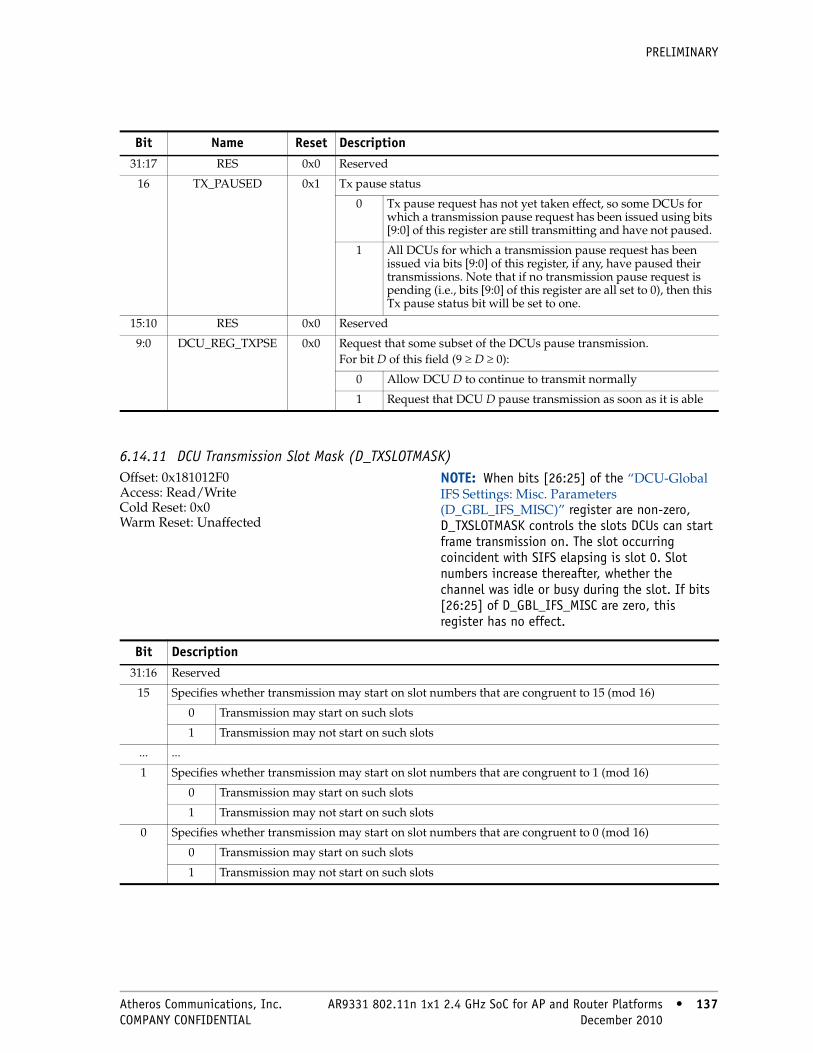
PRELIMINARY
6.14.11 DCU Transmission Slot Mask (D_TXSLOTMASK)Offset: 0x181012F0 Access: Read/Write Cold Reset: 0x0 Warm Reset: Unaffected
NOTE: When bits [26:25] of the “DCU-Global IFS Settings: Misc. Parameters (D_GBL_IFS_MISC)” register are non-zero, D_TXSLOTMASK controls the slots DCUs can start frame transmission on. The slot occurring coincident with SIFS elapsing is slot 0. Slot numbers increase thereafter, whether the channel was idle or busy during the slot. If bits [26:25] of D_GBL_IFS_MISC are zero, this register has no effect.
Bit Name Reset Description31:17 RES 0x0 Reserved
16 TX_PAUSED 0x1 Tx pause status
0 Tx pause request has not yet taken effect, so some DCUs for which a transmission pause request has been issued using bits [9:0] of this register are still transmitting and have not paused.
1 All DCUs for which a transmission pause request has been issued via bits [9:0] of this register, if any, have paused their transmissions. Note that if no transmission pause request is pending (i.e., bits [9:0] of this register are all set to 0), then this Tx pause status bit will be set to one.
15:10 RES 0x0 Reserved
9:0 DCU_REG_TXPSE 0x0 Request that some subset of the DCUs pause transmission. For bit D of this field (9 ≥ D ≥ 0):
0 Allow DCU D to continue to transmit normally
1 Request that DCU D pause transmission as soon as it is able
Bit Description31:16 Reserved
15 Specifies whether transmission may start on slot numbers that are congruent to 15 (mod 16)
0 Transmission may start on such slots
1 Transmission may not start on such slots
... ...
1 Specifies whether transmission may start on slot numbers that are congruent to 1 (mod 16)
0 Transmission may start on such slots
1 Transmission may not start on such slots
0 Specifies whether transmission may start on slot numbers that are congruent to 0 (mod 16)
0 Transmission may start on such slots
1 Transmission may not start on such slots
Atheros Communications, Inc. AR9331 802.11n 1x1 2.4 GHz SoC for AP and Router Platforms • 137 COMPANY CONFIDENTIAL December 2010 • 137
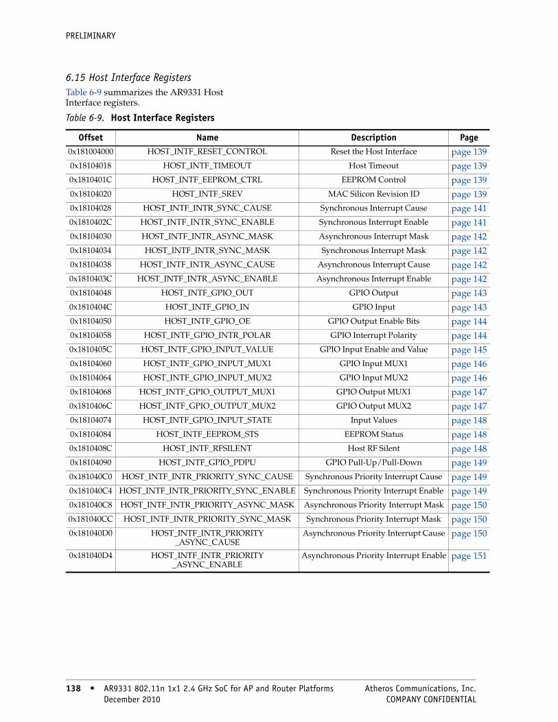
PRELIMINARY
6.15 Host Interface RegistersTable 6-9 summarizes the AR9331 Host Interface registers.
Table 6-9. Host Interface Registers
Offset Name Description Page0x181004000 HOST_INTF_RESET_CONTROL Reset the Host Interface page 1390x18104018 HOST_INTF_TIMEOUT Host Timeout page 1390x1810401C HOST_INTF_EEPROM_CTRL EEPROM Control page 1390x18104020 HOST_INTF_SREV MAC Silicon Revision ID page 1390x18104028 HOST_INTF_INTR_SYNC_CAUSE Synchronous Interrupt Cause page 1410x1810402C HOST_INTF_INTR_SYNC_ENABLE Synchronous Interrupt Enable page 1410x18104030 HOST_INTF_INTR_ASYNC_MASK Asynchronous Interrupt Mask page 1420x18104034 HOST_INTF_INTR_SYNC_MASK Synchronous Interrupt Mask page 1420x18104038 HOST_INTF_INTR_ASYNC_CAUSE Asynchronous Interrupt Cause page 1420x1810403C HOST_INTF_INTR_ASYNC_ENABLE Asynchronous Interrupt Enable page 1420x18104048 HOST_INTF_GPIO_OUT GPIO Output page 1430x1810404C HOST_INTF_GPIO_IN GPIO Input page 1430x18104050 HOST_INTF_GPIO_OE GPIO Output Enable Bits page 1440x18104058 HOST_INTF_GPIO_INTR_POLAR GPIO Interrupt Polarity page 1440x1810405C HOST_INTF_GPIO_INPUT_VALUE GPIO Input Enable and Value page 1450x18104060 HOST_INTF_GPIO_INPUT_MUX1 GPIO Input MUX1 page 1460x18104064 HOST_INTF_GPIO_INPUT_MUX2 GPIO Input MUX2 page 1460x18104068 HOST_INTF_GPIO_OUTPUT_MUX1 GPIO Output MUX1 page 1470x1810406C HOST_INTF_GPIO_OUTPUT_MUX2 GPIO Output MUX2 page 1470x18104074 HOST_INTF_GPIO_INPUT_STATE Input Values page 1480x18104084 HOST_INTF_EEPROM_STS EEPROM Status page 1480x1810408C HOST_INTF_RFSILENT Host RF Silent page 1480x18104090 HOST_INTF_GPIO_PDPU GPIO Pull-Up/Pull-Down page 1490x181040C0 HOST_INTF_INTR_PRIORITY_SYNC_CAUSE Synchronous Priority Interrupt Cause page 1490x181040C4 HOST_INTF_INTR_PRIORITY_SYNC_ENABLE Synchronous Priority Interrupt Enable page 1490x181040C8 HOST_INTF_INTR_PRIORITY_ASYNC_MASK Asynchronous Priority Interrupt Mask page 1500x181040CC HOST_INTF_INTR_PRIORITY_SYNC_MASK Synchronous Priority Interrupt Mask page 1500x181040D0 HOST_INTF_INTR_PRIORITY
_ASYNC_CAUSEAsynchronous Priority Interrupt Cause page 150
0x181040D4 HOST_INTF_INTR_PRIORITY_ASYNC_ENABLE
Asynchronous Priority Interrupt Enable page 151
138 • AR9331 802.11n 1x1 2.4 GHz SoC for AP and Router Platforms Atheros Communications, Inc. 138 • December 2010 COMPANY CONFIDENTIAL
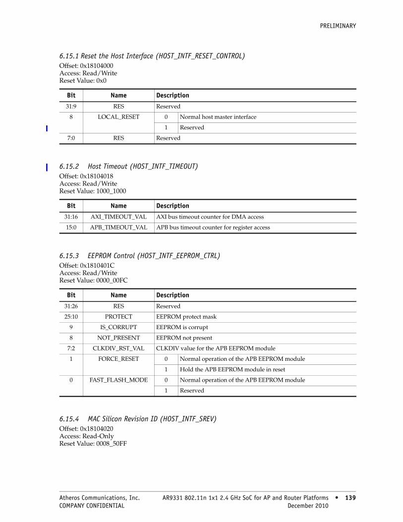
PRELIMINARY
6.15.1 Reset the Host Interface (HOST_INTF_RESET_CONTROL)Offset: 0x18104000 Access: Read/Write Reset Value: 0x0
6.15.2 Host Timeout (HOST_INTF_TIMEOUT)Offset: 0x18104018 Access: Read/Write Reset Value: 1000_1000
6.15.3 EEPROM Control (HOST_INTF_EEPROM_CTRL)Offset: 0x1810401C Access: Read/Write Reset Value: 0000_00FC
6.15.4 MAC Silicon Revision ID (HOST_INTF_SREV)Offset: 0x18104020 Access: Read-Only Reset Value: 0008_50FF
Bit Name Description
31:9 RES Reserved
8 LOCAL_RESET 0 Normal host master interface
1 Reserved
7:0 RES Reserved
Bit Name Description
31:16 AXI_TIMEOUT_VAL AXI bus timeout counter for DMA access
15:0 APB_TIMEOUT_VAL APB bus timeout counter for register access
Bit Name Description
31:26 RES Reserved
25:10 PROTECT EEPROM protect mask
9 IS_CORRUPT EEPROM is corrupt
8 NOT_PRESENT EEPROM not present
7:2 CLKDIV_RST_VAL CLKDIV value for the APB EEPROM module
1 FORCE_RESET 0 Normal operation of the APB EEPROM module
1 Hold the APB EEPROM module in reset
0 FAST_FLASH_MODE 0 Normal operation of the APB EEPROM module
1 Reserved
Atheros Communications, Inc. AR9331 802.11n 1x1 2.4 GHz SoC for AP and Router Platforms • 139 COMPANY CONFIDENTIAL December 2010 • 139
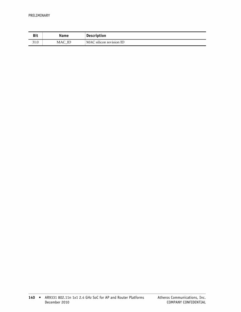
PRELIMINARY
Bit Name Description
31:0 MAC_ID MAC silicon revision ID
140 • AR9331 802.11n 1x1 2.4 GHz SoC for AP and Router Platforms Atheros Communications, Inc. 140 • December 2010 COMPANY CONFIDENTIAL
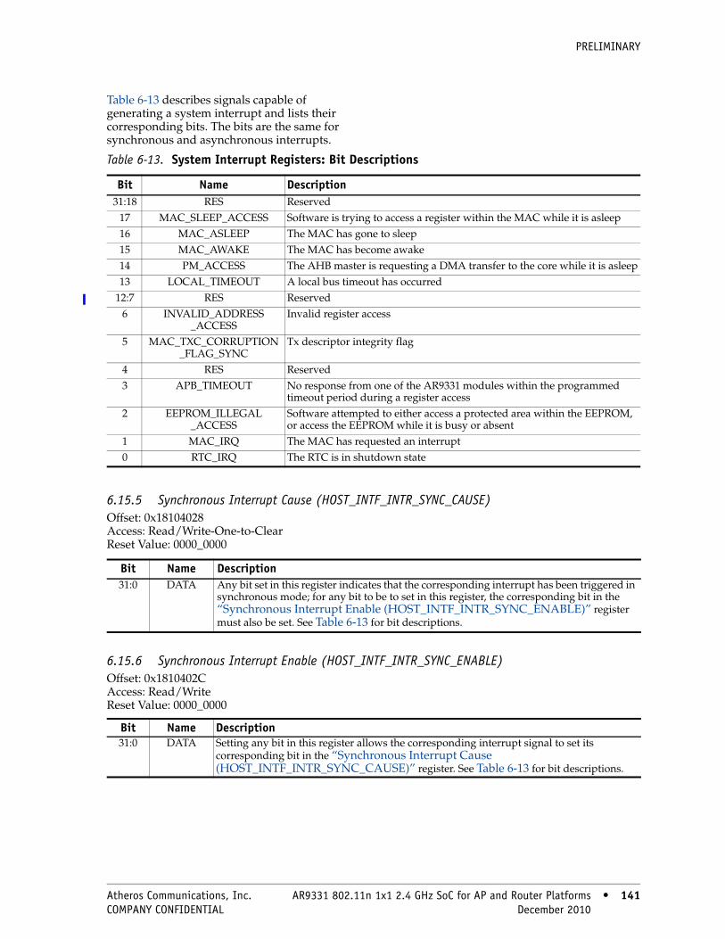
PRELIMINARY
Table 6-13 describes signals capable of generating a system interrupt and lists their corresponding bits. The bits are the same for synchronous and asynchronous interrupts.
6.15.5 Synchronous Interrupt Cause (HOST_INTF_INTR_SYNC_CAUSE)Offset: 0x18104028 Access: Read/Write-One-to-Clear Reset Value: 0000_0000
6.15.6 Synchronous Interrupt Enable (HOST_INTF_INTR_SYNC_ENABLE)Offset: 0x1810402C Access: Read/Write Reset Value: 0000_0000
Table 6-13. System Interrupt Registers: Bit Descriptions
Bit Name Description31:18 RES Reserved
17 MAC_SLEEP_ACCESS Software is trying to access a register within the MAC while it is asleep16 MAC_ASLEEP The MAC has gone to sleep15 MAC_AWAKE The MAC has become awake14 PM_ACCESS The AHB master is requesting a DMA transfer to the core while it is asleep13 LOCAL_TIMEOUT A local bus timeout has occurred
12:7 RES Reserved6 INVALID_ADDRESS
_ACCESSInvalid register access
5 MAC_TXC_CORRUPTION_FLAG_SYNC
Tx descriptor integrity flag
4 RES Reserved3 APB_TIMEOUT No response from one of the AR9331 modules within the programmed
timeout period during a register access2 EEPROM_ILLEGAL
_ACCESSSoftware attempted to either access a protected area within the EEPROM, or access the EEPROM while it is busy or absent
1 MAC_IRQ The MAC has requested an interrupt0 RTC_IRQ The RTC is in shutdown state
Bit Name Description31:0 DATA Any bit set in this register indicates that the corresponding interrupt has been triggered in
synchronous mode; for any bit to be to set in this register, the corresponding bit in the “Synchronous Interrupt Enable (HOST_INTF_INTR_SYNC_ENABLE)” register must also be set. See Table 6-13 for bit descriptions.
Bit Name Description31:0 DATA Setting any bit in this register allows the corresponding interrupt signal to set its
corresponding bit in the “Synchronous Interrupt Cause (HOST_INTF_INTR_SYNC_CAUSE)” register. See Table 6-13 for bit descriptions.
Atheros Communications, Inc. AR9331 802.11n 1x1 2.4 GHz SoC for AP and Router Platforms • 141 COMPANY CONFIDENTIAL December 2010 • 141
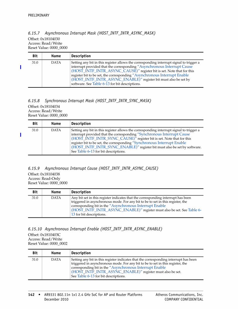
PRELIMINARY
6.15.7 Asynchronous Interrupt Mask (HOST_INTF_INTR_ASYNC_MASK)Offset: 0x18104030 Access: Read/Write Reset Value: 0000_0000
6.15.8 Synchronous Interrupt Mask (HOST_INTF_INTR_SYNC_MASK)Offset: 0x18104034 Access: Read/Write Reset Value: 0000_0000
6.15.9 Asynchronous Interrupt Cause (HOST_INTF_INTR_ASYNC_CAUSE)Offset: 0x18104038 Access: Read-Only Reset Value: 0000_0000
6.15.10 Asynchronous Interrupt Enable (HOST_INTF_INTR_ASYNC_ENABLE)Offset: 0x1810403C Access: Read/Write Reset Value: 0000_0002
Bit Name Description
31:0 DATA Setting any bit in this register allows the corresponding interrupt signal to trigger a interrupt provided that the corresponding “Asynchronous Interrupt Cause (HOST_INTF_INTR_ASYNC_CAUSE)” register bit is set. Note that for this register bit to be set, the corresponding “Asynchronous Interrupt Enable (HOST_INTF_INTR_ASYNC_ENABLE)” register bit must also be set by software. See Table 6-13 for bit descriptions.
Bit Name Description
31:0 DATA Setting any bit in this register allows the corresponding interrupt signal to trigger a interrupt provided that the corresponding “Synchronous Interrupt Cause (HOST_INTF_INTR_SYNC_CAUSE)” register bit is set. Note that for this register bit to be set, the corresponding “Synchronous Interrupt Enable (HOST_INTF_INTR_SYNC_ENABLE)” register bit must also be set by software. See Table 6-13 for bit descriptions.
Bit Name Description31:0 DATA Any bit set in this register indicates that the corresponding interrupt has been
triggered in asynchronous mode. For any bit to be to set in this register, the corresponding bit in the “Asynchronous Interrupt Enable (HOST_INTF_INTR_ASYNC_ENABLE)” register must also be set. See Table 6-13 for bit descriptions.
Bit Name Description
31:0 DATA Setting any bit in this register indicates that the corresponding interrupt has been triggered in asynchronous mode. For any bit to be to set in this register, the corresponding bit in the “Asynchronous Interrupt Enable (HOST_INTF_INTR_ASYNC_ENABLE)” register must also be set. See Table 6-13 for bit descriptions.
142 • AR9331 802.11n 1x1 2.4 GHz SoC for AP and Router Platforms Atheros Communications, Inc. 142 • December 2010 COMPANY CONFIDENTIAL
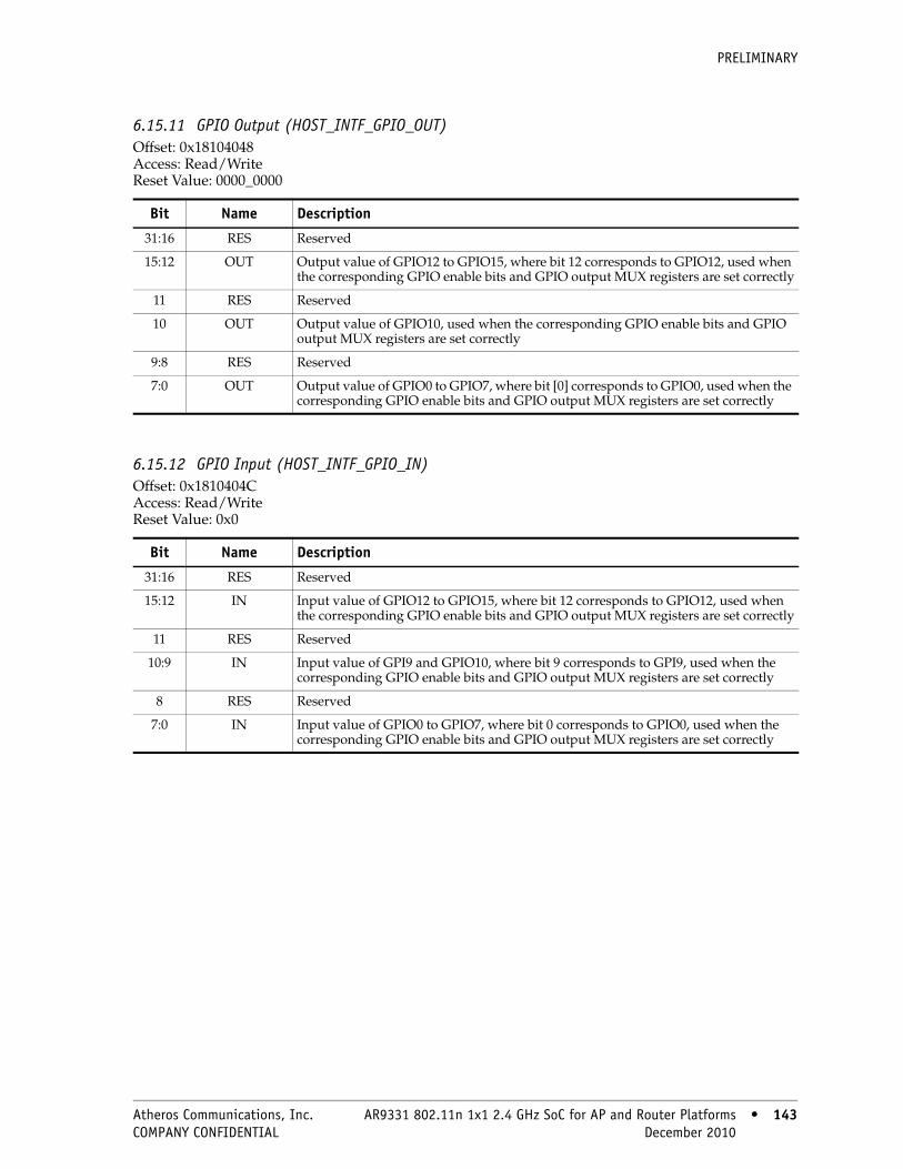
PRELIMINARY
6.15.11 GPIO Output (HOST_INTF_GPIO_OUT)Offset: 0x18104048 Access: Read/Write Reset Value: 0000_0000
6.15.12 GPIO Input (HOST_INTF_GPIO_IN)Offset: 0x1810404C Access: Read/Write Reset Value: 0x0
Bit Name Description
31:16 RES Reserved
15:12 OUT Output value of GPIO12 to GPIO15, where bit 12 corresponds to GPIO12, used when the corresponding GPIO enable bits and GPIO output MUX registers are set correctly
11 RES Reserved
10 OUT Output value of GPIO10, used when the corresponding GPIO enable bits and GPIO output MUX registers are set correctly
9:8 RES Reserved
7:0 OUT Output value of GPIO0 to GPIO7, where bit [0] corresponds to GPIO0, used when the corresponding GPIO enable bits and GPIO output MUX registers are set correctly
Bit Name Description
31:16 RES Reserved
15:12 IN Input value of GPIO12 to GPIO15, where bit 12 corresponds to GPIO12, used when the corresponding GPIO enable bits and GPIO output MUX registers are set correctly
11 RES Reserved
10:9 IN Input value of GPI9 and GPIO10, where bit 9 corresponds to GPI9, used when the corresponding GPIO enable bits and GPIO output MUX registers are set correctly
8 RES Reserved
7:0 IN Input value of GPIO0 to GPIO7, where bit 0 corresponds to GPIO0, used when the corresponding GPIO enable bits and GPIO output MUX registers are set correctly
Atheros Communications, Inc. AR9331 802.11n 1x1 2.4 GHz SoC for AP and Router Platforms • 143 COMPANY CONFIDENTIAL December 2010 • 143

PRELIMINARY
6.15.13 Host GPIO Output Enable Bits (HOST_INTF_GPIO_OE)Offset: 0x18104050 Access: Read/Write Reset Value: 0x0
NOTE: Each 2-bit field controls the drive mechanism for each GPIO (bits [1:0] correspond to GPIO0, bits [3:2] correspond to GPIO1, etc.) The mapping for this 2-bit field is:
■ 0 = Never drive output■ 1 = Drive if output is low■ 2 = Drive if output is high■ 3 = Always drive output
6.15.14 Host GPIO Interrupt Polarity (HOST_INTF_GPIO_INTR_POLAR)Offset: 0x18104058 Access: Read/Write Reset Value: 0x0
Bit NAME Description
31:24 DATA Host GPIO output enable bits for GPIO12 to GPIO15
23:22 RES Reserved
21:20 DATA Host GPIO output enable bits for GPIO10
19:16 RES Reserved
15:0 DATA Host GPIO output enable bits for GPIO0 to GPIO7, every two bits corresponds to each GPIO, bits[1:0] for GPIO0, bits[3:2] for GPIO1, etc.
Bit NAME Description
31:16 RES Reserved
15:12 DATA Host GPIO interrupt polarity for GPIO12 to GPIO15, bit 12 corresponds to GPIO12
0 Active low
1 Active high
11 RES Reserved
10:9 DATA Host GPIO interrupt polarity for GPI9 and GPIO10, bit 9 corresponds to GPI9
0 Active low
1 Active high
8 RES Reserved
DATA DATA Host GPIO interrupt polarity for GPIO0 to GPIO7, bit 0 corresponds to GPIO0
0 Active low
1 Active high
144 • AR9331 802.11n 1x1 2.4 GHz SoC for AP and Router Platforms Atheros Communications, Inc. 144 • December 2010 COMPANY CONFIDENTIAL
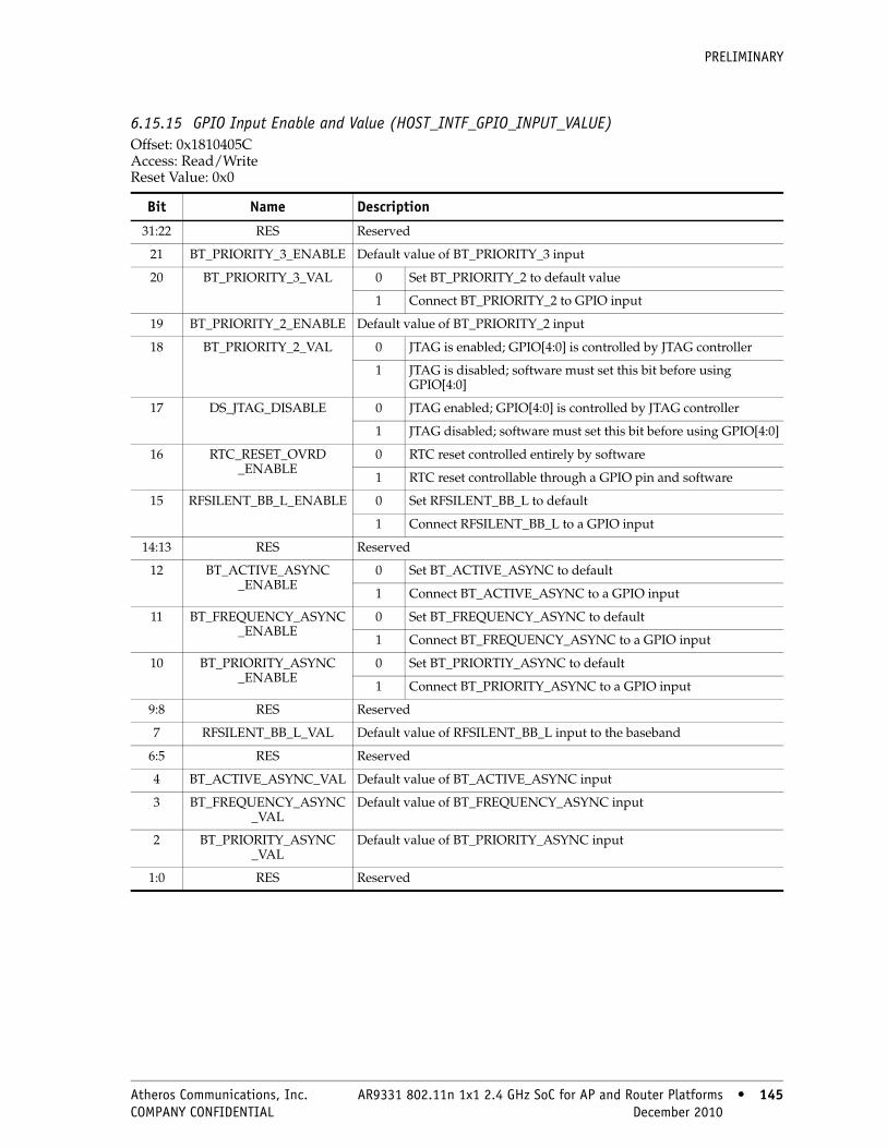
PRELIMINARY
6.15.15 GPIO Input Enable and Value (HOST_INTF_GPIO_INPUT_VALUE)Offset: 0x1810405C Access: Read/Write Reset Value: 0x0
Bit Name Description
31:22 RES Reserved
21 BT_PRIORITY_3_ENABLE Default value of BT_PRIORITY_3 input
20 BT_PRIORITY_3_VAL 0 Set BT_PRIORITY_2 to default value
1 Connect BT_PRIORITY_2 to GPIO input
19 BT_PRIORITY_2_ENABLE Default value of BT_PRIORITY_2 input
18 BT_PRIORITY_2_VAL 0 JTAG is enabled; GPIO[4:0] is controlled by JTAG controller
1 JTAG is disabled; software must set this bit before using GPIO[4:0]
17 DS_JTAG_DISABLE 0 JTAG enabled; GPIO[4:0] is controlled by JTAG controller
1 JTAG disabled; software must set this bit before using GPIO[4:0]
16 RTC_RESET_OVRD_ENABLE
0 RTC reset controlled entirely by software
1 RTC reset controllable through a GPIO pin and software
15 RFSILENT_BB_L_ENABLE 0 Set RFSILENT_BB_L to default
1 Connect RFSILENT_BB_L to a GPIO input
14:13 RES Reserved
12 BT_ACTIVE_ASYNC_ENABLE
0 Set BT_ACTIVE_ASYNC to default
1 Connect BT_ACTIVE_ASYNC to a GPIO input
11 BT_FREQUENCY_ASYNC_ENABLE
0 Set BT_FREQUENCY_ASYNC to default
1 Connect BT_FREQUENCY_ASYNC to a GPIO input
10 BT_PRIORITY_ASYNC_ENABLE
0 Set BT_PRIORTIY_ASYNC to default
1 Connect BT_PRIORITY_ASYNC to a GPIO input
9:8 RES Reserved
7 RFSILENT_BB_L_VAL Default value of RFSILENT_BB_L input to the baseband
6:5 RES Reserved
4 BT_ACTIVE_ASYNC_VAL Default value of BT_ACTIVE_ASYNC input
3 BT_FREQUENCY_ASYNC_VAL
Default value of BT_FREQUENCY_ASYNC input
2 BT_PRIORITY_ASYNC_VAL
Default value of BT_PRIORITY_ASYNC input
1:0 RES Reserved
Atheros Communications, Inc. AR9331 802.11n 1x1 2.4 GHz SoC for AP and Router Platforms • 145 COMPANY CONFIDENTIAL December 2010 • 145

PRELIMINARY
6.15.16 GPIO Input MUX1 (HOST_INTF_GPIO_INPUT_MUX1)Offset: 0x18104060 Access: Read/Write Reset Value: 0x0
NOTE: Functionality described in each 4-bit register field can be mapped to GPIO10, GPI9, and GPIO [7:0].
For example, to select GPI9 to be used as BT_ACTIVE input, write 0x9 to bits [19:16], the SEL_4 bit field.
6.15.17 GPIO Input MUX2 (HOST_INTF_GPIO_INPUT_MUX2)Offset: 0x18104064 Access: Read/Write Reset Value: 0x0
NOTE: Functionality described in each 4-bit register field can be mapped to GPIO10, GPI9, and GPIO [7:0].
For example, to select GPIO0 to be used as BT_PRIORITY_2 input, write 0x0 to bits [15:12], the SEL_9 bit field.
Bit Name Description
31:20 RES Reserved
19:16 SEL_4 GPIO[sel_4] will connect to BT_ACTIVE input, if BT_ACTIVE_ENABLE is set
15:12 SEL_3 GPIO[sel_3] will connect to BT_FREQUENCY input, if BT_FREQUENCY_ENABLE is set
11:8 SEL_2 GPIO[sel_2] will connect to BT_PRIORITY input, if BT_PRIORITY_ENABLE is set
7:4 RES Reserved
3:0 RST_TSF GPIO[sel_0] will connect to RST_TSF input, if GPIO_RST_TSF_ENABLE is set. For example, if 5 is set to this SEL_0, GPIO[5] will be connected to RST_TSF input if GPIO_RST_TSF_ENABLE is set
Bit Name Description
31:20 RES Reserved
19:16 SEL_10 GPIO[sel_10] will connect to BT_PRIORITY_3 input, if BT_PRIORITY_3_ENABLE is set.
15:12 SEL_9 GPIO[sel_9] will connect to BT_PRIORITY_2 input, if BT_PRIORITY_2_ENABLE is set
11:8 RES Reserved
7:4 SEL_7 GPIO[sel_7] will connect to RFSILENT_BB_L input, if RFSILENT_BB_L_ENABLE is set
3:0 RES Reserved
146 • AR9331 802.11n 1x1 2.4 GHz SoC for AP and Router Platforms Atheros Communications, Inc. 146 • December 2010 COMPANY CONFIDENTIAL

PRELIMINARY
Table 6-14 describes the output MUX setting for each GPIO. This table applies to HOST_INTF_GPIO_OUTPUT_MUX1, HOST_INTF_GPIO_OUTPUT_MUX2, and HOST_INTF_GPIO_OUTPUT_MUX3.
NOTE: Each of the GPIO pins controlled by these registers has 5 bits associated with it. Each GPIO can be configured to drive 1 of 32 output functions. See Table 6-14.
6.15.18 GPIO Output MUX1 (HOST_INTF_GPIO_OUTPUT_MUX1)Offset: 0x18104068 Access: Read/Write Reset Value: 0x0
NOTE: See Table 6-14. For example, to select GPIO2 to be used as WL_ACTIVE output, write 0x4 to bits [14:10], the SEL_2 bit field.
6.15.19 GPIO Output MUX2 (HOST_INTF_GPIO_OUTPUT_MUX2)Offset: 0x1810406C Access: Read/Write Reset Value: 0x0
NOTE: See Table 6-14. For example, to select GPIO7 to be used as External LNA control output, write 0x1F to bits [9:5], the SEL_7 bit field.
6.15.20 GPIO Output MUX3 (HOST_INTF_GPIO_OUTPUT_MUX3)Offset: 0x18104070 Access: Read/Write Reset Value: 0x0
See Table 6-14. For example, to select GPIO13 to be used as MAC network LED output, write 0x5 to bits [9:5], the SEL_13 bit field.
Table 6-14. Output MUX Values for Each GPIO; Set GPIO to:
Bit Description Bit Description Bit Description31 External LNA control 25:8 Reserved 3 MAC TX_FRAME
30:29 Reserved 7 Reserved 2 Reserved28 RX_CLEAR_EXTENSION 6 MAC power LED 1 Reserved27 BT_ANT 5 MAC network LED 0 The value set in the GPIO
output register26 MAC_WOW signal 4 WL_ACTIVE
Bit Name Description31:30 RES Reserved29:25 SEL_5 GPIO_OUTPUT_MUX[5] for GPIO524:20 SEL_4 GPIO_OUTPUT_MUX[4] for GPIO419:15 SEL_3 GPIO_OUTPUT_MUX[3] for GPIO314:10 SEL_2 GPIO_OUTPUT_MUX[2] for GPIO29:5 SEL_1 GPIO_OUTPUT_MUX[1] for GPIO14:0 SEL_0 GPIO_OUTPUT_MUX[0] for GPIO0
Bit Name Description31:26 RES Reserved24:20 SEL_10 GPIO_OUTPUT_MUX[10] for GPIO1019:10 RES Reserved9:5 SEL_7 GPIO_OUTPUT_MUX[7] for GPIO74:0 SEL_6 GPIO_OUTPUT_MUX[6] for GPIO6
Bit Name Description31:20 RES Reserved19:15 SEL_15 GPIO_OUTPUT_MUX[15] for GPIO1514:10 SEL_14 GPIO_OUTPUT_MUX[14] for GPIO14
9:5 SEL_13 GPIO_OUTPUT_MUX[13] for GPIO134:0 SEL_12 GPIO_OUTPUT_MUX[12] for GPIO12
Atheros Communications, Inc. AR9331 802.11n 1x1 2.4 GHz SoC for AP and Router Platforms • 147 COMPANY CONFIDENTIAL December 2010 • 147
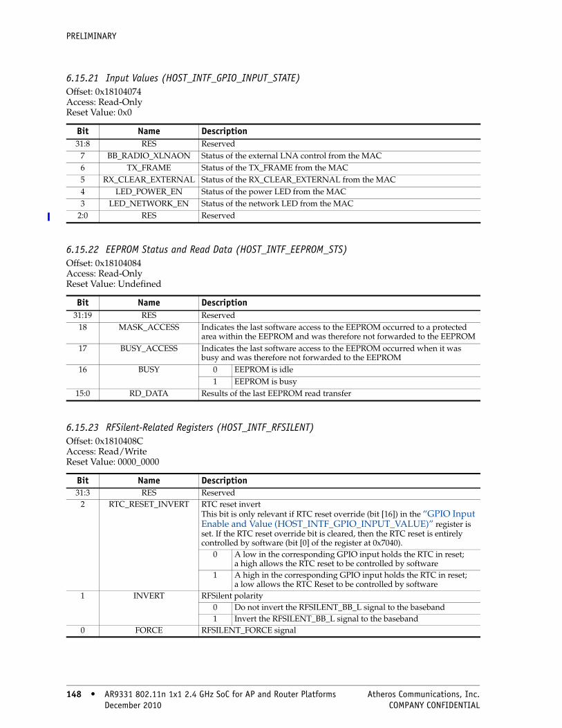
PRELIMINARY
6.15.21 Input Values (HOST_INTF_GPIO_INPUT_STATE)Offset: 0x18104074 Access: Read-Only Reset Value: 0x0
6.15.22 EEPROM Status and Read Data (HOST_INTF_EEPROM_STS)Offset: 0x18104084 Access: Read-Only Reset Value: Undefined
6.15.23 RFSilent-Related Registers (HOST_INTF_RFSILENT)Offset: 0x1810408C Access: Read/Write Reset Value: 0000_0000
Bit Name Description31:8 RES Reserved
7 BB_RADIO_XLNAON Status of the external LNA control from the MAC6 TX_FRAME Status of the TX_FRAME from the MAC5 RX_CLEAR_EXTERNAL Status of the RX_CLEAR_EXTERNAL from the MAC4 LED_POWER_EN Status of the power LED from the MAC3 LED_NETWORK_EN Status of the network LED from the MAC
2:0 RES Reserved
Bit Name Description31:19 RES Reserved
18 MASK_ACCESS Indicates the last software access to the EEPROM occurred to a protected area within the EEPROM and was therefore not forwarded to the EEPROM
17 BUSY_ACCESS Indicates the last software access to the EEPROM occurred when it was busy and was therefore not forwarded to the EEPROM
16 BUSY 0 EEPROM is idle1 EEPROM is busy
15:0 RD_DATA Results of the last EEPROM read transfer
Bit Name Description31:3 RES Reserved
2 RTC_RESET_INVERT RTC reset invert This bit is only relevant if RTC reset override (bit [16]) in the “GPIO Input Enable and Value (HOST_INTF_GPIO_INPUT_VALUE)” register is set. If the RTC reset override bit is cleared, then the RTC reset is entirely controlled by software (bit [0] of the register at 0x7040).
0 A low in the corresponding GPIO input holds the RTC in reset; a high allows the RTC reset to be controlled by software
1 A high in the corresponding GPIO input holds the RTC in reset; a low allows the RTC Reset to be controlled by software
1 INVERT RFSilent polarity0 Do not invert the RFSILENT_BB_L signal to the baseband1 Invert the RFSILENT_BB_L signal to the baseband
0 FORCE RFSILENT_FORCE signal
148 • AR9331 802.11n 1x1 2.4 GHz SoC for AP and Router Platforms Atheros Communications, Inc. 148 • December 2010 COMPANY CONFIDENTIAL

PRELIMINARY
6.15.24 GPIO Pull-Up/Pull-Down (HOST_INTF_GPIO_PDPU)Offset: 0x18104090 Access: Read/Write Reset Value: 0000_0001
NOTE: Each 2-bit field controls the drive mechanism for each GPIO (bits [1:0] correspond to GPIO0, bits [3:2] correspond to GPIO1, etc.) The mapping for this 2-bit field is:■ 0 = No pull-up or pull-down■ 1 = Pull-down■ 2 = Pull-up■ 3 = Reserved
6.15.25 Synchronous Priority Interrupt Cause (HOST_INTF_INTR_PRIORITY_SYNC_CAUSE)Offset: 0x181040C0 Access: Read/Write Reset Value: Undefined
6.15.26 Synchronous Priority Interrupt Enable (HOST_INTF_INTR_PRIORITY_SYNC_ENABLE)Offset: 0x181040C4 Access: Read/Write Reset Value: 0x0
Bit Name Description31:24 INT GPIO12 to GPIO15 pull-up or pull-down, bits [25:24] correspond to GPIO12
23:22 RES Reserved
21:18 INT GPI9 and GPIO10 pull-up or pull-down, bits [19:18] correspond to GPI9
17:16 RES Reserved
15:0 INT GPIO0 to GPIO 7 pull-up or pull-down
Bit Name Description31:3 RES Reserved
2:0 DATA Writing a 1 to any bit in this register clears the corresponding bit.
■ Any bit set to 1 in this register indicates the interrupt has been triggered in synchronous mode
■ Any bit set to 0 in this register indicates the corresponding bit in the “Synchronous Priority Interrupt Enable (HOST_INTF_INTR_PRIORITY_SYNC_ENABLE)” register must also be set by software
Bit[0] Tx interrupt triggered
Bit[1] Rx Low priority interrupt triggered
Bit[2] Rx High priority interrupt triggered
Bit Name Description31:3 RES Reserved
2:0 DATA Writing a 1 to a bit in this register allows the interrupt signal to set its corresponding bit in the “Synchronous Priority Interrupt Cause (HOST_INTF_INTR_PRIORITY_SYNC_CAUSE)” register.
Bit[0] Tx interrupt enable
Bit[1] Rx low priority interrupt enable
Bit[2] Rx high priority interrupt enable
Atheros Communications, Inc. AR9331 802.11n 1x1 2.4 GHz SoC for AP and Router Platforms • 149 COMPANY CONFIDENTIAL December 2010 • 149

PRELIMINARY
6.15.27 Asynchronous Priority Interrupt Mask (HOST_INTF_INTR_PRIORITY_ASYNC_MASK)Offset: 0x181040C8 Access: Read/Write Reset Value: 0x0
6.15.28 Synchronous Priority Interrupt Mask (HOST_INTF_INTR_PRIORITY_SYNC_MASK)Offset: 0x181040CC Access: Read/Write Reset Value: 0x0
6.15.29 Asynchronous Priority Interrupt Cause (HOST_INTF_INTR_PRIORITY_ASYNC_CAUSE)Offset: 0x181040D0 Access: Read/Write Reset Value: 0x0
Bit Name Description
31:3 RES Reserved
2:0 DATA Writing a 1 to a bit in this register allows the corresponding interrupt signal to trigger a interrupt provided that the corresponding “Asynchronous Priority Interrupt Cause (HOST_INTF_INTR_PRIORITY_ASYNC_CAUSE)” register bit is set (which requires the corresponding “Asynchronous Priority Interrupt Enable (HOST_INTF_INTR_PRIORITY_ASYNC_ENABLE)” bit to be set by software).
Bit[0] Tx interrupt mask
Bit[1] Rx low priority interrupt mask
Bit[2] Rx high priority interrupt mask
Bit Name Description
31:3 RES Reserved
2:0 DATA Writing a 1 to a bit in this register allows the corresponding interrupt signal to trigger a interrupt provided that the corresponding “Synchronous Priority Interrupt Cause (HOST_INTF_INTR_PRIORITY_SYNC_CAUSE)” register bit is set (which requires the corresponding “Synchronous Priority Interrupt Enable (HOST_INTF_INTR_PRIORITY_SYNC_ENABLE)” bit to be set by software.
Bit[0] Tx interrupt mask
Bit[1] Rx low priority interrupt mask
Bit[2] Rx high priority interrupt mask
Bit Name Description
31:3 RES Reserved
150 • AR9331 802.11n 1x1 2.4 GHz SoC for AP and Router Platforms Atheros Communications, Inc. 150 • December 2010 COMPANY CONFIDENTIAL

PRELIMINARY
6.15.30 Asynchronous Priority Interrupt Enable (HOST_INTF_INTR_PRIORITY_ASYNC_ENABLE)Offset: 0x181040D4 Access: Read/Write Reset Value: 0x0
6.16 RTC Interface RegistersRTC registers occupy the offset range 0x18107000–0x18107FFC in the AR9331 address space. Within this address range, the 0x18107040–0x18107058 registers are always on and available for software access regardless of whether the RTC is asleep. Table 6-15 shows the mapping of these registers.
2:0 DATA Writing a 1 to a bit in this register indicates that the corresponding interrupt has been triggered in asynchronous mode. For any bit to be set in this register, the corresponding bit in the “Asynchronous Priority Interrupt Enable (HOST_INTF_INTR_PRIORITY_ASYNC_ENABLE)” register to be set by software.
Bit[0] Tx interrupt triggered
Bit[1] Rx low priority interrupt triggered
Bit[2] Rx high priority interrupt triggered
Bit Name Description
Bit Name Description
31:3 RES Reserved
2:0 DATA Writing a 1 to a bit in this register allows the corresponding interrupt signal to set its corresponding bit in the “Asynchronous Priority Interrupt Cause (HOST_INTF_INTR_PRIORITY_ASYNC_CAUSE)” register.
Bit[0] Tx interrupt enable
Bit[1] Rx low priority interrupt enable
Bit[2] Rx high priority interrupt enable
Table 6-15. RTC Interface Registers (Always On)
Offset Name Description Page
0x1810703C PLL_CONTROL_2 PLL Frequency Control Signals Register page 152
0x18107040 RTC_RESET RTC Reset and Force Sleep and Force Wakeup page 152
0x18107044 RTC_STATUS RTC Sleep Status page 152
0x18107048 RTC_DERIVED RTC Force Derived RTC and Bypass Derived RTC page 153
0x1810704C RTC_FORCE_WAKE RTC Force Wake page 153
0x18107050 RTC_INT_CAUSE RTC Interrupt Cause page 154
0x18107050 RTC_CAUSE_CLR RTC Interrupt Cause Clear page 154
Atheros Communications, Inc. AR9331 802.11n 1x1 2.4 GHz SoC for AP and Router Platforms • 151 COMPANY CONFIDENTIAL December 2010 • 151
PRELIMINARY
6.16.1 PLL Frequency Control Signals Register Offset: 0x1810703C Access: Read/Write Default: 0
6.16.1 RTC Reset and Force Sleep and Force Wakeup (RTC_RESET)Offset: 0x18107040 Access: Read/Write Default: 0
6.16.2 RTC Sleep Status (RTC_STATUS)Offset: 0x18107044 Access: Read-Only Default: N/A
0x18107054 RTC_INT_ENABLE RTC Interrupt Enable page 155
0x18107058 RTC_INT_MASK RTC Interrupt Mask page 155
Table 6-15. RTC Interface Registers (Always On) (continued)
Offset Name Description Page
0x1810703C PLL_CONTROL_2 PLL Frequency Control Signals Register page 152
Bit Description
31:25 Reserved
24:19 DIVINT
18:14 REFDIV
13:0 DIVFRAC
Bit Description
31:1 Reserved
0 RTC reset (active low)
Bit Description
31:6 Reserved
5 PLL_CHANGING signal from RTC
4 RTC cold reset (active high)
3 RTC in wakeup state
2 RTC in sleep state
1 RTC in on state
0 RTC in shutdown state
152 • AR9331 802.11n 1x1 2.4 GHz SoC for AP and Router Platforms Atheros Communications, Inc. 152 • December 2010 COMPANY CONFIDENTIAL

PRELIMINARY
6.16.3 RTC Force Derived RTC and Bypass Derived RTC (RTC_DERIVED)Offset: 0x18107048 Access: Read/Write Default: 0
6.16.4 RTC Force Wake (RTC_FORCE_WAKE)Offset: 0x1810704C Access: Read/Write Default: 3
Bit Description
31:2 Reserved
1 Force derived RTC
0 Bypass derived RTC
Bit Description
31:2 Reserved
1 0 Do not assert FORCE_WAKE on MAC interrupt
1 Assert FORCE_WAKE on MAC interrupt
0 FORCE_WAKE signal to the MAC
Atheros Communications, Inc. AR9331 802.11n 1x1 2.4 GHz SoC for AP and Router Platforms • 153 COMPANY CONFIDENTIAL December 2010 • 153

PRELIMINARY
6.16.5 RTC Interrupt Cause (RTC_INT_CAUSE)Offset: 0x18107050 Access: Read-Only Default: 0
NOTE: The RTC Interrupt controller works the same way as the host interface interrupt controller. Each bit in this interrupt cause register pertains to an event as described.
6.16.6 RTC Interrupt Cause Clear (RTC_CAUSE_CLR)Offset: 0x18107050 Access: Write-Only Default: 0
NOTE: A write of 1 to any bit in this register clears that bit in the “RTC Interrupt Cause (RTC_INT_CAUSE)” register until the corresponding event reoccurs.
Bit Description
31:6 Reserved
5 PLL_CHANGING
4 Software access of an RTC register when it is not in the on state
3 RTC in wakeup state
2 RTC in sleep state
1 RTC in on state
0 RTC in shutdown state
Bit Description31:6 Reserved
5 Writing 1 to this bit clears the PLL_CHANGING interrupt from the “RTC Interrupt Cause (RTC_INT_CAUSE)” register.
4 Writing 1 to this bit clears the software access of an RTC register interrupt from the “RTC Interrupt Cause (RTC_INT_CAUSE)” register.
3 Writing 1 to this bit clears the RTC in wakeup state interrupt from the “RTC Interrupt Cause (RTC_INT_CAUSE)” register.
2 Writing 1 to this bit clears the RTC in sleep state interrupt from the “RTC Interrupt Cause (RTC_INT_CAUSE)” register.
1 Writing 1 to this bit clears the RTC in on state interrupt from the “RTC Interrupt Cause (RTC_INT_CAUSE)” register.
0 Writing 1 to this bit clears the RTC in shutdown state interrupt from the “RTC Interrupt Cause (RTC_INT_CAUSE)” register.
154 • AR9331 802.11n 1x1 2.4 GHz SoC for AP and Router Platforms Atheros Communications, Inc. 154 • December 2010 COMPANY CONFIDENTIAL
PRELIMINARY
6.16.7 RTC Interrupt Enable (RTC_INT_ENABLE)Offset: 0x18107054 Access: Read/Write Default: 0
NOTE: Writing a 1 to any bit in this register allows that bit in the “RTC Interrupt Cause (RTC_INT_CAUSE)” register to be set when the corresponding event occurs. Writing a 0 to any bit in this register automatically clears the corresponding bit in the interrupt cause register regardless of the corresponding event.
6.16.8 RTC Interrupt Mask (RTC_INT_MASK)Offset: 0x18107058 Access: Read/Write Default: 0
Writing a 1 to any bit in this register allows the corresponding event to generate an RTC
interrupt to the host interface which can in turn be programmed to generate a system interrupt. The corresponding bit in the “RTC Interrupt Enable (RTC_INT_ENABLE)” register must also be set.
Bit Description31:6 Reserved
5 0 Clears the PLL_CHANGING bit in the “RTC Interrupt Cause (RTC_INT_CAUSE)”.1 Allows the PLL changing bit in the “RTC Interrupt Cause (RTC_INT_CAUSE)” to be set
when the corresponding event occurs.4 0 Clears the software access of an RTC register bit in the “RTC Interrupt Cause
(RTC_INT_CAUSE)”.1 Allows the software access of an RTC register bit in the “RTC Interrupt Cause
(RTC_INT_CAUSE)” to be set when the corresponding event occurs.3 0 Clears the RTC in wakeup state bit in the “RTC Interrupt Cause (RTC_INT_CAUSE)”.
1 Allows the RTC in wakeup state bit in the “RTC Interrupt Cause (RTC_INT_CAUSE)” to be set when the corresponding event occurs.
2 0 Clears the RTC in sleep state bit in the “RTC Interrupt Cause (RTC_INT_CAUSE)”.1 Allows the RTC in sleep state bit in the “RTC Interrupt Cause (RTC_INT_CAUSE)” to be
set when the corresponding event occurs.1 0 Clears the RTC in on state bit in the “RTC Interrupt Cause (RTC_INT_CAUSE)”.
1 Allows the RTC in on state bit in the “RTC Interrupt Cause (RTC_INT_CAUSE)” to be set when the corresponding event occurs.
0 0 Clears the RTC in shutdown state bit in the “RTC Interrupt Cause (RTC_INT_CAUSE)”.1 Allows the RTC in shutdown state bit in the “RTC Interrupt Cause (RTC_INT_CAUSE)”
to be set when the corresponding event occurs.
Bit Description31:6 Reserved
5 Writing 1 to this bit allows the corresponding PLL_CHANGING event to generate an RTC interrupt to the host interface.
4 Writing 1 to this bit allows the corresponding software access of an RTC register event to generate an RTC interrupt to the host interface.
3 Writing 1 to this bit allows the corresponding RTC in wakeup state event to generate an RTC interrupt to the host interface.
2 Writing 1 to this bit allows the corresponding RTC in sleep state event to generate an RTC interrupt to the host interface.
1 Writing 1 to this bit allows the corresponding RTC in on state event to generate an RTC interrupt to the host interface.
0 Writing 1 to this bit allows the corresponding RTC in shutdown state event to generate an RTC interrupt to the host interface.
Atheros Communications, Inc. AR9331 802.11n 1x1 2.4 GHz SoC for AP and Router Platforms • 155 COMPANY CONFIDENTIAL December 2010 • 155
PRELIMINARY
6.17 MAC PCU RegistersTable 6-16 shows the mapping of these registers.
Table 6-16. MAC PCU Registers
Address Name Description Page
0x18108000 MAC_PCU_STA_ADDR_L32 STA Address Lower 32 Bits page 159
0x18108004 MAC_PCU_STA_ADDR_U16 STA Address Upper 16 Bits page 159
0x18108008 MAC_PCU_BSSID_L32 BSSID Lower 32 Bits page 160
0x1810800C MAC_PCU_BSSID_U16 BSSID Upper 16 Bits page 160
0x18108010 MAC_PCU_BCN_RSSI_AVE Beacon RSSI Average page 160
0x18108014 MAC_PCU_ACK_CTS_TIMEOUT ACK and CTS Timeout page 160
0x18108018 MAC_PCU_BCN_RSSI_CTL Beacon RSSI Control page 161
0x1810801C MAC_PCU_USEC_LATENCY Millisecond Counter and Rx/Tx Latency page 161
0x18108020 MAC_PCU_RESET_TSF Reset TSF page 161
0x18108038 MAC_PCU_MAX_CFP_DUR Maximum CFP Duration page 162
0x1810803C MAC_PCU_RX_FILTER Rx Filter page 162
0x18108040 MAC_PCU_MCAST_FILTER_L32 Multicast Filter Mask Lower 32 Bits page 163
0x18108044 MAC_PCU_MCAST_FILTER_U32 Multicast Filter Mask Upper 32 Bits page 163
0x18108048 MAC_PCU_DIAG_SW Diagnostic Switches page 163
0x1810804C MAC_PCU_TSF_L32 TSF Lower 32 Bits page 164
0x18108050 MAC_PCU_TSF_U32 TSF Upper 32 Bits page 164
0x1810805C MAC_PCU_AES_MUTE_MASK_0 AES Mute Mask 0 page 164
0x18108060 MAC_PCU_AES_MUTE_MASK_1 AES Mute Mask 1 page 165
0x18108080 MAC_PCU_LAST_BEACON_TSF Last Receive Beacon TSF page 165
0x18108084 MAC_PCU_NAV Current NAV page 165
0x18108088 MAC_PCU_RTS_SUCCESS_CNT Successful RTS Count page 165
0x1810808C MAC_PCU_RTS_FAIL_CNT Failed RTS Count page 165
0x18108090 MAC_PCU_ACK_FAIL_CNT FAIL ACK Count page 166
0x18108094 MAC_PCU_FCS_FAIL_CNT Failed FCS Count page 166
0x18108098 MAC_PCU_BEACON_CNT Beacon Count page 166
0x181080D4 MAC_PCU_SLP1 Sleep 1 page 166
0x181080D8 MAC_PCU_SLP2 Sleep 2 page 167
0x181080E0 MAC_PCU_ADDR1_MASK_L32 Address 1 Mask Lower 32 Bits page 167
0x181080E4 MAC_PCU_ADDR1_MASK_U16 Address 1 Mask Upper 16 Bits page 167
0x181080E8 MAC_PCU_TPC Tx Power Control page 167
0x181080EC MAC_PCU_TX_FRAME_CNT Tx Frame Counter page 168
0x181080F0 MAC_PCU_RX_FRAME_CNT Rx Frame Counter page 168
0x181080F4 MAC_PCU_RX_CLEAR_CNT Rx Clear Counter page 168
156 • AR9331 802.11n 1x1 2.4 GHz SoC for AP and Router Platforms Atheros Communications, Inc. 156 • December 2010 COMPANY CONFIDENTIAL

PRELIMINARY
0x181080F8 MAC_PCU_CYCLE_CNT Cycle Counter page 168
0x181080FC MAC_PCU_QUIET_TIME_1 Quiet Time 1 page 168
0x18108100 MAC_PCU_QUIET_TIME_2 Quiet Time 2 page 169
0x18108108 MAC_PCU_QOS_NO_ACK QoS NoACK page 169
0x1810810C MAC_PCU_PHY_ERROR_MASK PHY Error Mask page 170
0x18108114 MAC_PCU_RXBUF Rx Buffer page 170
0x18108118 MAC_PCU_MIC_QOS_CONTROL QoS Control page 171
0x1810811C MAC_PCU_MIC_QOS_SELECT Michael QoS Select page 171
0x18108120 MAC_PCU_MISC_MODE Miscellaneous Mode page 172
0x18108124 MAC_PCU_FILTER_OFDM_CNT Filtered OFDM Counter page 173
0x18108128 MAC_PCU_FILTER_CCK_CNT Filtered CCK Counter page 173
0x1810812C MAC_PCU_PHY_ERR_CNT_1 PHY Error Counter 1 page 173
0x18108130 MAC_PCU_PHY_ERR_CNT_1_MASK PHY Error Counter 1 Mask page 174
0x18108134 MAC_PCU_PHY_ERR_CNT_2 PHY Error Counter 2 page 174
0x18108138 MAC_PCU_PHY_ERR_CNT_2_MASK PHY Error Counter 2 Mask page 174
0x1810813C MAC_PCU_TSF_THRESHOLD TSF Threshold page 175
0x18108144 MAC_PCU_PHY_ERROR_EIFS_MASK PHY Error EIFS Mask page 175
0x18108168 MAC_PCU_PHY_ERR_CNT_3 PHY Error Counter 3 page 175
0x1810816C MAC_PCU_PHY_ERR_CNT_3_MASK PHY Error Counter 3 Mask page 175
0x18108170 MAC_PCU_BLUETOOTH_MODE Bluetooth Mode page 176
0x18108174 MAC_PCU_BLUETOOTH_WL_WEIGHTS0 Bluetooth WL_LEVEL page 176
0x1810817C MAC_PCU_BLUETOOTH_MODE2 MAC PCU Bluetooth Mode 2 page 177
0x18108180 MAC_PCU_GENERIC_TIMERS2 MAC PCU Generic Timers 2 page 178
0x181081C0 MAC_PCU_GENERIC_TIMERS2_MODE MAC PCU Generic Timers Mode 2 page 178
0x181081C4 MAC_PCU_BLUETOOTH_WL_WEIGHTS1 MAC PCU BT Coexistence WLAN Weights page 178
0x181081C8 MAC_PCU_BLUETOOTH_TSF_BT_ACTIVE MAC PCU BT Coexistence TSF Snapshot for BT_ACTIVE
page 178
0x181081CC MAC_PCU_BLUETOOTH_TSF_BT_PRIORITY MAC PCU BT Coexistence TSF Snapshot for BT_PRIORITY
page 179
0x181081D0 MAC_PCU_TXSIFS SIFS, Tx Latency and ACK Shift page 179
0x181081D4 MAC_PCU_BLUETOOTH_MODE3 MAC PCU BlueTooth mode 3 page 179
0x181081EC MAC_PCU_TXOP_X TXOP for Non-QoS Frames page 180
0x181081F0 MAC_PCU_TXOP_0_3 TXOP for TID 0 to 3 page 180
0x181081F4 MAC_PCU_TXOP_4_7 TXOP for TID 4 to 7 page 180
0x181081F8 MAC_PCU_TXOP_8_11 TXOP for TID 8 to 11 page 181
0x181081FC MAC_PCU_TXOP_12_15 TXOP for TID 0 to 3 page 181
0x18108200 MAC_PCU_GENERIC_TIMERS[0:15] Generic Timers page 181
Table 6-16. MAC PCU Registers (continued)
Address Name Description Page
Atheros Communications, Inc. AR9331 802.11n 1x1 2.4 GHz SoC for AP and Router Platforms • 157 COMPANY CONFIDENTIAL December 2010 • 157
PRELIMINARY
0x18108240 MAC_PCU_GENERIC_TIMERS_MODE Generic Timers Mode page 182
0x18108244 MAC_PCU_SLP32_MODE 32 KHz Sleep Mode page 182
0x18108248 MAC_PCU_SLP32_WAKE 32 KHz Sleep Wake page 182
0x1810824C MAC_PCU_SLP32_INC 32 KHz Sleep Increment page 183
0x18108250 MAC_PCU_SLP_MIB1 Sleep MIB Sleep Count page 183
0x18108254 MAC_PCU_SLP_MIB2 Sleep MIB Cycle Count page 183
0x18108258 MAC_PCU_SLP_MIB3 Sleep MIB Control Status page 183
0x1810825C MAC_PCU_WOW1 MAC PCU Wake-on-Wireless (WoW) 1 page 184
0x18108260 MAC_PCU_WOW2 MAC PCU WOW 2 page 184
0x18108270 MAC_PCU_WOW3_BEACON_FAIL MAC PCU WoW Beacon Fail Enable page 184
0x18108274 MAC_PCU_WOW3_BEACON MAC PCU WoW Beacon Fail Timeout page 185
0x18108278 MAC_PCU_WOW3_KEEP_ALIVE MAC PCU WoW Keep Alive Timeout page 185
0x1810827C MAC_PCU_WOW_KA MAC PCU WoW Automatic Keep Alive Disable
page 185
0x1810828C WOW_EXACT Exact Length and Offset Requirement Flag for WoW Patterns
page 185
0x18108294 PCU_WOW4 WoW Offset 1 page 186
0x18108298 PCU_WOW5 WoW Offset 2 page 186
0x18108318 MAC_PCU_20_40_MODE Global Mode page 186
0x18108328 MAC_PCU_RX_CLEAR_DIFF_CNT Difference RX_CLEAR Counter page 186
0x18108330 MAC_PCU_BA_BAR_CONTROL Control Registers for Block BA Control Fields
page 187
0x18108334 MAC_PCU_LEGACY_PLCP_SPOOF Legacy PLCP Spoof page 187
0x18108338 MAC_PCU_PHY_ERROR_MASK_CONT PHY Error Mask and EIFS Mask page 187
0x1810833C MAC_PCU_TX_TIMER Tx Timer page 188
0x1810834C MAC_PCU_WOW6 MAC PCU WoW 6 page 188
0x1810835C MAC_PCU_WOW5 MAC PCU WoW 5 page 188
0x18108360 MAC_PCU_WOW_LENGTH1 Length of Pattern Match for Pattern 0 page 188
0x18108364 MAC_PCU_WOW_LENGTH2 Length of Pattern Match for Pattern 1 page 189
0x18108368 WOW_PATTERN_MATCH_LESS_THAN_256_BYTES
Enable Control for Pattern Match Feature of WOW
page 189
0x18108370 MAC_PCU_WOW4 MAC PCU WoW 4 page 189
0x18108374 WOW2_EXACT Exact Length and Offset Requirement Flag for WoW Patterns
page 189
0x18108378 PCU_WOW6 WoW Offset 2 page 190
0x1810837C PCU_WOW7 WoW Offset 3 page 190
0x18108380 MAC_PCU_WOW_LENGTH3 Length of Pattern Match for Pattern 0 page 190
0x18108384 MAC_PCU_WOW_LENGTH4 Length of Pattern Match for Pattern 0 page 190
0x181083A4 MAC_PCU_TID_TO_AC TID Value Access Category page 191
0x181083A8 MAC_PCU_HP_QUEUE High Priority Queue Control page 191
Table 6-16. MAC PCU Registers (continued)
Address Name Description Page
158 • AR9331 802.11n 1x1 2.4 GHz SoC for AP and Router Platforms Atheros Communications, Inc. 158 • December 2010 COMPANY CONFIDENTIAL

PRELIMINARY
6.17.1 STA Address Lower 32 Bits (MAC_PCU_STA_ADDR_L32)Offset: 0x18108000Access: Hardware = Read-Only
Software = Read/WriteReset Value: 0x0
6.17.2 STA Address Upper 16 Bits (MAC_PCU_STA_ADDR_U16)Offset: 0x18108004 Access: Hardware = Read-Only
Software = Read/Write Reset Value: 0x2000_0000
This register contains the lower 32 bits of the STA address.
0x181083AC MAC_PCU_BLUETOOTH_BT_WEIGHTS0 MAC PCU BT Coexistence BT Weights 0 page 192
0x181083B0 MAC_PCU_BLUETOOTH_BT_WEIGHTS1 MAC PCU BT Coexistence BT Weights 1 page 192
0x181083B4 MAC_PCU_BLUETOOTH_BT_WEIGHTS2 MAC PCU BT Coexistence BT Weights 2 page 192
0x181083B8 MAC_PCU_BLUETOOTH_BT_WEIGHTS3 MAC PCU BT Coexistence BT Weights 3 page 192
0x181083C8 MAC_PCU_HW_BCN_PROC1 Hardware Beacon Processing 1 page 193
0x181083CC MAC_PCU_HW_BCN_PROC2 Hardware Beacon Processing 2 page 193
0x18108800 MAC_PCU_KEY_CACHE[0:1023] Key Cache Lower Half page 194
Table 6-16. MAC PCU Registers (continued)
Address Name Description Page
Bit Name Description
31:0 ADDR_31_0 Lower 32 bits of STA MAC address (PCU_STA_ADDR[31:0])
Bit Name Description31 REG_ADHOC_MCAST_SEARCH Enables the key cache search for ad hoc MCAST packets
30 PCU_CBCIV_ENDIAN Endianess of IV in CBC nonce
29 REG_PRESERVE_SEQNUM Stops PCU from replacing the sequence number; must be set to 1
28 PCU_KSRCH_MODE Search key cache first. If not, match use offset for IV = 0, 1, 2, 3. ■ If KSRCH_MODE = 0 and IV = 1, 2, or 3, then do not search■ If KSRCH_MODE = 0 and IV = 0, then search
27 REG_CRPT_MIC_ENABLE Enables the checking and insertion of MIC in TKIP
26 RES Reserved
25 PCU_BSRATE_11B 802.11b base rate
0 Use all rates
1 Use only 1–2 Mbps
24 PCU_ACKCTS_6MB Use 6 Mbps rate for ACK and CTS
23:21 RES Reserved
20 PCU_PCF Set if associated AP is PCF capable
19 PCU_NO_KEYSEARCH Disable key search
18 PCU_PSMODE Set if STA is in power-save mode
17 PCU_ADHOC Set if STA is in an ad hoc network
16 PCU_AP Set if STA is an AP
15:0 PCU_STA_ADDR[47:32] Upper 16 bits of STA MAC address
Atheros Communications, Inc. AR9331 802.11n 1x1 2.4 GHz SoC for AP and Router Platforms • 159 COMPANY CONFIDENTIAL December 2010 • 159
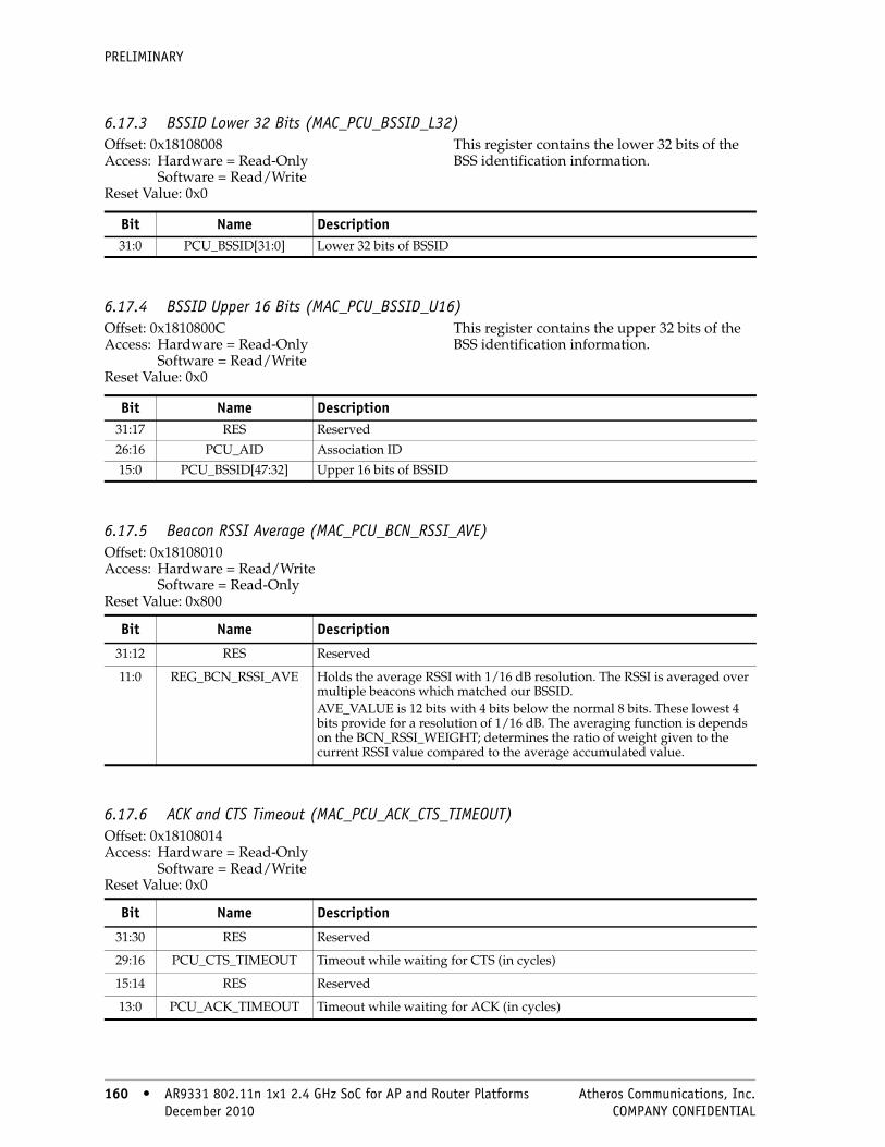
PRELIMINARY
6.17.3 BSSID Lower 32 Bits (MAC_PCU_BSSID_L32)Offset: 0x18108008Access: Hardware = Read-Only
Software = Read/WriteReset Value: 0x0
This register contains the lower 32 bits of the BSS identification information.
6.17.4 BSSID Upper 16 Bits (MAC_PCU_BSSID_U16)Offset: 0x1810800CAccess: Hardware = Read-Only
Software = Read/WriteReset Value: 0x0
This register contains the upper 32 bits of the BSS identification information.
6.17.5 Beacon RSSI Average (MAC_PCU_BCN_RSSI_AVE)Offset: 0x18108010Access: Hardware = Read/Write
Software = Read-OnlyReset Value: 0x800
BCN_RSSI_AVE
6.17.6 ACK and CTS Timeout (MAC_PCU_ACK_CTS_TIMEOUT)Offset: 0x18108014Access: Hardware = Read-Only
Software = Read/WriteReset Value: 0x0
Bit Name Description31:0 PCU_BSSID[31:0] Lower 32 bits of BSSID
Bit Name Description31:17 RES Reserved
26:16 PCU_AID Association ID
15:0 PCU_BSSID[47:32] Upper 16 bits of BSSID
Bit Name Description
31:12 RES Reserved
11:0 REG_BCN_RSSI_AVE Holds the average RSSI with 1/16 dB resolution. The RSSI is averaged over multiple beacons which matched our BSSID. AVE_VALUE is 12 bits with 4 bits below the normal 8 bits. These lowest 4 bits provide for a resolution of 1/16 dB. The averaging function is depends on the BCN_RSSI_WEIGHT; determines the ratio of weight given to the current RSSI value compared to the average accumulated value.
Bit Name Description
31:30 RES Reserved
29:16 PCU_CTS_TIMEOUT Timeout while waiting for CTS (in cycles)
15:14 RES Reserved
13:0 PCU_ACK_TIMEOUT Timeout while waiting for ACK (in cycles)
160 • AR9331 802.11n 1x1 2.4 GHz SoC for AP and Router Platforms Atheros Communications, Inc. 160 • December 2010 COMPANY CONFIDENTIAL

PRELIMINARY
6.17.7 Beacon RSSI Control (MAC_PCU_BCN_RSSI_CTL)Offset: 0x18108018Access: Hardware = Read-Only
Software = Read/WriteReset Value: 0x0
6.17.8 Ms Counter and Rx/Tx Latency (MAC_PCU_USEC_LATENCY)Offset: 0x1810801CAccess: Hardware = Read-Only
Software = Read/WriteReset Value: 0x0
6.17.9 Reset TSF (MAC_PCU_RESET_TSF)Offset: 0x18108020Access: Hardware = Read/Write
Software = Read/WriteReset Value: 0x0
Controls beacon operation by the PCU.
Bit Name Description
31:30 RES Reserved
29 REG_BCN_RSSI_RST_STROBE
The BCN_RSSI_RESET clears “BCN_RSSI_AVE” to aid in changing channels
28:24 REG_BCN_RSSI_WEIGHT Used to calculate “BCN_RSSI_AVE”
23:16 RES Reserved
15:8 PCU_BCN_MISS_THR Threshold at which the beacon miss interrupt asserts. Because the beacon miss counter increments at TBTT, it increments to 1 before the first beacon.
7:0 PCU_RSSI_THR The threshold at which the beacon low RSSI interrupt is asserted when the average RSSI (“BCN_RSSI_AVE”) below this level
Bit Name Description
31:29 RES Reserved
28:23 PCU_RXDELAY Baseband Rx latency to start of SIGNAL (in μs)
22:14 PCU_TXDELAY Baseband Tx latency to start of timestamp in beacon frame (in μs)
13:0 RES Reserved
Bit Name Description
31:26 RES Reserved
25 ONE_SHOT Setting this bit causes the TSF2 to reset. This register clears immediately after reset.
24 ONE_SHOT Setting this bit causes the TSF to reset. This register clears immediately after reset.
23:0 RES Reserved
Atheros Communications, Inc. AR9331 802.11n 1x1 2.4 GHz SoC for AP and Router Platforms • 161 COMPANY CONFIDENTIAL December 2010 • 161

PRELIMINARY
162 • AR9331 802.11n 1x1 2.4 GHz SoC for AP and Router Platforms Atheros Communications, Inc.
6.17.10 Maximum CFP Duration (MAC_PCU_MAX_CFP_DUR)Offset: 0x18108038 Access:Hardware = Read-Only Software = Read/Write Reset Value: 0x0
This register contains the maximum time for a CFP.
6.17.11 Rx Filter (MAC_PCU_RX_FILTER)Offset: 0x1810803CAccess: Hardware = Read-Only
Software = Read/WriteReset Value: 0x0
This register determines Rx frame filtering.
NOTE: If any bit is set, the corresponding packet types pass the filter and DMA. All filter conditions except the promiscuous setting rely on the no early PHY error and protocol version being checked to ensure it is version 0.
Bit Name Description
31:28 RES Reserved
27 USEC_FRAC_DENOMINATOR[27:24]
See description for the MAC_PCU_USEC_LATENCY register bit USEC
23:20 RES Reserved
16:16 USEC_FRAC_DENOMINATOR[19:16]
See description for the MAC_PCU_USEC_LATENCY register bit USEC
15:0 VALUE[15:0] Maximum contention free period duration (in μs)
Bit Name Description31:19 RES Reserved
18 MGMT_ACTION_MCAST Enable receive of multicast frames for management action frames
17 HW_BCN_PROC_ENABLE
If set, the beacon frame with matching BSSID is filtered per hardware beacon processing logic. See the HW_BCN_PROC register.
16 RST_DLMTR_CNT_DISABLE
Clearing this bit resets the ST_DLMTR_CNT to 0 when RXSM.STATE leaves the START_DELIMITER state.
15 MCAST_BCAST_ALL Enables receipt of all multicast and broadcast frames
14 PS_POLL Enables receipt of PS-POLL
13:10 RES Reserved
9 MY_BEACON Retrieves any beacon frame with matching SSID
8 RES Reserved
7 PROBE_REQ Probe request enable; enables reception of all probe request frames
6 RES Reserved
5 PROMISCUOUS Promiscuous Rx enable; enables reception of all frames, including errors
4 BEACON Beacon frame enable; enables reception of beacon frames.
3 CONTROL Control frame enable; enables reception of control frames
2 BROADCAST Broadcast frame enable; enables reception of non beacon broadcast frames that originate from the BSS whose ID matches BSSID
1 MULTICAST Multicast frame enable; enables reception of multicast frames that match the multicast filter
0 UNICAST Unicast frame enable; enables reception of unicast (directed) frames that match the STA address
162 • December 2010 COMPANY CONFIDENTIAL

PRELIMINARY
6.17.12 Multicast Filter Mask Lower 32 Bits (MAC_PCU_MCAST_FILTER_L32)Offset: 0x18108040 Access: Hardware = Read-Only
Software = Read/WriteReset Value: 0x0
6.17.13 Multicast Filter Mask Upper 32 Bits (MAC_PCU_MCAST_FILTER_U32)Offset: 0x18108044 Access: Hardware = Read-Only
Software = Read/WriteReset Value: 0x0
6.17.14 Diagnostic Switches (MAC_PCU_DIAG_SW)Offset: 0x18108048 Access: Hardware = Read-Only
Software = Read/WriteReset Value: 0x0
Controls the operation of the PCU, including enabling/disabling acknowledgements, CTS, transmission, reception, encryption, loopback, FCS, channel information, and scrambler seeds.
Bit Name Description31:0 PCU_MCAST_MASK Multicast filter mask low. Lower 32 bits of multicast filter mask.
Bit Name Description
31:0 PCU_MCAST_MASK Multicast filter mask high. Upper 32 bits of multicast filter mask.
Bit Name Description
31:30 RES Reserved
29 RX_CLEAR_EXT_LOW Force the RX_CLEAR_EXT signal to appear to the MAC as being low
28 RX_CLEAR_CTL_LOW Force the RX_CLEAR_CTL signal to appear to the MAC as being low
27 RES Reserved
26 SATURATE_CYCLE_CNT The saturate cycle count bit, if set, causes the “Cycle Counter (MAC_PCU_CYCLE_CNT)” register to saturate instead of shifting to the right by 1 every time the count reaches 0xFFFFFFFF. This saturate condition also holds the RX_CLEAR, RX_FRAME, and TX_FRAME counts.
25 FORCE_RX_ABORT Force Rx abort bit in conjunction with Rx block aids quick channel change to shut down Rx. The force Rx abort bit kills with the Rx_abort any frame currently transferring between the MAC and baseband. while the RX block bit prevents any new frames from getting started.
24:23 RES Reserved
22 CHAN_IDLE_HIGH Force channel idle high
21 IGNORE_NAV Ignore virtual carrier sense (NAV)
20 RX_CLEAR_HIGH Force RX_CLEAR high
19:18 RES Reserved
17 ACCEPT_NON_V0 Enable or disable protocol field
16:7 RES Reserved
6 LOOP_BACK Enable or disable Tx data loopback
5 HALT_RX Enable or disable reception
Atheros Communications, Inc. AR9331 802.11n 1x1 2.4 GHz SoC for AP and Router Platforms • 163 COMPANY CONFIDENTIAL December 2010 • 163

PRELIMINARY
6.17.15 TSF Lower 32 Bits (MAC_PCU_TSF_L32)Offset: 0x1810804CAccess: Hardware = Read/Write
Software = Read/WriteReset Value: 0xFFFFFFF
6.17.16 TSF Upper 32 Bits (MAC_PCU_TSF_U32)Offset: 0x18108050Access: Hardware = Read/Write
Software = Read/WriteReset Value: 0xFFFFFFF
6.17.17 AES Mute Mask 0 (MAC_PCU_AES_MUTE_MASK_0)Offset: 0x1810805CAccess: Hardware = Read-Only
Software = Read/WriteReset Value: See Field Description
4 NO_DECRYPT Enable or disable decryption
3 NO_ENCRYPT Enable or disable encryption
2 NO_CTS Enable or disable CTS generation
1 NO_ACK Enable or disable acknowledgement generation for all frames
0 PCU_INVALKEY_NOACK Enable or disable acknowledgement when a valid key is not found for the received frames in the key cache.
Bit Name Description
Bit Name Description
31:0 VALUE The timestamp value in μsWrites to this register do not cause the TSF to change. Rather, the value is held in a temporary staging area until this register is written, at which point both the lower and upper parts of the TSF are loaded. A read result of 0xFFFFFFFF indicates that the read occurred before TSF logic came out of sleep. It may take up to 45 μs after the chip is brought out of sleep for the TSF logic to wake.
Bit Name Description
31:0 VALUE The timestamp value in μs
Bit Name Reset Description
31:16 QOS_MUTEMASK 0xFFFF AES mute mask for TID field
15:0 FC_MUTEMASK 0x478F AES mute mask for frame control field
164 • AR9331 802.11n 1x1 2.4 GHz SoC for AP and Router Platforms Atheros Communications, Inc. 164 • December 2010 COMPANY CONFIDENTIAL

PRELIMINARY
6.17.18 AES Mute Mask 1(MAC_PCU_AES_MUTE_MASK_1)Offset: 0x18108060Access: Hardware = Read-Only
Software = Read/WriteReset Value: See Field Description
6.17.19 Last Rx Beacon TSF (MAC_PCU_LAST_BEACON_TSF)Offset: 0x18108080Access: Hardware = Write-only
Software = Read-OnlyReset Value: 0x0
This threshold register indicates the minimum amount of data required before initiating a transmission.
6.17.20 Current NAV (MAC_PCU_NAV)Offset: 0x18108084Access: Hardware = Read/Write
Software = Read/WriteReset Value: 0x0
6.17.21 Successful RTS Count (MAC_PCU_RTS_SUCCESS_CNT)Offset: 0x18108088Access: Hardware = Read/Write
Software = Read-OnlyReset Value: 0x0
This register counts the number of successful RTS exchanges. The counter stops at 0xFFFF. After a read, automatically resets to 0.
6.17.22 Failed RTS Count (MAC_PCU_RTS_FAIL_CNT)Offset: 0x1810808CAccess: Hardware = Read/Write
Software = Read-OnlyReset Value: 0x0
This register counts the number of failed RTS exchanges. The counter stops at 0xFFFF. After a read, this register is automatically reset to 0.
Bit Name Reset Description
31:16 FC_MGMT 0xE7FF AES mute mask for management frame control field
15:0 SEQ_MUTEMASK 0x000F AES mute mask for sequence number field
Bit Name Description
31:0 LAST_TSTP Beacon timestamp. Lower 32 bits of timestamp of the last beacon received.
Bit Name Description
31:26 RES Reserved
25:0 CS_NAV Current NAV value (in μs)
Bit Name Description
31:16 RES Reserved
15:0 RTS_OK RTS/CTS exchange success counter
Bit Name Description
31:16 RES Reserved
15:0 RTS_FAIL RTS/CTS exchange failure counter
Atheros Communications, Inc. AR9331 802.11n 1x1 2.4 GHz SoC for AP and Router Platforms • 165 COMPANY CONFIDENTIAL December 2010 • 165

PRELIMINARY
6.17.23 FAIL ACK Count (MAC_PCU_ACK_FAIL_CNT)Offset: 0x18108090Access: Hardware = Read/Write
Software = Read-OnlyReset Value: 0x0
This register counts the number of failed acknowledgements. The counter stops at 0xFFFF. After a read, this register is automatically reset to 0.
6.17.24 Failed FCS Count (MAC_PCU_FCS_FAIL_CNT)Offset: 0x18108094Access: Hardware = Read/Write
Software = Read-OnlyReset Value: 0x0
This register counts the number of failed frame check sequences. The counter stops at 0xFFFF. After a read, this register is automatically reset to 0.
6.17.25 Beacon Count (MAC_PCU_BEACON_CNT)Offset: 0x18108098Access: Hardware = Read/Write
Software = Read-OnlyReset Value: 0x0
This register counts the number of valid beacon frames received. The counter stops at 0xFFFF. After a read, automatically resets to 0.
6.17.26 Sleep 1 (MAC_PCU_SLP1)Offset: 0x181080D4Access: Hardware = Read/Write
Software = Read-OnlyReset Value: 0x0
The Sleep 1 register in conjunction with the “Sleep 2 (MAC_PCU_SLP2)” register, controls when the AR9331 should wake when waiting for AP Rx traffic. Sleep registers are only used when the AR9331 is in STA mode.
Bit Name Description
31:16 RES Reserved
15:0 ACK_FAIL DATA/ACK failure counter
Bit Name Description
31:16 RES Reserved
15:0 FCS_FAIL FCS failure counter
Bit Name Description
31:16 RES Reserved
15:0 BEACONCNT Valid beacon counter
Bit Name Reset Description31:21 CAB_TIMEOUT 0x5 Time in 1/8 TU the PCU waits for CAB after receiving the beacon or the
previous CAB; insures that if no CAB is received after the beacon or if a long gap occurs between CABs, CAB powersave state returns to idle.
20 RES 0x0 Reserved
19 ASSUME_DTIM 0x0 A mode bit which indicates whether to assume a beacon was missed when the SLP_BEACON_TIMEOUT occurs with no received beacons, in which case is assumes the DTIM was missed, and waits for CAB.
18:0 RES 0x0 Reserved
166 • AR9331 802.11n 1x1 2.4 GHz SoC for AP and Router Platforms Atheros Communications, Inc. 166 • December 2010 COMPANY CONFIDENTIAL

PRELIMINARY
6.17.27 Sleep 2 (MAC_PCU_SLP2)Offset: 0x181080D8Access: Hardware = Read/Write
Software = Read-OnlyReset Value: 0x2
6.17.28 Address 1 Mask Lower 32 Bits (MAC_PCU_ADDR1_MASK_L32)Offset: 0x181080E0Access: Hardware = Read-Only
Software = Read/WriteReset Value: 0xFFFFFFFF
This STA register provides multiple BSSID support when the AR9331 is in AP mode.
6.17.29 Address 1 Mask Upper 16 Bits (MAC_PCU_ADDR1_MASK_U16)Offset: 0x181080E4Access: Hardware = Read-Only
Software = Read/WriteReset Value: 0xFFFF
This STA register provides multiple BSSID support when the AR9331 is in AP mode.
6.17.30 Tx Power Control (MAC_PCU_TPC)Offset: 0x181080E8Access: Hardware = Read-Only
Software = Read/WriteReset Value: 0x3F
The 6-bit Tx power control sent from the MAC to the baseband is typically controlled using the Tx descriptor field. But self-generated response frames such as ACK, CTS, and chirp that do not have a Tx descriptor use the values in the Tx power control register instead.
Bit Name Description31:21 BEACON_TIMEOUT Time in TU that the PCU waits for a beacon after waking up. If this time
expires, the PCU woke due to SLP_NEXT_DTIM, and SLP_ASSUME_DTIM is active, then it assumes the beacon was missed and goes directly to watching for CAB. Otherwise when this time expires, the beacon powersave state returns to idle.
20:0 RES Reserved
Bit Name Description31:0 STA_MASK_L STA address mask lower 32-bit register. Provides multiple BSSID support.
Bit Name Description31:16 RES Reserved
15:0 STA_MASK_L STA address mask upper 16-bit register. Provides multiple BSSID support.
Bit Name Description31:30 RES Reserved
29:24 RPT_PWR Tx power control for self-generated action/NoACK frame
23:22 RES Reserved
21:16 CHIRP_PWR Tx power control for chirp
15:14 RES Reserved
13:8 CTS_PWR Tx power control for CTS
7:6 RES Reserved
5:0 ACK_PWR Tx power control for ACK
Atheros Communications, Inc. AR9331 802.11n 1x1 2.4 GHz SoC for AP and Router Platforms • 167 COMPANY CONFIDENTIAL December 2010 • 167
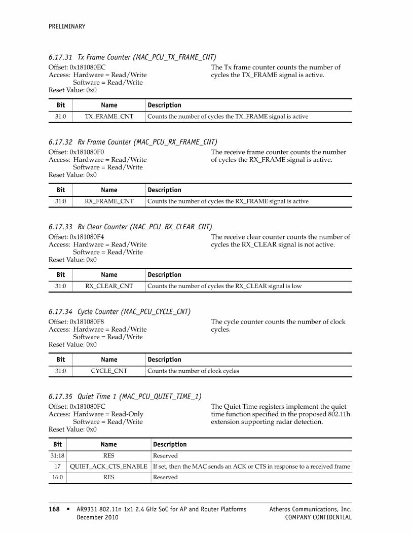
PRELIMINARY
6.17.31 Tx Frame Counter (MAC_PCU_TX_FRAME_CNT)Offset: 0x181080ECAccess: Hardware = Read/Write
Software = Read/WriteReset Value: 0x0
The Tx frame counter counts the number of cycles the TX_FRAME signal is active.
6.17.32 Rx Frame Counter (MAC_PCU_RX_FRAME_CNT)Offset: 0x181080F0Access: Hardware = Read/Write
Software = Read/WriteReset Value: 0x0
The receive frame counter counts the number of cycles the RX_FRAME signal is active.
6.17.33 Rx Clear Counter (MAC_PCU_RX_CLEAR_CNT)Offset: 0x181080F4Access: Hardware = Read/Write
Software = Read/WriteReset Value: 0x0
The receive clear counter counts the number of cycles the RX_CLEAR signal is not active.
6.17.34 Cycle Counter (MAC_PCU_CYCLE_CNT)Offset: 0x181080F8Access: Hardware = Read/Write
Software = Read/WriteReset Value: 0x0
The cycle counter counts the number of clock cycles.
6.17.35 Quiet Time 1 (MAC_PCU_QUIET_TIME_1)Offset: 0x181080FCAccess: Hardware = Read-Only
Software = Read/WriteReset Value: 0x0
The Quiet Time registers implement the quiet time function specified in the proposed 802.11h extension supporting radar detection.
Bit Name Description
31:0 TX_FRAME_CNT Counts the number of cycles the TX_FRAME signal is active
Bit Name Description
31:0 RX_FRAME_CNT Counts the number of cycles the RX_FRAME signal is active
Bit Name Description
31:0 RX_CLEAR_CNT Counts the number of cycles the RX_CLEAR signal is low
Bit Name Description
31:0 CYCLE_CNT Counts the number of clock cycles
Bit Name Description
31:18 RES Reserved
17 QUIET_ACK_CTS_ENABLE If set, then the MAC sends an ACK or CTS in response to a received frame
16:0 RES Reserved
168 • AR9331 802.11n 1x1 2.4 GHz SoC for AP and Router Platforms Atheros Communications, Inc. 168 • December 2010 COMPANY CONFIDENTIAL

PRELIMINARY
6.17.36 Quiet Time 2 (MAC_PCU_QUIET_TIME_2)Offset: 0x18108100Access: Hardware = Read-Only
Software = Read/WriteReset Value: 0x0
The Quiet Time registers implement the quiet time function specified in the proposed 802.11h extension supporting radar detection.
NOTE: QUIET_ENABLE is implemented as GENERIC_TIMER_ENABLE and NEXT_QUIET as GENERIC_TIMER_NEXT. QUIET_PERIOD is implemented as GENERIC_TIMER_PERIOD.
6.17.37 QoS NoACK (MAC_PCU_QOS_NO_ACK)Offset: 0x18108108Access: Hardware = Read-Only
Software = Read/WriteReset Value: 0x52
This register provides a mechanism to locate the NoACK information in the QoS field and determine which encoding means NoACK.
Bit Name Description
31:16 QUIET_DURATION The length of time in TUs (TU = 1024 μs) that the chip is required to be quiet
15:0 RES Reserved
Bit Name Description
31:9 RES Reserved
8:7 NOACK_BYTE_OFFSET Number of bytes from the byte after end of the header of a data packet to the byte location where NoACK information is stored. (The end of the header is at byte offset 25 for 3-address packets and 31 for 4-address packets.)
6:4 NOACK_BIT_OFFSET Offsets from the byte where the NoACK information should be stored; offset can range from 0 to 6 only
3:0 NOACK_2_BIT_VALUES
These values are of a two bit field that indicate NoACK
NOACK_2_BIT_VALUE Encoding Matching NoACK
xxx1 00
xx1x 01
x1xx 10
1xxx 11
Atheros Communications, Inc. AR9331 802.11n 1x1 2.4 GHz SoC for AP and Router Platforms • 169 COMPANY CONFIDENTIAL December 2010 • 169

PRELIMINARY
6.17.38 PHY Error Mask (MAC_PCU_PHY_ERROR_MASK)Offset: 0x1810810CAccess: Hardware = Read-Only
Software = Read/WriteReset Value: 0x2
NOTE: Provides the ability to choose which PHY errors from the baseband to filter. The error number offsets into this register. If the mask value at the offset is 0, this error filters and does not show up on the Rx queue.
6.17.39 Rx Buffer (MAC_PCU_RXBUF)Offset: 0x18108114Access: Hardware = Read-Only
Software = Read/WriteReset Value: See Field Description
Bit Name Description
31 ERROR CCK RESTART CCK restart error
30 ERROR CCK SERVICE CCK service error
29:28 RES Reserved
27 ERROR CCK RATE_ILLEGAL CCK illegal rate error
26 ERROR CCK HEADER_CRC CCK CRC header error
25 ERROR CCK TIMING False detection for CCK
24 RES Reserved
23 ERROR OFDM RESTART OFDM restart error
22 ERROR OFDM SERVICE OFDM service error
21 ERROR OFDM POWER_DROP OFDM power drop error
20 ERROR OFDM LENGTH_ILLEGAL OFDM illegal length error
19 ERROR OFDM RATE_ILLEGAL OFDM illegal rate error
18 ERROR OFDM SIGNAL_PARITY OFDM signal parity error
17 ERROR OFDM TIMING False detection for OFDM
16:8 RES Reserved
7 ERROR TX_INTERRUPT_RX Transmit interrupt
6 ERROR ABORT Abort error
5 ERROR RADAR_DETECT Radar detect error
4 ERROR PANIC Panic error
3:1 RES Reserved
0 ERROR TRANSMIT_UNDERRUN Transmit underrun error
Bit Name Reset Description
31:12 RES 0x0 Reserved
11 REG_RD_ENABLE
0x0 When reading MAC_PCU_BUF with this bit set, hardware returns the contents of the receive buffer.
10:0 HIGH_PRIORITY_THRSHD
0x7FF When number of valid entries in the receive buffer is larger than this threshold, the host interface logic gives the higher priority to receive side to prevent receive buffer overflow.
170 • AR9331 802.11n 1x1 2.4 GHz SoC for AP and Router Platforms Atheros Communications, Inc. 170 • December 2010 COMPANY CONFIDENTIAL
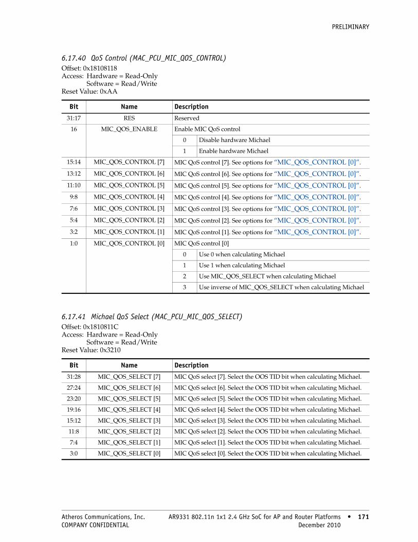
PRELIMINARY
6.17.40 QoS Control (MAC_PCU_MIC_QOS_CONTROL)Offset: 0x18108118Access: Hardware = Read-Only
Software = Read/WriteReset Value: 0xAA
6.17.41 Michael QoS Select (MAC_PCU_MIC_QOS_SELECT)Offset: 0x1810811CAccess: Hardware = Read-Only
Software = Read/WriteReset Value: 0x3210
Bit Name Description
31:17 RES Reserved
16 MIC_QOS_ENABLE Enable MIC QoS control
0 Disable hardware Michael
1 Enable hardware Michael
15:14 MIC_QOS_CONTROL [7] MIC QoS control [7]. See options for “MIC_QOS_CONTROL [0]”.
13:12 MIC_QOS_CONTROL [6] MIC QoS control [6]. See options for “MIC_QOS_CONTROL [0]”.
11:10 MIC_QOS_CONTROL [5] MIC QoS control [5]. See options for “MIC_QOS_CONTROL [0]”.
9:8 MIC_QOS_CONTROL [4] MIC QoS control [4]. See options for “MIC_QOS_CONTROL [0]”.
7:6 MIC_QOS_CONTROL [3] MIC QoS control [3]. See options for “MIC_QOS_CONTROL [0]”.
5:4 MIC_QOS_CONTROL [2] MIC QoS control [2]. See options for “MIC_QOS_CONTROL [0]”.
3:2 MIC_QOS_CONTROL [1] MIC QoS control [1]. See options for “MIC_QOS_CONTROL [0]”.
1:0 MIC_QOS_CONTROL [0] MIC QoS control [0]
0 Use 0 when calculating Michael
1 Use 1 when calculating Michael
2 Use MIC_QOS_SELECT when calculating Michael
3 Use inverse of MIC_QOS_SELECT when calculating Michael
Bit Name Description
31:28 MIC_QOS_SELECT [7] MIC QoS select [7]. Select the OOS TID bit when calculating Michael.
27:24 MIC_QOS_SELECT [6] MIC QoS select [6]. Select the OOS TID bit when calculating Michael.
23:20 MIC_QOS_SELECT [5] MIC QoS select [5]. Select the OOS TID bit when calculating Michael.
19:16 MIC_QOS_SELECT [4] MIC QoS select [4]. Select the OOS TID bit when calculating Michael.
15:12 MIC_QOS_SELECT [3] MIC QoS select [3]. Select the OOS TID bit when calculating Michael.
11:8 MIC_QOS_SELECT [2] MIC QoS select [2]. Select the OOS TID bit when calculating Michael.
7:4 MIC_QOS_SELECT [1] MIC QoS select [1]. Select the OOS TID bit when calculating Michael.
3:0 MIC_QOS_SELECT [0] MIC QoS select [0]. Select the OOS TID bit when calculating Michael.
Atheros Communications, Inc. AR9331 802.11n 1x1 2.4 GHz SoC for AP and Router Platforms • 171 COMPANY CONFIDENTIAL December 2010 • 171

PRELIMINARY
6.17.42 Miscellaneous Mode (MAC_PCU_MISC_MODE)
Offset: 0x18108120Access: Hardware = Read-Only
Software = Read/WriteReset Value: See Field Description
Bit Name Reset Description31:29 RES 0x0 Reserved
28 ALWAYS_PERFORM_
KEY_SEARCH
0x0 If this bit is set, key search is performed for every frame in an aggregate. If this bit is cleared, key search is only performed for the first frame of an aggregate. Unless the transmitter address is different between the frames in an aggregate. This bit has no effect on non-aggregate frame packets.
27 SEL_EVM 0x1 If the SEL_EVM bit is set, the evm field of the Rx descriptor status contains the EVM data received from the baseband. If this bit is cleared, the evm field of the Rx descriptor status contains 3 bytes of Legacy PLCP, 2 service bytes, and 6 bytes of HP PLCP.
26 CLEAR_BA_VALID 0x0 If the CLEAR_BA_VALID bit is set, the state of the block ACK storage is invalidated.
25:22 RES 0x0 Reserved
21 TBTT_PROTECT 0x1 If the TBTT_PROTECT bit is set, then the time from TBTT to 20 μs after TBTT is protected from transmit. Turn this off in ad hoc mode or if this MAC is used in the AP.
20 BT_ANT_PREVENTS_RX
0x1 Prevents Rx of new frames when the BT has control over the antenna, primarily to simplify verification. Even when the antenna is switched over to the BT device, if the WLAN receive frame RSSI is strong it may still be received although attenuated significantly. Setting this bit will prevent this frame from entering the Rx path.
19 RES 0x0 Reserved
18 FORCE_QUIET_COLLISION
0x0 If the FORCE_QUIET_COLLISION bit is set, the PCU thinks that it is in quiet collision period, kills any transmit frame in progress, and prevents any new frame from starting.
17:13 RES 0x0 Reserved
12 TXOP_TBTT_LIMIT_ENABLE
0x0 If this limit is set, then logic to limit the value of the duration to fit the time remaining in TXOP and time remaining until TBTT is turned on. This logic will also filter frames, which will exceed TXOP.
11:5 RES 0x0 Reserved
4 CCK_SIFS_MODE 0x0 If the CCK_SIFS_MODE is set, the chip assumes that it is using 802.11g mode where SIFS is set to 10 μs and non-CCK frames must add 6 to SIFS to make it CCK frames. This bit is needed in the duration calculation, which also needs the SIFS_TIME register.
3 TX_ADD_TSF 0x0 If the TX_ADD_TSF bit is set, the TSF in the transmit packet will be added to the internal TSF value for transmit beacons and prob_response frames.
2 MIC_NEW_LOCATION_ENABLE
0x0 If MIC_NEW_LOCATION_ENABLE is set, the Tx Michael Key is assumed to be co-located in the same entry that the Rx Michael key is located.
1 RES 0x0 Reserved
0 BSSID_MATCH_FORCE
0x0 If the BSSID_MATCH_FORCE bit is set, all logic based on matching the BSSID thinks that the BSSID matches.
172 • AR9331 802.11n 1x1 2.4 GHz SoC for AP and Router Platforms Atheros Communications, Inc. 172 • December 2010 COMPANY CONFIDENTIAL

PRELIMINARY
6.17.43 Filtered OFDM Counter (MAC_PCU_FILTER_OFDM_CNT)
Offset: 0x18108124Access: Hardware = Read/Write
Software = Read/WriteReset Value: 0x0
The filtered OFDM counters use the MIB control signals.
6.17.44 Filtered CCK Counter (MAC_PCU_Filter_CCK_CNT)
Offset: 0x18108128Access: Hardware = Read/Write
Software = Read/WriteReset Value: 0x0
6.17.45 PHY Error Counter 1 (MAC_PCU_PHY_ERR_CNT_1)
Offset: 0x1810812CAccess: Hardware = Read/Write
Software = Read/WriteReset Value: 0x0
The PHY error counters count any PHY error matching the respective mask. The bits of 32-bit
masks correspond to the first 32 encoded values of the error. Setting multiple bits in the mask provides an ORing function to provide flexibility in counting. For example, if setting the mask bits to 0xFF0000FF, then all PHY errors from 0–7 and 24–31 are counted.
Bit Name Description
31:24 RES Reserved
23:0 FILTOFDM_CNT Counts the OFDM frames that were filtered using MIB control signals. The MIB freeze register holds all the values of these registers, and MIB zeros out all the values of these registers. PIB MIB forces incrementation of all registers in each cycle. This counter saturates at the highest value and is writable. If the upper two bits of these counters are b11, PCU_MIB_THRESHOLD is asserted and an interrupt generated.
Bit Name Description
31:24 RES Reserved
23:0 FILTCCK_CNT Counts the CCK frames that were filtered using MIB control signals. The MIB freeze register holds all the values of these registers, and MIB zeros out all the values of these registers. PIB MIB forces incrementation of all registers in each cycle. This counter saturates at the highest value and is writable. If the upper two bits of these counters are b11, PCU_MIB_THRESHOLD is asserted and an interrupt generated.
Bit Name Description
31:24 RES Reserved
23:0 PHY_ERROR_CNT1 Counts any PHY error1 using MIB control signals. The MIB freeze register holds all the values of these registers, and MIB zeros out all the values of these registers. PIB MIB forces incrementation of all registers in each cycle. Counter saturates at the highest value and is writable. If the upper two counter bits are b11, PCU_MIB_THRESHOLD is asserted and an interrupt generated.
Atheros Communications, Inc. AR9331 802.11n 1x1 2.4 GHz SoC for AP and Router Platforms • 173 COMPANY CONFIDENTIAL December 2010 • 173
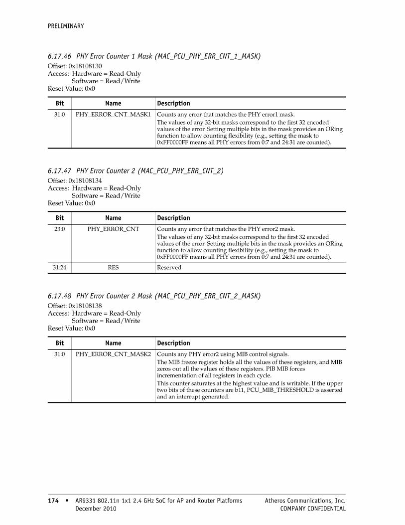
PRELIMINARY
6.17.46 PHY Error Counter 1 Mask (MAC_PCU_PHY_ERR_CNT_1_MASK)Offset: 0x18108130Access: Hardware = Read-Only
Software = Read/WriteReset Value: 0x0
6.17.47 PHY Error Counter 2 (MAC_PCU_PHY_ERR_CNT_2)Offset: 0x18108134Access: Hardware = Read-Only
Software = Read/WriteReset Value: 0x0
6.17.48 PHY Error Counter 2 Mask (MAC_PCU_PHY_ERR_CNT_2_MASK)Offset: 0x18108138Access: Hardware = Read-Only
Software = Read/WriteReset Value: 0x0
Bit Name Description
31:0 PHY_ERROR_CNT_MASK1 Counts any error that matches the PHY error1 mask.The values of any 32-bit masks correspond to the first 32 encoded values of the error. Setting multiple bits in the mask provides an ORing function to allow counting flexibility (e.g., setting the mask to 0xFF0000FF means all PHY errors from 0:7 and 24:31 are counted).
Bit Name Description
23:0 PHY_ERROR_CNT Counts any error that matches the PHY error2 mask.The values of any 32-bit masks correspond to the first 32 encoded values of the error. Setting multiple bits in the mask provides an ORing function to allow counting flexibility (e.g., setting the mask to 0xFF0000FF means all PHY errors from 0:7 and 24:31 are counted).
31:24 RES Reserved
Bit Name Description
31:0 PHY_ERROR_CNT_MASK2 Counts any PHY error2 using MIB control signals. The MIB freeze register holds all the values of these registers, and MIB zeros out all the values of these registers. PIB MIB forces incrementation of all registers in each cycle. This counter saturates at the highest value and is writable. If the upper two bits of these counters are b11, PCU_MIB_THRESHOLD is asserted and an interrupt generated.
174 • AR9331 802.11n 1x1 2.4 GHz SoC for AP and Router Platforms Atheros Communications, Inc. 174 • December 2010 COMPANY CONFIDENTIAL

PRELIMINARY
6.17.49 TSF Threshold (MAC_PCU_TSF_THRESHOLD)Offset: 0x1810813CAccess: Hardware = Read-Only
Software = Read/WriteReset Value: 0xFFFF
6.17.50 PHY Error EIFS Mask (MAC_PCU_PHY_ERROR_EIFS_MASK)Offset: 0x18108144Access: Hardware = Read-Only
Software = Read/WriteReset Value: 0x0
6.17.51 PHY Error Counter 3 (MAC_PCU_PHY_ERR_CNT_3)Offset: 0x18108168Access: Hardware = Read-Only
Software = Read/WriteReset Value: 0x0
6.17.52 PHY Error Counter 3 Mask (MAC_PCU_PHY_ERR_CNT_3_MASK)Offset: 0x1810816CAccess: Hardware = Read-Only
Software = Read/WriteReset Value: 0x0
Bit Name Description
15:0 TSF_THRESHOLD Asserts the PCU_TSF_OUT_OF_RANGE_INTER if the corrected receive TSF in a beacon is different from the internal TSF by more than this threshold.
31:16 RES Reserved
Bit Name Description
31:0 VALUE This mask provides the ability to choose which PHY errors from the baseband cause EIFS delay. The error number is used as an offset into this mask. If the mask value at the offset is 1, then this error will not cause EIFS delay.
Bit Name Description
23:0 PHY_ERROR_CNT3 Count of PHY errors that pass the PHY_ERR_CNT_3_MASK filter
31:24 RES Reserved
Bit Name Description
31:0 PHY_ERROR_CNT_MASK3
Mask of the PHY error number allowed to be counted
Atheros Communications, Inc. AR9331 802.11n 1x1 2.4 GHz SoC for AP and Router Platforms • 175 COMPANY CONFIDENTIAL December 2010 • 175

PRELIMINARY
6.17.53 Bluetooth Mode (MAC_PCU_BLUETOOTH_MODE)Offset: 0x18108170 Access: Read/Write Reset Value: See Field Description
6.17.54 Bluetooth WL_LEVEL (MAC_PCU_BLUETOOTH_WL_WEIGHTS0)Offset: 0x18108174 Access: Read/Write Reset Value: 0x33332210
Bit Name Reset Description
31:24 FIRST_SLOT_TIME 0x18 Time from the rising edge of BT_ACTIVE to the time in μs when BT_PRIORITY is sampled as the Tx/Rx and BT_FREQ are sampled.
23:18 PRIORITY_TIME 0x12 Used in the slotted mode (BT_MODE = 0x2) to indicate the time in μs from the rising edge or BT_ACTIVE to when BT_PRIORITY can be sampled to indicate priority
17 WL_ACTIVE_POLARITY
0x0 When this bit is high, WL_ACTIVE is active low. When this bit is low, WL_ACTIVE is active high.
16:13 QCU_THRESH 0x3 Indicates which QCUs should be considered high priority. Any QCU number > QCU_THRESH is treated as high priority
12 QUIET 0x0 Causes a quiet collision on Tx if the BT device has higher priority
11:10 BT_MODE 0x3 ■ If BT_MODE is 0x0, the device is in legacy RX_CLEAR mode (2-wire mode)
■ If BT_MODE is 0x1, the device is in untimed mode (3-wire mode)■ If BT_MODE is 0x2, the device is in slotted mode (4-wire mode)■ If BT_MODE is 0x3, the device does not support BT coexistence
9 TX_FRAME_EXTEND
0x0 Extends the RX_CLEAR so that as soon as TX_FRAME is asserted at the MAC the RX_CLEAR will drop
8 TX_STATE_EXTEND
0x0 Extends RX_CLEAR as long as TXSM is transmitting or waiting for a response
7:0 TIME_EXTEND 0x0 Extends RX_CLEAR after frame Tx or Rx so that bursts are protected. The value is in μs.
Bit Name Description
31:0 VALUE Creates a level for every WLAN input condition
176 • AR9331 802.11n 1x1 2.4 GHz SoC for AP and Router Platforms Atheros Communications, Inc. 176 • December 2010 COMPANY CONFIDENTIAL
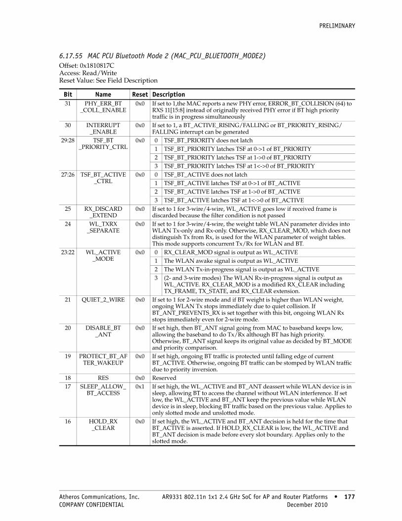
PRELIMINARY
6.17.55 MAC PCU Bluetooth Mode 2 (MAC_PCU_BLUETOOTH_MODE2)Offset: 0x1810817C Access: Read/Write Reset Value: See Field Description
Bit Name Reset Description31 PHY_ERR_BT
_COLL_ENABLE0x0 If set to 1,the MAC reports a new PHY error, ERROR_BT_COLLISION (64) to
RXS 11[15:8] instead of originally received PHY error if BT high priority traffic is in progress simultaneously
30 INTERRUPT_ENABLE
0x0 If set to 1, a BT_ACTIVE_RISING/FALLING or BT_PRIORITY_RISING/FALLING interrupt can be generated
29:28 TSF_BT_PRIORITY_CTRL
0x0 0 TSF_BT_PRIORITY does not latch1 TSF_BT_PRIORITY latches TSF at 0->1 of BT_PRIORITY2 TSF_BT_PRIORITY latches TSF at 1->0 of BT_PRIORITY3 TSF_BT_PRIORITY latches TSF at 1<->0 of BT_PRIORITY
27:26 TSF_BT_ACTIVE_CTRL
0x0 0 TSF_BT_ACTIVE does not latch1 TSF_BT_ACTIVE latches TSF at 0->1 of BT_ACTIVE2 TSF_BT_ACTIVE latches TSF at 1->0 of BT_ACTIVE3 TSF_BT_ACTIVE latches TSF at 1<->0 of BT_ACTIVE
25 RX_DISCARD_EXTEND
0x0 If set to 1 for 3-wire/4-wire, WL_ACTIVE goes low if received frame is discarded because the filter condition is not passed
24 WL_TXRX_SEPARATE
0x0 If set to 1 for 3-wire/4-wire, the weight table WLAN parameter divides into WLAN Tx-only and Rx-only. Otherwise, RX_CLEAR_MOD, which does not distinguish Tx from Rx, is used for the WLAN parameter of weight tables. This mode supports concurrent Tx/Rx for WLAN and BT.
23:22 WL_ACTIVE_MODE
0x0 0 RX_CLEAR_MOD signal is output as WL_ACTIVE1 The WLAN awake signal is output as WL_ACTIVE2 The WLAN Tx-in-progress signal is output as WL_ACTIVE3 (2- and 3-wire modes) The WLAN Rx-in-progress signal is output as
WL_ACTIVE. RX_CLEAR_MOD is a modified RX_CLEAR including TX_FRAME, TX_STATE, and RX_CLEAR extension.
21 QUIET_2_WIRE 0x0 If set to 1 for 2-wire mode and if BT weight is higher than WLAN weight, ongoing WLAN Tx stops immediately due to quiet collision. If BT_ANT_PREVENTS_RX is set together with this bit, ongoing WLAN Rx stops immediately even for 2-wire mode.
20 DISABLE_BT_ANT
0x0 If set high, then BT_ANT signal going from MAC to baseband keeps low, allowing the baseband to do Tx/Rx although BT has high priority. Otherwise, BT_ANT signal keeps its original value as decided by BT_MODE and priority comparison.
19 PROTECT_BT_AFTER_WAKEUP
0x0 If set high, ongoing BT traffic is protected until falling edge of current BT_ACTIVE. Otherwise, ongoing BT traffic can be stomped by WLAN traffic due to priority inversion.
18 RES 0x0 Reserved17 SLEEP_ALLOW_
BT_ACCESS0x1 If set high, the WL_ACTIVE and BT_ANT deassert while WLAN device is in
sleep, allowing BT to access the channel without WLAN interference. If set low, the WL_ACTIVE and BT_ANT keep the previous value while WLAN device is in sleep, blocking BT traffic based on the previous value. Applies to only slotted mode and unslotted mode.
16 HOLD_RX_CLEAR
0x0 If set high, the WL_ACTIVE and BT_ANT decision is held for the time that BT_ACTIVE is asserted. If HOLD_RX_CLEAR is low, the WL_ACTIVE and BT_ANT decision is made before every slot boundary. Applies only to the slotted mode.
Atheros Communications, Inc. AR9331 802.11n 1x1 2.4 GHz SoC for AP and Router Platforms • 177 COMPANY CONFIDENTIAL December 2010 • 177

PRELIMINARY
6.17.56 MAC PCU Generic Timers 2 (MAC_PCU_GENERIC_TIMERS2)Offset: 0x18108180 Access: Read/Write Reset Value: Undefined
6.17.57 MAC PCU Generic Timers Mode 2 (MAC_PCU_GENERIC_TIMERS2_MODE)Offset: 0x181081C0 Access: See Field Description Reset Value: Undefined
6.17.58 MAC PCU BT Coexistence WLAN Weights (MAC_PCU_BLUETOOTH_WL_WEIGHTS1)Offset: 0x181081C4 Access: Read/Write Reset Value: 0x33332210
6.17.59 MAC PCU BT Coexistence TSF Snapshot for BT_ACTIVE (MAC_PCU_BLUETOOTH_TSF_BT_ACTIVE)
Offset: 0x181081C8 Access: Read-Only Reset Value: 0x0
15:8 BCN_MISS_CNT 0x0 This read-only bit gives the count of consecutive missed beacons7:0 BCN_MISS
_THRESH0x0 If > 1, compared to BCN_MISS_CNT. If < BCN_MISS_CNT, the MAC
switches BT_ANT to listen for a beacon until it is received or a timeout occurs. If a beacon timeout occurs, BT_ANT resumes normal behavior until the MAC is waiting for a beacon. If BT_BCN_MISS_THRESH = 0 then the logic is disabled. Applies to both slotted and unslotted modes.
Bit Name Reset Description
Bit Name Description31:0 DATA MAC_PCU_GENERIC_TIMERS
Bit Name Access Description31:11 RES RO Reserved
10:8 OVERFLOW_INDEX RO Overflow index
7:0 ENABLE R/W Enable
Bit Name Description31:0 VALUE Creates a level for every WLAN input condition
Bit Name Description31:0 VALUE Latches TSF at rising/falling/both edges of BT_ACTIVE by control of
TSF_BT_ACTIVE_CTRL of the “MAC PCU Bluetooth Mode 2 (MAC_PCU_BLUETOOTH_MODE2)” register.
178 • AR9331 802.11n 1x1 2.4 GHz SoC for AP and Router Platforms Atheros Communications, Inc. 178 • December 2010 COMPANY CONFIDENTIAL

PRELIMINARY
6.17.60 MAC PCU BT Coexistence TSF Snapshot for BT_PRIORITY (MAC_PCU_BLUETOOTH_TSF_BT_PRIORITY)
Offset: 0x181081CC Access: Read-Only Reset Value: 0x0
6.17.61 SIFS, Tx Latency and ACK Shift (MAC_PCU_TXSIFS)Offset: 0x181081D0Access: Hardware = Read-Only
Software = Read/WriteReset Value: 0x0
6.17.62 MAC PCU Bluetooth Mode 3 (MAC_PCU_BLUETOOTH_MODE3)Offset: 0x181081D4 Access: Read/Write Reset Value: 0x0
Bit Name Description31:0 VALUE Latches TSF at rising/falling/both edges of BT high priority traffic by control of
TSF_BT_PRIORITY_CTRL of the “MAC PCU Bluetooth Mode 2 (MAC_PCU_BLUETOOTH_MODE2)” register
Bit Name Description
31:15 RES Reserved
14:12 ACK_SHIFT ACK_SHIFT is used to generate the ACK_TIME, which is used to generate the ACK_SIFS_TIME. The ACK_TIME table in the hardware assumes a channel width of 2.5 MHz. This value should be 3 for CCK rates.
0 2.5 MHz
1 5 MHz
11:8 TX_LATENCY TX_LATENCY is the latency in μs from TX_FRAME being asserted by the MAC to when the energy of the frame is on the air. This value is used to decrease the time to TBTT and time remaining in TXOP in the calculation to determine quiet collision.
7:0 SIFS_TIME SIFS_TIME is the number of μs in SIFS. For example, in 802.11a, SIFS_TIME would be set to 16. This value is used to determine quiet collision and filtering due to TBTT and TXOP limits.
Bit Name Description
31:21 RES Reserved
20 AGC_SATURATION_CNT_ENABLE
Enable MAC_PCU_AGC_SATURATION_CNT0/1/2
19:16 ALLOW_CONCURRENT_ACCESS
Used in slotted mode (BT_MODE == 0x2)
Bit [19] Indicates where BT_ANT is parked in case concurrent access is allowed. Software can choose the value based on previous statistics like PER/RSSI.■ 0x0 is in WLAN device■ 0x1 is in BT device
Bit [18] If set to 0x1, BT_ANT is parked at the value of bit [19] in case concurrent access is allowed. Otherwise, BT_ANT is parked at the device whose weight is higher
Bit [17] If set to 0x1, WL Tx is concurrently allowed with BT Rx
Bit [16] If set to 0x1, WL Tx is concurrently allowed with BT Tx
Atheros Communications, Inc. AR9331 802.11n 1x1 2.4 GHz SoC for AP and Router Platforms • 179 COMPANY CONFIDENTIAL December 2010 • 179

PRELIMINARY
6.17.63 TXOP for Non-QoS Frames (MAC_PCU_TXOP_X)Offset: 0x181081ECAccess: Hardware = Read-Only
Software = Read/WriteReset Value: 0x0
6.17.64 TXOP for TID 0 to 3 (MAC_PCU_TXOP_0_3)Offset: 0x181081F0Access: Hardware = Read-Only
Software = Read/WriteReset Value: 0x0
6.17.65 TXOP for TID 4 to 7 (MAC_PCU_TXOP_4_7)Offset: 0x181081F4Access: Hardware = Read-Only
Software = Read/WriteReset Value: 0x0
15:8 WL_QC_TIME WL_QC_TIME (Quiet Collision Time) is used in the slotted mode (BT_MODE = 0x2) to indicate the time in μs from FIRST_SLOT_TIME to when quiet collision occurs internally in order to stop in-progress WLAN Tx/Rx.
7:0 WL_ACTIVE_TIME WL_ACTIVE_TIME is used in the slotted mode (BT_MODE = 0x2) to indicate the time in μs from FIRST_SLOT_TIME to when WL_ACTIVE is determined based on priority/Tx/Rx information and then WL_ACTIVE is asserted if WLAN weight > BT weight.
Bit Name Description
Bit Name Description31:8 RES Reserved
7:0 SIFS_TIME TXOP in units of 32 μs. A TXOP value exists for each QoS TID value. When a new burst starts, the TID is used to select one of the 16 TXOP values. This TXOP decrements until the end of the burst to make sure that the packets are not sent out by the time TXOP expires. This register is used for legacy non QoS frames.
Bit Name Description31:24 VALUE_3 Value in units of 32 μs
23:16 VALUE_2 Value in units of 32 μs
15:8 VALUE_1 Value in units of 32 μs
7:0 VALUE_0 Value in units of 32 μs
Bit Name Description31:24 VALUE_7 Value in units of 32 μs
23:16 VALUE_6 Value in units of 32 μs
15:8 VALUE_5 Value in units of 32 μs
7:0 VALUE_4 Value in units of 32 μs
180 • AR9331 802.11n 1x1 2.4 GHz SoC for AP and Router Platforms Atheros Communications, Inc. 180 • December 2010 COMPANY CONFIDENTIAL
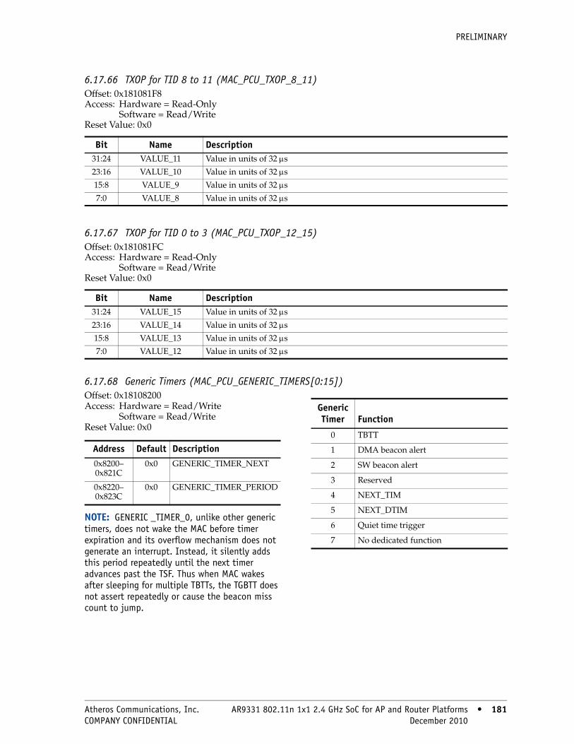
PRELIMINARY
6.17.66 TXOP for TID 8 to 11 (MAC_PCU_TXOP_8_11)Offset: 0x181081F8Access: Hardware = Read-Only
Software = Read/WriteReset Value: 0x0
6.17.67 TXOP for TID 0 to 3 (MAC_PCU_TXOP_12_15)Offset: 0x181081FCAccess: Hardware = Read-Only
Software = Read/WriteReset Value: 0x0
6.17.68 Generic Timers (MAC_PCU_GENERIC_TIMERS[0:15])Offset: 0x18108200Access: Hardware = Read/Write
Software = Read/WriteReset Value: 0x0
NOTE: GENERIC _TIMER_0, unlike other generic timers, does not wake the MAC before timer expiration and its overflow mechanism does not generate an interrupt. Instead, it silently adds this period repeatedly until the next timer advances past the TSF. Thus when MAC wakes after sleeping for multiple TBTTs, the TGBTT does not assert repeatedly or cause the beacon miss count to jump.
Bit Name Description31:24 VALUE_11 Value in units of 32 μs
23:16 VALUE_10 Value in units of 32 μs
15:8 VALUE_9 Value in units of 32 μs
7:0 VALUE_8 Value in units of 32 μs
Bit Name Description31:24 VALUE_15 Value in units of 32 μs
23:16 VALUE_14 Value in units of 32 μs
15:8 VALUE_13 Value in units of 32 μs
7:0 VALUE_12 Value in units of 32 μs
Address Default Description0x8200–0x821C
0x0 GENERIC_TIMER_NEXT
0x8220–0x823C
0x0 GENERIC_TIMER_PERIOD
Generic Timer Function
0 TBTT
1 DMA beacon alert
2 SW beacon alert
3 Reserved
4 NEXT_TIM
5 NEXT_DTIM
6 Quiet time trigger
7 No dedicated function
Atheros Communications, Inc. AR9331 802.11n 1x1 2.4 GHz SoC for AP and Router Platforms • 181 COMPANY CONFIDENTIAL December 2010 • 181
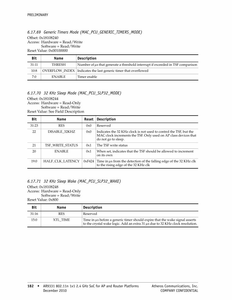
PRELIMINARY
6.17.69 Generic Timers Mode (MAC_PCU_GENERIC_TIMERS_MODE)Offset: 0x18108240Access: Hardware = Read/Write
Software = Read/WriteReset Value: 0x00100000
6.17.70 32 KHz Sleep Mode (MAC_PCU_SLP32_MODE)Offset: 0x18108244Access: Hardware = Read-Only
Software = Read/WriteReset Value: See Field Description
6.17.71 32 KHz Sleep Wake (MAC_PCU_SLP32_WAKE)Offset: 0x18108248Access: Hardware = Read-Only
Software = Read/WriteReset Value: 0x800
Bit Name Description
31:11 THRESH Number of μs that generate a threshold interrupt if exceeded in TSF comparison
10:8 OVERFLOW_INDEX Indicates the last generic timer that overflowed
7:0 ENABLE Timer enable
Bit Name Reset Description
31:23 RES 0x0 Reserved
22 DISABLE_32KHZ 0x0 Indicates the 32 KHz clock is not used to control the TSF, but the MAC clock increments the TSF. Only used on AP class devices that do not go to sleep.
21 TSF_WRITE_STATUS 0x1 The TSF write status
20 ENABLE 0x1 When set, indicates that the TSF should be allowed to increment on its own
19:0 HALF_CLK_LATENCY 0xF424 Time in μs from the detection of the falling edge of the 32 KHz clk to the rising edge of the 32 KHz clk
Bit Name Description
31:16 RES Reserved
15:0 XTL_TIME Time in μs before a generic timer should expire that the wake signal asserts to the crystal wake logic. Add an extra 31 μs due to 32 KHz clock resolution.
182 • AR9331 802.11n 1x1 2.4 GHz SoC for AP and Router Platforms Atheros Communications, Inc. 182 • December 2010 COMPANY CONFIDENTIAL

PRELIMINARY
6.17.72 32 KHz Sleep Increment (MAC_PCU_SLP32_INC)Offset: 0x1810824CAccess: Hardware = Read-Only
Software = Read/WriteReset Value: 0x1E848
6.17.73 Sleep MIB Sleep Count (MAC_PCU_SLP_MIB1)Offset: 0x18108250Access: Hardware = Read/Write
Software = Read/WriteReset Value: 0x0
6.17.74 Sleep MIB Cycle Count (MAC_PCU_SLP_MIB2)Offset: 0x18108254 Access:Hardware = Read/Write
Software = Read/WriteReset Value: 0x0
6.17.75 Sleep MIB Control Status (MAC_PCU_SLP_MIB3)Offset: 0x18108258Access: Hardware = Read/Write
Software = Read/WriteReset Value: 0x0
Bit Name Description
31:20 RES Reserved
19:0 TSF_INC Time in 1/212 of a μs the TSF increments on the rising edge of the 32 KHz clk (30.5176 μs period). The upper 8 bits are at μs resolution. The lower 12 bits are the fractional portion. 1 unit X ________ = __________1/212 ms 30.5176 ms
Where X = 125000, or 0x1E848 is the default setting for 32.768 MHz clock.
Bit Name Description
31:0 SLEEP_CNT Counts the number of 32 KHz clock cycles that the MAC has been asleep
Bit Name Description
31:0 CYCLE_CNT Counts the absolute number of 32KHz clock cycles. When CYCLE_CNT bit 31 is 1, the MIB interrupt will be asserted. SLEEP_CNT and CYCLE_CNT are saturating counters when the value of CYCLE_CNT reaches 0xFFFF_FFFF both counters will stop incrementing.
Bit Name Description
31:2 RES Reserved
1 PENDING SLEEP_CNT, CYCLE_CNT, and CLR_CNT are writable for diagnostic purposes. Before every read/write, the pending bit should be polled to verify any pending write has cleared.
0 CLR_CNT CLR_CNT clears both SLEEP_CNT and CYCLE_CNT. Pending is asserted while the clearing of these registers is pending.
Atheros Communications, Inc. AR9331 802.11n 1x1 2.4 GHz SoC for AP and Router Platforms • 183 COMPANY CONFIDENTIAL December 2010 • 183
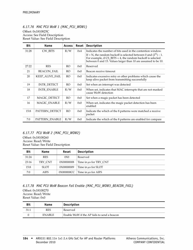
PRELIMINARY
6.17.76 MAC PCU WoW 1 (MAC_PCU_WOW1)Offset: 0x1810825C Access: See Field Description Reset Value: See Field Description
6.17.77 PCU WoW 2 (MAC_PCU_WOW2)Offset: 0x18108260 Access: Read/Write Reset Value: See Field Description
6.17.78 MAC PCU WoW Beacon Fail Enable (MAC_PCU_WOW3_BEACON_FAIL)Offset: 0x18108270 Access: Read/Write Reset Value: 0x0
Bit Name Access Reset Description
31:28 CW_BITS R/W 0x4 Indicates the number of bits used in the contention window. If = N, the random backoff is selected between 0 and (2N) – 1. For example, if CS_BITS = 4, the random backoff is selected between 0 and 15. Values larger than 10 are assumed to be 10.
27:22 RES RO 0x0 Reserved
21 BEACON_FAIL RO 0x0 Beacon receive timeout
20 KEEP_ALIVE_FAIL RO 0x0 Indicates excessive retry or other problems which cause the keep alive packet from transmitting successfully
19 INTR_DETECT RO 0x0 Set when an interrupt was detected
18 INTR_ENABLE R/W 0x0 When set, indicates that MAC interrupts that are not masked cause WoW detection
17 MAGIC_DETECT RO 0x0 Set when a magic packet has been detected
16 MAGIC_ENABLE R/W 0x0 When set, indicates the magic packet detection has been enabled
15:8 PATTERN_DETECT RO 0x0 Indicate the which of the 8 patterns were matched a receive packet
7:0 PATTERN_ENABLE R/W 0x0 Indicate the which of the 8 patterns are enabled for compare
Bit Name Reset Description
31:24 RES 0X0 Reserved
23:16 TRY_CNT 0X00000008 Time in μs for TRY_CNT
15:8 SLOT 0X00000009 Time in μs for SLOT
7:0 AIFS 0X000000CC Time in μs for AIFS
Bit Name Description
31:1 RES Reserved
0 ENABLE Enable WoW if the AP fails to send a beacon
184 • AR9331 802.11n 1x1 2.4 GHz SoC for AP and Router Platforms Atheros Communications, Inc. 184 • December 2010 COMPANY CONFIDENTIAL

PRELIMINARY
6.17.79 MAC PCU WoW Beacon Fail Timeout (MAC_PCU_WOW3_BEACON)Offset: 0x18108274 Access: Read/Write Reset Value: 0x40000000
6.17.80 MAC PCU WoW Keep Alive Timeout (MAC_PCU_WOW3_KEEP_ALIVE)Offset: 0x18108278 Access: Read/Write Reset Value: 0x3E4180
6.17.81 MAC PCU WoW Automatic Keep Alive Disable (MAC_PCU_WOW_KA)Offset: 0x1810827C Access: Read/Write Reset Value: See Field Description
6.17.82 Exact Length and Offset Requirement Flag for WoW Patterns (WOW_EXACT)Offset: 0x1810828C Access: Read/Write Reset Value: See Field Descriptions
Bit Name Description
31:0 TIMEOUT WoW beacon fail timeout value (REFCLK cycles)
Bit Name Description
31:0 TIMEOUT WoW keep alive timeout value (REFCLK cycles)
Bit Name Reset Description
31:3 RES 0x0 Reserved
2 BKOFF_CS_ENABLE
0x00000001 Enable carrier sense during KEEPALIVEBACKOFF state
1 FAIL_DISABLE 0x00000000 Disable WoW If there is a failure in sending keep-alive frames
0 AUTO_DISABLE 0x00000000 Disable automatic transmission of keep-alive frames
Bit Name Reset Description
31:16 RES 0x0 Reserved
15:8 OFFSET 0x00 Exact offset requirement flag for WoW patterns, 1 bit for each pattern
7:0 LENGTH 0xFF Exact length requirement flag for WoW patterns, 1 bit for each pattern
Atheros Communications, Inc. AR9331 802.11n 1x1 2.4 GHz SoC for AP and Router Platforms • 185 COMPANY CONFIDENTIAL December 2010 • 185

PRELIMINARY
6.17.83 WoW Offset 1 (PCU_WOW4)Offset: 0x18108294 Access: Read/Write Reset Value: 0x0
6.17.84 WoW Offset 2 (PCU_WOW5)Offset: 0x18108298 Access: Read/Write Reset Value: 0x0
6.17.85 Global Mode (MAC_PCU_20_40_MODE)Offset: 0x18108318Access: Hardware = Read-Only
Software = Read/WriteReset Value: 0x0
6.17.86 Difference RX_CLEAR Counter (MAC_PCU_RX_CLEAR_DIFF_CNT)Offset: 0x18108328Access: Hardware = Read-Only
Software = Read/WriteReset Value: 0x0
Bit Name Description31:24 OFFSET3 Offset for pattern 3
23:16 OFFSET2 Offset for pattern 2
15:8 OFFSET1 Offset for pattern 1
7:0 OFFSET0 Offset for pattern 0
Bit Name Description31:24 OFFSET7 Offset for pattern 7
23:16 OFFSET6 Offset for pattern 6
15:8 OFFSET5 Offset for pattern 5
7:0 OFFSET4 Offset for pattern 4
Bit Name Description
31:1 RES Reserved
0 JOINED_RX_CLEAR Setting this bit causes the RX_CLEAR used in the MAC to be the AND of the control channel RX_CLEAR and the extension channel RX_CLEAR. If this bit is clear then the MAC will use only the control channel RX_CLEAR.
Bit Name Description
31:0 RX_CLEAR_DIFF_CNT A cycle counter MIB register. On every cycle of the MAC clock, this counter increments every time the extension channel RX_CLEAR is low when the MAC is not actively transmitting or receiving. Due to a small lag between TX_FRAME and RX_CLEAR as well as between RX_CLEAR and RX_FRAME, the count may have some residual value even when no activity is on the extension channel.
186 • AR9331 802.11n 1x1 2.4 GHz SoC for AP and Router Platforms Atheros Communications, Inc. 186 • December 2010 COMPANY CONFIDENTIAL

PRELIMINARY
6.17.87 Control Registers for Block BA Control Fields (MAC_PCU_BA_BAR_CONTROL)Offset: 0x18108330Access: Hardware = Read-Only
Software = Read/WriteReset Value: See Field Description
6.17.88 Legacy PLCP Spoof (MAC_PCU_LEGACY_PLCP_SPOOF)Offset: 0x18108334Access: Hardware = Read-Only
Software = Read/WriteReset Value: See Field Description
6.17.89 PHY Error Mask and EIFS Mask (MAC_PCU_PHY_ERROR_MASK_CONT)Offset: 0x18108338Access: Hardware = Read-Only
Software = Read/WriteReset Value: 0x0
Bit Name Reset Description
31:13 RES 0x0 Reserved
12 UPDATE_BA_BITMAP_QOS_NULL
0x0 When set, it enables the update of BA_BITMAP on a QoS Null frame
11 TX_BA_CLEAR_BA_VALID
0x0 When set, enables the BA_VALID bits to be cleared upon transmit of the block ACK for an aggregate frame or on receiving a BAR
10 FORCE_NO_MATCH 0x0 Causes the BA logic to never find a match of previous saved bitmap in the memory
9 ACK_POLICY_VALUE 0x1 The value of the ACK policy bit
8 COMPRESSED_VALUE 0x1 The value of the compressed bit
7:4 ACK_POLICY_OFFSET 0x0 Indicates the bit offset in the block ACK or block ACK request control field which defines the location of the ACK policy bit.
3:0 COMPRESSED_OFFSET 0x2 Indicates the bit offset in the block ACK or block ACK request control field which defines the location of the COMPRESSED bit.
Bit Name Reset Description
31:9 RES 0X0 Reserved
12:8 MIN_LENGTH 0xE Defines the minimum spoofed legacy PLCP length
7:0 EIFS_MINUS_DIFS
0x0 Defines the number of μs to be subtracted from the transmit packet duration to provide fairness for legacy devices as well as HT devices.
Bit Name Description
31:19 RES Reserved
23:16 EIFS_VALUE Continuation of MAC_PCU_PHY_ERROR_MASK_VALUE. Bits [2], [1], and [0] correspond to PHY errors 34, 33, and 32. All PHY errors above 39 cause EIFS delay.
15:8 RES Reserved
7:0 MASK_VALUE Continuation of MAC_PCU_PHY_ERROR_MASK_VALUE. Bits [2], [1], and [0] correspond to PHY errors 34, 33, and 32. All PHY errors above 39 are filtered.
Atheros Communications, Inc. AR9331 802.11n 1x1 2.4 GHz SoC for AP and Router Platforms • 187 COMPANY CONFIDENTIAL December 2010 • 187

PRELIMINARY
6.17.90 Tx Timer (MAC_PCU_TX_TIMER)Offset: 0x1810833C Access:Hardware = Read/Write Software = Read/Write Reset Value: 0x0
6.17.91 MAC PCU WoW 6 (MAC_PCU_WOW6)Offset: 0x1810834C Access: Read-Only Reset Value: 0x0
6.17.92 MAC PCU WoW 5 (MAC_PCU_WOW5)Offset: 0x1810835C Access: Read/Write Reset Value: 0x0
6.17.93 Length of Pattern Match for Pattern 0 (MAC_PCU_WOW_LENGTH1)Offset: 0x18108360 Access: Read/Write Reset Value: 0xFF
The antenna mask normally comes from the Tx descriptor. For self generated frames, this register provides the antenna mask to the baseband via the MAC/baseband interface.
Bit Name Description
31:16 RES Reserved
15 TX_TIMER_ENABLE Enabled when this bit is set to 1
14:0 TX_TIMER Guarantees the transmit frame does not take more time than the values programmed in this timer. The unit for this timer is in μs.
Bit Name Description
31:16 RES Reserved
15:0 RXBUF_START_ADDR Indicates the start address of the frame in RxBUF that caused the WoW event
Bit Name Description
31:16 RES Reserved
15:0 RX_ABORT_ENABLE Enables generation of RX_ABORT when a pattern is matched
Bit Name Description
31:24 PATTERN_0 Used for pattern matching length of the WoW feature
23:16 PATTERN_1 Used for pattern matching length of the WoW feature
15:8 PATTERN_2 Used for pattern matching length of the WoW feature
7:0 PATTERN_3 Used for pattern matching length of the WoW feature
188 • AR9331 802.11n 1x1 2.4 GHz SoC for AP and Router Platforms Atheros Communications, Inc. 188 • December 2010 COMPANY CONFIDENTIAL
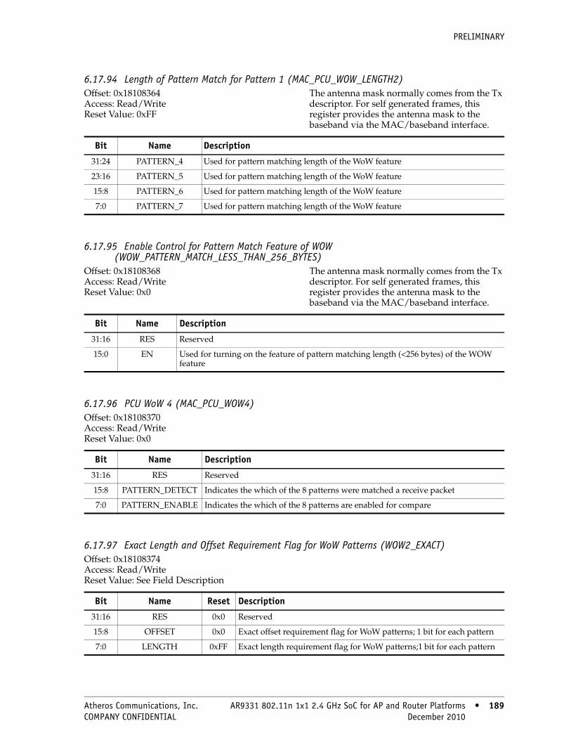
PRELIMINARY
6.17.94 Length of Pattern Match for Pattern 1 (MAC_PCU_WOW_LENGTH2)Offset: 0x18108364 Access: Read/Write Reset Value: 0xFF
The antenna mask normally comes from the Tx descriptor. For self generated frames, this register provides the antenna mask to the baseband via the MAC/baseband interface.
6.17.95 Enable Control for Pattern Match Feature of WOW (WOW_PATTERN_MATCH_LESS_THAN_256_BYTES)
Offset: 0x18108368 Access: Read/Write Reset Value: 0x0
The antenna mask normally comes from the Tx descriptor. For self generated frames, this register provides the antenna mask to the baseband via the MAC/baseband interface.
6.17.96 PCU WoW 4 (MAC_PCU_WOW4)Offset: 0x18108370 Access: Read/Write Reset Value: 0x0
6.17.97 Exact Length and Offset Requirement Flag for WoW Patterns (WOW2_EXACT)Offset: 0x18108374 Access: Read/Write Reset Value: See Field Description
Bit Name Description
31:24 PATTERN_4 Used for pattern matching length of the WoW feature
23:16 PATTERN_5 Used for pattern matching length of the WoW feature
15:8 PATTERN_6 Used for pattern matching length of the WoW feature
7:0 PATTERN_7 Used for pattern matching length of the WoW feature
Bit Name Description
31:16 RES Reserved
15:0 EN Used for turning on the feature of pattern matching length (<256 bytes) of the WOW feature
Bit Name Description
31:16 RES Reserved
15:8 PATTERN_DETECT Indicates the which of the 8 patterns were matched a receive packet
7:0 PATTERN_ENABLE Indicates the which of the 8 patterns are enabled for compare
Bit Name Reset Description
31:16 RES 0x0 Reserved
15:8 OFFSET 0x0 Exact offset requirement flag for WoW patterns; 1 bit for each pattern
7:0 LENGTH 0xFF Exact length requirement flag for WoW patterns;1 bit for each pattern
Atheros Communications, Inc. AR9331 802.11n 1x1 2.4 GHz SoC for AP and Router Platforms • 189 COMPANY CONFIDENTIAL December 2010 • 189
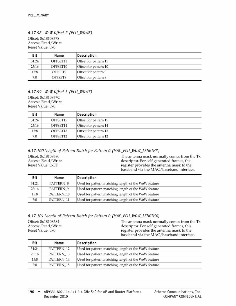
PRELIMINARY
6.17.98 WoW Offset 2 (PCU_WOW6)Offset: 0x18108378 Access: Read/Write Reset Value: 0x0
6.17.99 WoW Offset 3 (PCU_WOW7)Offset: 0x1810837C Access: Read/Write Reset Value: 0x0
6.17.100 Length of Pattern Match for Pattern 0 (MAC_PCU_WOW_LENGTH3)Offset: 0x18108380 Access: Read/Write Reset Value: 0xFF
The antenna mask normally comes from the Tx descriptor. For self generated frames, this register provides the antenna mask to the baseband via the MAC/baseband interface.
6.17.101 Length of Pattern Match for Pattern 0 (MAC_PCU_WOW_LENGTH4)Offset: 0x18108384 Access: Read/Write Reset Value: 0x0
The antenna mask normally comes from the Tx descriptor. For self generated frames, this register provides the antenna mask to the baseband via the MAC/baseband interface.
Bit Name Description31:24 OFFSET11 Offset for pattern 11
23:16 OFFSET10 Offset for pattern 10
15:8 OFFSET9 Offset for pattern 9
7:0 OFFSET8 Offset for pattern 8
Bit Name Description31:24 OFFSET15 Offset for pattern 15
23:16 OFFSET14 Offset for pattern 14
15:8 OFFSET13 Offset for pattern 13
7:0 OFFSET12 Offset for pattern 12
Bit Name Description31:24 PATTERN_8 Used for pattern matching length of the WoW feature
23:16 PATTERN_9 Used for pattern matching length of the WoW feature
15:8 PATTERN_10 Used for pattern matching length of the WoW feature
7:0 PATTERN_11 Used for pattern matching length of the WoW feature
Bit Name Description31:24 PATTERN_12 Used for pattern matching length of the WoW feature
23:16 PATTERN_13 Used for pattern matching length of the WoW feature
15:8 PATTERN_14 Used for pattern matching length of the WoW feature
7:0 PATTERN_15 Used for pattern matching length of the WoW feature
190 • AR9331 802.11n 1x1 2.4 GHz SoC for AP and Router Platforms Atheros Communications, Inc. 190 • December 2010 COMPANY CONFIDENTIAL

PRELIMINARY
6.17.102 TID Value Access Category (MAC_PCU_TID_TO_AC)Offset: 0x181083A4 Access: Read/Write Reset Value: 0x0
6.17.103 High Priority Queue Control (MAC_PCU_HP_QUEUE)Offset: 0x181083A8 Access: Read/Write Reset Value: See Field Descriptions
Bit Name Description
31:0 DATA Maps the 16 user priority TID values to corresponding access category (AC). Two bits denote the AC for each TID. Bits [1:0] define the AC for TID 0 and next two bits are used for AC of TID 1, and finally bits [31:30] define the AC for TID 15. Default values are as specified in the 11e specification: TID 1 and 2 are BK, TID 0 and 3 are BK, TID 4 and 5 are VI, and TID 6 and 7 are V0. ACs:
00 BE
01 BK
10 VI
11 VO
Bit Name Reset Description
31:21 RES 0x0 Reserved
20 UAPSD_EN 0xF Enable UAPSD trigger
19:16 FRAME_SUBTYPE_MASK0 0x0 Frame subtype mask for FRAME_SUBTYPE0, to be matched for the frame to be placed in high priority receive queue
15:12 FRAME_SUBTYPE0 0x0 Frame sub type to be matched for the frame to be placed in high priority receive queue
11:10 FRAME_TYPE_MASK0 0x3 Frame type mask for FRAME_TYPE0, to be matched for the frame to be placed in high priority receive queue
9:8 FRAME_TYPE0 0x0 Frame type to be matched for the frame to be placed in high priority receive queue
7 FRAME_BSSID_MATCH0 0x0 If set to 1, frames with matching BSSID are only moved to high priority receive queue on a frame type match
6 FRAME_FILTER_ENABLE0 0x0 Enables the mode where a frame is moved to high priority receive queue based on frame type
5 HPQON_UAPSD 0x0 Set to 1 if UAPSD receive frame needs to be placed in high priority receive queue. If UAPSD is enable is set for AC of an error free QoS frame with Address1 match with AP address, the frame will be placed in high priority receive queue
4 AC_MASK_VO 0x0 Set to 1 if BK traffic needs to be placed in high priority Rx queue
3 AC_MASK_VI 0x0 Set to 1 if VI traffic needs to be placed in high priority Rx queue
2 AC_MASK_BK 0x0 Set to 1 if BK traffic needs to be placed in high priority Rx queue
1 AC_MASK_BE 0x0 Set to 1 if BE traffic needs to be placed in high priority Rx queue
0 ENABLE 0x0 Enables high priority Rx queue
Atheros Communications, Inc. AR9331 802.11n 1x1 2.4 GHz SoC for AP and Router Platforms • 191 COMPANY CONFIDENTIAL December 2010 • 191
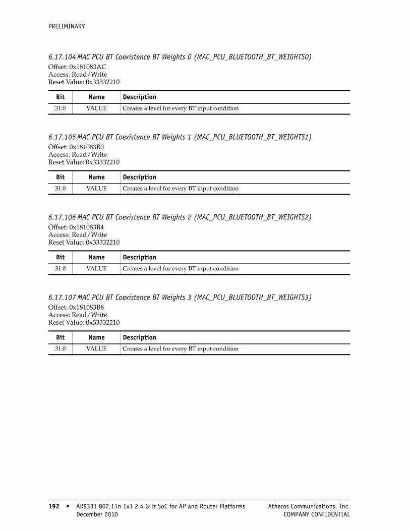
PRELIMINARY
6.17.104 MAC PCU BT Coexistence BT Weights 0 (MAC_PCU_BLUETOOTH_BT_WEIGHTS0)Offset: 0x181083AC Access: Read/Write Reset Value: 0x33332210
6.17.105 MAC PCU BT Coexistence BT Weights 1 (MAC_PCU_BLUETOOTH_BT_WEIGHTS1)Offset: 0x181083B0 Access: Read/Write Reset Value: 0x33332210
6.17.106 MAC PCU BT Coexistence BT Weights 2 (MAC_PCU_BLUETOOTH_BT_WEIGHTS2)Offset: 0x181083B4 Access: Read/Write Reset Value: 0x33332210
6.17.107 MAC PCU BT Coexistence BT Weights 3 (MAC_PCU_BLUETOOTH_BT_WEIGHTS3)Offset: 0x181083B8 Access: Read/Write Reset Value: 0x33332210
Bit Name Description
31:0 VALUE Creates a level for every BT input condition
Bit Name Description
31:0 VALUE Creates a level for every BT input condition
Bit Name Description
31:0 VALUE Creates a level for every BT input condition
Bit Name Description
31:0 VALUE Creates a level for every BT input condition
192 • AR9331 802.11n 1x1 2.4 GHz SoC for AP and Router Platforms Atheros Communications, Inc. 192 • December 2010 COMPANY CONFIDENTIAL
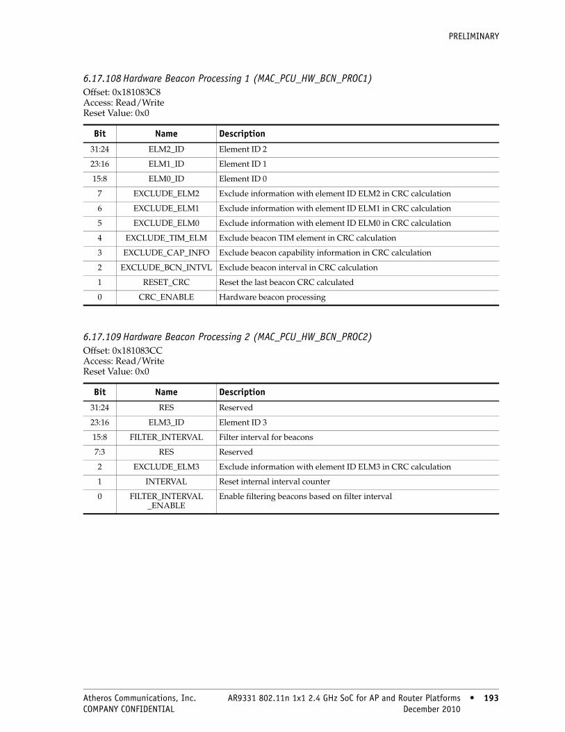
PRELIMINARY
6.17.108 Hardware Beacon Processing 1 (MAC_PCU_HW_BCN_PROC1)Offset: 0x181083C8 Access: Read/Write Reset Value: 0x0
6.17.109 Hardware Beacon Processing 2 (MAC_PCU_HW_BCN_PROC2)Offset: 0x181083CC Access: Read/Write Reset Value: 0x0
Bit Name Description
31:24 ELM2_ID Element ID 2
23:16 ELM1_ID Element ID 1
15:8 ELM0_ID Element ID 0
7 EXCLUDE_ELM2 Exclude information with element ID ELM2 in CRC calculation
6 EXCLUDE_ELM1 Exclude information with element ID ELM1 in CRC calculation
5 EXCLUDE_ELM0 Exclude information with element ID ELM0 in CRC calculation
4 EXCLUDE_TIM_ELM Exclude beacon TIM element in CRC calculation
3 EXCLUDE_CAP_INFO Exclude beacon capability information in CRC calculation
2 EXCLUDE_BCN_INTVL Exclude beacon interval in CRC calculation
1 RESET_CRC Reset the last beacon CRC calculated
0 CRC_ENABLE Hardware beacon processing
Bit Name Description
31:24 RES Reserved
23:16 ELM3_ID Element ID 3
15:8 FILTER_INTERVAL Filter interval for beacons
7:3 RES Reserved
2 EXCLUDE_ELM3 Exclude information with element ID ELM3 in CRC calculation
1 INTERVAL Reset internal interval counter
0 FILTER_INTERVAL_ENABLE
Enable filtering beacons based on filter interval
Atheros Communications, Inc. AR9331 802.11n 1x1 2.4 GHz SoC for AP and Router Platforms • 193 COMPANY CONFIDENTIAL December 2010 • 193
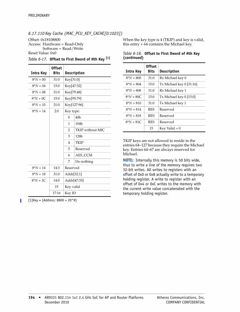
PRELIMINARY
6.17.110 Key Cache (MAC_PCU_KEY_CACHE[0:1023])Offset: 0x18108800Access: Hardware = Read-Only
Software = Read/WriteReset Value: 0x0
When the key type is 4 (TKIP) and key is valid, this entry + 64 contains the Michael key.
TKIP keys are not allowed to reside in the entries 64–127 because they require the Michael key. Entries 64–67 are always reserved for Michael.
NOTE: Internally this memory is 50 bits wide, thus to write a line of the memory requires two 32-bit writes. All writes to registers with an offset of 0x0 or 0x8 actually write to a temporary holding register. A write to register with an offset of 0x4 or 0xC writes to the memory with the current write value concatenated with the temporary holding register.
Table 6-17. Offset to First Dword of Nth Key [1]
[1]Key = (Address: 8800 + 20*N)
Intra KeyOffset Bits Description
8*N + 00 31:0 Key[31:0]
8*N + 04 15:0 Key[47:32]
8*N + 08 31:0 Key[79:48]
8*N + 0C 15:0 Key[95:79]
8*N + 10 31:0 Key[127:96]
8*N + 14 2:0 Key type:
0 40b
1 104b
2 TKIP without MIC
3 128b
4 TKIP
5 Reserved
6 AES_CCM
7 Do nothing
8*N + 14 14:3 Reserved
8*N + 18 31:0 Addr[32:1]
8*N + 1C 14:0 Addr[47:33]
15 Key valid
17:16 Key ID
Table 6-18. Offset to First Dword of Nth Key (continued)
Intra KeyOffset Bits Description
8*N + 800 31:0 Rx Michael key 0
8*N + 804 15:0 Tx Michael key 0 [31:16]
8*N + 808 31:0 Rx Michael key 1
8*N + 80C 15:0 Tx Michael key 0 [15:0]
8*N + 810 31:0 Tx Michael key 1
8*N + 814 RES Reserved
8*N + 818 RES Reserved
8*N + 81C RES Reserved
15 Key Valid = 0
194 • AR9331 802.11n 1x1 2.4 GHz SoC for AP and Router Platforms Atheros Communications, Inc. 194 • December 2010 COMPANY CONFIDENTIAL

PRELIMINARY
6.18 Ethernet RegistersTable 6-19 summarizes the Ethernet registers for the AR9331.
Table 6-19. Ethernet Registers Summary
GE0 Address GE1 Address Description Page
0x19000000 0x1A000000 MAC Configuration 1 page 198
0x19000004 0x1A000004 MAC Configuration 2 page 199
0x19000008 0x1A000008 IPG/IFG page 200
0x1900000C 0x1A00000C Half-Duplex page 200
0x19000010 0x1A000010 Maximum Frame Length page 201
0x19000020 0x1A100020 MII Configuration page 201
0x19000024 0x1A000024 MII Command page 202
0x19000028 0x1A000028 MII Address page 202
0x1900002C 0x1A00002C MII Control page 203
0x19000030 0x1A000030 MII Status page 203
0x19000034 0x1A000034 MII Indicators page 203
0x19000038 0x1A000038 Interface Control page 203
0x1900003C 0x1A00003C Interface Status page 204
0x19000040 0x1A000040 STA Address 1 page 205
0x19000044 0x1A000044 STA Address 2 page 206
0x19000048 0x1A000048 ETH Configuration 0 page 206
0x1900004C 0x1A00004C ETH Configuration 1 page 206
0x19000050 0x1A000050 ETH Configuration 2 page 207
0x19000054 0x1A000054 ETH Configuration 3 page 207
0x19000058 0x1A000058 ETH Configuration 4 page 208
0x1900005C 0x1A00005C ETH Configuration 5 page 209
0x19000080 0x1A000080 TR64 Tx/Rx 64 Byte Frame Counter page 209
0x19000084 0x1A000084 TR127 Tx/Rx 65-127 Byte Frame Counter page 209
0x19000088 0x1A000088 TR255 Tx/Rx 128-255 Byte Frame Counter page 209
0x1900008C 0x1A00008C TR511 Tx/Rx 256-511 Byte Frame Counter page 210
0x19000090 0x1A000090 TR1K Tx/Rx 512-1023 Byte Frame Counter page 210
0x19000094 0x1A000094 TRMAX Tx/Rx 1024-1518 Byte Frame Counter page 210
0x19000098 0x1A000098 TRMGV Tx/Rx 1519-1522 Byte VLAN Frame Counter page 210
0x1900009C 0x1A00009C RBYT Receive Byte Counter page 211
0x190000A0 0x1A0000A0 RPKT Receive Packet Counter page 211
0x190000A4 0x1A0000A4 RFCS Receive FCS Error Counter page 211
0x190000A8 0x1A0000A8 RMCA Receive Multicast Packet Counter page 211
0x190000AC 0x1A0000AC RBCA Receive Broadcast Packet Counter page 212
0x190000B0 0x1A0000B0 RXCF Receive Control Frame Packet Counter page 212
Atheros Communications, Inc. AR9331 802.11n 1x1 2.4 GHz SoC for AP and Router Platforms • 195 COMPANY CONFIDENTIAL December 2010 • 195
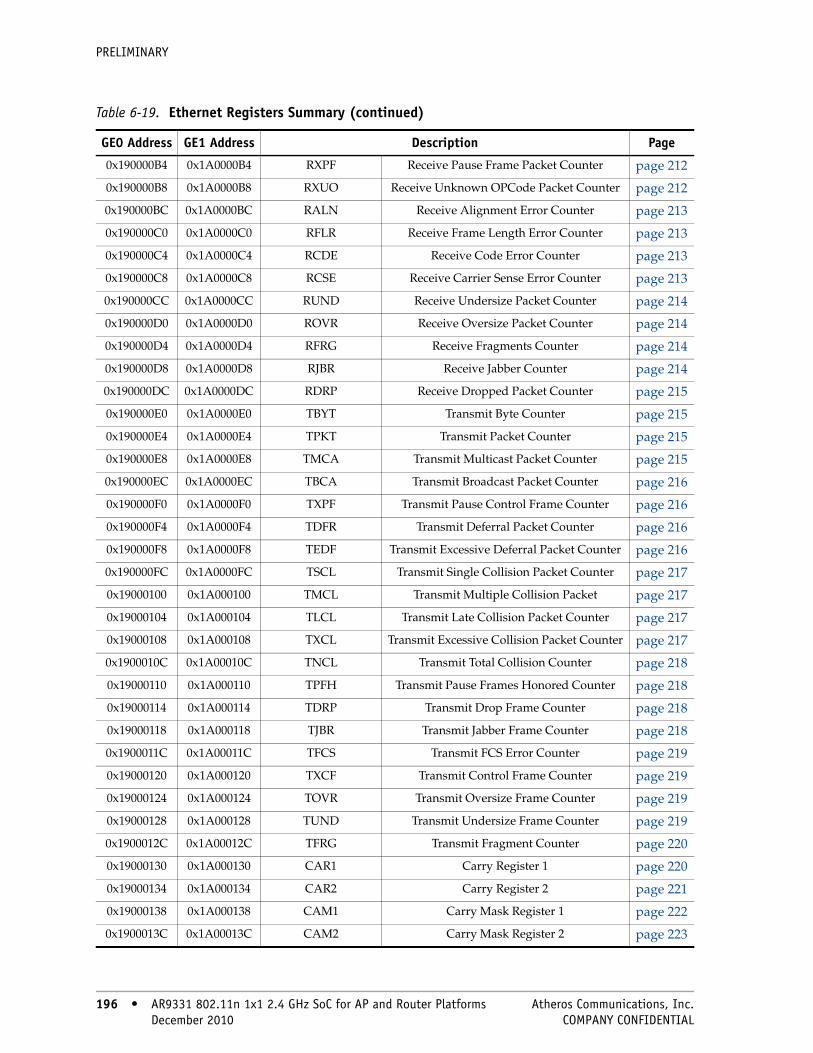
PRELIMINARY
0x190000B4 0x1A0000B4 RXPF Receive Pause Frame Packet Counter page 212
0x190000B8 0x1A0000B8 RXUO Receive Unknown OPCode Packet Counter page 212
0x190000BC 0x1A0000BC RALN Receive Alignment Error Counter page 213
0x190000C0 0x1A0000C0 RFLR Receive Frame Length Error Counter page 213
0x190000C4 0x1A0000C4 RCDE Receive Code Error Counter page 213
0x190000C8 0x1A0000C8 RCSE Receive Carrier Sense Error Counter page 213
0x190000CC 0x1A0000CC RUND Receive Undersize Packet Counter page 214
0x190000D0 0x1A0000D0 ROVR Receive Oversize Packet Counter page 214
0x190000D4 0x1A0000D4 RFRG Receive Fragments Counter page 214
0x190000D8 0x1A0000D8 RJBR Receive Jabber Counter page 214
0x190000DC 0x1A0000DC RDRP Receive Dropped Packet Counter page 215
0x190000E0 0x1A0000E0 TBYT Transmit Byte Counter page 215
0x190000E4 0x1A0000E4 TPKT Transmit Packet Counter page 215
0x190000E8 0x1A0000E8 TMCA Transmit Multicast Packet Counter page 215
0x190000EC 0x1A0000EC TBCA Transmit Broadcast Packet Counter page 216
0x190000F0 0x1A0000F0 TXPF Transmit Pause Control Frame Counter page 216
0x190000F4 0x1A0000F4 TDFR Transmit Deferral Packet Counter page 216
0x190000F8 0x1A0000F8 TEDF Transmit Excessive Deferral Packet Counter page 216
0x190000FC 0x1A0000FC TSCL Transmit Single Collision Packet Counter page 217
0x19000100 0x1A000100 TMCL Transmit Multiple Collision Packet page 217
0x19000104 0x1A000104 TLCL Transmit Late Collision Packet Counter page 217
0x19000108 0x1A000108 TXCL Transmit Excessive Collision Packet Counter page 217
0x1900010C 0x1A00010C TNCL Transmit Total Collision Counter page 218
0x19000110 0x1A000110 TPFH Transmit Pause Frames Honored Counter page 218
0x19000114 0x1A000114 TDRP Transmit Drop Frame Counter page 218
0x19000118 0x1A000118 TJBR Transmit Jabber Frame Counter page 218
0x1900011C 0x1A00011C TFCS Transmit FCS Error Counter page 219
0x19000120 0x1A000120 TXCF Transmit Control Frame Counter page 219
0x19000124 0x1A000124 TOVR Transmit Oversize Frame Counter page 219
0x19000128 0x1A000128 TUND Transmit Undersize Frame Counter page 219
0x1900012C 0x1A00012C TFRG Transmit Fragment Counter page 220
0x19000130 0x1A000130 CAR1 Carry Register 1 page 220
0x19000134 0x1A000134 CAR2 Carry Register 2 page 221
0x19000138 0x1A000138 CAM1 Carry Mask Register 1 page 222
0x1900013C 0x1A00013C CAM2 Carry Mask Register 2 page 223
Table 6-19. Ethernet Registers Summary (continued)
GE0 Address GE1 Address Description Page
196 • AR9331 802.11n 1x1 2.4 GHz SoC for AP and Router Platforms Atheros Communications, Inc. 196 • December 2010 COMPANY CONFIDENTIAL
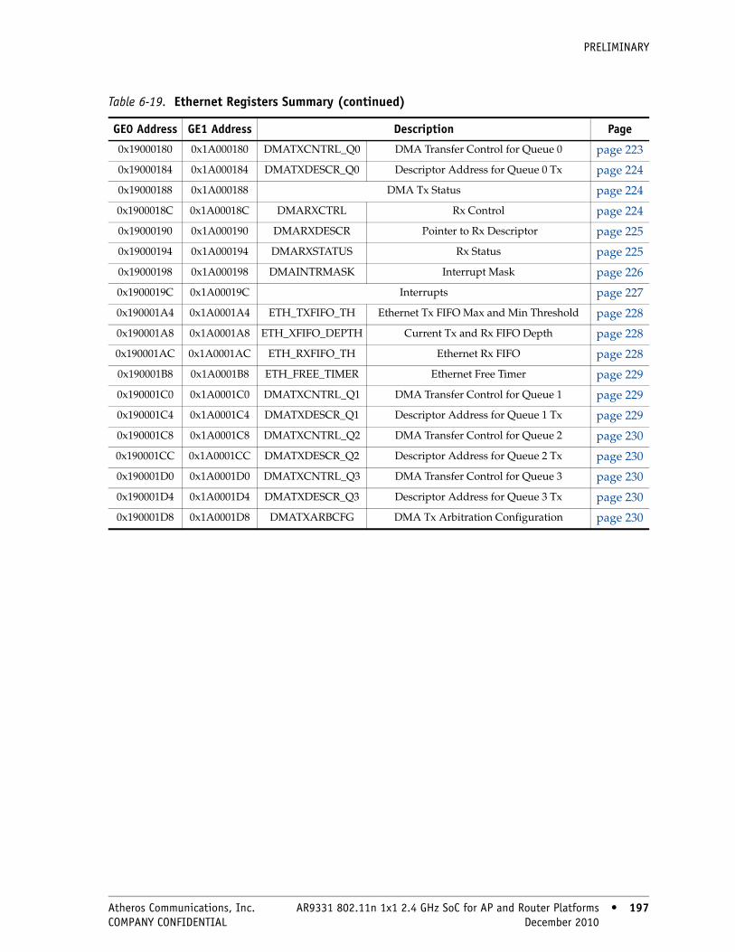
PRELIMINARY
0x19000180 0x1A000180 DMATXCNTRL_Q0 DMA Transfer Control for Queue 0 page 223
0x19000184 0x1A000184 DMATXDESCR_Q0 Descriptor Address for Queue 0 Tx page 224
0x19000188 0x1A000188 DMA Tx Status page 224
0x1900018C 0x1A00018C DMARXCTRL Rx Control page 224
0x19000190 0x1A000190 DMARXDESCR Pointer to Rx Descriptor page 225
0x19000194 0x1A000194 DMARXSTATUS Rx Status page 225
0x19000198 0x1A000198 DMAINTRMASK Interrupt Mask page 226
0x1900019C 0x1A00019C Interrupts page 227
0x190001A4 0x1A0001A4 ETH_TXFIFO_TH Ethernet Tx FIFO Max and Min Threshold page 228
0x190001A8 0x1A0001A8 ETH_XFIFO_DEPTH Current Tx and Rx FIFO Depth page 228
0x190001AC 0x1A0001AC ETH_RXFIFO_TH Ethernet Rx FIFO page 228
0x190001B8 0x1A0001B8 ETH_FREE_TIMER Ethernet Free Timer page 229
0x190001C0 0x1A0001C0 DMATXCNTRL_Q1 DMA Transfer Control for Queue 1 page 229
0x190001C4 0x1A0001C4 DMATXDESCR_Q1 Descriptor Address for Queue 1 Tx page 229
0x190001C8 0x1A0001C8 DMATXCNTRL_Q2 DMA Transfer Control for Queue 2 page 230
0x190001CC 0x1A0001CC DMATXDESCR_Q2 Descriptor Address for Queue 2 Tx page 230
0x190001D0 0x1A0001D0 DMATXCNTRL_Q3 DMA Transfer Control for Queue 3 page 230
0x190001D4 0x1A0001D4 DMATXDESCR_Q3 Descriptor Address for Queue 3 Tx page 230
0x190001D8 0x1A0001D8 DMATXARBCFG DMA Tx Arbitration Configuration page 230
Table 6-19. Ethernet Registers Summary (continued)
GE0 Address GE1 Address Description Page
Atheros Communications, Inc. AR9331 802.11n 1x1 2.4 GHz SoC for AP and Router Platforms • 197 COMPANY CONFIDENTIAL December 2010 • 197
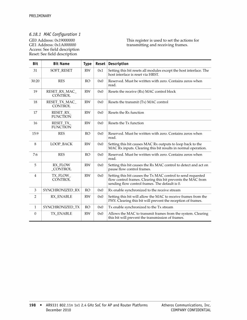
PRELIMINARY
6.18.1 MAC Configuration 1GE0 Address: 0x19000000 GE1 Address: 0x1A000000 Access: See field description Reset: See field description
This register is used to set the actions for transmitting and receiving frames.
Bit Bit Name Type Reset Description
31 SOFT_RESET RW 0x1 Setting this bit resets all modules except the host interface. The host interface is reset via HRST.
30:20 RES RO 0x0 Reserved. Must be written with zero. Contains zeros when read.
19 RESET_RX_MAC_ CONTROL
RW 0x0 Resets the receive (Rx) MAC control block
18 RESET_TX_MAC_ CONTROL
RW 0x0 Resets the transmit (Tx) MAC control
17 RESET_RX_ FUNCTION
RW 0x0 Resets the Rx function
16 RESET_TX_ FUNCTION
RW 0x0 Resets the Tx function
15:9 RES RO 0x0 Reserved. Must be written with zero. Contains zeros when read.
8 LOOP_BACK RW 0x0 Setting this bit causes MAC Rx outputs to loop back to the MAC Rx inputs. Clearing this bit results in normal operation.
7:6 RES RO 0x0 Reserved. Must be written with zero. Contains zeros when read.
5 RX_FLOW_CONTROL
RW 0x0 Setting this bit causes the Rx MAC control to detect and act on pause flow control frames.
4 TX_FLOW_ CONTROL
RW 0x0 Setting this bit causes the Tx MAC control to send requested flow control frames. Clearing this bit prevents the MAC from sending flow control frames. The default is 0.
3 SYNCHRONIZED_RX RO 0x0 Rx enable synchronized to the receive stream
2 RX_ENABLE RW 0x0 Setting this bit will allow the MAC to receive frames from the PHY. Clearing this bit will prevent the reception of frames.
1 SYNCHRONIZED_TX RO 0x0 Tx enable synchronized to the Tx stream
0 TX_ENABLE RW 0x0 Allows the MAC to transmit frames from the system. Clearing this bit will prevent the transmission of frames.
198 • AR9331 802.11n 1x1 2.4 GHz SoC for AP and Router Platforms Atheros Communications, Inc. 198 • December 2010 COMPANY CONFIDENTIAL

PRELIMINARY
6.18.2 MAC Configuration 2GE0 Address: 0x19000004 GE1 Address: 0x1A000004 Access: Read/Write Reset: See field description
This register is used to set the parameters relating to the MAC, including duplex, CRC, and oversized frames.
Bit Bit Name Reset Description31:16 RES 0x0 Reserved. Must be written with zero. Contains zeros when read.
15:12 PREAMBLE_ LENGTH
0x7 Determines the length of the preamble field of the packet, in bytes.
11:10 RES 0x0 Reserved. Must be written with zero. Contains zeros when read.
9:8 INTERFACE_ MODE
0x0 Determines the type of interface to which the MAC is connected.
Interface Mode Bit [9] Bit [8]
RESERVED 0 0
Nibble Mode (10/100 Mbps MII/RMII/SMII...) 0 1
RESERVED 1 0
RESERVED 1 1
7:6 RES 0x0 Reserved. Must be written with zero. Contains zeros when read.
5 HUGE_FRAME 0x0 Set this bit to allow frames longer than the MAXIMUM FRAME LENGTH to be transmitted and received. Clear this bit to have the MAC limit the length of frames at the MAXIMUM FRAME LENGTH value, which is contained in the “Maximum Frame Length” register.
4 LENGTH_FIELD 0x0 Set this bit to cause the MAC to check the frame’s length field to ensure it matches the actual data field length. Clear this bit if no length field checking is desired.
3 RES 0x0 Reserved. Must be written with zero. Contains zeros when read.
2 PAD/CRC ENABLE
0x0 Set this bit to have the MAC pad all short frames and append a CRC to every frame whether or not padding was required. Clear this bit if frames presented to the MAC have a valid length and contain a CRC.
1 CRC_ENABLE 0x0 Set this bit to have the MAC append a CRC to all frames. Clear this bit if frames presented to the MAC have a valid length and contain a valid CRC.
0 FULL_DUPLEX 0x0 Setting this bit configures the MAC to operate in full-duplex mode. Clearing this bit configures the MAC to operate in half-duplex mode only.
Atheros Communications, Inc. AR9331 802.11n 1x1 2.4 GHz SoC for AP and Router Platforms • 199 COMPANY CONFIDENTIAL December 2010 • 199
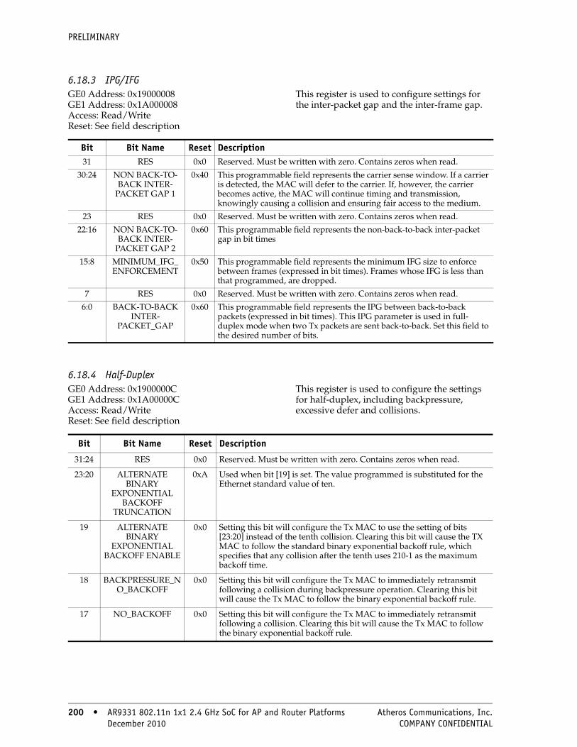
PRELIMINARY
6.18.3 IPG/IFGGE0 Address: 0x19000008 GE1 Address: 0x1A000008 Access: Read/Write Reset: See field description
This register is used to configure settings for the inter-packet gap and the inter-frame gap.
6.18.4 Half-DuplexGE0 Address: 0x1900000C GE1 Address: 0x1A00000C Access: Read/Write Reset: See field description
This register is used to configure the settings for half-duplex, including backpressure, excessive defer and collisions.
Bit Bit Name Reset Description31 RES 0x0 Reserved. Must be written with zero. Contains zeros when read.
30:24 NON BACK-TO-BACK INTER-
PACKET GAP 1
0x40 This programmable field represents the carrier sense window. If a carrier is detected, the MAC will defer to the carrier. If, however, the carrier becomes active, the MAC will continue timing and transmission, knowingly causing a collision and ensuring fair access to the medium.
23 RES 0x0 Reserved. Must be written with zero. Contains zeros when read.
22:16 NON BACK-TO-BACK INTER-
PACKET GAP 2
0x60 This programmable field represents the non-back-to-back inter-packet gap in bit times
15:8 MINIMUM_IFG_ ENFORCEMENT
0x50 This programmable field represents the minimum IFG size to enforce between frames (expressed in bit times). Frames whose IFG is less than that programmed, are dropped.
7 RES 0x0 Reserved. Must be written with zero. Contains zeros when read.
6:0 BACK-TO-BACK INTER-
PACKET_GAP
0x60 This programmable field represents the IPG between back-to-back packets (expressed in bit times). This IPG parameter is used in full- duplex mode when two Tx packets are sent back-to-back. Set this field to the desired number of bits.
Bit Bit Name Reset Description
31:24 RES 0x0 Reserved. Must be written with zero. Contains zeros when read.
23:20 ALTERNATE BINARY
EXPONENTIAL BACKOFF
TRUNCATION
0xA Used when bit [19] is set. The value programmed is substituted for the Ethernet standard value of ten.
19 ALTERNATE BINARY
EXPONENTIAL BACKOFF ENABLE
0x0 Setting this bit will configure the Tx MAC to use the setting of bits [23:20] instead of the tenth collision. Clearing this bit will cause the TX MAC to follow the standard binary exponential backoff rule, which specifies that any collision after the tenth uses 210-1 as the maximum backoff time.
18 BACKPRESSURE_NO_BACKOFF
0x0 Setting this bit will configure the Tx MAC to immediately retransmit following a collision during backpressure operation. Clearing this bit will cause the Tx MAC to follow the binary exponential backoff rule.
17 NO_BACKOFF 0x0 Setting this bit will configure the Tx MAC to immediately retransmit following a collision. Clearing this bit will cause the Tx MAC to follow the binary exponential backoff rule.
200 • AR9331 802.11n 1x1 2.4 GHz SoC for AP and Router Platforms Atheros Communications, Inc. 200 • December 2010 COMPANY CONFIDENTIAL

PRELIMINARY
6.18.5 Maximum Frame LengthGE0 Address: 0x19000010 GE1 Address: 0x1A000010 Access: Read/Write Reset: 0x600
This register is used to set the maximum allowable frame length.
6.18.6 MII ConfigurationGE0 Address: 0x19000020 GE1 Address: 0x1A000020 Access: Read/Write Reset: 0x0
This register is used to set the MII management parameters.
16 EXCESSIVE_ DEFER
0x1 Setting this bit will configure the Tx MAC to allow the transmission of a packet that has been excessively deferred. Clearing this bit will cause the Tx MAC to abort the transmission of a packet that has been excessively deferred.
15:12 RETRANSMISSION_MAXIMUM
0xF This is a programmable field specifying the number of retransmission attempts following a collision before aborting the packet due to excessive collisions. The maximum number of attempts is defined by 802.11 standards as 0xF.
11:10 RES 0x0 Reserved. Must be written with zero. Contains zeros when read.
9:0 COLLISION_ WINDOW
0x37 This programmable field represents the slot time or collision window during which collisions might occur in a properly configured network. Since the collision window starts at the beginning of a transmission, the preamble and SFD are included. The reset value (0x37) corresponds to the count of frame bytes at the end of the window. If the value is larger than 0x3F the TPST single will no longer work correctly.
Bit Bit Name Description
31:16 RES Reserved. Must be written with zero. Contains zeros when read.
15:0 MAX_FRAME_LENGTH
This programmable field sets the maximum frame size in both the Tx and Rx directions
Bit Bit Name Description31 RESET_MII_
MGMTSetting this bit resets the MII Management. Clearing this bit allows MII Management to perform management read/write cycles as requested by the Host interface.
30:6 RES Reserved. Must be written with zero. Contains zeros when read.5 SCAN_AUTO_
INCREMENTSetting this bit causes MII Management to continually read from a set of contiguous PHYs. The starting address of the PHY is specified by the PHY address field recorded in the MII Address register. The next PHY to be read will be PHY address + 1. The last PHY to be queried in this read sequence will be the one residing at address 0x31, after which the read sequence will return to the PHY specified by the PHY address field.
4 PREAMBLE_ SUPRESSION
Setting this bit causes MII Management to suppress preamble generation and reduce the management cycle from 64 clocks to 32 clocks. Clearing this bit causes MII Management to perform Management read/write cycles with the 64 clocks of preamble.
Atheros Communications, Inc. AR9331 802.11n 1x1 2.4 GHz SoC for AP and Router Platforms • 201 COMPANY CONFIDENTIAL December 2010 • 201
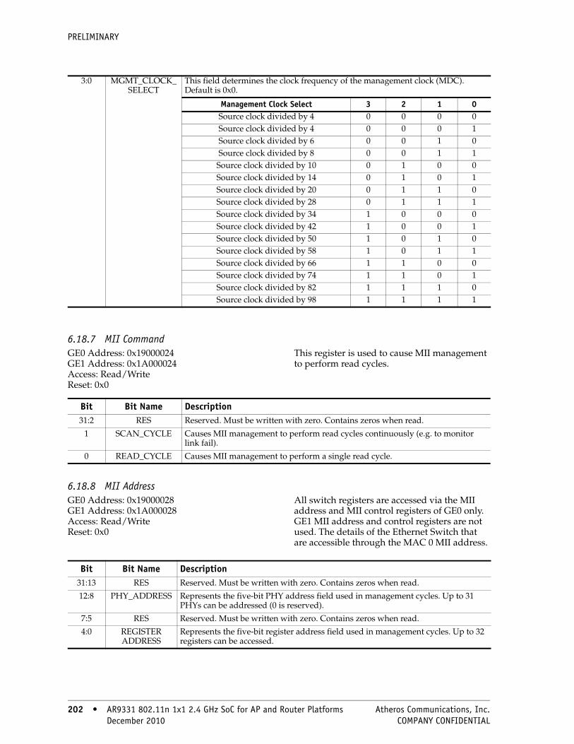
PRELIMINARY
6.18.7 MII CommandGE0 Address: 0x19000024 GE1 Address: 0x1A000024 Access: Read/Write Reset: 0x0
This register is used to cause MII management to perform read cycles.
6.18.8 MII AddressGE0 Address: 0x19000028GE1 Address: 0x1A000028 Access: Read/Write Reset: 0x0
All switch registers are accessed via the MII address and MII control registers of GE0 only. GE1 MII address and control registers are not used. The details of the Ethernet Switch that are accessible through the MAC 0 MII address.
3:0 MGMT_CLOCK_ SELECT
This field determines the clock frequency of the management clock (MDC). Default is 0x0.
Management Clock Select 3 2 1 0Source clock divided by 4 0 0 0 0Source clock divided by 4 0 0 0 1Source clock divided by 6 0 0 1 0Source clock divided by 8 0 0 1 1Source clock divided by 10 0 1 0 0Source clock divided by 14 0 1 0 1Source clock divided by 20 0 1 1 0Source clock divided by 28 0 1 1 1Source clock divided by 34 1 0 0 0Source clock divided by 42 1 0 0 1Source clock divided by 50 1 0 1 0Source clock divided by 58 1 0 1 1Source clock divided by 66 1 1 0 0Source clock divided by 74 1 1 0 1Source clock divided by 82 1 1 1 0Source clock divided by 98 1 1 1 1
Bit Bit Name Description31:2 RES Reserved. Must be written with zero. Contains zeros when read.
1 SCAN_CYCLE Causes MII management to perform read cycles continuously (e.g. to monitor link fail).
0 READ_CYCLE Causes MII management to perform a single read cycle.
Bit Bit Name Description31:13 RES Reserved. Must be written with zero. Contains zeros when read.
12:8 PHY_ADDRESS Represents the five-bit PHY address field used in management cycles. Up to 31 PHYs can be addressed (0 is reserved).
7:5 RES Reserved. Must be written with zero. Contains zeros when read.
4:0 REGISTER ADDRESS
Represents the five-bit register address field used in management cycles. Up to 32 registers can be accessed.
202 • AR9331 802.11n 1x1 2.4 GHz SoC for AP and Router Platforms Atheros Communications, Inc. 202 • December 2010 COMPANY CONFIDENTIAL
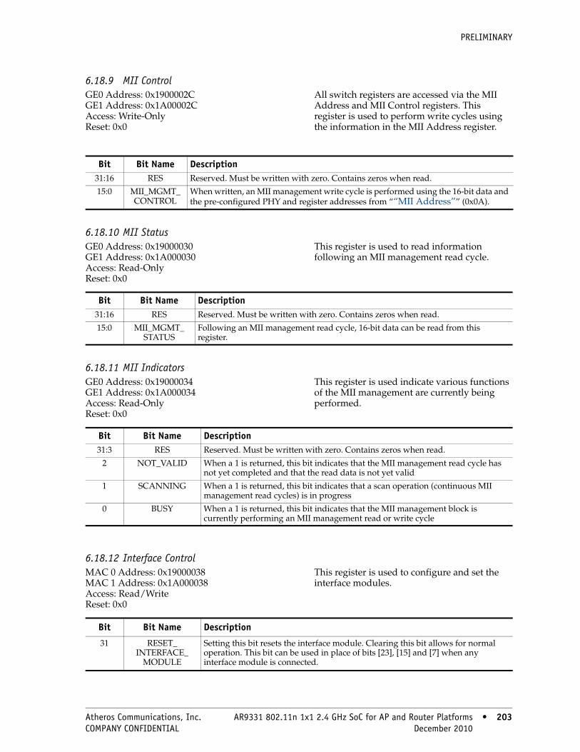
PRELIMINARY
6.18.9 MII ControlGE0 Address: 0x1900002CGE1 Address: 0x1A00002C Access: Write-Only Reset: 0x0
All switch registers are accessed via the MII Address and MII Control registers. This register is used to perform write cycles using the information in the MII Address register.
6.18.10 MII StatusGE0 Address: 0x19000030GE1 Address: 0x1A000030 Access: Read-Only Reset: 0x0
This register is used to read information following an MII management read cycle.
6.18.11 MII IndicatorsGE0 Address: 0x19000034GE1 Address: 0x1A000034 Access: Read-Only Reset: 0x0
This register is used indicate various functions of the MII management are currently being performed.
6.18.12 Interface ControlMAC 0 Address: 0x19000038 MAC 1 Address: 0x1A000038 Access: Read/Write Reset: 0x0
This register is used to configure and set the interface modules.
Bit Bit Name Description31:16 RES Reserved. Must be written with zero. Contains zeros when read.
15:0 MII_MGMT_ CONTROL
When written, an MII management write cycle is performed using the 16-bit data and the pre-configured PHY and register addresses from ““MII Address”” (0x0A).
Bit Bit Name Description31:16 RES Reserved. Must be written with zero. Contains zeros when read.
15:0 MII_MGMT_ STATUS
Following an MII management read cycle, 16-bit data can be read from this register.
Bit Bit Name Description31:3 RES Reserved. Must be written with zero. Contains zeros when read.
2 NOT_VALID When a 1 is returned, this bit indicates that the MII management read cycle has not yet completed and that the read data is not yet valid
1 SCANNING When a 1 is returned, this bit indicates that a scan operation (continuous MII management read cycles) is in progress
0 BUSY When a 1 is returned, this bit indicates that the MII management block is currently performing an MII management read or write cycle
Bit Bit Name Description
31 RESET_ INTERFACE_
MODULE
Setting this bit resets the interface module. Clearing this bit allows for normal operation. This bit can be used in place of bits [23], [15] and [7] when any interface module is connected.
Atheros Communications, Inc. AR9331 802.11n 1x1 2.4 GHz SoC for AP and Router Platforms • 203 COMPANY CONFIDENTIAL December 2010 • 203

PRELIMINARY
6.18.13 Interface StatusGE0 Address: 0x1900003C GE1 Address: 0x1A00003C Access: Read-Only Reset: 0x0
Identifies the interface statuses. The range of bits that are active are dependant upon the optional interfaces connected at the time.
30:28 RES Reserved. Must be written with zero. Contains zeros when read.
27 TBIMODE Setting this bit configures the A-RGMII module to expect TBI signals at the GMII interface. This bit should not be asserted unless this mode is being used.
26 GHDMODE Setting this bit configures the A-RGMII to expect half-duplex at the GMII interface. It also enables the use of CRS and COL signals.
25 LHDMODE Setting this bit configures the A-RGMII module to expect 10 or 100 Mbps half-duplex MII at the GMII interface and will enable the use of CRS and COL signals. This bit should not be asserted unless this mode is being used.
24 PHY_MODE Setting this bit configures the serial MII module to be in PHY Mode. Link characteristics are taken directly from the RX segments supplied by the PHY.
23 RESET_PERMII Setting this bit resets the PERMII module. Clearing this bit allows for normal operation.
22:17 RES Reserved. Must be written with zero. Contains zeros when read.
16 SPEED This bit configures the reduced MII module with the current operating speed.
0 Selects 10 Mbps mode
1 Selects 100 Mbps mode
15 RESET_PE100X This bit resets the PE100X module, which contains the 4B/5B symbol encipher/decipher code.
14:11 RES Reserved. Must be written with zero. Contains zeros when read.
10 FORCE_QUIET Affects PE100X module only.
0 Normal operation
1 Tx data is quiet, allowing the contents of the cipher to be output
9 NO_CIPHER Affects PE100X module only.
0 Normal ciphering occurs
1 The raw transmit 5B symbols are transmitting without ciphering
8 DISABLE_LINK_ FAIL
Affects PE100X module only.
0 Normal Operation
1 Disables the 330-ms link fail timer, allowing shorter simulations. Removes the 330-ms link-up time before stream reception is allowed.
7 RESET GPSI This bit resets the PE10T module which converts MII nibble streams to the serial bit stream of ENDEC PHYs. Affects PE10T module only.
6:1 RES Reserved. Must be written with zero. Contains zeros when read.
0 ENABLE_ JABBER_
PROTECTION
This bit enables the Jabber Protection logic within the PE10T in ENDEC mode. Jabber is the condition where a transmitter is on for longer than 50 ms preventing other stations from transmitting. Affects PE10T module only.
Bit Bit Name Description31:10 RES Reserved. Must be written with zero. Contains zeros when read.
204 • AR9331 802.11n 1x1 2.4 GHz SoC for AP and Router Platforms Atheros Communications, Inc. 204 • December 2010 COMPANY CONFIDENTIAL

PRELIMINARY
6.18.14 STA Address 1GE0 Address: 0x19000040 GE1 Address: 0x1A000040 Access: Read/Write Reset: 0x0
This register holds the first four octets of the station address.
9 EXCESS_DEFER This bit sets when the MAC excessively defers a transmission. It clears when read. This bit latches high.
8 CLASH Used to identify the serial MII module mode0 In PHY mode or in a properly configured MAC to MAC mode1 MAC to MAC mode with the partner in 10 Mbps and/or half-duplex
mode indicative of a configuration error7 JABBER Used to identify a jabber condition as detected by the serial MII PHY
0 No jabber condition detected1 Jabber condition detected
6 LINK_OK Used to identify the validity of a serial MII PHY link0 No valid link detected1 Valid link detected
5 FULL_DUPLEX Used to identify the current duplex of the serial MII PHY0 Half-duplex1 Full-duplex
4 SPEED Used to identify the current running speed of the serial MII PHY0 10 Mbps1 100 Mbps
3 LINK_FAIL Used to read the PHY link fail register. For asynchronous host accesses, this bit must be read at least once every scan read cycle of the PHY.
0 The MII management module has read the PHY link fail register to be 01 The MII management module has read the PHY link fail register to be 1
2 CARRIER_LOSS Carrier status. This bit latches high.0 No carrier loss detection1 Loss of carrier detection
1 SQE_ERROR 0 Has not detected an SQE error. Latches high.1 Has detected an SQE error.
0 JABBER 0 Has not detected a Jabber condition. Latches high.1 Has detected a Jabber condition
Bit Bit Name Description31:24 STATION_
ADDRESS_1This field holds the first octet of the station address
23:16 STATION_ ADDRESS_2
This field holds the second octet of the station address
15:8 STATION_ ADDRESS_3
This field holds the third octet of the station address
7:0 STATION_ ADDRESS_4
This field holds the fourth octet of the station address
Atheros Communications, Inc. AR9331 802.11n 1x1 2.4 GHz SoC for AP and Router Platforms • 205 COMPANY CONFIDENTIAL December 2010 • 205

PRELIMINARY
6.18.15 STA Address 2GE0 Address: 0x19000044 GE1 Address: 0x1A000044 Access: Read/Write Reset: 0x0
This register holds the last two octets of the station address.
6.18.16 ETH Configuration 0GE0 Address: 0x19000048 GE1 Address: 0x1A000048 Access: See field description Reset: 0x0
This register is used to assert and negate functions concerning the ETH module.
6.18.17 ETH Configuration 1GE0 Address: 0x1900004C GE1 Address: 0x1A00004C Access: Read/Write Reset: See field description
This register is used to configure the ETH storage area.
Bit Bit Name Description31:24 STATION_ ADDRESS_5 This field holds the fifth octet of the station address
23:16 STATION_ ADDRESS_6 This field holds the sixth octet of the station address
15:0 RES Reserved
Bit Bit Name Access Description31:13 RES RO Reserved. Must be written with zero. Contains zeros when read.
12 FTFENREQ RW Enable the FIFOsFIFOs start out as 0x1F and must be written to 0x0.11 STFENREQ RW
10 FRFENREQ RW
9 SRFENREQ RW
8 WTMENREQ RW
7:5 RES RW Reserved. Must be written with zero. Contains zeros when read.
4 HSTRSTFT RW Put the FIFOs into resetFIFOs start out as 0x1F and must be written to 0x0.3 HSTRSTST RW
2 HSTRSTFR RW
1 HSTRSTSR RW
0 HSTRSTWT RW
Bit Bit Name Reset Description31:28 RES 0x0 Reserved. Must be written with zero. Contains zeros when read.
27:16 CFGFRTH [11:0] 0xFFFF This hex value represents the minimum number of 4-byte locations to store simultaneously in the receive RAM, relative to the beginning of the frame being input, before FRRDY may be asserted. Note that FRRDY will be latent a certain amount of time due to fabric transmit clock to system transmit clock time domain crossing, and conditional on FRACPT assertion. When set to the maximum value, FRRD may be asserted only after the completion of the input frame. The value of this register must be greater than 18D when HSTDRPLT64 is asserted.
15:0 CFGXOFFRTX 0xFFFF This hexadecimal value represents the number of pause quanta (64-bit times) after an XOFF pause frame has been acknowledged until the ETH reasserts TCRQ if the ETH receive storage level has remained higher than the low watermark.
206 • AR9331 802.11n 1x1 2.4 GHz SoC for AP and Router Platforms Atheros Communications, Inc. 206 • December 2010 COMPANY CONFIDENTIAL

PRELIMINARY
6.18.18 ETH Configuration 2MAC 0 Address: 0x19000050 MAC 1 Address: 0x1A000050 Access: Read/Write Reset: See field description
This register is used to number the minimum amount of 8-byte words in the Rx RAM before pause frames are transmitted.
6.18.19 ETH Configuration 3GE0 Address: 0x19000054 GE1 Address: 0x1A000054 Access: Read/Write Reset: See field description
This register is used denote the minimum number of 4-byte locations to simultaneously store in the Tx RAM before assertion.
Bit Bit Name Reset Description
31:29 RES 0x0 Reserved. Must be written with zero. Contains zeros when read.
28:16 CFGHWM [12:0] 0xAAA This hex value represents the maximum number of 8-byte words to store simultaneously in the Rx RAM before TCRQ and PSVAL facilitates an XOFF pause control frame.
15:13 RES 0x0 Reserved. Must be written with zero. Contains zeros when read.
12:0 CFGLWM [12:0] 0x555 This hex value represents the minimum number of 8-byte words to store simultaneously in the Rx RAM before TCRQ and PSVAL facilitate an XON pause control frame in response to a previously transmitted XOFF pause control frame.
Bit Bit Name Type Reset Description
31:28 RES RO 0x0 Reserved. Must be written with zero. Contains zeros when read.
27:16 CFGHWMFT [11:0]
RW 0x555 This hex value represents the maximum number of 4-byte locations to store simultaneously in the Tx RAM before FTHWM is asserted. Note that FTHWM has two FTCLK clock periods of latency before assertion or negation, as should be considered when calculating headroom required for maximum size packets.
15:12 RES RO 0x0 Reserved. Must be written with zero. Contains zeros when read.
11:0 CFGFTTTH [11:0] RW 0xFFF This hex value represents the minimum number of 4-byte locations to store simultaneously in the Tx RAM, relative to the beginning of the frame being input, before TPSF is asserted. Note that TPSF is latent for a certain amount of time due to fabric Tx clock system Tx clock time domain crossing. When set to the maximum value, TPSF asserts only after the completion of the input frame.
Atheros Communications, Inc. AR9331 802.11n 1x1 2.4 GHz SoC for AP and Router Platforms • 207 COMPANY CONFIDENTIAL December 2010 • 207

PRELIMINARY
6.18.20 ETH Configuration 4GE0 Address: 0x19000058 GE1 Address: 0x1A000058 Access: Read/Write Reset: 0x0
This register is used to signal drop frame conditions internal to the Ethernet.
Bit Bit Name Description
31:18 RES Reserved. Must be written with zero. Contains zeros when read.
17 Unicast MAC address match
In combination with “ETH Configuration 5”, bits [17:0] of this register control which frames are dropped and which are sent to the DMA engine. If the bit is set in “ETH Configuration 5” and it does not match the value in this bit, then the frame is dropped.
16 Truncated frame
15 VLAN tag
14 Unsupported op-code
13 Pause frame
12 Control frame
11 Long event
10 Dribble nibble
9 Broadcast
8 Multicast
7 OK
6 Out of range
5 Length mismatch
4 CRC error
3 Code error
2 False carrier
1 RX_DV event
0 Drop event
208 • AR9331 802.11n 1x1 2.4 GHz SoC for AP and Router Platforms Atheros Communications, Inc. 208 • December 2010 COMPANY CONFIDENTIAL
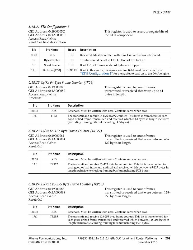
PRELIMINARY
6.18.21 ETH Configuration 5GE0 Address: 0x1900005C GE1 Address: 0x1A00005C Access: Read/Write Reset: See field description
This register is used to assert or negate bits of the ETH component.
6.18.22 Tx/Rx 64 Byte Frame Counter (TR64)GE0 Address: 0x19000080 GE1 Address: 0x1A000080 Access: Read/Write Reset: 0x0
This register is used to count frames transmitted or received that were up to 64 bytes in length.
6.18.23 Tx/Rx 65-127 Byte Frame Counter (TR127)GE0 Address: 0x19000084 GE1 Address: 0x1A000084 Access: Read/Write Reset: 0x0
This register is used to count frames transmitted or received that were between 65–127 bytes in length.
6.18.24 Tx/Rx 128-255 Byte Frame Counter (TR255)GE0 Address: 0x19000088 GE1 Address: 0x1A000088 Access: Read/Write Reset: 0x0
This register is used to count frames transmitted or received that were between 128–255 bytes in length.
Bit Bit Name Reset Description
31:20 RES 0x0 Reserved. Must be written with zero. Contains zeros when read.
19 Byte/Nibble 0x0 This bit should be set to 1 for GE0 or set to 0 for GE1.
18 Short Frame 0x0 If set to 1, all frames under 64 bytes are dropped.
17:0 Rx Filter[17:0] 0x3FFFF If set in this vector, the corresponding field must match exactly in “ETH Configuration 4” for the packet to pass on to the DMA engine.
Bit Bit Name Description
31:18 RES Reserved. Must be written with zero. Contains zeros when read.
17:0 TR64 The transmit and receive 64 byte frame counter. This bit is incremented for each good or bad frame transmitted and received which is 64 bytes in length inclusive (excluding framing bits but including FCS bytes).
Bit Bit Name Description
31:18 RES Reserved. Must be written with zero. Contains zeros when read.
17:0 TR127 The transmit and receive 65–127 byte frame counter. This bit is incremented for each good or bad frame transmitted and received which between 65-127 bytes in length inclusive (excluding framing bits but including FCS bytes).
Bit Bit Name Description31:18 RES Reserved. Must be written with zero. Contains zeros when read.
17:0 TR255 The transmit and receive 128-255 byte frame counter. This bit is incremented for each good or bad frame transmitted and received which between 128-255 bytes in length inclusive (excluding framing bits but including FCS bytes).
Atheros Communications, Inc. AR9331 802.11n 1x1 2.4 GHz SoC for AP and Router Platforms • 209 COMPANY CONFIDENTIAL December 2010 • 209

PRELIMINARY
6.18.25 Tx/Rx 256-511 Byte Frame Counter (TR511)GE0 Address: 0x1900008C GE1 Address: 0x1A00008C Access: Read/Write Reset: 0x0
This register is used to count frames transmitted or received that were between 256–511 bytes in length.
6.18.26 Tx/Rx 512-1023 Byte Frame Counter (TR1K)GE0 Address: 0x19000090 GE1 Address: 0x1A000090 Access: Read/Write Reset: 0x0
This register is used to count frames transmitted or received that were between 512–1023 bytes in length.
6.18.27 Tx/Rx 1024-1518 Byte Frame Counter (TRMAX)GE0 Address: 0x19000094 GE1 Address: 0x1A000094 Access: Read/Write Reset: 0x0
This register is used to count frames transmitted or received that were between 1024–1518 bytes in length.
6.18.28 Tx/Rx 1519-1522 Byte VLAN Frame Counter (TRMGV)GE0 Address: 0x19000098 GE1 Address: 0x1A000098 Access: Read/Write Reset: 0x0
This register is used to count frames transmitted or received that were between 1519–1522 bytes in length.
Bit Bit Name Description31:18 RES Reserved. Must be written with zero. Contains zeros when read.
17:0 TR511 The transmit and receive 256–511 byte frame counter. This bit is incremented for each good or bad frame transmitted and received which between 256–511 bytes in length inclusive (excluding framing bits but including FCS bytes).
Bit Bit Name Description
31:18 RES Reserved. Must be written with zero. Contains zeros when read.
17:0 TR1K The transmit and receive 512–1023 byte frame counter. This bit is incremented for each good or bad frame transmitted and received which between 512–1023 bytes in length inclusive (excluding framing bits but including FCS bytes).
Bit Bit Name Description
31:18 RES Reserved. Must be written with zero. Contains zeros when read.
17:0 TRMAX The transmit and receive 1024-1518 byte frame counter. This bit is incremented for each good or bad frame transmitted and received which between 1024-1518 bytes in length inclusive (excluding framing bits but including FCS bytes).
Bit Bit Name Description31:18 RES Reserved. Must be written with zero. Contains zeros when read.
17:0 TRMGV The transmit and receive 1519–1522 byte frame counter. This bit is incremented for each good or bad frame transmitted and received which between 1519–1522 bytes in length inclusive (excluding framing bits but including FCS bytes).
210 • AR9331 802.11n 1x1 2.4 GHz SoC for AP and Router Platforms Atheros Communications, Inc. 210 • December 2010 COMPANY CONFIDENTIAL

PRELIMINARY
6.18.29 Receive Byte Counter (RYBT)GE0 Address: 0x1900009C GE1 Address: 0x1A00009C Access: Read/Write Reset: 0x0
This register is used to count incoming frames and then increment this register accordingly.
6.18.30 Receive Packet Counter (RPKT)GE0 Address: 0x190000A0 GE1 Address: 0x1A0000A0
Access: Read/Write Reset: 0x0
This register is used to count packets received.
6.18.31 Receive FCS Error Counter (RFCS)GE0 Address: 0x190000A4 GE1 Address: 0x1A0000A4 Access: Read/Write Reset: 0x0
This register is used to count frames received between 64–1518 in length and has a FCS error.
6.18.32 Receive Multicast Packet Counter (RMCA)GE0 Address: 0x190000A8 GE1 Address: 0x1A0000A8 Access: Read/Write Reset: 0x0
This register is used to count received good standard multicast packets.
Bit Bit Name Description31:24 RES Reserved. Must be written with zero. Contains zeros when read.
23:0 RBYT The receive byte counter. This statistic count register is incremented by the byte count of all frames received, including bad packets but excluding framing bits but including FCS bytes.
Bit Bit Name Description
31:18 RES Reserved. Must be written with zero. Contains zeros when read.
17:0 RPKT The receive packet counter. This register is incremented for each received packet (including bad packets, all Unicast, broadcast and Multicast packets).
Bit Bit Name Description
31:12 RES Reserved. Must be written with zero. Contains zeros when read.
11:0 RFCS The received FCS error counter. This register is incremented for each frame received that has an integral 64–1518 length and contains a frame check sequence error.
Bit Bit Name Description
31:18 RES Reserved. Must be written with zero. Contains zeros when read.
17:0 RMCA The receive multicast packet counter. This register is incremented for each multicast good frame of lengths smaller than 1518 (non-VLAN) or 1522 (VLAN) excluding broadcast frames. This does not include range/length errors.
Atheros Communications, Inc. AR9331 802.11n 1x1 2.4 GHz SoC for AP and Router Platforms • 211 COMPANY CONFIDENTIAL December 2010 • 211
PRELIMINARY
6.18.33 Receive Broadcast Packet Counter (RBCA)GE0 Address: 0x190000AC GE1 Address: 0x1A0000AC Access: Read/Write Reset: 0x0
This register is used to count received good broadcast frames.
6.18.34 Receive Control Frame Packet Counter (RXCF)GE0 Address: 0x190000B0 GE1 Address: 0x1A0000B0 Access: Read/Write Reset: 0x0
This register is used to count received MAC control frames.
6.18.35 Receive Pause Frame Packet Counter (RXPF)GE0 Address: 0x190000B4 GE1 Address: 0x1A0000B4 Access: Read/Write Reset: 0x0
This register is used to count received pause frame packets.
6.18.36 Receive Unknown OPCode Packet Counter (RXUO)GE0 Address: 0x190000B8 GE1 Address: 0x1A0000B8 Access: Read/Write Reset: 0x0
This register is used to count received MAC control frames that contain an opcode.
Bit Bit Name Description
31:22 RES Reserved. Must be written with zero. Contains zeros when read.
21:0 RBCA The receive broadcast packet counter. This register is incremented for each broadcast good frame of lengths smaller than 1518 (non-VLAN) or 1522 (VLAN) excluding multicast frames. This does not include range or length errors.
Bit Bit Name Description
31:18 RES Reserved. Must be written with zero. Contains zeros when read.
17:0 RXCF The receive control frame packet counter. This register is incremented for each MAC control frame received (pause and unsupported).
Bit Bit Name Description
31:12 RES Reserved. Must be written with zero. Contains zeros when read.
11:0 RXPF The receive pause frame packet counter. This register is incremented each time a valid pause MAC control frame is received.
Bit Bit Name Description
31:12 RES Reserved. Must be written with zero. Contains zeros when read.
11:0 RXUO The receive unknown OPcode counter. This bit is incremented each time a MAC control frame is received which contains an opcode other than a pause.
212 • AR9331 802.11n 1x1 2.4 GHz SoC for AP and Router Platforms Atheros Communications, Inc. 212 • December 2010 COMPANY CONFIDENTIAL

PRELIMINARY
6.18.37 Receive Alignment Error Counter (RALN)GE0 Address: 0x190000BC GE1 Address: 0x1A0000BC Access: Read/Write Reset: 0x0
This register is used to count received packets with an alignment error.
6.18.38 Receive Frame Length Error Counter (RFLR)GE0 Address: 0x190000C0 GE1 Address: 0x1A0000C0 Access: Read/Write Reset: 0x0
This register is used to count received frames that have a length error.
6.18.39 Receive Code Error Counter (RCDE)GE0 Address: 0x190000C4 GE1 Address: 0x1A0000C4 Access: Read/Write Reset: 0x0
This register is used to count the number of received frames that had a code error counter.
6.18.40 Receive Carrier Sense Error Counter (RCSE)GE0 Address: 0x190000C8 GE1 Address: 0x1A0000C8 Access: Read/Write Reset: 0x0
This register is used to count the number of frames received that had a false carrier.
Bit Bit Name Description
31:12 RES Reserved. Must be written with zero. Contains zeros when read.
11:0 RALN The receive alignment error counter. This register is incremented for each received frame from 64–1518 bytes that contains an invalid FCS and is not an integral number of bytes.
Bit Bit Name Description31:16 RES Reserved. Must be written with zero. Contains zeros when read.
15:0 RFLR The received frame length error counter. this register is incremented for each received frame in which the 802.3 length field did not match the number of data bytes actually received (46–1500 bytes). The counter is not incremented if the length field is not a valid 802.3 length, such as an EtherType value.
Bit Bit Name Description31:12 RES Reserved. Must be written with zero. Contains zeros when read.
11:0 RCDE The receive code error counter. This register is incremented each time a valid carrier was present and at least one invalid data symbol was detected.
Bit Bit Name Description31:12 RES Reserved. Must be written with zero. Contains zeros when read.
11:0 RCSE The receive false carrier counter. This register is incremented each time a false carrier is detected during idle, as defined by a 1 on RX_ER and an 0xE on RXD. This event is reported along with the statistics generated on the next received frame. Only one false carrier condition can be detected and logged between frames.
Atheros Communications, Inc. AR9331 802.11n 1x1 2.4 GHz SoC for AP and Router Platforms • 213 COMPANY CONFIDENTIAL December 2010 • 213
PRELIMINARY
6.18.41 Receive Undersize Packet Counter (RUND)GE0 Address: 0x190000CC GE1 Address: 0x1A0000CC Access: Read/Write Reset: 0x0
This register is used to count the number of received packets that were undersized.
6.18.42 Receive Oversize Packet Counter (ROVR)GE0 Address: 0x190000D0 GE1 Address: 0x1A0000D0 Access: Read/Write Reset: 0x0
This register is used to count received packets that were oversized.
6.18.43 Receive Fragments Counter (RFRG)GE0 Address: 0x190000D4 GE1 Address: 0x1A0000D4 Access: Read/Write Reset: 0x0
This register is used to count received fragmented frames.
6.18.44 Receive Jabber Counter (RJBR)GE0 Address: 0x190000D8 GE1 Address: 0x1A0000D8 Access: Read/Write Reset: 0x0
This register is used to count received jabber frames.
Bit Bit Name Description31:12 RES Reserved. Must be written with zero. Contains zeros when read.
11:0 RUND The receive undersize packet counter. This register is incremented each time a frame is received which is less than 64 bytes in length and contains a valid FCS and were otherwise well formed. This does not include Range Length errors
Bit Bit Name Description31:12 RES Reserved. Must be written with zero. Contains zeros when read.
11:0 ROVR The receive oversize packet counter., This register is incremented each time a frame is received which exceeded 1518 (non-VLAN) or 1522 (VLAN) and contains a valid FCS and were otherwise well formed. This does not include Range Length errors.
Bit Bit Name Description31:12 RES Reserved. Must be written with zero. Contains zeros when read.
11:0 RFRG The receive fragments counter. This register is incremented for each frame received which is less than 64 bytes in length and contains an invalid FCS. This includes integral and non-integral lengths.
Bit Bit Name Description31:12 RES Reserved. Must be written with zero. Contains zeros when read.
11:0 RJBR The received jabber counter. This register is incremented for frames which exceed 1518 (non-VLAN) or 1522 (VLAN) bytes and contains an invalid FCS, including alignment errors.
214 • AR9331 802.11n 1x1 2.4 GHz SoC for AP and Router Platforms Atheros Communications, Inc. 214 • December 2010 COMPANY CONFIDENTIAL

PRELIMINARY
6.18.45 Receive Dropped Packet Counter (RDRP)GE0 Address: 0x190000DC GE1 Address: 0x1A0000DC Access: Read/Write Reset: 0x0
This register is used to count received dropped packets.
6.18.46 Transmit Byte Counter (TBYT)GE0 Address: 0x190000E0 GE1 Address: 0x1A0000E0 Access: Read/Write Reset: 0x0
This register is used to count transmitted bytes.
6.18.47 Transmit Packet Counter (TPKT)GE0 Address: 0x190000E4 GE1 Address: 0x1A0000E4 Access: Read/Write Reset: 0x0
This register is used to count transmitted packets.
6.18.48 Transmit Multicast Packet Counter (TMCA)GE0 Address: 0x190000E8 GE1 Address: 0x1A0000E8 Access: Read/Write Reset: 0x0
This register is used to count transmitted multicast packets.
Bit Bit Name Description31:12 RES Reserved. Must be written with zero. Contains zeros when read.
11:0 RDRP The received dropped packets counter. this register is incremented for frames received which are streamed to the system but are later dropped due to a lack of system resources.
Bit Bit Name Description
31:24 RES Reserved. Must be written with zero. Contains zeros when read.
23:0 TYBT The transmit byte counter. This register is incremented by the number of bytes that were put on the wire including fragments of frames that were involved with collisions. This count does not include preamble/SFD or jam bytes.
Bit Bit Name Description
31:18 RES Reserved. Must be written with zero. Contains zeros when read.
17:0 TPKT The transmit packet counter. This register is incremented for each transmitted packet (including bad packets, excessive deferred packets, excessive collision packets, late collision packets, all Unicast, Broadcast and Multicast packets.
Bit Bit Name Description
31:18 RES Reserved. Must be written with zero. Contains zeros when read.
17:0 TMCA Transmit multicast packet counter. Incremented for each multicast valid frame transmitted (excluding broadcast frames).
Atheros Communications, Inc. AR9331 802.11n 1x1 2.4 GHz SoC for AP and Router Platforms • 215 COMPANY CONFIDENTIAL December 2010 • 215

PRELIMINARY
6.18.49 Transmit Broadcast Packet Counter (TBCA)GE0 Address: 0x190000EC GE1 Address: 0x1A0000EC Access: Read/Write Reset: 0x0
This register is used to count transmitted broadcast packets.
6.18.50 Transmit Pause Control Frame Counter (TXPF)GE0 Address: 0x190000F0 GE1 Address: 0x1A0000F0 Access: Read/Write Reset: 0x0
This register is used to count transmitted pause control frames.
6.18.51 Transmit Deferral Packet Counter (TDFR)GE0 Address: 0x190000F4 GE1 Address: 0x1A0000F4 Access: Read/Write Reset: 0x0
This register is used to count transmitted deferral packets.
6.18.52 Transmit Excessive Deferral Packet Counter (TEDF)GE0 Address: 0x190000F8 GE1 Address: 0x1A0000F8 Access: Read/Write Reset: 0x0
This register is used to count excessive transmitted deferral packets.
Bit Bit Name Description
31:18 RES Reserved. Must be written with zero. Contains zeros when read.
17:0 TBCA Transmit broadcast packet counter. Incremented for each broadcast frame transmitted (excluding multicast frames).
Bit Bit Name Description
31:12 RES Reserved. Must be written with zero. Contains zeros when read.
11:0 TXPF Transmit pause frame packet counter. Incremented each time a valid pause MAC control frame is transmitted.
Bit Bit Name Description
31:12 RES Reserved. Must be written with zero. Contains zeros when read.
11:0 TDFR Transmit deferral packet counter. Incremented for each frame that was deferred on its first transmission attempt. Does not include frames involved in collisions.
Bit Bit Name Description
31:12 RES Reserved. Must be written with zero. Contains zeros when read.
11:0 TEDF Transmit excessive deferral packet counter. Incremented for frames aborted that were deferred for an excessive period of time (3036 byte times).
216 • AR9331 802.11n 1x1 2.4 GHz SoC for AP and Router Platforms Atheros Communications, Inc. 216 • December 2010 COMPANY CONFIDENTIAL

PRELIMINARY
6.18.53 Transmit Single Collision Packet Counter (TSCL)GE0 Address: 0x190000FC GE1 Address: 0x1A0000FC Access: Read/Write Reset: 0x0
This register is used to count transmitted single collision packets.
6.18.54 Transmit Multiple Collision Packet (TMCL)GE0 Address: 0x19000100 GE1 Address: 0x1A000100 Access: Read/Write Reset: 0x0
This register is used to count transmitted multiple collision packets.
6.18.55 Transmit Late Collision Packet Counter (TLCL)GE0 Address: 0x19000104 GE1 Address: 0x1A000104 Access: Read/Write Reset: 0x0
This register is used to count transmitted late collision packets.
6.18.56 Transmit Excessive Collision Packet Counter (TXCL)GE0 Address: 0x19000108 GE1 Address: 0x1A000108 Access: Read/Write Reset: 0x0
This register is used to count excessive transmitted collision packets.
Bit Bit Name Description
31:12 RES Reserved. Must be written with zero. Contains zeros when read.
11:0 TSCL Transmit single collision packet counter. Incremented for each frame transmitted that experienced exactly one collision during transmission.
Bit Bit Name Description31:12 RES Reserved. Must be written with zero. Contains zeros when read.
11:0 TMCL Tx multiple collision packet counter. Incremented for each frame transmitted that experienced 2–15 collisions (including any late collisions) during transmission as defined using the RETRY[3:0] field of the Tx function control register.
Bit Bit Name Description31:12 RES Reserved. Must be written with zero. Contains zeros when read.
11:0 TLCL Transmit late collision packet counter. Incremented for each frame transmitted that experienced a late collision during a transmission attempt. Late collisions are defined using the LCOL[5:0] field of the Tx function control register.
Bit Bit Name Description31:12 RES Reserved. Must be written with zero. Contains zeros when read.
11:0 TXCL Transmit excessive collision packet counter. Incremented for each frame that experienced 16 collisions during transmission and was aborted.
Atheros Communications, Inc. AR9331 802.11n 1x1 2.4 GHz SoC for AP and Router Platforms • 217 COMPANY CONFIDENTIAL December 2010 • 217
PRELIMINARY
6.18.57 Transmit Total Collision Counter (TNCL)GE0 Address: 0x1900010C GE1 Address: 0x1A00010C Access: Read/Write Reset: 0x0
This register is used to count transmitted total collision packets.
6.18.58 Transmit Pause Frames Honored Counter (TPFH)GE0 Address: 0x19000110 GE1 Address: 0x1A000110 Access: Read/Write Reset: 0x0
This register is used to count honored transmitted pause frames.
6.18.59 Transmit Drop Frame Counter (TDRP)GE0 Address: 0x19000114 GE1 Address: 0x1A000114 Access: Read/Write Reset: 0x0
This register is used to count transmitted drop frames.
6.18.60 Transmit Jabber Frame Counter (TJBR)GE0 Address: 0x19000118 GE1 Address: 0x1A000118 Access: Read/Write Reset: 0x0
This register is used to count transmitted jabber frames.
Bit Bit Name Description31:13 RES Reserved. Must be written with zero. Contains zeros when read.
12:0 TNCL Transmit total collision counter. Incremented by the number of collisions experienced during the transmission of a frame as defined as the simultaneous presence of signals on the DO and RD circuits (i.e., transmitting and receiving at the same time). Note, this register does not include collisions that result in an excessive collision condition).
Bit Bit Name Description
31:12 RES Reserved. Must be written with zero. Contains zeros when read.
11:0 TPFH Transmit pause frames honored counter. Incremented each time a valid pause MAC control frame is transmitted and honored.
Bit Bit Name Description
31:12 RES Reserved. Must be written with zero. Contains zeros when read.
11:0 TDRP Transmit drop frame counter. Incremented each time input PFH is asserted.
Bit Bit Name Description
31:12 RES Reserved. Must be written with zero. Contains zeros when read.
11:0 TJBR Transmit jabber frame counter. Incremented for each oversized transmitted frame with an incorrect FCS value.
218 • AR9331 802.11n 1x1 2.4 GHz SoC for AP and Router Platforms Atheros Communications, Inc. 218 • December 2010 COMPANY CONFIDENTIAL

PRELIMINARY
6.18.61 Transmit FCS Error Counter (TFCS)GE0 Address: 0x1900011C GE1 Address: 0x1A00011C Access: Read/Write Reset: 0x0
This register is used to count transmitted FCS errors.
6.18.62 Transmit Control Frame Counter (TXCF)GE0 Address: 0x19000120 GE1 Address: 0x1A000120 Access: Read/Write Reset: 0x0
This register is used to count transmitted control frames.
6.18.63 Transmit Oversize Frame Counter (TOVR)GE0 Address: 0x19000124 GE1 Address: 0x1A000124000128 Access: Read/Write Reset: 0x0
This register is used to count transmitted oversize frames.
6.18.64 Transmit Undersize Frame Counter (TUND)GE0 Address: 0x19000128 GE1 Address: 0x1A000128 Access: Read/Write Reset: 0x0
This register is used to count transmitted undersize frames.
Bit Bit Name Description
31:12 RES Reserved. Must be written with zero. Contains zeros when read.
11:0 TFCS Transmit FCS error counter. Incremented for every valid sized packet with an incorrect FCS value.
Bit Bit Name Description
31:12 RES Reserved. Must be written with zero. Contains zeros when read.
11:0 TXCF Transmit control frame counter. Incremented for every valid size frame with a type field signifying a control frame.
Bit Bit Name Description
31:12 RES Reserved. Must be written with zero. Contains zeros when read.
11:0 TOVR Transmit oversize frame counter. Incremented for each oversized transmitted frame with an correct FCS value.
Bit Bit Name Description
31:12 RES Reserved. Must be written with zero. Contains zeros when read.
11:0 TUND Transmit undersize frame counter. Incremented for every frame less then 64 bytes, with a correct FCS value.
Atheros Communications, Inc. AR9331 802.11n 1x1 2.4 GHz SoC for AP and Router Platforms • 219 COMPANY CONFIDENTIAL December 2010 • 219

PRELIMINARY
6.18.65 Transmit Fragment Counter (TFRG)GE0 Address: 0x1900012C GE1 Address: 0x1A00012C Access: Read/Write Reset: 0x0
This register is used to count transmitted fragments.
6.18.66 Carry Register 1 (CAR1)GE0 Address: 0x19000130 GE1 Address: 0x1A000130 Access: Read-Only Reset: 0x0
Carry register bits are cleared on carry register write while the respective bit is asserted.
Bit Bit Name Description
31:12 RES Reserved. Must be written with zero. Contains zeros when read.
11:0 TFRG Transmit fragment counter. Incremented for every frame less then 64 bytes, with an incorrect FCS value.
Bit Bit Name Description
31 C1_64 Carry register 1 TR64 counter carry bit
30 C1_127 Carry register 1 TR127 counter carry bit
29 C1_255 Carry register 1 TR255 counter carry bit
28 C1_511 Carry register 1 TR511 counter carry bit
27 C1_1K Carry register 1 TR1K counter carry bit
26 C1_MAX Carry register 1 TRMAX counter carry bit
25 C1_MGV Carry register 1 TRMGV counter carry bit
24:17 RES Reserved. Must be written with zero. Contains zeros when read.
16 C1_RBY Carry register 1 RBYT counter carry bit
15 C1_RPK Carry register 1 RPKT counter carry bit
14 C1_RFC Carry register 1 RFCS counter carry bit
13 C1_RMC Carry register 1 RMCA counter carry bit
12 C1_RBC Carry register 1 RBCA counter carry bit
11 C1_RXC Carry register 1 RXCF counter carry bit
10 C1_RXP Carry register 1 RXPF counter carry bit
9 C1_RXU Carry register 1 RXUO counter carry bit
8 C1_RAL Carry register 1 RALN counter carry bit
7 C1_RFL Carry register 1 RFLR counter carry bit
6 C1_RCD Carry register 1 RCDE counter carry bit
5 C1_RCS Carry register 1 RCSE counter carry bit
4 C1_RUN Carry register 1 RUND counter carry bit
3 C1_ROV Carry register 1 ROVR counter carry bit
2 C1_RFR Carry register 1 RFRG counter carry bit
1 C1_RJB Carry register 1 RJBR counter carry bit
0 C1_RDR Carry register 1 RDRP counter carry bit
220 • AR9331 802.11n 1x1 2.4 GHz SoC for AP and Router Platforms Atheros Communications, Inc. 220 • December 2010 COMPANY CONFIDENTIAL
PRELIMINARY
6.18.67 Carry Register 2 (CAR2)GE0 Address: 0x19000134 GE1 Address: 0x1A000134 Access: Read-Only Reset: 0x0
Carry register bits are cleared on a carry register write while the respective bit is asserted.
Bit Bit Name Description
31:20 RES Reserved. Must be written with zero. Contains zeros when read.
19 C2_TJB Carry register 2 TJBR counter carry bit
18 C2_TFC Carry register 2 TFCS counter carry bit
17 C2_TCF Carry register 2 TXCF counter carry bit
16 C2_TOV Carry register 2 TOVR counter carry bit
15 C2_TUN Carry register 2 TUND counter carry bit
14 C2_TFG Carry register 2 TFRG counter carry bit
13 C2_TBY Carry register 2 TBYT counter carry bit
12 C2_TPK Carry register 2 TPKT counter carry bit
11 C2_TMC Carry register 2 TMCA counter carry bit
10 C2_TBC Carry register 2 TBCA counter carry bit
9 C2_TPF Carry register 2 TXPF counter carry bit
8 C2_TDF Carry register 2 TDFR counter carry bit
7 C2_TED Carry register 2 TEDF counter carry bit
6 C2_TSC Carry register 2 TSCL counter carry bit
5 C2_TMA Carry register 2 TMCL counter carry bit
4 C2_TLC Carry register 2 TLCL counter carry bit
3 C2_TXC Carry register 2 TXCL counter carry bit
2 C2_TNC Carry register 2 TNCL counter carry bit
1 C2_TPH Carry register 2 TPFH counter carry bit
0 C2_TDP Carry register 2 TDRP counter carry bit
Atheros Communications, Inc. AR9331 802.11n 1x1 2.4 GHz SoC for AP and Router Platforms • 221 COMPANY CONFIDENTIAL December 2010 • 221

PRELIMINARY
6.18.68 Carry Mask Register 1 (CAM1)GE0 Address: 0x19000138 GE1 Address: 0x1A000138 Access: Read/Write Reset: 0x1
When one of these mask bits is set to zero, the corresponding interrupt bit is allowed to cause interrupt indications on output CARRY.
Bit Bit NaM1e Description
31 M1_64 Mask register 1 TR64 counter carry bit
30 M1_127 Mask register 1 TR127 counter carry bit
29 M1_255 Mask register 1 TR255 counter carry bit
28 M1_511 Mask register 1 TR511 counter carry bit
27 M1_1K Mask register 1 TR1K counter carry bit
26 M1_MAX Mask register 1 TRMAX counter carry bit
25 M1_MGV Mask register 1 TRMGV counter carry bit
24:17 RES Reserved. Must be written with zero. Contains zeros when read.
16 M1_RBY Mask register 1 RBYT counter carry bit
15 M1_RPK Mask register 1 RPKT counter carry bit
14 M1_RFC Mask register 1 RFCS counter carry bit
13 M1_RMC Mask register 1 RMCA counter carry bit
12 M1_RBC Mask register 1 RBCA counter carry bit
11 M1_RXC Mask register 1 RXCF counter carry bit
10 M1_RXP Mask register 1 RXPF counter carry bit
9 M1_RXU Mask register 1 RXUO counter carry bit
8 M1_RAL Mask register 1 RALN counter carry bit
7 M1_RFL Mask register 1 RFLR counter carry bit
6 M1_RCD Mask register 1 RCDE counter carry bit
5 M1_RCS Mask register 1 RCSE counter carry bit
4 M1_RUN Mask register 1 RUND counter carry bit
3 M1_ROV Mask register 1 ROVR counter carry bit
2 M1_RFR Mask register 1 RFRG counter carry bit
1 M1_RJB Mask register 1 RJBR counter carry bit
0 M1_RDR Mask register 1 RDRP counter carry bit
222 • AR9331 802.11n 1x1 2.4 GHz SoC for AP and Router Platforms Atheros Communications, Inc. 222 • December 2010 COMPANY CONFIDENTIAL
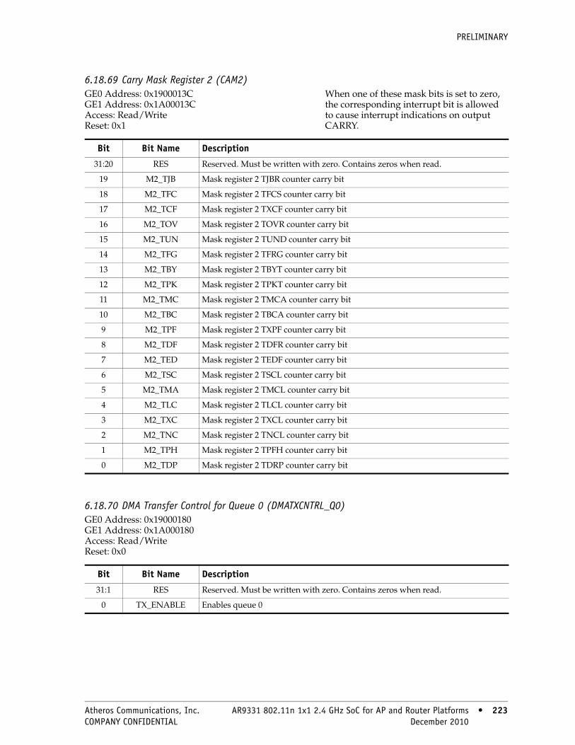
PRELIMINARY
6.18.69 Carry Mask Register 2 (CAM2)GE0 Address: 0x1900013C GE1 Address: 0x1A00013C Access: Read/Write Reset: 0x1
When one of these mask bits is set to zero, the corresponding interrupt bit is allowed to cause interrupt indications on output CARRY.
6.18.70 DMA Transfer Control for Queue 0 (DMATXCNTRL_Q0)GE0 Address: 0x19000180 GE1 Address: 0x1A000180 Access: Read/Write Reset: 0x0
Bit Bit Name Description
31:20 RES Reserved. Must be written with zero. Contains zeros when read.
19 M2_TJB Mask register 2 TJBR counter carry bit
18 M2_TFC Mask register 2 TFCS counter carry bit
17 M2_TCF Mask register 2 TXCF counter carry bit
16 M2_TOV Mask register 2 TOVR counter carry bit
15 M2_TUN Mask register 2 TUND counter carry bit
14 M2_TFG Mask register 2 TFRG counter carry bit
13 M2_TBY Mask register 2 TBYT counter carry bit
12 M2_TPK Mask register 2 TPKT counter carry bit
11 M2_TMC Mask register 2 TMCA counter carry bit
10 M2_TBC Mask register 2 TBCA counter carry bit
9 M2_TPF Mask register 2 TXPF counter carry bit
8 M2_TDF Mask register 2 TDFR counter carry bit
7 M2_TED Mask register 2 TEDF counter carry bit
6 M2_TSC Mask register 2 TSCL counter carry bit
5 M2_TMA Mask register 2 TMCL counter carry bit
4 M2_TLC Mask register 2 TLCL counter carry bit
3 M2_TXC Mask register 2 TXCL counter carry bit
2 M2_TNC Mask register 2 TNCL counter carry bit
1 M2_TPH Mask register 2 TPFH counter carry bit
0 M2_TDP Mask register 2 TDRP counter carry bit
Bit Bit Name Description
31:1 RES Reserved. Must be written with zero. Contains zeros when read.
0 TX_ENABLE Enables queue 0
Atheros Communications, Inc. AR9331 802.11n 1x1 2.4 GHz SoC for AP and Router Platforms • 223 COMPANY CONFIDENTIAL December 2010 • 223
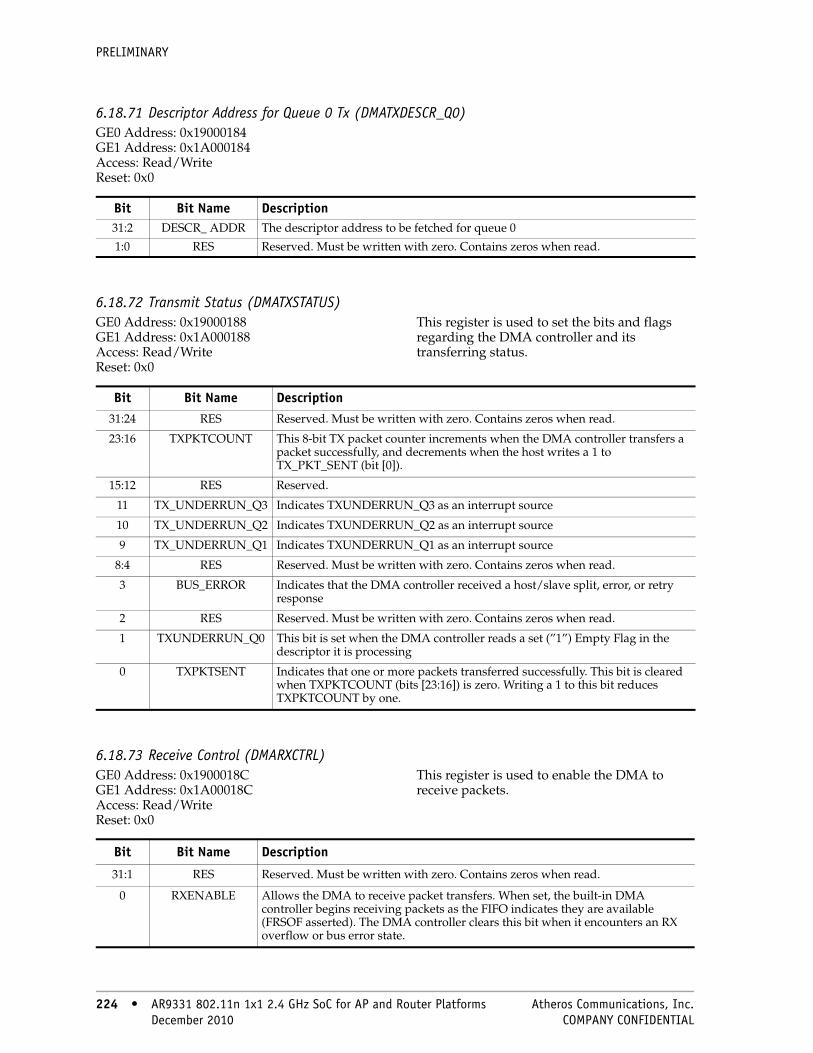
PRELIMINARY
6.18.71 Descriptor Address for Queue 0 Tx (DMATXDESCR_Q0)GE0 Address: 0x19000184 GE1 Address: 0x1A000184 Access: Read/Write Reset: 0x0
6.18.72 Transmit Status (DMATXSTATUS)GE0 Address: 0x19000188 GE1 Address: 0x1A000188 Access: Read/Write Reset: 0x0
This register is used to set the bits and flags regarding the DMA controller and its transferring status.
6.18.73 Receive Control (DMARXCTRL)GE0 Address: 0x1900018C GE1 Address: 0x1A00018C Access: Read/Write Reset: 0x0
This register is used to enable the DMA to receive packets.
Bit Bit Name Description31:2 DESCR_ ADDR The descriptor address to be fetched for queue 0
1:0 RES Reserved. Must be written with zero. Contains zeros when read.
Bit Bit Name Description31:24 RES Reserved. Must be written with zero. Contains zeros when read.
23:16 TXPKTCOUNT This 8-bit TX packet counter increments when the DMA controller transfers a packet successfully, and decrements when the host writes a 1 to TX_PKT_SENT (bit [0]).
15:12 RES Reserved.
11 TX_UNDERRUN_Q3 Indicates TXUNDERRUN_Q3 as an interrupt source
10 TX_UNDERRUN_Q2 Indicates TXUNDERRUN_Q2 as an interrupt source
9 TX_UNDERRUN_Q1 Indicates TXUNDERRUN_Q1 as an interrupt source
8:4 RES Reserved. Must be written with zero. Contains zeros when read.
3 BUS_ERROR Indicates that the DMA controller received a host/slave split, error, or retry response
2 RES Reserved. Must be written with zero. Contains zeros when read.
1 TXUNDERRUN_Q0 This bit is set when the DMA controller reads a set (”1”) Empty Flag in the descriptor it is processing
0 TXPKTSENT Indicates that one or more packets transferred successfully. This bit is cleared when TXPKTCOUNT (bits [23:16]) is zero. Writing a 1 to this bit reduces TXPKTCOUNT by one.
Bit Bit Name Description
31:1 RES Reserved. Must be written with zero. Contains zeros when read.
0 RXENABLE Allows the DMA to receive packet transfers. When set, the built-in DMA controller begins receiving packets as the FIFO indicates they are available (FRSOF asserted). The DMA controller clears this bit when it encounters an RX overflow or bus error state.
224 • AR9331 802.11n 1x1 2.4 GHz SoC for AP and Router Platforms Atheros Communications, Inc. 224 • December 2010 COMPANY CONFIDENTIAL

PRELIMINARY
6.18.74 Pointer to Receive Descriptor (DMARXDESCR)GE0 Address: 0x19000190 GE1 Address: 0x1A000190 Access: Read/Write Reset: 0x0
This register is used to find the location of the first TX packet descriptor in the memory.
6.18.75 Receive Status (DMARXSTATUS)GE0 Address: 0x19000194 GE1 Address: 0x1A000194 Access: Read/Write Reset: 0x0
This register is used to set the bits and flags regarding the DMA controller and its receiving status.
Bit Bit Name Description
31:2 DESCRIPTOR_ ADDRESS
The descriptor address. When the RXENABLE (bit [0] of the “Receive Control (DMARXCTRL)” register) is set by the host, the DMA controller reads this register to find the host memory location of the first receive packet descriptor.
1:0 RES Ignored by the DMA controller, because it is a requirement of the system that all descriptors are 32-bit aligned in the host memory.
Bit Bit Name Description
31:24 RES Reserved. Must be written with zero. Contains zeros when read.
23:16 RXPKTCOUNT This 8-bit receive packet counter increments when the DMA controller transfers a packet successfully, and decrements when the host writes a 1 to RXPKTRECEIVED (bit [0]).
15:4 RES Reserved. Must be written with zero. Contains zeros when read.
3 BUSERROR Indicates that the DMA controller received a host/slave split, error, or retry response
2 RES Reserved. Must be written with zero. Contains zeros when read.
1 RXOVERFLOW This bit is set when the DMA controller reads a set empty flag in the descriptor it is processing
0 RXPKT RECEIVED
Indicates that one or more packets were received successfully. This bit is cleared when the RXPKTCOUNT (bits [23:16]) is zero. Writing a 1 to this bit reduces RXPKTCOUNT by one.
Atheros Communications, Inc. AR9331 802.11n 1x1 2.4 GHz SoC for AP and Router Platforms • 225 COMPANY CONFIDENTIAL December 2010 • 225
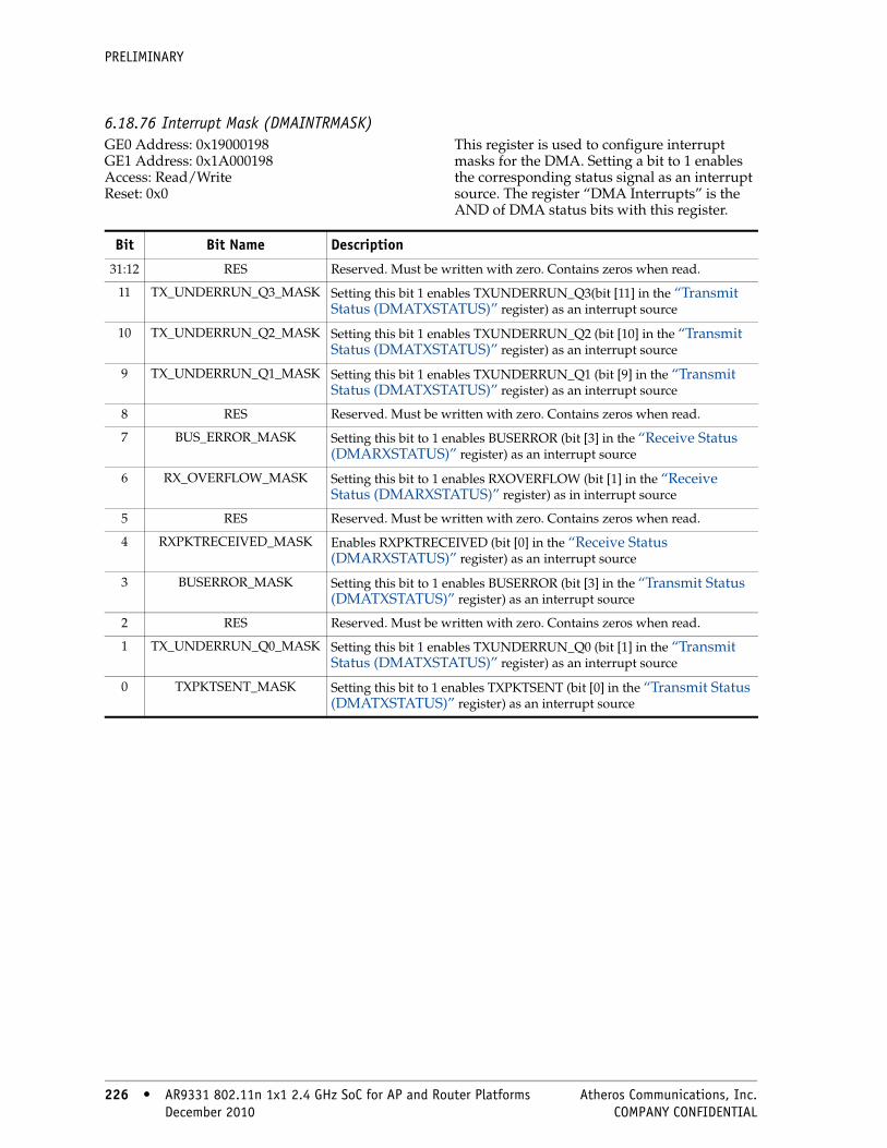
PRELIMINARY
6.18.76 Interrupt Mask (DMAINTRMASK)GE0 Address: 0x19000198 GE1 Address: 0x1A000198 Access: Read/Write Reset: 0x0
This register is used to configure interrupt masks for the DMA. Setting a bit to 1 enables the corresponding status signal as an interrupt source. The register “DMA Interrupts” is the AND of DMA status bits with this register.
Bit Bit Name Description
31:12 RES Reserved. Must be written with zero. Contains zeros when read.
11 TX_UNDERRUN_Q3_MASK Setting this bit 1 enables TXUNDERRUN_Q3(bit [11] in the “Transmit Status (DMATXSTATUS)” register) as an interrupt source
10 TX_UNDERRUN_Q2_MASK Setting this bit 1 enables TXUNDERRUN_Q2 (bit [10] in the “Transmit Status (DMATXSTATUS)” register) as an interrupt source
9 TX_UNDERRUN_Q1_MASK Setting this bit 1 enables TXUNDERRUN_Q1 (bit [9] in the “Transmit Status (DMATXSTATUS)” register) as an interrupt source
8 RES Reserved. Must be written with zero. Contains zeros when read.
7 BUS_ERROR_MASK Setting this bit to 1 enables BUSERROR (bit [3] in the “Receive Status (DMARXSTATUS)” register) as an interrupt source
6 RX_OVERFLOW_MASK Setting this bit to 1 enables RXOVERFLOW (bit [1] in the “Receive Status (DMARXSTATUS)” register) as in interrupt source
5 RES Reserved. Must be written with zero. Contains zeros when read.
4 RXPKTRECEIVED_MASK Enables RXPKTRECEIVED (bit [0] in the “Receive Status (DMARXSTATUS)” register) as an interrupt source
3 BUSERROR_MASK Setting this bit to 1 enables BUSERROR (bit [3] in the “Transmit Status (DMATXSTATUS)” register) as an interrupt source
2 RES Reserved. Must be written with zero. Contains zeros when read.
1 TX_UNDERRUN_Q0_MASK Setting this bit 1 enables TXUNDERRUN_Q0 (bit [1] in the “Transmit Status (DMATXSTATUS)” register) as an interrupt source
0 TXPKTSENT_MASK Setting this bit to 1 enables TXPKTSENT (bit [0] in the “Transmit Status (DMATXSTATUS)” register) as an interrupt source
226 • AR9331 802.11n 1x1 2.4 GHz SoC for AP and Router Platforms Atheros Communications, Inc. 226 • December 2010 COMPANY CONFIDENTIAL

PRELIMINARY
6.18.77 Interrupts (DMAINTERRUPT)GE0 Address: 0x1900019C GE1 Address: 0x1A00019C Access: Read/Write Reset: 0x0
This register is used to configure interrupts for the DMA. Flags in this register clear when their corresponding Status bit is cleared.
Bit Bit Name Description
31:12 RES Reserved. Must be written with zero. Contains zeros when read.
11 TX_UNDERRUN_Q3
Setting this bit 1 enables TXUNDERRUN_Q3(bit [11] in the “Transmit Status (DMATXSTATUS)” register) as an interrupt source
10 TX_UNDERRUN_Q2
Setting this bit 1 enables TXUNDERRUN_Q2 (bit [10] in the “Transmit Status (DMATXSTATUS)” register) as an interrupt source
9 TX_UNDERRUN_Q1
Setting this bit 1 enables TXUNDERRUN_Q1 (bit [9] in the “Transmit Status (DMATXSTATUS)” register) as an interrupt source
8 RES Reserved. Must be written with zero. Contains zeros when read.
7 BUS_ERROR_MASK
Setting this bit to 1 records an Rx bus error interrupt when BUS_ERROR (bit [3] in the “Receive Status (DMARXSTATUS)” register) and BUS_ERROR_MASK (bit [7] of the “Interrupt Mask (DMAINTRMASK)” register) are both set
6 RX_OVERFLOW_MASK
Setting this bit to 1 records an Rx overflow error interrupt when RX_OVERFLOW (bit [1] in the “Receive Status (DMARXSTATUS)” register) and RX_OVERFLOW_MASK (bit [6] of the “Interrupt Mask (DMAINTRMASK)” register) are both set
5 RES Reserved. Must be written with zero. Contains zeros when read.
4 RXPKT_ RECEIVED_
MASK
Records a RX_PKT_RECEIVED error interrupt when RX_PKT_RECEIVED (bit [0] in the “Receive Status (DMARXSTATUS)” register) and RXPKT_RECEIVED_MASK (bit [4] of the “Interrupt Mask (DMAINTRMASK)” register) are both set
3 BUS_ERROR Setting this bit to 1 enables BUSERROR (bit [3] in the “Transmit Status (DMATXSTATUS)” register) and BUSERROR_MASK (bit [3] of the “Interrupt Mask (DMAINTRMASK)” register) are both set
2 RES Reserved. Must be written with zero. Contains zeros when read.
1 TX_UNDERRUN_Q0
Setting this bit to 1 enables TX_UNDERRUN (bit [1] in the “Transmit Status (DMATXSTATUS)” register) and TX_UNDERRUN_MASK (bit [1] of the “Interrupt Mask (DMAINTRMASK)” register) are both set
0 TXPKTSENT Set this bit to 1 enables TXPKTSENT (bit [0] in the “Transmit Status (DMATXSTATUS)” register) and TXPKTSENT_MASK (bit [0] of the “Interrupt Mask (DMAINTRMASK)” register) are both set
Atheros Communications, Inc. AR9331 802.11n 1x1 2.4 GHz SoC for AP and Router Platforms • 227 COMPANY CONFIDENTIAL December 2010 • 227

PRELIMINARY
6.18.78 Ethernet Tx FIFO Throughput (ETH_TXFIFO_TH)GE0 Address: 0x190001A4 GE1 Address: 0x1A0001A4 Access: Read/Write Reset: See field description
This Ethernet register has a 2 KB Tx FIFO. It is use to determine the minimum and maximum levels of the transfer FIFO and correspondingly keep the transmit levels within the range to keep a continuous data transfer flowing.
6.18.79 Current Tx and Rx FIFO Depth (ETH_XFIFO_DEPTH)GE0 Address: 0x190001A8 GE1Address: 0x1A0001A8 Access: Read/Write Reset: 0x0
6.18.80 Ethernet Rx FIFO Threshold (ETH_RXFIFO_TH)GE0 Address: 0x190001AC GE1 Address: 0x1A0001AC Access: Read/Write Reset: See field description
This Ethernet register has a 2 KB Rx FIFO. It is used to determine the minimum and maximum levels of the transfer FIFO and correspondingly keep the transmit levels within the range to keep a continuous data transfer flowing.
Bit Bit Name Reset Description
31:26 RES 0x0 Reserved. Must be written with zero. Contains zeros when read.
25:16 TXFIFO_MAXTH 0x1D8 This bit represents the maximum number of double words in the Tx FIFO, and once this limit is surpassed, this bit should be de-asserted
15:10 RES 0x0 Reserved. Must be written with zero. Contains zeros when read.
9:0 TXFIFO_MINTH 0x160 This bit specifies the minimum number of double words in the Tx FIFO, and if it is less than this value, this bit needs to be asserted.
Bit Bit Name Description
31:26 RES Reserved
25:16 CURRENT_RX_FIFO_DEPTH Current Rx FIFO depth
15:10 RES Reserved
9:0 CURRENT_TX_FIFO_DEPTH Current Tx FIFO depth
Bit Bit Name Reset Description
31:10 SCRATCHREG_0 0x28 This bit is a pure scratch pad register that can be used by the CPU for any general purpose.
9:0 RCVFIFO_MINTH 0x0 The minimum number of double words in the Rx FIFO. Once this number is reached, this bit needs to be asserted.
228 • AR9331 802.11n 1x1 2.4 GHz SoC for AP and Router Platforms Atheros Communications, Inc. 228 • December 2010 COMPANY CONFIDENTIAL

PRELIMINARY
6.18.81 Ethernet Free TimerGE0 Address: 0x190001B8 GE1 Address: 0x1A0001B8 Access: Read/Write Reset: See field description
This register updates the Ethernet descriptors with time stamps
6.18.82 DMA Transfer Control for Queue 1 (DMATXCNTRL_Q1)GE0 Address: 0x190001C0 GE1 Address: 0x1A0001C0 Access: Read/Write Reset: 0x0
6.18.83 Descriptor Address for Queue 1 Tx (DMATXDESCR_Q1)GE0 Address: 0x190001C4 GE1 Address: 0x1A0001C4 Access: Read/Write Reset: 0x0
6.18.84 DMA Transfer Control for Queue 2 (DMATXCNTRL_Q2)GE0 Address: 0x190001C8 GE1 Address: 0x1A0001C8 Access: Read/Write Reset: 0x0
Bit Bit Name Reset Description
31 TIMER_UPDATE 0x1 0 Timer update at the AHB_CLK
1 Free timer at the AHB_CLK/4
30:21 SCRATCHREG_1 0x0 The pure general purpose register for use by the CPU
20:0 FREE_TIMER 0x3FFFFF Free timer
Bit Bit Name Description
31:1 RES Reserved. Must be written with zero. Contains zeros when read.
0 TX_ENABLE Enables queue 1
Bit Bit Name Description
31:2 DESCR_ ADDR The descriptor address to be fetched for queue 1
1:0 RES Reserved. Must be written with zero. Contains zeros when read.
Bit Bit Name Description
31:1 RES Reserved. Must be written with zero. Contains zeros when read.
0 TX_ENABLE Enables queue 2
Atheros Communications, Inc. AR9331 802.11n 1x1 2.4 GHz SoC for AP and Router Platforms • 229 COMPANY CONFIDENTIAL December 2010 • 229

PRELIMINARY
6.18.85 Descriptor Address for Queue 2 Tx (DMATXDESCR_Q2)GE0 Address: 0x190001CC GE1 Address: 0x1A0001CC Access: Read/Write Reset: 0x0
6.18.86 DMA Transfer Control for Queue 3 (DMATXCNTRL_Q3)GE0 Address: 0x190001D0 GE1 Address: 0x1A0001D0 Access: Read/Write Reset: 0x0
6.18.87 Descriptor Address for Queue 3 Tx (DMATXDESCR_Q3)GE0 Address: 0x190001D4 GE1 Address: 0x1A0001D4 Access: Read/Write Reset: 0x0
6.18.88 DMA Transfer Arbitration Configuration (DMATXARBCFG)GE0 Address: 0x190001D8 GE1 Address: 0x1A0001D8 Access: Read/Write Reset: See field description
This register is used to select the type of arbitration used for the QoS feature and the weight to be assigned to a particular queue. Note that a weight of zero is not permitted and causes the hardware to misbehave.
Bit Bit Name Description31:2 DESCR_ ADDR The descriptor address to be fetched for queue 2
1:0 RES Reserved. Must be written with zero. Contains zeros when read.
Bit Bit Name Description31:1 RES Reserved. Must be written with zero. Contains zeros when read.
0 TX_ENABLE Enables queue 3
Bit Bit Name Description31:2 DESCR_ ADDR The descriptor address to be fetched for queue 3
1:0 RES Reserved. Must be written with zero. Contains zeros when read.
Bit Bit Name Reset Description31:26 WGT3 0x1 The weight for Queue 3, if WRR has been selected
25:20 WGT2 0x2 The weight for Queue 2, if WRR has been selected
19:14 WGT1 0x4 The weight for Queue 1, if WRR has been selected
13:8 WGT0 0x8 The weight for Queue 0, if WRR has been selected
7:1 RES 0x0 Reserved. Must be written with zero. Contains zeros when read.
0 RRMODE 0x4 Round robin mode
0 Simple priority (Q0 highest priority)
1 Weighted round robin (WRR)
230 • AR9331 802.11n 1x1 2.4 GHz SoC for AP and Router Platforms Atheros Communications, Inc. 230 • December 2010 COMPANY CONFIDENTIAL

PRELIMINARY
6.19 USB Controller Registers
Table 6-20 summarizes the USB controller registers and the modes they support.
Table 6-20. USB Controller Registers [1]
Offset Access Name Description DEV SPH Page
Identification RegistersDeclare the slave interface presence
0x1B000000 RO ID Identification X X page 233
0x1B000004 RO HWGENERAL General Hardware Parameters X X page 233
0x1B000008 RO HWHOST Host Hardware Parameters X page 233
0x1B00000C RO HWDEVICE Device Hardware Parameters X page 234
0x1B000010 RO HWTXBUF Tx Buffer Hardware Parameters X X page 234
0x1B000014 RO HWRXBUF Rx Buffer Hardware Parameters X X page 234
Device/Host Timer RegistersMeasure time-related activities
0x1B000080 RW GPTIMER0LD General Purpose Timer 0 Load X X page 234
0x1B000084 Varies GPTIMER0CTRL General Purpose Timer 0 Control X X page 235
0x1B000088 RW GPTIMER1LD General Purpose Timer 1 Load X X page 235
0x1B00008C RW GPTIMER1CTRL General Purpose Timer 1 Control X X page 236
Device/Host Capability Registers Specify the software limits, restrictions, and capabilities of the host/device controller implementation
0x1B000100 RO CAPLENGTH Capability Register Length X X page 236
0x1B000102 RO HCIVERSION Host Interface Version Number X X page 236
0x1B000104 RO HCSPARAMS Host Control Structural Parameters X X page 237
0x1B000108 RO HCCPARAMS Host Control Capability Parameters X page 238
0x1B000120 RO DCIVERSION Device Interface Version Number X page 238
0x1B000122 RO DCCPARAMS Device Control Capability Parameters
X page 239
Atheros Communications, Inc. AR9331 802.11n 1x1 2.4 GHz SoC for AP and Router Platforms • 231 COMPANY CONFIDENTIAL December 2010 • 231

PRELIMINARY
Device/Host Operational Registers
0x1B000140 Varies USBCMD USB Command X X page 239
0x1B000144 Varies USBSTS USB Status X X page 242
0x1B000148 RW USBINTR USB Interrupt Enable X X page 244
0x1B00014C Varies FRINDEX USB Frame Index X X page 246
0x1B000154 RW PERIODICLISTBASE Frame List Base Address X page 247
— RW DEVICEADDR USB Device Address X page 247
0x1B000158 RW ASYNCLISTADDR Next Asynchronous List Address X page 247
— RW ENDPOINTLIST_ADDR
Address at Endpoint List in Memory X page 248
0x1B00015C RW TTCTRL TT Status and Control X page 248
0x1B000160 RW BURSTSIZE Programmable Burst Size X X page 248
0x1B000164 RW TXFILLTUNING Host Tx Pre-Buffer Packet Tuning X page 249
0x1B000174 RWC ENDPTNAK Endpoint NAK X page 250
0x1B00017C RW ENDPTNAKEN Endpoint NAK Enable X page 250
0x1B000180 RO CONFIGFLAG Configured Flag X page 251
0x1B000184 Varies PORTSC0 Port/Status Control X X page 251
0x1B0001A8 RW USBMODE USB Mode X X page 255
0x1B0001AC RWC ENDPTSETUPSTAT Endpoint Setup Status X page 256
0x1B0001B0 RWC ENDPTPRIME Endpoint Initialization X page 257
0x1B0001B4 WC ENDPTFLUSH Endpoint De-Initialization X page 257
0x1B0001B8 RO ENDPTSTATUS Endpoint Status X page 258
0x1B0001BC RWC ENDPTCOMPLETE Endpoint Complete X page 258
0x1B0001C0 RW ENDPTCTRL0 Endpoint Control 0 X page 259
0x1B0001C4 RW ENDPTCTRL1 Endpoint Control 1 X page 260
0x1B0001C8 RW ENDPTCTRL2 Endpoint Control 2 X page 260
0x1B0001CC RW ENDPTCTRL3 Endpoint Control 3 X page 260
0x1B0001D0 RW ENDPTCTRL4 Endpoint Control 4 X page 260
0x1B0001D4 RW ENDPTCTRL5 Endpoint Control 5 X page 260
[1]DEV = Device Mode SPH = Single-Port Host
Table 6-20. USB Controller Registers (continued)[1]
Offset Access Name Description DEV SPH Page
232 • AR9331 802.11n 1x1 2.4 GHz SoC for AP and Router Platforms Atheros Communications, Inc. 232 • December 2010 COMPANY CONFIDENTIAL

PRELIMINARY
6.19.1 Identification (ID)
Offset: 0x1B000000 Access: Read-Only Reset Value: 0x42FA05
Provides a simple way to determine whether the system provides the USB-HS USB 2.0 core and identifies the USB-HS USB 2.0 core and revision number.
6.19.2 General Hardware Parameters (HWGENERAL)
Offset: 0x1B000004 Access: Read-Only Reset Value: 0x22
6.19.3 Host Hardware Parameters (HWHOST)
Offset: 0x1B000008 Access: Read-Only Reset Value: 0x1002001
Bit Name Description
31:24 RES Reserved. Must be set to 0.
23:16 REVISION[7:0] Core revision number
15:14 RES Reserved. Must be set to 1.
13:8 NID[5:0] Complement version of ID bits [5:0]
7:6 RES Reserved. Must be set to 0.
5:0 ID Configuration number; Set to 0x05Indicates that the peripheral is the USB-HS USB 2.0 core.
Bit Name Description
31:10 RES Reserved. Must be set to 0.
9 SM VUSB_HS_PHY_SERIAL
8:6 PHYM VUSB_HS_PHY_TYPE
5:4 PHYW VUSB_HS_PHY16_8
3 RES Reserved
2:1 CLKC VUSB_HS_CLOCK_CONFIGURATION
0 RT VUSB_HS_RESET_TYPE
Bit Name Description
31:24 TTPER VUSB_HS_TT_PERIODIC_CONTEXTS
23:16 TTASY VUSB_HS_TT_ASYNC_CONTEXTS
15:4 RES Reserved. Must be set to 0.
3:1 NPORT VUSB_HS_NUM_PORT – 1
0 HC VUSB_HS_HOST
Atheros Communications, Inc. AR9331 802.11n 1x1 2.4 GHz SoC for AP and Router Platforms • 233 COMPANY CONFIDENTIAL December 2010 • 233

PRELIMINARY
6.19.4 Device Hardware Parameters (HWDEVICE)
Offset: 0x1B00000C Access: Read-Only Reset Value: 0xD
6.19.5 Tx Buffer Hardware Parameters (HWTXBUF)
Offset: 0x1B000010 Access: Read-Only Reset Value: 0x80060908
6.19.6 Rx Buffer Hardware Parameters (HWRXBUF)
Offset: 0x1B000014 Access: Read-Only Reset Value: 0x608
6.19.7 General Purpose Timer 0 Load (GPTIMER0LD)
Offset: 0x1B000080 Access: Read/Write Reset Value: 0
Contains the timer duration or load value.
Bit Name Description
31:6 RES Reserved. Must be set to 0.
5:1 DEVEP VUSB_HS_DEV_EP
0 DC Device capable; [0 ≥ VUSB_HS_DEV]
Bit Name Description
31:24 RES Reserved. Must be set to 0.
23:16 TXCHANADD VUSB_HS_TX_CHAN_ADD
15:8 TXADD VUSB_HS_TX_ADD
7:0 TXBURST VUSB_HS_TX_BURST
Bit Name Description
31:16 RES Reserved. Must be set to 0.
15:8 RXADD VUSB_HS_RX_ADD
7:0 RXBURST VUSB_HS_RX_BURST
Bit Name Description
31:24 RES Reserved. Must be set to 0.
23:0 GPTLD General purpose timer load valueThe value to load into the GPTCNT countdown timer on a reset action. This value in this register represents the time (in ms minus 1) for the timer duration.
234 • AR9331 802.11n 1x1 2.4 GHz SoC for AP and Router Platforms Atheros Communications, Inc. 234 • December 2010 COMPANY CONFIDENTIAL

PRELIMINARY
6.19.8 General Purpose Timer 0 Control (GPTIMER0CTRL)
Offset: 0x1B000084 Access: See Field Descriptions Reset Value: 0
Contains the timer control. A data field can be queried to determine the running count value. This timer has granularity on 1 μs and can be programmed to over 16 s. This timer supports two modes: a one-shot and a looped count. When the timer counter value goes to zero an interrupt can be generated using the timer interrupts in the USBSTS and USBINTR registers.
6.19.9 General Purpose Timer 1 Load (GPTIMER1LD)
Offset: 0x1B000088 Access: Read/Write Reset Value: 0
See also “General Purpose Timer 0 Load (GPTIMER0LD)” on page 234.
Bit Name Description
31 GPTRUN General purpose timer run (read/write)Enables the general-purpose timer to run. Setting or clearing this bit will not have an effect on the GPTCNT.
0 Timer stop
1 Timer run
30 GPTRST General purpose timer reset (write-only)
0 No action
1 Load counter valueWriting a one to this bit reloads GPTCNT with the value in GPTLD.
29:25 RES Reserved. Must be set to 0.
24 GPTMODE General purpose timer mode (read/write)Selects between a single-timer (one-shot) countdown and a looped countdown.
0 One-shotThe timer counts down to zero, generates an interrupt, and stops until the counter is reset by software.
1 RepeatThe timer counts down to zero, generates an interrupt, and automatically reloads the counter to restart.
23:0 GPTCNT General purpose timer counter (read-only) The running timer value.
Bit Name Description
31:24 RES Reserved. Must be set to 0.
23:0 GPTLD General purpose timer load value The value to load into the GPTCNT countdown timer on a reset action. This value in this register represents the time (in ms minus 1) for the timer duration.
Atheros Communications, Inc. AR9331 802.11n 1x1 2.4 GHz SoC for AP and Router Platforms • 235 COMPANY CONFIDENTIAL December 2010 • 235

PRELIMINARY
6.19.10 General Purpose Timer 1 Control (GPTIMER1CTRL)
Offset: 0x1B00008C Access: Read/Write Reset Value: 0
See also “General Purpose Timer 0 Control (GPTIMER0CTRL)” on page 235.
6.19.11 Capability Register Length (CAPLENGTH)
Offset: 0x1B000100 Access: Read-Only Reset Value: 40H
6.19.12 Host Interface Version Number (HCIVERSION)
Offset: 0x1B000102 Access: Read-Only
Bit Name Description31 GPTRUN General purpose timer run (read/write)
Enables the general-purpose timer to run. Setting or clearing this bit will not have an effect on the GPTCNT.
0 Timer stop
1 Timer run
30 GPTRST General purpose timer reset (write-only)
0 No action
1 Load counter valueWriting a one to this bit reloads GPTCNT with the value in GPTLD.
29:25 RES Reserved. Must be set to 0.
24 GPTMODE General purpose timer mode (read/write)Selects between a single-timer (one-shot) countdown and a looped countdown.
0 One-shot The timer counts down to zero, generates an interrupt, and stops until the counter is reset by software.
1 Repeat The timer counts down to zero, generates an interrupt, and automatically reloads the counter to restart.
23:0 GPTCNT General purpose timer counter (read-only) The running timer value.
Bit Name Description31:8 RES Reserved. Must be set to 0.
7:0 CAPLENGTH Capability register lengthIndicates which offset to add to the beginning of the register base address of the operational registers (see Table 6-20, “Device/Host Operational Registers” on page 232)
Bit Name Description31:16 RES Reserved. Must be set to 0.
15:0 HCIVERSION This two-byte register contains a BCD encoding of the EHCI revision number supported by this host controller. The most significant byte of this register represents a major revision, and the least significant byte is the minor revision.
236 • AR9331 802.11n 1x1 2.4 GHz SoC for AP and Router Platforms Atheros Communications, Inc. 236 • December 2010 COMPANY CONFIDENTIAL
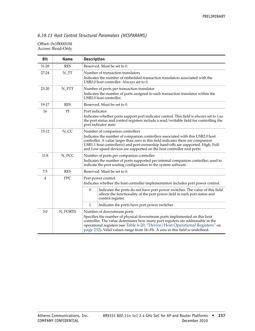
PRELIMINARY
6.19.13 Host Control Structural Parameters (HCSPARAMS)
Offset: 0x1B000104 Access: Read-Only
Bit Name Description
31:28 RES Reserved. Must be set to 0.
27:24 N_TT Number of transaction translatorsIndicates the number of embedded transaction translators associated with the USB2.0 host controller. Always set to 0.
23:20 N_PTT Number of ports per transaction translatorIndicates the number of ports assigned to each transaction translator within the USB2.0 host controller.
19:17 RES Reserved. Must be set to 0.
16 PI Port indicatorIndicates whether ports support port indicator control. This field is always set to 1,so the port status and control registers include a read/writable field for controlling the port indicator state.
15:12 N_CC Number of companion controllersIndicates the number of companion controllers associated with this USB2.0 host controller. A value larger than zero in this field indicates there are companion USB1.1 host controller(s) and port-ownership hand-offs are supported. High, Full- and Low-speed devices are supported on the host controller root ports.
11:8 N_PCC Number of ports per companion controllerIndicates the number of ports supported per internal companion controller; used to indicate the port routing configuration to the system software.
7:5 RES Reserved. Must be set to 0.
4 PPC Port power controlIndicates whether the host controller implementation includes port power control.
0 Indicates the ports do not have port power switches. The value of this field affects the functionality of the port power field in each port status and control register.
1 Indicates the ports have port power switches
3:0 N_PORTS Number of downstream portsSpecifies the number of physical downstream ports implemented on this host controller. The value determines how many port registers are addressable in the operational registers (see Table 6-20, “Device/Host Operational Registers” on page 232). Valid values range from 1h–Fh. A zero in this field is undefined.
Atheros Communications, Inc. AR9331 802.11n 1x1 2.4 GHz SoC for AP and Router Platforms • 237 COMPANY CONFIDENTIAL December 2010 • 237
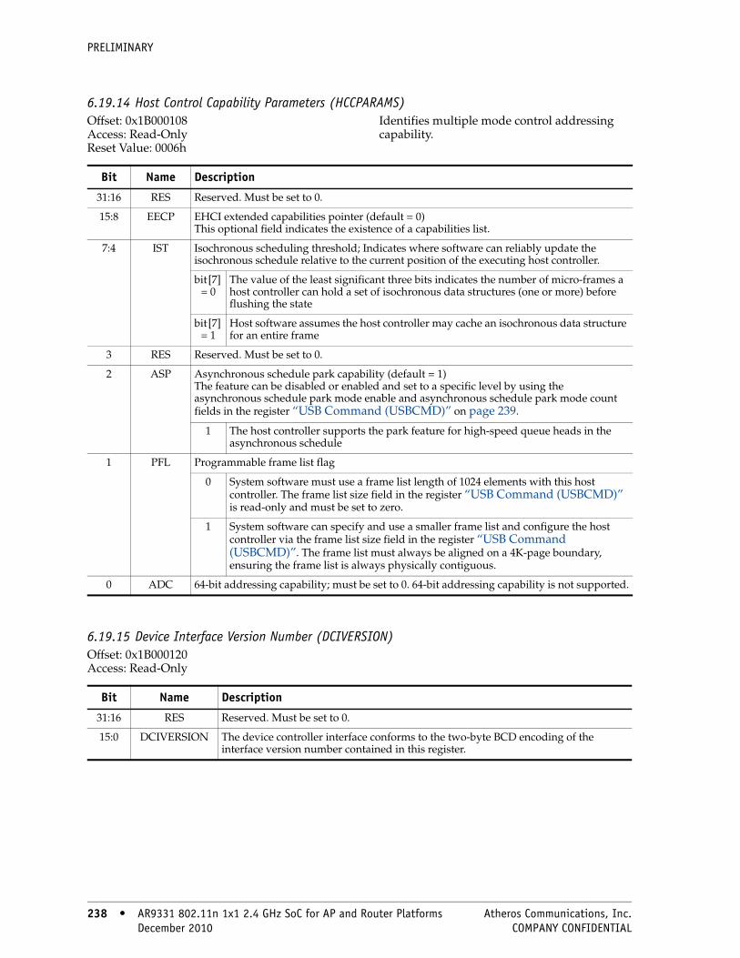
PRELIMINARY
6.19.14 Host Control Capability Parameters (HCCPARAMS)Offset: 0x1B000108 Access: Read-Only Reset Value: 0006h
Identifies multiple mode control addressing capability.
6.19.15 Device Interface Version Number (DCIVERSION)Offset: 0x1B000120 Access: Read-Only
Bit Name Description
31:16 RES Reserved. Must be set to 0.
15:8 EECP EHCI extended capabilities pointer (default = 0) This optional field indicates the existence of a capabilities list.
7:4 IST Isochronous scheduling threshold; Indicates where software can reliably update the isochronous schedule relative to the current position of the executing host controller.
bit [7] = 0
The value of the least significant three bits indicates the number of micro-frames a host controller can hold a set of isochronous data structures (one or more) before flushing the state
bit [7] = 1
Host software assumes the host controller may cache an isochronous data structure for an entire frame
3 RES Reserved. Must be set to 0.
2 ASP Asynchronous schedule park capability (default = 1) The feature can be disabled or enabled and set to a specific level by using the asynchronous schedule park mode enable and asynchronous schedule park mode count fields in the register “USB Command (USBCMD)” on page 239.
1 The host controller supports the park feature for high-speed queue heads in the asynchronous schedule
1 PFL Programmable frame list flag
0 System software must use a frame list length of 1024 elements with this host controller. The frame list size field in the register “USB Command (USBCMD)” is read-only and must be set to zero.
1 System software can specify and use a smaller frame list and configure the host controller via the frame list size field in the register “USB Command (USBCMD)”. The frame list must always be aligned on a 4K-page boundary, ensuring the frame list is always physically contiguous.
0 ADC 64-bit addressing capability; must be set to 0. 64-bit addressing capability is not supported.
Bit Name Description
31:16 RES Reserved. Must be set to 0.
15:0 DCIVERSION The device controller interface conforms to the two-byte BCD encoding of the interface version number contained in this register.
238 • AR9331 802.11n 1x1 2.4 GHz SoC for AP and Router Platforms Atheros Communications, Inc. 238 • December 2010 COMPANY CONFIDENTIAL

PRELIMINARY
6.19.16 Device Control Capability Parameters (DCCPARAMS)Offset: 0x1B000122 Access: Read-Only
6.19.17 USB Command (USBCMD)
Offset: 0x1B000140 Access: See Field Descriptions Reset Value: 00080B00h (host mode) 00080000h (device mode)
Bit Name Description
31:9 RES Reserved. Must be set to 0.
8 HC Host capable; the controller can operate as an EHCI-compatible USB 2.0 host controller.
7 DC Device capable; when set to 1, this controller is capable of operating as a USB 2.0 device.
6:5 RES Reserved. Must be set to 0.
4:0 DEN Device endpoint number Indicates the number of endpoints (0–16) built into the device controller. If this controller is not device capable, this field is zero.
Bit Name Description
31:24 RES Reserved. Must be set to zero.
23:16 ITC RW Interrupt threshold control System software uses this field to set the max. rate the host/device controller issues interrupts at. ITC contains the maximum interrupt interval measured in micro-frames.
00h Immediate (no threshold)
01h 1 micro-frame
02h 2 micro-frames
04h 4 micro-frames
08h 8 micro-frames
10h 16 micro-frames
20h 32 micro-frames
40h 64 micro-frames
Atheros Communications, Inc. AR9331 802.11n 1x1 2.4 GHz SoC for AP and Router Platforms • 239 COMPANY CONFIDENTIAL December 2010 • 239
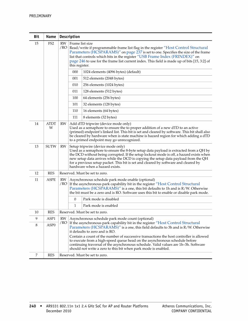
PRELIMINARY
15 FS2 RW/RO
Frame list size Read/write if programmable frame list flag in the register “Host Control Structural Parameters (HCSPARAMS)” on page 237 is set to one. Specifies the size of the frame list that controls which bits in the register “USB Frame Index (FRINDEX)” on page 246 to use for the frame list current index. This field is made up of bits [15, 3:2] of this register.
000 1024 elements (4096 bytes) (default)
001 512 elements (2048 bytes)
010 256 elements (1024 bytes)
011 128 elements (512 bytes)
100 64 elements (256 bytes)
101 32 elements (128 bytes)
110 16 elements (64 bytes)
111 8 elements (32 bytes)
14 ATDTW
RW Add dTD tripwire (device mode only) Used as a semaphore to ensure the to proper addition of a new dTD to an active (primed) endpoint’s linked list. This bit is set and cleared by software. This bit shall also be cleared by hardware when is state machine is hazard region for which adding a dTD to a primed endpoint may go unrecognized.
13 SUTW RW Setup tripwire (device mode only) Used as a semaphore to ensure the 8-byte setup data payload is extracted from a QH by the DCD without being corrupted. If the setup lockout mode is off, a hazard exists when new setup data arrives while the DCD is copying the setup data payload from the QH for a previous setup packet. This bit is set and cleared by software and cleared by hardware when a hazard exists.
12 RES Reserved. Must be set to zero.
11 ASPE RW/RO
Asynchronous schedule park mode enable (optional) If the asynchronous park capability bit in the register “Host Control Structural Parameters (HCSPARAMS)” is a one, this bit defaults to 1h and is R/W. Otherwise the bit must be a zero and is RO. Software uses this bit to enable or disable park mode.
0 Park mode is disabled
1 Park mode is enabled
10 RES Reserved. Must be set to zero.
9 ASP1 RW/RO
Asynchronous schedule park mode count (optional) If the asynchronous park capability bit in the register “Host Control Structural Parameters (HCSPARAMS)” is a one, this field defaults to 3h and is R/W. Otherwise it defaults to zero and is RO. Contain a count of the number of successive transactions the host controller is allowed to execute from a high-speed queue head on the asynchronous schedule before continuing traversal of the asynchronous schedule. Valid values are 1h–3h. Software should not write a zero to this bit when park mode is enabled.
8 ASP0
7 RES Reserved. Must be set to zero.
Bit Name Description
240 • AR9331 802.11n 1x1 2.4 GHz SoC for AP and Router Platforms Atheros Communications, Inc. 240 • December 2010 COMPANY CONFIDENTIAL

PRELIMINARY
6 IAA RW Interrupt on asynchronous advance doorbell (host mode only) Used as a doorbell by software to tell the host controller to issue an interrupt the next time it advances asynchronous schedule. Software must write a 1 to this bit to ring the doorbell. When the host controller has evicted all appropriate cached schedule states, it sets the interrupt on the asynchronous advance status bit in the register “USB Status (USBSTS)”. If the interrupt on synchronous advance enable bit in the register “USB Interrupt Enable (USBINTR)” is set to one, the host controller asserts an interrupt at the next interrupt threshold.The host controller sets this bit to zero after setting the interrupt on the synchronous advance status bit in the register “USB Status (USBSTS)” to one. Software should not write a one to this bit if asynchronous schedule is inactive.
5 ASE RW Asynchronous schedule enable (host mode only)
0 Do not process the asynchronous schedule (default)
1 Use the register “Next Asynchronous List Address (ASYNCLISTADDR)” to access the asynchronous schedule
4 PSE RW Periodic schedule enable (host mode only)
0 Do not process the periodic schedule (default)
1 Use the register “Frame List Base Address (PERIODICLISTBASE)” on page 247 to access the asynchronous schedule
3 FS1 RW/RO
Frame list size See bit [15], “FS2”, for description.2 FS0
1 RST RW Controller reset (RESET) Software uses this bit to reset the controller. This bit is set to zero by the host/device controller when the reset process is complete. Software cannot terminate the reset process early by writing a zero to this register.
Host When this bit is enabled, the host controller resets internal pipelines, timers, etc. to the initial values. Any transaction in progress on USB is immediately terminated. A USB reset is not driven on downstream ports. SW should not set this bit to 1 when HCHalted in the register “USB Status (USBSTS)” is set to 0.
Device When software writes a 1 to this bit, the device controller resets internal pipelines, timers, etc. to the initial values. Writing a 1 to this bit when the device is in the attached state is not recommended. To ensure the device is not in attached state before initiating a device controller reset, primed endpoints must be flushed and the run/stop bit [0] set to 0.
0 RS RW Run/Stop (1 = Run, 0 = stop (default))
Host When set to a 1, the host controller proceeds with the schedule and continues as long as this bit is set to 1. When this bit is set to 0, the host controller completes the current transaction on the USB then halts. The HCHalted bit in the register “USB Status (USBSTS)” indicates when the host controller has completed the transaction and stopped. Software should not write a one to this field unless the host controller is stopped.
Device Writing a 1 to this bit causes the device controller to enable a pull-up on D+ and initiates an attach event. This bit is not connected to pull-up enable, as the pull-up becomes disabled on transitioning to high-speed mode. This bit to prevents an attach event before the device controller is properly initialized. Writing a 0 causes a detach event.
Bit Name Description
Atheros Communications, Inc. AR9331 802.11n 1x1 2.4 GHz SoC for AP and Router Platforms • 241 COMPANY CONFIDENTIAL December 2010 • 241
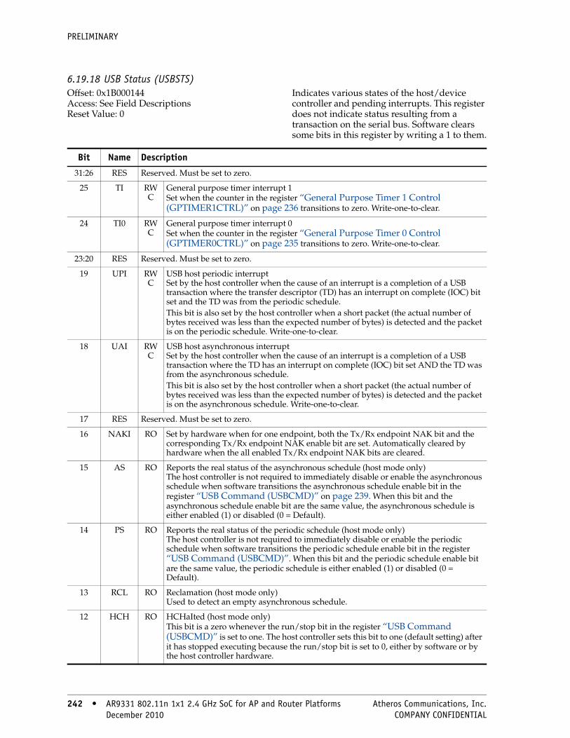
PRELIMINARY
6.19.18 USB Status (USBSTS)Offset: 0x1B000144 Access: See Field Descriptions Reset Value: 0
Indicates various states of the host/device controller and pending interrupts. This register does not indicate status resulting from a transaction on the serial bus. Software clears some bits in this register by writing a 1 to them.
Bit Name Description
31:26 RES Reserved. Must be set to zero.
25 TI RWC
General purpose timer interrupt 1 Set when the counter in the register “General Purpose Timer 1 Control (GPTIMER1CTRL)” on page 236 transitions to zero. Write-one-to-clear.
24 TI0 RWC
General purpose timer interrupt 0 Set when the counter in the register “General Purpose Timer 0 Control (GPTIMER0CTRL)” on page 235 transitions to zero. Write-one-to-clear.
23:20 RES Reserved. Must be set to zero.
19 UPI RWC
USB host periodic interrupt Set by the host controller when the cause of an interrupt is a completion of a USB transaction where the transfer descriptor (TD) has an interrupt on complete (IOC) bit set and the TD was from the periodic schedule. This bit is also set by the host controller when a short packet (the actual number of bytes received was less than the expected number of bytes) is detected and the packet is on the periodic schedule. Write-one-to-clear.
18 UAI RWC
USB host asynchronous interrupt Set by the host controller when the cause of an interrupt is a completion of a USB transaction where the TD has an interrupt on complete (IOC) bit set AND the TD was from the asynchronous schedule.This bit is also set by the host controller when a short packet (the actual number of bytes received was less than the expected number of bytes) is detected and the packet is on the asynchronous schedule. Write-one-to-clear.
17 RES Reserved. Must be set to zero.
16 NAKI RO Set by hardware when for one endpoint, both the Tx/Rx endpoint NAK bit and the corresponding Tx/Rx endpoint NAK enable bit are set. Automatically cleared by hardware when the all enabled Tx/Rx endpoint NAK bits are cleared.
15 AS RO Reports the real status of the asynchronous schedule (host mode only) The host controller is not required to immediately disable or enable the asynchronous schedule when software transitions the asynchronous schedule enable bit in the register “USB Command (USBCMD)” on page 239. When this bit and the asynchronous schedule enable bit are the same value, the asynchronous schedule is either enabled (1) or disabled (0 = Default).
14 PS RO Reports the real status of the periodic schedule (host mode only) The host controller is not required to immediately disable or enable the periodic schedule when software transitions the periodic schedule enable bit in the register “USB Command (USBCMD)”. When this bit and the periodic schedule enable bit are the same value, the periodic schedule is either enabled (1) or disabled (0 = Default).
13 RCL RO Reclamation (host mode only) Used to detect an empty asynchronous schedule.
12 HCH RO HCHaIted (host mode only) This bit is a zero whenever the run/stop bit in the register “USB Command (USBCMD)” is set to one. The host controller sets this bit to one (default setting) after it has stopped executing because the run/stop bit is set to 0, either by software or by the host controller hardware.
242 • AR9331 802.11n 1x1 2.4 GHz SoC for AP and Router Platforms Atheros Communications, Inc. 242 • December 2010 COMPANY CONFIDENTIAL

PRELIMINARY
11 RES Reserved. Must be set to zero.
10 ULPII RWC
ULPI interrupt Only present in designs where the configuration constant VUSB_HS_PHY_ULPI = 1.
9 RES Reserved. Must be set to zero.
8 SLI RWC
DCSuspend When a device controller enters a suspend state from an active state, this bit is set to 1. Cleared by the device controller upon exiting from a suspend state. Write-one-to-clear.
7 SRI RWC
Start-of-(micro-)frame (SOF) received When the device controller detects a SOF, this bit is set to 1. When a SOF is late, the device controller automatically sets this bit to indicate that an SOF was expected, thus this bit is set about every 1 ms in device FS mode and every 125 ms in HS mode, and synchronized to the received SOF. Because the device controller initializes to FS before connect, this bit is set at an interval of 1 ms during the prelude to connect and chirp. Write-one-to-clear.
6 URI RWC
USB reset received (device controller only) When the device controller detects a USB Reset and enters the default state (0), this bit is set to 1. Write-one-to-clear.
5 AAI RWC
Interrupt on asynchronous advance System software can force the host controller to issue an interrupt the next time the host controller advances the asynchronous schedule by writing a 1 to the interrupt on asynchronous advance doorbell bit in the register “USB Command (USBCMD)”. Indicates the assertion of that interrupt source. Write-one-to-clear.
4 RES Reserved. Must be set to zero.
3 FRI RWC
Frame list rollover The host controller sets this bit to a 1 when the frame list index rolls over from its maximum value to 0. The exact value at which the rollover occurs depends on frame list size, e.g, if the size (as programmed in the frame list size field of the register “USB Command (USBCMD)”) is 1024, the frame index register rolls over every time FRINDEX [13] toggles. Similarly, if the size is 512, the host controller sets this bit to 1 every time FHINDEX [12] toggles. Write-one-to-clear.
2 PCI RWC
Port change detect
Host The host controller sets this bit to 1 when on any port, a connect status or a port enable/disable change occurs, or the force port resume bit is set as the result of a transition on the suspended port.
Device The device controller sets this bit to1 when the port controller enters full- or high-speed operational state. When the port controller exits full- or high-speed operation states due to reset or suspend events, the notification mechanisms are the USB Reset Received bit and the DCSuspend bits respectively. Write-one-to-clear.
1 UEI RWC
USB error interrupt When completion of a USB transaction results in an error condition, this bit along with the USBINT bit is set by the host/device controller if the TD on which the error interrupt occurred also had its interrupt on complete (IOC) bit set. Write-one-to-clear.
0 UI RWC
USB interrupt Set by the host/device controller when the cause of an interrupt is a completion of a USB transaction where the TD has an interrupt on complete (IOC) bit set.Also set by the host/device controller when a short packet (the actual number of bytes received was less than the expected number of bytes) is detected. Write-one-to-clear.
Bit Name Description
Atheros Communications, Inc. AR9331 802.11n 1x1 2.4 GHz SoC for AP and Router Platforms • 243 COMPANY CONFIDENTIAL December 2010 • 243
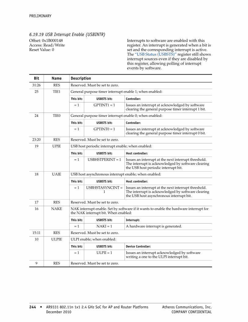
PRELIMINARY
6.19.19 USB Interrupt Enable (USBINTR)Offset: 0x1B000148 Access: Read/Write Reset Value: 0
Interrupts to software are enabled with this register. An interrupt is generated when a bit is set and the corresponding interrupt is active. The “USB Status (USBSTS)” register still shows interrupt sources even if they are disabled by this register, allowing polling of interrupt events by software.
Bit Name Description
31:26 RES Reserved. Must be set to zero.
25 TIE1 General purpose timer interrupt enable 1; when enabled:
This bit: USBSTS bit: Controller:
= 1 GPTINT1 = 1 Issues an interrupt at acknowledged by software clearing the general purpose timer interrupt 1 bit.
24 TIE0 General purpose timer interrupt enable 0; when enabled:
This bit: USBSTS bit: Controller:
= 1 GPTINT0 = 1 Issues an interrupt at acknowledged by software clearing the general purpose timer interrupt 0 bit.
23:20 RES Reserved. Must be set to zero.
19 UPIE USB host periodic interrupt enable; when enabled:
This bit: USBSTS bit: Host controller:
= 1 USBHSTPERINT = 1 Issues an interrupt at the next interrupt threshold. The interrupt is acknowledged by software clearing the USB host periodic interrupt bit.
18 UAIE USB host asynchronous interrupt enable; when enabled:
This bit: USBSTS bit: Host controller:
= 1 USBHSTASYNCINT = 1
Issues an interrupt at the next interrupt threshold. The interrupt is acknowledged by software clearing the USB host asynchronous interrupt bit.
17 RES Reserved. Must be set to zero.
16 NAKE NAK interrupt enable. Set by software if it wants to enable the hardware interrupt for the NAK interrupt bit. When enabled:
This bit: USBSTS bit: Interrupt:
= 1 NAKI = 1 A hardware interrupt is generated.
15:11 RES Reserved. Must be set to zero.
10 ULPIE ULPI enable; when enabled:
This bit: USBSTS bit: Device Controller:
= 1 ULPII = 1 Issues an interrupt acknowledged by software writing a one to the ULPI interrupt bit.
9 RES Reserved. Must be set to zero.
244 • AR9331 802.11n 1x1 2.4 GHz SoC for AP and Router Platforms Atheros Communications, Inc. 244 • December 2010 COMPANY CONFIDENTIAL

PRELIMINARY
8 SLE Sleep enable; when enabled: When this bit is 1, and the bit in the register “USB Status (USBSTS)” transitions, the device controller issues an interrupt acknowledged by software DCSuspend bit.
This bit: USBSTS bit: Device Controller:
= 1 SLI = 1 Issues an interrupt acknowledged by software writing a one to the DCSuspend bit.
7 SRE SOF received enable; when enabled:
This bit: USBSTS bit: Device Controller:
= 1 SRI = 1 Issues an interrupt acknowledged by software clearing the interrupt on the SOF received bit.
6 URE USB reset enable; when enabled:
This bit: USBSTS bit: Device Controller:
= 1 URI = 1 Issues an interrupt acknowledged by software clearing USB reset received bit.
5 AAE Interrupt on asynchronous advance enable; when enabled:
This bit: USBSTS bit: Host/Device Controller:
= 1 AAI = 1 Issues an interrupt acknowledged by software clearing the interrupt on the asynchronous advance bit.
4 SEE System error enable; when enabled:
This bit: USBSTS bit: Host/Device Controller:
= 1 SEI = 1 Issues an interrupt acknowledged by software clearing the system error bit.
3 FRE Frame list rollover enable (host controller only); when enabled:
This bit: USBSTS bit: Host Controller:
= 1 FRI = 1 Issues an interrupt acknowledged by software clearing the frame list rollover bit.
2 PCE Port change detect enable; when enabled:
This bit: USBSTS bit: Host/Device Controller:
= 1 PCE = 1 Issues an interrupt acknowledged by software clearing the port change detect bit.
1 UEE USB error interrupt enable; when enabled:
This bit: USBSTS bit: Host Controller:
= 1 USBERRINT = 1 Issues an interrupt at the next interrupt threshold. The interrupt is acknowledged by software clearing the USB error interrupt bit.
0 UE USB interrupt enable; when enabled:
This bit: USBSTS bit: Host/Device Controller:
= 1 USBINT = 1 Issues an interrupt at the next interrupt threshold. The interrupt is acknowledged by software clearing the USB interrupt bit.
Bit Name Description
Atheros Communications, Inc. AR9331 802.11n 1x1 2.4 GHz SoC for AP and Router Platforms • 245 COMPANY CONFIDENTIAL December 2010 • 245
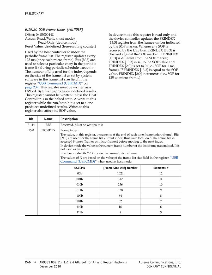
PRELIMINARY
6.19.20 USB Frame Index (FRINDEX)Offset: 0x1B00014C Access: Read/Write (host mode) Read-Only (device mode) Reset Value: Undefined (free-running counter)
Used by the host controller to index the periodic frame list. The register updates every 125 ms (once each micro-frame). Bits [N:3] are used to select a particular entry in the periodic frame list during periodic schedule execution. The number of bits used for the index depends on the size of the frame list as set by system software in the frame list size field in the register “USB Command (USBCMD)” on page 239. This register must be written as a DWord. Byte writes produce-undefined results. This register cannot be written unless the Host Controller is in the halted state. A write to this register while the run/stop hit is set to a one produces undefined results. Writes to this register also affect the SOF value.
In device mode this register is read only and, the device controller updates the FRINDEX [13:3] register from the frame number indicated by the SOF marker. Whenever a SOF is received by the USB bus, FRINDEX [13:3] is checked against the SOF marker. If FRINDEX [13:3] is different from the SOF marker, FRINDEX [13:3] is set to the SOF value and FRINDEX [2:0] is set to 0 (i.e., SOF for 1 ms frame). If FRINDEX [13:3] is equal to the SOF value, FRINDEX [2:0] increments (i.e., SOF for 125-μs micro-frame.)
Bit Name Description
31:14 RES Reserved. Must be written to 0.
13:0 FRINDEX Frame indexThe value, in this register, increments at the end of each time frame (micro-frame). Bits [N:3] are used for the frame list current index, thus each location of the frame list is accessed 8 times (frames or micro-frames) before moving to the next index. In device mode the value is the current frame number of the last frame transmitted. It is not used as an index.In either mode bits 2:0 indicate the current micro-frame.The values of N are based on the value of the frame list size field in the register “USB Command (USBCMD)” when used in host mode:
USBCMD [Frame Size List] Number Elements N
00b 1024 12
001b 512 11
010b 256 10
011b 128 9
100b 64 8
101b 32 7
110b 16 6
111b 8 5
246 • AR9331 802.11n 1x1 2.4 GHz SoC for AP and Router Platforms Atheros Communications, Inc. 246 • December 2010 COMPANY CONFIDENTIAL

PRELIMINARY
6.19.21 Frame List Base Address (PERIODICLISTBASE)Offset: 0x1B000154 Access: Read/Write (writes must be DWord) Reset Value: 0
6.19.22 USB Device Address (DEVICEADDR)Access: Read/Write Reset Value: 0
6.19.23 Next Asynchronous List Address (ASYNCLISTADDR)Offset: 0x1B000158 Access: Read/Write (writes must be DWord) Reset Value: 0
Bit Name Description
31:12 PERBASE Contains the beginning address of the periodic frame list in the system memory. HCD loads this register prior to starting the schedule execution by the host controller. The memory structure referenced by this physical memory pointer is assumed to be 4-Kb aligned. The contents of this register are combined with the frame index register (FRINDEX) to enable the host controller to step through the periodic frame list in sequence.
11:0 RES Reserved. Must be written to zero.
Bit Name Description31:25 USBADR USB device address
After any controller reset or a USB reset, the device address is set to the default address (0). The default address will match all incoming addresses. Software shall reprogram the address after receiving a SET_ADDRESS descriptor.
24 USBADRA Device address advance (default=0)When written to 0, any writes to USBADR are instantaneous.When this bit is written to 1 at the same time or before USBADR (bits [31:25]) is written, the write to the USBADR field is staged and held in a hidden register. After an IN occurs on endpoint 0 and is ACKed, USBADR is loaded from the holding register.Hardware will automatically clear this bit if:■ IN is ACKed to endpoint 0 (USBADR is updated from staging register)■ OUT/SETUP occur to endpoint 0 (USBADR is not updated)■ Device reset occurs (USBADR is reset to 0)Note: After the status phase of the SET_ADDRESS descriptor, the DCD has 2 ms to program the USBADR field. This mechanism ensures this specification is met when the DCD can not write of the device address within 2ms from the SET_ADDRESS status phase. If the DCD writes the USBADR with USBADRA = 1 after the SET_ADDRESS data phase (before the prime of the status phase), the USBADR is programmed instantly at the correct time and meets the 2 ms USB requirement.
23:0 RES Reserved. Must be written to zero.
Bit Name Description31:5 ASYBASE Link pointer low (LPL) (host controller only)
Correspond to memory address signals [31:5], respectively. 4:0 RES Reserved. Must be written to zero.
Atheros Communications, Inc. AR9331 802.11n 1x1 2.4 GHz SoC for AP and Router Platforms • 247 COMPANY CONFIDENTIAL December 2010 • 247
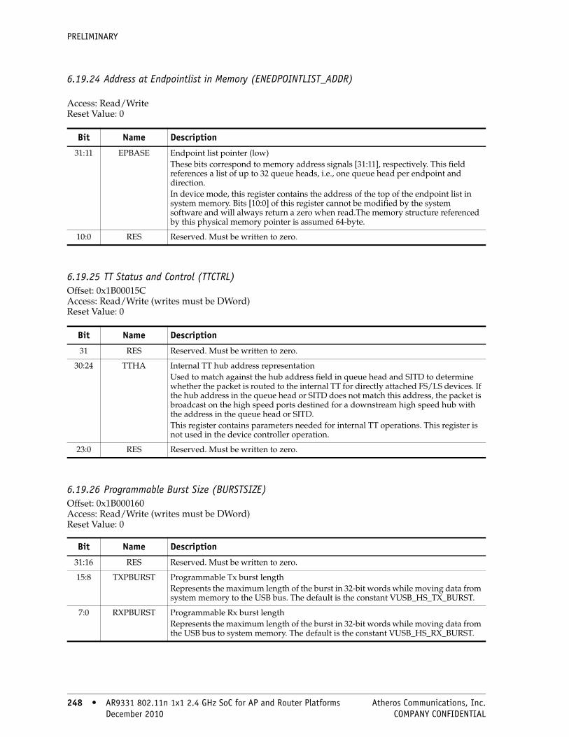
PRELIMINARY
6.19.24 Address at Endpointlist in Memory (ENEDPOINTLIST_ADDR) Access: Read/Write Reset Value: 0
6.19.25 TT Status and Control (TTCTRL)Offset: 0x1B00015C Access: Read/Write (writes must be DWord) Reset Value: 0
6.19.26 Programmable Burst Size (BURSTSIZE)Offset: 0x1B000160 Access: Read/Write (writes must be DWord) Reset Value: 0
Bit Name Description
31:11 EPBASE Endpoint list pointer (low)These bits correspond to memory address signals [31:11], respectively. This field references a list of up to 32 queue heads, i.e., one queue head per endpoint and direction.In device mode, this register contains the address of the top of the endpoint list in system memory. Bits [10:0] of this register cannot be modified by the system software and will always return a zero when read.The memory structure referenced by this physical memory pointer is assumed 64-byte.
10:0 RES Reserved. Must be written to zero.
Bit Name Description
31 RES Reserved. Must be written to zero.
30:24 TTHA Internal TT hub address representationUsed to match against the hub address field in queue head and SITD to determine whether the packet is routed to the internal TT for directly attached FS/LS devices. If the hub address in the queue head or SITD does not match this address, the packet is broadcast on the high speed ports destined for a downstream high speed hub with the address in the queue head or SITD.This register contains parameters needed for internal TT operations. This register is not used in the device controller operation.
23:0 RES Reserved. Must be written to zero.
Bit Name Description
31:16 RES Reserved. Must be written to zero.
15:8 TXPBURST Programmable Tx burst lengthRepresents the maximum length of the burst in 32-bit words while moving data from system memory to the USB bus. The default is the constant VUSB_HS_TX_BURST.
7:0 RXPBURST Programmable Rx burst lengthRepresents the maximum length of the burst in 32-bit words while moving data from the USB bus to system memory. The default is the constant VUSB_HS_RX_BURST.
248 • AR9331 802.11n 1x1 2.4 GHz SoC for AP and Router Platforms Atheros Communications, Inc. 248 • December 2010 COMPANY CONFIDENTIAL
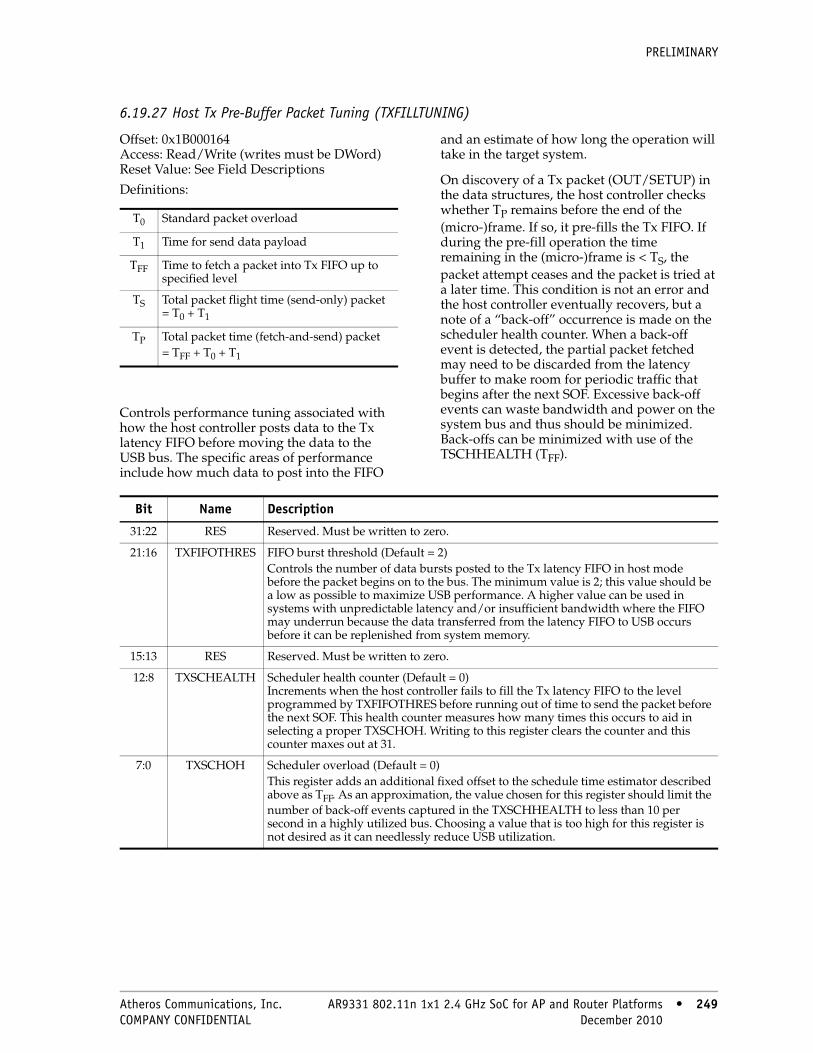
PRELIMINARY
6.19.27 Host Tx Pre-Buffer Packet Tuning (TXFILLTUNING)
Offset: 0x1B000164 Access: Read/Write (writes must be DWord) Reset Value: See Field Descriptions
Definitions:
Controls performance tuning associated with how the host controller posts data to the Tx latency FIFO before moving the data to the USB bus. The specific areas of performance include how much data to post into the FIFO
and an estimate of how long the operation will take in the target system.
On discovery of a Tx packet (OUT/SETUP) in the data structures, the host controller checks whether TP remains before the end of the (micro-)frame. If so, it pre-fills the Tx FIFO. If during the pre-fill operation the time remaining in the (micro-)frame is < TS, the packet attempt ceases and the packet is tried at a later time. This condition is not an error and the host controller eventually recovers, but a note of a “back-off” occurrence is made on the scheduler health counter. When a back-off event is detected, the partial packet fetched may need to be discarded from the latency buffer to make room for periodic traffic that begins after the next SOF. Excessive back-off events can waste bandwidth and power on the system bus and thus should be minimized. Back-offs can be minimized with use of the TSCHHEALTH (TFF).
T0 Standard packet overload
T1 Time for send data payload
TFF Time to fetch a packet into Tx FIFO up to specified level
TS Total packet flight time (send-only) packet = T0 + T1
TP Total packet time (fetch-and-send) packet= TFF + T0 + T1
Bit Name Description
31:22 RES Reserved. Must be written to zero.
21:16 TXFIFOTHRES FIFO burst threshold (Default = 2)Controls the number of data bursts posted to the Tx latency FIFO in host mode before the packet begins on to the bus. The minimum value is 2; this value should be a low as possible to maximize USB performance. A higher value can be used in systems with unpredictable latency and/or insufficient bandwidth where the FIFO may underrun because the data transferred from the latency FIFO to USB occurs before it can be replenished from system memory.
15:13 RES Reserved. Must be written to zero.
12:8 TXSCHEALTH Scheduler health counter (Default = 0) Increments when the host controller fails to fill the Tx latency FIFO to the level programmed by TXFIFOTHRES before running out of time to send the packet before the next SOF. This health counter measures how many times this occurs to aid in selecting a proper TXSCHOH. Writing to this register clears the counter and this counter maxes out at 31.
7:0 TXSCHOH Scheduler overload (Default = 0)This register adds an additional fixed offset to the schedule time estimator described above as TFF. As an approximation, the value chosen for this register should limit the number of back-off events captured in the TXSCHHEALTH to less than 10 per second in a highly utilized bus. Choosing a value that is too high for this register is not desired as it can needlessly reduce USB utilization.
Atheros Communications, Inc. AR9331 802.11n 1x1 2.4 GHz SoC for AP and Router Platforms • 249 COMPANY CONFIDENTIAL December 2010 • 249

PRELIMINARY
6.19.28 Endpoint NAK (ENDPTNAK)Offset: 0x1B000174 Access: Read/Write-to-Clear Reset Value: 0
6.19.29 Endpoint NAK Enable (ENDPTNAKEN)Offset: 0x1B00017C Access: Read/Write Reset Value: 0
Bit Name Description
31:16 EPTN Tx endpoint NAK Each Tx endpoint has 1 bit in this field. The bit is set when the device sends a NAK handshake on a received IN token for the corresponding endpoint.
Bit [15] Endpoint 15
Bit [1] Endpoint 1
Bit [0] Endpoint 0
15:0 EPRN Rx endpoint NAK Each Rx endpoint has 1 bit in this field. The bit is set when the device sends a NAK handshake on a received OUT or PING token for the corresponding endpoint.
Bit [15] Endpoint 15
Bit [1] Endpoint 1
Bit [0] Endpoint 0
Bit Name Description
31:16 EPTNE Tx endpoint NAK enableEach bit is an enable bit for the corresponding Tx endpoint NAK bit. If this bit is set and the corresponding Tx endpoint NAK bit is set, the NAK interrupt bit is set.
Bit [15] Endpoint 15
Bit [1] Endpoint 1
Bit [0] Endpoint 0
15:0 EPRNE Rx endpoint NAK enableEach bit is an enable bit for the corresponding Rx endpoint NAK bit. If this bit is set and the corresponding Rx endpoint NAK bit is set, the NAK interrupt bit is set.
Bit [15] Endpoint 15
Bit [1] Endpoint 1
Bit [0] Endpoint 0
250 • AR9331 802.11n 1x1 2.4 GHz SoC for AP and Router Platforms Atheros Communications, Inc. 250 • December 2010 COMPANY CONFIDENTIAL
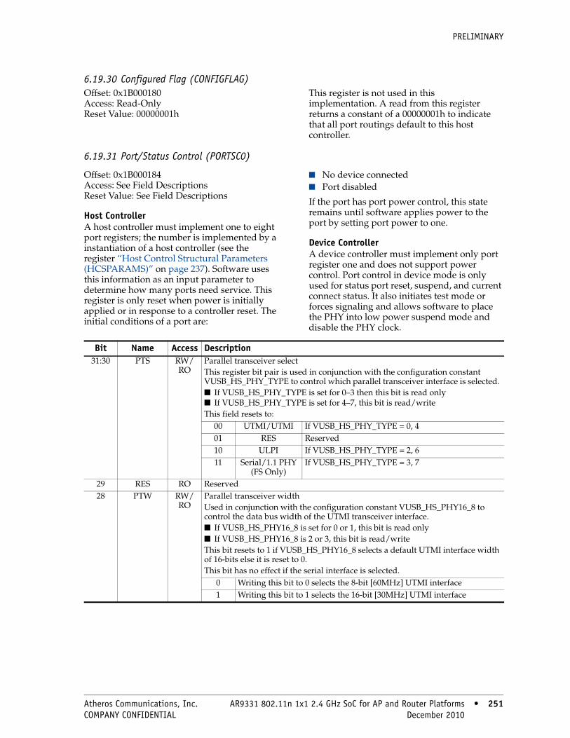
PRELIMINARY
6.19.30 Configured Flag (CONFIGFLAG)Offset: 0x1B000180 Access: Read-Only Reset Value: 00000001h
This register is not used in this implementation. A read from this register returns a constant of a 00000001h to indicate that all port routings default to this host controller.
6.19.31 Port/Status Control (PORTSC0)
Offset: 0x1B000184 Access: See Field Descriptions Reset Value: See Field Descriptions
Host ControllerA host controller must implement one to eight port registers; the number is implemented by a instantiation of a host controller (see the register “Host Control Structural Parameters (HCSPARAMS)” on page 237). Software uses this information as an input parameter to determine how many ports need service. This register is only reset when power is initially applied or in response to a controller reset. The initial conditions of a port are:
■ No device connected■ Port disabled
If the port has port power control, this state remains until software applies power to the port by setting port power to one.
Device ControllerA device controller must implement only port register one and does not support power control. Port control in device mode is only used for status port reset, suspend, and current connect status. It also initiates test mode or forces signaling and allows software to place the PHY into low power suspend mode and disable the PHY clock.
Bit Name Access Description31:30 PTS RW/
ROParallel transceiver select This register bit pair is used in conjunction with the configuration constant VUSB_HS_PHY_TYPE to control which parallel transceiver interface is selected. ■ If VUSB_HS_PHY_TYPE is set for 0–3 then this bit is read only■ If VUSB_HS_PHY_TYPE is set for 4–7, this bit is read/writeThis field resets to:
00 UTMI/UTMI If VUSB_HS_PHY_TYPE = 0, 401 RES Reserved10 ULPI If VUSB_HS_PHY_TYPE = 2, 611 Serial/1.1 PHY
(FS Only)If VUSB_HS_PHY_TYPE = 3, 7
29 RES RO Reserved28 PTW RW/
ROParallel transceiver widthUsed in conjunction with the configuration constant VUSB_HS_PHY16_8 to control the data bus width of the UTMI transceiver interface. ■ If VUSB_HS_PHY16_8 is set for 0 or 1, this bit is read only■ If VUSB_HS_PHY16_8 is 2 or 3, this bit is read/writeThis bit resets to 1 if VUSB_HS_PHY16_8 selects a default UTMI interface width of 16-bits else it is reset to 0. This bit has no effect if the serial interface is selected.
0 Writing this bit to 0 selects the 8-bit [60MHz] UTMI interface1 Writing this bit to 1 selects the 16-bit [30MHz] UTMI interface
Atheros Communications, Inc. AR9331 802.11n 1x1 2.4 GHz SoC for AP and Router Platforms • 251 COMPANY CONFIDENTIAL December 2010 • 251

PRELIMINARY
27:26 PSPD RO Port speedIndicates the speed at which the port is operating. For HS mode operation in the host controller and HS/FS operation in the device controller the port routing steers data to the protocol engine. For FS and LS mode operation in the host controller, the port routing steers data to the Protocol Engine with the embedded transaction translator.
00 Full Speed01 Low Speed10 High Speed
25 RES RO Reserved. Must be set to zero.24 PFSC RW Port force full speed connect; default = 0b (debug mode only)
Setting this bit to 1 forces the port to only connect at Full Speed and disables the chirp sequence, allowing the port to identify itself as High Speed (useful for testing FS configurations with a HS host, hub or device).
23 PHCD RW PHY low power suspend: clock disable (PLPSCD)0 Disables the PHY clock (Default)1 Enables the PHY clock
Reading this bit indicates the status of the PHY clock. NOTE: The PHY clock cannot be disabled if it is being used as the system clock.Device Mode
The PHY can be put into Low Power Suspend–Clock Disable when the device is not running (USBCMD Run/Stop=0b) or the host has signaled suspend (PORTSC SUSPEND=1b). Low power suspend clears automatically when the host has signaled resume if using a circuit similar to that in 10. Before forcing a resume from the device, the device controller driver must clear this bit.
Host Mode
The PHY can be put into Low Power Suspend–Clock Disable when the downstream device has been put into suspend mode or when no downstream device is connected. Low power suspend is completely under the control of software.
22 WKOC RW Wake on over-current enable (WKOC_E)0 This field is zero if Port Power (PP) is zero (Default)1 Sensitizes the port to over-current conditions as wake-up events
21 WKDS RW Wake on Disconnect Enable (WKDSCNNT_E)0 This field is zero if Port Power (PP) is zero or in device mode (Default)1 Sensitizes the port to device disconnects as wake-up events
20 WKCN RW Wake on connect enable (WKCNNT_E)0 This field is zero if Port Power (PP) is zero or in device mode (Default)1 Sensitizes the port to device connects as wake-up events
19:14 RES RW Reserved13 PO RO Port owner; default = 0
Port owner hand-off is not implemented in this design, therefore this bit always reads back as 0. System software uses this field to release ownership of the port to a selected host controller (in the event that the attached device is not a high-speed device.
00 This bit unconditionally returns to 0 when the configured bit in the register “Configured Flag (CONFIGFLAG)” on page 251 makes a 0 to 1 transition.
01 This bit unconditionally goes to 1 the configured bit in the register “Configured Flag (CONFIGFLAG)” on page 251 is zero. A one in this bit indicates that an internal companion controller owns and controls the port. Software writes a one to this bit when the attached device is not a high-speed device.
12 RES RW Reserved
Bit Name Access Description
252 • AR9331 802.11n 1x1 2.4 GHz SoC for AP and Router Platforms Atheros Communications, Inc. 252 • December 2010 COMPANY CONFIDENTIAL

PRELIMINARY
11:10 LS RO Line status; bit encoding is:
Setting Meaning00 SE001 J_ STATE10 K_STATE11 Undefined
These bits reflect the current logical levels of the D+ (bit [11]) and D– (bit [10]) signal lines.Device Mode
In device mode, the use of line-state by the device controller driver is not necessary.
Host Mode
In host mode, the use of line-state by the host controller driver is not necessary (unlike EHCI), because the port controller state machine and the port routing manage the connection of LS and FS.
9 HSP RO High-speed port; see also bits [27:26], PSPD0 Connected host/device is not in a high-speed mode (Default)1 The host/device connected to the port is in high-speed mode
8 PR RW/RO
Port reset■ This field is zero if Port power (PP) is zero■ When software writes a one to this bit, the bus-reset sequence as defined in
USB2.0 is started. This bit automatically changes to zero after reset.
Device Mode: Read-OnlyDevice reset from the USB bus is also indicated in the register “USB Status (USBSTS)” on page 242.
Host Mode: Read/Write0 Port is not in reset (Default)1 Port is in reset
7 SUSP RW/RO
Suspend Port Enabled Bit and Suspend bit of this register define the port states:
Bits Port State0x Disable10 Enable11 Suspend
This field is zero if Port Power (PP) is zero in host mode.Device Mode
Read-Only■ 0=Port not in suspend state (Default)■ 1=Port in suspend state
Host Mode
Read/Write■ 0=Port not in suspend state (Default)■ 1=Port in suspend stateIn suspend state, downstream propagation of data is blocked on this port, except for port reset. The blocking occurs at the end of the current transaction if a transaction was in progress when this bit was written to 1. In the suspend state, the port is sensitive to resume detection. Note that the bit status does not change until the port is suspended and that there may be a delay in suspending a port if there is a transaction currently in progress on the USB.The host controller unconditionally sets this bit to zero when software sets the force port resume bit to zero. The host controller ignores a write of zero to this bit. If host software sets this bit to a one when the port is not enabled (i.e. Port enabled bit is a zero) the results are undefined.
Bit Name Access Description
Atheros Communications, Inc. AR9331 802.11n 1x1 2.4 GHz SoC for AP and Router Platforms • 253 COMPANY CONFIDENTIAL December 2010 • 253

PRELIMINARY
6 FPR RW Force port resume0 No resume (K-state) detected/driven on port (Default)1 Resume detected/driven on port
This field is zero if Port Power (PP) is zero in host mode.Device Mode
After the device has been in suspend state for 5 ms or more, software must set this bit to 1 to drive resume signaling before clearing. The device controller sets this bit to one if a J-to-K transition is detected while the port is in the suspend state. The bit will be cleared when the device returns to normal operation. Also, when this bit transitions to a one because a J-to-K transition detected, the port change detect bit in the register“USB Status (USBSTS)” is also set to one.
Host Mode
Software sets this bit to one to drive resume signaling. The host controller sets this bit to one if a J-to-K transition is detected while the port is in the suspend state. When this bit transitions to a one because a J-to-K transition is detected, the port change detect bit in the register “USB Status (USBSTS)” is also set to one. This bit automatically changes to zero after the resume sequence is complete. This behavior is different from EHCI where the host controller driver is required to set this bit to a zero after the resume duration is timed in the driver.
5 OCC RWC Over-current change. For device-only implementations this bit shall always be 0.0 (Default)1 This bit is set to 1 when there is a change to over-current active.
Software clears this bit by writing a one to this bit position.4 OCA RO Over-current active. For device-only implementations this bit shall always be 0.
0 This port does not have an over-current condition. This bit automatically transitions from one to zero when the over-current condition is removed. (Default)
1 This port currently has an over-current condition3 PEC RWC Port enable/disable change
0 No change (Default)1 Port enabled/disabled status has changed
This field is zero if Port Power (PP) is zero.Device Mode
The device port is always enabled (this bit will be zero)
Host Mode
For the root hub, this bit gets set to a one only when a port is disabled due to disconnect on the port or due to the appropriate conditions existing at the EOF2 point (See Chapter 11 of the USB Specification). Software clears this by writing a one to it.
2 PE RW Port enabled/disabled 0 Disabled (Default)1 Enabled
This field is zero if Port Power (PP) is zero in host mode.Device Mode
The device port is always enabled (this bit will be one)
Host Mode
Ports can only be enabled by the host controller as a part of reset and enable. Software cannot enable a port by writing a one to this field. Ports can be disabled by either a fault condition (disconnect event or other fault condition) or by the host software. Note that the bit status does not change until the port state actually changes. There may be a delay in disabling or enabling a port due to other host controller and bus events. When the port is disabled, (0b) downstream propagation of data is blocked except for reset.
Bit Name Access Description
254 • AR9331 802.11n 1x1 2.4 GHz SoC for AP and Router Platforms Atheros Communications, Inc. 254 • December 2010 COMPANY CONFIDENTIAL
PRELIMINARY
6.19.32 USB Mode (USBMODE)Offset: 0x1B0001A8 Access: Read/Write Reset Value: 0
1 CSC RWC Connect status change0 No change (Default)1 Change in current connect status. Software clears this bit by writing a 1
to it.This field is zero if Port Power (PP) is zero in host mode.Device Mode
This bit is undefined in device controller mode.
Host Mode
Indicates a change has occurred in the port’s Current Connect Status. The host/device controller sets this bit for all changes to the port device connect status, even if system software has not cleared an existing connect status change. For example, the insertion status changes twice before system software has cleared the changed condition, hub hardware will be ‘setting’ an already-set bit (i.e., the bit will remain set).
0 CCS RO Current connect statusDevice Mode
■ 0 = Not attached (Default) A zero indicates that the device did not attach successfully or was forcibly disconnected by the software writing a zero to the Run bit in the register “USB Command (USBCMD)” on page 239. It does not state the device being disconnected or suspended.
■ 1 = Attached A 1 indicates that the device successfully attached and is operating in either high speed or full speed as indicated by the high speed port bit in this register.
Host Mode
This value reflects the current state of the port, and may not correspond directly to the event that caused the connect status change bit to be set. ■ 0 = No device is present. (Default)■ 1 = Device is present on port. This field is zero if Port Power (PP) is zero in host mode.
Bit Name Access Description
Bit Name Description
31:5 RES Reserved. Must be written to zero.
4 SDIS Stream disable mode■ 0 = Inactive (Default)■ 1 = Active
Device Mode
Setting to a 1 disables double priming on both Rx and Tx for low bandwidth systems. This mode, when enabled, ensures that the Rx and Tx buffers are sufficient to contain an entire packet, so the usual double buffering scheme is disabled to prevent overruns/underruns in bandwidth limited systems.
Host Mode
Setting to a 1 ensures that overruns/underruns of the latency FIFO are eliminated for low bandwidth systems where the Rx and Tx buffers are sufficient to contain the entire packet. Enabling stream disable also has the effect of ensuring the Tx latency is filled to capacity before the packet is launched onto the USB.
Atheros Communications, Inc. AR9331 802.11n 1x1 2.4 GHz SoC for AP and Router Platforms • 255 COMPANY CONFIDENTIAL December 2010 • 255

PRELIMINARY
6.19.33 Endpoint Setup Status (ENDPTSETUPSTAT)Offset: 0x1B0001AC Access: Read/Write-One-to-Clear Reset Value: 00000000h
3 SLOM Setup lockout mode In device mode, this bit controls behavior of the setup lock mechanism.
0 Setup lockouts on (Default)
1 Setup lockouts off
2 ES Endian selectCan change the byte ordering of transfer buffers to match the host microprocessor bus architecture. The bit fields in the microprocessor interface and the DMA data structures (including the setup buffer within the device QH) are unaffected by the value of this bit, because they are based upon 32-bit words.
Bit Meaning
0 Little Endian (Default)First byte referenced in least significant byte of 32-bit word
1 Big EndianFirst byte referenced in most significant byte of 32-bit word
1:0 CM Controller mode
Bit Meaning
00 Idle (Default for combination host/device)
01 Reserved
10 Device Controller (Default for device-only controller)
11 Host Controller (Default for host-only controller)
Bit Name Description
Bit Name Description
31:16 RES Reserved
15:0 ENDPTSETUPSTAT Setup endpoint statusFor every setup transaction received, a corresponding bit in this register is set to 1. Software must clear or acknowledge the setup transfer by writing a one to a respective bit after it has read the setup data from Queue head. The response to a setup packet as in the order of operations and total response time is crucial to limit bus time outs while the setup lock our mechanism is engaged. See Managing Endpoints in the Device Operational Model.
256 • AR9331 802.11n 1x1 2.4 GHz SoC for AP and Router Platforms Atheros Communications, Inc. 256 • December 2010 COMPANY CONFIDENTIAL

PRELIMINARY
6.19.34 Endpoint Initialization (ENDPTPRIME)Offset: 0x1B0001B0 Access: Read/Write-One-to-Clear Reset Value: 00000000h
6.19.35 Endpoint De-Initialization (ENDPTFLUSH)Offset: 0x1B0001B4Access: Writing a 1 to a bit in this register
causes the associated endpoint(s) to clear any primed buffers.
Reset Value: 0
Bit Name Description
31:16 PETB Prime endpoint Tx bufferFor each endpoint a corresponding bit is used to request that a buffer prepared for a Tx operation in order to respond to a USB IN/INTERRUPT transaction. Software should write a 1 to the corresponding bit when posting a new transfer descriptor to an endpoint. Hardware automatically uses this bit to begin parsing for a new transfer descriptor from the queue head and prepare a Tx buffer. Hardware clears this bit when the associated endpoint(s) are successfully primed.
Bit [15] Endpoint 15
Bit [1] Endpoint 1
Bit [0] Endpoint 0
15:0 PERB Prime endpoint Rx bufferFor each endpoint a corresponding bit is used to request that a buffer prepared for a Rx operation in order to respond to a USB IN/INTERRUPT transaction. Software should write a 1 to the corresponding bit when posting a new transfer descriptor to an endpoint. Hardware automatically uses this bit to begin parsing for a new transfer descriptor from the queue head and prepare a Rx buffer. Hardware clears this bit when the associated endpoint(s) are successfully primed.
Bit [15] Endpoint 15
Bit [1] Endpoint 1
Bit [0] Endpoint 0
Bit Name Description31:16 FETB Flush endpoint Tx buffer
If a packet is in progress for one of the associated endpoints, that transfer continues until completion. Hardware clears this register after the endpoint flush operation.
Bit [15] Endpoint 15
Bit [1] Endpoint 1
Bit [0] Endpoint 0
15:0 FERB Flush endpoint Rx bufferIf a packet is in progress for one of the associated endpoints, that transfer continues until completion. Hardware clears this register after the endpoint flush operation.
Bit [15] Endpoint 15
Bit [1] Endpoint 1
Bit [0] Endpoint 0
Atheros Communications, Inc. AR9331 802.11n 1x1 2.4 GHz SoC for AP and Router Platforms • 257 COMPANY CONFIDENTIAL December 2010 • 257

PRELIMINARY
6.19.36 Endpoint Status (ENDPTSTATUS)Offset: 0x1B0001B8 Access: Read-Only Reset Value: 0
6.19.37 Endpoint Complete (ENDPTCOMPLETE)Offset: 0x1B0001BC Access: Read/Write-One-to-Clear Reset Value: 0
Bit Name Description31:16 ETBR Endpoint Tx buffer ready
One bit for each endpoint indicates status of the respective endpoint buffer. This bit is set to a 1 by the hardware as a response to a command from a corresponding bit in the register “Endpoint Initialization (ENDPTPRIME)” on page 257. A delay always occurs between setting a bit in the ENDPTPRIME register and endpoint indicating ready. This delay time varies based upon the current USB traffic and the number of bits set in the ENDPTPRIME register. Buffer ready is cleared by USB reset, by the USB DMA system, or through the ENDPTFLUSH register.
Bit [15] Endpoint 15
Bit [1] Endpoint 1
Bit [0] Endpoint 0
15:0 ERBR Endpoint Rx buffer readyOne bit for each endpoint indicates status of the respective endpoint buffer. This bit is set to a 1 by the hardware as a response to a command from a corresponding bit in the register “Endpoint Initialization (ENDPTPRIME)”. A delay always occurs between setting a bit in the ENDPTPRIME register and endpoint indicating ready. This delay time varies based upon the current USB traffic and the number of bits set in the ENDPTPRIME register. Buffer ready is cleared by USB reset, by the USB DMA system, or through the ENDPTFLUSH register.
Bit [15] Endpoint 15
Bit [1] Endpoint 1
Bit [0] Endpoint 0
Bit Name Description
31:16 ETCE Endpoint Tx complete eventIndicates a Tx event (IN/INTERRUPT) occurred and software should read the corresponding endpoint queue to determine the endpoint status. If the corresponding IOC bit is set in the transfer descriptor, this bit is set simultaneously with the register USBINTR.
Bit [15] Endpoint 15
Bit [1] Endpoint 1
Bit [0] Endpoint 0
258 • AR9331 802.11n 1x1 2.4 GHz SoC for AP and Router Platforms Atheros Communications, Inc. 258 • December 2010 COMPANY CONFIDENTIAL

PRELIMINARY
6.19.38 Endpoint Control 0 (ENDPTCTRL0)Offset: 0x1B0001C0 Access: Read/Write Reset Value: 0080008h
Every device implements Endpoint0 as a control endpoint.
15:0 ERCE Endpoint Rx complete eventIndicates a Rx event (IN/INTERRUPT) occurred and software should read the corresponding endpoint queue to determine the endpoint status. If the corresponding IOC bit is set in the transfer descriptor, this bit is set simultaneously with the register USBINTR.
Bit [15] Endpoint 15
Bit [1] Endpoint 1
Bit [0] Endpoint 0
Bit Name Description
Bit Name Description31:24 RES Reserved. Must be written to zero.
23 TXE Tx endpoint enable
22:20 RES Reserved. Must be written to zero.
19:18 TXT Tx endpoint type (0 = Control)
17 RES Reserved. Must be written to zero.
16 TXS Tx endpoint stall
0 Endpoint OK (Default)
1 Endpoint stalled
15:8 RES Reserved. Must be written to zero.
7 RXE Rx endpoint enable
6:4 RES Reserved. Must be written to zero.
3:2 RXT Rx endpoint type (0 = Control)
1 RES Reserved. Must be written to zero.
0 RXS Rx endpoint stall
0 Endpoint OK (Default)
1 Endpoint stalled
Atheros Communications, Inc. AR9331 802.11n 1x1 2.4 GHz SoC for AP and Router Platforms • 259 COMPANY CONFIDENTIAL December 2010 • 259

PRELIMINARY
6.19.39 Endpoint Control 1 (ENDPTCTRL1)Offset: 0x1B0001C4 (Endpoint Control 1) 0x1B0001C8 (Endpoint Control 2) 0x1B0001CC (Endpoint Control 3) 0x1B0001D0 (Endpoint Control 4) 0x1B0001D4 (Endpoint Control 5) Access: Read/Write Reset Value: 0
Bit Name Description31:24 RES Reserved. Must be written to zero.
23 TXE Tx endpoint enableAn Endpoint should be enabled only after it has been configured
22 TXR Tx data toggle resetWhen a configuration event is received for this Endpoint, software must write a 1 to this bit in order to synchronize the data PIDs between the host and device.
21 TXI Tx data toggle inhibit
0 PID sequencing enabled (Default)
1 PID sequencing disabled
20 RES Reserved. Must be written to zero.
19:18 TXT Tx endpoint type
00 Control
01 Isochronous
10 Bulk
11 Interrupt
17 TXD Tx endpoint data source; should always be written to zero
16 TXS Tx endpoint stall
0 Endpoint OK (Default)
1 Endpoint stalled
15:8 RES Reserved. Must be written to zero.
7 RXE Rx endpoint enableAn Endpoint should be enabled only after it has been configured
6 RXR Rx data toggle resetWhen a configuration event is received for this Endpoint, software must write a 1 to this bit in order to synchronize the data PIDs between the host and device.
5 RXI Rx data toggle inhibit
0 PID sequencing enabled (Default)
1 PID sequencing disabled
4:3 RES Reserved. Must be written to zero.
2 RXT Tx endpoint type
00 Control
01 Isochronous
10 Bulk
11 Interrupt
1 RXD Rx endpoint data source; should always be written to zero
0 RXS Rx endpoint stall
0 Endpoint OK (Default)
1 Endpoint stalled
260 • AR9331 802.11n 1x1 2.4 GHz SoC for AP and Router Platforms Atheros Communications, Inc. 260 • December 2010 COMPANY CONFIDENTIAL

PRELIMINARY
6.20 Serial Flash RegistersTable 6-21 shows the serial flash registers for the AR9331.
6.20.1 SPI Function Select (SPI_FUNC_SELECT)Address: 0x1F000000 Access: Read/Write Reset: 0x0
Enables or disables the SPI.
6.20.2 SPI Control (SPI_CONTROL)Address: 0x1F000004 Access: Read/Write Reset: See field description
Used to set the functions for the SPI control, and can be written only if the FUNCTION_SELECT bit is set to 1.
6.20.3 SPI I/O Control (SPI_IO_CONTROL)Address: 0x1F000008 Access: Read/Write Reset: 0x0
This register is used to configure the in/out bits for the SPI.
6.20.4 SPI Read Data (SPI_READ_DATA)Address: 0x1F00000C Access: Read-Only Reset: 0x0
Used to return the data read from the flash device with bits sampled after every clock.
Table 6-21. Serial Flash Registers
Offset Name Description Page0x1F000000 SPI_FUNCTION_SELECT SPI Function Select Register page 2610x1F000004 SPI_CONTROL SPI Control Register page 2610x1F000008 SPI_IO_CONTROL SPI IO Control page 2610x1F00000C SPI_READ_DATA SPI Read Data page 261
Bit Bit Name Description31:1 RES Reserved. Must be written with zero. Contains zeros when read.
0 FUNCTION_ SELECT 0 enables SPI. Setting this bit to 1 makes the other registers visible
Bit Bit Name Reset Description31:7 RES 0x0 Reserved. Must be written with zero. Contains zeros when read.
6 REMAP_ DISABLE
0x0 Remaps 4 MB space over unless explicitly disabled by setting this bit to 1. If set to 1, 16 MB is accessible.
5:0 CLOCK_ DIVIDER
0x8 Specifies the clock divider setting. Actual clock frequency would be (AHB_CLK/((CLOCK_DIVIDER+1)*2)). Therefore by default, if the AHB_CLK is 200 MHz, this would give 200/18 = ~11MHz.
Bit Bit Name Description31:19 RES Reserved. Must be written with zero. Contains zeros when read.
18 IO_CS_2 The chip select 2 bit to be output17 IO_CS_1 The chip select 1 bit to be output16 IO_CS_0 The chip select 0 bit to be output8 IO_CLOCK The clock bit to be output
7:1 RES Reserved. Must be written with zero. Contains zeros when read.0 IO_DO The data bit to be output
Bit Bit Name Description31:0 READ_DATA The read data sampled in every clock
Atheros Communications, Inc. AR9331 802.11n 1x1 2.4 GHz SoC for AP and Router Platforms • 261 COMPANY CONFIDENTIAL December 2010 • 261
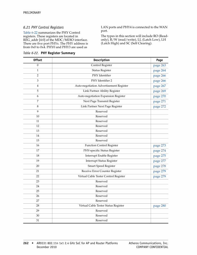
PRELIMINARY
6.21 PHY Control RegistersTable 6-22 summarizes the PHY Control registers. These registers are located in REG_addr [4:0] of the MDC/MDIO interface. There are five port PHYs. The PHY address is from 0x0 to 0x4. PHY0 and PHY3 are used as
LAN ports and PHY4 is connected to the WAN port.
The types in this section will include RO (Read-only), R/W (read/write), LL (Latch Low), LH (Latch High) and SC (Self Clearing).
Table 6-22. PHY Register Summary
Offset Description Page0 Control Register page 263
1 Status Register page 264
2 PHY Identifier page 266
3 PHY Identifier 2 page 266
4 Auto-negotiation Advertisement Register page 267
5 Link Partner Ability Register page 269
6 Auto-negotiation Expansion Register page 270
7 Next Page Transmit Register page 271
8 Link Partner Next Page Register page 272
9 Reserved
10 Reserved
11 Reserved
12 Reserved
13 Reserved
14 Reserved
15 Reserved
16 Function Control Register page 273
17 PHY-specific Status Register page 274
18 Interrupt Enable Register page 275
19 Interrupt Status Register page 277
20 Smart Speed Register page 278
21 Receive Error Counter Register page 279
22 Virtual Cable Tester Control Register page 279
23 Reserved
24 Reserved
25 Reserved
26 Reserved
27 Reserved
28 Virtual Cable Tester Status Register page 280
29 Reserved
30 Reserved
31 Reserved
262 • AR9331 802.11n 1x1 2.4 GHz SoC for AP and Router Platforms Atheros Communications, Inc. 262 • December 2010 COMPANY CONFIDENTIAL
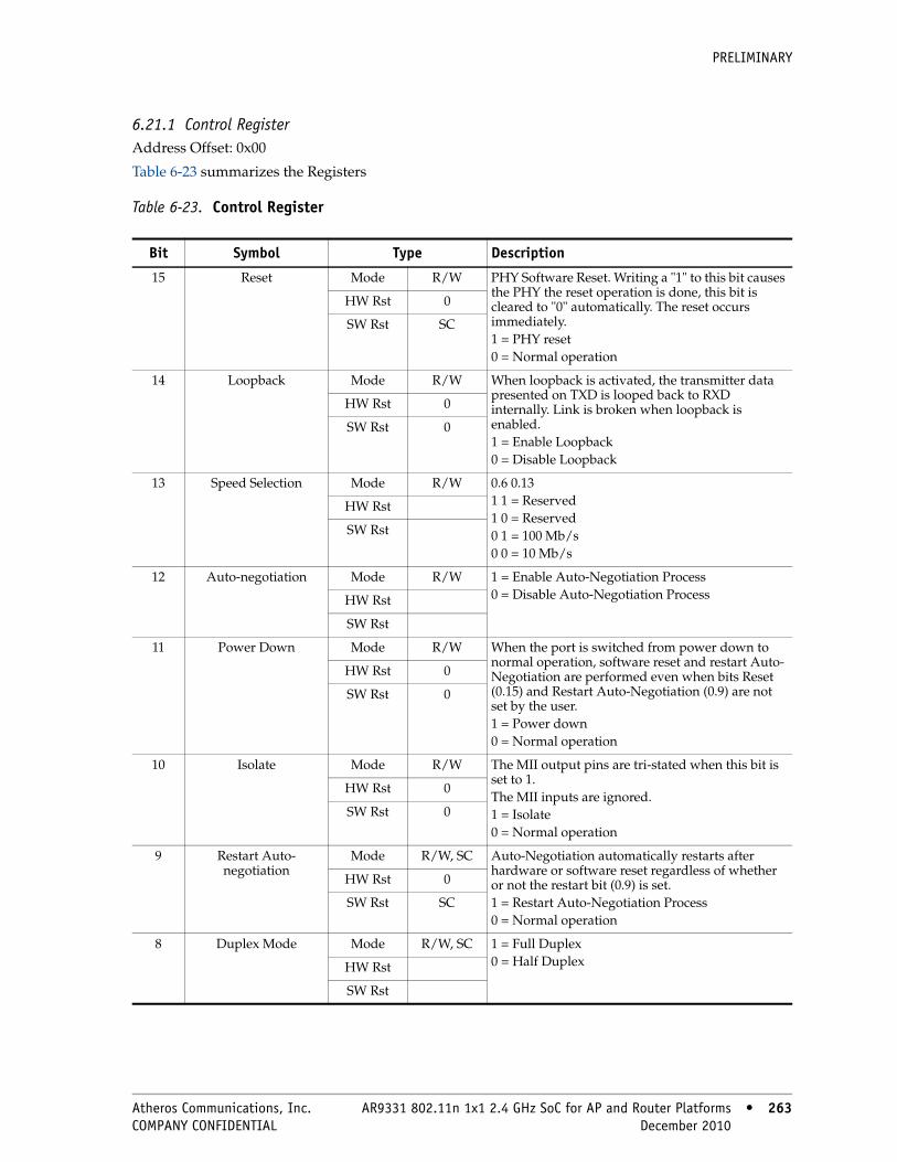
PRELIMINARY
6.21.1 Control RegisterAddress Offset: 0x00
Table 6-23 summarizes the Registers
Table 6-23. Control Register
Bit Symbol Type Description
15 Reset Mode R/W PHY Software Reset. Writing a "1" to this bit causes the PHY the reset operation is done, this bit is cleared to "0" automatically. The reset occurs immediately.1 = PHY reset0 = Normal operation
HW Rst 0
SW Rst SC
14 Loopback Mode R/W When loopback is activated, the transmitter data presented on TXD is looped back to RXD internally. Link is broken when loopback is enabled. 1 = Enable Loopback0 = Disable Loopback
HW Rst 0
SW Rst 0
13 Speed Selection Mode R/W 0.6 0.131 1 = Reserved1 0 = Reserved 0 1 = 100 Mb/s0 0 = 10 Mb/s
HW Rst
SW Rst
12 Auto-negotiation Mode R/W 1 = Enable Auto-Negotiation Process0 = Disable Auto-Negotiation ProcessHW Rst
SW Rst
11 Power Down Mode R/W When the port is switched from power down to normal operation, software reset and restart Auto-Negotiation are performed even when bits Reset (0.15) and Restart Auto-Negotiation (0.9) are not set by the user.1 = Power down0 = Normal operation
HW Rst 0
SW Rst 0
10 Isolate Mode R/W The MII output pins are tri-stated when this bit is set to 1.The MII inputs are ignored.1 = Isolate0 = Normal operation
HW Rst 0
SW Rst 0
9 Restart Auto-negotiation
Mode R/W, SC Auto-Negotiation automatically restarts after hardware or software reset regardless of whether or not the restart bit (0.9) is set.1 = Restart Auto-Negotiation Process0 = Normal operation
HW Rst 0
SW Rst SC
8 Duplex Mode Mode R/W, SC 1 = Full Duplex 0 = Half DuplexHW Rst
SW Rst
Atheros Communications, Inc. AR9331 802.11n 1x1 2.4 GHz SoC for AP and Router Platforms • 263 COMPANY CONFIDENTIAL December 2010 • 263
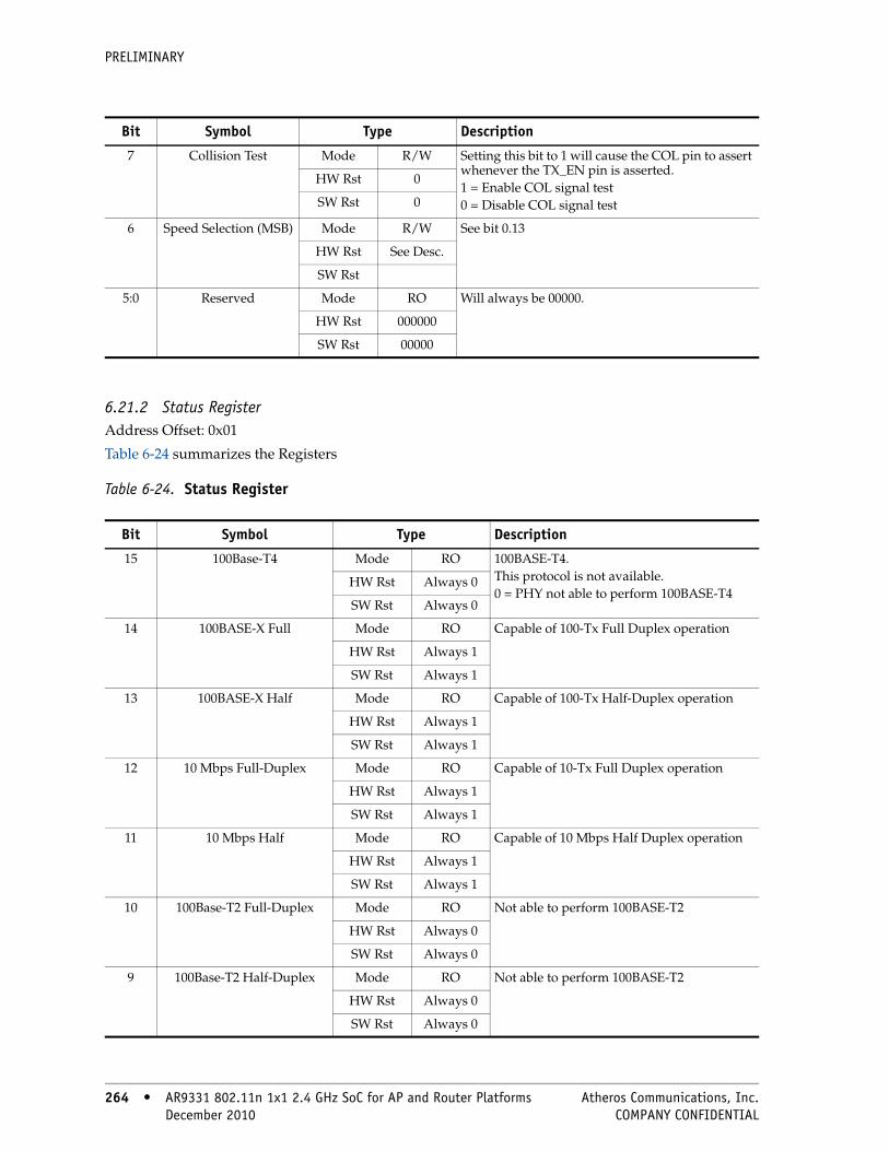
PRELIMINARY
6.21.2 Status RegisterAddress Offset: 0x01
Table 6-24 summarizes the Registers
Table 6-24. Status Register
7 Collision Test Mode R/W Setting this bit to 1 will cause the COL pin to assert whenever the TX_EN pin is asserted.1 = Enable COL signal test0 = Disable COL signal test
HW Rst 0
SW Rst 0
6 Speed Selection (MSB) Mode R/W See bit 0.13
HW Rst See Desc.
SW Rst
5:0 Reserved Mode RO Will always be 00000.
HW Rst 000000
SW Rst 00000
Bit Symbol Type Description
Bit Symbol Type Description
15 100Base-T4 Mode RO 100BASE-T4.This protocol is not available.0 = PHY not able to perform 100BASE-T4
HW Rst Always 0
SW Rst Always 0
14 100BASE-X Full Mode RO Capable of 100-Tx Full Duplex operation
HW Rst Always 1
SW Rst Always 1
13 100BASE-X Half Mode RO Capable of 100-Tx Half-Duplex operation
HW Rst Always 1
SW Rst Always 1
12 10 Mbps Full-Duplex Mode RO Capable of 10-Tx Full Duplex operation
HW Rst Always 1
SW Rst Always 1
11 10 Mbps Half Mode RO Capable of 10 Mbps Half Duplex operation
HW Rst Always 1
SW Rst Always 1
10 100Base-T2 Full-Duplex Mode RO Not able to perform 100BASE-T2
HW Rst Always 0
SW Rst Always 0
9 100Base-T2 Half-Duplex Mode RO Not able to perform 100BASE-T2
HW Rst Always 0
SW Rst Always 0
264 • AR9331 802.11n 1x1 2.4 GHz SoC for AP and Router Platforms Atheros Communications, Inc. 264 • December 2010 COMPANY CONFIDENTIAL

PRELIMINARY
8 Extended Status Mode RO Extended status information in register15
HW Rst Always 0
SW Rst Always 0
7 Reserved Mode RO Always 0
HW Rst Always 0
SW Rst Always 0
6 MF Preamble Suppression Mode RO PHY accepts management frames with preamble suppressed
HW Rst Always 1
SW Rst Always 1
5 Auto-negotiation Complete Mode RO 1 = Auto negotiation process complete0 = Auto negotiation process not completeHW Rst 0
SW Rst 0
4 Remote Fault Mode RO, LH 1 = Remote fault condition detected0 = Remote fault condition not detectedHW Rst 0
SW Rst 0
3 Auto-negotiation Ability Mode RO 1 = PHY able to perform auto negotiation
HW Rst Always 1
SW Rst Always 1
2 Link Status Mode RO, LL This register bit indicates whether the link was lost since the last read. For the current link status, readregister bit 17.10 Link Real Time.1 = Link is up0 = Link is down
HW Rst 0
SW Rst 0
1 Jabber Detect Mode RO, LH 1 = Jabber condition detected0 = Jabber condition not detectedHW Rst 0
SW Rst 0
0 Extended Capability Mode RO 1 = Extended register capabilities
HW Rst Always 1
SW Rst Always 1
Bit Symbol Type Description
Atheros Communications, Inc. AR9331 802.11n 1x1 2.4 GHz SoC for AP and Router Platforms • 265 COMPANY CONFIDENTIAL December 2010 • 265
PRELIMINARY
6.21.3 PHY IdentifierAddress Offset: 0x02
Table 6-25 summarizes the Registers
Table 6-25. PHY Identifier
6.21.4 PHY Identifier 2Address Offset: 0x03
Table 6-26 summarizes the Registers
Table 6-26. PHY Identifier 2
Bit Symbol Type Description
15:0 Organizationally Unique Identifer Bit 3:18
Mode RO Organizationally Unique Identifier bits 3:18
HW Rst Always 16’h004d
SW Rst Always 16’h004d
Bit Symbol Type Description
15 OUI LSB Model Number Revision Number
Mode RO Organizationally Unique Identifier bits 19:24
HW Rst Always 16’hd041
SW Rst Always 16’hd041
266 • AR9331 802.11n 1x1 2.4 GHz SoC for AP and Router Platforms Atheros Communications, Inc. 266 • December 2010 COMPANY CONFIDENTIAL
PRELIMINARY
6.21.5 Auto-negotiation Advertisement RegisterAddress Offset: 0x04
Table 6-27 summarizes the Registers
Table 6-27. Auto-negotiation Advertisement Register
Bit Symbol Type Description
15 Next Page Mode R/W The value of this bit will be updated immediately after writing this register. But the value written to this bit does not takes effect until any one of the following occurs:■ Software reset is asserted (register 0.15)■ Restart Auto-Negotiation is asserted (register 0.9)■ Power down (register 0.11) transitions from power
down to normal operation■ Link goes down
Register 4.15 should be set to 0 if no additional next pages are needed.1 = Advertise0 = Not advertised
HW Rst 0
SW Rst Update
14 Ack Mode RO Must be 0
HW Rst Always 0
SW Rst Always 0
13 Remote Fault Mode R/W 1 = Set Remote Fault bit0 = Do not set Remote Fault bitHW Rst Always 0
SW Rst Always 0
12 Reserved Mode RO Always 0.
HW Rst Always 0
SW Rst Always 0
11 Asymmetric Pause Mode R/W The value of this bit will be updated immediately after writing this register. But the value written to this bit does not takes effect until any one of the following occurs:
■ Software reset is asserted (register 0.15)■ Restart Auto-Negotiation is asserted (register 0.9)■ Power down (register 0.11) transitions from power
down to normal operation■ Link goes down
1 = Asymmetric Pause0 = No asymmetric Pause(This bit has added the pad control and can be set from the F001 top. Its default value is one)
HW Rst 1
SW Rst Update
Atheros Communications, Inc. AR9331 802.11n 1x1 2.4 GHz SoC for AP and Router Platforms • 267 COMPANY CONFIDENTIAL December 2010 • 267

PRELIMINARY
10 PAUSE Mode R/W The value of this bit will be updated immediately after writing this register. But the value written to this bit does not takes effect until any one of the following occurs:
■ Software reset is asserted (register 0.15)■ Restart Auto-Negotiation is asserted (register 0.9)■ Power down (register 0.11) transitions from power
down to normal operation■ Link goes down
1 = MAC PAUSE implemented0 = MAC PAUSE not implemented(This bit has added the pad control and can be set from the F001 top. Its default value is one)
HW Rst 1
SW Rst Update
9 100Base-T4 Mode RO Not able to perform 100BASE-T4
HW Rst Always 0
SW Rst Always 0
8 100Base -TX Mode R/W The value of this bit will be updated immediately after writing this register. But the value written to this bit does not takes effect until any one of the following occurs:
■ Software reset is asserted (register 0.15)■ Restart Auto-Negotiation is asserted (register 0.9)■ Power down (register 0.11) transitions from power
down to normal operation■ Link goes down
1 = Advertise0 = Not advertised
HW Rst 1
SW Rst Update
7 100BASE-TXHalf Duplex
Mode R/W The value of this bit will be updated immediately after writing this register. But the value written to this bit does not takes effect until any one of the following occurs:
■ Software reset is asserted (register 0.15)■ Restart Auto-Negotiation is asserted (register 0.9)■ Power down (register 0.11) transitions from power
down to normal operation■ Link goes down
1 = Advertise0 = Not advertised
HW Rst 1
SW Rst Update
6 10BASE-TXFull Duplex
Mode R/W The value of this bit will be updated immediately after writing this register. But the value written to this bit does not takes effect until any one of the following occurs:
■ Software reset is asserted (register 0.15)■ Restart Auto-Negotiation is asserted (register 0.9)■ Power down (register 0.11) transitions from power
down to normal operation■ Link goes down
1 = Advertise0 = Not advertised
HW Rst 1
SW Rst Update
Bit Symbol Type Description
268 • AR9331 802.11n 1x1 2.4 GHz SoC for AP and Router Platforms Atheros Communications, Inc. 268 • December 2010 COMPANY CONFIDENTIAL

PRELIMINARY
6.21.6 Link Partner Ability RegisterAddress Offset: 0x05
Table 6-28 summarizes the Registers
Table 6-28. Link Partner Ability Register
5 10BASE-TXHalf Duplex
Mode R/W The value of this bit will be updated immediately after writing this register. But the value written to this bit does not takes effect until any one of the following occurs:
■ Software reset is asserted (register 0.15)■ Restart Auto-Negotiation is asserted (register 0.9)■ Power down (register 0.11) transitions from power
down to normal operation■ Link goes down
1 = Advertise0 = Not advertised
HW Rst 1
SW Rst Update
4:0 Selector Field Mode RO Selector Field mode00001 = 802.3HW Rst Always
00001
SW Rst Always 00001
Bit Symbol Type Description
Bit Symbol Type Description
15 Next Page Mode RO Received Code Word Bit 151 = Link partner capable of next page0 = Link partner not capable of next page
HW Rst 0
SW Rst 0
14 Ack Mode RO AcknowledgeReceived Code Word Bit 141 = Link partner received link code word0 = Link partner does not have Next Page ability
HW Rst 0
SW Rst 0
13 Remote Fault Mode RO Remote FaultReceived Code Word Bit 131 = Link partner detected remote fault0 = Link partner has not detected remote fault
HW Rst 0
SW Rst 0
12 Reserved Mode RO Technology Ability FieldReceived Code Word Bit 12HW Rst 0
SW Rst 0
11 Asymmetric Pause Mode RO Technology Ability FieldReceived Code Word Bit 111 = Link partner requests asymmetric pause0 = Link partner does not request asymmetric pause
HW Rst 0
SW Rst 0
Atheros Communications, Inc. AR9331 802.11n 1x1 2.4 GHz SoC for AP and Router Platforms • 269 COMPANY CONFIDENTIAL December 2010 • 269
PRELIMINARY
6.21.7 Auto-negotiation Expansion RegisterAddress Offset: 0x06
Table 6-29 summarizes the Registers
Table 6-29. Auto-negotiation Expansion Register
10 PAUSE Mode RO Technology Ability FieldReceived Code Word Bit 101 = Link partner is capable of pause operation0 = Link partner is not capable of pause operation
HW Rst 0
SW Rst 0
9 100BASE-T4 Mode Technology Ability FieldReceived Code Word Bit 91 = Link partner is 100BASE-T4 capable0 = Link partner is not 100BASE-T4 capable
HW Rst
SW Rst
8 100BASE-TXFull Duplex
Mode RO Technology Ability FieldReceived Code Word Bit 81 = Link partner is 100BASE-TX full-duplex capable0 = Link partner is not 100BASE-TX full-duplex capable
HW Rst 0
SW Rst 0
7 100BASE-TXHalf Duplex
Mode RO Technology Ability FieldReceived Code Word Bit 71 = Link partner is 100BASE-TX half-duplex capable0 = Link partner is not 100BASE-TX half-duplex capable
HW Rst 0
SW Rst 0
6 10BASE-TXFull Duplex
Mode RO Technology Ability FieldReceived Code Word Bit 61 = Link partner is 10BASE-T full-duplex capable0 = Link partner is not 10BASE-T full-duplex capable
HW Rst 0
SW Rst 0
5 10BASE-TXHalf Duplex
Mode RO Technology Ability FieldReceived Code Word Bit 51 = Link partner is 10BASE-T half-duplex capable0 = Link partner is not 10BASE-T half-duplex capable
HW Rst 0
SW Rst 0
4:0 Selector field Mode RO Selector FieldReceived Code Word Bit 4:0HW Rst 00000
SW Rst 00000
Bit Symbol Type Description
Bit Symbol Type Description
15:5 Reserved Mode RO Reserved. Must be 0.
HW Rst Always 0x000
SW Rst Always 0x000
270 • AR9331 802.11n 1x1 2.4 GHz SoC for AP and Router Platforms Atheros Communications, Inc. 270 • December 2010 COMPANY CONFIDENTIAL
PRELIMINARY
6.21.8 Next Page Transmit RegisterAddress Offset: 0x07
Table 6-30 summarizes the Registers
Table 6-30. Next Page Transmit Register
4 Parallel Detection Fault Mode RO, LH 1 = A fault has been detect 0 = No fault has been detected HW Rst 0
SW Rst 0
3 Link Partner Next Page Able Mode RO 1 = Link partner is Next page able0 = Link partner is not next page ableHW Rst 0
SW Rst 0
2 Local Next Page Able Mode R/W 1 = Local Device is Next Page able
HW Rst 1
SW Rst 1
1 Page Received Mode RO, LH 1 = A new page has been received0 = No new page has been receivedHW Rst 0
SW Rst 0
0 Link Partner Auto-negotiation Able
Mode RO 1 = Link partner is auto negotiation able0 = Link partner is not auto negotiation able HW Rst 0
SW Rst 0
Bit Symbol Type Description
Bit Symbol Type Description
15 Next Page Mode R/W Transmit Code Word Bit 15
HW Rst 0
SW Rst 0
14 Reserved Mode R/W Transmit Code Word Bit 14
HW Rst 0
SW Rst 0
13 Message Page Mode Mode R/W Transmit Code Word Bit 13
HW Rst 0
SW Rst 0
12 Ack Mode R/W Transmit Code Word Bit 12
HW Rst 0
SW Rst 0
11 Toggle Mode RO Transmit Code Word Bit 11
HW Rst 0
SW Rst 0
Atheros Communications, Inc. AR9331 802.11n 1x1 2.4 GHz SoC for AP and Router Platforms • 271 COMPANY CONFIDENTIAL December 2010 • 271

PRELIMINARY
6.21.9 Link Partner Next Page RegisterAddress Offset: 0x08
Table 6-31 summarizes the Registers
Table 6-31. Link Partner Next Page Register
10:0 Message/Unformatted Field Mode R/W Transmit Code Word Bit 10:0
HW Rst 0x001
SW Rst 0x001
Bit Symbol Type Description
Bit Symbol Type Description
15 Next Page Mode RO Received Code Word Bit 15
HW Rst 0
SW Rst 0
14 Reserved Mode RO Received Code Word Bit 14
HW Rst 0
SW Rst 0
13 Message Page Mode Mode RO Received Code Word Bit 13
HW Rst 0
SW Rst 0
12 Ack2 Mode RO Received Code Word Bit 12
HW Rst 0
SW Rst 0
11 Toggle Mode RO Received Code Word Bit 11
HW Rst 0
SW Rst 0
10:0 Message/Unformatted Field
Mode R/W Received Code Word Bit 10:0
HW Rst 0x000
SW Rst 0x000
272 • AR9331 802.11n 1x1 2.4 GHz SoC for AP and Router Platforms Atheros Communications, Inc. 272 • December 2010 COMPANY CONFIDENTIAL
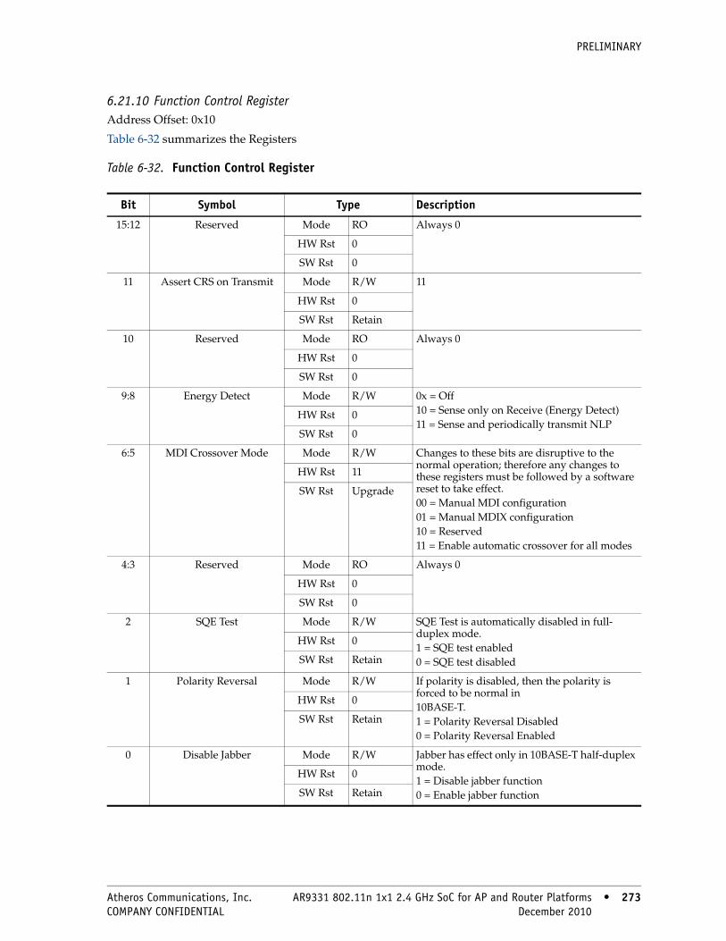
PRELIMINARY
6.21.10 Function Control RegisterAddress Offset: 0x10
Table 6-32 summarizes the Registers
Table 6-32. Function Control Register
Bit Symbol Type Description
15:12 Reserved Mode RO Always 0
HW Rst 0
SW Rst 0
11 Assert CRS on Transmit Mode R/W 11
HW Rst 0
SW Rst Retain
10 Reserved Mode RO Always 0
HW Rst 0
SW Rst 0
9:8 Energy Detect Mode R/W 0x = Off10 = Sense only on Receive (Energy Detect)11 = Sense and periodically transmit NLP
HW Rst 0
SW Rst 0
6:5 MDI Crossover Mode Mode R/W Changes to these bits are disruptive to the normal operation; therefore any changes to these registers must be followed by a software reset to take effect.00 = Manual MDI configuration01 = Manual MDIX configuration10 = Reserved11 = Enable automatic crossover for all modes
HW Rst 11
SW Rst Upgrade
4:3 Reserved Mode RO Always 0
HW Rst 0
SW Rst 0
2 SQE Test Mode R/W SQE Test is automatically disabled in full-duplex mode.1 = SQE test enabled0 = SQE test disabled
HW Rst 0
SW Rst Retain
1 Polarity Reversal Mode R/W If polarity is disabled, then the polarity is forced to be normal in10BASE-T.1 = Polarity Reversal Disabled0 = Polarity Reversal Enabled
HW Rst 0
SW Rst Retain
0 Disable Jabber Mode R/W Jabber has effect only in 10BASE-T half-duplex mode.1 = Disable jabber function0 = Enable jabber function
HW Rst 0
SW Rst Retain
Atheros Communications, Inc. AR9331 802.11n 1x1 2.4 GHz SoC for AP and Router Platforms • 273 COMPANY CONFIDENTIAL December 2010 • 273

PRELIMINARY
6.21.11 PHY Specific Status RegisterAddress Offset: 0x11
Table 6-33 summarizes the Registers
Table 6-33. PHY Specific Status Register
Bit Symbol Type Description
15:14 Speed Mode RO These status bits are valid when Auto-Negotiation is completed or Auto-Negotiation is disabled.11 = Reserved10 = Reserved01 = 100 Mbps00 = 10 Mbps
HW Rst 00
SW Rst Retain
13 Duplex Mode RO This status bit is valid only when Auto-Negotiation is complete or disabled.‘1’ = Full-Duplex‘0’ = Half-Duplex
HW Rst 0
SW Rst Retain
12 Page Received (Real Time) Mode RO 1 = Page received0 = Page not receivedHW Rst 0
SW Rst Retain
11 Speed and Duplex Resolved
Mode RO When Auto-Negotiation is not enabled for force speed mode.1 = Resolved0 = Not resolved
HW Rst 0
SW Rst 0
10 Link (Real Time) Mode RO 1 = Link up0 = Link downHW Rst 0
SW Rst 0
9:7 Reserved Mode RO Always 0
HW Rst 0
SW Rst 0
6 MDI CrossoverStatus
Mode RO This status bit is valid only when Auto-Negotiation is completed or Auto-Negotiation is disabled. 1 = MDIX0 = MDI
HW Rst 0
SW Rst Retain
5 Wirespeed downgrade Mode RO 1 = Downgrade0 = No DowngradeHW Rst 0
SW Rst 0
4 Energy Detect Status Mode RO 1 = Sleep0 = ActiveHW Rst 0
SW Rst 0
274 • AR9331 802.11n 1x1 2.4 GHz SoC for AP and Router Platforms Atheros Communications, Inc. 274 • December 2010 COMPANY CONFIDENTIAL
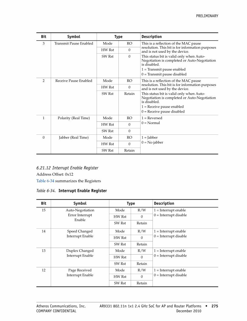
PRELIMINARY
6.21.12 Interrupt Enable RegisterAddress Offset: 0x12
Table 6-34 summarizes the Registers
Table 6-34. Interrupt Enable Register
3 Transmit Pause Enabled Mode RO This is a reflection of the MAC pause resolution. This bit is for information purposes and is not used by the device.This status bit is valid only when Auto-Negotiation is completed or Auto-Negotiation is disabled.1 = Transmit pause enabled0 = Transmit pause disabled
HW Rst 0
SW Rst 0
2 Receive Pause Enabled Mode RO This is a reflection of the MAC pause resolution. This bit is for information purposes and is not used by the device.This status bit is valid only when Auto-Negotiation is completed or Auto-Negotiation is disabled.1 = Receive pause enabled0 = Receive pause disabled
HW Rst 0
SW Rst Retain
1 Polarity (Real Time) Mode RO 1 = Reversed0 = NormalHW Rst 0
SW Rst 0
0 Jabber (Real Time) Mode RO 1 = Jabber0 = No jabberHW Rst 0
SW Rst Retain
Bit Symbol Type Description
Bit Symbol Type Description
15 Auto-NegotiationError Interrupt
Enable
Mode R/W 1 = Interrupt enable0 = Interrupt disableHW Rst 0
SW Rst Retain
14 Speed ChangedInterrupt Enable
Mode R/W 1 = Interrupt enable0 = Interrupt disableHW Rst 0
SW Rst Retain
13 Duplex ChangedInterrupt Enable
Mode R/W 1 = Interrupt enable0 = Interrupt disableHW Rst 0
SW Rst Retain
12 Page ReceivedInterrupt Enable
Mode R/W 1 = Interrupt enable0 = Interrupt disableHW Rst 0
SW Rst Retain
Atheros Communications, Inc. AR9331 802.11n 1x1 2.4 GHz SoC for AP and Router Platforms • 275 COMPANY CONFIDENTIAL December 2010 • 275
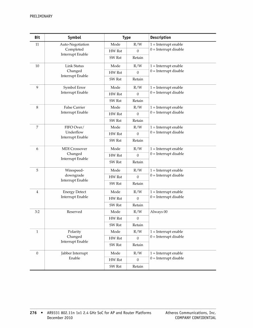
PRELIMINARY
11 Auto-NegotiationCompleted
Interrupt Enable
Mode R/W 1 = Interrupt enable0 = Interrupt disableHW Rst 0
SW Rst Retain
10 Link StatusChanged
Interrupt Enable
Mode R/W 1 = Interrupt enable0 = Interrupt disableHW Rst 0
SW Rst Retain
9 Symbol ErrorInterrupt Enable
Mode R/W 1 = Interrupt enable0 = Interrupt disableHW Rst 0
SW Rst Retain
8 False CarrierInterrupt Enable
Mode R/W 1 = Interrupt enable0 = Interrupt disableHW Rst 0
SW Rst Retain
7 FIFO Over/Underflow
Interrupt Enable
Mode R/W 1 = Interrupt enable0 = Interrupt disableHW Rst 0
SW Rst Retain
6 MDI CrossoverChanged
Interrupt Enable
Mode R/W 1 = Interrupt enable0 = Interrupt disableHW Rst 0
SW Rst Retain
5 Wirespeed-downgrade
Interrupt Enable
Mode R/W 1 = Interrupt enable0 = Interrupt disableHW Rst 0
SW Rst Retain
4 Energy DetectInterrupt Enable
Mode R/W 1 = Interrupt enable0 = Interrupt disableHW Rst 0
SW Rst Retain
3:2 Reserved Mode R/W Always 00
HW Rst 0
SW Rst Retain
1 PolarityChanged
Interrupt Enable
Mode R/W 1 = Interrupt enable0 = Interrupt disableHW Rst 0
SW Rst Retain
0 Jabber InterruptEnable
Mode R/W 1 = Interrupt enable0 = Interrupt disableHW Rst 0
SW Rst Retain
Bit Symbol Type Description
276 • AR9331 802.11n 1x1 2.4 GHz SoC for AP and Router Platforms Atheros Communications, Inc. 276 • December 2010 COMPANY CONFIDENTIAL

PRELIMINARY
6.21.13 Interrupt Status RegisterAddress Offset: 0x13
Table 6-35. Interrupt Status Register
Bit Symbol Type Description15 Auto-Negotiation
ErrorMode RO, LH An error is said to occur if MASTER/SLAVE
does not resolve, parallel detect fault, no common HCD, or link does not come up after negotiation is completed.1 = Auto-Negotiation Error0 = No Auto-Negotiation Error
HW Rst 0
SW Rst Retain
14 Speed Changed Mode RO, LH 1 = Speed changed0 = Speed not changedHW Rst 0
SW Rst Retain
13 Reserved Mode RO, LH Reserved
HW Rst 0
SW Rst Retain
12 Page Received Mode RO 1 = Page received0 = Page not receivedHW Rst 0
SW Rst Retain
11 Auto-NegotiationCompleted
Mode RO 1 = Auto-Negotiation completed0 = Auto-Negotiation not completedHW Rst 0
SW Rst Retain
10 Link StatusChanged
Mode RO, LH 1 = Link status changed0 = Link status not changedHW Rst 0
SW Rst Retain
9 Symbol Error Mode RO, LH 1 = Symbol error0 = No symbol errorHW Rst 0
SW Rst Retain
8 False Carrier Mode RO, LH 1 = False carrier0 = No false carrierHW Rst 0
SW Rst Retain
7 FIFO Over/Underflow Mode RO, LH 1 = Over/Underflow Error0 = No FIFO Error
Not implement, always 0.
HW Rst 0
SW Rst Retain
6 MDI CrossoverChanged
Mode RO, LH 1 = Crossover changed0 = Crossover not changedHW Rst 0
SW Rst Retain
5 Wirespeed-downgrade
Interrupt
Mode RO, LH 1 = Wirespeed-downgrade detected.0 = No Wirespeed-downgrade.HW Rst 0
SW Rst Retain
4 Energy Detect Changed Mode RO, LH 1 = Energy Detect state changed0 = No Energy Detect state change detected
Not implement, always 0.
HW Rst 0
SW Rst Retain
Atheros Communications, Inc. AR9331 802.11n 1x1 2.4 GHz SoC for AP and Router Platforms • 277 COMPANY CONFIDENTIAL December 2010 • 277

PRELIMINARY
6.21.14 Smart Speed RegisterAddress Offset: 0x14
Table 6-36 summarizes the Registers
Table 6-36. Smart Speed Register
3:2 Reserved Mode RO, LH Always 0
HW Rst 0
SW Rst Retain
1 PolarityChanged
Mode RO, LH 1 = Polarity Changed0 = Polarity not changedHW Rst 0
SW Rst Retain
0 Jabber Mode RO, LH 1 = Jabber0 = No jabberHW Rst 0
SW Rst Retain
Bit Symbol Type Description
Bit Symbol Type Description
15:11 Reserved Mode RO Reserved. must be 00000000
HW Rst 0
SW Rst 0
10 aneg_now_qual Mode R/W A rise of input pin "aneg_now" will set this bit to 1'b2, and cause PHY to restart auto-negotiation. Self-clear.
HW Rst 1’b0
SW Rst Retain
9 Rev_aneg_qual Mode R/W Make PHY to auto-negotiate in reversed mode. This bit takes its value from the input pin "rev_aneg" upon following:1 HW reset (fall of rst_dsp_i);2 PHY SW reset;3 Rise of aneg_now.
HW Rst 1’b0
SW Rst Update
8 Giga_dis_qual Mode R/W Make PHY to disable GIGA mode. This bit takes its value from the input pin "giga_dis" upon following:1 HW reset (fall of rst_dsp_i);2 PHY SW reset;3 Rise of aneg_now.
HW Rst 1’b0
SW Rst Update
7 Cfg_pad_en Mode RO, LH The default value is zero; if this bit is set to one, then the auto negotiation Arbitration FSM will bypass the LINK_STATUS_CHECK state when the 10 BaseT/100 BaseT ready signal is asserted.
HW Rst 0
SW Rst Retain
6 Mr_ltdis Mode R/W The default value is zero; if this bit is set to one, then the NLP Receive Link Integrity Test FSM will stays at the NLP_TEST_PASS state.HW Rst 0
SW Rst Update
278 • AR9331 802.11n 1x1 2.4 GHz SoC for AP and Router Platforms Atheros Communications, Inc. 278 • December 2010 COMPANY CONFIDENTIAL
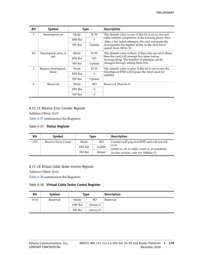
PRELIMINARY
6.21.15 Receive Error Counter RegisterAddress Offset: 0x15
Table 6-37 summarizes the Registers
Table 6-37. Status Register
6.21.16 Virtual Cable Tester Control RegisterAddress Offset: 0x16
Table 6-38 summarizes the Registers
Table 6-38. Virtual Cable Tester Contol Register
5 Smartspeed_en Mode R/W The default value is one; if this bit is set to one and cable inhibits completion of the training phase, thenAfter a few failed attempts, the card automatically downgrades the highest ability to the next lower speed: from 100 to 10.
HW Rst 1
SW Rst Update
4:2 Smartspeed_retry_limit
Mode R/W The default value is three; if these bits are set to three, then the card will attempt five times before downgrading; The number of attempts can be changed through setting these bits.
HW Rst 011
SW Rst Update
1 Bypass_smartspeed_ timer
Mode R/W The default value is zero; if this bit is set to one, the Smartspeed FSM will bypass the timer used for stability.HW Rst 0
SW Rst Update
0 Reserved Mode RO Reserved. Must be 0.
HW Rst 0
SW Rst 0
Bit Symbol Type Description
Bit Symbol Type Description
15:0 Receive Error Count Mode RO Counter will peg at 0xFFFF and will not roll over.(when rx_dv is valid, count rx_er numbers)(in this version, only for 100Base-T)
HW Rst 0x0000
SW Rst Retain
Bit Symbol Type Description
15:10 Reserved Mode RO Reserved
HW Rst Always 0
SW Rst Always 0
Atheros Communications, Inc. AR9331 802.11n 1x1 2.4 GHz SoC for AP and Router Platforms • 279 COMPANY CONFIDENTIAL December 2010 • 279
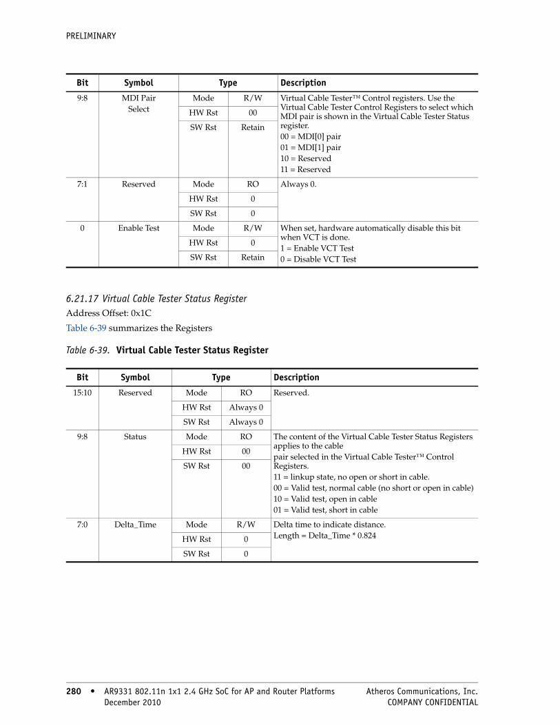
PRELIMINARY
6.21.17 Virtual Cable Tester Status RegisterAddress Offset: 0x1C
Table 6-39 summarizes the Registers
Table 6-39. Virtual Cable Tester Status Register
9:8 MDI PairSelect
Mode R/W Virtual Cable Tester™ Control registers. Use the Virtual Cable Tester Control Registers to select which MDI pair is shown in the Virtual Cable Tester Status register.00 = MDI[0] pair01 = MDI[1] pair10 = Reserved11 = Reserved
HW Rst 00
SW Rst Retain
7:1 Reserved Mode RO Always 0.
HW Rst 0
SW Rst 0
0 Enable Test Mode R/W When set, hardware automatically disable this bit when VCT is done.1 = Enable VCT Test0 = Disable VCT Test
HW Rst 0
SW Rst Retain
Bit Symbol Type Description
Bit Symbol Type Description
15:10 Reserved Mode RO Reserved.
HW Rst Always 0
SW Rst Always 0
9:8 Status Mode RO The content of the Virtual Cable Tester Status Registers applies to the cablepair selected in the Virtual Cable Tester™ Control Registers.11 = linkup state, no open or short in cable.00 = Valid test, normal cable (no short or open in cable)10 = Valid test, open in cable01 = Valid test, short in cable
HW Rst 00
SW Rst 00
7:0 Delta_Time Mode R/W Delta time to indicate distance. Length = Delta_Time * 0.824HW Rst 0
SW Rst 0
280 • AR9331 802.11n 1x1 2.4 GHz SoC for AP and Router Platforms Atheros Communications, Inc. 280 • December 2010 COMPANY CONFIDENTIAL
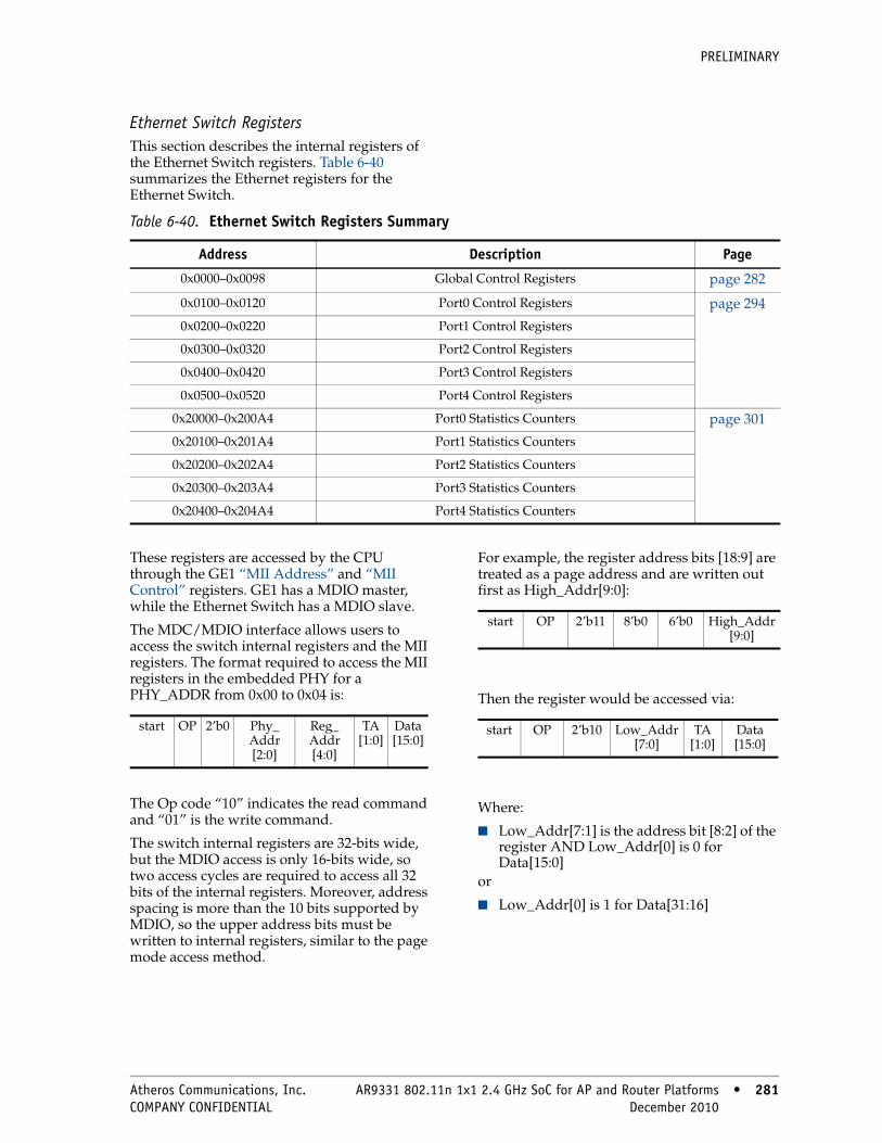
PRELIMINARY
Ethernet Switch RegistersThis section describes the internal registers of the Ethernet Switch registers. Table 6-40 summarizes the Ethernet registers for the Ethernet Switch.
These registers are accessed by the CPU through the GE1 “MII Address” and “MII Control” registers. GE1 has a MDIO master, while the Ethernet Switch has a MDIO slave.
The MDC/MDIO interface allows users to access the switch internal registers and the MII registers. The format required to access the MII registers in the embedded PHY for a PHY_ADDR from 0x00 to 0x04 is:
The Op code “10” indicates the read command and “01” is the write command.
The switch internal registers are 32-bits wide, but the MDIO access is only 16-bits wide, so two access cycles are required to access all 32 bits of the internal registers. Moreover, address spacing is more than the 10 bits supported by MDIO, so the upper address bits must be written to internal registers, similar to the page mode access method.
For example, the register address bits [18:9] are treated as a page address and are written out first as High_Addr[9:0]:
Then the register would be accessed via:
Where:
■ Low_Addr[7:1] is the address bit [8:2] of the register AND Low_Addr[0] is 0 for Data[15:0]
or
■ Low_Addr[0] is 1 for Data[31:16]
Table 6-40. Ethernet Switch Registers Summary
Address Description Page
0x0000–0x0098 Global Control Registers page 282
0x0100–0x0120 Port0 Control Registers page 294
0x0200–0x0220 Port1 Control Registers
0x0300–0x0320 Port2 Control Registers
0x0400–0x0420 Port3 Control Registers
0x0500–0x0520 Port4 Control Registers
0x20000–0x200A4 Port0 Statistics Counters page 301
0x20100–0x201A4 Port1 Statistics Counters
0x20200–0x202A4 Port2 Statistics Counters
0x20300–0x203A4 Port3 Statistics Counters
0x20400–0x204A4 Port4 Statistics Counters
start OP 2’b0 Phy_ Addr [2:0]
Reg_ Addr [4:0]
TA[1:0]
Data[15:0]
start OP 2’b11 8’b0 6’b0 High_Addr[9:0]
start OP 2’b10 Low_Addr[7:0]
TA[1:0]
Data[15:0]
Atheros Communications, Inc. AR9331 802.11n 1x1 2.4 GHz SoC for AP and Router Platforms • 281 COMPANY CONFIDENTIAL December 2010 • 281

PRELIMINARY
6.22 Global Control RegistersTable 6-41 summarizes the global control registers for the AR9331.
6.22.1 Global Mask ControlAddress: 0x0000 Access: Read/Write Reset: See field description
This register is used for soft resets.
Table 6-41. Global Control Registers
Offset Register Page
0x0000 Global Mask Control page 282
0x0010 Global Interrupt page 283
0x0014 Global Interrupt Mask page 284
0x0020 Global MAC Address 0 page 285
0x0024 Global MAC Address 1 page 284
0x002C Flood Mask page 285
0x0030 Global Control page 286
0x0040 VLAN Table Function 0 page 286
0x0044 VLAN Table Function 1 page 287
0x0050 Address Table Function 0 page 287
0x0054 Address Table Function 1 page 288
0x0058 Address Table Function 2 page 288
0x005C Address Table Control page 289
0x0060 IP Priority Mapping 0 page 289
0x0064 IP Priority Mapping 1 page 290
0x0068 IP Priority Mapping 2 page 290
0x006C IP Priority Mapping 3 page 291
0x0070 Tag Priority Mapping page 291
0x0074 Service Tag page 292
0x0078 CPU Port page 292
0x0080 MIB Function0 page 292
0x0098 MDIO Control page 293
Bit Bit Name Type Reset Description
31 SOFT_RET WO 0x0 Software reset. This bit is set by software to initialize the hardware, and should be self-cleared by hardware after the initialization is done.
30:0 RES RO 0x0 Reserved.
282 • AR9331 802.11n 1x1 2.4 GHz SoC for AP and Router Platforms Atheros Communications, Inc. 282 • December 2010 COMPANY CONFIDENTIAL

PRELIMINARY
6.22.2 Global Interrupt Address: 0x0010 Access: Read/Write Reset: 0x0
This register provides the status of various interrupts based global parameters. Interrupts are only generated when the corresponding bits of the following “Global Interrupt Mask” are set.
Bit Bit Name Description
31:18 RES Reserved. Must be written with zero. Contains zeros when read.
17 LOOKUP_ERR_INT Generates an interrupt when there is an error detected during a lookup
16 QM_ERR_INT This bit generates an interrupt when the QM detects an error
15 RES Reserved. Must be written with zero. Contains zeros when read.
14 HARDWARE_ INI_DONE
This bit generates an interrupt when the hardware memory initialization has completed
13 MIB_INI_INT This bit generates an interrupt when the MIB memory initialization has completed
12 MIB_DONE_ INT This bit generates an interrupt when the CPU has completed accessing the MIB
11 RES Reserved
10 VT_MISS_VIO_ INT This bit generates an interrupt when a VID is not located in the VLAN table
9 VT_MEM_VIO_INT This bit generates an interrupt when a VID is located in the VLAN table, yet the source port is not a member of the VID
8 VT_DONE_INT This bit generates an interrupt after completing an access to the VLAN table by the CPU
7 QM_INI_INT Generates an interrupt after the QM memory initialization is completed
6 AT_INI_INT Generates an interrupt when the address table initialization has completed
5 ARL_FULL_INT This bit generates an interrupt when there is an address attempting to be added to the address resolution table, yet the table is full
4 ARL_DONE_ INT This bit generates and interrupt when the address resolution table was accessed and the process has completed
3 MDIO_DONE_ INT Generates an interrupt when the MDIO access switch register is done
2 PHY_INT Generates an interrupt originating from the physical layer
1:0 RES Reserved
Atheros Communications, Inc. AR9331 802.11n 1x1 2.4 GHz SoC for AP and Router Platforms • 283 COMPANY CONFIDENTIAL December 2010 • 283

PRELIMINARY
6.22.3 Global Interrupt MaskAddress: 0x0014 Access: Read/Write Reset: See field description
This register controls various interrupts based global parameters. Interrupts are only generated when the bits of this register are set.
6.22.4 Global MAC Address 1Address: 0x0020 Access: Read/Write Reset: See field description
This register, along with the preceding “Global MAC Address 2”, are used to identify the station address of the switch.
Bit Bit Name Reset Description
31:18 RES 0x0 Reserved. Must be written with zero. Contains zeros when read.
17 LOOKUP_ERR_INT_EN
0x0 Enables an interrupt when there is an error detected during a lookup
16 QM_ERR_INT_EN 0x0 Enables an interrupt when the QM detects an error
15 RES 0x0 Reserved. Must be written with zero. Contains zeros when read.
14 HARDWARE_ INI_DONE_EN
0x0 Enables an interrupt when the hardware memory initialization has completed
13 MIB_INI_INT_ EN 0x0 Enables an interrupt when the MIB memory initialization has completed
12 MIB_DONE_ INT_EN
0x0 Enables an interrupt when the CPU is finished accessing the MIB
11 RES 0x0 Reserved
10 VT_MISS_VIO_ INT_EN
0x0 Enables an interrupt when a VID is not located in the VLAN table
9 VT_MEM_VIO_INT_EN
0x0 Enables an interrupt when a VID is located in the VLAN table, yet the source port is not a member of the VID
8 VT_DONE_INT_EN 0x0 Enables an interrupt after completing an access to the VLAN table by the CPU
7 QM_INI_INT_ EN 0x0 Enables an interrupt after the QM memory initialization has been completed
6 AT_INI_INT_ EN 0x0 Enables an interrupt when the address table initialization has completed
5 ARL_FULL_INT_EN 0x0 Enables an interrupt when there is an address attempting to be added to the address resolution table, yet the table is full
4 ARL_DONE_ INT_EN
0x0 Enables interrupt when the address resolution table was accessed and the process has completed
3 MDIO_DONE_ INT_EN
0x0 Enables an interrupt when the MDIO access switch register is done
2 PHY_INT_EN 0x0 Enables an interrupt originating from the physical layer
1:0 RES 0x0 Reserved
Bit Bit Name Reset Description
31:16 RES 0x0 Reserved
15:8 MAC_ADDR_ BYTE4 0x0 These bits represent the station address of the switch which is used as a source address in pause frames or other management frames
7:0 MAC_ADDR_ BYTE5 0x01
284 • AR9331 802.11n 1x1 2.4 GHz SoC for AP and Router Platforms Atheros Communications, Inc. 284 • December 2010 COMPANY CONFIDENTIAL
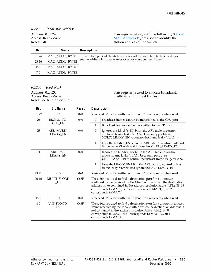
PRELIMINARY
6.22.5 Global MAC Address 2Address: 0x0024 Access: Read/Write Reset: 0x0
This register, along with the following “Global MAC Address 1”, are used to identify the station address of the switch.
6.22.6 Flood MaskAddress: 0x002C Access: Read/Write Reset: See field description
This register is used to allocate broadcast, multicast and unicast frames.
Bit Bit Name Description
31:24 MAC_ADDR_ BYTE0 These bits represent the station address of the switch, which is used as a source address in pause frames or other management frames
23:16 MAC_ADDR_ BYTE1
15:8 MAC_ADDR_ BYTE2
7:0 MAC_ADDR_ BYTE3
Bit Bit Name Reset Description
31:27 RES 0x0 Reserved. Must be written with zero. Contains zeros when read.
26 BROAD_TO_ CPU_EN
0x0 0 Broadcast frames cannot be transmitted to the CPU port
1 Broadcast frames can be transmitted to the CPU port
25 ARL_MULTI_ LEAKY_EN
0x0 0 Ignores the LEAKY_EN bit in the ARL table to control multicast frame leaky VLANs. Uses only port-base MULTI_LEAKY_EN to control the frame leaky VLAN.
1 Uses the LEAKY_EN bit in the ARL table to control multicast frame leaky VLANs and ignore the MULTI_LEAKY_EN
24 ARL_UNI_ LEAKY_EN
0x0 0 Ignores the LEAKY_EN bit in the ARL table to control unicast frame leaky VLAN. Uses only port-base UNI_LEAKY_EN to control the unicast frame leaky VLAN.
1 Uses the LEAKY_EN bit in the ARL table to control unicast frame leaky VLANs and ignore the UNI_LEAKY_EN
23:21 RES 0x0 Reserved. Must be written with zero. Contains zeros when read.
20:16 MULTI_FLOOD_DP
0x3F These bits are used to find a destination port for a unknown multicast frame received by the MAC, within which the destination address is not contained in the address resolution table (ARL). Bit 16 corresponds to MAC0, bit 17 corresponds to MAC1,..., bit 20 corresponds to MAC4.
15:5 RES 0x0 Reserved. Must be written with zero. Contains zeros when read.
4:0 UNI_FLOOD_ DP
0x3F These bits are used to find a destination port for a unknown unicast frame received by the MAC, within which the destination address is not contained in the address resolution table (ARL). Bit 0 corresponds to MAC0, bit 1 corresponds to MAC1,..., bit 4 corresponds to MAC4.
Atheros Communications, Inc. AR9331 802.11n 1x1 2.4 GHz SoC for AP and Router Platforms • 285 COMPANY CONFIDENTIAL December 2010 • 285
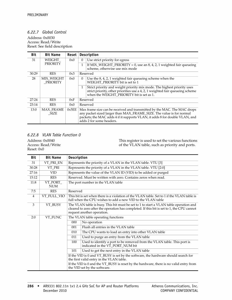
PRELIMINARY
6.22.7 Global ControlAddress: 0x0030 Access: Read/Write Reset: See field description
6.22.8 VLAN Table Function 0Address: 0x0040 Access: Read/Write Reset: 0x0
This register is used to set the various functions of the VLAN table, such as priority and ports.
Bit Bit Name Reset Description31 WEIGHT_
PRIORITY0x0 0 Use strict priority for egress
1 If MIX_WEIGHT_PRIORITY = 0, use an 8, 4, 2, 1 weighted fair queueing scheme, otherwise use mix mode
30:29 RES 0x3 Reserved28 MIX_WEIGHT
_PRIORITY0x0 0 Use the 8, 4, 2, 1 weighted fair queueing scheme when the
WEIGHT_PRIORITY bit is set to 11 Strict priority and weight priority mix mode. The highest priority uses
strict priority, other priorities use a 4, 2, 1 weighted fair queueing scheme when the WEIGHT_PRIORITY bit is set as 1.
27:24 RES 0xF Reserved23:14 RES 0x0 Reserved13:0 MAX_FRAME
_SIZE0x5EE Max frame size can be received and transmitted by the MAC. The MAC drops
any packet sized larger than MAX_FRAME_SIZE. The value is for normal packets; the MAC adds 4 if it supports VLAN, it adds 8 for double VLAN, and adds 2 for some headers.
Bit Bit Name Description31 VT_PRI_EN Represents the priority of a VLAN in the VLAN table. VTU [3]
30:28 VT_PRI Represents the priority of a VLAN in the VLAN table. VTU [2:0]27:16 VID Represents the value of the VLAN ID (VID) to be added or purged15:12 RES Reserved. Must be written with zero. Contains zeros when read.11:8 VT_PORT_
NUMThe port number in the VLAN table
7:5 RES Reserved4 VT_FULL_VIO This bit is set when there is a violation of the VLAN table. Set to 1 if the VLAN table is
full when the CPU wishes to add a new VID to the VLAN table3 VT_BUSY The VLAN table is busy. This bit must be set to 1 to start a VLAN table operation and
cleared to zero after the operation has completed. If this bit is set to 1, the CPU cannot request another operation.
2:0 VT_FUNC The VLAN table operating functions000 No operation001 Flush all entries in the VLAN table010 The CPU wants to load an entry into other VLAN table011 Used to purge an entry from the VLAN table100 Used to identify a port to be removed from the VLAN table. This port is
indicated in the VT_PORT_NUM bit101 Used to get the next entry in the VLAN table
If the VID is 0 and VT_BUSY is set by the software, the hardware should search for the first valid entry in the VLAN table.If the VID is 0 and the VT_BUSY is reset by the hardware, there is no valid entry from the VID set by the software.
286 • AR9331 802.11n 1x1 2.4 GHz SoC for AP and Router Platforms Atheros Communications, Inc. 286 • December 2010 COMPANY CONFIDENTIAL

PRELIMINARY
6.22.9 VLAN Table Function 1Address: 0x0044 Access: Read/Write Reset: 0x0
This register is used to identify VLAN entries in the VID table.
6.22.10 Address Table Function 0Address: 0x0050 Access: Read/Write Reset: 0x0
This register is used to configure functions of the address resolution (ARL) table.
Bit Bit Name Type Reset Description31:12 RES RO 0x0 Reserved. Must be written with zero. Contains zeros when read.
11 VT_VALID RW 0x0 Represents a valid entry in the VLAN table. VTU [15]10 RES RO 0x0 Reserved. Must be written with zero. Contains zeros when read.9:0 VID_MEM RW 0x0 Represents a VID member in the VLAN table. VTU [25:16]
Bit Bit Name Description31:24 AT_ADDR_
BYTES4The fifth byte of the address
23:16 AT_ADDR_ BYTES5
The last byte of the address
15:13 RES Reserved. Must be written with zero. Contains zeros when read.
12 AT_FULL_VIO
ARL table full violation. This bit is set to 1 if the ARL table is full when the CPU wishes to add a new entry into the ARL table, and if the ARL table is empty when the CPU wants to purge an entry from the ARL table.
11:8 AT_PORT_ NUM
The port number to be flushed. If the AT_FUNC is set to 101, the lookup module must flush all unicast entries for the port
7:5 RES Reserved. Must be written with zero. Contains zeros when read.
4 FLUSH_STATIC_EN
0 When the AT_FUNC is set to 101, only dynamic entries in the ARL table will be flushed
1 When the AT_FUNC is set to 101, static entries in the ARL table can be flushed
3 AT_BUSY The address table is busy. Setting this bit to 1 starts an ARL operation and it must be cleared to zero after the operation is complete. If set to 1, the CPU cannot request another operation
2:0 AT_FUNC The address table operation functions
000 No operation
001 Flush all entries
010 Used to load an entry. If these bits are set, the CPU wishes to load an entry into the ARL table
011 If these bits are set, used by the CPU to purge an entry from the ARL table
100 Flushes all unlocked entries from the ARL
101 Flushes the entries of one port from the Address table
110 Used to get the next valid or static entry in the ARL table
111 Setting these bits enables a MAC address to be searched
If the address and the AT_STATUS are both zero, the hardware will search the first valid entry from entry0.If the address is set to zero and the AT_STATUS is not zero, the hardware will discover the next valid entry which has an address of 0x0.If the hardware returns an address and the AT_STATUS is zero, there is no next valid entry in the address table.
Atheros Communications, Inc. AR9331 802.11n 1x1 2.4 GHz SoC for AP and Router Platforms • 287 COMPANY CONFIDENTIAL December 2010 • 287

PRELIMINARY
6.22.11 Address Table Function 1Address: 0x0054 Access: Read/Write Reset: 0x0
This register holds the address of the ARL table, along with bits [23:16] and [31:24] of the preceding “Address Table Function 0”.
6.22.12 Address Table Function 2Address: 0x0058 Access: Read/Write Reset: 0x0
This register is used to set parameters for the address resolution table (ARL) such as destination and source address.
Bit Bit Name Description
31:24 AT_ADDR_ BYTE0 The first byte of the address to operate. This byte is the highest byte of the MAC address for the most significant bit (MSB).
23:16 AT_ADDR_ BYTE1 The second byte of the address
15:8 AT_ADDR_ BYTE2 The third byte of the address
7:0 AT_ADDR_ BYTE3 The fourth byte of the address
Bit Bit Name Description
31:27 RES Reserved. Must be written with zero. Contains zeros when read.
26 COPY_TO_CPU ATU [7:0]
25 REDIRECT_TOCPU ATU [69]
24 LEAKY_EN Used to enable the leaky VLAN. ATU [68]
23:20 RES Reserved. Must be written with zero. Contains zeros when read.
19:16 AT_STATUS The destination address status. Associated with the “status” bits in the Address Table ATU [67:64]
15 RES Reserved. Must be written with zero. Contains zeros when read.
14 SA_DROP_EN Source address (SA) drop enable. ATU [62]
13 MIRROR_EN Setting this bit to 1 enables the copying of the DA frame to the mirror port. ATU [61]
12 AT_PRIORITY_EN Setting this bit to 1 enables the use of a DA priority. ATU [60]
11:10 AT_PRIORITY The destination address (DA) priority. ATU [59:58]
9:6 RES Reserved. Must be written with zero. Contains zeros when read.
5:0 DES_PORT The destination port bits for address ATU [53:48]
288 • AR9331 802.11n 1x1 2.4 GHz SoC for AP and Router Platforms Atheros Communications, Inc. 288 • December 2010 COMPANY CONFIDENTIAL
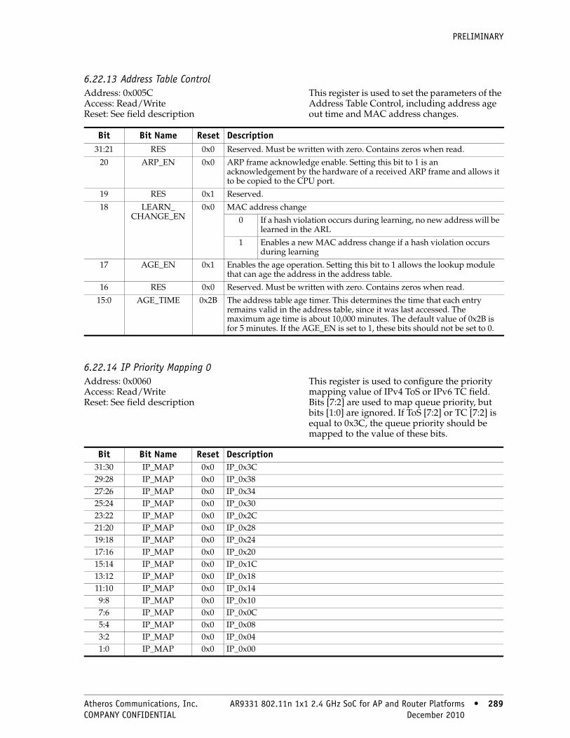
PRELIMINARY
6.22.13 Address Table ControlAddress: 0x005C Access: Read/Write Reset: See field description
This register is used to set the parameters of the Address Table Control, including address age out time and MAC address changes.
6.22.14 IP Priority Mapping 0Address: 0x0060 Access: Read/Write Reset: See field description
This register is used to configure the priority mapping value of IPv4 ToS or IPv6 TC field. Bits [7:2] are used to map queue priority, but bits [1:0] are ignored. If ToS [7:2] or TC [7:2] is equal to 0x3C, the queue priority should be mapped to the value of these bits.
Bit Bit Name Reset Description31:21 RES 0x0 Reserved. Must be written with zero. Contains zeros when read.
20 ARP_EN 0x0 ARP frame acknowledge enable. Setting this bit to 1 is an acknowledgement by the hardware of a received ARP frame and allows it to be copied to the CPU port.
19 RES 0x1 Reserved.
18 LEARN_ CHANGE_EN
0x0 MAC address change
0 If a hash violation occurs during learning, no new address will be learned in the ARL
1 Enables a new MAC address change if a hash violation occurs during learning
17 AGE_EN 0x1 Enables the age operation. Setting this bit to 1 allows the lookup module that can age the address in the address table.
16 RES 0x0 Reserved. Must be written with zero. Contains zeros when read.
15:0 AGE_TIME 0x2B The address table age timer. This determines the time that each entry remains valid in the address table, since it was last accessed. The maximum age time is about 10,000 minutes. The default value of 0x2B is for 5 minutes. If the AGE_EN is set to 1, these bits should not be set to 0.
Bit Bit Name Reset Description31:30 IP_MAP 0x0 IP_0x3C29:28 IP_MAP 0x0 IP_0x3827:26 IP_MAP 0x0 IP_0x3425:24 IP_MAP 0x0 IP_0x3023:22 IP_MAP 0x0 IP_0x2C21:20 IP_MAP 0x0 IP_0x2819:18 IP_MAP 0x0 IP_0x2417:16 IP_MAP 0x0 IP_0x2015:14 IP_MAP 0x0 IP_0x1C13:12 IP_MAP 0x0 IP_0x1811:10 IP_MAP 0x0 IP_0x149:8 IP_MAP 0x0 IP_0x107:6 IP_MAP 0x0 IP_0x0C5:4 IP_MAP 0x0 IP_0x083:2 IP_MAP 0x0 IP_0x041:0 IP_MAP 0x0 IP_0x00
Atheros Communications, Inc. AR9331 802.11n 1x1 2.4 GHz SoC for AP and Router Platforms • 289 COMPANY CONFIDENTIAL December 2010 • 289

PRELIMINARY
6.22.15 IP Priority Mapping 1Address: 0x0064 Access: Read/Write Reset: See field description
Configures the priority mapping value of the IPv4 ToS or IPv6 TC field. Bits [7:2] map queue priority, but bits [1:0] are ignored. If ToS [7:2] or TC [7:2] is equal to 0x3C, the queue priority should be mapped to the value of these bits.
6.22.16 IP Priority Mapping 2Address: 0x0068 Access: Read/Write Reset: See field description
This register is used to configure the priority mapping value of IPv4 ToS or IPv6 TC field. Bits [7:2] are used to map queue priority, but bits [1:0] are ignored. If ToS [7:2] or TC [7:2] is equal to 0x3C, the queue priority should be mapped to the value of these bits.
Bit Bit Name Reset Description31:30 IP_MAP 0x1 IP_0x7C29:28 IP_MAP 0x1 IP_0x7827:26 IP_MAP 0x1 IP_0x7425:24 IP_MAP 0x1 IP_0x7023:22 IP_MAP 0x1 IP_0x6C21:20 IP_MAP 0x1 IP_0x6819:18 IP_MAP 0x1 IP_0x6417:16 IP_MAP 0x1 IP_0x6015:14 IP_MAP 0x1 IP_0x5C13:12 IP_MAP 0x1 IP_0x5811:10 IP_MAP 0x1 IP_0x549:8 IP_MAP 0x1 IP_0x507:6 IP_MAP 0x1 IP_0x4C5:4 IP_MAP 0x1 IP_0x483:2 IP_MAP 0x1 IP_0x441:0 IP_MAP 0x1 IP_0x40
Bit Bit Name Reset Description31:30 IP_MAP 0x2 IP_0xBC29:28 IP_MAP 0x2 IP_0xB827:26 IP_MAP 0x2 IP_0xB425:24 IP_MAP 0x2 IP_0xB023:22 IP_MAP 0x2 IP_0xAC21:20 IP_MAP 0x2 IP_0xA819:18 IP_MAP 0x2 IP_0xA417:16 IP_MAP 0x2 IP_0xA015:14 IP_MAP 0x2 IP_0x9C13:12 IP_MAP 0x2 IP_0x9811:10 IP_MAP 0x2 IP_0x949:8 IP_MAP 0x2 IP_0x907:6 IP_MAP 0x2 IP_0x8C5:4 IP_MAP 0x2 IP_0x883:2 IP_MAP 0x2 IP_0x841:0 IP_MAP 0x2 IP_0x80
290 • AR9331 802.11n 1x1 2.4 GHz SoC for AP and Router Platforms Atheros Communications, Inc. 290 • December 2010 COMPANY CONFIDENTIAL
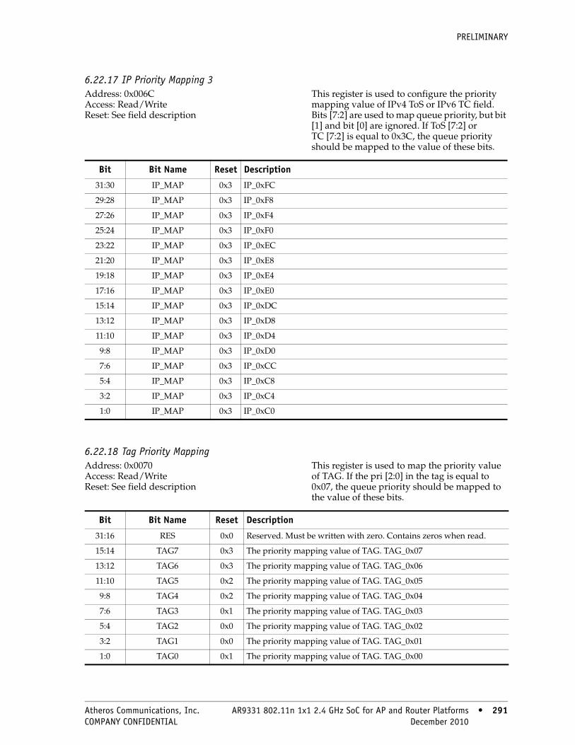
PRELIMINARY
6.22.17 IP Priority Mapping 3Address: 0x006C Access: Read/Write Reset: See field description
This register is used to configure the priority mapping value of IPv4 ToS or IPv6 TC field. Bits [7:2] are used to map queue priority, but bit [1] and bit [0] are ignored. If ToS [7:2] or TC [7:2] is equal to 0x3C, the queue priority should be mapped to the value of these bits.
6.22.18 Tag Priority MappingAddress: 0x0070 Access: Read/Write Reset: See field description
This register is used to map the priority value of TAG. If the pri [2:0] in the tag is equal to 0x07, the queue priority should be mapped to the value of these bits.
Bit Bit Name Reset Description
31:30 IP_MAP 0x3 IP_0xFC
29:28 IP_MAP 0x3 IP_0xF8
27:26 IP_MAP 0x3 IP_0xF4
25:24 IP_MAP 0x3 IP_0xF0
23:22 IP_MAP 0x3 IP_0xEC
21:20 IP_MAP 0x3 IP_0xE8
19:18 IP_MAP 0x3 IP_0xE4
17:16 IP_MAP 0x3 IP_0xE0
15:14 IP_MAP 0x3 IP_0xDC
13:12 IP_MAP 0x3 IP_0xD8
11:10 IP_MAP 0x3 IP_0xD4
9:8 IP_MAP 0x3 IP_0xD0
7:6 IP_MAP 0x3 IP_0xCC
5:4 IP_MAP 0x3 IP_0xC8
3:2 IP_MAP 0x3 IP_0xC4
1:0 IP_MAP 0x3 IP_0xC0
Bit Bit Name Reset Description
31:16 RES 0x0 Reserved. Must be written with zero. Contains zeros when read.
15:14 TAG7 0x3 The priority mapping value of TAG. TAG_0x07
13:12 TAG6 0x3 The priority mapping value of TAG. TAG_0x06
11:10 TAG5 0x2 The priority mapping value of TAG. TAG_0x05
9:8 TAG4 0x2 The priority mapping value of TAG. TAG_0x04
7:6 TAG3 0x1 The priority mapping value of TAG. TAG_0x03
5:4 TAG2 0x0 The priority mapping value of TAG. TAG_0x02
3:2 TAG1 0x0 The priority mapping value of TAG. TAG_0x01
1:0 TAG0 0x1 The priority mapping value of TAG. TAG_0x00
Atheros Communications, Inc. AR9331 802.11n 1x1 2.4 GHz SoC for AP and Router Platforms • 291 COMPANY CONFIDENTIAL December 2010 • 291

PRELIMINARY
6.22.19 Service TagAddress: 0x0074 Access: Read/Write Reset: 0x0
This register is used to double tag egress packets and recognize double tagged packets at ingress.
6.22.20 CPU PortAddress: 0x0078 Access: Read/Write Reset: See field description
This register is used to identify CPU connected ports and mirror ports.
6.22.21 MIB Function0Address: 0x0080 Access: Read/Write Reset: 0x0
This register is used to set the MIB functions such as the auto-cast timer and MIB functions.
Bit Bit Name Description
31:16 RES Reserved. Must be written with zero. Contains zeros when read.
15:0 SERVICE_TAG The service tag. These bits are used to recognize the double tag at ingress and insert the double tag at egress.
Bit Bit Name Reset Description
31:8 RES 0x0 Reserved. Must be written with zero. Contains zeros when read.
7:4 MIRROR_PORT_NUM
0xF Represents the port number to which packets are to be mirrored. 0x0 is port0, 0x1 is port1 and so on. If this value is more than 5, no mirror port is connected to the switch.
3:0 RES 0x0 Reserved. Must be written with zero. Contains zeros when read.
Bit Bit Name Description
31:27 RES Reserved. Must be written with zero. Contains zeros when read.
26:24 MIB_FUNC The current MIB function
000 No Operation
001 Flush all counters on all ports
010 Reserved
011 Capture all counters for all ports and auto-cast to the CPU port
1xx Reserved
23:18 RES Reserved. Must be written with zero. Contains zeros when read.
17 MIB_BUSY The MIB module status
0 The MIB module is currently empty and can access a new command
1 The MIB module is busy and cannot access a new command
16 MIB_AT_HALFEN
The MIB auto-cast is enabled due to half flow. If set to one, the MIB will be auto-cast when the highest bit count for any counter is set as 1.
15:0 MIB_TIMER The MIB auto-cast timer. If set to 0, the MIB will not auto-cast because the timer timed out. This timer is set in periods of 8.4 ms. The recommended value is 0x100. (8.4 ms x 4)
292 • AR9331 802.11n 1x1 2.4 GHz SoC for AP and Router Platforms Atheros Communications, Inc. 292 • December 2010 COMPANY CONFIDENTIAL

PRELIMINARY
6.22.22 MDIO ControlAddress: 0x0098 Access: Read/Write Reset: 0x0
This register is used to control the functions of the MDIO interface.
Bit Bit Name Description
31 MDIO_BUSY Writing a one to this bit represents the internal MDIO interface as busy. This bit should be set when the CPU reads or writes to the PHY register through the internal MDIO interface, and should be cleared after the hardware finishes this command
30 MDIO_ MASTER_EN
Writing a 1 to this bit enables the MDIO master which is used to configure the PHY register. MDC should change to the internal MDC to PHY
29:28 RES Reserved. Must be written with zero. Contains zeros when read.
27 MDIO_CMD This bit represents the commands given for the MDIO
0 Write
1 Read
26 MDIO_SUP_ PRE Writing a 1 to this bit enables the supposed preamble
25:21 PHY_ADDR These bits represent the PHY address
20:16 REG_ADDR These bits represent the PHY register address
15:0 MDIO_DATA When write, these bits are data written to the PHY register. When read, these bits are read out from the PHY register
Atheros Communications, Inc. AR9331 802.11n 1x1 2.4 GHz SoC for AP and Router Platforms • 293 COMPANY CONFIDENTIAL December 2010 • 293
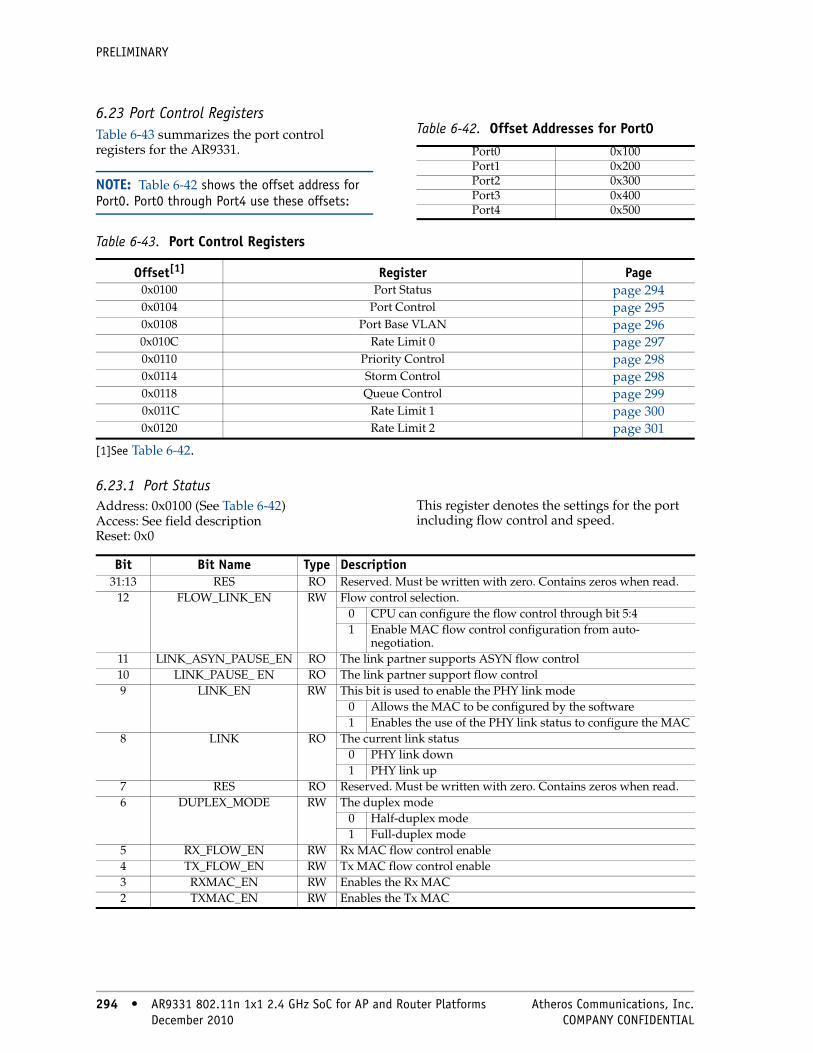
PRELIMINARY
6.23 Port Control RegistersTable 6-43 summarizes the port control registers for the AR9331.
6.23.1 Port StatusAddress: 0x0100 (See Table 6-42) Access: See field description Reset: 0x0
This register denotes the settings for the port including flow control and speed.
NOTE: Table 6-42 shows the offset address for Port0. Port0 through Port4 use these offsets:
Table 6-42. Offset Addresses for Port0Port0 0x100Port1 0x200Port2 0x300Port3 0x400Port4 0x500
Table 6-43. Port Control Registers
Offset[1] Register Page0x0100 Port Status page 2940x0104 Port Control page 2950x0108 Port Base VLAN page 2960x010C Rate Limit 0 page 2970x0110 Priority Control page 2980x0114 Storm Control page 2980x0118 Queue Control page 299 0x011C Rate Limit 1 page 3000x0120 Rate Limit 2 page 301
[1]See Table 6-42.
Bit Bit Name Type Description31:13 RES RO Reserved. Must be written with zero. Contains zeros when read.
12 FLOW_LINK_EN RW Flow control selection.0 CPU can configure the flow control through bit 5:41 Enable MAC flow control configuration from auto-
negotiation.11 LINK_ASYN_PAUSE_EN RO The link partner supports ASYN flow control10 LINK_PAUSE_ EN RO The link partner support flow control9 LINK_EN RW This bit is used to enable the PHY link mode
0 Allows the MAC to be configured by the software1 Enables the use of the PHY link status to configure the MAC
8 LINK RO The current link status0 PHY link down1 PHY link up
7 RES RO Reserved. Must be written with zero. Contains zeros when read.6 DUPLEX_MODE RW The duplex mode
0 Half-duplex mode1 Full-duplex mode
5 RX_FLOW_EN RW Rx MAC flow control enable4 TX_FLOW_EN RW Tx MAC flow control enable3 RXMAC_EN RW Enables the Rx MAC2 TXMAC_EN RW Enables the Tx MAC
294 • AR9331 802.11n 1x1 2.4 GHz SoC for AP and Router Platforms Atheros Communications, Inc. 294 • December 2010 COMPANY CONFIDENTIAL
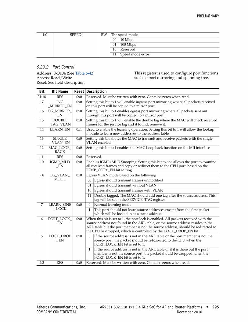
PRELIMINARY
6.23.2 Port ControlAddress: 0x0104 (See Table 6-42) Access: Read/Write Reset: See field description
This register is used to configure port functions such as port mirroring and spanning tree.
1:0 SPEED RW The speed mode00 10 Mbps01 100 Mbps10 Reserved11 Speed mode error
Bit Bit Name Reset Description31:18 RES 0x0 Reserved. Must be written with zero. Contains zeros when read.
17 ING_MIRROR_EN
0x0 Setting this bit to 1 will enable ingress port mirroring where all packets received on this port will be copied to a mirror port
16 EG_MIRROR_EN
0x0 Setting this bit to 1 enables egress port mirroring where all packets sent out through this port will be copied to a mirror port
15 DOUBLE_TAG_VLAN
0x0 Setting this bit to 1 will enable the double tag where the MAC will check received frames for the service tag and if found, remove it.
14 LEARN_EN 0x1 Used to enable the learning operation. Setting this bit to 1 will allow the lookup module to learn new addresses to the address table
13 SINGLE_VLAN_EN
0x0 Setting this bit allows the MAC to transmit and receive packets with the single VLAN enabled
12 MAC_LOOP_ BACK
0x0 Setting this bit to 1 enables the MAC Loop back function on the MII interface
11 RES 0x0 Reserved.10 IGMP_MLD
_EN0x0 Enables IGMP/MLD Snooping. Setting this bit to one allows the port to examine
all received frames and copy or redirect them to the CPU port, based on the IGMP_COPY_EN bit setting.
9:8 EG_VLAN_ MODE
0x0 Egress VLAN mode based on the following00 Egress should transmit frames unmodified01 Egress should transmit without VLAN10 Egress should transmit frames with VLAN11 Double tagged. The MAC should add one tag after the source address. This
tag will be set in the SERVICE_TAG register7 LEARN_ONE
_ LOCK0x0 0 Normal learning mode
1 This port should not learn source addresses except from the first packet which will be locked in as a static address
6 PORT_LOCK_EN
0x0 When this bit is set to 1, the port lock is enabled. All packets received with the source address not found in the ARL table, or the source address resides in the ARL table but the port member is not the source address, should be redirected to the CPU or dropped, which is controlled by the LOCK_DROP_EN bit.
5 LOCK_DROP_ EN
0x0 0 If the source address is not in the ARL table or the port member is not the source port, the packet should be re4directed to the CPU when the PORT_LOCK_EN bit is set to 1.
1 If the source address is not in the ARL table or if it is there but the port member is not the source port, the packet should be dropped when the PORT_LOCK_EN bit is set to 1.
4:3 RES 0x0 Reserved. Must be written with zero. Contains zeros when read.
Atheros Communications, Inc. AR9331 802.11n 1x1 2.4 GHz SoC for AP and Router Platforms • 295 COMPANY CONFIDENTIAL December 2010 • 295

PRELIMINARY
6.23.3 Port Base VLANAddress: 0x0108 (See Table 6-42) Access: Read/Write Reset: 0x0
This register is used to configure the bits for the VLANs, including port VIDs and Leaky VLANs.
2:0 PORT_STATE 0x4 Port state. These bits manage the port to determine what kind of frames may enter or leave the port for simple bridge loop detection or 803.1D Spanning Tree.000 Disabled mode: port cannot send or receive frames001 Blocking mode: port forwards Rx management frames to the designed port
only. Other frames are not transmitted or received and do not learn source addresses.
010 Listening mode: port receives and transmits only management frames without learning the source address. Other frames are not transmitted or received.
011 Learning mode: port learns all source addresses and discards all frames except management frames, which can only be transmitted.
100 Forwarding mode: port learns all source addresses and transmit and receive frames normally.
Bit Bit Name Description31:30 8021Q_MODE Sets the 802.1Q mode for this port
00 Disables the 802.1Q VLAN function. Port-based VLAN used only.
01 Enables 802.1Q for all received frames. If the VID for the received frame is not contained in the VLAN table, port VLANs will be used and ingress membership will not be discarded.
10 Enables 802.1Q for all received frames. Frames will be discarded only if the VID of the frames are not contained in the VLAN table. Ingress membership will not be discarded.
11 Enables 802.1Q for all received frames. Frames will be discarded if the VID of the frames are not contained in the VLAN table and ingress membership will be discarded.
29:27 ING_PORT_PRI The port default priority for received frames.
26 FORCE_PORT_ VLAN_EN
Setting this bit forces port-based VLANs to be enabled. This uses the port base VLAN and the VLAN table to determine the destination port.
25:16 PORT_VID_ MEMBER
Port Base VLAN Member. Each bit restricts which port can send frames to, for port 0, bit 16 must be set to 1, for port 1, bit 17 must be set to 1, etc. These bits are set to one after reset except the port’s bit. This prevents frames going out from the port they are received.
15 ARP_LEAKY_EN Setting this bit to 1 allows received frames from this port on the MAC to cross all VLANs (both port-based and 802.1Q)
14 UNI_LEAKY_EN Used to enable Unicast frames for the leaky VLAN. If the MAC receives unicast frames on this port, it should forward them as leaky VLAN frames. These frames may be switched to the destination port defined in the ARL table and then across all VLANs (including port-based and 802.1Q).Users may enable the ARL_MULTI_LEAKY_EN bit and the LEAKY_EN bit the ARL table to control unicast frames for the leaky VLAN.When the ARL_MULTI_LEAKY_EN is set to 0, only the MULTI_LEAKY_EN controls multicast frames for the leaky VLAN.If the ARL_MULTI_LEAKY_VLAN bit is set to 1, only frames with the destination address in the ARL table and their LEAKY_EN bit is set to 1, can be forwarded as leaky VLAN frames. This will force the MULTI_LEAKY_EN bit to be ignored.
296 • AR9331 802.11n 1x1 2.4 GHz SoC for AP and Router Platforms Atheros Communications, Inc. 296 • December 2010 COMPANY CONFIDENTIAL
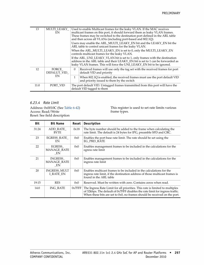
PRELIMINARY
6.23.4 Rate LimitAddress: 0x0010C (See Table 6-42) Access: Read/Write Reset: See field description
This register is used to set rate limits various frame types.
13 MULTI_LEAKY_EN
Used to enable Multicast frames for the leaky VLAN. If the MAC receives multicast frames on this port, it should forward them as leaky VLAN frames. These frames may be switched to the destination port defined in the ARL table and then across all VLANs (including port-based and 802.1Q).Users may enable the ARL_MULTI_LEAKY_EN bit and the LEAKY_EN bit the ARL table to control unicast frames for the leaky VLAN.When the ARL_MULTI_LEAKY_EN is set to 0, only the MULTI_LEAKY_EN controls multicast frames for the leaky VLAN.If the ARL_UNI_LEAKY_VLAN bit is set to 1, only frames with the destination address in the ARL table and their LEAKY_EN bit is set to 1 can be forwarded as leaky VLAN frames. This will force the UNI_LEAKY_EN bit to be ignored.
12 FORCE_ DEFALUT_VID_
EN
0 Received frames will use only the tag set with the received frames for port default VID and priority
1 When 802.1Q is enabled, the received frames must use the port default VID and priority issued to them by the switch
11:0 PORT_VID The port default VID. Untagged frames transmitted from this port will have the default VID tagged to them
Bit Bit Name Reset Description
31:24 ADD_RATE_ BYTE
0x18 The byte number should be added to the frame when calculating the rate limit. The default is 24 bytes for IPG, preamble SFD and CRC.
23 EGRESS_RATE_ EN
0x0 Enables the port base rate limit. The rate should be set using the EG_PRI3_RATE
22 EGRESS_ MANAGE_RATE
_EN
0x0 Enables management frames to be included in the calculations for the egress rate limit
21 INGRESS_ MANAGE_RATE
_EN
0x0 Enables management frames to be included in the calculations for the ingress rate limit
20 INGRESS_MULTI_RATE_EN
0x0 Enables multicast frames to be included in the calculations for the ingress rate limit, if the destination address of those multicast frames is found in the ARL table
19:15 RES 0x0 Reserved. Must be written with zero. Contains zeros when read.
14:0 ING_RATE 0x7FFF The Ingress Rate Limit for all priorities. This rate is limited to multiples of 32kbps. The default of 0x7FFF disables the rate limit for ingress traffic. When these bits are set to 0x0, no frames should be received on the port.
Atheros Communications, Inc. AR9331 802.11n 1x1 2.4 GHz SoC for AP and Router Platforms • 297 COMPANY CONFIDENTIAL December 2010 • 297
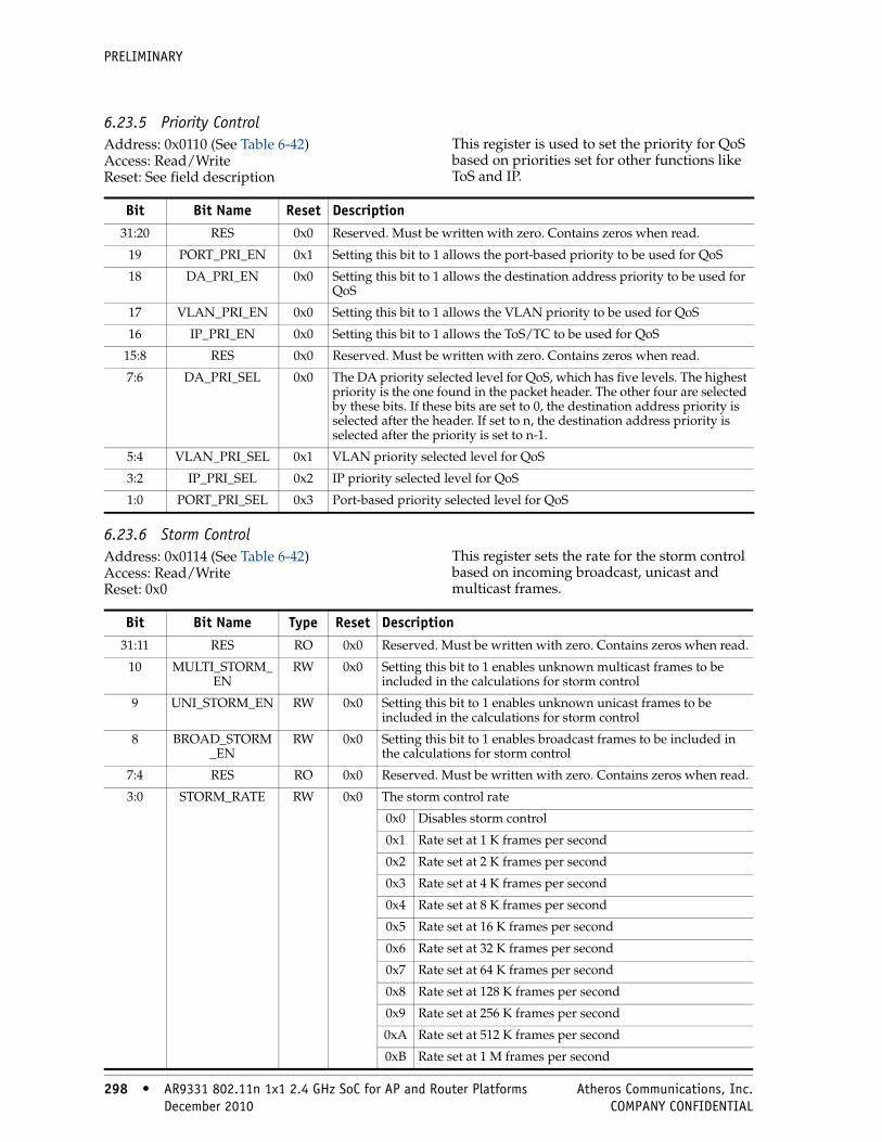
PRELIMINARY
6.23.5 Priority ControlAddress: 0x0110 (See Table 6-42) Access: Read/Write Reset: See field description
This register is used to set the priority for QoS based on priorities set for other functions like ToS and IP.
6.23.6 Storm ControlAddress: 0x0114 (See Table 6-42) Access: Read/Write Reset: 0x0
This register sets the rate for the storm control based on incoming broadcast, unicast and multicast frames.
Bit Bit Name Reset Description31:20 RES 0x0 Reserved. Must be written with zero. Contains zeros when read.
19 PORT_PRI_EN 0x1 Setting this bit to 1 allows the port-based priority to be used for QoS
18 DA_PRI_EN 0x0 Setting this bit to 1 allows the destination address priority to be used for QoS
17 VLAN_PRI_EN 0x0 Setting this bit to 1 allows the VLAN priority to be used for QoS
16 IP_PRI_EN 0x0 Setting this bit to 1 allows the ToS/TC to be used for QoS
15:8 RES 0x0 Reserved. Must be written with zero. Contains zeros when read.
7:6 DA_PRI_SEL 0x0 The DA priority selected level for QoS, which has five levels. The highest priority is the one found in the packet header. The other four are selected by these bits. If these bits are set to 0, the destination address priority is selected after the header. If set to n, the destination address priority is selected after the priority is set to n-1.
5:4 VLAN_PRI_SEL 0x1 VLAN priority selected level for QoS
3:2 IP_PRI_SEL 0x2 IP priority selected level for QoS
1:0 PORT_PRI_SEL 0x3 Port-based priority selected level for QoS
Bit Bit Name Type Reset Description31:11 RES RO 0x0 Reserved. Must be written with zero. Contains zeros when read.
10 MULTI_STORM_EN
RW 0x0 Setting this bit to 1 enables unknown multicast frames to be included in the calculations for storm control
9 UNI_STORM_EN RW 0x0 Setting this bit to 1 enables unknown unicast frames to be included in the calculations for storm control
8 BROAD_STORM_EN
RW 0x0 Setting this bit to 1 enables broadcast frames to be included in the calculations for storm control
7:4 RES RO 0x0 Reserved. Must be written with zero. Contains zeros when read.
3:0 STORM_RATE RW 0x0 The storm control rate
0x0 Disables storm control
0x1 Rate set at 1 K frames per second
0x2 Rate set at 2 K frames per second
0x3 Rate set at 4 K frames per second
0x4 Rate set at 8 K frames per second
0x5 Rate set at 16 K frames per second
0x6 Rate set at 32 K frames per second
0x7 Rate set at 64 K frames per second
0x8 Rate set at 128 K frames per second
0x9 Rate set at 256 K frames per second
0xA Rate set at 512 K frames per second
0xB Rate set at 1 M frames per second
298 • AR9331 802.11n 1x1 2.4 GHz SoC for AP and Router Platforms Atheros Communications, Inc. 298 • December 2010 COMPANY CONFIDENTIAL

PRELIMINARY
6.23.7 Queue ControlAddress: 0x0118 (See Table 6-42) Access: Read/Write Reset: See field description
This register is used to set the buffer controls for QoS queues.
Bit Bit Name Reset Description31:26 RES 0x0 Reserved. Must be written with zero. Contains zeros when read.
25 PORT_QUEUE_CTRL_EN
0x1 Setting this bit to 1 enables the specified port to use the memory depth control feature
24 PRI_QUEUE_ CTRL_EN
0x0 Setting this bit to 1 enables the memory depth control for this port based on priority
23:21 RES 0x0 Reserved. Must be written with zero. Contains zeros when read.
20:16 PRI_QUEUE_ NUM 0x10 This field sets the limit of the buffer size for QoS priority queue. Each bit represents a block of memory x 4, where each block represents 256 bytes. Therefore the maximum amount of memory that this bit can hold in the queue is 1024 bytes. (4x 256 = 1024)
0x0 No memory for the queue
0x1 A maximum of 4 blocks (1024 bytes)
0x2 A maximum of 8 blocks (2048 bytes)
0x3 A maximum of 12 blocks (3072 bytes)
... ...
0x1F A maximum of 120 blocks (30720 bytes)
Each successive hex value holds the same formula until 0x1F which will be a maximum of 120 blocks (30720 bytes)
15:12 PRI3_QUEUE_ NUM 0x0 This field sets the limit of the buffer size for QoS priority queue 3. Each bit represents a block of memory x 4, where each block represents 256 bytes. Therefore the maximum amount of memory that this bit can hold in the queue is 1024 bytes. (4x 256 = 1024)
0x0 No memory for the queue
0x1 A maximum of 4 blocks (1024 bytes)
0x2 A maximum of 8 blocks (2048 bytes)
0x3 A maximum of 12 blocks (3072 bytes)
... ...
0xF A maximum of 60 blocks (15360 bytes)
Each successive hex value holds the same formula until 0xF which will be a maximum of 60 blocks (15360 bytes)
11:8 PRI2_QUEUE_ NUM 0x0 This field sets the limit of the buffer size for QoS priority queue 2. Each bit represents a block of memory x 4, where each block represents 256 bytes. Therefore the maximum amount of memory that this bit can hold in the queue is 1024 bytes. (4x 256 = 1024)
0x0 No memory for the queue
0x1 A maximum of 4 blocks (1024 bytes)
0x2 A maximum of 8 blocks (2048 bytes)
0x3 A maximum of 12 blocks (3072 bytes)
... ...
0xF A maximum of 60 blocks (15360 bytes)
Each successive hex value holds the same formula until 0xF which will be a maximum of 60 blocks (15360 bytes)
Atheros Communications, Inc. AR9331 802.11n 1x1 2.4 GHz SoC for AP and Router Platforms • 299 COMPANY CONFIDENTIAL December 2010 • 299

PRELIMINARY
6.23.8 Rate Limit Register 1Address: 0x011C (See Table 6-42) Access: Read/Write Reset: See field description
This register is used to set the rate limits for priority queues.
7:4 PRI1_QUEUE_ NUM 0x0 This field sets the limit of the buffer size for QoS priority queue 1. Each bit represents a block of memory x 4, where each block represents 256 bytes. Therefore the maximum amount of memory that this bit can hold in the queue is 1024 bytes. (4x 256 = 1024)
0x0 No memory for the queue
0x1 A maximum of 4 blocks (1024 bytes)
0x2 A maximum of 8 blocks (2048 bytes)
0x3 A maximum of 12 blocks (3072 bytes)
... ...
0xF A maximum of 60 blocks (15360 bytes)
Each successive hex value holds the same formula until 0xF which will be a maximum of 60 blocks (15360 bytes)
3:0 PRI0_QUEUE_ NUM 0x0 This field sets the limit of the buffer size for QoS priority queue 0. Each bit represents a block of memory x 4, where each block represents 256 bytes. Therefore the maximum amount of memory that this bit can hold in the queue is 1024 bytes. (4x 256 = 1024)
0x0 No memory for the queue
0x1 A maximum of 4 blocks (1024 bytes)
0x2 A maximum of 8 blocks (2048 bytes)
0x3 A maximum of 12 blocks (3072 bytes)
... ...
0xF A maximum of 60 blocks (15360 bytes)
Each successive hex value holds the same formula until 0xF which will be a maximum of 60 blocks (15360 bytes)
Bit Bit Name Reset Description
31 RES 0x0 Reserved. Must be written with zero. Contains zeros when read.
30:16 EG_PRI1_RATE 0x7FFF The egress rate limit for priority 1. The rate limit is calculated in increments of 32 Kbps. The reset value will disable the rate limit for egress priority 2. If these bits are set to 0 no priority 1 frame will be sent out from this port.
15 RES 0x0 Reserved. Must be written with zero. Contains zeros when read.
14:0 EG_PRI0_RATE 0x7FFF The egress rate limit for priority 0. The rate limit is calculated in increments of 32 Kbps. The reset value will disable the rate limit for egress priority 2. If these bits are set to 0 no priority 0 frame will be sent out from this port.
300 • AR9331 802.11n 1x1 2.4 GHz SoC for AP and Router Platforms Atheros Communications, Inc. 300 • December 2010 COMPANY CONFIDENTIAL
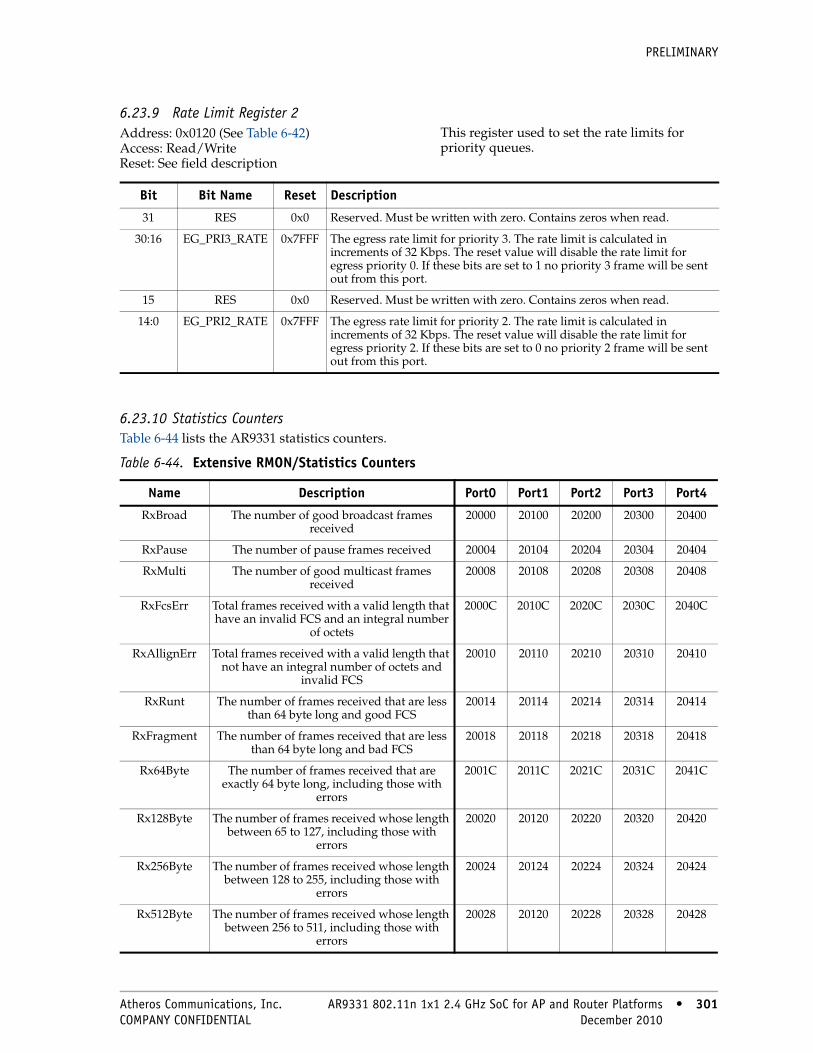
PRELIMINARY
6.23.9 Rate Limit Register 2Address: 0x0120 (See Table 6-42) Access: Read/Write Reset: See field description
This register used to set the rate limits for priority queues.
6.23.10 Statistics CountersTable 6-44 lists the AR9331 statistics counters.
Bit Bit Name Reset Description
31 RES 0x0 Reserved. Must be written with zero. Contains zeros when read.
30:16 EG_PRI3_RATE 0x7FFF The egress rate limit for priority 3. The rate limit is calculated in increments of 32 Kbps. The reset value will disable the rate limit for egress priority 0. If these bits are set to 1 no priority 3 frame will be sent out from this port.
15 RES 0x0 Reserved. Must be written with zero. Contains zeros when read.
14:0 EG_PRI2_RATE 0x7FFF The egress rate limit for priority 2. The rate limit is calculated in increments of 32 Kbps. The reset value will disable the rate limit for egress priority 2. If these bits are set to 0 no priority 2 frame will be sent out from this port.
Table 6-44. Extensive RMON/Statistics Counters
Name Description Port0 Port1 Port2 Port3 Port4
RxBroad The number of good broadcast frames received
20000 20100 20200 20300 20400
RxPause The number of pause frames received 20004 20104 20204 20304 20404
RxMulti The number of good multicast frames received
20008 20108 20208 20308 20408
RxFcsErr Total frames received with a valid length that have an invalid FCS and an integral number
of octets
2000C 2010C 2020C 2030C 2040C
RxAllignErr Total frames received with a valid length that not have an integral number of octets and
invalid FCS
20010 20110 20210 20310 20410
RxRunt The number of frames received that are less than 64 byte long and good FCS
20014 20114 20214 20314 20414
RxFragment The number of frames received that are less than 64 byte long and bad FCS
20018 20118 20218 20318 20418
Rx64Byte The number of frames received that are exactly 64 byte long, including those with
errors
2001C 2011C 2021C 2031C 2041C
Rx128Byte The number of frames received whose length between 65 to 127, including those with
errors
20020 20120 20220 20320 20420
Rx256Byte The number of frames received whose length between 128 to 255, including those with
errors
20024 20124 20224 20324 20424
Rx512Byte The number of frames received whose length between 256 to 511, including those with
errors
20028 20120 20228 20328 20428
Atheros Communications, Inc. AR9331 802.11n 1x1 2.4 GHz SoC for AP and Router Platforms • 301 COMPANY CONFIDENTIAL December 2010 • 301
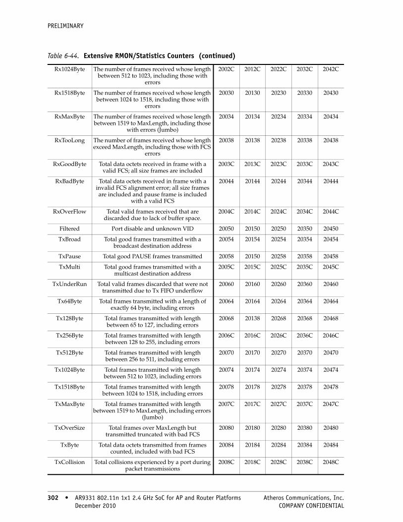
PRELIMINARY
Rx1024Byte The number of frames received whose length between 512 to 1023, including those with
errors
2002C 2012C 2022C 2032C 2042C
Rx1518Byte The number of frames received whose length between 1024 to 1518, including those with
errors
20030 20130 20230 20330 20430
RxMaxByte The number of frames received whose length between 1519 to MaxLength, including those
with errors (Jumbo)
20034 20134 20234 20334 20434
RxTooLong The number of frames received whose length exceed MaxLength, including those with FCS
errors
20038 20138 20238 20338 20438
RxGoodByte Total data octets received in frame with a valid FCS; all size frames are included
2003C 2013C 2023C 2033C 2043C
RxBadByte Total data octets received in frame with a invalid FCS alignment error; all size frames are included and pause frame is included
with a valid FCS
20044 20144 20244 20344 20444
RxOverFlow Total valid frames received that are discarded due to lack of buffer space.
2004C 2014C 2024C 2034C 2044C
Filtered Port disable and unknown VID 20050 20150 20250 20350 20450
TxBroad Total good frames transmitted with a broadcast destination address
20054 20154 20254 20354 20454
TxPause Total good PAUSE frames transmitted 20058 20150 20258 20358 20458
TxMulti Total good frames transmitted with a multicast destination address
2005C 2015C 2025C 2035C 2045C
TxUnderRun Total valid frames discarded that were not transmitted due to Tx FIFO underflow
20060 20160 20260 20360 20460
Tx64Byte Total frames transmitted with a length of exactly 64 byte, including errors
20064 20164 20264 20364 20464
Tx128Byte Total frames transmitted with length between 65 to 127, including errors
20068 20138 20268 20368 20468
Tx256Byte Total frames transmitted with length between 128 to 255, including errors
2006C 2016C 2026C 2036C 2046C
Tx512Byte Total frames transmitted with length between 256 to 511, including errors
20070 20170 20270 20370 20470
Tx1024Byte Total frames transmitted with length between 512 to 1023, including errors
20074 20174 20274 20374 20474
Tx1518Byte Total frames transmitted with length between 1024 to 1518, including errors
20078 20178 20278 20378 20478
TxMaxByte Total frames transmitted with length between 1519 to MaxLength, including errors
(Jumbo)
2007C 2017C 2027C 2037C 2047C
TxOverSize Total frames over MaxLength but transmitted truncated with bad FCS
20080 20180 20280 20380 20480
TxByte Total data octets transmitted from frames counted, included with bad FCS
20084 20184 20284 20384 20484
TxCollision Total collisions experienced by a port during packet transmissions
2008C 2018C 2028C 2038C 2048C
Table 6-44. Extensive RMON/Statistics Counters (continued)
302 • AR9331 802.11n 1x1 2.4 GHz SoC for AP and Router Platforms Atheros Communications, Inc. 302 • December 2010 COMPANY CONFIDENTIAL
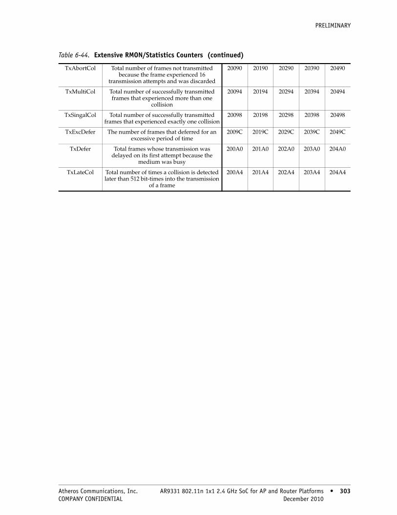
PRELIMINARY
TxAbortCol Total number of frames not transmitted because the frame experienced 16
transmission attempts and was discarded
20090 20190 20290 20390 20490
TxMultiCol Total number of successfully transmitted frames that experienced more than one
collision
20094 20194 20294 20394 20494
TxSingalCol Total number of successfully transmitted frames that experienced exactly one collision
20098 20198 20298 20398 20498
TxExcDefer The number of frames that deferred for an excessive period of time
2009C 2019C 2029C 2039C 2049C
TxDefer Total frames whose transmission was delayed on its first attempt because the
medium was busy
200A0 201A0 202A0 203A0 204A0
TxLateCol Total number of times a collision is detected later than 512 bit-times into the transmission
of a frame
200A4 201A4 202A4 203A4 204A4
Table 6-44. Extensive RMON/Statistics Counters (continued)
Atheros Communications, Inc. AR9331 802.11n 1x1 2.4 GHz SoC for AP and Router Platforms • 303 COMPANY CONFIDENTIAL December 2010 • 303

PRELIMINARY
304 • AR9331 802.11n 1x1 2.4 GHz SoC for AP and Router Platforms Atheros Communications, Inc. 304 • December 2010 COMPANY CONFIDENTIAL

PRELIMINARY
7. Electrical Characteristics
7.1 Absolute Maximum RatingsTable 7-1 summarizes the absolute maximum ratings and Table 7-2 lists the recommended operating conditions for the AR9331. Absolute maximum ratings are those values beyond which damage to the device can occur.
Functional operation under these conditions, or at any other condition beyond those indicated in the operational sections of this document, is not recommended.
7.2 Recommended Operating Conditions
Table 7-1. Absolute Maximum Ratings
Symbol Parameter Max Rating Unit
Vdd12 Supply Voltage –0.3 to 1.8 V
Vdd33 Maximum I/O Supply Voltage –0.3 to 4.0 V
Tstore Storage Temperature –65 to 150 °C
Tj Junction Temperature 125 °C
ESD Electrostatic Discharge Tolerance 2000 V
Electrostatic Discharge Tolerance (LDO_OUT) TBD V
Electrostatic Discharge Tolerance (USB_DP, USB_DM) TBD V
Table 7-2. Recommended Operating Conditions
Symbol Parameter Conditions Min Typ Max Unit
VDD33 Supply Voltage ± 10% 2.97 3.3 3.63 V
VDD25 I/O Supply Voltage ± 10% 2.25 2.5 2.75 V
VDD12 Core Supply Voltage ± 5% 1.14 1.2 1.26 V
AVDD20 Voltage for Ethernet PHY — 1.9 2.0 2.15 V
VDD_DDR[1] DDR1 I/O Voltage (2.6 V) ± 5% 2.47 2.6 2.73 V
DDR2 I/O Voltage (1.8 V) ± 5% 1.71 1.8 1.89 V
SDRAM I/O Voltage (3.0 V) ± 5% 2.85 3.0 3.15 V
Tcase Commercial Case Temperature — 0 — 110 °C
PsiJT Thermal Parameter[2] — — — 2.2 °C/W
[1]VDD_DDR voltage is configured by the boot strap setting.[2]For 12x12 dual-row LPCC package.
Atheros Communications, Inc. AR9331 802.11n 1x1 2.4 GHz SoC for AP and Router Platforms • 305 COMPANY CONFIDENTIAL December 2010 • 305
PRELIMINARY
7.3 25/40 MHz Clock CharacteristicsWhen using an external clock, the XTALI pin is grounded and the XTALO pin should be driven with a square wave clock.
AC coupling is recommended for the clock signal to the XTALO pin.
The internal circuit provides the DC bias of approximately 0.6 V. The peak-to-peak swing of the external clock can be between 0.6 V to 1.2 V. Larger swings and sharper edges will reduce jitter.
7.4 GPIO CharacteristicsTable 7-4 and Table 7-5 define the input and output characteristics of the GPIO pins for the AR9331. This table already takes into account the VDD25 tolerance which originates from
LDO25_OUT which has an output voltage of 2.62 V ± 5%.
Table 7-3. 25/40 Clock Square Wave Characteristics
Symbol Parameter Conditions Min Typ Max Unit
VIH Input High Voltage — 0.9 — 1.4 V
VIL Input Low Voltage[1] — -0.2 — 0.2 V
TDCycle Duty Cycle — 40 50 60 %
TRise Rise Time — — — 2 ns
TFall Fall Time — — — 2 ns
[1]VIL of -0.2 V is limited by the ESD protection diode. If VIL is less than -0.2 V, the ESD diode turns on and protects the chip. However, VIL can go as low as -0.7 V without damage so long as the DC current sourced by the pin is limited by an AC coupling capacitor.
Table 7-4. General GPIO Characteristics
Symbol Parameter Conditions Min Typ Max Unit
VOH Output High Voltage — 2.44 — — V
VOL Output Low Voltage — — — 0.1 V
VIH Input High Voltage — 0.7 — — V
VIL Input Low Voltage — 0.3 — — ns
Table 7-5. GPIO Characteristics
Signal Name Pin Type Drive PU/PD Resistance
GPIO_0 – GPIO_28 A27, A29, A28, A52, A54, A56, A57, A75, A76, A77, A78, A79, B23, B22, B24, B25,
B46, B48, B49, B50, B51, B64, B65, B66, B68
I/O Up to 24 mA 200 KΩ
306 • AR9331 802.11n 1x1 2.4 GHz SoC for AP and Router Platforms Atheros Communications, Inc. 306 • December 2010 COMPANY CONFIDENTIAL
PRELIMINARY
7.5 Power On SequenceThe AR9331 has an internal power on circuit reset. when all power inputs, including VDD33, VDD12 and VDD25, are ready, the RESET_L signal; will be released from low to high. This signal is connected to a digital counter which controls the digital reset and is released after 5 μs. When the digital reset goes
from low to high, the CPU begins fetching instructions from the internal ROM or the external SPI in order to boot the system. Figure 7-1 better describes the power on sequencing for the AR9331
Figure 7-1. Power on sequencing for the AR9331
VDD33
RESET_L
Digital reset(internal signal)
5ms
Atheros Communications, Inc. AR9331 802.11n 1x1 2.4 GHz SoC for AP and Router Platforms • 307 COMPANY CONFIDENTIAL December 2010 • 307
PRELIMINARY
7.6 SPI Flash TimingFigure 7-2 depicts the SPI Flash timing for the AR9331.
Figure 7-2. SPI Flash Timing
Table 7-6 denotes the timing, in nanoseconds, for the SPI Flash.
SPI_CK
SPI_DO
tdrdy
tck
tdhtds
SPI_DI
SPI_CS
tcsv
tcsv
Table 7-6. SPI Flash Timing per signal
Signal Name Description Min (ns) Max (ns)
TCK SPI_CK_P pin period 20 —
TCSV SPI_CS valid time after SPI_CK falling edge 0 3.0
TDH SPI_DI hold time after SPI_DI rising edge — 5.0
TDSU SPI_DI setup time before SPI_CK rising edge — 5.0
TDRDY SPI_DO data delay time after SPI_CK falling edge 5.0 0
308 • AR9331 802.11n 1x1 2.4 GHz SoC for AP and Router Platforms Atheros Communications, Inc. 308 • December 2010 COMPANY CONFIDENTIAL

PRELIMINARY
7.7 DDR Output TimingFigure 7-3 depicts the DDR output timing for the AR9331.
Figure 7-3. AR9331 Output timing
Table 7-7 details the output timing of the Data, Address and Control signals.
CK_P
DQS
Data
Address/Control
tdqsd
tdrdy
tch
tck
tdh
tcrdy
Table 7-7. Data, address and control signals output timing
Signal Name Description Min (ns) Max (ns)
TCK CK_P pin period 2.5 —
TDSQSD DQS delay time after CK_P rising edge -0.3 0.2
TDH Data hold time after DQS edge 0.4 1.3
TDRDY Data ready time after DQS edge 0.5 1.6
TCH Control/address hold time after CK_P edge 0.5 1.3
TCRDY Control/address ready time after CK_P edge 0.4 1.5
Atheros Communications, Inc. AR9331 802.11n 1x1 2.4 GHz SoC for AP and Router Platforms • 309 COMPANY CONFIDENTIAL December 2010 • 309
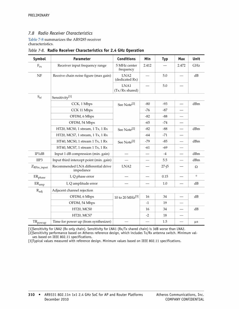
PRELIMINARY
7.8 Radio Receiver CharacteristicsTable 7-8 summarizes the AR9285 receiver characteristics.
Table 7-8. Radio Receiver Characteristics for 2.4 GHz Operation
Symbol Parameter Conditions Min Typ Max Unit
Frx Receiver input frequency range 5 MHz center frequency
2.412 — 2.472 GHz
NF Receive chain noise figure (max gain) LNA2 (dedicated Rx)
— 5.0 — dB
LNA1 (Tx/Rx shared)
— 5.0 —
Srf Sensitivity[1]
CCK, 1 Mbps See Note[2] -80 -93 — dBm
CCK 11 Mbps -76 -87 —
OFDM, 6 Mbps -82 -88 —
OFDM, 54 Mbps -65 -74 —
HT20, MCS0, 1 stream, 1 Tx, 1 Rx See Note[2] -82 -88 — dBm
HT20, MCS7, 1 stream, 1 Tx, 1 Rx -64 -71 —
HT40, MCS0, 1 stream 1 Tx, 1 Rx See Note[2] -79 -85 — dBm
HT40, MCS7, 1 stream 1 Tx, 1 Rx -61 -69 —
IP1dB Input 1 dB compression (min. gain) — — -4 — dBm
IIP3 Input third intercept point (min. gain) — — 5.5 — dBm
ZRFin_input Recommended LNA differential drive impedance
LNA2 — 27-j5 — Ω
ERphase I, Q phase error — — 0.15 — °
ERamp I, Q amplitude error — — 1.0 — dB
Radj Adjacent channel rejection
OFDM, 6 Mbps 10 to 20 MHz[3] 16 34 — dB
OFDM, 54 Mbps -1 19 —
HT20, MCS0 16 34 — dB
HT20, MCS7 -2 18 —
TRpowup Time for power up (from synthesizer) — — 1.5 — μs
[1]Sensitivity for LNA2 (Rx only chain). Sensitivity for LNA1 (Rx/Tx shared chain) is 3dB worse than LNA2.[2]Sensitivity performance based on Atheros reference design, which includes Tx/Rx antenna switch. Minimum val-
ues based on IEEE 802.11 specifications.[3]Typical values measured with reference design. Minimum values based on IEEE 802.11 specifications.
310 • AR9331 802.11n 1x1 2.4 GHz SoC for AP and Router Platforms Atheros Communications, Inc. 310 • December 2010 COMPANY CONFIDENTIAL

PRELIMINARY
7.9 Radio Transmitter CharacteristicsTable 7-9 summarizes the transmitter characteristics of the AR9285.
Table 7-9. Transmitter Characteristics for 2.4 GHz Operation
Symbol Parameter Conditions Min Typ Max UnitFtx Transmit output frequency range 5 MHz center
frequency2.412 — 2.472 GHz
Pout Mask Compliant CCK output power See Note[1] — 19.5 — dBm
Mask Compliant OFDM output power
802.11g BPSK 6 Mbps See Note[2] — 20 — dBm
HT20, MCS0 — 19 —
HT40, MCS0 — 16 —
EVM Compliant OFDM output power
802.11g 64 QAM 54 Mbps See Note[1] — 19 —
HT20, MCS7 — 17 — dBm
HT40, MCS7 — 16 —
SPgain PA gain step See Note[2] — 0.5 — dB
Apl Accuracy of power leveling loop See Notes[3][4] — ±0.5 — dB
ZRFout_load Recommend differential PA load impedance
See Note[5] — 12+j13 — Ω
OP1dB Output P1dB (max. gain) 2.442 GHz — 21 — dBm
OIP3 Output third order intercept point (max. gain)
2.442 GHz — 31 — dBm
SS Sideband suppression — — –37 — dBc
RS Synthesizer reference spur — — –62 — dBc
TTpowup Time for power up (from synthesizer on) — — 1.5 — μs
[1]Measured using the balun recommended by Atheros under Tx power control.[2]Guaranteed by design.[3]Manufacturing calibration required.[4]Not including tolerance of external power detector and its temperature variation.[5]See the impedance matching circuit in the Atheros reference design schematics. To achieve good RF performance,
it is strongly recommended not to alter the RF portion of the Atheros reference design for different matching networks.
Atheros Communications, Inc. AR9331 802.11n 1x1 2.4 GHz SoC for AP and Router Platforms • 311 COMPANY CONFIDENTIAL December 2010 • 311
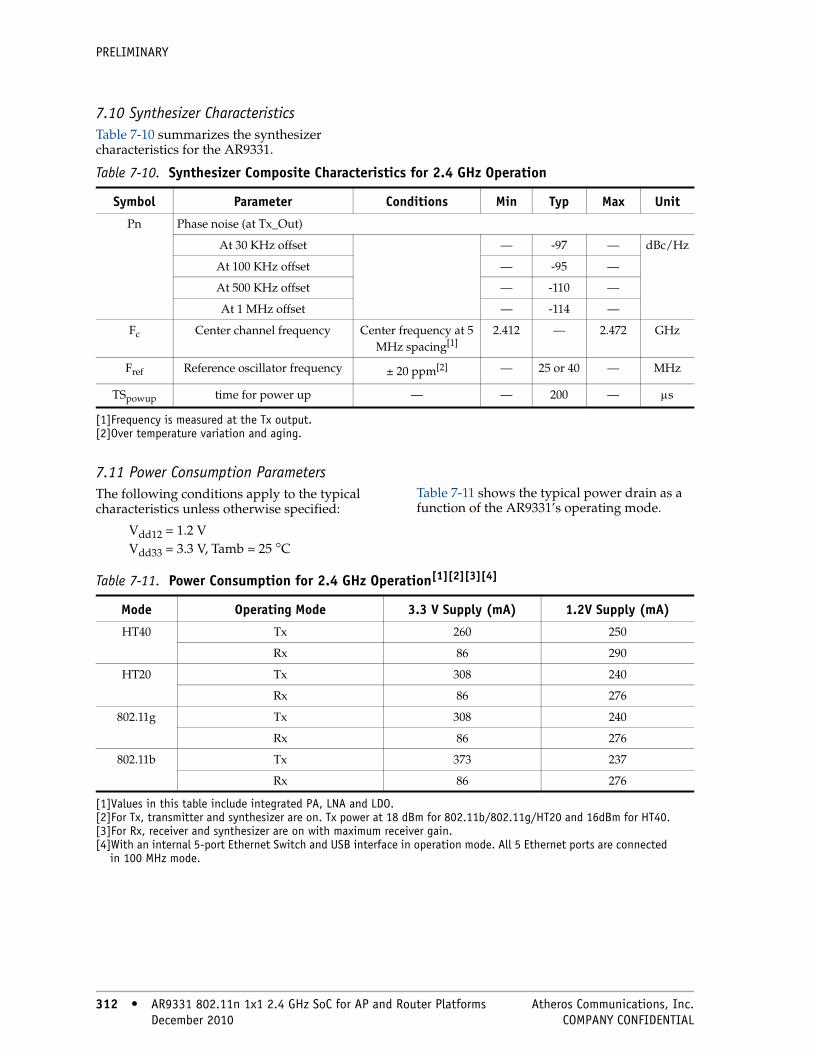
PRELIMINARY
7.10 Synthesizer Characteristics Table 7-10 summarizes the synthesizer characteristics for the AR9331.
7.11 Power Consumption ParametersThe following conditions apply to the typical characteristics unless otherwise specified:
Vdd12 = 1.2 V Vdd33 = 3.3 V, Tamb = 25 °C
Table 7-11 shows the typical power drain as a function of the AR9331’s operating mode.
Table 7-10. Synthesizer Composite Characteristics for 2.4 GHz Operation
Symbol Parameter Conditions Min Typ Max Unit
Pn Phase noise (at Tx_Out)
At 30 KHz offset — -97 — dBc/Hz
At 100 KHz offset — -95 —
At 500 KHz offset — -110 —
At 1 MHz offset — -114 —
Fc Center channel frequency Center frequency at 5 MHz spacing[1]
2.412 — 2.472 GHz
Fref Reference oscillator frequency ± 20 ppm[2] — 25 or 40 — MHz
TSpowup time for power up — — 200 — μs
[1]Frequency is measured at the Tx output.[2]Over temperature variation and aging.
Table 7-11. Power Consumption for 2.4 GHz Operation[1][2][3][4]
Mode Operating Mode 3.3 V Supply (mA) 1.2V Supply (mA)
HT40 Tx 260 250
Rx 86 290
HT20 Tx 308 240
Rx 86 276
802.11g Tx 308 240
Rx 86 276
802.11b Tx 373 237
Rx 86 276
[1]Values in this table include integrated PA, LNA and LDO.[2]For Tx, transmitter and synthesizer are on. Tx power at 18 dBm for 802.11b/802.11g/HT20 and 16dBm for HT40.[3]For Rx, receiver and synthesizer are on with maximum receiver gain.[4]With an internal 5-port Ethernet Switch and USB interface in operation mode. All 5 Ethernet ports are connected
in 100 MHz mode.
312 • AR9331 802.11n 1x1 2.4 GHz SoC for AP and Router Platforms Atheros Communications, Inc. 312 • December 2010 COMPANY CONFIDENTIAL

PRELIMINARY
8. Package DimensionsThe AR9331 is packaged in a dual-row LPCC package. The body size is 12 mm by 12 mm. The package drawings and dimensions are provided in Figure 8-1 and Figure 8-2, and Table 8-1.
Figure 8-1. AR9331 Package Drawing: Top View and Detail
TOP VIEW
FOR ODD OUTER TERMINAL/SIDE FOR EVEN OUTER TERMINAL/SIDE
SECTION "C-C"SCALE: NONE
Atheros Communications, Inc. AR9331 802.11n 1x1 2.4 GHz SoC for AP and Router Platforms • 313 COMPANY CONFIDENTIAL December 2010 • 313

PRELIMINARY
Figure 8-2. AR9331 Package Drawing: Bottom and Side View
SIDE VIEW
BOTTOM VIEW
314 • AR9331 802.11n 1x1 2.4 GHz SoC for AP and Router Platforms Atheros Communications, Inc. 314 • December 2010 COMPANY CONFIDENTIAL
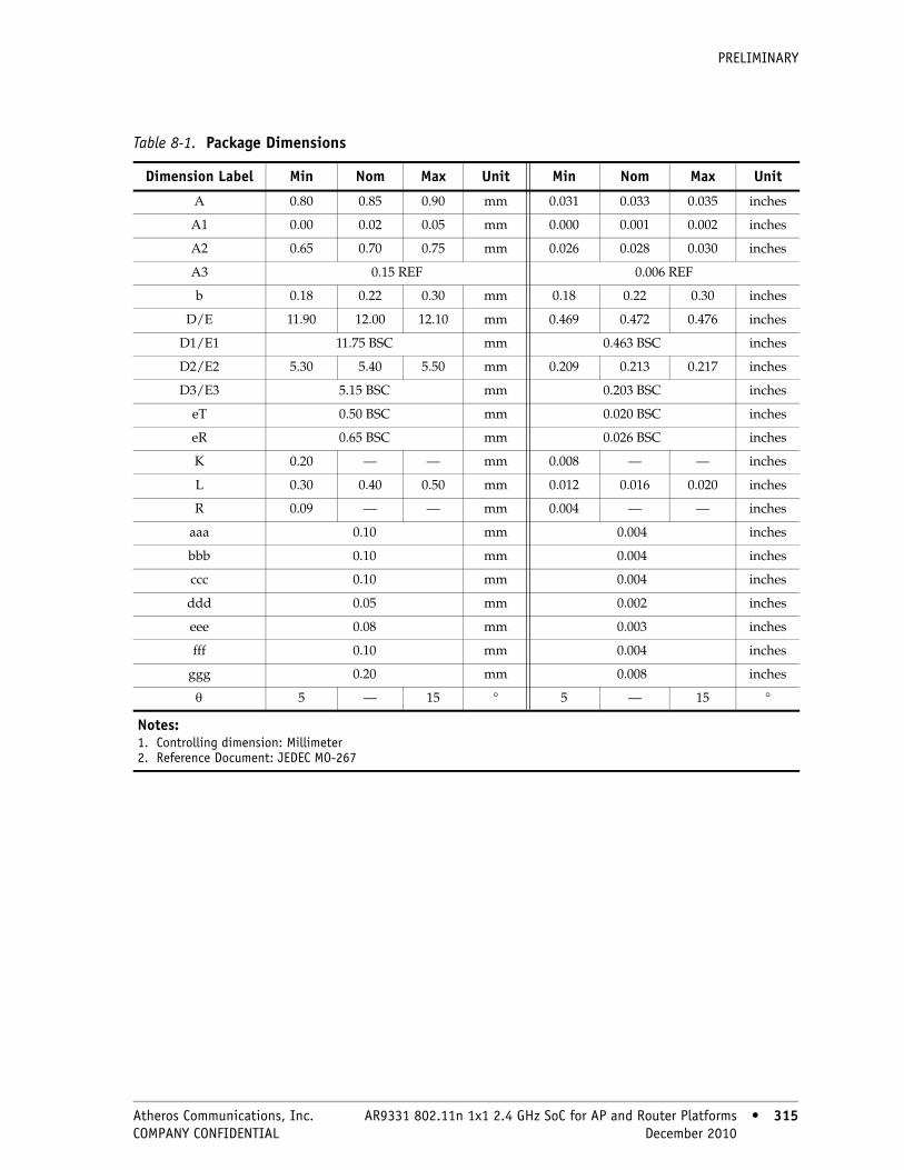
PRELIMINARY
Table 8-1. Package Dimensions
Dimension Label Min Nom Max Unit Min Nom Max Unit
A 0.80 0.85 0.90 mm 0.031 0.033 0.035 inches
A1 0.00 0.02 0.05 mm 0.000 0.001 0.002 inches
A2 0.65 0.70 0.75 mm 0.026 0.028 0.030 inches
A3 0.15 REF 0.006 REF
b 0.18 0.22 0.30 mm 0.18 0.22 0.30 inches
D/E 11.90 12.00 12.10 mm 0.469 0.472 0.476 inches
D1/E1 11.75 BSC mm 0.463 BSC inches
D2/E2 5.30 5.40 5.50 mm 0.209 0.213 0.217 inches
D3/E3 5.15 BSC mm 0.203 BSC inches
eT 0.50 BSC mm 0.020 BSC inches
eR 0.65 BSC mm 0.026 BSC inches
K 0.20 — — mm 0.008 — — inches
L 0.30 0.40 0.50 mm 0.012 0.016 0.020 inches
R 0.09 — — mm 0.004 — — inches
aaa 0.10 mm 0.004 inches
bbb 0.10 mm 0.004 inches
ccc 0.10 mm 0.004 inches
ddd 0.05 mm 0.002 inches
eee 0.08 mm 0.003 inches
fff 0.10 mm 0.004 inches
ggg 0.20 mm 0.008 inches
θ 5 — 15 ° 5 — 15 °
Notes:1. Controlling dimension: Millimeter2. Reference Document: JEDEC MO-267
Atheros Communications, Inc. AR9331 802.11n 1x1 2.4 GHz SoC for AP and Router Platforms • 315 COMPANY CONFIDENTIAL December 2010 • 315

PRELIMINARY
316 • AR9331 802.11n 1x1 2.4 GHz SoC for AP and Router Platforms Atheros Communications, Inc. 316 • December 2010 COMPANY CONFIDENTIAL
PRELIMINARY
9. Ordering InformationThe order number AR9331-AL1A specifies a lead-free standard-temperature version of the AR9331.
Atheros Communications, Inc. AR9331 802.11n 1x1 2.4 GHz SoC for AP and Router Platforms • 317 COMPANY CONFIDENTIAL December 2010 • 317

Atheros Communications, Incorporated5480 Great America Parkway
Santa Clara, CA 95054tel: 408.773.5200fax: 408.773.9940www.atheros.com
The information in this document has been carefully reviewed and is believed to be accurate. Nonetheless, this document is subject to change without notice. Atheros assumes no responsibility for any inaccuracies that may be contained in this document, and makes no commitment to update or to keep current the contained information, or to notify a person or organization of any updates. Atheros reserves the right to make changes, at any time, to improve reliability, function or design and to attempt to supply the best product possible.
Document Number: MKG-1517 Rev. 1
COMPANY CONFIDENTIALSubject to Change without Notice
Related Documents