Thank you for your continuing loyalty to Fujitsu's semiconductor products. Electronic equipment is continually becoming smaller, lighter, and less expensive while also growing more advanced in terms of function and performance. As a result, applications for semiconductor devices such as IC and LSI are rapidly increasing. Given this environment, package technology is rapidly increasing in importance. Fujitsu is working hard to develop packages that permit improved mounting efficiency. This data book demonstrates Fujitsu's technologies that are capable of responding to the growing diversification of packages, and includes all of Fujitsu's IC packages, from general-purpose packages to those that are still under development. This data book is intended for engineers who are using Fujitsu packages in the design of their products, and therefore focuses on the package outline drawings. Fujitsu Limited Electronic Devices Preface

Welcome message from author
This document is posted to help you gain knowledge. Please leave a comment to let me know what you think about it! Share it to your friends and learn new things together.
Transcript

Thank you for your continuing loyalty to Fujitsu's semiconductor products.
Electronic equipment is continually becoming smaller, lighter, and less
expensive while also growing more advanced in terms of function and
performance. As a result, applications for semiconductor devices such as IC and
LSI are rapidly increasing.
Given this environment, package technology is rapidly increasing in importance.
Fujitsu is working hard to develop packages that permit improved mounting
efficiency.
This data book demonstrates Fujitsu's technologies that are capable of
responding to the growing diversification of packages, and includes all of
Fujitsu's IC packages, from general-purpose packages to those that are still
under development.
This data book is intended for engineers who are using Fujitsu packages in the
design of their products, and therefore focuses on the package outline drawings.
Fujitsu LimitedElectronic Devices
Preface
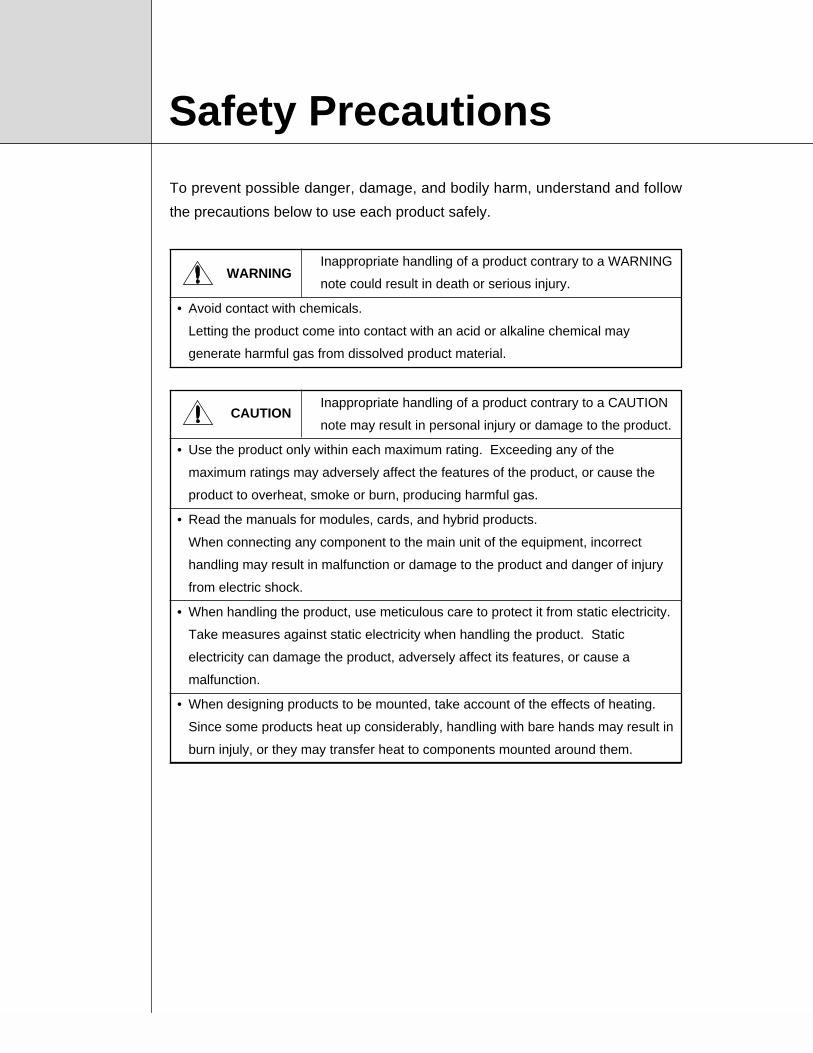
To prevent possible danger, damage, and bodily harm, understand and follow
the precautions below to use each product safely.
Inappropriate handling of a product contrary to a WARNING
note could result in death or serious injury.
• Avoid contact with chemicals.
Letting the product come into contact with an acid or alkaline chemical may
generate harmful gas from dissolved product material.
Inappropriate handling of a product contrary to a CAUTION
note may result in personal injury or damage to the product.
• Use the product only within each maximum rating. Exceeding any of the
maximum ratings may adversely affect the features of the product, or cause the
product to overheat, smoke or burn, producing harmful gas.
• Read the manuals for modules, cards, and hybrid products.
When connecting any component to the main unit of the equipment, incorrect
handling may result in malfunction or damage to the product and danger of injury
from electric shock.
• When handling the product, use meticulous care to protect it from static electricity.
Take measures against static electricity when handling the product. Static
electricity can damage the product, adversely affect its features, or cause a
malfunction.
• When designing products to be mounted, take account of the effects of heating.
Since some products heat up considerably, handling with bare hands may result in
burn injuly, or they may transfer heat to components mounted around them.
CAUTION
Safety Precautions
WARNING

Inappropriate handling of a product contrary to a CAUTION
note may result in personal injury or damage to the product.
•When mounting the product, satisfy the mounting conditions recommended by
Fujitsu.
Disregarding any of the mounting conditions may adversely affect the features of
the product or dissolve its material, producing harmful gas.
• When mounting a heat sink plate or fin on the product, be careful not to deform
the product.
If the part is mounted inappropriately, it may adversely affect the features of the
product.
• Be careful to avoid injury from pins.
Some products have sharp-ended pins for functional purpose.
• Be careful during ultrasonic cleaning.
Ultrasonic cleaning of ceramic packages or ceramic modules may adversely affect
them, for example, by vibrating internal wires, resulting in breaks. For plastic
packages, observe the cleaning conditions recommended by Fujitsu.
• When mounting modules, cards, or hybrid products, use a non-deforming method
at an appropriate temperature.
Incorrect mounting may result in defective products.
• Do not use the product where corrosive gas is generated.
Corrosive gas may adversely affect the features of the product, for example, by
degrading its characteristics by corrosion.
• When discarding the product, refer to an authorized disposal or recycling
company.
Burning the product for disposal may generate harmful gas.
CAUTION
Precautionary Information for Handling of Semiconductor Devices
Any semiconductor devices have inherently a certain rate of failure. The possibility of failure is greatly affected by
the conditions in which they are used (circuit conditions, environmental conditions, etc.). This page describes
precautions that must be observed to minimize the chance of failure and to obtain higher reliability from your
FUJITSU semiconductor devices.
1. Precautions for Product Design
This section describes precautions when designing electronic equipment using semiconductor devices.
1.1 Absolute Maximum Ratings
Semiconductor devices can be permanently damaged by application of stress (voltage, current, temperature,
etc.) in excess of certain established limits, called absolute maximum ratings. Do not exceed these ratings.
1.2 Recommended Operating Conditions
Recommended operating conditions are normal operating ranges for the semiconductor device. All the
device's electrical characteristics are warranted when operated within these ranges.
Always use semiconductor devices within the recommended operating conditions. Operation outside these
ranges may adversely affect reliability and could result in device failure.
No warranty is made with respect to uses , operating conditions, or combinations not represented on the data
sheet. Users considering application outside the listed conditions are advised to contact their FUJITSU sales
representative beforehand.
1.3 Processing and Protection of Pins
These precautions must be followed when handling the pins which connect semiconductor devices to power
supply and input/output functions.
(a) Preventing Over-Voltage and Over-Current Conditions
Exposure to voltage or current levels in excess of maximum ratings at any pin is likely to cause deteriora-
tion within the device, and in extreme cases leads to permanent damage of the device. Try to prevent such
over-voltage or over-current conditions at the design stage.
(b) Protection of Output Pins
Shorting of output pins to supply pins or other output pins, or connection to large capacitance can cause
large current flows. Such conditions if present for extended periods of time can damage the device.
Therefore, avoid this type of connection.
(c) Handling of Unused Input Pins
Unconnected input pins with very high impedance levels can adversely affect stability of operation. Such
pins should be connected through an appropriate resistance to a power supply pin or ground pin.

Precautionary Information for Handling of Semiconductor Devices
1.4 Latch-up
Semiconductor devices are constructed by the formation of P-type and N-type areas on a substrate. When
subjected to abnormally high voltages, internal parasitic PNPN junctions (called thyristor structures) may be
formed, causing large current levels in excess of several hundred mA to flow continuously at the power supply
pin. This condition is called latch-up.
CAUTION: The occurrence of latch-up not only causes loss of reliability in the semiconductor device, but can
cause injury or damage from high heat, smoke or flame. To prevent this from happening, do the following:
(a) Be sure that voltages applied to pins do not exceed the absolute maximum ratings. This should include
attention to abnormal noise, surge levels, etc.
(b) Be sure that abnormal current flows do not occur during the power-on sequence.
1.5 Observance of Safety Regulations and Standards
Most countries in the world have established standards and regulations regarding safety, protection from
electromagnetic interference, etc. Customers are requested to observe applicable regulations and standards
in the design of products.
1.6 Fail-Safe Design
Any semiconductor devices have inherently a certain rate of failure. You must protect against injury, damage
or loss from such failures by incorporating safety design measures into your facility and equipment such as
redundancy, fire protection, and prevention of over-current levels and other abnormal operating conditions.
1.7 Precautions Related to Usage of Devices
FUJITSU semiconductor devices are intended for use in standard applications (computers, office automation
and other office equipment, industrial, communications, and measurement equipment, personal or household
devices, etc.).
CAUTION: Customers considering the use of our products in special applications where failure or abnormal
operation may directly affect human lives or cause physical injury or property damage, or where extremely
high levels of reliability are demanded (such as aerospace systems, atomic energy controls, sea floor repeat-
ers, vehicle operating controls, medical devices for life support, etc.) are requested to consult with FUJITSU
sales representatives before such use. The company will not be responsible for damages arising from such
use without prior approval.
2. Precautions for Package Mounting
Package mounting may be either lead insertion type or surface mount type. In either case, for heat resistance
during soldering, you should only mount under FUJITSU's recommended conditions. For detailed information
about mount conditions, contact your FUJITSU sales representative.

Precautionary Information for Handling of Semiconductor Devices
2.1 Lead Insertion Type
Mounting of lead insertion type packages onto printed circuit boards may be done by two methods: direct
soldering on the board, or mounting by using a socket.
Direct mounting onto boards normally involves processes for inserting leads into through-holes on the board
and using the flow soldering (wave soldering) method of applying liquid solder. In this case, the soldering
process usually causes leads to be subjected to thermal stress in excess of the absolute ratings for storage
temperature. Mounting processes should conform to FUJITSU recommended mounting conditions.
If socket mounting is used, differences in surface treatment of the socket contacts and IC lead surfaces can
lead to contact deterioration after long periods. For this reason it is recommended that the surface treatment
of socket contacts and IC leads be verified before mounting.
2.2 Surface Mount Type
Surface mount packaging has longer and thinner leads than lead-insertion packaging, and therefore leads are
more easily deformed or bent. The use of packages with higher pin counts and narrower pin pitch results in
increased susceptibility to open connections caused by deformed pins, or shorting due to solder bridges.
You must use appropriate mounting techniques. FUJITSU recommends the solder reflow method, and has
established a ranking of mounting conditions for each product. Users are advised to mount packages in
accordance with FUJITSU ranking of recommended conditions.
2.3 Storage of Semiconductor Devices
Because plastic chip packages are formed from plastic resins, exposure to natural environmental conditions
will cause absorption of moisture. During mounting, the application of heat to a package that has absorbed
moisture can cause surfaces to peel, reducing moisture resistance and causing packages to crack. To pre-
vent, do the following:
(a) Avoid exposure to rapid temperature changes, which cause moisture to condense inside the product.
Store products in locations where temperature changes are slight.
(b) Use dry boxes for product storage. Products should be stored below 70% relative humidity, and at tem-
peratures between 5 °C (41 °F) and 30 °C (86 °F).
(c) When necessary, FUJITSU packages semiconductor devices in highly moisture-resistant aluminum lami-
nate bags, with a silica gel desiccant. Devices should be sealed in their aluminum laminate bags for
storage.
(d) Avoid storing packages where they are exposed to corrosive gases or high levels of dust.
2.4 Baking
Packages that have absorbed moisture may be de-moisturized by baking (heat drying). Follow the FUJITSU
recommended conditions for baking.

Precautionary Information for Handling of Semiconductor Devices
2.5 Static Electricity
Because semiconductor devices are particularly susceptible to damage by static electricity, you must take the
following precautions:
(a) Maintain relative humidity in the working environment between 40% and 70%. Use of an apparatus for ion
generation may be needed to remove electricity.
(b) Electrically ground all conveyors, solder vessels, soldering irons and peripheral equipment.
(c) Eliminate static body electricity by the use of rings or bracelets connected to ground through high resis-
tance (on the level of 1MW).
Wearing of conductive clothing and shoes, use of conductive floor mats and other measures to minimize
shock loads is recommended.
(d) Ground all fixtures and instruments, or protect with anti-static measures.
(e) Avoid the use of styrofoam or other highly static-prone materials for storage of completed board assem-
blies.
3. Precautions for Use Environment
Reliability of semiconductor devices depends on ambient temperature and other conditions as described
above. For reliable performance, do the following:
(a) Humidity
Prolonged use in high humidity can lead to leakage in devices as well as printed circuit boards. If high
humidity levels are anticipated, consider anti-humidity processing.
(b) Discharge of Static Electricity
When high-voltage charges exist close to semiconductor devices, discharges can cause abnormal opera-
tion. In such cases, use anti-static measures or processing to prevent discharges.
(c) Corrosive Gases, Dust, or Oil
Exposure to corrosive gases or contact with dust or oil may lead to chemical reactions that will adversely
affect the device. If you use devices in such conditions, consider ways to prevent such exposure or to
protect the devices.
(d) Radiation, Including Cosmic Radiation
Most devices are not designed for environments involving exposure to radiation or cosmic radiation. Users
should provide shielding as appropriate.
(e) Smoke, Flame
CAUTION: Plastic molded devices are flammable, and therefore should not be used near combustible sub-
stances. If devices begin to smoke or burn, there is danger of the release of toxic gases.
Customers considering the use of FUJITSU products in other special environmental conditions should consult
with FUJITSU sales representatives.

This data book consists of six chapters.
Chapter 1: Introduction to Packages
This chapter provides an overview of packages, and describes their
organization, forms, and structure, and also discusses future trends in
packages.
Chapter 2: Package Mounting Methods
This chapter explains mounting methods, humidity resistance characteristics,
and handling, focusing especially on surface mounting packages since they
require particular care in terms of mounting techniques.
Chapter 3: Package Lineup
This chapter shows the correspondence between package form and the number
of pins, and lists the package lineup.
Chapter 4: Package Outline Diagrams
This chapter first describes how the package dimensions are displayed and also
explains the package codes. The remainder of the chapter is devoted to the
package outline diagrams, showing one package per page.
Chapter 5: Sockets
This chapter explains sockets.
Chapter 6: Packaging for Shipment
This chapter explains packaging for shipment.
Organization of ThisData Book

When you want to find a particular piece of information within a given section,
there are the following additional means for locating that information, aside from
the normal table of contents and index:
• Searching for information in the package lineup
The package lineup is displayed in charts grouped according to the package
form and material. The package codes are listed in the chart in sequence,
starting from the least number of pins. (Refer to section 2 of chapter 3.)
• Searching for information from the package form and number of pins
The thumb indices and headers are convenient. Each page in the package
outline diagram section has a thumb index and a header. The thumb index
indicates the package form, while the header indicates the form and the number
of pins.
How to Use This Document

85
DIP
PLA
ST
IC
DUAL IN-LINE PACKAGE8 PIN PLASTIC
8-pin plastic DIP Lead pitch
Row spacing
Sealing method
100mil
300mil
Plastic mold
DIP-8P-M01EIAJ code:*DIP008-P-0300-1
(DIP-8P-M01)
8-pin plastic DIP(DIP-8P-M01)
Dimensions in mm (inches).
+0.30
–0+.012 +.012
–0
+.016–.012
–.012+.014
–0+0.30
–0
+0.40–0.30
–0.30+0.35
(.244±.010)6.20±0.251 PIN INDEX
15°MAX
TYP7.62(.300)
0.51(.020)MIN
(.010±.002)0.25±0.05
(.018±.003)0.46±0.08
TYP2.54(.100)
3.00(.118)MIN
4.36(.172)MAX
.039 .060
.370
.035
1.520.99
9.40
0.89
1994 FUJITSU LIMITED D08006S-2C-3C
Package Outline Diagram PageLayout Used in This Data Book
Packagecode
Header: Shows form and number of pins
Tab: Shows form
Package outlinediagram
Illustration
Characteristics

3
Overview
1.1 Overview
Fujitsu provides semiconductor packages as a kind of "interposers" for protecting semiconduc-tor devices and getting the full benefit of them. Fujitsu has developed and released a diversi-fied series of "general-purpose package families" supporting a wide range of applications tosuit customers' needs. The packages include through-hole type packages such as DIPs andPGAs; QFPs and SOPs that contributed to setting the trend of surface mounting; and multi-pinQFPs, TCPs, and SVPs supporting high-tensity mounting.
In addition, Fujitsu has developed and provided custom packages, cards, and modules forspecific customers.
This chapter begins with Fujitsu's package lineup, followed by descriptions of package shapesand structures.
This chapter also describes the package dimension display conventions and package codebased on the EIAJ and JEDEC*1 standards to help you use this data book more efficiently as asource of information for you.
Also, this chapter introduces Fujitsu's basic concept of package development for futurepackages.
The electronic device marketplace has been demanding more advanced and diversified high-density mounting technologies.
Fujitsu has developed new packages such as SONs and FBGAs to meet the needs of theindustry. To support customers for easier use of these new packages, at the same time, Fujitsuhas made a strong commitment to standardization of the packages by EIAJ*2.
*1: Joint Electron Device Engineering Council
*2: Electronic Industries Association of Japan

4
Package Lineup
1.2 Package LineupThe packages are classified as follows, according to form, material, and the mounting methodsfor which they are suited.
Packages Lead inserted type DIPStandardHorizontal type,Double lead
WDIPWindow type
SDIPSmall outline
PGAMatrix type Standard
SVPSurface mounted type Vertical type,Single lead
SOPDual leadFlat type
TSOP I
TSOP II
LSSOP
TSSOP
QFPQuad lead
LQFP
TQFP
UQFP
HQFP
TPQFP
SONLeadless chip carrier Dual lead
SOJJ-lead type Dual lead
QFJQuad lead
BGAMatrix type
SPGA
LGA
DTPDual leadTape carrier
Quad lead QTP
SIMM
DIMM
DIP
QFP
Socket type
Modules Socket type
Piggyback type
Cards
QFNQuad lead

5
*1: These columns indicate the dimensions shown at right.
*2: Joint Electron Device Engineering Council
*3: Package name used by Fujitsu
Row space
Lead pitch
100 mil = 2.54 mm
egakcapfoemaN noitpircseD *hctipdaeL 1 )mm( *ecapswoR 1 )mm(
PID egakcaPenil-nIlauD 45.2 68.22/42.51/61.01/26.7
*PID-HS 3 egakcaPenil-nIlauDknirhS 877.1 –
*PID-KS 3 egakcaPenil-nIlauDynnikS 45.2 26.7
*PID-LS 3 egakcaPenil-nIlauDmilS 45.2 61.01
PIZS egakcaPenil-nIgaZ-giZknirhS 98.0 877.1
AGP egakcaPyarrAdirGniP 45.2/72.1 –
PVS egakcaPlacitreVecafruS 56.0/5.0 –
POS)daelthgiarts(egakcaPeniltuOllamS
egakcaPdedaeL-LeniltuOllamS72.1 –
*LOS 3 *CEDEJ(egakcaPdedaeL-LeniltuOllamS 2) 72.1 –
POSS egakcaPdedaeL-LeniltuOllamSknirhS 00.1/08.0/56.0 –
)I(POST )I(egakcaPdedaeL-LeniltuOllamSnihT 06.0/55.0/05.0 –
)II(POST )II(egakcaPdedaeL-LeniltuOllamSnihT/08.0/05.0
72.1/00.1–
NOS egakcaPdedaeL-noNeniltuOllamS 00.1/05.0 –
PFQ)daelthgiarts(egakcaPtalFdauQ
egakcaPdedaeL-LtalFdauQ
/05.0/04.0/08.0/56.0
00.1–
*PFQL 3 egakcaPdedaeL-LtalFdauQeliforpwoL/05.0/04.0
08.0/56.0–
PFQT egakcaPdedaeL-LtalFdauQnihT 05.0/04.0 –
PFQH kniStaeHhtiwPFQ/05.0/04.0
56.0–
PFQPT daPtseThtiwPFQ 03.0 –
*CCL 3 reirraCpihCsseldaeL72.1/610.1 –
NFQ )JAIE(egakcaPdedaeL-noNtalFdauQ
*PLCP 3 egakcaPsseldaeLdraob-tiucriCdetnirP 56.0/05.0 –
JFQ )JAIE(egakcaPdedaeL-JtalFdauQ 72.1 –
JOS egakcaPdedaeL-JeniltuOllamS 72.1 –
AGB yarrAdirGllaB 0.1/72.1/5.1 –
PTD egakcaPreirraCepaTlauD – –
PTQ egakcaPreirraCepaTdauQ – –
MMIS eludoMyromeMenilnIelgniS 45.2/72.1 –
MMID eludoMyromeMenilnIlauD 72.1 –
Package Lineup

6
Lead pitch
Standard : 100 mil
Standard: 70 mil
Standard : 100 mil
Standard : 100 mil
0.50mm0.65mm
Standard: 50 mil
Features
The leads on this package extend down fromthe sides of the package in two rows. This iscurrently the most typical standard package.
The row spacing varies according to thenumber of pins, as follows:8 to 20 pins: 300 mil 24 to 52 pins: 600 mil
22 to 28 pins: 400 mil 64 pins or more: 900 mil
This is a standard DIP with the lead pitchreduced from 100 mil to 70 mil (1.778 mm). In
some versions, both the lead pitch and the rowspacing are reduced. The benefit of thereduced pitch is greatest when there are a
large number of leads.
This is a standard DIP with the row spacingreduced to 300 mil in the case of the "SK-DIP"
and 400 mil in the case of the "SL-DIP."SK-DIP: 300 mil, 22/22/28/32 pinsSK-DIP: 400 mil, 24/28 pins
The leads on this package extend straight
down from the bottom of the package in a gridarrangement. This package is suited for high-density mounting of packages with 64 or more
pins. A special version with a lead pitch of 50mil is available.
This type of package is placed perpendicular to
the printed circuit board and can then besurface mounted.
The leads on these packages extend out from
two edges of the package; the leads are eithergullwing (L-shaped) or straight.Packages that conform with JEDEC
specifications are called "SOL".
Name ofpackage
DIP
SH-DIP*
SK-DIP*
SL-DIP*
PGA
SVP
SOPSOL*
Package Forms
1.3 Package FormsPackages can be broadly classified into two types according to the mounting method used:
Lead inserted type: The leads on the package are inserted into through holes in aprinted circuit board, etc., and then soldered in place.
Surface mounted type: The device lays flat on surface of the circuit board and theleads are soldered directly to the wires.
In addition, each of the various package forms has its own unique features.
1.3.1 Lead insertion types
Illustration
*: Package name used by Fujitsu.

7
Lead pitch
1.00mm0.80mm
0.65mm
SSOP:0.65mm/0.80mm/1.00mm
LQFP:0.40mm/0.50mm
TSOP: 0.50mm/
0.55mm/0.60mmTQFP: 0.40mm/0.50mm
0.5mm/1.0mm
0.30mm
Standard: 50 milAmong LCCs with manypads, 40-mil, 25-mil andother fine-pitch packagesare currently underdevelopment.
0.50mm
0.65mm
Name ofpackage
QFP
SSOPLQFP*
TSOP
TQFP
SON
TPQFP
LCCQFN
PCLP
Features
The leads on this package extend out from foursides of the package; the leads are eithergullwing (L-shaped) or straight.
These packages are compact versions of theSOP and QFP. (The lead pitch and body sizeare smaller.)
These packages are thinner versions of theSOP and QFP. (Mounted height: 1.27 mm
max.)
This type of package has external electrodesprovided in two directions on the surface of thepackage. The package is a smaller version of
the TSOP. It can be handled easily because ofno bent leads.
This is a fine-pitch QFP package with fixed testpads located around the periphery of the
package and body. Excellent lead precision ispossible by mounting a holder.
This package has no leads; instead, it has onlyelectrode pads for soldering. A ceramicleadless chip carrier is a compact, high-
reliability representative of this type ofpackage.
This package has no leads; instead, it has onlyelectrode pads for soldering. A plastic leadless
chip carrier is a compact representative of thistype of package.
Package Forms
1.3.2 Surface mounted types
Illustration
(continued)*: Package name used by Fujitsu.

8
Lead pitch
Standard: 50 mil
0.50 to 0.15mm
Name ofpackage
QFJ
SOJ
DTP
QTP
Features
The leads on this type of package are bentdown from the sides of the package in a Jshape. Of these packages, those with leads onQuad are called QFJ packages, while thosewith leads on dual are called SOJ packages.
This type of package, generally called a "TABpackage," consists of an IC chip mounted bymeans of TAB technology on a tape on whichthe wiring pattern is formed; the chip is thencoated with resin. This package is suited forthe increasing number of pins required in chipsand for high-density mounting. There are threetape widths: 35 mm, 48 mm, and 70 mm.
Package Forms
(continued)
Illustration
JAPAN
160-0
1
1.3.3 SMD module, piggyback, card
Name ofpackage
SMDmodule
Piggyback
Card
Features
This module consists of multiple small surface mounted packages (SMDs)
on a ceramic or resin motherboard. These modules are primarily used formemory and permit higher densities and more advanced systems. Thepins are arranged in either a SIP, DIP or ZIP pattern. The module is alsoavailable in a socket form that permits easy insertion and removal for future
memory expansion.
This package consists of a ceramic package with a socket mounted on it,
and can be used to plug in LCC, DIP and other types of packages. Thepins are arranged in either DIP form or QFP form. This type of package isused for program evaluation and system operation testing in the
development of microcomputer-based systems.
This type of package consists of multiple elements or chip-type passiveelements mounted on a resin wiring substrate. Cards are used for PC
cards, DRAM cards, miniature cards, etc.
Illustration

9
Au plating or
Sn plating
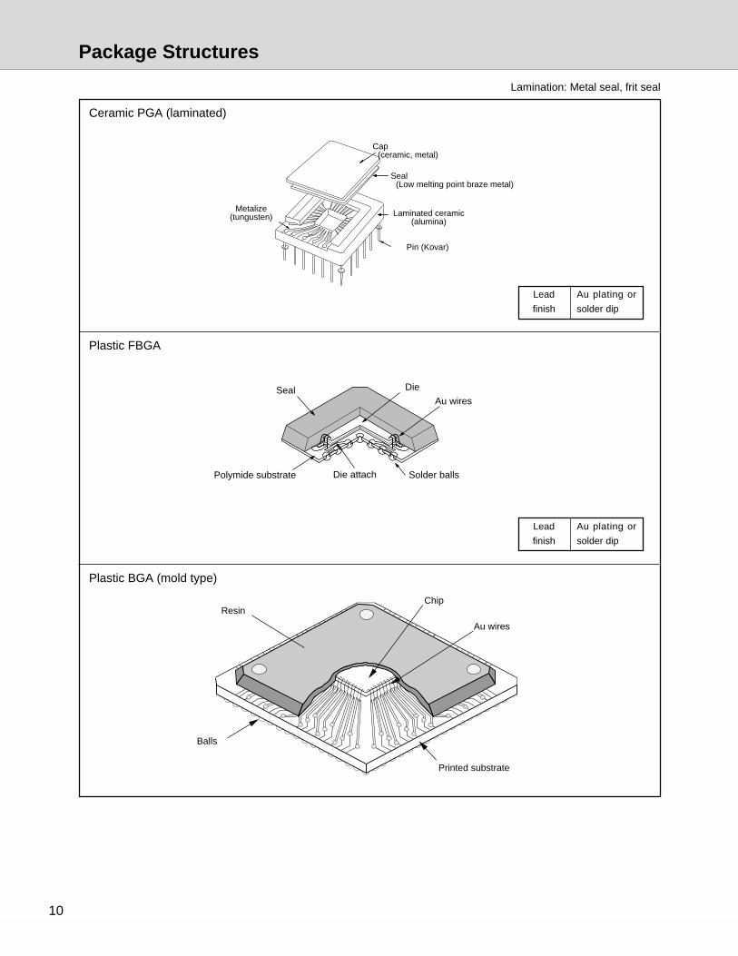
Package Structures
1.4 Package Structures
1.4.1 Structure diagrams
Structure diagrams for typical packages are shown below.
Lamination: Metal seal, frit seal
Plastic DIP
Ceramic DIP (laminated)
Ceramic DIP (cerdip)
Lead
finish
Lead
finish
Solder
plating
Sn platingLead
finish
Lead frame(Fe-Ni alloy)
Low melting point glass
Ceramic cap(alumina)
Ceramic base(alumina)
(
Resin
Au wires
Chip
Lead frameFe-Ni alloy
orCu alloy )
Lead frameKovar
orFe-Ni alloy)
Cap(metal, ceramic)
Seal(low melting point braze metal,low melting point glass)
Metalize(tungusten)
Laminated firing ceramic(alumina) (
10
Package Structures
Lamination: Metal seal, frit seal
Ceramic PGA (laminated)
Plastic FBGA
Plastic BGA (mold type)
Au plating or
solder dip
Lead
finish
Au plating or
solder dip
Lead
finish
Cap(ceramic, metal)
Seal(Low melting point braze metal)
Metalize(tungusten) Laminated ceramic
(alumina)
Pin (Kovar)
Au wiresSeal
Die attachPolymide substrate Solder balls
Die
Printed substrate
Au wires
Balls
ChipResin

11
Package Structures
Lamination: Metal seal, frit seal
Plastic BGA (cavity down type)
Plastic SON
Plastic BCC
Solder platingLead
finish
Pd/Ni/Pd platingLead
finish
Resin
Chip
Multilayer printed substrate
Au wires
Solder balls
Stage
Inner lead
Resin
Chip
Pin
AU wires
Pin
AU bumpAU wiresLSI
Resin

12
Package Structures
Lamination: Metal seal, frit seal
Plastic QFP
SMD hybrid IC
Plastic QFJ
Solder platingLead
finish
Solder platingLead
finish
Solder platingLead
finish
(
Resin
Au wiring
Chip
Lead frameFe-Ni alloy
orCu alloy )
Resistor(thick film)
Lead frame (Cu alloy)
Chip
Au wiring
Substrate(ceramic)
Capacitor(Ceramic chip)
Resin
ResinChip
Au wiring
Lead frame (Cu alloy)

13
Lamination: Metal seal, frit seal
Tape carrier package
Sn platingLead
finish
Chip
Inner lead (Cu)
Test pad
Outer lead(Cu)
Resin
Package Structures
14
Package Structures
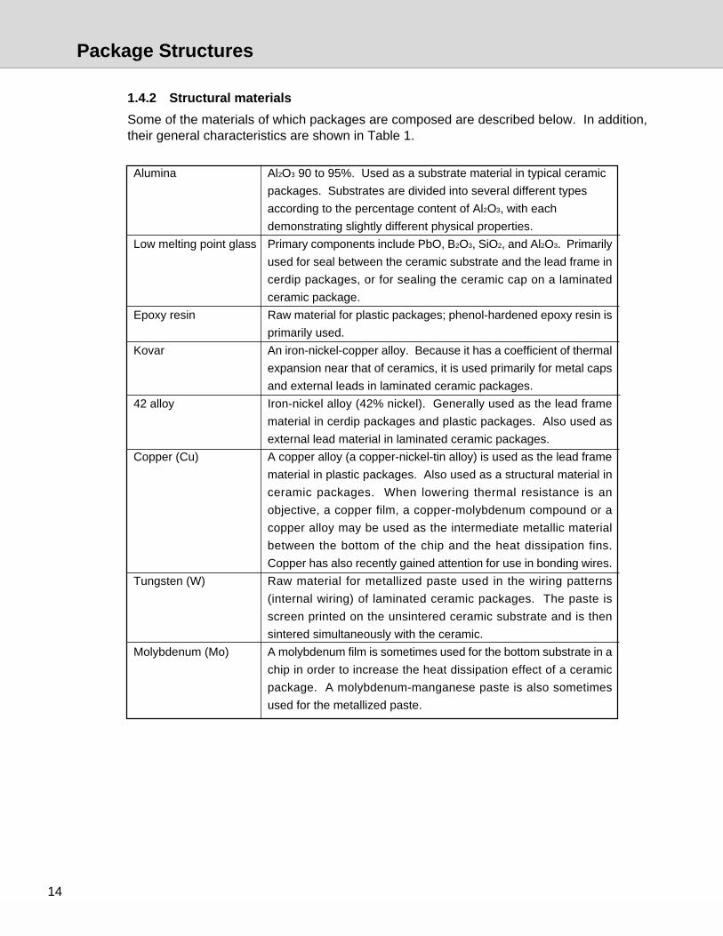
1.4.2 Structural materials
Some of the materials of which packages are composed are described below. In addition,their general characteristics are shown in Table 1.
Alumina
Low melting point glass
Epoxy resin
Kovar
42 alloy
Copper (Cu)
Tungsten (W)
Molybdenum (Mo)
Al2O3 90 to 95%. Used as a substrate material in typical ceramic
packages. Substrates are divided into several different types
according to the percentage content of Al2O3, with each
demonstrating slightly different physical properties.
Primary components include PbO, B2O3, SiO2, and Al2O3. Primarily
used for seal between the ceramic substrate and the lead frame in
cerdip packages, or for sealing the ceramic cap on a laminated
ceramic package.
Raw material for plastic packages; phenol-hardened epoxy resin is
primarily used.
An iron-nickel-copper alloy. Because it has a coefficient of thermal
expansion near that of ceramics, it is used primarily for metal caps
and external leads in laminated ceramic packages.
Iron-nickel alloy (42% nickel). Generally used as the lead frame
material in cerdip packages and plastic packages. Also used as
external lead material in laminated ceramic packages.
A copper alloy (a copper-nickel-tin alloy) is used as the lead frame
material in plastic packages. Also used as a structural material in
ceramic packages. When lowering thermal resistance is an
objective, a copper film, a copper-molybdenum compound or a
copper alloy may be used as the intermediate metallic material
between the bottom of the chip and the heat dissipation fins.
Copper has also recently gained attention for use in bonding wires.
Raw material for metallized paste used in the wiring patterns
(internal wiring) of laminated ceramic packages. The paste is
screen printed on the unsintered ceramic substrate and is then
sintered simultaneously with the ceramic.
A molybdenum film is sometimes used for the bottom substrate in a
chip in order to increase the heat dissipation effect of a ceramic
package. A molybdenum-manganese paste is also sometimes
used for the metallized paste.
15
Package Structures
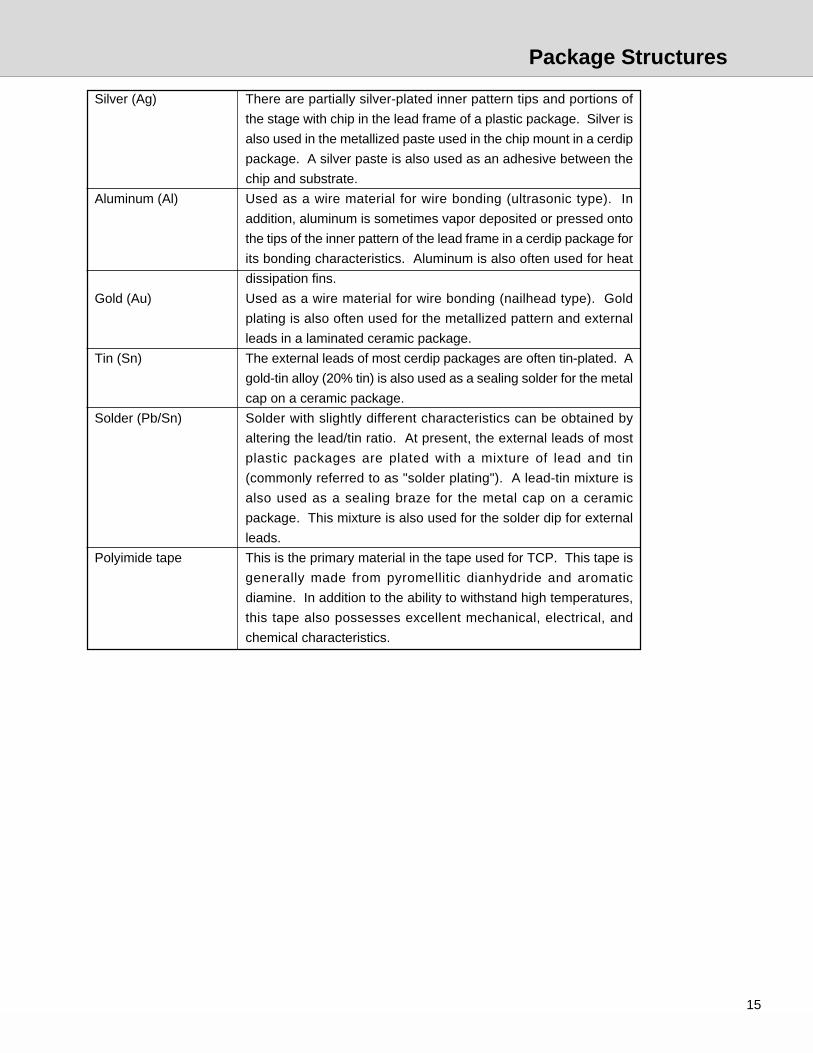
Silver (Ag)
Aluminum (Al)
Gold (Au)
Tin (Sn)
Solder (Pb/Sn)
Polyimide tape
There are partially silver-plated inner pattern tips and portions of
the stage with chip in the lead frame of a plastic package. Silver is
also used in the metallized paste used in the chip mount in a cerdip
package. A silver paste is also used as an adhesive between the
chip and substrate.
Used as a wire material for wire bonding (ultrasonic type). In
addition, aluminum is sometimes vapor deposited or pressed onto
the tips of the inner pattern of the lead frame in a cerdip package for
its bonding characteristics. Aluminum is also often used for heat
dissipation fins.
Used as a wire material for wire bonding (nailhead type). Gold
plating is also often used for the metallized pattern and external
leads in a laminated ceramic package.
The external leads of most cerdip packages are often tin-plated. A
gold-tin alloy (20% tin) is also used as a sealing solder for the metal
cap on a ceramic package.
Solder with slightly different characteristics can be obtained by
altering the lead/tin ratio. At present, the external leads of most
plastic packages are plated with a mixture of lead and tin
(commonly referred to as "solder plating"). A lead-tin mixture is
also used as a sealing braze for the metal cap on a ceramic
package. This mixture is also used for the solder dip for external
leads.
This is the primary material in the tape used for TCP. This tape is
generally made from pyromellitic dianhydride and aromatic
diamine. In addition to the ability to withstand high temperatures,
this tape also possesses excellent mechanical, electrical, and
chemical characteristics.

16
Packag
e Stru
ctures
Table 1. General Characteristics of Package Materials
Alumina (Al2O3
90% to 95%)
3.6 to 3.9
to 6.5 to 7.0
0.04
to 0.20
1012 to 1014
8.7 to 9.6
6.5 to 8.9
to 1100 to 1300
26 to 30
—
to 2100 to 2800
Lowmelting
point glass(LS-0110)
4.8
to 5.3
0.0032
—
to 109
to 12
to 19
—
6.87
—
to 450
Kovar
8.4
(5.1 to5.5)
0.04
0.11
49x10–6
—
—
to160
to14
(5000 to9000)
—
42alloy
8.2
(6.7 to7.4)
0.03
—
58x10–6
—
—
170 to240>
(15 to16)
—
—
Tungsten(W)
19.1
to 4.5
0.423
0.033
5.5x10⁻⁶
—
—
250 to490
to 37
(1300 to47000)
to 5200
Al
2.69
(23 to29)
0.569
0.21
2.75x10⁻⁶
—
—
—
7.17
to1020
—
Molybde-num (Mo)
10.2
(3.7 to5.3)
0.342
0.072
5.6x10⁻⁶
—
—
—
to 35
—
—
Au
19.3
to 14
0.762
0.030
2.4x10⁻⁶
—
—
—
to 7.95
(2040 to2550)
—
Ag
10.5
to 19
1.022
0.056
1.62x10⁻⁶
—
—
—
to 8.1
—
—
Cu
8.93
to 16.7
0.963
to 0.091
1.72x10⁻⁶
—
—
to 80
to 12.5
to 2500
—
Epoxyresin
to 1.8
to 18
to 1.4x10⁻³>
—
1015≥
to 4.3
—
—
1.4<
—
to 1000>
Pb/Sn(eutectic)
8.45
24.5
0.122
to 0.042
17x10–6
—
—
—
to 3.2
to 560
—
Sn
7.3
to 22
0.16
0.05
11.5x10⁻⁶
—
—
—
4.99
—
—
Material
Characteristic
Specific gravity
Coefficient of thermal expansion(x10–6/C) (40~400)
Thermal propagation(cal • cm/cm2 • sec • C°)
Specific heat(cal/g • C°)
Volume resistivity(Ω • cm) (20C°)
Permittivity (1 MHz)
Dielectric loss(x10–4)
Vickers hardness
Young's modulus(x105kg/cm2)
Tensile strength(kg/cm2)
Bending strength(kg/cm2)

17
1.5 How Package Dimensions Are Indicated
This section will use representative DIP and FLAT (SOP) packages to explain the manner inwhich dimensions are indicated in the package outline dimension diagrams in this data book.
1.5.1 DIP dimensions (in accordance with EIAJ IC-74-3)
How Package Dimensions Are Indicated
Dimension name
Mounting height
Standoff height
Height of body
Pin width
Maximum pin width
Pin thickness
Package length
Package width
Pin linear spacing
Pin linear spacing
Pin length
Pin angle
Overhang
Explanation
Height from the mounting surface to the top of the package
Distance between the mounting surface and the bottom of the package
Height (thickness) of the package body
Width of the portion of the pin inserted into the mounting hole in the
printed circuit board, etc.
Maximum width of the pin
Thickness of the pin
The longest dimension of the body of the package parallel to the
mounting surface and excluding the pins; also include resin burrs
The width of the body of the package, excluding the pins
Linear spacing between the centers of the pins; also called the "lead pitch"
Width between the rows of the pins; also called the "row spacing"
Length from the mounting surface to the tip of the pin
Angle of spread between the pin and a line perpendicular to the
mounting surface
Distance from the center position of an end pin to the end of the body
of the package
Symbol
A
A1
A2
b1
b, B1
C
D
E
e
e1
L
θ
Z
D
n n-1
21
E
A
L
A2B1
Z e e e e Z
bA1
X
Mountingplane
b1
e1
C
21 3Details *
*
θ θ
M

18
Symbol
A
A1
A2
b
c
D
E
e
e1
HE
L
θ
Z
How Package Dimensions Are Indicated
1.5.2 FLAT (SOP) dimensions (in conformity with EIAJ IC-74-2)
Dimension name
Mounting height
Standoff height
Height of body
Pin width
Pin thickness
Package length
Package width
Pin linear spacing
Call dimension
Overall width
Length of flat
portion of pin
Angle of flat portion
of pin
Overhang
Pin center tolerance
Uniformity of pin
bottoms
Explanation
Height from the mounting surface to the top of the package
Distance between the mounting surface and the bottom of the package
Thickness of the package (height of the body)
Width of the pin
Thickness of the pin
The longest dimension of the body of the package parallel to the
mounting surface and excluding the pins; also include resin burrs
The width of the body of the package, excluding the pins
Linear spacing between the centers of the pins; also called the "lead pitch"
Distance between the centers of the pads where the package is mounted;
in the case of flat packages, there are generally four standard values:
TYPEI :225mil (5.72mm)
TYPEII :300mil (7.62mm)
TYPEIII :375mil (9.53mm)
TYPEIV :450mil (11.43mm)
TYPEV :525mil (13.34mm)
TYPE VI :600mil (15.24mm)
Distance from the tip of one pin to the tip of the pin on the opposite side
of the package
Length of the flat portion of the pin that comes into contact with the
mounting pad
Angle formed by the mounting surface and the flat portion of the pin
Distance from the center position of an end pin to the end of the body
of the package
Shows the tolerance for the center position of the pin in the package
outline diagram
Shows the uniformity of the pin bottoms in the package outline diagram
The information provided above is a simplified explanation. If you have inquiries concerningdimensions, confirm the "dimension name" shown in the preceding tables.
X
θ
Z e e
Mounting plane
n n-1
E
A1 CZe e
y
e1L L
A2 A
1 2
D
Mφ
HE
b
X Mφ
y
e1
19
– –
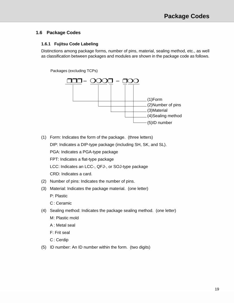
(1)Form(2)Number of pins(3)Material(4)Sealing method
(5)ID number
(1) Form: Indicates the form of the package. (three letters)
DIP: Indicates a DIP-type package (including SH, SK, and SL).
PGA: Indicates a PGA-type package
FPT: Indicates a flat-type package
LCC: Indicates an LCC-, QFJ-, or SOJ-type package
CRD: Indicates a card.
(2) Number of pins: Indicates the number of pins.
(3) Material: Indicates the package material. (one letter)
P: Plastic
C : Ceramic
(4) Sealing method: Indicates the package sealing method. (one letter)
M: Plastic mold
A : Metal seal
F: Frit seal
C : Cerdip
(5) ID number: An ID number within the form. (two digits)
1.6 Package Codes
1.6.1 Fujitsu Code Labeling
Distinctions among package forms, number of pins, material, sealing method, etc., as wellas classification between packages and modules are shown in the package code as follows.
Packages (excluding TCPs)
Package Codes

20
(4) Sealing method: Indicates the package sealing method. (one letter)
M: Resin sealed
B: Not sealed
(5) ID number: An ID number within the form. (two digits)
Package Codes
Packages (TCP)
– –
(1) Tape form(2)Number of outer leads(3)Tape format(4)Sealing material
(5)ID number
(Dimensions in mm)
(1) Tape form: Indicates the tape form of the package. (three letters)
DTP: TCP with leads on two sides
QTP: TCP with leads on four sides
(2) Number of outer leads: Indicates the number of outer leads that are actually used.
(3) Tape format: Indicates the tape format. (a letter from A to F)
a
34.975
48.175
66.800
34.975
48.175
69.950
b
4.750
4.750
4.750
4.750
4.750
4.750
c
1.420
1.420
1.420
1.981
1.981
1.981
e
31.820
44.860
66.800
28.977
42.177
63.949
d
1.420
1.420
1.420
1.981
1.981
1.981
Letter in
code
A
B
C
D
E
F
Symbol
35 mm superwide
48 mm superwide
70 mm superwide
35 mm wide
48 mm wide
70 mm wide
Name
c
d
b
ea
21
Package Codes
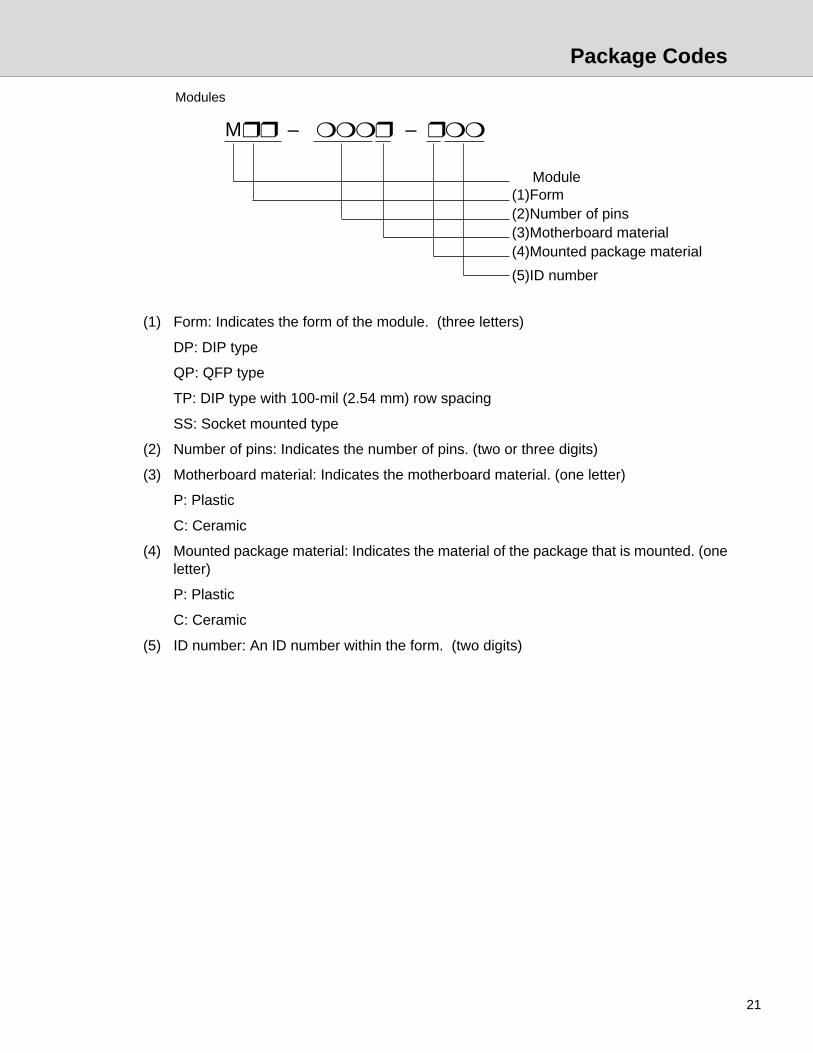
Modules
M – –
(1)Form(2)Number of pins(3)Motherboard material(4)Mounted package material
(5)ID number
(1) Form: Indicates the form of the module. (three letters)
DP: DIP type
QP: QFP type
TP: DIP type with 100-mil (2.54 mm) row spacing
SS: Socket mounted type
(2) Number of pins: Indicates the number of pins. (two or three digits)
(3) Motherboard material: Indicates the motherboard material. (one letter)
P: Plastic
C: Ceramic
(4) Mounted package material: Indicates the material of the package that is mounted. (oneletter)
P: Plastic
C: Ceramic
(5) ID number: An ID number within the form. (two digits)
Module

22
Package Codes
1.6.2 EIAJ code labeling
Section 1.6.1 explained the codes used by Fujitsu. This section explains the EIAJ codes.
(1) Special features concerning the exterior of the package
*: Standard package
S: Standard package with compressed lead pitch
H: Package with heat sink
W: Package with transparent window
A: Piggyback package
T: Package with a mounting height of 1.27mm (0.050 inches) or less
(2) Package name
Indicates either SIP, ZIP, DIP, PGA, SOP, SOL, SOJ, QFP, QFJ, or QFN.
(3) Number of pins on package
Basically indicates the total number of pins present. If the number of pins is 1000 ormore, four digits are used.
(4) Material and main characteristics of body of package
C: Airtight ceramic package sealed with metal
G: Airtight ceramic package sealed with glass
P: Package formed of resin
R: Package formed from plastic and glass compound substrate
X: Package not covered by any of the other designations
– – –
(1) Special features concerning the exterior of the package(2) Package name(3) Number of pins on package(4) Material and main characteristics of body of package(5) Reference dimensions of package
ID number

23
(5) Package reference dimensions
DIP: Package pin row spacing (unit: mil)
PAG: Refer to the following example:
S: SquarePin matrix (unit: example)Chip mounting positionU: Cavity Up
D: Cavity Down
Cavity up: The chip mounting position is on the top of the package
Cavity down: The chip mounting position is on the bottom of the package
SOP: Spacing between centers of mounting pads (unit: mil)
SOP/SOJ: Width of package body (unit: mil)
QFP: Size of package body (unit: mm)
QFJ, QFN: Refer to the following example:
FormS: SquareR: RectangleSize of package body (unit: mil)• Indicates the short side if the package is
rectangular.• If the size of the package body is four
digits or more, the three high-order digitsare used.
Package Codes
Example: S IO U
Example S 350

24
F JAPAN
MBxxxx
9850 E00
Marking
1.7 Marking
Marking includes Fujitsu’s standard marking and customer-specified marking. Section 1.7.1shows the format for standard marking; if customer-specified marking is desired, the customershould establish the marking specifications while observing the restrictions shown in section1.7.2 Note that in the case of customer-specified marking, the Engineering Samples (ES) willbear the standard marking, and the Commercial Samples (CS) will bear the customer-specifiedmarking.
If a format other than those shown in this data book is desired, consult with the Fujitsu salesoffice beforehand.
1.7.1 Standard marking
Information marked
F ........................ Fujitsu’s mark
JAPAN............... Country of manufacture
MBxxxx.............. Fujitsu product name
98 50 (Example) Lot No.
Code for week of IC manufacture: “01” indicates the first week, “02” the second week,and so on, up to “50”, which indicates the 50th week.
Code for year of IC manufacture: The last two digits of the year are shown. For 1990: “90”; for 1998: “98”.
<<Type 1>>
F MBxxxx
JAPAN 9850 E00
<<Type 2>>
Note: The <<Type 1>> and <<Type 2>> formats are the basic formats; there are othersimpler formats based on the lot number and control number for cases wherespace is limited, etc.

25
Marking
However, the lot number indication in the case of hybrid ICs is as follows.
IX 03 (Example)
Manufacturing serial number (count of lots for this month)
Code for month of manufacture: 1 to 9: January to September;X: October; Y: November; Z: December
Code for year of manufacture: Last digit of year
E01 (Example) .. Fujitsu’s control number

26
F MBxxxxx
JAPAN 9850 E00
>>>>>>>>
1.7.2 Customer-specified marking
If needed for custom ICs, etc., marking can be specified as indicated below.
Marking format
(1) One line for the customer product name (the customer part number) can be added toFujitsu’s standard marking format.
(2) Fujitsu’s mark can be replaced with the customer’s company mark.
If the customer’s company mark is to be required, a camara-ready copy must be submitted.
If marking other than that described above is desired, or if the above format is not feasible dueto space limitations, etc., special consultation will be necessary.
Note that the lot number and control number are administrative numbers required byFujitsu’s specifications, and cannot be omitted.
> > >Customer product name
(Customer part number)
F JAPAN
MBxxxxx
9850 E00
>>>>>>>>
Marking
27
1.8 Future Trends in Packages
1.8.1 Diversification
Semiconductor packages can be broadly classified into two types: pin inserted types andsurface mounted types. The main package format has changed from DIP to types such asSOP, QFP, and PGA. In addition, a package is now expected to provide the followingfeatures:
• High-density mounting in order to permit lighter and smaller designs as moreequipment becomes portable
• Multiple I/O pins, required as devices are integrated on larger scales and morefunctions are offered
• Faster speed
• Lower cost
Given the balance between mounting technology and the design standards for thereference printed circuit board that serves as the mounting platform, progress in the area ofsurface mounting and leadless packages (except for vertical packages) should beattainable.
Development is already progressing on representative types such as BGAs and CSPs. Thefeatures of each of these types and their future direction of development are describedbelow:
• SOPs are mainly suited for packages with up to 100 pins. There are versions in whichthe pitch is even smaller or the package profile is even lower, such as TSOPs andUTSOPs, and the trend is towards CSPs. One variation is the SVP, as progress inutilizing all three dimensions is made in order to permit high-density mounting ofmemory.
• QFP normally have from 50 to 300 pins.Packages for an even smaller pitch are inprogress and being deployed into QTPs and TPQFPs using tape carriers.
• PGAs are a package type suited for ICs with a large number of pins (200 to 500 pins).SPGAs offer an even narrow pitch, and BGAs are being developed for the future.
1.8.2 Future formats
In the future, due to the demand for high-density mounting, surface mounted packages willgrow in number, while the demand for higher speeds will drive the growth of leadlesspackages.
Cost requirements will cause growth in plastic packages, while the characteristics ofceramic packages will make them required for applications that demand high reliability, fordevices that operate at high speeds and consume a lot of power, and for large chips.
With these trends in mind, Fujitsu's own package development efforts will continue toemphasize mounting efficiency while paying attention to the need for compatibility with theJEDEC*1 standards, the EIAJ*2 standards, and packages from other manufacturers.
*1:Joint Electron Device Engineering Council
*2:Electronic Industries Association of JAPAN
Future Trends in Packages
28
1.8.3 Custom packages
In addition to the increasingly important diversity of product types, there is also a growingtrend towards diversity among semiconductor types and mounting methods. As amanufacturer of ASICs, it is important for Fujitsu to be able to quickly grasp market trendsand make strategic contributions to customer product differentiation efforts.
At Fujitsu, in addition to promoting new standard packages in order to meet market demandfor smaller and thinner packages, through joint development of CSPs and BGAs, we arealso striving to supply "user-friendly" custom packages that satisfy the needs of a singlecustomer. We make every effort to meet with customers and discuss in detail their desiresconcerning the form of the package, the dimensions, the number of leads, the exteriorprocessing, etc., and then we strive to meet those needs quickly and flexibly.
1.8.4 Modules
Recently, modules intended for higher densities and more advanced functions arebecoming increasingly important for the following types of applications:
• Although there is a trend towards combining multiple ICs and peripheral componentsinto a single LSI in order to raise mounting density and permit more sophisticatedfunctions, when the characteristics of the devices make it difficult to do so, a moduleis used to create a circuit block.
• High-density modules, such as PC cards, are used to increase mounting densities.
In light of these needs, and given our background in a variety of device families and smallpackage series, Fujitsu is devoting tremendous effort to the design and supply of modulesthat are suited for COB mounted (including multi-layered wiring boards) and surfacemounted packages.
1.8.5 Multi-chip Modules
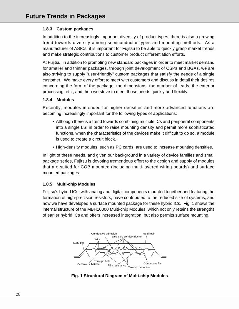
Fujitsu's hybrid ICs, with analog and digital components mounted together and featuring theformation of high-precision resistors, have contributed to the reduced size of systems, andnow we have developed a surface mounted package for these hybrid ICs. Fig. 1 shows theinternal structure of the MBH10000 Multi-chip Modules, which not only retains the strengthsof earlier hybrid ICs and offers increased integration, but also permits surface mounting.
Fig. 1 Structural Diagram of Multi-chip Modules
Lead pinWire
Conductive adhesiveBare chip semiconductor
Mold resin
Conductive filmCeramic capacitor
Film resistance
Through holeCeramic substrate
Future Trends in Packages

31
Overview
2.1 OverviewThere are two basic methods for mounting packages. One is the flow soldering method, and
the other is the reflow soldering method.
The flow soldering method, which is widely used for lead inserted type packages, uses a jet-
type solder bath to mount packages on printed circuit boards.
As electronic devices become smaller and lighter, IC packages are also expected to
become smaller and thinner. As a result, in recent years there has been rapid growth in
surface mounted packages, and surface mounting technology based on the reflow soldering
method has garnered much attention.
One point that is important is that the flow soldering method used with lead insertion
packages does not subject the package to much thermal stress, while in the reflow soldering
method used with surface mounted packages, the package as a whole is heated, so that
there is a great deal of thermal stress placed on the package, which must be noted during
mounting.
This chapter will provide an overview of the mounting methods, the level of package
moisture absorption, and the proper handling of packages, all in order to permit surface
mounted packages to be mounted in a proper manner that preserves their reliability.

32
Mounting Methods
2.2 Mounting Methods
2.2.1 Lead inserted type
There are two methods for mounting lead inserted type packages on a printed circuit board:
one method where the solder is applied directly to the printed circuit board, and another
method where the package is mounted in a socket on the board.
When applying solder directly to the board, the leads are inserted into the mounting holes in
the printed circuit board first, and the flow soldering method (wave soldering method) is used
with jet solder. This is the most popular and widely used method for mounting packages on
a printed circuit board.
However, during the soldering process, heat in excess of the normal maximum rating for the
storage temperature is applied to the leads. As a result, quality assurance concerning heat
resistance during soldering limits the soldering process to the levels shown below; do not
exceed these levels during soldering work.
1) Solder temperature and immersion time
260 °C (500 °F), 10 seconds or less
2) Lead immersion position
Up to a distance of at least 1 to 1.5 mm from the main body of the package
3) When mounting an element using the solder flow method, ensure that the element
itself is not immersed in the solder.
4) When using flux, avoid chlorine based fluxes; instead, use a resin-based flux.
Note, however, that if the module leads are exposed to the solder for a long period of time,
solder on the module board may melt and previously mounted ICs may become detached.
Also be careful to prevent any solder from coming into direct contact with the packages
mounted on the module.
When using socket mounting, in some cases when the surface treatment of the socket pins
is different from the surface metal of the IC leads, problems due to poor contact may arise.
Therefore, a check of the surface treatment of the socket contacts and of the surface
treatment of the IC leads is recommended.

33
Mounting Methods
2.2.2 Surface mounted typeCompared to the lead inserted type, surface mounted packages have finer, thinner leads,
which means that the leads are more easily bent. In addition, as packages come to have
more and more pins, the lead pitch is becoming narrower, making handling more difficult.
When the pitch of an IC is narrow, problems such as open pins caused by bent leads or short
circuits caused by solder bridges occur easily; therefore, suitable mounting technology
becomes a necessity.
Surface mounted packages include ceramic LCCs with no leads, flat packages with gull-
wing leads or straight leads, packages with J-leaded, and ball-grid array packages(BGA);
aside from the LCCs, the packages can be either plastic or ceramic. In the case of surface
mounted packages, the solder reflow method is recommended as the mounting method for
either type of package.
Fig. 1 illustrates the basic process for mounting.
Fig. 1 Flow Chart of Basic Mounting Process
Boards
(1) Solder paste application
Component
(2) Component preprocessing (baking, preliminary soldering)
(3) Component placement
(4) Solder reflow
(5) Cleaning/drying
Visual check/testing
There are a variety of methods for soldering surface mounted packages onto a printed
circuit board. Some of these methods are described below.
The mounting methods can be broadly classified into two types: partial heating methods and
the total heating methods. The partial heating methods are desirable from a reliability
standpoint since the thermal stress is small, but from the standpoint of mass production
such methods are somewhat more difficult to implement.
34
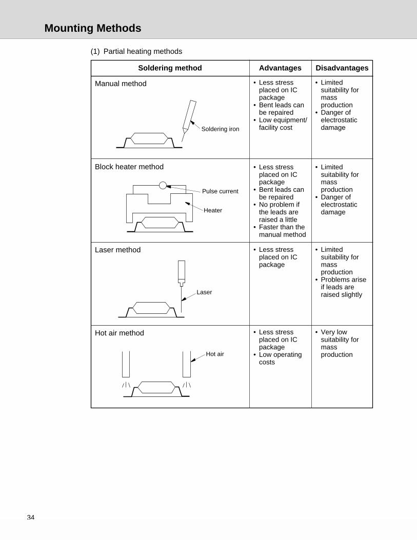
(1) Partial heating methods
Soldering method Advantages
• Less stressplaced on ICpackage
• Bent leads canbe repaired
• Low equipment/facility cost
• Less stressplaced on ICpackage
• Bent leads canbe repaired
• No problem ifthe leads areraised a little
• Faster than themanual method
• Less stressplaced on ICpackage
• Less stressplaced on ICpackage
• Low operatingcosts
Disadvantages
• Limitedsuitability formassproduction
• Danger ofelectrostaticdamage
• Limitedsuitability formassproduction
• Danger ofelectrostaticdamage
• Limitedsuitability formassproduction
• Problems ariseif leads areraised slightly
• Very lowsuitability formassproduction
Manual method
Block heater method
Laser method
Hot air method
Soldering iron
Pulse current
Heater
Laser
Hot air
Mounting Methods

35
(2) Total heating methods
Soldering method Advantages
• Highly suitedfor massproduction
• Existingtechniques andfacilities can beused
• Low operatingcosts
• Highly suitedfor massproduction
• Low operatingcosts
• Highly suitedfor massproduction
• Placescomparativelylittle stress onpackage
• Uniformity oftemperaturedistribution isexcellent
• Placescomparativelylittle stress onpackage
• Highly suitedfor massproduction
• Hightemperaturesare not applieddirectly to thepackage
Disadvantages
• Places themost stress onpackage
• Placescomparativelylarge amount ofstress onpackage
• Operatingcosts are high
• Oxidation dueto surroundingair may occur
• Cannot beused withdouble-sidedboards
Full dip method
Infrared reflow method
Vapor phase reflow method
Hot air heating method (used with far infrared
heat)
Underside heating method
Melted solder
Infrared heater
Saturated steam
Inert liquid(florinate)
Heater
Far infrared heater
Forced convection
Heater
Conveyor belt
Mounting Methods

36
Mounting Methods
2.2.3 Precautions on mounting
Points of consideration concerning mounting work are explained below.
(1) Boards
Packages can be mounted on a variety of boards, including resin boards made of materials
such as paper phenol or glass epoxy, ceramic boards, and flexible printed circuit boards,
and when selecting the board material it is essential to give due consideration to factors
such as matching the thermal expansion coefficients of the components to be mounted,
electrical and mechanical characteristics, heat dissipation characteristics, the total reliability
level, and cost. In addition, the reliability and production yield in terms of the wiring pattern
on the component mounting surface also become important factors.
Figs. 2, 3, and 4 show examples of design criteria for surface patterns. In the design stage,
consideration should be given to ease of mounting, reliability of the connections, pattern
spacing, and the possibility of solder bridge formation.
Fig. 2 Example of Surface Pattern Design Criteria for QFJs (SOJs)
QFJ
(lead wire)
L (pattern length)
P (lead pitch)
w (lead width)
W (pattern length)
L ≥w ≤ W ≤ P–0.30mm
Also applicable to SOJ.

37
Mounting Methods
Fig. 3 Example of Surface Pattern Design Criteria for SOPs and QFPs
Fig. 4 Example of Surface Pattern Design Criteria for LCCs
P
L ≥ + 0.70mm
w ≤ W ≤ P– 0.30mmAlso applicable to SOP.
W
QFP
w
L
0.50mm 0.20mm
2°
w ≤ W ≤ P * 0.6 for package with a pitch of 0.5 mm or less.
LCC
L (pattern length)
w (pad length)
W (pattern width)
P (pad pitch)
(pad length)
0.20
L ≥ + 0.20mm
w ≤W ≤ P–0.30mm

38
Mounting Methods
(2) Applying solder paste
There are two methods for supplying the solder paste: by printing and by dispenser.
When done by printing, a stainless steel screen mask is used to apply the solder paste.
When mounting packages with a narrow pitch, how the solder paste printing process is
performed has a major effect on the production yield after the reflow process, so careful
attention must be paid to the selection of the equipment and to the printing conditions.
Careful attention must also be paid to the selection of the solder paste and the printing
mask.
If the board surface is not flat and some of the solder is to be applied after a portion of the
components have already been mounted, the remaining solder paste can be applied by
using a dispenser.
(3) Solder paste
The solder paste is a mixture of solder powder (normally #250 to 325) mixed with flux.
The merits of using solder paste include:
• It is easy to control the amount of solder used.
• It is possible to use the viscosity of the paste to temporarily hold components in
place.
• There are no impurities from a solder bath, etc.
• It is well suited for automation and mass production.
The most common type of solder is lead-tin eutectic type, but when soldering boards or
components that use silver-lead for conductors, a eutectic type solder with a silver content of
about 2% or 3% is used.
Until now, most solder pastes have used a resin-type flux, but recently measures to
eliminate fluorocarbons and regulations on organic solvents have spurred the development
of pastes that require no cleaning process or that use water-soluble flux.
Key points to consider in the selection of flux include:
a) Selection based on catalog values
• Size and shape of the solder powder
• Solder composition
• Amount of flux and chlorine included
39
Conditions
100 °C (212 °F) to 150°C (302 °F)
260°C max. (500°F max.), 10 seconds max.
Natural cooling until temperature drops below 100°C (212 °F)
Mounting Methods
b) Evaluation criteria for actual trials
• Good patterning characteristics (deposits well)
• No change in the viscosity and uniformity of the mixture of solder powder and flux
over time
• Continuous printing possible
• Very little dripping or formation of solder balls when melted
• Easy to clean, with little flux residue, no-discoloration or staining
Although the cost of the solder paste is also important, the total manufacturing cost in terms
of production yield, etc., must be taken into consideration when selecting a paste, not just
the cost of the paste itself.
Before beginning mass production, a thorough study should be conducted and then those
materials that best fit the conditions under which they will be used should be selected.
Solder paste is normally applied through a printing process, using a screen mask about 150
µm thick.
(4) Component preprocessing
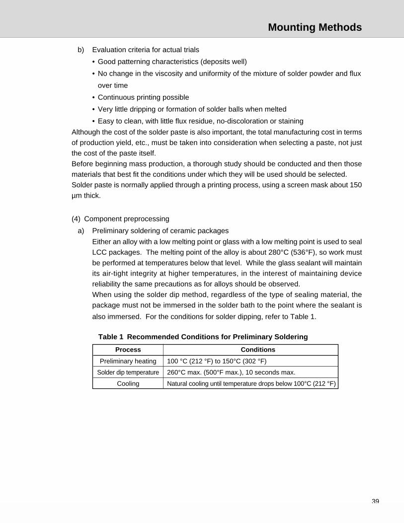
a) Preliminary soldering of ceramic packages
Either an alloy with a low melting point or glass with a low melting point is used to seal
LCC packages. The melting point of the alloy is about 280°C (536°F), so work must
be performed at temperatures below that level. While the glass sealant will maintain
its air-tight integrity at higher temperatures, in the interest of maintaining device
reliability the same precautions as for alloys should be observed.
When using the solder dip method, regardless of the type of sealing material, the
package must not be immersed in the solder bath to the point where the sealant is
also immersed. For the conditions for solder dipping, refer to Table 1.
Table 1 Recommended Conditions for Preliminary Soldering
Process
Preliminary heating
Solder dip temperature
Cooling

40
b) Baking plastic SMD packages
Unlike ceramic packages, plastic packages absorb moisture when exposed toatmosphere. Although this does not present a reliability problem during storage, if aplastic package that has absorbed moisture is soldered by the reflow method, thepackage may crack. Although it depends on the package type and the reflow method,it is important to note that some packages must undergo a baking process before thereflow process. (For details, refer to section 2.3, "Surface Mounted Plastic PackageReliability.")
(5) Component placementEquipment that positions surface mounted package components is available from a varietyof manufacturers in worldwide. When selecting such equipment, it is necessary to considerthe number of components it will handle and the manner in which the components arepackaged (in containers, trays, or on tape).Because the leads on flat packages extend outwards, they are easily bent. Because repairis difficult once the leads are bent, great care must be taken when handling the packages.
(6) Full solder dip (wave soldering method)
When using the full solder dip method for mounting, observe the following conditions.
(Contact a Fujitsu sales representative for details on those packages and products for which
full solder dipping is available.)
Solder bath temperature: 260°C max. (500°F max.)
Time: Less than 5 seconds
(7) Solder reflowThe typical reflow methods are: a) infrared reflow; b) vapor phase reflow; and c) hot airreflow. General descriptions ofeach of these methods are provided below. Note that the use of full solder dipping should beavoided.
a) Infrared reflow
This reflow method uses radiant heat from an infrared heater.
Advantages • Processing capability is high.• Temperature profile can be controlled comparatively well.• Operating cost is low.• Equipment is inexpensive.
Disadvantages • Temperature differences can arise due to differences in radiationabsorption rates on the board.
• Caution is required, since the flux is easily blackened.• Reflow in a normal oxidizing atmosphere.
b) Vapor phase reflow
This reflow method uses the latent heat of vaporization of an inert liquid.
Advantages • Uniform temperature distribution.
• Reflow in an inert atmosphere.
• No fear of overheating. (Heat is not applied above the boiling point of
the inert liquid.)
Mounting Methods

41
(a)
(b) (c)
(d)
(d')
(e)RT
150°C
210°C
240°C
Disadvantages • Temperature profile is limited.
• Operating cost is high.
• Processing capability decreases somewhat.
• Attention must be paid to ventilation.
• Equipment is expensive.
c) Hot air reflow
This reflow method uses convective thermal propagation with heat-saturated air.
There are two different types of methods: the far infrared combination type and the
hot air circulation type.
Advantages • Temperature profile can be controlled comparatively well.
• Temperature distribution can be made relatively uniform.
• Operating cost is low.
Disadvantages • Reflow in a normal oxidizing atmosphere.
• Processing capability decreases somewhat.
• Note on temperature profiles
No problems should arise if the temperature profile is equivalent to that of infrared reflow.
• Temperature profile for infrared reflow scheme
Mounting Methods
(a) Temperature increase gradient 1°C to 4°C /sec (33.8°F to 39.2°F /sec)
(b) Preliminary heating Temperature:150 ± 10°C (302 ± 50°F):60 sec or more
(c) Temperature increase gradient 1°C to 4°C /sec (33.8°F to 39.2°F /sec)
(d) Actual heating Temperature: 230°C (446°F) max.
Time: 10 sec or less
(Temperature of the top of the package
body)
(d') Temperature: 210°C (410°F) Time: 40 sec or less
(e) Natural cooling or forced cooling

42
Mounting Methods
• Temperature profile for infrared reflow scheme
230 °C
150 °C
RT
(a)
(c)(b) (e)
(d)(a) Temperature increase gradient 1°C to 4°C /sec (33.8°F to 39.2°F /sec)
(b) Preliminary heating Temperature:150 ± 10°C (302 ± 50°F):60 sec or more
(c) Temperature increase gradient 1°C to 4°C /sec (33.8°F to 39.2°F /sec)
(d) Actual heating Temperature: 230°C (446°F) max.
Time: 10 sec or less
(Temperature of the top of the package
body)
(e) Natural cooling or forced cooling
• Temperature profile for infrared reflow scheme
(a) Temperature increase gradient 1°C to 4°C /sec (33.8°F to 39.2°F /sec)
(b) Preliminary heating Temperature:150 ± 10°C (302 ± 50°F):60 sec or more
(c) Temperature increase gradient 1°C to 4°C /sec (33.8°F to 39.2°F /sec)
(d) Actual heating Temperature: 225°C (437°F) max.
220°C (428°F) up
Time: 10 sec or less
(Temperature of the top of the package
body)
(e) Natural cooling or forced cooling
220 °C
150 °C
RT
(a)
(c)(b) (e)
(d)

43
• Temperature profile for vapor phase reflow scheme (using florinate or an equivalent)
(a) Temperature increase gradient 1°C to 8°C /sec. (33.8°F to 46.4°F /sec)
(b) Temperature: 200°C to (Typ: 215°C) (392°F to (Typ: 419°F))
Time: 30 to 60 sec.
(8) Manual soldering (partial heating method)
This method uses a soldering iron; soldering is done with the IC fixed in place by flux or
adhesive.
Conditions Temperature: 350°C max. (662°F max.)
Time: 3 seconds max./pin
(9) Cleaning
After soldering, clean away any flux residue.
If any flux left on the printed circuit board begins to absorb moisture, it can have a negative
impact on reliability due to degradation of the insulation resistance or corrosion of the leads
due to the chlorine component of the flux; therefore, cleaning is recommended. Refer to
Table 2 for details on the cleaning requirements.
The following cautions should be observed during cleaning:
a) Do not touch printed surfaces until the cleaning fluid dries.
b) When solder paste was used for mounting, solder balls may have formed, depending
on the paste type, paste quality, mounting conditions, etc.; therefore, pay attention to
the need to clean away any solder ball residue as well.
(a)
RT
200°C(392°F)
215°C(419°F)
(b)
T typ
Mounting Methods

44
Table 2 Plastic Package Cleaning Requirements
Note: Cleaning ceramic packages
Do not use ultrasonic cleaning to clean ceramic packages after mounting. Instead, use
hot water, boiling water, steam, etc., for cleaning. Also, caution should be exercised in
regards to the volatility of the cleaning fluids, and performing the work in sealed
equipment is recommended.
(8) Miscellaneous (reworking a package)
If, after mounting, a package must be reworked, use a hot jet or other method to apply
localized heat in order to remove the package in question, and then mount a proper package
in its place in the same manner. In this instance, the preliminary soldering method and the
solder paste (applied with a dispenser) method can be used individually or together. In
either case, keep the points described in item 4, "Component preprocessing," in mind. From
the standpoint of device reliability, such replacements should be kept to a minimum.
Frequency
Ultrasonic wave output
Solvent
Cleaning time
Cautions
27 to 29kHz
15w/s or less
Water-based cleaning solvent, alcohol-based
cleaning solvent, etc.
Up to 30 seconds (one time)
• The packages must not resonate.
• The packages and printed circuit board must
not come into direct contact with the vibration
source.
• Do not touch or brush printed surfaces while
cleaning is in progress or while there is
cleaning solvent on a package.
• When using solvents, observe public
environmental standards and safety
standards.
Mounting Methods
45
Surface Mounted Plastic Package Reliability
2.3 Surface Mounted Plastic Package Reliability
The heat stress that surface mounted plastic packages are subjected to when they are
mounted adversely affects their humidity resistance characteristics. This section describes
the humidity resistance characteristics of surface mounted plastic packages.
2.3.1 Features of surface mounted packages
Compared with conventional lead inserted types, surface mounted packages offer the
following advantages and disadvantages.
(1) Advantages
• Higher mounting densities are possible, making thinner and lighter devices
possible.
• Packages can have more pins.
• Surface mounted packages offer benefits from the standpoint of electrical
characteristics.
• Because through holes are not needed, costs are lower.
• Surface mounted packages are suited for automated assembly lines.
(2) Disadvantages
• Surface mounted packages are vulnerable to thermal stress during mounting,
which can result in cracked packages or poor humidity resistance characteristics.
• Because the external leads are thin, they are easily bent.
• Because the pitch is very small, solder bridges form easily.
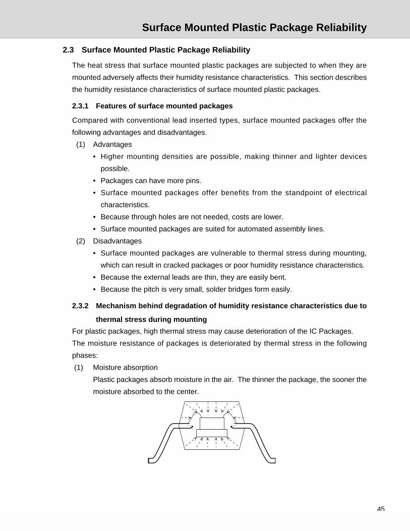
2.3.2 Mechanism behind degradation of humidity resistance characteristics due to
thermal stress during mounting
For plastic packages, high thermal stress may cause deterioration of the IC Packages.
The moisture resistance of packages is deteriorated by thermal stress in the following
phases:
(1) Moisture absorption
Plastic packages absorb moisture in the air. The thinner the package, the sooner the
moisture absorbed to the center.

46
(2) Thermal stress during mounting
The mounting temperature and time depend on the mounting method. In particular,
the overall heating method causes higher thermal stress on the package than the
partial heating method.
(3) Temperature increase in package
The increasing temperature causes evaporation of moisture absorbed in phase (1),
and deterioration of resin strength and mismatch between the lead frame and resin of
the package due to the different thermal expansion coefficients.
(4) Resin interface exfoliation
The stress generated in phase (3), causes exfoliation of the package resin interface.
(The water pressure increases to 46 atm at 260˚C (500 ˚F).)
Surface Mounted Plastic Package Reliability

47
(5) Package cracking
If the above-mentioned stress is high, package cracking and bonding wire breaking
may occur.
2.3.3 Measures to improve humidity resistance characteristicsIn response to the mechanisms described above that contribute to the degradation of a
package's humidity resistance characteristics, Fujitsu is taking the following measures in
order to improve reliability.
(1) Improvement of mold resins
Fujitsu is striving to improve the sealing power of resins, reduce the stress that they are
subjected to, and to increase their purity.
(2) Improvement of the lead frame
It is essential to eliminate the boundary surface separations that form due to thermal
expansion of the lead frame and the resin when thermal stress is applied during the
mounting process.
(3) Improvement of packaging materials for shipment
Since one of the mechanisms described was the absorption of moisture by plastic ICs
which in turn lead to a degradation of humidity resistance characteristics, Fujitsu
packages ICs in an aluminum-laminate pouch that is highly impermeable to moisture,
and with silica gel placed inside the pouch.
2.3.4 Mount ranking
Surface mounted plastic packages come in a variety of sizes and thicknesses, and also vary
in their ability to withstand the thermal stress of the mounting process. Therefore, Fujitsu
specifies (for each individual product) the number of days that can elapse between the time
a shipment of ICs is unpacked until the time when they are mounted. This specification is
called the "mount ranking." The number of days allowed differs according to the product
name, the package, and the mounting conditions. Table 3 shows classified mount ranking.
Even for the same packages, the mounting rank may vary depending on the device
type.For detailed information about each mounting rank, contact Fujitsu.
Surface Mounted Plastic Package Reliability

48
Table 3 Classification of Mounting Ranks (Mounting by Overall Heating)
gnippidllarevO gnippidllarevO gnippidllarevO gnippidllarevO gnippidllarevO *RI *RI *RI *RI *RI 11111 semit2xRI semit2xRI semit2xRI semit2xRI semit2xRI *SPV *SPV *SPV *SPV *SPV 22222
knargitnuoM
A )noitcudorpretfasraey2nihtiw(eerF
B *BPretfasyad7nihtiW 3 52nihtiWsyad
*syad41nihtiW 4 52nihtiWsyad
Cn elbissopmI
nnihtiWsyad
n ≥ 01syad7nihtiW
nnihtiWsyad
nnihtiWsyad
n>01 ≥ 7syad3nihtiW
nnihtiWsyad
0>n>7elbissopmI
Dn elbissopmI elbissopmI elbissopmInnihtiW
syad
Fn elbissopmInnihtiW
syad
n ≥ 01syad7nihtiW
nnihtiWsyad
n>01 ≥ 7syad3nihtiW
0>n>7elbissopmI
Jn elbissopmInnihtiW
syadelbissopmI
nnihtiWsyad
n: Number of days (for control of moisture absorption)
*1: Infrared reflow
Peak temperature A, B, Cn : 240˚C (464˚F) Max. within 10 min.
Fn : 230˚C (446˚F) Max. within 10 min.
Jn : 225˚C (437˚F) Max. (conforms with JEDEC)
*2: Vapor phase soldering
*3: Overall dip is possible depending on products or packages.
Mounting by overall dipping requires baking at 125˚C (257˚F) for 24 H.
*4: Double reflow is not supported for some products or packages. (QFJ22, etc.)
• Mounting by partial heating
Mounting by partial heating is possible at any rank (A to D).
Surface Mounted Plastic Package Reliability
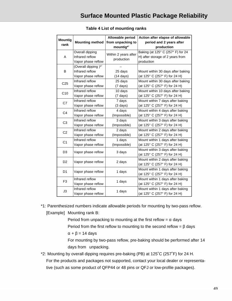
49
Table 4 List of mounting ranks
gitnuoMknar
dohtemgnitnuoMdoirepelbawollAotgnikcapnumorf
*gitnuom 1
elbawollafoespaleretfanoitcAretfasraey2dnadoirep
noitcudorp
AgnippidllarevO
wolferderarfnIwolferesahpropaV
retfasraey2nihtiWnoitcudorp
521ta(gnikaB ° 752(C ° 42rof)Fmorfsraey2foegarotsretfa)H
noitcudorp
B*)gnippidllarevO( 2
wolferderarfnIwolferesahpropaV
–syad52)syad41(
gnikabretfasyad03nihtiwtnuoM521ta( ° 752(C ° )H42rof)F
52CwolferderarfnI
wolferesahpropaVsyad52)syad7(
gnikabretfasyad03nihtiwtnuoM521ta( ° 752(C ° )H42rof)F
01CwolferderarfnI
wolferesahpropaVsyad01)syad7(
gnikabretfasyad01nihtiwtnuoM521ta( ° 752(C ° )H42rof)F
7CwolferderarfnI
wolferesahpropaVsyad7)syad3(
gnikabretfasyad7nihtiwtnuoM521ta( ° 752(C ° )H42rof)F
4CwolferderarfnI
wolferesahpropaVsyad4
)elbissopmI(gnikabretfasyad4nihtiwtnuoM
521ta( ° 752(C ° )H42rof)F
3CwolferderarfnI
wolferesahpropaVsyad3
)elbissopmI(gnikabretfasyad3nihtiwtnuoM
521ta( ° 752(C ° )H42rof)F
2CwolferderarfnI
wolferesahpropaVsyad2
)elbissopmI(gnikabretfasyad2nihtiwtnuoM
521ta( ° 752(C ° )H42rof)F
1CwolferderarfnI
wolferesahpropaVsyad1
)elbissopmI(gnikabretfasyad1nihtiwtnuoM
521ta( ° 752(C ° )H42rof)F
3D wolferesahpropaV syad3gnikabretfasyad3nihtiwtnuoM
521ta( ° 752(C ° )H42rof)F
2D wolferesahpropaV syad2gnikabretfasyad2nihtiwtnuoM
521ta( ° 752(C ° )H42rof)F
1D wolferesahpropaV syad1gnikabretfasyad1nihtiwtnuoM
521ta( ° 752(C ° )H42rof)F
3FwolferderarfnI
wolferesahpropaVsyad1
gnikabretfasyad1nihtiwtnuoM521ta( ° 752(C ° )H42rof)F
3JwolferderarfnI
wolferesahpropaVsyad1
gnikabretfasyad1nihtiwtnuoM521ta( ° 752(C ° )H42rof)F
*1: Parenthesized numbers indicate allowable periods for mounting by two-pass reflow.
[Example] Mounting rank B:
Period from unpacking to mounting at the first reflow = α days
Period from the first reflow to mounting to the second reflow = β days
α + β = 14 days
For mounting by two-pass reflow, pre-baking should be performed after 14
days from unpacking.
*2: Mounting by overall dipping requires pre-baking (PB) at 125˚C (257˚F) for 24 H.
For the products and packages not supported, contact your local dealer or representa-
tive (such as some product of QFP44 or 48 pins or QFJ or low-profile packages).
Surface Mounted Plastic Package Reliability

50
2.3.5 Storage and drying processing
Surface mounted plastic packages should be stored while still packed in the materials that
they were shipped in from Fujitsu. If you have any questions, contact Fujitsu.2.3.6 Reliability dataBecause surface mounted plastic packages are mounted by total heating methods, they are
easily affected by thermal stress during the mounting process, with the result that packages
sometimes crack or their humidity resistance characteristics are adversely affected.
In addition to normal reliability evaluations, Fujitsu subjects SMDs to temperature cycle tests
and PTHS tests after preprocessing the packages for solder heat resistance, all in order to
evaluate reliability versus the stresses encountered during the mounting process.
Tables 5 to 9 show examples of the results of these evaluations.
Table 5 Reliability Testing Results (SOJ-42P MB81V16160A)
metitseT snoitidnoctseT stlusertseTegarotserutarepmethgiH
tset051 _ 203(C _F)
H000155/0
erutarepmethgiH*tsetnoitareposuounitnoc
)noitarepoCA(
521 _ 752(C _F)H0001
501/0
erutarepmethgiH*tsetnoitareposuounitnoc
)noitarepoCD(
051 _ 203(C _F)H0001
55/0
suounitnocytidimuhhgiH*tsetnoitarepo)noitarepoCA(
58 _ 581(C _ )F %58/H0001
55/0
erutarepmetwoLtsetnoitareposuounitnoc
)noitarepoCA(
55– _ 76–(C _ )FH0001
55/0
*elcycerutarepmeT56– _ 051otC _C58–( _ 203otF _ )F
C00155/0
kcohslamrehT0_ 001otC _C23( _ 212otF _ )F
C00155/0
*SHTP121 _ 052(C _ )F %001/
H86155/0
BHTP121 _ 052(C _ )F %001/
H6952/0
* Preprocessing requirements: Drying 125˚C (257˚F), 24 H + humidity absorption precess
85˚C (185˚F)/ 85%, 48 H + Infrared reflow 245˚C (473˚F) Max.
Surface Mounted Plastic Package Reliability

51
Table 6 Reliability Testing Results (SON-40P MBM29LV004)
metitseT snoitidnoctseT stlusertseTegarotserutarepmethgiH
tset051 _ 203(C _ )F
H000152/0
erutarepmethgiH*tsetnoitareposuounitnoc
)noitarepoCA(
521 _ 752(C _ )FH0001
55/0
suounitnocytidimuhhgiH*tsetnoitarepo)noitarepoCA(
58 _ 581(C _ %58/)FH0001
52/0
*elcycerutarepmeT56– _ 051otC _C58–( _ 203otF _ )F
C001501/0
kcohslamrehT0_ 001otC _C23( _ 212otF _ )F
C00155/0
*SHTP121 _ 052(C _ %001/)F
H86155/0
BHTP121 _ 052(C _ %001/)F
H6952/0
* Preprocessing requirements: Drying 125˚C (257˚F), 24 H + humidity absorption precess
85˚C (185˚F)/85%, 6 H +Infrared reflow 245˚C (473˚F) Max.
Table 7 Reliability Testing Results (SSOP-20P MB15A60)
metitseT snoitidnoctseT stlusertseTegarotserutarepmethgiH
tset051 _ 203(C _ )F
H000152/0
erutarepmethgiH*tsetnoitareposuounitnoc
)noitarepoCA(
051 _ 203(C _ )FH0001
55/0
suounitnocytidimuhhgiH*tsetnoitarepo)noitarepoCA(
58 _ 581(C _ %58/)FH0001
52/0
erutarepmetwoLtsetnoitareposuounitnoc
)noitarepoCA(
55– _ 76–(C _ )FH0001
52/0
*elcycerutarepmeT56– _ 051otC _C58–( _ 203otF _ )F
C00155/0
kcohslamrehT0_ 001otC _C23( _ 212otF _ )F
C00152/0
*SHTP121 _ 052(C _ %001/)F
H86155/0
BHTP121 _ 052(C _ %001/)F
H6952/0
* Preprocessing requirements: Drying 125˚C (257˚F), 24 H + humidity absorption precess
85˚C (185˚F)/85%, 24 H + Infrared reflow 245˚C (473˚F) Max.
Surface Mounted Plastic Package Reliability

52
Table 8 Reliability Testing Results (QFP-120P MB90000A Serise)
metitseT snoitidnoctseT stlusertseTerutarepmethgiH
tsetegarots051 _ 203(C _ )F
H000155/0
erutarepmethgiHnoitareposuounitnoc)noitarepoCA(*tset
051 _ 203(C _ )FH0001
501/0
ytidimuhhgiHnoitareposuounitnoc
*tset)noitarepoCA(
58 _ 581(C _ %58/)FH0001
55/0
erutarepmetwoLnoitareposuounitnoc)noitarepoCA(tset
55– _ 76–(C _ )FH0001
52/0
*elcycerutarepmeT56– _ 051otC _C58–( _ 203otF _ )F
C001501/0
kcohslamrehT0_ 001otC _C23( _ 212otF _ )F
C00155/0
*SHTP121 _ 052(C _ %001/)F
H86155/0
BHTP121 _ 052(C _ %001/)F
H6952/0
* Preprocessing requirements: Drying 125˚C (257˚F), 24 H + humidity absorption precess
30˚C (86˚F)/85%, 96 H + Infrared reflow 245˚C (473˚F) Max.
Table 9 Reliability Testing Results (QFP-256P MBCE46194)
metitseT snoitidnoctseT stlusertseTerutarepmethgiH
tsetegarots051 _ 203(C _ )F
H000152/0
erutarepmethgiHnoitareposuounitnoc)noitarepoCA(*tset
001 _ 212(C _ )FH0001
55/0
ytidimuhhgiHnoitareposuounitnoc
*tset)noitarepoCA(
58 _ 581(C _ %58/)FH0001
52/0
erutarepmetwoLnoitareposuounitnoc)noitarepoCA(tset
55– _ 76–(C _ )FH0001
52/0
*elcycerutarepmeT56– _ 051otC _C58–( _ 203otF _ )F
C00155/0
kcohslamrehT0_ 001otC _C23( _ 212otF _ )F
C00152/0
*SHTP121 _ 052(C _ %001/)F
H86155/0
BHTP121 _ 052(C _ %001/)F
H6952/0
* Preprocessing requirements: Drying 125˚C (257˚F), 24 H + humidity absorption precess
30˚C (86˚F)/85%, 96 H + Infrared reflow 245˚C (473˚F) Max.
Surface Mounted Plastic Package Reliability

53
Table 10 Reliability Testing Results (BCC-16P MB15E07SL)
metitseT snoitidnoctseT stlusertseTerutarepmethgiH
tsetegarots051 ° 203(C ° )F
H000152/0
erutarepmethgiHnoitareposuounitnoc)noitarepoCA(*tset
051 ° 203(C ° )FD5001/H0001
55/0
ytidimuhhgiHnoitareposuounitnoc
*tset)noitarepoCA(
58 ° 581(C ° %58/)FH0001
52/0
erutarepmetwoLnoitareposuounitnoc)noitarepoCA(tset
55– ° 76–(C ° )FH0001
52/0
*elcycerutarepmeTC0101c002
55/0
kcohslamrehTA1101c002
52/0
*SHTP121 ° 052(C ° 30.2/)F
× 015
aPH861
55/0
BHTP121 ° 052(C ° 30.2/)F
× 015
aPH69
52/0
* Preprocessing requirements: Drying 125˚C (257˚F), 24 H + humidity absorption precess
85˚C (185˚F)/85%, 48 H + Infrared reflow 245˚C (473˚F) Max.
Table 11 Reliability Testing Results (FBGA-48P MBM29LV800A)
metitseT snoitidnoctseT stlusertseTerutarepmethgiH
tsetegarots051 ° 203(C ° )F
H000152/0
ytidimuhhgiHnoitareposuounitnoc
*tset)noitarepoCD(
58 ° 581(C ° %58/)FH0001
55/0
*elcycerutarepmeTC0101c002
501/0
kcohslamrehTA1101c002
55/0
*SHTP121 ° 052(C ° %58/)F
H86155/0
BHTP121 ° 052(C ° %58/)F
H6952/0
* Preprocessing requirements: Drying 125˚C (257˚F), 24 H + humidity absorption precess
85˚C (185˚F)/85%, 24 H + Infrared reflow 245˚C (473˚F) Max.
Surface Mounted Plastic Package Reliability
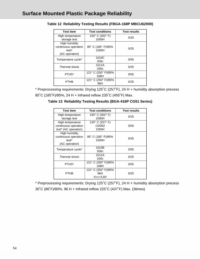
54
Table 12 Reliability Testing Results (FBGA-168P MBCU62000)
metitseT snoitidnoctseT stlusertseTerutarepmethgiH
tsetegarots051 ° 203(C ° )F
H000152/0
ytidimuhhgiHnoitareposuounitnoc
*tset)noitarepoCA(
58 ° 581(C ° %58/)FH0001
52/0
*elcycerutarepmeTC0101c002
55/0
kcohslamrehTA1101c002
52/0
*SHTP121 ° 052(C ° %58/)F
H86155/0
BHTP121 ° 052(C ° %58/)F
H6952/0
* Preprocessing requirements: Drying 125˚C (257˚F), 24 H + humidity absorption precess
85˚C (185˚F)/85%, 24 H + Infrared reflow 235˚C (455˚F) Max.
Table 13 Reliability Testing Results (BGA-416P CG51 Series)
metitseT snoitidnoctseT stlusertseTerutarepmethgiH
tsetegarots051 ° 203(C ° )F
H000152/0
erutarepmethgiHnoitareposuounitnoc)noitarepoCA(*tset
521 ° 752(C ° )FD5001/H0001
55/0
ytidimuhhgiHnoitareposuounitnoc
*tset)noitarepoCA(
58 ° 581(C ° %58/)FH0001
52/0
*elcycerutarepmeTB0101c005
55/0
kcohslamrehTA1101c002
52/0
*SHTP121 ° 052(C ° %58/)F
H86155/0
BHTP121 ° 052(C ° %58/)F
H69V CC V8.3=
52/0
* Preprocessing requirements: Drying 125˚C (257˚F), 24 H + humidity absorption precess
30˚C (86˚F)/80%, 96 H + Infrared reflow 225˚C (437˚F) Max. (3times)
Surface Mounted Plastic Package Reliability
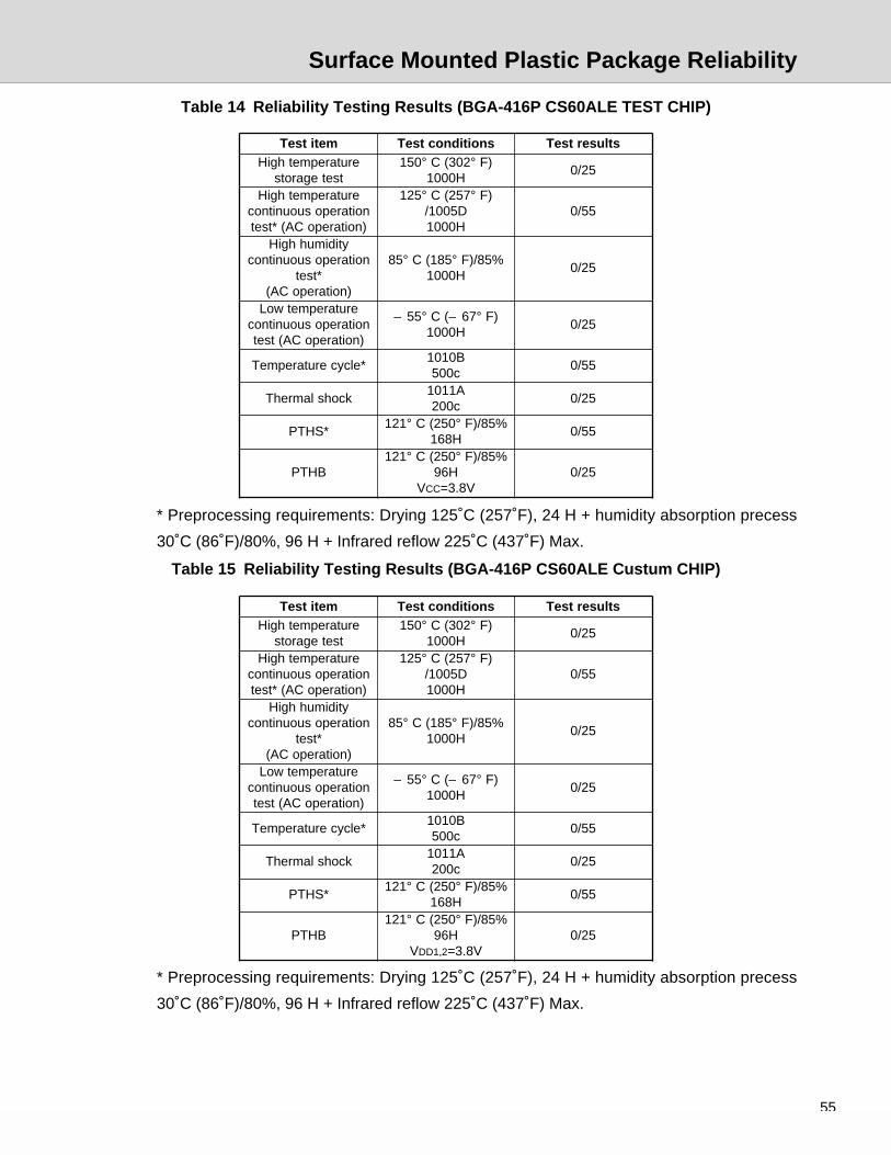
55
Table 14 Reliability Testing Results (BGA-416P CS60ALE TEST CHIP)
metitseT snoitidnoctseT stlusertseTerutarepmethgiH
tsetegarots051 ° 203(C ° )F
H000152/0
erutarepmethgiHnoitareposuounitnoc)noitarepoCA(*tset
521 ° 752(C ° )FD5001/H0001
55/0
ytidimuhhgiHnoitareposuounitnoc
*tset)noitarepoCA(
58 ° 581(C ° %58/)FH0001
52/0
erutarepmetwoLnoitareposuounitnoc)noitarepoCA(tset
55– ° 76–(C ° )FH0001
52/0
*elcycerutarepmeTB0101c005
55/0
kcohslamrehTA1101c002
52/0
*SHTP121 ° 052(C ° %58/)F
H86155/0
BHTP121 ° 052(C ° %58/)F
H69V CC V8.3=
52/0
* Preprocessing requirements: Drying 125˚C (257˚F), 24 H + humidity absorption precess
30˚C (86˚F)/80%, 96 H + Infrared reflow 225˚C (437˚F) Max.
Table 15 Reliability Testing Results (BGA-416P CS60ALE Custum CHIP)
metitseT snoitidnoctseT stlusertseTerutarepmethgiH
tsetegarots051 ° 203(C ° )F
H000152/0
erutarepmethgiHnoitareposuounitnoc)noitarepoCA(*tset
521 ° 752(C ° )FD5001/H0001
55/0
ytidimuhhgiHnoitareposuounitnoc
*tset)noitarepoCA(
58 ° 581(C ° %58/)FH0001
52/0
erutarepmetwoLnoitareposuounitnoc)noitarepoCA(tset
55– ° 76–(C ° )FH0001
52/0
*elcycerutarepmeTB0101c005
55/0
kcohslamrehTA1101c002
52/0
*SHTP121 ° 052(C ° %58/)F
H86155/0
BHTP121 ° 052(C ° %58/)F
H69V 2,1DD V8.3=
52/0
* Preprocessing requirements: Drying 125˚C (257˚F), 24 H + humidity absorption precess
30˚C (86˚F)/80%, 96 H + Infrared reflow 225˚C (437˚F) Max.
Surface Mounted Plastic Package Reliability

56
Table 16 Reliability Testing Results (TSOP-86P MB811643242A)
metitseT snoitidnoctseT stlusertseTerutarepmethgiH
noitareposuounitnoc)noitarepoCA(*tset
521 ° 752(C ° )FD5001/H0001
55/0
ytidimuhhgiHnoitareposuounitnoc
*tset)noitarepoCA(
58 ° 581(C ° %58/)FH0001
52/0
*elcycerutarepmeTC0101c002
501/0
kcohslamrehTA1101c002
55/0
*SHTP121 ° 052(C ° mta2/)F
H86155/0
BHTP121 ° 052(C ° mta2/)F
H6952/0
* Preprocessing requirements: Drying 125˚C (257˚F), 24 H + humidity absorption precess
85˚C (185˚F)/85%, 24 H + Infrared reflow 235˚C (455˚F) Max.
Surface Mounted Plastic Package Reliability
57
Storage
2.4 Storage
Products should be stored while still packed in the materials that they were shipped in from
Fujitsu.
• The recommended condition for the storage area is as belows;
Room Temperature; 5 to 30°C (41 to 86°F)
Room Humidity; 40 to 70%
• Do not store the products where they will be exposed to corrosive gases or in dusty
locations.
• Because sudden temperature changes can cause moisture to condense on the
products, store the products in an area where the temperature remains fairly constant.
• Note that if products are stored for an extended period of time, the solderability of the
lead pins may decline, rust may form, or the electrical characteristics may deteriorate.

Package Forms and Number of Pins
59
3.1 Package Forms and Number of Pins
The following tables show the correspondence between the forms and number of pins for eachpackage.
Lead inserted types
Form PackageNumber of pins
8 9 14 16 17 18 19 20 22 24 28 32 36 40 42 48 52 64 68 80 88 107 121 135 149 179 208 211 256 299 321 361 401 441
Standard DIP
Small
SH-
DIP
SK-
DIP
SL-
DIP
Matrix PGA
: Plastic : Ceramic
Package Forms and Number of Pins
60
Surface mounted types
Form Pack-age
Number of pins
8 14 16 18 20 24 28 30 32 34 38 40 44 48 50 54 56 64 68 80 86 100 104 120 124 144 160 164 168 176 196 208 216 232 240 256 260 296 304 320 368
Flat
SOP
SOL
SSOP
TSOP
CSOP
QFP
LQFP
TQFP
FPT
(round)
Form Pack-age
Number of pins
16 26 28 32 36 40 42 44 46 48 57 61 64 68 69 77 84 100 112 120 144 168 176 192 224 240 256 272 288 320 352 416 420 560 576 672 720 1196 1344 1600
Lead-less chip carrier
SON
BCC
QFN
PCLP
LCC
Leaded chip
carrier
QFJ
SOJ
Matrix
BGA
FBGA
T-BGA
: Plastic : Ceramic

Package Forms and Number of Pins
61
Modules, Cards Package Lineup
Mount type Form PackageNumber of pins
72 48 60 64 68 80 100 144 168 200
Modules
SMD
SIMM
MZIP
DIMM
Piggy back Flat
Cardss Socket
: Plastic : Ceramic
Package Lineup
62
3.2 Package Lineup
3.2.1 Lead inserted types
Plastic and Ceramic DIPs
(continued)
Number
of pinsForm Construction Package code
Lead pitchmm/mil
Row spacingmm/mil
Weight
g/packageFeatures
8 M DIP-8P-M01 2.54/100 7.62/300 0.45
14Stan-dard
M DIP-14P-M02 2.54/100 7.62/300 0.94 ( = M01) Index is different
CDIP-14C-C01 2.54/100 7.62/300 Pin length: 134mil,
package width: 248mil
DIP-14C-C04 2.54/100 7.62/300 Pin length: 134mil, package width: 268mil
16Stan-dard
M
DIP-16P-M03 2.54/100 7.62/300 1.07 Package width: 260mil
DIP-16P-M04 2.54/100 7.62/300 1.06 Package width: 244mil
DIP-16P-M05 2.54/100 7.62/300 1.06 Package width: 283mil
C
DIP-16C-C01 2.54/100 7.62/300 Package width: 248mil
DIP-16C-C02 2.54/100 7.62/300 Package width: 268mil
DIP-16C-C04 2.54/100 7.62/300 Package width: 288mil
18Stan-dard
M
DIP-18P-M02 2.54/100 7.62/300 1.16 Package width: 244mil
DIP-18P-M03 2.54/100 7.62/300 1.15 Package width: 260mil
DIP-18P-M04 2.54/100 7.62/300 1.31 Package width: 283mil
C DIP-18C-C01 2.54/100 7.62/300
20Stan-dard
M
DIP-20P-M01 2.54/100 7.62/300 1.22 Package width: 260mil
DIP-20P-M02 2.54/100 7.62/300 Package width: 244mil
DIP-20P-M03 2.54/100 7.62/300 1.53 Package width: 283mil
A DIP-20C-A01 2.54/100 7.62/300 Package width: 288mil, mounted height: 177mil
CDIP-20C-C01 2.54/100 7.62/300 Package width: 275mil
DIP-20C-C02 2.54/100 10.16/400 Package width: 380mil
22
Stan-dard
M DIP-22P-M03 2.54/100 10.16/400 1.94
C DIP-22C-C02 2.54/100 10.16/400
SKM DIP-22P-M04 2.54/100 7.62/300 1.41
C DIP-22C-C03 2.54/100 7.62/300
24Stan-dard
M DIP-24P-M02 2.54/100 15.24/600 3.40
A
DIP-24C-A04 2.54/100 15.24/600 Package width: 588mil, mounted height: 177mil, maximum pin width: 50mil
DIP-24C-A06 2.54/100 15.24/600 Package width: 590mil, mounted height: 200mil, maximum pin width: 40mil

Package Lineup
63
(continued)
(continued)
Number
of pinsForm Construction Package code
Lead pitchmm/mil
Row spacingmm/mil
Weight
g/packageFeatures
24
Stan-dard
A DIP-24C-A07 2.54/100 15.24/600 Package width: 595mil, mounted height: 177mil, maximum pin width: 40mil
CDIP-24C-C01 2.54/100 15.24/600 Package width: 520mil
DIP-24C-C03 2.54/100 15.24/600 Package width: 577mil
SH M DIP-24P-M05 1.778/70 7.62/300 1.15
SKM DIP-24P-M03 2.54/100 7.62/300 1.55
C DIP-24C-C04 2.54/100 7.62/300
SL
M DIP-24P-M04 2.54/100 10.16/400 2.35
A DIP-24C-A05 2.54/100 10.16/400 C DIP-24C-C05 2.54/100 10.16/400
28
Stan-dard
M DIP-28P-M05 2.54/100 15.24/600 ( = M02) Index is different
ADIP-28C-A01 2.54/100 15.24/600 Mounted height: 177mil
DIP-28C-A07 2.54/100 15.24/600 Mounted height: 200mil
C DIP-28C-C02 2.54/100 15.24/600 SH M DIP-28P-M03 1.778/70 10.16/400 1.87
SK M DIP-28P-M04 2.54/100 7.62/300 2.10
SLM DIP-28P-M06 2.54/100 10.16/400 A DIP-28C-A10 2.54/100 10.16/400
32
Stan-dard
M DIP-32P-M01 2.54/100 15.24/600 4.60
SK M DIP-32P-M02 2.54/100 7.62/300 2.45 Package length: 1600mil
SL A DIP-32C-A02 2.54/100 10.16/400
36Stan-dard
M DIP-36P-M01 2.54/100 15.24/600 5.36 Package length: 2063mil
40Stan-dard
M DIP-40P-M02 2.54/100 15.24/600 Package length: 1510mil
ADIP-40C-A04 2.54/100 15.24/600 With window(DIA : 355mil)
DIP-40C-A05 2.54/100 15.24/600 Purple body
SH M DIP-40P-M03 1.778/70 15.24/600 4.44
42Stan-dard
M DIP-42P-M03 2.54/100 15.24/600 ( = M01) Index is different
ADIP-42C-A01 2.54/100 15.24/600
DIP-42C-A03 2.54/100 15.24/600 ( = A01) With window (DIA : 335mil)
SH M DIP-42P-M02 1.778/70 15.24/600 4.47
48Stan-dard
M DIP-48P-M02 2.54/100 15.24/600 7.52
A DIP-48C-A01 2.54/100 15.24/600 SH M DIP-48P-M01 1.778/70 15.24/600 5.00
M : Plastic mold A : Metal seal (ceramic)F : Frit seal (ceramic) C : Cerdip(ceramic)

Package Lineup
64
(continued)
Ceramic PGAs
(continued)
Number
of pinsForm Construction Package code
Lead pitchmm/mil
Row spacingmm/mil
Weight
g/packageFeatures
52 SH M DIP-52P-M01 1.778/70 15.24/600 5.55
64 SH
M DIP-64P-M01 1.778/70 19.05/750 9.03
ADIP-64C-A02 1.778/70 19.05/750
DIP-64C-A06 1.778/70 19.05/750 ( = A02) With window (DIA : 350mil)
M : Plastic mold A : Metal seal (ceramic)F : Frit seal (ceramic) C : Cerdip(ceramic)
Number
of pinsConstruction Package code
Lead pitchmm/mil
Pin matrix Features
64 A PGA-64C-A02 2.54/100 10
68 A PGA-68C-A01 2.54/100 11
80 A PGA-80C-A01 2.54/100 12 3 fins
88 A
PGA-88C-A01 2.54/100 12
PGA-88C-A02 2.54/100 12 ( = A01) Cap is different
PGA-88C-A05 2.54/100 12 2 fins
PGA-88C-A06 2.54/100 12 3 fins
107 APGA-107C-A01 2.54/100 12
PGA-107C-A02 2.54/100 12 ( = A01) Cap is different
121 APGA-121C-A01 2.54/100 13 2 fins
PGA-121C-A02 2.54/100 13 3 fins
135A
PGA-135C-A01 2.54/100 14 Pin length: 134mil
PGA-135C-A02 2.54/100 14 Pin length: 130mil
PGA-135C-A05 2.54/100 14 2 fins
PGA-135C-A06 2.54/100 14 ( = A01) Cap is different
C PGA-135C-C02 2.54/100 14
149 A
PGA-149C-A02 2.54/100 15 6 fins
PGA-149C-A03 2.54/100 15 3 fins
PGA-149C-A06 2.54/100 15 2 fins
PGA-149C-A09 2.54/100 15
179 A
PGA-179C-A02 2.54/100 15 Pin length: 189mil
PGA-179C-A03 2.54/100 15 Pin length: 134mil
PGA-179C-A04 2.54/100 18 Pin fins
PGA-179C-A06 2.54/100 16 2 fins
M : Plastic mold A : Metal seal (ceramic)F : Frit seal (ceramic) C : Cerdip(ceramic)

Package Lineup
65
(continued)
Number
of pinsConstruction Package code
Lead pitchmm/mil
Pin matrix Features
208 A
PGA-208C-A02 2.54/100 17
PGA-208C-A03 2.54/100 17 Pin fins
PGA-208C-A04 2.54/100 17 6 fins
PGA-208C-A05 2.54/100 17 Screw stud
PGA-208C-A06 2.54/100 17 3 fins
PGA-208C-A07 2.54/100 17 2 fins
211 A PGA-211C-A01 2.54/100 17
256 A
PGA-256C-A01 1.27/50 19
PGA-256C-A02 2.54/100 19 Pin length: 134mil
PGA-256C-A03 2.54/100 19 Pin length: 130mil
PGA-256C-A04 2.54/100 19 3 fins, pin length: 134mil
PGA-256C-A05 2.54/100 19 2 fins
PGA-256C-A07 2.54/100 19 3 fins, pin length: 187mil
299 APGA-299C-A01 2.54/100 20
PGA-299C-A02 2.54/100 20 3 fins
321 A PGA-321C-A02 2.54/100 33 Interstitial
361 A PGA-361C-A01 1.27/50 35 Interstitial
401 APGA-401C-A02 1.27/50 37 Interstitial
PGA-401C-A04 1.27/50 30
441 A
PGA-441C-A01 1.27/50 27 6 fins
PGA-441C-A03 1.27/50 27 17 fins
PGA-441C-A06 1.27/50 27
M : Plastic mold A : Metal seal (ceramic)C : Cerdip(ceramic)
Package Lineup
66
3.2.2 Surface mounted types
Plastic and Ceramic SOPs
(continued)
Number
of pinsForm Construction Package code
Lead pitchmm/mil
Package width x
package length
mm/mil
Lead shapeWeight
g/packageFeatures
8
SOPM FPT-8P-M01 1.27/50 7.62/300 (II) Gullwing 0.10
C FPT-8C-A01 1.27/50 Gullwing SSOP M FPT-8P-M03 0.80mm Gullwing 0.04
SOL M FPT-8P-M02 1.27/50 Gullwing 0.06
14 SOP
MFPT-14P-M03 1.27/50 5.72/225 (I) Gullwing FPT-14P-M04 1.27/50 7.62/300 (II) Gullwing 0.20
CFPT-14C-A01 1.27/50 Straight FPT-14C-A02 1.27/50 Straight
16SOP
M
FPT-16P-M03 1.27/50 9.53/375 (III) Gullwing 0.50
FPT-16P-M04 1.27/50 5.72/225 (I) Gullwing FPT-16P-M06 1.27/50 7.62/300 (II) Gullwing 0.20
CFPT-16C-C01 1.27/50 Straight FPT-16C-C02 1.27/50 Gullwing
SSOP M FPT-16P-M05 0.65mm Gullwing 0.07
18 SOP C FPT-18C-C01 50/1.27 Straight
20
SOP M
FPT-20P-M01 50/1.27 7.62/300 (II) Gullwing
FPT-20P-M02 50/1.27 9.53/375 (III) Gullwing 0.50 Mounted height:3.10mm max.
FPT-20P-M05 50/1.27 9.53/375 (III) Gullwing 0.50 Mounted height: 2.80mm max.
SSOP MFPT-20P-M03 0.65mm Gullwing 0.09 Mounted height:
1.45mm max.
FPT-20P-M04 0.65mm Gullwing 0.08 Mounted height:1.20mm max.
24SOP
MFPT-24P-M01 1.27/50 7.62/300 (II) Gullwing 0.39
FPT-24P-M02 1.27/50 9.53/375 (III) Gullwing 0.58
AFPT-24C-A01 1.27/50 Straight FPT-24C-A02 1.27/50 Straight
F FPT-24C-F01 1.27/50 Straight C FPT-24C-C04 0.76/30 Straight
SSOP M FPT-24P-M03 0.65mm Gullwing 0.12

Package Lineup
67
(continued)
(continued)
Number
of pinsForm Construction Package code
Lead pitchmm/mil
Package width x
package length
mm/mil
Lead shapeWeight
g/packageFeatures
28 SOP
MFPT-28P-M01 1.27/50 9.53/375 (III) Gullwing 0.67
FPT-28P-M17 1.27/50 Gullwing 0.82
F FPT-28C-F01 1.27/50 Straight
C
FPT-28C-C02 1.27/50 Gullwing FPT-28C-C03 1.27/50 Straight FPT-28C-C07 30mil Straight
30 SSOP M FPT-30P-M02 0.65mm Gullwing 0.16
32
SOP MFPT-32P-M02 1.27/50 11.43/450(IV) Gullwing 0.80
FPT-32P-M03 1.27/50 13.34/525 (V) Gullwing 1.08 Width: 14.40mm
TSOP MFPT-32P-M24 0.50mm Gullwing 0.38 Normal bend type
FPT-32P-M25 0.50mm Gullwing 0.38 Reverse bend type
34
SOP A FPT-34C-A01 1.00m Straight
SSOP M
FPT-34P-M01 1.00mm Gullwing 0.70 Normal bend type
FPT-34P-M02 1.00mm Gullwing Reverse bend type
FPT-34P-M03 0.65mm Gullwing 0.19
38 SOP M FPT-38P-M02 1.00mm Gullwing 1.63
40
SSOP M
FPT-40P-M01 0.80mm Gullwing 0.76
FPT-40P-M04 0.80mm Gullwing 0.71 Normal bend type
FPT-40P-M05 0.80mm Gullwing Reverse bend type
TSOP MFPT-40P-M06 0.50mm Gullwing Normal bend type
FPT-40P-M07 0.50mm Gullwing Reverse bend type
44
SOP M FPT-44P-M16 0.80mm Gullwing
TSOP M
FPT-44P-M07 0.80mm Gullwing 0.49 Normal bend type
FPT-44P-M08 0.80mm Gullwing Reverse bend type
FPT-44P-M18 0.80mm Gullwing
48TSOP M
FPT-48P-M19 0.50mm Gullwing 0.50 Normal bend type
FPT-48P-M20 0.50mm Gullwing 0.50 Reverse bend type
CSOP M LCC-48P-M03 0.40mm 10.0 × 9.50
50 TSOP MFPT-50P-M05 0.80mm Gullwing FPT-50P-M06 0.80mm Gullwing 0.60
54 TSOP MFPT-54P-M01 0.80mm Gullwing 0.77
FPT-54P-M02 0.80mm 10.16/400 Gullwing 0.63
56 SSOP M FPT-56P-M03 0.80mm Gullwing
M : Plastic mold A : Metal seal (ceramic)F : Frit seal (ceramic) C : Cerdip(ceramic)

Package Lineup
68
(continued)
Plastic SONs
Plastic BCCs
Number
of pinsForm Construction Package code
Lead pitchmm/mil
Package width x
package length
mm/mil
Lead shapeWeight
g/packageFeatures
56 TSOP M
FPT-56P-M01 0.50mm Gullwing FPT-56P-M02 0.50mm Gullwing FPT-56P-M04 0.40mm Gullwing
86 TSOP M FPT-86P-M01 0.50mm 10.16/400 Gullwing 0.63
M : Plastic mold A : Metal seal (ceramic)F : Frit seal (ceramic) C : Cerdip(ceramic)
Number
of pinsForm Construction Package code
Lead pitchmm
Package width x
package length
mm
Lead shapeWeight
g/packageFeatures
40 SON M LCC-40P-M02 0.50 0.20 Mounted height: 0.75mm max.
46 SON M LCC-46P-M02 0.50 0.20 Mounted height: 0.75mm max.
M : Plastic mold A : Metal seal (ceramic)F : Frit seal (ceramic) C : Cerdip(ceramic)
Number
of pinsForm Construction Package code
Lead pitchmm
Package width x
package length
mm
Lead shapeWeight
g/packageFeatures
16 BCC MLCC-16P-M02
0.650.80
3.40 × 4.55 0.02 Bump contact
LCC-16P-M030.650.80
4.20 × 4.55 0.02 Bump contact
32 BCC MLCC-32P-M08 LCC-32P-M09
48 BCC M LCC-48P-M02
M : Plastic mold A : Metal seal (ceramic)F : Frit seal (ceramic) C : Cerdip(ceramic)

Package Lineup
69
Plastic and Ceramic QFPs
(continued)
Number of pins
Form Construction Package code Lead pitchmm
Package width x package length
mmLead shape Weight
g/packageFeatures
16 FPT A FPT-16C-A01 Straight Round package
24 FPT A FPT-24C-A03 Straight Round package
28 QFP
A FPT-28C-A06 Straight Round package
AFPT-28C-A07 1.27 11.40 × 11.40 Gullwing Length of flat portion of
pin: 0.80mm
FPT-28C-A08 1.27 11.40 × 11.40 Gullwing Length of flat portion ofpin: 0.48mm
32LQFP M FPT-32P-M21 1.27 Gullwing 0.17
QFP C FPT-32C-C02 1.27 Gullwing
44 QFP M FPT-44P-M11 0.80 10 × 10 Gullwing 0.42 Length of flat portion ofpin: 1.40mm
48QFP
M
FPT-48P-M13 0.80 10 × 10 Gullwing 0.42 Length of flat portion ofpin: 1.80mm
FPT-48P-M15 0.80 12 × 12 Gullwing 0.75 Length of flat portion ofpin: 0.85mm
FPT-48P-M16 0.80 12 × 12 Gullwing 0.75 Length of flat portion ofpin: 1.80mm
A FPT-48C-A01 0.80 12 × 12 Gullwing
LQFP M FPT-48P-M05 0.50 7 × 7 Gullwing 0.17 Length of flat portion ofpin: 0.50mm
64
QFP
M
FPT-64P-M06 1.00 14 × 20 Gullwing 1.68 Length of flat portion ofpin: 1.20mm
FPT-64P-M07 1.00 14 × 20 Gullwing 1.67 Length of flat portion ofpin: 1.70mm
FPT-64P-M10 1.00 14 × 20 Gullwing 1.68 Length of flat portion ofpin: 0.80mm
AFPT-64C-A01 1.00 14 × 20 Gullwing FPT-64C-A02 1.00 14 × 20 Gullwing With window(DIA : 370mil)
LQFP MFPT-64P-M03 0.50 10 × 10 Gullwing 0.32 Length of flat portion of
pin: 0.50mm
FPT-64P-M09 0.65 12 × 12 Gullwing 0.64
TQFP M FPT-64P-M04 0.50 10 × 10 Gullwing 0.25 Mounted height: 1.27mmmax.
68 QFP AFPT-68C-A01 1.00 19.61 × 19.61 Gullwing 5 fins
FPT-68C-A02 1.00 19.61 × 19.61 Gullwing
80QFP
M
FPT-80P-M06 0.80 14 × 20 Gullwing 1.70 Length of flat portion ofpin: 0.80mm
FPT-80P-M07 0.80 14 × 20 Gullwing 1.70 Length of flat portion ofpin: 1.20mm
FPT-80P-M09 0.80 24 × 24 Gullwing For multichip module
AFPT-80C-A01 0.80 14 × 20 Gullwing FPT-80C-A02 0.80 14 × 20 Gullwing With window(DIA : 335mil)
LQFP M FPT-80P-M05 0.50 12 × 12 Gullwing Length of flat portion ofpin: 0.50mm
Package Lineup
70
(continued)
(continued)
Number
of pinsForm Construction Package code
Lead pitchmm
Package width x
package length
mm
Lead shapeWeight
g/packageFeatures
80LQFP M FPT-80P-M11 0.65 14 × 14 Gullwing 0.62
TQFP M FPT-80P-M15 0.50 12 × 12 Gullwing 0.4
100
QFP
MFPT-100P-M06 0.65 14 × 20 Gullwing 1.68 (= M01) Different tie bar
position
FPT-100P-M07 0.65 14 × 20 Gullwing 1.68 (= M01) Different tie barposition
AFPT-100C-A01 0.65 14 × 20 Gullwing
FPT-100C-A02 0.65 14 × 20 Gullwing (DIA: 350mil)With window
LQFPM FPT-100P-M05 0.50 14 × 14 Gullwing 0.65 Length of flat portion of
pin: 0.50mm
C FPT-100C-C01 0.50 14 × 14 Gullwing
TQFP M
FPT-100P-M09 0.50 14 × 14 Gullwing 0.46
FPT-100P-M18 0.40 12 × 12 Gullwing 0.4
FPT-100P-M19 0.65 14 × 20 Gullwing 0.7
104 QFP M FPT-104P-M01 0.80 28 × 28 Gullwing For multichip module
120
QFP
M
FPT-120P-M03 0.80 28 × 28 Gullwing 5.37 Length of flat portion ofpin: 0.80mm
FPT-120P-M04 0.80 28 × 28 Gullwing 5.37 Length of flat portion ofpin: 1.20mm
FPT-120P-M13 0.50 20 × 20 Gullwing A FPT-120C-A01 0.80 27.81 × 27.81 Gullwing C FPT-120C-C01 0.80 28 × 28 Gullwing
LQFP MFPT-120P-M05 0.40 14 × 14 Gullwing 0.62
FPT-120P-M21 0.50 16 × 16 Gullwing 0.88
TQFP M FPT-120P-M17 0.40 14 × 14 Gullwing Mounted height: 1.27mmmax.
124 QFP A FPT-124C-A03 0.51/0.76 20.32 × 20.32 Gullwing
144
QFP
M
FPT-144P-M01 0.65 28 × 28 Gullwing Length of flat portion ofpin: 0.80mm
FPT-144P-M02 0.65 28 × 28 Gullwing 5.34 Length of flat portion ofpin: 1.20mm
FPT-144P-M03 0.50 20 × 20 Gullwing Mounted height: 3.85mmmax.
CFPT-144C-C01 0.65 28 × 28 Gullwing FPT-144C-C02 0.50 20.20 × 20.20 Gullwing
LQFP MFPT-144P-M08 0.50 20 × 20 Gullwing Length of flat portion of
pin: 0.50mm
FPT-144P-M12 0.40 16 × 16 Gullwing 0.88
TQFP M FPT-144P-M10 0.50 20 × 20 Gullwing

Package Lineup
71
(continued)
(continued)
Number
of pinsForm Construction Package code
Lead pitchmm
Package width x
package length
mm
Lead shapeWeight
g/packageFeatures
160 QFP
M
FPT-160P-M03 0.65 28 × 28 Gullwing 5.34 Length of flat portion ofpin: 0.80mm
FPT-160P-M04 0.65 28 × 28 Gullwing 5.34 Length of flat portion ofpin: 1.20mm
FPT-160P-M11 0.65 28 × 28 Gullwing Heat spreader built in
A FPT-160C-A01 0.65 27.81 × 27.81 Gullwing
C
FPT-160C-C01 0.65 28 × 28 Gullwing FPT-160C-C02 0.65 28 × 28 Gullwing FPT-160C-C04 0.65 28 × 28 Gullwing
164 QFPA
FPT-164C-A03 0.51/0.76/1.02 27.94 × 27.94 Gullwing Length of flat portion ofpin: 1.02mm
FPT-164C-A05 0.51/0.76 27.94 × 27.94 Gullwing Length of flat portion ofpin: 1.02mm
C FPT-164C-C01 0.65 25.60 × 23.37 Gullwing 168 QFP M FPT-168P-M01 0.80 40 × 40 Gullwing For multichip module
176
QFPM FPT-176P-M01 0.50 24 × 24 Gullwing 3.80 Length of flat portion of
pin: 0.50mm
C FPT-176C-C01 0.50 23.20 × 23.20 Gullwing
LQFP MFPT-176P-M02 0.50 24 × 24 Gullwing Length of flat portion of
pin: 0.50mm
FPT-176P-M03 0.40 20 × 20 Gullwing Length of flat portion ofpin: 0.50mm
TQFP M FPT-176P-M06 0.40 20 × 20 Gullwing 196 QFP C FPT-196C-C01 0.65 28 × 40 Gullwing
208QFP
MFPT-208P-M01 0.50 28 × 28 Gullwing 5.25 Length of flat portion of
pin: 0.50mm
FPT-208P-M04 0.50 28 × 28 Gullwing Heat spreader built in
A FPT-208C-A01 0.50 28 × 28 Gullwing
C
FPT-208C-C02 0.50 27.20 × 27.20 Gullwing
FPT-208C-C03 0.50 27.20 × 27.20 Gullwing Base ceramic: Aluminium nitride
FPT-208C-C04 0.50 27.20 × 27.20 Gullwing ( = C03) With pin fins
LQFP M FPT-208P-M06 0.50 28 × 28 Gullwing 3.0
216 LQFP M FPT-216P-M01 0.40 24 × 24 Gullwing
232 QFPM FPT-232P-M01 0.65 40 × 40 Gullwing 12.47 Length of flat portion of
pin: 0.80mm
C FPT-232C-C01 0.65 40 × 40 Gullwing
240 QFP M FPT-240P-M02 0.50 32 × 32 Gullwing 7.80 Length of flat portion ofpin: 0.50mm
M : Plastic mold A : Metal seal (ceramic)C : Cerdip(ceramic)
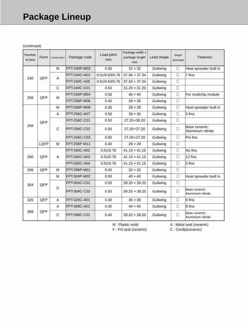
Package Lineup
72
(continued)
Number
of pinsForm Construction Package code
Lead pitchmm
Package width x
package length
mm
Lead shapeWeight
g/packageFeatures
240 QFP
M FPT-240P-M03 0.50 32 × 32 Gullwing Heat spreader built in
AFPT-240C-A03 0.51/0.63/0.76 37.34 × 37.34 Gullwing 7 fins
FPT-240C-A05 0.51/0.63/0.76 37.34 × 37.34 Gullwing C FPT-240C-C01 0.50 31.20 × 31.20 Gullwing
256 QFP MFPT-256P-M04 0.50 40 × 40 Gullwing For multichip module
FPT-256P-M06 0.40 28 × 28 Gullwing
256QFP
M FPT-256P-M09 0.40 28 × 28 Gullwing Heat spreader built in
A FPT-256C-A07 0.50 36 × 36 Gullwing 3 fins
C
FPT-256C-C01 0.50 27.20×39.20 Gullwing
FPT-256C-C02 0.50 27.20×27.20 Gullwing Base ceramic: Aluminium nitride
FPT-256C-C03 0.50 27.20×27.20 Gullwing Pin fins
LQFP M FPT-256P-M11 0.40 28 × 28 Gullwing
260 QFP A
FPT-260C-A02 0.51/0.76 41.15 × 41.15 Gullwing No fins
FPT-260C-A03 0.51/0.76 41.15 × 41.15 Gullwing 12 fins
FPT-260C-A04 0.51/0.76 41.15 × 41.15 Gullwing 5 fins
296 QFP M FPT-296P-M01 0.40 32 × 32 Gullwing
304 QFP
M FPT-304P-M02 0.50 40 × 40 Gullwing Heat spreader built in
C
FPT-304C-C01 0.50 39.20 × 39.20 Gullwing
FPT-304C-C02 0.50 39.20 × 39.20 Gullwing Base ceramic: Aluminium nitride
320 QFP A FPT-320C-A01 0.40 36 × 36 Gullwing 8 fins
368 QFPA FPT-368C-A01 0.40 40 × 40 Gullwing 8 fins
C FPT-368C-C01 0.40 39.20 × 39.20 Gullwing Base ceramic: Aluminium nitride
M : Plastic mold A : Metal seal (ceramic)F : Frit seal (ceramic) C : Cerdip(ceramic)

Package Lineup
73
Ceramic QFNs (LCCs)
Plastic and Ceramic QFJs
Plastic and Ceramic SOJs
Number
of pinsConstruction Package code
Lead pitchmm/mil
Package width × package lengthmm/mil
Features
16 F LCC-16C-F01 1.27/50 6.35 × 6.35/250 × 250 Body thickness: 100mil
32A
LCC-32C-A01 1.27/50 11.45 × 13.97/450 × 550 Body thickness: 130mil
LCC-32C-A06 1.016/40 10.67 × 10.67/420 × 420 Body thickness: 130mil
F LCC-32C-F01 1.27/50 11.45 × 13.97/450 × 450 Body thickness: 130mil
36 F LCC-36C-F01 1.27/50 13.97 × 13.97/550 × 550 Body thickness: 130mil
44 F LCC-44C-F01 1.27/50 16.51 × 16.51/650 × 650 Body thickness: 130mil
48 A LCC-48C-A01 1.016/40 14.22 × 14.22/560 × 560 Body thickness: 100mil
64 A LCC-64C-A01 1.016/40 18.29 × 18.29/720 × 720 Body thickness: 100mil
Number
of pinsConstruction Package code
Lead pitchmm/mil
Package width × package lengthmm/mil
Weight
g/packageFeatures
28 M LCC-28P-M03 1.27/50 453 × 453 1.00
32M LCC-32P-M02 1.27/50 450 × 550 0.96
C QFJ-32C-C01 1.27/50 450 × 550
44M LCC-44P-M02 1.27/50 653 × 653 2.05
C QFJ-44C-C01 1.27/50 650 × 650 68 M LCC-68P-M02 1.27/50 953 × 953 4.25
84 M LCC-84P-M02 1.27/50 1153 × 1153 6.20
M : Plastic mold A : Metal seal (ceramic)F : Frit seal (ceramic) C : Cerdip(ceramic)P : Resin seal
Number
of pinsConstruction Package code
Lead pitchmm/mil
Package widthmm/mil
Weight
g/packageFeatures
26 A LCC-26C-A01 1.27/50 8.03/316
28 A LCC-28C-A04 1.27/50 10.98/432 42 M LCC-42P-M01 1.27/50 10.16/400

Package Lineup
74
Plastic BGAs
Number
of pinsConstruction Package code
Lead pitchmm/mil
Pin matrix Features
48 MBGA-48P-M06 1.0 8 × 6
BGA-48P-M10 1.0 6 × 8
256 MBGA-256P-M01 1.27/50 20
BGA-256P-M02 1.27/50 20
352 M
BGA-352P-M01 1.27/50 26
BGA-352P-M02 1.27/50 26
BGA-352P-M03 1.27/50 26
BGA-352P-M04 1.27 26
BGA-352P-M05 1.27 26
BGA-352P-M08 416 M BGA-416P-M02 1.27/50 30
420 M
BGA-420P-M01 1.27/50 26
BGA-420P-M02 1.27/50 26
BGA-420P-M03 1.27 26
560 M BGA-560P-M01 576 M BGA-576P-M01 1.27 30
672 M BGA-672P-M01 1.27 34
720 M BGA-720P-M01 1196 M BGA-1196C-M01 1344 M BGA-1344C-M01 1600 M BGA-1600C-M01

Package Lineup
75
Plastic and Ceramic F-BGAs
Number
of pinsConstruction Package code
Lead pitchmm
Pin matrix Features
48 M
BGA-48P-M11 0.80 6 × 8
BGA-48P-M12 0.80 6 × 9
BGA-48P-M13 0.80 8 × 9
57 M BGA-57P-M01
61 M BGA-61P-M02
69 M BGA-69P-M02
77 M BGA-77P-M01
112 M BGA-112P-M01 0.80 11 × 11 (4 row)
120 M BGA-120P-M01 0.80 13 × 13 (3 row)
144 MBGA-144P-M01 0.80 14 × 14 (a part is 4 row)
BGA-144P-M02 0.80 13 × 13 (4 row)
168 M BGA-168P-M01 0.80 14 × 14 (a part is 5 row)
176 M BGA-176P-M02 0.80 14 × 14 (5 row)
192 MBGA-192P-M01 0.80 16 × 16 (4 row)
BGA-192P-M02 0.50 19 × 19 (3 row)
224 M BGA-224P-M03 0.80 18 × 18 (4 row)
240 M BGA-240P-M01 0.50 19 × 19 (4 row)
272 M BGA-272P-M02 0.80 21 × 21 (4 row)
288 M BGA-288P-M02 0.75 22 × 22 (4 row)
320 M BGA-320P-M01 0.80 21 × 21 (5 row)

Package Lineup
76
T-BGA Plastic
LGA Plastic
TCP Plastic
Number
of pinsConstruction Package code
Lead pitchmm/mil
Pin matrix Features
256 M BGA-256P-M04 1.27/50 20 Body thickness: 50mil
272 M BGA-272P-M01 1.27/50 21 Body thickness: 50mil
Number
of pinsConstruction Package code
Land pitchmm
Land matrix Features
48 MLGA-48P-M01 1.00 6 × 8
LGA-48P-M02 1.00 6 × 8
Number
of pinsForm Construction Package code
Lead pitchmm
Lead pitchmm/mil
Package width x package length
mm/milFeatures
44 DTP M DTP-44A-M01 0.80 1.27/50 10.16 × 18.41
160 QTP M QTP-160A-M01 0.30 1.27/50 14.00 × 14.00
208 QTP M QTP-208E-M01 0.30 1.27/50 20.00 × 20.00
256 QTP M QTP-256E-M01 0.30 1.27/50 24.00 × 24.00
400 QTP M QTP-400F-M01 0.30 1.27/50 28.00 × 28.00

Package Lineup
77
3.2.3 SMD Module
SIMM (SIPs, socket-mounted type)
MZIP
Number
of pinsConstruction Package code
Lead pitchmm/mil
Features
72 M
MSS-72P-P11 1.27/50 With 8 SOJs and 4 PLCCs mounted; module thickness: 200milmax.
MSS-72P-P12 1.27/50
MSS-72P-P23 1.27/50 With 8 SOJs and 4 PLCCs mounted; module thickness: 200milmax.
MSS-72P-P24 1.27/50 With 16 SOJs and 8 PLCCs mounted; module thickness: 350milmax.
MSS-72P-P27 1.27/50 With 16 SOJs mounted; module thickness: 350mil max.
MSS-72P-P29 1.27/50 With 8 SOJs mounted; module thickness: 200mil max.
MSS-72P-P39 1.27/50 With 16 SOJs mounted; module thickness: 350mil max.
MSS-72P-P43 1.27/50 With 8 TSOPs mounted; module thickness: 160mil max.
MSS-72P-P48 1.27/50 With 8 SOJs mounted; module thickness: 200mil max.
MSS-72P-P49 1.27/50 With 16 SOJs mounted; module thickness: 350mil max.
MSS-72P-P62 1.27/50 With 3 SOJs mounted; module thickness: 200mil max.
MSS-72P-P74 1.27/50 With 8 TSOPs mounted; module thickness: 160mil max.
MSS-72P-P75 1.27/50 With 9 SOJs mounted; module thickness: 160mil max.
MSS-72P-P76 1.27/50 With 18 SOJs mounted; module thickness: 350mil max.
MSS-72P-P77 1.27/50 With 8 SOJs mounted; module thickness: 200mil max.
MSS-72P-P78 1.27/50 With 16 SOJs mounted; module thickness: 350mil max.
MSS-72P-P79 1.27/50 With 8 SOJs mounted; module thickness: 200mil max.
MSS-72P-P80 1.27/50 With 16 SOJs mounted; module thickness: 350mil max.
MSS-72P-P81 1.27/50 With 12 SOJs mounted; module thickness: 350mil max.
MSS-72P-P82 1.27/50 With 12 SOJs mounted; module thickness: 350mil max.
MSS-72P-P84 1.27/50 With 18 TSOPs + 2 logic mounted; module thickness: 160milmax.
MSS-72P-P85 1.27/50 With 4 SOJs mounted; module thickness: 350mil max.
MSS-72P-P86 1.27/50 With 2 SOJs mounted; module thickness: 200mil max.
MSS-72P-P87 1.27/50
Number
of pinsConstruction Package code
Lead pitchmm/mil
Features
72 M MZP-72P-P01 1.27/50 With 20 SOJs mounted; module thickness: 350mil max.

Package Lineup
78
DIMM
(continued)
Number
of pinsConstruction Package code
Lead pitchmm/mil
Features
144 M
MDS-144P-P01 1.00/39 4 TSOPs + 1 logic mounted; module thickness: 150mil max.
MDS-144P-P02 1.00/39 8 TSOPs + 1 logic mounted; module thickness: 150mil max.
MDS-144P-P03 1.00/39 4 TSOPs + 1 logic mounted; module thickness: 150mil max.
MDS-144P-P04 1.00/39 8 TSOPs + 1 logic mounted; module thickness: 150mil max.
MDS-144P-P05 1.00/39 16 TSOPs + 1 logic mounted; module thickness: 150mil max.
MDS-144P-P06 1.00/39 4 TSOPs + 1 logic mounted; module thickness: 150mil max.
MDS-144P-P07 1.00/39 8 TSOPs + 1 logic mounted; module thickness: 150mil max.
MDS-144P-P08 0.80
MDS-144P-P09 0.80
MDS-144P-P12 0.80
168 M
MDS-168P-P04 1.27/50 18 TSOPs + 3 logic mounted; module thickness:157mil max.
MDS-168P-P05 1.27/50 16 TSOPs + 3 logic mounted; module thickness:157mil max.
MDS-168P-P06 1.27/50 8 SOPs + 3 logic mounted; module thickness:350mil max.
MDS-168P-P07 1.27/50 8 TSOPs + 1 logic mounted; module thickness:157mil max.
MDS-168P-P08 1.27/50 4 TSOPs + 1 logic mounted; module thickness:110mil max.
MDS-168P-P09 1.27/50 16 TSOPs + 1 logic mounted; module thickness:157mil max.
MDS-168P-P10 1.27/50 8 SOJs + 1 logic mounted; module thickness:200mil max.
MDS-168P-P11 1.27/50 16 SOJs + 1 logic mounted; module thickness:350mil max.
MDS-168P-P12 1.27/50 4 SOJs + 1 logic mounted; module thickness:200mil max.
MDS-168P-P13 1.27/50 8 TSOPs + 1 logic mounted; module thickness:157mil max.
MDS-168P-P14 1.27/50 16 TSOPs + 1 logic mounted; module thickness:157mil max.
MDS-168P-P16 1.27
MDS-168P-P17 1.27
MDS-168P-P18 1.27
MDS-168P-P19 1.27
MDS-168P-P20 1.27
MDS-168P-P21 1.27
MDS-168P-P22 1.27
MDS-168P-P23 1.27
MDS-168P-P24 1.27
MDS-168P-P25 1.27
M : Plastic mold
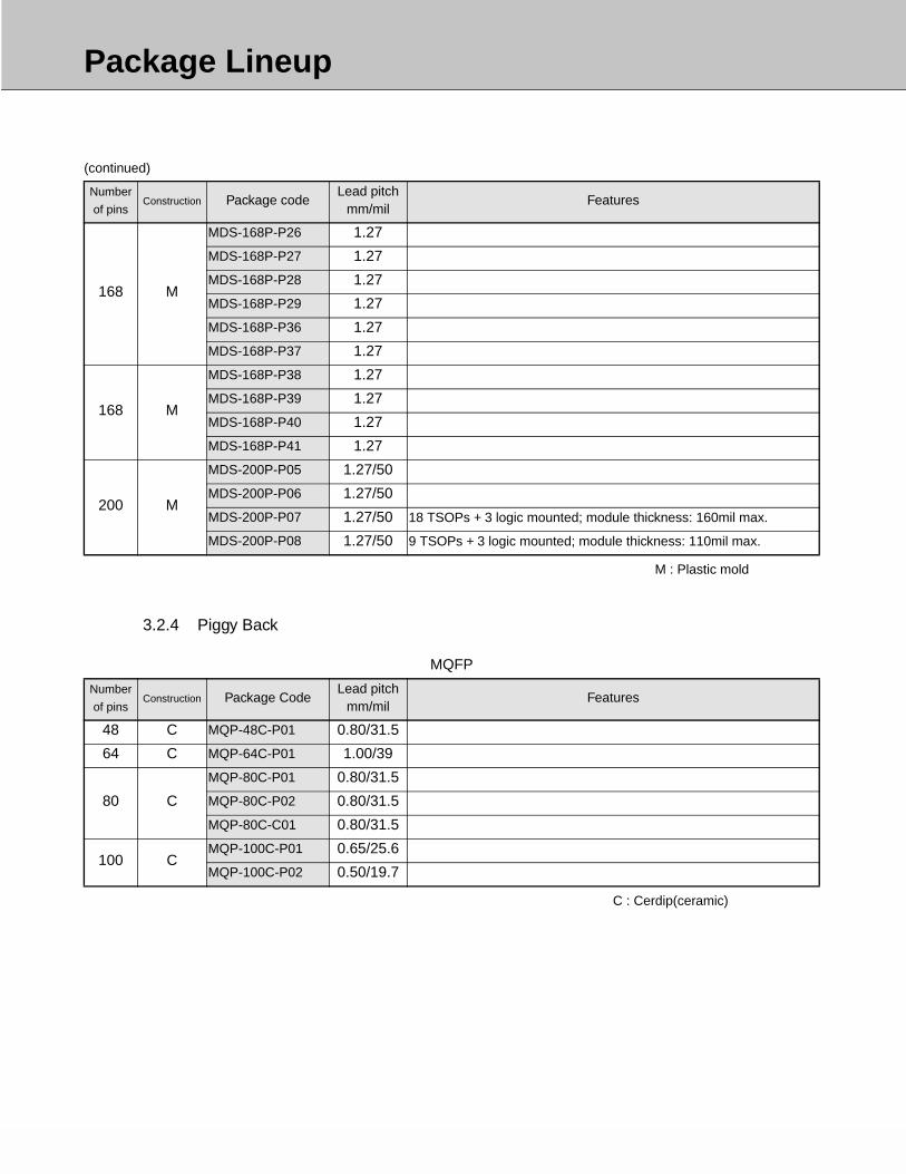
Package Lineup
79
(continued)
3.2.4 Piggy Back
MQFP
Number
of pinsConstruction Package code
Lead pitchmm/mil
Features
168 M
MDS-168P-P26 1.27
MDS-168P-P27 1.27
MDS-168P-P28 1.27
MDS-168P-P29 1.27
MDS-168P-P36 1.27
MDS-168P-P37 1.27
168 M
MDS-168P-P38 1.27
MDS-168P-P39 1.27
MDS-168P-P40 1.27
MDS-168P-P41 1.27
200 M
MDS-200P-P05 1.27/50
MDS-200P-P06 1.27/50
MDS-200P-P07 1.27/50 18 TSOPs + 3 logic mounted; module thickness: 160mil max.
MDS-200P-P08 1.27/50 9 TSOPs + 3 logic mounted; module thickness: 110mil max.
M : Plastic mold
Number
of pinsConstruction Package Code
Lead pitchmm/mil
Features
48 C MQP-48C-P01 0.80/31.5
64 C MQP-64C-P01 1.00/39
80 C
MQP-80C-P01 0.80/31.5
MQP-80C-P02 0.80/31.5
MQP-80C-C01 0.80/31.5
100 CMQP-100C-P01 0.65/25.6
MQP-100C-P02 0.50/19.7
C : Cerdip(ceramic)
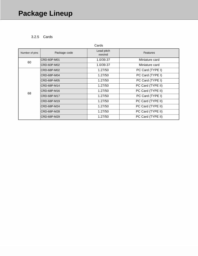
Package Lineup
80
3.2.5 Cards
Cards
Number of pins Package codeLead pitch
mm/milFeatures
60CRD-60P-M01 1.0/39.37 Miniature card
CRD-60P-M02 1.0/39.37 Miniature card
68
CRD-68P-M02 1.27/50 PC Card (TYPE I)
CRD-68P-M04 1.27/50 PC Card (TYPE I)
CRD-68P-M05 1.27/50 PC Card (TYPE I)
CRD-68P-M14 1.27/50 PC Card (TYPE II)
CRD-68P-M16 1.27/50 PC Card (TYPE II)
CRD-68P-M17 1.27/50 PC Card (TYPE I)
CRD-68P-M19 1.27/50 PC Card (TYPE II)
CRD-68P-M24 1.27/50 PC Card (TYPE II)
CRD-68P-M28 1.27/50 PC Card (TYPE II)
CRD-68P-M29 1.27/50 PC Card (TYPE II)
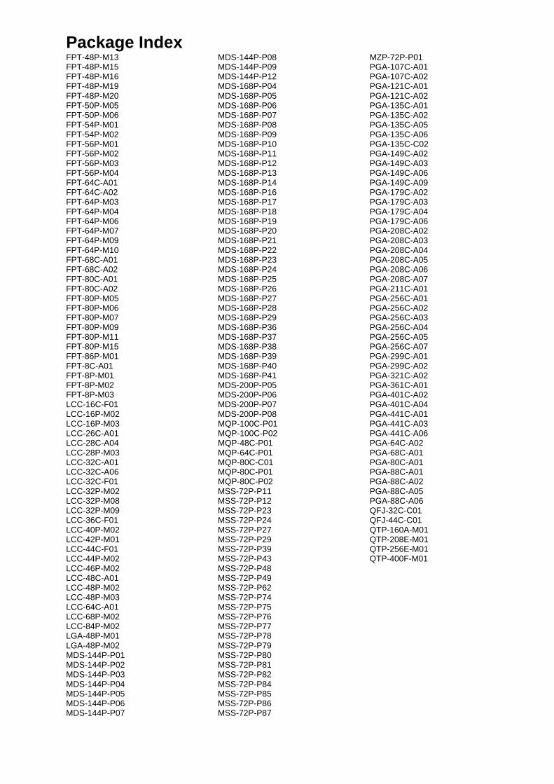
Package IndexFPT-48P-M13FPT-48P-M15FPT-48P-M16FPT-48P-M19FPT-48P-M20FPT-50P-M05FPT-50P-M06FPT-54P-M01FPT-54P-M02FPT-56P-M01FPT-56P-M02FPT-56P-M03FPT-56P-M04FPT-64C-A01FPT-64C-A02FPT-64P-M03FPT-64P-M04FPT-64P-M06FPT-64P-M07FPT-64P-M09FPT-64P-M10FPT-68C-A01FPT-68C-A02FPT-80C-A01FPT-80C-A02FPT-80P-M05FPT-80P-M06FPT-80P-M07FPT-80P-M09FPT-80P-M11FPT-80P-M15FPT-86P-M01FPT-8C-A01FPT-8P-M01FPT-8P-M02FPT-8P-M03LCC-16C-F01LCC-16P-M02LCC-16P-M03LCC-26C-A01LCC-28C-A04LCC-28P-M03LCC-32C-A01LCC-32C-A06LCC-32C-F01LCC-32P-M02LCC-32P-M08LCC-32P-M09LCC-36C-F01LCC-40P-M02LCC-42P-M01LCC-44C-F01LCC-44P-M02LCC-46P-M02LCC-48C-A01LCC-48P-M02LCC-48P-M03LCC-64C-A01LCC-68P-M02LCC-84P-M02LGA-48P-M01LGA-48P-M02MDS-144P-P01MDS-144P-P02MDS-144P-P03MDS-144P-P04MDS-144P-P05MDS-144P-P06MDS-144P-P07
MDS-144P-P08MDS-144P-P09MDS-144P-P12MDS-168P-P04MDS-168P-P05MDS-168P-P06MDS-168P-P07MDS-168P-P08MDS-168P-P09MDS-168P-P10MDS-168P-P11MDS-168P-P12MDS-168P-P13MDS-168P-P14MDS-168P-P16MDS-168P-P17MDS-168P-P18MDS-168P-P19MDS-168P-P20MDS-168P-P21MDS-168P-P22MDS-168P-P23MDS-168P-P24MDS-168P-P25MDS-168P-P26MDS-168P-P27MDS-168P-P28MDS-168P-P29MDS-168P-P36MDS-168P-P37MDS-168P-P38MDS-168P-P39MDS-168P-P40MDS-168P-P41MDS-200P-P05MDS-200P-P06MDS-200P-P07MDS-200P-P08MQP-100C-P01MQP-100C-P02MQP-48C-P01MQP-64C-P01MQP-80C-C01MQP-80C-P01MQP-80C-P02MSS-72P-P11MSS-72P-P12MSS-72P-P23MSS-72P-P24MSS-72P-P27MSS-72P-P29MSS-72P-P39MSS-72P-P43MSS-72P-P48MSS-72P-P49MSS-72P-P62MSS-72P-P74MSS-72P-P75MSS-72P-P76MSS-72P-P77MSS-72P-P78MSS-72P-P79MSS-72P-P80MSS-72P-P81MSS-72P-P82MSS-72P-P84MSS-72P-P85MSS-72P-P86MSS-72P-P87
MZP-72P-P01PGA-107C-A01PGA-107C-A02PGA-121C-A01PGA-121C-A02PGA-135C-A01PGA-135C-A02PGA-135C-A05PGA-135C-A06PGA-135C-C02PGA-149C-A02PGA-149C-A03PGA-149C-A06PGA-149C-A09PGA-179C-A02PGA-179C-A03PGA-179C-A04PGA-179C-A06PGA-208C-A02PGA-208C-A03PGA-208C-A04PGA-208C-A05PGA-208C-A06PGA-208C-A07PGA-211C-A01PGA-256C-A01PGA-256C-A02PGA-256C-A03PGA-256C-A04PGA-256C-A05PGA-256C-A07PGA-299C-A01PGA-299C-A02PGA-321C-A02PGA-361C-A01PGA-401C-A02PGA-401C-A04PGA-441C-A01PGA-441C-A03PGA-441C-A06PGA-64C-A02PGA-68C-A01PGA-80C-A01PGA-88C-A01PGA-88C-A02PGA-88C-A05PGA-88C-A06QFJ-32C-C01QFJ-44C-C01QTP-160A-M01QTP-208E-M01QTP-256E-M01QTP-400F-M01

QFJ
Plastic
Ceramic
SOJ
Plastic
Ceramic
BGA
Plastic
T-BGA
Plastic
TCP
Plastic
SMD MODULE
SIMM
MZIP
DIMM
PIGGY BACK
MQFP
CARD
MINIATURE CARD
PC CARD
DRAM CARD
Package Outline Diagrams4DIP (Standard DIP, SH-DIP, SK-DIP, SL-DIP)
Plastic
Ceramic
SIP
Plastic
ZIP (Standard ZIP, SZIP)
Plastic
PGA
Plastic
Ceramic
SOP (SOP, SOL, SSOP, TSOP)
Plastic
Ceramic
SON
Plastic
BCC
Plastic
QFP (QFP, LQFP, TQFP, TPQ)
Plastic
Ceramic
QFN (LCC)
Ceramic
PCLP
Plastic

Sockets
1
5.1 Sockets
The sockets listed in section 5.2, “List of test sockets,” are available as test sockets. For details, on functions,performance, price and delivery, contact the respective socket manufacturers directly. Fujitsu also has its ownsockets under development. If a socket not listed in the charts is required, contact the sales department indi-cated on the endpaper of this data book.
Contact information
*1: Fuso Trading is the Japanese agent for Wells Co. of the U.S.*2: Showa Densen Trading is a representative for Texas Instruments, Japan.*3: Macnica is an agent for Sumitomo 3M.
Company Address of headquarters Telephone Name
Yamaichi Electric Mfg. Co.,Ltd.
3-28-7, Nakamagome, Ota-ku, Tokyo,143
+81-3-3778-6102 Mr. Oguchi
Enplas Corp.Kojima Bldg 9th Floor, 2-15-1, Dote-machi,Ohmiya-shi, Saitama, 330
+81-48-643-7676 Mr. Watanabe
Fuso Trading *1 TBR Bldg, 2-10-2, Nagatacho, Chiyoda-ku,Tokyo, 100
+81-3-3581-9056 Mr. Itoo
Showa Densen Trading *2Tomozuna Bldg, 2-17-22, Mita, Minato-ku,Tokyo, 108
+81-3-5440-4710 Mr. Kuroda
UnitechnoMaekawa Shibaura Bldg2, 2-13-9, Shiba-ura,Minato-ku, Tokyo, 108
+81-3-5476-5661 Mr. Yamazaki
Macnica *3Shirayama Hi-tech Park1-22-2,Shirayama, Midori-ku, Yokohama, 226
-81-45-939-6116 Mr. Suzuki

Sockets
2
5.2 List of Test Sockets
Plastic SOPs
(continued)
Package Socket
Number of pins
Package code Model number Manufacturer
8FPT-8P-M01
IC51-902-2.KS-8571 Yamaichi Electric Mfg.
FP-16 (20M) -1.27-06A Enplas
FPT-8P-M02 FP-8 (16H) -1.27-06 Enplas
14
FPT-14P-M03IC51-0162-658 Yamaichi Electric Mfg.
FP-14 (16H) -1.27-05 Enplas
FPT-14P-M04IC51-902-2.KS-8571 Yamaichi Electric Mfg.
FP-14 (20) -1.27-06 Enplas
16
FPT-16P-M03IC51-347.KS-5755 Yamaichi Electric Mfg.
FP-16 (28Z) -1.27-10 Enplas
FPT-16P-M04IC51-0162-658 Yamaichi Electric Mfg.
FP-16-1.27-05 Enplas
FPT-16P-M05IC51-0162-911 Yamaichi Electric Mfg.
FP-16-0.65-01A Enplas
FPT-16P-M06IC51-902-2.KS-8571 Yamaichi Electric Mfg.
FP-16 (20) -1.27-06 Enplas
20
FPT-20P-M01IC51-793.KS-7536 Yamaichi Electric Mfg.
FP-20-1.27-06 Enplas
FPT-20P-M02IC51-0202-347-2 Yamaichi Electric Mfg.
FP-20-1.27-03 Enplas
FPT-20P-M03IC51-0202-912 Yamaichi Electric Mfg.
FP-20-0.65-01A Enplas
FPT-20P-M04IC51-0202-912 Yamaichi Electric Mfg.
FP-20-0.65-01A Enplas
FPT-20P-M05IC51-0202-347-2 Yamaichi Electric Mfg.
FP-20-1.27-03 Enplas
24
FPT-24P-M01 IC51-0242-793 Yamaichi Electric Mfg.
FPT-24P-M02IC51-371.KS-7842 Yamaichi Electric Mfg.
FP-24 (28S) -1.27-08 Enplas
FPT-24P-M03IC51-0242-913 Yamaichi Electric Mfg.
FP-24-0.65-01A Enplas
28
FPT-28P-M01IC51-0302-904 Yamaichi Electric Mfg.
FP-28-1.27-10 Enplas
FPT-28P-M17IC51-474.KS-94455 Yamaichi Electric Mfg.
FP-28-1.27-22 Enplas

Sockets
3
(continued)
(continued)
Package Socket
Number of pins
Package code Model number Manufacturer
30 FPT-30P-M02IC51-0302-914 Yamaichi Electric Mfg.
FP-30-0.65-01A Enplas
32
FPT-32P-M02IC51-0322-937 Yamaichi Electric Mfg.
OTS-32-1.27-06 Enplas
FPT-32P-M03IC51-0322-667-2 Yamaichi Electric Mfg.
OTS-32-1.27-12 Enplas
32
FPT-32P-M24
IC51-0322-1207 Yamaichi Electric Mfg.
OTS-32-0.5-02 Enplas
648-0322211-A41 Wells (Fuso Trading)
FPT-32P-M25
IC51-0322-1207 Yamaichi Electric Mfg.
OTS-32-0.5-02 Enplas
648-0322211-A41 Wells (Fuso Trading)
34FPT-34P-M01 IC51-0342-741 Yamaichi Electric Mfg.
FPT-34P-M02 IC51-0342-741 Yamaichi Electric Mfg.
40
FPT-40P-M01 IC51-0402-708 Yamaichi Electric Mfg.
FPT-40P-M04 IC51-0402-708 Yamaichi Electric Mfg.
FPT-40P-M05 IC51-0402-708 Yamaichi Electric Mfg.
FPT-40P-M06IC51-0402-1174 Yamaichi Electric Mfg.
648-0402211-A41 Wells (Fuso Trading)
FPT-40P-M07IC51-0402-1174 Yamaichi Electric Mfg.
648-0402211-A41 Wells (Fuso Trading)
44
FPT-44P-M07
IC235-0402-005 Yamaichi Electric Mfg.
FP-40 (44) -0.8-03 Enplas
674C1444011FA11 Wells (Fuso Trading)
FPT-44P-M08
IC235-0402-005 Yamaichi Electric Mfg.
FP-40 (44) -0.8-03 Enplas
674C1444011FA11 Wells (Fuso Trading)
FPT-44P-M16 IC51-0442-1315 Yamaichi Electric Mfg.
FPT-44P-M18IC297-0442-003P Yamaichi Electric Mfg.
674C1442211FA13 Wells (Fuso Trading)
48
FPT-48P-M19IC189-0482-077P Yamaichi Electric Mfg.
648-0482211-A41 Wells (Fuso Trading)
FPT-48P-M20IC189-0482-077P Yamaichi Electric Mfg.
648-0482211-A41 Wells (Fuso Trading)
50FPT-50P-M05 674C1502211FA11 Wells (Fuso Trading)
FPT-50P-M06 674C1504411FA11 Wells (Fuso Trading)

Sockets
4
(continued)
Ceramic SOPs
Plastic QFPs
(continued)
Package Socket
Number of pins
Package code Model number Manufacturer
54
FPT-54P-M01 IC235-0542-218P-2 Yamaichi Electric Mfg.
FPT-54P-M02IC297-0542-004P Yamaichi Electric Mfg.
674C1542211FA13 Wells (Fuso Trading)
56
FPT-56P-M01 IC354-0562-010P Yamaichi Electric Mfg.
FPT-56P-M02 IC354-0562-010P Yamaichi Electric Mfg.
FPT-56P-M03 CSP056-070 Japan TI (Showa Densen Trading)
FPT-56P-M04 TS4-056040-019 Unitechno
86 FPT-86P-M01IC297-0862-005P Yamaichi Electric Mfg.
674C2862211-A11 Wells (Fuso Trading)
Package Socket
Number of pins
Package code Model number Manufacturer
8 FPT-8C-A01 IC51-793.KS-8194 Yamaichi Electric Mfg.
16 FPT-16C-C02 IC51-902.KS-8571 Yamaichi Electric Mfg.
Package Socket
Number of pins
Package code Model number Manufacturer
32 FPT-32P-M21 FPQ-32-0.8-01 Enplas
44 FPT-44P-M11IC51-0444-228 Yamaichi Electric Mfg.
FPQ-44-0.8-14A Enplas
48
FPT-48P-M05IC51-0484-806 Yamaichi Electric Mfg.
FPQ-48-0.5-06 Enplas
FPT-48P-M13 FPQ-48-0.8-01 Enplas
FPT-14P-M15 FPQ-48-0.8-05 Enplas
FPT-48P-M16IC51-0484-630 Yamaichi Electric Mfg.
FPQ-48-0.8-05 Enplas
64
FPT-64P-M03
QP1-064050-108 Unitechno
IC51-0644-807 Yamaichi Electric Mfg.
FPQ-64-0.5-01 Enplas
FPT-64P-M04
QP1-064050-108 Unitechno
IC51-0644-807 Yamaichi Electric Mfg.
FPQ-64-0.5-01 Enplas

Sockets
5
(continued)
(continued)
Package Socket
Number of pins
Package code Model number Manufacturer
64
FPT-64P-M06
680H642111 Wells (Fuso Trading)
IC53-108.KS-7507 Yamaichi Electric Mfg.
FPQ-64-1.0-08A Enplas
FPT-64P-M07IC53-108.KS-7507 Yamaichi Electric Mfg.
FPQ-64-1.0-08A Enplas
FPT-64P-M09IC51-0644-1602 Yamaichi Electric Mfg.
FPQ-64-0.65-02 Enplas
FPT-64P-M10
680H642111 Wells (Fuso Trading)
IC53-108.KS-7507 Yamaichi Electric Mfg.
FPQ-64-1.0-08A Enplas
80
FPT-80P-M05
IC234-0804-026P Yamaichi Electric Mfg.
IC51-0804-808 Yamaichi Electric Mfg.
OTQ-80-0.5-02 Enplas
QP1-080050-147 Unitechno
FPQ-80-0.5-04 Enplas
FPT-80P-M06
IC201-0804-005 Yamaichi Electric Mfg.
IC51-0804-819-4 Yamaichi Electric Mfg.
FPQ-80-0.8-13A Enplas
QP1-080080-007 Unitechno
80
FPT-80P-M07
IC51-0804-819-4 Yamaichi Electric Mfg.
FPQ-80-0.8-13A Enplas
QP1-080080-007 Unitechno
FPT-80P-M11
IC218-0804-007P Yamaichi Electric Mfg.
IC51-1311.KS-12951 Enplas
FPQ-80-0.65-09A Unitechno
FPT-80P-M15QP1-080050-147 Unitechno
IC234-0804-026P Yamaichi Electric Mfg.
100
FPT-100P-M05
IC234-1004-023P Yamaichi Electric Mfg.
IC51-1004-809 Yamaichi Electric Mfg.
FPQ-100-0.5-10A Enplas
QP1-100050-146 Unitechno
FPT-100P-M06
IC234-1004-009P Yamaichi Electric Mfg.
IC51-1004-814-4 Yamaichi Electric Mfg.
FPQ-100-0.65-11A Enplas
QP1-100065-004 Unitechno

Sockets
6
(continued)
(continued)
Package Socket
Number of pins
Package code Model number Manufacturer
100
FPT-100P-M07
IC51-1004-814-4 Yamaichi Electric Mfg.
FPQ-100-0.65-11A Enplas
QP1-100065-004 Unitechno
FPT-100P-M09
IC51-1004-809 Yamaichi Electric Mfg.
FPQ-100-0.5-10A Enplas
QP1-100050-146 Unitechno
FPT-100P-M18 IC234-045P.AC-10654 Yamaichi Electric Mfg.
FPT-100P-M19
680-1001111-002 Wells (Fuso Trading)
CQF100-151 Japan TI (Showa Densen Trading)
QP1-100065-003 Unitechno
IC51-1004-814-7 Yamaichi Electric Mfg.
120
FPT-120P-M03
IC234-1204-065P Yamaichi Electric Mfg.
IC51-844.KS-7692 Yamaichi Electric Mfg.
FPQ-120-0.8-03A Enplas
QP1-120080-177 Unitechno
FPT-120P-M04
IC234-1204-065P Yamaichi Electric Mfg.
IC51-844.KS-7692 Yamaichi Electric Mfg.
FPQ-120-0.8-03A Enplas
QP1-120080-177 Unitechno
FPT-120P-M13 QP1-144050-044-1 Unitechno
FPT-120P-M21IC234-1204-058P Yamaichi Electric Mfg.
QP1-120050-272 Unitechno
144
FPT-144P-M01
IC51-1444-1014 Yamaichi Electric Mfg.
FPQ-144-0.65-02A Enplas
QP1-144065-178 Unitechno
FPT-144P-M02
IC51-1444-1014 Yamaichi Electric Mfg.
FPQ-144-0.65-02A Enplas
QP1-144065-178 Unitechno
FPT-144P-M03 QP1-1440050-044 Unitechno
FPT-144P-M08IC51-1444-1354-7 Yamaichi Electric Mfg.
FPQ-144-0.5-03 Enplas
FPT-144P-M12 IC234-1444-053P Yamaichi Electric Mfg.

Sockets
7
(continued)
Package Socket
Number of pins
Package code Model number Manufacturer
160
FPT-160P-M03
IC234-1604-064P Yamaichi Electric Mfg.
IC51-845.KS-7764 Yamaichi Electric Mfg.
FPQ-160-0.65-06A Enplas
QP1-160065-165 Unitechno
FPT-160P-M04
IC234-1604-064P Yamaichi Electric Mfg.
IC51-845.KS-7764 Yamaichi Electric Mfg.
FPQ-160-0.65-06A Enplas
QP1-160065-165 Unitechno
FPT-160P-M11 QP1-160065-010 Unitechno
176 FPT-176P-M02 IC234-1764-002P Yamaichi Electric Mfg.
208
FPT-208P-M01
QP4-208050-024 Unitechno
IC51-2084-1052-9 Yamaichi Electric Mfg.
FPQ-208-0.5-06 Enplas
QP1-208050-014 Unitechno
FPT-208P-M04QP4-208050-024 Unitechno
QP1-208050-182 Unitechno
FPT-208P-M06 IC201-001.AC-08598 Yamaichi Electric Mfg.
216 FPT-216P-M01 IC234-2164-050P Yamaichi Electric Mfg.
240 FPT-240P-M03 EXC97072CQF240 Japan TI (Showa Densen Trading)
304 FPT-304P-M02 IC201-004.AC-07901 Yamaichi Electric Mfg.

Sockets
8
Ceramic QFPs
Package Socket
Number of pins
Package code Model number Manufacturer
16 FPT-16C-A01 FP-16-0.0-02 Enplas
48 FPT-48C-A01 FPQ-48-0.8-03 Enplas
64
FPT-64C-A01IC51-820-2.KS-9376 Yamaichi Electric Mfg.
OTQ-64-1.0-03 Enplas
FPT-64C-A02IC51-820-2.KS-9177 Yamaichi Electric Mfg.
OTQ-64-1.0-03 Enplas
80
FPT-80C-A01
IC51-0804-819-4 Yamaichi Electric Mfg.
FPQ-80-0.8-13A Enplas
QP1-080080-007 Unitechno
FPT-80C-A02FPQ-80-0.8-13A Enplas
QP1-080080-007 Unitechno
100
FPT-100C-A01
IC51-1004-814-4 Yamaichi Electric Mfg.
FPQ-100-0.65-10D Enplas
QP1-100065-004 Unitechno
FPT-100C-A02 FPQ-100-0.65-10D Enplas
FPT-100C-C01FPQ-100-0.5-10A Enplas
QP1-100050-146 Unitechno
120
FPT-120C-A01
IC51-844.KS-7692 Yamaichi Electric Mfg.
FPQ-120-0.8-03A Enplas
QP1-120080-177 Unitechno
FPT-120C-C01
IC51-844.KS-7692 Yamaichi Electric Mfg.
FPQ-120-0.8-03A Enplas
QP1-120080-177 Unitechno
144 FPT-144C-C01FPQ-144-0.65-02A Enplas
QP1-144065-178 Unitechno
160
FPT-160C-A01FPQ-160-0.65-06A Enplas
QP1-160065-165 Unitechno
FPT-160C-C01FPQ-160-0.65-06A Enplas
QP1-160065-165 Unitechno
FPT-160C-C02FPQ-160-0.65-06A Enplas
QP1-160065-165 Unitechno
FPT-160C-C04FPQ-160-0.65-06A Enplas
QP1-160065-165 Unitechno

Sockets
9
Ceramic LCCs
Plastic QFJs (PLCCs) , SOJs
Package Socket
Number of pins
Package code Model number Manufacturer
16 LCC-16C-F01 IC53-0164-083 Yamaichi Electric Mfg.
32
LCC-32C-A01IC51-0324-1259 Yamaichi Electric Mfg.
LCC-32-1.27- (03) Enplas
LCC-32C-A06 IC53-0324-098 Yamaichi Electric Mfg.
LCC-32C-F01IC53-0324-065 Yamaichi Electric Mfg.
LCC-32-1.27- (03) Enplas
36 LCC-36C-F01 IC53-0364-296 Yamaichi Electric Mfg.
44 LCC-44C-F01IC53-0444-306 Yamaichi Electric Mfg.
LCC-44-1.27- (01) Enplas
48 LCC-48C-A01 IC53-0484-100 Yamaichi Electric Mfg.
Package Socket
Number of pins
Package code Model number Manufacturer
28 LCC-28P-M03
IC51-0284-399 Yamaichi Electric Mfg.
PLCC-28-1.27-30 Enplas
647X1281912 Wells (Fuso Trading)
32 LCC-32P-M02
IC51-0324-453 Yamaichi Electric Mfg.
PLCC-32-1.27-30 Enplas
647X0321912 Wells (Fuso Trading)
42 LCC-42P-M01IC100-4204-G Yamaichi Electric Mfg.
IC255-4204 Yamaichi Electric Mfg.
44 LCC-44P-M02
IC51-0444-400 Yamaichi Electric Mfg.
PLCC-44-1.27-30 Enplas
647X1441912 Wells (Fuso Trading)
68 LCC-68P-M02
IC51-0684-390-2 Yamaichi Electric Mfg.
PLCC-68-1.27-30 Enplas
647X1681912 Wells (Fuso Trading)
84 LCC-84P-M02
IC51-0844-401-2 Yamaichi Electric Mfg.
PLCC-84-1.27-30 Enplas
647X1841912 Wells (Fuso Trading)
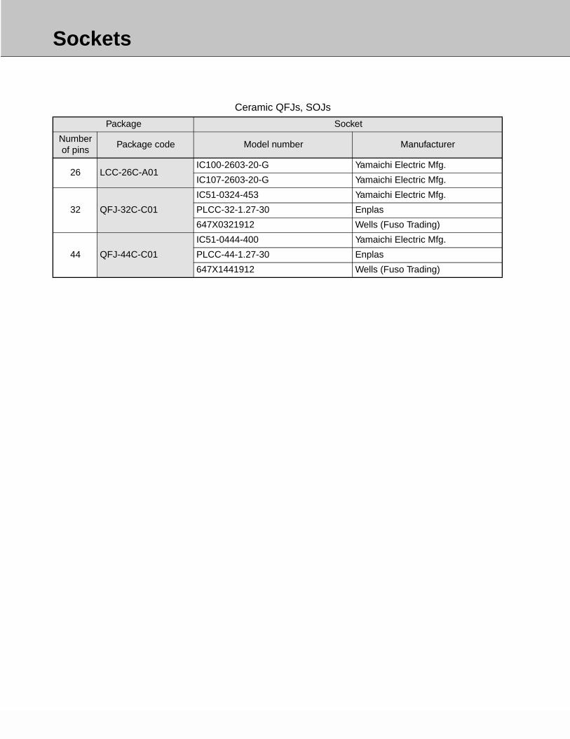
Sockets
10
Ceramic QFJs, SOJs
Package Socket
Number of pins
Package code Model number Manufacturer
26 LCC-26C-A01IC100-2603-20-G Yamaichi Electric Mfg.
IC107-2603-20-G Yamaichi Electric Mfg.
32 QFJ-32C-C01
IC51-0324-453 Yamaichi Electric Mfg.
PLCC-32-1.27-30 Enplas
647X0321912 Wells (Fuso Trading)
44 QFJ-44C-C01
IC51-0444-400 Yamaichi Electric Mfg.
PLCC-44-1.27-30 Enplas
647X1441912 Wells (Fuso Trading)

Sockets
11
Modules
(continued)
Package Socket
Number of pins
Package code Model number Manufacturer
MSS
MSS-30P-P03 IC-176-4 Yamaichi Electric Mfg.
MSS-30P-P04 IC-176-4 Yamaichi Electric Mfg.
MSS-30P-P11 IC-176-4 Yamaichi Electric Mfg.
MSS-30P-P12 IC-176-4 Yamaichi Electric Mfg.
MSS-72P-P11 IC-176-2 Yamaichi Electric Mfg.
MSS-72P-P12 IC-176-2 Yamaichi Electric Mfg.
MSS-72P-P16 IC-176-2 Yamaichi Electric Mfg.
MSS-72P-P17 IC-176-2 Yamaichi Electric Mfg.
MSS-72P-P18 IC-176-2 Yamaichi Electric Mfg.
MSS-72P-P19 IC-176-2 Yamaichi Electric Mfg.
MSS-72P-P23 IC-176-2 Yamaichi Electric Mfg.
MSS-72P-P24 IC-176-2 Yamaichi Electric Mfg.
MSS-72P-P27 IC-176-2 Yamaichi Electric Mfg.
MSS-72P-P29 IC-176-2 Yamaichi Electric Mfg.
MSS-72P-P39 IC-176-2 Yamaichi Electric Mfg.
MSS-72P-P43 IC-176-2 Yamaichi Electric Mfg.
MSS-72P-P44 IC-176-2 Yamaichi Electric Mfg.
MSS-72P-P48 IC-176-2 Yamaichi Electric Mfg.
MSS-72P-P49 IC-176-2 Yamaichi Electric Mfg.
MSS-72P-P62 IC-176-2 Yamaichi Electric Mfg.
MSS-72P-P70 IC-176-2 Yamaichi Electric Mfg.
MSS-72P-P74 IC-176-2 Yamaichi Electric Mfg.
MSS-72P-P75 IC-176-2 Yamaichi Electric Mfg.
MSS-72P-P76 IC-176-2 Yamaichi Electric Mfg.
MSS-72P-P77 IC-176-2 Yamaichi Electric Mfg.
MSS-72P-P78 IC-176-2 Yamaichi Electric Mfg.
MSS-72P-P79 IC-176-2 Yamaichi Electric Mfg.
MSS-72P-P80 IC-176-2 Yamaichi Electric Mfg.
MSS-72P-P81 IC-176-2 Yamaichi Electric Mfg.
MSS-72P-P82 IC-176-2 Yamaichi Electric Mfg.
MSS-72P-P84 IC-176-2 Yamaichi Electric Mfg.
MSS-72P-P85 IC-176-2 Yamaichi Electric Mfg.
MSS-72P-P86 IC-176-2 Yamaichi Electric Mfg.
MSS-72P-P87 IC-176-2 Yamaichi Electric Mfg.
MDSMDS-144P-P01 IC-497-1-2 Yamaichi Electric Mfg.
MDS-144P-P02 IC-497-1-2 Yamaichi Electric Mfg.
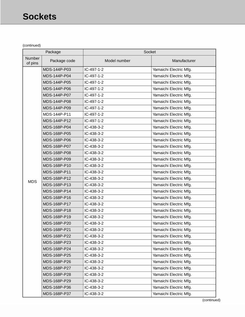
Sockets
12
(continued)
(continued)
Package Socket
Number of pins
Package code Model number Manufacturer
MDS
MDS-144P-P03 IC-497-1-2 Yamaichi Electric Mfg.
MDS-144P-P04 IC-497-1-2 Yamaichi Electric Mfg.
MDS-144P-P05 IC-497-1-2 Yamaichi Electric Mfg.
MDS-144P-P06 IC-497-1-2 Yamaichi Electric Mfg.
MDS-144P-P07 IC-497-1-2 Yamaichi Electric Mfg.
MDS-144P-P08 IC-497-1-2 Yamaichi Electric Mfg.
MDS-144P-P09 IC-497-1-2 Yamaichi Electric Mfg.
MDS-144P-P11 IC-497-1-2 Yamaichi Electric Mfg.
MDS-144P-P12 IC-497-1-2 Yamaichi Electric Mfg.
MDS-168P-P04 IC-438-3-2 Yamaichi Electric Mfg.
MDS-168P-P05 IC-438-3-2 Yamaichi Electric Mfg.
MDS-168P-P06 IC-438-3-2 Yamaichi Electric Mfg.
MDS-168P-P07 IC-438-3-2 Yamaichi Electric Mfg.
MDS-168P-P08 IC-438-3-2 Yamaichi Electric Mfg.
MDS-168P-P09 IC-438-3-2 Yamaichi Electric Mfg.
MDS-168P-P10 IC-438-3-2 Yamaichi Electric Mfg.
MDS-168P-P11 IC-438-3-2 Yamaichi Electric Mfg.
MDS-168P-P12 IC-438-3-2 Yamaichi Electric Mfg.
MDS-168P-P13 IC-438-3-2 Yamaichi Electric Mfg.
MDS-168P-P14 IC-438-3-2 Yamaichi Electric Mfg.
MDS-168P-P16 IC-438-3-2 Yamaichi Electric Mfg.
MDS-168P-P17 IC-438-3-2 Yamaichi Electric Mfg.
MDS-168P-P18 IC-438-3-2 Yamaichi Electric Mfg.
MDS-168P-P19 IC-438-3-2 Yamaichi Electric Mfg.
MDS-168P-P20 IC-438-3-2 Yamaichi Electric Mfg.
MDS-168P-P21 IC-438-3-2 Yamaichi Electric Mfg.
MDS-168P-P22 IC-438-3-2 Yamaichi Electric Mfg.
MDS-168P-P23 IC-438-3-2 Yamaichi Electric Mfg.
MDS-168P-P24 IC-438-3-2 Yamaichi Electric Mfg.
MDS-168P-P25 IC-438-3-2 Yamaichi Electric Mfg.
MDS-168P-P26 IC-438-3-2 Yamaichi Electric Mfg.
MDS-168P-P27 IC-438-3-2 Yamaichi Electric Mfg.
MDS-168P-P28 IC-438-3-2 Yamaichi Electric Mfg.
MDS-168P-P29 IC-438-3-2 Yamaichi Electric Mfg.
MDS-168P-P36 IC-438-3-2 Yamaichi Electric Mfg.
MDS-168P-P37 IC-438-3-2 Yamaichi Electric Mfg.
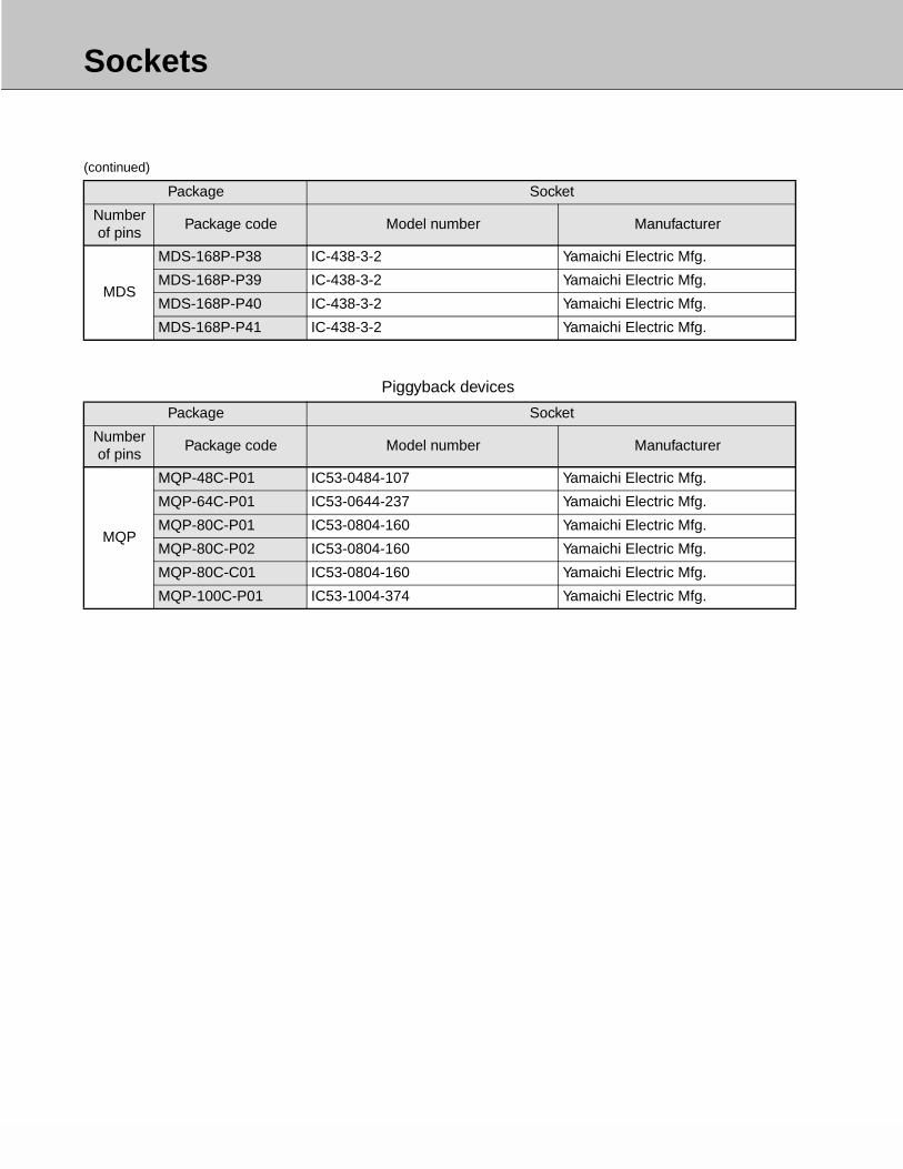
Sockets
13
(continued)
Piggyback devices
Package Socket
Number of pins
Package code Model number Manufacturer
MDS
MDS-168P-P38 IC-438-3-2 Yamaichi Electric Mfg.
MDS-168P-P39 IC-438-3-2 Yamaichi Electric Mfg.
MDS-168P-P40 IC-438-3-2 Yamaichi Electric Mfg.
MDS-168P-P41 IC-438-3-2 Yamaichi Electric Mfg.
Package Socket
Number of pins
Package code Model number Manufacturer
MQP
MQP-48C-P01 IC53-0484-107 Yamaichi Electric Mfg.
MQP-64C-P01 IC53-0644-237 Yamaichi Electric Mfg.
MQP-80C-P01 IC53-0804-160 Yamaichi Electric Mfg.
MQP-80C-P02 IC53-0804-160 Yamaichi Electric Mfg.
MQP-80C-C01 IC53-0804-160 Yamaichi Electric Mfg.
MQP-100C-P01 IC53-1004-374 Yamaichi Electric Mfg.

Sockets
14
BGAs
(continued)
Package Socket
Number of pins
Package code Model number Manufacturer
48BGA-48P-M06 654048228010812 Wells (Fuso Trading)
BGA-48P-M10 654048231010812 Wells (Fuso Trading)
256
BGA-256P-M01
CBG256-011 Japan TI (Showa Densen Trading)
NP276-37206.AC-02310 Yamaichi Electric Mfg.
BGA-256 (441) -1.27-08 Enplas
BGA-256P-M02
CBG256-011 Japan TI (Showa Densen Trading)
NP276-40009.AC-06524 Yamaichi Electric Mfg.
BGA-292 (441) -1.27-08 Enplas
352
BGA-352P-M01
CBG352-014 Japan TI (Showa Densen Trading)
NP276-59608.AC-13306-2 Yamaichi Electric Mfg.
2352K-9228-01-1401 Sumitomo 3M (Macnica)
BGA-352 (841) -1.27-19 Enplas
BGA-352P-M02
CBG352-014A Japan TI (Showa Densen Trading)
NP276-59608.AC-04944 Yamaichi Electric Mfg.
2352-9228-01-1401 Sumitomo 3M (Macnica)
BGA-352 (841) -1.27-14 Enplas
BGA-352P-M03
CBG352-014A Japan TI (Showa Densen Trading)
NP276-59608.AC-11092 Yamaichi Electric Mfg.
2352-9228-01-1401 Sumitomo 3M (Macnica)
BGA-352 (841) -1.27-14 Enplas
BGA-352P-M04
EXC96124-352 Japan TI (Showa Densen Trading)
NP276-59608.AC-13306-1 Yamaichi Electric Mfg.
2352K-9228-01-1401 Sumitomo 3M (Macnica)
BGA-352P-M05
CBG352-014 Japan TI (Showa Densen Trading)
NP276-59608.AC-13306-1 Yamaichi Electric Mfg.
2352K-9228-01-1401 Sumitomo 3M (Macnica)
BGA-352 (841) -1.27-19 Enplas
416 BGA-416P-M02NP276-76820.AC-06127 Yamaichi Electric Mfg.
BGA-416 (1089) -1.27-04 Enplas
420
BGA-420P-M01
NP276-59608.AC-03119 Yamaichi Electric Mfg.
2420-9228-01-1401 Sumitomo 3M (Macnica)
BGA-420 (841) -1.27-14 Enplas
BGA-420P-M02
NP276-59608.AC-03035 Yamaichi Electric Mfg.
2420-9228-01-1401 Sumitomo 3M (Macnica)
BGA-484 (841) -1.27-14 Enplas

Sockets
15
(continued)
Package Socket
Number of pins
Package code Model number Manufacturer
420 BGA-420P-M03
EXC96144-420 Japan TI (Showa Densen Trading)
NP276-59608.AC-09801 Yamaichi Electric Mfg.
2420K-9228-01-1401 Sumitomo 3M (Macnica)
480
BGA-480P-M01
CBG480-014 Japan TI (Showa Densen Trading)
NP276-59608.AC-03036 Yamaichi Electric Mfg.
2480-9228-01-1401 Sumitomo 3M (Macnica)
BGA-480 (841) -1.27-14 Enplas
BGA-480P-M02
CBG480-014 Japan TI (Showa Densen Trading)
NP276-59608.AC-11093 Yamaichi Electric Mfg.
2480-9228-01-1401 Sumitomo 3M (Macnica)
BGA-544 (841) -1.27-14 Enplas
560 BGA-560P-M01 NP352-56009 Yamaichi Electric Mfg.
576 BGA-576P-M01NP276-76820.AC-06128 Yamaichi Electric Mfg.
BGA-576 (1089) -1.27-17 Enplas
672 BGA-672P-M01NP276-97623.AC-06017 Yamaichi Electric Mfg.
2-0672-08407-000 Sumitomo 3M (Macnica)
720 BGA-720P-M01NP352-72017 Yamaichi Electric Mfg.
IC280-720-106 Yamaichi Electric Mfg.

Sockets
16
FBGAs
T-BGAs
FC-BGAs
Package Socket
Number of pins
Package code Model number Manufacturer
48
BGA-48P-M11654048628010806 Wells (Fuso Trading)
703-1048-01 Wells (Fuso Trading)
BGA-48P-M12654048631010806 Wells (Fuso Trading)
703-1048-02 Wells (Fuso Trading)
BGA-48P-M13654048632010806 Wells (Fuso Trading)
703-1048-03 Wells (Fuso Trading)
61 BGA-61P-M02 NP351-05673-1 Yamaichi Electric Mfg.
69 BGA-69P-M02 NP351-05672-1 Yamaichi Electric Mfg.
77 BGA-77P-M01 NP351-05671-1 Yamaichi Electric Mfg.
120 BGA-120P-M01 NP351-12114-1.AC-13081 Yamaichi Electric Mfg.
144 BGA-144P-M01 NP291-16803-1.AC-06328 Yamaichi Electric Mfg.
168 BGA-168P-M01 NP291-16803-1 Yamaichi Electric Mfg.
176 BGA-176P-M01 NP291-16803-1.AC-08229 Yamaichi Electric Mfg.
192BGA-192P-M01 NP351-19219-1 Yamaichi Electric Mfg.
BGA-192P-M02 IC274-192267 Yamaichi Electric Mfg.
224 BGA-224P-M02 NP351-22405-1 Yamaichi Electric Mfg.
240 BGA-240P-M01 IC274-240269 Yamaichi Electric Mfg.
256 BGA-256P-M04 BGA-256 (441) -1.27-29 Enplas
272 BGA-272P-M01 BGA-272 (441) -1.27-25 Enplas
288 BGA-288P-M02 NP291-28807-1 Yamaichi Electric Mfg.
320 BGA-320P-M01 NP351-21653-1.AC-14425 Yamaichi Electric Mfg.
Package Socket
Number of pins
Package code Model number Manufacturer
256 BGA-256P-M04 BGA-256 (441) -1.27-29 Enplas
272 BGA-256P-M01 BGA-272 (441) -1.27-25 Enplas
Package Socket
Number of pins
Package code Model number Manufacturer
1600 BGA-1600C-M01NP352-160018 Yamaichi Electric Mfg.
21600-9130-90-1101 Sumitomo 3M (Macnica)

Sockets
17
SONs
Package Socket
Number of pins
Package code Model number Manufacturer
40 LCC-40P-M02 685-0402211 Wells (Fuso Trading)
46 LCC-46P-M02 IC162-0462-055P Yamaichi Electric Mfg.

Packing for Shipment
1
6.1 Packing for Shipment
6.1.1 Packing form
The packaging used to deliver products consits of tubes, trays, tapes, inner boxes, and an outerbox. (See Figures 1 to 7.)The tubes, trays, and tapes are designed to protect the products from damage. After unpackingthe products, however, handle them with care not to let ICs become loose or protrude to pre-vent them from being damaged.
Fig.1 Packing Form for DIP, SIP, ZIP, LCC Tubes
Tube
Antistatic bag
Inner box
Outer box
FUJITSUIC / LSI
P / N :Q ' T YM A D E I N XXXXI N V . N o .P / O N o .C / S N o .
PCS.
P / N MBXXXXXX
L o t
N o . QTY
MADE IN x x x x x
Polyethylen bag
Polyethylen bag(Tubes inside)
Form cushion
Inner box
Label I
box
Cushioning material
[ Label I ]
[ Label II ]
Label II
Stopper
TubeProduct
for DIP
To be stapled.
Use adhesive tapes.

Packing for Shipment
2
Fig.2 Packing Form for Plastic SIP, SOP, SSOP, QFJ, SOJ Tubes
Tray
Dry pack
Inner box
Outer box
FUJITSUIC / LSI
P / N :Q ' T YM A D E I N XXXXI N V . N o .P / O N o .C / S N o .
PCS.
P / N MBXXXXXX
L o t
N o . QTYyy. mm
MADE IN x x x x x
For SOP
Aluminum Iaminated bag
Desiccant
For QFJ or SOJ
Label I
Heat sealAluminum Iaminated bag(tubes inside)
Form cushion
Inner box
Label I
box
Form cushion
[ Label I ]
[ Label II ]
Label II
To be stapled.
Use adhesive tapes.
Humidity indicater
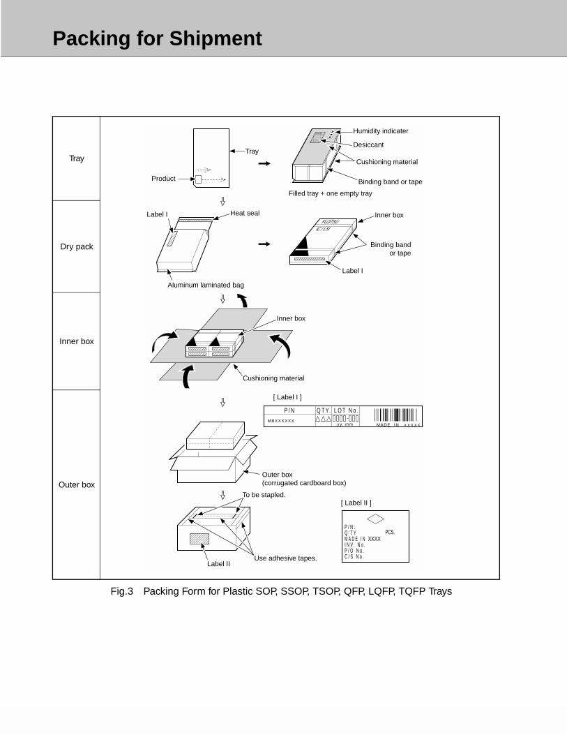
Packing for Shipment
3
Fig.3 Packing Form for Plastic SOP, SSOP, TSOP, QFP, LQFP, TQFP Trays
Tray
Dry pack
Inner box
Outer box
P / N :Q ' T YM A D E I N XXXXI N V . N o .P / O N o .C / S N o .
PCS.
P / NMBXXXXXX
yy. mm MADE IN x x x x x
Q T Y. L O T N o .
FUJITSUIC / LSI
[ Label II ]
[ Label I ]
Tray
Product
Humidity indicater
Desiccant
Cushioning material
Binding band or tape
Filled tray + one empty tray
Inner box
Binding bandor tape
Label I
Inner box
Cushioning material
Aluminum laminated bag
Heat sealLabel I
Outer box(corrugated cardboard box)
Label II
To be stapled.
Use adhesive tapes.
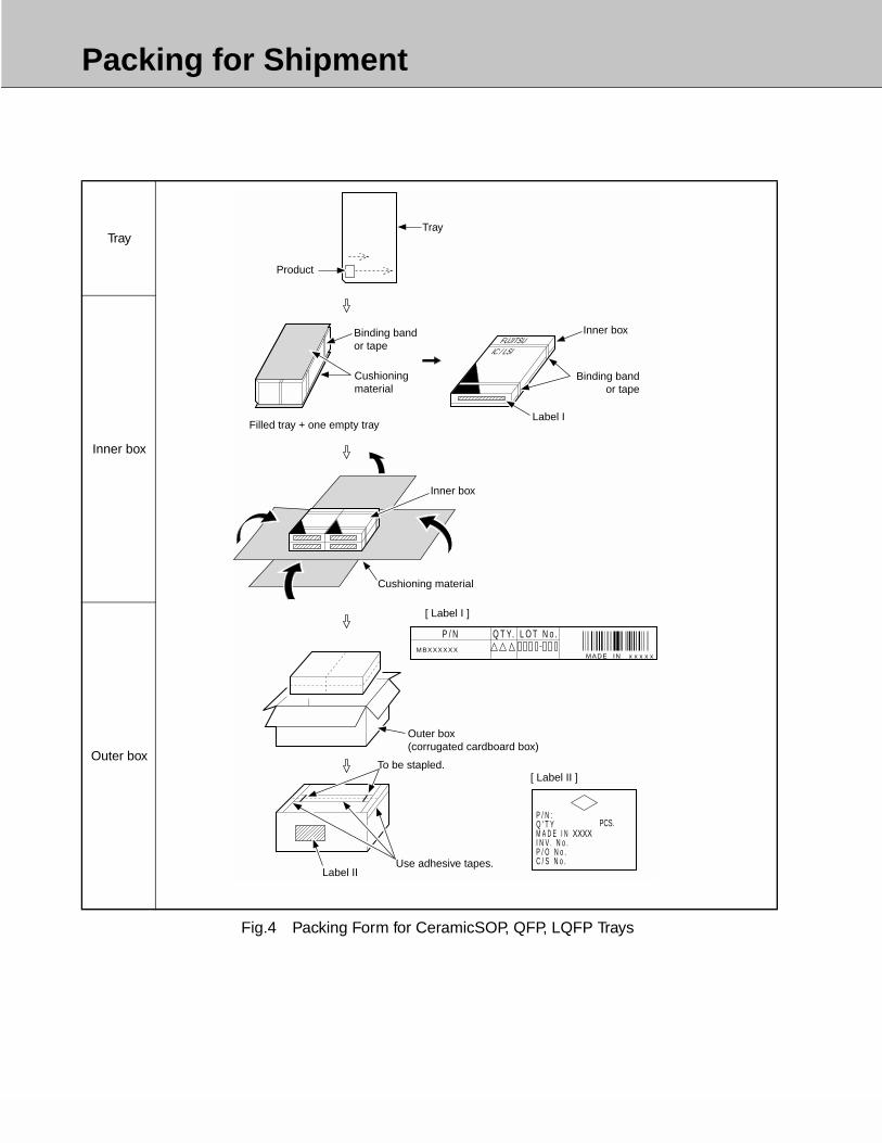
Packing for Shipment
4
Fig.4 Packing Form for CeramicSOP, QFP, LQFP Trays
Tray
Inner box
Outer box
P / N :Q ' T YM A D E I N XXXXI N V . N o .P / O N o .C / S N o .
PCS.
P / NMBXXXXXX
MADE IN x x x x x
Q T Y. L O T N o .
FUJITSUIC / LSI
[ Label II ]
[ Label I ]
Tray
Product
Inner box
Binding bandor tape
Label I
Inner box
Cushioning material
Outer box(corrugated cardboard box)
Label II
Binding bandor tape
Cushioningmaterial
Filled tray + one empty tray
To be stapled.
Use adhesive tapes.
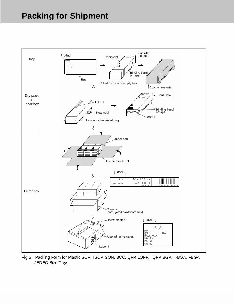
Packing for Shipment
5
Fig.5 Packing Form for Plastic SOP, TSOP, SON, BCC, QFP, LQFP, TQFP, BGA, T-BGA, FBGAJEDEC Size Trays
Tray
Dry pack↓
Inner box
Outer box
Product
Tray
Desiccant
Binding bandor tape
Humidityindicater
Cushion materialFilled tray + one empty tray
Label I
Heat seal
Aluminum laminated bag
FUJITSUIC / LSI
Binding bandor tape
Inner box
Label I
Inner box
Cushion material
Outer box(corrugated cardboard box)
To be stapled.
Use adhesive tapes.
Label II
P / N :Q ' T YMADE IN XXXXI N V . N o .P / O N o .C / S N o .
PCS.
P / NMBXXXXXX
yy. mm MADE IN x x x x x
Q T Y. L O T N o .
[ Label II ]
[ Label I ]

Packing for Shipment
6
Fig.6 Packing Form for Ceramic QFP, LQFP JEDEC Size Tray
Tray
Antistatic bag↓
Inner box
Outer box
Product
Tray
Binding bandor tape
Filled tray + one empty tray
Cushion material
FUJITSUIC / LSI
Binding bandor tape
Inner box
Label I
Inner box
Cushion material
Outer box(corrugated cardboard box)
To be stapled.
Use adhesive tapes.
Label II
P / N :Q ' T YMADE IN XXXXI N V . N o .P / O N o .C / S N o .
PCS.
P / NMBXXXXXX
yy. mm MADE IN x x x x x
Q T Y. L O T N o .
[ Label II ]
[ Label I ]
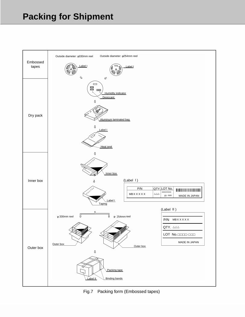
Packing for Shipment
7
Fig.7 Packing form (Embossed tapes)
Embossed tapes
Dry pack
Inner box
Outer box
Outside diameter: 330mm reel
FU
J I TS
U
Heat seal
Label I
Desiccant
Humidity indicator
Label I
Label I
Inner box
Aluminum laminated bag
φ 330mm reel φ 254mm reel
(Label )I
P/N
MB X X X X XMADE IN JAPAN
QTY. LOT No.
yy. mm
(Label )
P/N MB X X X X X
QTY.
LOT No.
MADE IN JAPAN
II
FU
J I TS
U
FU
J I TS
U
FU
J I TS
U
FU
J I TS
U
FU
J I TS
U
Label ITaping
Outer box
Label II
Packing tape
Binding bands
Outer box
φ Outside diameter: 254mm reelφ
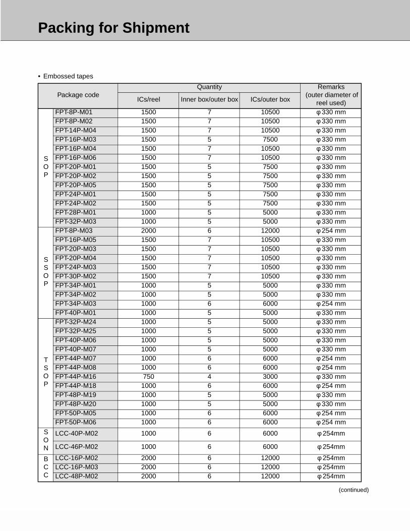
Packing for Shipment
8
• Embossed tapes
(continued)
Package codeQuantity Remarks
(outer diameter of reel used) ICs/reel Inner box/outer box ICs/outer box
SOP
FPT-8P-M01 1500 7 10500 φ 330 mmFPT-8P-M02 1500 7 10500 φ 330 mmFPT-14P-M04 1500 7 10500 φ 330 mmFPT-16P-M03 1500 5 7500 φ 330 mmFPT-16P-M04 1500 7 10500 φ 330 mmFPT-16P-M06 1500 7 10500 φ 330 mmFPT-20P-M01 1500 5 7500 φ 330 mmFPT-20P-M02 1500 5 7500 φ 330 mmFPT-20P-M05 1500 5 7500 φ 330 mmFPT-24P-M01 1500 5 7500 φ 330 mmFPT-24P-M02 1500 5 7500 φ 330 mmFPT-28P-M01 1000 5 5000 φ 330 mmFPT-32P-M03 1000 5 5000 φ 330 mm
SSOP
FPT-8P-M03 2000 6 12000 φ 254 mmFPT-16P-M05 1500 7 10500 φ 330 mmFPT-20P-M03 1500 7 10500 φ 330 mmFPT-20P-M04 1500 7 10500 φ 330 mmFPT-24P-M03 1500 7 10500 φ 330 mmFPT-30P-M02 1500 7 10500 φ 330 mmFPT-34P-M01 1000 5 5000 φ 330 mmFPT-34P-M02 1000 5 5000 φ 330 mmFPT-34P-M03 1000 6 6000 φ 254 mmFPT-40P-M01 1000 5 5000 φ 330 mm
TSOP
FPT-32P-M24 1000 5 5000 φ 330 mmFPT-32P-M25 1000 5 5000 φ 330 mmFPT-40P-M06 1000 5 5000 φ 330 mmFPT-40P-M07 1000 5 5000 φ 330 mmFPT-44P-M07 1000 6 6000 φ 254 mmFPT-44P-M08 1000 6 6000 φ 254 mmFPT-44P-M16 750 4 3000 φ 330 mmFPT-44P-M18 1000 6 6000 φ 254 mmFPT-48P-M19 1000 5 5000 φ 330 mmFPT-48P-M20 1000 5 5000 φ 330 mmFPT-50P-M05 1000 6 6000 φ 254 mmFPT-50P-M06 1000 6 6000 φ 254 mm
SON
LCC-40P-M02 1000 6 6000 φ 254mm
LCC-46P-M02 1000 6 6000 φ 254mm
BCC
LCC-16P-M02 2000 6 12000 φ 254mmLCC-16P-M03 2000 6 12000 φ 254mmLCC-48P-M02 2000 6 12000 φ 254mm
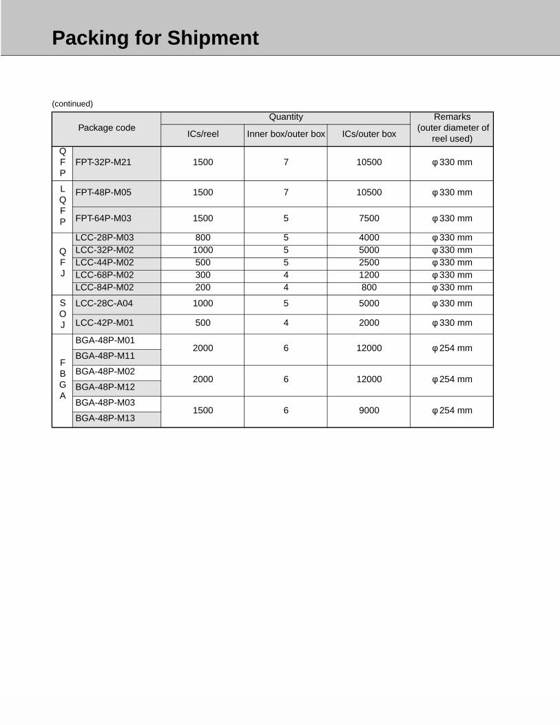
Packing for Shipment
9
(continued)
Package codeQuantity Remarks
(outer diameter of reel used) ICs/reel Inner box/outer box ICs/outer box
QFP
FPT-32P-M21 1500 7 10500 φ 330 mm
LQFP
FPT-48P-M05 1500 7 10500 φ 330 mm
FPT-64P-M03 1500 5 7500 φ 330 mm
QFJ
LCC-28P-M03 800 5 4000 φ 330 mmLCC-32P-M02 1000 5 5000 φ 330 mmLCC-44P-M02 500 5 2500 φ 330 mmLCC-68P-M02 300 4 1200 φ 330 mmLCC-84P-M02 200 4 800 φ 330 mm
SOJ
LCC-28C-A04 1000 5 5000 φ 330 mm
LCC-42P-M01 500 4 2000 φ 330 mm
FBGA
BGA-48P-M012000 6 12000 φ 254 mm
BGA-48P-M11
BGA-48P-M022000 6 12000 φ 254 mm
BGA-48P-M12
BGA-48P-M031500 6 9000 φ 254 mm
BGA-48P-M13

Packing for Shipment
10
6.1.2 Packing handling precautions
(1)Because corrugated cardboard boxes gradually weaken during storage as a result of
moisture, stacking, etc., inventory should be handled on a first-in, first-out basis.
(2)Although the IC packing materials (such as tubes) are designed to protect against elec-
trostatic damage, full precautions against electrostatic damage must be taken when
removing the products from their packing.
(3)Handle the inner and outer boxes gently. Rough handling can dislodge the tubes stop-
pers, allowing the products to fall out of the tubes and possibly bend their leads.
Rough handling of boxes containing ceramic packages in particular can cause chips,
cracks, or leak defects.
(4)Because the inner and outer boxes are made of corrugated cardboard, do not allow them
to become wet. Do not store the boxes outside or in a hot and humid location under any
circumstances.
(5)Do not throw, drop or otherwise roughly handle the outer boxes (corrugated cardboard
boxes) containing products under any circumstances.
(6)QFPs are packed in trays, but it is very easy to accidentally bend their leads when
removing them from their original packing and placing them in other packing. Therefore,
strictly obsever the following items.
a) When cutting the binding tape, hold the
trays securely in place with one hand.
b) Hold the trays firmly in place while removing the tape so that the trays do not shift
position. (If the trays shift, the packed ICs may be dislodged and the leads may bend.)
c) Check after packing the packages
Before stacking the trays containing the IC packages, check the following points.
•Make sure that the packages are properly positioned on the ribs.
•If any packages are not positioned on the ribs, , check for bent leads and then reposition
the packages.
Cut
Hand Use adhesive tapes
Tray

Packing for Shipment
11
Note: When handling the packages, make sure to take electrostatic countermeasures,
such as wearing finger sleeves or a grounded wrist strap. Use air tweezers, and
avoid touching the leads if possible.
d) Check after stacking the trays
•Make sure that there are no abnormal gaps between the stacked trays.
•Handle the stacked trays carefully when using packing tape or packing bands to secure
the trays. (Secure the trays only after making sure that there are no gaps.)
(7) When removing stoppers from containers, be careful not to let the stopper jump out of the
container.
(8) A container, coated with antistatic, may be sticky.
(9) Heat resistant tray has a label entitled "HT" or " heat proof temperature" (e.g. 125 °C
MAX). The heat resistant tray allows 125 °C heat being applied for 24 hours. It may cause
warp on heating or cooling. To minimize the warp, it is be heated or cooled on a flat surface.
Avoid the abrupt cooling.
Ribs(Correct) (If another tray is stacked on top of this one, the leads will be bent)
Is the package on top of the ribs?
Is the package centered properly?
Large gap
(Correct) (Incorrect)

Packing for Shipment
12
6.1.3 1st pin orientation of a package on the tray
QFP in general
Tray size and 1st pin orientation
PGA in general
Tray size and 1st pin orientation
F165
260
1st pin index
Chamfered corner
315
F
135.9
1st pin index
Chamfered corner
F
165
260
1st pin index
Chamfered corner
F
1st pin index
259
or 2
20
219 or 260
230.3
125.
3
F
1st pin index

Packing for Shipment
13
Tray size and 1st pin orientation
SOP in general
TSOPI
TSOPII
BGAT-BGAFBGASONBCC
F
165
260
1st pin indexChamfered corner
F
165
260
Chamfered corner = Positive bend 1st pin index = Reverse bend 1st pin index
F
135.9
315
Chamfered corner = Positive bend 1st pin index = Reverse bend 1st pin index
F
165
260
Chamfered corner = Positive bend 1st pin index = Reverse bend 1st pin index
F135.9
315
Chamfered corner
= Positive bend 1st pin index = Reverse bend 1st pin index
F
135.9
315
1st pin indexChamfered corner
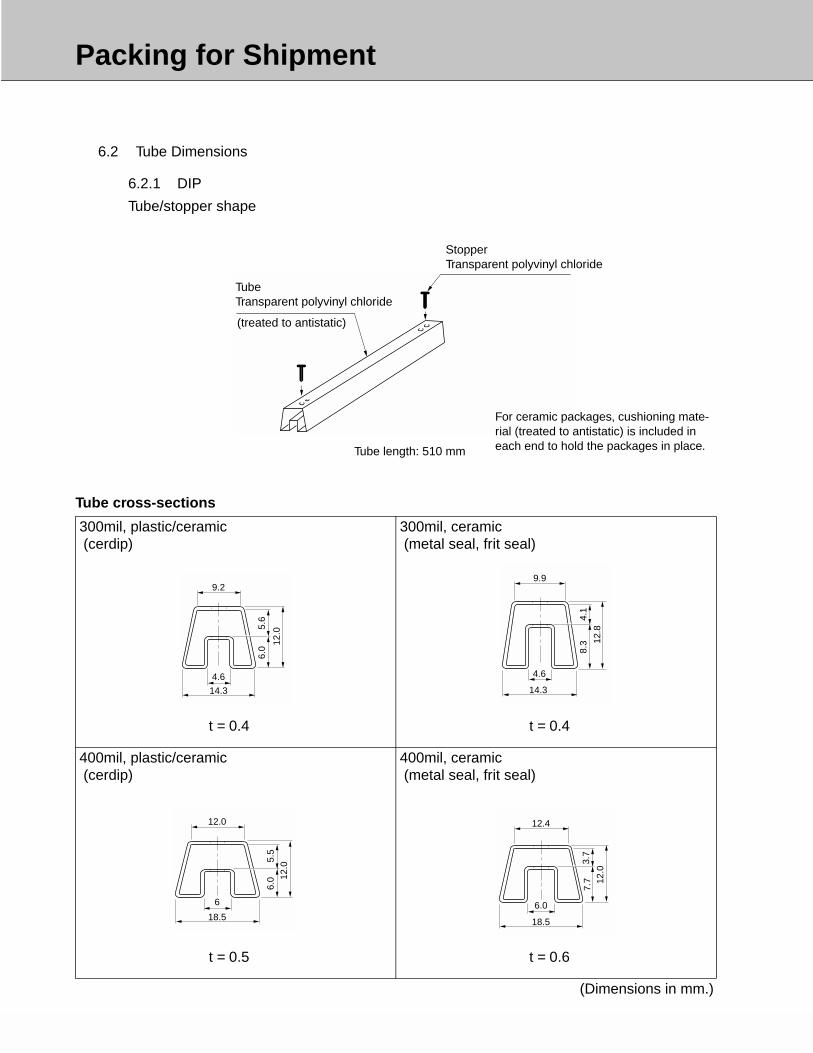
Packing for Shipment
14
6.2 Tube Dimensions
6.2.1 DIP
Tube/stopper shape
Tube cross-sections
300mil, plastic/ceramic (cerdip)
300mil, ceramic (metal seal, frit seal)
400mil, plastic/ceramic (cerdip)
400mil, ceramic (metal seal, frit seal)
(Dimensions in mm.)
For ceramic packages, cushioning mate-rial (treated to antistatic) is included in each end to hold the packages in place.
StopperTransparent polyvinyl chloride
TubeTransparent polyvinyl chloride
(treated to antistatic)
Tube length: 510 mm
14.3
4.6
12.05.
66.
0
9.2
t = 0.4
14.3
4.6
12.8
4.1
8.3
9.9
t = 0.4
18.5
6
12.0
5.5
6.0
12.0
t = 0.5
18.5
6.0
12.0
3.7
7.7
12.4
t = 0.6

Packing for Shipment
15
Tube cross-sections
600mil, plastic/ceramic (cerdip)
600mil, ceramic (metal seal, frit seal)
750mil, plastic
(Dimensions in mm.)
23.0
11.4
16.0
5.5
10.0
18.0
t = 0.5
23.0
11.4
13.9
3.4
10.0
18.5
t = 0.5
26.0
16.0
12.55.
96.
0
21.8
t = 0.6

Packing for Shipment
16
Maximum quantity per tube (DIP)
Package form Package codeMaximum quantity
pcs/tube pcs/inner box pcs/outer box
DIP, 300mil, plastic/ceramic (cerdip)
DIP-8P-M01 50 2000 8000DIP-14P-M02 25 1000 4000DIP-14C-C01 25 1000 4000DIP-14C-C04 25 1000 4000DIP-16P-M03 25 1000 4000DIP-16P-M04 25 1000 4000DIP-16P-M05 25 1000 4000DIP-16C-C01 25 1000 4000DIP-16C-C02 25 1000 4000DIP-16C-C04 25 1000 4000DIP-18P-M02 22 880 3520DIP-18P-M03 22 880 3520DIP-18P-M04 22 880 3520DIP-18C-C01 21 840 3360DIP-20P-M01 20 800 3200DIP-20P-M02 20 800 3200DIP-20P-M03 20 800 3200DIP-20C-C01 20 800 3200DIP-22P-M04 18 720 2880DIP-22C-C03 17 680 2720DIP-24P-M03 16 640 2560DIP-24P-M05 22 880 3520DIP-24C-C04 15 600 2400DIP-28P-M04 13 520 2080DIP-32P-M02 12 480 1920
DIP, 300mil, ceramic (metal seal, frit seal)
DIP-20C-A01 20 800 3200
DIP, 400mil, plastic/ceramic (cerdip)
DIP-20C-C02 20 600 2400DIP-22P-M03 18 540 2160DIP-22C-C02 17 510 2040DIP-24P-M04 16 480 1920DIP-28P-M03 18 540 2160DIP-28P-M06 13 390 1560
DIP, 400mil, ceramic (metal seal, frit seal)
DIP-24C-A05 16 480 1920DIP-28C-A10 13 390 1560DIP-32C-A02 12 360 1440
DIP, 600mil, plastic/ceramic (cerdip)
DIP-24P-M02 16 320 1280DIP-24C-C01 15 300 1200

Packing for Shipment
17
Maximum quantity per tube (DIP)
Package form Package codeMaximum quantity
pcs/tube pcs/inner box pcs/outer box
DIP, 600mil, plastic/ceramic (cerdip)
DIP-24C-C03 15 300 1200DIP-28C-C02 13 260 1040DIP-32P-M01 12 240 960DIP-36P-M01 10 200 800DIP-40P-M02 9 180 720DIP-40P-M03 12 240 960DIP-42P-M02 12 240 960DIP-42P-M03 9 180 720DIP-48P-M01 11 220 880DIP-48P-M02 8 160 640DIP-52P-M01 10 200 800
DIP, 600mil, ceramic (metal seal, frit seal)
DIP-24C-A04 16 320 1280DIP-24C-A06 16 320 1280DIP-24C-A07 16 320 1280DIP-28C-A01 13 260 1040DIP-28C-A07 13 260 1040DIP-40C-A04 9 180 720DIP-40C-A05 9 180 720DIP-42C-A01 9 180 720DIP-42C-A03 9 180 720DIP-48C-A01 8 160 640
DIP, 750mil, plastic DIP-64P-M01 8 160 640
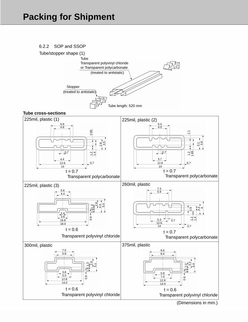
Packing for Shipment
18
6.2.2 SOP and SSOP
Tube/stopper shape (1)
Tube cross-sections225mil, plastic (1)
Transparent polycarbonate
225mil, plastic (2)
Transparent polycarbonate
225mil, plastic (3)
Transparent polyvinyl chloride
260mil, plastic
Transparent polycarbonate
300mil, plastic
Transparent polyvinyl chloride
375mil, plastic
Transparent polyvinyl chloride
(Dimensions in mm.)
(treated to antistatic)
(treated to antistatic) Stopper
TubeTransparent polyvinyl chloride or Transparent polycarbonate
Tube length: 520 mm
1412.6
0.7
4.4
3.5
4.65.9
2.8
1.4
1.2
0.85
0.7
t = 0.714
12.6
0.7
3.7
3.8
4.05.4
3.1
1.651.2
1.1
0.7
t = 0.7
5.0
4.4
5.64.4
2.43.616.818.0
2.8
1.6
0.6
1.3
t = 0.614
12.60.75.3
4
5.97.3
3.3
1.4
1.2
0.7
0.9
t = 0.7
5.1
7.05.8
3.85.012.814.0
2.9
1.6
0.6
1.3
t = 0.6
5.4
9.68.4
5.87.012.814.0
3.2
1.6
0.6
2.0
t = 0.6

Packing for Shipment
19
450mil, plastic (1)
Transparent polycarbonate
450mil, plastic (2)
Transparent polyvinyl chloride
(Dimensions in mm.)
15.6
6.88.014.4
5.4
1.6
1.7 3.2
10.69.4
t = 0.6
5.4
10.69.4
6.88.014.415.6
3.2
1.6
0.6
2.0
t = 0.6

Packing for Shipment
20
Tube/stopper shape (2)
Tube cross-sections
525mil, plastic
(Dimensions in mm.)
TubeTransparent polycarbonate (treated to antistatic)
Tube length: 510 mm
(treated to antistatic)
Stopper
12.00.8
0.8
3.0
5.4
9.0
10.616.418.0
t = 0.8

Packing for Shipment
21
Maximum quantity per tube (SOP and SSOP)
Package form Package codeMaximum quantity
pcs/tube pcs/inner box pcs/outer box
SOP/SSOP, 225mil, plastic (1) FPT-8P-M03 130 10400 41600FPT-16P-M05 95 7600 30400FPT-20P-M03 75 6000 24000
SOP/SSOP, 225mil, plastic (2) FPT-8P-M02 95 7600 30400SOP/SSOP, 225mil, plastic (3) FPT-14P-M03 50 4000 16000
FPT-16P-M04 48 3840 15360SOP/SSOP, 260mil, plastic FPT-24P-M03 62 4960 19840
FPT-30P-M02 50 4000 16000SOP/SSOP, 300mil, plastic FPT-8P-M01 80 6400 25600
FPT-14P-M04 50 4000 16000FPT-16P-M06 50 4000 16000FPT-16C-C02 50 4000 16000FPT-20P-M01 40 3200 12800FPT-24P-M01 33 2640 10560
SOP/SSOP, 375mil, plastic FPT-16P-M03 39 3120 12480FPT-20P-M02 39 3120 12480FPT-20P-M05 39 3120 12480FPT-24P-M02 33 2640 10560FPT-28P-M01 28 2240 8960FPT-34P-M01 28 2240 8960FPT-34P-M02 28 2240 8960
SOP/SSOP, 450mil, plastic (1) FPT-32P-M02 24 1920 7680FPT-40P-M04 28 2240 8960FPT-40P-M05 28 2240 8960
SOP/SSOP, 450mil, plastic (2) FPT-40P-M01 28 2240 8960SOP/SSOP, 525mil, plastic FPT-32P-M03 23 1150 4600
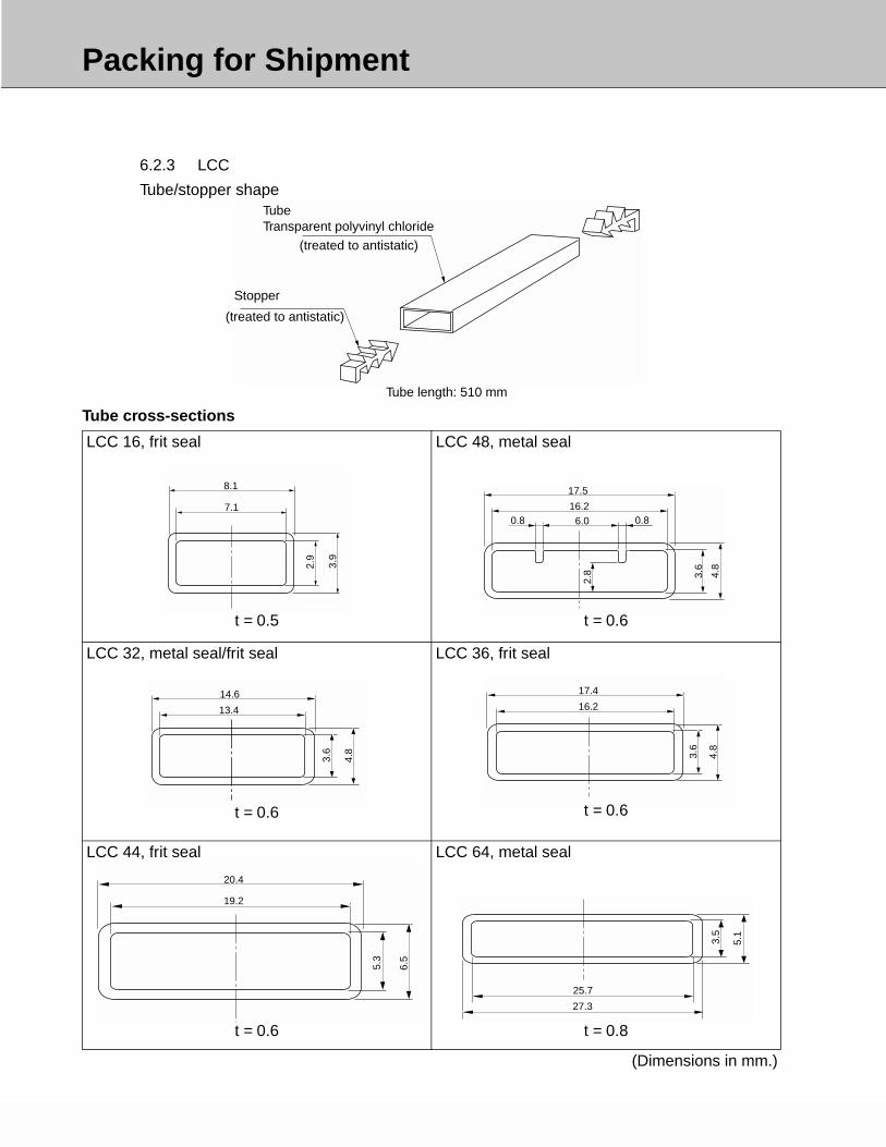
Packing for Shipment
22
6.2.3 LCC
Tube/stopper shape
Tube cross-sections
LCC 16, frit seal LCC 48, metal seal
LCC 32, metal seal/frit seal LCC 36, frit seal
LCC 44, frit seal LCC 64, metal seal
(Dimensions in mm.)
TubeTransparent polyvinyl chloride
(treated to antistatic)
Tube length: 510 mm
(treated to antistatic)
Stopper
8.1
7.1
2.9
3.9
t = 0.5
16.2
17.5
6.0 0.80.8
3.6
4.8
2.8
t = 0.6
4.8
14.6
13.4
3.6
t = 0.6
4.8
17.4
16.23.
6
t = 0.6
6.5
20.4
19.2
5.3
t = 0.6
3.5
27.3
25.7
5.1
t = 0.8

Packing for Shipment
23
Maximum quantity per tube (LCC)
Package form Package codeMaximum quantity
pcs/tube pcs/inner box pcs/outer box
LCC16, frit seal LCC-16C-F01 77 7700 30800LCC 48, metal seal LCC-48C-A01 34 2040 8160LCC 32, metal seal/frit seal LCC-32C-F01 35 2450 9800LCC 36, frit seal LCC-36C-F01 35 2450 9800LCC 44, frit seal LCC-44C-F01 28 1260 5040LCC 64, metal seal LCC-64C-A01 26 832 3328

Packing for Shipment
24
6.2.4 QFJ
Tube/stopper shape
Tube cross-sections
QFJ 28, plastic QFJ 32, plastic/ceramic
QFJ 44, ceramic QFJ 44, plastic
QFJ 68, plastic QFJ 84, plastic
(Dimensions in mm.)
TubeTransparent polyvinyl chloride
(treated to antistatic)
Tube length: 510 mm
StopperTransparent polyvinyl chloride
Cushioning material(treated to antistatic) is included in each end to hold the packages in place.
6.5
15.3
14.1
5.3
t = 0.615.3
14.1
5.5
4.3
t = 0.6
20.4
19.2
6.3
5.1
t = 0.6
20.4
19.2
6.5
5.3
t = 0.6
28.0
26.8
6.5
5.3
t = 0.6
33.1
31.9
6.5
5.3
t = 0.6

Packing for Shipment
25
Maximum quantity per tube (QFJ)
Package form Package codeMaximum quantity
pcs/tube pcs/inner box pcs/outer box
QFJ 28, plastic LCC-28P-M03 36 2016 8064QFJ 32, plastic/ceramic LCC-32P-M02 30 1680 6720
QFJ-32C-C01 30 1680 6720QFJ 44, ceramic QFJ-44C-C01 25 1000 4000QFJ 44, plastic LCC-44P-M02 25 1000 4000QFJ 68, plastic LCC-68P-M02 17 544 2176QFJ 84, plastic LCC-84P-M02 14 336 1344

Packing for Shipment
26
6.2.5 SOJ
Tube/stopper shape
Tube cross-sections
Maximum quantity per tube (SOJ)
400mil, plastic/metal seal
(Dimensions in mm.)
Package form Package codeMaximum quantity
pcs/tube pcs/inner box pcs/outer box
SOJ 28 (400mil) ,plastic/metal seal
LCC-28C-A04 26 1560 6240LCC-42P-M01 17 1020 4080
TubeTransparent polyvinyl chloride
(treated to antistatic)
Tube length: 510 mm
(treated to antistatic)
Stopper
13.3
6.8
2.0
6.0
0.6
t = 0.6

Tray Dimensions
27
6.3 Tray Dimensions
6.3.1 Plastic SOP • SOP • TSOP (heat proof type) , ceramic SOP (non-heat proof type)
(1) Plastic SOPSOP38(The identical Figure is also in Plastic QFP 64, 80, 100.)
PKG codeMaximum strage capacity
pcs/tray pcs/inner box pcs/outer box
FPT-38P-M02 40 400 1600
Material: Conductive polypropyleneHeat proof temperature: 125 °C MAX
SOP 44 PKG codeMaximum strage capacity
pcs/tray pcs/inner box pcs/outer box
FPT-44P-M16 40 400 1600
Material: Conductive polyphenylenetherHeat proof temperature: 125 °C MAX
(Dimensions in mm)
260.0
31.0×7 = 217.021.5
165.
0
32.0
×4 =
128
.018
.5
6.5
26.720.4
20.7
14.4
14 – NO HOLES
26 – φ10 HOLES
260.0
31.0×7 = 217.021.5
165.
0
32.0
×4 =
128
.018
.5
6.5
28.2
17.0
10 – NO HOLES
30 – HOLES

Tray Dimensions
28
(2) Ceramic SOP (non-heat proof type) SOP 24 PKG code
Maximum strage capacity
pcs/tray pcs/inner box pcs/outer box
FPT-24C-F01 40 400 1600
Material: Conductive polystyreneHeat proof temperature: 50 °C MAX
(Dimensions in mm)
260.0
30×7 = 210.025.0
165.
0
30×4
= 1
20.0
22.5
6.5
14.8
23.2
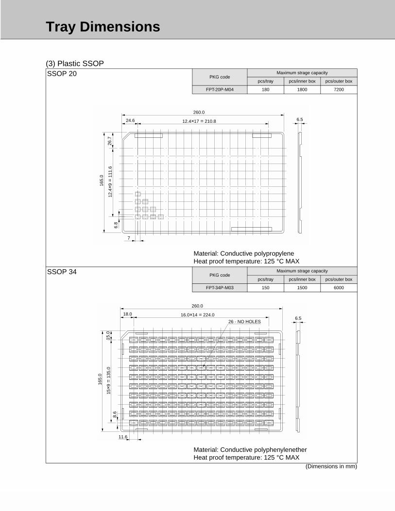
Tray Dimensions
29
(3) Plastic SSOPSSOP 20 PKG code
Maximum strage capacity
pcs/tray pcs/inner box pcs/outer box
FPT-20P-M04 180 1800 7200
Material: Conductive polypropyleneHeat proof temperature: 125 °C MAX
SSOP 34 PKG codeMaximum strage capacity
pcs/tray pcs/inner box pcs/outer box
FPT-34P-M03 150 1500 6000
Material: Conductive polyphenylenetherHeat proof temperature: 125 °C MAX
(Dimensions in mm)
260.0
12.4×17 = 210.824.6
165.
0
12.4
×9 =
111
.626
.7
6.5
7
6.8
260.0
16.0×14 = 224.018.0
165.
0
15×9
= 1
35.0
15.0
6.5
11.6
8.6
26 - NO HOLES

Tray Dimensions
30
SSOP 56 PKG codeMaximum strage capacity
pcs/tray pcs/inner box pcs/outer box
FPT-56P-M03 66 660 3960
Material: Conductive polyphenylenetherHeat proof temperature: 125 °C MAX
(Dimensions in mm)
135.
9
21.
9×5
= 10
9.5
13.2
13.2
16.53.8
28.2×10 = 282
322.6315
7.6216.53.8
23.75
16.6
4-NO HOLES
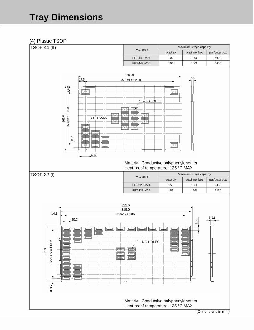
Tray Dimensions
31
(4) Plastic TSOPTSOP 44 (II) PKG code
Maximum strage capacity
pcs/tray pcs/inner box pcs/outer box
FPT-44P-M07 100 1000 4000
FPT-44P-M08 100 1000 4000
Material: Conductive polyphenylenetherHeat proof temperature: 125 °C MAX
TSOP 32 (I) PKG codeMaximum strage capacity
pcs/tray pcs/inner box pcs/outer box
FPT-32P-M24 156 1560 9360
FPT-32P-M25 156 1560 9360
Material: Conductive polyphenylenetherHeat proof temperature: 125 °C MAX
(Dimensions in mm)
260.0
25.0×9 = 225.017.5
165.
0
15.0
×9 =
135
.015
.0
18.2
6.5
12.0
16 – NO HOLES
84 – HOLES
135.
9
12×9
.85
= 11
8.2
8.85
14.5
20.3
11×26 = 286
322.6315.0
8.4
7.62
10 − NO HOLES
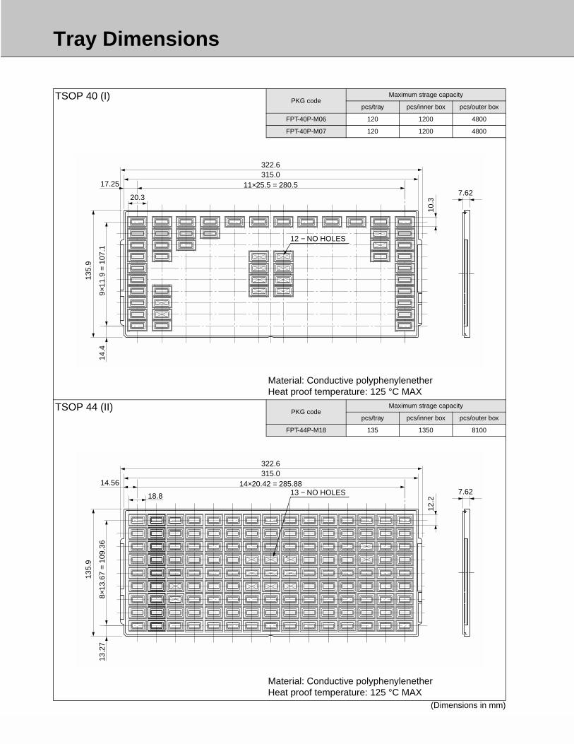
Tray Dimensions
32
TSOP 40 (I) PKG codeMaximum strage capacity
pcs/tray pcs/inner box pcs/outer box
FPT-40P-M06 120 1200 4800
FPT-40P-M07 120 1200 4800
Material: Conductive polyphenylenetherHeat proof temperature: 125 °C MAX
TSOP 44 (II) PKG codeMaximum strage capacity
pcs/tray pcs/inner box pcs/outer box
FPT-44P-M18 135 1350 8100
Material: Conductive polyphenylenetherHeat proof temperature: 125 °C MAX
(Dimensions in mm)
135.
9
9×11
.9 =
107
.114
.4
17.25 11×25.5 = 280.5
322.6315.0
10.3
7.6220.3
12 − NO HOLES
135.
9
8×13
.67
= 10
9.36
13.2
7
14.56
18.8
14×20.42 = 285.88
322.6315.0
12.2
7.6213 − NO HOLES

Tray Dimensions
33
TSOP 48 (I) PKG codeMaximum strage capacity
pcs/tray pcs/inner box pcs/outer box
FPT-48P-M19 96 960 5760
FPT-48P-M20 96 960 5760
Material: Conductive polyphenylenetherHeat proof temperature: 125 °C MAX
TSOP 50 (II) PKG codeMaximum strage capacity
pcs/tray pcs/inner box pcs/outer box
FPT-50P-M05 117 1170 7020
FPT-50P-M06 117 1170 7020
Material: Conductive polyphenylenetherHeat proof temperature: 135 °C MAX
(Dimensions in mm)
135.
9
7×14
.9 =
104
.315
.8
322.6
315.011×25.5 = 280.517.25
12.3
7.6220.3
8 − NO HOLES
12×22.96 = 275.5219.74
135.
9
8 ×13
.67
= 10
9.36
13.2
7
12.0
2
7.62
322.6315.0
21.35 13 – NO HOLES

Tray Dimensions
34
TSOP 54 (II) PKG codeMaximum strage capacity
pcs/tray pcs/inner box pcs/outer box
FPT-54P-M01 84 840 5040
Material: Conductive polyphenylenetherHeat proof temperature: 125 °C MAX
TSOP 54, 86 (II) PKG codeMaximum strage capacity
pcs/tray pcs/inner box pcs/outer box
FPT-54P-M02 108 1080 6480
FPT-86P-M01 108 1080 6480
Material: Conductive polyphenylenetherHeat proof temperature: 125 °C MAX
(Dimensions in mm)
7.62
14.6
24.18 11×24.24 = 266.64
322.6315.0
135.
9
6×16
.21
= 97
.26
19.3
2
10 − NO HOLES
22.7
135.
9
8×14
.0 =
112
.00
12.0
0
21.70 11×24.70 = 271.70
322.6315.0
12.2
0 7.6210 − NO HOLES22.72

Tray Dimensions
35
TSOP 56 (I) PKG codeMaximum strage capacity
pcs/tray pcs/inner box pcs/outer box
FPT-56P-M01 91 910 5460
FPT-56P-M02 91 910 5460
Material: Conductive polyphenylenetherHeat proof temperature: 125 °C MAX
TSOP 56 (I) PKG codeMaximum strage capacity
pcs/tray pcs/inner box pcs/outer box
FPT-56P-M04 128 1280 7680
Material: Conductive polyphenylenetherHeat proof temperature: 125 °C MAX
(Dimensions in mm)
135.
9
18.1
56×
16.6
= 9
9.6
18.5
322.6315
12×22.9 = 274.87.62
20.1
3.8
20.1514.2
3.8
20.1
13-NO HOLES
135.
9
7×14
.9 =
104
.315
.8
12.2
15.8
15×19.0 = 285
322.6315.0
7.62
153.83.8
15
14.2
8-NO HOLES

Tray Dimensions
36
6.3.2 Plastic SON (heat proof type)
SON 40 PKG codeMaximum strage capacity
pcs/tray pcs/inner box pcs/outer box
LCC-40P-M02 230 2300 13800
Material: Conductive polyphenylenetherHeat proof temperature: 125 °C MAX
SON 46 PKG codeMaximum strage capacity
pcs/tray pcs/inner box pcs/outer box
LCC-46P-M02 210 2100 12600
Material: Conductive polyphenylenetherHeat proof temperature: 125 °C MAX
(Dimensions in mm)
135.
9
9×12
.5 =
112
.50
11.7
0
10.10 22×13.4 = 294.80
322.6315.0
10.3 7.6216 − NO HOLES11.4
135.
9
9×12
.5 =
112
.50
11.7
0
11.50 20×14.6 = 292.00
322.6315.0
10.3
7.6216 − NO HOLES12.65
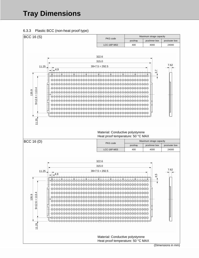
Tray Dimensions
37
6.3.3 Plastic BCC (non-heat proof type)
BCC 16 (S) PKG codeMaximum strage capacity
pcs/tray pcs/inner box pcs/outer box
LCC-16P-M02 400 4000 24000
Material: Conductive polystyreneHeat proof temperature: 50 °C MAX
BCC 16 (D) PKG codeMaximum strage capacity
pcs/tray pcs/inner box pcs/outer box
LCC-16P-M03 400 4000 24000
Material: Conductive polystyreneHeat proof temperature: 50 °C MAX
(Dimensions in mm)
11.2
59×
12.6
= 1
13.4
135.
9
39×7.5 = 292.5
315.07.62
322.6
11.25
3.74.9
11.2
59×
12.6
= 1
13.4
135.
9
39×7.5 = 292.5
315.07.62
322.6
11.25
4.54.9
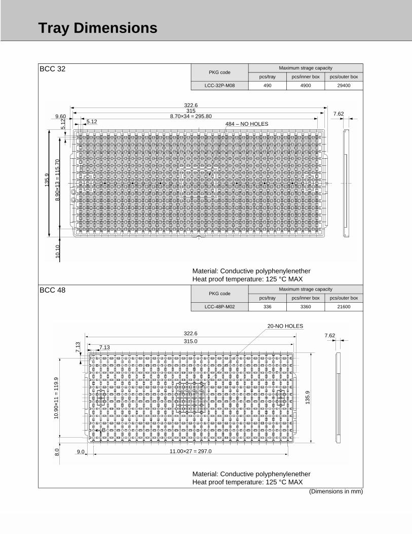
Tray Dimensions
38
BCC 32 PKG codeMaximum strage capacity
pcs/tray pcs/inner box pcs/outer box
LCC-32P-M08 490 4900 29400
Material: Conductive polyphenylenetherHeat proof temperature: 125 °C MAX
BCC 48 PKG codeMaximum strage capacity
pcs/tray pcs/inner box pcs/outer box
LCC-48P-M02 336 3360 21600
Material: Conductive polyphenylenetherHeat proof temperature: 125 °C MAX
(Dimensions in mm)
7.629.60 8.70×34 = 295.80315
322.6
135.
9
10.1
08.
90×1
3 =
115.
70
5.12
5.12 484 – NO HOLES
20-NO HOLES
135.
9
322.6315.0
8.0
10.9
0×11
= 1
19.9
11.00×27 = 297.09.0
02 02 02 02
B
7.62
7.13
7.13

Tray Dimensions
39
6.3.4 Plastic QFP • LQFP • TQFP (heat proof type)
(1) Plastic QFPQFP 64, 80, 100(The identical Figure is also in Plastic SOP38.)
PKG codeMaximum strage capacity
pcs/tray pcs/inner box pcs/outer box
FPT-64P-M06 40 400 1600
FPT-64P-M10 40 400 1600
FPT-80P-M06 40 400 1600
FPT-80P-M07 40 400 1600
FPT-100P-M06 40 400 1600
FPT-100P-M07 40 400 1600
Material: Conductive polypropyleneHeat proof temperature: 125 °C MAX
QFP 80, 176 PKG codeMaximum strage capacity
pcs/tray pcs/inner box pcs/outer box
FPT-80P-M09 15 120 480
FPT-176P-M01 15 120 480
Material: Conductive polyphenylenetherHeat proof temperature: 125 °C MAX
(Dimensions in mm)
260.0
31.0×7 = 217.021.5
165.
0
32.0
×4 =
128
.018
.5
6.5
26.720.4
20.7
14.4
14 – NO HOLES
26 – φ10 HOLES
27.2
260.0
30.09.5
50.0×4 = 200.0
52.0
×2 =
104
.030
.5
27.2
165.
0
5 – NO HOLES 10 – HOLES
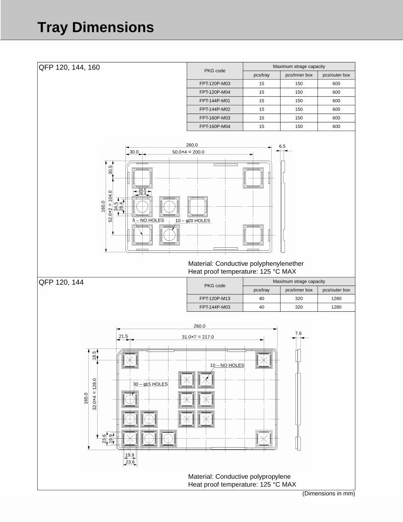
Tray Dimensions
40
QFP 120, 144, 160 PKG codeMaximum strage capacity
pcs/tray pcs/inner box pcs/outer box
FPT-120P-M03 15 150 600
FPT-120P-M04 15 150 600
FPT-144P-M01 15 150 600
FPT-144P-M02 15 150 600
FPT-160P-M03 15 150 600
FPT-160P-M04 15 150 600
Material: Conductive polyphenylenetherHeat proof temperature: 125 °C MAX
QFP 120, 144 PKG codeMaximum strage capacity
pcs/tray pcs/inner box pcs/outer box
FPT-120P-M13 40 320 1280
FPT-144P-M03 40 320 1280
Material: Conductive polypropyleneHeat proof temperature: 125 °C MAX
(Dimensions in mm)
260.0
50.0×4 = 200.030.0
165.
0
52.0
×2 =
104
.030
.5
6.5
34.5
34.528.4
28.4
10 – φ20 HOLES5 – NO HOLES
260.0
21.57.6
31.0×7 = 217.0
32.0
×4 =
128
.0
165.
0
18.5
23.6
19.9
23.6
19.9
30 – φ15 HOLES
10 – NO HOLES

Tray Dimensions
41
QFP 160, 208, 256 PKG codeMaximum strage capacity
pcs/tray pcs/inner box pcs/outer box
FPT-160P-M11 24 240 1440
FPT-208P-M04 24 240 1440
FPT-256P-M09 24 240 1440
Material: Conductive polyphenylenetherHeat proof temperature: 125 °C MAX
QFP 208, 256 PKG codeMaximum strage capacity
pcs/tray pcs/inner box pcs/outer box
FPT-208P-M01 15 120 480
FPT-256P-M06 15 120 480
Material: Conductive polypropyleneHeat proof temperature: 125 °C MAX
(Dimensions in mm)
315.0
7×37.02 = 259.14
4 − NO HOLE
27.93
135.
9
2×37
.02
= 74
.04
7.62
30.9
3
34.027.5
34.0
27.5
322.6
260.0
30.09.5
50.0×4 = 200.0
165.
0
52.0
×2 =
104
.030
.5
31.2
31.2
10 – HOLES 5 – NO HOLES

Tray Dimensions
42
QFP 232 PKG codeMaximum strage capacity
pcs/tray pcs/inner box pcs/outer box
FPT-232P-M01 15 120 480
Material: Conductive polypropyleneHeat proof temperature: 125 °C MAX
QFP 240, 296 PKG codeMaximum strage capacity
pcs/tray pcs/inner box pcs/outer box
FPT-240P-M02 15 120 480
FPT-296P-M01 15 120 480
Material: Conductive polypropyleneHeat proof temperature: 125 °C MAX
(Dimensions in mm)
260.0
50.0×4 = 200.0
165.
0
52.0
×2 =
104
.030
.530
.5
7.645
.5
40.2
30.0
45.5
40.2
5 – NO HOLES
10 – φ20 HOLES
260.0
30.07.6
30.5
165.
0
35.6
31.9
35.631.9
50.0×4 = 200.0
52.0
×2 =
104
.0
10 – φ27 HOLES5 – NO HOLES

Tray Dimensions
43
QFP 240 PKG codeMaximum strage capacity
pcs/tray pcs/inner box pcs/outer box
FPT-240P-M03 24 240 1440
Material: Conductive polypropyleneHeat proof temperature: 125 °C MAX
QFP 304 PKG codeMaximum strage capacity
pcs/tray pcs/inner box pcs/outer box
FPT-304P-M02 12 120 720
Material: Conductive polyphenylenetherHeat proof temperature: 125 °C MAX
(Dimensions in mm)
322.6
315.0
7×37.82 = 264.725.13
135.
9
41.3
8×2
= 82
.8
7.62
26.5
7
36.20
31.58
36.2
0
31.5
8
4 – NO HOLES
7.6231.1 50.56×5 = 252.8
315.0
322.6
135.
9
29.2
277
.46
44.5
44.5

Tray Dimensions
44
(2) Plastic LQFP (LQFP is a Fujitsu package name.) LQFP 32, 48 PKG code
Maximum strage capacity
pcs/tray pcs/inner box pcs/outer box
FPT-32P-M21 40 400 1600
FPT-48P-M05 40 400 1600
Material: Conductive polypropyleneHeat proof temperature: 125 °C MAX
LQFP 64, TQFP 64 PKG codeMaximum strage capacity
pcs/tray pcs/inner box pcs/outer box
FPT-64P-M03 40 400 1600
FPT-64P-M04 40 400 1600
Material: Conductive polypropyleneHeat proof temperature: 125 °C MAX
(Dimensions in mm)
260.0
31.0×7 = 217.0
165.
0
32.0
×4 =
128
.018
.5
6.521.5
9.37.05
9.3
7.05
30 – φ8 HOLES
10 – NO HOLES
260.0
31.0×7 = 217.0
165.
0
32.0
×4 =
128
.018
.5
6.521.5
12.3
9.85
12.39.85
10 – NO HOLES
30 – φ8 HOLES

Tray Dimensions
45
LQFP 64, 80 PKG codeMaximum strage capacity
pcs/tray pcs/inner box pcs/outer box
FPT-64P-M09 40 400 1600
FPT-80P-M05 40 400 1600
Material: Conductive polypropyleneHeat proof temperature: 125 °C MAX
LQFP 80, 100, 120, TQFP 100, 120 PKG codeMaximum strage capacity
pcs/tray pcs/inner box pcs/outer box
FPT-80P-M11 40 400 1600
FPT-100P-M05 40 400 1600
FPT-100P-M09 40 400 1600
FPT-120P-M05 40 400 1600
FPT-120P-M17 40 400 1600
Material: Conductive polypropyleneHeat proof temperature: 125 °C MAX
(Dimensions in mm)
165.
0
18.5
32.0
×4 =
128
.0
14.3
11.8
531.0×7 = 217.0
260.0
21.56.5
14.3
11.85
10 – NO HOLES
30 – φ10 HOLES
260.0
21.56.5
31.0×7 = 217.0
32.0
×4 =
128
.0
165.
0
18.5 16
.3
13.8
5
16.3
13.85
10 – NO HOLES
30 – φ12 HOLES

Tray Dimensions
46
LQFP 144, 176 PKG codeMaximum strage capacity
pcs/tray pcs/inner box pcs/outer box
FPT-144P-M08 60 600 3600
FPT-176P-M03 60 600 3600
Material: Conductive polyphenylenetherHeat proof temperature: 125 °C MAX
LQFP 144 PKG codeMaximum strage capacity
pcs/tray pcs/inner box pcs/outer box
FPT-144P-M12 84 840 5040
Material: Conductive polyphenylenetherHeat proof temperature: 125 °C MAX
(Dimensions in mm)
7.62
25.2
×4 =
100
.817
.55
135.
9
2319
.85
17.8 25.4×11 = 279.4315.0322.6
2319.85
8 – NO HOLES
315.0
8-NO HOLES22.10×13 = 287.3
135.
921
.90×
5 =
109.
513
.2
13.853.8
13.2
15.8
5
7.6213.85
3.8
322.6
18.5
18.5
15.85

Tray Dimensions
47
LQFP 176 PKG codeMaximum strage capacity
pcs/tray pcs/inner box pcs/outer box
FPT-176P-M02 40 400 2400
Material: Conductive polyphenylenetherHeat proof temperature: 125 °C MAX
LQFP 208 PKG codeMaximum strage capacity
pcs/tray pcs/inner box pcs/outer box
FPT-208P-M06 36 360 2160
Material: Conductive polyphenylenetherHeat proof temperature: 125 °C MAX
(Dimensions in mm)
315.0
9×30.4 = 273.620.7
135.
9
3×31
.50
= 94
.520
.7
7.62
322.6
26.16
23.90
26.1
623
.90
6-NO HOLES
7.62
32.2
0×3
= 96
.619
.65
19.6
5
135.
9
32.20×8 = 257.6315 3.8
6-NO HOLES
3.828.7 28.7
322.6

Tray Dimensions
48
(3) Plastic TQFPTQFP 80, 100 PKG code
Maximum strage capacity
pcs/tray pcs/inner box pcs/outer box
FPT-80P-M15 119 1190 7140
FPT-100P-M18 119 1190 7140
Material: Conductive polyphenylenetherHeat proof temperature: 125 °C MAX
TQFP 100 PKG codeMaximum strage capacity
pcs/tray pcs/inner box pcs/outer box
FPT-100P-M19 72 720 4320
Material: Conductive polyphenylenetherHeat proof temperature: 125 °C MAX
(Dimensions in mm)
7.6214.30 14.30
3.8 3.8
16×17.90 = 286.4
315.0
322.6
135.
9
13.9
514
.511
.95
11.95
14.5
13.9
56×
18.0
0 =
108.
0
11-NO HOLES
135.
9
5×21
.00
= 10
5.0
17.803.8
11×25.40 = 279.4
322.6315.0
7.62
17.83.8
19.95
23.75
13.9
517
.75
15.4
515
.45
6-NO HOLES

Tray Dimensions
49
6.3.5 Ceramic QFP (non-heat proof type)
QFP 16C PKG codeMaximum strage capacity
pcs/tray pcs/inner box pcs/outer box
FPT-16C-A01 18 144 6912
Material: Conductive polyvinyl chlorideHeat proof temperature: 50 °C MAX
QFP 24C PKG codeMaximum strage capacity
pcs/tray pcs/inner box pcs/outer box
FPT-24C-A03 18 144 6912
Material: Conductive polyvinyl chlorideHeat proof temperature: 50 °C MAX
(Dimensions in mm)
φ 13
φ 11
φ 6.
5
φ 5.
5
2019
78
4
17.5 19
19×5 = 95
130
φ6.9
φ13
φ14
φ7.4
195×19
13017.5
20(2
0)19
78
19

Tray Dimensions
50
QFP 28C PKG codeMaximum strage capacity
pcs/tray pcs/inner box pcs/outer box
FPT-28C-A08 40 400 1600
Material: Conductive polystyreneHeat proof temperature: 50 °C MAX
QFP 32C PKG codeMaximum strage capacity
pcs/tray pcs/inner box pcs/outer box
FPT-32C-C02 40 400 1600
Material: Conductive polystyreneHeat proof temperature: 50 °C MAX
(Dimensions in mm)
6.5
16 - NO HOLESφ13
19.5
18.0
×7 =
126
.0
25.0×9 = 225.0
260.0
17.5
165.
0
260.0
31.0×7 = 217.021.5
165.
0
32.0
×4 =
128
.018
.5
6.5
17.814.1
15.3
11.5
5
10 - NO HOLES
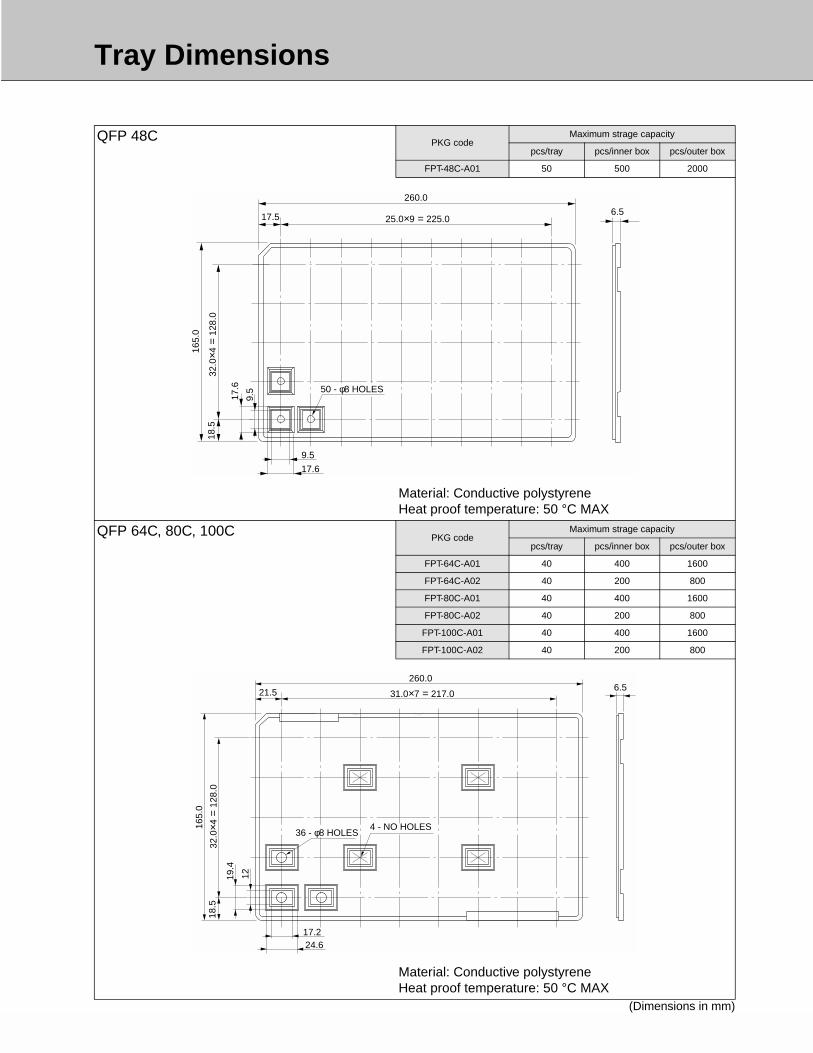
Tray Dimensions
51
QFP 48C PKG codeMaximum strage capacity
pcs/tray pcs/inner box pcs/outer box
FPT-48C-A01 50 500 2000
Material: Conductive polystyreneHeat proof temperature: 50 °C MAX
QFP 64C, 80C, 100C PKG codeMaximum strage capacity
pcs/tray pcs/inner box pcs/outer box
FPT-64C-A01 40 400 1600
FPT-64C-A02 40 200 800
FPT-80C-A01 40 400 1600
FPT-80C-A02 40 200 800
FPT-100C-A01 40 400 1600
FPT-100C-A02 40 200 800
Material: Conductive polystyreneHeat proof temperature: 50 °C MAX
(Dimensions in mm)
260.0
25.0×9 = 225.017.5
165.
0
32.0
×4 =
128
.018
.56.5
17.6
9.5
17.6
9.5
50 - φ8 HOLES
260.0
31.0×7 = 217.021.5
165.
0
32.0
×4 =
128
.018
.5
19.4
12
6.5
24.617.2
36 - φ8 HOLES4 - NO HOLES

Tray Dimensions
52
QFP 68C PKG codeMaximum strage capacity
pcs/tray pcs/inner box pcs/outer box
FPT-68C-A01 40 80 160
FPT-68C-A02 40 80 160
Material: Conductive polystyreneHeat proof temperature: 50 °C MAX
QFP 120C, 160C PKG codeMaximum strage capacity
pcs/tray pcs/inner box pcs/outer box
FPT-120C-A01 15 150 600
FPT-160C-A01 15 150 600
Material: Conductive polystyreneHeat proof temperature: 50 °C MAX
(Dimensions in mm)
260.0
31×7 = 21721.5
165.
0
32×4
= 1
2818
.525
.6
25.6
20
30 - HOLES 10 - NO HOLES
260.0
50.0×4 = 200.030.0
165.
0
52.0
×2 =
104
.030
.5
6.5
23.2
32.823.2
32.8
15 - φ15 HOLES

Tray Dimensions
53
QFP 124C PKG codeMaximum strage capacity
pcs/tray pcs/inner box pcs/outer box
FPT-124C-A03 40 40 160
Material: Conductive polystyreneHeat proof temperature: 50 °C MAX
QFP 164C PKG codeMaximum strage capacity
pcs/tray pcs/inner box pcs/outer box
FPT-164C-A03 24 72 432
FPT-164C-A05 24 72 432
Material: Conductive polystyreneHeat proof temperature: 50 °C MAX
(Dimensions in mm)
260.0
30.4×7 = 212.823.6
165.
0
30.5
×4 =
122
.021
.5
25.0
26.0
26.0
15.3
15.3
10 - NO HOLES
314.96
37.01×7 = 259.0727.94
135.
9
37.0
1×2
= 74
.02
9.6
30.9
4
32.2
32.2

Tray Dimensions
54
QFP 208C PKG codeMaximum strage capacity
pcs/tray pcs/inner box pcs/outer box
FPT-208C-A01 15 15 60
Material: Conductive polystyreneHeat proof temperature: 50 °C MAX
QFP 256C, 320C PKG codeMaximum strage capacity
pcs/tray pcs/inner box pcs/outer box
FPT-256C-A07 15 15 30
FPT-320C-A01 15 15 30
Material: Conductive polystyreneHeat proof temperature: 50 °C MAX
(Dimensions in mm)
260.0
50×4 = 20030
165.
0
52×2
= 1
0430
.535
2524
.8
3524.8
10 - HOLES 5 - NO HOLES
260.0
50×4 = 20030
165.
0
52×2
= 1
0430
.543
25
43
32.25
32.2
5
10 - HOLES 5 - NO HOLES
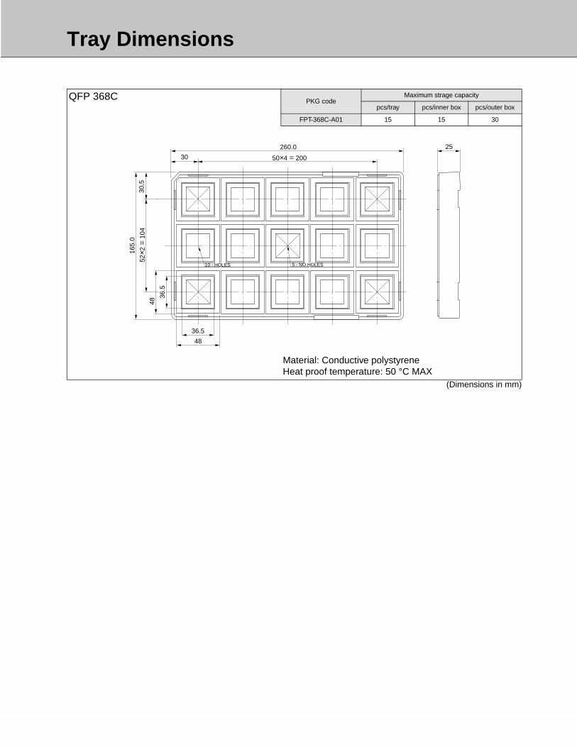
Tray Dimensions
55
QFP 368C PKG codeMaximum strage capacity
pcs/tray pcs/inner box pcs/outer box
FPT-368C-A01 15 15 30
Material: Conductive polystyreneHeat proof temperature: 50 °C MAX
(Dimensions in mm)
260.0
50×4 = 20030
165.
0
52×2
= 1
0430
.5
4825
36.5
48
36.5
10 - HOLES 5 - NO HOLES

Tray Dimensions
56
6.3.6 Ceramic QFP/Cerquad (non-heat proof type)
QFP 120C, 144C, 160C PKG codeMaximum strage capacity
pcs/tray pcs/inner box pcs/outer box
FPT-120C-C01 15 120 240
FPT-144C-C01 15 120 240
FPT-160C-C01 15 120 240
FPT-160C-C04 15 120 240
FPT-160C-C02 15 30 60
Material: Conductive polyphenylenetherHeat proof temperature: 50 °C MAX
QFP 164C PKG codeMaximum strage capacity
pcs/tray pcs/inner box pcs/outer box
FPT-164C-C01 24 72 288
Material: Conductive polyphenylenetherHeat proof temperature: 50 °C MAX
(Dimensions in mm)
260.0
50×4 = 20030
165.
0
52×2
= 1
0430
.534
.5
9.5
28.2
34.528.2
10 - HOLES 5 - NO HOLES
315.0
37.01×7 = 259.0727.94
135.
9
37.0
1×2
= 74
.02
9.6
30.9
4
33.3 25
.78
33.3
25.78
10 - NO HOLES

Tray Dimensions
57
QFP 176C PKG codeMaximum strage capacity
pcs/tray pcs/inner box pcs/outer box
FPT-176C-C01 15 120 240
Material: Conductive polypropyleneHeat proof temperature: 50 °C MAX
QFP 196C PKG codeMaximum strage capacity
pcs/tray pcs/inner box pcs/outer box
FPT-196C-C01 15 120 240
Material: Conductive polyphenylenetherHeat proof temperature: 50 °C MAX
(Dimensions in mm)
260.0
49.8×4 = 199.229.8
165.
0
51.8
×2 =
103
.630
.328
.29.5
23.4
28.2
23.4
10 - HOLES 5 - NO HOLES
260.0
50×4 = 20030
165.
0
52×2
= 1
0430
.533
.8
9.5
45.840.28
28.2
10 - HOLES 5 - NO HOLES

Tray Dimensions
58
QFP 208C PKG codeMaximum strage capacity
pcs/tray pcs/inner box pcs/outer box
FPT-208C-C02 15 120 240
FPT-208C-C03 15 120 240
FPT-208C-C04 15 120 240
Material: Conductive polypropyleneHeat proof temperature: 50 °C MAX
QFP 232C PKG codeMaximum strage capacity
pcs/tray pcs/inner box pcs/outer box
FPT-232C-C01 15 120 240
Material: Conductive polyphenylenetherHeat proof temperature: 50 °C MAX
(Dimensions in mm)
165.
0
52.0
×2 =
104
.030
.533
.3
260.0
50.0×4 = 200.030.09.5
27.4
33.3
27.4
10 - HOLES 5 - NO HOLES
165.
0
52×2
= 1
0430
.545
.4
260.0
50×4 = 200309.5
40.2
8
45.4
40.28
10 - HOLES 5 - NO HOLES

Tray Dimensions
59
QFP 240C PKG codeMaximum strage capacity
pcs/tray pcs/inner box pcs/outer box
FPT-240C-A03 10 30 180
FPT-240C-A05 10 30 180
Material: Conductive polyphenylenetherHeat proof temperature: 50 °C MAX
QFP 240C PKG codeMaximum strage capacity
pcs/tray pcs/inner box pcs/outer box
FPT-240C-C01 15 120 240
Material: Conductive polyphenylenetherHeat proof temperature: 50 °C MAX
(Dimensions in mm)
314.96
62.484×4 = 249.93632.512
135.
89
66.0
4
8.5
34.9
25
41.7
41.7
165.
0
52×2
= 1
0430
.536
.4
36.4
260.0
50×4 = 200309.5
31.4
8
31.48
10 - HOLES 5 - NO HOLES

Tray Dimensions
60
QFP 256C PKG codeMaximum strage capacity
pcs/tray pcs/inner box pcs/outer box
FPT-256C-C01 15 120 240
FPT-256C-C02 15 120 240
FPT-256C-C03 15 30 60
Material: Conductive polyphenylenetherHeat proof temperature: 50 °C MAX
QFP 304C, 368C PKG codeMaximum strage capacity
pcs/tray pcs/inner box pcs/outer box
FPT-304C-C01 15 120 240
FPT-304C-C02 15 120 240
FPT-368C-C01 15 120 240
Material: Conductive polyphenylenetherHeat proof temperature: 50 °C MAX
(Dimensions in mm)
260.0
50×4 = 20030
165.
0
52×2
= 1
0430
.5
32
9.5
44.4
27.4
39.48
10 - HOLES 5 - NO HOLES
165.
0
52×2
= 1
0430
.5
44.4
260.0
50×4 = 200309.5
39.4
8
39.48
44.4
10 - HOLES 5 - NO HOLES

Tray Dimensions
61
LQFP 100C PKG codeMaximum strage capacity
pcs/tray pcs/inner box pcs/outer box
FPT-100C-C01 40 400 1600
Material: Conductive polyvinyl chlorideHeat proof temperature: 50 °C MAX
(Dimensions in mm)
260.0
31.0×7 = 217.021.5
165.
0
32.0
×4 =
128
.06.5
15.6
18.5
15.6

Tray Dimensions
62
6.3.7 Ceramic PGA (non-heat proof type)
PGA 64C PKG codeMaximum strage capacity
pcs/tray pcs/inner box pcs/outer box
PGA-64C-A02 30 30 480
t = 0.5Material: Conductive polyvinyl chlorideHeat proof temperature: 50 °C MAX
PGA 68C PKG codeMaximum strage capacity
pcs/tray pcs/inner box pcs/outer box
PGA-68C-A01 15 30 120
t = 0.5Material: Conductive polyvinyl chloride
Conductive polystyrene (outer tray) Heat proof temperature: 50 °C MAX
(Dimensions in mm)
220.
0260.0 15.0
32.5 39.0×5 = 195.039
.0×4
= 1
56.0
32.0
10.0
25.0
10.0
25.0
245.0
46.5×4 = 186.0
260.0
37.0
165.
0
46.5
×2 =
93.
0
154.
0
14.029.5
36.0
23.0
29.5
14.0

Tray Dimensions
63
PGA 80C, 88C PKG codeMaximum strage capacity
PKG codeMaximum strage capacity
pcs/tray pcs/inner box pcs/outer box pcs/tray pcs/inner box pcs/outer box
PGA-80C-A01 20 20 320 PGA-88C-A06 20 20 320
PGA-88C-A05 20 20 320
t = 0.5Material: Conductive polyvinyl chlorideHeat proof temperature: 50 °C MAX
PGA 88C, 107C PKG codeMaximum strage capacity
PKG codeMaximum strage capacity
pcs/tray pcs/inner box pcs/outer box pcs/tray pcs/inner box pcs/outer box
PGA-88C-A01 20 20 320 PGA-107C-A01 20 20 320
PGA-88C-A02 20 20 320 PGA-107C-A02 20 20 320
t = 0.5Material: Conductive polyvinyl chlorideHeat proof temperature: 50 °C MAX
(Dimensions in mm)
259.0
33.2538.5×5 = 192.5
219.
0
38.5
×4 =
154
.032
.5
7.0
7.0
31.0
16.0
31.0
259.0 15.0
40.5 44.5×4 = 178.0
219.
0
44.5
×3 =
133
.542
.75
8.0
8.0
31.5
31.5

Tray Dimensions
64
PGA 121C (with fins)
PKG codeMaximum strage capacity
PKG codeMaximum strage capacity
pcs/tray pcs/inner box pcs/outer box pcs/tray pcs/inner box pcs/outer box
PGA-121C-A01 15 30 120 PGA-121C-A02 15 30 120
t = 0.5Material: Conductive polyvinyl chloride
Conductive polystyrene (outer tray) Heat proof temperature: 50 °C MAX
PGA 135C PKG codeMaximum strage capacity
PKG codeMaximum strage capacity
pcs/tray pcs/inner box pcs/outer box pcs/tray pcs/inner box pcs/outer box
PGA-135C-C02 20 20 320 PGA-135C-A02 20 20 320
PGA-135C-A01 20 20 320 PGA-135C-A06 20 20 320
t = 0.5Material: Conductive polyvinyl chlorideHeat proof temperature: 50 °C MAX
(Dimensions in mm)
245.0
46.5×4 = 186.0
260.0
37.0
165.
0
46.5
×2 =
93.
0
154.
0
34.0
36.0
23.0
12.0
34.0
12.0
259.0 13.0
36.5 46.5×4 = 186.0
219.
0
46.5
×3 =
139
.539
.75
36.5
36.5
12.0
12.0
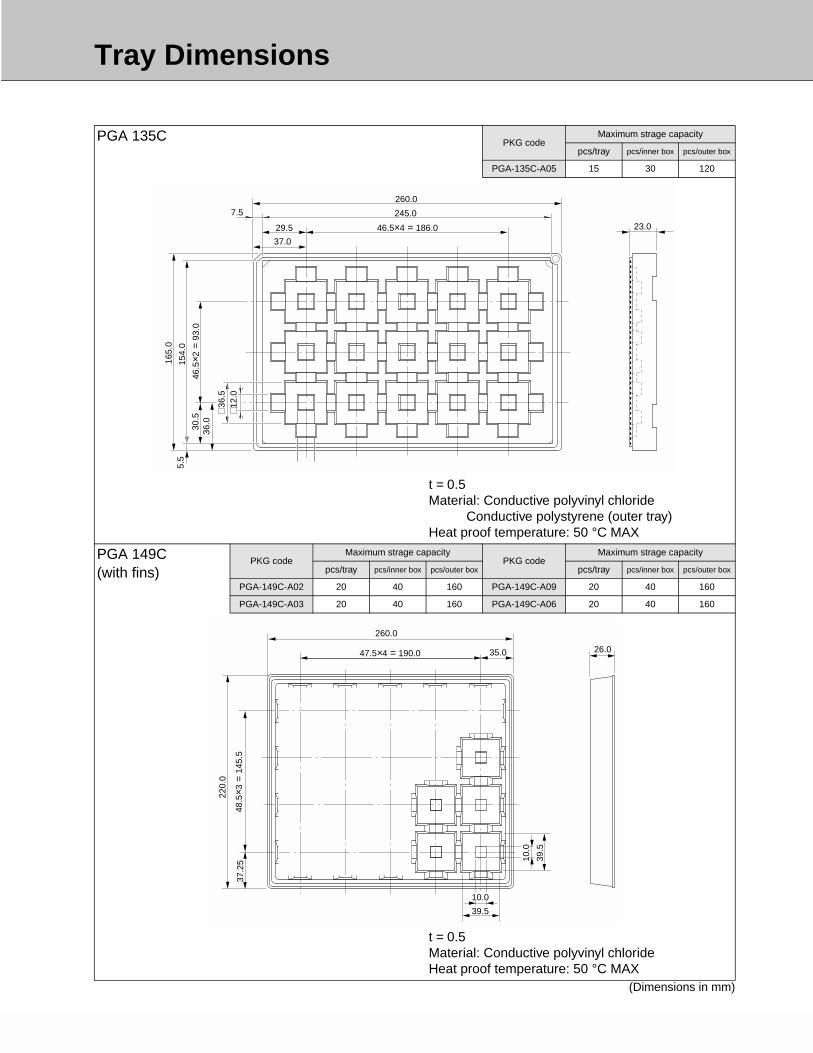
Tray Dimensions
65
PGA 135C PKG codeMaximum strage capacity
pcs/tray pcs/inner box pcs/outer box
PGA-135C-A05 15 30 120
t = 0.5Material: Conductive polyvinyl chloride
Conductive polystyrene (outer tray) Heat proof temperature: 50 °C MAX
PGA 149C(with fins)
PKG codeMaximum strage capacity
PKG codeMaximum strage capacity
pcs/tray pcs/inner box pcs/outer box pcs/tray pcs/inner box pcs/outer box
PGA-149C-A02 20 40 160 PGA-149C-A09 20 40 160
PGA-149C-A03 20 40 160 PGA-149C-A06 20 40 160
t = 0.5Material: Conductive polyvinyl chlorideHeat proof temperature: 50 °C MAX
(Dimensions in mm)
245.0
46.5×4 = 186.0
260.0
29.5
37.0
165.
0
46.5
×2 =
93.
0
154.
0
30.5
36.0
23.036
.512
.0
5.5
7.5
260.0
35.047.5×4 = 190.0
220.
0
48.5
×3 =
145
.537
.25 39
.5
10.0
39.5
10.0
26.0

Tray Dimensions
66
PGA 179C PKG codeMaximum strage capacity
pcs/tray pcs/inner box pcs/outer box
PGA-179C-A02 20 20 320
PGA-179C-A03 20 20 320
t = 0.5Material: Conductive polyvinyl chlorideHeat proof temperature: 50 °C MAX
PGA 179C (with fins) , 401C PKG codeMaximum strage capacity
pcs/tray pcs/inner box pcs/outer box
PGA-179C-A06 15 30 120
PGA-401C-A04 15 30 120
t = 0.5Material: Conductive polyvinyl chloride
Conductive polystyrene (outer tray) Heat proof temperature: 50 °C MAX
(Dimensions in mm)
260.0 15.0
35.0 47.5×4 = 190.022
0.0
48.5
×3 =
145
.537
.25
39.514
.0
14.0
39.5
245.0
46.5×4 = 186.0
260.0
37.0
165.
0
46.5
×2 =
93.
0
154.
0
41.5
36.0
23.0
14.0
41.5
14.0

Tray Dimensions
67
PGA 208CPKG code
Maximum strage capacityPKG code
Maximum strage capacity
pcs/tray pcs/inner box pcs/outer box pcs/tray pcs/inner box pcs/outer box
PGA-208C-A02 12 12 192 PGA-211C-A01 12 12 192
t = 0.5Material: Conductive polyvinyl chlorideHeat proof temperature: 50 °C MAX
PGA 179C, 208C (with fins)
PKG codeMaximum strage capacity
PKG codeMaximum strage capacity
pcs/tray pcs/inner box pcs/outer box pcs/tray pcs/inner box pcs/outer box
PGA-179C-A04 12 24 96 PGA-208C-A05 12 24 96
PGA-208C-A03 12 24 96 PGA-208C-A06 12 24 96
PGA-208C-A04 12 24 96 PGA-208C-A07 12 24 96
t = 1.0Material: Conductive polyvinyl chlorideHeat proof temperature: 50 °C MAX
(Dimensions in mm)
259.0
44.057.0×3 = 171.021
9.0
57.0
×2 =
114
.052
.5
44.0
14.0
44.0
14.0
14.0
260.0
44.557.0×3 = 171.0
220.
0
57.0
×2 =
114
.053
.0
44.5
30.0
44.5
14.0
14.0

Tray Dimensions
68
50mil PGA 256C PKG codeMaximum strage capacity
pcs/tray pcs/inner box pcs/outer box
PGA-256C-A01 21 21 336
t = 0.5Material: Conductive polyvinyl chlorideHeat proof temperature: 50 °C MAX
100mil PGA 256C PKG codeMaximum strage capacity
pcs/tray pcs/inner box pcs/outer box
PGA-256C-A02 8 8 64
PGA-256C-A03 8 8 64
PGA-256C-A04 8 8 64
PGA-256C-A05 8 8 64
PGA-256C-A07 8 8 64
t = 0.5Material: Conductive polyvinyl chlorideHeat proof temperature: 50 °C MAX
(Dimensions in mm)
230.3 9.0
22.15 31.0×6 = 186.0
125.
3
28.6
534
.0×2
= 6
8.0
9.0
27.4
9.0
27.4
230.3 14.0
32.65 55.0×3 = 165.0
125.
3
35.1
555
.0
49.0
49.0
20
20
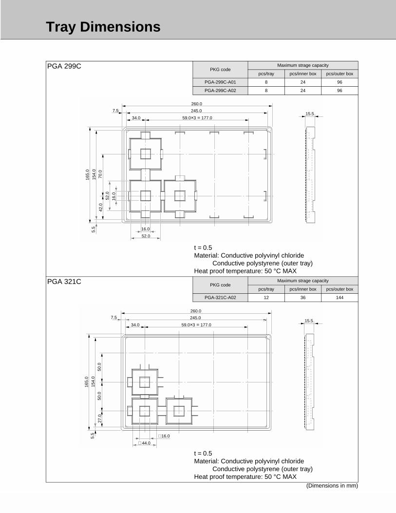
Tray Dimensions
69
PGA 299C PKG codeMaximum strage capacity
pcs/tray pcs/inner box pcs/outer box
PGA-299C-A01 8 24 96
PGA-299C-A02 8 24 96
t = 0.5Material: Conductive polyvinyl chloride
Conductive polystyrene (outer tray) Heat proof temperature: 50 °C MAX
PGA 321C PKG codeMaximum strage capacity
pcs/tray pcs/inner box pcs/outer box
PGA-321C-A02 12 36 144
t = 0.5Material: Conductive polyvinyl chloride
Conductive polystyrene (outer tray) Heat proof temperature: 50 °C MAX
(Dimensions in mm)
245.0
59.0×3 = 177.0
260.0
34.0
165.
0
154.
0
52.0
42.0
15.5
16.0
70.0
52.0
16.0
7.5
5.5
245.0
59.0×3 = 177.034.0
44.0
27.0
15.5
16.0
50.0
50.0
260.0
165.
0
154.
05.
5
7.5

Tray Dimensions
70
PGA 361C PKG codeMaximum strage capacity
pcs/tray pcs/inner box pcs/outer box
PGA-361C-A01 8 24 96
t = 0.5Material: Conductive polyvinyl chloride
Conductive polystyrene (outer tray) Heat proof temperature: 50 °C MAX
PGA 401C PKG codeMaximum strage capacity
pcs/tray pcs/inner box pcs/outer box
PGA-401C-A02 8 24 96
t = 0.5Material: Conductive polyvinyl chloride
Conductive polystyrene (outer tray) Heat proof temperature: 50 °C MAX
(Dimensions in mm)
7042
154
47.0
15.5245.0
59.0×3 = 177.034.0
260.0
7.516
.0
5.5
165.
0
7042
5.5
165.
0
154
49.0
245.0
59.0×3 = 177.034.0
260.0
7.5 15.5
16.0

Tray Dimensions
71
PGA 441C (with fins) PKG codeMaximum strage capacity
pcs/tray pcs/inner box pcs/outer box
PGA-441C-A01 12 24 96
PGA-441C-A03 12 24 96
t = 1.0Material: Conductive polyvinyl chloride
Conductive polystyrene (outer tray) Heat proof temperature: 50 °C MAX
PGA 441C PKG codeMaximum strage capacity
pcs/tray pcs/inner box pcs/outer box
PGA-441C-A06 12 36 144
t = 1.0Material: Conductive polyvinyl chloride
Conductive polystyrene (outer tray) Heat proof temperature: 50 °C MAX
(Dimensions in mm)
245.0
59.0×3 = 177.0
260.0
34.0
7.5
165.
0
154.
05.
527
.0
23.0
50×2
= 1
00.0
36.0
18.0
245.07.5
59.0×3 = 177.0
260.0
34.0
165.
0
154.
05.
527
.0
15.5
50×2
= 1
00.0
36.0
18.0

Tray Dimensions
72
6.3.8 Module (non-heat proof type)
MODULE PKG codeMaximum strage capacity
pcs/tray pcs/inner box pcs/outer box
MSS-72P-P11 40 80 320
MSS-72P-P23 40 80 320
MSS-72P-P24 40 80 320
MSS-72P-P27 40 80 320
MSS-72P-P29 40 80 320
MSS-72P-P39 40 80 320
MSS-72P-P48 40 80 320
MSS-72P-P49 40 80 320
t = 0.9Material: Conductive polystyreneHeat proof temperature: 50 °C MAX
(Dimensions in mm)
85.3 61
21
40
1
20
97.5
108.8
292.6
280.
5
2
15
218.
50 =
19×
11.5
31
0.9
18.0
33

Tray Dimensions
73
MODULE PKG codeMaximum strage capacity
PKG codeMaximum strage capacity
pcs/tray pcs/inner box pcs/outer box pcs/tray pcs/inner box pcs/outer box
MDS-168P-P04 20 20 80 MDS-168P-P20 20 20 80
MDS-168P-P05 20 20 80 MDS-168P-P21 20 20 80
MDS-168P-P06 20 20 80 MDS-168P-P22 20 20 80
MDS-168P-P07 20 20 80 MDS-168P-P23 20 20 80
MDS-168P-P08 20 20 80 MDS-168P-P24 20 20 80
MDS-168P-P09 20 20 80 MDS-168P-P25 20 20 80
MDS-168P-P10 20 20 80 MDS-168P-P26 20 20 80
MDS-168P-P11 20 20 80 MDS-168P-P27 20 20 80
MDS-168P-P12 20 20 80 MDS-168P-P36 20 20 80
MDS-168P-P13 20 20 80 MDS-168P-P37 20 20 80
MDS-168P-P14 20 20 80 MDS-168P-P38 20 20 80
MDS-168P-P16 20 20 80 MDS-168P-P39 20 20 80
MDS-168P-P17 20 20 80 MDS-168P-P40 20 20 80
MDS-168P-P18 20 20 80 MDS-168P-P41 20 20 80
MDS-168P-P19 20 20 80
t = 1.0Material: Conductive polystyreneHeat proof temperature: 50 °C MAX
(Dimensions in mm)
292.6
280.
9
1
20
C13
280.
9
P10
×19
= 19
0(7
.75)
44.645.6
1
2.324.218.1
1.5

Tray Dimensions
74
6.3.9 BGA, T-BGA, FBGA (heat proof type)
BGA 256, T-BGA 256
PKG codeMaximum strage capacity
PKG codeMaximum strage capacity
pcs/tray pcs/inner box pcs/outer box pcs/tray pcs/inner box pcs/outer box
BGA-256P-M01 40 400 2400 BGA-256P-M04 40 400 2400
BGA-256P-M02 40 400 2400
Material: Conductive polyphenylenetherHeat proof temperature: 125 °C MAX
BGA 352, 420, 560 PKG codeMaximum strage capacity
PKG codeMaximum strage capacity
pcs/tray pcs/inner box pcs/outer box pcs/tray pcs/inner box pcs/outer box
BGA-352P-M01 24 120 720 BGA-420P-M01 24 240 1440
BGA-352P-M02 24 240 1440 BGA-420P-M02 24 240 1440
BGA-352P-M03 24 240 1440 BGA-420P-M03 24 120 720
BGA-352P-M04 24 120 720 BGA-560P-M01 24 240 1440
BGA-352P-M05 24 120 720
Material: Conductive polyphenylenetherHeat proof temperature: 125 °C MAX
(Dimensions in mm)
135.
9
29.2
×3 =
87.
624
.15
27.1
27.1
7.6226.1 29.2×9 = 262.8
315
322.6
6-NO HOLES
38.0
×2 =
76.
029
.95
35.15
35.1
5
38.0×7 = 266.024.50
315.0
4-NO HOLES
7.62
322.6
135.
9
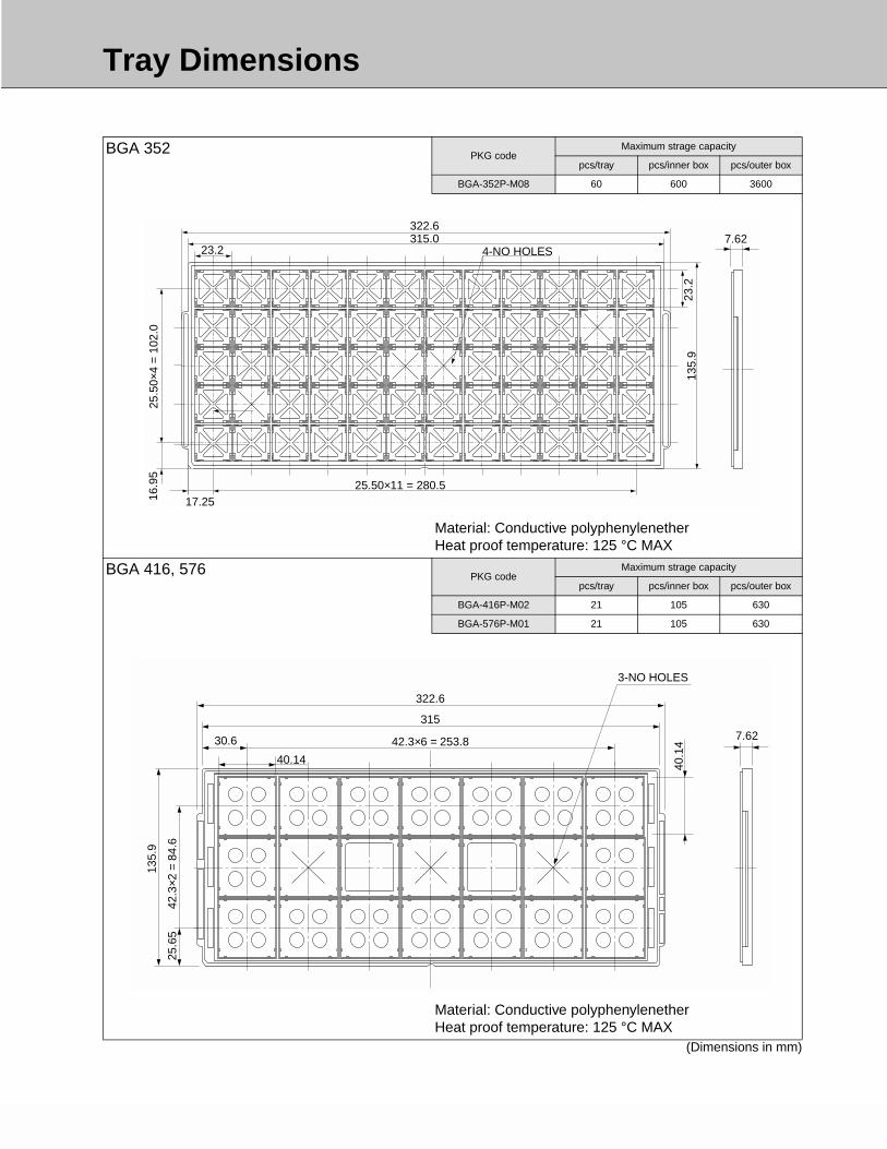
Tray Dimensions
75
BGA 352 PKG codeMaximum strage capacity
pcs/tray pcs/inner box pcs/outer box
BGA-352P-M08 60 600 3600
Material: Conductive polyphenylenetherHeat proof temperature: 125 °C MAX
BGA 416, 576 PKG codeMaximum strage capacity
pcs/tray pcs/inner box pcs/outer box
BGA-416P-M02 21 105 630
BGA-576P-M01 21 105 630
Material: Conductive polyphenylenetherHeat proof temperature: 125 °C MAX
(Dimensions in mm)
322.6
17.25
23.2
25.50×11 = 280.5
315.0
25.5
0×4
= 1
02.0
135.
923
.2
16.9
5
4-NO HOLES7.62
40.14
40.1
4
25.6
542
.3×2
= 8
4.6
135.
9
42.3×6 = 253.8
3157.62
322.6
30.6
3-NO HOLES

Tray Dimensions
76
BGA 672 PKG codeMaximum strage capacity
pcs/tray pcs/inner box pcs/outer box
BGA-672P-M01 12 60 360
Material: Conductive polyphenylenetherHeat proof temperature: 125 °C MAX
T-BGA 272 PKG codeMaximum strage capacity
pcs/tray pcs/inner box pcs/outer box
BGA-272P-M01 36 360 2160
Material: Conductive polyphenylenetherHeat proof temperature: 125 °C MAX
(Dimensions in mm)
30
3075
.913
5.9
51.0×5 = 255.0315
322.6
7.62
45.2
45.2 6-NO HOLES
135.
9
31.4
×3 =
94.
220
.85
7.62
31.1 31.6×8 = 252.8
315.0
322.6
4-NO HOLES29.25
8-20×7 HOLES
29.2
5
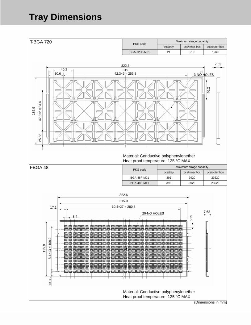
Tray Dimensions
77
T-BGA 720 PKG codeMaximum strage capacity
pcs/tray pcs/inner box pcs/outer box
BGA-720P-M01 21 210 1260
Material: Conductive polyphenylenetherHeat proof temperature: 125 °C MAX
FBGA 48 PKG codeMaximum strage capacity
pcs/tray pcs/inner box pcs/outer box
BGA-48P-M01 392 3920 23520
BGA-48P-M11 392 3920 23520
Material: Conductive polyphenylenetherHeat proof temperature: 125 °C MAX
(Dimensions in mm)
30.640.2
42.3×6 = 253.8315
322.6
40.2
7.62
3-NO HOLES
135.
9
42.3
×2 =
84.
625
.65
7.6217.1 10.4×27 = 280.8
315.0
322.6
135.
9
13.3
58.
4×13
= 1
09.2
8.4
6.35
20-NO HOLES
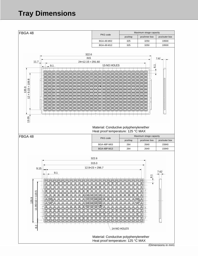
Tray Dimensions
78
FBGA 48 PKG codeMaximum strage capacity
pcs/tray pcs/inner box pcs/outer box
BGA-48-M02 325 3250 19500
BGA-48-M12 325 3250 19500
Material: Conductive polyphenylenetherHeat proof temperature: 125 °C MAX
FBGA 48 PKG codeMaximum strage capacity
pcs/tray pcs/inner box pcs/outer box
BGA-48P-M03 264 2640 15840
BGA-48P-M13 264 2640 15840
Material: Conductive polyphenylenetherHeat proof temperature: 125 °C MAX
(Dimensions in mm)
315
13-NO HOLES24×12.15 = 291.60
135.
912
× 9
.15
= 10
9.8
11.7
13.0
5
7.62
322.6
9.1 6.1
7.629.15 12.9×23 = 296.7
315.0
322.6
135.
9
8.2
11.9
5×10
= 1
19.5
9.1
8.1
14-NO HOLES

Tray Dimensions
79
FBGA 57 PKG codeMaximum strage capacity
pcs/tray pcs/inner box pcs/outer box
BGA-57P-M01 187 1870 11220
Material: Conductive polyphenylenetherHeat proof temperature: 125 °C MAX
FBGA 61 PKG codeMaximum strage capacity
pcs/tray pcs/inner box pcs/outer box
BGA-61P-M02 240 2400 14400
Material: Conductive polyphenylenetherHeat proof temperature: 125 °C MAX
(Dimensions in mm)
7.62
11.50 16×18.25 = 292.0
315.0
322.6
135.
9
8.2
10×1
1.95
= 1
19.5
14.25 8.25
11-NO HOLES
9.15
135.
9
9×13
.10
= 11
7.9
9.00
9.15
322.6
315.0
23×12.9 = 296.79.15
20-NO HOLES

Tray Dimensions
80
FBGA 69 PKG codeMaximum strage capacity
pcs/tray pcs/inner box pcs/outer box
BGA-69P-M02 220 2200 13200
Material: Conductive polyphenylenetherHeat proof temperature: 125 °C MAX
FBGA 77 PKG codeMaximum strage capacity
pcs/tray pcs/inner box pcs/outer box
BGA-77P-M01 170 1700 10200
Material: Conductive polyphenylenetherHeat proof temperature: 125 °C MAX
(Dimensions in mm)
11.15
322.6315
19×15.50 = 294.5
135.
910
×11.
95 =
119
.5.2
0
10.25
8-NO HOLES
8.33
7.62
7.62
11.50 16×18.25 = 292
315
322.6
135.
9
9.00
9×13
.1 =
117
.9
14.15 9.15
16-NO HOLES

Tray Dimensions
81
FBGA 112 PKG codeMaximum strage capacity
pcs/tray pcs/inner box pcs/outer box
BGA-112P-M01 198 1980 11880
Material: Conductive polyphenylenetherHeat proof temperature: 125 °C MAX
FBGA 120, 144, 168, 176
PKG codeMaximum strage capacity
PKG codeMaximum strage capacity
pcs/tray pcs/inner box pcs/outer box pcs/tray pcs/inner box pcs/outer box
BGA-120P-M01 152 1520 9120 BGA-168P-M01 152 1520 9120
BGA-144P-M01 152 1520 9120 BGA-176P-M02 152 1520 9120
BGA-144P-M02 152 1520 9120
Material: Conductive polyphenylenetherHeat proof temperature: 125 °C MAX
(Dimensions in mm)
7.629.45 14.1×21 = 296.1
315.0
322.6
135.
9
9.55
14.6
×8 =
116
.8
10.15
10.1
5
8-NO HOLES
7.6210.8 16.3×18 = 293.4
315.0
322.6
135.
9
10.5
516
.4×7
= 1
14.8
8-NO-HOLES12.15
12.1
5

Tray Dimensions
82
FBGA 192 PKG codeMaximum strage capacity
pcs/tray pcs/inner box pcs/outer box
BGA-192P-M01 119 1190 7140
Material: Conductive polyphenylenetherHeat proof temperature: 125 °C MAX
FBGA 192 PKG codeMaximum strage capacity
pcs/tray pcs/inner box pcs/outer box
BGA-192P-M02 198 1980 11880
Material: Conductive polyphenylenetherHeat proof temperature: 125 °C MAX
(Dimensions in mm)
7.6211.5 18.25×16 = 292.0
315.0
322.6
135.
9
11.7
18.7
5×6
= 11
2.5
14.2
14.2
11-NO HOLES
7.62
10.2
9.45 21×14.1 = 296.1
315
322.6
135.
9
9.55
8×14
.6 =
116
.8
10.2

Tray Dimensions
83
FBGA 224 PKG codeMaximum strage capacity
pcs/tray pcs/inner box pcs/outer box
BGA-224P-M03 112 1120 6720
Material: Conductive polyphenylenetherHeat proof temperature: 125 °C MAX
FBGA 240 PKG codeMaximum strage capacity
pcs/tray pcs/inner box pcs/outer box
BGA-240P-M01 198 1980 11880
Material: Conductive polyphenylenetherHeat proof temperature: 125 °C MAX
(Dimensions in mm)
7.6219.50 18.4×15 = 276.0
315.0
322.6
135.
9
12.7
518
.4×6
= 1
10.4
8-NO-HOLES
16.23
16.2
3
7.62
9.45 21×14.1 = 296.1
315
322.6
135.
9
9.55
8×14
.6 =
116
.8
10.2 10.2

Tray Dimensions
84
FBGA 288, 320 PKG codeMaximum strage capacity
pcs/tray pcs/inner box pcs/outer box
BGA-288P-M02 90 900 5400
BGA-320P-M01 90 900 5400
Material: Conductive polyphenylenetherHeat proof temperature: 125 °C MAX
(Dimensions in mm)
7.6214.70 20.4 × 14 = 285.6
315.0
322.6
135.
9
16.9
520
.4~
5 =
102.
0
8-NO-HOLES18.20
18.2
0
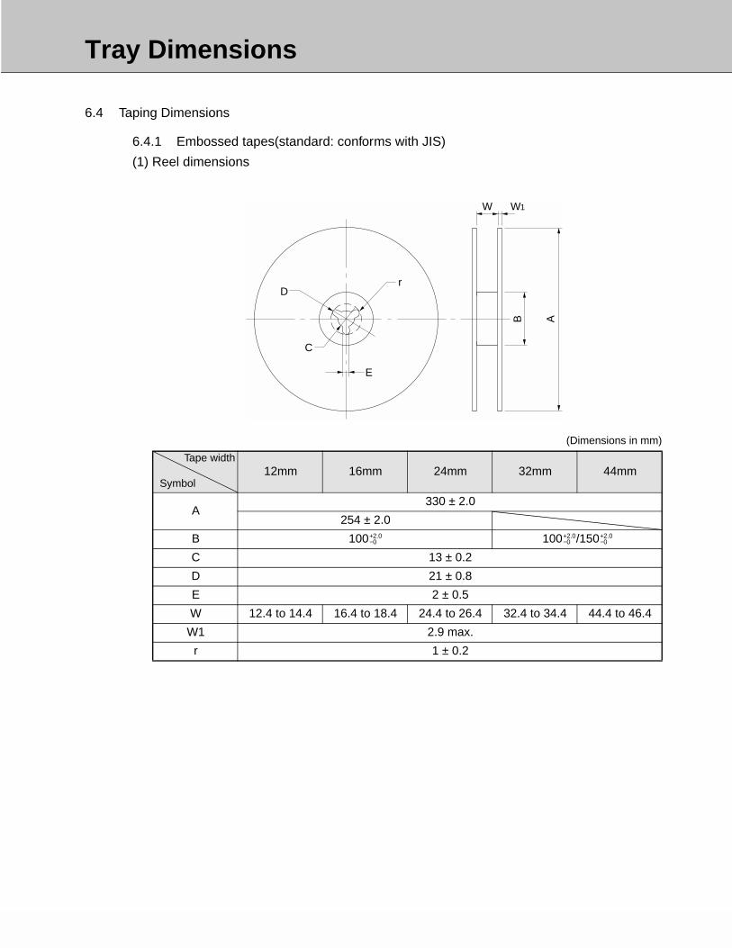
Tray Dimensions
85
6.4 Taping Dimensions
6.4.1 Embossed tapes(standard: conforms with JIS)
(1) Reel dimensions
E
C
Dr
W W1
B A
(Dimensions in mm)
Tape width
Symbol12mm 16mm 24mm 32mm 44mm
A330 ± 2.0
254 ± 2.0
B 100 100 /150
C 13 ± 0.2
D 21 ± 0.8
E 2 ± 0.5
W 12.4 to 14.4 16.4 to 18.4 24.4 to 26.4 32.4 to 34.4 44.4 to 46.4
W1 2.9 max.
r 1 ± 0.2
+2.0−0
+2.0−0
+2.0−0

Tray Dimensions
86
(2) IC orientation
a) SOP, QFP, SOJ, SON, BCC, FBGA
• EF type
• ER type
b) LCC, QFJ, TSOP
• EF type
• ER type
User Direction of Feed
User Direction of Feed (Reel side) Pin 1
User Direction of Feed (Reel side)
Pin 1
User Direction of Feed (Reel side) Pin 1
User Direction of Feed (Reel side)
Pin 1

Tray Dimensions
87
(3) Tape dimensions
12mm, 16mm, 24mm tape width
32mm, 44mm tape width
1.55± 0.05
1.75
±0.
10F
W
PA
2.0
± 0.1TT1
0.3
B
± 0.1
± 0.05 4.0
±0.
1
± 0.1
±0.
3
±0.
1
± 0.1
± 0.1
D min∗
*: The pocket shapes have raised bottoms, except for BCCs.
1.55 ± 0.05
1.75
±0.
10F
W
PA
2.0
± 0.1TT1
0.3
B
± 0.1
± 0.05 4.0
±0.
1
± 0.1
±0.
3
±0.
1
± 0.1
± 0.1
D min
1.75

Tray Dimensions
88
• Tape dimansions(Dimensions in mm)
PKG codeSymbol
A B F P T T1 D W
SOP
FPT-8P-M01 8.3 6.65 7.5 12.0 2.85 2.35 2.0 16.0
FPT-8P-M02 6.5 5.4 5.5 8.0 2.1 1.7 2.0 12.0
FPT-14P-M04 8.5 10.6 7.5 12.0 2.5 2.2 2.0 16.0
FPT-16P-M03 10.85 13.0 11.5 12.0 3.55 3.05 2.0 24.0
FPT-16P-M04 6.9 10.5 7.5 12.0 2.45 1.95 1.5 16.0
FPT-16P-M06 8.5 10.6 7.5 12.0 2.5 2.2 2.0 16.0
FPT-20P-M01 8.2 13.1 11.5 12.0 2.7 2.3 2.0 24.0
FPT-20P-M02 10.85 13.0 11.5 12.0 3.55 3.05 2.0 24.0
FPT-20P-M05 10.85 13.0 11.5 12.0 3.55 3.05 2.0 24.0
FPT-24P-M01 8.5 15.6 11.5 12.0 2.8 2.2 2.0 24.0
FPT-24P-M02 10.65 15.6 11.5 12.0 3.3 2.8 2.0 24.0
FPT-28P-M01 10.8 18.2 11.5 16.0 3.3 2.8 2.0 24.0
FPT-32P-M03 14.8 21.1 14.2 16.0 3.1 2.6 2.0 32.0
SSOP
FPT-8P-M03 6.7 3.9 5.5 8.0 1.85 1.35 1.5 12.0
FPT-16P-M05 6.9 5.5 7.5 12.0 2.0 1.5 1.6 16.0
FPT-20P-M03 6.9 7.0 7.5 12.0 2.0 1.5 1.5 16.0
FPT-20P-M04 6.9 7.0 7.5 12.0 2.0 1.5 1.5 16.0
FPT-24P-M03 8.1 8.3 7.5 12.0 2.0 1.5 1.6 16.0
FPT-30P-M02 8.1 10.2 7.5 12.0 2.0 1.5 1.6 16.0
FPT-34P-M01 10.8 18.2 11.5 16.0 3.3 2.8 2.0 24.0
FPT-34P-M02 10.8 18.2 11.5 16.0 3.3 2.8 2.0 24.0
FPT-34P-M03 8.55 11.5 11.5 12.0 1.8 1.35 2.0 24.0
FPT-40P-M01 12.4 18.2 11.5 16.0 3.3 2.8 2.0 24.0
TSOP
FPT-32P-M24 8.5 20.4 14.2 12.0 1.65 1.25 2.0 32.0
FPT-32P-M25 8.5 20.4 14.2 12.0 1.65 1.25 2.0 32.0
FPT-40P-M06 10.35 20.4 14.2 16.0 1.7 1.4 2.1 32.0
FPT-40P-M07 10.35 20.4 14.2 16.0 1.7 1.4 2.1 32.0
FPT-44P-M07 12.15 18.95 11.5 16.0 1.65 1.25 2.0 24.0
FPT-44P-M08 12.15 18.95 11.5 16.0 1.65 1.25 2.0 24.0
FPT-44P-M16 16.6 28.8 20.2 24.0 3.5 3.0 2.0 44.0
FPT-44P-M18 12.15 18.95 11.5 16.0 1.65 1.25 2.0 24.0
FPT-48P-M19 12.6 20.4 14.2 16.0 1.6 1.2 2.0 32.0
FPT-48P-M20 12.6 20.4 14.2 16.0 1.6 1.2 2.0 32.0
FPT-50P-M05 12.25 21.35 14.2 16.0 1.7 1.2 2.0 32.0
FPT-50P-M06 12.25 21.35 14.2 16.0 1.7 1.2 2.0 32.0

Tray Dimensions
89
SON
LCC-40P-M02 10.35 11.2 11.5 12.0 1.25 0.95 2.0 24.0
LCC-46P-M02 10.45 12.55 11.5 12.0 1.35 0.95 2.0 24.0
BCC
LCC-16P-M02 3.65 4.8 5.5 8.0 1.0 1.5 12.0
LCC-16P-M03 4.45 4.8 5.5 8.0 1.0 1.5 12.0
LCC-48P-M02 7.25 7.25 5.50 12.0 1.0 1.5 12.0
QFP FPT-32P-M21 9.5 9.5 7.5 12.0 2.2 1.7 1.6 16.0
LQFP
FPT-48P-M05 9.5 9.5 7.5 12.0 2.2 1.7 1.6 16.0
FPT-64P-M03 12.5 12.5 11.5 16.0 2.2 1.7 2.0 24.0
QFJ
LCC-28P-M03 12.85 12.85 11.5 16.0 4.8 3.7 2.0 24.0
LCC-32P-M02 12.8 15.3 11.5 16.0 4.0 2.8 1.9 24.0
LCC-44P-M02 17.9 17.9 14.2 20.0 4.8 3.7 2.0 32.0
LCC-68P-M02 25.6 25.6 20.2 32.0 4.8 3.7 2.0 44.0
LCC-84P-M02 30.7 30.7 20.2 36.0 4.8 3.7 2.0 44.0
SOJ
LCC-28C-A04 11.95 18.95 11.5 16.0 4.45 2.8 2.0 24.0
LCC-42P-M01 11.6 27.75 20.2 16.0 4.1 2.9 1.5 44.0
FBGA
BGA-48P-M01 6.3 8.3 7.5 8.0 1.85 0.85 1.5 16.0
BGA-48P-M02 6.1 9.1 7.5 8.0 1.85 0.85 1.5 16.0
BGA-48P-M03 8.1 9.25 11.5 12.0 1.26 0.72 1.5 24.0
(Dimensions in mm)
PKG codeSymbol
A B F P T T1 D W

Tray Dimensions
90
6.5 Dimensions for Containers
(1) Dimensions for inner box
• TypeA
• TypeB
• TypeC
• TypeD
• TypeE
L W
H
L
W
H
L
W
H
L
W
H
L
W
H

Tray Dimensions
91
(2) Dimensions for outer box
Inner type
Dimensions for inner box
L W H
Tube A 550 125 75
Tray Dimensions 165.00 × 260.00 B 180 275 45
135.90 × 322.60 B 165 360 75
135.90 × 314.96
135.90 × 315.00
135.89 × 314.96
220.00 × 260.00 C 225 265 15
219.00 × 259.00
292.00 × 280.50 D 320 290 65
Emboss Reel φ330 Tape width 12.16 D 365 345 40
24.32 365 345 50
44 365 345 65
φ254 E 265 265 50
(Dimensions in mm)
Dimensions for outer box
L W H
Tube 580 305 210
Tray Dimensions 165.00 × 260.00 395 315 215
135.90 × 322.60 580 395 210
135.90 × 314.96
135.90 × 315.00
135.89 × 314.96
220.00 × 260.00 580 305 210
219.00 × 259.00
292.00 × 280.50 340 320 295
Emboss Reel φ330 Tape width 12.16 425 410 325
24.32
44
φ254 580 305 210
(Dimensions in mm)
L
W
H
Related Documents