Predictive Compact Modeling of Abnormal LDMOS Characteristics Due to Overlap-Length Modification Takahiro Iizuka HiSIM Research Center Hiroshima University Higashi-Hiroshima, Japan [email protected] Hidenori Kikuchihara HiSIM Research Center Hiroshima University Higashi-Hiroshima, Japan [email protected] Dondee Navarro HiSIM Research Center Hiroshima University Higashi-Hiroshima, Japan [email protected] Hans Jürgen Mattausch HiSIM Research Center Hiroshima University Higashi-Hiroshima, Japan [email protected] Mitiko Miura-Mattausch HiSIM Research Center Hiroshima University Higashi-Hiroshima, Japan [email protected] Daniel Nestor Rus Allegro MicroSystems, LLC, Buenos Aires, Argentina [email protected] Abstract—Further compact-model development for LDMOS is reported, enabling concurrent device and circuit optimizations by only varying the ratio between gate-overlap length (Lover) and resistive-drift length (Ldrift). Different from the conventional carrier-dynamics understanding within these two regions, LDMOS shows abnormal characteristics during such a ratio variation. The pinch-off condition occurs under the gate overlap region, and the pinch-off point is found to move along Lover with increased drain voltage, even under the accumulation condition. This means that carrier conductivity is no longer controlled by the gate voltage but by the drain voltage. The precise pinch-off condition is determined by the field balancing within gate-overlap and resistive-drift regions. The pinch-off length (ΔL) within Lover sustains Vds together with Ldrift. Thus, the pinch-off region contributes as a part of Ldrift and improves the device’s high-voltage applicability. A new model is developed to describe this balancing phenomenon analytically, where the key physical quantity is ΔL. The developed ΔL model considers the potential distribution along Lover together with Ldrift. At the pinch-off point, the field induced by Vgs and that by Vds are assumed to be equal, which derives an analytical description for ΔL. Evaluation results with the developed model are verified with 2D-numerical-device-simulation results. Keywords—power MOSFETs, LDMOS, compact model, overlap length, conductivity modulation I. INTRODUCTION LDMOS (lateral double-diffused MOS) [1] is widely used for power applications. A schematic LDMOS structure is depicted in Fig. 1a. It can be seen that the device consists of an intrinsic MOSFET and a long lightly- doped drift region with the length of Ldrift, where most of the applied voltage is sustained. Additionally, the gate-overlap length, Lover, is relatively long, which controls the carrier flow together with the channel region. Geometrical dependence with Lover and Ldrift varied were studied [2], [3]. This geometrical freedom would lead to an optimization of LDMOS for different voltage-rating, through varying the ratio of the conductive Lover and the resistive Ldrift. For this device technology to be truly usable in actual circuit designing, a good compact model equipped with geometrical scaling capabilities is helpful. Measured Ids- Vgs characteristics are shown in Fig. 1b, where Ldrift is fixed to 0.4μm and Lover is varied from short to extremely long length. Though the measurements show conventional features for low Vds for all lengths Lover, the I- V characteristics, especially in case of gm, show no clear tendency as a function of Lover. Current-driving capability is kept high for relatively short Lover, which, however, reduces drastically for long Lover. II. ANALYSIS OF OBSERVED PHENOMENON Simulation experiments using 2D device simulator [4] were undertaken to analyze the measured results. Fig. 2a shows the results of the Ids-Vgs characteristics, where Ldrift was kept to 0.6μm and Lover was varied. The simulated set of structures reproduces the experimental features depicted in Fig. 1b. It can be seen that the Ids-Vgs characteristics are identical in case of small Vgs for all Lover lengths. However, a drastic current reduction occurs with increased Lover length according to a Vgs increase, which can be recognized more clearly in the gm curves. In summary, the long Lover devices show two specific features, as depicted in Fig. 2b. One is a drastic increase of the resistance effect, leading to a reduction of gm, and the other is a recovery of this reduction, when Vgs is still further increased. Fig. 3 shows a parameter extraction result with the existing open-release version of the HiSIM_HV industry-standard compact model [5], which demonstrates that the observed abnormal device features cannot be reproduced. The reason for the first sharp peaks, observed in Fig. 2b, is due to the weak Vgs, which cannot induce the accumulation condition yet, so that the applied Vds is mostly consumed at the channel/drain junction as demonstrated in Fig. 4. Once the accumulation condition is formed, the overlap region becomes conductive. On the left side of Fig. 5, simulated carrier-density distributions of the current characteristics, shown in Fig. 2, are compared at fixed specific Vgs values. The corresponding potential distributions along the current-flow contour are depicted on the right side of Fig. 5 together with the injected carrier densities from the channel. Current flows away from the surface for the whole Lover region under low Vgs condition and thus the whole Lover region is under the pinch-off condition. A nearly flat potential distribution is observed for this case and most of the applied potential is consumed at the channel/drift junction. Thus, the pinch-off 7-8 © 2020 The Japan Society of Applied Physics 157

Welcome message from author
This document is posted to help you gain knowledge. Please leave a comment to let me know what you think about it! Share it to your friends and learn new things together.
Transcript
Predictive Compact Modeling of Abnormal LDMOS Characteristics Due to Overlap-Length
Modification
Takahiro Iizuka HiSIM Research Center Hiroshima University
Higashi-Hiroshima, Japan [email protected]
Hidenori Kikuchihara HiSIM Research Center Hiroshima University
Higashi-Hiroshima, Japan [email protected]
Dondee Navarro HiSIM Research Center Hiroshima University
Higashi-Hiroshima, Japan [email protected]
Hans Jürgen Mattausch HiSIM Research Center Hiroshima University
Higashi-Hiroshima, Japan [email protected]
Mitiko Miura-Mattausch HiSIM Research Center Hiroshima University
Higashi-Hiroshima, Japan [email protected]
Daniel Nestor Rus Allegro MicroSystems, LLC,
Buenos Aires, Argentina [email protected]
Abstract—Further compact-model development for LDMOS is reported, enabling concurrent device and circuit optimizations by only varying the ratio between gate-overlap length (Lover) and resistive-drift length (Ldrift). Different from the conventional carrier-dynamics understanding within these two regions, LDMOS shows abnormal characteristics during such a ratio variation. The pinch-off condition occurs under the gate overlap region, and the pinch-off point is found to move along Lover with increased drain voltage, even under the accumulation condition. This means that carrier conductivity is no longer controlled by the gate voltage but by the drain voltage. The precise pinch-off condition is determined by the field balancing within gate-overlap and resistive-drift regions. The pinch-off length (ΔL) within Lover sustains Vds together with Ldrift. Thus, the pinch-off region contributes as a part of Ldrift and improves the device’s high-voltage applicability. A new model is developed to describe this balancing phenomenon analytically, where the key physical quantity is ΔL. The developed ΔL model considers the potential distribution along Lover together with Ldrift. At the pinch-off point, the field induced by Vgs and that by Vds are assumed to be equal, which derives an analytical description for ΔL. Evaluation results with the developed model are verified with 2D-numerical-device-simulation results.
Keywords—power MOSFETs, LDMOS, compact model, overlap length, conductivity modulation
I. INTRODUCTION
LDMOS (lateral double-diffused MOS) [1] is widely used for power applications. A schematic LDMOS structure is depicted in Fig. 1a. It can be seen that the device consists of an intrinsic MOSFET and a long lightly-doped drift region with the length of Ldrift, where most of the applied voltage is sustained. Additionally, the gate-overlap length, Lover, is relatively long, which controls the carrier flow together with the channel region. Geometrical dependence with Lover and Ldrift varied were studied [2], [3]. This geometrical freedom would lead to an optimization of LDMOS for different voltage-rating, through varying the ratio of the conductive Lover and the resistive Ldrift. For this device technology to be truly usable in actual circuit designing, a good compact model equipped with geometrical scaling capabilities is helpful. Measured Ids-Vgs characteristics are shown in Fig. 1b, where Ldrift is fixed
to 0.4μm and Lover is varied from short to extremely long length. Though the measurements show conventional features for low Vds for all lengths Lover, the I-V characteristics, especially in case of gm, show no clear tendency as a function of Lover. Current-driving capability is kept high for relatively short Lover, which, however, reduces drastically for long Lover.
II. ANALYSIS OF OBSERVED PHENOMENON
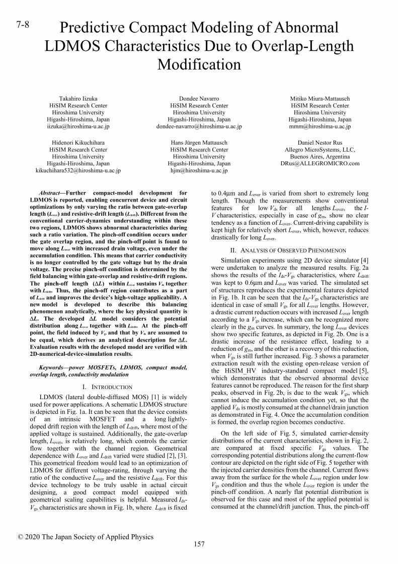
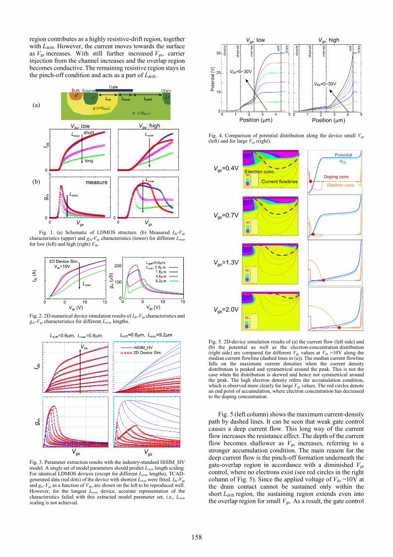
Simulation experiments using 2D device simulator [4] were undertaken to analyze the measured results. Fig. 2a shows the results of the Ids-Vgs characteristics, where Ldrift was kept to 0.6μm and Lover was varied. The simulated set of structures reproduces the experimental features depicted in Fig. 1b. It can be seen that the Ids-Vgs characteristics are identical in case of small Vgs for all Lover lengths. However, a drastic current reduction occurs with increased Lover length according to a Vgs increase, which can be recognized more clearly in the gm curves. In summary, the long Lover devices show two specific features, as depicted in Fig. 2b. One is a drastic increase of the resistance effect, leading to a reduction of gm, and the other is a recovery of this reduction, when Vgs is still further increased. Fig. 3 shows a parameter extraction result with the existing open-release version of the HiSIM_HV industry-standard compact model [5], which demonstrates that the observed abnormal device features cannot be reproduced. The reason for the first sharp peaks, observed in Fig. 2b, is due to the weak Vgs, which cannot induce the accumulation condition yet, so that the applied Vds is mostly consumed at the channel/drain junction as demonstrated in Fig. 4. Once the accumulation condition is formed, the overlap region becomes conductive.
On the left side of Fig. 5, simulated carrier-density distributions of the current characteristics, shown in Fig. 2, are compared at fixed specific Vgs values. The corresponding potential distributions along the current-flow contour are depicted on the right side of Fig. 5 together with the injected carrier densities from the channel. Current flows away from the surface for the whole Lover region under low Vgs condition and thus the whole Lover region is under the pinch-off condition. A nearly flat potential distribution is observed for this case and most of the applied potential is consumed at the channel/drift junction. Thus, the pinch-off
7-8
© 2020 The Japan Society of Applied Physics157
region contributes as a highly resistive-drift region, together with Ldrift. However, the current moves towards the surface as Vgs increases. With still further increased Vgs, carrier injection from the channel increases and the overlap region becomes conductive. The remaining resistive region stays in the pinch-off condition and acts as a part of Ldrift.
Fig. 1. (a) Schematic of LDMOS structure. (b) Measured Ids-Vgs characteristics (upper) and gm-Vgs characteristics (lower) for different Lover for low (left) and high (right) Vds.
Fig. 2. 2D numerical device simulation results of Ids-Vgs characteristics and gm-Vgs characteristics for different Lover lengths.
Fig. 3. Parameter extraction results with the industry-standard HiSIM_HV model. A single set of model parameters should predict Lover length scaling. For identical LDMOS devices (except for different Lover lengths), TCAD-generated data (red dots) of the device with shortest Lover were fitted. Ids-Vgs and gm-Vgs as a function of Vds, are shown on the left to be reproduced well. However, for the longest Lover device, accurate representation of the characteristics failed with this extracted model parameter set, i.e., Lover scaling is not achieved.
Fig. 4. Comparison of potential distribution along the device small Vgs (left) and for large Vgs (right).
Fig. 5. 2D-device simulation results of (a) the current flow (left side) and (b) the potential as well as the electron-concentration distribution(right side) are compared for different Vgs values at Vds =10V along themedian current flowline (dashed lines in (a)). The median current flowline falls on the maximum current densities when the current densitydistribution is peaked and symmetrical around the peak. This is not thecase when the distribution is skewed and hence not symmetrical aroundthe peak. The high electron density refers the accumulation condition,which is observed more clearly for large Vgs values. The red circles denote an end point of accumulation, where electron concentration has decreased to the doping concentration.
Fig. 5 (left column) shows the maximum current-density path by dashed lines. It can be seen that weak gate control causes a deep current flow. This long way of the current flow increases the resistance effect. The depth of the current flow becomes shallower as Vgs increases, referring to a stronger accumulation condition. The main reason for the deep current flow is the pinch-off formation underneath the gate-overlap region in accordance with a diminished Vgs control, where no electrons exist (see red circles in the right column of Fig. 5). Since the applied voltage of Vds =10V at the drain contact cannot be sustained only within the short Ldrift region, the sustaining region extends even into the overlap region for small Vgs. As a result, the gate control
(a)
(b)
158

of the current flow is limited to only within the non-pinch-off region, where injected carriers from the channel prolong the path to the electrode. The details of the observed pinch-off feature are determined by the balancing of the two fields, induced within the conductive gate-overlap region and within the pinch-off region.
III. MODELING OF ΔL AND VERIFICATION
Our task here is to develop a compact model for the pinch-off length ΔL in the lightly-doped resistive region under the gate. The pinch-off occurs at the point where the gate-oxide field becomes equal to the lateral electric field, and thus the lateral electric field starts to dominate beyond this point. Since HiSIM_HV solves the potential distribution along the device iteratively, the key potential value Vdp, referring the end of the gate control, is known as demonstrated in Fig. 6 [5]. Here the potential distribution is approximated by a quadratic function within the drift region as
( )2
0a x x bφ = + + (1)
2 2
2 2
2
dp
0
0
0
total
total
VaL L
Vb V
L xx
−
Δ = −
Δ ⋅ = −
(2)
ds dp
total over dri
0 over
V V VL L Lx L L
Δ = − = + = − Δ
(3)
An analytical equation for ΔL is derived as
2 2 2ov total
overov
V V E LL L
EΔ − Δ +
Δ = + (4)
( )oxov ov
si oxgE V c
Tφ= − −
(5)
where Eov is the field strength at the pinch-off point (x=0). The surface potential within Lover under the gate control φov is also calculated by solving the Poisson equation iteratively, which determines the electric field within Lover. An adjustable parameter c denotes the threshold voltage of the accumulation start. Therefore, the field strengths can be calculated analytically. Thus the current equation within the drift region is written as
ddpddp eff ov drift drift
drift
VI W X qN
L Lμ=
+ +ΔRDRDL1(6)
where Weff is the device width, Xov is the width of the current flow and μdrift is the carrier mobility within the drift region [5]. As can be seen, the pinch-off length ΔL is treated as an extension of the length of the resistive region [5], and thus ΔL reduces the electric field within the drift region. HiSIM considers the continuity condition between the channel current Ids and Iddp to determine Vdp [5], [6].
The pinch-off length ΔL is calculated and compared with 2D device simulations results in Fig. 7. It can be seen from Eq. (6), that a large ΔL for small Vgs leads to an increased resistance effect. Agreement of the model calculation results to those of 2D device simulation is quite well. Slight deviation of the Vgs dependence might be caused by the quadratic approximation of the potential distribution for deriving the analytical description of ΔL. To compensate this approximation, a model parameter could be introduced to obtain better fittings.
Fig. 6. Potential distribution along the device, as considered in HiSIM_HV. The internal-node potential Vdp refers the end of the gate control, namely, the pinch-off point for the presently studied case. Surface accumulation vanishes at the pinch-off point within the gate overlapped region.
Fig. 7. Comparison of ΔL as extracted with 2D-device simulation and calculated with developed model. The 2D-device simulation results of ΔL are extracted as the points, where the vertical component of electric field turns to negative from positive. The developed model assumes a quasi 1D potential distribution along the device, into which the electron distribution along the depth direction is practically integrated. In spite of the
159

assumptions introduced for deriving the analytical formulation, agreement is acceptable.
Figs. 8a and b compare the model-calculated I-V characteristics and gm with those of 2D-device simulation results. The model calculation is done only by introducing the ΔL values extracted in Fig. 7. The first sharp peak in gm for small Vgs refers to the condition that ΔL is nearly equal to Lover. According to the Vgs increase, ΔL approaches to zero, resulting in a lowering of the resistance effect and the start
of the gm recovery. After ΔL becomes zero, only the carrier mobility within the drift region determines the feature as demonstrated in Figs. 8c and 8d. In particular, Fig. 8c clearly shows that drain current depletes from that for ΔL=0. However, it reverts to that for ΔL=0 at higher Vgs.
Fig. 8. Comparison of I-V characteristics between the developed model (red line) and 2D-device simulation (blue symbols). a) Ids-Vgs and b) gm-Vgs, at Vds=10 V. The observed distinctive modulation in gm, has been captured by the developed compact model, while in Fig.3 it was completely misrepresented using the industry-starndard HiSIM_HV model, where the developed model for the ΔL modulation is not yet included. c) Ids-Vgs and d) gm-Vgs, at Vds=10 V, both with and withoutΔL.
REFERENCES
[1] J. D. Plummer and J. D. Meindl, IEEE JSSC vol. SC-11, no. 6, p.809, 1976.
[2] B. Wang et al.,IRPS 2005, p. 654.
[3] Y. Oritsuki et al., Nanotech 2009, Houston, May 3-7, 2009, p. 600.
[4] ATLAS User’s Manual, SILVACO, Inc., Santa Clara, CA, 2018.
[5] HiSIM_HV 2.4.0 User’s Manual, Hiroshima Univ., Hiroshima,Japan, 2017.
[6] H.J.Mattausch et al., IEEE TED vol.60, no.2, p.653, 2012.
(d)
(a)
(b)
(c)
160
Related Documents