Phil. Trans. R. Soc. A (2012) 370, 4089–4114 doi:10.1098/rsta.2011.0217 Precision surface measurement BY X. JIANG* Centre for Precision Technologies, School of Computing and Engineering, University of Huddersfield, Huddersfield, UK Surface size, geometry and texture are some of the most influential subjects in the fields of precision and ultra-precision engineering, defining the functional interface through which emerging products operate. Next-generation products demand super-smooth surfaces, freeform geometries or even deterministically introduced microstructures to provide functional performance. Technological progress using these surfaces types is possible only if the associated manufacturing processes are rigorously controlled and the surfaces are measurable. Metrology for advanced surfaces is not established. The current state of the art is challenged in respect to (i) surface characteristics, extremity of size, ultra precision, quality, geometric complexity, or combinations of these aspects, and (ii) measurement technology for the manufacturing environment, in particular, online, non-contact, high speed, ease of use, small footprint and robustness. This study addresses the challenges in this subject area and discusses some fundaments and principles derived from interdisciplinary research. The combination of these aspects is enabling the creation of manufacturing-environment-based measurement technology. This is expected to facilitate advanced surface manufacture over a wide range of sectors, including large science programmes and high-technology engineering. Keywords: precision measurement; optical interferometry; surfaces 1. Introduction Precision engineering is a multi-disciplinary scientific field that is always seeking ‘the next decimal place’. Surface measurement is one of the important subjects in precision engineering and it has steadily progressed alongside evolutionary precision technologies throughout past decades. Surface geometry and topography have significantly influenced many key areas such as pure and applied sciences, engineering and bioengineering. Examples include surfaces used in optics in high-power laser-energy systems, optics in earth/space-based large telescopes, interfaces in fluid dynamics (energy- efficient jet engines, aircraft fuselages and wings), long-life human-joint implants, microelectronics and microelectromechanical machines/nanoelectromechanical machines in nanotechnology applications. Surface geometry and topography are vital for the key components of science and engineering applications. Differing from conventional surfaces, the surfaces for high added value products may have complex freeforms (non-rotational and *[email protected] One contribution of 16 to a Discussion Meeting Issue ‘Ultra-precision engineering: from physics to manufacturing’. This journal is © 2012 The Royal Society 4089 on June 18, 2018 http://rsta.royalsocietypublishing.org/ Downloaded from

Welcome message from author
This document is posted to help you gain knowledge. Please leave a comment to let me know what you think about it! Share it to your friends and learn new things together.
Transcript
Phil. Trans. R. Soc. A (2012) 370, 4089–4114doi:10.1098/rsta.2011.0217
Precision surface measurementBY X. JIANG*
Centre for Precision Technologies, School of Computing and Engineering,University of Huddersfield, Huddersfield, UK
Surface size, geometry and texture are some of the most influential subjects in the fields ofprecision and ultra-precision engineering, defining the functional interface through whichemerging products operate. Next-generation products demand super-smooth surfaces,freeform geometries or even deterministically introduced microstructures to providefunctional performance. Technological progress using these surfaces types is possibleonly if the associated manufacturing processes are rigorously controlled and the surfacesare measurable. Metrology for advanced surfaces is not established. The current stateof the art is challenged in respect to (i) surface characteristics, extremity of size,ultra precision, quality, geometric complexity, or combinations of these aspects, and(ii) measurement technology for the manufacturing environment, in particular, online,non-contact, high speed, ease of use, small footprint and robustness. This study addressesthe challenges in this subject area and discusses some fundaments and principlesderived from interdisciplinary research. The combination of these aspects is enabling thecreation of manufacturing-environment-based measurement technology. This is expectedto facilitate advanced surface manufacture over a wide range of sectors, including largescience programmes and high-technology engineering.
Keywords: precision measurement; optical interferometry; surfaces
1. Introduction
Precision engineering is a multi-disciplinary scientific field that is alwaysseeking ‘the next decimal place’. Surface measurement is one of theimportant subjects in precision engineering and it has steadily progressedalongside evolutionary precision technologies throughout past decades. Surfacegeometry and topography have significantly influenced many key areas suchas pure and applied sciences, engineering and bioengineering. Examplesinclude surfaces used in optics in high-power laser-energy systems, opticsin earth/space-based large telescopes, interfaces in fluid dynamics (energy-efficient jet engines, aircraft fuselages and wings), long-life human-joint implants,microelectronics and microelectromechanical machines/nanoelectromechanicalmachines in nanotechnology applications.
Surface geometry and topography are vital for the key components of scienceand engineering applications. Differing from conventional surfaces, the surfacesfor high added value products may have complex freeforms (non-rotational and*[email protected]
One contribution of 16 to a Discussion Meeting Issue ‘Ultra-precision engineering: from physics tomanufacturing’.
This journal is © 2012 The Royal Society4089
on June 18, 2018http://rsta.royalsocietypublishing.org/Downloaded from
4090 X. Jiang
non-translational symmetric) up to 1–2 m in size with one part in 108 surfacetopography; some have very accurate surfaces but small size, and work in extremeenvironmental conditions; some have deterministic structures; others result fromthe merging of dimensional geometry with surface texture [1].
These examples confront the state-of-the-art in surface measurement sciencein terms of: (i) surface characteristics, extremity of size, ultra precision, quality,geometry complexity, or combinations of these aspects, and (ii) measurementtechnology for the manufacturing environment, in particular, online, non-contact, high speed, ease of use, small footprint and robustness. Developing themeasurement capability necessary to perform quantitative measurements on thesurfaces types listed earlier, with the required assessment conditions and speed,is very challenging.
(a) Manufacturing challenges
The continuing evolution of high-precision manufacture is placing evermoreneed to perform surface measurement in the manufacturing environment.Example areas include the following.
— Advanced and emerging products from many sectors have large-scale(up to metres) ultra-precision (nanometre tolerance) components withcomplex surfaces. For example, micro moulding (e.g. aspheric lenses)produces a large amount of small components. These manufacturedproducts need individual sample measurement without removal fromthe machine tool/production line. Batch sampling is not sufficient toprovide consistency and quality, so high-speed, automated measurementis critical.
— Online measurement either for the form of a freeform surface for keyscience objects, such as telescope mirror segments (surface roughnessless than 5 nm r.m.s., form accuracy less than 25 nm r.m.s. over 1–2 msize) [2] and nanostructures on large-scale substrates (e.g. photovoltaicpanels, reel to reel thin film) [3], with the speed necessary for affordablemanufacture does not exist. For such a high level of surface accuracy,offline measurement using state-of-the-art laboratory instruments is notapplicable. If an expensive trial-and-error approach is used, measurementcan take up a substantial fraction of the cycle time for precision surfacefabrication, as high as 90 per cent in the final stages of finishing a largeoptical surface segment for instance [4]; it is more difficult for largesubstrate manufacture, which requires quality control simultaneously withcontinuous production processes [5].
— The assessment of geometry and surface topography of small objects,for example, inertial-confinement fusion shells in high-power laser fusionsystems, especially in terms of the required measurement speed, iscurrently lacking. It has been verified that surface imperfections of theseshells grow and can lead to an asymmetric implosion or even shell break-up and, as such, the measurement the topography of every target shellis extremely important for a successful fusion reaction. Currently, atomicforce microscopy (AFM)-based offline measurement takes 2.5 h to measurea 2 mm diameter shell. This evaluation method constitutes a qualitative
Phil. Trans. R. Soc. A (2012)
on June 18, 2018http://rsta.royalsocietypublishing.org/Downloaded from

Precision surface measurement 4091
description and does not provide any information for the control of themanufacturing process [6].
— Currently, quantitative surface metrology techniques provide the basis forinspection of the majority of micro and nanoscale surface topographypresent on large area substrates. They have demonstrated capabilityto measure surfaces at the sub-micro/nanoscale. However, almostwithout exception, these measurement techniques are confined tolaboratory environments. Integration of measurement systems withinthe manufacturing process provides a particular challenge with regardto online, non-contact, high speed, ease of use, small footprint androbustness [7].
— There are clear technology gaps to be bridged for the evolution oflaboratory-based measurement systems into the application within themanufacturing environment to provide inline/on-process measurement: (i)capability of achieving the required measurement resolution in the verticaland lateral scales, (ii) tolerance in terms of performance owing to themanufacturing environment, (iii) a fast measurement response withoutundue pressure on production time, and (iv) demonstrable measurementtraceability and uncertainty [8].
(b) State of the art
Measurement of geometrical surfaces is mature for ‘planar’ (Euclidean)surfaces, i.e. to say for surfaces that can be defined by a single height valuefor each point in a plane [1]. Mature laboratory-based instruments adopt a widerange of principles [9]. Stylus profilometry provides the current state of the artin terms of vertical range (12.5 mm) versus resolution (2 nm), but is very slow[10]. The lateral resolution is dependent on reducing the stylus radius, whichalso increases the likelihood of scratching, making the metrology destructivein many cases. Low-force-stylus-based methods aim to expand the potential ofcontact measurement to delicate, micro-featured surfaces as well as increasingmeasurement speed [11,12]. Scanning probe microscopy techniques, particularlyAFM, provide the ultimate in terms of lateral resolution. These techniques arenotoriously difficult to apply and are severely limited in terms of speed/range/tipwear [13].
Optical techniques cover a large number of differing techniques, many ofwhich are very well established in high-precision manufacturing because oftheir sensitivity, non-destructive nature and relative speed [14]. Optical methodsare most likely to provide the best avenue to meet metrology requirementsfor precision surface manufacture. In many cases, it is not possible to usecontact-based metrology without damaging the surface. For those types ofmanufacturing processes that require metrology in batches, the inherent speedof the majority of optical methods is essential. Certainly, the most prevalentoptical technology for surface metrology is the scanning white-light interferometer(SWLI). Commercially available instrumentation based on SWLI can provideareal topographic information with nanometre uncertainty over 200 mm verticalrange. Larger vertical ranges may be traded for higher measurement uncertainty.Measurement times are several tens of seconds depending on the vertical rangeto be covered.
Phil. Trans. R. Soc. A (2012)
on June 18, 2018http://rsta.royalsocietypublishing.org/Downloaded from
4092 X. Jiang
While SWLI is currently the de facto technique for optical interrogation ofmany advanced surfaces, it is often found to be somewhat slow, especially overlarge vertical ranges. Some recent commercial advances have increased the speedof data acquisition and objective scanning [15], and also some work is beingcarried out in order to increase the data efficiency of SWLI [16]. Nevertheless,SWLI techniques are always limited by the need to physically move the objectivelens (or sample) through the vertical measurement range.
SWLI is, of course, not only the established technique for surface metrology,but it is also one of the most flexible. Many other techniques however play animportant role in specific areas. A phase-shifting interferometer (PSI) providesthe ultimate in terms of vertical resolution, but is limited to smooth surfaceshaving no discontinuities larger than half the source light wavelength [17]. Thismay be extended by the use of synthetic wavelengths, but generally the extendedvertical range is at the cost of vertical resolution [18]. Frequency stability of thelight sources becomes increasingly problematic as more wavelengths are added[19]. Fringe projection techniques are being applied to determine local slope ofsurfaces down to the nanoscale, but these are limited to fringe ambiguity problemsin the same way as PSI, while at the same time being less traceable [20].
Some single-point measurement methods have good potential for onlineapplications by virtue of small probe footprints and the ability to mountthem remotely using fibre links in some cases. Instruments based on confocaltechniques such as focus follow [21] and chromatic aberration probing [22]are attractive for their long depth of focus. They do not reach the samelevels of resolution or traceability as interferometry however, and the formerrequires mechanical movement within the probe head. Synthetic wavelengthtechniques can provide single-point probes with enhanced traceability and nomechanical movement, but the same limitations are present as for their bulkoptic counterparts [23].
The instruments above cover surface measurement from nano to microscale, butalmost all operate in a laboratory environment. They are powerful in their abilityto derive surface geometry at various scales, but the measurement speed, physicalfootprint and system complexity are the primary factors in limiting potential formanufacturing environment applications.
In this paper, systemic building blocks, based on some fundamentaltechniques from multi-disciplinary fields, are discussed. New optical principles,wavelength/frequency-scanning techniques, derived from the fundaments arepresented. The aim for this investigation was to create next-generation ultra-precision/nanoscale surface instrumentation to retrieve information on thetopography and geometry of precision surfaces in a very fast, accurate and robustway with a potential for providing online capable measurement and facilitatingmanufacturing environment applications.
2. Fundaments and principles
This section outlines these basic fundaments and principles that have beeninvestigated to seek new methods which could be used to build the next-generation surface measurement systems.
Phil. Trans. R. Soc. A (2012)
on June 18, 2018http://rsta.royalsocietypublishing.org/Downloaded from

Precision surface measurement 4093
(a) Multi-wavelength scanning interferometry (tech I )
This method uses a tunable laser to create a series of interferograms froman interferometer. A tunable laser is able to provide a range of wavelengths, l,of quasi-monochromatic light. In reality, the mode spacing of the laser cavitymeans that these tuned wavelengths are approximately discrete, the laser ‘hops’to specific wavelength values over the tuning range I (lj): j = 1, 2 . . . J . As such,a Michelson interferometer sourced by a tunable laser will have an outputintensity function
I (lj) = Ir(lj) + Im(lj) + 2√
Ir(lj)Im(lj)|g(t)| cos q(lj), (2.1)
neglecting for the moment any spatial relationship for clarity. Ir and Im arethe reference and measurement arm intensities, respectively. g(t) is the complexdegree of coherence and depends on the overall time delay, t, between the twoarms. This is a complex quantity having a phase, 4, that represents the phasedifference between the interfering light.
In a high-quality, tunable laser source having a line width of a few megahertz,the coherence length is several metres at least. This is much longer than the phasedifferences to be investigated in optical surface metrology, and as such, it maybe assumed that |g(t)| = 1 for all t over the range of interest. If IDC = Ir(lj) +Im(lj) is a DC term formed by the addition of the intensities returning from eachinterferometer arm and IAC = 2
√Ir(lj)Im(lj) is an AC component describing the
amplitude of the modulated fringe intensity, equation (2.1) can be rewritten in asimplified form,
I (lj) = IDC(lj) + IAC(lj) cos q(lj). (2.2)
The intensity varies with wavelength owing to the output spectrum of the laserand any wavelength-dependent absorption or reflection from components in eacharm. If the laser remains quasi-monochromatic throughout the tuning range, itis reasonable to assume that the magnitude of the complex degree of coherenceis constant and unity. The phase however is dependent on the wavelength as
q(lj) = 4p(h + x)lj
, (2.3)
where x is a phase offset relating to the reflection and transmission properties inthe interferometer arms, as well as their lengths relative to each other. h is theoptical path difference due to sample surface height (in a surface measurementapplication). The phase offset quantity x may be viewed as constant offset,assuming it is constant across the field of view. Generally, it is preferable tokeep x as close to zero as possible for most wavelength scanning applications,thus avoiding a constant phase ramp in the result. Equation (2.3) is sometimessimplified further by introducing a fringe frequency term, Kj = 4p/lj .
(b) Self-calibration interferometry (tech II )
Self-calibration techniques using common path (or near common path)interferometry and active stabilization techniques can reduce sensitivity todisturbance. This can allow the subsequent reduction of complexity and mass
Phil. Trans. R. Soc. A (2012)
on June 18, 2018http://rsta.royalsocietypublishing.org/Downloaded from
4094 X. Jiang
of an instrument, as well as increasing the range of environments in which it maybe expected to perform acceptably.
The output of any interferometer is subject to a time-varying phase term 3(t),which is due to environmental disturbance altering either the physical path lengthor the refractive index of the transmission medium (usually air),
I (l, t) = IDC(l, t) + IAC(l, t) cos[q(l) + 3(t)]. (2.4)
This time-varying error term may be tracked by a reference interferometerassuming that any interrogation technique has sufficient bandwidth. Ifthis reference interferometer has a common path with the measurementinterferometer, then the tracked phase is the error term, 3(t), that is present inboth interferometers. This error term may then either be removed at the signal-processing stage, or used as the feedback parameter in a control loop. In the lattercase, the phase must be physically altered and this may be performed by, forinstance, a piezo-mounted mirror or an electro-optic phase modulator (EOPM)placed in one arm.
(c) Wavelength dispersive multiplexing (tech III )
A dispersive optical element can be used to cause the spatial separationof wavelengths emitted from an interferometer. In this case, it is possible tointerrogate a specific point on a surface with a specific wavelength. Assuminga one-to-one mapping of wavelength to a surface position, which may be ensuredby the careful choice of a dispersive element, the equation for the interferometeroutput may be rewritten as
Ixi (lj) = IDCxj (lj) + IACxj (lj) cos[Kjh(xj)], where x = f (l) (2.5)
and f is some function describing the position-to-wavelength response of thedispersive probe in use and its specific parameters. The surface height, h, is nowthat height interrogated at some position along a profile, x , as dictated by thecurrent tuned wavelength. Here, the phase offset, x, is assumed to be zero acrossthe field of view.
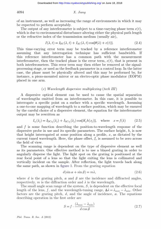
The scanning range is dependent on the type of dispersive element as wellas its parameters. One effective method is to use a blazed grating in order toangularly disperse the light. The light spot on the grating is positioned at therear focal point of a lens so that the light exiting the lens is collimated andvertically incident on the sample. After reflection, the light travels back alongthe same path, as shown in figure 1. From the grating equation
d(sin a + sin b) = ml, (2.6)
where d is the grating pitch, a and b are the incidence and diffracted angles,respectively, m is the diffraction order and l is the wavelength.
The small angle scan range of the system, S , is dependent on the effective focallength of the lens, f , and the wavelength-tuning range, Dl = lmax − lmin. Otherfactors are the grating pitch, d, and the angle of incidence, a. The equationsdescribing operation in the first order are
S = f · (lmax − lmin)d cos b
(2.7)
Phil. Trans. R. Soc. A (2012)
on June 18, 2018http://rsta.royalsocietypublishing.org/Downloaded from
Precision surface measurement 4095
3 dB couplerMFI
OSA
GRINabi
fmirror
blazed grating
objective lens
Figure 1. Wavelength scanning using blazed diffraction grating. GRIN, graded index; MFI,multiplexed fibre interferometer; OSA, optical spectrum analyser.
and
b = sin−1(
ml
d− sin a
). (2.8)
If b is kept small, the physical translation of the spot on the measurand surfacewill change, to a good approximation, linearly with wavelength. Although theeffective focal length, grating pitch and wavelength range are fixed quantities inany system, it is possible to adjust the angle of incidence, a, in order to changethe scan range.
(d) Wavelength absolute measurement (tech IV )
Source wavelength scanning can be applied to a Michelson interferometer forpurposes of determining the absolute optical path length difference between thetwo arms. First, it is often convenient to rewrite the interferometer equation (2.2)in terms of a discrete angular wavenumber, km = 2p/lj , with m = 1, 2 . . . M . Thisleads to
I (km) = I ′DC(km) + I ′
AC(km) cos q(km). (2.9)
Looking at equation (2.9), it can be seen that wavenumber scanning will resultin phase cycling if the interferometer is not perfectly matched. The frequency ofthe phase cycling is determined by the sample height, h, and the phase offset, x.If the phase offset is zero and constant across the field of view, the sample heightmay then be determined by
h = Dq
2(kM − k0), (2.10)
for M discrete wavenumber steps. One requirement is that the phase mustnot change by more than p radians between each wavenumber step or aliasingwill occur.
If the wavenumber is scanned and an interferogram recorded at each of thediscrete scanned wavenumber values, the optical path difference and thus surfaceheight may be determined.
Phil. Trans. R. Soc. A (2012)
on June 18, 2018http://rsta.royalsocietypublishing.org/Downloaded from
4096 X. Jiang
(e) ‘Lab-on-a-chip’ microsystems (tech V )
‘Lab-on-a-chip’ microsystems permit the integration of several sequentialexperimental steps into a single automated process to perform more analysisover a unit time at a lower cost per analysis. They offer several advantages overconventional analytical techniques such as large autonomy owing to eliminationand simplification of external instruments, minimal sample requirements, rapidanalysis time, ease-of-use, minimized exposure to hazardous materials, reducedwaste generation and also much lower cost. Progress in integrated opticstechnology, including critically, increased automation in device construction, willallow the design and building of more complex and efficient ‘Lab-on-a-chip’microsystems at a reduced cost.
The ‘Lab-on-a-chip’ concept is being applied to the multi-disciplinary fields ofchemistry, biology, optics and microelectronics. It concerns the miniaturizationand the integration of complex systems on a small substrate of silicon, glassor plastic. The latest technology allows the passive assembly of single-modeoptical components made from different material systems by way of location andalignment artefacts created by technologies such as deep etching.
3. Online/inline precision surface measurement systems
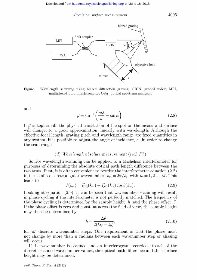
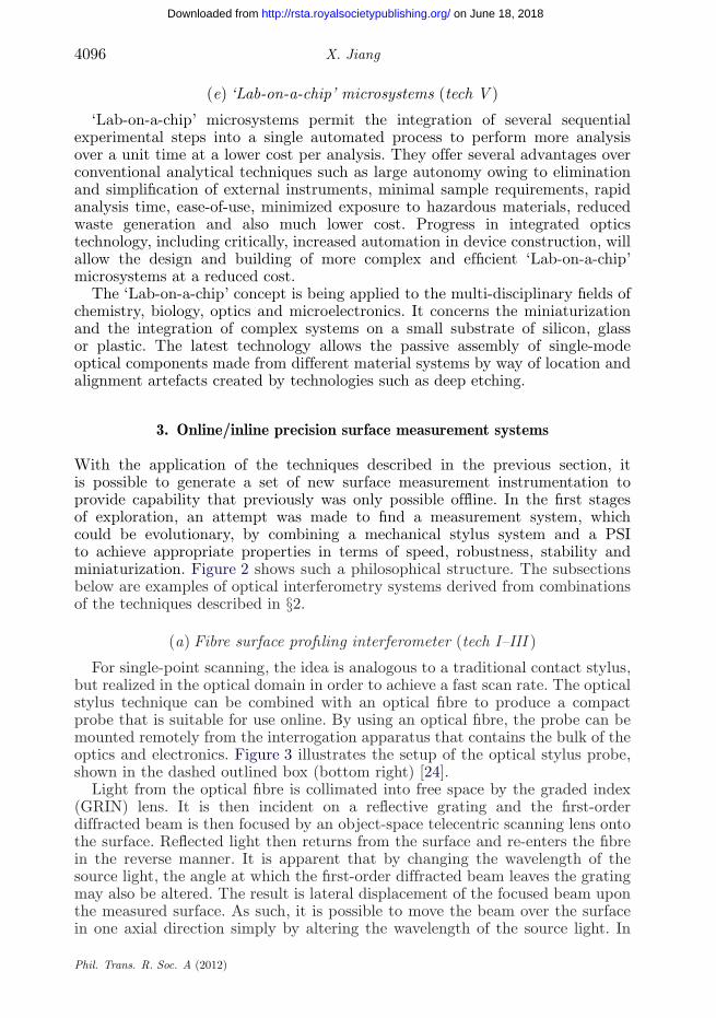
With the application of the techniques described in the previous section, itis possible to generate a set of new surface measurement instrumentation toprovide capability that previously was only possible offline. In the first stagesof exploration, an attempt was made to find a measurement system, whichcould be evolutionary, by combining a mechanical stylus system and a PSIto achieve appropriate properties in terms of speed, robustness, stability andminiaturization. Figure 2 shows such a philosophical structure. The subsectionsbelow are examples of optical interferometry systems derived from combinationsof the techniques described in §2.
(a) Fibre surface profiling interferometer (tech I–III )
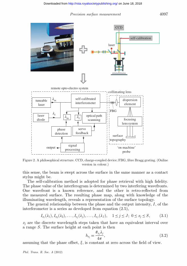
For single-point scanning, the idea is analogous to a traditional contact stylus,but realized in the optical domain in order to achieve a fast scan rate. The opticalstylus technique can be combined with an optical fibre to produce a compactprobe that is suitable for use online. By using an optical fibre, the probe can bemounted remotely from the interrogation apparatus that contains the bulk of theoptics and electronics. Figure 3 illustrates the setup of the optical stylus probe,shown in the dashed outlined box (bottom right) [24].
Light from the optical fibre is collimated into free space by the graded index(GRIN) lens. It is then incident on a reflective grating and the first-orderdiffracted beam is then focused by an object-space telecentric scanning lens ontothe surface. Reflected light then returns from the surface and re-enters the fibrein the reverse manner. It is apparent that by changing the wavelength of thesource light, the angle at which the first-order diffracted beam leaves the gratingmay also be altered. The result is lateral displacement of the focused beam uponthe measured surface. As such, it is possible to move the beam over the surfacein one axial direction simply by altering the wavelength of the source light. In
Phil. Trans. R. Soc. A (2012)
on June 18, 2018http://rsta.royalsocietypublishing.org/Downloaded from
Precision surface measurement 4097
laser
CCD
self-calibration
laserdiode
remote opto-electro systemcollimating lens
‘on machine’probe
output
dispersionelement
surfacetopography
tuneablelaser
self-calibratedinterferometer
optical pathscanning
phasedetection
servofeedback
signalprocessing
FBG
focusinglens system
lm
lm
lflf
Figure 2. A philosophical structure. CCD, charge-coupled device; FBG, fibre Bragg grating. (Onlineversion in colour.)
this sense, the beam is swept across the surface in the same manner as a contactstylus might be.
The self-calibration method is adopted for phase retrieval with high fidelity.The phase value of the interferogram is determined by two interfering wavefronts.One wavefront is a known reference, and the other is retro-reflected fromthe measured surface. The resulting phase map, along with knowledge of theilluminating wavelength, reveals a representation of the surface topology.
The general relationship between the phase and the output intensity, I , of theinterferometer is a series as developed from equation (2.5),
Ix1(l1), Ix2(l2), . . . , Ixj (lj), . . . , IxJ (lJ ), 1 ≤ j ≤ J ; 0 ≤ xj ≤ S , (3.1)
xj are the discrete wavelength steps taken that have an equivalent interval overa range S . The surface height at each point is then
hxj = qxj lj
4p, (3.2)
assuming that the phase offset, x, is constant at zero across the field of view.
Phil. Trans. R. Soc. A (2012)
on June 18, 2018http://rsta.royalsocietypublishing.org/Downloaded from

4098 X. Jiang
TMS320F2812 DSP
EOM driver board12 bitA/D
12 bitA/D
eight sampleaverage
eight sampleaverage
four wordbuffer
four wordbuffer
PCGPIB
interface
tuneable lasersource
laser diode 3 dB coupler
3 dB coupler
FBG
PINdetector
transimpedanceamplifier board
buffer
buffer
×50 k
×50 k
PINdetector surface
collimatinglens
parallelinterface
SPIinterface
16 bitD/A
REF mirror
GRIN lens
EOM
optical probediffractiongrating
GRIN lens
×3
±12V
+
circulator
circulator
1
3
1 2
3
2
500 wordbuffer
PSIalgorithm
PIDalgorithm
stepwaveformgenerator
lmlm + lr
lm + lr
lm + lr
lr
lr lm
lr
lm
Figure 3. Surface profiling interferometer. A/D, analogue to digital convertor; D/A, digital toanalogue convertor; EOM, electro-optic (phase) modulator; GPIB, general purpose interface bus;PIN, p–i–n photodetector. (Online version in colour.)
The ability to use fibre interferometry provides the major advantage ofbeing able to mount a compact probe head remotely from the rest of theinstrumentation. However, implementing optical fibre interferometers creates initself a particular set of challenges. It is well documented that fibre interferometerssuffer from major instabilities brought about by environmental effects [25].Temperature variations and vibration cause deformation and stresses in thefibre core, resulting in changes in the optical path length. Path length changeson a macrolevel result in an additive error to the phase to be measured; those ona microlevel contribute thermodynamic phase noise to the output [26]. Randompolarization state evolution is also another problem that can cause difficulty foracquiring stable measurement [27]. Mitigating the effects of all these disturbancesis essential, if any meaningful surface height information is to be obtained fromthe acquired phase data.
Phil. Trans. R. Soc. A (2012)
on June 18, 2018http://rsta.royalsocietypublishing.org/Downloaded from
Precision surface measurement 4099
wavelength (nm)
prof
ile p
ositi
on, x
10
8
6
4
2
01560 1565 1570 1575 1580
25
a
25.5262730
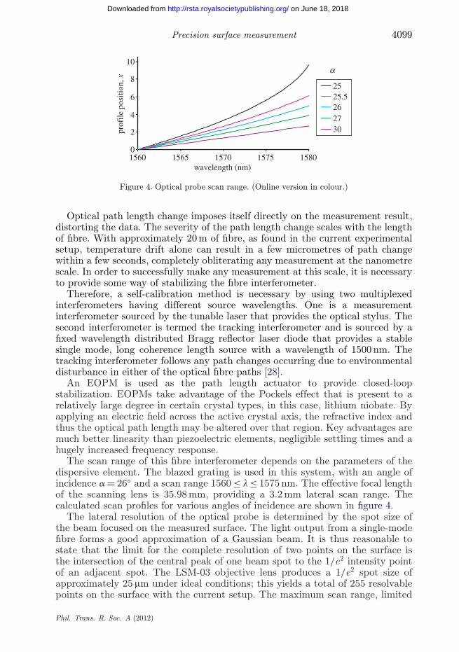
Figure 4. Optical probe scan range. (Online version in colour.)
Optical path length change imposes itself directly on the measurement result,distorting the data. The severity of the path length change scales with the lengthof fibre. With approximately 20 m of fibre, as found in the current experimentalsetup, temperature drift alone can result in a few micrometres of path changewithin a few seconds, completely obliterating any measurement at the nanometrescale. In order to successfully make any measurement at this scale, it is necessaryto provide some way of stabilizing the fibre interferometer.
Therefore, a self-calibration method is necessary by using two multiplexedinterferometers having different source wavelengths. One is a measurementinterferometer sourced by the tunable laser that provides the optical stylus. Thesecond interferometer is termed the tracking interferometer and is sourced by afixed wavelength distributed Bragg reflector laser diode that provides a stablesingle mode, long coherence length source with a wavelength of 1500 nm. Thetracking interferometer follows any path changes occurring due to environmentaldisturbance in either of the optical fibre paths [28].
An EOPM is used as the path length actuator to provide closed-loopstabilization. EOPMs take advantage of the Pockels effect that is present to arelatively large degree in certain crystal types, in this case, lithium niobate. Byapplying an electric field across the active crystal axis, the refractive index andthus the optical path length may be altered over that region. Key advantages aremuch better linearity than piezoelectric elements, negligible settling times and ahugely increased frequency response.
The scan range of this fibre interferometer depends on the parameters of thedispersive element. The blazed grating is used in this system, with an angle ofincidence a = 26◦ and a scan range 1560 ≤ l ≤ 1575 nm. The effective focal lengthof the scanning lens is 35.98 mm, providing a 3.2 mm lateral scan range. Thecalculated scan profiles for various angles of incidence are shown in figure 4.
The lateral resolution of the optical probe is determined by the spot size ofthe beam focused on the measured surface. The light output from a single-modefibre forms a good approximation of a Gaussian beam. It is thus reasonable tostate that the limit for the complete resolution of two points on the surface isthe intersection of the central peak of one beam spot to the 1/e2 intensity pointof an adjacent spot. The LSM-03 objective lens produces a 1/e2 spot size ofapproximately 25 mm under ideal conditions; this yields a total of 255 resolvablepoints on the surface with the current setup. The maximum scan range, limited
Phil. Trans. R. Soc. A (2012)
on June 18, 2018http://rsta.royalsocietypublishing.org/Downloaded from
4100 X. Jiang
Ref. laser532 nm
coupler 1
coupler 2
circulator 1
circulator 2
GRIN 1
GRIN 2
PZT
ref. mirror
detector 1
detector 2
phasedetection
1 2
3
1FBG
23
lens 1
sampleAOD1
AOD2
lens 2
He–Ne laser633 nm
servoelectronics
l¢m
l¢m
lm
lr
lr
lr
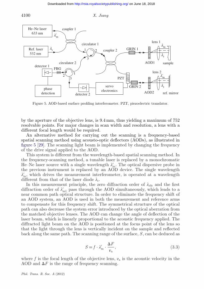
Figure 5. AOD-based surface profiling interferometer. PZT, piezoelectric translator.
by the aperture of the objective lens, is 9.4 mm, thus yielding a maximum of 752resolvable points. For major changes in scan width and resolution, a lens with adifferent focal length would be required.
An alternative method for carrying out the scanning is a frequency-basedspatial scanning method using acousto-optic deflectors (AODs), as illustrated infigure 5 [29]. The scanning light beam is implemented by changing the frequencyof the drive signal applied to the AOD.
This system is different from the wavelength-based spatial scanning method. Inthe frequency-scanning method, a tunable laser is replaced by a monochromaticHe–Ne laser source with a single wavelength l′
m. The optical dispersive probe inthe previous instrument is replaced by an AOD device. The single wavelengthl′
m, which drives the measurement interferometer, is operated at a wavelengthdifferent from that of the laser diode lr.
In this measurement principle, the zero diffraction order of lr0r and the firstdiffraction order of l′
m1 pass through the AOD simultaneously, which leads to anear common path optical structure. In order to eliminate the frequency shift ofan AOD system, an AOD is used in both the measurement and reference armsto compensate for this frequency shift. The symmetrical structure of the opticalpath can also decrease the system error introduced by the optical aberration fromthe matched objective lenses. The AOD can change the angle of deflection of thelaser beam, which is linearly proportional to the acoustic frequency applied. Thediffracted light beam on the AOD is positioned at the focus point of the lens sothat the light through the lens is vertically incident on the sample and reflectedback along the same path. The scanning range of the surface, S , can be deduced as
S = f · l′m · DF
va, (3.3)
where f is the focal length of the objective lens, ya is the acoustic velocity in theAOD and DF is the range of frequency scanning.
Phil. Trans. R. Soc. A (2012)
on June 18, 2018http://rsta.royalsocietypublishing.org/Downloaded from
Precision surface measurement 4101
laser diodedirectional
coupler
tuneable laser
Bthin film filter
photo detector 1 photo detector 2
directionalcoupler
directionalcoupler
isolator directionalcoupler A
phase grating sample
objective lens
object
I1 I1
I1/I2
I2
l1...ln l0
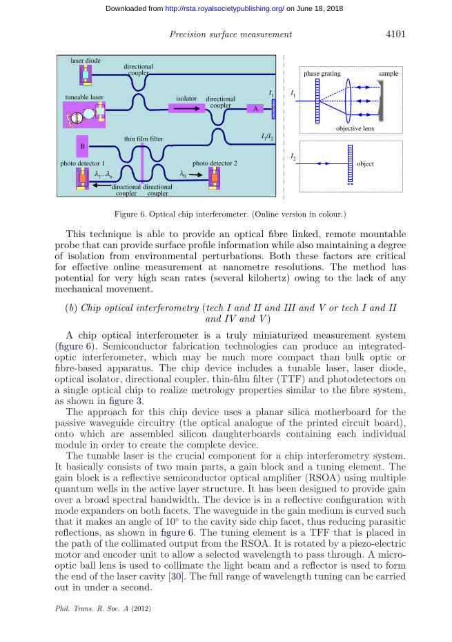
Figure 6. Optical chip interferometer. (Online version in colour.)
This technique is able to provide an optical fibre linked, remote mountableprobe that can provide surface profile information while also maintaining a degreeof isolation from environmental perturbations. Both these factors are criticalfor effective online measurement at nanometre resolutions. The method haspotential for very high scan rates (several kilohertz) owing to the lack of anymechanical movement.
(b) Chip optical interferometry (tech I and II and III and V or tech I and IIand IV and V )
A chip optical interferometer is a truly miniaturized measurement system(figure 6). Semiconductor fabrication technologies can produce an integrated-optic interferometer, which may be much more compact than bulk optic orfibre-based apparatus. The chip device includes a tunable laser, laser diode,optical isolator, directional coupler, thin-film filter (TTF) and photodetectors ona single optical chip to realize metrology properties similar to the fibre system,as shown in figure 3.
The approach for this chip device uses a planar silica motherboard for thepassive waveguide circuitry (the optical analogue of the printed circuit board),onto which are assembled silicon daughterboards containing each individualmodule in order to create the complete device.
The tunable laser is the crucial component for a chip interferometry system.It basically consists of two main parts, a gain block and a tuning element. Thegain block is a reflective semiconductor optical amplifier (RSOA) using multiplequantum wells in the active layer structure. It has been designed to provide gainover a broad spectral bandwidth. The device is in a reflective configuration withmode expanders on both facets. The waveguide in the gain medium is curved suchthat it makes an angle of 10◦ to the cavity side chip facet, thus reducing parasiticreflections, as shown in figure 6. The tuning element is a TFF that is placed inthe path of the collimated output from the RSOA. It is rotated by a piezo-electricmotor and encoder unit to allow a selected wavelength to pass through. A micro-optic ball lens is used to collimate the light beam and a reflector is used to formthe end of the laser cavity [30]. The full range of wavelength tuning can be carriedout in under a second.
Phil. Trans. R. Soc. A (2012)
on June 18, 2018http://rsta.royalsocietypublishing.org/Downloaded from

4102 X. Jiang
wavelength (nm)
outp
ut p
ower
(dB
m)
1500–60
1520 1540 1560 1580 1600
–50
–40
–30
–20
–10
0
10
Figure 7. The output power and the working wavelength of the tunable laser. (Online versionin colour.)
Two possible modes of operation are possible with the chip interferometrysystem. Firstly, a wavelength multiplexed scanning head, using a grating andcollimating objective lens can be used to acquire a surface profile, as described in§2c: tech III. Secondly, a Fizeau-type head may be used, which, when combinedwith the wavelength scanning supplied by the tunable laser, can provide absolutedistance measurements of a single point in a manner similar to that shown in§2d: tech IV.
A large wavelength-tuning range, a reasonably high output power and stablesingle longitudinal mode operation are all important for surface measurementsusing interferometry. The test results of the output power as a function of thewavelength of the chip tunable laser at a drive current of 250 mA are shownin figure 7. It can be seen that the output power is close to 0 dBm (1 mW) atwavelengths over the whole tuning range of 92 nm (1500–1590 nm), as shown infigure 7. The maximum output available from the laser is approximately 5 mW.
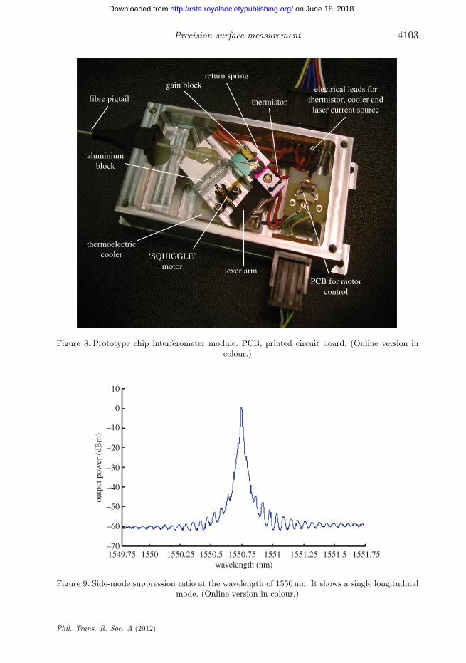
Figure 8 shows the tunable laser packaged into a daughterboard. Figure 9shows a single tuned longitudinal mode from the laser, the side-mode suppressionratio at 1550 nm is more than 45 dB.
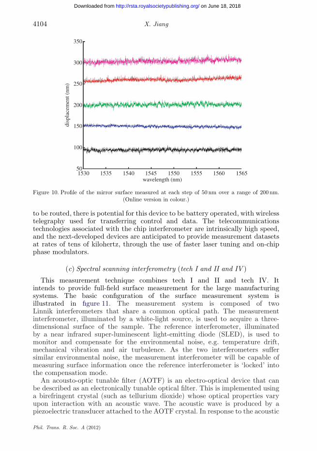
In order to ascertain the accuracy of the system setup, a piezoelectric translator(PZT) was used to displace the reference mirror in 50 nm steps over a 200 nmrange. The profile of the mirror surface at the same position was measured aftereach step. The difference between each consecutive step was then taken and isplotted in figure 10. It can be seen that the displacement between each consecutivestep is approximately 50 nm. The displacement data at each consecutive stepwere then averaged and a linear fit made to the data. The standard deviation ofthe average displacement data from the linear fit is 3.21 nm.
This measurement technology has the advantage for online measurementwhere miniature size is essential for embedding the metrology tool onto themanufacturing platform. Specifically where access makes it impossible for cables
Phil. Trans. R. Soc. A (2012)
on June 18, 2018http://rsta.royalsocietypublishing.org/Downloaded from
Precision surface measurement 4103
gain block
‘SQUIGGLE’motor
electrical leads forthermistor, cooler andlaser current source
PCB for motorcontrol
thermoelectriccooler
thermistorfibre pigtail
aluminiumblock
lever arm
return spring
Figure 8. Prototype chip interferometer module. PCB, printed circuit board. (Online version incolour.)
10
0
–10
–20
–30
–40
–50
–60
–701549.75 1550 1550.25 1550.5
wavelength (nm)
outp
ut p
ower
(dB
m)
1550.75 1551 1551.25 1551.5 1551.75
Figure 9. Side-mode suppression ratio at the wavelength of 1550 nm. It shows a single longitudinalmode. (Online version in colour.)
Phil. Trans. R. Soc. A (2012)
on June 18, 2018http://rsta.royalsocietypublishing.org/Downloaded from
4104 X. Jiang
350
300
250
200
150
100
501530 1535 1540 1545 1550
wavelength (nm)
disp
lace
men
t (nm
)
1555 1560 1565
Figure 10. Profile of the mirror surface measured at each step of 50 nm over a range of 200 nm.(Online version in colour.)
to be routed, there is potential for this device to be battery operated, with wirelesstelegraphy used for transferring control and data. The telecommunicationstechnologies associated with the chip interferometer are intrinsically high speed,and the next-developed devices are anticipated to provide measurement datasetsat rates of tens of kilohertz, through the use of faster laser tuning and on-chipphase modulators.
(c) Spectral scanning interferometry (tech I and II and IV )
This measurement technique combines tech I and II and tech IV. Itintends to provide full-field surface measurement for the large manufacturingsystems. The basic configuration of the surface measurement system isillustrated in figure 11. The measurement system is composed of twoLinnik interferometers that share a common optical path. The measurementinterferometer, illuminated by a white-light source, is used to acquire a three-dimensional surface of the sample. The reference interferometer, illuminatedby a near infrared super-luminescent light-emitting diode (SLED), is used tomonitor and compensate for the environmental noise, e.g. temperature drift,mechanical vibration and air turbulence. As the two interferometers suffersimilar environmental noise, the measurement interferometer will be capable ofmeasuring surface information once the reference interferometer is ‘locked’ intothe compensation mode.
An acousto-optic tunable filter (AOTF) is an electro-optical device that canbe described as an electronically tunable optical filter. This is implemented usinga birefringent crystal (such as tellurium dioxide) whose optical properties varyupon interaction with an acoustic wave. The acoustic wave is produced by apiezoelectric transducer attached to the AOTF crystal. In response to the acoustic
Phil. Trans. R. Soc. A (2012)
on June 18, 2018http://rsta.royalsocietypublishing.org/Downloaded from

Precision surface measurement 4105
halogen lamp frame grabberhigh-speed CCDcamera
computer
codenset lens
pinhole aperture
collimation lens1
dichroic beam splitter 1
collimation lens 2
collimation lens 3
beam splitter
measurement sample
objective lens
reference mirror
image lens
PI controller
PD
dichroic beam splitter 2
PZT
fibre coupling lensoptical fibrepatch cable
IR SLED
AOTF
AOTF driver
DAQ card
Figure 11. The wavelength scanning interferometry system. DAQ, data acquisition; PD,photodiode; PI, proportional-integrand. (Online version in colour.)
wave that propagates through the AOTF crystal, the crystal lattice structure isalternately compressed and rarefied. This refractive index fluctuation producesthe elasto-optic effect that diffracts incident light.
The beams from the AOTF-filtered white-light source and the SLED arecoupled by a dichroic beamsplitter that is highly reflective at the SLEDwavelength and transmissive in the visible-light wavelength range. After passingthrough the dichroic beamsplitter, the light beam is coupled to an opticalfibre path cable by a fibre-coupling lens. The light beam is transmitted to theinterferometer system and collimated by a lens. The system adopts a Linnikconfiguration that has the ability to compensate for chromatic dispersion andother optical aberrations. Light reflected by the sample and the reference mirrorare combined by a beamsplitter to generate an interferogram.
A key feature of this system is the AOTF. It is placed after the white-lightsource to select a specific wavelength, thus producing an interferogram at thecharge-coupled device (CCD) sourced by only that wavelength. The selected lightwavelength is determined by
l = Dnava
fa, (3.4)
where Dn is the birefringence of the crystal used as the diffraction material anda is a complex parameter depending on the design of the AOTF. na and fa arethe propagation velocity and frequency of the acoustic wave, respectively. Thewavelength of the light that is selected by this diffraction can therefore be variedsimply by changing the driving frequency, fa. Different wavelengths of light pass
Phil. Trans. R. Soc. A (2012)
on June 18, 2018http://rsta.royalsocietypublishing.org/Downloaded from
4106 X. Jiang
through the AOTF in sequence so that a series of interferograms are detectedby the CCD. The absolute optical path difference can be calculated by analysingthese interferograms.
A self-calibration method has been used to compensate for the axial (vertical)vibration resulting from environmental noise [31]. In this system, the referenceinterferometer is illuminated by a SLED and is employed together with anelectronic servo feedback unit. Light output from the laser is combined with themeasurement light and travels almost the same optical path as the measurementinterferometer. As a result of the shared optical path, noise occurring in thereference interferometer is monitored and compensated for. In this way, themeasurement interferometer sees much reduced noise during measurement.The reference interferometer is locked at around quadrature to maximizesensitivity to any environmental disturbance. Most normal floor vibration occursin the range 20–200 Hz [32]. PZTs are available having a resolution up to 0.05 nmand a frequency response of 35 kHz. The noise compensation can be very quickand accurate, provided that the load is light.
If the wavelength is scanned and M interferograms are recorded, one at eachof the discrete scanned wavenumbers, km , the optical path difference can bedetermined. The interferometer output from this system can be rewritten fromequation (2.9),
Ix ,y(km) = I ′DCx ,y
(km) + I ′ACx ,y
(km) cos[qx ,y(km)]. (3.5)
M frames of intensity data captured from the whole CCD array having p × qpixels can be represented by a matrix
Ix ,y =
⎡⎢⎢⎣
[I (k1), I (k2) · · · I (kM )]1,1 [I (k1), I (k2) · · · I (kM )]2,1 · · · [I (k1), I (k2) · · · I (kM )]p,1[I (k1), I (k2) · · · I (kM )]1,2 [I (k1), I (k2) · · · I (kM )]2,2 · · · [I (k1), I (k2) · · · I (kM )]p,2
......
. . ....
[I (k1), I (k2) · · · I (kM )]1,q [I (k1), I (k2) · · · I (kM )]2,q · · · [I (k1), I (k2) · · · I (kM )]p,q
⎤⎥⎥⎦ .
(3.6)The phase-shifting evaluation procedure is applied individually for each pixel andmatrix (3.7) is computed,
qx ,y =
⎡⎢⎢⎣
[q1, q2 · · · qM ]1,1 [q1, q2 · · · qM ]2,1 · · · [q1, q2 · · · qM ]p,1[q1, q2 · · · qM ]1,2 [q1, q2 · · · qM ]2,2 · · · [q1, q2 · · · qM ]p,2
......
. . ....
[q1, q2 · · · qM ]1,q [q1, q2 · · · qM ]2,q · · · [q1, q2 · · · qM ]p,q
⎤⎥⎥⎦ . (3.7)
Then, by applying equation (2.10) to each phase matrix, an areal topography isobtained, as shown in matrix (3.8),
hx ,y =
⎡⎢⎢⎢⎢⎢⎢⎢⎢⎢⎢⎢⎣
Dq1,1
2(kM − k0)Dq2,1
2(kM − k0)· · · Dqp,1
2(kM − k0)Dq1,2
2(kM − k0)Dq2,2
2(kM − k0)· · · Dqp,2
2(kM − k0)...
.... . .
...Dq1,q
2(kM − k0)Dq2,q
2(kM − k0)· · · Dqp,q
2(kM − k0)
⎤⎥⎥⎥⎥⎥⎥⎥⎥⎥⎥⎥⎦
. (3.8)
Phil. Trans. R. Soc. A (2012)
on June 18, 2018http://rsta.royalsocietypublishing.org/Downloaded from
Precision surface measurement 4107
rotation stage
Linnikinterferometry
measurement sample
x stage
tilting stage
z stage
Figure 12. A prototype system. (Online version in colour.)
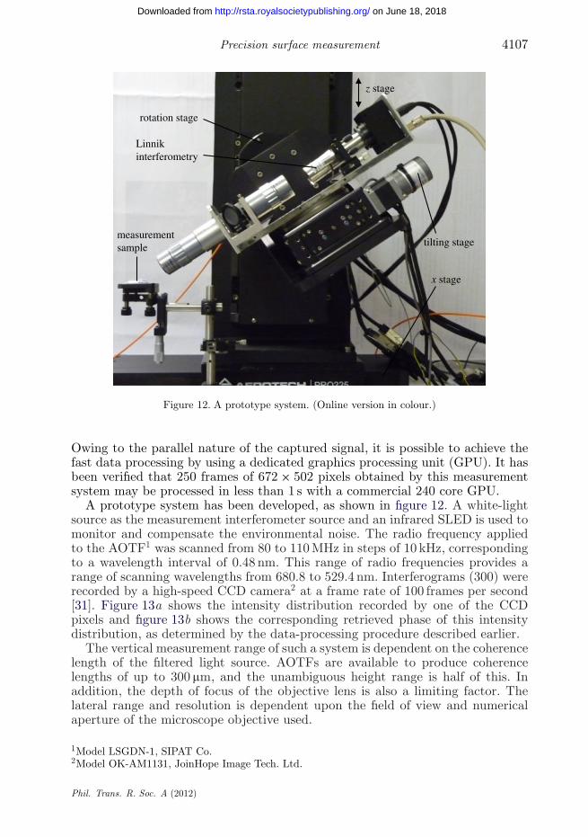
Owing to the parallel nature of the captured signal, it is possible to achieve thefast data processing by using a dedicated graphics processing unit (GPU). It hasbeen verified that 250 frames of 672 × 502 pixels obtained by this measurementsystem may be processed in less than 1 s with a commercial 240 core GPU.
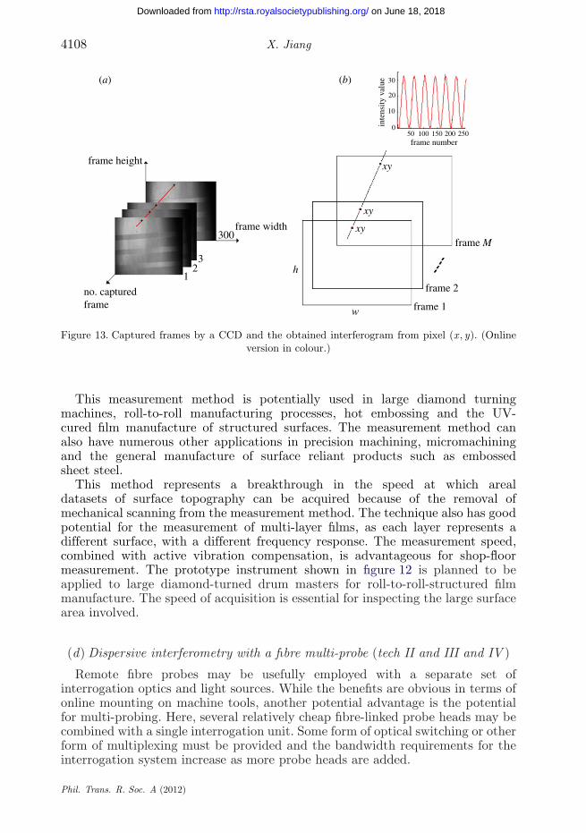
A prototype system has been developed, as shown in figure 12. A white-lightsource as the measurement interferometer source and an infrared SLED is used tomonitor and compensate the environmental noise. The radio frequency appliedto the AOTF1 was scanned from 80 to 110 MHz in steps of 10 kHz, correspondingto a wavelength interval of 0.48 nm. This range of radio frequencies provides arange of scanning wavelengths from 680.8 to 529.4 nm. Interferograms (300) wererecorded by a high-speed CCD camera2 at a frame rate of 100 frames per second[31]. Figure 13a shows the intensity distribution recorded by one of the CCDpixels and figure 13b shows the corresponding retrieved phase of this intensitydistribution, as determined by the data-processing procedure described earlier.
The vertical measurement range of such a system is dependent on the coherencelength of the filtered light source. AOTFs are available to produce coherencelengths of up to 300 mm, and the unambiguous height range is half of this. Inaddition, the depth of focus of the objective lens is also a limiting factor. Thelateral range and resolution is dependent upon the field of view and numericalaperture of the microscope objective used.
1Model LSGDN-1, SIPAT Co.2Model OK-AM1131, JoinHope Image Tech. Ltd.
Phil. Trans. R. Soc. A (2012)
on June 18, 2018http://rsta.royalsocietypublishing.org/Downloaded from
4108 X. Jiang
frame height
(a) (b)
inte
nsity
val
ue
frame number
frame M
frame 2
frame 1w
h
xy
xy
xy
500
10
20
30
100 150 200 250
no. capturedframe
frame width300
32
1
Figure 13. Captured frames by a CCD and the obtained interferogram from pixel (x , y). (Onlineversion in colour.)
This measurement method is potentially used in large diamond turningmachines, roll-to-roll manufacturing processes, hot embossing and the UV-cured film manufacture of structured surfaces. The measurement method canalso have numerous other applications in precision machining, micromachiningand the general manufacture of surface reliant products such as embossedsheet steel.
This method represents a breakthrough in the speed at which arealdatasets of surface topography can be acquired because of the removal ofmechanical scanning from the measurement method. The technique also has goodpotential for the measurement of multi-layer films, as each layer represents adifferent surface, with a different frequency response. The measurement speed,combined with active vibration compensation, is advantageous for shop-floormeasurement. The prototype instrument shown in figure 12 is planned to beapplied to large diamond-turned drum masters for roll-to-roll-structured filmmanufacture. The speed of acquisition is essential for inspecting the large surfacearea involved.
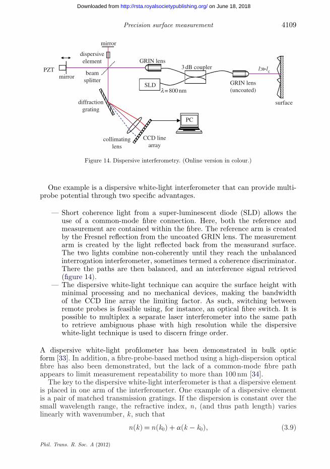
(d) Dispersive interferometry with a fibre multi-probe (tech II and III and IV )
Remote fibre probes may be usefully employed with a separate set ofinterrogation optics and light sources. While the benefits are obvious in terms ofonline mounting on machine tools, another potential advantage is the potentialfor multi-probing. Here, several relatively cheap fibre-linked probe heads may becombined with a single interrogation unit. Some form of optical switching or otherform of multiplexing must be provided and the bandwidth requirements for theinterrogation system increase as more probe heads are added.
Phil. Trans. R. Soc. A (2012)
on June 18, 2018http://rsta.royalsocietypublishing.org/Downloaded from
Precision surface measurement 4109
mirror
dispersiveelement
mirrorbeam
splitter
diffractiongrating
SLD
PC
GRIN lensl>>lc
GRIN lens(uncoated)
surface
PZT 3 dB coupler
CCD linearray
collimatinglens
l = 800 nm
Figure 14. Dispersive interferometry. (Online version in colour.)
One example is a dispersive white-light interferometer that can provide multi-probe potential through two specific advantages.
— Short coherence light from a super-luminescent diode (SLD) allows theuse of a common-mode fibre connection. Here, both the reference andmeasurement are contained within the fibre. The reference arm is createdby the Fresnel reflection from the uncoated GRIN lens. The measurementarm is created by the light reflected back from the measurand surface.The two lights combine non-coherently until they reach the unbalancedinterrogation interferometer, sometimes termed a coherence discriminator.There the paths are then balanced, and an interference signal retrieved(figure 14).
— The dispersive white-light technique can acquire the surface height withminimal processing and no mechanical devices, making the bandwidthof the CCD line array the limiting factor. As such, switching betweenremote probes is feasible using, for instance, an optical fibre switch. It ispossible to multiplex a separate laser interferometer into the same pathto retrieve ambiguous phase with high resolution while the dispersivewhite-light technique is used to discern fringe order.
A dispersive white-light profilometer has been demonstrated in bulk opticform [33]. In addition, a fibre-probe-based method using a high-dispersion opticalfibre has also been demonstrated, but the lack of a common-mode fibre pathappears to limit measurement repeatability to more than 100 nm [34].
The key to the dispersive white-light interferometer is that a dispersive elementis placed in one arm of the interferometer. One example of a dispersive elementis a pair of matched transmission gratings. If the dispersion is constant over thesmall wavelength range, the refractive index, n, (and thus path length) varieslinearly with wavenumber, k, such that
n(k) = n(k0) + a(k − k0), (3.9)
Phil. Trans. R. Soc. A (2012)
on June 18, 2018http://rsta.royalsocietypublishing.org/Downloaded from

4110 X. Jiang
8
6
4
2
0
1
0
kc
kc
kphas
e di
ffer
ence
(ra
d) (
p)no
rmal
ized
spec
tral
inte
nsity
wavenumber (k)k
(a)
(b)
Figure 15. (a) Phase difference and (b) intensity response as functions of wavenumber, k. (Onlineversion in colour.)
where k0 is the central wavenumber of the light source and a is the dispersionparameter. The result is that each component wavelength of the white-lightsource used to illuminate the device has a different path length and thus theinterferometer is balanced only at one point.
When the intensity from the interferometer is analysed spectrally, andneglecting any attenuation and polarization effects in each arm, the resultantresponse, I (k), is found to be
I (k) = A(k) + B(k) cos q(k). (3.10)
The phase q(k) is dependent on the optical path length and may be written withrespect to equation (3.9) as
q(k) = 2k{z − d[n(k0) + a(k − k0) − 1]}. (3.11)
The result of this is that a symmetric intensity pattern is formed with a definitecentral peak located at kc. The response of the phase difference with changingwavenumber is shown in figure 15a.
It can be seen from equation (3.11) that the peak of kc occurs only atan absolute distance, z0, that is determined by the length, d, and dispersioncoefficient, a, of the dispersive element. If the path length changes, then theposition with respect to wavenumber of the intensity peak also changes linearly.By determining the wavenumber at which the peak occurs, the new pathdifference z may thus be determined absolutely.
An advantage of this technique is that the measurement range is scaled by theamount of dispersion in the reference arm. Thus, the system may be operated witha range of a few nanometres to several hundred micrometres. The resolution is
Phil. Trans. R. Soc. A (2012)
on June 18, 2018http://rsta.royalsocietypublishing.org/Downloaded from
Precision surface measurement 4111
limited by the number of spectrometer pixels available and currently it can reach8192 pixels. Multi-probing potential with this technique also points towards away of reducing the cost of metrology by providing low-cost multiple probe headswith a single interrogation unit.
4. Conclusion
This study has addressed the problems and challenges in the subject areaof surface measurement for next-generation precision and ultra-precisionmanufacture, for example: (i) large-scale (up to metres) ultra-precision(nanometre tolerance) components with complex surfaces such as, telescopemirror segments; photovoltaic panels and large substrates, in which themeasurements do not allow removal from a machine tool/production line and(ii) precision surfaces with very small size that work in extreme environmentalconditions, such as fuel shells for inertial-confinement fusion. The next generationof measurement devices/instruments will require accessibility into manufacturingenvironments, online, non-contact and high-speed operation combined with easeof use, a small footprint and robustness. At the same time, they must match thesame level of measurement uncertainty as current state-of-the-art laboratory-based measurement systems, while also matching affordability in terms ofreducing manufacturing costs.
This study has discussed how rethinking some fundamental techniques,invented across several discipline areas, can create new measurement techniquesto provide a quick advance. In this study, five basic principles, multi-wavelength scanning interferometry, self-calibrating interferometry, wavelengthdivision multiplexing, wavelength absolute measurement and ‘Lab-on-a-chip’microsystems, have been briefly introduced. This has led to four types ofmeasurement systems that structurally combine these techniques in some fashion.This study has presented these techniques as having the potential to overcomecurrent measurement problems and challenges, and has shown their feasibility formanufacturing environment applications.
The research work and experimental studies in this study show thefollowing. (i) An optical-fibre-based surface interferometer with a remotemountable single-point wavelength scanning probe could provide a 9 mmscanning range over a profile in less than 1 s. It can reach sub-nanometrevertical resolution with 340–750 nm vertical ranges depending on the sourcewavelength. (ii) An integrated-optic chip interferometer that presents aminiaturized measurement system. Current experiments have shown that thisoptical chip has a laser tuning range of approximately 92 nm while maintaininggreater than 5 mW output power, 40 pm tuning resolution and less than1 s tuning period, all fully integrated into a single small package. Thesystem has two possible modes of operation. The first is using a wavelengthdivision multiplexed scanning probe head for profile measurement and thesecond is in a Fizeau-type configuration that can provide absolute distancemeasurement of a single point. (iii) A spectral scanning interferometer providesfull-field surface measurement for large manufacturing systems, with a 1 smeasurement period and sub-nanometre resolution over a 300 mm verticalrange. Furthermore, it has the capability for multi-layer thick- and thin-film
Phil. Trans. R. Soc. A (2012)
on June 18, 2018http://rsta.royalsocietypublishing.org/Downloaded from
4112 X. Jiang
measurements. (iv) A dispersive white-light interferometer providing single-point measurements with a compact fibre-linked probe. It can reach a 10 kHzmeasurement rate with nanometre resolution over a measurement range of severalhundred micrometres.
These measurement methods have the potential and feasibility formanufacturing environment applications. Some can be used online in largediamond turning machines, large substrate manufacturing processes, hotembossing and UV-cured film manufacture of structured surfaces. Others canbe used for numerous applications in precision machining, micro-machiningand the general manufacture of surface reliant products such as embossedsheet steel.
Beside the challenges in the instrumentation aspects being discussed throughthis study, looking forward, the integration of these measurement techniques intothe manufacturing environment will lead to further challenges, which include theestablishment of measurement coordinate systems in machine-tool environments,calibration methods and traceability for fast online measurement, and surfacecharacterization in conjunction with machine-tool error diagnostics andcompensation. The integration will also concern the creation of mechanical andcontrol solutions for device/instrument delivery, plus swarf and vaporized coolantremoval. In summary, if ultra-precision/precision/nanosurfaces are to be becomeeconomically viable in both science programmes and high add valued technology,all the earlier-cited challenges in measurement must be systemically solved inparallel with the evolution of the manufacturing process, to produce the enablingfuture envisioned.
X. Jiang gratefully acknowledges the Royal Society under a Wolfson Royal Society ResearchMerit Award, the European Research Council for its ‘Ideal Specific programme’ ERC-2008-AdG228117-Surfund and the UK Engineering and Physical Sciences Research Council (EPSRC) underits programme EP/E03733X/1 and manufacture future programmes. The author also gratefullyacknowledges the major contributor Dr Haydn Martin who went through the basic principles andexperimental studies, together with other researchers who have worked on this subject duringthe course: Dr Feng Gao, Dr Kaiwei Wang, Dr Dejiao Lin, Dr Shuming Yang and Mr HussamMuhammedsalih.
References
1 Jiang, X., Scott, P., Whitehouse, D. & Blunt, L. 2007 Paradigm shifts in surface metrology. II.The current shift. Proc. R. Soc. A 463, 2071–2099. (doi:10.1098/rspa.2007.1873)
2 Shore, P. & Burman, P. 2004 Manufacture of large mirrors for ELTs: a fresh perspective, opticalfabrication, testing, and metrology. Proc. SPIE 5252, 55–62. (doi:10.1117/12.514698)
3 Walker, N. 2010 Microoptics for low energy lighting applications. In Euspen specialinterest group meeting: structured and freeform surfaces, Aachen, Germany, 10–11February 2010.
4 RCUK Basic Technology: GRS85344/01. 2008 Ultra precision surfaces: a new paradigm(accuracy capability of 1 part 10 to the power of 8).
5 FP7-NMP. 2010 Information and communication technologies; nanosciences, nanotechnologies,materials and new production technologies.
6 Stephens, R. B., Olson, D., Huang, H. & Gibson, J. B. 2003 Complete surface mapping of ICFshells. General Atomics report GA-A24452.
7 FP7-NMP. 2011 Development of nano-scale detection and control techniques for large areasubstrates.
Phil. Trans. R. Soc. A (2012)
on June 18, 2018http://rsta.royalsocietypublishing.org/Downloaded from
Precision surface measurement 4113
8 ERC-AdG-228117. 2008 Fundaments and principles for measurement and characterization of21st century science and engineering surfaces.
9 Whitehouse, D. J. 2011 Handbook of surface and nanometrology. New York, NY: CRC Press.10 Taylor Hobson. 2011 Talysurf PGI 2540. See http://www.taylor-hobson.com/uploads/images/
talysurfpgi2540.pdf.11 Bauza, M. B., Woody, S. C., Smith, S. T. & Hocken, R. J. 2006 Development of a rapid
profilometer with an application to roundness gauging. Prec. Eng. 30, 406–413. (doi:10.1016/j.precisioneng.2005.12.001)
12 Muralikrishnan, B., Stone, J. A. & Stoup, J. R. 2006 Fiber deflection probe for small holemetrology. Prec. Eng. 30, 154–164. (doi:10.1016/j.precisioneng.2005.07.004)
13 Danzebrink, H.-U., Koenders, L., Wilkening, G., Yacoot, A. & Kunzmann, H. 2006 Advances inscanning force microscopy for dimensional metrology. Annu. CIRP 55, 841–864. (doi:10.1016/j.cirp.2006.10.010)
14 Hocken, R. J., Chakraborty, N. & Brown, C. 2005 Optical metrology of surfaces. Ann. CIRP54, 705–719. (doi:10.1016/S0007-8506(07)60025-0)
15 Bruker, A. X. S. 2011 NP flex brochure. See http://www.bruker-axs.com/uploads/tx_linkselectorforpdfpool/NPFLEX_3D_White_Light_Interferometric_Profilometer_brochure.pdf.
16 Hybl, O. & Hausler, G. 2010 Information efficient white-light interferometry. In ASPEsummer topical meeting on precision interferometric metrology, Asheville, NC, USA, 23–25June.
17 Creath, K. & Wyant, J. C. 1990 Absolute measurement of surface roughness. Appl. Opt. 29,3823–3827. (doi:10.1364/AO.29.003823)
18 Cheng, Y.-Y. & Wyant, J. C. 1984 Two-wavelength phase shifting interferometry. Appl. Opt.23, 4539–4543. (doi:10.1364/AO.23.004539)
19 Cheng, Y.-Y. & Wyant, J. C. 1985 Multiple-wavelength phase-shifting interferometry. Appl.Opt. 24, 804–807. (doi:10.1364/AO.24.000804)
20 Häusler, G., Richter, C., Leitz, K.-H. & Knauer, M. C. 2008 Microdeflectometry: a novel toolto acquire three-dimensional microtopography with nanometer height resolution. Opt. Lett. 33,396–398. (doi:10.1364/OL.33.000396)
21 Dupuy, M. O. 1967 High precision optical profilometer for the study of micro geometricalsurface defects, Archive: Proceedings of the Institution of Mechanical Engineers, ConferenceProceedings 1964–1970 (vols 178–184), Various titles labelled Volumes A to S 182(311),255–259.
22 Tiziani, H. J., Achi, R. & Krämer, R. 1996 Chromatic confocal microscopy with microlenses.J. Mod. Opt. 43, 155–163. (doi:10.1080/09500349608232730)
23 Drabarek, P. 2004 Short coherence fiber probe interferometric measuring device. Robert BoschGmbH. US 6741355 B2.
24 Martin, H. & Jiang, X. 2010 Rapid phase shifting fiber interferometer with optical stylus. Opt.Lett. 35, 655–657. (doi:10.1364/OL.35.000655)
25 Jackson, D., Priest, R., Dandridge, A. & Tveten, A. 1980 Elimination of drift in a single-mode optical fibre interferometer using a piezoelectrically stretched coiled fibre. Appl. Opt. 19,2926–2929. (doi:10.1364/AO.19.002926)
26 Annovazzi-Lodi, V., Donati, S. & Merlo, S. 1996 Thermodynamic phase noise in fibreinterferometers. Opt. Quant. Electron. 28, 43–49. (doi:10.1007/BF00578549)
27 Simon, A. & Ulrich, R. 1977 Evolution of polarisation along a single-mode fibre. App. Phys.Lett. 31, 517–520. (doi:10.1063/1.89760)
28 Martin, H., Wang, K. & Jiang, X. 2008 Vibration compensating beam scanning interferometerfor surface measurement. Appl. Opt. 47, 888–893. (doi:10.1364/AO.47.000888)
29 Jiang, X. & Whitehouse, D. J. 2006 A miniaturized optical measurement method for surfacenanometrology. Annal. CIRP 55, 577–580. (doi:10.1016/S0007-8506(07)60486-7)
30 Yang, S., Jiang, X., Maxwell, G., Wyatt, R. & Rogers, D. 2010 A chip tuneable laser developedfor on-line micro–nano scale surface measurements. Meas. Sci. Technol. 21, 105901 (doi:10.1088/0957-0233/21/10/105901)
Phil. Trans. R. Soc. A (2012)
on June 18, 2018http://rsta.royalsocietypublishing.org/Downloaded from
4114 X. Jiang
31 Jiang, X., Wang, K., Gao, F. & Muhamedsalih, H. 2010 Fast surface measurement usingwavelength scanning interferometry with compensation of environmental noise. Appl. Opt. 49,2903–2909. (doi:10.1364/AO.49.002903)
32 Hayes, J. 2002 Dynamic interferometry handles vibration. Laser Focus World 38,109–113.
33 Schwider, J. & Zhou, L. 1994 Dispersive interferometric profilometer. Opt. Lett. 19, 995–997.(doi:10.1364/OL.19.000995)
34 Pavlícek, P. & Häusler, G. 2005 White-light interferometer with dispersion: an accuratefiber-optic sensor for the measurement of distance. Appl. Opt. 44, 2978–2983. (doi:10.1364/AO.44.002978)
Phil. Trans. R. Soc. A (2012)
on June 18, 2018http://rsta.royalsocietypublishing.org/Downloaded from
Related Documents