Precision, Miniature MEMs IMU Data Sheet ADIS16475 Rev. A Document Feedback Information furnished by Analog Devices is believed to be accurate and reliable. However, no responsibility is assumed by Analog Devices for its use, nor for any infringements of patents or other rights of third parties that may result from its use. Specifications subject to change without notice. No license is granted by implication or otherwise under any patent or patent rights of Analog Devices. Trademarks and registered trademarks are the property of their respective owners. One Technology Way, P.O. Box 9106, Norwood, MA 02062-9106, U.S.A. Tel: 781.329.4700 ©2017 Analog Devices, Inc. All rights reserved. Technical Support www.analog.com FEATURES Triaxial, digital gyroscope ±125°/sec, ±500°/sec, ±2000°/sec range models 2°/hr in-run bias stability (ADIS16475-1) 0.15°/√hr angle random walk (ADIS16475-1 and ADIS16475-2) ±0.1° axis to axis misalignment error Triaxial, digital accelerometer, ±8 g 3.6 μg in-run bias stability Triaxial, delta angle and delta velocity outputs Factory calibrated sensitivity, bias, and axial alignment Calibration temperature range: −40°C to +85°C SPI compatible data communications Programmable operation and control Automatic and manual bias correction controls Data ready indicator for synchronous data acquisition External sync modes: direct, pulse, scaled, and output On demand self test of inertial sensors On demand self test of flash memory Single-supply operation (VDD): 3.0 V to 3.6 V 2000 g mechanical shock survivability Operating temperature range: −40°C to +105°C APPLICATIONS Navigation, stabilization, and instrumentation Unmanned and autonomous vehicles Smart agriculture and construction machinery Factory/industrial automation, robotics Virtual/augmented reality Internet of Moving Things GENERAL DESCRIPTION The ADIS16475 is a precision, miniature MEMS inertial measure- ment unit (IMU) that includes a triaxial gyroscope and a triaxial accelerometer. Each inertial sensor in the ADIS16475 combines with signal conditioning that optimizes dynamic performance. The factory calibration characterizes each sensor for sensitivity, bias, alignment, linear acceleration (gyroscope bias), and point of percussion (accelerometer location). As a result, each sensor has dynamic compensation formulas that provide accurate sensor measurements over a broad set of conditions. The ADIS16475 provides a simple, cost effective method for integrating accurate, multiaxis inertial sensing into industrial systems, especially when compared with the complexity and investment associated with discrete designs. All necessary motion testing and calibration are part of the production process at the factory, greatly reducing system integration time. Tight orthogonal alignment simplifies inertial frame alignment in navigation systems. The serial peripheral interface (SPI) and register structure provide a simple interface for data collection and configuration control. The ADIS16475 is available in a 44-ball, ball grid array (BGA) package that is approximately 11 mm × 15 mm × 11 mm. FUNCTIONAL BLOCK DIAGRAM CONTROLLER POWER MANAGEMENT CS SCLK DIN DOUT GND VDD DR SYNC RST SPI SELF TEST I/O OUTPUT DATA REGISTERS USER CONTROL REGISTERS CALIBRATION AND FILTERS ADIS16475 CLOCK 15436-001 TRIAXIAL GYROSCOPE TEMPERATURE SENSOR TRIAXIAL ACCELEROMETER Figure 1.

Welcome message from author
This document is posted to help you gain knowledge. Please leave a comment to let me know what you think about it! Share it to your friends and learn new things together.
Transcript

Precision, Miniature MEMs IMU Data Sheet ADIS16475
Rev. A Document Feedback Information furnished by Analog Devices is believed to be accurate and reliable. However, no responsibility is assumed by Analog Devices for its use, nor for any infringements of patents or other rights of third parties that may result from its use. Specifications subject to change without notice. No license is granted by implication or otherwise under any patent or patent rights of Analog Devices. Trademarks and registered trademarks are the property of their respective owners.
One Technology Way, P.O. Box 9106, Norwood, MA 02062-9106, U.S.A. Tel: 781.329.4700 ©2017 Analog Devices, Inc. All rights reserved. Technical Support www.analog.com
FEATURES Triaxial, digital gyroscope
±125°/sec, ±500°/sec, ±2000°/sec range models 2°/hr in-run bias stability (ADIS16475-1) 0.15°/√hr angle random walk (ADIS16475-1 and
ADIS16475-2) ±0.1° axis to axis misalignment error
Triaxial, digital accelerometer, ±8 g 3.6 μg in-run bias stability
Triaxial, delta angle and delta velocity outputs Factory calibrated sensitivity, bias, and axial alignment
Calibration temperature range: −40°C to +85°C SPI compatible data communications Programmable operation and control
Automatic and manual bias correction controls Data ready indicator for synchronous data acquisition External sync modes: direct, pulse, scaled, and output On demand self test of inertial sensors On demand self test of flash memory
Single-supply operation (VDD): 3.0 V to 3.6 V 2000 g mechanical shock survivability Operating temperature range: −40°C to +105°C
APPLICATIONS Navigation, stabilization, and instrumentation Unmanned and autonomous vehicles Smart agriculture and construction machinery Factory/industrial automation, robotics Virtual/augmented reality Internet of Moving Things
GENERAL DESCRIPTION The ADIS16475 is a precision, miniature MEMS inertial measure-ment unit (IMU) that includes a triaxial gyroscope and a triaxial accelerometer. Each inertial sensor in the ADIS16475 combines with signal conditioning that optimizes dynamic performance. The factory calibration characterizes each sensor for sensitivity, bias, alignment, linear acceleration (gyroscope bias), and point of percussion (accelerometer location). As a result, each sensor has dynamic compensation formulas that provide accurate sensor measurements over a broad set of conditions.
The ADIS16475 provides a simple, cost effective method for integrating accurate, multiaxis inertial sensing into industrial systems, especially when compared with the complexity and investment associated with discrete designs. All necessary motion testing and calibration are part of the production process at the factory, greatly reducing system integration time. Tight orthogonal alignment simplifies inertial frame alignment in navigation systems. The serial peripheral interface (SPI) and register structure provide a simple interface for data collection and configuration control.
The ADIS16475 is available in a 44-ball, ball grid array (BGA) package that is approximately 11 mm × 15 mm × 11 mm.
FUNCTIONAL BLOCK DIAGRAM
CONTROLLER
POWERMANAGEMENT
CS
SCLK
DIN
DOUT
GND
VDDDR
SYNC
RST
SPI
SELF TEST I/O
OUTPUTDATA
REGISTERS
USERCONTROL
REGISTERS
CALIBRATIONAND
FILTERS
ADIS16475
CLOCK
1543
6-00
1
TRIAXIALGYROSCOPE
TEMPERATURESENSOR
TRIAXIALACCELEROMETER
Figure 1.

ADIS16475 Data Sheet
Rev. A | Page 2 of 33
TABLE OF CONTENTS Features .............................................................................................. 1 Applications ....................................................................................... 1 General Description ......................................................................... 1 Functional Block Diagram .............................................................. 1 Specifications ..................................................................................... 3
Timing Specifications .................................................................. 5 Absolute Maximum Ratings ....................................................... 7 Thermal Resistance ...................................................................... 7 ESD Caution .................................................................................. 7
Pin Configuration and Function Descriptions ............................. 8 Typical Performance Characteristics ........................................... 10 Theory of Operation ...................................................................... 11
Introduction ................................................................................ 11 Inertial Sensor Signal Chain ..................................................... 11 Register Structure ....................................................................... 12 Serial Peripheral Interface (SPI) ............................................... 13 Data Ready (DR) ........................................................................ 13
Reading Sensor Data .................................................................. 14 Device Configuration ................................................................ 15
User Register Memory Map .......................................................... 16 User Register Defintions ................................................................ 18
Gyroscope Data .......................................................................... 18 Delta Angles ................................................................................ 21 Delta Velocity .............................................................................. 22 Calibration................................................................................... 24
Applications Information .............................................................. 30 Assembly and Handling Tips .................................................... 30 Power Supply Considerations ................................................... 31 Evaluation Tools ......................................................................... 31
Packaging and Ordering Information ......................................... 33 Outline Dimensions ................................................................... 33 Ordering Guide .......................................................................... 33
REVISION HISTORY 11/2017—Rev. 0 to Rev. A Changes to Table 1 ............................................................................ 3 Deleted Endnote 1, Table 1; Renumbered Sequentially .............. 4 Added Endnote 2, Table 1; Renumbered Sequentially ................ 4 10/2017—Revision 0: Initial Version

Data Sheet ADIS16475
Rev. A | Page 3 of 33
SPECIFICATIONS Case temperature (TC) = 25°C, VDD = 3.3 V, angular rate = 0°/sec, dynamic range = ±2000°/sec ± 1 g, unless otherwise noted.
Table 1. Parameter Test Conditions/Comments Min Typ Max Unit GYROSCOPES
Dynamic Range ADIS16475-1 ±125 °/sec ADIS16475-2 ±500 °/sec ADIS16475-3 ±2000 °/sec Sensitivity ADIS16475-1, 32-bit 10,485,760 LSB/°/sec ADIS16475-2, 32-bit 2,621,440 LSB/°/sec ADIS16475-3, 32-bit 655,360 LSB/°/sec
Error over Temperature −40°C ≤ TC ≤ +85°C, 1σ ±0.3 % Misalignment Error Axis to axis, −40°C ≤ TC ≤ +85°C, 1 σ ±0.1 Degrees Nonlinearity1 ADIS16475-1, full scale (FS) = 125°/sec 0.2 % FS ADIS16475-2, FS = 500°/sec 0.2 % FS ADIS16475-3, FS = 2000°/sec 0.25 % FS Bias
Repeatability2 −40°C ≤ TC ≤ +85°C, 1 σ 0.7 °/sec In-Run Bias Stability ADIS16475-1, 1 σ 2 °/hr ADIS16475-2, 1 σ 2.5 °/hr ADIS16475-3, 1 σ 7 °/hr Angular Random Walk ADIS16475-1, 1 σ 0.15 °/√hr ADIS16475-2, 1 σ 0.15 °/√hr ADIS16475-3, 1 σ 0.3 °/√hr Error over Temperature −40°C ≤ TC ≤ +85°C, 1 σ ±0.2 °/sec Linear Acceleration Effect Any direction, 1 σ 0.01 °/sec/g Vibration Rectified Error (VRE) Random vibration, 2 grms, 50 Hz to 2 kHz 0.0005 °/sec/g2 Output Noise ADIS16475-1, 1 σ, no filtering 0.07 °/sec rms ADIS16475-2, 1 σ, no filtering 0.08 °/sec rms ADIS16475-3, 1 σ, no filtering 0.17 °/sec rms Rate Noise Density ADIS16475-1, f = 10 Hz to 40 Hz 0.003 °/sec/√Hz rms ADIS16475-2, f = 10 Hz to 40 Hz 0.003 °/sec/√Hz rms ADIS16475-3, f = 10 Hz to 40 Hz 0.007 °/sec/√Hz rms
3 dB Bandwidth 550 Hz Sensor Resonant Frequency 66 kHz
ACCELEROMETERS3 Each axis Dynamic Range ±8 g Sensitivity 32-bit data format 262,144,000 LSB/g
Error over temperature −40°C ≤ TC ≤ +85°C, 1 σ ±0.1 % Misalignment Error Axis to axis, −40°C ≤ TC ≤ +85°C, 1 σ ±0.05 Degrees Nonlinearity Best fit straight line, ±2 g 0.25 % FS Best fit straight line, ±8 g, x-axis 0.5 % FS Best fit straight line, ±8 g, y-axis and z-axis 1.5 % FS Bias
In-Run Bias Stability 1 σ 3.6 μg Velocity Random Walk 1 σ 0.012 m/sec/√hr Error over Temperature −40°C ≤ TC ≤ +85°C, 1 σ ±1 mg Output Noise No filtering 0.6 mg rms Noise Density f = 10 Hz to 40 Hz, no filtering 23 μg/√Hz rms
3 dB Bandwidth 600 Hz Sensor Resonant Frequency Y-axis and z-axis 2.4 kHz X-axis 2.2 kHz
ADIS16475 Data Sheet
Rev. A | Page 4 of 33
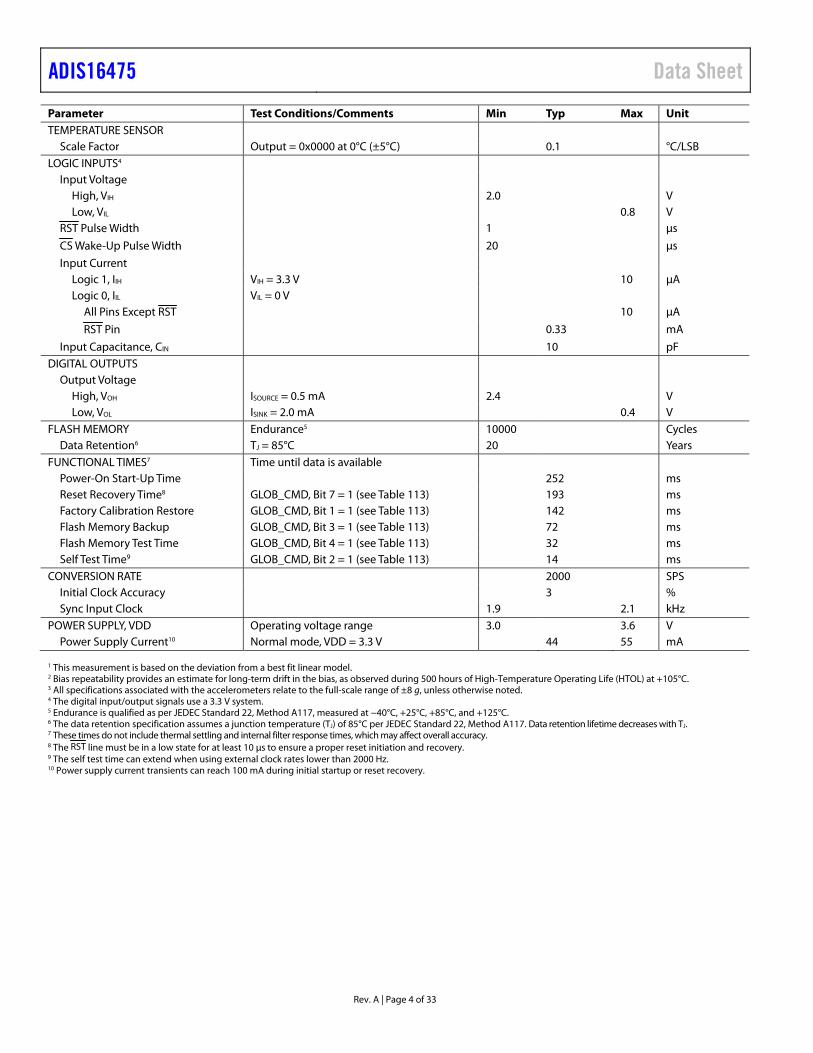
Parameter Test Conditions/Comments Min Typ Max Unit TEMPERATURE SENSOR
Scale Factor Output = 0x0000 at 0°C (±5°C) 0.1 °C/LSB LOGIC INPUTS4
Input Voltage High, VIH 2.0 V Low, VIL 0.8 V
RST Pulse Width 1 μs
CS Wake-Up Pulse Width 20 μs
Input Current Logic 1, IIH VIH = 3.3 V 10 μA Logic 0, IIL VIL = 0 V
All Pins Except RST 10 μA
RST Pin 0.33 mA
Input Capacitance, CIN 10 pF DIGITAL OUTPUTS
Output Voltage High, VOH ISOURCE = 0.5 mA 2.4 V Low, VOL ISINK = 2.0 mA 0.4 V
FLASH MEMORY Endurance5 10000 Cycles Data Retention6 TJ = 85°C 20 Years
FUNCTIONAL TIMES7 Time until data is available Power-On Start-Up Time 252 ms Reset Recovery Time8 GLOB_CMD, Bit 7 = 1 (see Table 113) 193 ms Factory Calibration Restore GLOB_CMD, Bit 1 = 1 (see Table 113) 142 ms Flash Memory Backup GLOB_CMD, Bit 3 = 1 (see Table 113) 72 ms Flash Memory Test Time GLOB_CMD, Bit 4 = 1 (see Table 113) 32 ms Self Test Time9 GLOB_CMD, Bit 2 = 1 (see Table 113) 14 ms
CONVERSION RATE 2000 SPS Initial Clock Accuracy 3 % Sync Input Clock 1.9 2.1 kHz
POWER SUPPLY, VDD Operating voltage range 3.0 3.6 V Power Supply Current10 Normal mode, VDD = 3.3 V 44 55 mA
1 This measurement is based on the deviation from a best fit linear model. 2 Bias repeatability provides an estimate for long-term drift in the bias, as observed during 500 hours of High-Temperature Operating Life (HTOL) at +105°C. 3 All specifications associated with the accelerometers relate to the full-scale range of ±8 g, unless otherwise noted. 4 The digital input/output signals use a 3.3 V system. 5 Endurance is qualified as per JEDEC Standard 22, Method A117, measured at −40°C, +25°C, +85°C, and +125°C. 6 The data retention specification assumes a junction temperature (TJ) of 85°C per JEDEC Standard 22, Method A117. Data retention lifetime decreases with TJ. 7 These times do not include thermal settling and internal filter response times, which may affect overall accuracy. 8 The RST line must be in a low state for at least 10 μs to ensure a proper reset initiation and recovery. 9 The self test time can extend when using external clock rates lower than 2000 Hz. 10 Power supply current transients can reach 100 mA during initial startup or reset recovery.
Data Sheet ADIS16475
Rev. A | Page 5 of 33
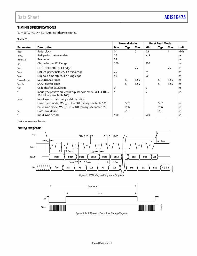
TIMING SPECIFICATIONS TA = 25°C, VDD = 3.3 V, unless otherwise noted.
Table 2.
Parameter Description Normal Mode Burst Read Mode
Unit Min Typ Max Min1 Typ Max fSCLK Serial clock 0.1 2 0.1 1 MHz tSTALL Stall period between data 16 N/A μs tREADRATE Read rate 24 μs tCS Chip select to SCLK edge 200 200 ns
tDAV DOUT valid after SCLK edge 25 25 ns tDSU DIN setup time before SCLK rising edge 25 25 ns tDHD DIN hold time after SCLK rising edge 50 50 ns tSCLKR, tSCLKF SCLK rise/fall times 5 12.5 5 12.5 ns tDR, tDF DOUT rise/fall times 5 12.5 5 12.5 ns tSFS CS high after SCLK edge 0 0 ns
t1 Input sync positive pulse width; pulse sync mode, MSC_CTRL = 101 (binary, see Table 105)
5 5 μs
tSTDR Input sync to data ready valid transition Direct sync mode, MSC_CTRL = 001 (binary, see Table 105) 507 507 μs Pulse sync mode, MSC_CTRL = 101 (binary, see Table 105) 256 256 μs tNV Data invalid time 20 20 μs t2 Input sync period 500 500 μs 1 N/A means not applicable.
Timing Diagrams
CS
SCLK
DOUT
DIN
1 2 3 4 5 6 15 16
R/W A5A6 A4 A3 A2 D2
MSB DB14
D1 LSB
DB13 DB12 DB10DB11 DB2 LSBDB1
tCS
tDR
tSFS
tDF
tDAV
tSCLKR tSCLKF
tDHDtDSU
154
36-0
02
Figure 2. SPI Timing and Sequence Diagram
CS
SCLK
tSTALL
tREADRATE
15
436
-00
3
Figure 3. Stall Time and Data Rate Timing Diagram

ADIS16475 Data Sheet
Rev. A | Page 6 of 33
SYNC
DR
t1
t2
tNV
tSTDR
1543
6-00
4
Figure 4. Input Clock Timing Diagram, Pulse Sync Mode, Register MSC_CTRL, Bits[4:2] = 101 (Binary)
SYNC
DR
t2
tNV
t1
tSTDR
1543
6-00
5
Figure 5. Input Clock Timing Diagram, Direct Sync Mode, Register MSC_CTRL, Bits[4:2] = 001 (Binary)
Data Sheet ADIS16475
Rev. A | Page 7 of 33
ABSOLUTE MAXIMUM RATINGS
Table 3. Parameter Rating Mechanical Shock Survivability
Any Axis, Unpowered 2000 g Any Axis, Powered 2000 g
VDD to GND −0.3 V to +3.6 V Digital Input Voltage to GND −0.3 V to VDD + 0.2 V Digital Output Voltage to GND −0.3 V to VDD + 0.2 V Calibration Temperature Range −40°C to +85°C Operating Temperature Range −40°C to +105°C Storage Temperature Range1 −65°C to +150°C
Barometric Pressure 2 bar
1 Extended exposure to temperatures that are lower than −20°C or higher than +85°C can adversely affect the accuracy of the factory calibration.
Stresses at or above those listed under Absolute Maximum Ratings may cause permanent damage to the product. This is a stress rating only; functional operation of the product at these or any other conditions above those indicated in the operational section of this specification is not implied. Operation beyond the maximum operating conditions for extended periods may affect product reliability.
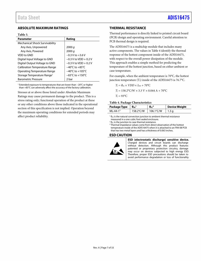
THERMAL RESISTANCE Thermal performance is directly linked to printed circuit board (PCB) design and operating environment. Careful attention to PCB thermal design is required.
The ADIS16475 is a multichip module that includes many active components. The values in Table 4 identify the thermal response of the hottest component inside of the ADIS16475, with respect to the overall power dissipation of the module. This approach enables a simple method for predicting the temperature of the hottest junction, based on either ambient or case temperature.
For example, when the ambient temperature is 70°C, the hottest junction temperature (TJ) inside of the ADIS16475 is 76.7°C.
TJ = θJA × VDD × IDD + 70°C
TJ = 158.2°C/W × 3.3 V × 0.044 A + 70°C
TJ = 93°C
Table 4. Package Characteristics Package Type θJA
1 θJC2 Device Weight
ML-44-13 158.2°C/W 106.1°C/W 1.3 g
1 θJA is the natural convection junction to ambient thermal resistance measured in a one cubic foot sealed enclosure.
2 θJC is the junction to case thermal resistance. 3 Thermal impedance values come from direct observation of the hottest
temperature inside of the ADIS16475 when it is attached to an FR4-08 PCB that has two metal layers and has a thickness of 0.063 inches.
ESD CAUTION

ADIS16475 Data Sheet
Rev. A | Page 8 of 33
PIN CONFIGURATION AND FUNCTION DESCRIPTIONS A
1
B C D E F G H J
2
3
4
5
6
7
8
K
1543
6-00
6
BOTTOM VIEW OF PACKAGE
ADIS16475
Figure 6. Pin Assignments, Bottom View
PIN A8
PIN A1
PIN K8 1543
6-00
7
Figure 7. Pin Assignments, Package Level View
Table 5. Pin Function Descriptions Pin No. Mnemonic Type Description A1 GND Supply Power Ground A2 GND Supply Power Ground A3 GND Supply Power Ground A4 GND Supply Power Ground A5 GND Supply Power Ground A6 GND Supply Power Ground A7 GND Supply Power Ground A8 GND Supply Power Ground B3 GND Supply Power Ground B4 GND Supply Power Ground B5 GND Supply Power Ground B6 GND Supply Power Ground C2 GND Supply Power Ground C3 DNC Not applicable Do Not Connect C6 GND Supply Power Ground C7 VDD Supply Power Supply D3 GND Supply Power Ground D6 VDD Supply Power Supply E2 GND Supply Power Ground E3 VDD Supply Power Supply E6 GND Supply Power Ground E7 GND Supply Power Ground F1 GND Supply Power Ground F3 RST Input Reset
F6 GND Supply Power Ground F8 GND Supply Power Ground G2 GND Supply Power Ground G3 CS Input SPI, Chip Select
G6 DIN Input SPI, Data Input G7 GND Supply Power Supply H1 VDD Supply Power Supply H3 DOUT Output SPI, Data Output H6 SCLK Input SPI, Serial Clock H8 GND Supply Power Ground

Data Sheet ADIS16475
Rev. A | Page 9 of 33
Pin No. Mnemonic Type Description J2 GND Supply Power Ground J3 SYNC Input Sync (External Clock) J4 VDD Supply Power Supply J5 VDD Supply Power Supply J6 DR Output Data Ready J7 GND Supply Power Ground K1 GND Supply Power Ground K3 GND Supply Power Ground K6 VDD Supply Power Supply K8 GND Supply Power Ground
ADIS16475 Data Sheet
Rev. A | Page 10 of 33
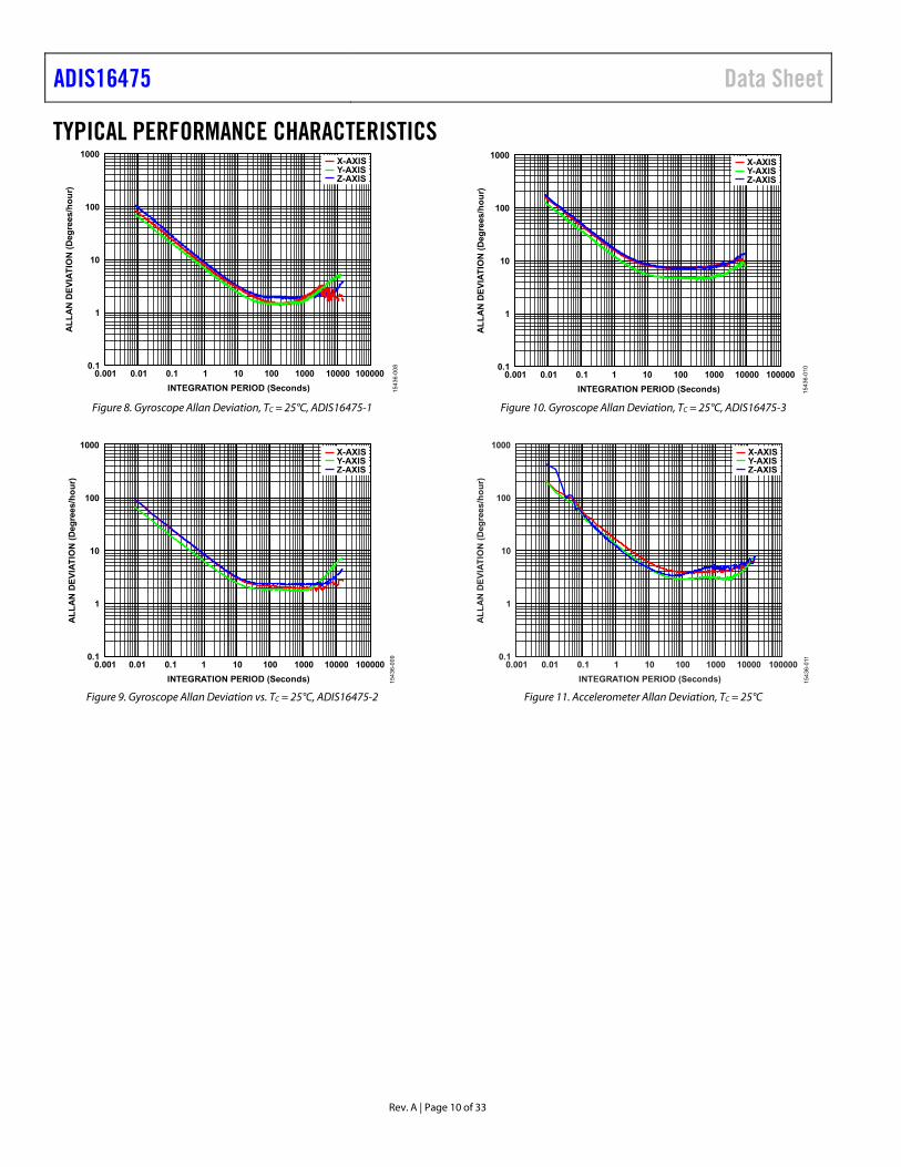
TYPICAL PERFORMANCE CHARACTERISTICS
0.001 0.01 0.1 1 10 100 1000 10000 100000INTEGRATION PERIOD (Seconds)
0.1
1
10
100
1000
ALL
AN
DEV
IATI
ON
(Deg
rees
/hou
r)
X-AXISY-AXISZ-AXIS
1543
6-00
8
Figure 8. Gyroscope Allan Deviation, TC = 25°C, ADIS16475-1
0.001 0.01 0.1 1 10 100 1000 10000 100000INTEGRATION PERIOD (Seconds)
0.1
1
10
100
1000
ALL
AN
DEV
IATI
ON
(Deg
rees
/hou
r)
X-AXISY-AXISZ-AXIS
1543
6-00
9
Figure 9. Gyroscope Allan Deviation vs. TC = 25°C, ADIS16475-2
0.001 0.01 0.1 1 10 100 1000 10000 100000INTEGRATION PERIOD (Seconds)
0.1
1
10
100
1000
ALL
AN
DEV
IATI
ON
(Deg
rees
/hou
r)
X-AXISY-AXISZ-AXIS
1543
6-01
0
Figure 10. Gyroscope Allan Deviation, TC = 25°C, ADIS16475-3
0.001 0.01 0.1 1 10 100 1000 10000 100000INTEGRATION PERIOD (Seconds)
0.1
1
10
100
1000
ALL
AN
DEV
IATI
ON
(Deg
rees
/hou
r)
X-AXISY-AXISZ-AXIS
1543
6-01
1
Figure 11. Accelerometer Allan Deviation, TC = 25°C
Data Sheet ADIS16475
Rev. A | Page 11 of 33
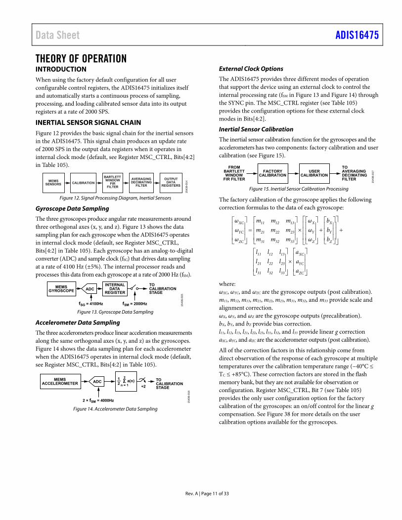
THEORY OF OPERATION INTRODUCTION When using the factory default configuration for all user configurable control registers, the ADIS16475 initializes itself and automatically starts a continuous process of sampling, processing, and loading calibrated sensor data into its output registers at a rate of 2000 SPS.
INERTIAL SENSOR SIGNAL CHAIN Figure 12 provides the basic signal chain for the inertial sensors in the ADIS16475. This signal chain produces an update rate of 2000 SPS in the output data registers when it operates in internal clock mode (default, see Register MSC_CTRL, Bits[4:2] in Table 105).
OUTPUTDATA
REGISTERS
AVERAGINGDECIMATING
FILTERCALIBRATION
BARTLETTWINDOW
FIRFILTER
MEMSSENSORS
154
36-0
14
Figure 12. Signal Processing Diagram, Inertial Sensors
Gyroscope Data Sampling
The three gyroscopes produce angular rate measurements around three orthogonal axes (x, y, and z). Figure 13 shows the data sampling plan for each gyroscope when the ADIS16475 operates in internal clock mode (default, see Register MSC_CTRL, Bits[4:2] in Table 105). Each gyroscope has an analog-to-digital converter (ADC) and sample clock (fSG) that drives data sampling at a rate of 4100 Hz (±5%). The internal processor reads and processes this data from each gyroscope at a rate of 2000 Hz (fSM).
MEMSGYROSCOPE
fSM = 2000Hz
INTERNALDATA
REGISTER
TOCALIBRATIONSTAGE
fSG = 4100Hz
ADC
1543
6-0
15
Figure 13. Gyroscope Data Sampling
Accelerometer Data Sampling
The three accelerometers produce linear acceleration measurements along the same orthogonal axes (x, y, and z) as the gyroscopes. Figure 14 shows the data sampling plan for each accelerometer when the ADIS16475 operates in internal clock mode (default, see Register MSC_CTRL, Bits[4:2] in Table 105).
MEMSACCELEROMETER
2 × fSM = 4000Hz
ADC TOCALIBRATIONSTAGE
12
2
n = 1a(n)
÷2
1543
6-0
16
Figure 14. Accelerometer Data Sampling
External Clock Options
The ADIS16475 provides three different modes of operation that support the device using an external clock to control the internal processing rate (fSM in Figure 13 and Figure 14) through the SYNC pin. The MSC_CTRL register (see Table 105) provides the configuration options for these external clock modes in Bits[4:2].
Inertial Sensor Calibration
The inertial sensor calibration function for the gyroscopes and the accelerometers has two components: factory calibration and user calibration (see Figure 15).
TOAVERAGINGDECIMATINGFILTER
FACTORYCALIBRATION
USERCALIBRATION
FROMBARTLETTWINDOW
FIR FILTER
154
36-0
17
Figure 15. Inertial Sensor Calibration Processing
The factory calibration of the gyroscope applies the following correction formulas to the data of each gyroscope:
ZC
YC
XC
333231
232221
131211
Z
Y
X
Z
Y
X
333231
232221
131211
ZC
YC
XC
aaa
lllllllll
bbb
ωωω
mmmmmmmmm
ωωω
where: ωXC, ωYC, and ωZC are the gyroscope outputs (post calibration). m11, m12, m13, m21, m22, m23, m31, m32, and m33 provide scale and alignment correction. ωX, ωY, and ωZ are the gyroscope outputs (precalibration). bX, bY, and bZ provide bias correction. l11, l12, l13, l21, l22, l23, l31, l32, and l33 provide linear g correction aXC, aYC, and aZC are the accelerometer outputs (post calibration).
All of the correction factors in this relationship come from direct observation of the response of each gyroscope at multiple temperatures over the calibration temperature range (−40°C ≤ TC ≤ +85°C). These correction factors are stored in the flash memory bank, but they are not available for observation or configuration. Register MSC_CTRL, Bit 7 (see Table 105) provides the only user configuration option for the factory calibration of the gyroscopes: an on/off control for the linear g compensation. See Figure 38 for more details on the user calibration options available for the gyroscopes.
ADIS16475 Data Sheet
Rev. A | Page 12 of 33
The factory calibration of the accelerometer applies the following correction formulas to the data of each accelerometer:
2
2
2
3231
2321
1312
333231
232221
131211
00
0
ZC
YC
XC
Z
Y
X
Z
Y
X
ZC
YC
XC
pppppp
bbb
aaa
mmmmmmmmm
aaa
where: aXC, aYC, and aZC are the accelerometer outputs (post calibration). m11, m12, m13, m21, m22, m23, m31, m32, and m33 provide scale and alignment correction. aX, aY, and aZ are the accelerometer outputs (precalibration). bX, bY, and bZ provide bias correction. p12, p13, p21, p23, p31, and p32 provide a point of percussion alignment correction (see Figure 41). ω2
XC, ω2YC, and ω2
ZC are the square of the gyroscope outputs (post calibration).
All of the correction factors in this relationship come from direct observation of the response of each accelerometer at multiple temperatures over the calibration temperature range (−40°C ≤ TC ≤ +85°C). These correction factors are stored in the flash memory bank, but they are not available for observation or configuration. MSC_CTRL, Bit 6 (see Table 105) provides the only user configuration option for the factory calibration of the accelerometers: an on/off control for the point of percussion, alignment function. See Figure 39 for more details on the user calibration options available for the accelerometers.
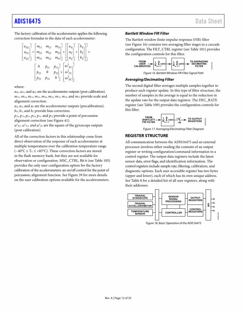
Bartlett Window FIR Filter
The Bartlett window finite impulse response (FIR) filter (see Figure 16) contains two averaging filter stages in a cascade configuration. The FILT_CTRL register (see Table 101) provides the configuration controls for this filter.
FROMUSER
CALIBRATION
TO AVERAGINGDECIMATING
FILTER
1N
N
n = 1ω(n)1
N
N
n = 1ω(n)
154
36-
018
Figure 16. Bartlett Window FIR Filter Signal Path
Averaging/Decimating Filter
The second digital filter averages multiple samples together to produce each register update. In this type of filter structure, the number of samples in the average is equal to the reduction in the update rate for the output data registers. The DEC_RATE register (see Table 109) provides the configuration controls for this filter.
FROMBARTLETTFIR FILTER ÷N
TO OUTPUTREGISTERSΣ1
N
N
n = 1ω(n)
154
36-
019
Figure 17. Averaging/Decimating Filter Diagram
REGISTER STRUCTURE All communication between the ADIS16475 and an external processor involves either reading the contents of an output register or writing configuration/command information to a control register. The output data registers include the latest sensor data, error flags, and identification information. The control registers include sample rate, filtering, calibration, and diagnostic options. Each user accessible register has two bytes (upper and lower), each of which has its own unique address. See Table 8 for a detailed list of all user registers, along with their addresses.
TRIAXIALGYROSCOPE
TEMPERATURESENSOR
TRIAXIALACCELLEROMETER
OUTPUTREGISTERS
CONTROLREGISTERSCONTROLLER
SENSORSIGNAL
PROCESSING
SP
I
1543
6-0
20
Figure 18. Basic Operation of the ADIS16475

Data Sheet ADIS16475
Rev. A | Page 13 of 33
SERIAL PERIPHERAL INTERFACE (SPI) The SPI provides access to the user registers (see Table 8). Figure 19 shows the most common connections between the ADIS16475 and a SPI master device, which is often an embedded processor that has a SPI-compatible interface. In this example, the SPI master uses an interrupt service routine to collect data every time the data ready (DR) signal pulses.
CS
SYSTEMPROCESSORSPI MASTER
VDD
I/O LINES ARE COMPATIBLE WITH3.3V LOGIC LEVELS
SCLK
DIN
DR
DOUT
SS
SCLK
MOSI
IRQ
MISO
ADIS16475
+3.3V
1543
6-02
1
Figure 19. Electrical Connection Diagram
Table 6. Generic SPI Master Pin Names and Functions Mnemonic Function SS Slave select
SCLK Serial clock MOSI Master output, slave input MISO Master input, slave output IRQ Interrupt request
Embedded processors typically use control registers to configure their serial ports for communicating with SPI slave devices such as the ADIS16475. Table 7 provides a list of settings that describe the SPI protocol of the ADIS16475. The initialization routine of the master processor typically establishes these settings using firmware commands to write them into the control registers.
Table 7. Generic Master Processor SPI Settings Processor Setting Description Master ADIS16475 operates as slave SCLK ≤ 2 MHz1 Maximum serial clock rate SPI Mode 3 CPOL = 1 (polarity), CPHA = 1 (phase) MSB First Mode Bit sequence, see Figure 24 for coding 16-Bit Mode Shift register and data length
1 A burst mode read requires this value to be ≤1 MHz (see Table 2 for more information).
DATA READY (DR) The factory default configuration provides users with a DR signal on the DR pin (see Table 5), which pulses when the output data registers are updating. Connect the DR pin to a pin on the embedded processor, which triggers data collection, on the second edge of this pulse. The MSC_CTRL register, Bit 0 (see Table 105), controls the polarity of this signal. In Figure 20, Register MSC_ CTRL, Bit 0 = 1, which means that data collection must start on the rising edges of the DR pulses.
DRACTIVE INACTIVE
1543
6-02
2
Figure 20. Data Ready When Register MSC_CTRL, Bit 0 = 1 (Default)
During the start-up and reset recovery processes, the DR signal may exhibit some transient behavior before data production begins. Figure 21 shows an example of the DR behavior during startup, and Figure 22 and Figure 23 provide examples of the DR behavior during recovery from reset commands.
VDD
DR
START-UP TIME
TIME THAT VDD > 3V
PULSING INDICATESDATA PRODUCTION
1543
6-02
3
Figure 21. Data Ready Response During Startup
DR
RESET RECOVERY TIME
SOFTWARE RESET COMMANDGLOB_CMD[7] = 1
DR PULSINGRESUMES
1543
6-02
4
Figure 22. Data Ready Response During Reset
(Register GLOB_CMD, Bit 7 = 1) Recovery
DR
RST
RESET RECOVERY TIME
RST PINRELEASED
DR PULSINGRESUMES
1543
6-02
5
Figure 23. Data Ready Response During Reset (RST = 0) Recovery
ADIS16475 Data Sheet
Rev. A | Page 14 of 33
R/W R/WA6 A5 A4 A3 A2 A1 A0 DC7 DC6 DC5 DC4 DC3 DC2 DC1 DC0
D0D1D2D3D4D5D6D7D8D9D10D11D12D13D14D15
CS
SCLK
DIN
DOUT
A6 A5
D13D14D15
NOTES1. DOUT BITS ARE PRODUCED ONLY WHEN THE PREVIOUS 16-BIT DIN SEQUENCE STARTS WITH R/W = 0.2. WHEN CS IS HIGH, DOUT IS IN A THREE-STATE, HIGH IMPEDANCE MODE, WHICH ALLOWS MULTIFUNCTIONAL USE OF THE LINE
FOR OTHER DEVICES. 1543
6-02
6
Figure 24. SPI Communication Bit Sequence
CS 1 2 3 11
SCLK
DIN
DOUT
0x6800
DIAG_STAT XGYRO_OUT CHECKSUM
1543
6-02
7
Figure 25. Burst Read Sequence
CS
SCLK
DIN
DOUT
DIN = 0x7200 = 0111 0010 0000 0000
DOUT = 0100 0000 0101 1011 = 0x405B = 16475 (PROD_ID) 1543
6-02
8
Figure 26. SPI Signal Pattern, Repeating Read of the PROD_ID Register
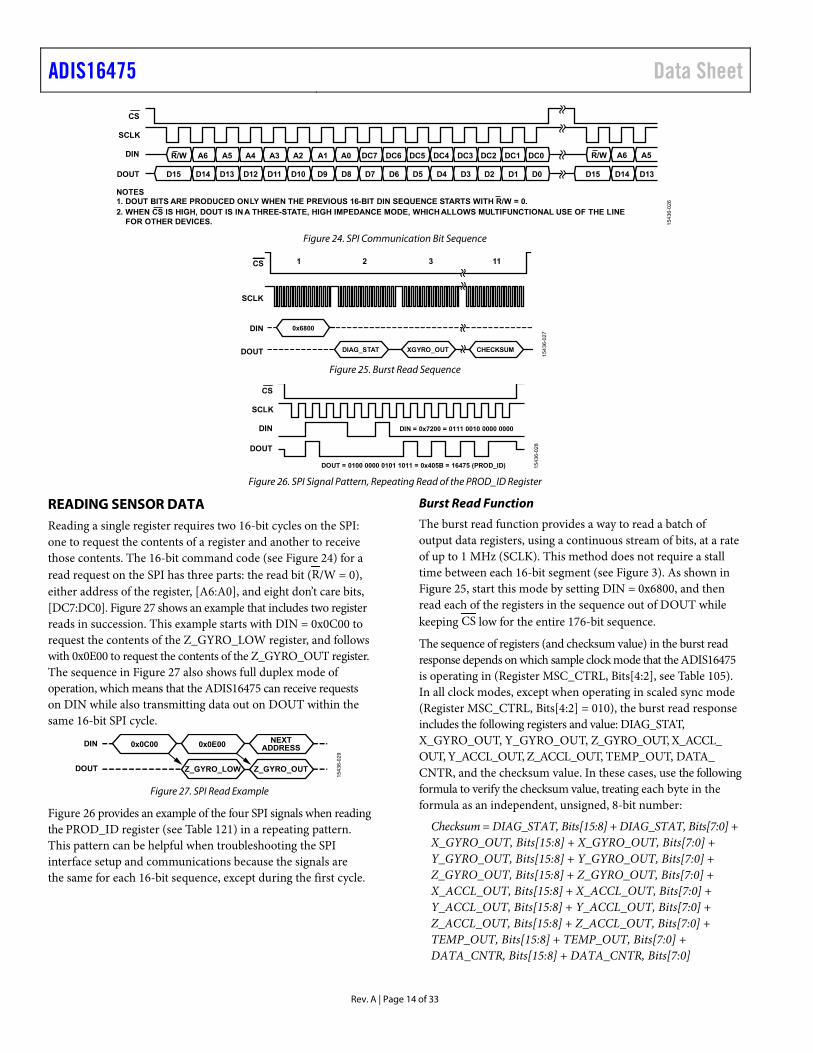
READING SENSOR DATA Reading a single register requires two 16-bit cycles on the SPI: one to request the contents of a register and another to receive those contents. The 16-bit command code (see Figure 24) for a read request on the SPI has three parts: the read bit (R/W = 0), either address of the register, [A6:A0], and eight don’t care bits, [DC7:DC0]. Figure 27 shows an example that includes two register reads in succession. This example starts with DIN = 0x0C00 to request the contents of the Z_GYRO_LOW register, and follows with 0x0E00 to request the contents of the Z_GYRO_OUT register. The sequence in Figure 27 also shows full duplex mode of operation, which means that the ADIS16475 can receive requests on DIN while also transmitting data out on DOUT within the same 16-bit SPI cycle.
DIN
DOUT
0x0C00 0x0E00 NEXTADDRESS
Z_GYRO_LOW Z_GYRO_OUT
1543
6-02
9
Figure 27. SPI Read Example
Figure 26 provides an example of the four SPI signals when reading the PROD_ID register (see Table 121) in a repeating pattern. This pattern can be helpful when troubleshooting the SPI interface setup and communications because the signals are the same for each 16-bit sequence, except during the first cycle.
Burst Read Function
The burst read function provides a way to read a batch of output data registers, using a continuous stream of bits, at a rate of up to 1 MHz (SCLK). This method does not require a stall time between each 16-bit segment (see Figure 3). As shown in Figure 25, start this mode by setting DIN = 0x6800, and then read each of the registers in the sequence out of DOUT while keeping CS low for the entire 176-bit sequence.
The sequence of registers (and checksum value) in the burst read response depends on which sample clock mode that the ADIS16475 is operating in (Register MSC_CTRL, Bits[4:2], see Table 105). In all clock modes, except when operating in scaled sync mode (Register MSC_CTRL, Bits[4:2] = 010), the burst read response includes the following registers and value: DIAG_STAT, X_GYRO_OUT, Y_GYRO_OUT, Z_GYRO_OUT, X_ACCL_ OUT, Y_ACCL_OUT, Z_ACCL_OUT, TEMP_OUT, DATA_ CNTR, and the checksum value. In these cases, use the following formula to verify the checksum value, treating each byte in the formula as an independent, unsigned, 8-bit number:
Checksum = DIAG_STAT, Bits[15:8] + DIAG_STAT, Bits[7:0] + X_GYRO_OUT, Bits[15:8] + X_GYRO_OUT, Bits[7:0] + Y_GYRO_OUT, Bits[15:8] + Y_GYRO_OUT, Bits[7:0] + Z_GYRO_OUT, Bits[15:8] + Z_GYRO_OUT, Bits[7:0] + X_ACCL_OUT, Bits[15:8] + X_ACCL_OUT, Bits[7:0] + Y_ACCL_OUT, Bits[15:8] + Y_ACCL_OUT, Bits[7:0] + Z_ACCL_OUT, Bits[15:8] + Z_ACCL_OUT, Bits[7:0] + TEMP_OUT, Bits[15:8] + TEMP_OUT, Bits[7:0] + DATA_CNTR, Bits[15:8] + DATA_CNTR, Bits[7:0]

Data Sheet ADIS16475
Rev. A | Page 15 of 33
When operating in scaled sync mode (Register MSC_CTRL, Bits[4:2] = 010), the burst read response includes the following registers and value: DIAG_STAT, X_GYRO_OUT, Y_GYRO_OUT, Z_GYRO_OUT, X_ACCL_OUT, Y_ACCL_OUT, Z_ACCL_OUT, TEMP_OUT, TIME_STAMP, and the checksum value. In this case, use the following formula to verify the checksum value, treating each byte in the formula as an independent, unsigned, 8-bit number.
Checksum = DIAG_STAT, Bits[15:8] + DIAG_STAT, Bits[7:0] + X_GYRO_OUT, Bits[15:8] + X_GYRO_OUT, Bits[7:0] + Y_GYRO_OUT, Bits[15:8] + Y_GYRO_OUT, Bits[7:0] + Z_GYRO_OUT, Bits[15:8] + Z_GYRO_OUT, Bits[7:0] + X_ACCL_OUT, Bits[15:8] + X_ACCL_OUT, Bits[7:0] + Y_ACCL_OUT, Bits[15:8] + Y_ACCL_OUT, Bits[7:0] + Z_ACCL_OUT, Bits[15:8] + Z_ACCL_OUT, Bits[7:0] + TEMP_OUT, Bits[15:8] + TEMP_OUT, Bits[7:0] + TIME_STAMP, Bits[15:8] + TIME_STAMP, Bits[7:0]
DEVICE CONFIGURATION Each configuration register contains 16 bits (two bytes). Bits[7:0] contain the low byte, and Bits[15:8] contain the high byte of each register. Each byte has its own unique address in the user register map (see Table 8). Updating the contents of a register requires writing to both of its bytes in the following sequence: low byte first, high byte second. There are three parts to coding a SPI command (see Figure 24) that write a new byte of data to a register: the write bit (R/W = 1), the address of the byte, [A6:A0], and the new data for that location, [DC7:DC0]. Figure 28 shows a coding example for writing 0x0004 to the FILT_CTRL register (see Table 101). In Figure 28, the 0xDC04 command writes 0x04 to Address 0x5C (lower byte) and the 0xDD00 command writes 0x00 to Address 0x5D (upper byte).
CS
SCLK
DIN 0xDC04 0xDD00
1543
6-03
0
Figure 28. SPI Sequence for Writing 0x0004 to FILT_CTRL
Memory Structure
Figure 29 provides a functional diagram for the memory structure of the ADIS16475. The flash memory bank contains the operational code, unit specific calibration coefficients, and user configuration settings. During initialization (power application or reset recover), this information loads from the flash memory into the static random access memory (SRAM), which supports all normal operation, including register access through the SPI port. Writing to a configuration register using the SPI updates the SRAM location of the register, but does not automatically update its settings in the flash memory bank. The manual flash memory update command (Register GLOB_CMD, Bit 3, see Table 113) provides a convenient method for saving all of these settings to the flash memory bank at one time. A yes in the flash backup column of Table 8 identifies the registers that have storage support in the flash memory bank.
NONVOLATILEFLASH MEMORY
(NO SPI ACCESS)
MANUALFLASH
BACKUP
START-UPRESET
VOLATILESRAM
SPI ACCESS
1543
6-03
1
Figure 29. SRAM and Flash Memory Diagram

ADIS16475 Data Sheet
Rev. A | Page 16 of 33
USER REGISTER MEMORY MAP Table 8. User Register Memory Map (N/A Means Not Applicable) Name R/W Flash Backup Address Default Register Description Reserved N/A N/A 0x00, 0x01 N/A Reserved DIAG_STAT R No 0x02, 0x03 0x0000 Output, system error flags X_GYRO_LOW R No 0x04, 0x05 N/A Output, x-axis gyroscope, low word X_GYRO_OUT R No 0x06, 0x07 N/A Output, x-axis gyroscope, high word Y_GYRO_LOW R No 0x08, 0x09 N/A Output, y-axis gyroscope, low word Y_GYRO_OUT R No 0x0A, 0x0B N/A Output, y-axis gyroscope, high word Z_GYRO_LOW R No 0x0C, 0x0D N/A Output, z-axis gyroscope, low word Z_GYRO_OUT R No 0x0E, 0x0F N/A Output, z-axis gyroscope, high word X_ACCL_LOW R No 0x10, 0x11 N/A Output, x-axis accelerometer, low word X_ACCL_OUT R No 0x12, 0x13 N/A Output, x-axis accelerometer, high word Y_ACCL_LOW R No 0x14, 0x15 N/A Output, y-axis accelerometer, low word Y_ACCL_OUT R No 0x16, 0x17 N/A Output, y-axis accelerometer, high word Z_ACCL_LOW R No 0x18, 0x19 N/A Output, z-axis accelerometer, low word Z_ACCL_OUT R No 0x1A, 0x1B N/A Output, z-axis accelerometer, high word TEMP_OUT R No 0x1C, 0x1D N/A Output, temperature TIME_STAMP R No 0x1E, 0x1F N/A Output, time stamp Reserved N/A N/A 0x20, 0x21 N/A Reserved DATA_CNTR R No 0x22, 0x23 N/A New data counter X_DELTANG_LOW R No 0x24, 0x25 N/A Output, x-axis delta angle, low word X_DELTANG_OUT R No 0x26, 0x27 N/A Output, x-axis delta angle, high word Y_DELTANG_LOW R No 0x28, 0x29 N/A Output, y-axis delta angle, low word Y_DELTANG_OUT R No 0x2A, 0x2B N/A Output, y-axis delta angle, high word Z_DELTANG_LOW R No 0x2C, 0x2D N/A Output, z-axis delta angle, low word Z_DELTANG_OUT R No 0x2E, 0x2F N/A Output, z-axis delta angle, high word X_DELTVEL_LOW R No 0x30, 0x31 N/A Output, x-axis delta velocity, low word X_DELTVEL_OUT R No 0x32, 0x33 N/A Output, x-axis delta velocity, high word Y_DELTVEL_LOW R No 0x34, 0x35 N/A Output, y-axis delta velocity, low word Y_DELTVEL_OUT R No 0x36, 0x37 N/A Output, y-axis delta velocity, high word Z_DELTVEL_LOW R No 0x38, 0x39 N/A Output, z-axis delta velocity, low word Z_DELTVEL_OUT R No 0x3A, 0x3B N/A Output, z-axis delta velocity, high word Reserved N/A N/A 0x3C to 0x3F N/A Reserved XG_BIAS_LOW R/W Yes 0x40, 0x41 0x0000 Calibration, offset, gyroscope, x-axis, low word XG_BIAS_HIGH R/W Yes 0x42, 0x43 0x0000 Calibration, offset, gyroscope, x-axis, high word YG_BIAS_LOW R/W Yes 0x44, 0x45 0x0000 Calibration, offset, gyroscope, y-axis, low word YG_BIAS_HIGH R/W Yes 0x46, 0x47 0x0000 Calibration, offset, gyroscope, y-axis, high word ZG_BIAS_LOW R/W Yes 0x48, 0x49 0x0000 Calibration, offset, gyroscope, z-axis, low word ZG_BIAS_HIGH R/W Yes 0x4A, 0x4B 0x0000 Calibration, offset, gyroscope, z-axis, high word XA_BIAS_LOW R/W Yes 0x4C, 0x4D 0x0000 Calibration, offset, accelerometer, x-axis, low word XA_BIAS_HIGH R/W Yes 0x4E, 0x4F 0x0000 Calibration, offset, accelerometer, x-axis, high word YA_BIAS_LOW R/W Yes 0x50, 0x51 0x0000 Calibration, offset, accelerometer, y-axis, low word YA_BIAS_HIGH R/W Yes 0x52, 0x53 0x0000 Calibration, offset, accelerometer, y-axis, high word ZA_BIAS_LOW R/W Yes 0x54, 0x55 0x0000 Calibration, offset, accelerometer, z-axis, low word ZA_BIAS_HIGH R/W Yes 0x56, 0x57 0x0000 Calibration, offset, accelerometer, z-axis, high word Reserved N/A N/A 0x58 to 0x5B N/A Reserved FILT_CTRL R/W Yes 0x5C, 0x5D 0x0000 Control, Bartlett window FIR filter RANG_MDL R No 0x5E, 0x5F N/A1 Measurement range (model specific) identifier MSC_CTRL R/W Yes 0x60, 0x61 0x00C1 Control, input/output and other miscellaneous options UP_SCALE R/W Yes 0x62, 0x63 0x07D0 Control, scale factor for input clock, pulse per second (PPS)
mode DEC_RATE R/W Yes 0x64, 0x65 0x0000 Control, decimation filter (output data rate)

Data Sheet ADIS16475
Rev. A | Page 17 of 33
Name R/W Flash Backup Address Default Register Description NULL_CNFG R/W Yes 0x66, 0x67 0x070A Control, bias estimation period GLOB_CMD W No 0x68, 0x69 N/A Control, global commands Reserved N/A N/A 0x6A to 0x6B N/A Reserved FIRM_REV R No 0x6C, 0x6D N/A Identification, firmware revision FIRM_DM R No 0x6E, 0x6F N/A Identification, date code, day and month FIRM_Y R No 0x70, 0x71 N/A Identification, date code, year PROD_ID R No 0x72, 0x73 0x405B Identification, device number SERIAL_NUM R No 0x74, 0x75 N/A Identification, serial number USER_SCR_1 R/W Yes 0x76, 0x77 N/A User Scratch Register 1 USER_SCR_2 R/W Yes 0x78, 0x79 N/A User Scratch Register 2 USER_SCR_3 R/W Yes 0x7A, 0x7B N/A User Scratch Register 3 FLSHCNT_LOW R No 0x7C, 0x7D N/A Output, flash memory write cycle counter, lower word FLSHCNT_HIGH R No 0x7E, 0x7E N/A Output, flash memory write cycle counter, upper word 1 See Table 102 for the default value in this register, which is model specific.

ADIS16475 Data Sheet
Rev. A | Page 18 of 33
USER REGISTER DEFINTIONS Status/Error Flag Indicators (DIAG_STAT)
Table 9. DIAG_STAT Register Definition Addresses Default Access Flash Backup 0x02, 0x03 0x0000 R No
Table 10. DIAG_STAT Bit Assignments Bits Description [15:8] Reserved. 7 Clock error. A 1 indicates that the internal data sampling
clock (fSM, see Figure 13 and Figure 14) does not synchronize with the external clock, which only applies when using scaled sync mode (Register MSC_CTRL, Bits[4:2] = 010, see Table 105). When this error occurs, adjust the frequency of the clock signal on the SYNC pin to operate within the appropriate range.
6 Memory failure. A 1 indicates a failure in the flash memory test (Register GLOB_CMD, Bit 4, see Table 113), which involves a comparison between a cyclic redundancy check (CRC) calculation of the present flash memory and a CRC calculation from the same memory locations at the time of initial programming (during the production process). If this error occurs, repeat the same test. If this error persists, replace the ADIS16475 device.
5 Sensor failure. A 1 indicates failure of at least one sensor, at the conclusion of the self test (Register GLOB_CMD, Bit 2, see Table 113). If this error occurs, repeat the same test. If this error persists, replace the ADIS16475. Motion during the execution of this test can cause a false failure.
4 Standby mode. A 1 indicates that the voltage across VDD and GND is <2.8 V, which causes data processing to stop. When VDD ≥ 2.8 V for 250 ms, the ADIS16475 reinitializes itself and starts producing data again.
3 SPI communication error. A 1 indicates that the total number of SCLK cycles is not equal to an integer multiple of 16. When this error occurs, repeat the previous communication sequence. Persistence in this error may indicate a weakness in the SPI service that the ADIS16475 is receiving from the system it is supporting.
2 Flash memory update failure. A 1 indicates that the most recent flash memory update (Register GLOB_CMD, Bit 3, see Table 113) failed. If this error occurs, ensure that VDD ≥ 3 V and repeat the update attempt. If this error persists, replace the ADIS16475.
1 Data path overrun. A 1 indicates that one of the data paths experienced an overrun condition. If this error occurs, initiate a reset using the RST pin (see Table 5, Pin F3) or Register GLOB_CMD, Bit 7 (see Table 113).
0 Reserved.
The DIAG_STAT register (see Table 9 and Table 10) provides error flags for monitoring the integrity and operation of the ADIS16475. Reading this register causes all of its bits to return to 0. The error flags in DIAG_STAT are sticky, meaning that, when they raise to a 1, they remain there until a read request clears them. If an error condition persists, the flag (bit) automatically returns to an alarm value of 1.
GYROSCOPE DATA The gyroscopes in the ADIS16475 measure the angular rate of rotation around three orthogonal axes (x, y, and z). Figure 30 shows the orientation of each gyroscope axis, along with the direction of rotation that produces a positive response in each of their measurements.
ωZ
ωY
Y
ωX
Z
X
PIN A8 PIN K1
1543
6-03
2
Figure 30. Gyroscope Axis and Polarity Assignments
Each gyroscope has two output data registers. Figure 31 shows how these two registers combine to support a 32-bit, twos complement data format for the x-axis gyroscope measurements. This format also applies to the y- and z-axes.
X-AXIS GYROSCOPE DATA
X_GYRO_OUT X_GYRO_LOW
1543
6-03
3BIT 0 BIT 15BIT 15 BIT 0
Figure 31. Gyroscope Output Data Structure
Gyroscope Measurement Range/Scale Factor
Table 11 provides the range and scale factor for the angular rate (gyroscope) measurements in each ADIS16475 model.
Table 11. Gyroscope Measurement Range and Scale Factors
Model Range, ±ωMAX (°/sec)
Scale Factor, KG (°/sec/LSB)
ADIS16475-1BMLZ ±125 0.00625 ADIS16475-2BMLZ ±500 0.025 ADIS16475-3BMLZ ±2000 0.1
Gyroscope Data Formatting
Table 12 and Table 13 offer various numerical examples that demonstrate the format of the rotation rate data in both 16-bit and 32-bit formats.
Table 12. 16-Bit Gyroscope Data Format Examples Rotation Rate Decimal Hex Binary +ωMAX +20,000 0x4E20 0100 1110 0010 0000 +2 KG +2 0x0002 0000 0000 0000 0010 +KG +1 0x0001 0000 0000 0000 0001 0°/sec 0 0x0000 0000 0000 0000 0000 −KG −1 0xFFFF 1111 1111 1111 1111 −2 KG −2 0xFFFE 1111 1111 1111 1110 −ωMAX −20,000 0xB1E0 1011 0001 1110 0000
Data Sheet ADIS16475
Rev. A | Page 19 of 33
Table 13. 32-Bit Gyroscope Data Format Examples Rotation Rate (°/sec) Decimal Hex +ωMAX +1,310,720,000 0x4E200000 +KG/215 +2 0x00000002 +KG/216 +1 0x00000001 0 0 0x0000000 −KG /216 −1 0xFFFFFFFF −KG /215 −2 0xFFFFFFFE −ωMAX −1,310,720,000 0xB1E00000
X-Axis Gyroscope (X_GYRO_LOW and X_GYRO_OUT)
Table 14. X_GYRO_LOW Register Definition Addresses Default Access Flash Backup 0x04, 0x05 Not applicable R No
Table 15. X_GYRO_LOW Bit Definitions Bits Description [15:0] X-axis gyroscope data; additional resolution bits
Table 16. X_GYRO_OUT Register Definition Addresses Default Access Flash Backup 0x06, 0x07 Not applicable R No
Table 17. X_GYRO_OUT Bit Definitions Bits Description [15:0] X-axis gyroscope data; high word; twos complement,
0°/sec = 0x0000, 1 LSB = KG (See Table 11 for KG)
The X_GYRO_LOW (see Table 14 and Table 15) and X_GYRO_ OUT (see Table 16 and Table 17) registers contain the gyroscope data for the x-axis.
Y-Axis Gyroscope (Y_GYRO_LOW and Y_GYRO_OUT)
Table 18. Y_GYRO_LOW Register Definition Addresses Default Access Flash Backup 0x08, 0x09 Not applicable R No
Table 19. Y_GYRO_LOW Bit Definitions Bits Description [15:0] Y-axis gyroscope data; additional resolution bits
Table 20. Y_GYRO_OUT Register Definition Addresses Default Access Flash Backup 0x0A, 0x0B Not applicable R No
Table 21. Y_GYRO_OUT Bit Definitions Bits Description [15:0] Y-axis gyroscope data; high word; twos complement,
0°/sec = 0x0000, 1 LSB = KG (see Table 11 for KG)
The Y_GYRO_LOW (see Table 18 and Table 19) and Y_GYRO_ OUT (see Table 20 and Table 21) registers contain the gyroscope data for the y-axis.
Z-Axis Gyroscope (Z_GYRO_LOW and Z_GYRO_OUT)
Table 22. Z_GYRO_LOW Register Definition Addresses Default Access Flash Backup 0x0C, 0x0D Not applicable R No
Table 23. Z_GYRO_LOW Bit Definitions Bits Description [15:0] Z-axis gyroscope data; additional resolution bits
Table 24. Z_GYRO_OUT Register Definition Addresses Default Access Flash Backup 0x0E, 0x0F Not applicable R No
Table 25. Z_GYRO_OUT Bit Definitions Bits Description [15:0] Z-axis gyroscope data; high word; twos complement,
0°/sec = 0x0000, 1 LSB = KG (see Table 11 for KG)
The Z_GYRO_LOW (see Table 22 and Table 23) and Z_GYRO_ OUT (see Table 24 and Table 25) registers contain the gyroscope data for the z-axis.
Acceleration Data
The accelerometers in the ADIS16475 measure both dynamic and static (response to gravity) acceleration along the same three orthogonal axes that define the axes of rotation for the gyroscopes (x, y, and z). Figure 32 shows the orientation of each accelerometer axis, along with the direction of acceleration that produces a positive response in each of their measurements.
az
ax ay
Z
XY
PIN A8 PIN K1
1543
6-0
34
Figure 32. Accelerometer Axis and Polarity Assignments
Each accelerometer has two output data registers. Figure 33 shows how these two registers combine to support a 32-bit, twos complement data format for the x-axis accelerometer measurements. This format also applies to the y- and z-axes.
X-AXIS ACCELEROMETER DATA
X_ACCL_OUT X_ACCL_LOW
154
36-0
35BIT 0 BIT 15BIT 15 BIT 0
Figure 33. Accelerometer Output Data Structure
Accelerometer Resolution
Table 26 and Table 27 offer various numerical examples that demonstrate the format of the linear acceleration data in both 16-bit and 32-bit formats.
ADIS16475 Data Sheet
Rev. A | Page 20 of 33
Table 26. 16-Bit Accelerometer Data Format Examples Acceleration Decimal Hex Binary +8 g +32,000 0x7D00 0111 1101 0000 0000 +0.5 mg +2 0x0002 0000 0000 0000 0010 +0.25 mg +1 0x0001 0000 0000 0000 0001 0 mg 0 0x0000 0000 0000 0000 0000 −0.25 mg −1 0xFFFF 1111 1111 1111 1111 −0.5 mg −2 0xFFFE 1111 1111 1111 1110 −8 g −32,000 0x8300 1000 0011 0000 0000
Table 27. 32-Bit Accelerometer Data Format Examples Acceleration Decimal Hex +8 g +2,097,152,000 0x7D000000 +0.25/215 mg +2 0x00000002 +0.25/216 mg +1 0x00000001 0 0 0x00000000 −0.25/216 mg −1 0xFFFFFFFF −0.25/215 mg −2 0xFFFFFFFE −8 g −2,097,152,000 0x83000000
X-Axis Accelerometer (X_ACCL_LOW and X_ACCL_OUT)
Table 28. X_ACCL_LOW Register Definition Addresses Default Access Flash Backup 0x10, 0x11 Not applicable R No
Table 29. X_ACCL_LOW Bit Definitions Bits Description [15:0] X-axis accelerometer data; additional resolution bits
Table 30. X_ACCL_OUT Register Definition Addresses Default Access Flash Backup 0x12, 0x13 Not applicable R No
Table 31. X_ACCL_OUT Bit Definitions Bits Description [15:0] X-axis accelerometer data, high word; twos
complement, ±8 g range; 0 g = 0x0000, 1 LSB = 0.25 mg
The X_ACCL_LOW (see Table 28 and Table 29) and X_ACCL_ OUT (see Table 30 and Table 31) registers contain the accelerometer data for the x-axis.
Y-Axis Accelerometer (Y_ACCL_LOW and Y_ACCL_OUT)
Table 32. Y_ACCL_LOW Register Definition Addresses Default Access Flash Backup 0x14, 0x15 Not applicable R No
Table 33. Y_ACCL_LOW Bit Definitions Bits Description [15:0] Y-axis accelerometer data; additional resolution bits
Table 34. Y_ACCL_OUT Register Definition Addresses Default Access Flash Backup 0x16, 0x17 Not applicable R No
Table 35. Y_ACCL_OUT Bit Definitions Bits Description [15:0] Y-axis accelerometer data, high word; twos
complement, ±8 g range; 0 g = 0x0000, 1 LSB = 0.25 mg
The Y_ACCL_LOW (see Table 32 and Table 33) and Y_ACCL_ OUT (see Table 34 and Table 35) registers contain the accelerometer data for the y-axis.
Z-Axis Accelerometer (Z_ACCL_LOW and Z_ACCL_OUT)
Table 36. Z_ACCL_LOW Register Definition Addresses Default Access Flash Backup 0x18, 0x19 Not applicable R No
Table 37. Z_ACCL_LOW Bit Definitions Bits Description [15:0] Z-axis accelerometer data; additional resolution bits
Table 38. Z_ACCL_OUT Register Definition Addresses Default Access Flash Backup 0x1A, 0x1B Not applicable R No
Table 39. Z_ACCL_OUT Bit Definitions Bits Description [15:0] Z-axis accelerometer data, high word; twos
complement, ±8 g range; 0 g = 0x0000, 1 LSB = 0.25 mg
The Z_ACCL_LOW (see Table 36 and Table 37) and Z_ACCL_ OUT (see Table 38 and Table 39) registers contain the accelerome-ter data for the z-axis.
Internal Temperature (TEMP_OUT)
Table 40. TEMP_OUT Register Definition Addresses Default Access Flash Backup 0x1C, 0x1D Not applicable R No
Table 41. TEMP_OUT Bit Definitions Bits Description [15:0] Temperature data; twos complement, 1 LSB = 0.1°C, 0°C =
0x0000
The TEMP_OUT register (see Table 40 and Table 41) provides a coarse measurement of the temperature inside of the ADIS16475. This data is most useful for monitoring relative changes in the thermal environment.
Table 42. TEMP_OUT Data Format Examples Temperature (°C) Decimal Hex Binary +105 +1050 0x041A 0000 0100 0001 1010 +25 +250 0x00FA 0000 0000 1111 1010 +0.2 +2 0x0002 0000 0000 0000 0010 +0.1 +1 0x0001 0000 0000 0000 0001 +0 0 0x0000 0000 0000 0000 0000 +0.1 −1 0xFFFF 1111 1111 1111 1111 +0.2 −2 0xFFFE 1111 1111 1111 1110 −40 −400 0xFE70 1111 1110 0111 0000

Data Sheet ADIS16475
Rev. A | Page 21 of 33
Time Stamp (TIME_STAMP)
Table 43. TIME_STAMP Register Definition Addresses Default Access Flash Backup 0x1E, 0x1F Not applicable R No
Table 44. TIME_STAMP Bit Definitions Bits Description [15:0] Time from the last pulse on the SYNC pin; offset binary
format, 1 LSB = 49.02 μs
The TIME_STAMP register (see Table 43 and Table 44) works in conjunction with scaled sync mode (Register MSC_CTRL, Bits[4:2] = 010, see Table 105). The 16-bit number in TIME_ STAMP contains the time associated with the last sample in each data update relative to the most recent edge of the clock signal in the SYNC pin. For example, when the value in the UP_SCALE register (see Table 107) represents a scale factor of 20, DEC_RATE = 0, and the external SYNC rate = 100 Hz, the following time stamp sequence results: 0 LSB, 10 LSB, 21 LSB, 31 LSB, 41 LSB, 51 LSB, 61 LSB, 72 LSB, …, 194 LSB for the 20th sample, which translates to 0 μs, 490 μs, …, 9510 μs, the time from the first SYNC edge.
Data Update Counter (DATA_CNTR)
Table 45. DATA_CNTR Register Definition Addresses Default Access Flash Backup 0x22, 0x23 Not applicable R No
Table 46. DATA_CNTR Bit Definitions Bits Description [15:0] Data update counter, offset binary format
When the ADIS16475 goes through its power-on sequence or when it recovers from a reset command, DATA_CNTR (see Table 45 and Table 46) starts with a value of 0x0000 and increments every time new data loads into the output registers. When the DATA_CNTR value reaches 0xFFFF, the next data update causes it to wrap back around to 0x0000, where it continues to increment every time new data loads into the output registers.
DELTA ANGLES In addition to the angular rate of rotation (gyroscope) measurements around each axis (x, y, and z), the ADIS16475 also provides delta angle measurements that represent a calculation of angular displacement between each sample update.
∆θZ
∆θY
Y
∆θX
Z
X
PIN A8 PIN K1
15
436
-03
6
Figure 34. Delta Angle Axis and Polarity Assignments
The delta angle outputs represent an integration of the gyroscope measurements and use the following formula for all three axes (x-axis displayed):
1
01,,, 2
1 D
ddDnxdDnx
SDnx f
where: D is the decimation rate (DEC_RATE + 1, see Table 109). fS is the sample rate. d is the incremental variable in the summation formula. ωX is the x-axis rate of rotation (gyroscope). n is the sample time, prior to the decimation filter.
When using the internal sample clock, fS is equal to a nominal rate of 2000 SPS. For better precision in this measurement, measure the internal sample rate (fS) using the data ready signal on the DR pin (DEC_RATE = 0x0000, see Table 108), divide each delta angle result (from the delta angle output registers) by the data ready frequency, and multiply it by 2000. Each axis of the delta angle measurements has two output data registers. Figure 35 shows how these two registers combine to support a 32-bit, twos complement data format for the x-axis delta angle measurements. This format also applies to the y- and z-axes.
X-AXIS DELTA ANGLE DATA
X_DELTANG_OUT X_DELTANG_LOW
154
36-0
37BIT 0 BIT 15BIT 15 BIT 0
Figure 35. Delta Angle Output Data Structure
Delta Angle Measurement Range
Table 47 shows the measurement range and scale factor for each ADIS16475 model.
Table 47. Delta Angle Measurement Range and Scale Factor Model Measurement Range, ±ΔΘMAX (°) ADIS16475-1BMLZ ±360 ADIS16475-2BMLZ ±720 ADIS16475-3BMLZ ±2160
X-Axis Delta Angle (X_DELTANG_LOW and X_DELTANG_OUT)
Table 48. X_DELTANG_LOW Register Definitions Addresses Default Access Flash Backup 0x24, 0x25 Not applicable R No
Table 49. X_DELTANG_LOW Bit Definitions Bits Description [15:0] X-axis delta angle data; low word
Table 50. X_DELTANG_OUT Register Definitions Addresses Default Access Flash Backup 0x26, 0x27 Not applicable R No
Table 51. X_DELTANG_OUT Bit Definitions Bits Description [15:0] X-axis delta angle data; twos complement, 0° = 0x0000,
1 LSB = ΔΘMAX/215 (see Table 47 for ΔΘMAX)

ADIS16475 Data Sheet
Rev. A | Page 22 of 33
The X_DELTANG_LOW (see Table 48 and Table 49) and X_DELTANG_OUT (see Table 50 and Table 51) registers contain the delta angle data for the x-axis.
Y-Axis Delta Angle (Y_DELTANG_LOW and Y_DELTANG_OUT)
Table 52. Y_DELTANG_LOW Register Definitions Addresses Default Access Flash Backup 0x28, 0x29 Not applicable R No
Table 53. Y_DELTANG_LOW Bit Definitions Bits Description [15:0] Y-axis delta angle data; low word
Table 54. Y_DELTANG_OUT Register Definitions Addresses Default Access Flash Backup 0x2A, 0x2B Not applicable R No
Table 55. Y_DELTANG_OUT Bit Definitions Bits Description [15:0] Y-axis delta angle data; twos complement, 0° = 0x0000,
1 LSB = ΔΘMAX/215 (see Table 47 for ΔΘMAX)
The Y_DELTANG_LOW (see Table 52 and Table 53) and Y_DELTANG_OUT (see Table 54 and Table 55) registers contain the delta angle data for the y-axis.
Z-Axis Delta Angle (Z_DELTANG_LOW and Z_DELTANG_OUT)
Table 56. Z_DELTANG_LOW Register Definitions Addresses Default Access Flash Backup 0x2C, 0x2D Not applicable R No
Table 57. Z_DELTANG_LOW Bit Definitions Bits Description [15:0] Z-axis delta angle data; low word
Table 58. Z_DELTANG_OUT Register Definitions Addresses Default Access Flash Backup 0x2E, 0x2F Not applicable R No
Table 59. Z_DELTANG_OUT Bit Definitions Bits Description [15:0] Z-axis delta angle data; twos complement, 0° = 0x0000,
1 LSB = ΔΘMAX/215 (see Table 47 for ΔΘMAX)
The Z_DELTANG_LOW (see Table 56 and Table 57) and Z_DELTANG_OUT (see Table 58 and Table 59) registers contain the delta angle data for the z-axis.
Delta Angle Resolution
Table 60 and Table 61 show various numerical examples that demonstrate the format of the delta angle data in both 16-bit and 32-bit formats.
Table 60. 16-Bit Delta Angle Data Format Examples Delta Angle (°) Decimal Hex Binary ΔΘMAX × (215−1)/215 +32,767 0x7FFF 0111 1111 1110 1111 +ΔΘMAX/214 +2 0x0002 0000 0000 0000 0010 +ΔΘMAX/215 +1 0x0001 0000 0000 0000 0001 0 0 0x0000 0000 0000 0000 0000 −ΔΘMAX/215 −1 0xFFFF 1111 1111 1111 1111 −ΔΘMAX/214 −2 0xFFFE 1111 1111 1111 1110 −ΔΘMAX −32,768 0x8000 1000 0000 0000 0000
Table 61. 32-Bit Delta Angle Data Format Examples Delta Angle (°) Decimal Hex +ΔΘMAX × (231 − 1)/231 +2,147,483,647 0x7FFFFFFF +ΔΘMAX/230 +2 0x00000002 +ΔΘMAX/231 +1 0x00000001 0 0 0x00000000 −ΔΘMAX/231 −1 0xFFFFFFFF −ΔΘMAX/230 −2 0xFFFFFFFE −ΔΘMAX −2,147,483,648 0x80000000
DELTA VELOCITY In addition to the linear acceleration measurements along each axis (x, y, and z), the ADIS16475 also provides delta velocity measurements that represent a calculation of linear velocity change between each sample update.
Z
XY
PIN A8 PIN K1
∆VZ
∆VX ∆VY
154
36-0
38
Figure 36. Delta Velocity Axis and Polarity Assignments
The delta velocity outputs represent an integration of the acceleration measurements and use the following formula for all three axes (x-axis displayed):
1
01,,, 2
1 D
ddDnxdDnx
SDnx aa
fV
where: x is the x-axis. n is the sample time, prior to the decimation filter. D is the decimation rate (DEC_RATE + 1, see Table 109). fS is the sample rate. d is the incremental variable in the summation formula. aX is the x-axis acceleration.

Data Sheet ADIS16475
Rev. A | Page 23 of 33
When using the internal sample clock, fS is equal to a nominal rate of 2000 SPS. For better precision in this measurement, measure the internal sample rate (fS) using the data ready signal on the DR pin (DEC_RATE = 0x0000, see Table 108), divide each delta angle result (from the delta angle output registers) by the data ready frequency, and multiply it by 2000. Each axis of the delta velocity measurements has two output data registers. Figure 37 shows how these two registers combine to support 32-bit, twos complement data format for the delta velocity measurements along the x-axis. This format also applies to the y- and z-axes.
X-AXIS DELTA VELOCITY DATA
X_ DELTVEL_OUT X_ DELTVEL_LOW
154
36-
039
BIT 0 BIT 15BIT 15 BIT 0
Figure 37. Delta Angle Output Data Structure
X-Axis Delta Velocity (X_DELTVEL_LOW and X_DELTVEL_OUT)
Table 62. X_DELTVEL_LOW Register Definition Addresses Default Access Flash Backup 0x30, 0x31 Not applicable R No
Table 63. X_DELTVEL_LOW Bit Definitions Bits Description [15:0] X-axis delta velocity data; additional resolution bits
Table 64. X_DELTVEL_OUT Register Definition Addresses Default Access Flash Backup 0x32, 0x33 Not applicable R No
Table 65. X_DELTVEL_OUT Bit Definitions Bits Description [15:0] X-axis delta velocity data; twos complement,
±100 m/sec range, 0 m/sec = 0x0000; 1 LSB = 100 m/sec ÷ 215 = ~0.003052 m/sec
The X_DELTVEL_LOW (see Table 62 and Table 63) and X_DELTVEL_OUT (see Table 64 and Table 65) registers contain the delta velocity data for the x-axis.
Y-Axis Delta Velocity (Y_DELTVEL_LOW and Y_DELTVEL_OUT)
Table 66. Y_DELTVEL_LOW Register Definition Addresses Default Access Flash Backup 0x34, 0x35 Not applicable R No
Table 67. Y_DELTVEL_LOW Bit Definitions Bits Description [15:0] Y-axis delta velocity data; additional resolution bits
Table 68. Y_DELTVEL_OUT Register Definition Addresses Default Access Flash Backup 0x36, 0x37 Not applicable R No
Table 69. Y_DELTVEL_OUT Bit Definitions Bits Description [15:0] Y-axis delta velocity data; twos complement,
±100 m/sec range, 0 m/sec = 0x0000; 1 LSB = 100 m/sec ÷ 215 = ~0.003052 m/sec
The Y_DELTVEL_LOW (see Table 66 and Table 67) and Y_DELTVEL_OUT (see Table 68 and Table 69) registers contain the delta velocity data for the y-axis.
Z-Axis Delta Velocity (Z_DELTVEL_LOW and Z_DELTVEL_OUT)
Table 70. Z_DELTVEL_LOW Register Definition Addresses Default Access Flash Backup 0x38, 0x39 Not applicable R No
Table 71. Z_DELTVEL_LOW Bit Definitions Bits Description [15:0] Z-axis delta velocity data; additional resolution bits
Table 72. Z_DELTVEL_OUT Register Definition Addresses Default Access Flash Backup 0x3A, 0x3B Not applicable R No
Table 73. Z_DELTVEL_OUT Bit Definitions Bits Description [15:0] Z-axis delta velocity data; twos complement,
±100 m/sec range, 0 m/sec = 0x0000; 1 LSB = 100 m/sec ÷ 215 = ~0.003052 m/sec
The Z_DELTVEL_LOW (see Table 70 and Table 71) and Z_DELTVEL_OUT (see Table 72 and Table 73) registers contain the delta velocity data for the z-axis.
Delta Velocity Resolution
Table 74 and Table 75 offer various numerical examples that demonstrate the format of the delta velocity data in both 16-bit and 32-bit formats.
Table 74. 16-Bit Delta Velocity Data Format Examples Velocity (m/sec) Decimal Hex Binary +100 × (215 − 1)/215 +32,767 0x7FFF 0111 1111 1111 1111 +100/214 +2 0x0002 0000 0000 0000 0010 +100/215 +1 0x0001 0000 0000 0000 0001 0 0 0x0000 0000 0000 0000 0000 −100/215 −1 0xFFFF 1111 1111 1111 1111 −100/214 −2 0xFFFE 1111 1111 1111 1110 −100 −32,768 0x8000 1000 0000 0000 0000
Table 75. 32-Bit Delta Velocity Data Format Examples Velocity (m/sec) Decimal Hex +100 × (231 − 1)/231 +2,147,483,647 0x7FFFFFFF +100/230 +2 0x00000002 +100/231 +1 0x00000001 0 0 0x00000000 −100/231 −1 0xFFFFFFFF −100/230 −2 0xFFFFFFFE −100 +2,147,483,648 0x80000000

ADIS16475 Data Sheet
Rev. A | Page 24 of 33
CALIBRATION The signal chain of each inertial sensor (accelerometers and gyroscopes) includes the application of unique correction formulas, which are derived from extensive characterization of bias, sensitivity, alignment, response to linear acceleration (gyroscopes), and point of percussion (accelerometer location) over a temperature range of −40°C to +85°C, for each ADIS16475. These correction formulas are not accessible, but users do have the opportunity to adjust the bias for each sensor individually through user accessible registers. These correction factors follow immediately after the factory derived correction formulas in the signal chain, which processes at a rate of 2000 Hz when using the internal sample clock.
Calibration, Gyroscope Bias (XG_BIAS_LOW and XG_BIAS_HIGH)
Table 76. XG_BIAS_LOW Register Definition Addresses Default Access Flash Backup 0x40, 0x41 0x0000 R/W Yes
Table 77. XG_BIAS_LOW Bit Definitions Bits Description [15:0] X-axis gyroscope offset correction; lower word
Table 78. XG_BIAS_HIGH Register Definition Addresses Default Access Flash Backup 0x42, 0x43 0x0000 R/W Yes
Table 79. XG_BIAS_HIGH Bit Definitions Bits Description [15:0] X-axis gyroscope offset correction factor, upper word
The XG_BIAS_LOW (see Table 76 and Table 77) and XG_BIAS_ HIGH (see Table 78 and Table 79) registers combine to allow users to adjust the bias of the x-axis gyroscopes. The data format examples in Table 12 also apply to the XG_BIAS_HIGH register, and the data format examples in Table 13 apply to the 32-bit combination of the XG_BIAS_LOW and XG_BIAS_HIGH registers. See Figure 38 for an illustration of how these two registers combine and influence the x-axis gyroscope measurements.
X-AXISGYRO
FACTORYCALIBRATION
ANDFILTERING
X_GYRO_OUT X_GYRO_LOW
XG_BIAS_HIGH XG_BIAS_LOW
154
36-0
40
Figure 38. User Calibration Signal Path, Gyroscopes
Calibration, Gyroscope Bias (YG_BIAS_LOW and YG_BIAS_HIGH)
Table 80. YG_BIAS_LOW Register Definition Addresses Default Access Flash Backup 0x44, 0x45 0x0000 R/W Yes
Table 81. YG_BIAS_LOW Bit Definitions Bits Description [15:0] Y-axis gyroscope offset correction; lower word
Table 82. YG_BIAS_HIGH Register Definition Addresses Default Access Flash Backup 0x46, 0x47 0x0000 R/W Yes
Table 83. YG_BIAS_HIGH Bit Definitions Bits Description [15:0] Y-axis gyroscope offset correction factor, upper word
The YG_BIAS_LOW (see Table 80 and Table 81) and YG_BIAS_ HIGH (see Table 82 and Table 83) registers combine to allow users to adjust the bias of the y-axis gyroscopes. The data format examples in Table 12 also apply to the YG_BIAS_HIGH register, and the data format examples in Table 13 apply to the 32-bit combination of the YG_BIAS_LOW and YG_BIAS_HIGH registers. These registers influence the y-axis gyroscope measurements in the same manner that the XG_BIAS_LOW and XG_BIAS_HIGH registers influence the x-axis gyroscope measurements (see Figure 38).
Calibration, Gyroscope Bias (ZG_BIAS_LOW and ZG_BIAS_HIGH)
Table 84. ZG_BIAS_LOW Register Definition Addresses Default Access Flash Backup 0x48, 0x49 0x0000 R/W Yes
Table 85. ZG_BIAS_LOW Bit Definitions Bits Description [15:0] Z-axis gyroscope offset correction; lower word
Table 86. ZG_BIAS_HIGH Register Definition Addresses Default Access Flash Backup 0x4A, 0x4B 0x0000 R/W Yes
Table 87. ZG_BIAS_HIGH Bit Definitions Bits Description [15:0] Z-axis gyroscope offset correction factor, upper word
The ZG_BIAS_LOW (see Table 84 and Table 85) and ZG_BIAS_ HIGH (see Table 86 and Table 87) registers combine to allow users to adjust the bias of the z-axis gyroscopes. The data format examples in Table 12 also apply to the ZG_BIAS_HIGH register, and the data format examples in Table 13 apply to the 32-bit combination of the ZG_BIAS_LOW and ZG_BIAS_HIGH registers. These registers influence the z-axis gyroscope measurements in the same manner that the XG_BIAS_LOW and XG_BIAS_HIGH registers influence the x-axis gyroscope measurements (see Figure 38).
Calibration, Accelerometer Bias (XA_BIAS_LOW and XA_BIAS_HIGH)
Table 88. XA_BIAS_LOW Register Definition Addresses Default Access Flash Backup 0x4C, 0x4D 0x0000 R/W Yes
Table 89. XA_BIAS_LOW Bit Definitions Bits Description [15:0] X-axis accelerometer offset correction; lower word

Data Sheet ADIS16475
Rev. A | Page 25 of 33
Table 90. XA_BIAS_HIGH Register Definition Addresses Default Access Flash Backup 0x4E, 0x4F 0x0000 R/W Yes
Table 91. XA_BIAS_HIGH Bit Definitions Bits Description [15:0] X-axis accelerometer offset correction, upper word
The XA_BIAS_LOW (see Table 88 and Table 89) and XA_BIAS_ HIGH (see Table 90 and Table 91) registers combine to allow users to adjust the bias of the x-axis accelerometers. The data format examples in Table 26 also apply to the XA_BIAS_ HIGH register and the data format examples in Table 27 apply to the 32-bit combination of the XA_BIAS_LOW and XA_BIAS_HIGH registers. See Figure 39 for an illustration of how these two registers combine and influence the x-axis gyroscope measurements.
X-AXISACCL
FACTORYCALIBRATION
ANDFILTERING
X_ACCL_OUT X_ACCL_LOW
XA_BIAS_HIGH XA_BIAS_LOW
1543
6-0
41
Figure 39. User Calibration Signal Path, Accelerometers
Calibration, Accelerometer Bias (YA_BIAS_LOW and YA_BIAS_HIGH)
Table 92. YA_BIAS_LOW Register Definition Addresses Default Access Flash Backup 0x50, 0x51 0x0000 R/W Yes
Table 93. YA_BIAS_LOW Bit Definitions Bits Description [15:0] Y-axis accelerometer offset correction; lower word
Table 94. YA_BIAS_HIGH Register Definition Addresses Default Access Flash Backup 0x52, 0x53 0x0000 R/W Yes
Table 95. YA_BIAS_HIGH Bit Definitions Bits Description [15:0] Y-axis accelerometer offset correction, upper word
The YA_BIAS_LOW (see Table 92 and Table 93) and YA_BIAS_ HIGH (see Table 94 and Table 95) registers combine to allow users to adjust the bias of the y-axis accelerometers. The data format examples in Table 26 also apply to the YA_BIAS_HIGH register, and the data format examples in Table 27 apply to the 32-bit combination of the YA_BIAS_LOW and YA_BIAS_HIGH registers. These registers influence the y-axis accelerometer measurements in the same manner that the XA_BIAS_LOW and XA_BIAS_HIGH registers influence the x-axis accelerometer measurements (see Figure 39).
Calibration, Accelerometer Bias (ZA_BIAS_LOW and ZA_BIAS_HIGH)
Table 96. ZA_BIAS_LOW Register Definition Addresses Default Access Flash Backup 0x54, 0x55 0x0000 R/W Yes
Table 97. ZA_BIAS_LOW Bit Definitions Bits Description [15:0] Z-axis accelerometer offset correction; lower word
Table 98. ZA_BIAS_HIGH Register Definition Addresses Default Access Flash Backup 0x56, 0x57 0x0000 R/W Yes
Table 99. ZA_BIAS_HIGH Bit Definitions Bits Description [15:0] Z-axis accelerometer offset correction, upper word
The ZA_BIAS_LOW (see Table 96 and Table 97) and ZA_BIAS_ HIGH (see Table 98 and Table 99) registers combine to allow users to adjust the bias of the z-axis accelerometers. The data format examples in Table 26 also apply to the ZA_BIAS_HIGH register and the data format examples in Table 27 apply to the 32-bit combination of the ZA_BIAS_LOW and ZA_BIAS_HIGH registers. These registers influence the z-axis accelerometer measurements in the same manner that the XA_BIAS_LOW and XA_BIAS_HIGH registers influence the x-axis accelerometer measurements (see Figure 39).
Filter Control Register (FILT_CTRL)
Table 100. FILT_CTRL Register Definition Addresses Default Access Flash Backup 0x5C, 0x5D 0x0000 R/W Yes
Table 101. FILT_CTRL Bit Definitions Bits Description [15:3] Not used [2:0] Filter Size Variable B; number of taps in each stage; N = 2B
The FILT_CTRL register (see Table 100 and Table 101) provides user controls for the Bartlett window FIR filter (see Figure 16), which contains two cascaded averaging filters. For example, use the following sequence to set Register FILT_CTRL, Bits[2:0] = 0100, which sets each stage to have 16 taps: 0xCC04 and 0xCD00. Figure 40 provides the frequency response for several settings in the FILT_CTRL register.
0
–20
–40
–60
–80
–100
–120
–1400.001 0.01 0.1 1
MA
GN
ITU
DE
(d
B)
FREQUENCY (f/fS
N = 2N = 4N = 16N = 64
1543
6-0
42
Figure 40. Bartlett Window, FIR Filter Frequency Response
(Phase Delay = N Samples)

ADIS16475 Data Sheet
Rev. A | Page 26 of 33
Range Identifier (RANG_MDL)
Table 102. RANG_MDL Register Definition Addresses Default Access Flash Backup 0x5E, 0x5F Not applicable R No
Table 103. RANG_MDL Bit Definitions Bits Description [15:3] Not used [3:2] Gyroscope measurement range 00 = ±125°/sec (ADIS16475-1BMLZ) 01 = ±500°/sec (ADIS16475-2BMLZ) 10 = reserved 11 = ±2000°/sec (ADIS16475-3BMLZ) [1:0] Reserved, binary value = 11
Miscellaneous Control Register (MSC_CTRL)
Table 104. MSC_CTRL Register Definition Addresses Default Access Flash Backup 0x60, 0x61 0x00C1 R/W Yes
Table 105. MSC_CTRL Bit Definitions Bits Description [15:8] Not used 7 Linear g compensation for gyroscopes (1 = enabled) 6 Point of percussion alignment (1 = enabled) 5 Not used, always set to zero [4:2] SYNC function setting 111 = reserved (do not use) 110 = reserved (do not use) 101 = pulse sync mode 100 = reserved (do not use) 011 = output sync mode 010 = scaled sync mode 001 = direct sync mode 000 = internal clock mode (default) 1 SYNC polarity (input or output) 1 = rising edge triggers sampling 0 = falling edge triggers sampling 0 DR polarity 1 = active high when data is valid 0 = active low when data is valid
Point of Percussion
Register MSC_CTRL, Bit 6 (see Table 105) offers an on/off control for the point of percussion alignment function, which maps the accelerometer sensors to the corner of the package that is closest to Pin A1 (see Figure 41). The factory default setting in the MSC_ CTRL register activates this function. To turn this function off while retaining the rest of the factory default settings in the MSC_CTRL register, set Register MSC_CTRL, Bit 6 = 0, using the following command sequence on the DIN pin: 0xE081, then 0xE100.
PIN A8POINT OFPERCUSSION
PIN A1
1543
6-04
3
Figure 41. Point of Percussion Reference Point
Linear Acceleration Effect on Gyroscope Bias
Register MSC_CTRL, Bit 7 (see Table 105) provides an on/off control for the linear g compensation in the signal calibration routines of the gyroscope. The factory default contents in the MSC_CTRL register enable this compensation. To turn the compensation off, set Register MSC_CTRL, Bit 7 = 0, using the following sequence on the DIN pin: 0xE041, 0xEF00.
Internal Clock Mode
Register MSC_CTRL, Bits[4:2] (see Table 105), provide five different configuration options for controlling the clock (fSM; see Figure 13 and Figure 14), which controls data acquisition and processing for the inertial sensors. The default setting for Register MSC_CTRL, Bits[4:2] is 000 (binary), which places the ADIS16475 in the internal clock mode. In this mode, an internal clock controls inertial sensor data acquisition and processing at a nominal rate of 2000 Hz. In this mode, each accelerometer data update comes from an average of two data samples (sample rate = 4000 Hz).
Output Sync Mode
When Register MSC_CTRL, Bits[4:2] = 011, the ADIS16475 operates in output sync mode, which is the same as internal clock mode with one exception, the SYNC pin pulses when the internal processor collects data from the inertial sensors. Figure 42 provides an example of this signal.
SYNC
250µs
500µs
GYROSCOPE ANDACCELEROMETERDATA ACQUISITION
ACCELEROMETERDATA ACQUISITION
1543
6-04
4
Figure 42. Sync Output Signal, Register MSC_CTRL, Bits[4:2] = 011
Direct Sync Mode
When Register MSC_CTRL, Bits[4:2] = 001, the ADIS16475 operates in direct sync mode; the signal on the SYNC pin directly controls the sample clock. In this mode, the internal processor collects accelerometer data samples on the rising and falling edge of the clock signal and then averages them together to produce each data update. When using this mode, the input clock signal requires a 50% duty cycle.

Data Sheet ADIS16475
Rev. A | Page 27 of 33
Pulse Sync Mode
When operating in pulse sync mode (Register MSC_CTRL, Bits[4:2] = 101), the internal processor only collects accelerometer samples on the leading edge of the clock signal, which enables the use of a narrow pulse width (see Table 2) in the clock signal on the SYNC pin. Using pulse sync mode also lowers the bandwidth on the inertial sensors to 370 Hz.
Scaled Sync Mode
When Register MSC_CTRL, Bits[4:2] = 010, the ADIS16475 operates in scaled sync mode that supports a frequency range of 1 Hz to 128 Hz for the clock signal on the SYNC pin. This mode of operation is particularly useful when synchronizing the data processing with a PPS signal from a global positioning system (GPS) receiver or with a synchronization signal from a video processing system. When operating in scaled sync mode, the frequency of the sample clock is equal to the product of the external clock scale factor, KECSF (from the UP_SCALE register, see Table 106 and Table 107), and the frequency of the clock signal on the SYNC pin.
For example, when using a 1 Hz input signal, set UP_SCALE = 0x07D0 (KECSF = 2000 (decimal)) to establish a sample rate of 2000 SPS for the inertial sensors and their signal processing. Use the following sequence on the DIN pin to configure UP_SCALE for this scenario: 0xE2D0, then 0xE307.
Table 106. UP_SCALE Register Definition Addresses Default Access Flash Backup 0x62, 0x63 0x07D0 R/W Yes
Table 107. UP_SCALE Bit Definitions Bits Description [15:0] KECSF; binary format
Decimation Filter (DEC_RATE)
Table 108. DEC_RATE Register Definition Addresses Default Access Flash Backup 0x64, 0x65 0x0000 R/W Yes
Table 109. DEC_RATE Bit Definitions Bits Description [15:11] Don’t care [10:0] Decimation rate, binary format, maximum = 1999
The DEC_RATE register (see Table 108 and Table 109) provides user control for the averaging decimating filter, which averages and decimates the gyroscope and accelerometer data; it also extends the time that the delta angle and the delta velocity track between each update. When the ADIS16475 operates in internal clock mode (see Register MSC_CTRL, Bits [4:2], in Table 105), the nominal output data rate is equal to 2000/(DEC_RATE + 1). For example, set DEC_RATE = 0x0013 to reduce the output sample rate to 100 SPS (2000 ÷ 20), using the following DIN pin sequence: 0xE413, then 0xE500.
Data Update Rate in External Sync Modes
When using the input sync option, in scaled sync mode (Register MSC_CTRL, Bits[4:2] = 010, see Table 105), the output data rate is equal to
(fSYNC × KECSF)/(DEC_RATE + 1)
where: fSYNC is the frequency of the clock signal on the SYNC pin. KESCF is the value from the UP_SCALE register (see Table 107).
When using direct sync mode and pulse sync mode, KESCF = 1.
Continuous Bias Estimation (NULL_CNFG)
Table 110. NULL_CNFG Register Definition Addresses Default Access Flash Backup 0x66, 0x67 0x070A R/W Yes
Table 111. NULL_CNFG Bit Definitions Bits Description [15:14] Not used 13 Z-axis accelerometer bias correction enable (1 = enabled) 12 Y-axis accelerometer bias correction enable (1 = enabled) 11 X-axis accelerometer bias correction enable (1 = enabled) 10 Z-axis gyroscope bias correction enable (1 = enabled) 9 Y-axis gyroscope bias correction enable (1 = enabled) 8 X-axis gyroscope bias correction enable (1 = enabled) [7:4] Not used [3:0] Time base control (TBC), range: 0 to 12 (default = 10);
tB = 2TBC/2000, time base; tA = 64 × tB, average time
The NULL_CNFG register (see Table 110 and Table 111) provides the configuration controls for the continuous bias estimator (CBE), which associates with the bias correction update command in Register GLOB_CMD, Bit 0 (see Table 113). Register NULL_ CNFG, Bits[3:0], establishes the total average time (tA) for the bias estimates and Register NULL_CNFG, Bits[13:8], provide the on/off controls for each sensor. The factory default configuration for the NULL_CNFG register enables the bias null command for the gyroscopes, disables the bias null command for the accelerometers, and sets the average time to ~32 sec.
Global Commands (GLOB_CMD)
Table 112. GLOB_CMD Register Definition Addresses Default Access Flash Backup 0x68, 0x69 Not applicable W No
Table 113. GLOB_CMD Bit Definitions Bits Description [15:8] Not used 7 Software reset [6:5] Not used 4 Flash memory test 3 Flash memory update 2 Sensor self test 1 Factory calibration restore 0 Bias correction update

ADIS16475 Data Sheet
Rev. A | Page 28 of 33
The GLOB_CMD register (see Table 112 and Table 113) provides trigger bits for several operations. Write a 1 to the appropriate bit in GLOB_CMD to start a particular function. During the execution of these commands, data production stops, pulsing stops on the DR pin, and the SPI interface does not respond to requests. Table 1 provides the execution time for each GLOB_CMD command.
Software Reset
Use the following DIN sequence to set Register GLOB_CMD, Bit 7 = 1, which triggers a reset: 0xE880, then 0xE900. This reset clears all data, and then restarts data sampling and processing. This function provides a firmware alternative to toggling the RST pin (see Table 5, Pin F3).
Flash Memory Test
Use the following DIN sequence to set Register GLOB_CMD, Bit 4 = 1, which tests the flash memory: 0xE810, then 0xE900. The command performs a CRC computation on the flash memory (excluding user register locations) and compares it to the original CRC value, which comes from the factory configuration process. If the current CRC value does not match the original CRC value, Register DIAG_STAT, Bit 6 (see Table 10), rises to 1, indicating a failing result.
Flash Memory Update
Use the following DIN sequence to set Register GLOB_CMD, Bit 3 = 1, which triggers a backup of all user configurable registers in the flash memory: 0xE808, then 0xE900. Register DIAG_ STAT, Bit 2 (see Table 10), identifies success (0) or failure (1) in completing this process.
Sensor Self Test
Use the following DIN sequence to set Register GLOB_CMD, Bit 2 = 1, which triggers the self test routine for the inertial sensors: 0xE804, then 0xE900. The self test routine uses the following steps to validate the integrity of each inertial sensor:
1. Measure the output on each sensor. 2. Activate an internal stimulus on the mechanical elements of
each sensor to move them in a predicable manner and create an observable response in the sensors.
3. Measure the output response on each sensor. 4. Deactivate the internal stimulus on each sensor. 5. Calculate the difference between the sensor measurements
from Step 1 (stimulus is off) and from Step 4 (stimulus is on). 6. Compare the difference with internal pass and fail criteria. 7. Report the pass and fail result to Register DIAG_STAT, Bit 5
(see Table 10).
Motion during the execution of this test can indicate a false failure.
Factory Calibration Restore
Use the following DIN sequence to set Register GLOB_CMD, Bit 1 = 1, to restore the factory default settings for the MSC_ CTRL, DEC_RATE, and FILT_CTRL registers and to clear all user configurable bias correction settings: 0xE802, then 0xE900.
Executing this command results in writing 0x0000 to the following registers: XG_BIAS_LOW, XG_BIAS_HIGH, YG_BIAS_LOW, YG_BIAS_HIGH, ZG_BIAS_LOW, ZG_BIAS_ HIGH, XA_BIAS_LOW, XA_BIAS_HIGH, YA_BIAS_LOW, YA_BIAS_HIGH, ZA_BIAS_LOW, and ZA_BIAS_HIGH.
Bias Correction Update
Use the following DIN pin sequence to set Register GLOB_CMD, Bit 0 = 1, to trigger a bias correction, using the correction factors from the CBE (see Table 111): 0xE801, then 0xE900.
Firmware Revision (FIRM_REV)
Table 114. FIRM_REV Register Definition Addresses Default Access Flash Backup 0x6C, 0x6D Not applicable R No
Table 115. FIRM_REV Bit Definitions Bits Description [15:0] Firmware revision, binary coded decimal (BCD) format
The FIRM_REV register (see Table 114 and Table 115) provides the firmware revision for the internal firmware. This register uses a BCD format, where each nibble represents a digit. For example, if FIRM_REV = 0x0104, the firmware revision is 1.04.
Firmware Revision Day and Month (FIRM_DM)
Table 116. FIRM_DM Register Definition Addresses Default Access Flash Backup 0x6E, 0x6F Not applicable R No
Table 117. FIRM_DM Bit Definitions Bits Description [15:8] Factory configuration month, BCD format [7:0] Factory configuration day, BCD format
The FIRM_DM register (see Table 116 and Table 117) contains the month and day of the factory configuration date. Register FIRM_DM, Bits[15:8], contain digits that represent the month of the factory configuration. For example, November is the 11th month in a year and is represented by Register FIRM_DM, Bits[15:8] = 0x11. Register FIRM_DM, Bits[7:0], contain the day of factory configuration. For example, the 27th day of the month is represented by Register FIRM_DM, Bits[7:0] = 0x27.
Firmware Revision Year (FIRM_Y)
Table 118. FIRM_Y Register Definition Addresses Default Access Flash Backup 0x70, 0x71 Not applicable R No
Table 119. FIRM_Y Bit Definitions Bits Description [15:0] Factory configuration year, BCD format
The FIRM_Y register (see Table 118 and Table 119) contains the year of the factory configuration date. For example, the year, 2017, is represented by FIRM_Y = 0x2017.

Data Sheet ADIS16475
Rev. A | Page 29 of 33
Product Identification (PROD_ID)
Table 120. PROD_ID Register Definition Addresses Default Access Flash Backup 0x72, 0x73 0x405B R No
Table 121. PROD_ID Bit Definitions Bits Description [15:0] Product identification = 0x405B
The PROD_ID register (see Table 120 and Table 121) contains the numerical portion of the device number (16,475). See Figure 26 for an example of how to use a looping read of this register to validate the integrity of the communication.
Serial Number (SERIAL_NUM)
Table 122. SERIAL_NUM Register Definition Addresses Default Access Flash Backup 0x74, 0x75 Not applicable R No
Table 123. SERIAL_NUM Bit Definitions Bits Description [15:0] Lot specific serial number
Scratch Registers (USER_SCR_1 to USER_SCR_3)
Table 124. USER_SCR_1 Register Definition Addresses Default Access Flash Backup 0x76, 0x77 Not applicable R/W Yes
Table 125. USER_SCR_1 Bit Definitions Bits Description [15:0] User defined
Table 126. USER_SCR_2 Register Definition Addresses Default Access Flash Backup 0x78, 0x79 Not applicable R/W Yes
Table 127. USER_SCR_2 Bit Definitions Bits Description [15:0] User defined
Table 128. USER_SCR_3 Register Definition Addresses Default Access Flash Backup 0x7A, 0x7B Not applicable R/W Yes
Table 129. USER_SCR_3 Bit Definitions Bits Description [15:0] User defined
The USER_SCR_1 (see Table 124 and Table 125), USER_SCR_2 (see Table 126 and Table 127), and USER_SCR_3 (see Table 128
and Table 129) registers provide three locations for the user to store information. For nonvolatile storage, use the manual flash memory update command (Register GLOB_CMD, Bit 3, see Table 113), after writing information to these registers.
Flash Memory Endurance Counter (FLSHCNT_LOW and FLSHCNT_HIGH)
Table 130. FLSHCNT_LOW Register Definition Addresses Default Access Flash Backup 0x7C, 0x7D Not applicable R No
Table 131. FLSHCNT_LOW Bit Definitions Bits Description [15:0] Flash memory write counter, low word
Table 132. FLSHCNT_HIGH Register Definition Addresses Default Access Flash Backup 0x7E, 0x7F Not applicable R No
Table 133. FLSHCNT_HIGH Bit Definitions Bits Description [15:0] Flash memory write counter, high word
The FLSHCNT_LOW (see Table 130 and Table 131) and FLSHCNT_HIGH (see Table 132 and Table 133) registers combine to provide a 32-bit, binary counter that tracks the number of flash memory write cycles. In addition to the number of write cycles, the flash memory has a finite service lifetime, which depends on the junction temperature. Figure 43 provides guidance for estimating the retention life for the flash memory at specific junction temperatures. The junction temperature is approximately 7°C above the case temperature.
600
450
300
150
030 40
RET
ENTI
ON
(Yea
rs)
JUNCTION TEMPERATURE (°C)55 70 85 100 125 135 150
1543
6-04
5
Figure 43. Flash Memory Retention

ADIS16475 Data Sheet
Rev. A | Page 30 of 33
APPLICATIONS INFORMATION ASSEMBLY AND HANDLING TIPS Package Attributes
The ADIS16475 is a multichip module package that has a 44-ball BGA interface. This package has three basic attributes that influence its handling and assembly to the PCB of the system: the lid, the substrate, and the BGA pattern. The material of the lid is a liquid crystal polymer (LCP), and its nominal thickness is 0.5 mm. The substrate is a laminate composition that has a nominal thickness of 1.57 mm. The solder ball material is SAC305, and each ball has a nominal diameter of 0.75 mm (±0.15 mm). The BGA pattern follows an 8 × 10 array, with 36 unpopulated positions, which simplifies the escape pattern for the power, ground, and signal traces on the system PCB.
Assembly Tips
When developing a process to attach the ADIS16475 to a PCB, consider the following guidelines and insights: • The ADIS16475 is capable of supporting solder reflow
attachment processes, which are in accordance with J-STD-020E.
• Limit device exposure to one pass through the solder reflow process (no rework).
• The hole in the top of the lid (see Figure 44) provides venting and pressure relief during the assembly process of the ADIS16475. Keep this hole clear of obstruction while attaching the ADIS16475 to a PCB.
OPENING INPACKAGE LID
1543
6-04
6
Figure 44. Pressure Relief Hole
• Use no clean flux to avoid exposing the device to cleaning solvents, which can penetrate the inside of the ADIS16475 through the hole in the lid and be difficult to remove. When the assembly process requires the use of liquids that can reach the hole in the lid, use a temporary seal to prevent entrapment of those liquids inside the cavity.
• Manage moisture exposure prior to the solder reflow processing, in accordance with J-STD-033, Moisture Sensitivity Level 5.
• Avoid exposing the ADIS16475 to mechanical shock survivability that exceeds the maximum rating of 2000 g (see Table 3). In standard PCB processing, high speed handling equipment and panel separation processes often present the most risk of introducing harmful levels of mechanical shock survivability.
PCB Layout Suggestions
Figure 45 shows an example of the pad design and layout for the ADIS16475 on a PCB. This example uses a solder mask opening, with a diameter of 0.73 mm, around a metal pad that has a diameter of 0.56 mm. When using a material for the system PCB, which has similar thermal expansion properties as the substrate material of the ADIS16475, the system PCB can also use the solder mask to define the pads that support attachment to the balls of the ADIS16475. The coefficient of thermal expansion (CTE) in the substrate of the ADIS16475 is approximately 14 ppm/°C.
ALL DIMENSIONS IN MILLIMETERS
1.27
1.27
0.73(MASK OPENING)
0.56(COPPER PAD)
1543
6-04
7
Figure 45. Recommend PCB Pattern, Solder Mask Defined Pads
Underfill
Underfill can be a useful technique in managing certain threats to the integrity of the solder joints of the ADIS16475, including peeling stress and extended exposure to vibration. When selecting underfill material and developing an application and curing process, ensure that the material fills the gap between each surface (the ADIS16475 substrate and system PCB) and adheres to both surfaces. The ADIS16475 does not require the use of underfill materials in applications that do not anticipate exposure to these types of mechanical stresses and when the CTE of the system PCB is close to the same value as the CTE of the substrate of the ADIS16475 (~14 ppm/°C).
Process Validation and Control
These guidelines provide a starting point for developing a process for attaching the ADIS16475 to a system PCB. Because each system and situation may present unique requirements for this attachment process, ensure that the process supports optimal solder joint integrity, verify that the final system meets all environmental test requirements, and establish observation and control strategies for all key process attributes (for example, peak temperatures, dwell times, and ramp rates).

Data Sheet ADIS16475
Rev. A | Page 31 of 33
POWER SUPPLY CONSIDERATIONS The ADIS16475 contains 6 µF of decoupling capacitance across the VDD and GND pins. When the VDD voltage rises from 0 V to 3.3 V, the charging current for this capacitor bank imposes the following current profile (in amperes):
( ) ( )dt
tdVDDdt
dVDDCtIDD ××== −6106
where: IDD(t) is the current demand on the VDD pin during the initial power supply ramp, with respect to time. C is the internal capacitance across the VDD and GND pins (6 µF). VDD(t) is the voltage on the VDD pin, with respect to time.
For example, if VDD follows a linear ramp from 0 V to 3.3 V, in 66 µs, the charging current is 300 mA for that timeframe. The ADIS16475 also contains embedded processing functions that present transient current demands during initialization or reset recovery operations. During these processes, the peak current demand reaches 250 mA and occurs at a time that is approximately 40 ms after VDD reaches 3.0 V (or ~40 ms after initiating a reset sequence).
EVALUATION TOOLS Breakout Boards
The ADIS16475 has three difference breakout boards, which provide a simple way to connect an ADIS16475 model and an existing embedded processor platform. Table 134 provides a list of the model numbers for each breakout board, along with the ADIS16475 model that is on each breakout board.
Table 134. Breakout Board Models Breakout Board Model ADIS16475 Model ADIS16475-1/PCBZ ADIS16475-1BMLZ ADIS16475-2/PCBZ ADIS16475-2BMLZ ADIS16475-3/PCBZ ADIS16475-3BMLZ
The electrical interface (J1) on each breakout board comes from a dual row, 2 mm pitch, 16-pin interface, which supports standard ribbon cabling (1 mm pitch). Table 135 provides the J1 pin assign-ments, which support direct connection with an embedded processor board using standard ribbon cables. Although each case may present its own set of sensitivities (such as electromag-netic interference (EMI)), these boards can typically support reliable communication over ribbon cables up to 20 cm in length.
Table 135. J1 Pin Assignments, Breakout Board J1 Pin Number Signal Function 1 RST Reset
2 SCLK SPI 3 CS SPI
4 DOUT SPI 5 NC No connect 6 DIN SPI 7 GND Ground 8 GND Ground 9 GND Ground 10 VDD Power, 3.3 V 11 VDD Power, 3.3 V 12 VDD Power, 3.3 V 13 DR Data ready 14 SYNC Input clock 15 NC No connect 16 NC No connect
Figure 46 provides a top level view of the breakout board, including dimensional locations for all the key mechanical features, such as the mounting holes and the 16-pin header. Figure 47 provides an electrical schematic for this breakout board. For additional information, refer to the ADIS1647x/PCB Wiki Guide.
PC-Based Evaluation, EVAL-ADIS2
In addition to supporting quick prototype connections between the ADIS16475 and an embedded processing system, J1 on the breakout boards also connects directly to J1 on the EVAL-ADIS2 evaluation system. When used in conjunction with the IMU Evaluation Software for the EVAL-ADISX Platforms, the EVAL-ADIS2 provides a simple, functional test platform that allows users to configure and collect data from the ADIS16475 models.

ADIS16475 Data Sheet
Rev. A | Page 32 of 33
ADIS1647X/PCBBREAKOUT BOARD
08-045113rA
J1
TFD
2
ML/
BEL
11/1
4/16
TFD
1
*
5.125mm
5.125mm
3.625mm6.03mm
33.25mm
16.99mm
16.26mm
30.07mm
1543
6-04
8
Figure 46. Top Level View of the Breakout Board
VDDVDDVDD
C7D6H1
K6J5J4
VDD
VDD
ADIS16475AMLZ
DUT1
VDDVDD
NCGNDGND
GND SCLK SCLKGND
RST VDD VDD
GNDGNDGNDGNDGNDGNDGNDGNDGNDGNDGNDGNDGND
A1A2A3A4A5A6A7A8B8B3B4B5B6
J6J3
H3
H6
E3
C3
G3
G6
F6
F3
D3
K8K3K1J7J2H8G7G2F8F1E7E6E2C6C2
GNDGNDGNDGNDGNDGNDGNDGNDGNDGNDGNDGNDGNDGNDGND
GND
DIN DOUT DOUTDIN
CS DR DRSYNC SYNC
CS
RST
123456789
10111213141516
GND
VDDJ1
SCLK
DOUTCS
DIN
GND
DR
NC
GND
VDD
SYNC
RST
HIROSEA3-16-PA-2SV(71)
1543
6-04
9
Figure 47. Breakout Board Schematic

Data Sheet ADIS16475
Rev. A | Page 33 of 33
PACKAGING AND ORDERING INFORMATION OUTLINE DIMENSIONS
06-2
2-20
17-B
PKG
-005
267
A1 BALLCORNER INDICATOR
*Including Lable ThicknessSEATING
PLANE
TOP VIEW
END VIEW
BOTTOM VIEW
11.2511.0010.75
15.2515.0014.75
11.35011.000
*10.475
1.055BSC
1.785BSC
1.270BSC
1.270BSC
0.900Ø 0.750
0.600
0.90MAX
Figure 48. 44-Ball Ball Grid Array Module [BGA]
(ML-44-1) Dimensions shown in millimeters
ORDERING GUIDE Model1 Temperature Range Package Description Package Option ADIS16475-1BMLZ −40°C to +105°C 44-Ball Ball Grid Array Module [BGA] ML-44-1 ADIS16475-2BMLZ −40°C to +105°C 44-Ball Ball Grid Array Module [BGA] ML-44-1 ADIS16475-3BMLZ −40°C to +105°C 44-Ball Ball Grid Array Module [BGA] ML-44-1 ADIS16475-1/PCBZ ADIS16475-1 Breakout Board ADIS16475-2/PCBZ ADIS16475-2 Breakout Board ADIS16475-3/PCBZ ADIS16475-3 Breakout Board 1 Z = RoHS Compliant Part.
©2017 Analog Devices, Inc. All rights reserved. Trademarks and registered trademarks are the property of their respective owners. D15436-0-11/17(A)
Related Documents