© 2008 Microchip Technology Inc. DS21428E-page 1 TC500/A/510/514 Features: • Precision (up to 17 bits) A/D Converter “Front End” • 3-Pin Control Interface to Microprocessor • Flexible: User Can Trade-off Conversion Speed for Resolution • Single-Supply Operation (TC510/TC514) • 4 Input, Differential Analog MUX (TC514) • Automatic Input Voltage Polarity Detection • Low Power Dissipation: - (TC500/TC500A): 10 mW - (TC510/TC514): 18 mW • Wide Analog Input Range: - ±4.2V (TC500A/TC510) • Directly Accepts Bipolar and Differential Input Signals Applications: • Precision Analog Signal Processor • Precision Sensor Interface • High Accuracy DC Measurements General Description: TheTC500/A/510/514 family are precision analog front ends that implement dual slope A/D converters having a maximum resolution of 17 bits plus sign. As a minimum, each device contains the integrator, zero crossing comparator and processor interface logic. The TC500 is the base (16-bit max) device and requires both positive and negative power supplies. The TC500A is identical to the TC500 with the exception that it has improved linearity, allowing it to operate to a maximum resolution of 17 bits. The TC510 adds an on- board negative power supply converter for single- supply operation. The TC514 adds both a negative power supply converter and a 4-input differential analog multiplexer. Each device has the same processor control interface consisting of 3 wires: control inputs (A and B) and zero- crossing comparator output (CMPTR). The processor manipulates A, B to sequence the TC5XX through four phases of conversion: auto-zero, integrate, de- integrate and integrator zero. During the auto-zero phase, offset voltages in the TC5XX are corrected by a closed loop feedback mechanism. The input voltage is applied to the integrator during the integrate phase. This causes an integrator output dv/dt directly proportional to the magnitude of the input voltage. The higher the input voltage, the greater the magnitude of the voltage stored on the integrator during this phase. At the start of the de-integrate phase, an external voltage reference is applied to the integrator and, at the same time, the external host processor starts its on- board timer. The processor maintains this state until a transition occurs on the CMPTR output, at which time the processor halts its timer. The resulting timer count is the converted analog data. Integrator zero (the final phase of conversion) removes any residue remaining in the integrator in preparation for the next conversion. The TC500/A/510/514 offer high resolution (up to 17 bits), superior 50/60 Hz noise rejection, low-power operation, minimum I/O connections, low input bias currents and lower cost compared to other converter technologies having similar conversion speeds. Precision Analog Front Ends with Dual Slope ADC

Welcome message from author
This document is posted to help you gain knowledge. Please leave a comment to let me know what you think about it! Share it to your friends and learn new things together.
Transcript
TC500/A/510/514Precision Analog Front Ends with Dual Slope ADC
Features:• Precision (up to 17 bits) A/D Converter “Front
End”• 3-Pin Control Interface to Microprocessor• Flexible: User Can Trade-off Conversion Speed
for Resolution• Single-Supply Operation (TC510/TC514)• 4 Input, Differential Analog MUX (TC514)• Automatic Input Voltage Polarity Detection• Low Power Dissipation:
- (TC500/TC500A): 10 mW- (TC510/TC514): 18 mW
• Wide Analog Input Range:- ±4.2V (TC500A/TC510)
• Directly Accepts Bipolar and Differential Input Signals
Applications:• Precision Analog Signal Processor• Precision Sensor Interface• High Accuracy DC Measurements
General Description:TheTC500/A/510/514 family are precision analog frontends that implement dual slope A/D converters havinga maximum resolution of 17 bits plus sign. As aminimum, each device contains the integrator, zerocrossing comparator and processor interface logic. TheTC500 is the base (16-bit max) device and requiresboth positive and negative power supplies. TheTC500A is identical to the TC500 with the exceptionthat it has improved linearity, allowing it to operate to amaximum resolution of 17 bits. The TC510 adds an on-board negative power supply converter for single-supply operation. The TC514 adds both a negativepower supply converter and a 4-input differentialanalog multiplexer.
Each device has the same processor control interfaceconsisting of 3 wires: control inputs (A and B) and zero-crossing comparator output (CMPTR). The processormanipulates A, B to sequence the TC5XX through fourphases of conversion: auto-zero, integrate, de-integrate and integrator zero. During the auto-zerophase, offset voltages in the TC5XX are corrected by aclosed loop feedback mechanism. The input voltage isapplied to the integrator during the integrate phase.This causes an integrator output dv/dt directlyproportional to the magnitude of the input voltage. Thehigher the input voltage, the greater the magnitude ofthe voltage stored on the integrator during this phase.At the start of the de-integrate phase, an externalvoltage reference is applied to the integrator and, at thesame time, the external host processor starts its on-board timer. The processor maintains this state until atransition occurs on the CMPTR output, at which timethe processor halts its timer. The resulting timer countis the converted analog data. Integrator zero (the finalphase of conversion) removes any residue remainingin the integrator in preparation for the next conversion.
The TC500/A/510/514 offer high resolution (up to17 bits), superior 50/60 Hz noise rejection, low-poweroperation, minimum I/O connections, low input biascurrents and lower cost compared to other convertertechnologies having similar conversion speeds.
© 2008 Microchip Technology Inc. DS21428E-page 1
TC500/A/510/514
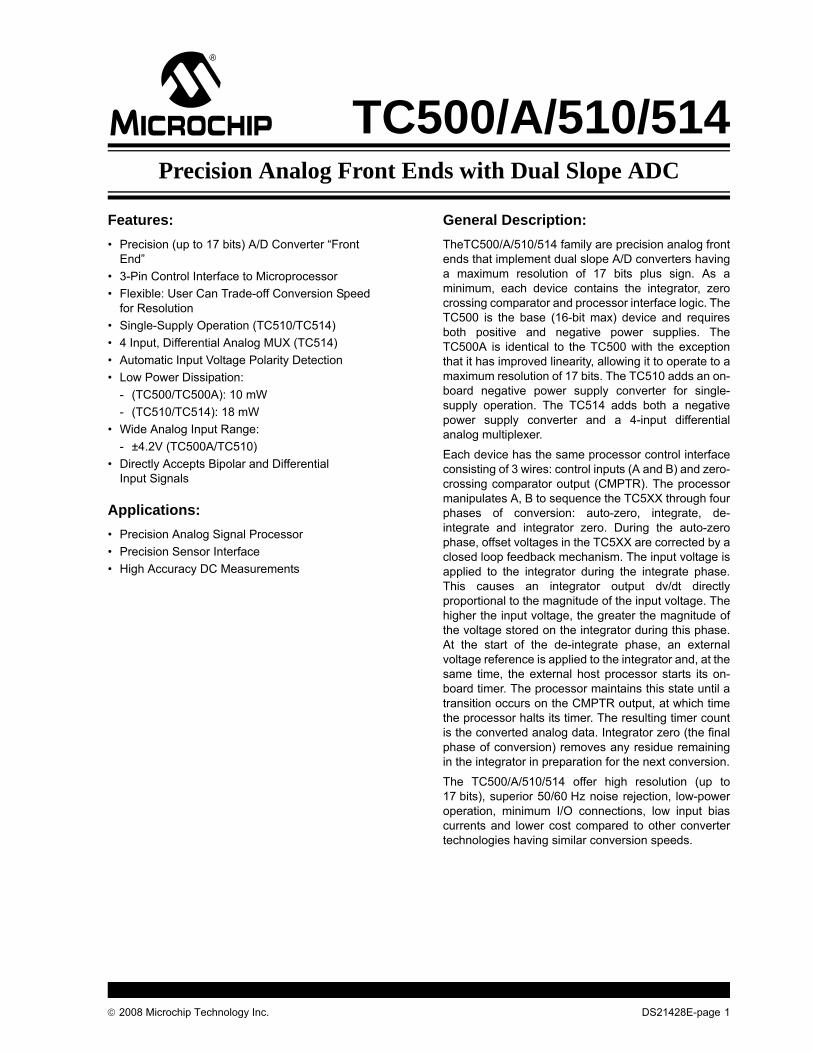
Package TypesTypical Application
1
2
3
4
16
15
14
13
5
6
7
12
11
10
98
CMPTR OUT
A
DGND
B
VDD
VIN+
VIN–
VREF+
BUF
VSS
CINT
ACOM
VREF−
CREF+
CREF–
CAZ
TC500/TC500A
16-Pin PDIP/SOIC/CERDIP
VOUT– 1
2
3
4
20
19
18
CAP–
5
6
7
8
17
23
22
21
9
10
11
12
24
25
26
27
28
DGND
A
B
CREF –
CINT
CAZ
BUF
ACOM
CH4–
CH3–
CH2–
TC514CREF+
VREF –
VREF+
VDD
OSC
CMPTR OUT
CAP+
16
15
13
14
CH1–
N/C
CH1+
CH2+
CH3+
CH4+
A0
A1
28-Pin PDIP/SOIC
24-Pin PDIP/SOIC
1
2
3
4
16
15
14
5
6
7
8
13
19
18
17
9
10
11
12
20
21
22
23
24
TC510
CAP–
DGND
A
B
VDD
OSC
CMPTR OUT
VIN+
VIN–
N/C
N/C
CAP+
CREF–
CINT
CAZ
BUF
ACOM
N/C
N/C
N/C
VOUT–
CREF+
VREF–
VREF+
LevelShift
Control Logic
AnalogSwitchControlSignals
ACOM
VREF+BUF
CAZ
Buffer IntegratorSWR
SWIZ
CMPTR 1CMPTR 2
CMPTROutput
DGND
Control Logic
SW1
TC500TC500ATC510TC514
CREF
CREF+
SWR
CREF- CAZ
RINT CINT
CINT
SWRI- SWRI-
SWRI+ SWRI-SWZ
SWI
SWZ
VSS
OSC
+
+
+
PhaseDecoding
Logic
PolarityDetection
DC-TO-DCConverter
(TC510 & TC514)
-
+
A B 0 0 Zero Integrator Output 0 1 Auto-Zero 1 0 Signal Integrate 1 1 De-integrateVREF-
VOUT-
COUT-1.0 μF
1.0 μFVSS
SWI
BA
A0 A1
DIF.MUX
(TC514)
CH1+CH2+CH3+CH4+CH1-CH2-CH3-CH4-
CAP- CAP+
(TC500TC500A)
Converter Sate
DS21428E-page 2 © 2008 Microchip Technology Inc.

TC500/A/510/514
1.0 ELECTRICAL CHARACTERISTICS
Absolute Maximum Ratings†TC510/TC514 Positive Supply Voltage
(VDD to GND) .........................................+10.5VTC500/TC500A Supply Voltage
(VDD to VSS) ..............................................+18VTC500/TC500A Positive Supply Voltage
(VDD to GND) ............................................+12VTC500/TC500A Negative Supply Voltage
(VSS to GND)................................................-8VAnalog Input Voltage (VIN+ or VIN-) ............VDD to VSSLogic Input Voltage...............VDD +0.3V to GND - 0.3VVoltage on OSC:........................... -0.3V to (VDD +0.3V) for VDD < 5.5VAmbient Operating Temperature Range:................................................................ 0°C to +70°CStorage Temperature Range:............. -65°C to +150°C
† Notice: Stresses above those listed under “AbsoluteMaximum Ratings” may cause permanent damage tothe device. These are stress ratings only and functionaloperation of the device at these or any other conditionsabove those indicated in the operation sections of thespecifications is not implied. Exposure to AbsoluteMaximum Rating conditions for extended periods mayaffect device reliability.
DC CHARACTERISTICSElectrical Specifications: Unless otherwise specified, TC510/TC514: VDD = +5V, TC500/TC500A: VSS
= ±5V. CAZ = CREF = 0.47 μF.
Parameters SymTA = +25°C TA = 0°C to 70°C
Units ConditionsMin. Typ. Max. Min. Typ. Max.
AnalogResolution 60 — — — — — μV Note 1Zero-scale Error with Auto-zero Phase
ZSE — — 0.005 — 0.005 0.012 % F.S. TC500/TC510/TC514— — 0.003 — 0.003 0.009 TC500A
End Point Linearity ENL — 0.005 0.015 — 0.015 0.060 % F.S. TC500/TC510/TC514— — 0.010 — 0.010 0.045 % F.S. Note 1, Note 2,
TC500ABest-Case Straight Line Linearity
NL — 0.003 0.008 — — — % F.S. TC500/TC510/TC514, Note 1, Note 2
— — 0.005 — — — % F.S. TC500AZero-scale Temp. Coefficient
ZSTC — — — — 1 2 μV/°C Over Operating Temperature Range
Full-scale Symmetry Error (Rollover Error)
SYE — 0.01 — — 0.03 — % F.S. Note 1
Full-scale Temperature Coefficient
FSTC — — — — 10 — ppm/°C Over Operating Temperature Range; External Reference TC = 0 ppm/°C
Input Current IIN — 6 — — — — pA VIN = 0V Common Mode Voltage Range
VCMR VSS + 1.5 — VDD – 1.5 VSS + 1.5 — VDD – 1.5 V
Integrator Output Swing
VSS + 0.9 — VDD – 0.9 VSS + 0.9 — VSS + 0.9 V
Analog Input Signal Range
VSS + 1.5 — VDD – 1.5 VSS + 1.5 — VSS + 1.5 V ACOM = GND = 0V
Note 1: Integrate time ≥ 66 ms, auto-zero time ≥ 66 ms, VINT (peak) ≈ 4V.2: End point linearity at ±1/4, ±1/2, ±3/4 F.S. after full-scale adjustment.3: Rollover error is related to CINT, CREF, CAZ characteristics.
© 2008 Microchip Technology Inc. DS21428E-page 3

TC500/A/510/514
Voltage Reference Range
VREF VSS +1 — VDD – 1 VSS +1 — VDD – 1 V VREF- VREF+
DigitalComparator Logic 1, Output High
VOH 4 — — 4 — — V ISOURCE = 400 μA
Comparator Logic 0, Output Low
VOL — — 0.4 — — 0.4 V ISINK = 2.1 mA
Logic 1, Input High Voltage
VIH 3.5 — — 3.5 — — V
Logic 0, Input Low Voltage
VIL — — 1 — — 1 V
Logic Input Current IL — — — — 0.3 μA Logic ‘1’ or ‘0’Comparator Delay tD — 2 — — 3 — μsMultiplexer (TC514 Only)Maximum Input Voltage
-2.5 — 2.5 -2.5 — 2.5 V VDD = 5V
Drain/Source ON Resistance
RDSON — 6 10 — — — kΩ VDD = 5V
Power (TC510/TC514 Only)Supply Current IS — 1.8 2.4 — — 3.5 mA VDD = 5V, A = 1, B = 1Power Dissipation PD — 18 — — — — mW VDD = 5VPositive Supply Operating Voltage Range
VDD 4.5 — 5.5 4.5 — 5.5 V
Operating Source Resistance
ROUT — 60 85 — — 100 Ω IOUT = 10 mA
Oscillator Frequency — 100 — — — — kHz Note 1Maximum Current Out
IOUT — — -10 — — -10 mA VDD = 5V
Power (TC500/TC500A Only)Supply Current IS — 1 1.5 — — 2.5 mA VS = ±5V, A = B = 1Power Dissipation PD — 10 — — — — mW VDD = 5V, VSS = -5VPositive Supply Operating Range
VDD 4.5 — 7.5 4.5 — 7.5 V
Negative Supply Operating Range
VSS -4.5 — -7.5 - 4.5 — -7.5 V
DC CHARACTERISTICS (CONTINUED)Electrical Specifications: Unless otherwise specified, TC510/TC514: VDD = +5V, TC500/TC500A: VSS
= ±5V. CAZ = CREF = 0.47 μF.
Parameters SymTA = +25°C TA = 0°C to 70°C
Units ConditionsMin. Typ. Max. Min. Typ. Max.
Note 1: Integrate time ≥ 66 ms, auto-zero time ≥ 66 ms, VINT (peak) ≈ 4V.2: End point linearity at ±1/4, ±1/2, ±3/4 F.S. after full-scale adjustment.3: Rollover error is related to CINT, CREF, CAZ characteristics.
DS21428E-page 4 © 2008 Microchip Technology Inc.
TC500/A/510/514
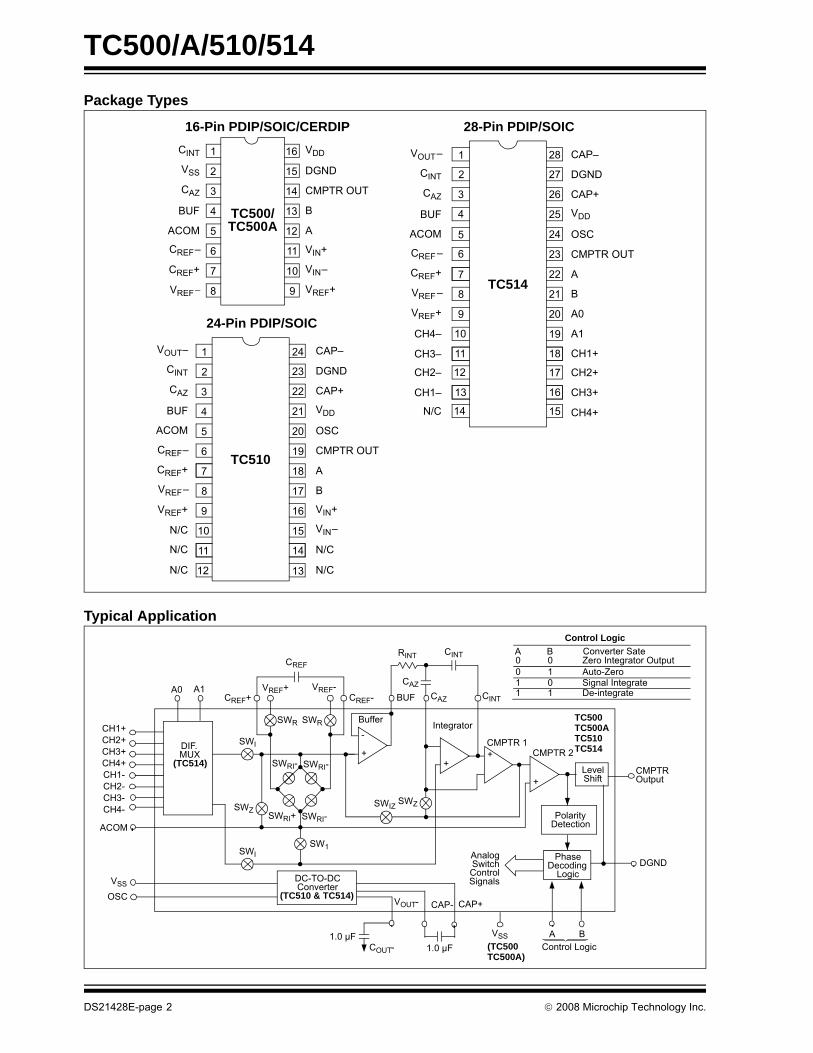
2.0 TYPICAL PERFORMANCE CURVES
FIGURE 2-1: Output Voltage vs. Load Current.
FIGURE 2-2: Output Ripple vs. Load Current.
FIGURE 2-3: Oscillator Frequency vs. Capacitance.
FIGURE 2-4: Output Voltage vs. Output Current.
FIGURE 2-5: Output Source Resistance vs. Temperature.
FIGURE 2-6: Oscillator Frequency vs. Temperature.
Note: The graphs and tables provided following this note are a statistical summary based on a limited number ofsamples and are provided for informational purposes only. The performance characteristics listed hereinare not tested or guaranteed. In some graphs or tables, the data presented may be outside the specifiedoperating range (e.g., outside specified power supply range) and therefore outside the warranted range.
Load Current (mA)
-5
-4
-3
-2
-1
0
1
2
3
4
5
0 10 20 30 40 50 60 70 80
Outp
ut V
oltage (
V)
TA = +25°C
V+ = 5V
Slope 60Ω
Load Current (mA)
0 3 4 5 61 2 7 8 9 100
25
50
75
100
125
150
175
200
Ou
tpu
t R
ipp
le (
mV
PK
-PK
) V+ = 5V, TA = +25°COsc. Freq. = 100 kHz
CAP = 1 µF
CAP = 10 µF
Oscillator Capacitance (pF)
100
10
11 10 100 1000
Oscill
ato
r F
req
ue
ncy (
kH
z) TA = +25°C
V+ = 5V
Output Current (mA)
0 6 8 1042 14 16 1812 20
-0
-1
-3
-2
-4
-5
-7
-6
-8
Ou
tpu
t V
olta
ge
(V
)
TA = +25°C
Temperature (°C)
70
80
90
100
60
50
40-50 0 25-25 50 75 100
Ou
tpu
t S
ou
rce
Re
sis
tan
ce
(Ω
) V+ = 5VIOUT = 10 mA
Temperature (°C)
125
150
100
75
50-50 0 25-25 50 75 125100
Oscill
ato
r F
req
ue
ncy (
kH
z)
V+ = 5V
© 2008 Microchip Technology Inc. DS21428E-page 5

TC500/A/510/514
NOTES:DS21428E-page 6 © 2008 Microchip Technology Inc.
TC500/A/510/514
3.0 PIN DESCRIPTIONSThe descriptions of the pins are listed in Table 3-1.
TABLE 3-1: PIN FUNCTION TABLETC500, TC500A TC510 TC514 Symbol Function
CERDIP, PDIP, SOIC PDIP, SOIC PDIP, SOIC
1 2 2 CINT Integrator output. Integrator capacitor connection.2 Not Used Not Used VSS Negative power supply input (TC500/TC500A only).3 3 3 CAZ Auto-zero input. The auto-zero capacitor connection.4 4 4 BUF Buffer output. The Integrator capacitor connection.5 5 5 ACOM This pin is grounded in most applications. It is recommended that
ACOM and the input common pin (Ven- or CHn-) be within the analog Common Mode Range (CMR).
6 6 6 CREF- Input. Negative reference capacitor connection.7 7 7 CREF+ Input. Positive reference capacitor connection.8 8 8 VREF- Input. External voltage reference (-) connection.9 9 9 VREF+ Input. External voltage reference (+) connection.
10 15 Not Used VIN- Negative analog input.11 16 Not Used VIN+ Positive analog input.12 18 22 A Input. Converter phase control MSB. (See input B.)13 17 21 B Input. Converter phase control LSB. The states of A, B place the
TC5XX in one of four required phases. A conversion is complete when all four phases have been executed:Phase control input pins: AB = 00: Integrator zero
01: Auto-zero10: Integrate11: De-integrate
14 19 23 CMPTR OUT Zero crossing comparator output. CMPTR is high during the integration phase when a positive input voltage is being integrated and is low when a negative input voltage is being integrated. A high-to-low transition on CMPTR signals the processor that the De-integrate phase is completed. CMPTR is undefined during the auto-zero phase. It should be monitored to time the integrator zero phase.
15 23 27 DGND Input. Digital ground.16 21 25 VDD Input. Power supply positive connection.— 22 26 CAP+ Input. Negative power supply converter capacitor (+) connection.— 24 28 CAP- Input. Negative power supply converter capacitor (-) connection.— 1 1 VOUT- Output. Negative power supply converter output and reservoir
capacitor connection. This output can be used to power other devices in the circuit requiring a negative bias voltage.
— 20 24 OSC Oscillator control input. The negative power supply converter normally runs at a frequency of 100 kHz. The converter oscillator frequency can be slowed down (to reduce quiescent current) by connecting an external capacitor between this pin and VDD (see Section 2.0 “Typical Performance Curves”).
— — 18 CH1+ Positive analog input pin. MUX channel 1.— — 13 CH1- Negative analog input pin. MUX channel 1.— — 17 CH2+ Positive analog input pin. MUX channel 2.— — 12 CH2- Negative analog input pin. MUX channel 2.— — 16 CH3+ Positive analog input pin. MUX channel 3.— — 11 CH3- Negative analog input pin. MUX channel 3.— — 15 CH4+ Positive analog input pin. MUX channel 4.— — 10 CH4- Negative analog input pin. MUX channel 4— — 20 A0 Multiplexer input channel select input LSB (see A1).
© 2008 Microchip Technology Inc. DS21428E-page 7
TC500/A/510/514
— — 19 A1 Multiplexer input channel select input MSB.Phase control input pins: A1, A0 = 00 = Channel 1
01 = Channel 210 = Channel 311 = Channel 4
TABLE 3-1: PIN FUNCTION TABLE (CONTINUED)TC500, TC500A TC510 TC514 Symbol Function
CERDIP, PDIP, SOIC PDIP, SOIC PDIP, SOIC
DS21428E-page 8 © 2008 Microchip Technology Inc.
TC500/A/510/514
4.0 DETAILED DESCRIPTION
4.1 Dual Slope Conversion Principles Actual data conversion is accomplished in twophases: input signal integration and reference voltagede-integration.
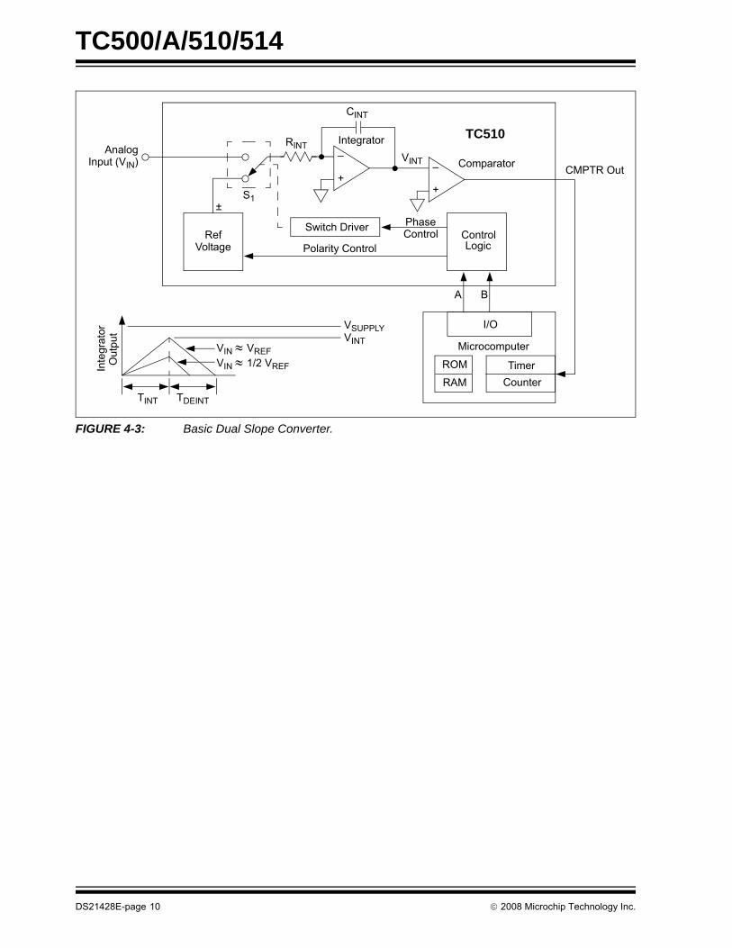
The integrator output is initialized to 0V prior to the startof integration. During integration, analog switch S1connects VIN to the integrator input where it ismaintained for a fixed time period (TINT). Theapplication of VIN causes the integrator output to depart0V at a rate determined by the magnitude of VIN and adirection determined by the polarity of VIN. The de-integration phase is initiated immediately at theexpiration of TINT.
During de-integration, S1 connects a reference voltage(having a polarity opposite that of VIN) to the integratorinput. At the same time, an external precision timer isstarted. The de-integration phase is maintained untilthe comparator output changes state, indicating theintegrator has returned to its starting point of 0V. Whenthis occurs, the precision timer is stopped. The de-integration time period (TDEINT), as measured by theprecision timer, is directly proportional to the magnitudeof the applied input voltage (see Figure 4-3).
A simple mathematical equation relates the inputsignal, reference voltage and integration time:
EQUATION 4-1:
For a constant VIN:
EQUATION 4-2:
The dual slope converter accuracy is unrelated to theintegrating resistor and capacitor values as long asthey are stable during a measurement cycle.
An inherent benefit is noise immunity. Input noisespikes are integrated (averaged to zero) during theintegration periods. Integrating ADCs are immune tothe large conversion errors that plague successiveapproximation converters in high noise environments.
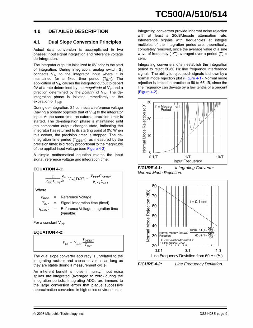
Integrating converters provide inherent noise rejectionwith at least a 20dB/decade attenuation rate.Interference signals with frequencies at integralmultiples of the integration period are, theoretically,completely removed, since the average value of a sinewave of frequency (1/T) averaged over a period (T) iszero.
Integrating converters often establish the integrationperiod to reject 50/60 Hz line frequency interferencesignals. The ability to reject such signals is shown by anormal mode rejection plot (Figure 4-1). Normal moderejection is limited in practice to 50 to 65 dB, since theline frequency can deviate by a few tenths of a percent(Figure 4-2).
FIGURE 4-1: Integrating Converter Normal Mode Rejection.
FIGURE 4-2: Line Frequency Deviation.
Where:
VREF = Reference VoltageTINT = Signal Integration time (fixed)
tDEINT = Reference Voltage Integration time (variable)
1RINTCINT------------------------ VIN T( )DT
0TINT∫
VREFCDEINTRINTCINT
--------------------------------=
VIN VREFTDEINT
TINT------------------=
30
20
10
0
0.1/T 1/T 10/TInput Frequency
Norm
al M
ode R
eje
ction (
dB
)
T = Measurment Period
0.01 0.1 1.0
Nor
mal
Mod
e R
ejec
iton
(dB
)
80
70
60
50
40
30
20
t = 0.1 sec
Line Frequency Deviation from 60 Hz (%)
Normal Mode = 20 LOGRejectionDEV = Deviation from 60 Hzt = Integration Period
SIN 60 t (1 – )p
p
DEV100DEV10060 t (1 – )
© 2008 Microchip Technology Inc. DS21428E-page 9
TC500/A/510/514
FIGURE 4-3: Basic Dual Slope Converter.
PhaseControl
Comparator
Inte
grat
orO
utpu
t
Integrator
CINT
AnalogInput (VIN)
Switch DriverRef
VoltageControlLogicPolarity Control
S1
I/O
TimerCounter
ROM
RAM
Microcomputer
A B
CMPTR Out
VSUPPLY
±
TINT
TC510
VINTVIN ≈ VREFVIN ≈ 1/2 VREF
TDEINT
–
+
RINTVINT–
+
DS21428E-page 10 © 2008 Microchip Technology Inc.

TC500/A/510/514
5.0 TC500/A/510/514 CONVERTER OPERATION
The TC500/A/510/514 incorporates an auto-zero andIntegrator phase in addition to the input signal Integrateand reference De-integrate phases. The addition ofthese phases reduce system errors, calibration stepsand shorten overrange recovery time. A typicalmeasurement cycle uses all four phases in thefollowing order:
1. Auto-zero.2. Input signal integration.3. Reference de-integration.4. Integrator output zero.
The internal analog switch status for each of thesephases is summarized in Table 5-1. This tablereferences the Typical Application.
TABLE 5-1: INTERNAL ANALOG GATE STATUS
5.1 Auto-zero Phase (AZ)During this phase, errors due to buffer, integrator andcomparator offset voltages are nulled out by chargingCAZ (auto-zero capacitor) with a compensating errorvoltage.
The external input signal is disconnected from theinternal circuitry by opening the two SWI switches. Theinternal input points connect to analog common. Thereference capacitor is charged to the reference voltagepotential through SWR. A feedback loop, closed aroundthe integrator and comparator, charges the capacitor(CAZ) with a voltage to compensate for buffer amplifier,integrator and comparator offset voltages.
5.2 Analog Input Signal Integration Phase (INT)
The TC5XX integrates the differential voltage betweenthe VIN+ and VIN– inputs. The differential voltage mustbe within the device’s Common mode range VCMR. Theinput signal polarity is normally checked via software atthe end of this phase: CMPTR = 1 for positive polarity;CMPTR = 0 for negative polarity.
5.3 Reference Voltage De-integration Phase (DINT)
The previously charged reference capacitor isconnected with the proper polarity to ramp theintegrator output back to zero. An externally-provided,precision timer is used to measure the duration of thisphase. The resulting time measurement is proportionalto the magnitude of the applied input voltage.
5.4 Integrator Output Zero Phase (IZ)This phase ensures the integrator output is at 0V whenthe auto-zero phase is entered, and that only systemoffset voltages are compensated. This phase is used atthe end of the reference voltage de-integration phaseand MUST be used for ALL TC5XX applications havingresolutions of 12-bits or more. If this phase is not used,the value of the auto-zero capacitor (CAZ) must beabout 2 to 3 times the value of the integration capacitor(CINT) to reduce the effects of charge sharing. Theintegrator output zero phase should be programmed tooperate until the output of the comparator returns high.The overall timing system is shown in Figure 5-1.
Conversion Phase SWI SWR+ SWR- SWZ SWR SW1 SWIZ
Auto-zero (A = 0, B = 1) — — — Closed Closed Closed —Input Signal Integration (A = 1, B = 0) Closed — — — — — —Reference Voltage De-integration (A =1, B = 1) —
*Closed — — — Closed —
Integrator Output Zero (A = 0, B = 0) — — — — Closed Closed Closed
* Assumes a positive polarity input signal. SW–RI would be closed for a negative input signal.
© 2008 Microchip Technology Inc. DS21428E-page 11

TC500/A/510/514
FIGURE 5-1: Typical Dual Slope A/D Converter System Timing.
Auto-zero IntegrateFull-scale Input
ReferenceDe-integrate
Overshoot IntegratorOutputZero
Converter Status
TTIME
IntegratorVoltage VINT
ComparatorOutput
AB Inputs
ControllerOperation
Notes:
Comparator Delay
Begin Conversion withAuto-Zero Phase
(Positive Input Shown)
Sample Input Polarity
The length of this phase is chosen almost arbitrarilybut needs to be long enough to null out worst case errors(see text).
MinimizingOvershootwill MinimizeI.O.Z. Time
Ready for NextConversion(Auto-Zero is Idle State)
Time Input IntegrationPhase
CaptureDe-integrationTime
IntegratorOutputZero PhaseComplete
Undefined
A = 0
B = 1
A = 1
0 For Negative Input1 For Positive Input
B = 0 B = 1 B = 0
A = 1 A = 0
Typically = TINT TINT
0
A
B
Comparator Delay +Processor Latency
DS21428E-page 12 © 2008 Microchip Technology Inc.

TC500/A/510/514
6.0 ANALOG SECTION
6.1 Differential Inputs (VIN+, VIN–)The TC5XX operates with differential voltages withinthe input amplifier Common mode range. The amplifierCommon mode range extends from 1.5V belowpositive supply to 1.5V above negative supply. Withinthis Common mode voltage range, Common moderejection is typically 80 dB. Full accuracy is maintained,however, when the inputs are no less than 1.5V fromeither supply.
The integrator output also follows the Common modevoltage. The integrator output must not be allowed tosaturate. A worst-case condition exists, for example,when a large, positive Common mode voltage, with anear full-scale negative differential input voltage, isapplied. The negative input signal drives the integratorpositive when most of its swing has been used up bythe positive Common mode voltage. For these criticalapplications, the integrator swing can be reduced. Theintegrator output can swing within 0.9V of either supplywithout loss of linearity.
6.2 Analog CommonAnalog common is used as VIN return during systemzero and reference de-integrate. If VIN– is different fromanalog common, a Common mode voltage exists in thesystem. This signal is rejected by the excellent CMR ofthe converter. In most applications, VIN– will be set at afixed known voltage (i.e., power supply common). ACommon mode voltage will exist when VIN– is notconnected to analog common.
6.3 Differential Reference (VREF+, VREF–)
The reference voltage can be anywhere within 1V ofthe power supply voltage of the converter. Rollovererror is caused by the reference capacitor losing orgaining charge due to stray capacitance on its nodes.
The difference in reference for (+) or (-) input voltageswill cause a rollover error. This error can be minimizedby using a large reference capacitor in comparison tothe stray capacitance.
6.4 Phase Control Inputs (A, B) The A, B unlatched logic inputs select the TC5XXoperating phase. The A, B inputs are normally drivenby a microprocessor I/O port or external logic.
6.5 Comparator OutputBy monitoring the comparator output during the fixedsignal integrate time, the input signal polarity can bedetermined by the microprocessor controlling theconversion. The comparator output is high for positivesignals and low for negative signals during the signalintegrate phase (see Figure 6-1).
During the reference de-integrate phase, thecomparator output will make a high-to-low transition asthe integrator output ramp crosses zero. The transitionis used to signal the processor that the conversion iscomplete.
The internal comparator delay is 2 μs, typically.Figure 6-1 shows the comparator output for largepositive and negative signal inputs. For signal inputs ator near zero volts, however, the integrator swing is verysmall. If Common mode noise is present, thecomparator can switch several times during thebeginning of the signal integrate period. To ensure thatthe polarity reading is correct, the comparator outputshould be read and stored at the end of the signalintegrate phase.
The comparator output is undefined during the auto-zero phase and is used to time the integrator outputzero phase. (See Section 8.6 “Integrator Output ZeroPhase”).
FIGURE 6-1: Comparator Output.
IntegratorOutput
ZeroCrossing
ComparatorOutput
ReferenceSignalIntegrate
IntegratorOutput
ZeroCrossing
ComparatorOutput
ReferenceDeintegrate
SignalIntegrate
B. Negative Input SignalA. Positive Input Signal
De-integrate
© 2008 Microchip Technology Inc. DS21428E-page 13

TC500/A/510/514
NOTES:DS21428E-page 14 © 2008 Microchip Technology Inc.
TC500/A/510/514
7.0 TYPICAL APPLICATIONS
7.1 Component Value SelectionThe procedure outlined below allows the user to arriveat values for the following TC5XX design variables:
1. Integration Phase Timing.2. Integrator Timing Components (RINT, CINT).3. Auto-zero and Reference Capacitors.4. Voltage Reference.
7.2 Select Integration TimeIntegration time must be picked as a multiple of theperiod of the line frequency. For example, TINT times of33 ms, 66 ms and 132 ms maximize 60 Hz linerejection.
7.3 DINT and IZ Phase TimingThe duration of the DINT phase is a function of theamount of voltage stored on the integrator during TINTand the value of VREF. The DINT phase must be initiatedimmediately following INT and terminated when anintegrator output zero-crossing is detected. In general,the maximum number of counts chosen for DINT is twicethat of INT (with VREF chosen at VIN(MAX) /2).
7.4 Calculate Integrating Resistor (RINT)
The desired full-scale input voltage and amplifier outputcurrent capability determine the value of RINT. Thebuffer and integrator amplifiers each have a full-scalecurrent of 20 μA.
The value of RINT is, therefore, directly calculated in thefollowing equation:
EQUATION 7-1:
7.5 Select Reference (CREF) and Auto-zero (CAZ) Capacitors
CREF and CAZ must be low leakage capacitors (such aspolypropylene). The slower the conversion rate, thelarger the value CREF must be. Recommendedcapacitors for CREF and CAZ are shown in Table 7-1.Larger values for CAZ and CREF may also be used tolimit rollover errors.
TABLE 7-1: CREF AND CAZ SELECTION
7.6 Calculate Integrating Capacitor (CINT)
The integrating capacitor must be selected to maximizeintegrator output voltage swing. The integrator outputvoltage swing is defined as the absolute value of VDD(or VSS) less 0.9V (i.e., IVDD - 0.9VI or IVSS + 0.9VI).Using the 20 μA buffer maximum output current, thevalue of the integrating capacitor is calculated using thefollowing equation.
EQUATION 7-2:
It is critical that the integrating capacitor has a very lowdielectric absorption. Polypropylene capacitors are anexample of one such dialectic. Polyester and poly-bicarbonate capacitors may also be used in less criticalapplications. Table 7-2 summarizes recommendedcapacitors for CINT.
TABLE 7-2: RECOMMENDED CAPACITOR FOR CINT
7.7 Calculate VREFThe reference de-integration voltage is calculatedusing the following equation:
EQUATION 7-3:
Where:
VIN(MAX) = Maximum input voltage (full count voltage)
RINT = Integrating Resistor (in MΩ)
For loop stability, RINT should be ≥ 50 kΩ
RINT in MΩ( )VIN MAX( )
20-----------------------=
ConversionsPer Second
Typical Value of CREF, CAZ (μF)
Suggested* Part Number
>7 0.1 SMR5 104K50J01L42 to 7 0.22 SMR5 224K50J02L4
2 or less 0.47 SMR5 474K50J04L4
* Manufactured by Evox Rifa, Inc.
Value Suggested Part Number*
0.1 SMR5 104K50J01L40.22 SMR5 224K50J02L40.33 SMR5 334K50J03L40.47 SMR5 474K50J04L4
* Manufactured by Evox Rifa, Inc.
Where:
TINT = Integration PeriodVS = IVDDI or IVSSI, whichever is less
(TC500/A)VS = IVDDI (TC510, TC514)
CINTTINT( ) 20 10 6–×( )
VS 0.9–( )---------------------------------------------=
VREFVS 0.9–( ) CINT( ) RINT( )
2 TINT( )-----------------------------------------------------------V=
© 2008 Microchip Technology Inc. DS21428E-page 15

TC500/A/510/514
NOTES:DS21428E-page 16 © 2008 Microchip Technology Inc.
TC500/A/510/514
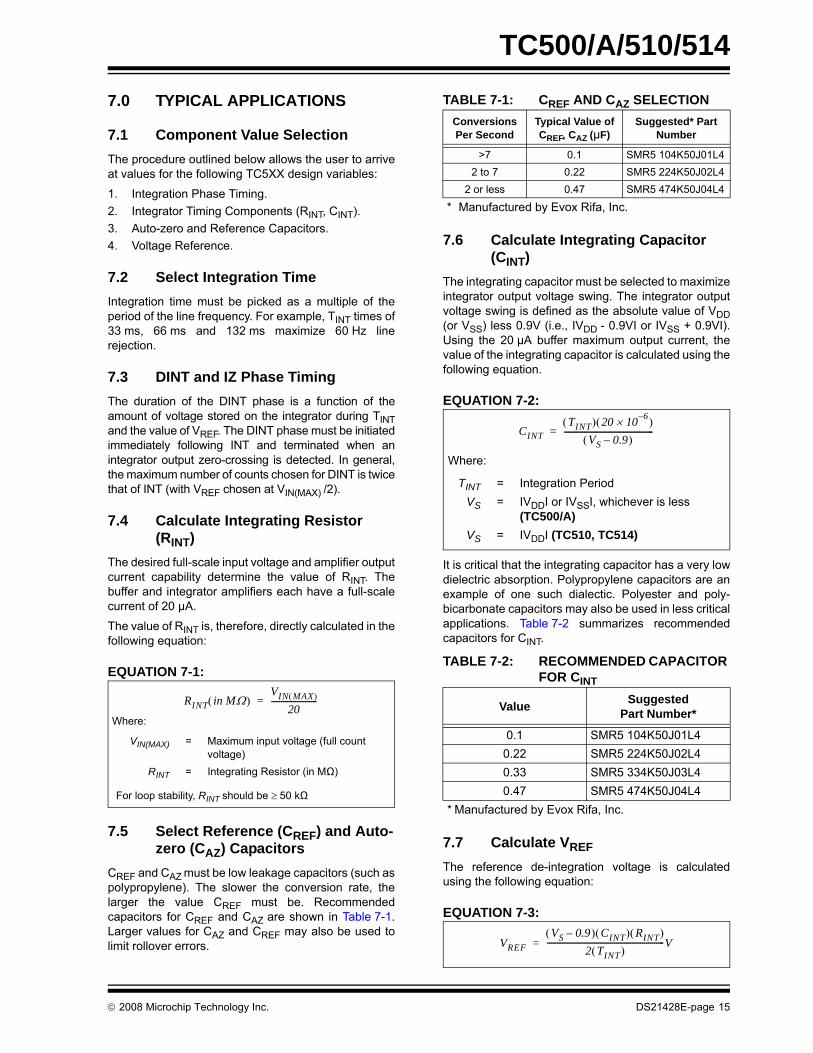
8.0 DESIGN CONSIDERATIONS
8.1 NoiseThe threshold noise (NTH) is the algebraic sum of theintegrator and comparator noise and is typically 30 μV.Figure 8-1 illustrates how the value of the referencevoltage can affect the final count. Such errors can bereduced by increased integration times, in the sameway that 50/60 Hz noise is rejected. The signal-to-noise ratio is related to the integration time (TINT) andthe integration time constant (RINT, CINT) as follows:
EQUATION 8-1:
8.2 System TimingTo obtain maximum performance from the TC5XX, theovershoot at the end of the de-integration phase mustbe minimized. Also, the integrator output zero phasemust be terminated as soon as the comparator outputreturns high (see Figure 5-1).
Figure 5-1 shows the overall timing for a typical systemin which a TC5XX is interfaced to a microcontroller. Themicrocontroller drives the A, B inputs with I/O lines andmonitors the comparator output (CMPTR) using an I/Oline or dedicated timer capture control pin. It may benecessary to monitor the state of the CMPTR output inaddition to having it control a timer directly for theReference de-integration phase (this is furtherexplained below.)
The timing diagram in Figure 5-1 is not to scale, as thetiming in a real system depends on many systemparameters and component value selections. Thereare four critical timing events (as shown in Figure 5-1):sampling the input polarity, capturing the de-integrationtime, minimizing overshoot and properly executing theintegrator output zero phase.
8.3 Auto-zero PhaseThe length of this phase is usually set to be equal to theinput signal integration time. This decision is virtuallyarbitrary since the magnitudes of the various systemerrors are not known. Setting the auto-zero time equalto the Input Integrate time should be more thanadequate to null out system errors. The system mayremain in this phase indefinitely (i.e., auto-zero is theappropriate Idle state for a TC5XX device).
8.4 Input Signal Integrate PhaseThe length of this phase is constant from oneconversion to the next and depends on systemparameters and component value selections. Thecalculation of TINT is shown elsewhere in this datasheet. At some point near the end of this phase, themicrocontroller should sample CMPTR to determinethe input signal polarity. This value is, in effect, the SignBit for the overall conversion result. Optimally, CMPTRshould be sampled just before this phase is terminatedby changing AB from 10 to 11. The consideration hereis that, during the initial stage of input integration whenthe integrator voltage is low, the comparator may beaffected by noise and its output unreliable. Onceintegration is well underway, the comparator will be in adefined state.
8.5 Reference De-integrationThe length of this phase must be precisely measuredfrom the transition of AB from 10 to 11 to the falling-edge of CMPTR. The comparator delay contributessome error in timing this phase. The typical delay isspecified to be 2 μs. This should be considered in thecontext of the length of a single count whendetermining overall system performance and possiblesingle count errors. Additionally, overshoot will result incharge accumulating on the integrator once its outputcrosses zero. This charge must be nulled during theintegrator output zero phase.
FIGURE 8-1: Noise Threshold.
S/N (dB) 20 logVIN
30 10 6–×-----------------------
tINTRINT( ) CINT( )•
---------------------------------------•⎝ ⎠⎜ ⎟⎛ ⎞
=
Low VREF Normal VREF High VREF
S
NTH
S
NTH
30 µV
S
NTH
Slope (S) = NTH = Noise ThresholdVREF
RINT CINT
© 2008 Microchip Technology Inc. DS21428E-page 17
TC500/A/510/514
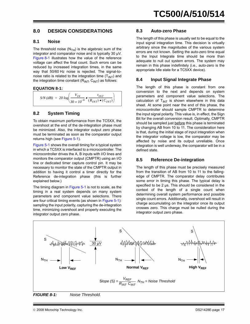
8.6 Integrator Output Zero PhaseThe comparator delay and the controller’s responselatency may result in overshoot, causing chargebuildup on the integrator at the end of a conversion.This charge must be removed or performance willdegrade. The integrator output zero phase should beactivated (AB = 00) until CMPTR goes high. It isabsolutely critical that this phase be terminatedimmediately so that overshoot is not allowed to occur inthe opposite direction. At this point, it can be assuredthat the integrator is near zero. Auto-zero should beentered (AB = 01) and the TC5XX held in this state untilthe next cycle is begun (see Figure 8-2).FIGURE 8-2: Overshoot.
8.7 Using the TC510/TC514
8.7.1 NEGATIVE SUPPLY VOLTAGE CONVERTER (TC510, TC514)
A capacitive charge pump is employed to invert thevoltage on VDD for negative bias within the TC510/TC514. This voltage is also available on the VOUT– pinto provide negative bias elsewhere in the system. Twoexternal capacitors are required to perform theconversion.
Timing is generated by an internal state machine drivenfrom an on-board oscillator. During the first phase,capacitor CF is switched across the power supply andcharged to VS+. This charge is transferred to capacitorCOUT– during the second phase. The oscillatornormally runs at 100 kHz to ensure minimum outputripple. This frequency can be reduced by placing acapacitor from OSC to VDD. The relationship betweenthe capacitor value is shown in Section 2.0 “TypicalPerformance Curves”.
8.7.2 ANALOG INPUT MULTIPLEXER (TC514)
The TC514 is equipped with a four-input differentialanalog multiplexer. Input channels are selected usingselect inputs (A1, A0). These are high-true controlsignals (i.e., channel 0 is selected when (A1, A0 = 00).
IntegratorOutput
ComparatorOutput Comp
IntegratePhase
De-integrate PhaseIntegrator
Zero Phase
ZeroCrossing
Overshoot
DS21428E-page 18 © 2008 Microchip Technology Inc.
TC500/A/510/514
9.0 DESIGN EXAMPLESRefer to Figures 9-1 to 9-4.
EQUATION 9-1:
Given: Required Resolution: 16 bits (65,536 counts).Maximum VIN: ±2VPower Supply Voltage: +5V60 Hz System
Step 1. Pick integration time (tINT) as a multiple of the line frequency:1/60 Hz = 16.6 ms. Use 4x line frequency.= 66 ms
Step 2. Calculate RINT:RINT = VIN(MAX) /20 μA 2 /20 μA= 100 kΩ
Step 3. Calculate CINT for maximum (4V) integrator output swing.CINT = (tINT) (20 x 10 –6) / (VS - 0.9)= (.066) (20 x 10 –6) / (4.1)= 0.32 μF (use closest value: 0.33 μF)
Note: Microchip recommended capacitor:Evox Rifa p/n: 5MR5 334K50J03L4.
Step 4. Choose CREF and CAZ based on conversion rate.Conversions/sec:= 1/(TAZ + TINT + 2 TINT + 2 ms)= 1/(66 ms +66 ms +132 ms +2 ms)= 3.7 conversions/secFrom which CAZ = CREF = 0.22 μF (see Table 7-1)
Note: Microchip recommended capacitor:Evox Rifa p/n: 5MR5 224K50J02L4
Step 5. Calculate VREF:
VREFVS 0.9–( ) CINT( ) RINT( )
2 TINT( )-----------------------------------------------------------=
4.1( ) 0.33 10 6–×( ) 100 103×( )
2 66 10 3–×( )--------------------------------------------------------------------------=
1.025 V( )=
© 2008 Microchip Technology Inc. DS21428E-page 19
TC500/A/510/514
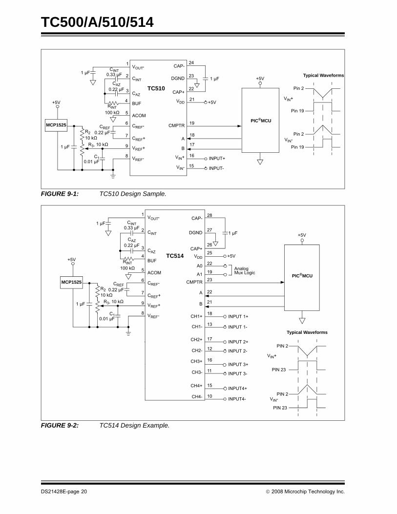
FIGURE 9-1: TC510 Design Sample.
FIGURE 9-2: TC514 Design Example.
INPUT+
INPUT-
+5V
+5V
Pin 2
Pin 19
Pin 2
Pin 19
CINT0.33 μF
VIN+
Typical Waveforms1 μF1 μF
CAZ0.22 μF
CREF
VIN-
RINT100 kΩ
1
2
3
4
16
15
CAP-
5
6
7
9
19
18
17
8
21
22
23
24
DGND
VREF+
VOUT-
A
B
CREF-
CINT
CAZ
BUF
ACOM
TC510
VREF- VIN+
VIN-
CAP+
VDD
CMPTR0.22 μF
C10.01 μF
R210 kΩ
+5V
R3, 10 kΩ
MCP1525
1 μF
CREF+
PIC®MCU
+5V
+5V
PIN 2
PIN 23
PIN 2
PIN 23
VIN+
Typical Waveforms
1 μF
VIN-
CAP-
23
22
21
25
26
27
28
DGND
A
B
TC514CAP+
VDD
CMPTR
AnalogMux Logic
INPUT 1+
INPUT 1-
INPUT 2+
INPUT 2-
INPUT 3+
INPUT 3-
INPUT4+
INPUT4-
18
13
A1
CH1+
17
12
CH2+
CH2-
16
11
CH3+
CH3-
15
10
CH4+
CH4-
22
19 A0
CH1-
CINT0.33 μF
1 μF
CAZ0.22 μF
CREF
RINT100 kΩ
1
2
3
4
5
6
7
9
8
VREF+
VOUT-
CREF-
CINT
CAZ
BUF
ACOM
VREF-
0.22 μF
C10.01 μF
R210 kΩ
+5V
R3, 10 kΩ
MCP1525
1 μF
CREF+
PIC®MCU
DS21428E-page 20 © 2008 Microchip Technology Inc.

TC500/A/510/514
FIGURE 9-3: TC510 To IBM® Compatible Printer Port.
PCPrinter
Port
PORT0378Hex
Input
+
+5V
10 kΩ
10 kΩ
100 kΩ
100 kΩ
1 μF
1 μF121
2
2 3
3
4
16
15
CAP-
5
6
7
8
1910
18
17
9
22
23
24
DGND
VOUT-VDD
A
B CINT
CAZ
BUF
ACOM
TC510
CREF+
VIN+
CAP+
CMPTR
0.22 μF
0.22 μF
0.01 μF
0.01 μF
1 μF
0.33 μF
MCP1525CREF-
VREF+
VREF-
VIN-–
© 2008 Microchip Technology Inc. DS21428E-page 21
TC500/A/510/514
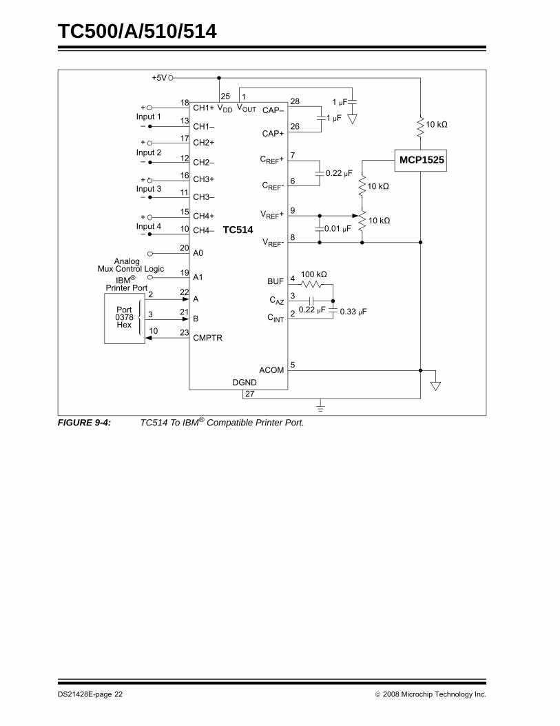
FIGURE 9-4: TC514 To IBM® Compatible Printer Port.
IBM® Printer Port
Port0378Hex
+5V
10 kΩ
100 kΩ
1 μF
1 μF125
2
2 3
3
4
CAP–
5
6
7
8
2310
22
21
9
26
27
28
DGND
VOUTVDD
A
B
CREF+
TC514
BUF
0.22 μF10 kΩ
10 kΩ
0.22 μF
0.01 μF
0.33 μF
CH1+Input 1+ 18
– 13
Input 2+ 17
– 12
Input 3+ 16
– 11
Input 4+ 15
– 10
CAP+
CREF-
VREF+
VREF-
CAZ
CINT
ACOM
CH1–
CH2+
CH2–
CH3+
CH3–
CH4+
CH4–
CMPTR
AnalogMux Control Logic
A0
A1
20
19
MCP1525
DS21428E-page 22 © 2008 Microchip Technology Inc.

TC500/A/510/514
10.0 PACKAGING INFORMATION
10.1 Package Marking Information
16-Lead PDIP (300 mil) (TC500/TC500A) Example:
16-Lead SOIC (300 mil) (TC500/TC500A) Example:
XXXXXXXXXXXXXXXXXXXXXXXXXXXX
YYWWNNN
XXXXXXXXXXX
YYWWNNN
TC500CPE ^^0818256
XXXXXXXXXXX
Legend: XX...X Customer-specific informationY Year code (last digit of calendar year)YY Year code (last 2 digits of calendar year)WW Week code (week of January 1 is week ‘01’)NNN Alphanumeric traceability code Pb-free JEDEC designator for Matte Tin (Sn)* This package is Pb-free. The Pb-free JEDEC designator ( )
can be found on the outer packaging for this package.
Note: In the event the full Microchip part number cannot be marked on one line, it willbe carried over to the next line, thus limiting the number of availablecharacters for customer-specific information.
16-Lead CERDIP (300 mil) (TC500/TC500A) Example:
XXXXXXXXXXXXXXXXXXXXXXXXXXXX
YYWWNNN
TC500AIJE0818256
XXXXXXXXXXX 0818256TC500ACOE ^^
3e
3e
3e
3e
© 2008 Microchip Technology Inc. DS21428E-page 23

TC500/A/510/514
Package Marking Information (Continued)28-Lead PDIP (300 mil) (TC514) Example:
28-Lead SOIC (300 mil) (TC514) Example:
XXXXXXXXXXXXXXXXXXXXXXXXXXXXXXXXXX
YYWWNNN
TC514CPJ ^^0818256
XXXXXXXXXXXXXXXXXXXX
YYWWNNNXXXXXXXXXXXXXXXXXXXX
XXXXXXXXXXXXXXXXXXXX
0818256TC514COI ^^
24-Lead PDIP (300 mil) (TC510) Example:
24-Lead SOIC (300 mil) (TC510) Example:
XXXXXXXXXXXXXXXXXX
YYWWNNNXXXXXXXXXXXXXXXXXX
0818256TC510COG ^^
YYWWNNNXXXXXXXXXXXXXXXXXXXXXXXXXXXXXXXXXX
0818256TC510CPF
3e
3e
3e
DS21428E-page 24 © 2008 Microchip Technology Inc.
TC500/A/510/514
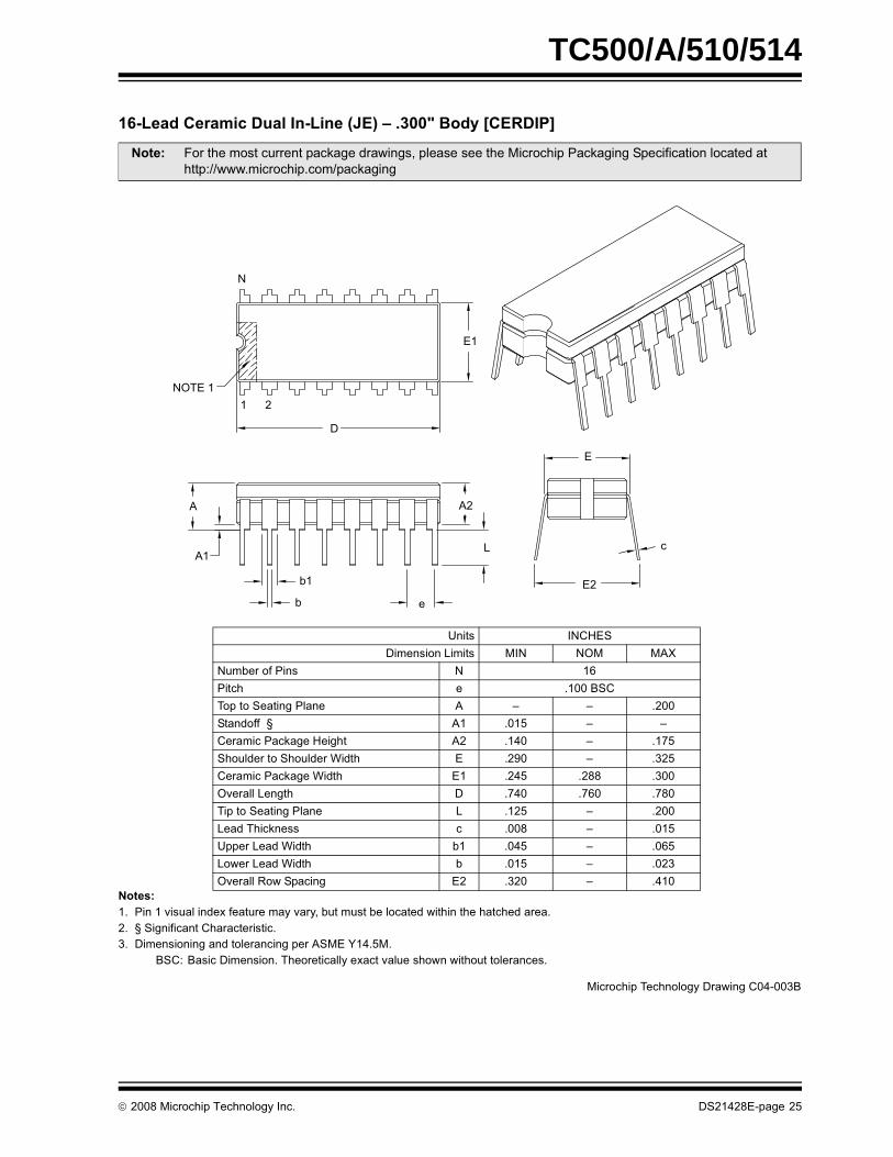
!"#
$%&' !"#$%!&'(!%&! %(%")%%%" *$%+% %, & "%-./
0+1 0 & %#%! ))%!%%
$%' 2%& %!%3") ' %3$%%"%%%144)))&&43
5% 6+7-& 8&% 6 69 :
6!&($ 6 ;% 0+ %% < < %"$$* / < <+&37% < /!"%!"="% - < ,/+&3="% - / >> ,98% ; > %% 8 / < 8" 3 > < /58"="% ( / < ;/8)8"="% ( / < ,9) - , <
N
NOTE 11 2
D
E1
E
c
E2
e
L
A2
b1
b
A1
A
) +,0
© 2008 Microchip Technology Inc. DS21428E-page 25
TC500/A/510/514
"&% " ""#
$%&' !"#$%!&'(!%&! %(%")%%%" *$%+% %, & "-"%!"&"$ %! "$ %! %#"? " & "%-./
0+1 0 & %#%! ))%!%%
$%' 2%& %!%3") ' %3$%%"%%%144)))&&43
5% 6+7-& 8&% 6 69 :
6!&($ 6 ;% 0+ %% < < ""3 3 / , /0 %% / < <!"%!"="% - , ,/""3="% - / >98% ,/ // / %% 8 / , /8" 3 > /58"="% ( / ; 8)8"="% ( > 9)* 0 < < ,
N
E1NOTE 1
D
1 2 3
A
A1 b1
b e
L
A2
E
eB
c
) +0
DS21428E-page 26 © 2008 Microchip Technology Inc.
TC500/A/510/514
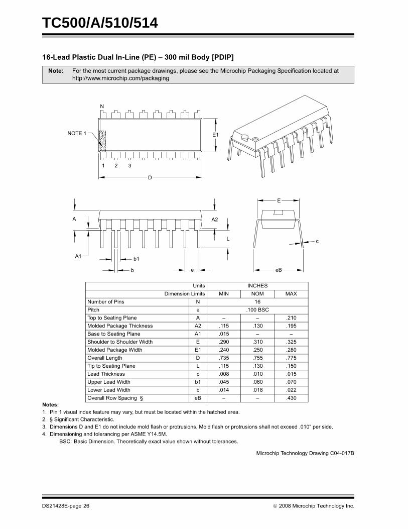
"&% ()% )* +,- ()#
$%&' !"#$%!&'(!%&! %(%")%%%" *$%+% %, & "-"%!"&"$ %! "$ %! %#"/&& " & "%-./
0+1 0 & %#%! ))%!%% -21 $& '! !)%!%%'$$&%!
$%' 2%& %!%3") ' %3$%%"%%%144)))&&43
5% 88- -& 8&% 6 69 :
6!&($ 6 ;% 0+97% < < ;/""3 3 / < <%"$$* < ,9="% - ,0+""3="% - /0+98% ,0++&$@%A / < /2%8% 8 < 2%% 8 -22% B < >B8" 3 < ,,8"="% ( , < /"$% /B < /B"$%0%%& /B < /B
D
N
E
E1
NOTE 1
1 2 3
be
A
A1
A2
L
L1
c
hh
φ
β
α
) +0
© 2008 Microchip Technology Inc. DS21428E-page 27

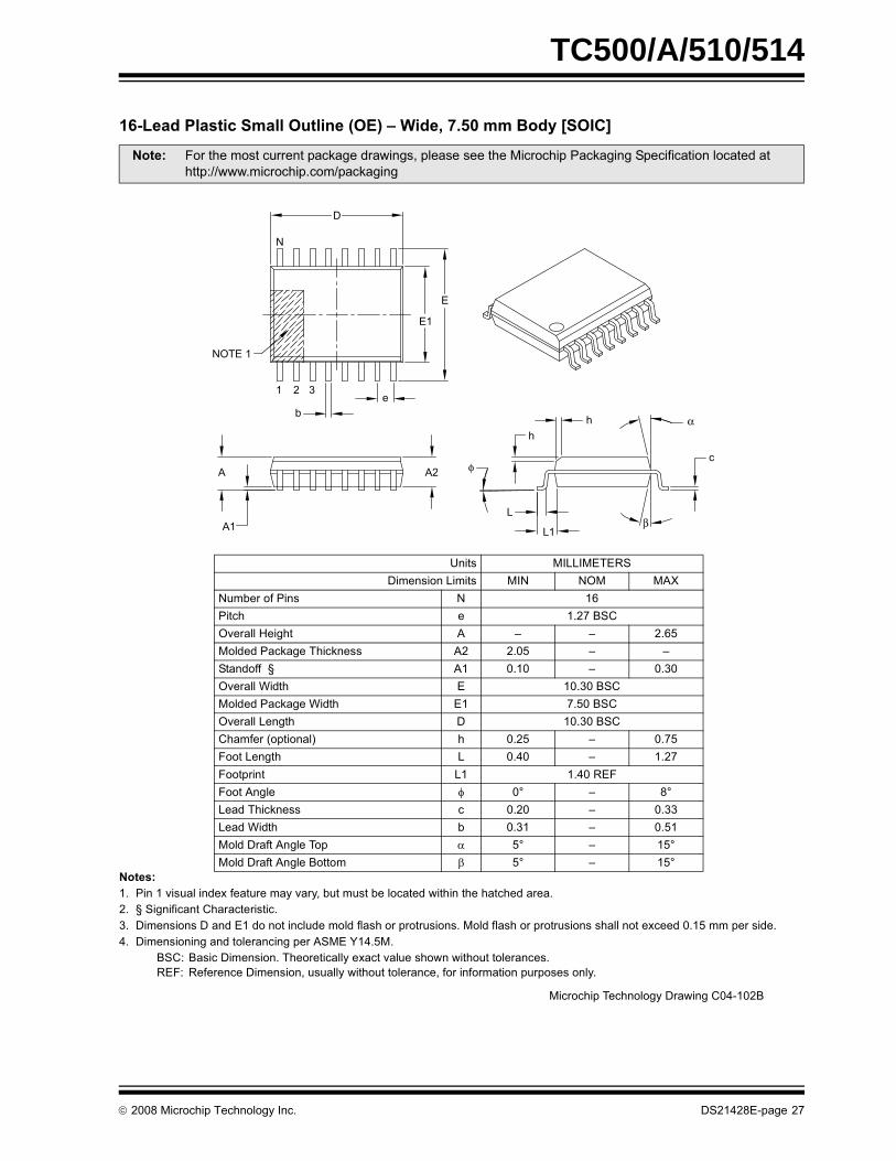
TC500/A/510/514
"&% ()% )* +,- ()#"%%
$%' 2%& %!%3") ' %3$%%"%%%144)))&&43
DS21428E-page 28 © 2008 Microchip Technology Inc.
TC500/A/510/514
./(0 "&% "1 (""#
$%&' !"#$%!&'(!%&! %(%")%%%" *$%+% %, & "-"%!"&"$ %! "$ %! %#"? " & "%-./
0+1 0 & %#%! ))%!%%
$%' 2%& %!%3") ' %3$%%"%%%144)))&&43
5% 6+7-& 8&% 6 69 :
6!&($ 6 % 0+ %% < < ""3 3 / , /0 %% / < <!"%!"="% - > , ,/""3="% - / >98% // / > %% 8 / , ;8" 3 > /58"="% ( / ; 8)8"="% ( > ,9)* 0 < < ,
N
E1NOTE 1
D
1 2 3
E
eB
c
A2
L
eb1
b
A
A1
) +,0
© 2008 Microchip Technology Inc. DS21428E-page 29
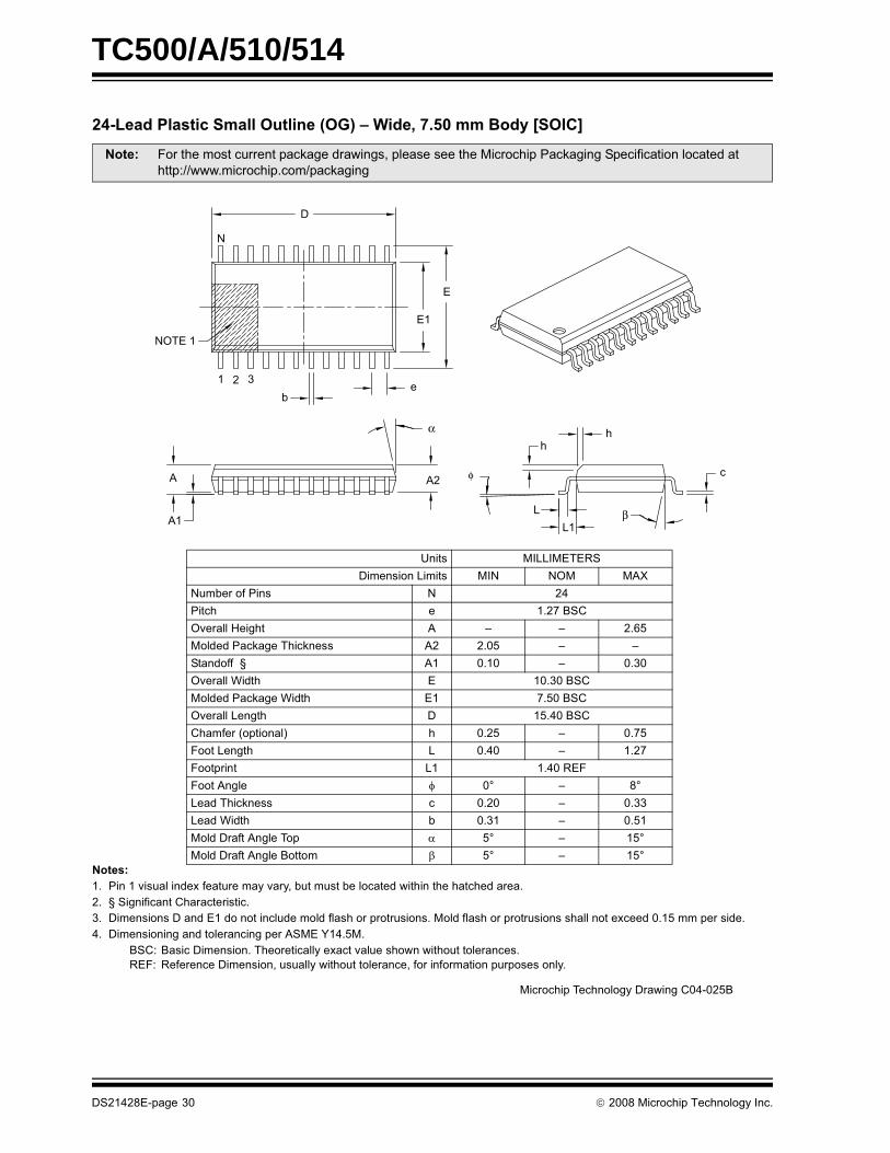
TC500/A/510/514
./"&% ()% OG* +,- ()#
$%&' !"#$%!&'(!%&! %(%")%%%" *$%+% %, & "-"%!"&"$ %! "$ %! %#"/&& " & "%-./
0+1 0 & %#%! ))%!%% -21 $& '! !)%!%%'$$&%!
$%' 2%& %!%3") ' %3$%%"%%%144)))&&43
5% 88- -& 8&% 6 69 :
6!&($ 6 % 0+97% < < ;/""3 3 / < <%"$$* < ,9="% - ,0+""3="% - /0+98% /0++&$@%A / < /2%8% 8 < 2%% 8 -22% B < >B8" 3 < ,,8"="% ( , < /"$% /B < /B"$%0%%& /B < /B
D
N
E
E1
NOTE 1
1 2 3b
e
A
A1
A2
hh
c
LL1
α
β
φ
) +/0
DS21428E-page 30 © 2008 Microchip Technology Inc.
TC500/A/510/514
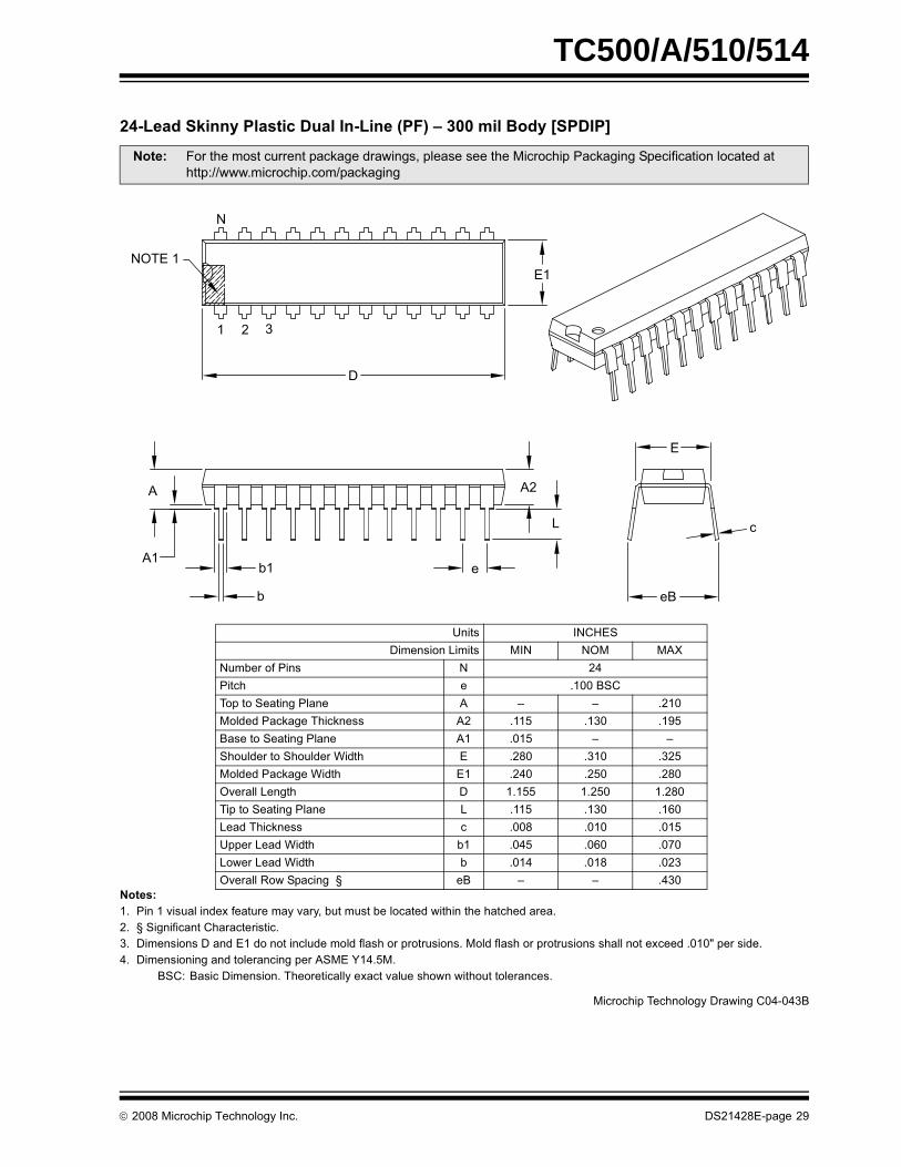
.2(0 "&% " (""#
$%&' !"#$%!&'(!%&! %(%")%%%" *$%+% %, & "-"%!"&"$ %! "$ %! %#"? " & "%-./
0+1 0 & %#%! ))%!%%
$%' 2%& %!%3") ' %3$%%"%%%144)))&&43
5% 6+7-& 8&% 6 69 :
6!&($ 6 >% 0+ %% < < ""3 3 ,/ /0 %% / < <!"%!"="% - , ,,/""3="% - >/ /98% ,/ ,;/ %% 8 , /8" 3 > /58"="% ( / 8)8"="% ( > 9)* 0 < < ,
NOTE 1
N
1 2
D
E1
eB
c
E
L
A2
eb
b1A1
A
3
) +0
© 2008 Microchip Technology Inc. DS21428E-page 31

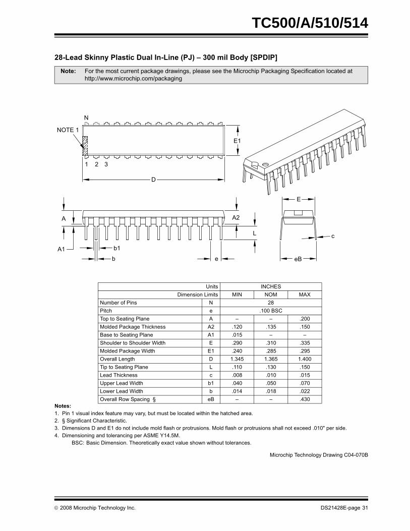
TC500/A/510/514
.2"&% ()% )* +,- ()#
$%&' !"#$%!&'(!%&! %(%")%%%" *$%+% %, & "-"%!"&"$ %! "$ %! %#"/&& " & "%-./
0+1 0 & %#%! ))%!%% -21 $& '! !)%!%%'$$&%!
$%' 2%& %!%3") ' %3$%%"%%%144)))&&43
5% 88- -& 8&% 6 69 :
6!&($ 6 >% 0+97% < < ;/""3 3 / < <%"$$* < ,9="% - ,0+""3="% - /0+98% 0++&$@%A / < /2%8% 8 < 2%% 8 -22% B < >B8" 3 > < ,,8"="% ( , < /"$% /B < /B"$%0%%& /B < /B
c
hh
LL1
A2
A1
A
NOTE 1
1 2 3
be
EE1
D
φ
β
α
N
) +/0
DS21428E-page 32 © 2008 Microchip Technology Inc.
TC500/A/510/514
APPENDIX A: REVISION HISTORY
Revision E (November 2008)• Updated Section 10.0 “Packaging Informa-
tion”.
Revision D (January 2006)• Undocumented changes.
Revision C (January 2004)• Undocumented changes.
Revision B (May 2002)• Undocumented changes.
Revision A (March 2001)• Initial release of this document.
© 2008 Microchip Technology Inc. DS21428E-page 33

TC500/A/510/514
NOTES:DS21428E-page 34 © 2008 Microchip Technology Inc.
TC500/A/510/514
PRODUCT IDENTIFICATION SYSTEMTo order or obtain information, e.g., on pricing or delivery, refer to the factory or the listed sales office.
PART NO. X /XX
PackageTemperatureRange
Device
Device TC500 16 Bit Analog ProcessorTC500A 16 Bit Analog ProcessorTC510 Precision Analog Front EndTC514 Precision Analog Front End
Temperature Range C = 0°C to +70°C (Commercial) I = 25°C to +85°C (Industrial)
Package JE = Ceramic Dual In-line, (300 mil Body), 16-leadPE = Plastic DIP, (300 mil Body), 16-leadOE = Plastic SOIC, (300 mil Body), 16-leadOE713 = Plastic SOIC, (300 mil Body), 16-lead
(Tape and Reel)PF = Plastic DIP, (300 mil Body), 24-leadOG = Plastic SOIC, (300 mil Body), 24-leadOG713 = Plastic SOIC, (300 mil Body), 24-lead
(Tape and Reel)PJ = Plastic DIP, (300 mil Body), 28-leadOI = Plastic SOIC, (300 mil Body), 28-leadOI713 = Plastic SOIC, (300 mil Body), 28-lead
(Tape and Reel)
Examples:a) TC500ACOE: Commercial Temp.,
16LD SOIC package.b) TC500ACOE713: Commercial Temp.,
16LD SOIC package,Tape and Reel.
c) TC500ACPE: Commercial Temp., 16LD PDIP package.
d) TC500AIJE: Industrial Temp., 16LD CERDIP package.
a) TC500COE: Commercial Temp., 16LD SOIC package.
b) TC500COE713: Commercial Temp., 16LD SOIC package,Tape and Reel.
c) TC500CPE: Commercial Temp., 16LD PDIP package.
d) TC500IJE: Industrial Temp., 16LD CERDIP package.
a) TC510COG: Commercial Temp., 24LD PDIP package.
b) TC510COG713: Commercial Temp., 24LD PDIP package, Tape and Reel.
c) TC510CPF: Commercial Temp., 24LD PDIP package.
a) TC514COI: Commercial Temp., 28LD PDIP package.
b) TC514COI713: Commercial Temp., 28LD PDIP package, Tape and Reel.
c) TC514CPJ: Commercial Temp., 28LD PDIP package.
© 2008 Microchip Technology Inc. DS21428E-page 35
TC500/A/510/514
NOTES:DS21428E-page 36 © 2008 Microchip Technology Inc.

Note the following details of the code protection feature on Microchip devices:• Microchip products meet the specification contained in their particular Microchip Data Sheet.
• Microchip believes that its family of products is one of the most secure families of its kind on the market today, when used in the intended manner and under normal conditions.
• There are dishonest and possibly illegal methods used to breach the code protection feature. All of these methods, to our knowledge, require using the Microchip products in a manner outside the operating specifications contained in Microchip’s Data Sheets. Most likely, the person doing so is engaged in theft of intellectual property.
• Microchip is willing to work with the customer who is concerned about the integrity of their code.
• Neither Microchip nor any other semiconductor manufacturer can guarantee the security of their code. Code protection does not mean that we are guaranteeing the product as “unbreakable.”
Code protection is constantly evolving. We at Microchip are committed to continuously improving the code protection features of ourproducts. Attempts to break Microchip’s code protection feature may be a violation of the Digital Millennium Copyright Act. If such actsallow unauthorized access to your software or other copyrighted work, you may have a right to sue for relief under that Act.
Information contained in this publication regarding deviceapplications and the like is provided only for your convenienceand may be superseded by updates. It is your responsibility toensure that your application meets with your specifications.MICROCHIP MAKES NO REPRESENTATIONS ORWARRANTIES OF ANY KIND WHETHER EXPRESS ORIMPLIED, WRITTEN OR ORAL, STATUTORY OROTHERWISE, RELATED TO THE INFORMATION,INCLUDING BUT NOT LIMITED TO ITS CONDITION,QUALITY, PERFORMANCE, MERCHANTABILITY ORFITNESS FOR PURPOSE. Microchip disclaims all liabilityarising from this information and its use. Use of Microchipdevices in life support and/or safety applications is entirely atthe buyer’s risk, and the buyer agrees to defend, indemnify andhold harmless Microchip from any and all damages, claims,suits, or expenses resulting from such use. No licenses areconveyed, implicitly or otherwise, under any Microchipintellectual property rights.
© 2008 Microchip Technology Inc.
Trademarks
The Microchip name and logo, the Microchip logo, Accuron, dsPIC, KEELOQ, KEELOQ logo, MPLAB, PIC, PICmicro, PICSTART, rfPIC, SmartShunt and UNI/O are registered trademarks of Microchip Technology Incorporated in the U.S.A. and other countries.
FilterLab, Linear Active Thermistor, MXDEV, MXLAB, SEEVAL, SmartSensor and The Embedded Control Solutions Company are registered trademarks of Microchip Technology Incorporated in the U.S.A.
Analog-for-the-Digital Age, Application Maestro, CodeGuard, dsPICDEM, dsPICDEM.net, dsPICworks, dsSPEAK, ECAN, ECONOMONITOR, FanSense, In-Circuit Serial Programming, ICSP, ICEPIC, Mindi, MiWi, MPASM, MPLAB Certified logo, MPLIB, MPLINK, mTouch, PICkit, PICDEM, PICDEM.net, PICtail, PIC32 logo, PowerCal, PowerInfo, PowerMate, PowerTool, REAL ICE, rfLAB, Select Mode, Total Endurance, WiperLock and ZENA are trademarks of Microchip Technology Incorporated in the U.S.A. and other countries.
SQTP is a service mark of Microchip Technology Incorporated in the U.S.A.
All other trademarks mentioned herein are property of their respective companies.
© 2008, Microchip Technology Incorporated, Printed in the U.S.A., All Rights Reserved.
Printed on recycled paper.
DS21428E-page 37
Microchip received ISO/TS-16949:2002 certification for its worldwide headquarters, design and wafer fabrication facilities in Chandler and Tempe, Arizona; Gresham, Oregon and design centers in California and India. The Company’s quality system processes and procedures are for its PIC® MCUs and dsPIC® DSCs, KEELOQ® code hopping devices, Serial EEPROMs, microperipherals, nonvolatile memory and analog products. In addition, Microchip’s quality system for the design and manufacture of development systems is ISO 9001:2000 certified.

DS21428E-page 38 © 2008 Microchip Technology Inc.
AMERICASCorporate Office2355 West Chandler Blvd.Chandler, AZ 85224-6199Tel: 480-792-7200 Fax: 480-792-7277Technical Support: http://support.microchip.comWeb Address: www.microchip.comAtlantaDuluth, GA Tel: 678-957-9614 Fax: 678-957-1455BostonWestborough, MA Tel: 774-760-0087 Fax: 774-760-0088ChicagoItasca, IL Tel: 630-285-0071 Fax: 630-285-0075DallasAddison, TX Tel: 972-818-7423 Fax: 972-818-2924DetroitFarmington Hills, MI Tel: 248-538-2250Fax: 248-538-2260KokomoKokomo, IN Tel: 765-864-8360Fax: 765-864-8387Los AngelesMission Viejo, CA Tel: 949-462-9523 Fax: 949-462-9608Santa ClaraSanta Clara, CA Tel: 408-961-6444Fax: 408-961-6445TorontoMississauga, Ontario, CanadaTel: 905-673-0699 Fax: 905-673-6509
ASIA/PACIFICAsia Pacific OfficeSuites 3707-14, 37th FloorTower 6, The GatewayHarbour City, KowloonHong KongTel: 852-2401-1200Fax: 852-2401-3431Australia - SydneyTel: 61-2-9868-6733Fax: 61-2-9868-6755China - BeijingTel: 86-10-8528-2100 Fax: 86-10-8528-2104China - ChengduTel: 86-28-8665-5511Fax: 86-28-8665-7889China - Hong Kong SARTel: 852-2401-1200 Fax: 852-2401-3431China - NanjingTel: 86-25-8473-2460Fax: 86-25-8473-2470China - QingdaoTel: 86-532-8502-7355Fax: 86-532-8502-7205China - ShanghaiTel: 86-21-5407-5533 Fax: 86-21-5407-5066China - ShenyangTel: 86-24-2334-2829Fax: 86-24-2334-2393China - ShenzhenTel: 86-755-8203-2660 Fax: 86-755-8203-1760China - WuhanTel: 86-27-5980-5300Fax: 86-27-5980-5118China - XiamenTel: 86-592-2388138 Fax: 86-592-2388130China - XianTel: 86-29-8833-7252Fax: 86-29-8833-7256China - ZhuhaiTel: 86-756-3210040 Fax: 86-756-3210049
ASIA/PACIFICIndia - BangaloreTel: 91-80-4182-8400 Fax: 91-80-4182-8422India - New DelhiTel: 91-11-4160-8631Fax: 91-11-4160-8632India - PuneTel: 91-20-2566-1512Fax: 91-20-2566-1513Japan - YokohamaTel: 81-45-471- 6166 Fax: 81-45-471-6122Korea - DaeguTel: 82-53-744-4301Fax: 82-53-744-4302Korea - SeoulTel: 82-2-554-7200Fax: 82-2-558-5932 or 82-2-558-5934Malaysia - Kuala LumpurTel: 60-3-6201-9857Fax: 60-3-6201-9859Malaysia - PenangTel: 60-4-227-8870Fax: 60-4-227-4068Philippines - ManilaTel: 63-2-634-9065Fax: 63-2-634-9069SingaporeTel: 65-6334-8870Fax: 65-6334-8850Taiwan - Hsin ChuTel: 886-3-572-9526Fax: 886-3-572-6459Taiwan - KaohsiungTel: 886-7-536-4818Fax: 886-7-536-4803Taiwan - TaipeiTel: 886-2-2500-6610 Fax: 886-2-2508-0102Thailand - BangkokTel: 66-2-694-1351Fax: 66-2-694-1350
EUROPEAustria - WelsTel: 43-7242-2244-39Fax: 43-7242-2244-393Denmark - CopenhagenTel: 45-4450-2828 Fax: 45-4485-2829France - ParisTel: 33-1-69-53-63-20 Fax: 33-1-69-30-90-79Germany - MunichTel: 49-89-627-144-0 Fax: 49-89-627-144-44Italy - Milan Tel: 39-0331-742611 Fax: 39-0331-466781Netherlands - DrunenTel: 31-416-690399 Fax: 31-416-690340Spain - MadridTel: 34-91-708-08-90Fax: 34-91-708-08-91UK - WokinghamTel: 44-118-921-5869Fax: 44-118-921-5820
WORLDWIDE SALES AND SERVICE
01/02/08
Related Documents