2/5/2010 1 Power Semiconductor Switches Pekik Argo Dahono Power Semiconductor Switches • Diodes (Uncontrolled switches) • Thyristors (Controllable at turn-on but uncontrolled at turn-off or commonly called as latched devices). Triac is under the same category. • BJT, MOSFET, IGBT, GTO, MCT etc. are fully controllable switches. Pekik A. Dahono -- Elektronika Daya 2

Welcome message from author
This document is posted to help you gain knowledge. Please leave a comment to let me know what you think about it! Share it to your friends and learn new things together.
Transcript

2/5/2010
1
Power Semiconductor Switches
Pekik Argo Dahono
Power Semiconductor Switches
• Diodes (Uncontrolled switches)
• Thyristors (Controllable at turn-on but
uncontrolled at turn-off or commonly called
as latched devices). Triac is under the same
category.
• BJT, MOSFET, IGBT, GTO, MCT etc. are
fully controllable switches.
Pekik A. Dahono -- Elektronika Daya 2

2/5/2010
2
Power Diodes
A
K
P
N
A
K
P
N
−N
A
K
AKv
AKi
AKv
AKi
Pekik A. Dahono -- Elektronika Daya 3
Reverse Recovery Problems
dE FD
S
oI
rrt
SI
oI
FDI
FDV
Pekik A. Dahono -- Elektronika Daya 4

2/5/2010
3
Power diodes
Diodes are classified as:
- general purpose or line-frequency diodes
- Fast recovery diodes
- Schottky diodes
Pekik A. Dahono -- Elektronika Daya 5
Schottky Diode
• The schottky diode has a smaller voltage
drop compared to conventional diodes
(about 0.3 V).
• The schottky diode has a smaller voltage
breakdown than conventional diodes (less
than 200 V).
Pekik A. Dahono -- Elektronika Daya 6

2/5/2010
4
Sample of diodes
Pekik A. Dahono -- Elektronika Daya 7
Thyristor
P
P
N
N
K
G
A
Ai
AKv
Ai
Pekik A. Dahono -- Elektronika Daya 8

2/5/2010
5
Thyristor Model
GI
1Q
2Q
1BI1EA II =
2CI 1CI
2BI
2EI
( )21
02012
02222
01111
1 αα
α
α
α
+−
++=
+−=
+−=
CCGA
CEC
CEC
IIII
III
III
Pekik A. Dahono -- Elektronika Daya 9
Thyristor in Simple Circuit
Pekik A. Dahono -- Elektronika Daya 10
• For successful turn-off, reverse voltage required for an
interval greater than the turn-off interval

2/5/2010
6
Thyristor Classification
• Phase control thyristors
• Inverter-grade or fast-type thyristors
• Light activated thyristors
• Reverse conducting thyristors
Pekik A. Dahono -- Elektronika Daya 11
Thyristor Features
• Latching devices
• Double carrier devices
• Having forward and reverse blocking
capabilities
• Very high gain (IA/Ig)
• Low on-state voltage
• Can be protected by fuse
Pekik A. Dahono -- Elektronika Daya 12

2/5/2010
7
Sample of thyristors
Pekik A. Dahono -- Elektronika Daya 13
Thyristor Modules
Pekik A. Dahono -- Elektronika Daya 14

2/5/2010
8
Snubbers for Diodes and Thyristors
• Maximum dv/dt across diodes or thyristors
must be limited and can be done by using an
RC snubber that is connected in parallel to
the devices.
• Maximum di/dt through diodes or thyristors
must be limited and can be done by using an
inductor that is connected in series to the
devices.
Pekik A. Dahono -- Elektronika Daya 15
Switching Characteristics
dont
ritfvt dofft
rvtfit
signal
Gate
current
& voltage
Transistor
power
Transistor
TvTi
dEoI
sonodson tIEW2
1=
soffodsoff tIEW2
1=
cdP
fvrison ttt += firvsoff ttt +=
dETi
Tv
oI
Pekik A. Dahono -- Elektronika Daya 16

2/5/2010
9
Desired Switch Characteristics
• Small leakage current in the off state
• Small on-state voltage
• Short turn-on and turn-off times
• Large forward and reverse blocking voltage capabilities
• High on-state current rating
• Positive temperature coefficient of on-state resistance
• Small control power
• Wide Safe Operating Area
• Large dv/dt and di/dt ratings
Pekik A. Dahono -- Elektronika Daya 17
Safe Operating Area
v
i
off-turn
on-turn
Pekik A. Dahono -- Elektronika Daya 18

2/5/2010
10
Losses
Switching losses :
Conduction losses :
( )soffsonsods ttfIEP +=21
s
ONooncd
T
TIVP =
fs is switching frequency.
Ts is switching period.
Pekik A. Dahono -- Elektronika Daya 19
Bipolar Junction Transistor
N
PN
C
E
BB
C
E
Ci
Bi
CEv
Ci
01 =Bi2Bi3Bi4Bi5Bi
12345 BBBBB iiiii >>>>
CEv
Ci
Pekik A. Dahono -- Elektronika Daya 20
• Used commonly in the past
• Now used in specific applications
• Replaced by MOSFETs and IGBTs

2/5/2010
11
VI characteristics of BJT
CEv
CI
00 =BI
1BI
2BI3BI4BI
5BI
0<BI
SUSBV 0CBBV
breakdown Second
breakdown
Primary
saturation-Quasisaturation-Hard
Pekik A. Dahono -- Elektronika Daya 21
Operating region
• Hard-saturation provides low voltage-drop but a
large storage time (turn-off time)
• Quasi-saturation provides high voltage-drop but a
small storage time.
• Second breakdown must be avoided by using a
snubber and proper base current control.
• Negative base current results in higher voltage
breakdown.
Pekik A. Dahono -- Elektronika Daya 22

2/5/2010
12
Antisaturation circuit
C
E
B'B
1D
2D
3D
Pekik A. Dahono -- Elektronika Daya 23
BJT Features
• Current controlled devices
• Double carrier devices
• No reverse blocking capability
• Low gain (Ic/Ib)
• Low on-state voltage
• Can not be protected by fuse
• Second breakdown problem
Pekik A. Dahono -- Elektronika Daya 24

2/5/2010
13
Darlington Configuration
Pekik A. Dahono -- Elektronika Daya 25
MOSFET
Di
01 =GSv2GSv3GSv4GSv5GSv
12345 GSGSGSGSGS vvvvv >>>>
DSv
Di
G
D
S
Di
DSv
Pekik A. Dahono -- Elektronika Daya 26
2/5/2010
14
MOSFET Features
• Voltage controlled devices
• Single carrier devices
• High on-state voltage
• Very high gain
• No reverse blocking capability
• No second breakdown problem
• Can not be protected by fuse
Pekik A. Dahono -- Elektronika Daya 27
Integrated Power MOSFET
Pekik A. Dahono -- Elektronika Daya 28

2/5/2010
15
Gate-Turn-Off (GTO) Thyristor
AKv
Ai
condition
Blocking
Pekik A. Dahono -- Elektronika Daya 29
GTO switching characteristic
IGR
(b)
Vd
Anodecurrent
Anodevoltage
Tail
current
Spikevoltage
IA
0Time
Pekik A. Dahono -- Elektronika Daya 30

2/5/2010
16
Turn-Off Snubber for GTO
Pekik A. Dahono -- Elektronika Daya 31
GTO Features
• Controllable at turn-on and turn-off
• High-voltage capability
• Can be designed with reverse blocking
capabilty
• Low gain at turn-off
• Low on-state voltage
• High turn-off losses
Pekik A. Dahono -- Elektronika Daya 32

2/5/2010
17
GTO vs IGCT
Pekik A. Dahono -- Elektronika Daya 33
GTO vs IGCT
Pekik A. Dahono -- Elektronika Daya 34

2/5/2010
18
Insulated Gate Bipolar Transistors (IGBTs)
C
E
Ci
GCEv
Ci
12345 GEGEGEGEGE vvvvv >>>>
01 =GEv2GEv3GEv4GEv5GEv
Pekik A. Dahono -- Elektronika Daya 35
IGBT Features
• Combining the advantages of BJT and
MOSFET
• No reverse blocking capability
• No second breakdown
• High gain at turn on and turn off
Pekik A. Dahono -- Elektronika Daya 36

2/5/2010
19
IGBT vs IGCT
Pekik A. Dahono -- Elektronika Daya 37
Other Switching Devices
• Static Induction Transistor and Static Induction
Thyristor. The main problems are normally-on and
high conduction loss. The advantage is that the
speed is very high.
• MOS Controlled Thyristor. Combining the
advantages of MOSFET and Thyristor. Still under
development.
• IGCT (Integrated Gate Controlled Thyristor). This
is further development of GTOs.
Pekik A. Dahono -- Elektronika Daya 38
2/5/2010
20
Switching Device Development
THYRISTOR
GTO
BPT
10-1
10-1 100 101 102 104
101
102
103
104
P (k
VA
)
f (kHz)
1 9 8 0
HIG
H P
OW
ER
EASY D
RIV
EHIG
H FREQUENCY
1 9 9 0
THYRISTOR
103
104
10-1
10-1 100 101 102 104
102
P (k
VA
)
f (kHz)
105
101
GTO
BPT
MOS
IGBT
2 0 0 0
10-1
10-1 100 101 102 104
OPERATION FREQUENCY f (kHz)
105
MOS
106
103
104
102
CO
NT
RO
LL
AB
LE
PO
WE
R
P (k
VA
)
101
105
BPT
IGBT
MCT SI Thy
GTO
THYRISTOR
GTO : GATE TURN-OFF THYRISTOR
MCT : MOS CONTROLLED THYRISTOR
SI Thy : STATIC INDUCTION THYRISTOR
BPT : BIPOLAR POWER TRANSISTOR
IGBT : INSULATED GATE BIPOLAR TRANSISTOR
Pekik A. Dahono -- Elektronika Daya 39
Reverse Conducting and
Reverse Blocking Switching Devices
conducting Reverse blocking Reverse
Pekik A. Dahono -- Elektronika Daya 40

2/5/2010
21
Bidirectional Switches
Pekik A. Dahono -- Elektronika Daya 41
Switching devicesSwitch Ideal
switch eduncontroll onalUnidirecti
switch lledsemicontro onalUnidirecti
switch controlled fully conducting Reverse
switch lledsemicontro nalBidirectio
switch controlled fully blocking Reverse
switch controlled fully nalBidirectio
switch controlled fully conducting Reverse
Pekik A. Dahono -- Elektronika Daya 42

2/5/2010
22
Properties and Rating of
Semiconductor Power Switches
Switch Control signal
Control characteristic
Switching frequency
Voltage drop
Maximum voltage
rating
Maximum current
rating
Diode medium 6.5 kV 5 kA
SCR current trigger low medium 6 kV 4 kA
TRIAC current trigger medium 1 kV 50 A
GTO current trigger low medium 6.5 kV 4.5 kA
BJT current linear medium low 1.5 kV 1 kA
MOSFET voltage linear Very high high 1 kV 200 A
IGBT voltage linear high medium 3.5 kV 2 kA
Pekik A. Dahono -- Elektronika Daya 43
Properties of New MaterialsProperty Si GaAs 3C-SiC 6H-SiC Diamond
Bandgap at 300 K (eV)
1.12 1.43 2.2 2.9 5.5
Relative dielectric constant
11.8 12.8 9.7 10 5.5
Saturated drift velocity (cm/s)
1x10⁷
2x10⁷
2.5x10⁷
2.5x10⁷
2.7x10⁷
Thermal
conductivity (W/cm/oC
1.5 0.5 5.0 5.0 20
Maximum
operating temperature (K)
400 460 873 1240 1100
Melting
temperature (C)
1415 1238 Sublime>1800 Sublime>1800 Phase change
Electron mobility at 300 K (cm2/Vs)
1400 8500 1000 600 2200
Breakdown
electric field
(V/cm)
3x10⁵
4x10⁵
4x10⁶
4x10⁶
1x10⁷
Pekik A. Dahono -- Elektronika Daya 44
2/5/2010
23
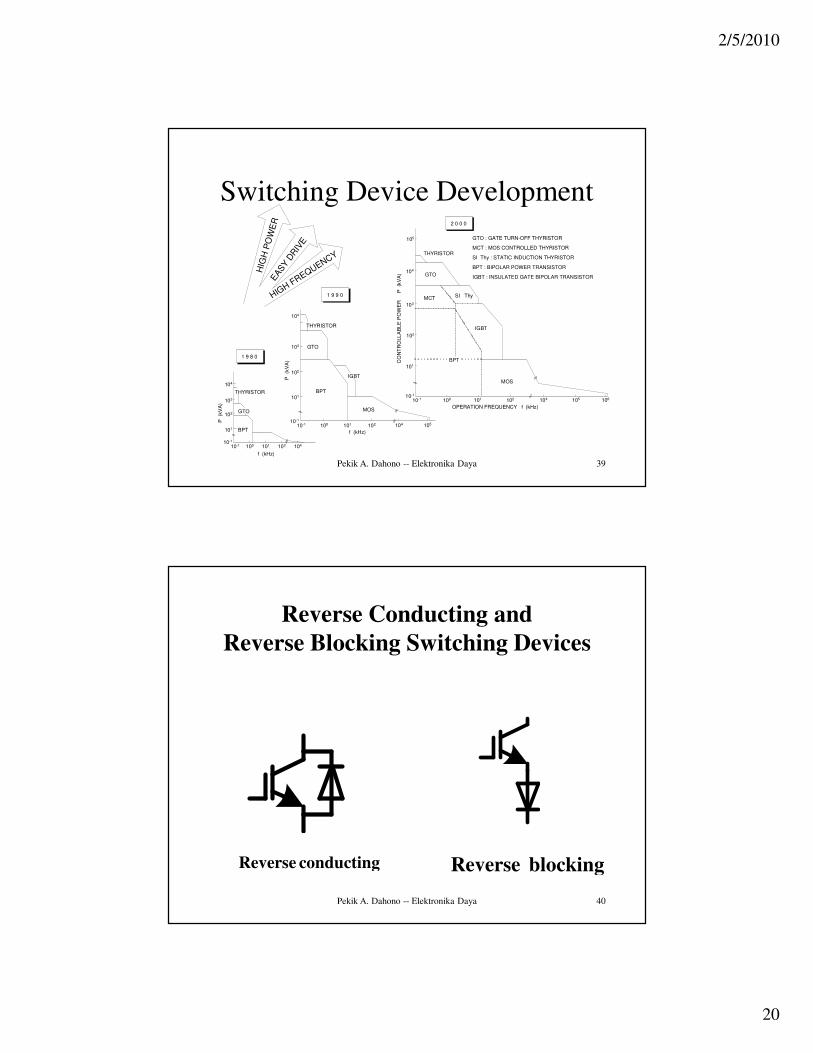
Applications
• Thyristor is only used for very large power applications.
• Forced commutated thyristors are no longer used.
• Bipolar junction transistors are no longer used.
• MOSFET is commonly used in low-power applications.
• IGBT is used from low-power up to medium power applications.
• GTO is used for large power applications.
Pekik A. Dahono -- Elektronika Daya 45
Loss Considerations
• Conduction losses
• Switching losses
• The loss will determine the junction temperature and the heatsink and cooler required.
• In many cases, the switching frequency is limited by the temperature instead of device speed.
Pekik A. Dahono -- Elektronika Daya 46

2/5/2010
24
Snubbers
• Turn-off losses can be reduced by using a turn-off snubber. This snubber is also useful to limit high dv/dt across the device.
• Turn-on losses can be reduced by using a turn-on snubber. This snubber is also useful to limit high di/dt through the device.
• Snubbers are useful to reduce the switching losses on the switching devices. The total switching losses, however, may still the same or even increase.
Pekik A. Dahono -- Elektronika Daya 47
Turn-ON and turn-OFF Snubbers
Pekik A. Dahono -- Elektronika Daya 48

2/5/2010
25
Reducing Switching Losses
• Switching losses can be reduced by using lossless snubbers. These snubbers, however, may make the converter circuit became complicated.
• IGBTs may operate without snubbers.
• GTOs and IGCTs usually need a turn-off snubber because of high tail current.
• Switching losses can be reduced or even eliminated by using soft-switching techniques. These methods, however, may increase the required voltage and/or current ratings.
Pekik A. Dahono -- Elektronika Daya 49
The End
Related Documents