J Electr Eng Technol Vol. 9, No. ?: 742-?, 2014 http://dx.doi.org/10.5370/JEET.2014.9.?.742 742 Power Loss Modeling of Individual IGBT and Advanced Voltage Balancing Scheme for MMC in VSC-HVDC System Gum Tae Son*, Soo Hyoung Lee** and Jung-Wook Park*** † Abstract –This paper presents the new power dissipation model of individual switching device in a high-level modular multilevel converter (MMC), which can be mostly used in voltage sourced converter (VSC) based high-voltage direct current (HVDC) system and flexible AC transmission system (FACTS). Also, the voltage balancing method based on sorting algorithm is newly proposed to advance the MMC functionalities by effectively adjusting switching variations of the sub-module (SM). The proposed power dissipation model does not fully calculate the average power dissipation for numerous switching devices in an arm module. Instead, it estimates the power dissipation of every switching element based on the inherent operational principle of SM in MMC. In other words, the power dissipation is computed in every single switching event by using the polynomial curve fitting model with minimum computational efforts and high accuracy, which are required to manage the large number of SMs. After estimating the value of power dissipation, the thermal condition of every switching element is considered in the case of external disturbance. Then, the arm modeling for high- level MMC and its control scheme is implemented with the electromagnetic transient simulation program. Finally, the case study for applying to the MMC based HVDC system is carried out to select the appropriate insulated-gate bipolar transistor (IGBT) module in a steady-state, as well as to estimate the proper thermal condition of every switching element in a transient state. Keywords: Advanced voltage balancing method, IGBT module, MMC, Polynomial curve fitting, power loss modeling, HVDC system 1. Introduction The modular multilevel converter (MMC) is the promising voltage source converter (VSC) topology for high-power application such as flexible AC transmission system (FACTS) and high-voltage direct current (HVDC) system [1]-[3]. It is characterized by stacks of identical half-bridge converter known as the sub-module (SM), which may have hundreds of levels, as shown in Fig. 1. In general, the SM has two switching devices realized by an anti-parallel connection of a fully controllable insulated- gate bipolar transistor (IGBT) and a diode to allow the reverse current. Each arm includes a protection converter reactor, L s , which can prevent overcurrent and balance capacitor voltage. By combining the capacitor voltages of SMs, the output voltage can be produced. This MMC topology has many advantages over the conventional VSCs [4]. In other words, since its output voltage is almost sinusoidal, the capacity of a filter can be minimized or even eliminated. Also, because each arm operates as a controllable voltage source, the common DC bus capacitor is not necessary. Therefore, the system can recover rapidly after a disturbance. Moreover, the MMC topology is more reliable than the conventional VSC in that redundant operation is available with proper semiconductor † Corresponding Author: School of Electrical and Electronic Engi- neering, Yonsei University, Seoul, Korea. (jungpark@yonsei. ac.kr) * LS Industrial Systems Co. Ltd, Anyang-si, Gyeonggi-do 431-080, Korea. ([email protected]) ** School of Electrical and Computer Engineering, Georgia Institute of Technology, Atlanta, GA 30332, USA. ([email protected]) *** School of Electrical and Electronic Engineering, Yonsei University, Seoul, Korea. ([email protected]) Received: February 10, 2013; Accepted: March 27, 2014 ISSN(Print) 1975-0102 ISSN(Online) 2093-7423 Fig. 1. The configuration of MMC: (a) three-phase n-level MMC topology; (b) sub-module.

Welcome message from author
This document is posted to help you gain knowledge. Please leave a comment to let me know what you think about it! Share it to your friends and learn new things together.
Transcript

J Electr Eng Technol Vol. 9, No. ?: 742-?, 2014 http://dx.doi.org/10.5370/JEET.2014.9.?.742
742
Power Loss Modeling of Individual IGBT and Advanced Voltage Balancing Scheme for MMC in VSC-HVDC System
Gum Tae Son*, Soo Hyoung Lee** and Jung-Wook Park***†
Abstract –This paper presents the new power dissipation model of individual switching device in a high-level modular multilevel converter (MMC), which can be mostly used in voltage sourced converter (VSC) based high-voltage direct current (HVDC) system and flexible AC transmission system (FACTS). Also, the voltage balancing method based on sorting algorithm is newly proposed to advance the MMC functionalities by effectively adjusting switching variations of the sub-module (SM). The proposed power dissipation model does not fully calculate the average power dissipation for numerous switching devices in an arm module. Instead, it estimates the power dissipation of every switching element based on the inherent operational principle of SM in MMC. In other words, the power dissipation is computed in every single switching event by using the polynomial curve fitting model with minimum computational efforts and high accuracy, which are required to manage the large number of SMs. After estimating the value of power dissipation, the thermal condition of every switching element is considered in the case of external disturbance. Then, the arm modeling for high-level MMC and its control scheme is implemented with the electromagnetic transient simulation program. Finally, the case study for applying to the MMC based HVDC system is carried out to select the appropriate insulated-gate bipolar transistor (IGBT) module in a steady-state, as well as to estimate the proper thermal condition of every switching element in a transient state.
Keywords: Advanced voltage balancing method, IGBT module, MMC, Polynomial curve fitting, power loss modeling, HVDC system
1. Introduction The modular multilevel converter (MMC) is the
promising voltage source converter (VSC) topology for high-power application such as flexible AC transmission system (FACTS) and high-voltage direct current (HVDC) system [1]-[3]. It is characterized by stacks of identical half-bridge converter known as the sub-module (SM), which may have hundreds of levels, as shown in Fig. 1. In general, the SM has two switching devices realized by an anti-parallel connection of a fully controllable insulated-gate bipolar transistor (IGBT) and a diode to allow the reverse current. Each arm includes a protection converter reactor, Ls, which can prevent overcurrent and balance capacitor voltage. By combining the capacitor voltages of SMs, the output voltage can be produced. This MMC topology has many advantages over the conventional VSCs [4].
In other words, since its output voltage is almost sinusoidal, the capacity of a filter can be minimized or even eliminated. Also, because each arm operates as a controllable voltage source, the common DC bus capacitor is not necessary. Therefore, the system can recover rapidly after a disturbance. Moreover, the MMC topology is more reliable than the conventional VSC in that redundant operation is available with proper semiconductor
† Corresponding Author: School of Electrical and Electronic Engi-neering, Yonsei University, Seoul, Korea. (jungpark@yonsei. ac.kr)
* LS Industrial Systems Co. Ltd, Anyang-si, Gyeonggi-do 431-080, Korea. ([email protected])
** School of Electrical and Computer Engineering, Georgia Institute of Technology, Atlanta, GA 30332, USA. ([email protected])
*** School of Electrical and Electronic Engineering, Yonsei University, Seoul, Korea. ([email protected])
Received: February 10, 2013; Accepted: March 27, 2014
ISSN(Print) 1975-0102 ISSN(Online) 2093-7423
Fig. 1. The configuration of MMC: (a) three-phase n-level
MMC topology; (b) sub-module.
Gum Tae Son, Soo Hyoung Lee and Jung-Wook Park
743
devices [5]. As the level in MMC topology increases, more
switching devices are required such that they can operate independently according to their particular control actions. The actual operations for each switching device must ensure the design of reliable system in power grid planning. One important factor for this issue is the junction temperature of switching devices. Note that the tem-perature is mainly affected by the power dissipation due to its switching and conduction losses of device. In addition, many designers in industry are trying to maximize the capacity of device for cost reason [6]. The exact power loss modeling in each SM makes it possible to optimize its performance with the proper thermal management and packaging. However, considering many SMs with numerous switching devices in series and parallel, it is not feasible to evaluate the practical junction temperature and power loss of each device in the design stage. Instead, the preliminary and proper information obtained by simulation study can be preferably used.
There are several studies [6-10] for the power loss modeling of MMC. The previous work in [7] estimated the power dissipation in MMC with the simple functions derived from losses based on a typical switching waveform. However, this method requires several parameters, which are not easy to gather or derive from the datasheet. Furthermore, they are subject to change according to condition. In [8], the average power dissipation of MMC topology was analytically calculated based on the assumption that the system operates in only steady-state condition, but not in transient condition. Also, the switching physics of device were applied to achieve the exact loss calculation in [9]. However, it requires a very small simulation time step, and therefore may not be applicable for the high-level MMC topology.
To satisfy the practical requirements for accurate preliminary design work of high-level MMC, this study applies the polynomial curve fitting model, which is available with the datasheet provided from a manufacturer. Then, the switching mechanism of an individual SM depending on the variations of state and the arm current polarity is investigated to build the user-defined model for high-level MMC by using the power systems computer aided design/electromagnetic transients including DC (PSCAD/EMTDC®) software [11]. This paper makes the new contribution by developing the practical power loss modeling of individual switching device in each SM without regard to the number of SMs. Moreover, the power loss of overall system is estimated accurately. In particular, the proposed method can be an effective tool to verify the new modulation method or voltage balancing method because this work requires both the condition of individual SM state and the relationship between SMs in MMC arm. Therefore, the advanced voltage balancing method by adjusting the switching number is also proposed via the power loss modeling of MMC.
2. Modeling for High-Level MMC
2.1 Operating states of SM As mentioned in above, a common central capacitor is
not necessary in the MMC. Instead, each SM is considered to be a controllable voltage source, which can interface with the controller via a bi-directional optic cable [12]. The output voltage of converter can be implemented by adjusting the number of SMs in both arms. Therefore, the proper management of SMs becomes the important factor to operate the converter sustainably and reliably.
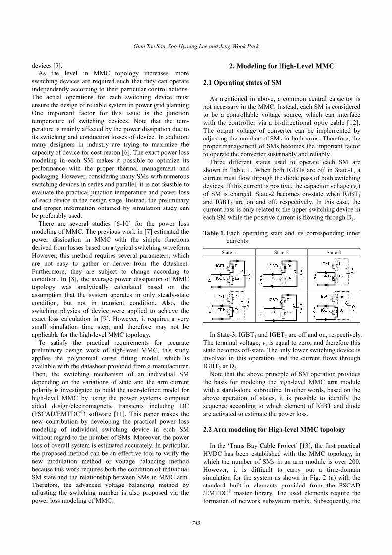
Three different states used to operate each SM are shown in Table 1. When both IGBTs are off in State-1, a current must flow through the diode pass of both switching devices. If this current is positive, the capacitor voltage (vc) of SM is charged. State-2 becomes on-state when IGBT1 and IGBT2 are on and off, respectively. In this case, the current pass is only related to the upper switching device in each SM while the positive current is flowing through D1.
Table 1. Each operating state and its corresponding inner
currents
State-1 State-2 State-3
In State-3, IGBT1 and IGBT2 are off and on, respectively.
The terminal voltage, vx is equal to zero, and therefore this state becomes off-state. The only lower switching device is involved in this operation, and the current flows through IGBT2 or D2.
Note that the above principle of SM operation provides the basis for modeling the high-level MMC arm module with a stand-alone subroutine. In other words, based on the above operation of states, it is possible to identify the sequence according to which element of IGBT and diode are activated to estimate the power loss.
2.2 Arm modeling for High-level MMC topology
In the ‘Trans Bay Cable Project’ [13], the first practical
HVDC has been established with the MMC topology, in which the number of SMs in an arm module is over 200. However, it is difficult to carry out a time-domain simulation for the system as shown in Fig. 2 (a) with the standard built-in elements provided from the PSCAD /EMTDC® master library. The used elements require the formation of network subsystem matrix. Subsequently, the

Power Loss Modeling of Individual IGBT and Advanced Voltage Balancing Scheme for MMC in VSC-HVDC System
744
calculation of its inverse in every switching event suffers severe computational efforts.
The switching elements such as IGBT or diode are equivalent to a resistor with two states in the simulation. Also, only one switching element of an IGBT and a diode, which are connected in antiparallel, is activated. Therefore, these switching devices can be represented by a pair of two resistors (i.e. R1 and R2 in the first SM), as depicted in Fig. 2 (b) [10]. These two resistors are determined according to the state of SM. Note that the values of R1 and R2 cannot be the same. Then, the capacitor of SM is modeled with the first-order differential equation, which can be calculated in every time step by using the trapezoidal integration method. Even though it is possible to apply the SMs with different values of capacitors, it is assumed that their values for all SMs are equal. When the j-th SM is considered, the corresponding capacitor voltage, vcj can be represented with the j-th history voltage source (vchj), the current flowing into the j-th SM (Icj), and a resistor (Rc) as
( ) ( )cj c cj chjv R I t v t t= + -D (1)
where Rc is ∆t/2C, ∆t is the simulation time step, and C is the capacitance. Based on the trapezoidal integration method, the history voltage source must be updated at every simulation time step. Because an arm of MMC consists of several SMs in series, the voltage of arm module is equal to the sum of terminal voltage, vx of individual SM, which can be computed with the given resistances and the history voltage source as
2 22
1 2 1 2
( ) 1 ( ) ( )xj chjc c
R Rv t R I t v t tR R R R R R
æ ö= - + -Dç ÷+ + + +è ø
(2)
As the result by adding (2) to all SMs, the arm module is
represented in the form of Thevenin equivalent equation. Then, it is transformed to another suitable form to interface with the network subsystem in the simulation. The PSCAD / EMTDC® software provides the stand-alone subroutine,
which can create a flexible programming environment for the user by using a branch-based interface command. In particular, the branch effectively characterizes the model subroutine as a Norton current source connected in parallel with an equivalent branch conductance [10]. Therefore, the Thevenin arm module is converted to the Norton equivalent circuit, and it is applied to form the stand-alone subroutine, as shown in Fig. 2 (c). It consists of three EMTDC internal variables, which are CCBR, GEQ, and EBR [11]. The CCBR is the Norton equivalent history current source, the GEQ is the equivalent conductance, and the EBR is the history voltage source.
Again, although the arm module of high-level MMC is organized with numerous SMs as shown in Fig. 2 (a), each SM can be represented as its equivalent circuit in Fig. 2 (b) by using the FORTRAN script in PSCAD/EMTDC® software. Then, the script is converted to the stand-alone subroutine shown in Fig. 2 (c) based on the Dommel’s algorithm [10]. The number of SM is scalable because it does not have the effect on computational requirement. At every simulation time step, all information in an arm is obtained, and the model can respond to individual control signal.
2.3 Control Scheme for MMC
In general, the control structure of MMC consists of
three control units as shown in Fig. 3 [12]. The supervisory control unit manages the entire system depending on its applications. It accommodates the inherent topological properties such as the capacitor voltage control for SM and the circulating current elimination. Also, it deals with the active and reactive power controls as well as the DC voltage control [4]. Then, the reference signal generated from the supervisory control unit is transmitted to the central control unit. Even though it is fully accomplished by one single modulator in this control unit, the modulation and voltage balancing controls are separately implemented. Firstly, the nearest level control (NLC) method with low frequency is used for the modulation control because it makes it possible for the process of independent comparison and easy implementation with less computational require-ment. As the result, the number of on-state SMs, non(t) is determined in each arm at every simulation time step. Then, the value of n-level converter is calculated by
1( )
2on roundx nn t fQæ ö -
= +ç ÷è ø
(3)
where x is the reference value, and Q is the voltage difference between the two levels. Moreover, x/Q is evaluated by using the round function, fround so that it becomes the integer close to a real number. Then, the sorting algorithm manages the voltage balancing of each SM. To implement this, the capacitor voltage of each SM
Fig. 2. (a) Structure of arm module; (b) equivalent circuit;
(c) stand-alone subroutine for arm module.

Gum Tae Son, Soo Hyoung Lee and Jung-Wook Park
745
must be monitored and kept to be equal. From the monitored voltage value and current polarity, the balancing problem can be solved by applying the sorting algorithm in Fig. 3. It simply sequences the SMs from the highest to the lowest capacitor voltage in an arm. Then, it selects the appropriate SMs at every time step based on the charging or discharging properties of SM, as already mentioned in Section 2.1. In other words, in the case of a positive arm current, the SM with the lowest voltage level is selected to charge its capacitor. In the case of a negative arm current, the SM with the highest voltage is chosen to supply the output voltage level by discharging.
Finally, the converter cubicle unit receives the cor-responding switching state and sends its inner information back to the central control unit.
2.4 Advanced voltage balancing method
The traditional voltage balancing method using only
capacitor voltage information makes the number of switching increased. From a single SM point of view, the traditional method does not have a merit of low modulation method. Therefore, it is necessary to reduce the number of switching method. Additionally, the number of switching needs to be adjustable depending on the system specification. Since the relationship between converter loss and capacitor rate in a given control method is contradictive, the designer of MMC should consider the number of switching.
In this paper, the advanced method based on the sorting algorithm is proposed by reducing the number of switching in each SM during one cycle of output voltage. In addition, this method can regulate the switching number of each SM evenly within the limited capacity of capacitor. The proposed voltage balancing algorithm is shown in Fig. 4. Firstly, it classifies total SMs into two groups (on-state and off-state) depending on the previous SM’s gate signal. Then, all SMs in each group are independently sorted in the descending order.
Based on two criteria, which are the polarity of current, i(t) in an arm and the difference value (Diff) of modulation between present (t) and previous (t-∆t) time steps, which group will be activated is determined. In other words,
when both the current polarity and the Diff are positive, the SMs with the lowest value of capacitor voltage in off-state group are turned on to charge the capacitors of corresponding SMs. In contrast, when the current polarity is still positive but the Diff is negative, the SMs with the highest value in on-state group are turned off to keep them within overcharging limit. Also, when i(t) < 0 and Diff > 0, the SMs with highest value in off-state group are turned on for charging the capacitor. Finally, when both criteria are negative, the SMs with the lowest value in on-state group are turned off to keep the continuous discharging operation within undercharging limit. The above four SM states depend on the results of varying modulation. According to the grouping method, the number of switching is dramatically reduced to only one or two changes during one cycle of system frequency.
Above grouping method has a limitation that is not afforded to adjust the switching number according to the MMC designer. The switching frequency of the MMC system is fixed and this reduces the freedom of control. The main idea of advanced voltage balancing method is interposition of switching flag during the above grouping method. The switching flag is status change of SMs in two different groups compulsory. As the result of advanced method, the ripple of capacitor voltage can be reduced in an intelligent manner. In other words, the identical number of SMs in off-state and on-state groups is compared by using the values of their capacitor voltages and interchanging states. For example, when both criteria are positive as shown in Fig. 4, two SMs with the lowest value in off-state group are firstly turned on. Then, the third SM with the lowest value in off-state group and the first SM with the highest value in on-state group are compared to each other. If the voltage of SM in off-state group is lower than that in on-state group, the states of
Fig. 3. Structure of MMC control
on
Lon-state H Loff-state
on
off
H Lon-state H Loff-state
off
HLon-state H Loff-stateH
Lon-state H Loff-stateH
Diff >0 and i >0 Diff >0 and i <0
Diff <0 and i >0 Diff <0 and i <0
Compare the voltages
Compare the voltages Compare the voltages
Compare the voltages
Classify all sub-modules into on-state, off-state groups.
Sort the on-state groupand the off-state groupeach other in a descending order
g (t- t)
vSM (t)
Diffnon(t- t)
Modulation Method
non(t)+
-
SMon-state
SMoff-stateMMC Arm Module
i (t)
Fig. 4. The proposed voltage balancing method
Power Loss Modeling of Individual IGBT and Advanced Voltage Balancing Scheme for MMC in VSC-HVDC System
746
these SMs are interchanged. The SM number in this forced process can be adjusted by the engineer for voltage balancing. In this case, even though the additional switching of SM might increase the power loss, it provides the cost-effective solution to reduce the voltage ripple.
3. Power Loss Modeling for High-Level MMC
3.1 Power loss modeling for arm module The power loss in a switching device consists of
conduction loss, blocking loss, and switching loss. The conduction loss is calculated by the product of current and forward saturation voltage of switch. The blocking loss is computed by the product of leakage current and blocking voltage. And, the switching loss is divided into turn-on and turn-off losses. In general, the forward saturation and blocking voltages can be directly obtained from the datasheet of switch device.
To this point, various methods have been investigated to estimate the switching loss, such as the loss modeling based on physics of device, the loss estimation derived from typical switching waveform, and the analytical average power loss calculation, etc. Even though they have many advantages, there are limitations to apply for this study. In other words, the loss modeling based on physics is not suitable to apply for the MMC because it requires very short simulation time step (i.e. a few hundred nanoseconds). In addition, the loss estimation derived from typical switching waveform requires many parameters, which are not easily obtained from the given datasheet. The analytical average power loss calculation cannot provide the power loss information of each SM. Note that the SM is subject to changing its states under various conditions. Moreover, its switching elements exhibit the hard switching resulting in high switching losses and stresses. Therefore, the new power loss modeling is proposed for the exact switching loss calculation with relatively less computational effort.
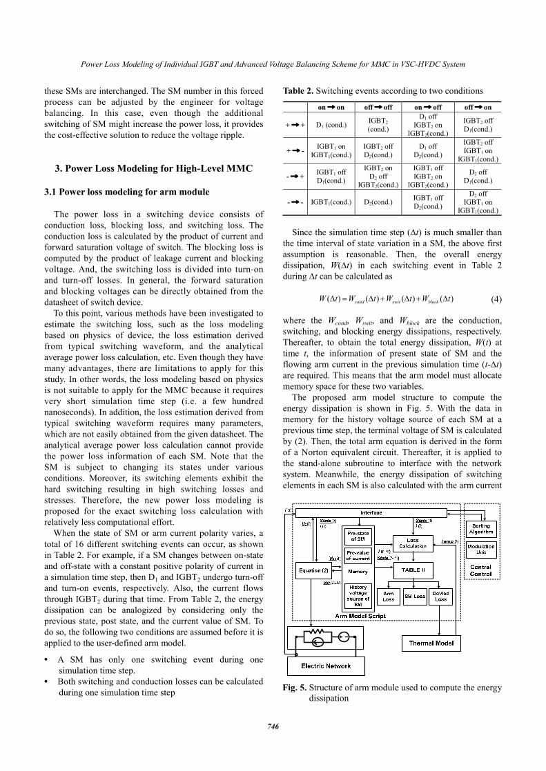
When the state of SM or arm current polarity varies, a total of 16 different switching events can occur, as shown in Table 2. For example, if a SM changes between on-state and off-state with a constant positive polarity of current in a simulation time step, then D1 and IGBT2 undergo turn-off and turn-on events, respectively. Also, the current flows through IGBT2 during that time. From Table 2, the energy dissipation can be analogized by considering only the previous state, post state, and the current value of SM. To do so, the following two conditions are assumed before it is applied to the user-defined arm model.
Ÿ A SM has only one switching event during one simulation time step.
Ÿ Both switching and conduction losses can be calculated during one simulation time step
Table 2. Switching events according to two conditions
on → on off → off on → off off → on
+ → + D1 (cond.) IGBT2
(cond.)
D1 off IGBT2 on
IGBT2(cond.)
IGBT2 off D1(cond.)
+ → - IGBT1 on IGBT1(cond.)
IGBT2 off D2(cond.)
D1 off D2(cond.)
IGBT2 off IGBT1 on
IGBT1(cond.)
- → + IGBT1 off D1(cond.)
IGBT2 on D2 off
IGBT2(cond.)
IGBT1 off IGBT2 on
IGBT2(cond.)
D2 off D1(cond.)
- → - IGBT1(cond.) D2(cond.) IGBT1 off D2(cond.)
D2 off IGBT1 on
IGBT1(cond.) Since the simulation time step (∆t) is much smaller than
the time interval of state variation in a SM, the above first assumption is reasonable. Then, the overall energy dissipation, W(∆t) in each switching event in Table 2 during ∆t can be calculated as
( ) ( ) ( ) ( )cond swit blockW t W t W t W tD = D + D + D (4)
where the Wcond, Wswit, and Wblock are the conduction, switching, and blocking energy dissipations, respectively. Thereafter, to obtain the total energy dissipation, W(t) at time t, the information of present state of SM and the flowing arm current in the previous simulation time (t-∆t) are required. This means that the arm model must allocate memory space for these two variables.
The proposed arm model structure to compute the energy dissipation is shown in Fig. 5. With the data in memory for the history voltage source of each SM at a previous time step, the terminal voltage of SM is calculated by (2). Then, the total arm equation is derived in the form of a Norton equivalent circuit. Thereafter, it is applied to the stand-alone subroutine to interface with the network system. Meanwhile, the energy dissipation of switching elements in each SM is also calculated with the arm current
Fig. 5. Structure of arm module used to compute the energy
dissipation
Gum Tae Son, Soo Hyoung Lee and Jung-Wook Park
747
and junction temperature. It includes the conduction loss (of IGBT and diode) and every switching loss (turn-on/turn-off losses of IGBT and turn-off loss of diode). With all information in pre- and post-states of SMs and their current polarity, it can be determined which switching elements of corresponding SMs are related to each other. Finally, the calculation of energy dissipation in each SM and arm module is straightforward at every time step. This is used as the input of dynamic thermal model, by which the temperatures in various layers of switching element can be also computed. More details for dynamic thermal model are explained in the Section 3.3.
3.2 Polynomial curve fitting model
From the proposed arm model in above, the state and
capacitor voltage of each SM can be observed in every simulation time step. Based on this information, the energy dissipation of switching elements must be calculated with the minimum computational requirement and high accuracy to deal with many SMs in an arm. For this objective, the polynomial curve fitting model [14-15] is applied. This method defines the energy dissipation with a function of current flowing into the switching element. In particular, if the datasheet of IGBT module is given based on the fixed value of capacitor voltage, this becomes the most suitable method for the exact modeling of high-level MMC. Firstly, the conduction loss, Pcond is calculated from the relationship between the forward saturation voltage and the corresponding current given in the datasheet. Then, based on the polynomial curve fitting model, it can be approximated by the second-order polynomial form as
2
1 2 3( ) ( )cond cj cjP a a I t a I t= + + (5)
where a1, a2, and a3 are coefficients derived from the fitting curve. As mentioned previously, the energy dissipation due to the conduction loss is simply computed by multiplying (5) with ∆t since the only one switching event occurs in one simulation time step.
Also, the switching loss is calculated in the similar manner. In general, the datasheet of IGBT module gives the information of switching loss based on the experimental analysis in half-bridge switching mode and inductive load condition. Because the SM operates under the same condition, the accurate switching loss can be computed for each switching element according to its structure characteristics. For example, the turn-on operation of IGBT mainly depends on its reverse recovery performance of antiparallel diode [16]. From the datasheet, the switching energy losses are approximated by the second-order polynomial fitting curves as
2
1 2 3
21 2 3
21 2 3
( ) ( )
( ) ( )
( ) ( )
ON cj cj
OFF cj cj
ref cj cj
E b b I t b I t
E c c I t c I t
E d d I t d I t
= + +
= + +
= + +
21 2 3
21 2 3
21 2 3
( ) ( )
( ) ( )
( ) ( )
ON cj cj
OFF cj cj
ref cj cj
E b b I t b I t
E c c I t c I t
E d d I t d I t
= + +
= + +
= + + (6)
where the bj and cj (j = 1, 2, 3) are coefficients of turn-on (EON) and turn-off (EOFF) energy dissipation curves of IGBT, respectively. And, the dj is coefficient of turn-off (Eref) energy dissipation curve of diode. Because the turn-on loss of diode is very small when compared to the turn-off loss [16], it is negligible. The estimation result from (6) is shown in Fig. 6 (b) with the comparison of experimental switching loss data. The second-order polynomial curve fitting model still shows the good performance.
3.3 Thermal model
The thermal model of switching element can be
represented as the electric circuit form. The values of i-th thermal resistance, Rthi and capacitance, Cthi depend on the layer number of semiconductor element mounted on the heat sink [17-18]. This can be performed by approximating the curve into the analytical function as
/( )
1( ) (1 )i
mt
th j c thii
Z t R e t--
=
= -å (7)
where τi is the time constant, Rthi /Cthi.
4. Evaluation of Performance
4.1 Case study for selection IGBT using power loss modeling
To evaluate the performance of proposed power
dissipation model, the simple system with the MMC connected between a DC voltage source (DC bus) and a three-phase resistive load is firstly considered. As in the Trans Bay Cable Project [13], the MMC is designed as the mono-polar structure with DC voltage of ± 200 kV, DC current of 1026 A, and three-phase resistive load of 400 MW. Three 120° phase-shifted sinusoidal signals are substituted as reference signals. The simulation time-step is 20 µs, and the plotting time-step is 200 µs.
The number of SMs in an arm is determined by considering three conditions, which are the voltage rating of IGBT module, the average capacitor voltage of SM, and the number of redundant SMs for system reliability [5]. Since the average capacitor voltage is normally recommended to be less than 50 to 60 % of the rated voltage of IGBT module [19], the first two conditions are closely related to each other. In this study, the Mitsubishi high voltage IGBT module of 4500 V is chosen as the commercially approved switching device. From this IGBT module, the average capacitor voltage is chosen to be 2.2 kV, which is similar to that of practical experiment to
Power Loss Modeling of Individual IGBT and Advanced Voltage Balancing Scheme for MMC in VSC-HVDC System
748
obtain the switching loss in its data sheet. On the other hand, it is assumed that redundant SMs are not added to the arm. Therefore, the number of SMs is 180.
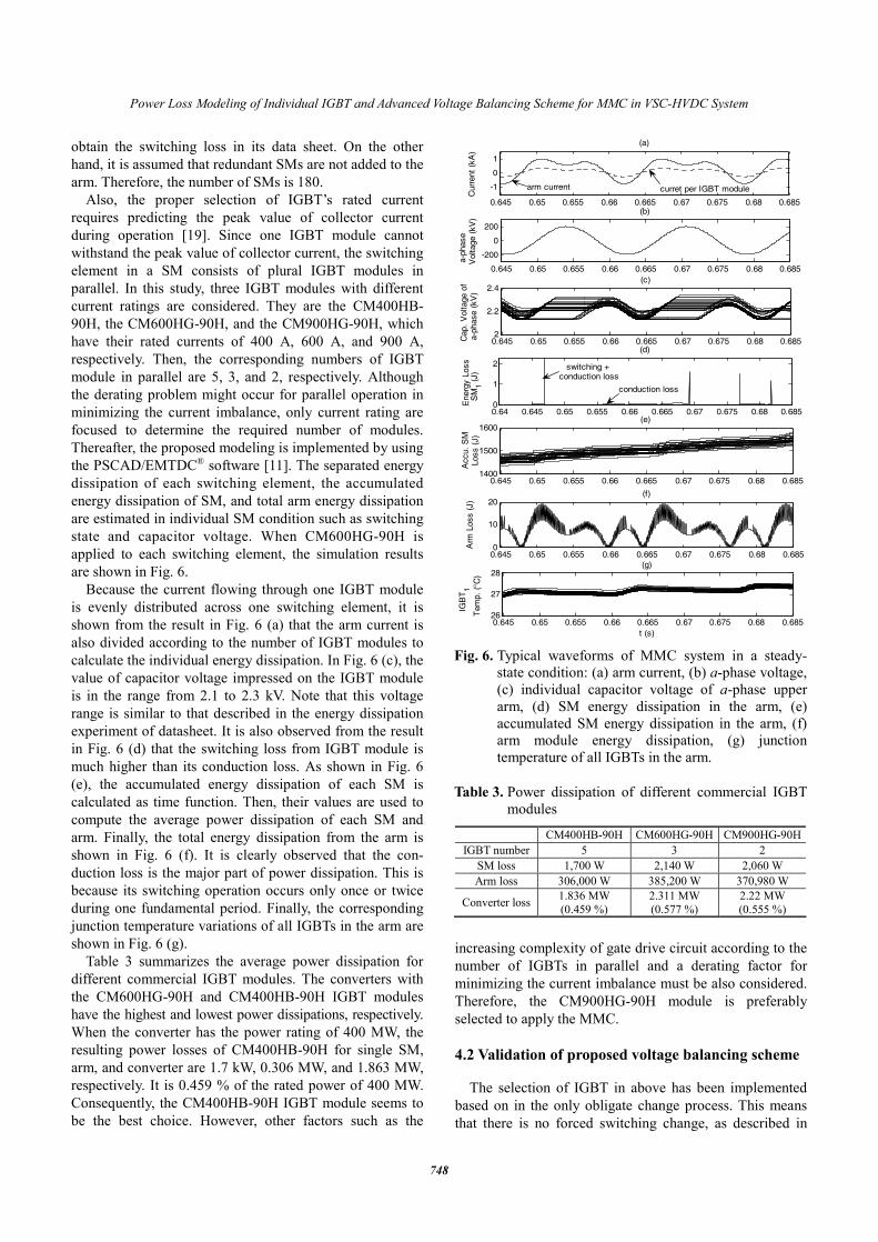
Also, the proper selection of IGBT’s rated current requires predicting the peak value of collector current during operation [19]. Since one IGBT module cannot withstand the peak value of collector current, the switching element in a SM consists of plural IGBT modules in parallel. In this study, three IGBT modules with different current ratings are considered. They are the CM400HB-90H, the CM600HG-90H, and the CM900HG-90H, which have their rated currents of 400 A, 600 A, and 900 A, respectively. Then, the corresponding numbers of IGBT module in parallel are 5, 3, and 2, respectively. Although the derating problem might occur for parallel operation in minimizing the current imbalance, only current rating are focused to determine the required number of modules. Thereafter, the proposed modeling is implemented by using the PSCAD/EMTDC® software [11]. The separated energy dissipation of each switching element, the accumulated energy dissipation of SM, and total arm energy dissipation are estimated in individual SM condition such as switching state and capacitor voltage. When CM600HG-90H is applied to each switching element, the simulation results are shown in Fig. 6.
Because the current flowing through one IGBT module is evenly distributed across one switching element, it is shown from the result in Fig. 6 (a) that the arm current is also divided according to the number of IGBT modules to calculate the individual energy dissipation. In Fig. 6 (c), the value of capacitor voltage impressed on the IGBT module is in the range from 2.1 to 2.3 kV. Note that this voltage range is similar to that described in the energy dissipation experiment of datasheet. It is also observed from the result in Fig. 6 (d) that the switching loss from IGBT module is much higher than its conduction loss. As shown in Fig. 6 (e), the accumulated energy dissipation of each SM is calculated as time function. Then, their values are used to compute the average power dissipation of each SM and arm. Finally, the total energy dissipation from the arm is shown in Fig. 6 (f). It is clearly observed that the con-duction loss is the major part of power dissipation. This is because its switching operation occurs only once or twice during one fundamental period. Finally, the corresponding junction temperature variations of all IGBTs in the arm are shown in Fig. 6 (g).
Table 3 summarizes the average power dissipation for different commercial IGBT modules. The converters with the CM600HG-90H and CM400HB-90H IGBT modules have the highest and lowest power dissipations, respectively. When the converter has the power rating of 400 MW, the resulting power losses of CM400HB-90H for single SM, arm, and converter are 1.7 kW, 0.306 MW, and 1.863 MW, respectively. It is 0.459 % of the rated power of 400 MW. Consequently, the CM400HB-90H IGBT module seems to be the best choice. However, other factors such as the
increasing complexity of gate drive circuit according to the number of IGBTs in parallel and a derating factor for minimizing the current imbalance must be also considered. Therefore, the CM900HG-90H module is preferably selected to apply the MMC.
4.2 Validation of proposed voltage balancing scheme
The selection of IGBT in above has been implemented
based on in the only obligate change process. This means that there is no forced switching change, as described in
0.645 0.65 0.655 0.66 0.665 0.67 0.675 0.68 0.685
-1
0
1
Cur
rent
(kA
)
(a)
0.645 0.65 0.655 0.66 0.665 0.67 0.675 0.68 0.685
-200
0
200
a-ph
ase
Vol
tage
(kV
)
(b)
0.645 0.65 0.655 0.66 0.665 0.67 0.675 0.68 0.6852
2.2
2.4
Cap
. Vol
tage
of
a-ph
ase
(kV
) (c)
0.64 0.645 0.65 0.655 0.66 0.665 0.67 0.675 0.68 0.6850
1
2
Ene
rgy
Loss
S
M1 (J
)
(d)
0.645 0.65 0.655 0.66 0.665 0.67 0.675 0.68 0.6851400
1500
1600
Acc
u. S
M
Loss
(J)
(e)
0.645 0.65 0.655 0.66 0.665 0.67 0.675 0.68 0.6850
10
20
Arm
Los
s (J
)
(f)
0.645 0.65 0.655 0.66 0.665 0.67 0.675 0.68 0.68526
27
28
IGB
T 1
Tem
p. (°
C)
t (s)
(g)
arm current curret per IGBT module
switching + conduction loss
conduction loss
Fig. 6. Typical waveforms of MMC system in a steady-
state condition: (a) arm current, (b) a-phase voltage, (c) individual capacitor voltage of a-phase upper arm, (d) SM energy dissipation in the arm, (e) accumulated SM energy dissipation in the arm, (f) arm module energy dissipation, (g) junction temperature of all IGBTs in the arm.
Table 3. Power dissipation of different commercial IGBT
modules
CM400HB-90H CM600HG-90H CM900HG-90H IGBT number 5 3 2
SM loss 1,700 W 2,140 W 2,060 W Arm loss 306,000 W 385,200 W 370,980 W
Converter loss 1.836 MW (0.459 %)
2.311 MW (0.577 %)
2.22 MW (0.555 %)

Gum Tae Son, Soo Hyoung Lee and Jung-Wook Park
749
Section 2.4. In order to improve the performance of MMC system, the proposed voltage balancing scheme is applied by the forced switching change. With the selected IGBT specification (CM900HG-90H) and the given capacitance (19 mF), the three different results, which are the SM state variations per 1 s, the peak-to-peak capacitor voltage ripple, and the individual SM loss, are shown in Figs. 7 (a), (b), and (c), respectively.
In the case of no forced change (k = 0), the state variation of each SM is 120 per 1 s. This means that there are only two state variations during one cycle of output voltage. The corresponding capacitor voltage ripple is in the range of 8.7 % at the rated voltage of 2.2 kV. And, the converter loss is 0.459 % at the rated power. When k = 1, the state variations increases to 360, and the converter loss increases to 0.9612 % at the rated power. However, the capacitor voltage ripple is reduced to the range of 7.13 %. Although there are some disadvantages for converter loss, the manufacturer might be able to reduce the capacitance within the given range of capacitor voltage ripple. Similarly, when the number of forced change keeps increasing, the converter loss is also increased exponentially. However, the capacitor voltage ripple is not reduced substantially. As the result, only one forced switching change provides the best performance when compared to the others.
In order to figure out the performance of advanced voltage balancing method, the dynamic waveform depend-ing on the forced change number is shown in Fig. 8 with the selected IGBT specification (CM900HG-90H) and the given capacitance (19 mF). Based on the grouping method, Figs. 8 (a) and (b) represents the output waveform when the forced change number is 0. On the other hand, the typical waveform using advanced voltage balancing method with 1 forced change number is shown in Fig. 8 (c) and (d). Comparing between Figs. 8 (b) and (d), the capacitor voltage ripple is dramatically reduced by applying the
proposed method. However, the loss is increased as the number of switching is increased from Fig. (a) and (c). Therefore, it is a tradeoff between power dissipation and capacitor rate decision.
4.3 Application to practical VSC-HVDC system
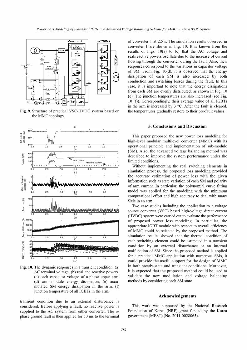
The proposed power loss modeling is applied to the
practical VSC-HVDC system in Fig. 9, as reported in the Trans Bay Cable Project [13]. It transfers the real power of 400 MW from converter 1 to converter 2 through the submarine XLPE DC cable with the length of 88 km. Its specification is equal to the typical MMC described in the previous subsection. A single arm has 180 SMs, and the voltage rating of DC bus is 400 kV. Then, the CM900HG-90H IGBT module is applied as a switching element.
To control the VSC-HVDC system in Fig. 9, the supervisory controller must generate the appropriate reference signals for both converters. Then, the vector-control scheme based on the synchronous reference frame is used to enable the independent control of active and reactive powers. In other words, the d-axis current regulates the real power and the DC bus voltage. The q-axis current deals with the reactive power. The control for inherent topological properties such as the elimination of circulating current is not considered in this study
As mentioned previously, the proposed power loss modeling can be applied to describe the energy dissipation of each SM in both transient and steady-state conditions. Note that the transient condition might be caused by the inner malfunction in SM and/or external disturbance. Then, by the power loss modeling from each switching element, it is possible to estimate its thermal state. In this study, the
0
500
1000
1500
2000
2500
Sta
te v
aria
tion
per
1 s
Number of forced switching change
(a)
0
1
2
3
4
5
6
7
8
9
Vol
tage
var
iatio
n w
ide
(%)
(b)
0
2000
4000
6000
8000
10000
12000
14000
Indi
viua
l SM
Los
s (J
)
(c)
0 1 2 10 0 1 2 10 0 1 2 10
Fig. 7. Comparison of performance corresponding to the forced switching change: (a) state variation per 1s, (b) voltage ripple band, (c) individual SM loss.
0.645 0.65 0.655 0.66 0.665 0.67 0.675 0.68 0.6850
50
Arm
Los
s (J
)
(a)
0.645 0.65 0.655 0.66 0.665 0.67 0.675 0.68 0.6852
2.2
2.4
Cap
. V
olta
ge o
f a-
phas
e (k
V)
(b)
0.645 0.65 0.655 0.66 0.665 0.67 0.675 0.68 0.6850
50
Arm
Los
s (J
)
(c)
0.645 0.65 0.655 0.66 0.665 0.67 0.675 0.68 0.6852
2.2
2.4
Cap
. V
olta
ge o
f a-
phas
e (k
V)
(d)
t(s) Fig. 8. Typical waveforms of advanced voltage balancing
method: (a) arm loss with 0 forced change, (b) individual capacitor voltage of a-phase upper arm with 0 forced change, (c) arm loss with 1 forced change, (d) individual capacitor voltage of a-phase upper arm with 1 forced change.
Power Loss Modeling of Individual IGBT and Advanced Voltage Balancing Scheme for MMC in VSC-HVDC System
750
transient condition due to an external disturbance is considered. Before applying a fault, no reactive power is supplied to the AC system from either converter. The a-phase ground fault is then applied for 50 ms to the terminal
of converter 1 at 2.5 s. The simulation results observed in converter 1 are shown in Fig. 10. It is known from the results of Figs. 10(a) to (c) that the AC voltage and real/reactive powers oscillate due to the increase of current flowing through the converter during the fault. Also, their responses correspond to the variations in capacitor voltage of SM. From Fig. 10(d), it is observed that the energy dissipation of each SM is also increased by both conduction and switching losses during the fault. In this case, it is important to note that the energy dissipations from each SM are evenly distributed, as shown in Fig. 10 (e). The junction temperatures are also increased (see Fig. 10 (f)). Correspondingly, their average value of all IGBTs in the arm is increased by 3 °C. After the fault is cleared, the temperatures gradually restore to their pre-fault values.
5. Conclusions and Discussion This paper proposed the new power loss modeling for
high-level modular multilevel converter (MMC) with its operational principle and implementation of sub-module (SM). Also, the advanced voltage balancing method was described to improve the system performance under the limited conditions.
Without implementing the real switching elements in simulation process, the proposed loss modeling provided the accurate estimation of power loss with the given information such as state variation of each SM and polarity of arm current. In particular, the polynomial curve fitting model was applied for the modeling with the minimum computational effort and high accuracy to deal with many SMs in an arm.
Two case studies including the application to a voltage source converter (VSC) based high-voltage direct current (HVDC) system were carried out to evaluate the performance of proposed power loss modeling. In particular, the appropriate IGBT module with respect to overall efficiency of MMC could be selected by the proposed method. The simulation results showed that the thermal condition of each switching element could be estimated in a transient condition by an external disturbance or an internal malfunction of SM. Since the proposed method is applied for a practical MMC application with numerous SMs, it could provide the useful support for the design of MMC in both steady-state and transient conditions. Moreover, it is expected that the proposed method could be used to validate the new modulation and voltage balancing methods by considering each SM state.
Acknowledgements This work was supported by the National Research
Foundation of Korea (NRF) grant funded by the Korea government (MEST) (No. 2011-0028065).
abciabcv
_DC recv_DC refv
recP
recQ
di qi dv qv
SMvarmi
armi
Fig. 9. Structure of practical VSC-HVDC system based on
the MMC topology.
2.4 2.5 2.6 2.7 2.8 2.9
0
200
400
600
Pow
er (M
W)
(b)2.4 2.5 2.6 2.7 2.8 2.9
140
160
180
AC
out
put
vo
ltage
(kV
)
(a)
2.4 2.5 2.6 2.7 2.8 2.9
2
2.5
3
Cap
. vol
tage
of
a-ph
ase
(kV
)
(c)
2.4 2.5 2.6 2.7 2.8 2.98000
9000
10000
11000
Acc
u. S
M L
oss
(J) (e)
2.4 2.5 2.6 2.7 2.8 2.90
50
100
Arm
Los
s (J
)
(d)
2.4 2.5 2.6 2.7 2.8 2.9323436384042
IGB
T 1 Tem
p. (°
C)
t (s)
(f)
real powerreactive power
Fig. 10. The dynamic responses in a transient condition: (a)
AC terminal voltage, (b) real and reactive powers, (c) each capacitor voltage of a-phase upper arm, (d) arm module energy dissipation, (e) accu-mulated SM energy dissipation in the arm, (f) junction temperature of all IGBTs in the arm.

Gum Tae Son, Soo Hyoung Lee and Jung-Wook Park
751
References
[1] J. Dorn, H. Huang, and D. Retzmann, “Novel voltage-sourced converters for HVDC and FACTS applications” in Proc. CIGRE Meeting, 2007, pp. 314-321.
[2] J. Dorn, H. Huang, and D. Retzmann, “A new multilevel voltage-sourced converter topology for HVDC application,” in Proc. CIGRE Meeting, 2008, Paris, pp. 1-8.
[3] M. Pereira, A. Zenkner and A. de Oliverira, “Full range active AC filter with mulitlevel IGBT con-verters for transmission and distribution systems,” in Proc. IEEE / PES Transmiss. Distrib. Conf. Expo., 2008, pp. 1-6.
[4] W. Li, L. Gregoire, and J. Belanger, “Control and performance of a modular multilevel converter system” in Proc. CIGRE Meeting, 2011, pp. 1-8.
[5] G. T. Son, H. –J. Lee, T. S. Nam, Y. –H. Chung, U. –H. Lee, S.–T. Baek, K. Hur, and Jung-Wook Park, “Design and control of a modular multilevel HVDC converter with redundant power modules for noninterruptible energy transfer,” IEEE Trans. Power Del., vol. 27, no. 3, pp. 1611-1619, July 2012.
[6] A. D. Rajapskse, A. M. Gole, and R. P. Jayasinghe, “An improved representation of FACTS controller semiconductor losses in EMTP-type programs using accurate loss-power injection into network solution,” IEEE Trans. Power Del., vol. 24, no. 1, pp. 381-389, Jan. 2009.
[7] U. N. Gnararatha, A. M. Gole, A. D. Rajapakse, and S. K. Chaudhary, “Loss estimation of modular multi-level converters using electro-magnetic transients simulation,” in Proc. Int. Conf. Power Syst. Transient (IPST), 2011.
[8] S. Allebrod, R. Hamerski, and R. Marquardt, “New transformerless, scalable modular multilevel con-verters for HVDC-transmission,” in Proc. Power Electron. Spec. (PESC) 2008 Conf., 2008, pp. 174-179.
[9] C. Wong, “EMTP modeling of IGBT dynamic performance for power dissipation estimation,” IEEE Trans. Ind. Appl., vol. 33, no. 1, Jan. 1997.
[10] U. N. Gnanarathna, A. M. Gole, and R. P. Jayasinghe, “Efficient modeling of modular multilevel HVDC converters (MMC) on elelctromagnetic transient simulation programs,” IEEE Trans. Power Del., vol. 26, no. 1, pp.316-324, Jan. 2011.
[11] User’s Guide: Comprehensive Resource for EMTDC-Transient Analysis for PSCAD Power System Simul-ation. Winnipeg, MB, Canada: Manitoba HVDC Res. Ctr., 2005.
[12] R. Marquardt, and A. Lesnicar, “A new modular voltage source inverter topology,” in Proc. Euro. Conf. Power Electron. Appl. (EPE), 2003, CD-ROM.
[13] S. P, Teeuwsen, “Modeling the trans-bay cable project as voltage-sourced converter with modular multilevel converter design,” in Proc. IEEE Power
Eng. Soc. Gen. Meeting (PES), 2011 pp. 1- 8. [14] U. Drofenik and J. W. Kolar, “Thermal analysis of a
multi-chip Si/SiC-power module for realization of a bridge leg of a 10kW vienna rectifier,” in Proc. 25th IEEE Int. Telecommuni. Energy Conf., 2003, pp. 826-833.
[15] A. M. Bazzi, P. T. Krein, J. W. Kimball, and K. Kepley, “IGBT and diode loss estimation under hysteresis switching,” IEEE Trans. Power Electron., vol. 27, No. 3, pp. 1044-1048, March 2012.
[16] A. D. Rajapskse, A. M. Gole, and P. L. Wilson, “Electromagnetic transient simulation models for accurate representation of switching losses and thermal performance in power electronic systems,” IEEE Trans. Power Del., vol. 20, no. 1, pp. 319-327, Jan. 2005.
[17] T. Bruckner, and S. Bernet, “Estimation and measurement of junction temperature in a three-level voltage source converter,” IEEE Trans. Power Electron., vol. 22, No. 1, pp. 3-12, Jan. 2007.
[18] N. Mohan, T. M. Undeland, and W. P. Robbins, Power Electronics Converters, Applications and Design, Media Enhanced Third Edition ed. New York: Wiley, 2003.
[19] Mitsubishi Electric IGBT Modules Application Note, pp.48-49, Dec. 2007. [Online]. Available: http://www. mitsubishielectric.com/semiconductors/products/powermod/note/
Gum Tae Son received the B.S and Ph.D. degrees from the School of Electrical and Electronic Engineering, Yonsei University, Seoul, Korea, in 2007 and 2013, respectively. He is cur-rently an Associate Research Engineer in the LS IS Co. Ltd, Anyang-si, Gyeonggi-do, Korea. His research
interests include flexible ac transmission system, CSC high-voltage direct current system, VSC high-voltage direct current system, wind-turbine generator system and modular multilevel system design.
Soo Hyoung Lee received the B.S. and Ph.D. degrees from the School of Electrical and Electronic Engineering, Yonsei University, Seoul, Korea, in 2008 and 2012, respectively. He is currently a Post-doctoral Research As-sociate in the School of Electrical and Computer Engineering, Georgia Institute
of Technology, Atlanta, GA, USA. His research interests are in load flow of power system, optimal operation of grid-connected distributed generation systems, anti-islanding and inverter control for distributed generation systems, and measurement based load modeling. He was

Power Loss Modeling of Individual IGBT and Advanced Voltage Balancing Scheme for MMC in VSC-HVDC System
752
the recipient of the Gold Prize Paper Award from the TMS Institute of Technology and Second Prize Paper Award from the Yonsei Electric Power Research Center.
Jung-Wook Park was born in Seoul, Korea. He received the B.S. degree (summa cum laude) from the Depart-ment of Electrical Engineering, Yonsei University, Seoul, Korea, in 1999, and the M.S.E.C.E. and Ph.D. degrees from the School of Electrical and Computer Engineering, Georgia Institute of
Technology, Atlanta, USA in 2000 and 2003, respectively. He was a Post-doctoral Research Associate in the Department of Electrical and Computer Engineering, University of Wisconsin, Madison, USA during 2003-2004, and a Senior Research Engineer with LG Electronics Inc., Korea during 2004-2005. He is currently an Associate Professor in the School of Electrical and Electronic Engineering, Yonsei University, Seoul, Korea. He is now leading the National Leading Research Laboratory (NLRL) designated by Korea government to the subject of integrated optimal operation for smart grid. He is also a chair of Yonsei Power and Renewable Energy FuturE technology Research Center (Yonsei-PREFER) in School of Electrical and Electronic Engineering, Yonsei University, Seoul, Korea. His current research interests are in power system dynamics, renewable energies based distributed generations, power control of electric vehicle, and optimization control algorithms. Prof. Park was the recipient of Second Prize Paper Award in 2003 from Industry Automation Control Committee, Prize Paper Award in 2008 from Energy Systems Committee of the IEEE Industry Applications Society (IAS), and Young Scientist Presidential Award in 2013 from the Korean Academy of Science and Technology (KAST) and the Ministry of Science, ICT, and Future Planning, Korea.
Related Documents