Power Injection System for Photovoltaic Plants based on a Multiconverter Topology with DC-Link Capacitor Voltage Balancing Víctor Miñambres-Marcos, Enrique Romero-Cadaval, María Isabel Milanés-Montero, Miguel Ángel Guerrero-Martínez, Fermín Barrero-González and Pedro González Castrillo Power Electrical and Electronic Systems research group, Department of Electrical, Electronics and Automatic Engineering, School of Industrial Engineering, University of Extremadura, Avda. Elvas s/n 06006 Badajoz. Tel: +34 924286787. Fax: +34 924289601 [email protected] , [email protected] , [email protected] , [email protected] , [email protected] , [email protected] Abstract-This paper presents the simulation of a new topology for the power injection system of a single-phase grid connected photovoltaic generation system that is based on the parallel association of two voltage source inverters: one is a 3 level neutral point clamped operated using a low switching frequency strategy and the other is a 2 level inverter which operates with a pulse width modulation based strategy. The aim of this topology is that multilevel inverter injects the power and the other inverter controls the current quality. The DC-link capacitor voltage balancing is solved by using the redundant states of the multilevel inverter. The proposal optimizes the system design, allowing high power injection, permitting reduction of system losses and an increase of the energy injected into the grid. I. INTRODUCTION The number of photovoltaic generation systems (PVGS) is increasing very fast in Spain, which is principally due to the daylight hours with an optimal irradiance and temperature and to the Spanish government subsidies. The energy produced by a PVGS must be injected into the electric grid, according to pre-established quality and reliability specifications, without affecting grid’s normal operation. This involves a low harmonic distortion and an accurate synchronization for the current injected. The PVGS contains a power injection system (PIS) that has the function of injecting the power produced by the photovoltaic cell groups, converting the energy from the original DC form to the final AC form with the desired electrical characteristics. The part of the PIS that carries out this conversion is the inverter [1][2]. Usually, Pulse Width Modulation (PWM) based inverters [1][3] or multilevel topology inverters are used [1][4]. In this paper a new topology for the PIS based on the parallel association of two voltage source inverters (VSI) is presented and analyzed by means of simulation. The first one is a single-phase 3 level neutral point clamped inverter (3-L NPC) operated using a low switching frequency quasi- square voltage waveform strategy with selective harmonic elimination (SHE) which is called quasi-square waveform multilevel inverter (QSWMI) [5][6]. The second one is a single-phase 2 level inverter operated with a PWM hysteresis band strategy which is called high-switching-frequency inverter (HSFI). The general purpose of the QSWMI is to inject the power generated by the PVGS; while the HSFI controls the quality of the current injected into the grid. The PIS proposed is capable to inject a high amount of power due to the use of a multilevel inverter but at the same time it presents the challenge of the DC-link capacitor voltage balancing. This issue is solved by the redundant state selection (RSS) of the 3-L NPC [6]-[9]. II. PIS DESCRIPTION The grid connected PVGS scheme analyzed is shown in Fig. 1. A direct connection to the inverters without a previous DC/DC converter has been chosen. The upper inverter in the figure is the QSWMI or inverter 1 and the lower inverter is the HSFI or inverter 2. Both inverters are connected to the grid by means of the inductances L 1 and L 2 respectively, which are divided into two to avoid short-circuits. A. QSWMI The objective of this inverter is to inject the energy from the PVGS into the grid. In order to achieve this, controlling the fundamental component of the inverter voltage is sufficient, under the assumption that the voltage does not present harmonics. The power generated by the PVGS P PV , with negligible inverter losses, is equal to the power injected into the electric grid P S : ,1 cos , PV S S S P P VI ϕ = = (1) where V S is the RMS supply voltage, I S,1 the RMS fundamental supply current component, and φ is the displacement angle between voltage and fundamental current component, which must be null for a maximum efficiency. 12 a s + 11 a s + 2a s + Fig. 1. Proposed system scheme. 1121 978-1-4244-7020-4/10/$26.00 '2010 IEEE 2010, 12th International Conference on Optimization of Electrical and Electronic Equipment, OPTIM 2010

Welcome message from author
This document is posted to help you gain knowledge. Please leave a comment to let me know what you think about it! Share it to your friends and learn new things together.
Transcript
Power Injection System for Photovoltaic Plants based on a Multiconverter Topology with
DC-Link Capacitor Voltage Balancing
Víctor Miñambres-Marcos, Enrique Romero-Cadaval, María Isabel Milanés-Montero, Miguel Ángel Guerrero-Martínez, Fermín Barrero-González and Pedro González Castrillo
Power Electrical and Electronic Systems research group, Department of Electrical, Electronics and Automatic Engineering, School of Industrial Engineering, University of Extremadura, Avda. Elvas s/n 06006 Badajoz. Tel: +34 924286787. Fax: +34 924289601
[email protected], [email protected], [email protected], [email protected], [email protected], [email protected]
Abstract-This paper presents the simulation of a new topology for the power injection system of a single-phase grid connected photovoltaic generation system that is based on the parallel association of two voltage source inverters: one is a 3 level neutral point clamped operated using a low switching frequency strategy and the other is a 2 level inverter which operates with a pulse width modulation based strategy. The aim of this topology is that multilevel inverter injects the power and the other inverter controls the current quality. The DC-link capacitor voltage balancing is solved by using the redundant states of the multilevel inverter. The proposal optimizes the system design, allowing high power injection, permitting reduction of system losses and an increase of the energy injected into the grid.
I. INTRODUCTION
The number of photovoltaic generation systems (PVGS) is increasing very fast in Spain, which is principally due to the daylight hours with an optimal irradiance and temperature and to the Spanish government subsidies.
The energy produced by a PVGS must be injected into the electric grid, according to pre-established quality and reliability specifications, without affecting grid’s normal operation. This involves a low harmonic distortion and an accurate synchronization for the current injected.
The PVGS contains a power injection system (PIS) that has the function of injecting the power produced by the photovoltaic cell groups, converting the energy from the original DC form to the final AC form with the desired electrical characteristics. The part of the PIS that carries out this conversion is the inverter [1][2]. Usually, Pulse Width Modulation (PWM) based inverters [1][3] or multilevel topology inverters are used [1][4].
In this paper a new topology for the PIS based on the parallel association of two voltage source inverters (VSI) is presented and analyzed by means of simulation. The first one is a single-phase 3 level neutral point clamped inverter (3-L NPC) operated using a low switching frequency quasi-square voltage waveform strategy with selective harmonic elimination (SHE) which is called quasi-square waveform multilevel inverter (QSWMI) [5][6]. The second one is a single-phase 2 level inverter operated with a PWM hysteresis band strategy which is called high-switching-frequency inverter (HSFI).
The general purpose of the QSWMI is to inject the power generated by the PVGS; while the HSFI controls the quality
of the current injected into the grid. The PIS proposed is capable to inject a high amount of power due to the use of a multilevel inverter but at the same time it presents the challenge of the DC-link capacitor voltage balancing. This issue is solved by the redundant state selection (RSS) of the 3-L NPC [6]-[9].
II. PIS DESCRIPTION
The grid connected PVGS scheme analyzed is shown in Fig. 1. A direct connection to the inverters without a previous DC/DC converter has been chosen. The upper inverter in the figure is the QSWMI or inverter 1 and the lower inverter is the HSFI or inverter 2. Both inverters are connected to the grid by means of the inductances L1 and L2 respectively, which are divided into two to avoid short-circuits.
A. QSWMI The objective of this inverter is to inject the energy from
the PVGS into the grid. In order to achieve this, controlling the fundamental component of the inverter voltage is sufficient, under the assumption that the voltage does not present harmonics. The power generated by the PVGS PPV, with negligible inverter losses, is equal to the power injected into the electric grid PS: ,1 cos ,PV S S SP P V I ϕ= = (1) where VS is the RMS supply voltage, IS,1 the RMS fundamental supply current component, and φ is the displacement angle between voltage and fundamental current component, which must be null for a maximum efficiency.
1 2as+
1 1as+
2as+
Fig. 1. Proposed system scheme.
1121978-1-4244-7020-4/10/$26.00 '2010 IEEE
2010, 12th International Conference on Optimization of Electrical and Electronic Equipment, OPTIM 2010
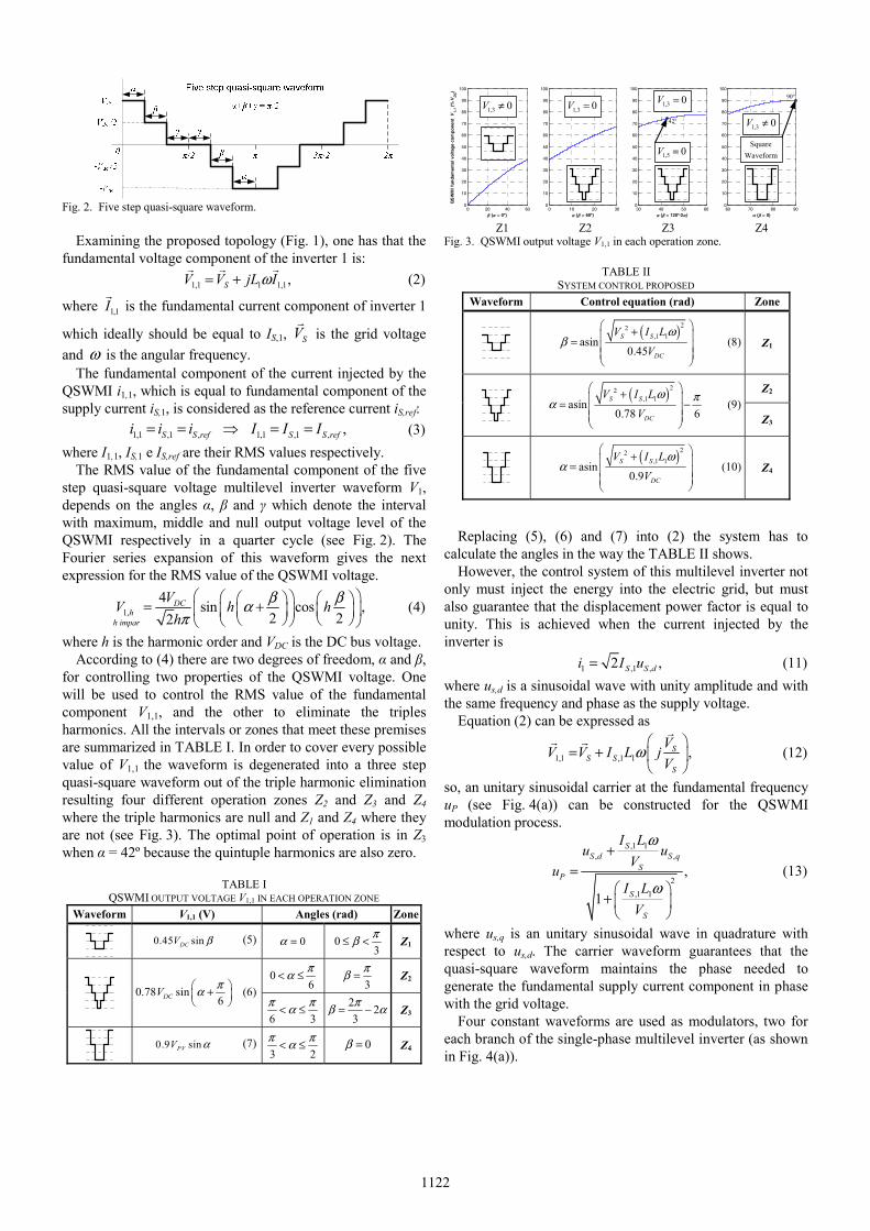
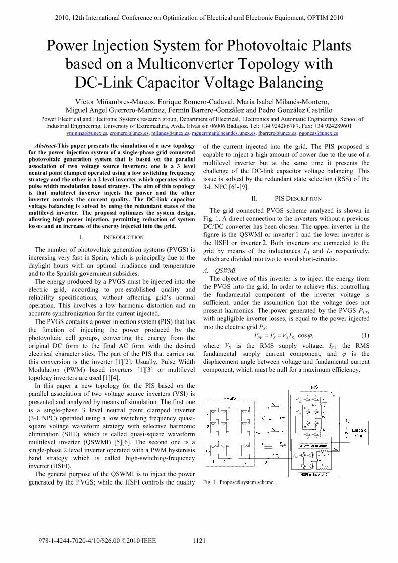
Fig. 2. Five step quasi-square waveform.
Examining the proposed topology (Fig. 1), one has that the
fundamental voltage component of the inverter 1 is: 1,1 1 1,1,SV V jL Iω= + (2)
where 1,1I is the fundamental current component of inverter 1
which ideally should be equal to IS,1, SV is the grid voltage and ω is the angular frequency.
The fundamental component of the current injected by the QSWMI i1,1, which is equal to fundamental component of the supply current iS,1, is considered as the reference current iS,ref: 1,1 ,1 , 1,1 ,1 , ,S S ref S S refi i i I I I= = ⇒ = = (3) where I1,1, IS,1 e IS,ref are their RMS values respectively.
The RMS value of the fundamental component of the five step quasi-square voltage multilevel inverter waveform V1, depends on the angles α, β and γ which denote the interval with maximum, middle and null output voltage level of the QSWMI respectively in a quarter cycle (see Fig. 2). The Fourier series expansion of this waveform gives the next expression for the RMS value of the QSWMI voltage.
1,4 sin cos ,
2 22DC
hh impar
VV h hh
β βαπ⎛ ⎞⎛ ⎞⎛ ⎞ ⎛ ⎞= +⎜ ⎟⎜ ⎟ ⎜ ⎟⎜ ⎟⎝ ⎠ ⎝ ⎠⎝ ⎠⎝ ⎠
(4)
where h is the harmonic order and VDC is the DC bus voltage. According to (4) there are two degrees of freedom, α and β,
for controlling two properties of the QSWMI voltage. One will be used to control the RMS value of the fundamental component V1,1, and the other to eliminate the triples harmonics. All the intervals or zones that meet these premises are summarized in TABLE I. In order to cover every possible value of V1,1 the waveform is degenerated into a three step quasi-square waveform out of the triple harmonic elimination resulting four different operation zones Z2 and Z3 and Z4 where the triple harmonics are null and Z1 and Z4 where they are not (see Fig. 3). The optimal point of operation is in Z3 when α = 42º because the quintuple harmonics are also zero.
TABLE I
QSWMI OUTPUT VOLTAGE V1,1 IN EACH OPERATION ZONE Waveform V1,1 (V) Angles (rad) Zone
0.45 sinDCV β (5) 0α = 0
3πβ≤ < Z1
0.78 sin
6DCV πα⎛ ⎞+⎜ ⎟⎝ ⎠
(6)0
6πα< ≤
3πβ = Z2
6 3π πα< ≤ 2 2
3πβ α= − Z3
0.9 sinPVV α (7)
3 2π πα< ≤ 0β = Z4
Z1 Z2 Z3 Z4 Fig. 3. QSWMI output voltage V1,1 in each operation zone.
TABLE II
SYSTEM CONTROL PROPOSED Waveform Control equation (rad) Zone
( )22,1 1asin
0.45S S
DC
V I L
V
ωβ
⎛ ⎞+⎜ ⎟= ⎜ ⎟⎜ ⎟⎝ ⎠
(8) Z1
( )22,1 1asin
0.78 6S S
DC
V I L
V
ω πα⎛ ⎞+⎜ ⎟= −⎜ ⎟⎜ ⎟⎝ ⎠
(9)Z2
Z3
( )22,1 1asin
0.9S S
DC
V I L
V
ωα
⎛ ⎞+⎜ ⎟= ⎜ ⎟⎟⎜ ⎠⎝
(10) Z4
Replacing (5), (6) and (7) into (2) the system has to calculate the angles in the way the TABLE II shows.
However, the control system of this multilevel inverter not only must inject the energy into the electric grid, but must also guarantee that the displacement power factor is equal to unity. This is achieved when the current injected by the inverter is 1 ,1 ,2 ,S S di I u= (11) where us,d is a sinusoidal wave with unity amplitude and with the same frequency and phase as the supply voltage.
Equation (2) can be expressed as
1,1 ,1 1 ,SS S
S
VV V I L jV
ω⎛ ⎞
= + ⎜ ⎟⎝ ⎠
(12)
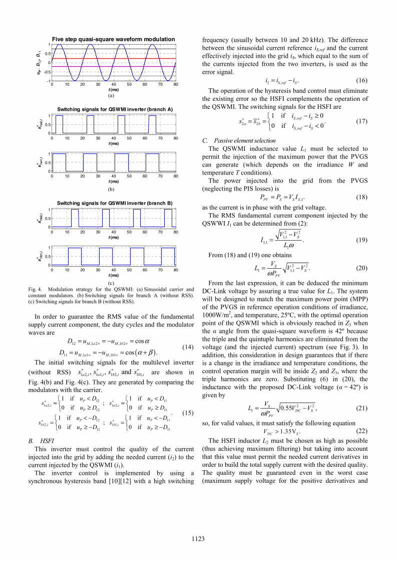
so, an unitary sinusoidal carrier at the fundamental frequency uP (see Fig. 4(a)) can be constructed for the QSWMI modulation process.
,1 1, ,
2,1 1
,
1
SS d S q
SP
S
S
I Lu u
VuI L
V
ω
ω
+=
⎛ ⎞+ ⎜ ⎟⎝ ⎠
(13)
where us,q is an unitary sinusoidal wave in quadrature with respect to us,d. The carrier waveform guarantees that the quasi-square waveform maintains the phase needed to generate the fundamental supply current component in phase with the grid voltage.
Four constant waveforms are used as modulators, two for each branch of the single-phase multilevel inverter (as shown in Fig. 4(a)).
0 20 40 600
10
20
30
40
50
60
70
80
90
100
QS
WM
I fu
nda
men
tal v
olta
ge
com
pone
ntV
1,1
(%
VD
C)
β (α = 0º)0 10 20 30
0
10
20
30
40
50
60
70
80
90
100
α (β = 60º)30 40 50 60
0
10
20
30
40
50
60
70
80
90
100
α (β = 120º-2α)60 70 80 90
0
10
20
30
40
50
60
70
80
90
100
α (β = 0)
1,3 0V ≠ 1,3 0V = 1,3 0V =
1,5 0V =
1,3 0V ≠
SquareWaveform
42º
90º
1122
(a)
(b)
(c)
Fig. 4. Modulation strategy for the QSWMI: (a) Sinusoidal carrier and constant modulators. (b) Switching signals for branch A (without RSS). (c) Switching signals for branch B (without RSS).
In order to guarantee the RMS value of the fundamental
supply current component, the duty cycles and the modulator waves are
( )
12 ,1 2 ,1 2
11 ,1 1 ,1 1
cos
cos .M a M b
M a M b
D u u
D u u
αα β
+ +
+ +
= = − =
= = − = + (14)
The initial switching signals for the multilevel inverter (without RSS) 1 2, 1 1, 1 2, 1 1,, , and a i a i b i b is s s s+ + + + are shown in Fig. 4(b) and Fig. 4(c). They are generated by comparing the modulators with the carrier.
12 111 2, 1 2,
12 11
12 111 2, 1 1,
12 11
1 if 1 if ;
0 if 0 if .
1 if 1 if ;
0 if 0 if
P Pa i a i
P P
P Pb i b i
P P
u D u Ds s
u D u D
u D u Ds s
u D u D
+ +
+ +
< <⎧ ⎧= =⎨ ⎨≥ ≥⎩ ⎩
< − < −⎧ ⎧= =⎨ ⎨≥ − ≥ −⎩ ⎩
(15)
B. HSFI This inverter must control the quality of the current
injected into the grid by adding the needed current (i2) to the current injected by the QSWMI (i1).
The inverter control is implemented by using a synchronous hysteresis band [10][12] with a high switching
frequency (usually between 10 and 20 kHz). The difference between the sinusoidal current reference iS,ref and the current effectively injected into the grid iS, which equal to the sum of the currents injected from the two inverters, is used as the error signal. 2 , .S ref Si i i= − (16)
The operation of the hysteresis band control must eliminate the existing error so the HSFI complements the operation of the QSWMI. The switching signals for the HSFI are
,2 2
,
1 if 0.
0 if 0S ref S
a bS ref S
i is s
i i+ + − ≥⎧
= = ⎨ − <⎩ (17)
C. Passive element selection The QSWMI inductance value L1 must be selected to
permit the injection of the maximum power that the PVGS can generate (which depends on the irradiance W and temperature T conditions).
The power injected into the grid from the PVGS (neglecting the PIS losses) is ,1.PV S S SP P V I= = (18) as the current is in phase with the grid voltage.
The RMS fundamental current component injected by the QSWWI I1 can be determined from (2):
2 2
1,11,1
1
.SV VI
L ω−
= (19)
From (18) and (19) one obtains
2 21 1,1 .S
SPV
VL V VPω
= − (20)
From the last expression, it can be deduced the minimum DC-Link voltage by assuring a true value for L1. The system will be designed to match the maximum power point (MPP) of the PVGS in reference operation conditions of irradiance, 1000W/m2, and temperature, 25ºC, with the optimal operation point of the QSWMI which is obviously reached in Z3 when the α angle from the quasi-square waveform is 42º because the triple and the quintuple harmonics are eliminated from the voltage (and the injected current) spectrum (see Fig. 3). In addition, this consideration in design guarantees that if there is a change in the irradiance and temperature conditions, the control operation margin will be inside Z2 and Z3, where the triple harmonics are zero. Substituting (6) in (20), the inductance with the proposed DC-Link voltage (α = 42º) is given by
2 21 0.55 ,S
DC SPV
VL V VPω
= − (21)
so, for valid values, it must satisfy the following equation 1.35V .DC SV > (22)
The HSFI inductor L2 must be chosen as high as possible (thus achieving maximum filtering) but taking into account that this value must permit the needed current derivatives in order to build the total supply current with the desired quality. The quality must be guaranteed even in the worst case (maximum supply voltage for the positive derivatives and
0 10 20 30 40 50 60 70 80-1
-0.5
0
0.5
1Five step quasi-square waveform modulation
u P ,
D1
2, D
11
t (ms)
0 10 20 30 40 50 60 70 800
0.5
1
Switching signals for QSWMI inverter (branch A)
s 1a2
,i+
t (ms)
0 10 20 30 40 50 60 70 800
0.5
1
s 1a
1,i
+
t (ms)
0 10 20 30 40 50 60 70 800
0.5
1
Switching signals for QSWMI inverter (branch B)
s 1b
2,i
+
t (ms)
0 10 20 30 40 50 60 70 800
0.5
1
s 1b
1,i
+
t (ms)
1123
minimum for the negative ones). For a given current derivative or slope, i2,slope, one has
22,
2 .DC S
slope
V VLi−= (23)
To produce valid inductance values, one must have that 1.41V .DC SV > (24) This condition is more restrictive for the DC-Link voltage than the one imposed by (22).
The capacitors between the PVGS and the PIS C1 and C2 (that ideally have the same value and are equal to C/2) must absorb the active power fluctuations (that always exist in a single-phase system). Therefore it achieves constant power extracted from the PVGS, by keeping the DC voltage at the output terminal of the PVGS constant under these power fluctuations.
As the supply current is in phase with the grid voltage, and assuming it to be sinusoidal, the instantaneous power becomes 2( ) ( ) ( ) 2 sinS S S S Sp t v t i t V I tω= = (25) and the power fluctuations are due to the energy that is stored and discharged in the capacitor, so that the instantaneous power associated with the capacitor is
2
( ) ( ) ( )
2 sin ( cos2 ).C S PV S S
S S S S S S
p t p t P p t P
V I t V I V I tω ω= − = − =
= − = − (26)
The energy discharged from the capacitor in one quarter of the fundamental period (which will be equal to the energy stored in the next quarter) is
( )( )
( )
3 38 8
8 8
8
38
( ) ( ) cos 2
1 sin 2 .2
T T
C C S ST T
T
S S PVS S
T
e t p t dt V I t dt
V I PV I t
ω
ωω ω ω
= = − =
⎡ ⎤⎢ ⎥= = =⎢ ⎥⎢ ⎥⎣ ⎦
∫ ∫
(27)
This discharged energy produces a capacitor voltage decrease:
( )2 2,max ,min
1( )2C C Ce t C V V= − (28)
If the voltage decrease is small, the above equation can be written as
( ) ( )( )2 21( ) 22C DC C DC C DC Ce t C V v V v CV v= + − − = (29)
where Cv is the capacitor voltage fluctuation.
To guarantee that the relative voltage fluctuations are lower than a pre-established value, they must satisfy
1 22 2 2
( ) 2 22 2 2
C C PV PV
DC DC DC DC
v e t P PC C CV CV C V V
εω εω
= = ≤ ⇒ = = ≥ (30)
where ε is the maximum relative value of the DC voltage ripple.
III. CAPACITORS VOLTAGE BALANCING
The capacitors voltage balancing is a problem inherent to
the multilevel inverter due to the asymmetric DC-Link current flow. Obviously, it must be solved to assure that the voltage levels of the DC-Link are the desired ones. In this case, it is needed a half of the DC-Link voltage in the middle point of the DC-Link so C1 must be equal to C2. The best way to solve this is to take advantage of the redundant states selection RSS of the 3L-NPC which permit the same output voltages for the inverter but with a different current flow. Looking at the proposed system scheme in Fig. 1, one can deduce that
22
22 1
01
1
PV DCC
PV C CPV DC
C
i iv
j Cv v v
i iv
j C
ω
ω
−⎧ =⎪⎪= + ⎨ +⎪ =⎪⎩
(31)
where vC2 and vC1 are the voltage at the capacitors C2 and C1 respectively, vPV and iPV are the PVGS voltage and current respectively, and iDC2 and iDC0 are the upper and lower DC-Link currents respectively.
To control the capacitors voltage balancing, vC2 must be equal to vC1. On the one side, from (31) one has that the DC-Link currents affect directly to the capacitors voltage, and from the other side one has the redundant states of the QSWMI which affects the DC-Link currents, so the control can be done by sensing the capacitors voltages and the load current and then selecting the switching state, SS, that balance the capacitors.
In the TABLE III are shown every SS of the full bridge QSWMI and its effect on the DC-Link capacitors voltages. In order to this, the control logic can be done with the redundant states: S1, S3, S5 and S7.The TABLE IV shows the selected switching state, SSS, according to the control logic
Once the SSS are calculated, it is compared with the initial switching state obtained in the QSWMI modulation process SSI and results the final switching state, SSF, (with the switching signals 1 2 1 1 1 2 1 1, , ,a a b bs s s s+ + + + ) that must be applied to the inverter.
IV. CONTROL SYSTEM
The PIS control can be divided into the blocks shown in the schematic diagram of Fig. 5.
TABLE III
SWITCHING STATES, OUTPUT VOLTAGES AND THEIR EFFECT ON THE DC-LINK CAPACITORS VOLTAGES
+1 2as +
1 1as +1 2bs +
1 1bs V1 Effect on C1 Effect on C2
SS> 0Si < 0Si > 0Si < 0Si
0 0 0 0 0 n/a n/a n/a n/a S0 0 0 0 1 -VDC/2 + - - + S1 0 0 1 1 -VDC n/a n/a n/a n/a S2 0 1 0 0 VDC/2 - + + - S3 0 1 0 1 0 n/a n/a n/a n/a S4 0 1 1 1 -VDC/2 - + + - S5 1 1 0 0 VDC n/a n/a n/a n/a S6 1 1 0 1 VDC/2 + - - + S7 1 1 1 1 0 n/a n/a n/a n/a S8
Here, “+”, “-” and “n/a” represent charging, discharging and no effect respectively.
1124
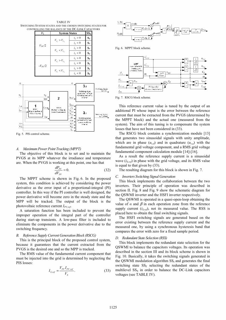
TABLE IV SWITCHING SYSTEM STATES AND THE CHOSEN SWITCHING STATES FOR
CONTROLLING THE BALANCE OF THE DC-LINK CAPACITORS V1 System States SSS
VDC/2 1 2C CV V>
0Si > S3 0Si < S7
1 2C CV V< 0Si > S7 0Si < S3
-VDC/2 1 2C CV V>
0Si > S5 0Si < S1
1 2C CV V< 0Si > S1 0Si < S5
ω
,S du,S qu
Fig. 5. PIS control scheme.
A. Maximum Power Point Tracking (MPPT) The objective of this block is to set and to maintain the
PVGS at its MPP whatever the irradiance and temperature are. When the PVGS is working at this point, one has that
0.PV
PV
dPdV
= (32)
The MPPT scheme is shown in Fig. 6. In the proposed system, this condition is achieved by considering the power derivative as the error input of a proportional-integral (PI) controller. In this way if the PI controller is well designed, the power derivative will become zero in the steady state and the MPP will be tracked. The output of the block is the photovoltaic reference current IPV,ref.
A saturation function has been included to prevent the improper operation of the integral part of the controller during start-up transients. A low-pass filter is included to eliminate the components in the power derivative due to the switching frequency.
B. Reference Supply Current Generation Block (RSCG) This is the principal block of the proposed control system,
because it guarantees that the current extracted from the PVGS is the desired one and so the MPP is tracked.
The RMS value of the fundamental current component that must be injected into the grid is determined by neglecting the PIS losses:
,, .PV PV ref
S refS
V II
V= (33)
Fig. 6. MPPT block scheme.
12
12
1ωω
,S du
,S qu,1,S qv+
,1,S dv+
Fig. 7. RSCG block scheme.
This reference current value is tuned by the output of an
additional PI whose input is the error between the reference current that must be extracted from the PVGS (determined by the MPPT block) and the actual one (measured from the system). The aim of this tuning is to compensate the system losses that have not been considered in (33).
The RSCG block contains a synchronization module [13] that generates two sinusoidal signals with unity amplitude, which are in phase (us,d) and in quadrature (us,q) with the fundamental grid voltage component, and a RMS grid voltage fundamental component calculation module [14]-[16].
As a result the reference supply current is a sinusoidal wave (iS,ref) in phase with the grid voltage, and its RMS value is equal to that given by (33).
The resulting diagram for this block is shown in Fig. 7.
C. Inverters Switching Signal Generation This block implements the collaboration between the two
inverters. Their principle of operation was described in section II. Fig. 8 and Fig. 9 show the schematic diagram for the QSWMI inverter and the HSFI inverter respectively.
The QSWMI is operated in a quasi-open-loop obtaining the value of α and β in each operation zone from the reference supply current (iS,ref), not its measured value. The RSS is placed here to obtain the final switching signals.
The HSFI switching signals are generated based on the error existing between the reference supply current and the measured one, by using a synchronous hysteresis band that compares the error with zero for a fixed sample period.
D. Redundant State Selection (RSS) This block implements the redundant state selection for the
QSWMI to balance the capacitors voltages. Its operation was described in the section III and its block scheme is shown in Fig. 10. Basically, it takes the switching signals generated in the QSWMI modulation algorithm SSI and generates the final switching state SSF selecting the redundant states of the multilevel SSS in order to balance the DC-Link capacitors voltages (see TABLE IV).
1125
6π>=
( )cos ββ
α
α
( )cos α
( )cos α
2 3π
( )cos α
( )cos α β+α β+
( )cos α β+α β+
3π>=
, 1S ref
S
I LV
ω
3π
0>=
Fig. 8. Switching signal generation for QSWMI with RSS.
Fig. 9. Switching signal generation for HSFI.
0==
Fig. 10. Redundant State Selection RSS.
The final switching signals are obtained with a look up
table LUT addressed by SSF. The final switching state selector also calculate the best zero output voltage state for the QSWMI (S0, S4 or S8) by choosing the redundant state that is adjacent to the previous state and the next one to guarantee the minimum simultaneous switching in the semiconductors. Looking at the modulation process, one can notice that the unique state that meets this objective is S4.
There are two operation modes for the redundant state control which are implemented at the end of the block diagram. The first one proposes a low switching frequency strategy for the RSS. This means that the RSS is only applied when the modulation of the QSWMI changes its state. The second one proposes a high switching frequency strategy for the RSS, that is, the RSS is applied when it can be applied so during the same QSWMI output voltage with redundant capability, the RSS changes the switching signals. The former has less stress for the semiconductors and less switching losses, but the latter improves the capacitors voltages balancing although it operates through non-adjacent states.
V. PIS EVALUATION THROUGH SIMULATION
The control system evaluation is described out in this section using the model in Fig. 11, showing how the PIS is able to set and maintain the PVGS at its MPP even when changing the operation irradiance or temperature.
Fig. 11. Simulated System scheme.
A model for the PVGS that permits on-line irradiance and
temperature changes is used [17]. The model of the DC-Link capacitors has been obtained following (31). The principal characteristics of the PVGS are summarized in TABLE V.
The simulated PVGS used for PIS evaluation has 16 series connected photovoltaic cells (Shell SP150-P). It produces a maximum power point voltage of about 550V for the reference operation conditions of irradiance, 1000W/m2, and temperature, 25ºC, that satisfies the condition imposed in (24)
The irradiance profile selected to evaluate the PIS are shown in Fig. 12. This profile simulates the decreasing irradiance level when the sun is shadowed by a cloud. The irradiance changes presented in this profile are sharper than usual, so the PIS is evaluated in a harsher than normal conditions.
The PIS parameters values used in the simulation test and the grid voltage are shown in TABLE VI. Note the deviation of 10% that has been applied to C1 for evaluating the system performance in these conditions.
TABLE V PVGS CHARACTERISTICS
Parameter Value Number of series-parallel connected cells 16-1 Photovoltaic cell reference SHELL SP150-P Short-circuit current (25ºC, 1000 W/m2) 4.8A Open-circuit voltage (25ºC, 1000 W/m2) 43.4V MPP current (25ºC, 1000 W/m2) 4.4A MPP voltage (25ºC, 1000 W/m2) 34V
1126
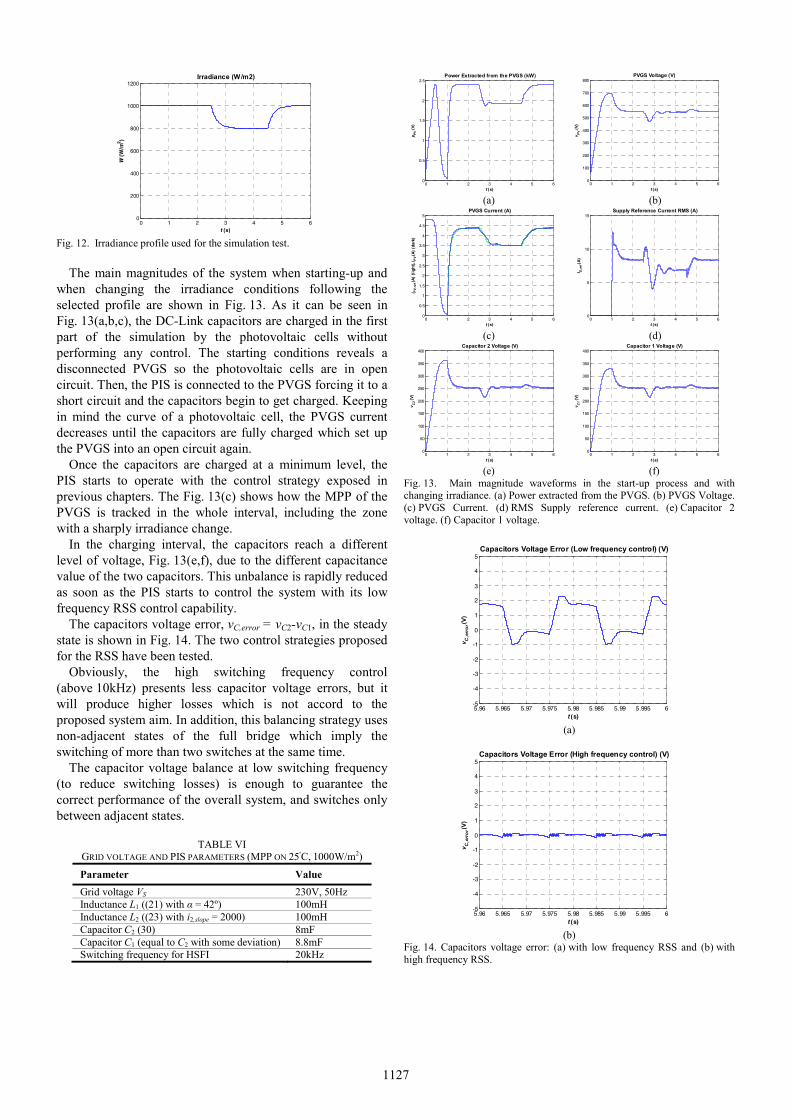
Fig. 12. Irradiance profile used for the simulation test.
The main magnitudes of the system when starting-up and
when changing the irradiance conditions following the selected profile are shown in Fig. 13. As it can be seen in Fig. 13(a,b,c), the DC-Link capacitors are charged in the first part of the simulation by the photovoltaic cells without performing any control. The starting conditions reveals a disconnected PVGS so the photovoltaic cells are in open circuit. Then, the PIS is connected to the PVGS forcing it to a short circuit and the capacitors begin to get charged. Keeping in mind the curve of a photovoltaic cell, the PVGS current decreases until the capacitors are fully charged which set up the PVGS into an open circuit again.
Once the capacitors are charged at a minimum level, the PIS starts to operate with the control strategy exposed in previous chapters. The Fig. 13(c) shows how the MPP of the PVGS is tracked in the whole interval, including the zone with a sharply irradiance change.
In the charging interval, the capacitors reach a different level of voltage, Fig. 13(e,f), due to the different capacitance value of the two capacitors. This unbalance is rapidly reduced as soon as the PIS starts to control the system with its low frequency RSS control capability.
The capacitors voltage error, vC,error = vC2-vC1, in the steady state is shown in Fig. 14. The two control strategies proposed for the RSS have been tested.
Obviously, the high switching frequency control (above 10kHz) presents less capacitor voltage errors, but it will produce higher losses which is not accord to the proposed system aim. In addition, this balancing strategy uses non-adjacent states of the full bridge which imply the switching of more than two switches at the same time.
The capacitor voltage balance at low switching frequency (to reduce switching losses) is enough to guarantee the correct performance of the overall system, and switches only between adjacent states.
TABLE VI
GRID VOLTAGE AND PIS PARAMETERS (MPP ON 25ºC, 1000W/m2)
Parameter Value Grid voltage VS 230V, 50Hz Inductance L1 ((21) with α = 42º) 100mH Inductance L2 ((23) with i2,slope = 2000) 100mH Capacitor C2 (30) 8mF Capacitor C1 (equal to C2 with some deviation) 8.8mF Switching frequency for HSFI 20kHz
(a) (b)
(c) (d)
(e) (f) Fig. 13. Main magnitude waveforms in the start-up process and with changing irradiance. (a) Power extracted from the PVGS. (b) PVGS Voltage. (c) PVGS Current. (d) RMS Supply reference current. (e) Capacitor 2 voltage. (f) Capacitor 1 voltage.
(a)
(b)
Fig. 14. Capacitors voltage error: (a) with low frequency RSS and (b) with high frequency RSS.
0 1 2 3 4 5 60
200
400
600
800
1000
1200Irradiance (W/m2)
W (
W/m
2 )
t (s)
0 1 2 3 4 5 60
0.5
1
1.5
2
2.5Power Extracted from the PVGS (kW)
t (s)
p PV (V
)
0 1 2 3 4 5 60
100
200
300
400
500
600
700
800PVGS Voltage (V)
t (s)
v PV (V
)
0 1 2 3 4 5 60
0.5
1
1.5
2
2.5
3
3.5
4
4.5
5PVGS Current (A)
i PV
,re
f (A
) (l
ight
), i P
V (A
) (d
ark)
t (s)0 1 2 3 4 5 6
0
5
10
15Supply Reference Current RMS (A)
I S,r
ef (
A)
t (s)
0 1 2 3 4 5 60
50
100
150
200
250
300
350
400Capacitor 2 Voltage (V)
t (s)
v C2 (V
)
0 1 2 3 4 5 60
50
100
150
200
250
300
350
400Capacitor 1 Voltage (V)
t (s)
v C1 (V
)
5.96 5.965 5.97 5.975 5.98 5.985 5.99 5.995 6-5
-4
-3
-2
-1
0
1
2
3
4
5Capacitors Voltage Error (Low frequency control) (V)
t (s)
v C,e
rror
(V)
5.96 5.965 5.97 5.975 5.98 5.985 5.99 5.995 6-5
-4
-3
-2
-1
0
1
2
3
4
5Capacitors Voltage Error (High frequency control) (V)
t (s)
v C,e
rror
(V)
1127
VI. PIS OPERATION ANALYSIS
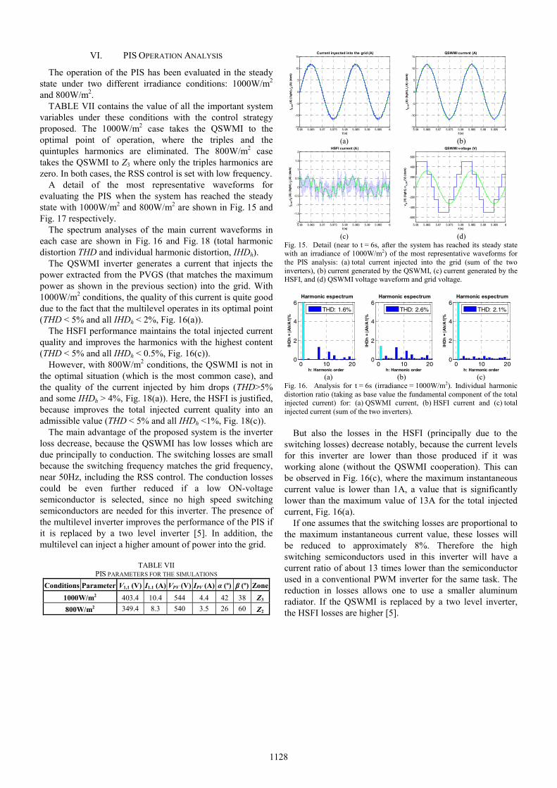
The operation of the PIS has been evaluated in the steady state under two different irradiance conditions: 1000W/m2 and 800W/m2.
TABLE VII contains the value of all the important system variables under these conditions with the control strategy proposed. The 1000W/m2 case takes the QSWMI to the optimal point of operation, where the triples and the quintuples harmonics are eliminated. The 800W/m2 case takes the QSWMI to Z3 where only the triples harmonics are zero. In both cases, the RSS control is set with low frequency.
A detail of the most representative waveforms for evaluating the PIS when the system has reached the steady state with 1000W/m2 and 800W/m2 are shown in Fig. 15 and Fig. 17 respectively.
The spectrum analyses of the main current waveforms in each case are shown in Fig. 16 and Fig. 18 (total harmonic distortion THD and individual harmonic distortion, IHDh).
The QSWMI inverter generates a current that injects the power extracted from the PVGS (that matches the maximum power as shown in the previous section) into the grid. With 1000W/m2 conditions, the quality of this current is quite good due to the fact that the multilevel operates in its optimal point (THD < 5% and all IHDh < 2%, Fig. 16(a)).
The HSFI performance maintains the total injected current quality and improves the harmonics with the highest content (THD < 5% and all IHDh < 0.5%, Fig. 16(c)).
However, with 800W/m2 conditions, the QSWMI is not in the optimal situation (which is the most common case), and the quality of the current injected by him drops (THD>5% and some IHDh > 4%, Fig. 18(a)). Here, the HSFI is justified, because improves the total injected current quality into an admissible value (THD < 5% and all IHDh <1%, Fig. 18(c)).
The main advantage of the proposed system is the inverter loss decrease, because the QSWMI has low losses which are due principally to conduction. The switching losses are small because the switching frequency matches the grid frequency, near 50Hz, including the RSS control. The conduction losses could be even further reduced if a low ON-voltage semiconductor is selected, since no high speed switching semiconductors are needed for this inverter. The presence of the multilevel inverter improves the performance of the PIS if it is replaced by a two level inverter [5]. In addition, the multilevel can inject a higher amount of power into the grid.
TABLE VII
PIS PARAMETERS FOR THE SIMULATIONS Conditions Parameter V1,1 (V) I1.1 (A) VPV (V) IPV (A) α (º) β (º) Zone
1000W/m2 403.4 10.4 544 4.4 42 38 Z3 800W/m2 349.4 8.3 540 3.5 26 60 Z2
(a) (b)
(c) (d) Fig. 15. Detail (near to t = 6s, after the system has reached its steady state with an irradiance of 1000W/m2) of the most representative waveforms for the PIS analysis: (a) total current injected into the grid (sum of the two inverters), (b) current generated by the QSWMI, (c) current generated by the HSFI, and (d) QSWMI voltage waveform and grid voltage.
(a) (b) (c) Fig. 16. Analysis for t = 6s (irradiance = 1000W/m2). Individual harmonic distortion ratio (taking as base value the fundamental component of the total injected current) for: (a) QSWMI current, (b) HSFI current and (c) total injected current (sum of the two inverters).
But also the losses in the HSFI (principally due to the
switching losses) decrease notably, because the current levels for this inverter are lower than those produced if it was working alone (without the QSWMI cooperation). This can be observed in Fig. 16(c), where the maximum instantaneous current value is lower than 1A, a value that is significantly lower than the maximum value of 13A for the total injected current, Fig. 16(a).
If one assumes that the switching losses are proportional to the maximum instantaneous current value, these losses will be reduced to approximately 8%. Therefore the high switching semiconductors used in this inverter will have a current ratio of about 13 times lower than the semiconductor used in a conventional PWM inverter for the same task. The reduction in losses allows one to use a smaller aluminum radiator. If the QSWMI is replaced by a two level inverter, the HSFI losses are higher [5].
5.96 5.965 5.97 5.975 5.98 5.985 5.99 5.995 6-15
-10
-5
0
5
10
15Current inyected into the grid (A)
i S,r
ef (
A)
(lig
ht),
i S (A
) (d
ark)
t (s)5.96 5.965 5.97 5.975 5.98 5.985 5.99 5.995 6
-15
-10
-5
0
5
10
15QSWMI current (A)
i S,r
ef (
A)
(lig
ht)
, i 1
(A)
(dar
k)
t (s)
5.96 5.965 5.97 5.975 5.98 5.985 5.99 5.995 6-2
-1.5
-1
-0.5
0
0.5
1
1.5
2HSFI current (A)
i S,r
ef-i
S (A
) (l
igh
t),
i 2 (A
) (d
ark)
t (s)5.96 5.965 5.97 5.975 5.98 5.985 5.99 5.995 6
-600
-400
-200
0
200
400
600
QSWMI voltage (V)
v S (
V) (
ligh
t),
v 1,L
N (
V) (
dark
)
t (s)
0 10 200
2
4
6Harmonic espectrum
h: Harmonic order
IHDh
= |A
h/A
1|%
THD: 1.6%
0 10 200
2
4
6Harmonic espectrum
h: Harmonic orderIH
Dh =
|Ah/
A1|
%
THD: 2.6%
0 10 200
2
4
6Harmonic espectrum
h: Harmonic order
IHDh
= |A
h/A
1|%
THD: 2.1%
1128
(a) (b)
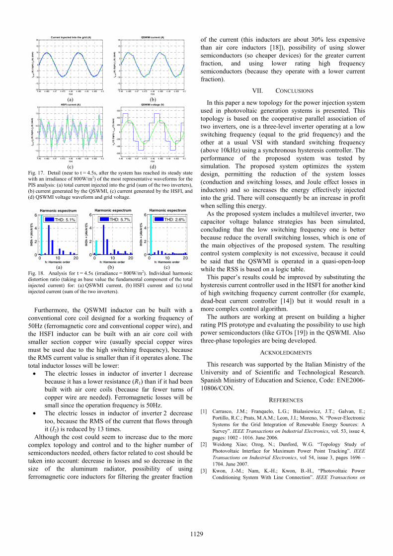
(c) (d) Fig. 17. Detail (near to t = 4.5s, after the system has reached its steady state with an irradiance of 800W/m2) of the most representative waveforms for the PIS analysis: (a) total current injected into the grid (sum of the two inverters), (b) current generated by the QSWMI, (c) current generated by the HSFI, and (d) QSWMI voltage waveform and grid voltage.
(a) (b) (c) Fig. 18. Analysis for t = 4.5s (irradiance = 800W/m2). Individual harmonic distortion ratio (taking as base value the fundamental component of the total injected current) for: (a) QSWMI current, (b) HSFI current and (c) total injected current (sum of the two inverters).
Furthermore, the QSWMI inductor can be built with a
conventional core coil designed for a working frequency of 50Hz (ferromagnetic core and conventional copper wire), and the HSFI inductor can be built with an air core coil with smaller section copper wire (usually special copper wires must be used due to the high switching frequency), because the RMS current value is smaller than if it operates alone. The total inductor losses will be lower:
• The electric losses in inductor of inverter 1 decrease because it has a lower resistance (R1) than if it had been built with air core coils (because far fewer turns of copper wire are needed). Ferromagnetic losses will be small since the operation frequency is 50Hz.
• The electric losses in inductor of inverter 2 decrease too, because the RMS of the current that flows through it (I2) is reduced by 13 times.
Although the cost could seem to increase due to the more complex topology and control and to the higher number of semiconductors needed, others factor related to cost should be taken into account: decrease in losses and so decrease in the size of the aluminum radiator, possibility of using ferromagnetic core inductors for filtering the greater fraction
of the current (this inductors are about 30% less expensive than air core inductors [18]), possibility of using slower semiconductors (so cheaper devices) for the greater current fraction, and using lower rating high frequency semiconductors (because they operate with a lower current fraction).
VII. CONCLUSIONS
In this paper a new topology for the power injection system used in photovoltaic generation systems is presented. This topology is based on the cooperative parallel association of two inverters, one is a three-level inverter operating at a low switching frequency (equal to the grid frequency) and the other at a usual VSI with standard switching frequency (above 10kHz) using a synchronous hysteresis controller. The performance of the proposed system was tested by simulation. The proposed system optimizes the system design, permitting the reduction of the system losses (conduction and switching losses, and Joule effect losses in inductors) and so increases the energy effectively injected into the grid. There will consequently be an increase in profit when selling this energy.
As the proposed system includes a multilevel inverter, two capacitor voltage balance strategies has been simulated, concluding that the low switching frequency one is better because reduce the overall switching losses, which is one of the main objectives of the proposed system. The resulting control system complexity is not excessive, because it could be said that the QSWMI is operated in a quasi-open-loop while the RSS is based on a logic table.
This paper’s results could be improved by substituting the hysteresis current controller used in the HSFI for another kind of high switching frequency current controller (for example, dead-beat current controller [14]) but it would result in a more complex control algorithm.
The authors are working at present on building a higher rating PIS prototype and evaluating the possibility to use high power semiconductors (like GTOs [19]) in the QSWMI. Also three-phase topologies are being developed.
ACKNOLEDGMENTS
This research was supported by the Italian Ministry of the University and of Scientific and Technological Research. Spanish Ministry of Education and Science, Code: ENE2006-10806/CON.
REFERENCES
[1] Carrasco, J.M.; Franquelo, L.G.; Bialasiewicz, J.T.; Galvan, E.; Portillo, R.C.; Prats, M.A.M.; Leon, J.I.; Moreno, N. “Power-Electronic Systems for the Grid Integration of Renewable Energy Sources: A Survey”. IEEE Transactions on Industrial Electronics, vol. 53, issue 4, pages: 1002 - 1016. June 2006.
[2] Weidong Xiao; Ozog, N.; Dunford, W.G. “Topology Study of Photovoltaic Interface for Maximum Power Point Tracking”. IEEE Transactions on Industrial Electronics, vol 54, issue 3, pages 1696 – 1704. June 2007.
[3] Kwon, J.-M.; Nam, K.-H.; Kwon, B.-H., “Photovoltaic Power Conditioning System With Line Connection”. IEEE Transactions on
4.46 4.465 4.47 4.475 4.48 4.485 4.49 4.495 4.5-20
-15
-10
-5
0
5
10
15
20Current inyected into the grid (A)
i S,r
ef (
A)
(lig
ht),
i S (A
) (d
ark)
t (s)4.46 4.465 4.47 4.475 4.48 4.485 4.49 4.495 4.5
-20
-15
-10
-5
0
5
10
15
20QSWMI current (A)
i S,r
ef (
A)
(lig
ht)
, i 1
(A)
(dar
k)
t (s)
4.46 4.465 4.47 4.475 4.48 4.485 4.49 4.495 4.5-2
-1.5
-1
-0.5
0
0.5
1
1.5
2HSFI current (A)
i S,r
ef-i
S (A
) (l
igh
t),
i 2 (A
) (d
ark)
t (s)4.46 4.465 4.47 4.475 4.48 4.485 4.49 4.495 4.5
-600
-400
-200
0
200
400
600
QSWMI voltage (V)
v S (
V) (
ligh
t),
v 1,L
N (
V) (
dark
)
t (s)
0 10 200
2
4
6Harmonic espectrum
h: Harmonic order
IHD
h =
|Ah/
A1|
%
THD: 5.1%
0 10 200
2
4
6Harmonic espectrum
h: Harmonic order
IHD
h =
|Ah/
A1|
%
THD: 5.7%
0 10 200
2
4
6Harmonic espectrum
h: Harmonic order
IHD
h =
|Ah/
A1|
%
THD: 2.6%
1129

Industrial Electronics, vol. 53, issue 4, pages 1048- 1054. June 2006. [4] Gupta, A.K.; Khambadkone, A.M. “A Space Vector PWM Scheme for
Multilevel Inverters Based on Two-Level Space Vector PWM”. IEEE Transactions on Industrial Electronics, vol. 53, issue 5, pages 1631 – 1639. October 2006.
[5] Romero-Cadaval, E.; Milanes Montero, M.I.; Gonzalez Romera, E.; Barrero Gonzalez, F. “Power Injection System for Grid Connected Photovoltaic Generation Systems Based on Two Collaborative Voltage Source Inverters”. IEEE Transactions on Industrial Electronics, vol. 56, n. 11, pp. 4389–4398, Nov. 2009.
[6] Rodriguez, J; Bernet, S; Steimer, P; Lizama, I; "A Survey on Neutral Point Clamped Inverters". IEEE Transactions on Industrial Electronics, Accepted for future publication. 2009
[7] Adam, G.P.; Finney, S.J.; Massoud, A.M.; Williams, B.W.; "Capacitor Balance Issues of the Diode-Clamped Multilevel Inverter Operated in a Quasi Two-State Mode". IEEE Transactions on Industrial Electronics, vol. 55, n. 8, pp. 3088–3099, 2008.
[8] Kanchan, R.S.; Tekwani, P.N.; Gopakumar, K.; "Three-Level Inverter Scheme With Common Mode Voltage Elimination and DC Link Capacitor Voltage Balancing for an Open-End Winding Induction Motor Drive". IEEE Transactions on Industrial Electronics, vol. 21, n. 6, pp. 1676–1683, 2006.
[9] Jun Li; Yu Liu; Bhattacharya, S.; Huang, A.Q.; "An optimum PWM Strategy for 5-level active NPC (ANPC) converter based on real-time solution for THD minimization". IEEE Energy Conversion Congress and Exposition, 2009. ECCE 2009, pp. 1976–1982, 2009.
[10] Tekwani, P. N.; Kanchan, R. S.; Gopakumar, K. “Novel Current Error Space Phasor Based Hysteresis Controller Using Parabolic Bands for Control of Switching Frequency Variations”. IEEE Transactions on Industrial Electronics, vol. 54, issue 5, pages 2648 - 2656. October 2007
[11] Baumann, M.; Kolar, J. W. “Parallel Connection of Two Three-Phase Three-Switch Buck-Type Unity-Power-Factor Rectifier Systems With DC-Link Current Balancing”. IEEE Trans. on Industrial Electronics, vol. 54, issue 6, pages 3042–3053. December 2007.
[12] Bor-Jehng Kang; Chang-Ming Liaw. “A robust hysteresis current-controlled PWM inverter for linear PMSM driven magnetic suspended positioning system”. IEEE Transactions on Industrial Electronics, vol. 48, issue 5, pages 956-967. October 2001.
[13] Milanes-Montero, M. I.; Romero-Cadaval, E.; de Marcos, A. Rico; Minambres-Marcos, V. M.; Barrero-Gonzalez, F. “Novel method for synchronization to disturbed three-phase and single-phase systems”. IEEE International Symposium on Industrial Electronics, 2007. ISIE 2007, pages 860 – 865. 4-7 June 2007.
[14] Allmeling, J. “A control structure for fast harmonics compensation in active filters”. IEEE Transactions on Power Electronics, vol 19, issue 2, pages 508 – 514. March 2004
[15] Moreno, V. M.; Liserre, M.; Pigazo, A.; Dell'Aquila, A. “A Comparative Analysis of Real-Time Algorithms for Power Signal Decomposition in Multiple Synchronous Reference Frames”. IEEE Transactions on Power Electronics, vol 22, issue 4, pages 1280 – 1289. July 2007.
[16] Montero, M. I. M.; Cadaval, E. R.; Gonzalez, F. B “Comparison of Control Strategies for Shunt Active Power Filters in Three-Phase Four-Wire Systems”. IEEE Transactions on Power Electronics, vol. 22, issue 1, pages 229-236. January. 2007.
[17] Rico, Amparo; Cadaval, Enrique Romero; Montero, Maria Isabel Milanes. “Power Injection Control System and Experimental Model based on Manufacturer Characteristic Curves for a Photovoltaic Generation System”. Compatibility in Power Electronics, 2007. CPE '07, pages 1 – 7. June 2007.
[18] Barrero, F.; Martinez, S.; Yeves, F.; Martinez, P.M. “Active power filters for line conditioning: a critical evaluation”, IEEE Trans. on Power Delivery, vol. 15, issue 1, pages 319-325. January 2000.
[19] Dixon, J.; del Valle, Y.; Orchard, M.; Ortuzar, M.; Moran, L.; Maffrand, C. “A Full Compensating System for General Loads, Based on a Combination of Thyristor Binary Compensator and a PWM-IGBT Active Power Filter”, IEEE Trans. Industrial Electronics, vol. 50, issue 5, pages 982-989. October 2003.
1130
Related Documents