Silicon control Silicon control Rectifier (SCR) Rectifier (SCR) ► The Silicon Controlled Rectifier (SCR) is a four layer semiconductor device that is a member of a family of control devices known as thyristor. The SCR has become the workhorse of the industrial control industry. ► The SCR is a three-terminal device with an anode and a cathode (as with a standard diode) plus a third control lead or gate. As the name implies, it is a rectifier which can be controlled - or more correctly - one that can be triggered to the “ON” state by applying a small positive voltage to the gate lead.

power-electronics SCR.ppt
Jan 03, 2016
Welcome message from author
This document is posted to help you gain knowledge. Please leave a comment to let me know what you think about it! Share it to your friends and learn new things together.
Transcript
Silicon control Rectifier (SCR)Silicon control Rectifier (SCR)
► The Silicon Controlled Rectifier (SCR) is a four layer semiconductor device that is a member of a family of control devices known as thyristor. The SCR has become the workhorse of the industrial control industry.
► The SCR is a three-terminal device with an anode and a cathode (as with a standard diode) plus a third control lead or gate. As the name implies, it is a rectifier which can be controlled - or more correctly - one that can be triggered to the “ON” state by applying a small positive voltage to the gate lead.

Physical, Equivalent & Physical, Equivalent & SymbolSymbol

Modes of OperationModes of Operation
► There are three modes of operations of SCRThere are three modes of operations of SCR
1) Forward biased operation1) Forward biased operation
a) Forward Blocking or Off-state conditiona) Forward Blocking or Off-state condition b) Conducting State or ON-state b) Conducting State or ON-state
conditioncondition
2) Reverse Biased operation2) Reverse Biased operation
Forward Bias Operation
► A forward bias will result when a positive potential is applied to the anode and negative to the cathode.
► Even after the application of a forward bias, the device remains non-conducting until the positive gate trigger voltage is applied this is known as Forward Blocking or Off-state conditionForward Blocking or Off-state condition.
► After the device is triggered ON by applying a positive gate trigger voltage it reverts to a low impedance state and current flows through the unit. The unit will remain conducting after the gate voltage has been removed, this is known as Conducting State or ON-state conditionConducting State or ON-state condition.

Reversed Biased Off stateReversed Biased Off state► The reverse bias condition is represented by -V. A
reverse bias exists when the potential applied across the SCR results in the cathode being more positive than the anode.
► In this condition the SCR is non-conducting state and the application of a trigger voltage will have no effect on the device.
► In the reverse bias mode, the knee of the curve is known as the Peak Inverse Voltage PIV (or Peak Reverse Voltage - PRV) and this value cannot be exceeded or the device will break-down and be destroyed.
► A good Rule-of -Thumb is to select a device with a PIV of at least three times the RMS value of the applied voltage.

SCR Characteristics SCR Characteristics

Contd.Contd.
Holding Current:Holding Current:
The holding current The holding current “Ih “ “Ih “ is the minimum is the minimum anode current to maintain the thyristor in the On state. anode current to maintain the thyristor in the On state. The holding current is always less than latching The holding current is always less than latching current.current.
Latching Current:Latching Current: The latching Current The latching Current “ I“ IL L “ “ is the minimum anode is the minimum anode
current required to maintain the thyristor in the On state current required to maintain the thyristor in the On state immediately after a thyristor has been turned on and the gate immediately after a thyristor has been turned on and the gate signal has been removed.signal has been removed.
Break over Voltage:Break over Voltage: These are the anode to cathode voltage across the These are the anode to cathode voltage across the
SCR after that SCR will be in ON state without applying any gate SCR after that SCR will be in ON state without applying any gate signal to gate terminal. Such a turn-on could be destructivesignal to gate terminal. Such a turn-on could be destructive

Important PointsImportant Points► The forward anode current of a thyristor must be The forward anode current of a thyristor must be
more than its latching current to latch into the more than its latching current to latch into the conduction state; otherwise, the device reverts to conduction state; otherwise, the device reverts to the blocking condition as the anode to cathode the blocking condition as the anode to cathode voltage falls.voltage falls.
► IF the forward anode current is reduced below its IF the forward anode current is reduced below its holding current, the device becomes unlatched and holding current, the device becomes unlatched and remain in Off State.remain in Off State.
► Once a thyristor conducts, it behaves like a Once a thyristor conducts, it behaves like a conducting diode and there is no control over the conducting diode and there is no control over the device. That is, the device cannot be turned Off by device. That is, the device cannot be turned Off by another positive or negative gate pulse. So we can another positive or negative gate pulse. So we can say that it is a semi control device. say that it is a semi control device.

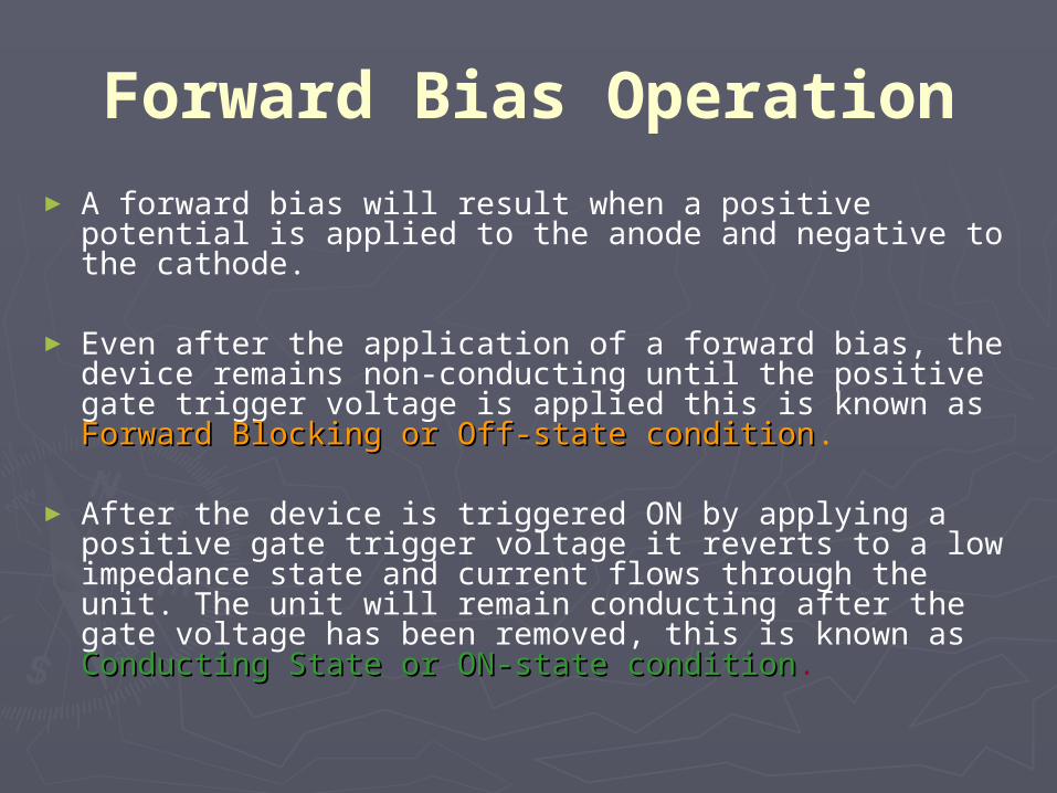
Two-Transistor model of Two-Transistor model of ThyristorThyristor
► Since Thyristor is a Latching device so the Since Thyristor is a Latching device so the regenerative or Latching action due to positive regenerative or Latching action due to positive feedback can be demonstrated by using a two feedback can be demonstrated by using a two transistor model of SCR.transistor model of SCR.
► A thyristor can be considered as two A thyristor can be considered as two complementary transistors, one is pnp -transistor complementary transistors, one is pnp -transistor Q1 and other is npn –transistorQ1 and other is npn –transistor
Q2.Q2.
► The circuit representation of the two-transistor model of a thyristor is shown in diagram.
DiagramDiagram

Contd.Contd.
► In the off state of a transistor, collector current IC is related to emitter current IE as-
…(1) ► where α is the common-base current gain and ICBO
is the common base leakage current of collector-base junction of a transistor with emitter open.
► For transistor Q1 in diagram, emitter current IE = anode current Ia and collector current Ic is Ic1. Therefore for transistor Q1,
…(2)

Contd.Contd.
► Similarly for transistor Q2, collector current IC2 is given by …(3)
► The sum of the two collector currents given by equations (2) and (3) is equal to the anode current Ia.
…(4) ► …(5)

Contd.Contd.► …(6)
…(7)
where Ik= (Ia + Ig)
► It is clear from eq. (7), that α1+α2 → 1 causes the thyristor to turn on i.e. the anode current reaches a high value or the SCR starts conducting.
► α1 varies with Ia (emitter current) and α2 varies with Ia+Ig. If Ig is increased, this increases Ia, which further increases α1 and α2. This will in turn increase Ia. This is a regenerative or positive feedback effect.

Phase Control of SCRPhase Control of SCR
► In SCR Phase Control, the firing angle, or point during the half-cycle at which the SCR is triggered, determines the amount of current which flows through the device as well as from the load.
► It acts as a high-speed switch which is open for the first part of the cycle, and then closes to allow power flow after the trigger pulse is applied.

Firing angelFiring angel

Contd.Contd.
► Figure shows an AC waveform being applied with a gating pulse at 45 degrees. There are 360 electrical degrees in a cycle; 180 degrees in a half-cycle.
►The number of degrees from the beginning of the cycle until the SCR is gated ON is referred to as the firing angle.
►The number of degrees that the SCR remains conducting is known as the conduction angle.

output voltageapplied to the load

Turning ON methods of SCRTurning ON methods of SCR
►There are five different methods There are five different methods
1) Thermal.1) Thermal.
2) Light.2) Light.
3) High voltage.3) High voltage.
4) High dv/dt rating.4) High dv/dt rating.
5) Gate current. (Most applicable)5) Gate current. (Most applicable)

Gate Current methodGate Current method
► This is the most widely used method to This is the most widely used method to turn-On the thyristor by applying a small turn-On the thyristor by applying a small positive gate signal to the SCR.positive gate signal to the SCR.
► As the gate current increased ,the forward As the gate current increased ,the forward blocking voltage (Vblocking voltage (VBOBO) is decreased.) is decreased.
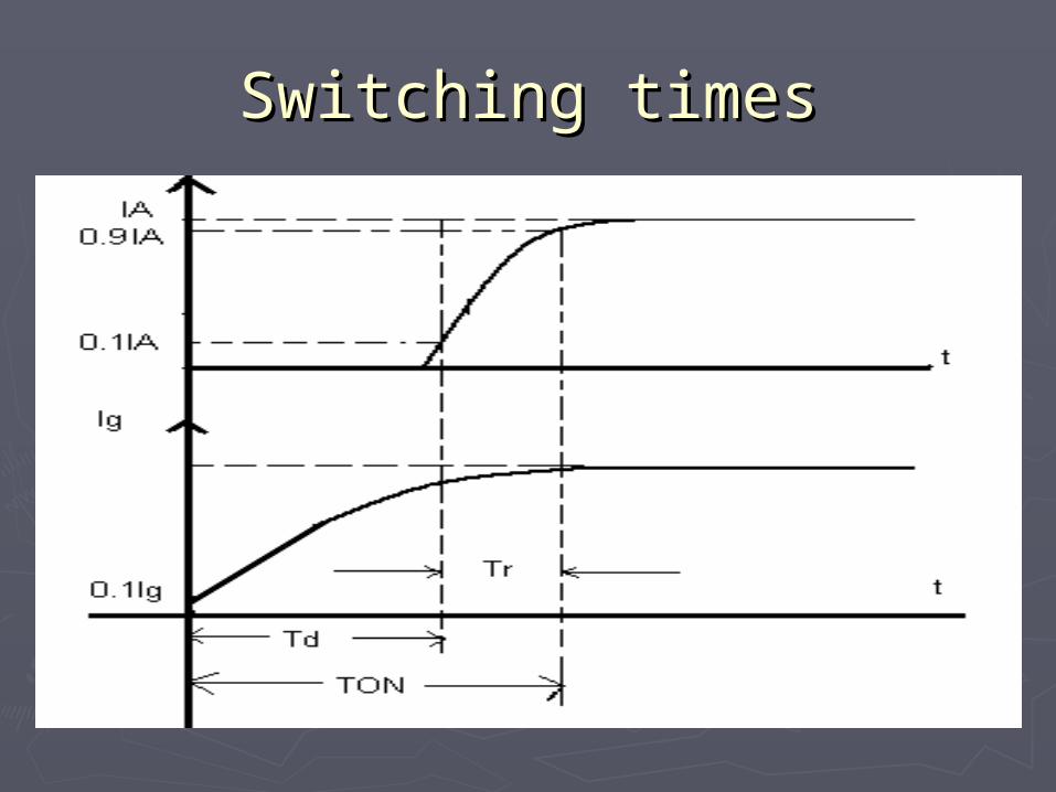
► The Turn-ON time The Turn-ON time (T(TONON)) of SCR is the sum of SCR is the sum
of Delay time of Delay time ((ttd)d) and Rise time and Rise time ((ttr).r).

Contd.Contd.
► Delay Time:Delay Time: It is defined as the time interval between It is defined as the time interval between
10% of the gate current and 10% of on-state Anode 10% of the gate current and 10% of on-state Anode current.current.
► Rise Time:Rise Time: It is the time interval between 10% of on-It is the time interval between 10% of on-
state current and 90% of on-state current.state current and 90% of on-state current.
Turn-On Time:Turn-On Time: It is the time interval between 10% of It is the time interval between 10% of
gate current and 90% of on-state anode current.gate current and 90% of on-state anode current.
Switching timesSwitching times

Application of SCRApplication of SCR
►Typical applications include :
1) DC motor control. 2) generator field regulation. 3) Variable Frequency Drive (VFD) DC
Bus voltage control. 4) Solid State Relays. 5) lighting system control.

ProblemsProblems
Q1:Q1:
Determine the minimum duration of gate Determine the minimum duration of gate pulse to turn the SCR On while Latching pulse to turn the SCR On while Latching current is 300mA, Input voltage 100V , current is 300mA, Input voltage 100V , R=20ohm, L=1H.R=20ohm, L=1H.
Q2:Q2:
Determine the value of Resistor to turn Off Determine the value of Resistor to turn Off Thyristor while Vs=330V and Holding Current Thyristor while Vs=330V and Holding Current is 150 mA. is 150 mA.

Types of ThyristorTypes of Thyristor
►Silicon Controlled Switch (SCS)Silicon Controlled Switch (SCS)►Mosfet controlled thyristor (MCT)Mosfet controlled thyristor (MCT)►Gate turn-Off Thyristor (GTO)Gate turn-Off Thyristor (GTO)►Reverse conducting thyristor (RCT)Reverse conducting thyristor (RCT)►A-symmetrical Thyristor (ASCR)A-symmetrical Thyristor (ASCR)

SILICON-CONTROLLED SILICON-CONTROLLED SWITCH SWITCH

Silicon-Controlled SwitchSilicon-Controlled Switch
► It is a four-layer pnpn deviceIt is a four-layer pnpn device► Its basic construction is the same with the SCR with Its basic construction is the same with the SCR with
the addition of the second gate terminal.the addition of the second gate terminal.► Terminals areTerminals are Anode, cathode, Anode gate Anode, cathode, Anode gate GaGa, and Cathode , and Cathode
gate gate GkGk..
Gate Terminal AdvantageGate Terminal AdvantageEffectEffect: The higher the anode gate current, the lower : The higher the anode gate current, the lower
the required anode-to-cathode voltage to turn the the required anode-to-cathode voltage to turn the device on.device on.
UseUse: Used to turn the device either on or off: Used to turn the device either on or off

PN
P
N
ANODE
ANODE GATE
CATHODE
CATHODE GATE
ANODE
ANODE GATE
CATHODE
CATHODE GATE
A.) SCS BASIC CONSTRUCTION
B.) SCS GRAPHIC SYMBOL
Symbol and ConstructionSymbol and Construction

Switching of SCSSwitching of SCS
►Turn on switching of the SCS is as Turn on switching of the SCS is as followsfollows
1) positive pulse on Gk terminal1) positive pulse on Gk terminal 2) negative pulse on Ga terminal2) negative pulse on Ga terminal
o Turn Off switching is as Turn Off switching is as
1) Negative pulse on Gk terminal1) Negative pulse on Gk terminal 2) Positive Pulse on Ga terminal2) Positive Pulse on Ga terminal

SCS equivalent transistor SCS equivalent transistor circuitcircuit
Anode gate
Anode
IC1
Q2
npn
GA
CathodeIGK
Cathode gate
Q1
pnp

OperationOperation
(To (To turn on the deviceturn on the device, a negative pulse must , a negative pulse must be applied to the be applied to the Anode gateAnode gate terminal, or terminal, or you can apply positive pulse on you can apply positive pulse on Cathode Cathode gategate terminal). terminal).
ON State: A negative pulse at the anode gate ON State: A negative pulse at the anode gate will forward-bias the base-to-emitter will forward-bias the base-to-emitter
junction of PNP Transistor junction of PNP Transistor QQ11 , turning it on. , turning it on.
The resulting heavy collector current IThe resulting heavy collector current IC1C1, ,
will turn on will turn on QQ2 2 , resulting in a , resulting in a regenerative regenerative actionaction and this will be the on state ( latching ) of the and this will be the on state ( latching ) of the
SCS device.SCS device.

Cont.Cont.
(To (To turn Off the deviceturn Off the device, a Positive pulse must , a Positive pulse must be applied to the be applied to the Anode gateAnode gate terminal, or you terminal, or you can apply negative pulse on can apply negative pulse on Cathode gateCathode gate terminal)terminal)
To turn OFFTo turn OFF: A positive pulse at the anode gate : A positive pulse at the anode gate will reverse-bias the base-to-emitter junction will reverse-bias the base-to-emitter junction of Qof Q11, turning it off, resulting in the open , turning it off, resulting in the open circuit”off” state of the device.circuit”off” state of the device.

ApplicationApplication
► SCS & SCR are Both used in similar Application.SCS & SCR are Both used in similar Application.
► SCS has complete control on Gate terminal which is SCS has complete control on Gate terminal which is used in both turn on & turn Off switching.used in both turn on & turn Off switching.
► The Voltage and Current ratings are more limited as The Voltage and Current ratings are more limited as compared to SCR.compared to SCR.
► It is used in Digital application such as counters, It is used in Digital application such as counters, registers & timing circuits.registers & timing circuits.

Mosfet controlled thyristor Mosfet controlled thyristor MCTMCT
► MOS Controlled ThyristorMOS Controlled Thyristor (or (or MCTMCT) is voltage ) is voltage controlled fully controllable controlled fully controllable ThyristorThyristor. .
► The MCT is similar in operation with GTO thyristor, The MCT is similar in operation with GTO thyristor, but it has voltage controlled insulated gate.but it has voltage controlled insulated gate.
► It has two MOSFETs in its equivalent circuit. One is It has two MOSFETs in its equivalent circuit. One is responsible for turn-on and the another is responsible for turn-on and the another is
responsible for turn-off.responsible for turn-off.

Types of MCTTypes of MCT
►There are basically two types of MCT There are basically two types of MCT
1) N type- Mosfet controlled thyristor 1) N type- Mosfet controlled thyristor
2) P type - Mosfet controlled thyristor 2) P type - Mosfet controlled thyristor

Equivalent Circuit & Circuit Equivalent Circuit & Circuit SymbolSymbol
P-MCT equivalent circuit P-MCT circuit symbol

N-MCT Equivalent Ckt & N-MCT Equivalent Ckt & SymbolSymbol
N-MCT equivalent circuit N-MCT circuit symbol

Turn-on switching of N-Turn-on switching of N-MCTMCT
Turn on MCT by turning on the ON-FET (Turn on MCT by turning on the ON-FET (n-Mosfetn-Mosfet))
• • Positive gate-cathode voltage for N-MCTPositive gate-cathode voltage for N-MCT
ON-FET delivers base current to the ON-FET delivers base current to the low-gain BJTlow-gain BJT in the in the thyristor equivalent circuit and activates that BJT.thyristor equivalent circuit and activates that BJT.
• • PNPPNP transistor in the N-MCT is Low gain BJT. transistor in the N-MCT is Low gain BJT.
Low-gain transistor activates the higher gain transistor Low-gain transistor activates the higher gain transistor NPNNPN and thyristor latches on.and thyristor latches on.
Once higher gain transistor Once higher gain transistor NPNNPN, which is in parallel with ON-, which is in parallel with ON-FET is activated, current is shunted from ON-FET to the BJT FET is activated, current is shunted from ON-FET to the BJT and the ON-FET carries very little current in the MCT on-state.and the ON-FET carries very little current in the MCT on-state.

Turn-Off switching of N-Turn-Off switching of N-MCTMCT
To Turn N-MCT off by turning on the OFF-FET (To Turn N-MCT off by turning on the OFF-FET (p-p-MosfetMosfet))
• • Negative gate-cathode input for the N-MCTNegative gate-cathode input for the N-MCT
OFF-FET shunts base current away from the OFF-FET shunts base current away from the higher higher gain BJTgain BJT in the thyristor equivalent circuit and in the thyristor equivalent circuit and forces it to cut-off.forces it to cut-off.
• • NPN transistor in the N-MCT is NPN transistor in the N-MCT is higher Gain BJThigher Gain BJT..
Cut-off of higher gain BJT then forces Cut-off of higher gain BJT then forces low-gain BJTlow-gain BJT into cut-off. So that MCT will turn Off.into cut-off. So that MCT will turn Off.

Gate Turn-off Thyristors GTOGate Turn-off Thyristors GTO
► The GTO is a non latching deviceThe GTO is a non latching device
► Turned on by applying positive gate signal.Turned on by applying positive gate signal.
► Turned off by applying negative gate signal.Turned off by applying negative gate signal.
► On state voltage is 3.4V for 550A, 1200V GTO.On state voltage is 3.4V for 550A, 1200V GTO.
► Controllable peak on-state current Controllable peak on-state current IITGQTGQ , is the peak , is the peak value of on-state current which can be turned-off by value of on-state current which can be turned-off by gate control.gate control.

Symbol, Cross section and Symbol, Cross section and Equivalent CircuitEquivalent Circuit

OperationOperation
► The turn on mechanism of GTO is similar to that of The turn on mechanism of GTO is similar to that of Conventional thyristor.Conventional thyristor.
► Gate current is maintained throughout the whole Gate current is maintained throughout the whole conduction period to prevent any drop out from the conduction period to prevent any drop out from the conduction state.conduction state.
► While in turn Off, the GTO has a relatively While in turn Off, the GTO has a relatively low gainlow gain that’s why it requires high reverse current on the that’s why it requires high reverse current on the Gate to turn the device Off. Gate to turn the device Off.
► When negative gate signal is applied than sufficient When negative gate signal is applied than sufficient charge carriers from the cathode terminal is charge carriers from the cathode terminal is removed and device drawn out from regenerative removed and device drawn out from regenerative action.action.

Characteristics CurveCharacteristics Curve

Advantage of GTO over SCR Advantage of GTO over SCR
► Elimination of commutating components in forced Elimination of commutating components in forced commutation resulting in reduction in cost, weight commutation resulting in reduction in cost, weight and volume.and volume.
► Faster turn OFF permitting high switching Faster turn OFF permitting high switching frequency.frequency.
► Improved converters efficiency.Improved converters efficiency.
► GTOs are GTOs are sensitivesensitive to to dv/dtdv/dt. Therefore, . Therefore, snubber snubber circuits are used to minimize dv/dt and di/dt rating circuits are used to minimize dv/dt and di/dt rating effects.effects.
► It can be used at high power levels.It can be used at high power levels.
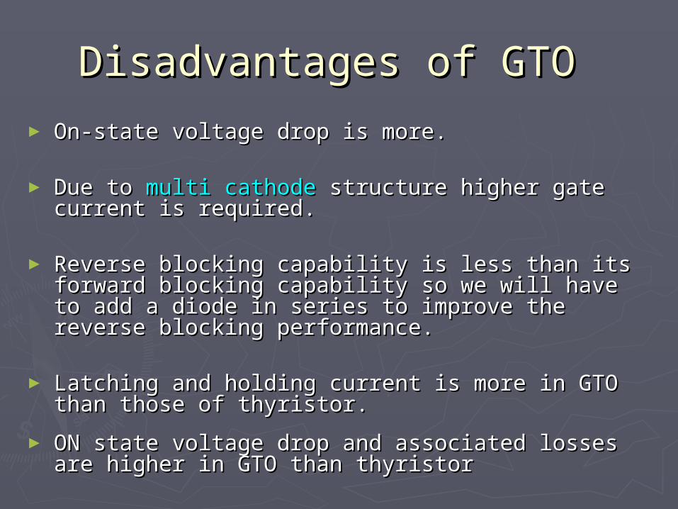
Disadvantages of GTO Disadvantages of GTO
► On-state voltage drop is more.On-state voltage drop is more.
► Due to Due to multi cathodemulti cathode structure higher gate current structure higher gate current is required.is required.
► Reverse blocking capability is less than its forward Reverse blocking capability is less than its forward blocking capability so we will have to add a diode in blocking capability so we will have to add a diode in series to improve the reverse blocking performance.series to improve the reverse blocking performance.
► Latching and holding current is more in GTO than Latching and holding current is more in GTO than those of thyristor.those of thyristor.
► ON state voltage drop and associated losses are ON state voltage drop and associated losses are higher in GTO than thyristorhigher in GTO than thyristor

Reverse Conducting ThyristorReverse Conducting Thyristor
► Reverse conducting thyristorReverse conducting thyristor (RCT) is high- (RCT) is high-power switching power switching semiconductor device similar to similar to thyristor with integrated reverse diode .thyristor with integrated reverse diode .
► This thyristor is not capable of This thyristor is not capable of reverse blockingreverse blocking mode. mode.
► The forward blocking voltage varies from 400 to The forward blocking voltage varies from 400 to 2000V.2000V.
► These devices are advantageous where These devices are advantageous where reversereverse or or freewheel diodefreewheel diode must be used. must be used.
Contd.Contd.
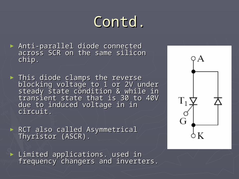
► Anti-parallel diode connected Anti-parallel diode connected across SCR on the same silicon across SCR on the same silicon chip.chip.
► This diode clamps the reverse This diode clamps the reverse blocking voltage to 1 or 2V under blocking voltage to 1 or 2V under steady state condition & while in steady state condition & while in transient state that is 30 to 40V transient state that is 30 to 40V due to induced voltage in in due to induced voltage in in circuit.circuit.
► RCT also called Asymmetrical RCT also called Asymmetrical Thyristor (ASCR).Thyristor (ASCR).
► Limited applications. used in Limited applications. used in frequency changers and inverters. frequency changers and inverters.

Breakover DevicesBreakover Devices
► The Breakover devices are used to apply the The Breakover devices are used to apply the triggering pulse to devices such as triggering pulse to devices such as SCRSCR and and TRIACTRIAC..
► There are three types of Breakover devicesThere are three types of Breakover devices
1) DIAC1) DIAC 2) UJT2) UJT 3) PUT3) PUT
• . .

DIACDIAC
• Bi-directional device without a gate terminal.Bi-directional device without a gate terminal.• DIAC is a five layer device PNPNP.DIAC is a five layer device PNPNP.• Conducts in both directions but waits for a Conducts in both directions but waits for a
breakover voltage.breakover voltage.• Breakover voltagesBreakover voltages are always the same in both are always the same in both
direction and not controllable.direction and not controllable.• DIACs are also called DIACs are also called symmetrical trigger diodessymmetrical trigger diodes
due to the symmetry of their characteristic curve. due to the symmetry of their characteristic curve. • Excellent for controlling TRIACExcellent for controlling TRIAC

DIAC voltage domain Current DIAC voltage domain Current RelationshipRelationship

OperationOperation
► The The DIACDIAC, or , or diode for alternating currentdiode for alternating current, is a , is a bidirectional trigger diode that conducts current only bidirectional trigger diode that conducts current only after its breakdown voltage has been exceeded. after its breakdown voltage has been exceeded.
► When this occurs, the resistance of the diode abruptly When this occurs, the resistance of the diode abruptly decreases, leading to a sharp decrease in the voltage decreases, leading to a sharp decrease in the voltage drop across the diode and, usually, a sharp increase in drop across the diode and, usually, a sharp increase in current flow through the diode. current flow through the diode.
► The terms anode and cathode no longer apply, so the The terms anode and cathode no longer apply, so the connections are simply named terminal 1connections are simply named terminal 1 (T1) (T1) and and terminal terminal 2 (T2)2 (T2). Each terminal can serve as either anode . Each terminal can serve as either anode or cathode, according to the polarity of the applied or cathode, according to the polarity of the applied voltage.voltage.

ContinuedContinued
► The diode remains "The diode remains "in conductionin conduction" until the current " until the current flowing through it drops below a certain current flowing through it drops below a certain current value, called the value, called the holding currentholding current. Below this value, . Below this value, the diode switches back to its the diode switches back to its high-resistancehigh-resistance ( (non-non-conductingconducting) state.) state.
► When used in AC applications this commutation is When used in AC applications this commutation is automatically happens when the current reverses automatically happens when the current reverses polarity. polarity.
► The drawback of the DIAC is that it cannot be The drawback of the DIAC is that it cannot be triggered at just any point in the ac power cycle; it triggered at just any point in the ac power cycle; it triggers at its preset breakover voltage only.triggers at its preset breakover voltage only.

DIAC - ApplicationDIAC - Application
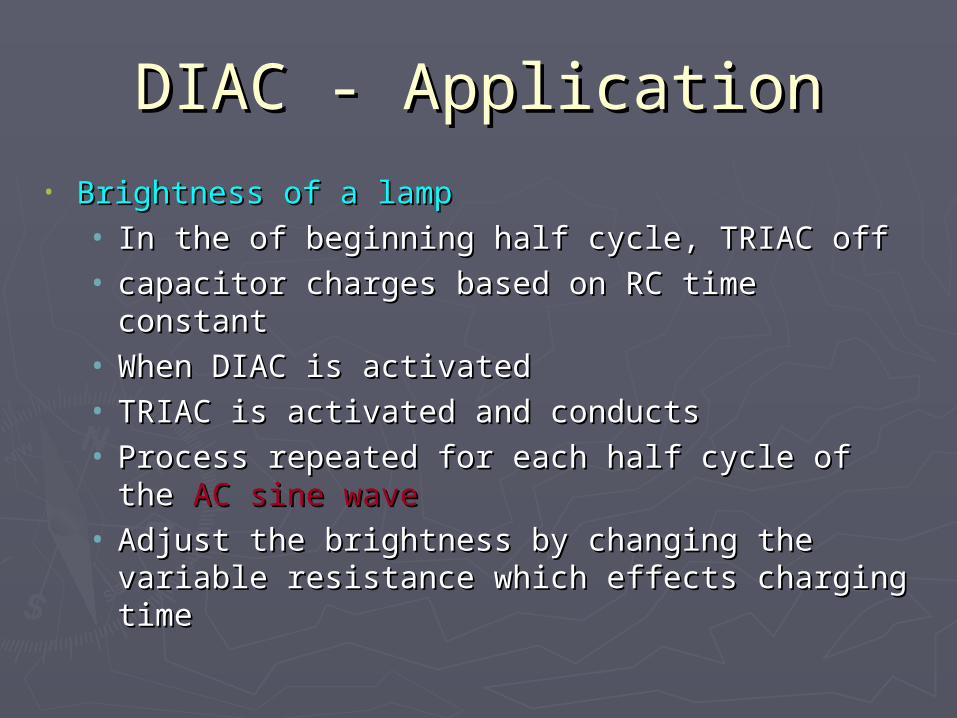
DIAC - ApplicationDIAC - Application• Brightness of a lampBrightness of a lamp
• In the of beginning half cycle, TRIAC offIn the of beginning half cycle, TRIAC off• capacitor charges based on RC time constantcapacitor charges based on RC time constant• When DIAC is activatedWhen DIAC is activated• TRIAC is activated and conductsTRIAC is activated and conducts• Process repeated for each half cycle of the Process repeated for each half cycle of the AC AC
sine wavesine wave• Adjust the brightness by changing the variable Adjust the brightness by changing the variable
resistance which effects charging timeresistance which effects charging time

UniJunction Transistor UniJunction Transistor UJTUJT
► A A Unijunction transistorUnijunction transistor ( (UJTUJT) is an ) is an electronic semiconductor device that is used electronic semiconductor device that is used to trigger the device such as SCR. to trigger the device such as SCR.
► The UJT does not belong to thyristor family The UJT does not belong to thyristor family because it does not have the because it does not have the four layerfour layer construction.construction.
► The term Unijunction refers to that the UJT The term Unijunction refers to that the UJT has a single has a single pn junctionpn junction..

Symbol & TerminalsSymbol & Terminals
► The UJT has three terminals: an The UJT has three terminals: an emitter (E) and two bases (B1 emitter (E) and two bases (B1 and B2). and B2).
► The base is formed by lightly The base is formed by lightly doped doped n-typen-type bar of silicon. Two bar of silicon. Two ohmic contacts ohmic contacts B1B1 and and B2B2 are are attached at its ends. attached at its ends.
► The emitter is of The emitter is of p-type p-type and it is and it is heavily doped.heavily doped.
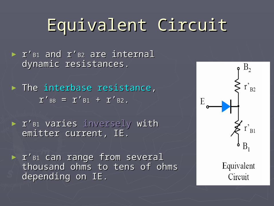
Equivalent CircuitEquivalent Circuit
► r’r’B1B1 and r’ and r’B2B2 are internal dynamic are internal dynamic resistances.resistances.
► The The interbase resistanceinterbase resistance,, r’r’BBBB = r’ = r’B1B1 + r’ + r’B2B2..
► r’r’B1B1 varies varies inverselyinversely with emitter with emitter current, IE.current, IE.
► r’r’B1B1 can range from several thousand can range from several thousand ohms to tens of ohms depending on ohms to tens of ohms depending on IE.IE.

Basic UJT BiasingBasic UJT Biasing VVr’B1r’B1 = ηV = ηVBBBB
η = (r’η = (r’B1B1/r’/r’BBBB) is the ) is the standoff ratio.standoff ratio.
If VIf VEB1EB1 < V < Vr’B1r’B1 + Vpn, then + Vpn, then IE = 0 since pn junction is not forward IE = 0 since pn junction is not forward
Biased.Biased.
At VAt VEB1=EB1=Vp = ηVBB + Vpn, the UJT Vp = ηVBB + Vpn, the UJT turns on and operates in a turns on and operates in a negative negative resistanceresistance region up to a certain region up to a certain value of emitter current.value of emitter current.
► It then becomes saturated at Valley It then becomes saturated at Valley point and point and IEIE increases with increases with VVE E
simultaneouslysimultaneously..

UJT Characteristic CurveUJT Characteristic Curve

Applications of UJTApplications of UJT
► UJT can be used as trigger UJT can be used as trigger device for SCR.device for SCR.
► The UJT is also used as a The UJT is also used as a Relaxation OscillatorRelaxation Oscillator..
► A A relaxation oscillatorrelaxation oscillator is an is an oscillator in which a capacitor is oscillator in which a capacitor is charged gradually and then charged gradually and then discharged rapidly.discharged rapidly.
► Other applications include Other applications include nonsinusoidal oscillatorsnonsinusoidal oscillators, , sawtooth generatorssawtooth generators, and , and timing circuits.timing circuits.

Conditions For UJT Relaxation Conditions For UJT Relaxation Oscillator OperationOscillator Operation
In the relaxation oscillator, Condition 1:• RE must not limit IE at the peak point to less than IP at turn-on, i.e., [ VBB - IP RE > Vp] Condition 2:• To ensure turn-off of the UJT at the valley point, RE must be large enough so that IE can decrease below Iv, i.e., [ VBB - IV RE < Vv]

Waveform of OscillatorWaveform of Oscillator

Oscillation FrequencyOscillation Frequency

Charging cycle Charging cycle
)1)(( 1t
lowHiLowc eVVVV
)1)(( )*( CR
t
vBBvcEeVVVV
))( )*( CR
t
vBBvBBvcEeVVVVVV
)())( )*( AeVVVV CR
t
vBBBBcE

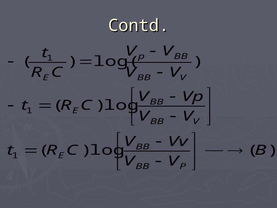
Contd.Contd.• Since Capacitor is charging so (Vc= Vp) Since Capacitor is charging so (Vc= Vp)
and (t=t1)and (t=t1)
)log()(
)log()log(
))(
))(
1
)1
(
)*(
)*(
1
1
VBB
BBp
E
VBB
BBpCR
t
CR
t
vBBBBP
CR
t
vBBBBP
VV
VV
CR
t
VV
VVe
eVVVV
eVVVV
E
E
E
Contd.Contd.
)(log)(
log)(
)log()(
1
1
1
BVV
VvVCRt
VV
VpVCRt
VV
VV
CR
t
PBB
BBE
VBB
BBE
VBB
BBp
E

Discharging cycleDischarging cycle
)log()(
))(((&).(
11
2
)(
)(
112
11
2
11
2
2
2
P
V
B
P
VCRr
t
CRr
t
pV
BVC
t
pC
V
V
CRr
t
V
Ve
eVV
CRrVVSince
eVV
B
B

Contd.Contd.
Tf
ttT
CV
VCRrt
V
V
CRr
t
V
pB
P
V
B
1
)(
)(log()(
)log()(
21
112
11
2

Programmable Unijunction Programmable Unijunction Transistor Transistor PUTPUT
► The PUT is actually a type of thyristor and a four The PUT is actually a type of thyristor and a four layer device.layer device.
► It can replace the UJT in some oscillator It can replace the UJT in some oscillator applications.applications.
► It is more similar to an SCR except that its anode to It is more similar to an SCR except that its anode to gate gate VVGG voltage can be used to both voltage can be used to both turn onturn on and and
turn offturn off the device. the device.
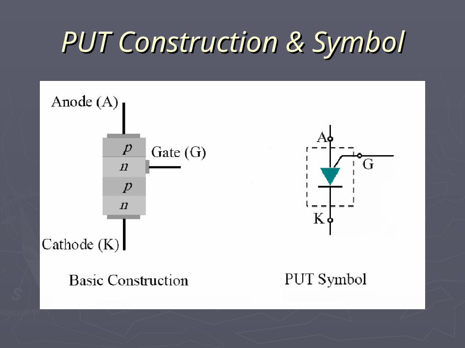
PUT Construction & SymbolPUT Construction & Symbol

Conditions of OperationConditions of Operation
►Notice that the gate is connected to the Notice that the gate is connected to the n n region adjacent to the anode.region adjacent to the anode.
► The gate is always positive with respect to The gate is always positive with respect to the cathode.the cathode.
► The standoff ratio is replaced by external The standoff ratio is replaced by external elements to program Velements to program VP P that's why it is called that's why it is called programmableprogrammable..
► The characteristic plot of The characteristic plot of VVAKAK versus versus IIAA is is similar to the similar to the VVEE versus versus IIEE plot of the UJT. plot of the UJT.

Cont.Cont.
►(V(VA – A – VVGG)) > > 0.70.7
WhereWhere VVA A is the is the anode to anode to Cathode voltageCathode voltage & & VVG G is is Gate voltage.Gate voltage.
► VVG G is the voltages that are is the voltages that are across the across the RR33 that can be that can be programmed by changing programmed by changing the the stand off ratiostand off ratio that that depends upon depends upon RR22 & & RR33 combination externally.combination externally.
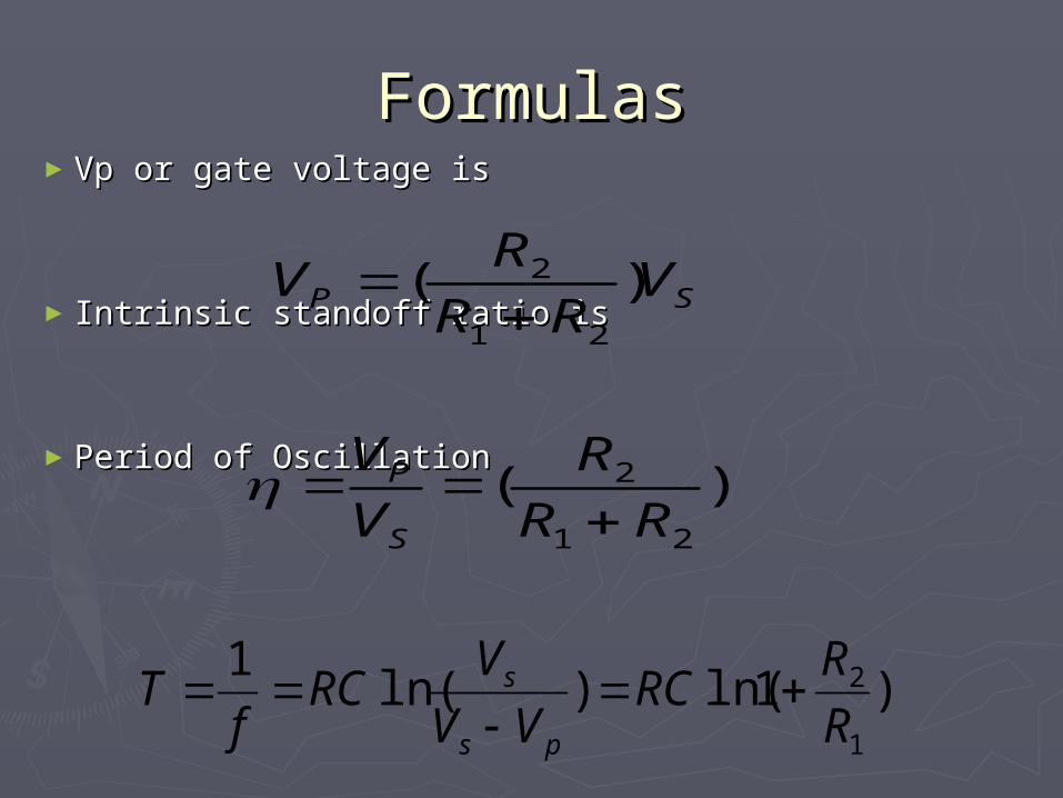
FormulasFormulas►Vp or gate voltage isVp or gate voltage is
► Intrinsic standoff ratio isIntrinsic standoff ratio is
►Period of OscillationPeriod of Oscillation
SP VRR
RV )(
21
2
)(21
2
RR
R
V
V
S
P
)1ln()ln(1
1
2
R
RRC
VV
VRC
fT
ps
s

PUTPUT Characteristics Curve Characteristics Curve

PUT as Relaxation OscillatorPUT as Relaxation Oscillator

Advantages over UJTAdvantages over UJT
► RRG1VG1V can control the frequency of oscillation with a can control the frequency of oscillation with a constant charging rate.constant charging rate.
► Can operate from lower supply voltages compared to Can operate from lower supply voltages compared to UJT. UJT.
► In case of UJT the In case of UJT the peak voltagespeak voltages are constant for are constant for
certain supply voltage while in PUT the peak voltage certain supply voltage while in PUT the peak voltage are depend upon the User. We can select peak are depend upon the User. We can select peak current and voltage for different values of Supply current and voltage for different values of Supply voltage. voltage.
► Can be used for very Can be used for very low frequencieslow frequencies that is because that is because the availability of lower Ithe availability of lower IP.P.
Related Documents