Noname manuscript No. (will be inserted by the editor) Power Consumption Evaluation of All-Optical Data Center Networks Christoforos Kachris · Ioannis Tomkos Received: date / Accepted: date Abstract Cloud computing and web emerging applications have created the need for more powerful data centers. These data centers need high bandwidth intercon- nects that can sustain the high interaction between the web-, application- and database-servers. Data center networks based on electronic packet switches will have to consume excessive power in order to satisfy the required communication bandwidth of future data centers. Optical interconnects have gained attention recently as a promising energy efficient solution offering high throughput, low la- tency and reduced energy consumption compared to current networks based on commodity switches. This paper presents a comparison on the power consumption of several optical interconnection schemes based on AWGRs, Wavelength Selec- tive Switches (WSS) or Semiconductor Optical Amplifiers (SOAs). Based on a thorough analysis of each architecture, it is shown that optical interconnects can achieve at least an order of magnitude higher energy efficiency compared to cur- rent data center networks based on electrical packet based switches and they could contribute to greener IT network infrastructures. Keywords Optical interconnects · data center networks · cluster networks · Green IT networks Athens Information Technology 19.5 Markopoulou av. Peania, 19005, Greece E-mail: [email protected], [email protected]

Welcome message from author
This document is posted to help you gain knowledge. Please leave a comment to let me know what you think about it! Share it to your friends and learn new things together.
Transcript

Noname manuscript No.(will be inserted by the editor)
Power Consumption Evaluation of All-Optical Data
Center Networks
Christoforos Kachris · Ioannis Tomkos
Received: date / Accepted: date
Abstract Cloud computing and web emerging applications have created the need
for more powerful data centers. These data centers need high bandwidth intercon-
nects that can sustain the high interaction between the web-, application- and
database-servers. Data center networks based on electronic packet switches will
have to consume excessive power in order to satisfy the required communication
bandwidth of future data centers. Optical interconnects have gained attention
recently as a promising energy efficient solution offering high throughput, low la-
tency and reduced energy consumption compared to current networks based on
commodity switches. This paper presents a comparison on the power consumption
of several optical interconnection schemes based on AWGRs, Wavelength Selec-
tive Switches (WSS) or Semiconductor Optical Amplifiers (SOAs). Based on a
thorough analysis of each architecture, it is shown that optical interconnects can
achieve at least an order of magnitude higher energy efficiency compared to cur-
rent data center networks based on electrical packet based switches and they could
contribute to greener IT network infrastructures.
Keywords Optical interconnects · data center networks · cluster networks ·Green IT networks
Athens Information Technology19.5 Markopoulou av. Peania, 19005, GreeceE-mail: [email protected], [email protected]

2 Christoforos Kachris, Ioannis Tomkos
1 Introduction
The exponential increase of the Internet traffic over the last few years, mainly
driven from emerging applications like streaming video, social networking and
cloud computing, has created the need for more powerful data centers. The appli-
cations that are hosted in the data centers require high interaction between the
web-, application and database-servers. For example, a common software frame-
work that is running on many data centers is MapReduce [19] in which jobs are
dispatched to many servers for parallel computing and then the results are col-
lected in a central server for port-processing. But this scheme poses a significant
challenge to the networking of the data centers creating the need for more effi-
cient interconnection schemes with high communication bandwidth and reduced
latency. The servers must experience a low latency communication among each
other but at the same time the total power consumption must remain low due to
thermal constraints [40].
Therefore, one of the most challenging issues in the design of a data center is
the power consumption. According to some studies [2], the power consumption of
the global data centers in 2007 was 330 billion kWh. Without changes in electric-
ity consumption and improved efficiency, this report estimated that data center’s
power consumption will exceed 1000 billion kWh by 2020 (which translates to 257
MtCO2 gas emission [9]). The servers in the data centers consume around 40%
of the total power, storage up to 37% and the network devices consume around
23% of the total IT power [4]. If the future data center networks continue to be
based on electronic packet switches, they will not be able to affordable satisfy the
required communication bandwidth of emerging applications without consuming
excessive power.
In order to face this increased communication bandwidth demand and the
power consumption constraints in the data centers, new interconnection schemes
must be developed that can provide high throughput, low latency and reduced
power consumption. Currently, optical technology is only utilized in data cen-

Power Consumption Evaluation of All-Optical Data Center Networks 3
ters for point-to-point links (opaque networks). These links are based on low cost
multi-mode fibers (MMF) for short-reach communication and are used for the
connections of the switches using fiber-based SFP (1Gbps) or SFP+ (10Gbps)
transceivers displacing the cooper-based cables [31]. In the near future higher
bandwidth transceivers are going to be adopted such as 4x10Gbps QSFP mod-
ules with four 10Gbps parallel optical channels and CXP modules with 12 parallel
10Gbps channels (Intel has also presented a 50Gbps silicon photonic transceiver
that can be used in data centers [12]).
The main drawback in this case is that power hungry electrical-to-optical (E/O)
and optical-to-electrical (O/E) transceivers are required since the switching is per-
formed using electronic packet switches. But as the data traffic in data centers is
increasing to Tbps, all-optical interconnects (in which the switching is performed at
the optical domain) could provide a viable solution to these systems. In telecommu-
nication networks, the replacement of opaque networks with all-optical networks
(e.g. lightpath bypass using ROADMs) has shown that can reduce significantly the
energy consumption [42]. Similarly, all-optical interconnects could meet the high
traffic requirements of the data center networks while decreasing significantly the
overall power consumption [23][34],[18][32].
This paper presents a thorough study on the power consumption of several
all-optical interconnection schemes for data centers that have appeared recently
in the research literature. Section II presents the optical technology and the com-
ponents that are used in the design of optical interconnects. Section III presents
the architectures of the optical interconnects and the analytical evaluation of the
power consumption. Finally, Section IV presents a quantitative comparison of the
optical interconnects based on current optical components and section V presents
the conclusions of this paper.
The main contributions of this paper are:
– A categorization of all-optical interconnects for data centers
– Analytic evaluation of the energy consumption of the optical architectures

4 Christoforos Kachris, Ioannis Tomkos
– Power consumption comparison between the different architectures and the
current data center networks using commodity switches
2 Optical Technology
The majority of the optical interconnections schemes presented in this paper are
based on modules that are widely used in optical telecommunication networks
(e.g. WDM networks and Passive optical networks (PONs)). This section describes
the basic optical modules that are utilized for the implementation of the optical
interconnects targeting data center networks[35].
– Couplers: A fiber optic coupler is a passive device that can distribute the
optical signal (power) from one fiber among two or more fibers. The fiber optic
coupler can also combine the optical signal from two or more fibers into a single
fiber.
– Arrayed-Waveguide Grating (AWG): AWGs are passive data-rate inde-
pendent optical devices that routes each wavelength of an input to a different
output (wavelength w of input i is routed to output [( i + w - 2) mod N]+1,
where N is the number of ports).
– Wavelength Selective Switch (WSS): A WSS is typically an 1xN optical
component than can partition the incoming set of wavelengths to different
ports (each wavelength or group of wavelengths can be assigned to be routed
to different port) [3].
– Micro-Electro-Mechanical Systems Switches (MEMS-switches): MEMS
optical switches are mechanical devices (MEMS) that physically rotate mirror
arrays redirecting the laser beam to establish a connection between the input
and the output. Because they are based on mechanical systems the reconfigu-
ration time is in the orders of a few milliseconds.
– Semiconductor Optical Amplifier (SOA): Semiconductor Optical Am-
plifiers are optical amplifiers that are based on silicon pn-junctions. Light is
amplified through stimulated emission when it propagates through the active
Power Consumption Evaluation of All-Optical Data Center Networks 5
region [38]. SOAs are generally preferred over other amplifiers due to their fast
switching time ( 1ns) and their energy efficiency [20].
– Tunable Wavelength Converters (TWC): A tunable wavelength converter
generates a configurable wavelength for an incoming optical signal. The tunable
wavelength converter includes a tunable laser, a SOA and a Mach-Zehnder
Interferometer (MZI). The conversion is performed by the SOA which receives
as an input the tunable laser wavelength and the data and outputs the data in
the selected wavelength. The current TWC can work up to 160Gbps and the
reconfiguration time is in the order of nanoseconds [36].
3 Architectures
This section presents the optical interconnects schemes that have been proposed for
data center networks. In this paper we examine only the optical interconnects that
are all-optical and are based on packet or frame-switching. There are several other
schemes (such as hybrid schemes) that are based on a combination of current data
center networks with optical networks [47][21]. These hybrid schemes utilize the
current data center networks for all-to-all communication, while they use circuit-
based optical networks for long-lived communication between racks that transfer
high amount of data. These hybrid schemes are mainly used to enhance the cur-
rent data center networks, while in this paper we study the all-optical schemes
that are targeting high bandwidth future data center networks. Some other op-
tical networks are based on optical circuit switching that are mainly targeting
high performance computing (HPC) in which bulky data transfers are required
between the computing nodes that justifies the reconfiguration overhead of the
circuit switching [15].
However, according to several studies, the network traffic characteristics of
the data centers are quite different than the HPC. According to these studies
([30][17][16]) the average traffic flow size in the data center are considerably small
(i.e. less than 10KB) and a significant fraction of these flows last under a few

6 Christoforos Kachris, Ioannis Tomkos
hundreds of milliseconds. Furthermore, the packet size in data centers exhibit a
bimodal pattern with most packet sizes clustering around 200 and 1400 bytes.
This is due to the fact that the packets are either small control packets or are
parts of large files that are fragmented to the maximum packet size of the Eth-
ernet networks (1500 bytes). Furthermore, each server on the data center has a
limited number of active flows with other servers at any given session (e.g. the
web server is connected to a limited number of application and database servers
for each session). Based on these characteristics of the network traffic, optical in-
terconnects that are based on packet or burst switching can address the network
traffic fluctuations better than the circuit switching optical networks. Therefore,
this study examines mainly the optical interconnects that are based on packet or
burst switching.
In this section, we first present the current data center networks based on
commodity Ethernet switches and we discuss the communication requirements
between the servers in these networks. The optical interconnects are classified into
four categories. The first category is based on AWGR modules and three different
architectures are presented (AWGR with buffers, AWGR in Clos topology and
AWGR with time switch). The second category is based on Wavelength Selective
Switches (WSS), the third category is based on Broadcast and Select architectures
and the last category is based on bidirectional SOA modules.
3.1 Current DC with commodity switches
Current data centers are based on Ethernet packet-based switches for the inter-
connection network. The network is usually a canonical fat-tree 2-Tier or 3-Tier
architecture as it is depicted in Figure 1 [28]. The servers (usually up to 48 in
the form of blades) are accommodated into racks and are inter-connected through
a Top-of-the-Rack Switch (ToR) using 1Gbps links. These ToR switches are fur-
ther inter-connected through an aggregate switch using 10Gbps links (e.g. SFP+
transceivers) in a tree topology. In 3-Tier topologies, one more level is applied in

Power Consumption Evaluation of All-Optical Data Center Networks 7
which the aggregate switches are connected in a fat-tree topology using the core
switches either at 10Gbps or 40Gbps links (using a bundle of 10Gbps links, e.g.
QSFP) [7]. The main advantage of this architecture is that it can be scaled easily
and that it is fault tolerant (e.g. a ToR switch is usually connected to 2 or more
aggregate switches).
Coreswitches
… ToR
AggregateSwitch
10Gbps
… ToR
1Gbps
Rack Servers
Fig. 1 Architecture of current data center network
However, the main drawback of these architectures is the high power con-
sumption of the ToR, aggregate and core switches and the high number of links
that are required. The high power consumption of these switches is mainly due to
the power dissipation of the packet buffers (i.e. SDRAM), the switch fabrics and
the electrical-to-optical and optical-to-electrical transceivers [50]. Furthermore, a
significant drawback in the case of the current commodity switches is that the
power consumption of these devices is not directly proportional to the network

8 Christoforos Kachris, Ioannis Tomkos
traffic load. The power consumption of an idle switch is very close to the maxi-
mum power consumption when all of the ports are fully loaded which translates
to low energy efficiency [27]. Another problem of the current data center networks
is the latency introduced due to multiple store-and-forward processing. When a
packet travels from one server to another through the ToR, the aggregate and the
core switch it experiences significant queuing and processing delay in each switch.
Therefore, new energy-efficient interconnects are required that can sustain the high
communication bandwidth of the data centers with reduced power consumption.
3.2 AWGR-based Architecture
The first architecture that is presented is based on Arrayed-Waveguide Grating
Routing (AWGR) and tunable wavelength converters (TWC). In this architecture
the AWG is used as the switching module that allows contention resolution in
the wavelength domain. Each wavelength at the input port is routed to different
output, thus the nodes at the input ports select the transmitted wavelength based
on the destination ports. In this paper we explore three different architectures that
are based on AWGR-based optical interconnects.
3.2.1 AWGR-based with Buffer
The first AWGR architecture that is presented is based on AWGR for the routing
of the packet, an array of TWC in the input ports and a shared buffer. University
of California, Davis has presented an optical network based on this scheme, called
DOS (Scalable Datacenter Optical Switch) [51]. Figure 2 depicts the high level
block diagram of the DOS architecture.
The optical switch fabric consists of an array of tunable wavelength convert-
ers (TWC)(one TWC for each node), an AWGR and a loopback shared buffer.
Each node (i.e. ToR switch) can access any other node through the AWGR by
configuring the transmitting wavelength of the TWC. The switch fabric is config-
ured by the control plane that controls the TWC and the label extractors (LEs).

Power Consumption Evaluation of All-Optical Data Center Networks 9
The control plane is used for the contention resolution and TWC tuning. When
a node transmits a packet to the switch, the label extractors are used to separate
the optical label from the optical payload. The optical label (that includes the
destination address) is converted to electrical signal by an O/E converted inside
the control plane module and it is forwarded to the arbitration unit. The label
includes both the destination address and the packet length. This label is stored
in the label processor and this processor sends a request to the arbitration unit
for content resolution. Based on the decision by the arbitration unit, the control
plane configures accordingly the TWC.
ControlPlane
ToRswitches
…
TWC
TWC
LE
LE
SDRAMBuffer
O/EO/E
O/EO/E
O/EO/E
O/EO/E
AWGRTWCLE
TWC
BufferO/EO/EO/EO/E
Controller
Fig. 2 AWGR with Buffer: The DOS architecture
When the number of output receivers is less than the number of nodes that want
to transmit to this port, a link contention occurs. In this case, a shared SDRAM
buffer is used to store temporarily the transmitted packets. The wavelengths that
face the contention are routed to the SDRAM through an optical-to-electrical
(O/E) converter. The packets are then stored in SDRAM and a Shared buffer

10 Christoforos Kachris, Ioannis Tomkos
controller is used to handle these packets. This controller sends the requests of
the buffered packets to the control plane and waits for a grant. When the grant
is received, the packet is retrieved from the SDRAM, converted back to optical
signal through an electrical-to-optical converter and then it is forwarded to the
switch fabric through a TWC.
The main challenge is the deployment of the DOS switch is the arbitration of
the requests in the control plane. Since, there are not used virtual output queues
(VOQ), every input issues a request to the arbiter and waits for the grant. The
scalability of the DOS scheme depends on the scalability of the AWGR and the
tunability of the TWC. Some research papers have presented AWGR that can
reach up to 400 ports [26]. Thus single AWGR-based architectures, such as DOS,
could be used to connect soon up to 512 nodes (or 512 racks assuming that each
node is used as a ToR switch).
The main advantage of the AWGR-based with buffers scheme is that the la-
tency is almost independent of the number of input ports and remains low even at
high input loads. This is due to the fact that when there is no contention, then the
packets have to traverse only through an optical switch and they avoid the delay of
the electrical switch’s buffers. However the main drawback of this scheme is that
it is based on electrical buffers for the congestion management using power hungry
electrical-to-optical and optical-to-electrical converters, thus increasing the overall
power consumption and the packet latency.
A 40Gbps 8x8 prototype of the DOS architecture has been recently presented
by UCD and NPRC [37]. The prototype is based on an 8x8 200GHz spacing AWGR
and it also includes four wavelength converters (WC) based on cross-phase mod-
ulation (XPM) in a semiconductor optical amplifier Mach-Zehnder interferometer
(SOA-MZI). The measured switching latency of the DOS prototype was only 118.2
ns which is much lower compared to the latency of legacy data centers (i.e. in the
order of few microseconds).

Power Consumption Evaluation of All-Optical Data Center Networks 11
The total power consumption of the data plane on this architecture can be
calculated by measuring the power consumption of the optical transceivers, the
power consumption of the TWC and the power consumption of the Shared Buffer
(the shared buffer is used only when a contention occurs). Thus the total power
consumption of this architecture is:
PAWGR−Buffer =∑
PTRX +∑
PTWC +∑
PBuffer
= n · PTRX + n · PTWC+
a · n · (POE + PEO + PSDRAM ) (Eq.1)
where:
PTRX : Power of the Optical Transceiver
PTWC : Power of the Tunable Wavelength Converter
PShBuffer : Power of the Shared Buffer
POE,EO : Power of the O/E and E/O converters
PSDRAM : Power of the SDRAM
n : Number of ToR switches (nodes)
a : probability of contention (average: 20% according to [37])
As it was mention in the previous section the total power consumption of the
commodity switch when it is fully loaded is slightly larger than the power con-
sumption with almost zero traffic [27]. For example the power consumption of the
Cisco 3560V2 switch is 24W with 100% and 22W with 5% throughput [6]. Simi-
larly, the power consumption of the optical components (e.g. optical transceivers,
TWC, etc.) is almost independent of the network traffic load [5]. Therefore, in all
power equations we assume the same power consumption.

12 Christoforos Kachris, Ioannis Tomkos
IMs CMs OMs
Tunable TWC
TWC
NxNAWG
TWC
TWC
TWC
NxNAWG
TWC
TunableLaser
TunableLaser
TunableL
NxNAWG
TWC
NxNAWG
TWC
NxNAWG
NxNAWG
Laser
TunableLaser
Fig. 3 AWGR-Clos: The Petabit architecture
3.2.2 AWGR-Clos
To eliminate the need for packet buffering when a contention occurs, a Clos network
can be implemented using three stages of AWGRs. Jonathan Chao from Polytech-
nic Institute of New York has presented a scalable bufferless optical switch fabric,
called Petabit switch fabric, that is based on a Clos network of AWGR and tun-
able wavelength converters [49]. Figure 3 depicts the block diagram of the Petabit
optical switch. In the first stage, the tunable lasers are used to route the packets
through the AWGRs, while in the second and in the third stage TWC are used to
convert the wavelength and route accordingly the packets to destination port.
The main difference compared to the previous scheme is that this architecture
does not use any buffers inside the switch fabric (thus avoiding the power hungry
E/O and O/E conversion). Instead, the congestion management is performed us-
ing electronic buffers in the Line cards and an efficient scheduling algorithm. Each
line card that is connected to the input port of the Petabit switch hosts a buffer
in which the packet are stored before the transmission. The packets are classi-
fied to different virtual output queues (VOQ) based on the destination address.
Given the high number of ports, a VOQ is maintained per OM (the last stage
of the switch fabric) instead of one VOQ per output port. Using one VOQ per
OM simplifies the scheduling algorithm and the buffer management but on the
other hand it introduced Head-of-line blocking (HOL). However, using an efficient
scheduling algorithm and some speedup, the Petabit switch fabric can achieve

Power Consumption Evaluation of All-Optical Data Center Networks 13
100% throughput. The scheduler is used to find a bipartite match from the input
port to the output ports and assign a CM (the central stage of the switch fabric)
for each match such that the throughput is maximized. Using the bipartite match
scheduling, there is no congestion of the packets in the switch fabric thus the
buffer that is used in other schemes (e.g. in the DOS architecture) is eliminated.
The most important advantage of the proposed architecture is that the average
latency is only twice of a frame duration (200 ns) even at 80% load using three
iteration of the scheduling algorithm. Hence, in contrast with the current data
center networks based on commodity switches, the latency is significantly reduced
and almost independent of the switch size.
The power consumption of this architecture is based on the number of tunable
optical transceivers, and the number of tunable wavelength converters (TWC).
Tunable optical transceivers are commercially available today and can be tuned to
a wide range of wavelengths. However, the power consumption of these transceivers
are higher than the power consumption of the fixed wavelength transceivers. In
this scheme the number of TWC is twice the number of nodes thus the the total
power consumption of this architecture is:
PAWGR−Clos =∑
PT−TRX +∑
PTWC
= n · PT−TRX + 2 · n · PTWC (Eq.2)
where:
PT−TRX : Power of the Tunable Optical Transceiver
PTWC : Power of the Tunable Wavelength Converter
14 Christoforos Kachris, Ioannis Tomkos
3.2.3 AWGR-Clos with Time Switch
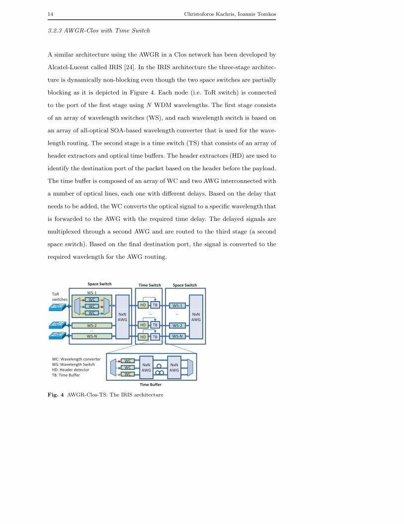
A similar architecture using the AWGR in a Clos network has been developed by
Alcatel-Lucent called IRIS [24]. In the IRIS architecture the three-stage architec-
ture is dynamically non-blocking even though the two space switches are partially
blocking as it is depicted in Figure 4. Each node (i.e. ToR switch) is connected
to the port of the first stage using N WDM wavelengths. The first stage consists
of an array of wavelength switches (WS), and each wavelength switch is based on
an array of all-optical SOA-based wavelength converter that is used for the wave-
length routing. The second stage is a time switch (TS) that consists of an array of
header extractors and optical time buffers. The header extractors (HD) are used to
identify the destination port of the packet based on the header before the payload.
The time buffer is composed of an array of WC and two AWG interconnected with
a number of optical lines, each one with different delays. Based on the delay that
needs to be added, the WC converts the optical signal to a specific wavelength that
is forwarded to the AWG with the required time delay. The delayed signals are
multiplexed through a second AWG and are routed to the third stage (a second
space switch). Based on the final destination port, the signal is converted to the
required wavelength for the AWG routing.
WC
WC
WS 1
HD TB WS 1
Space Switch Time Switch Space Switch
ToRswitches
WC
WS 2
WS N
NxNAWG
HD TB
HD TB
WS 2
WS N
NxNAWG
…
… …
WC
WC
WC
NxNAWG
NxNAWG
WC: Wavelength converterWS: Wavelength SwitchHD: Header detectorTB: Time Buffer
Time Buffer
Fig. 4 AWGR-Clos-TS: The IRIS architecture

Power Consumption Evaluation of All-Optical Data Center Networks 15
Due to the periodic operation of the third space switch, the scheduling is
local and deterministic to each time buffer which greatly reduces control-plane
complexity and removes the need for optical random access memory. Using 40
Gb/s data packets and 80x80 AWGs allows this architecture to scale to 802 × 40
Gbps = 256 Tbps.
The IRIS project has been prototyped using 4 XFP transceivers at 10Gbps
and has been implemented in an FPGA board. A 40 Gb/s wavelength converter is
used that is based on fully-integrated InP circuit with a SOA for the wavelength
conversion [43]. The wavelengths conversion takes less than 1ns.
The total power consumption of this architecture can be calculated by adding
the number of optical transceivers, and the number of tunable wavelength con-
verters. Unlike the Petastar architecture, in this case there are not used tunable
transceivers but the number of TWC is triple the number of nodes (the time switch
buffers in the second stage use also TWC). Therefore, the total power consumption
of this architecture is:
PTWC3 =∑
PTRX +∑
PTWC
= n · PTRX + 3 · n · PTWC (Eq.3)
where:
PTRX : Power of the Optical Transceiver
PTWC : Power of the Tunable Wavelength Converter
3.3 WSS-based Architecture
Another architecture for optical interconnects is based on Wavelength Selective
Switches (WSS). University of Illinois-UI and NEC have proposed the Proteus ar-
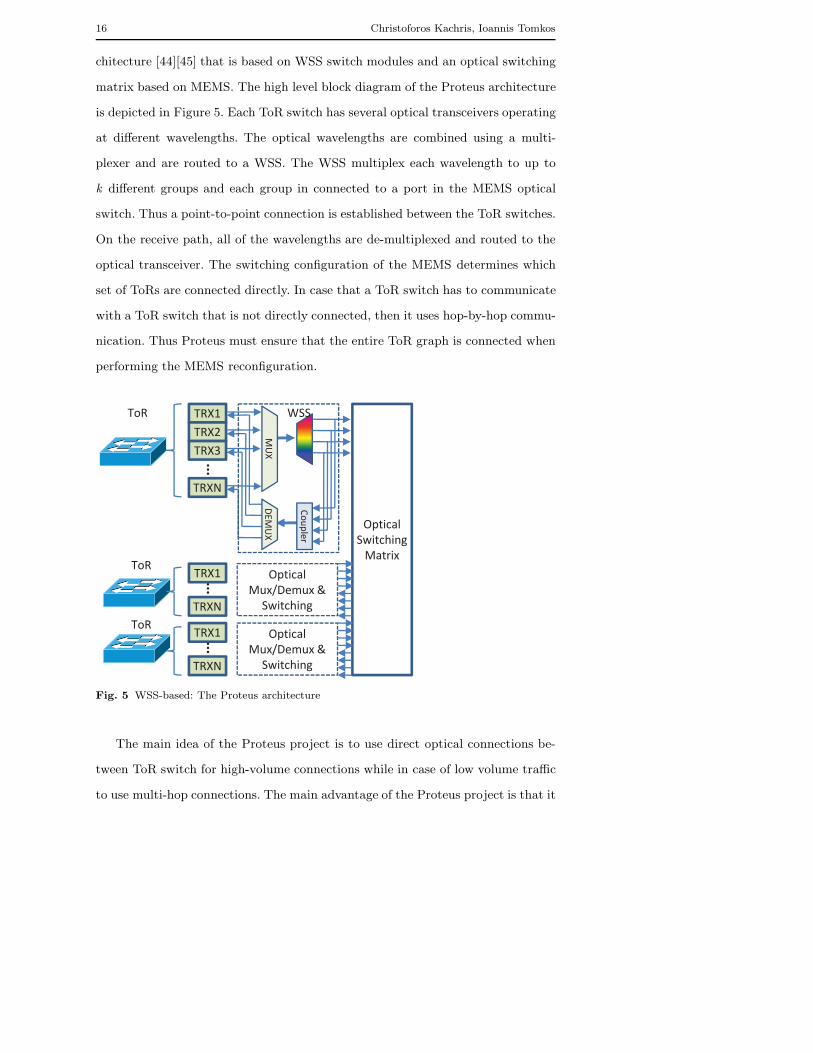
16 Christoforos Kachris, Ioannis Tomkos
chitecture [44][45] that is based on WSS switch modules and an optical switching
matrix based on MEMS. The high level block diagram of the Proteus architecture
is depicted in Figure 5. Each ToR switch has several optical transceivers operating
at different wavelengths. The optical wavelengths are combined using a multi-
plexer and are routed to a WSS. The WSS multiplex each wavelength to up to
k different groups and each group in connected to a port in the MEMS optical
switch. Thus a point-to-point connection is established between the ToR switches.
On the receive path, all of the wavelengths are de-multiplexed and routed to the
optical transceiver. The switching configuration of the MEMS determines which
set of ToRs are connected directly. In case that a ToR switch has to communicate
with a ToR switch that is not directly connected, then it uses hop-by-hop commu-
nication. Thus Proteus must ensure that the entire ToR graph is connected when
performing the MEMS reconfiguration.
TRX1TRX2
WSS
MUX
...
TRX3
ToR
TRXN
Coupler
DEM
UX
Optical
OpticalSwitchingMatrix
ToRTRX1 p
Mux/Demux &Switching
OpticalMux/Demux &
Switching
ToRTRXN
...
TRX1
TRXN
...
Fig. 5 WSS-based: The Proteus architecture
The main idea of the Proteus project is to use direct optical connections be-
tween ToR switch for high-volume connections while in case of low volume traffic
to use multi-hop connections. The main advantage of the Proteus project is that it
Power Consumption Evaluation of All-Optical Data Center Networks 17
can achieve coarse-grain flexible bandwidth. Each ToR has n optical transceivers.
If for some reason the traffic between two switches increase, then additional con-
nections can be set up (up to n, either directly or indirectly) thus increasing the
optical bandwidth up to n times the bandwidth of one optical transceiver. Another
advantage of this scheme is that although it is based on optical circuits using the
MEMS switches, it can achieve all-to-all communication using multi-hops routing
without the overhead of circuit reconfiguration.
The main challenge in the operation of the Proteus network is to find the opti-
mum configuration for the MEMS switch for each traffic pattern. In [44] an Integer
Linear Programming scheme is used to find the optimum configuration based on
the traffic requirements. The main advantage of the Proteus is that it is based
on readily available off-the-shelf optical modules (WSS such as the Finisar WSS
[3], and optical multiplexers) that are widely used in optical telecommunication
networks thus reducing the overall cost compared with ad-hoc solutions.
The main disadvantage of the Proteus architecture is that the MEMS switch
reconfiguration time is in the order of a few milliseconds. Thus, in applications
where the traffic flow changes rapidly and each server establishes connection with
other servers that last few milliseconds the proposed scheme will have to change
frequently the MEEMS switch to follow the traffic fluctuations. However, although
the traffic between the servers changes rapidly, the aggregated traffic between the
ToR switches may change much slower. In these cases, the Proteus scheme can
exhibit high performance and reduced latency.
The total power consumption of the WSS architecture is based on the number
of optical transceivers, the power consumption of the WSS and the power con-
sumption of the MEMS. Currently there are available WSS than can route up
to 96 different wavelengths and can support up to 9 ports [3]. The total power
consumption of this architecture is:

18 Christoforos Kachris, Ioannis Tomkos
PWSS =∑
PTRX +∑
PWSS +∑
PMEMS
= n ·Racks · PTRX + n · PWSS + 4 · n · PMEMS (Eq.4)
where:
n : Number of transceivers per node
PTRX : Power of the Optical Transceiver
PWSS : Power of the Wavelength Selective Switch
PMEMS : Power of the Optical Micro-Mechanical Systems
3.4 Broadcast and Select (B&S) Architecture
IBM and Corning have jointly developed the OSMOSIS project [33][25] that is low-
latency optical broadcast-and-select (B&S) architecture based on wavelength- and
space-division multiplexing. The broadcast-and-select architecture is composed of
two different stages. In the first stage each node transmits on a different wave-
length. These wavelengths are multiplexed in a common WDM line (up to 8 wave-
lengths per WDM link) and are broadcasted to all the modules of the second stage
through a coupler. The second stage uses SOAs as fiber-selector gates to select the
wavelength that will be forwarded to the output. However, in any configuration
only two SOAs are active in the each Select plane. Therefore for the case of 64
nodes shown in the figure, although there are 2048 SOAs, only 128 SOAs will be
active (the ones that have been selected based on the destination port).
In the framework of the OSMOSIS project a 64-node interconnect scheme has
been developed, combining eight wavelengths on eight fibers to achieve 64-way
distribution. The switching is achieved with a fast 8:1 fiber-selection stage followed
by a fast 8:1 wavelength-selection stage at each output port as it is depicted in
Power Consumption Evaluation of All-Optical Data Center Networks 19
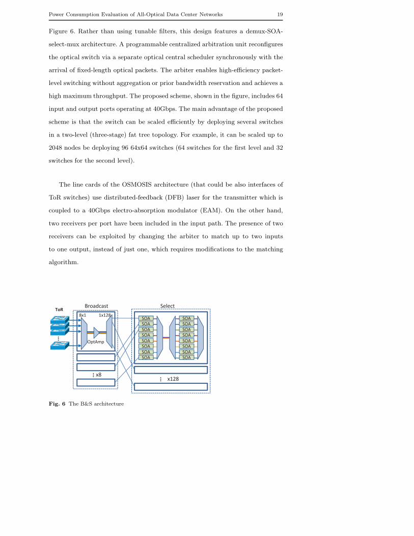
Figure 6. Rather than using tunable filters, this design features a demux-SOA-
select-mux architecture. A programmable centralized arbitration unit reconfigures
the optical switch via a separate optical central scheduler synchronously with the
arrival of fixed-length optical packets. The arbiter enables high-efficiency packet-
level switching without aggregation or prior bandwidth reservation and achieves a
high maximum throughput. The proposed scheme, shown in the figure, includes 64
input and output ports operating at 40Gbps. The main advantage of the proposed
scheme is that the switch can be scaled efficiently by deploying several switches
in a two-level (three-stage) fat tree topology. For example, it can be scaled up to
2048 nodes be deploying 96 64x64 switches (64 switches for the first level and 32
switches for the second level).
The line cards of the OSMOSIS architecture (that could be also interfaces of
ToR switches) use distributed-feedback (DFB) laser for the transmitter which is
coupled to a 40Gbps electro-absorption modulator (EAM). On the other hand,
two receivers per port have been included in the input path. The presence of two
receivers can be exploited by changing the arbiter to match up to two inputs
to one output, instead of just one, which requires modifications to the matching
algorithm.
SOASOASOA
SOASOASOA
8x1 1x128ToR
Broadcast Select
SOASOASOASOASOASOA
SOASOASOASOASOASOA
...
OptAmp
... x8x128
...
Fig. 6 The B&S architecture
20 Christoforos Kachris, Ioannis Tomkos
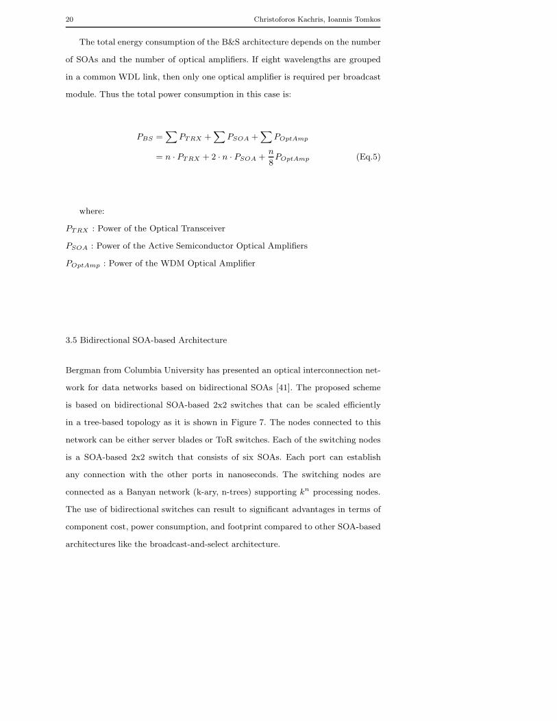
The total energy consumption of the B&S architecture depends on the number
of SOAs and the number of optical amplifiers. If eight wavelengths are grouped
in a common WDL link, then only one optical amplifier is required per broadcast
module. Thus the total power consumption in this case is:
PBS =∑
PTRX +∑
PSOA +∑
POptAmp
= n · PTRX + 2 · n · PSOA +n
8POptAmp (Eq.5)
where:
PTRX : Power of the Optical Transceiver
PSOA : Power of the Active Semiconductor Optical Amplifiers
POptAmp : Power of the WDM Optical Amplifier
3.5 Bidirectional SOA-based Architecture
Bergman from Columbia University has presented an optical interconnection net-
work for data networks based on bidirectional SOAs [41]. The proposed scheme
is based on bidirectional SOA-based 2x2 switches that can be scaled efficiently
in a tree-based topology as it is shown in Figure 7. The nodes connected to this
network can be either server blades or ToR switches. Each of the switching nodes
is a SOA-based 2x2 switch that consists of six SOAs. Each port can establish
any connection with the other ports in nanoseconds. The switching nodes are
connected as a Banyan network (k-ary, n-trees) supporting kn processing nodes.
The use of bidirectional switches can result to significant advantages in terms of
component cost, power consumption, and footprint compared to other SOA-based
architectures like the broadcast-and-select architecture.
Power Consumption Evaluation of All-Optical Data Center Networks 21
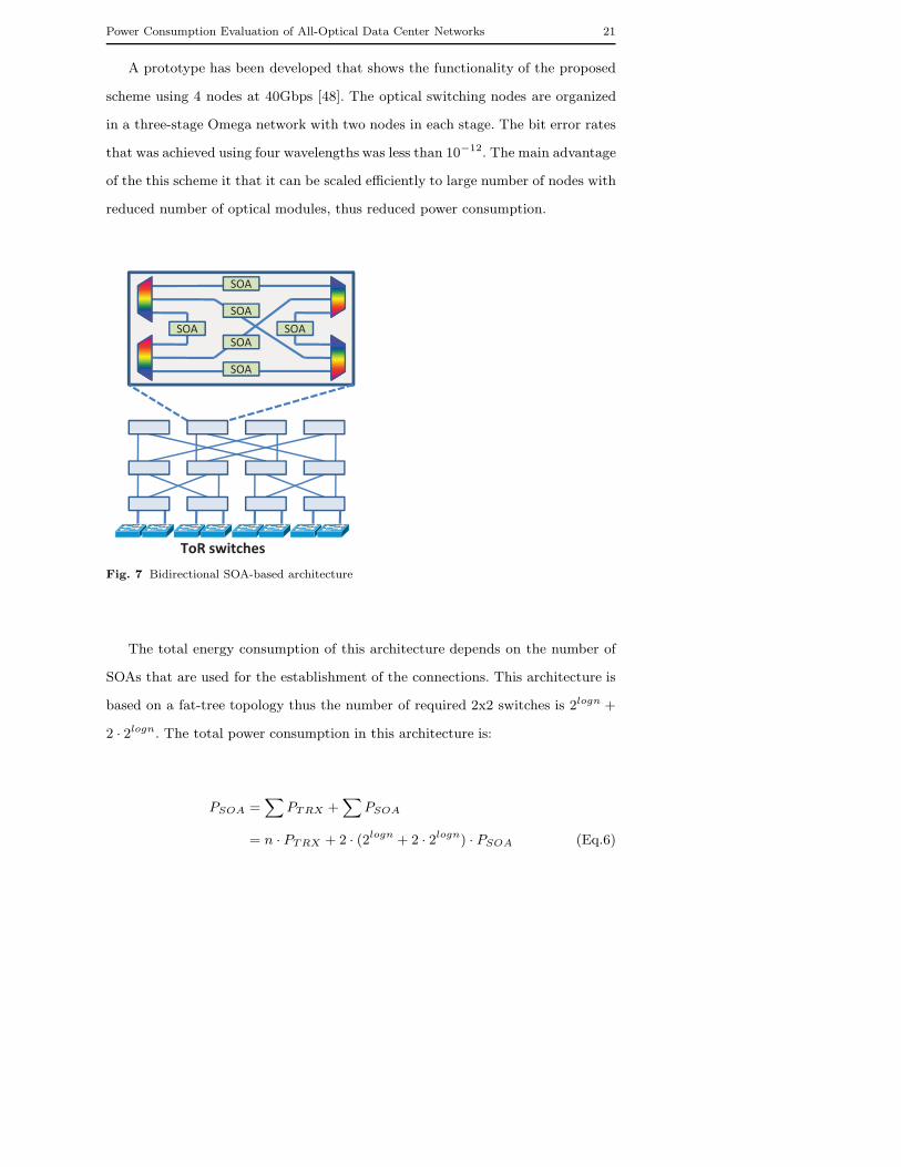
A prototype has been developed that shows the functionality of the proposed
scheme using 4 nodes at 40Gbps [48]. The optical switching nodes are organized
in a three-stage Omega network with two nodes in each stage. The bit error rates
that was achieved using four wavelengths was less than 10−12. The main advantage
of the this scheme it that it can be scaled efficiently to large number of nodes with
reduced number of optical modules, thus reduced power consumption.
SOA
SOASOA
SOA
SOA
SOA SOA
ToR switchesToR switches
Fig. 7 Bidirectional SOA-based architecture
The total energy consumption of this architecture depends on the number of
SOAs that are used for the establishment of the connections. This architecture is
based on a fat-tree topology thus the number of required 2x2 switches is 2logn +
2 · 2logn. The total power consumption in this architecture is:
PSOA =∑
PTRX +∑
PSOA
= n · PTRX + 2 · (2logn + 2 · 2logn) · PSOA (Eq.6)

22 Christoforos Kachris, Ioannis Tomkos
where:
PTRX : Power of the Optical Transceiver
PSOA : Power of the Semiconductor Optical Amplifier
4 Power Consumption Comparison
To evaluate the energy consumption of the optical interconnects, we used the fol-
lowing components shown in Table 1. The most recent 10Gbps SFP+ transceivers
that are used for point-to-point links with multi-mode fibers in current data cen-
ters consume around 1W[5]. Fujitsu has recently presented 40Gbps transceivers
in 65nm CMOS technology consuming only 2.8W targeting the future 40G Eth-
ernet (IEEE802.3ab standard)[14]. The tunable optical transceivers that are used
in AWGR-Clos network consume around 3.5W and can be configured to a wide
range of wavelengths (C-band)[13]. The state-of-the-art SOAs that are readily
available consume around 0.5W while the TWC that consist of a SOA and a tun-
able laser consume around 1.5W[11]. Finally, for the WSS architecture, the power
consumption per port is around 1W which means that each node in the WSS-based
architecture consume 4W [44]. The power consumption per port of the MEMS is
around 1.5W [44]. The power consumption for the DRAM (used for buffering) is
based on a DDR3 DIMM, using 40nm process technology, assuming 60% reads,
and 60% bandwidth [10].
In order to perform a fair and accurate power consumption comparison between
the optical interconnects and the commodity switches we used the power consump-
tion characteristics of the most recent currently available components (both for
the electronic and the optical modules). Projected figures of merit for the power
consumption could be used both for the electronic and the optical components
(such as in [46]). However the predicted values could introduce significant error
in the overall power consumption both for the all-optical architectures and the
architectures using commodity switches. Therefore, to achieve a fair and accurate

Power Consumption Evaluation of All-Optical Data Center Networks 23
Table 1 Power consumption of components
Component Power Consumption(W)
10Gbps Transceiver (SFP+) [5] 1
40Gbps Transceiver [14] 2.8
10Gbps Tunable Transceiver (TXFP) [13] 3.5
SOA [11] 0.5
TWC [22][11] 1.5
WSS (per port, x4 in Rack)[44] 1x4
MEMS (per port)[44] 1.5
SDRAM(1GB,DDR3-60%Rd,60%BW)[10] 0.9
O-E, E-O Converters [22] 2.5
Commodity 32ports 10Gbps switch [8] 300
comparison, this study is performed using only the power consumption character-
istics of the most recent and available optical and electronic components.
Figure 8 depicts the total power consumption of the optical interconnects for
different number of racks. Each rack can host up to 48 blade servers, thus this figure
shows the power consumption of the aggregate network for up to 24,000 servers. For
all architectures we assume 40Gbps optical transceiver at the ToR switch, except
for the WSS-based architecture. The WSS-based scheme is based on an array
of 10Gbps optical transceivers tuned at different wavelength instead of a single
transceiver. As it is shown in the figure, the optical interconnects consume almost
an order of magnitude lower power compared to current data center networks
based on commodity switches. Note that in the current study we only measure the
power consumption of the data plane while we ignore the power consumption of
the control plane (e.g. scheduling). However, the control plane usually consumes
only a small fraction of the total power consumption in the data center networks
[50]. For example, in the case of an IP router using a switch fabric, the control
plane counts only for 10% of the total power consumption (the energy per bit for
the control plane is 1.1nJ while the total energy per bit is 10nJ [42]).
For the reference design based on commodity switches, we assume a 2-Tier
fat-tree topology using aggregate switches of 32 ports at 10Gbps [8]. The reference

24 Christoforos Kachris, Ioannis Tomkos
10000
ption�(W
)AWGR�Buffer
AWGR�Clos�
AWGR Cl TS
100
1000
32 64 128 256 512
Power�con
sum
Number�of�Racks
AWGR�Clos�TS
WSS
B&S
Bidir.�SOA
Reference
300
350
400
450
Fig. 8 Total power consumption comparison
design is similar to the architecture shown in Figure 1. A 2-Tier topology has been
selected that is more widely used and more energy efficient compared to a 3-Tier
topology [7]. The first level consists of the Top-of-Rack (ToR) commodity switches
hosted into the Racks and the second level consists of the aggregate switches that
are also interconnected with each other.
The Broadcast and Select (B&S) architecture consume the lowest power due
to the small number of optical components that are used for each link. In this
case the power consumption of the optical amplifier used in this architecture is set
to 1W. The bidirectional architecture and the AWGR-Buffered architecture con-
sume slightly higher while the AWGR-Clos and the AWGR-Clos-TS architecture
consume almost the same power as both of them are based on a three-stage Clos
network.
Figure 9 depicts the power consumption per Gbps for these optical intercon-
nects compared to the reference design. The power consumption per Gbps is cal-
culated as the maximum power consumption in the case of full interconnection
communication. Note that the reference design utilizes only one 10Gbps links
while the WSS-based scheme utilize an array (32) of 10Gbps transceivers. The
WSS-based and the B&S architectures provide the lowest power consumption per

Power Consumption Evaluation of All-Optical Data Center Networks 25
11
Gbp
s) AWGR�Buffer
AWGR�Clos�
1
Gbp
s�(W
/Gbp
s) AWGR�Buffer
AWGR�Clos�
AWGR�Clos�TS
WSS
B&S
1
ower�per�Gbp
s�(W
/Gbp
s) AWGR�Buffer
AWGR�Clos�
AWGR�Clos�TS
WSS
B&S
Bidir.�SOA
Reference
0.1
1
32 64 128 256 512
Power�per�Gbp
s�(W
/Gbp
s) AWGR�Buffer
AWGR�Clos�
AWGR�Clos�TS
WSS
B&S
Bidir.�SOA
Reference
0.1
1
32 64 128 256 512
Power�per�Gbp
s�(W
/Gbp
s)
Number�of�Racks
AWGR�Buffer
AWGR�Clos�
AWGR�Clos�TS
WSS
B&S
Bidir.�SOA
Reference
0.1
1
32 64 128 256 512
Power�per�Gbp
s�(W
/Gbp
s)
Number�of�Racks
AWGR�Buffer
AWGR�Clos�
AWGR�Clos�TS
WSS
B&S
Bidir.�SOA
Reference
0.16
0.18
0.12
0.14
Fig. 9 Power consumption per Gbps
Gbps (both of them around 0.11W/Gbps), while the AWGR-Buffered (e.g. DOS)
and the Bidirectional-SOA-based consume slightly higher. However, note that in
the WSS-based and the AWGR-Buffered the packet delay is not constant as in the
other schemes. In the case of AWGR-Buffered the packets may experience delay
in the SDRAM buffer, while in the case of WSS scheme the packets may traverse
several nodes due to a lack of a direct connection between two nodes. Thus in these
schemes, the energy consumption per Gb will be slightly higher than the power
consumption per Gbps (in all the other schemes the delay of the packet is constant
thus the energy consumption per Gb is proportional to the power consumption per
Gbps). But as it is shown in this figure the most important fact is that all of the
optical interconnects consume almost an order of magnitude lower power than the
commodity switches. Even if the control plane would contribute additional 10-20%
of the total power consumption, the optical architectures would still provide sig-
nificantly higher energy efficiency than the reference design. Another advantage of
these optical interconnects is that they are bandwidth agnostic. Therefore, these
architectures can be scaled efficiently using higher bandwidth optical transceivers
(e.g. 40Gbps or 100Gbps in the future) without any changes in the architecture

26 Christoforos Kachris, Ioannis Tomkos
since the switching is performed at the optical domain. Thus, optical interconnects
seem as a promising solution for the future data center networks providing high
throughput, reduced latency and significantly lower power consumption.
Table 2 shows the difference characteristics of each architecture in terms of
switching or reconfiguration time, capacity limitation and scalability. The WSS-
based architecture is the only one that is based on optical MEMS switches that
have high reconfiguration time (in the order of few ms). All the other architectures
are based on tunable wavelength converters [36] or SOAs [20] that can achieve very
low switching times (in the order of a few ns). However theWSS-based architecture
achieves all-to-all communication using several hops. Therefore the reconfiguration
is only required when the bulky and long lived connection have changed which
usually happens every few ms [30].
The table also shows the scalability of each architecture. Optical networks
need to scale easily to a large number of nodes (e.g. ToR switches) especially
in warehouse-scale data centers. The WSS-based architecture, the AWGR-buffer
and the B&S architecture are implemented through a central switch that can
accommodate limited number of nodes (usually constrained by the number of
wavelength channels). However, when the AWGR-based architecture is connected
in a Clos topology (AWGR-clos and AWGR-Clos-TS) it can support a high number
of nodes. Similarly the Bidirectional SOA, due to its topology, can be easily scaled
to high number of nodes using the 2x2 switching nodes in a banyan network.
Besides the scalability in terms of number of nodes the proposed schemes must
be also easy to upgrade to higher capacities per node. TheWSS-based architectures
that is based on WSS and MEMS switches can be easily upgrade to 40 Gbps, 100
Gbps or higher bit rates since the WSS and the MEMS switches can support
any data rate (data rate agnostic). Therefore, in these architectures the maximum
capacity per node is determined only by the data rate of the optical transceivers.
On the other hand the AWGR-based architectures are based on tunable wave-
length converters for the switching. Therefore the maximum capacity per node
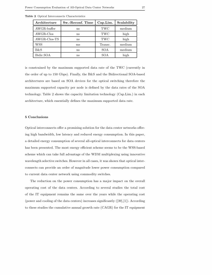
Power Consumption Evaluation of All-Optical Data Center Networks 27
Table 2 Optical Interconnects Characteristics
Architecture Sw.-Reconf. Time Cap.Lim. Scalability
AWGR-buffer ns TWC medium
AWGR-Clos ns TWC high
AWGR-Clos-TS ns TWC high
WSS ms Transc. medium
B&S ns SOA medium
Bidir.SOA ns SOA high
is constrained by the maximum supported data rate of the TWC (currently in
the order of up to 150 Gbps). Finally, the B&S and the Bidirectional SOA-based
architectures are based on SOA devices for the optical switching therefore the
maximum supported capacity per node is defined by the data rates of the SOA
technology. Table 2 shows the capacity limitation technology (Cap.Lim.) in each
architecture, which essentially defines the maximum supported data rate.
5 Conclusions
Optical interconnects offer a promising solution for the data center networks offer-
ing high bandwidth, low latency and reduced energy consumption. In this paper,
a detailed energy consumption of several all-optical interconnects for data centers
has been presented. The most energy efficient scheme seems to be the WSS-based
scheme which can take full advantage of the WDM multiplexing using innovative
wavelength selective switches. However in all cases, it was shown that optical inter-
connects can provide an order of magnitude lower power consumption compared
to current data center network using commodity switches.
The reduction on the power consumption has a major impact on the overall
operating cost of the data centers. According to several studies the total cost
of the IT equipment remains the same over the years while the operating cost
(power and cooling of the data centers) increases significantly ([39],[1]). According
to these studies the cumulative annual growth rate (CAGR) for the IT equipment

28 Christoforos Kachris, Ioannis Tomkos
was only 2.7% while the CAGR for the power and cooling was 11.2% during the
period 2005-2010. In 2005 the electricity bill was only half of the total operation
cost while in the near future it will be almost the same as the IT cost.
The cost of optical interconnects depends mainly on the type and the maturity
of the optical components. The architectures that are based on commercially avail-
able optical components (e.g. WSS and MEMS) can be adopted easily and have
relatively low cost. On the other hand, the architectures that are based on novel
and specialized optical modules such as the broadcast and select architecture may
have increased cost due to the high Non-Recurring Engineering (NRE) cost.
In any case, even if the cost of the optical interconnects is higher than the
commodity switches, this cost can be compensated by the lower operating cost
due to reduced power consumption. The reduction of the power consumption re-
sults to significantly reduced electricity expenses thus enabling a short period for
the Return-of-Investment (ROI). A study has shown that if the cost of the optical
interconnects is the same as the current switches, the ROI can be achieved in 5
years time frame even if the optical interconnects consume 80% of the commodity
switches [29]. On the other hand, if the optical interconnect cost twice the price
of the current switches then it must consume less than 50% of the current power
consumption to achieve the ROI in 5 years time frame. Therefore, optical inter-
connects can be a promising alternative that can meet the bandwidth and power
consumption requirements of the future data center networks while also providing
lower operation cost.
References
1. The Impact of Power and Cooling on Data Center Infrastructure. Market Analysis, IDC
Inc. (2007)
2. Report to Congress on Server and Data Center Energy Efficiency. U.S. Environmental
Protection Agency, ENERGY STAR Program (2007)
3. Wavelength Selective Switches for ROADM applications. Datasheet, Finisar Inc. (2008)

Power Consumption Evaluation of All-Optical Data Center Networks 29
4. Where does power go? GreenDataProject, available online at:
http://www.greendataproject.org (2008)
5. Cisco 10GBASE SFP+ Modules. Datasheet, Cisco Inc. (2010)
6. Cisco Catalyst 2560 Switch. Datasheet, Cisco Inc. (2010)
7. Cisco Data Center Interconnect Design and Deployment Guide. Cisco Press (2010)
8. Cisco Nexus 5548P Switch. Datasheet, Cisco Inc. (2010)
9. Make IT Green, Cloud Computing and its Contribution to Climate Change. Greenpeace,
March 2010 (2010)
10. Samsung Green DDR3. Datasheet, Samsung Inc. (2010)
11. SOA-S-C-14-FCS 1.55um Semiconductor Optical Amplifier. Datasheet, CIP Technologies
Inc. (2010)
12. The 50G Silicon Photonics Link. Intel Labs, White Paper, Intel Inc. (2010)
13. Tunable Multiprotocol XFP Optical Transceiver - 1550nm, JXP Series. Datasheet, JDSU
Inc. (2010)
14. Amamiya, Y., Kaeriyama, S., Noguchi, H., Yamazaki, Z., Yamase, T., Hosoya, K.,
Okamoto, M., Tomari, S., Yamaguchi, H., Shoda, H.: A 40Gb/s multi-data-rate CMOS
transceiver chipset with SFI-5 interface for optical transmission systems. In: IEEE Inter-
national Solid-State Circuits Conference, pp. 358–359 (2009)
15. Barker, K.J., Benner, A.F., Hoare, R.R., Hoisie, A., Jones, A.K., Kerbyson, D.J., Li,
D., Melhem, R.G., Rajamony, R., Schenfeld, E., Shao, S., Stunkel, C.B., Walker, P.: On
the feasibility of optical circuit switching for high performance computing systems. In:
Supercomputing Conference. DOI 10.1145/1105760.1105781
16. Benson, T., Akella, A., Maltz, D.A.: Network traffic characteristics of
data centers in the wild. In: Proceedings of the 10th annual confer-
ence on Internet measurement, IMC ’10, pp. 267–280. ACM, New York,
NY, USA (2010). DOI http://doi.acm.org/10.1145/1879141.1879175. URL
http://doi.acm.org/10.1145/1879141.1879175
17. Benson, T., Anand, A., Akella, A., Zhang, M.: Understanding data center
traffic characteristics. In: Proceedings of the 1st ACM workshop on Re-
search on enterprise networking, WREN ’09, pp. 65–72. ACM, New York,
NY, USA (2009). DOI http://doi.acm.org/10.1145/1592681.1592692. URL
http://doi.acm.org/10.1145/1592681.1592692
18. Davis, A.: Photonics and Future Datacenter Networks. In: HOT Chips, A Symposium on
High Performance Chips, Stanford (2010)
19. Dean, J., Ghemawat, S.: MapReduce: simplified data processing on large clusters. Com-
mun. ACM 51, 107–113 (2008)
30 Christoforos Kachris, Ioannis Tomkos
20. Eramo, V., Listanti, M.: Power consumption in bufferless optical packet switches in soa
technology. J. Opt. Commun. Netw. 1(3), B15–B29 (2009)
21. Farrington, N., Porter, G., Radhakrishnan, S., Bazzaz, H.H., Subramanya, V., Fainman,
Y., Papen, G., Vahdat, A.: Helios: a hybrid electrical/optical switch architecture for mod-
ular data centers. In: Proceedings of the ACM SIGCOMM 2010 conference on SIGCOMM,
SIGCOMM ’10, pp. 339–350 (2010)
22. Fujioka, N., Chu, T., Ishizaka, M.: Compact and low power consumption hybrid integrated
wavelength tunable laser module using silicon waveguide resonators. J. Lightwave Technol.
28(21), 3115–3120 (2010)
23. Glick, M.: Optical interconnects in next generation data centers: An end to end view. In:
Proceedings of the 2008 16th IEEE Symposium on High Performance Interconnects, pp.
178–181 (2008)
24. Gripp, J., Simsarian, J.E., LeGrange, J.D., Bernasconi, P., Neilson, D.T.: Photonic terabit
routers: The iris project. In: Optical Fiber Communication Conference, p. OThP3. Optical
Society of America (2010)
25. Hemenway, R., Grzybowski, R., Minkenberg, C., Luijten, R.: Optical-packet-switched in-
terconnect for supercomputer applications. J. Opt. Netw. 3(12), 900–913 (2004)
26. Hida, Y., Hibino, Y., Kitoh, T., Inoue, Y., Itoh, M., Shibata, T., Sugita, A., Himeno, A.:
400-channel 25-GHz spacing arrayed-waveguide grating covering a full range of C- and
L-bands. In: Optical Fiber Communication Conference and Exhibit (2001)
27. Hlavacs, H., Da Costa, G., Pierson, J.M.: Energy consumption of residential and profes-
sional switches. In: Proceedings of the 2009 International Conference on Computational
Science and Engineering - Volume 01, CSE ’09, pp. 240–246 (2009)
28. Hoelzle, U., Barroso, L.A.: The Datacenter as a Computer: An Introduction to the Design
of Warehouse-Scale Machines, 1st edn. Morgan and Claypool Publishers (2009)
29. Kachris, C., Tomkos, I.: A Survey on Optical Interconnects for Data
Centers. IEEE Communications Surveys and Tutorials (2011). DOI
http://doi:10.1109/SURV.2011.122111.00069
30. Kandula, S., Sengupta, S., Greenberg, A., Patel, P., Chaiken, R.: The nature of
data center traffic: measurements & analysis. In: Proceedings of the 9th ACM SIG-
COMM conference on Internet measurement conference, IMC ’09, pp. 202–208. ACM,
New York, NY, USA (2009). DOI http://doi.acm.org/10.1145/1644893.1644918. URL
http://doi.acm.org/10.1145/1644893.1644918
31. Lam, C.F., Liu, H., Koley, B., Zhao, X., Kamalov, V., Gill, V.: Fiber optic communication
technologies: what’s needed for datacenter network operations. Communications Magazine
48, 32–39 (2010)
32. Lee, D.: Scaling Networks in Large Data Centers. OFC/NFOEC, Invited Talk (2011)

Power Consumption Evaluation of All-Optical Data Center Networks 31
33. Luijten, R., Denzel, W.E., Grzybowski, R.R., Hemenway, R.: Optical interconnection net-
works: The OSMOSIS project. In: The 17th Annual Meeting of the IEEE Lasers and
Electro-Optics Society (2004)
34. Minkenberg, C.: The rise of the interconnects. In: HiPEAC Interconnects cluster
meeting, Barcelona (2010). DOI http://doi.acm.org/10.1145/1868447.1868455. URL
http://www.hipeac.net/Interconnects
35. Papadimitriou, G.I., Papazoglou, C., Pomportsis), A.S.: Optical switching: Switch fabrics,
techniques, and architectures. Journal of Lightwave Technology 21(2), 384 (2003)
36. Pina, J.F., da Silva, H.J.A., Monteiro, P.N., Wang, J., Freude, W., Leuthold, J.: Perfor-
mance Evaluation of Wavelength Conversion at 160 Gbit/s using XGM in Quantum-Dot
Semiconductor Optical Amplifiers in MZI configuration. In: Photonics in Switching (2007)
37. Proietti, R., Ye, X., Yin, Y., Potter, A., Yu, R., Kurumida, J., Akella, V., Yoo, S.J.B.: 40
Gb/s 88 Low-latency Optical Switch for Data Centers (2011)
38. Ramaswami, R., Sivarajan, K., Sasaki, G.: Optical Networks: A Practical Perspective, 3rd
Edition, 3rd edn. Morgan Kaufmann Publishers Inc., San Francisco, CA, USA (2009)
39. Scaramell, J.: Worldwide Server Power and Cooling Expense. 2006-2010 Forecast, Market
analysis, IDC Inc.
40. Schulz, G.: The Green and Virtual Data Center, 1st edn. Auerbach Publications, Boston,
MA, USA (2009)
41. Shacham, A., Bergman, K.: An experimental validation of a wavelength-striped, packet
switched, optical interconnection network. J. Lightwave Technol. 27(7), 841–850 (2009)
42. Shen, G., Tucker, R.S.: Energy-Minimized Design for IP Over WDM Networks. Optical
Communication and Networking pp. 176–186 (2009)
43. Simsarian, J., Larson, M., Garrett, H., Hu, H., Strand, T.: Less than 5-ns wavelength
switching with an SG-DBR laser. Photonics Technology Letters 18, 565–567 (2006)
44. Singla, A., Singh, A., Ramachandran, K., Xu, L., Zhang, Y.: Proteus: a topology malleable
data center network. In: Proceedings of the Ninth ACM SIGCOMM Workshop on Hot
Topics in Networks, Hotnets ’10, pp. 8:1–8:6 (2010)
45. Singla, A., Singh, A., Ramachandran, K., Xu, L., Zhang, Y.: Feasibility Study on Topol-
ogy Malleable Data Center Networks (DCN) Using Optical Switching Technologies. In:
Proceedings of the Optical Fiber Communication Conference and Exposition (OFC) and
the National Fiber Optic Engineers Conference (NFOEC) (2011)
46. Tucker, R.: Green Optical CommunicationsPart II: Energy Limitations in Networks. IEEE
Journal of Selected Topics in Quantum Electronics 17(2), 261–274 (2011)
47. Wang, G., Andersen, D.G., Kaminsky, M., Papagiannaki, K., Ng, T.E., Kozuch, M., Ryan,
M.: c-Through: Part-time Optics in Data Centers. In: Proceedings of the ACM SIGCOMM
2010 conference on SIGCOMM, SIGCOMM ’10, pp. 327–338 (2010)

32 Christoforos Kachris, Ioannis Tomkos
48. Wang, H., Bergman, K.: A Bidirectional 2x2 Photonic Network Building-Block for High-
Performance Data Centers. In: Optical Fiber Communication Conference. Optical Society
of America (2011)
49. Xia, K., Kaob, Y.H., Yangb, M., Chao, H.J.: Petabit Optical Switch for Data Center
Networks. In: Technical report, Polytechnic Institute of New York University, available
at: http://eeweb.poly.edu/chao/publications/petasw.pdf (2010)
50. Ye, T.T., Benini, L., Micheli, G.D.: Analysis of power consumption on switch fabrics in
network routers. In: In Proc. Design Automation Conference, pp. 524–529 (2002)
51. Ye, X., Yin, Y., Yoo, S.J.B., Mejia, P., Proietti, R., Akella, V.: DOS: a scalable optical
switch for datacenters. In: Proceedings of the 6th ACM/IEEE Symposium on Architectures
for Networking and Communications Systems, ANCS ’10, pp. 24:1–24:12 (2010)
Related Documents