1 Polymorphism in Post-Dichalcogenide Two- Dimensional Materials Hadallia Bergeron, 1 Dmitry Lebedev, 1 and Mark C. Hersam 1,2,3,* 1 Department of Materials Science and Engineering, Northwestern University, Evanston Illinois 60208, United States 2 Department of Chemistry, Northwestern University, Evanston Illinois 60208, United States 3 Department of Electrical and Computer Engineering, Northwestern University, Evanston Illinois 60208, United States *Corresponding author: [email protected] Abstract Two-dimensional (2D) materials exhibit a wide range of atomic structures, compositions, and associated versatility of properties. Furthermore, for a given composition, a variety of different crystal structures (i.e., polymorphs) can be observed. Polymorphism in 2D materials presents a fertile landscape for designing novel architectures and imparting new functionalities. The objective of this Review is to identify the polymorphs of emerging 2D materials, describe their polymorph- dependent properties, and outline methods used for polymorph control. Since traditional 2D materials (e.g., graphene, hexagonal boron nitride, and transition metal dichalcogenides) have already been studied extensively, the focus here is on polymorphism in post-dichalcogenide 2D materials including group III, IV, and V elemental 2D materials, layered group III, IV, and V metal chalcogenides, and 2D transition metal halides. In addition to providing a comprehensive survey of recent experimental and theoretical literature, this Review identifies the most promising

Welcome message from author
This document is posted to help you gain knowledge. Please leave a comment to let me know what you think about it! Share it to your friends and learn new things together.
Transcript
1
Polymorphism in Post-Dichalcogenide Two-
Dimensional Materials
Hadallia Bergeron,1 Dmitry Lebedev,1 and Mark C. Hersam1,2,3,*
1Department of Materials Science and Engineering, Northwestern University, Evanston Illinois
60208, United States
2Department of Chemistry, Northwestern University, Evanston Illinois 60208, United States
3Department of Electrical and Computer Engineering, Northwestern University, Evanston Illinois
60208, United States
*Corresponding author: [email protected]
Abstract
Two-dimensional (2D) materials exhibit a wide range of atomic structures, compositions,
and associated versatility of properties. Furthermore, for a given composition, a variety of different
crystal structures (i.e., polymorphs) can be observed. Polymorphism in 2D materials presents a
fertile landscape for designing novel architectures and imparting new functionalities. The objective
of this Review is to identify the polymorphs of emerging 2D materials, describe their polymorph-
dependent properties, and outline methods used for polymorph control. Since traditional 2D
materials (e.g., graphene, hexagonal boron nitride, and transition metal dichalcogenides) have
already been studied extensively, the focus here is on polymorphism in post-dichalcogenide 2D
materials including group III, IV, and V elemental 2D materials, layered group III, IV, and V metal
chalcogenides, and 2D transition metal halides. In addition to providing a comprehensive survey
of recent experimental and theoretical literature, this Review identifies the most promising
2
opportunities for future research including how 2D polymorph engineering can provide a pathway
to materials by design.
Table of Contents
1. Introduction ........................................................................................................................... 4
1.1. Polymorphism ...................................................................................................................... 4
1.2. Polymorphism in Post-Dichalcogenide 2D Materials .......................................................... 6
1.3. Experimental Distinction of 2D Polymorphs ....................................................................... 8
1.4. Nomenclature ....................................................................................................................... 9
2. Elemental 2D Materials ...................................................................................................... 11
2.1. Group III Elements ............................................................................................................ 11
2.1.1. Structures and properties of 2D boron polymorphs .................................................... 11
2.1.2. Polymorph control of 2D boron .................................................................................. 14
2.1.2.1. Substrates. ............................................................................................................ 14
2.1.2.2. Synthesis conditions............................................................................................. 16
2.1.2.3. Post-synthesis processing .................................................................................... 17
2.2. Group IV Elements ............................................................................................................ 18
2.2.1. Structures and properties of 2D group IV elemental polymorphs .............................. 18
2.2.2. Polymorph control of 2D group IV elemental materials ............................................ 22
2.2.2.1. Substrates. ............................................................................................................ 22
2.2.2.2. Synthesis conditions............................................................................................. 26
2.2.2.3. Post-synthesis processing. ................................................................................... 28
2.3. Group V Elements.............................................................................................................. 29
2.3.1. Structures and properties of 2D group V elemental polymorphs ............................... 29
2.3.2. Polymorph control of 2D group V elemental materials .............................................. 36
2.3.2.1. Synthesis conditions............................................................................................. 36
2.3.2.2. Substrates. ............................................................................................................ 37
2.3.2.3. Thickness. ............................................................................................................ 40
2.3.2.4. Post-synthesis processing .................................................................................... 41
3. Post-Transition Metal Chalcogenides ............................................................................... 43
3.1. Group III Metal Chalcogenides ......................................................................................... 43
3.1.1. Structures and properties of 2D group III metal chalcogenide polymorphs ............... 43
3
3.1.1.1. MIIIX compounds. ................................................................................................ 44
3.1.1.2. In2Se3 .................................................................................................................... 46
3.1.2. Polymorph control of 2D group III metal chalcogenides ........................................... 51
3.1.2.1. Synthesis conditions............................................................................................. 51
3.1.2.2. Substrates. ............................................................................................................ 52
3.1.2.3. Post-synthesis processing. ................................................................................... 53
3.1.2.3. Thickness ............................................................................................................. 55
3.2. Group IV Metal Chalcogenides ......................................................................................... 58
3.2.1. Structures and properties of 2D group IV metal chalcogenide polymorphs ............... 58
3.2.1.1. MX compounds .................................................................................................... 58
3.2.1.2. MIVX2 compounds ................................................................................................ 61
3.2.2. Polymorph control of 2D group IV metal chalcogenides ........................................... 66
3.2.2.1. Synthesis conditions............................................................................................. 66
3.2.2.2. Substrates ............................................................................................................. 68
3.2.2.3. Post-synthesis processing .................................................................................... 69
3.2.2.3. Thickness. ............................................................................................................ 70
3.3. Group V Metal Chalcogenides ............................................................................................... 72
3.3.1. Structures and properties of 2D group V metal chalcogenide polymorphs ................ 72
3.3.1.1. MV2X3 compounds. ............................................................................................... 72
3.3.2.1. (MV2)m(MV
2X3)n compounds. ................................................................................ 75
3.3.2. Polymorph control of 2D group V metal chalcogenides ............................................ 82
3.3.2.1. Growth. ................................................................................................................ 82
3.3.2.1. Pressure and Temperature. ................................................................................... 82
4. Layered Transition Metal Halides .................................................................................... 84
4.1. Transition Metal Dihalides ................................................................................................ 87
4.1.1. Structures and properties of 2D transition metal dihalide polymorphs ...................... 87
4.1.2. Polymorph control of 2D transition metal dihalides ................................................... 92
4.2. Transition Metal Trihalides ................................................................................................ 93
4.2.1. Structures and properties of 2D transition metal trihalide polymorphs ...................... 93
4.2.1.1. Vanadium triiodide. ............................................................................................. 94
4.2.1.2. Chromium trihalides. ........................................................................................... 96
4.2.1.3. Ruthenium trichloride. ......................................................................................... 98
4.2.1.4. Other MY3 halides. ............................................................................................. 100
4.2.2. Polymorph control of 2D transition metal trihalides ................................................ 106
4
4.3. Transition Metal Halides of Other Stoichiometries ......................................................... 110
5. Conclusions and Outlook ................................................................................................. 111
5.1. Discovery of 2D Polymorphs ........................................................................................... 113
5.2. Stabilization of 2D Polymorphs ....................................................................................... 114
5.3. Polymorph Engineering and Functionality ...................................................................... 116
6. Author Information .......................................................................................................... 121
6.1. Biographies ...................................................................................................................... 121
7. Acknowledgements ........................................................................................................... 122
8. References .......................................................................................................................... 122
1. Introduction
1.1. Polymorphism
Polymorphism is a fundamental principle of nature and a widespread phenomenon affecting
various scientific disciplines. In the context of crystallography, polymorphism is the “occurrence
of different crystal structures for the same chemical entity.”1 Herein, the “chemical entity” can
include small variances in chemical composition to account for non-stoichiometric defective or
doped compounds. Readers may also be familiar with polymorphism from the field of genetics,
where it refers to variants in a particular DNA sequence,2 or in organic chemistry, where it
describes supramolecular isomerism, which has been the subject of concentrated research efforts
in pharmacology.3–5 Whereas in the aforementioned fields the importance of polymorph
engineering is well-established, this concept is still incipient for two-dimensional (2D) materials.
However, 2D materials exhibit rich polymorphism that has profound implications for higher-order
materials engineering in the atomically thin limit. Polymorphism is at the root of crystal
engineering and the materials science paradigm – i.e., to control structure is to control properties.
5
Therefore, polymorph engineering offers a unique pathway to the grand challenge of rational
design of 2D materials with predefined architectures and functionalities.
The manifestation of polymorphism presents both a challenge and an opportunity. For
instance, competing polymorphs can make the synthesis of pure phases difficult as is the case for
several 2D materials discussed here (e.g., borophene and indium selenide), where single-phase
synthesis has not yet been mastered. On the other hand, polymorphism provides opportunities for
additional structure and property control beyond chemical composition, thus enabling the
discovery and engineering of novel 2D polymorphs. Similar to bulk materials, various processing
conditions exert structural control over 2D polymorphic materials including temperature, pressure,
and related environmental variables. However, the 2D regime also offers additional environmental
variables to influence the occurrence of polymorphs, particularly the dominance of surface effects
(e.g., the influence of thickness or substrates) in the 2D limit. Consequently, structures that are not
observed in the bulk can be stabilized in the 2D regime, which implies fundamentally different
opportunities for polymorph engineering in atomically thin materials.
Polymorphism encompasses several different categories of structural variation. The most
intuitive notion of polymorphism is when a single composition can form different crystal structures
of entirely different symmetry and periodicity. The archetypal example of this is bulk elemental
carbon, which can take the form of graphite (space group P63/mmc, lattice constants a = 2.46 Å
and c = 6.71 Å) and diamond (space group Fd3m, a = 3.56 Å) among others.6 The various
structures of carbon are also referred to as “allotropes,” a term used to describe polymorphs of
elemental materials.1 More subtle forms of polymorphism also exist such as polytypism.
Polytypism applies to close-packed or layered materials, where polytypes are characterized by
constituent layers with identical structures but different periodicities perpendicular to the layer
6
plane (i.e., different stacking).7 Since van der Waals (vdW) layered materials have weak interlayer
interactions, polytypism is a commonly observed and highly relevant form of polymorphism for
multilayer 2D materials. Taking the example of graphite, the hexagonal (2H) polytype with a
bilayer unit cell accounts for most naturally occurring crystals, but a higher-energy rhombohedral
modification with a trilayer unit cell can be obtained via mechanical grinding.8 For 2D materials,
this concept can be taken further to artificial polytypes, as was recently demonstrated in twisted
bilayer graphene. By stacking two graphene layers with a small twist angle (magic angle of ~1.1
o), a moiré pattern appears that results in the formation of flat bands9,10 and unique correlated
electronic states,11,12 including superconductivity.13,14 The aforementioned examples of carbon
polymorphism are instances where the various forms can coexist over a range of experimental
conditions. In contrast, some polymorphs are effectively exclusive to different environmental
conditions. For example, sp2-coordinated glassy carbon can be compressed into an amorphous
high-pressure sp3-coordinated allotrope, but unlike diamond, it rapidly recovers its original sp2
coordination upon return to ambient conditions.15
Implicit in the discussion of polymorphism is the concept of (meta)stability. It is possible
to observe higher-energy metastable structures other than the ground state structure(s) under the
right conditions. The energetic discrepancies between polymorphs can range from effectively
degenerate to barely experimentally feasible, but compounds recognized as being concomitantly
polymorphic generally exhibit structures with similar lattice energies. In addition, kinetic
influences are also crucial to the observation of polymorphs. Kinetics often dictate whether
polymorphs are observed to coexist or are exclusive, and whether individual structures are
effectively stable (i.e., long-lived metastable state) or transiently observed.
1.2. Polymorphism in Post-Dichalcogenide 2D Materials
7
This Review explores the identity and control of 2D polymorphs in the recent post-dichalcogenide
2D literature – namely, recently emerging 2D materials following the advent of the transition metal
dichalcogenides (TMDs) such as MoS2, WS2, MoSe2, WSe2, and MoTe2. TMDs also exhibit
polymorphism with their structures and phase engineering already having been detailed in previous
reviews.16–22 In contrast, the focus of this Review is 2D polymorphism in group III, IV, and V
elemental materials, layered group III, IV, and V metal chalcogenides, and vdW transition metal
halides (TMHs). For each class of materials, the emphasis is placed on polymorphs that are 2D or
vdW-layered in nature, rather than non-layered three-dimensional (3D) structures. The covered 2D
materials exhibit a wide range of polymorphic variations including entirely different monolayer
structures, multilayer stacking polytypes, as well as polymorphs that coexist under the same
conditions or are mutually exclusive. Furthermore, 2D materials also demonstrate substrate-
induced monolayer reconstructions such that many monolayer materials have calculated ground
state freestanding forms that are altered when interacting with a substrate, resulting in novel
polymorphs in the ultrathin limit. The increased contribution of surface energy in 2D materials
also enables thickness-induced structural transformations. In addition to substrate and thickness
effects, more conventional means of polymorph control such as manipulation of synthesis
conditions (e.g., temperature and pressure) or post-synthesis processing (e.g., thermal annealing)
will be discussed. We do not discuss 2D structural variations arising from complex ground states
or other complex physical phenomena (e.g., charge density wave formation or superconductivity),
even though the formation of such a ground state may result in commensurate or incommensurate
lattice distortions that could fall under the definition of polymorphism. Currently, the 2D materials
literature generally does not refer to these phases as polymorphs and instead treats them from a
physical perspective.20,23–25
8
For each material class, the 2D structures and polymorph-dependent properties are
presented, followed by a discussion of methods for achieving polymorph control. The Review
includes both experimental and theoretical work, which are interwoven throughout. The Review
concludes with a discussion on outstanding challenges and opportunities in polymorph engineering
for 2D materials by design.
1.3. Experimental Distinction of 2D Polymorphs
Resolving the structure of 2D polymorphs often presents its own challenge. In particular, X-ray
diffraction (XRD), which is commonly employed for bulk crystals, has limited applicability to the
ultrathin and platelet nature of 2D films or individual exfoliated crystals, reducing both the number
and intensity of Bragg peaks for indexing. Polytypes tend to be particularly difficult to distinguish
using diffraction experiments since they often show similarities in overall symmetry in addition to
identical intralayer structures. Since the occurrence of stacking faults is also associated with
polytypic crystals, it is important to reliably differentiate between polymorphs and local defects.
Techniques that have proven to be particularly beneficial in clarifying the polymorphs of 2D
materials include grazing incidence XRD, scanning tunneling microscopy (STM), selected area
electron diffraction (SAED), and transmission electronic microscopy (TEM), especially high-
angle annular dark-field (HAADF) scanning TEM (STEM). These techniques are especially
powerful when paired with other methods that provide complementary information, such as Raman
spectroscopy and second harmonic generation (SHG). Furthermore, many 2D materials are
currently limited to synthesis and characterization in ultrahigh vacuum conditions, such that the
elucidation of their structures is almost exclusively reliant on STM. In these cases, carbon
monoxide (CO)-functionalized atomic force microscopy has been a powerful tool in interpreting
the observed 2D structures.

9
1.4. Nomenclature
The nomenclature used to denote polymorphs of an element or compound is not uniformly
standardized, which can lead to confusion. As Herbstein aptly puts it, the research community
generally treats “well-intentioned suggestions with disdain, leaving its practitioners to sort out the
confusion for themselves.”1 The nomenclature for 2D polymorphs is no exception. To minimize
ambiguity, this Review uses descriptive nomenclature that invokes the structure discussed, in
addition to providing the space group for each polymorph. This nomenclature breaks down into
two main approaches: (1) the use of structural prototypes as reference points (e.g., “CdI2-type”),
(2) the use of descriptive names such as “hexagonal buckled” (hb) or “asymmetric washboard”
(aw). This practice helps identify common structures among 2D materials. For example, this
nomenclature makes clear that the group V elements and group IV metal chalcogenides both
exhibit similar structures (hb and aw, specifically), which might not be apparent under different
conventions. Furthermore, the naming and recognition of polymorphs is highly dependent upon
literature precedent, so alternate names for single polymorphs that appear in the literature are
provided whenever possible. In particular, other common naming schemes utilize colors,
Strukturbericht designation, or lowercase Greek letters (which are usually given alphabetically in
order of discovery, stability, or temperature). For instance, the most stable structure of arsenic can
be described as grey arsenic, A7-arsenic, or α-arsenic. In this Review, the structure will be referred
to as hb-arsenic since it is composed of layers of hexagonal buckled atoms. Despite this effort at
consistency in nomenclature, some minor exceptions will be employed: (1) notations for overlayer
structures are given as the overlayer unit cell periodicity with respect to the substrate unit cell (n
× m), and (2) vacancy-concentration-based nomenclature is used for borophene and will be
introduced in the corresponding section.
10
Polytypes also have their own nomenclature. Here, Ramsdell notation26 is used in addition
to ABC notation. The former takes the form nZ, where n is given by the number of vdW layers in
a unit cell and Z is given by the crystal and lattice systems of the structure: H indicates a hexagonal
crystal and lattice systems, T indicates a trigonal crystal system with a hexagonal Bravais lattice,
and R indicates a trigonal crystal system with a rhombohedral Bravais lattice.27 Additionally,
subscripts can be used in Ramsdell notation to denote different stacking orders of the same unit
cell size and symmetry (e.g., 2Ha, 2Hb).7,28 In this Review, the Ramsdell notation is used with
respect to the vdW layers of a material (i.e., the ensemble of strongly bonded atomic sheets
separated by vdW gaps), in contrast to some literature that refers to the individual atomic layers
within a vdW layer.29 Additionally, ABC notation is employed to denote the relationship between
vdW layers in the unit cell of a polytype. Using graphite as an example, the most common polytype
is known as 2H-graphite, where two atomic layers of carbon are stacked in a translationally offset
AB sequence to form a unit cell of a hexagonal lattice. Furthermore, the expanded “AbACaC”
notation is used to detail the relative position of cations (usually lowercase letter) and anions
(usually uppercase letter) in different vdW layers. This notation is commonly used for TMDs. For
example, AbACaC stacking implies that the unit cell consists of two layers in the out-of-plane
direction, namely an AbA and a CaC layer separated by a vdW gap. The layers are shifted or
rotated such that cations in the latter layer (a) are located on top of anions in the former layer (A).
Therefore, AbACaC stacking indicates three distinct columns of atoms in the out-of-plane
direction, whereas an AbABaB stacking pattern would only have two.
Lastly, while the terms “dimorphs” or “trimorphs” are sometimes used to denote the
occurrence of two or three polymorphic forms of a compound, respectively, this Review foregoes
this specification and instead uses the general term “polymorphs” to denote any number of

11
polymorphic variations. This terminology is more accommodating to the future discovery of
additional structures for a given compound.
2. Elemental 2D Materials
2.1. Group III Elements
With the synthesis of 2D boron (i.e., ‘borophene’) in 2015,30,31 the 2D material family expanded
to include group III elements. Beyond boron, potential structures and synthesis conditions have
been investigated for other 2D group III elements such as Al,32,33 Ga,34 and In,35 but the literature
is quite limited. Consequently, borophene currently represent the most reliably synthesized
monolayer group III element.
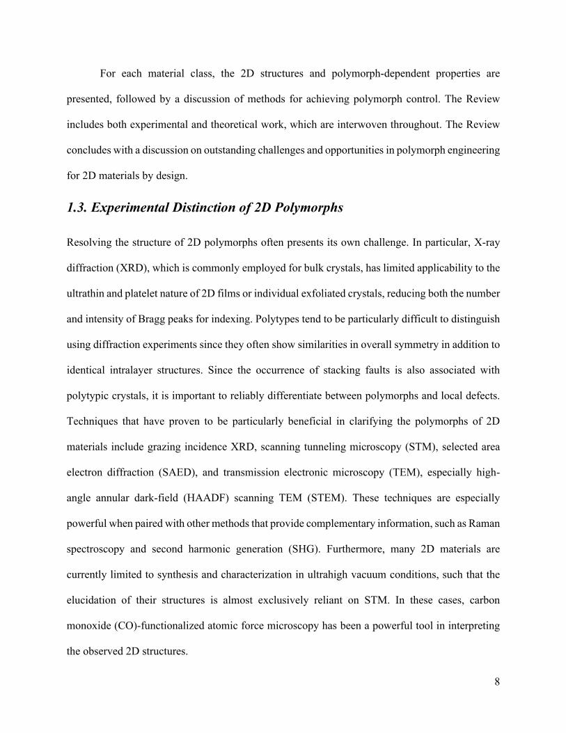
2.1.1. Structures and properties of 2D boron polymorphs
In the bulk, boron exhibits complex structures and several different polymorphs, although none of
these structures are layered. The complexity of boron structures is attributed to its trivalent
electronic configuration, forming highly diverse bonding motifs that have attracted the interest of
researchers for decades.36,37 As a result, several 2D boron polymorphs were predicted far before
the experimental realization of borophene using molecular beam epitaxy (MBE) on Ag(111).30,31
The borophene structures that have been synthetically realized thus far are based on the triangular
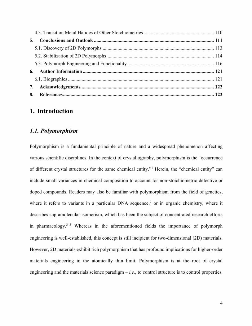
buckled lattice shown in Figure 1, which has a calculated unit cell of dimension a = 1.62 Å and b
= 2.85 Å with a buckling height of 0.86 Å.38 While this 2D structure was believed to be the most
stable for almost a decade,39,40 later work determined that a periodically defective derivative of the
triangular buckled lattice, known as the α sheet, was more energetically favorable.41,42 The α sheet
is a flat structure composed of hollow hexagons (HHs) with a vacancy concentration ν = m/N =

12
1/9 (Figure 1), where m is the number of HHs for N triangular lattice sites. The structures of
borophene are often referred to by their HH concentration, such that the pristine triangular buckled
structure and the α sheet correspond to ν0 and ν1/9 phases, respectively. The α sheet has a calculated
unit cell of dimension a = b = 5.05 Å, and Wu et al. found that a slight buckling of ± 0.17 Å makes
the structure more stable.43 Since the HH regions act as electron acceptors and the pristine
triangular regions acts as donors, the two motifs complement each other to form a more stable
overall structure.41
Subsequent studies found polymorphs with higher vacancy concentrations (ν > 1/9) to be
slightly more energetically favorable.43–46 A computational study by Penev et al. indicated that
buckling is present for structures of ν < 1/9, while higher HH concentrations are flat,44 although
slight buckling can occur when placed on a substrate.47 Calculations show that HH-based
structures are separated by small energetic differences, implying that coexistence of polymorphs
can be expected at finite temperatures.44,46 Indeed, the observed MBE-synthesized structures
contain HHs, with the most commonly reported structures being the β12 sheet (ν1/6) and the χ3 sheet
(ν1/5) on Ag(111). The ν1/6 and ν1/5 phases are also referred to as the S1 and S2 phases, respectively.
The HH concentration notation is used in this text to identify the polymorphs shown in Figure 1.
However, multiple HH arrangements can exist for a certain HH concentration.43 In the case of
borophene on Ag(111), the ν1/6 and ν1/5 exhibit the specific arrangements of the β12 and χ3 sheets
shown in Figure 1. The ν1/6 monolayer has a rectangular unit cell (calculated lattice parameters of
a = 2.92 Å, b = 5.08 Å), while the ν1/5 monolayer has a hexagonal unit cell (calculated lattice
parameters of a = b = 4.55 Å).38 While the exact structures of the borophene phases on Ag(111)
were ambiguous when initially observed with conventional STM, Liu et al. later used atomic force
microscopy with a CO-functionalized tip to directly image the spatial distribution of HHs.48 The
13
authors determined that the ν1/6 and ν1/5 models account for all observed phases on Ag(111), with
crystallographic rotations with respect to the substrate giving rise to the various STM observations.
Overall, experimental efforts have confirmed polymorphism in borophene, and the challenge now
lies in realizing synthetic conditions that enable phase purity or periodic polymorph superlattices.
The 2D boron polymorphs observed experimentally are all metallic in character, which is
consistent with multiple computational studies.44,41,30,49,50 A potential exception is the α sheet (ν1/9),
which Wu et al. calculated to be a narrow bandgap semiconductor,43 but the experimental
observation of this structure requires further investigation.51 In a study by Silvestre et al., the ν0
structure was found to exhibit a more anisotropic band structure than the ν1/6 and ν1/5 structures.52
Additionally, the authors found that the π* states in the ν1/6 structure are more localized than in the
ν1/5 structure. However, the distinctions are subtle and experimental measurements show that the
ν1/6 and ν1/5 structures on Ag(111) are electronically similar.30,48 Evidence of Dirac fermions in the
ν1/6 and ν1/5 structures has also been reported,53,54 although a large mismatch exists for the ν1/6
structure between the observed and predicted Dirac point with respect to the Fermi level. Gupta et
al. proposed that the observation of the Dirac-like dispersion in the ν1/6 phase on Ag(111) is due to
a predicted topologically nontrivial Dirac nodal line.55 The authors also predicted the existence of
two Dirac cones in ν1/6 borophene, which become gapped on Ag(111).
Superconductivity has also been predicted for the ν0, ν1/9, ν1/6, and ν1/5 borophene structures
with the transition temperature being polymorph dependent.56–58 While the predicted transition
temperatures are around 10-20 K in the freestanding monolayers, the interaction with an Ag(111)
substrate could reduce the values down to below 5 K. The presence of Dirac fermions59,60 and
superconductivity61 is also predicted for other borophene polymorphs that have not yet observed
experimentally but could be stabilized by a metal substrate. The HH concentration also has an
14
effect on the thermal and mechanical properties of borophene.62–64 In particular, the ν1/6 polymorph
has been calculated to possess an exceptionally high in-plane modulus to bending stiffness ratio
(568 nm-2), indicating a highly flexible material. Additionally, reports by Kulish et al.65 and Xiang
et al.66 detail the polymorph-dependent chemical properties of borophene, which include surface
reactivity and metal ion adsorption and migration. Kulish et al. found that the ν1/6 phase is generally
more reactive than the ν1/9 and ν0 phases, while Xiang et al. contend that the ν0 phase shows more
anisotropic metal ion migration pathways in comparison to other borophene structures. For further
reading on the synthesis, properties, and applications of borophene, please see the reviews by
Mannix et al.,36 Zhang et al.,37 and Li et al.67
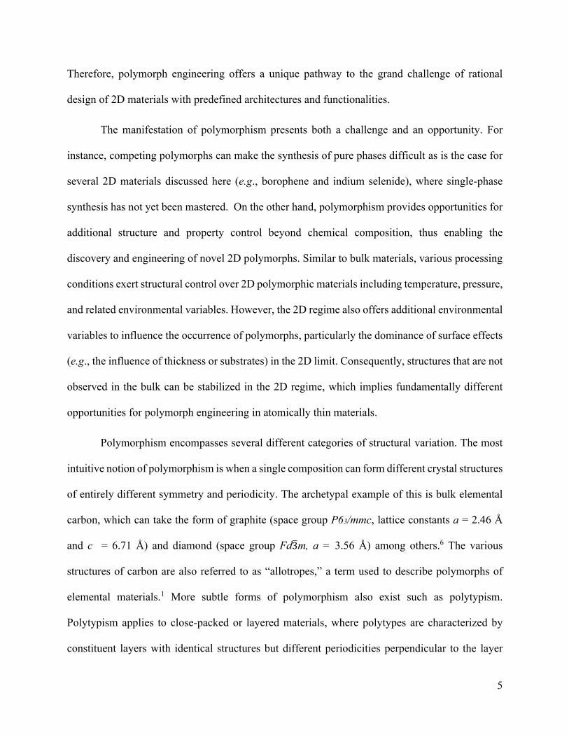
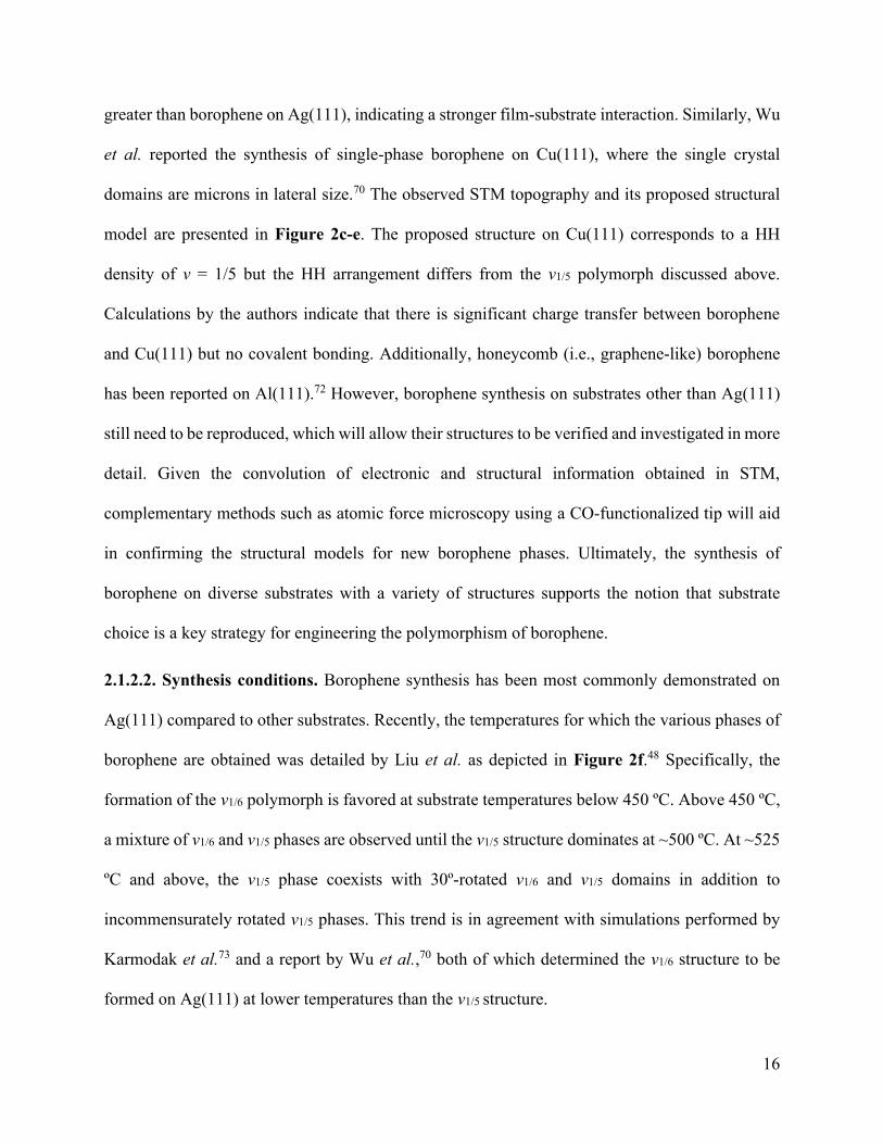
Figure 1. 2D polymorphs of borophene. Commonly reported monolayer polymorphs of borophene. The
ν1/6 and ν1/5 structures have been experimentally observed on Ag(111). Modification of the buckled
triangular (ν0) structure with various HH concentrations results in the other presented polymorphs.
2.1.2. Polymorph control of 2D boron
2.1.2.1. Substrates. Since 2D boron is metastable, its growth requires the presence of a stabilizing
substrate. So far, metallic substrates have played that role and are thus critical in experimentally
accessing 2D borophene polymorphs. In particular, borophene is thought to be stabilized by the
charge transfer and chemical hybridization provided by metal substrates.68 Silver was predicted as
a suitable substrate prior to its use in the first borophene growth experiments. Liu et al. had

15
suggested the use of Ag or Au based on the lack of boride formation and sufficiently strong
interaction with boron for surface adhesion while still promoting a 2D, rather than 3D, growth
mode for boron superstructures.69 Furthermore, depending on the type of metal, different HH
concentrations are favored.68 In this manner, the substrate can provide a borophene polymorph
selection mechanism. Since Ag, Cu, and Ni donate electrons to borophene, these substrates are
expected to favor the formation of borophene with a high HH concentration. On the other hand,
since Au withdraws electrons, lower HH concentrations are expected. This trend is supported by
the observation of ν1/6 and ν1/5 structures on Ag(111)48 and ν1/12 structures on Au(111).50 Currently,
Ag(111) is the most prevalent substrate for borophene growth. The observed borophene phases on
Ag(111) can be assigned to either ν1/6 or ν1/5 structures, both of which can adopt various rotational
orientations with respect to the metal substrate.48 A report by Campbell et al. verified that the ν1/6
and ν1/5 polymorphs on Ag(111) are chemically discrete from the Ag(111) substrate and described
by a relatively weak film-substrate interaction. Experimental images of the ν1/6 and ν1/5 structures
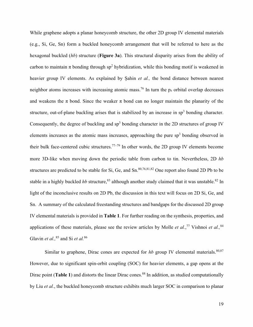
obtained from atomic force microscopy using a CO-functionalized tip are shown in Figure 2a.
Furthermore, multiple studies report the coexistence of the ν1/6 and ν1/5 structures, attesting to the
polymorphism of borophene.25,30,31,70 An STM image of a region containing intermixed ν1/6 and
ν1/5 domains is presented in Figure 2b. As suggested by Silvestre et al., the formation of
periodically alternating domains of the ν1/6 and ν1/5 phases could be leveraged to form electronic
stripes or transport channels.52
In contrast to Ag(111), Vinogradov et al. observed only a single a phase of borophene
grown via MBE on Ir(111).71 The proposed structure for their STM observations consists of a HH
density of ν = 1/6, however the HHs are arranged differently from the ν1/6 polymorph discussed
above. The authors calculated the exfoliation energy for borophene on Ir(111) to be five times
16
greater than borophene on Ag(111), indicating a stronger film-substrate interaction. Similarly, Wu
et al. reported the synthesis of single-phase borophene on Cu(111), where the single crystal
domains are microns in lateral size.70 The observed STM topography and its proposed structural
model are presented in Figure 2c-e. The proposed structure on Cu(111) corresponds to a HH
density of ν = 1/5 but the HH arrangement differs from the ν1/5 polymorph discussed above.
Calculations by the authors indicate that there is significant charge transfer between borophene
and Cu(111) but no covalent bonding. Additionally, honeycomb (i.e., graphene-like) borophene
has been reported on Al(111).72 However, borophene synthesis on substrates other than Ag(111)
still need to be reproduced, which will allow their structures to be verified and investigated in more
detail. Given the convolution of electronic and structural information obtained in STM,
complementary methods such as atomic force microscopy using a CO-functionalized tip will aid
in confirming the structural models for new borophene phases. Ultimately, the synthesis of
borophene on diverse substrates with a variety of structures supports the notion that substrate
choice is a key strategy for engineering the polymorphism of borophene.
2.1.2.2. Synthesis conditions. Borophene synthesis has been most commonly demonstrated on
Ag(111) compared to other substrates. Recently, the temperatures for which the various phases of
borophene are obtained was detailed by Liu et al. as depicted in Figure 2f.48 Specifically, the
formation of the ν1/6 polymorph is favored at substrate temperatures below 450 ºC. Above 450 ºC,
a mixture of ν1/6 and ν1/5 phases are observed until the ν1/5 structure dominates at ~500 ºC. At ~525
ºC and above, the ν1/5 phase coexists with 30º-rotated ν1/6 and ν1/5 domains in addition to
incommensurately rotated ν1/5 phases. This trend is in agreement with simulations performed by
Karmodak et al.73 and a report by Wu et al.,70 both of which determined the ν1/6 structure to be
formed on Ag(111) at lower temperatures than the ν1/5 structure.

17
While similar temperatures are used for the synthesis of borophene on Au(111), Kiraly et
al. reported that the total dose of boron required was an order of magnitude greater than on
Ag(111). The authors attributed this discrepancy to dissolution of boron into the bulk of the Au
substrate, which later segregates to the surface upon cooling. Similarly, dissolution of boron into
Ir(111) was reported by Vinogradov et al., such that 3D boron clusters segregate to the surface
after excessive boron dosing.71 Recrystallization from subsurface boron in Cu(111) was also
reported by Wu et al.74 Further studies are needed to fully understand the surface segregation
synthesis mechanism for borophene and its implications for polymorphic control.
2.1.2.3. Post-synthesis processing. The structure of borophene can also be modified through
additional processing following boron deposition. For example, thermal post-annealing of
borophene domains at 650 K has been demonstrated to convert most ν1/6 domains to the ν1/5
structure,31 which is in agreement with the ν1/5 phase being favored at higher temperatures during
growth. Moreover, Zhang et al. suggested that charge doping via a gate voltage could alter the HH
concentration of borophene monolayers.75 This concept is based on the previously discussed
formation of HHs in borophene as a self-doping mechanism that contributes to structural stability.
External control of the charge doping with a gate voltage could provide a dynamic method for
polymorph control in borophene, although this intriguing possibility has not yet been demonstrated
experimentally.

18
Figure 2. Experimental demonstrations of polymorphic control in borophene. a) Ultra-high vacuum
atomic force microscopy images obtained using a CO-functionalized tip of the ν1/6 – 30° and ν1/5 phases of
borophene grown on Ag(111) via MBE. The simulated atomic force microscopy images, overlaid with the
structural models, are shown on the left of each image, and the experimental images are shown on the right.
The scale bars for the ν1/6 – 30° and ν1/5 images are 5 Å and 2 Å, respectively. b) Bare-tipped STM image
of the coexistence of the ν1/6 (red) and ν1/5 (blue) borophene phases on Ag(111). The scale bar is 2 nm. c)
STM image obtained with a CO-functionalized tip of borophene grown on Cu(111) via MBE. Growth on
Cu(111) is reported to promote large domains of single-crystal borophene without competing phases. d)
DFT-simulated image of the constant tunneling current isosurface corresponding to the proposed borophene
structure in e). The proposed structure has a HH concentration of ν = 1/5, but the HH arrangement is
different from the ν1/5 phase of borophene on Ag(111). The unit cell is outlined in black and has a dimension
of 15.96 Å × 21.84 Å. f) Phases of borophene obtained via MBE on Ag(111) at different temperatures.
Increasing the substrate temperature during deposition results in the coexistence of multiple phases,
including ν1/5 structures that are rotationally incommensurate to the underlying Ag(111) substrate
crystallography (denoted by ν1/5-α where α is an arbitrary angle). a), b), and f) are adapted from Ref.48
Copyright 2019 Springer Nature under a Creative Commons Attribution 4.0 International License
https://creativecommons.org/licenses/by/4.0. c-e) are adapted with permission from Ref.70 Copyright 2018
Springer Nature.
2.2. Group IV Elements
2.2.1. Structures and properties of 2D group IV elemental polymorphs
19
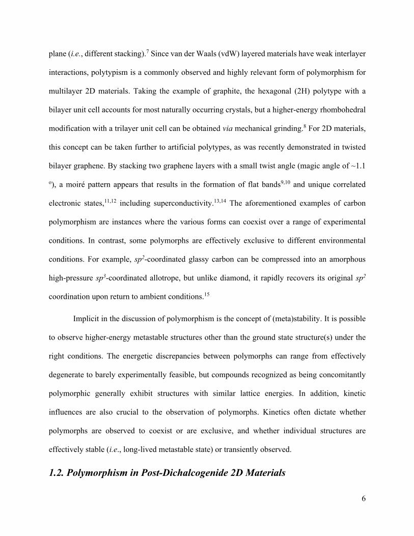
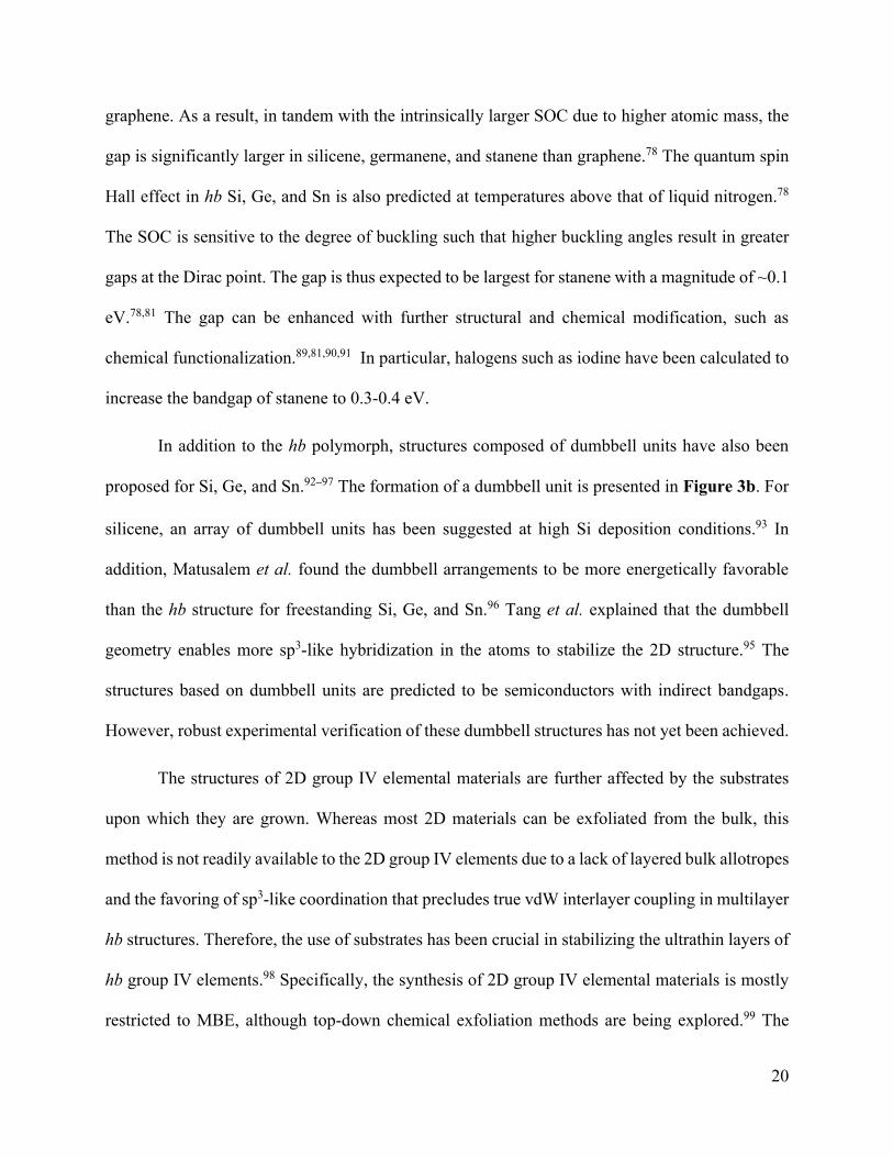
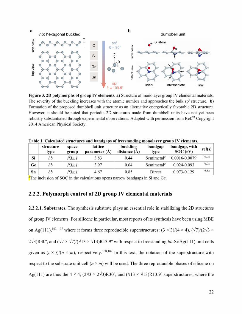
While graphene adopts a planar honeycomb structure, the other 2D group IV elemental materials
(e.g., Si, Ge, Sn) form a buckled honeycomb arrangement that will be referred to here as the
hexagonal buckled (hb) structure (Figure 3a). This structural disparity arises from the ability of
carbon to maintain π bonding through sp2 hybridization, while this bonding motif is weakened in
heavier group IV elements. As explained by Şahin et al., the bond distance between nearest
neighbor atoms increases with increasing atomic mass.76 In turn the pz orbital overlap decreases
and weakens the π bond. Since the weaker π bond can no longer maintain the planarity of the
structure, out-of-plane buckling arises that is stabilized by an increase in sp3 bonding character.
Consequently, the degree of buckling and sp3 bonding character in the 2D structures of group IV
elements increases as the atomic mass increases, approaching the pure sp3 bonding observed in
their bulk face-centered cubic structures.77–79 In other words, the 2D group IV elements become
more 3D-like when moving down the periodic table from carbon to tin. Nevertheless, 2D hb
structures are predicted to be stable for Si, Ge, and Sn.80,76,81,82 One report also found 2D Pb to be
stable in a highly buckled hb structure,83 although another study claimed that it was unstable.82 In
light of the inconclusive results on 2D Pb, the discussion in this text will focus on 2D Si, Ge, and
Sn. A summary of the calculated freestanding structures and bandgaps for the discussed 2D group
IV elemental materials is provided in Table 1. For further reading on the synthesis, properties, and
applications of these materials, please see the review articles by Molle et al.,77 Vishnoi et al.,84
Glavin et al.,85 and Si et al.86
Similar to graphene, Dirac cones are expected for hb group IV elemental materials.80,87
However, due to significant spin-orbit coupling (SOC) for heavier elements, a gap opens at the
Dirac point (Table 1) and distorts the linear Dirac cones.88 In addition, as studied computationally
by Liu et al., the buckled honeycomb structure exhibits much larger SOC in comparison to planar
20
graphene. As a result, in tandem with the intrinsically larger SOC due to higher atomic mass, the
gap is significantly larger in silicene, germanene, and stanene than graphene.78 The quantum spin
Hall effect in hb Si, Ge, and Sn is also predicted at temperatures above that of liquid nitrogen.78
The SOC is sensitive to the degree of buckling such that higher buckling angles result in greater
gaps at the Dirac point. The gap is thus expected to be largest for stanene with a magnitude of ~0.1
eV.78,81 The gap can be enhanced with further structural and chemical modification, such as
chemical functionalization.89,81,90,91 In particular, halogens such as iodine have been calculated to
increase the bandgap of stanene to 0.3-0.4 eV.
In addition to the hb polymorph, structures composed of dumbbell units have also been
proposed for Si, Ge, and Sn.92–97 The formation of a dumbbell unit is presented in Figure 3b. For
silicene, an array of dumbbell units has been suggested at high Si deposition conditions.93 In
addition, Matusalem et al. found the dumbbell arrangements to be more energetically favorable
than the hb structure for freestanding Si, Ge, and Sn.96 Tang et al. explained that the dumbbell
geometry enables more sp3-like hybridization in the atoms to stabilize the 2D structure.95 The
structures based on dumbbell units are predicted to be semiconductors with indirect bandgaps.
However, robust experimental verification of these dumbbell structures has not yet been achieved.
The structures of 2D group IV elemental materials are further affected by the substrates
upon which they are grown. Whereas most 2D materials can be exfoliated from the bulk, this
method is not readily available to the 2D group IV elements due to a lack of layered bulk allotropes
and the favoring of sp3-like coordination that precludes true vdW interlayer coupling in multilayer
hb structures. Therefore, the use of substrates has been crucial in stabilizing the ultrathin layers of
hb group IV elements.98 Specifically, the synthesis of 2D group IV elemental materials is mostly
restricted to MBE, although top-down chemical exfoliation methods are being explored.99 The
21
strong film-substrate interactions in MBE-grown group IV elemental films can result in
reconstructions that deviate from the structure of their calculated freestanding forms.
Consequently, polymorphism in the 2D group IV elements includes the various reconstructions or
superstructures observed due to coupling with their substrates. Moreover, the sensitivity of these
materials to ambient conditions limits most of their characterization to STM and other in situ ultra-
high vacuum (UHV) techniques, which complicates the verification of their observed 2D
structures. Consequently, significant controversy exists in the literature concerning the structures
and compositions of the materials reported as silicene, germanene, and stanene.
The structural modifications induced in 2D group IV elements by growth substrates in turn
affect their symmetry and electronic properties. For example, Lin et al. found that the 4 × 4 silicene
superstructure on Ag(111) breaks the symmetry of pristine hb-silicene resulting in a loss of Dirac
fermion characteristics.100 While hb-stanene is predicted to exhibit a narrow bandgap, the growth
of stanene on Bi2Te3(111) renders it metallic due to the topologically metallic states of the
substrate.101 While the influence of the substrate often leads to discrepancies between observations
and theoretical predictions of the free-standing material, these discrepancies sometimes provide
enhanced functionality. For example, Liao et al. recently demonstrated superconductivity in few-
layer stanene on PbTe(111)/Bi2Te3 substrates where the thickness of the PbTe(111) layer enabled
modulation of the superconducting behavior.102
22
Figure 3. 2D polymorphs of group IV elements. a) Structure of monolayer group IV elemental materials.
The severity of the buckling increases with the atomic number and approaches the bulk sp3 structure. b)
Formation of the proposed dumbbell unit structure as an alternative energetically favorable 2D structure.
However, it should be noted that periodic 2D structures made from dumbbell units have not yet been
robustly substantiated through experimental observations. Adapted with permission from Ref.93 Copyright
2014 American Physical Society.
Table 1. Calculated structures and bandgaps of freestanding monolayer group IV elements.
structure
type
space
group
lattice
parameter (Å)
buckling
distance (Å)
bandgap
type
bandgap, with
SOC (eV) ref(s)
Si hb P3m1 3.83 0.44 Semimetala 0.0016-0.0079 76,78
Ge hb P3m1 3.97 0.64 Semimetala 0.024-0.093 76,78
Sn hb P3m1 4.67 0.85 Direct 0.073-0.129 78,82 aThe inclusion of SOC in the calculations opens narrow bandgaps in Si and Ge.
2.2.2. Polymorph control of 2D group IV elemental materials
2.2.2.1. Substrates. The synthesis substrate plays an essential role in stabilizing the 2D structures
of group IV elements. For silicene in particular, most reports of its synthesis have been using MBE
on Ag(111),103–107 where it forms three reproducible superstructures: (3 × 3)/(4 × 4), (√7)/(2√3 ×
2√3)R30º, and (√7 × √7)/(√13 × √13)R13.9º with respect to freestanding hb-Si/Ag(111) unit cells
given as (i × j)/(n × m), respectively.108,109 In this text, the notation of the superstructure with
respect to the substrate unit cell (n × m) will be used. The three reproducible phases of silicene on
Ag(111) are thus the 4 × 4, (2√3 × 2√3)R30º, and (√13 × √13)R13.9º superstructures, where the

23
Rθº notation indicates a rotation of the overlayer lattice of θ degrees with respect to the substrate
lattice. Pawlak et al. recently utilized atomic force microscopy with a CO-functionalized tip to
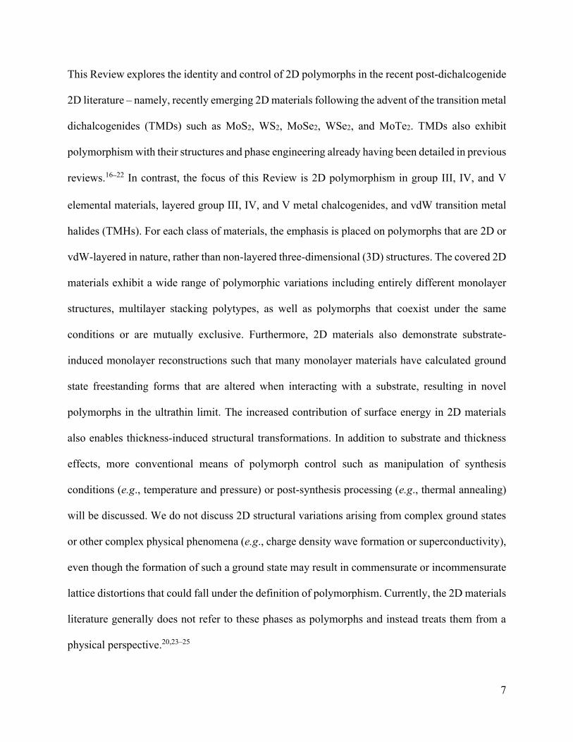
image these three structures (Figure 4a).108 The 4 × 4 phase is the most stable and studied phase,109
and is generally believed to correspond to hb-Si with a buckling of about 0.8 Å.108 Additionally,
the synthesis of silicene has been reported on Ir(111),110 Ru(001),111 ZrBr2(001),112 ZrC(111),113
and Pb(111).114 Compared to silicene, the number of studies of germanene synthesis are fewer, but
most of them also employ metallic substrates. Germanene was first reported using MBE on Pt(111)
as a √19×√19 superstructure.115 Subsequently, germanene synthesis has been pursued using MBE
on additional metal substrates such as Au(111),116–118 Ag(111),119,120 Al(111), 121–123 Cu(111)124
and Sb(111).125 Stanene synthesis has also been reported on metallic substrates such as Sb(111),126
Cu(111),127 Ag(111),128 and Au(111), where multiple phases have been observed in the latter
case.129,130 Additionally, stanene synthesis has been achieved on semiconducting substrates. Due
to commensurate lattices, the synthesis of hb-stanene without a reconstruction was achieved by
Zhu et al. with MBE on a Bi2Te3(111) substrate,101 although compressive strain increased the
buckling of the hb structure to 1.2 Å instead of the expected value of 0.85 Å for freestanding hb-
stanene. In this case, stanene was found to be metallic due to metallic Bi2Te3 surface states. In later
reports, the epitaxial growth of hb-Sn on PbTe(111)/Bi2Te3(111) was also demonstrated where the
stanene pz orbitals are hybridized with both the substrate on the bottom (Te-terminated PbTe(111))
and presumed hydrogen functionalization on top. The authors attribute the resulting sizeable
bandgap of 0.32 eV to the presumed hydrogen passivation, which also imparted high chemical
stability in ambient conditions. Since stanene grows epitaxially on PbTe(111), Zang et al. were
able to change the lattice constant of the stanene from an estimated 4.46 Å to 4.52 Å by changing
the thickness of the underlying PbTe(111) layer on Bi2Te3. Liao et al. similarly used the thickness
24
of the PbTe(111) substrate to tune the superconducting transition temperature of passivated
multilayer stanene on PbTe(111)/Bi2Te3(111).102 The epitaxial growth of few-layer stanene films
has also been investigated on semiconducting InSb(111), where evidence of 2D Dirac-like cones
were observed by Xu et al.,131 and a topologically nontrivial band structure was observed by Xu
et al.132 and Rogalev et al.133 Finally, vdW substrates such as highly oriented pyrolytic graphite
(HOPG)134 and MoS2135 have been utilized for the growth of silicene and germanene, but the results
have been mixed, presumably due to insufficiently strong film-substrate interactions.136,137
In contrast to pure vdW materials, the 2D group IV elements require additional
stabilization, which explains why metal substrates have been most widely employed. For example,
Gao et al. studied the growth mechanism of silicene on Ag (111) and found that initial silicene
clusters were stabilized by the Ag(111) surface as a result of the passivation of unsaturated edge
Si atoms by Ag free electrons and the p-d hybridization between inner Si atoms and the Ag
substrate.138 Hence, strong film-substrate interactions appear necessary to obtain the hb structure
in group IV elements.139 When weakly interacting vdW substrates are used, the formation of bulk-
like silicon or germanium clusters has been reported.136,137,140 While metal substrates can provide
the strength of interaction necessary for stabilization, they strongly disturb the Dirac states and
other intrinsic properties. Indeed, many reports suggest that the Dirac-like cones for silicene are
destroyed on Ag(111) substrates by Si-Ag hybridization,141,142,100,143,144 although the topic is still
debated.145 Similarly, a computational study by Wang et al. concluded that many metal substrates
destroy the Dirac cones in germanene,146 which may explain why conclusive experimental
observation of Dirac-like cones in germanene have not yet been achieved.
Strong substrate interactions also make the 2D group IV elements susceptible to the
formation of surface alloys. Along these lines, several studies of the structure of (√3 × √3)R30º
25
silicene on Ag(111) obtained at high temperatures have suggested that this phase is a bulk-like
silicon terminated with a Ag surface alloy rather than multilayer silicene.147–152 Similarly, the
observed structures of germanene and stanene on several metal substrates are purportedly surface
alloys, rather than hb-germanene or hb-stanene reconstructions, including germanium on
Pt(111),153,154 Au(111),155,156 and Al(111),157–159 as well as tin on Ag(111).160
The strength of interaction between the group IV element and the substrate also has
implications for the degree of buckling observed. Deng et al. used a strongly interacting Cu(111)
substrate to synthesize a planar honeycomb stanene film instead of the buckled structure (Figure
4b).161 The planar structure is not reconstructed and corresponds to a 2 × 2 Cu(111) supercell. The
authors calculated the adsorption energy of the Sn atoms to the Cu(111) substrate as ~1.16
eV/atom, which is considerably higher than the calculated binding energies for Si on Ag(111) of
~0.7 eV/atom. The authors thus attribute the stanene planarity in this case to the energetically
favorable maximization of all Sn atoms in contact with the Cu(111) surface. This structure has
been predicted to enable topologically derived boundary states, which is consistent with the
scanning tunneling spectroscopy (STS) results shown in Figure 4c. In particular, STS indicates
the presence of an edge state in an energy range that matches the energy of the SOC-induced gap
observed in angle-resolved photoemission spectroscopy (ARPES) experiments (−1.25 eV ± 0.15
eV).
Overall, the search for substrates that can stabilize the 2D group IV elemental materials
without destroying their predicted intrinsic properties remains a challenge. Future experimental
efforts may be guided by the many substrates that have been predicted to preserve the Dirac-like
dispersion expected from the freestanding hb structures of the group IV elements including
Al2O3(001),139 H-terminated SiC,162 Cl-terminated SiC,163 epitaxial graphene on SiC,164,165
26
hBN,162,166 CaF2,163 and CdTe.167 A more detailed discussion on the prospects of synthesizing
ultrathin films of group IV elements on non-metallic substrates is given in a review by Galbiati et
al.168
2.2.2.2. Synthesis conditions. The deposition conditions used during the synthesis of 2D group
IV elements also affect their structure and composition. For example, the deposition temperature
of Si on Ag(111) can be used to select for one silicene superstructure over another, although the
control is limited since coexistence of phases is often observed. In particular, a dominant 4 × 4
phase can be obtained at lower substrate temperatures around 470-600 K.105–107 The (2√3 ×
2√3)R30º and (√13 × √13)R13.9º superstructures are reported to coexist with the 4 × 4 phase at
higher temperatures with the (2√3 × 2√3)R30º phase generally becoming dominant with increasing
temperature.106,109 Increasing the deposition temperatures above 600 K results in the formation of
bulk-like silicon terminated with a Ag-Si alloy,151,169,170 while exceedingly low temperatures (<
400 K) result in disordered deposition.171 Similarly, the formation of Ge alloys with the substrate
is reported for temperatures above 900 K on Pt(111)154 and 600 K on Au (111).117 For the synthesis
of stanene on PbTe(111), a deposition procedure has been developed to prevent diffusion of Sn
atoms into the substrate lattice. Specifically, Zang et al. used a low-temperature deposition of Sn
on PbTe(111) at 150 K followed by a post-anneal a 400 K to obtain hb-stanene.172 A previous
study by Liang et al. also found that alloying of Sn on Cu (111) could be prevented by decreasing
the substrate temperature from 300 K to 100 K. While alloy formation was not discussed by Deng
et al., their procedure entailed Sn deposition on Cu(111) at 200 K.161 The authors report that
temperatures below 243 K are necessary to maintain the planar structure of stanene and that
domains of the buckled phase are obtained at higher temperatures. However, the previous study

27
by Liang et al. suggests that Sn-Cu alloy formation is another factor that dictates the optimal
deposition temperature, in addition to the planarity of the stanene structure.
Structural control over 2D group IV elements can also be achieved using the deposition
rate and/or coverage. For example, the silicene (√13 × √13)R13.9º structure on Ag(111) can be
obtained at the same conditions as the 4 × 4 superstructure for longer deposition times.105 A study
by Arafune et al. on the phase evolution of silicene structures on Ag(111) illustrates the dynamic
nature of silicene growth as a function of deposition time. The authors observed that a film of
primarily 4 × 4 hb-silicene on Ag(111) transitioned to a mixture of 4 different superstructures upon
further deposition of Si.107 Similarly, a structural evolution of silicene from a herringbone
arrangement to a honeycomb √7 × √7 superstructure on Ru(001) has been reported upon increased
Si coverage.111 The effect of deposition coverage on the structure of germanium domains on
Ag(111) was investigated by Lin et al., which considered the interesting case of dealloying. Initial
Ge deposition (< 1/3 of a monolayer) proceeded via the formation of an Ag2Ge alloy with further
deposition resulting in a dealloying process.119 The dealloying began with a highly strained striped
germanium phase (Figure 4d, top) commensurate with the Ag(111)-(√3 × √3)R30º unit cell, where
further deposition resulted in the conversion of the striped domains to an incommensurate
honeycomb phase (Figure 4d, bottom) that resembles freestanding germanene. The authors found
that the structural change to the quasi-freestanding phase was accompanied with a transition to a
band structure resembling germanene, although Dirac cones were not observed. This structural
evolution was also observed by Chiniwar et al.120 Dealloying processes have also been reported
for stanene synthesis on Ag(111)128 and Au(111).130 Hence, it is possible to obtain films of hb
group IV elements on metal substrates that initially form an alloy through a dealloying process
28
upon additional deposition. However, this relatively complicated phase evolution leads to
challenges in achieving high homogeneity in the resulting 2D materials.
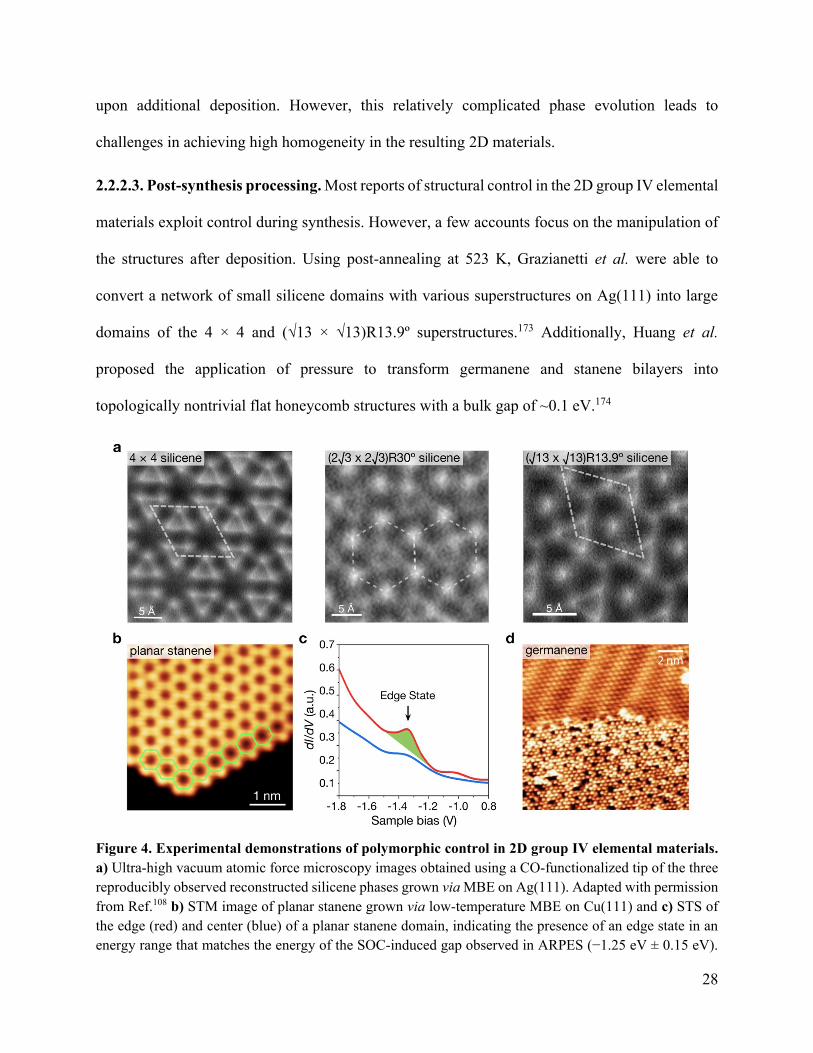
2.2.2.3. Post-synthesis processing. Most reports of structural control in the 2D group IV elemental
materials exploit control during synthesis. However, a few accounts focus on the manipulation of
the structures after deposition. Using post-annealing at 523 K, Grazianetti et al. were able to
convert a network of small silicene domains with various superstructures on Ag(111) into large
domains of the 4 × 4 and (√13 × √13)R13.9º superstructures.173 Additionally, Huang et al.
proposed the application of pressure to transform germanene and stanene bilayers into
topologically nontrivial flat honeycomb structures with a bulk gap of ~0.1 eV.174
Figure 4. Experimental demonstrations of polymorphic control in 2D group IV elemental materials.
a) Ultra-high vacuum atomic force microscopy images obtained using a CO-functionalized tip of the three
reproducibly observed reconstructed silicene phases grown via MBE on Ag(111). Adapted with permission
from Ref.108 b) STM image of planar stanene grown via low-temperature MBE on Cu(111) and c) STS of
the edge (red) and center (blue) of a planar stanene domain, indicating the presence of an edge state in an
energy range that matches the energy of the SOC-induced gap observed in ARPES (−1.25 eV ± 0.15 eV).
29
The stabilization of the planar polymorph was attributed to the strong interaction of Sn with the Cu(111)
substrate. Adapted with permission from Ref.161 Copyright 2018 Springer Nature. d) Coexistence of a
partially commensurate “striped” phase (top) and quasi-freestanding incommensurate honeycomb phase
(bottom) of germanene grown via MBE on Ag(111). The quasi-freestanding phase is reported to form after
the striped phase by dealloying of Ge from the Ag(111) surface upon further Ge deposition. Adapted with
permission from Ref.119 Copyright 2018 American Physical Society.
2.3. Group V Elements
2.3.1. Structures and properties of 2D group V elemental polymorphs
Many of the group V elemental materials (P, As, Sb, Bi), or pnictogens, exist as layered
polymorphs in the bulk that can be exfoliated into 2D form. In particular, there are three types of
monolayer structures observed in the layered elemental group V materials: hexagonal buckled
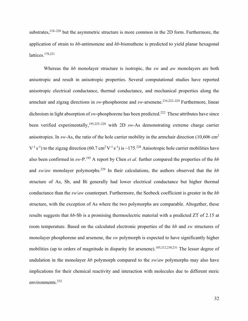
(hb), symmetric washboard (sw), and asymmetric washboard (aw) (Figure 5a). The hb structure
is the most symmetric of the three polymorphs and is analogous to that observed in the group IV
elemental 2D materials. Recall that this structure resembles the planar hexagonal lattice of
graphene, but with significant out-of-plane buckling such that there are two distinct atomic planes
in the monolayer structure. The monolayer hb structure can be converted to a graphene-like planar
hexagonal lattice if the buckling is eliminated with external forces, such as strain or chemical
functionalization.175–179 In its bulk form, the layered hb structure is known as the rhombohedral
A7 (Strukturbericht designation) or α-As structure type. At this point, it is important to make a
note regarding nomenclature of group V elemental structures. In the 2D material literature, the “β”
designation is often used to refer to the monolayer hb structure while “α” is used to refer to the
monolayer sw structure, which can cause confusion. For example, atomically thin α-As is
sometimes referred to as “β-As” in the 2D material literature, even though they both correspond
to the hb structure. To avoid this confusion, the “α” and “β” designations will not be used here to
30
identify 2D group V elemental polymorphs. The bulk A7 structure can be derived as a distortion
of the simple cubic structure with a rhombohedral shear and displacement along the [111]
direction.180 The distortion is explained by the existence of a Peierls electronic instability from the
half-filled p bands.181 While the intralayer bonding in the A7 (multilayer hb) structure is of much
greater strength than the interlayer bonding, the layers are not explicitly vdW-bonded and have a
weakly covalent nature that increases from As to Bi.182,183
The monolayer sw structure is also composed of six-membered rings, but they are puckered
into a chair-like confirmation. The result is an orthorhombic lattice with two distinct atomic planes.
This puckered structure is best known as the structure of monolayer black phosphorus
(phosphorene). The bulk black phosphorus structure is also referred to as the A17 structure
(Strukturbericht designation).184 The aw structure is similar to the sw structure, but with an
additional out-of-plane offset or buckling between neighboring atoms in the two atomic layers. As
a result, the aw polymorph is lower in symmetry with four distinct atomic planes in the monolayer.
The relationship between the A7 (hb) and A17 (sw/aw) polymorphs was investigated in a study by
Boulfelfel et al.184 The authors predicted the observation of sw/aw structures in other group V
elements with hb ground state structures (As, Sb, Bi). These predictions were later corroborated
by Zhang et al.185 in their computational assessment of the stability of 2D structures of the group
V elements and have since been confirmed experimentally. A summary of the commonly observed
monolayer group V polymorphs is presented in Figure 5b. Additionally, the existence of a square-
octagon polymorph for this class of materials composed of tiled square and octagonal rings of
atoms has been predicted by many but has yet to be observed experimentally.186–190 In contrast to
the other pnictogens, nitrogen does not exhibit a layered bulk solid. While nitrogen is usually
observed in a molecular form, a report has synthesized a covalently bonded cubic gauche phase of
31
nitrogen at extreme temperatures and pressures.191 The existence of a solid 2D phase of nitrogene
in the hb192 or square-octagon187 structure has been predicted, but not yet confirmed
experimentally, although attempts have been made in this direction.193
Phosphorus is the most widely studied of the group V elemental materials in the 2D
material literature. The layered sw polymorph, known as black phosphorus or α-P, is
thermodynamically stable at ambient conditions and usually formed at high pressure, although
synthesis at lower pressures has also been achieved.194 The investigation of 2D sw-P was enabled
in 2014 via mechanical exfoliation from bulk black phosphorus.195–197 At high pressures, the black
phosphorus structure transitions to the A7 structure (layered hb structure).198 While the hb structure
of phosphorus, named “blue phosphorus”, was predicted by Zhu et al. to be stable in the monolayer
form,199 top-down exfoliation is not possible for 2D hb-P since the bulk A7 structure is
thermodynamically unstable in ambient conditions. Consequently, the realization of 2D hb-P was
not achieved until 2016 through MBE on Au(111).200 As of now, MBE on Au(111) remains the
sole pathway through which 2D hb-P can be obtained, and a recent report has called this structure
into question.201 Outside of the sw and hb monolayers, several other 2D polymorphs have been
proposed in computational studies202–208 beyond the square-octagon structure.186
For the heavier group V elements (As, Sb, Bi), the most stable polymorph in the bulk is the
A7 (layered hb) structure.209 This form is also termed gray arsenic, gray antimony, and metallic
bismuth.210 In the bulk, elemental arsenic can also adopt a metastable layered sw (A17) structure.211
For 2D arsenene, several computational studies have predicted both the hb and sw monolayers to
be stable.212–214,189 Similarly, 2D antimonene and 2D bismuthene have been predicted to be stable
in the monolayer hb structure as well as the aw structure, the latter of which is not observed in the
bulk.215–218 For bismuthene, the sw form may also be obtained when stabilized with appropriate
32
substrates,218–220 but the asymmetric structure is more common in the 2D form. Furthermore, the
application of strain to hb-antimonene and hb-bismuthene is predicted to yield planar hexagonal
lattices.178,221
Whereas the hb monolayer structure is isotropic, the sw and aw monolayers are both
anisotropic and result in anisotropic properties. Several computational studies have reported
anisotropic electrical conductance, thermal conductance, and mechanical properties along the
armchair and zigzag directions in sw-phosphorene and sw-arsenene.216,222–224 Furthermore, linear
dichroism in light absorption of sw-phosphorene has been predicted.222 These attributes have since
been verified experimentally,195,225–228 with 2D sw-As demonstrating extreme charge carrier
anisotropies. In sw-As, the ratio of the hole carrier mobility in the armchair direction (10,606 cm2
V-1 s-1) to the zigzag direction (60.7 cm2 V-1 s-1) is ~175.228 Anisotropic hole carrier mobilities have
also been confirmed in sw-P.195 A report by Chen et al. further compared the properties of the hb
and sw/aw monolayer polymorphs.229 In their calculations, the authors observed that the hb
structure of As, Sb, and Bi generally had lower electrical conductance but higher thermal
conductance than the sw/aw counterpart. Furthermore, the Seebeck coefficient is greater in the hb
structure, with the exception of As where the two polymorphs are comparable. Altogether, these
results suggests that hb-Sb is a promising thermoelectric material with a predicted ZT of 2.15 at
room temperature. Based on the calculated electronic properties of the hb and sw structures of
monolayer phosphorene and arsenene, the sw polymorph is expected to have significantly higher
mobilities (up to orders of magnitude in disparity for arsenene).185,212,230,231 The lesser degree of
undulation in the monolayer hb polymorph compared to the sw/aw polymorphs may also have
implications for their chemical reactivity and interaction with molecules due to different steric
environments.232

33
While both the hb and sw polymorphs are centrosymmetric, the aw structure is
noncentrosymmetric. The breaking of inversion symmetry in the aw polymorph holds promise for
the emergence of spontaneous polarization. A report by Xiao et al. on aw-structured group V
elemental monolayers predicted sizable in-plane ferroelectricity and antiferroelectricity with Curie
temperatures above room-temperature.233 The aw-structured materials are also expected to display
other spontaneous polarization phenomena such as piezoelectricity, although the magnitude of
these additional polarizations is not yet known. In addition, a recent computational study by Guo
et al. has predicted large intrinsic SHG in aw monolayers.234
As atomic mass increases, SOC becomes more significant. Consequently, hb-Bi is
predicted to be a topological insulator.235–237 The existence of these topological nontrivial states is
also expected to be sensitive to structural modifications. For example, the application of strain in
hb-arsenene and hb-antimonene has been reported to result in topologically nontrivial states.238–241
Furthermore, hexagonal planar structures of antimonene and bismuthene have been proposed as
2D topological crystalline insulators.178 Accordingly, several studies have reported the observation
of conductive edge states in planar bismuthene,242 hb-bismuthene,243 and hb-antimonene films.244
In contrast, monolayer aw-Bi is anticipated to be trivial. However, Lu et al.219 reported the
existence of topological edge states when the aw structure of bismuthene approaches the higher
symmetry sw structure through weakening of out-of-plane buckling. The effects of different
stacking configurations in the 2D group V polymorphs have been studied in several computational
reports but not yet corroborated with experimental studies.214,245,246 A summary of the structures
and bandgaps for the discussed 2D group V elemental materials is provided in Table 2. For further
reading on the synthesis, properties, and applications of these materials, please see the review
articles by Gusmão et al.,194 Zhang et al.,247 Ersan et al.,248 Vishnoi et al.,84 and Wu and Hao.249
34
Figure 5. 2D polymorphs of group V elements. a) Monolayer polymorphs of layered group V (pnictogen)
elemental materials. The aw structure differs from the sw structure by an out-of-plane buckling in the two
atomic planes of the sw structure (see side view). b) Summary of the commonly observed polymorphs for
each element. Although reports exist of sw-bismuthene grown on substrates,219,220 the freestanding form has
been calculated to be unstable.218

35
Table 2. Structures and bandgaps of monolayer and bulk group V elements.
Monolayer Bulk
structure
type
lattice
parameters
(Å)
bandgap
(eV) name
structure
type
space
group
lattice
parameters
(Å)
bandgap
(eV) ref(s)
P
hb a = 3.326a 2-3a, c
1.1, on Au(111)
blue
phosphorus A7 R3m
a = 3.324a
c = 5.63a 1.1a,c 199,250
sw a = 3.32a
b = 4.58a
1.51a,b, 1.94a,b
2b
black
phosphorus A17 Cmca
a = 3.3164
b = 10.484
c = 4.3793
0.335b 222,251–253
As
hb a = 3.607a 2.10 a,c grey
arsenic A7 R3m
a = 3.7598
c = 10.5475 Semimetal 213,214,254
sw a = 3.677a
b = 4.765a 1.47a,c
black
arsenic A17 Cmca
a = 3.74a
b = 10.76a
c = 4.36a
0.31a,b 211,213,214,228
Sb
hb a = 4.04a 0.76a,c, 1.55a,c grey
antimony A7 R3m
a = 4.31
c = 11.27 Semimetal 215,216
aw a = 4.28a
b = 4.74a 0.28a,c, 0.34a,c -
distorted
A17 - - - 215,216
Bi
hb a = 4.38a 0.32a,b,
0.45a,c
metallic
bismuth A7 R3m
a = 4.546
c = 11.863 Semimetal 218,255,256
aw a = 4.55a
b = 4.94a 0.39a,c -
distorted
A17 - - - 218,255
a calculated value b direct bandgap c indirect bandgap
2.3.2. Polymorph control of 2D group V elemental materials
2.3.2.1. Synthesis conditions. Since many group V elemental materials exhibit several
polymorphs, including non-layered structures, precise control of the synthesis conditions is
necessary to prevent the formation of other phases. For example, a report by Smith et al. describes
the formation of red and pyrophoric white phosphorus during attempts at the vapor-phase synthesis
of 2D black phosphorus.257 The possibility of pyrophoric competing phases implies that the
formation of black (sw) phosphorus during vapor-phase synthesis is difficult and dangerous. As a
result, efforts at the synthesis of phosphorene have mostly focused on the conversion of thin films
of red phosphorus to the black phosphorus structure. This polymorphic conversion typically
requires high pressures and recent attempts have yielded thick films or thick nanoflakes, rather
than the desired continuous monolayer.257–259 Rajabali et al. avoided the high pressure pathway by
instead using plasma treatment at 300 ºC to crystallize red phosphorus films into thick black
phosphorus nanoflakes.260 Meanwhile, synthesis of hb-P has been limited to MBE on Au(111),
where the typical substrate temperature during deposition is between 180 ºC and 350 ºC.200,250,261
The lack of reports of hb-P on other substrates suggest that film-substrate interactions are the
dominant factor in realizing this phase as is discussed later in section 2.3.2.2.
The vapor-phase synthesis of 2D hb-As is also subject to the formation of alternate phases.
A recent report by Hu et al. concerning PVD of hb-As nanoflakes states that the growth
temperatures were specifically chosen to avoid impurity phases.262 In particular, temperatures
above 300 ºC are required to prevent a mixture of hb and sw arsenic, while slow cooling prevents
the formation of metastable and light-sensitive yellow arsenic. Consequently, the authors used a
growth temperature of 325 ºC in their study. This temperature range is in agreement with a
subsequent report on the MBE of monolayer hb-As on Ag(111) using substrate temperatures of
37
200 ºC to 350 ºC.263 On the other hand, the bottom-up synthesis of 2D sw-As has yet to be achieved.
Due to its metastability, the synthesis of bulk sw-As (black arsenic) requires stabilization by the
presence of impurities. While black arsenic is usually found as a rare mineral, Antonatos et al.
recently reported the synthesis of bulk sw-As using growth temperatures of 100-200 ºC with
mercury vapors.264 These bulk synthetic crystals can then be used as a source of 2D sw-As
following exfoliation.228,265 For bismuthene, the role of the substrate temperature during synthesis
has also been demonstrated to favor the formation of one polymorph over another. In particular,
pulsed laser deposition (PLD) of bismuth on substrates at room temperature resulted in aw-Bi,
whereas substrate temperatures of 100 ºC resulted in hb-Bi.266 Additionally, the authors of this
study found the film thickness to be an essential parameter in the polymorphic control of
bismuthene. Typically, the aw structure only exists below a few layers, as discussed further in
section 2.3.2.3. However, Jankowski et al. were able to obtain exclusively aw-Bi films up to 14
nm in thickness by cooling the substrate to 40 K during UHV growth using a Bi source.267 Growth
at a higher temperature of 400 K resulted in a competition between aw-Bi and hb-Bi domains,
while growth at 450 K and above favored hb-Bi exclusively.
2.3.2.2. Substrates. The role of the substrate has proven to be one of the main methods of
polymorphic control in the group V elemental materials. In the case of hb (blue) phosphorene, its
synthesis has only been achieved on Au(111), which suggests that this substrate plays a crucial
role in stabilizing the hb structure for phosphorus. A computational study by Han et al. showed
that the formation energy (Ef) of hb-P on Au(111) is significantly lower than freestanding hb-P,
and that hb-P is favored over sw-P on Au(111).268 The interaction of hb-phosphorene with the
Au(111) surface is also believed to strongly modulate its properties. Specifically, the structure of
hb-phosphorene is reconstructed as shown in Figure 6a, resulting in a significant difference
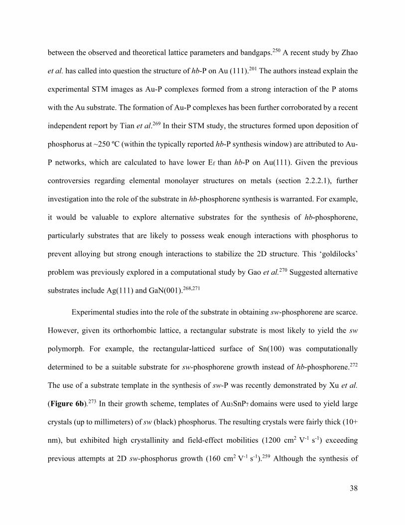
38
between the observed and theoretical lattice parameters and bandgaps.250 A recent study by Zhao
et al. has called into question the structure of hb-P on Au (111).201 The authors instead explain the
experimental STM images as Au-P complexes formed from a strong interaction of the P atoms
with the Au substrate. The formation of Au-P complexes has been further corroborated by a recent
independent report by Tian et al.269 In their STM study, the structures formed upon deposition of
phosphorus at ~250 ºC (within the typically reported hb-P synthesis window) are attributed to Au-
P networks, which are calculated to have lower Ef than hb-P on Au(111). Given the previous
controversies regarding elemental monolayer structures on metals (section 2.2.2.1), further
investigation into the role of the substrate in hb-phosphorene synthesis is warranted. For example,
it would be valuable to explore alternative substrates for the synthesis of hb-phosphorene,
particularly substrates that are likely to possess weak enough interactions with phosphorus to
prevent alloying but strong enough interactions to stabilize the 2D structure. This ‘goldilocks’
problem was previously explored in a computational study by Gao et al.270 Suggested alternative
substrates include Ag(111) and GaN(001).268,271
Experimental studies into the role of the substrate in obtaining sw-phosphorene are scarce.
However, given its orthorhombic lattice, a rectangular substrate is most likely to yield the sw
polymorph. For example, the rectangular-latticed surface of Sn(100) was computationally
determined to be a suitable substrate for sw-phosphorene growth instead of hb-phosphorene.272
The use of a substrate template in the synthesis of sw-P was recently demonstrated by Xu et al.
(Figure 6b).273 In their growth scheme, templates of Au3SnP7 domains were used to yield large
crystals (up to millimeters) of sw (black) phosphorus. The resulting crystals were fairly thick (10+
nm), but exhibited high crystallinity and field-effect mobilities (1200 cm2 V-1 s-1) exceeding
previous attempts at 2D sw-phosphorus growth (160 cm2 V-1 s-1).259 Although the synthesis of
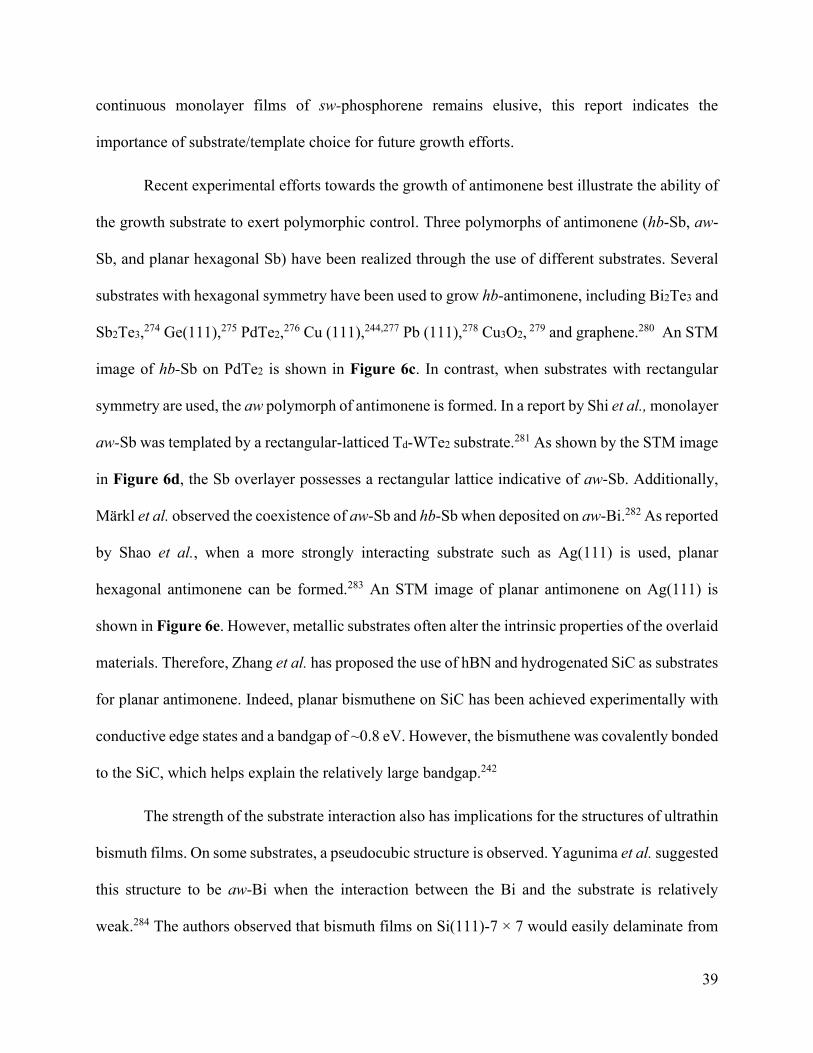
39
continuous monolayer films of sw-phosphorene remains elusive, this report indicates the
importance of substrate/template choice for future growth efforts.
Recent experimental efforts towards the growth of antimonene best illustrate the ability of
the growth substrate to exert polymorphic control. Three polymorphs of antimonene (hb-Sb, aw-
Sb, and planar hexagonal Sb) have been realized through the use of different substrates. Several
substrates with hexagonal symmetry have been used to grow hb-antimonene, including Bi2Te3 and
Sb2Te3,274 Ge(111),275 PdTe2,276 Cu (111),244,277 Pb (111),278 Cu3O2, 279 and graphene.280 An STM
image of hb-Sb on PdTe2 is shown in Figure 6c. In contrast, when substrates with rectangular
symmetry are used, the aw polymorph of antimonene is formed. In a report by Shi et al., monolayer
aw-Sb was templated by a rectangular-latticed Td-WTe2 substrate.281 As shown by the STM image
in Figure 6d, the Sb overlayer possesses a rectangular lattice indicative of aw-Sb. Additionally,
Märkl et al. observed the coexistence of aw-Sb and hb-Sb when deposited on aw-Bi.282 As reported
by Shao et al., when a more strongly interacting substrate such as Ag(111) is used, planar
hexagonal antimonene can be formed.283 An STM image of planar antimonene on Ag(111) is
shown in Figure 6e. However, metallic substrates often alter the intrinsic properties of the overlaid
materials. Therefore, Zhang et al. has proposed the use of hBN and hydrogenated SiC as substrates
for planar antimonene. Indeed, planar bismuthene on SiC has been achieved experimentally with
conductive edge states and a bandgap of ~0.8 eV. However, the bismuthene was covalently bonded
to the SiC, which helps explain the relatively large bandgap.242
The strength of the substrate interaction also has implications for the structures of ultrathin
bismuth films. On some substrates, a pseudocubic structure is observed. Yagunima et al. suggested
this structure to be aw-Bi when the interaction between the Bi and the substrate is relatively
weak.284 The authors observed that bismuth films on Si(111)-7 × 7 would easily delaminate from
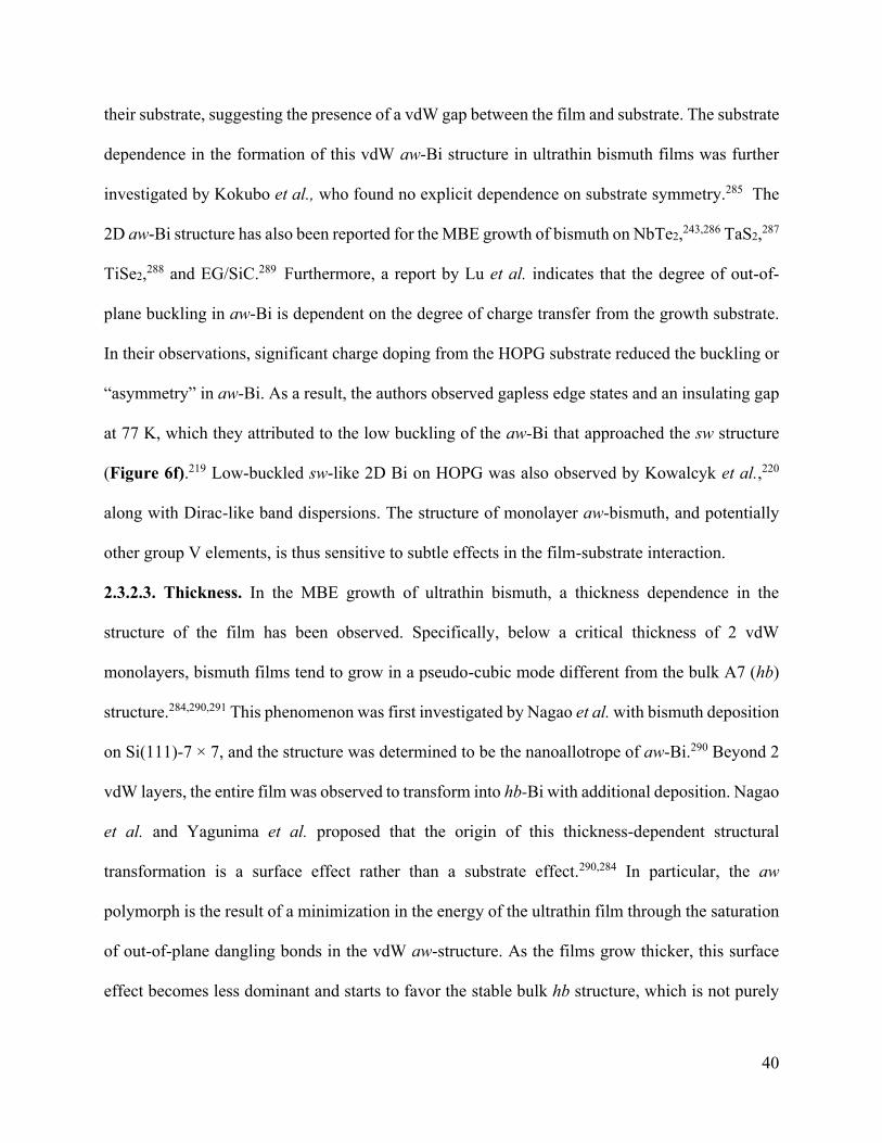
40
their substrate, suggesting the presence of a vdW gap between the film and substrate. The substrate
dependence in the formation of this vdW aw-Bi structure in ultrathin bismuth films was further
investigated by Kokubo et al., who found no explicit dependence on substrate symmetry.285 The
2D aw-Bi structure has also been reported for the MBE growth of bismuth on NbTe2,243,286 TaS2,287
TiSe2,288 and EG/SiC.289 Furthermore, a report by Lu et al. indicates that the degree of out-of-
plane buckling in aw-Bi is dependent on the degree of charge transfer from the growth substrate.
In their observations, significant charge doping from the HOPG substrate reduced the buckling or
“asymmetry” in aw-Bi. As a result, the authors observed gapless edge states and an insulating gap
at 77 K, which they attributed to the low buckling of the aw-Bi that approached the sw structure
(Figure 6f).219 Low-buckled sw-like 2D Bi on HOPG was also observed by Kowalcyk et al.,220
along with Dirac-like band dispersions. The structure of monolayer aw-bismuth, and potentially
other group V elements, is thus sensitive to subtle effects in the film-substrate interaction.
2.3.2.3. Thickness. In the MBE growth of ultrathin bismuth, a thickness dependence in the
structure of the film has been observed. Specifically, below a critical thickness of 2 vdW
monolayers, bismuth films tend to grow in a pseudo-cubic mode different from the bulk A7 (hb)
structure.284,290,291 This phenomenon was first investigated by Nagao et al. with bismuth deposition
on Si(111)-7 × 7, and the structure was determined to be the nanoallotrope of aw-Bi.290 Beyond 2
vdW layers, the entire film was observed to transform into hb-Bi with additional deposition. Nagao
et al. and Yagunima et al. proposed that the origin of this thickness-dependent structural
transformation is a surface effect rather than a substrate effect.290,284 In particular, the aw
polymorph is the result of a minimization in the energy of the ultrathin film through the saturation
of out-of-plane dangling bonds in the vdW aw-structure. As the films grow thicker, this surface
effect becomes less dominant and starts to favor the stable bulk hb structure, which is not purely

41
vdW layered. This phenomenon is in contrast to a substrate effect where a strong film-substrate
interaction forces a new structure. In fact, a pseudo-cubic structure explained by bulk-like hb
bonding, rather than aw bonding, is proposed for ultrathin bismuth films grown on more strongly
interacting substrates like β-√3 ×√3-Bi.284,285 Moreover, the observation of the aw-Bi structure
does not appear to depend explicitly on the substrate symmetry. For example, orthorhombic aw-
bismuthene was observed when grown via MBE on vdW-layered NbSe2 with six-fold symmetry
(Figure 6g). These observations support the mechanism of aw-Bi stabilization being a thickness
effect and prompts the question of how this phenomenon could be leveraged further. For example,
a report by Walker et al. proposed that the initial growth of vdW aw-Bi enables the facile dry
transfer of large-area single-crystal hb-Bi films from the Si(111) substrate.292 Overall, the
thickness-induced structural transformation in ultrathin bismuth films gives credence to the search
for 2D polymorphs not observed in the bulk.
2.3.2.4. Post-synthesis processing. Thermal treatments after the synthesis of 2D bismuth films
have been shown to result in structural conversions. For example, Kawakami et al. found that
annealing of aw-Bi films on Au(111) at 470 K transformed them into the hb structure.293 Jankowski
et al. observed a similar transitional temperature of 450 K with ultrathin bismuth films on c-plane
sapphire.267 These results indicate that the hb structure is more stable than the aw polymorph in
bismuth films, which is consistent with the absence of bulk aw-Bi. Given that the various 2D
polymorphs of phosphorene, arsenene, and antimonene also have different stabilities,294,189,216 the
use of cooling or heating could also be used in these cases to access different structures. However,
thermally induced structural transformations between polymorphs in these 2D materials have yet
to be investigated. Other post-synthesis treatments for controlling the structure of 2D group V
elements have been considered computationally. For instance, the functionalization of hb-

42
structured As, Sb, and Bi monolayers with hydrogen or halogens was predicted to convert the
structures to a planar hexagonal form.175,177,295 Additionally, the application of mechanical forces
or the introduction of defects have been suggested as pathways to access several novel
phosphorene polymorphs.199,296
Figure 6. Experimental demonstrations of polymorphic control in 2D group V elemental materials.
a) High-resolution STM image of hb (blue) phosphorene grown via MBE on Au(111). Due to strong
interaction with the Au(111) substrate, hb-phosphorene is reconstructed in this case. Adapted with
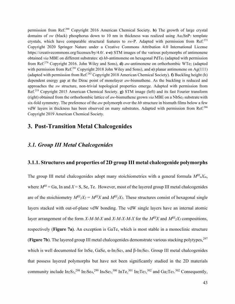
43
permission from Ref.200 Copyright 2016 American Chemical Society. b) The growth of large crystal
domains of sw (black) phosphorus down to 10 nm in thickness was realized using Au3SnP7 template
crystals, which have comparable structural features to sw-P. Adapted with permission from Ref.273
Copyright 2020 Springer Nature under a Creative Commons Attribution 4.0 International License
https://creativecommons.org/licenses/by/4.0/. c-e) STM images of the various polymorphs of antimonene
obtained via MBE on different substrates: c) hb-antimonene on hexagonal PdTe2 (adapted with permission
from Ref.276 Copyright 2016. John Wiley and Sons), d) aw-antimonene on orthorhombic WTe2 (adapted
with permission from Ref.281 Copyright 2018 John Wiley and Sons), and e) planar antimonene on Ag(111)
(adapted with permission from Ref.283 Copyright 2018 American Chemical Society). f) Buckling height (h)
dependent energy gap at the Dirac point of monolayer aw-bismuthene. As the buckling is reduced and
approaches the sw structure, non-trivial topological properties emerge. Adapted with permission from
Ref.219 Copyright 2015 American Chemical Society. g) STM image (left) and its fast Fourier transform
(right) obtained from the orthorhombic lattice of aw-bismuthene grown via MBE on a NbSe2 substrate with
six-fold symmetry. The preference of the aw polymorph over the hb structure in bismuth films below a few
vdW layers in thickness has been observed on many substrates. Adapted with permission from Ref.286
Copyright 2019 American Chemical Society.
3. Post-Transition Metal Chalcogenides
3.1. Group III Metal Chalcogenides
3.1.1. Structures and properties of 2D group III metal chalcogenide polymorphs
The group III metal chalcogenides adopt many stoichiometries with a general formula MIIInXm,
where MIII = Ga, In and X = S, Se, Te. However, most of the layered group III metal chalcogenides
are of the stoichiometry MIII2X2 = MIIIX and MIII
2X3. These structures consist of hexagonal single
layers stacked with out-of-plane vdW bonding. The vdW single layers have an internal atomic
layer arrangement of the form X-M-M-X and X-M-X-M-X for the MIIIX and MIII2X3 compositions,
respectively (Figure 7a). An exception is GaTe, which is most stable in a monoclinic structure
(Figure 7b). The layered group III metal chalcogenides demonstrate various stacking polytypes,297
which is well documented for InSe, GaSe, α-In2Se3, and β-In2Se3. Group III metal chalcogenides
that possess layered polymorphs but have not been significantly studied in the 2D materials
community include In2S3,298 In3Se4,299 In4Se3,300 InTe,301 In2Te3,302 and Ga2Te3.302 Consequently,
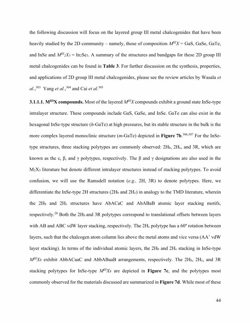
44
the following discussion will focus on the layered group III metal chalcogenides that have been
heavily studied by the 2D community – namely, those of composition MIIIX = GaS, GaSe, GaTe,
and InSe and MIII2X3 = In2Se3. A summary of the structures and bandgaps for these 2D group III
metal chalcogenides can be found in Table 3. For further discussion on the synthesis, properties,
and applications of 2D group III metal chalcogenides, please see the review articles by Wasala et
al.,303 Yang et al.,304 and Cai et al.305
3.1.1.1. MIIIX compounds. Most of the layered MIIIX compounds exhibit a ground state InSe-type
intralayer structure. These compounds include GaS, GaSe, and InSe. GaTe can also exist in the
hexagonal InSe-type structure (h-GaTe) at high pressures, but its stable structure in the bulk is the
more complex layered monoclinic structure (m-GaTe) depicted in Figure 7b.306,307 For the InSe-
type structures, three stacking polytypes are commonly observed: 2Hb, 2Hc, and 3R, which are
known as the ε, β, and γ polytypes, respectively. The β and γ designations are also used in the
M2X3 literature but denote different intralayer structures instead of stacking polytypes. To avoid
confusion, we will use the Ramsdell notation (e.g., 2H, 3R) to denote polytypes. Here, we
differentiate the InSe-type 2H structures (2Hb and 2Hc) in analogy to the TMD literature, wherein
the 2Hb and 2Hc structures have AbACaC and AbABaB atomic layer stacking motifs,
respectively.28 Both the 2Hb and 3R polytypes correspond to translational offsets between layers
with AB and ABC vdW layer stacking, respectively. The 2Hc polytype has a 60º rotation between
layers, such that the chalcogen atom column lies above the metal atoms and vice versa (AA’ vdW
layer stacking). In terms of the individual atomic layers, the 2Hb and 2Hc stacking in InSe-type
MIIIXs exhibit AbbACaaC and AbbABaaB arrangements, respectively. The 2Hb, 2Hc, and 3R
stacking polytypes for InSe-type MIIIXs are depicted in Figure 7c, and the polytypes most
commonly observed for the materials discussed are summarized in Figure 7d. While most of these
45
compounds show polytypism, GaS and h-GaTe have only been reported in the 2Hc form.308
Additionally, a first-principles calculation report by Kou et al. suggests that InSe may be stable in
other monolayer structures, although these structures have not been observed experimentally.309
Since the polymorphism in most of the MIIIXs arises from differences in stacking, the
distinction in their properties primarily results from differences in their symmetries. Both InSe-
type and m-GaTe monolayers are noncentrosymmetric. However, for the InSe-type materials,
different symmetries can be achieved via the different stacking orders in their polytypes. In
particular, the 2Hb and 3R polytypes for the InSe-type MIIIXs are noncentrosymmetric, whereas
the 2Hc stacking is centrosymmetric for even numbers of vdW layers. Since noncentrosymmetric
materials are applicable for nonlinear optics310 and anticipated to display spontaneous
polarizations,311 much attention has been directed at studying the noncentrosymmetric MIIIX
polytypes. Indeed, InSe-type monolayer MIIIXs are predicted by Li et al. to demonstrate
piezoelectricity,312 and in contrast to centrosymmetric TMDs, the 2Hb and 3R polytypes of the
InSe-type MIIIXs sustain a piezoelectric response in the multilayer form. In-plane piezoelectricity
has also been confirmed in 3R-InSe by Dai et al.313 Furthermore, SHG in the MIIIXs has been the
subject of many recent studies. Zhou et al. observed enhanced SHG in 2Hb-GaSe bilayers grown
using chemical vapor deposition (CVD) and nearly zero SHG signal in synthesized 2Hc-GaSe
bilayers.314 This result demonstrates the promise of noncentrosymmetric multilayer MIIIXs in high-
intensity SHG, which has since been confirmed experimentally in multilayer 3R-InSe315 and 2Hb-
InSe,316–318 in addition to being further investigated computationally319,320 Electronically, the 2Hb,
2Hc, and 3R polytypes of the InSe-type MIIIXs are expected to be similar.321–323 However, Sun et
al.324 calculated the carrier mobilities of 2Hc-InSe to be larger than 3R-InSe (up to ~1.5× in the
thick limit).

46
In contrast to the InSe-type monolayer structure, m-GaTe exhibits in-plane anisotropy.
Huang et al. experimentally verified the anisotropy in exfoliated 2D flakes of m-GaTe using optical
extinction and Raman spectroscopy.325 Since m-GaTe has broken inversion symmetry, it has also
been shown to exhibit SHG.326 In addition, a recent density functional theory (DFT) study by
Kosobutsky et al. suggests that m-GaTe shows a lesser degree of bandgap tunability as a function
thickness than h-GaTe.327
3.1.1.2. In2Se3. There are two monolayer structures of vdW-layered In2Se3 polymorphs – namely,
α-In2Se3 and β-In2Se3, the latter of which shares the same intralayer structure as Bi2Te3 (see section
3.3.1.1). Bulk In2Se3 also has non-layered polymorphs.328 Similar to the InSe-type MIIIX
compounds, the layered structures of In2Se3 show stacking polytypes. α-In2Se3 stacks in both the
2H and 3R polytypes, while β-In2Se3 stacks in the 1T, 2H, and 3R polytypes (Figure 7d).329,330
The 1T polytype corresponds to AA stacking where the single layers are stacked directly on top of
each other with no offset. 1T β-In2Se3 is also known as the high-temperature δ-In2Se3 phase.331 The
2H polytype for In2Se3 has an AB stacking pattern with a 60º rotation between layers, while the
3R polytype has an ABC stacking pattern with only a translational offset between the layers.
Additionally, distorted β structures, denoted as β’, have been observed for 2D In2Se3. One of the
structures reported is the result of a 1D periodic modulation along the high-symmetry
direction,332,333 and the other is a new structure with a rectangular lattice, although both are not yet
fully understood.334–336
Since the α-In2Se3 structure is noncentrosymmetric and β-In2Se3 is centrosymmetric, the
two polymorphs have significant distinctions in their properties. Firstly, α-In2Se3 is predicted to
demonstrate robust room-temperature spontaneous polarization,337 including intrinsic in-plane and
out-of-plane ferroelectricity that persists down to monolayer thickness.338 This behavior is in

47
contrast to conventional ferroelectric thin films in which the effect is supressed past a critical
thickness. Xiao et al. experimentally confirmed the room temperature out-of-plane ferroelectricity
of 2D α-In2Se3,339 while Xue et al.340 and Cui et al.341 showed the room temperature in-plane
ferroelectricity of 2D α-In2Se3. Out-of-plane and in-plane piezoelectricity have also been
experimentally confirmed in 2D α-In2Se3.342,343,313 In contrast, centrosymmetric β-In2Se3 does not
exhibit ferroelectricity or piezoelectricity. However, if the β-In2Se3 structure is distorted and the
inversion symmetry is broken, it could result in spontaneous polarizations. In particular, Zheng et
al.332 showed room temperature in-plane ferroelectricity in distorted β’-In2Se3 multilayer crystals.
In terms of electronic transport properties, Tao and Gu344 and Feng et al.345 both found β-In2Se3 to
be more conductive than α-In2Se3.
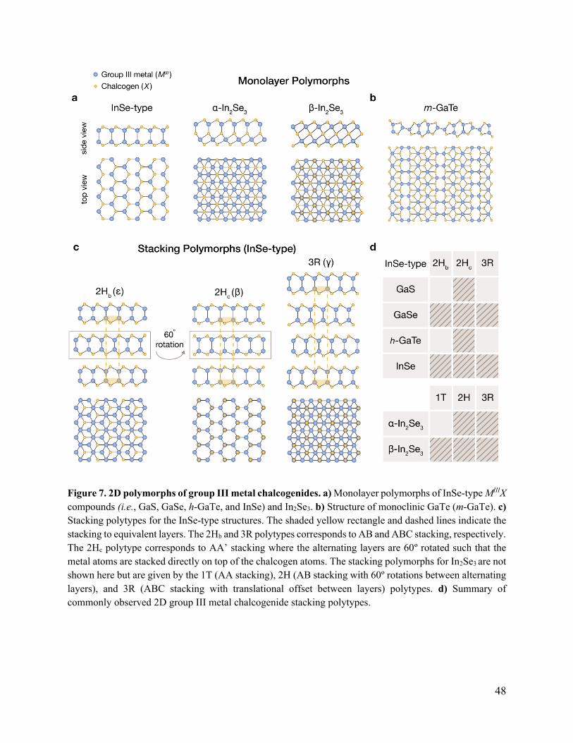
48
Figure 7. 2D polymorphs of group III metal chalcogenides. a) Monolayer polymorphs of InSe-type MIIIX
compounds (i.e., GaS, GaSe, h-GaTe, and InSe) and In2Se3. b) Structure of monoclinic GaTe (m-GaTe). c)
Stacking polytypes for the InSe-type structures. The shaded yellow rectangle and dashed lines indicate the
stacking to equivalent layers. The 2Hb and 3R polytypes corresponds to AB and ABC stacking, respectively.
The 2Hc polytype corresponds to AA’ stacking where the alternating layers are 60º rotated such that the
metal atoms are stacked directly on top of the chalcogen atoms. The stacking polymorphs for In2Se3 are not
shown here but are given by the 1T (AA stacking), 2H (AB stacking with 60º rotations between alternating
layers), and 3R (ABC stacking with translational offset between layers) polytypes. d) Summary of
commonly observed 2D group III metal chalcogenide stacking polytypes.
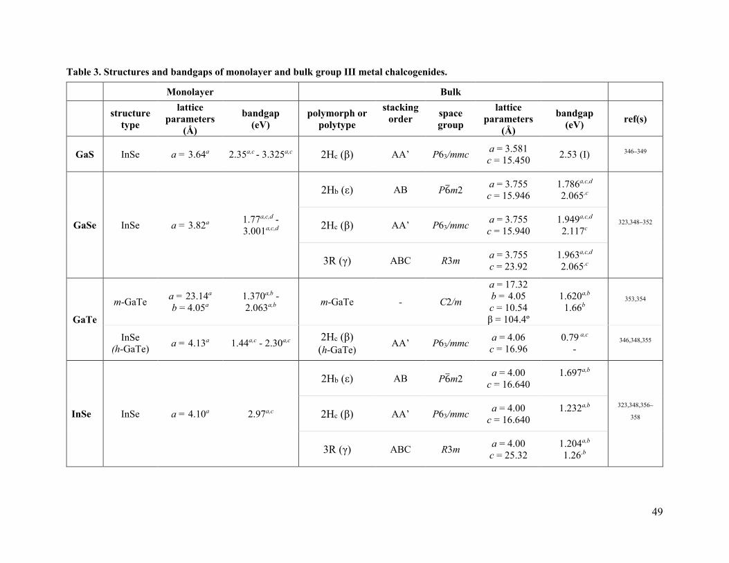
49
Table 3. Structures and bandgaps of monolayer and bulk group III metal chalcogenides.
Monolayer Bulk
structure
type
lattice
parameters
(Å)
bandgap
(eV)
polymorph or
polytype
stacking
order space
group
lattice
parameters
(Å)
bandgap
(eV) ref(s)
GaS InSe a = 3.64a 2.35a,c - 3.325a,c 2Hc (β) AA’ P63/mmc a = 3.581
c = 15.450 2.53 (I) 346–349
GaSe InSe a = 3.82a 1.77a,c,d -
3.001a,c,d
2Hb (ε) AB P6m2 a = 3.755
c = 15.946
1.786a,c,d
2.065,c
323,348–352 2Hc (β) AA’ P63/mmc a = 3.755
c = 15.940
1.949a,c,d
2.117c
3R (γ) ABC R3m a = 3.755
c = 23.92
1.963a,c,d
2.065,c
GaTe
m-GaTe a = 23.14a
b = 4.05a
1.370a,b -
2.063a,b m-GaTe - C2/m
a = 17.32
b = 4.05
c = 10.54
β = 104.4º
1.620a,b
1.66b 353,354
InSe
(h-GaTe) a = 4.13a 1.44a,c - 2.30a,c
2Hc (β)
(h-GaTe) AA’ P63/mmc
a = 4.06
c = 16.96
0.79 a,c
- 346,348,355
InSe InSe a = 4.10a 2.97a,c
2Hb (ε) AB P6m2 a = 4.00
c = 16.640
1.697a,b
323,348,356–
358 2Hc (β) AA’ P63/mmc
a = 4.00
c = 16.640
1.232a,b
3R (γ) ABC R3m a = 4.00
c = 25.32
1.204a,b
1.26,b
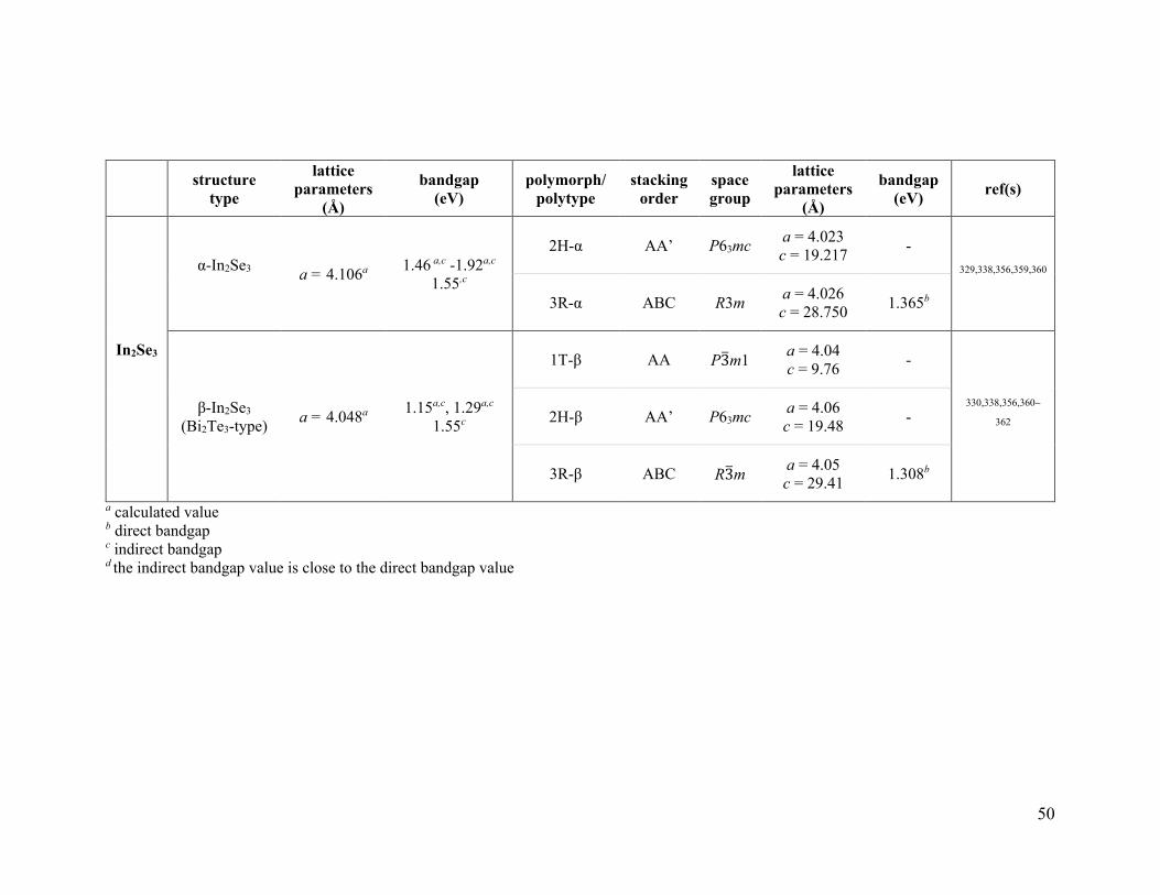
50
structure
type
lattice
parameters
(Å)
bandgap
(eV)
polymorph/
polytype
stacking
order
space
group
lattice
parameters
(Å)
bandgap
(eV) ref(s)
In2Se3
α-In2Se3
a = 4.106a
1.46 a,c -1.92a,c
1.55,c
2H-α AA’ P63mc a = 4.023
c = 19.217 -
329,338,356,359,360
3R-α ABC R3m a = 4.026
c = 28.750 1.365b
β-In2Se3
(Bi2Te3-type) a = 4.048a
1.15a,c, 1.29a,c
1.55c
1T-β AA P3m1 a = 4.04
c = 9.76 -
330,338,356,360–
362 2H-β AA’ P63mc
a = 4.06
c = 19.48 -
3R-β ABC R3m a = 4.05
c = 29.41 1.308b
a calculated value b direct bandgap c indirect bandgap d the indirect bandgap value is close to the direct bandgap value

51
3.1.2. Polymorph control of 2D group III metal chalcogenides
3.1.2.1. Synthesis conditions. Due to competing polymorphs or stoichiometries, small changes in
growth conditions can significantly affect the phase of synthesized group III metal chalcogenides.
As studied by Huang et al., the successful CVD of 2D InSe was restricted to a narrow region with
low Se sublimation temperature and high H2 content in an Ar carrier gas (Figure 8a).316 In
conditions of excess Se (from high Se sublimation temperatures) or in the absence of H2 gas, 2D
In2Se3 was formed. On the other hand, too low a concentration of Se or too high a concentration
of H2 resulted in overall poor-quality growth. For the indium-selenium system specifically, it is
common to observe the formation of different compositional phases where the reaction
temperature is one of the primary parameters used to control the phase of the deposited material.
This method of control is well illustrated by the work of Balakrishnan et al., wherein four different
phases of indium chalcogenides were obtained by varying the physical vapor deposition (PVD)
growth temperature.363 They exploited the temperature gradient of a tube furnace to obtain thick
nanoflakes of γ-In2Se3, β-In2Se3, α-In2Se3, and 3R-InSe along a substrate temperature gradient of
580 °C to 500 °C. It is important to note here that there is also an implicit precursor concentration
gradient in the PVD method used. The reaction temperature was also tuned by Hu et al. for the
chemical vapor transport (CVT) of 2D 2Hc-InSe on mica at 400 °C, while 2D α-In2Se3 was
synthesized at 450 °C.364 Both of these reports suggest a narrow temperature region in which these
various structures can be obtained and attest to the difficulty in achieving single-phase growth. In
the MBE of 2D GaSe, higher temperatures of 575 °C resulted in pure epitaxial 2Hb-GaSe on GaN,
while lower temperatures (350-450 °C) improved continuity of the films but resulted in a mixture
of 2Hb-GaSe and 2Hc-GaSe.365 This behavior is consistent with reports that the 2Hb polytype of
GaSe is more stable than 2Hc-GaSe.366 Similarly, h-GaTe is metastable367 but can be obtained

52
using PVD on mica at lower temperatures (600 °C) than the more stable m-GaTe polymorph at
760 °C.368 A mixture of the two polymorphs are obtained between these temperatures.
A recent report on the CVD of indium chalcogenides demonstrates the combination of
various parameters for specific polymorphs. Using a high temperature of 850 °C for the In source
(In2O3) and 750 °C for the substrate, Liu et al. obtained nanoscale structures of 2H α-In2Se3 on
SiO2 for upstream substrate positions and γ-In2Se3 when the substrate was positioned further
downstream.330 By decreasing the temperature of both the In2O3 and substrate by ~100 °C, 1T β-
In2Se3 was synthesized. On the other hand, switching the substrate to HOPG under those same
conditions resulted in 2H β-In2Se3. Overall, precise level of control over these In2Se3 polymorphs
is difficult to achieve. As demonstrated by Figure 8b, CVD of In2Se3 on SiO2 can result in a
mixture of 1T β-In2Se3, 3R β-In2Se3, and 2H α-In2Se3.
The cooling rate of materials grown at elevated temperatures presents another parameter
for controlling the ultimate structure of 2D MIIInXm crystals. In a report on the CVD of 2D In2Se3
by Cui et al., slow cooling (0.1 °C/min) favored the formation of α-In2Se3 over β-In2Se3.341 Crystals
synthesized with fast cooling were instead dominated by β-In2Se3. This result is consistent with
previous accounts of bulk β-In2Se3 as a high-temperature phase of α-In2Se3 that reverts back to
bulk α-In2Se3 upon cooling.369 In combination with a 2D thickness effect (section 3.1.2.3),344
quenching may help to isolate the high-temperature form at room temperature. In another report,
Lin et al. observed that slow cooling rates (< 5°C/min ) following PVD resulted in α-In2Se3 while
fast cooling rates (>100 °C/min) resulted in a In2Se3 superlattice phase.370
3.1.2.2. Substrates. The choice of substrate in the growth of 2D MIIInXm crystals has been shown
to affect the synthesized structure. By using c-plane sapphire and Si(111) as substrates in the metal-
organic CVD (MOCVD) of In2Se3, Zhang et al. obtained epitaxial 2D β-In2Se3.371 In contrast, the

53
use of amorphous SiO2 resulted in nonlayered γ-In2Se3. Similarly, Bae et al. attributed the MBE-
growth of h-GaTe on GaAs(001) to a better match in symmetry to the GaAs(001) surface than the
m-GaTe polymorph.372 However, upon further GaTe deposition, the additional growth was
monoclinic, presumably due to relaxation of the structure into its more stable form as the epitaxial
strain near the interface with the GaAs substrate diminished. Despite the existence of a quasi vdW
gap, Yonezawa et al. reported a GaSe film with an alternative structure to the expected InSe-type
structure (also referred to as ‘wurtzite-like’).373 Instead, the GaSe layers near the interface with a
Ge(111) substrate showed a zinc blende-like structure where the top and bottom Ga-Se bonds point
in opposite directions. The authors thus make the case that despite the vdW gap, the substrate can
still significantly influence the structure of the deposited 2D material. Structural preferences are
also affected by substrate pre-treatments. As reported by Diep et al., the MBE growth of GaSe
films on GaAs(001) favored 2Hb-GaSe, whereas growth on Se-terminated GaAs(001) resulted in
2Hc-GaSe.374
3.1.2.3. Post-synthesis processing. The processing of 2D group III metal chalcogenides after
synthesis is a frequently used method of phase conversion. In particular, thermal annealing is a
prevalent way to transform one 2D group III metal chalcogenide into another. Tao and Gu
converted exfoliated 2D α-In2Se3 into β-In2Se3 by annealing the flakes in argon at 533-633 K,
depending on the flake thickness.344 The authors also observed a superlattice with the conversion
to β-In2Se3, as has also been observed for other reports of 2D β-In2Se3.335 Furthermore, a dramatic
decrease in resistivity is accompanied with the conversion into β-In2Se3. This result was
corroborated by Feng et al.345 who followed the same procedure to obtain higher field-effect
mobilities (18× greater to 22.8 cm2V-1s-1) and better photodetector performance from multilayer
β-In2Se3 flakes that were thermally converted from α-In2Se3. A favorable increase in current was
54
observed, but the Ion/Ioff ratio was severely compromised due to metallic behavior. Interestingly,
this behavior was also observed by Feng et al. in annealed 2D 2Hc-InSe.375 In their report, an
exfoliated 2Hc-InSe flake was annealed at 573 K in an H2/argon reducing atmosphere, and the
annealed crystal demonstrated an increased mobility (4× greater to 299.1 cm2V-1s-1) and
photoresponsivity, but orders of magnitude lower Ion/Ioff ratio. The authors determined the effect
to be the result of the formation of an InSe superlattice. In contrast, a prior report by Osman et al.
on annealed 2D 2Hc-InSe found degradation of mobility (4× reduced from 10.32 cm2V-1s-1 to 2.37
cm2V-1s-1) and photodetector performance after thermal processing.376 In that case, the exfoliated
2Hc-InSe was annealed at 200-400 °C in an argon atmosphere without H2, which resulted in partial
conversion of the crystals to γ-In2Se3. Thermally induced phase transitions can also be monitored
using the SHG signal intensity as has been demonstrated for the conversion of noncentrosymmetric
α-In2Se3 to centrosymmetric β-In2Se3. Xue et al. observed a loss of SHG intensity after annealing
an exfoliated α-In2Se3 crystal to 573 K,340 and Xiao et al. observed the dramatic decrease of SHG
signal intensity during annealing of a 4-layer thick exfoliated α-In2Se3 crystal to 700 K (which is
presumably due to a transition to β-In2Se3).339 In addition to thermal annealing, laser annealing can
be used to induce a phase transformation and holds the considerable advantage of patternable
conversion. As shown in Figure 8c, Yu et al. demonstrated this concept using a femtosecond laser
to partially convert h-GaTe into m-GaTe,368 which is the more stable polymorph.367
Cooling can also lead to structural phase transitions in the 2D group III metal chalcogenides. Zhang
et al. recently reported the reversible phase conversion between β-In2Se3 at room temperature and
a distorted β’ In2Se3 structure at 77 K.335 As shown in the STM images of Figure 8d, the hexagonal
lattice of β-In2Se3 transformed to a rectangular lattice at low temperatures. The hexagonal lattice
is recovered upon warming to room temperature. A subsequent report by Dong et al. on β-In2Se3
55
grown on WS2 demonstrated the existence of a thickness dependence for this phenomenon,336 with
the transition temperature increasing with an increasing number of layers.
While the application of hydrostatic pressure is a commonly employed method to control
polymorphism in bulk group III metal chalcogenides, relatively few reports use pressure as a
structural tuning parameter for the 2D group III metal chalcogenides. Su et al. recently used
hydrostatic pressure to alter the symmetry of 2Hb-InSe.377 They observed a continuous transition
from three-fold symmetry to mirror symmetry as a hydrostatic pressure of up to 8.2 GPa was
applied. The symmetry was monitored via the polarization of the SHG signal from the 2D 2Hb-
InSe sample and was found to be reversible upon return to atmospheric pressure. Su et al. attributed
the change in symmetry to sliding of adjacent vdW layers under pressure.
The application of an electric current has also been shown to control In2Se3 polymorphs. Choi et
al. demonstrated the reversible electrically-driven conversion between β-In2Se3 and γ-In2Se3.378
This transformation is mediated by Joule heating from the applied current, which is consistent with
the previous understanding of γ-In2Se3 as a higher temperature phase compared to β-In2Se3.369
Starting with an exfoliated α-In2Se3 crystal, the device was annealed to 250 °C to convert the
crystal to β-In2Se3. Pulses of 3 V and 0.7 V were then used to RESET or SET the device into its
high (γ-In2Se3) or low (β-In2Se3) resistance states, respectively. Lastly, a report by Kou et al.
suggests that charge doping, such as through electron injection or alkali metal adsorption, can be
used to stabilize yet unrealized polymorphs of InSe with different intralayer structures.309
3.1.2.3. Thickness. Another factor in the polymorph control of 2D group III metal chalcogenides
is the thickness of the material. Upon exfoliation of bulk m-GaTe crystals, Zhao et al. observed its
spontaneous transformation into h-GaTe.379 As shown in Figure 8e, the selected area electron
diffraction (SAED) patterns of bulk GaTe and exfoliated 2D GaTe were of a monoclinic and
56
hexagonal lattice, respectively. The transformation occurred below a critical thickness of 4 layers.
The authors performed first-principles calculations, which supported the explanation that the
transformation occurred due to the balance between the interlayer interactions and surface energy
shifting toward h-GaTe as the surface energy contribution becomes more dominant in thinner
layers. Furthermore, nanoscale thicknesses in In2Se3 have been found to stabilize the β-In2Se3
polymorph at room temperature.344,345 In the bulk, the high-temperature β-In2Se3 phase normally
reverts back into α-In2Se3 at room temperature,369 but a study by Tao and Gu suggests that the
nanoscale thickness of the crystal may stabilize the metastable phase at room temperature. The
authors observed that the annealing temperature required for the phase transformation
demonstrated a clear thickness dependence with higher temperatures required for thinner crystals.
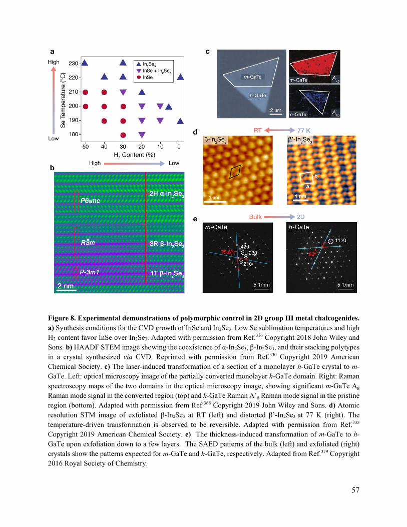
57
Figure 8. Experimental demonstrations of polymorphic control in 2D group III metal chalcogenides.
a) Synthesis conditions for the CVD growth of InSe and In2Se3. Low Se sublimation temperatures and high
H2 content favor InSe over In2Se3. Adapted with permission from Ref.316 Copyright 2018 John Wiley and
Sons. b) HAADF STEM image showing the coexistence of α-In2Se3, β-In2Se3, and their stacking polytypes
in a crystal synthesized via CVD. Reprinted with permission from Ref.330 Copyright 2019 American
Chemical Society. c) The laser-induced transformation of a section of a monolayer h-GaTe crystal to m-
GaTe. Left: optical microscopy image of the partially converted monolayer h-GaTe domain. Right: Raman
spectroscopy maps of the two domains in the optical microscopy image, showing significant m-GaTe Ag
Raman mode signal in the converted region (top) and h-GaTe Raman A’g Raman mode signal in the pristine
region (bottom). Adapted with permission from Ref.368 Copyright 2019 John Wiley and Sons. d) Atomic
resolution STM image of exfoliated β-In2Se3 at RT (left) and distorted β’-In2Se3 at 77 K (right). The
temperature-driven transformation is observed to be reversible. Adapted with permission from Ref.335
Copyright 2019 American Chemical Society. e) The thickness-induced transformation of m-GaTe to h-
GaTe upon exfoliation down to a few layers. The SAED patterns of the bulk (left) and exfoliated (right)
crystals show the patterns expected for m-GaTe and h-GaTe, respectively. Adapted from Ref.379 Copyright
2016 Royal Society of Chemistry.

58
3.2. Group IV Metal Chalcogenides
3.2.1. Structures and properties of 2D group IV metal chalcogenide polymorphs
The layered group IV metal chalcogenides primarily exist in two compositions: MIVX and MIVX2,
where MIV = Ge, Sn and X = S, Se, Te. In contrast to the group III metal chalcogenides, the group
IV metal chalcogenides have relatively simple binary phase diagrams, which implies that the MIVX
and MIVX2 stoichiometries dominate the stable binary compositions.380,381 However, the
polytypism exhibited by the MIVX2s creates a rich phase space,382–385 although this range of
structures is relatively underexplored in the 2D literature. In addition to the MIVX and MIVX2
stoichiometries, the existence of layered Ga4Se9 has been reported.386 Silicon chalcogenides are
seldom studied, ambient unstable, and generally do not form layered structures.387 The exception
is Si2Te3, which crystallizes in a layered structure belonging to the P31c space group.388 The
existence and structures of other silicon tellurides remain controversial.389,390 Lead chalcogenides
also do not form layered structures in the bulk.391 The following discussion will focus on the stable
2D materials of MIVX = GeS, GeSe, GeTe, SnS, SnSe, SnTe and MIVX2 = GeS2, GeSe2, SnS2,
SnSe2. A summary of the structures and bandgaps for these group IV metal chalcogenides is
provided in Table 4. For further discussions on the synthesis, properties, and applications of 2D
group IV metal chalcogenides, please see the review articles by Xia et al.,392 Hu et al.,393 and
Boschker et al.394
3.2.1.1. MX compounds. For the monochalcogenides of GeS, GeSe, SnS, and SnSe, the most
stable polymorph in ambient conditions is a vdW-layered GeS-type orthorhombic structure of the
space group Pnma, which is known as the α phase of the aforementioned compounds.383 The
corresponding monolayer structure is the asymmetric washboard (aw) structure (Figure 9a). This

59
structure was calculated to be the most stable monolayer configuration for 2D GeS, GeSe, SnS,
and SnSe.395,396 While bulk SnTe exists in a cubic NaCl-type structure (space group Fm3m) at
ambient conditions (β-SnTe),383 it transforms into the Pnma (aw) structure at high pressures (γ-
SnTe).397 In the 2D limit, the aw structure was predicted to be stable for SnTe395 and was confirmed
experimentally in ultrathin films grown using MBE.398 Bulk GeTe crystallizes in an R3m
rhombohedral structure at ambient conditions (α-GeTe), which corresponds to a distorted NaCl
structure that is also known as the A7 structure (Strukturbericht designation).399,400 The A7
structure is similarly adopted by several group V elemental materials (section 2.3.1) and is shared
by the low-temperature (< 100 K) SnTe phase (α-SnTe). The corresponding monolayer structure
is the hexagonal buckled (hb) structure (Figure 9a). Moreover, the hb structure has been predicted
to be stable for monolayer GeTe in a study by Li et al.,401 and has been observed experimentally
for both ultrathin GeTe and SnTe. The aw structure has also been predicted to be stable for
GeTe,395,402 but has yet to be observed. While bulk A7 (hb) GeTe displays short in-plane bonds
and long out-of-plane bonds for a layered-like structure, it is not truly vdW bonded.403 It should
also be noted that for low-temperature bulk A7 (hb) SnTe, the rhombohedral distortion is much
smaller than in GeTe, such that its lattice parameters are very close to its room temperature NaCl-
type structure (β-SnTe), which is not vdW bonded in the out-of-plane direction.404
A summary of the structures observed in the group IV metal monochalcogenides is
presented in Figure 9b. Many additional monolayer structures have been proposed but remain to
be confirmed experimentally.405–411,396,412 The stacking order in 2D MIVXs is predicted to affect
their properties,413–416 but the observation of polytypic variation is not well documented in contrast
to the MIVX2 compounds that show a variety of polytypes. The monolayer aw and hb structures of
the MIVXs are the same as the aw and hb structures observed in the group V elemental 2D materials
60
(e.g., phosphorene, bismuthene), except that the atoms alternate between the metal and chalcogen.
Similarly, these compounds have 10 electrons for each atom pair. As a result, the MIVXs are known
as analogues and isoelectronic counterparts to phosphorene and other group V elementals.405,417
In contrast to the hb structure, the aw monolayer demonstrates in-plane anisotropy,418–422
including anisotropic spin-orbit splitting of the bands for applications in spin-transport devices.423
Among the 2D aw MIVX compounds, GeS shows the greatest degree of in-plane anisotropy in its
properties.419,424,425 The 2D aw MIVX compounds are predicted to have large piezoelectric
coefficients exceeding those of other 2D vdW materials due to their noncentrosymmetric structure
in tandem with their flexibility along the armchair direction, which is the main polar direction. The
2D aw MIVX compounds are also predicted to be multiferroic, exhibiting both ferroelectricity and
ferroelasticity.426,427 Additionally, Wang et al. predicted large SHG susceptibility in these
multiferroic compounds.428 The first observation of 2D in-plane ferroelectricity was reported by
Chang et al. in ultrathin aw-SnTe.429 The Curie temperature was found to be much higher than in
bulk SnTe, owing to the orthorhombic structure.398 In-plane ferroelectricity, along with SHG, was
also recently confirmed in ultrathin SnS by Bao et al.430 However, due to the vdW layer stacking
arrangement, even-numbered layers of the aw SnS structure, as well as the bulk form, are
centrosymmetric with no net polarization or SHG. The bulk forms of other aw MIVX compounds
are also centrosymmetric. Lastly, the lone electron pairs of the puckered aw structure are believed
to be responsible for the difficulty in exfoliating and synthesizing single layers of these
crystals.431,432
Since the rhombohedral distortion in the hb structure also results in a noncentrosymmetric
structure, α-GeTe is well known as a ferroelectric material, including in the nanoscale limit.433,434
Furthermore, GeTe is a phase change material with a sharp contrast in properties associated with
61
an amorphous to crystalline transition. This contrast is due to the presence of resonant bonding in
the crystalline phase, although this bonding character is weakened by the rhombohedral distortion.
This nuance to the GeTe bonding character imparts a high degree of electronic polarizability.399
Although not as well studied, some characteristics of resonant bonding also exist in SnTe.435 For
2D SnTe, the implications of the aw versus hb structure for its ferroelectric behavior was
investigated by Kaloni et al.436 In particular, they observed antiferroelectric coupling in ultrathin
SnTe layers (< 6 layers), which converted to ferroelectric coupling with an increasing number of
layers due to a transition from an orthorhombic (aw) to rhombohedral structure (hb). Furthermore,
the cubic polymorph of SnTe was experimentally shown to be a topological crystalline insulator
by Tanaka et al.437 The authors suggested that despite the small rhombohedral distortion in hb-
SnTe, which breaks the symmetry of one of the two mirror planes, it could also be a topological
crystalline insulator.
3.2.1.2. MIVX2 compounds. For the MIVX2 compounds, two types of monolayer structures have
been observed. The two germanium dichalcogenides (GeS2 and GeSe2) crystallize in the layered
monoclinic m-GeS2 structure,438,439 whereas the tin dichalcogenides (SnS2 and SnSe2) instead form
a CdI2-type structure. The two structures are depicted in Figure 9a and summarized in Figure 9c.
The monoclinic m-GeS2-type structure is known as the β phase for both GeS2 and GeSe2 since it
is a high-temperature modification, although it is stable at ambient conditions.440,441 Additionally,
GeS2 and GeSe2 exhibit other polymorphs (some layered) at different pressures and temperatures,
but these structures are not yet studied in the 2D literature. Specifically, GeS2 exhibits another
monoclinic low-temperature structure with space group Pc,442 not to be confused with the m-GeS2
structure (space group P21/c) referred to here. The m-GeS2 structure is anisotropic443 and was
shown by Yang et al. to have relatively weak interlayer coupling.444 Calculations by Yan et al.
62
also found a nearly layer-independent bandgap in 2D GeSe2 with experimental investigations
revealing an anisotropic optical response.445
The CdI2-type structure of SnS2 and SnSe2 is sometimes referred to as the 1T structure in
the 2D literature, as derived from the TMDs.446 The most common multilayer polytype for SnS2
and SnSe2 is 1T, although a plethora of other stacking polytypes exist in the bulk.447–449 In a
computation study by Seminovski et al., the 1T polytype in SnS2 was found to have a slightly
larger indirect bandgap than the other common 2H polytype.450 It should be noted that many texts
refer to the 1T and 2H polytypes for SnS2 and SnSe2 as ‘2H’ and ‘4H’, respectively, in reference
to the arrangement of M-X atomic layers within the vdW layer.29 Hence, when reviewing the
literature, it is helpful to refer to the lattice parameters for polytype clarity. In contrast to the m-
GeS2 structure, 2D SnS2 and SnSe2 are predicted to exhibit stronger interlayer coupling, as well as
excitonic effects.451 Additionally, superconductivity has been reported when 2D SnSe2 was
interfaced with graphene452 or SrTiO3,453 gated by an electric-double-layer,454 or intercalated with
lithium compounds.455
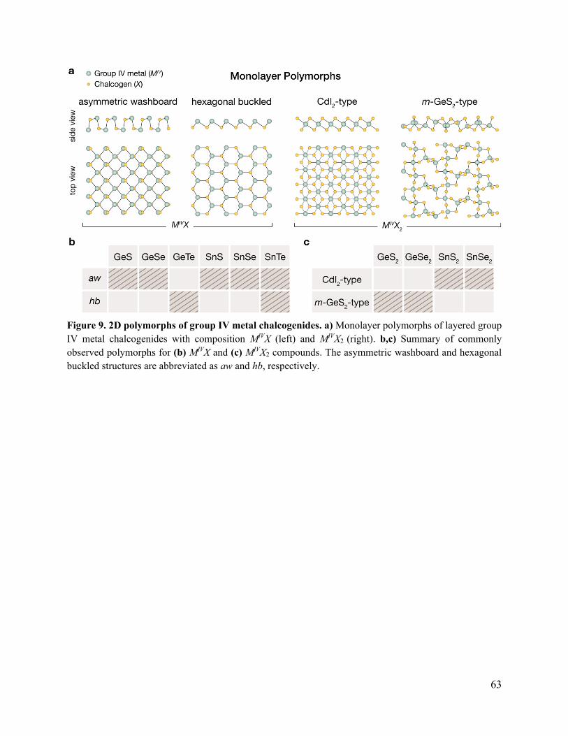
63
Figure 9. 2D polymorphs of group IV metal chalcogenides. a) Monolayer polymorphs of layered group
IV metal chalcogenides with composition MIVX (left) and MIVX2 (right). b,c) Summary of commonly
observed polymorphs for (b) MIVX and (c) MIVX2 compounds. The asymmetric washboard and hexagonal
buckled structures are abbreviated as aw and hb, respectively.

64
Table 4. Structures and bandgaps of monolayer and bulk group IV metal chalcogenides.
Monolayer Bulk
structure
type
lattice
parameters
(Å)
bandgap
(eV) name
structure
type
space
group
lattice
parameters
(Å)
bandgap
(eV) ref(s)
GeS aw a = 4.40a,g
b =3.68a,g 1.69 - 2.32a,c α-GeS GeS Pnma
a = 4.30
b = 3.64
c = 10.47
1.54 - 1.8d 417,456
GeSe aw a = 4.26a,g
b = 3.99a,g 1.14 - 1.54a,b α-GeSe GeS Pnma
a = 4.39
b = 3.83
c = 10.83
1.14c,d 417,457
GeTe hb a = 3.96a 2.35 a,c α-GeTe A7 R3m a = 4.156
c = 10.663 0.3 - 0.8b 401,458,459
SnS aw a = 4.24a,g
b = 4.07a,g 1.40 - 1.96a,c,d α-SnS GeS Pnma
a = 4.334
b = 3.987
c = 11.20
1.07 - 1.18c,d 417,456
SnSe aw a = 4.36a,g
b = 4.30a,g 1.01 - 1.44a,c,d α-SnSe GeS Pnma
a = 4.445
b = 4.153
c = 11.501
0.96c 417,460,461
SnTe
aw a = 4.57a
b = 4.56a 0.70 - 1.02a,c γ-SnTe GeS Pnma
a = 4.48 b
b = 4.37b
c = 11.59b
0.3a,c,e 418,462,463
hb - - α-SnTe A7 R3m a = 6.33c
c = 6.33c - 404,464
GeS2 m-GeS2 - - β-GeS2 m-GeS2 P21/c
a = 6.720
b = 16.101
c = 11.436
β = 90.88º
3.65 b 438,443
GeSe2 m-GeS2 a = 7.104a
b = 17.095a 2.96b β-GeSe2 m-GeS2 P21/c
a = 7.016
b = 16.796
c = 11.831
β = 90.65º
2.7b 439,445,465
SnS2 CdI2
(1T monolayer) a = 3.68a 2.41a,c
2.34c 1T-SnS2 CdI2 (1T) P3m1
a = 3.64
c = 5.88 2.06c, 2.157c 451,466–468
SnSe2 CdI2
(1T monolayer) a = 3.83a
1.69a,c
1.8c on graphene 1T-SnSe2 CdI2 (1T) P3m1
a = 3.81
c = 6.14 1.02c 451,452,467,468

65
a calculated value b direct bandgap c indirect bandgap d the indirect bandgap value is close to the direct bandgap value e Obtained at high pressure f The rhombohedral distortion is small enough to approach a cubic structure gA structural transition to a square lattice (a = b) is predicted above certain temperatures469–471

66
3.2.2. Polymorph control of 2D group IV metal chalcogenides
The following discussion reviews recent efforts toward controlling the structure of 2D group IV
metal chalcogenides. For the sake of experimental clarity, MIVX and MIVX2 compounds will be
discussed together despite not being polymorphs of each other. For example, while SnS and SnS2 are
considered different chemical entities, the synthesis of 2D SnS is intimately related to the synthesis
of 2D SnS2 and are thus reviewed together.
3.2.2.1. Synthesis conditions. Most demonstrations of phase control in 2D group IV metal
chalcogenides are based on manipulating the synthesis conditions. Firstly, the synthesis
temperature in the CVD of 2D group IV metal chalcogenides is a crucial parameter in determining
the resulting phase. Mutlu et al. used SnO2 and S powders for the CVD of 2D tin chalcogenides
and found that SnS2 grows at lower temperatures of ~425 ºC, whereas SnS forms at a higher
temperature of ~550 ºC.472 Huang et al. observed a similar phenomenon in the CVD growth of
SnSe and SnSe2,473 where 2D SnSe2 was formed at ~430-470 ºC, whereas SnSe was formed at
~510 ºC. Both of these results are in agreement a previous study on the CVT of bulk tin
chalcogenides wherein SnS grew at high temperature, SnS2 at medium temperatures, and non-
layered Sn2Se3 at low temperatures.474 Additionally, a precursor concentration gradient can give
rise to a variety of phases. Li et al. observed the presence of 2D nanocrystals of SnS, SnS2 on top
of SnS, and SnS2 on mica substrates positioned from upstream (SnS) to downstream (SnS2).475
Since the temperature of the substrates was comparable, the authors attributed this phase evolution
to the decreasing SnS:S vapor concentration from upstream (excess SnS) to downstream (excess
S), although the exact precursor concentration ratios were not quantified. This concept was also
corroborated in a study by Wang and Pang where thick SnSe or SnSe2 flakes were obtained
depending on the Se:SnO2 precursor powder loading ratio.476 SnSe was synthesized at a precursor
67
loading of 50 mg Se:20 mg SnO2, and SnSe2 was synthesized at a loading of 300 mg Se:20 mg
SnO2. A report by Zhang et al. mapped the phase of the synthesized 2D tin sulfide as a function of
the CVD precursor concentration and temperature (Figure 10a).477 In agreement with the
previously mentioned accounts, the formation of SnS was favored at high temperatures, whereas
SnS2 was favored at lower temperatures. Counterintuitively, the relative increase of the sulfur
precursor (H2S) to the tin precursor (SnCl4) favored the formation of SnS. After further
investigation, this effect was found to be due to the reduction of SnS2 into SnS by H2 gas formed
from the decomposition of the H2S precursor. Thus, increased H2S concentration resulted in
increased H2 concentration for the reduction of SnS2 into SnS, enabling the deposition of SnS at
even lower temperatures. This mechanism is in agreement with a previous report for the CVD of
tin chalcogenide nanoflakes by Ahn et al.478 The authors reported that SnS could be grown instead
of SnS2 at reaction temperatures of 620-680 ºC when H2 was added to the N2 carrier gas. When
pure N2 carrier gas was used, SnS2 was synthesized. The structure of 2D SnTe can also be tuned
via the reaction temperature. As shown in Figure 10b, Chang et al. observed higher percentages
of aw-SnTe coverage on graphene with higher growth temperatures and low thicknesses.479 At
thicknesses greater than 8 vdW layers, either the cubic or hb-SnTe structure is favored (depending
on the temperature of the measurement). This observation is in agreement with previous
calculations by Chang et al., which determined the aw phase to be more stable than hb at low
thicknesses.
Notably, the aforementioned accounts of phase control in the synthesis of 2D group IV
metal chalcogenides are concentrated on tin chalcogenides. With the exception of a recent report
by Sutter et al., in which a bulk Ge surface was sulfurized to form GeS and GeS2,480 phase control
68
of 2D germanium chalcogenides is limited, which may be due to the generally limited number of
reports on the vapor-phase synthesis of 2D germanium chalcogenides.
3.2.2.2. Substrates. The role of the substrate in the structure of MBE-grown ultrathin GeTe films
was recently studied. In particular, the growth of 2D GeTe films initiated as an amorphous layer
on Si(111)-(7 x7) and Si(111)-(1 x 1)-H instead of crystalline hb-GeTe.481,482 A study by Wang et
al. revealed the spontaneous crystallization of GeTe films into hb-GeTe after a critical thickness
of 4 layers when deposited on Si(111)-(1 x 1)-H.482 The authors attributed this phenomenon to the
emergence of resonant bonding, which their simulations suggested could only take place above a
critical thickness. In contrast, the immediate crystallization of ultrathin GeTe was observed for
deposition on Sb-terminated Si(111).483 However, the periodicity in the initial layers was slightly
larger than expected for hb-GeTe. The authors suggested that this alternate phase in GeTe films
below 2 layers is either the cubic (without rhombohedral distortion) high-temperature structure of
GeTe or is the result of disorder in the bonding. Hilmi et al. recently investigated the MBE growth
of 2D GeTe on Sb2Te3-buffered Si(111) and also found an immediately crystalline hb-GeTe
ultrathin film.484 Furthermore, the Sb2Te3-buffered substrate enabled the formation of crystalline
films at lower substrate temperatures than Si(111), which is supported by a previous study by
Simpson et al.485 The authors also observed lower GeTe post-deposition crystallization
temperatures using Sb2Te3 substrates. For the formation of aw-SnTe, the role of the substrate is
still unclear since all reports on 2D aw-SnTe have thus far only used epitaxial graphene on silicon
carbide.398,429,436,479 Additionally, the use of confined epitaxy was recently reported to achieve 2D
GeTe2. GeTe2 is a metastable structure that has not been observed in the bulk due to its
decomposition into GeTe and Te.486 However, Wang et al. reported the formation of a monolayer
of CdI2-type GeTe2 by templating its growth in a matrix of Te-rich GeSb2Te4.487 Hence, the use of
69
substrates and their ability to template or apply strain to 2D materials may enable access to
metastable structures.
3.2.2.3. Post-synthesis processing. The conversion of group IV metal chalcogenides from one
structure into another has been demonstrated using thermal and irradiation processes. Zhou et al.
converted SnS2/graphene nanocomposites grown using hydrothermal synthesis into SnS/graphene
nanocomposites using a 600 ºC annealing step in a tube furnace with argon gas flow.488 The
proposed mechanism is the loss of sulfur during the annealing. This mechanism is supported by
the findings of Tian et al.,489 shown in Figure 10c,d. In their report, a mechanically exfoliated 2D
CdI2-type SnSe2 crystal is partially converted into aw-SnSe by vacuum annealing in a tube furnace
at 300 ºC. The partial conversion is achieved by encapsulating a section of the SnSe2 crystal with
exfoliated hBN. As verified by Raman spectroscopy, the encapsulated area remained as SnSe2,
while the exposed region was converted to SnSe and accompanied by a reduction in thickness of
~4 nm. The implied mechanism of the SnSe2 phase preservation is thus the prevention of selenium
loss. The reverse conversion of 2D SnS into SnS2 has been demonstrated by Sutter et al. using
thermal annealing in excess sulfur.490 The authors used a Knudsen cell to evaporate SnS powder
and deposit 2D SnS domains on a bulk SnS2 crystal substrate in UHV. At both higher and lower
substrate temperatures than ~300 ºC, only SnS deposition was observed. However, at
approximately 300 ºC, the conversion of deposited SnS domains into SnS2 was observed, resulting
in 2D SnS2 with a twisted orientation with respect to the original SnS2 substrate (Figure 10e,f).
The authors suggested that this conversion can be attributed to the availability of excess sulfur
from both the SnS2 substrate and single sulfur species from the SnS powder source at temperatures
of ~300 ºC. They support this explanation by demonstrating the conversion of 2D SnS crystals
deposited on MoS2 into 2D SnS2 crystals following post-annealing in a tube furnace in the presence
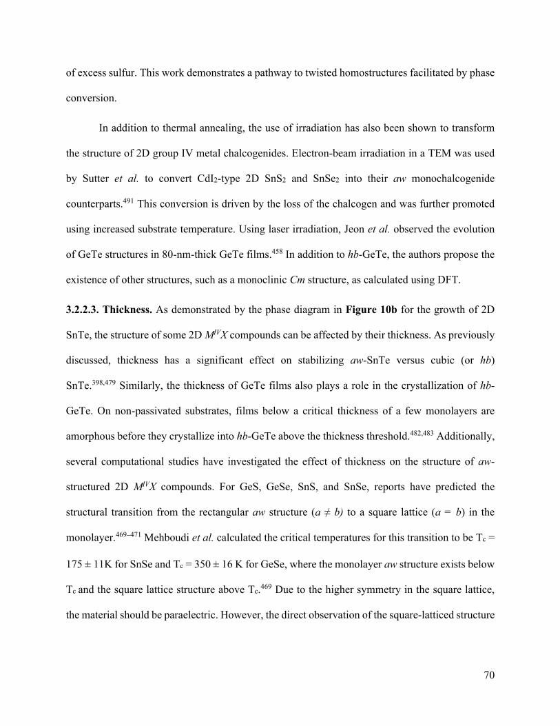
70
of excess sulfur. This work demonstrates a pathway to twisted homostructures facilitated by phase
conversion.
In addition to thermal annealing, the use of irradiation has also been shown to transform
the structure of 2D group IV metal chalcogenides. Electron-beam irradiation in a TEM was used
by Sutter et al. to convert CdI2-type 2D SnS2 and SnSe2 into their aw monochalcogenide
counterparts.491 This conversion is driven by the loss of the chalcogen and was further promoted
using increased substrate temperature. Using laser irradiation, Jeon et al. observed the evolution
of GeTe structures in 80-nm-thick GeTe films.458 In addition to hb-GeTe, the authors propose the
existence of other structures, such as a monoclinic Cm structure, as calculated using DFT.
3.2.2.3. Thickness. As demonstrated by the phase diagram in Figure 10b for the growth of 2D
SnTe, the structure of some 2D MIVX compounds can be affected by their thickness. As previously
discussed, thickness has a significant effect on stabilizing aw-SnTe versus cubic (or hb)
SnTe.398,479 Similarly, the thickness of GeTe films also plays a role in the crystallization of hb-
GeTe. On non-passivated substrates, films below a critical thickness of a few monolayers are
amorphous before they crystallize into hb-GeTe above the thickness threshold.482,483 Additionally,
several computational studies have investigated the effect of thickness on the structure of aw-
structured 2D MIVX compounds. For GeS, GeSe, SnS, and SnSe, reports have predicted the
structural transition from the rectangular aw structure (a ≠ b) to a square lattice (a = b) in the
monolayer.469–471 Mehboudi et al. calculated the critical temperatures for this transition to be Tc =
175 ± 11K for SnSe and Tc = 350 ± 16 K for GeSe, where the monolayer aw structure exists below
Tc and the square lattice structure above Tc.469 Due to the higher symmetry in the square lattice,
the material should be paraelectric. However, the direct observation of the square-latticed structure
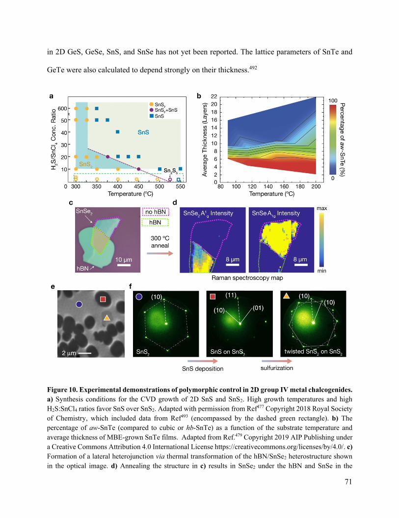
71
in 2D GeS, GeSe, SnS, and SnSe has not yet been reported. The lattice parameters of SnTe and
GeTe were also calculated to depend strongly on their thickness.492
Figure 10. Experimental demonstrations of polymorphic control in 2D group IV metal chalcogenides.
a) Synthesis conditions for the CVD growth of 2D SnS and SnS2. High growth temperatures and high
H2S:SnCl4 ratios favor SnS over SnS2. Adapted with permission from Ref477 Copyright 2018 Royal Society
of Chemistry, which included data from Ref493 (encompassed by the dashed green rectangle). b) The
percentage of aw-SnTe (compared to cubic or hb-SnTe) as a function of the substrate temperature and
average thickness of MBE-grown SnTe films. Adapted from Ref.479 Copyright 2019 AIP Publishing under
a Creative Commons Attribution 4.0 International License https://creativecommons.org/licenses/by/4.0/. c)
Formation of a lateral heterojunction via thermal transformation of the hBN/SnSe2 heterostructure shown
in the optical image. d) Annealing the structure in c) results in SnSe2 under the hBN and SnSe in the
72
unencapsulated region, as evidenced by the Raman maps showing significant SnSe2 A1g Raman peak
intensity under the hBN (left) and significant SnSe A1g Raman peak intensity in the unencapsulated region
(right). Adapted with permission from Ref.489 Copyright 2018 American Chemical Society. e) Low-energy
electron microscopy (LEEM) image showing the deposition of SnS (red square) and twisted-SnS2 (yellow
triangle) on the SnS2 substrate (blue circle). f) Micro low-energy electron diffraction (LEED) of the
hexagonal single crystal SnS2 substrate (left), orthorhombic SnS islands upon SnS deposition (center), and
a twisted hexagonal SnS2 domain from sulfurization of deposited SnS (right). The sulfurization occurs from
further SnS deposition at a temperature of ~300 ºC. Adapted from Ref.490 Copyright 2019 Springer Nature
under a Creative Commons Attribution 4.0 International License
https://creativecommons.org/licenses/by/4.0/.
3.3. Group V Metal Chalcogenides
3.3.1. Structures and properties of 2D group V metal chalcogenide polymorphs
Layered vdW group V metal chalcogenides mostly exist in the composition MV2X3, where MV =
As, Sb, Bi and X = S, Se, Te. Additionally, layered structures can be obtained from a continuous
set of composition (MV2)m(MV
2X3)n for the Sb-Te, Bi-Se and Bi-Te systems. More recently,
metastable AsVX and MVX2 compounds with layered structures have been accessed using high-
pressure and high-temperature processing, and observed to persist at atmospheric pressure. These
cases are discussed in further detail in section 3.3.2.
3.3.1.1. MV2X3 compounds. Among the group V metal chalcogenides, α-Sb2Te3, α-Bi2Se3 and α-
Bi2Te3 are the most explored and crystallize in the Bi2Te3-type structure at ambient conditions.494–
496 The Bi2Te3 structure type is also observed for β-In2Se3 (section 3.1.1.2), and consists of
quintuple X-M-X-M-X layers stacked along the c direction with nearly octahedral coordination of
the metal atoms (Figure 11a). Contrary to group III and IV metal chalcogenides (sections 3.1 and
3.2) and transition metal halides (section 4), polytypism is not common for group V metal
chalcogenides. The Bi2Te3-type structure for these compounds is mostly observed in the 3R
configuration (ABC stacking pattern with translational offsets between layers).

73
In contrast, the As2X3 compounds exhibit various layered structures at ambient conditions.
For the sulfides (As2S3), only the monoclinic orpiment (α-As2S3, space group P21/c)497–500 and the
triclinic anorpiment (space group 𝑃1)501 polymorphs are layered. For As2Se3, the only polymorph
at ambient conditions is α-As2Se3, which is isostructural to orpiment.502,503 The crystal structures
of orpiment and anorpiment are based on corrugated layers of six-membered rings of corner
sharing [AsS3] pyramids (Figure 11a). The polymorphs differ by the arrangement and orientation
of the [AsS3] pyramids within the layer as well as by the stacking of the neighboring layers.501
Anorpiment has ~4% lower density in comparison to orpiment, which suggests weaker vdW
interactions.501 Both are naturally occurring minerals that are relatively hard to prepare in the
laboratory since synthesis from elemental As and S yields amorphous glasses. While Espeau et al.
successfully obtained orpiment by crystallizing a glass sample at 523 K for 1 year,504 many
researchers instead use naturally mined samples despite potential elemental contaminants such as
Sb.504–506 For As2Te3, three layered polymorphs are reported: α-As2Te3, β-As2Te3 and β`-As2Te3.
The α-As2Te3 structure (space group C2/m) consists of complex zig-zag layers stacked along the
a axis (Figure 11a).507,508 β-As2Te3 has a Bi2Te3-type structure (space group 𝑅3𝑚), which
transforms to α-As2Te3 upon heating to ~520 K.508,509 Upon cooling to ~200 K, β-As2Te3
undergoes distortion and a 4-fold modulation along the b axis, yielding β`-As2Te3 (space group
P21/m).508 No experimental reports exist yet for layered nitrogen or phosphorus chalcogenides.
However, recent theoretical studies predicted that monolayer forms of nitrogen or phosphorus
chalcogenides could adopt the orpiment structure as well as another 2D polymorph that differs
from the orpiment structure by the arrangement and orientation of the [AsS3] pyramids, yet not of
anorpiment type.510,511
74
A brief summary of the monolayer polymorphs of the of layered MV2X3 compounds (MV =
As, Sb, Bi and X = S, Se, Te) is presented in Figure 11b. The details of their structures and
electronic properties are given in Table 5. The group V metal chalcogenides of composition
MV2X3 are well known as thermoelectric materials. The recent reviews by Wittig et al.,512 Hong et
al.,513 Heremans et al.,514 and Xu et al.515 summarize the efforts of doping, alloying, and
nanostructuring of isostructural α-Bi2Se3, α-Bi2Te3, α-Sb2Te for maximizing thermopower. In
particular, the formation of solid solutions among these compounds is widely exploited for
optimizing their thermoelectrical properties.512,514 For chalcogen ratios of X1:X2 = 1:2, careful
control over the growth can result in an ordered phase with X1 atoms occupying the middle
chalcogen layer for an X2-M-X1-M-X2 quintuple layer (tetradymite structure). Such phases are
reported for Bi2Te2S, Bi2Te2Se, Bi2Se2S, Sb2Te2S, and Sb2Te2Se, and are detailed in the review by
Heremans et al.514 Additionally, isostructural β-As2Te3 has also been explored for thermoelectric
properties, with a ZT value up to 0.7 at 423 K for ~1% Bi substitution.516–518 While α-As2Te3 has
a lower ZT of 0.001, it can be significantly increased to 0.8 at 523 K with 2.5% Sn
substitution.519,520
Concurrent with theoretical predictions in 2009,521 α-Bi2Se3, α-Bi2Te3 and α-Sb2Te3 were
experimentally reported to be 3D topological insulators,522–526 which is discussed in detail by
Hasan and Kane527 and Heremans et al.514 Given that 3D topological insulators feature
topologically protected metallic surface states compared to an insulating bulk, the vdW-layered
nature of α-Bi2Se3, α-Bi2Te3 and α-Sb2Te3 enables thickness tunability for controlling the
contribution of the surface versus bulk states. In particular, experimental studies of gate-tunable
conductance in thin crystals of α-Bi2Se3 and α-Bi2Te3 were able to resolve the contribution of
surface and bulk currents.528–532 Thickness-dependent experimental studies indicate that the
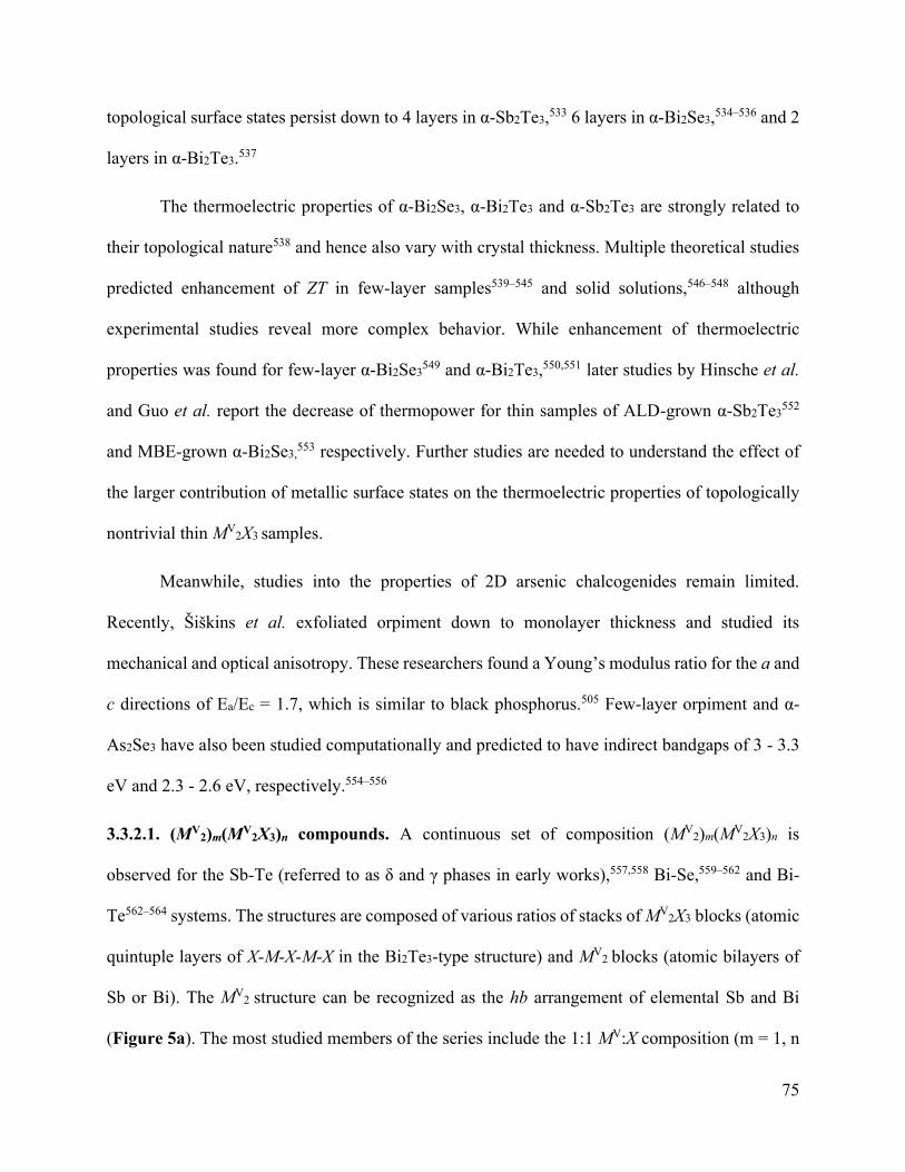
75
topological surface states persist down to 4 layers in α-Sb2Te3,533 6 layers in α-Bi2Se3,534–536 and 2
layers in α-Bi2Te3.537
The thermoelectric properties of α-Bi2Se3, α-Bi2Te3 and α-Sb2Te3 are strongly related to
their topological nature538 and hence also vary with crystal thickness. Multiple theoretical studies
predicted enhancement of ZT in few-layer samples539–545 and solid solutions,546–548 although
experimental studies reveal more complex behavior. While enhancement of thermoelectric
properties was found for few-layer α-Bi2Se3549 and α-Bi2Te3,550,551 later studies by Hinsche et al.
and Guo et al. report the decrease of thermopower for thin samples of ALD-grown α-Sb2Te3552
and MBE-grown α-Bi2Se3,553 respectively. Further studies are needed to understand the effect of
the larger contribution of metallic surface states on the thermoelectric properties of topologically
nontrivial thin MV2X3 samples.
Meanwhile, studies into the properties of 2D arsenic chalcogenides remain limited.
Recently, Siskins et al. exfoliated orpiment down to monolayer thickness and studied its
mechanical and optical anisotropy. These researchers found a Young’s modulus ratio for the a and
c directions of Ea/Ec = 1.7, which is similar to black phosphorus.505 Few-layer orpiment and α-
As2Se3 have also been studied computationally and predicted to have indirect bandgaps of 3 - 3.3
eV and 2.3 - 2.6 eV, respectively.554–556
3.3.2.1. (MV2)m(MV
2X3)n compounds. A continuous set of composition (MV2)m(MV
2X3)n is
observed for the Sb-Te (referred to as δ and γ phases in early works),557,558 Bi-Se,559–562 and Bi-
Te562–564 systems. The structures are composed of various ratios of stacks of MV2X3 blocks (atomic
quintuple layers of X-M-X-M-X in the Bi2Te3-type structure) and MV2 blocks (atomic bilayers of
Sb or Bi). The MV2 structure can be recognized as the hb arrangement of elemental Sb and Bi
(Figure 5a). The most studied members of the series include the 1:1 MV:X composition (m = 1, n
76
= 2) of SbTe563, BiSe563 and BiTe565,566 (Figure 11c), 2:1 MV:X composition (m = 2, n = 1) of
Sb2Te567 and Bi2Te,568,569 (Figure 11c), and 4:3 MV:X composition (m = 1, n = 1) of Sb4Te3,570
Bi4Se3571, Bi4Te3.572 Since there are two types of building blocks in these crystal structures, three
interlayer gaps are possible between the blocks: the gap between quintuple layers (MV2X3 to
MV2X3), the gap between the metal atomic bilayers (MV
2 to MV2), and the gap between the two
aforementioned blocks (MV2X3 to MV
2). The nature of the interlayer bonding between the blocks
differs for Sb and Bi compounds. In the case of antimony tellurides, all three gaps are vdW in
nature558,573,574 and the Sb2Te3-Sb2Te3, Sb2-Sb2, and Sb2Te3-Sb2 interlayer distances are 2.7 Å, 2.2-
2.3 Å, and 2.4-2.5 Å, respectively. For comparison, the Sb2Te3-Sb2Te3 interlayer distance is 2.8 Å
in the α-Sb2Te3 structure.558 In the case of bismuth selenides and tellurides, the distances between
Bi2X3 blocks remain large (2.6-2.7 Å) and hence the bonding is vdW. In contrast, the Bi2X3-Bi2
interlayer distances are shorter (2.2 Å) as compared to the Sb-Te system and the bonding is
considered to be weakly covalent.560,575 As a result, the crystal structure of BiTe features vdW gaps
between adjacent Bi2Te3 blocks (Figure 11c), whereas the crystal structure of Bi4Te3, which
consists of alternating Bi2 and Bi2Te3 blocks, does not feature any vdW gaps. While in most cases
a given (MV2)m(MV
2X3)n composition corresponds to a specific structure, the n, m pair does not
uniquely define the stacking order. For example, the structure of Sb4Te3 has been observed both
with576 and without577 the Sb2-Sb2 sequence, and MBE growth results in the mixture of both.570
The Bi2-Bi2 sequence is less common in comparison to the Sb2-Sb2 sequence in the antimony
tellurides, although reports exist of Bi2Te as well as further members of the series featuring Bi2-
Bi2 neighbors.568,569 In accordance with the trend for the hb-structured group V elements (section
2.3.1), the interlayer interaction (i.e., hb-hb interaction) for Bi2-Bi2 sequences is stronger than for
Sb2-Sb2.

77
Similar to the MV2X3 compounds, members of the (MV
2)m(MV2X3)n series show
topologically nontrivial properties and are thermoelectrics.568,574,578–582 Different surface
terminations and termination-dependent electronic properties have been identified for cleaved
Sb2Te573 and Bi4Se3580 crystals by ARPES studies where a complex interplay between structure
and surface electronic properties was discovered. BiTe was recently discovered to be a dual 3D
topological insulator (weak topological insulator and topological crystalline insulator phases
simultaneously) and also showed termination-dependent surface states.565,575 These findings
suggest ample opportunity for further study of the members of (MV2)m(MV
2X3)n series in the 2D
limit.
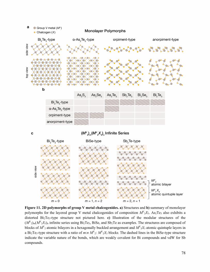
78
Figure 11. 2D polymorphs of group V metal chalcogenides. a) Structures and b) summary of monolayer
polymorphs for the layered group V metal chalcogenides of composition MV2X3. As2Te3 also exhibits a
distorted Bi2Te3-type structure not pictured here. c) Illustration of the modular structures of the
(MV2)m(MV
2X3)n infinite series using Bi2Te3, BiSe, and Sb2Te as examples. The structures are composed of
blocks of MV2 atomic bilayers in a hexagonally buckled arrangement and MV
2X3 atomic quintuple layers in
a Bi2Te3-type structure with a ratio of m:n MV2: M
V2X3 blocks. The dashed lines in the BiSe-type structure
indicate the variable nature of the bonds, which are weakly covalent for Bi compounds and vdW for Sb
compounds.

79

80
Table 5. Structures and electronic properties of group V metal chalcogenides of composition MV2X3.
name structure
type
space
group lattice parameters (Å) electronic properties refs
As2S3 bulk
orpiment orpiment P21/c
a = 11.48
b =9.58
c = 4.26
β = 90.7°
direct bandgap of 2.5-2.7 eV,
electron mobility of ~ 1 cm2 V-1 s-1 498,583–586
anorpiment anorpiment 𝑃1
a = 5.758
b = 8.717
c = 10.268
α = 78.15
β = 75.82
γ =89.86
indirect bandgap of ~ 2.4 eVa 501,587
monolayer - orpiment – a = 11.3a indirect bandgap of 3 - 3.3 eVa 505,554–556
As2Se3 bulk α-As2Se3 orpiment P21/c
a = 12.077
b =9.904
c = 4.284
β = 90.46°
direct bandgap of 1.75-1.85 eV 503,583,585,588
monolayer - orpiment – a = 12.1a indirect bandgaps of 2.3 - 2.6 eVa 554–556
As2Te3
bulk
α-As2Te3 α-As2Te3 C2/m
a = 14.337
b =4.015
c = 9.887
β = 95.06°
bandgap of 0.43-0.48 eV,
ZT of ~0.001 (RT)b 507,508,520
β-As2Te3 Bi2Te3 𝑅3𝑚 a = 4.047
c = 29.498
bandgap of 0.24-0.3 eVa,
Hall mobility of ~50 cm2 V-1 s-1,
ZT of ~0.2 (RT)b
508,516,589,590
β`-As2Te3 β`-As2Te3 P21/m
a = 6.996
b =16.241
c = 10.254
β = 103.43°
bandgap of 0.39 eVa 508,590
monolayer - Bi2Te3 – – indirect bandgap of 1.1 eVa 555
- orpiment – a = 13.1a indirect bandgap of 1.8 eVa 556
Sb2Te3
bulk α-Sb2Te3 Bi2Te3 𝑅3𝑚 a = 4.264
c = 30.46
topological insulator,
bulk bandgap of 0.24 eV, Hall
mobility on the order of 102 cm2 V-1 s-
1 (RT),
zT of ~0.3 (RT)b
494,591–593
monolayerc - Bi2Te3 – a = 4.3a indirect bandgap of 0.7 eV,
ZT up to 2 (RT)a 533,540,541,594,595
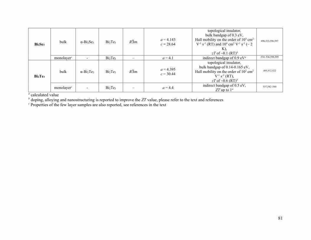
81
Bi2Se3 bulk α-Bi2Se3 Bi2Te3 𝑅3𝑚
a = 4.143
c = 28.64
topological insulator,
bulk bandgap of 0.3 eV,
Hall mobility on the order of 103 cm2
V-1 s-1 (RT) and 104 cm2 V-1 s-1 (~ 2
K),
zT of ~0.1 (RT)b
496,523,596,597
monolayerc - Bi2Te3 – a = 4.1 indirect bandgap of 0.9 eVa 534–536,598,599
Bi2Te3
bulk α-Bi2Te3 Bi2Te3 𝑅3𝑚 a = 4.395
c = 30.44
topological insulator,
bulk bandgap of 0.14-0.165 eV,
Hall mobility on the order of 102 cm2
V-1 s-1 (RT),
zT of ~0.6 (RT)b
495,512,522
monolayerc - Bi2Te3 – a = 4.4 indirect bandgap of 0.5 eV,
ZT up to 1a 537,542–544
a calculated value b doping, alloying and nanostructuring is reported to improve the ZT value, please refer to the text and references c Properties of the few layer samples are also reported, see references in the text

82
3.3.2. Polymorph control of 2D group V metal chalcogenides
3.3.2.1. Growth. Polymorph control via growth is mostly realized for the Sb-Te, Bi-Se, and Bi-
Te systems within the (MV2)m(MV
2X3)n series. In contrast, the growth of arsenic chalcogenides
primarily results in amorphous films600 and hence polymorph control via growth remains
challenging. A review by Ginley et al. summarizes efforts in growing α-Sb2Te3, α-Bi2Se3, and α-
Bi2Te3 compounds using MBE.601 Precise control over the beam flux allows access to
stoichiometries beyond MV2X3 to other phases belonging to the (MV
2)m(MV2X3)n series as has been
demonstrated for the MBE growth of Sb2Te and SbTe,578 Sb4Te3,570 Bi-Se602 and Bi-Te 570,582,603
compounds. While it is possible to achieve growth of compounds with small m and n, the pure
growth of other members of the series is highly challenging due to disorder. These polymorphs are
close to each other in composition and thus even small variations in the flux or other growth
conditions result in a formation of stacking faults and disorder.570,602,603 The growth of MV2X3
phases and control over (MV2)m(MV
2X3)n stoichiometry have also been realized with CVD,604,605
MOCVD,606–608 MOVPE,609 PLD,610–612 PVT,613 sputtering,614,615 and other methods.616
While polytypism is not common for the group V metal chalcogenides, Rotunno et al. grew
the 1T polytype of Sb2Te3 (space group 𝑃3𝑚1) in the form of nanowires using MOCVD.617 The
structure consists of Te-Sb-Te-Sb-Te quintuple layers stacked exactly on top of each other in
contrast to the translational offset observed in the typical 3R stacking arrangement. The 1T
polytype is believed to be stabilized by the nanowire geometry and surface energy of the facets.
3.3.2.1. Pressure and Temperature. The application of hydrostatic pressure, often in combination
with elevated temperatures, is a common strategy for altering the structures of bulk group V metal
chalcogenides. These studies may provide a starting point for future work into 2D polymorph
control. Several layered polymorphs of group V metal chalcogenides accessed at high pressures

83
are stable at ambient conditions upon releasing the pressure, and the existence of such polymorphs
indicates a possibility of achieving the structures in the 2D form.
α-As2Se3 is reported to transition to β phase (α-As2Te3) at pressures of 3-5 GPa and
temperatures of 300-650 °C, and subsequently changes to γ-As2Se3 at 7 GPa and 950 °C, both of
which are stable at room temperature and atmospheric pressure.618,619 The structural details of γ-
As2Se3 are unknown. At 1050 °C and 7 GPa, As2Se3 is reported to disproportionate to AsSe and
AsSe2, the latter of which has an MoS2-type structure (space group R3m).619 Similarly, orpiment
(As2S3) disproportionates above 6 GPa and 600 °C to AsS and AsS2.620 The structure of AsS (space
group Pca21) has As–As bonds of 2.4-2.6 Å and consists of washboard-like layers separated by
vdW gaps reminiscent of the sw/aw structure motif observed in the group V elements and group
IV monochalcogenides.621 AsS2 (space group P21) is composed of chains with S–S bonds (2.0 –
2.1 Å) that are separated by vdW gaps.622 Early studies report a transition of α-As2Te3 to β-As2Te3
at 6-8 GPa.623 However, later reports assigned the 6-8 GPa transition to metallisation of α-As2Te3
followed by a structural transition to non-layered γ-As2Te3 (isostructural to γ-Bi2Te3, space group
C2/c) above ~13-17 GPa.624,625
Bulk Sb2Te3, Bi2Se3, and Bi2Te3 display rich polymorphism at high pressure, which is
detailed in the reviews by Manjón et al.626 and Morozova et al.627 The α phase (Bi2Te3-type) is
reported to transition to a β-phase at 8-10 GPa, which is the only layered high-pressure polymorph
and features heptacoordinated M cations. It is worth noting that at ~4 GPa, α-Sb2Te3, α-Bi2Se3 and
α-Bi2Te3 undergo isostructural phase transitions associated with anomalies in mechanical,
electrical, and thermodynamic properties. This transition is often assigned to an electronic
topological transition (i.e., a second order isostructural phase transition associated with the change
of the Fermi energy surface topology),626 although recent reports suggest alternative mechanisms
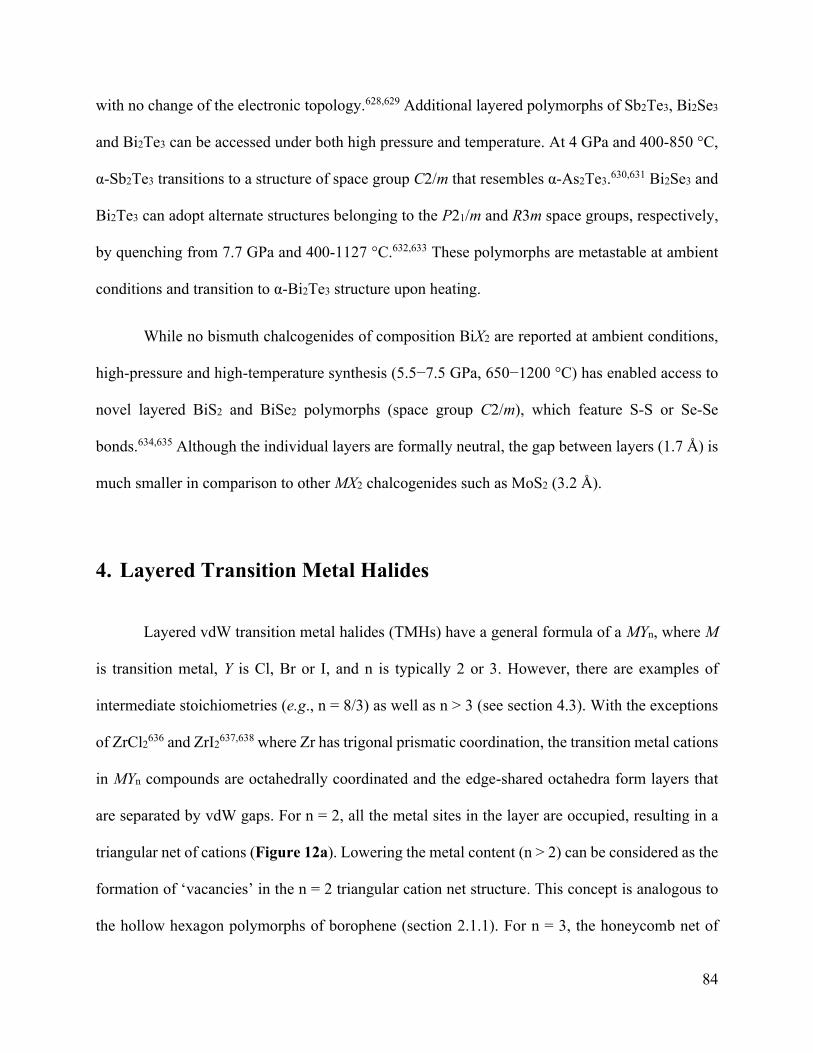
84
with no change of the electronic topology.628,629 Additional layered polymorphs of Sb2Te3, Bi2Se3
and Bi2Te3 can be accessed under both high pressure and temperature. At 4 GPa and 400-850 °C,
α-Sb2Te3 transitions to a structure of space group C2/m that resembles α-As2Te3.630,631 Bi2Se3 and
Bi2Te3 can adopt alternate structures belonging to the P21/m and R3m space groups, respectively,
by quenching from 7.7 GPa and 400-1127 °C.632,633 These polymorphs are metastable at ambient
conditions and transition to α-Bi2Te3 structure upon heating.
While no bismuth chalcogenides of composition BiX2 are reported at ambient conditions,
high-pressure and high-temperature synthesis (5.5−7.5 GPa, 650−1200 °C) has enabled access to
novel layered BiS2 and BiSe2 polymorphs (space group C2/m), which feature S-S or Se-Se
bonds.634,635 Although the individual layers are formally neutral, the gap between layers (1.7 Å) is
much smaller in comparison to other MX2 chalcogenides such as MoS2 (3.2 Å).
4. Layered Transition Metal Halides
Layered vdW transition metal halides (TMHs) have a general formula of a MYn, where M
is transition metal, Y is Cl, Br or I, and n is typically 2 or 3. However, there are examples of
intermediate stoichiometries (e.g., n = 8/3) as well as n > 3 (see section 4.3). With the exceptions
of ZrCl2636 and ZrI2
637,638 where Zr has trigonal prismatic coordination, the transition metal cations
in MYn compounds are octahedrally coordinated and the edge-shared octahedra form layers that
are separated by vdW gaps. For n = 2, all the metal sites in the layer are occupied, resulting in a
triangular net of cations (Figure 12a). Lowering the metal content (n > 2) can be considered as the
formation of ‘vacancies’ in the n = 2 triangular cation net structure. This concept is analogous to
the hollow hexagon polymorphs of borophene (section 2.1.1). For n = 3, the honeycomb net of
85
cations is formed (Figure 12b). The voids can be occupied by the same metal cations to form solid
solutions of MY2-MY3639 or by other guest cations. The former was experimentally observed in
single crystals of VI3640,641 and VBr3,642 although the partial occupancy was attributed to the
presence of stacking faults in the crystals.
In comparison to metal chalcogenides, metal halides feature more ionic bonding and hence
greater charge separation between the metal and halogen atoms. Such charge localization generally
results in lower charge carrier mobilities. In fact, most of the TMHs are Mott insulators. Moreover,
the angular momentum associated with partially filled d orbitals of the transition metal cations
gives rise to magnetic order. As a result, layered vdW TMHs present a rich spectrum of
possibilities related to 2D magnetism and spintronics. Theoretical studies predict low cleavage
energies for most layered vdW TMHs,643–646 suggesting the possibility of monolayer TMHs via
exfoliation from the bulk or bottom-up vdW epitaxy. The exploration of 2D TMHs is relatively
nascent and thus much work is still required to investigate the structures and properties of their 2D
forms. For more details regarding the magnetic properties of bulk TMHs please see the review by
McGuire.647
Due to the low vdW interlayer binding strength, stacking faults or polytypes are commonly
observed in layered MYn compounds, although they are often difficult to distinguish
experimentally. Stacking variations can occur during heating or cooling of MYn crystals through
structural transition temperatures or during growth, 648 as well upon mechanical deformation such
as during micromechanical exfoliation.649,650 Similarly, atomic force microscopy studies of layered
vdW TMHs have shown that the applied tip force can alter the structure of TMH crystals. For
example, Bengel et al. report drastic changes of the atomic force microscopy images of transition
metal trichlorides produced with large applied forces and explain their observation by tip-force-
86
induced surface corrugation.651 A recent single-spin magnetometry study also reports a strong
change of magnetization (most likely caused by a structural change) after physical puncture of the
CrI3 flake on the substrate.652 These results indicate that even if the structure of the bulk crystal is
well established, control over the symmetry and stacking becomes vital for 2D TMH samples that
are often produced by scotch-tape exfoliation and thus undergo mechanical deformation during
preparation.
It should also be noted that most layered vdW TMHs are not stable in ambient conditions,
adding further complexity to their characterization. Reaction of the TMH with ambient water starts
from the edge until the entire crystal is ‘dissolved’ in the absorbed water.653 As a result, most
experimental studies on exfoliated TMHs are performed in gloveboxes and vacuum chambers
and/or with encapsulation schemes (e.g., sandwiching the TMH flake between hBN flakes) to
protect the crystals from ambient exposure.
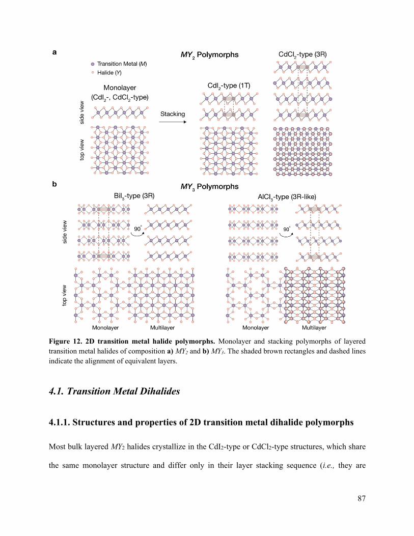
87
Figure 12. 2D transition metal halide polymorphs. Monolayer and stacking polymorphs of layered
transition metal halides of composition a) MY2 and b) MY3. The shaded brown rectangles and dashed lines
indicate the alignment of equivalent layers.
4.1. Transition Metal Dihalides
4.1.1. Structures and properties of 2D transition metal dihalide polymorphs
Most bulk layered MY2 halides crystallize in the CdI2-type or CdCl2-type structures, which share
the same monolayer structure and differ only in their layer stacking sequence (i.e., they are
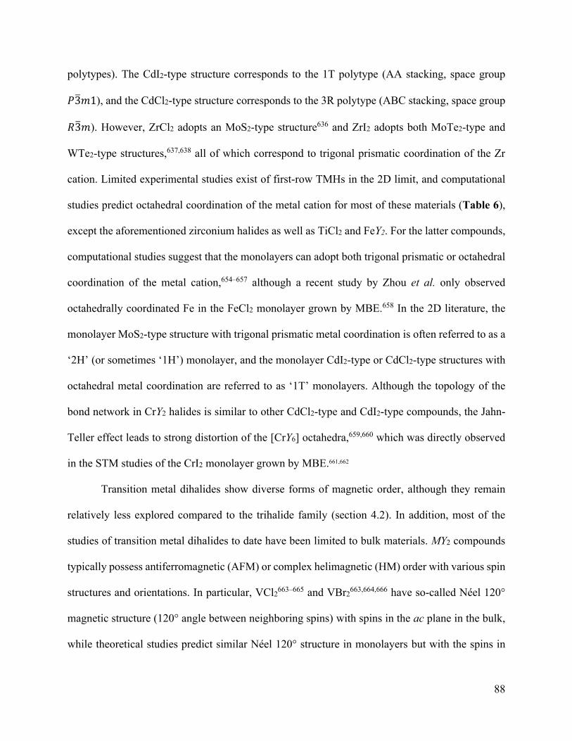
88
polytypes). The CdI2-type structure corresponds to the 1T polytype (AA stacking, space group
𝑃3𝑚1), and the CdCl2-type structure corresponds to the 3R polytype (ABC stacking, space group
𝑅3𝑚). However, ZrCl2 adopts an MoS2-type structure636 and ZrI2 adopts both MoTe2-type and
WTe2-type structures,637,638 all of which correspond to trigonal prismatic coordination of the Zr
cation. Limited experimental studies exist of first-row TMHs in the 2D limit, and computational
studies predict octahedral coordination of the metal cation for most of these materials (Table 6),
except the aforementioned zirconium halides as well as TiCl2 and FeY2. For the latter compounds,
computational studies suggest that the monolayers can adopt both trigonal prismatic or octahedral
coordination of the metal cation,654–657 although a recent study by Zhou et al. only observed
octahedrally coordinated Fe in the FeCl2 monolayer grown by MBE.658 In the 2D literature, the
monolayer MoS2-type structure with trigonal prismatic metal coordination is often referred to as a
‘2H’ (or sometimes ‘1H’) monolayer, and the monolayer CdI2-type or CdCl2-type structures with
octahedral metal coordination are referred to as ‘1T’ monolayers. Although the topology of the
bond network in CrY2 halides is similar to other CdCl2-type and CdI2-type compounds, the Jahn-
Teller effect leads to strong distortion of the [CrY6] octahedra,659,660 which was directly observed
in the STM studies of the CrI2 monolayer grown by MBE.661,662
Transition metal dihalides show diverse forms of magnetic order, although they remain
relatively less explored compared to the trihalide family (section 4.2). In addition, most of the
studies of transition metal dihalides to date have been limited to bulk materials. MY2 compounds
typically possess antiferromagnetic (AFM) or complex helimagnetic (HM) order with various spin
structures and orientations. In particular, VCl2663–665 and VBr2
663,664,666 have so-called Néel 120°
magnetic structure (120° angle between neighboring spins) with spins in the ac plane in the bulk,
while theoretical studies predict similar Néel 120° structure in monolayers but with the spins in
89
the ab plane.667 MnBr2668 and FeI2
669–671 have stripes of spins running through the crystal where
the stripes are arranged with AFM order. The iron, cobalt, and nickel chlorides and bromides all
exhibit ferromagnetically (FM) coupled intralayer spins with AFM interlayer interactions,
although the spin orientations differ among these compounds (Table 6).672,673 Finally, MnI2,668,674–
676 CoI2,677–679 NiI2677,680 and NiBr2
681–685 possess complex HM ground state order. These halides are
also reported to show multiferroic behaviour,676,679,685 which opens the possibility for electrical
control of magnetism. Moreover, iron halide monolayers have been predicted to show half-
metallicity (i.e., metallic behaviour for one spin orientation and insulating for another).645,686 A
summary of the structures, properties, and magnetic ordering of MY2 compounds in the bulk
(experimental data) and in the monolayer form (calculated values) is presented in Table 6.
Additionally, a review by McGuire contains further details on the magnetic properties of bulk MY2
compounds.647
90
Table 6. Structures, magnetic properties, and electronic properties of monolayer and bulk transition metal dihalides.
structure type
(space group) at
RT
lattice
parameters
(Å)
magnetic order and spin
orientation
temperature
of magnetic
order (K)
electronic
properties ref(s)
TiCl2 bulk CdI2 (𝑃3𝑚1) a = 3.561, c = 5.875 AFM 85 – 687–689
monolayer trigonal prismatic – AFM ∥ c – – 654
TiBr2 bulk CdI2 (𝑃3𝑚1) a =3.629, c = 6.492 – – – 688–690
monolayer octahedral – AFM ∥ c – – 654
TiI2 bulk CdI2 (𝑃3𝑚1) a = 4.11, c = 6.82 – – – 688,689,691
monolayer octahedral – AFM ∥ c – – 654
ZrCl2 bulk MoS2 (R3m) a = 3.382, c = 19.378 – – – 636,688,689
monolayer trigonal prismatic – – – – 654
ZrI2
bulk α-ZrI2 MoTe2 (𝑃21/𝑚) a = 6.821, b = 3.741,
c = 14.937, β = 95.66 – – – 637,689
bulk β-ZrI2 WTe2 (𝑃𝑚𝑛21) a = 3.744, b =6.831, c
= 14.886 – – – 638
monolayer trigonal prismatic – – – – 654
VCl2 bulk CdI2 (𝑃3𝑚1) a = 3.60, c = 5.83 AFM-120°, ∥ ac plane 36 – 663–665,692
monolayer octahedral a = 3.6 AFM-120°, ⊥ c – insulator 643,654,667,693–695
VBr2 bulk CdI2 (𝑃3𝑚1) a = 3.76, c = 6.18 AFM-120°, ∥ ac plane 30 – 663,664,666,691
monolayer octahedral a = 3.81 AFM-120°, ⊥ c – insulator 643,654,667,693–695
VI2 bulk CdI2 (𝑃3𝑚1) a = 4.057, c = 6.760 AFM 16.3, 15 – 663,664,696
monolayer octahedral a = 4.08 AFM-120°, ⊥ c – insulator 643,654,667,693–695
CrBr2 bulk 𝐶2/𝑚
a = 7.11, b = 3.65, c =
6.22, β = 93.88 – – – 659
monolayer octahedral a = 3.7 AFM – half-metal 643,695
CrI2 bulk 𝐶2/𝑚
a = 7.55, b = 3.93, c =
7.51, β = 115.52 – – – 660
monolayer octahedral a = 3.9 – 4.2 FM – insulator 661,662
MnCl2 bulk CdCl2 (𝑅3𝑚) a = 3.711, c = 17.59 AFM stripe ⊥ c or HM 2, 1.8 insulator 669,697,698
monolayer octahedral a = 3.64 multiple structures proposed – insulator 643,654,693–695,699
MnBr2 bulk CdI2 (𝑃3𝑚1)a a = 3.868, c = 6.272 AFM stripe ⊥ c 2.3, 2.16 insulator 668,669,700
monolayer octahedral a = 3.84 AFM-120° or stripe ⊥ c – insulator 643,654,693–695
MnI2 bulk CdI2 (𝑃3𝑚1) a = 4.146, c = 6.829 HM
3.95, 3.8,
3.45
insulator
multiferroic 668,669,674–676
monolayer octahedral a = 4.12 AFM-120° or stripe ⊥ c – insulator 643,654,693–695
FeCl2 bulk CdCl2 (𝑅3𝑚) a = 3.598, c = 17.536 AFM ∥ c 24 insulator 669,672,701

91
monolayer octahedral a = 3.4-3.5
FM ∥ c 100-160 half-metal 643,654–
658,686,693,694,702 trigonal prismatic a = 3.36
FeBr2
bulk CdI2 (𝑃3𝑚1) a = 3.776, c = 6.227 AFM ∥ c 14 insulator 669,672,703
monolayer octahedral a = 3.69
FM ∥ c 80-200 half-metal 643,654,656,693,694 trigonal prismatic a = 3.57
FeI2
bulk CdI2 (𝑃3𝑚1) a = 4.03, c = 6.75 AFM ∥ c, stripes 9 insulator 669–671
monolayer octahedral a = 3.98
FM ∥ c 40-120 half-metal 643,654,656,693,694 trigonal prismatic a = 3.87
CoCl2 bulk CdCl2 (𝑅3𝑚) a = 3.553, c = 17.359 AFM ⊥ c 25 insulator 672
monolayer octahedral a = 3.49 multiple structures proposed – half-metal 643,654,693–695
CoBr2
bulk CdI2 (𝑃3𝑚1) a = 3.728, c = 6.169 AFM ⊥ c 19 insulator 672
monolayer octahedral a = 3.63 multiple structures proposed – insulator 643,644,654,693–
695,704
CoI2 bulk CdI2 (𝑃3𝑚1) a = 3.985, c = 6.664 HM 11
insulator
multiferroic 677–679
monolayer octahedral a = 3.92 AFM – insulator 643,654,693–695
NiCl2
bulk CdCl2 (𝑅3𝑚) a = 3.483, c = 17.40 AFM ⊥ c 52 insulator 673,705,706
monolayer octahedral a = 3.45 FM ∥ c 60-200 insulator 643,654,693–
695,707–709
NiBr2
bulk CdCl2 (𝑅3𝑚) a = 3.704, c = 18.31 AFM ⊥ c, HM 52, 23 insulator
multiferroic 681–685,710
monolayer octahedral a = 3.64 FM ∥ c 130-170 insulator 643,654,693–
695,707–709
NiI2
bulk CdCl2 (𝑅3𝑚)b a = 3.922, c = 19.808 HM 75 insulator
multiferroic 677,680
monolayer octahedral a = 3.92 FM ∥ c 130-180 insulator 643,654,693–
695,707–709,711
Entries for bulk structures are based on experiment and monolayer entries are based on calculations
‘Octahedral’ indicates a CdI2-type or CdCl2-type monolayer structure with octahedral coordination of the metal cation
‘Trigonal prismatic’ indicates an MoS2-type monolayer structure with trigonal prismatic coordination of metal cation aMnBr2 transitions to CdCl2-type structure above 623 K bNiI2 transitions to monoclinic structure below 60 K
92
4.1.2. Polymorph control of 2D transition metal dihalides
Reports of 2D transition metal dihalide growth are limited to UHV-MBE CrI2661,662 and FeCl2.658
In both cases, the structure of the 2D layer resembles the bulk (i.e., octahedrally coordinated Cr
and Fe), although a number of theoretical studies predicted trigonal prismatic coordination for
monolayer FeCl2.655–657,702 Stacking order as well as its influence on the magnetic and electronic
properties of these 2D films remain to be explored. Similarly, limited studies have experimentally
demonstrated polymorph control for 2D transition metal dihalides. However, the reports of
structural manipulation in the bulk provide a basis for such control in the ultrathin limit. Several
MY2 compounds are reported to undergo temperature-induced transitions from one polymorph to
another. In particular, MnBr2 transitions from the CdI2-type to CdCl2-type structure above 623
K.712 Furthermore, NiI2 adopts a monoclinic structure below ~60 K, along with the emergence of
helical antiferromagnetic order, although the exact structural details of this low-temperature NiI2
phase are not yet reported.677 Liu et al. report a slight decrease of the Néel temperature with
decreasing thickness in PVD grown NiI2,713 although it remains to be seen whether the thickness
of other MY2 crystals affects the transition temperatures observed in the bulk. Multiple reports of
such thickness dependencies in the transition metal trihalides (section 4.2.2) and group III metal
chalcogenides (section 3.1.2.3) suggest its likelihood.
The application of hydrostatic pressure has been explored to induce structural and phase
transitions in bulk MY2 compounds. FeCl2 transitions from the 3R polytype (CdCl2-type structure)
to the 1T polytype (CdI2-type structure) at 0.6 GPa.701 Two more phases of FeCl2 have been
reported at higher pressures, although both are of the CdI2-type structure. Specifically, at pressures
above 32 GPa, the spins cant away from the c axis and the Fe d electrons delocalize, leading to an
insulator-to-metal transition and collapse of magnetisation at higher pressures.714 A similar

93
insulator-to-metal transition has been observed for FeI2.714 CoCl2 was shown to transition from the
3R polytype (CdCl2-type structure) to a 2H polytype (CdI2-type modification) at 0.5 GPa followed
by another transition to the 1T polytype (CdI2-type structure).715 Further pressurization results in
an insulator-to-metal transition at ~70 GPa. Interestingly, metallization of CoCl2 was found to
occur due to p-d charge-transfer bandgap closure with the 3d electrons still localized, meaning that
metallization and magnetism can coexist until the occurrence of 3d electron delocalization at 180
GPa. An insulator-to-metal transition was also found for NiI2 at 16 GPa and is associated with
charge-transfer gap closure.680 Since NiI2 is non-magnetic above 19 GPa, the existence of a new
antiferromagnetic-metallic phase has been proposed between 17 and 19 GPa.716
Alloying has also been used to tune the structures of MY2 compounds. Specifically, since
all nickel halides have the same CdCl2-type structure, full solid solutions exist between NiBr2 and
NiI2. This strategy has been demonstrated to decrease the Néel temperature upon Br substitution
in NiI2.717 Additionally, NiBr2 has been shown to change from the CdCl2-type structure to the
CdI2-type structure upon Co substitution (around 56-76% of cobalt). The temperature-composition
phase diagram of the magnetic transitions shows that increasing the Co content decreases the Néel
temperature of the first NiBr2 transition (from a non-commensurate to a commensurate
antiferromagnetic structure) to 21 K at 56% Co concentration.718
4.2. Transition Metal Trihalides
4.2.1. Structures and properties of 2D transition metal trihalide polymorphs
Most layered transition metal trihalides have BiI3-type or AlCl3-type structures.647 In both cases,
the monolayer structure is based on the honeycomb cation sublattice, which can be constructed
94
from the MY2 monolayer by ‘removing’ every third metal cation. Both MY3 polymorphs have
similar stacking sequences: strictly 3R for BiI3-type (ABC stacking, space group 𝑅3) and ‘3R-
like’ for AlCl3-type (ABC stacking, space group 𝐶2/𝑚). The latter has a different layer shift
direction compared to the BiI3-type structure (Figure 12b). Furthermore, the AlCl3-type structure
has two types of crystallographic halide sites that allow for distortion of the [MY6] octahedra and
hence several different M-Y and M-M distances. In most cases, the distortion is minimal such that
the BiI3-type and AlCl3-type structures can essentially be considered polytypes. However, if the
distortion is strong (e.g., α-MoCl3 in section 4.2.1.4), then BiI3-type and AlCl3-type structures
should be considered as polymorphs rather than polytypes.
Polymorphism and polytypism in vdW-layered MY3 compounds play a crucial role in
determining their properties. Similar to the previous discussions on group III and IV metal
chalcogenides (section 3.1.1 and 3.2.1, respectively), the absence of an inversion center results in
strong SHG. Moreover, differences in the layer stacking order yield different topology of magnetic
exchange interactions, which in some cases causes different magnetic orders in two polytypes of
the same material (e.g., CrI3 in section 4.2.1.2). Similar to the layer-dependent ferroelectric
properties of SnS and SnTe,430,436 thickness-dependent magnetism is observed in CrBr3 and CrI3.
Furthermore, multiple MY3 compounds are reported to transition from one polymorph to another
upon cooling. For many MY3 compounds, this transition is crucial in determining their properties,
especially in the few-layer limit. A summary of the structure type, properties, and transition
temperatures of MY3 compounds is provided in Table 7.
4.2.1.1. Vanadium triiodide. Various crystal structures for the room-temperature and low-
temperature forms of VI3 have been proposed.640,719–721 Recent Raman spectroscopy studies
indicate a high-temperature AlCl3-type structure (𝐶2/𝑚),721,722 which transitions to a BiI3-type
95
structure (𝑅3) upon cooling.719,721 In contrast, a recent X-ray diffraction study suggests that VI3
adopts a BiI3-type structure at room temperature and transitions to a monoclinic phase at 79 K and
to a triclinic phase at 32 K,723 although the exact structural details are unknown.723 Furthermore,
two FM transitions are reported at ~50 K (second-order) and ~36 K (first order) that merge at a
pressure of 0.6 GPa.641,724 At 2 K, VI3 has large out-of-plane magnetic anisotropy with four-fold
symmetry and weak in-plane magnetic anisotropy with six-fold symmetry, but the exact ground
state magnetic structure remains unknown.725 Recent computational studies of bulk and monolayer
samples suggested that VI3 is a 2D Ising ferromagnet (easy c-axis magnetization).726 Wide-field
nitrogen-vacancy microscopy measurements allowed the imaging of magnetic domains and
domain reversal (at fields < 1 T at 5 K) for few-layer VI3 flakes encapsulated using hexagonal
boron nitride.727 The authors observed magnetic signal down to bilayer samples but no
magnetization was observed for monolayers, possibly due to imperfect encapsulation and
degradation. Moreover, for few-layer VI3 (2-9 layers), the authors observed lower magnetization
in comparison to bulk VI3 that could be explained by AFM interlayer coupling, as supported by
computation modelling.727 In line with these findings, Wang and Long considered two possible
structures of the VI3 bilayer and concluded that either the FM or AFM ground state is favored
depending on the stacking order.728 These results imply that stacking sequence (i.e., polytypism)
in VI3 has a dramatic influence on its magnetic configuration. In contrast, Long et al. predicted
stacking-independent ferromagnetism in bilayer VI3.729 Therefore, more experimental studies are
needed to clarify the magnetic order in VI3 in the few-layer limit.
Experimental studies report that bulk VI3 is a semiconductor with a bandgap between 0.6
and 0.7 eV.640,720 Correspondingly, theoretical studies predicted that bulk VI3 is a Mott-insulator
with a gap of 0.9 to 1 eV.719,720,726,728 However, some studies predict half-metallicity with no
96
bandgap.640,730,731 While there are no experimental reports on electronic transport in 2D VI3, recent
theoretical studies predict that monolayer726–728,732 and bilayer727 VI3 are Mott insulators while the
trilayer is a half-metal.727 Long et al. predicted bilayer VI3 to also be a half-metal.729
4.2.1.2. Chromium trihalides. Chromium halides are the most studied of the transition metal
halides. A number of unique properties are observed in these materials including thickness-
dependent and stacking-dependent magnetism, giant tunneling magnetoresistance, and electrical
control over the magnetic state. From Cl to I, the increase in atomic number results in larger SOC
as well as larger Cr-Cr distances that result in weaker direct exchange and dominant super
exchange interactions. All bulk CrY3 halides possess a high-temperature AlCl3-type structure and
transition to a BiI3-type structure upon cooling, although this transition occurs above room
temperature for CrBr3. The transition temperatures are given in Table 7. Notably, contrary to the
bulk, micromechanically exfoliated CrCl3 and CrI3 do not show the transition into the
rhombohedral BiI3-type structure and instead show signs of the monoclinic AlCl3-type structure at
low temperatures. A discussion on the proposed mechanisms for this discrepancy between bulk
and exfoliated samples of CrCl3 and CrI3 is provided in section 4.2.2.
Chromium halides possess different degrees of ambient stability with the chloride being
the most stable and the iodide being the most reactive with moisture.733 Exfoliated CrI3 flakes
degrade in air within minutes, and the degradation is accelerated under optical illumination.653All
halides show insulating behavior and therefore their properties are often probed by fabricating
tunneling devices. These measurements typically use graphene contacts in addition to sandwiching
between two hexagonal boron nitride flakes, where the flake stacking is performed in inert
environments, in an effort to minimize ambient degradation.
97
Chromium halides possess a range of magnetic ordering behavior, especially in the 2D
thickness regime. Bulk CrCl3 establishes its magnetic order in two stages (at 17 and 14 K),734,735
and the ground state magnetic structure has interlayer AFM coupling with FM ordered in-plane
spins with weak magnetic anisotropy.734,736 In few-layer CrCl3 crystals, the interlayer exchange
has been observed to be an order of magnitude larger in comparison to bulk CrCl3 (Figure 13a).
Furthermore, exfoliated CrCl3 flakes do not exhibit the monoclinic to rhombohedral structural
transition that occurs at 240 K for bulk crystals (Figure 13b).650 Both bulk CrBr3737 and
CrI3648,738,739 establish FM order at low temperature (37 K and 60.5 K, respectively) with the spins
lying along the c axis. Recent magnetometry740, photoluminescence741 and tunneling
measurements742 on exfoliated flakes have shown that CrBr3 remains FM down to the monolayer
limit. However, exfoliated CrI3 crystals instead exhibit AFM order below 45 K as measured by
magnetooptical Kerr effect (MOKE),743 photoluminescence744 and Raman spectroscopy,745,746 and
single-spin microscopy.652 While the spins in exfoliated CrI3 are still of FM order within the layer,
the layers are instead AFM coupled. As a result, exfoliated CrI3 crystals with an even number of
layers show net AFM behavior, whereas flakes with an odd number of layers show net FM order
due to the uncompensated magnetisation of a single layer. This observation has triggered
significant attention for CrI3 despite of its high ambient instability.
As discovered in spectroscopic and computational studies, the origin of the distinct
magnetic behaviour of thin CrI3 flakes (AFM below 45 K) compared to bulk crystals (FM below
60.5 K) lies in polymorphism, and more specifically, the layer stacking arrangement. Similar to
CrCl3, Raman spectroscopy and SHG showed that thin flakes of CrI3 remain in the monoclinic
AlCl3-type structure and do not undergo the structural transition at 210 K to the rhombohedral
BiI3-type structure as observed for bulk crystals.747,748 This insight is consistent with theoretical

98
studies showing that the interlayer exchange interactions of the AlCl3-type structure favor AFM
order while those of the BiI3-type phase favor FM order.749–752 Stacking-dependent magnetic order
(FM versus AFM) has also been observed in bilayer CrBr3 grown using MBE (Figure 13c,d) as
discussed further in section 4.2.2.753
The fabrication of devices from exfoliated chromium trihalide crystals has enabled further
investigation into their unique 2D magnetic properties. CrCl3 has been exfoliated down to the
monolayer limit733,735 and fabricated into tunneling heterostructures for probing the tunneling
current through CrCl3 as a function of its thickness, applied magnetic field, and temperature.650,754–
756 These studies allowed the construction of the magnetic phase diagram of exfoliated CrCl3 and
proposed a theoretical model for the spin-flip and spin-flop transitions.754,755 Ghazaryan et al.
discovered magnon-assisted tunneling through CrBr3, which opens the possibility for spin filtering
and spin injection.742 At room temperature, exfoliated CrI3 shows n-type semiconducting
behaviour with charge carrier field-effect mobilities on the order of 0.001 cm2 V-1 s-1, whereas CrI3
is insulating at low temperatures where magnetic ordering emerges.757 Additional studies of few-
layer CrI3 flakes showed giant tunneling magnetoresistance due to the spin-filtering effect as a
result of AFM order,757–760 memristive behavior,761 spin tunnel field-effect transistors,762 in
addition to other phenomena.763 Furthermore, electrostatic control of magnetism in bilayer CrI3
has been achieved by switching from AFM to FM order at an electron doping level of ~3 × 10¹³
764–766 or with an electric field on the order of 1 V nm-1 in a dual-gated geometry.767–769
4.2.1.3. Ruthenium trichloride. The exact structures of RuCl3 are still under debate due to
stacking faults in the crystals and similarities between possible polytypes. Both a trigonal phase
(space group 𝑃3112)770–772 and a AlCl3-type monoclinic phase773 have been reported at room
temperature. Cao et al. reported that the monoclinic structure persists throughout the whole
99
temperature range in RuCl3 single crystals with minimal stacking faults.774 However, recent reports
suggest a broad hysteretic transition (from 60 to 170 K) from the monoclinic AlCl3-type high-
temperature phase into a rhombohedral BiI3-type structure, similar to CrY3 halides.775–777
Additionally, a recent study by Dai et al. revealed reconstruction of the surface monolayer of bulk
RuCl3 crystals using surface-sensitive LEED.778 The authors proposed that Cl vacancies on the
surface of the flakes likely induced surface monolayer buckling and concomitant braking of the
inversion symmetry. Hence, the surface of RuCl3 crystals may be different from the bulk structure,
which is a phenomenon also suggested for CrI3 as discussed in section 4.2.2.
RuCl3 crystals show stacking-dependent magnetic transitions. Crystals with a minimal
amount of stacking faults generally show only one sharp transition at 7 K,771,774 which corresponds
to the so-called in-plane zigzag order and AFM alignment of layers with ABC stacking. RuCl3
crystals that posses more stacking faults instead show a magnetic order transition at 14 K, or both
14 K and 7 K.771,774,779 RuCl3 powders show only the broad 14 K transition. Moreover, crystals that
show the transition at 7 K can be transformed into crystals with only the 14 K transition via
mechanical deformation.771,774
RuCl3 has attracted significant theoretical and experimental attention as it was identified
as a candidate for the realization of a Kitaev spin liquid state.780–782 Signatures of the Kitaev spin
liquid state in RuCl3 (fractional magnetic excitations, Majorana fermions) have been observed by
a number of techniques including neutron scattering,783,784 NMR,785 and half-quantized thermal
Hall effect.786,787 For more details on the topic of realization of Kitaev spin liquid states, please see
the recent review by Takagi et al.782 Magnetic fields can induce the transition from the ordered
zigzag phase into a disordered state possibly related to the Kitaev quantum spin liquid, although
the exact magnetic field–temperature phase diagram of RuCl3 is not fully established.786,788,789
100
Studies of exfoliated RuCl3 flakes have uncovered the effect of flake thickness on the
emergence of the spin liquid state. Raman spectroscopy measurements have shown the presence
of the magnetic scattering continuum down to monolayer thicknesses, indicating a persistent
proximate quantum spin liquid state in the 2D limit.790–792 Additionally, these measurements
indicated a lowering of the symmetry in exfoliated RuCl3 through in-plane distortions, which was
found to correlate with the observed enhancement of anisotropy in the Kitaev exchange
constants.791 RuCl3 is a Mott insulator with a bandgap of 0.25 eV,793 and conductivity
measurements on single flakes indicated that it becomes insulating at low temperatures.649
Therefore, in order to access the magnetic properties of thin flakes, indirect measurements have
been explored by making a heterostructure of RuCl3 with graphene.794–797 These measurements
demonstrated electron transfer from graphene to RuCl3, allowing the investigation of proximity
effects (e.g., strain) and doping on the magnetic interactions in RuCl3. Additionally, while a
number of electrical circuits have been proposed to probe the spin liquid state in RuCl3,798 this
experimental strategy may prove to be challenging due to the low conductivity of RuCl3 at low
temperatures.
4.2.1.4. Other MY3 halides. TiCl3 exhibits multiple polytypes at room temperature. Early work
by Natta et al. reports α, β and γ polymorphs, as well as a δ polymorph which was obtained by
prolonged grinding of α- or γ-TiCl3.799 The α (BiI3-type) and γ (space group 𝑃3112) structures are
both are layered and differ only by their stacking order (i.e., they are polytypes).799 Later work by
Troyanov et al. identified four different layered polytypes of TiCl3 at room temperature: I (BiI3-
type), II (space group 𝑃312), III (space group 𝑃31𝑐), and ε (space group 𝑃3𝑚1).800,801 These
polytypes were first reported to transition into the monoclinic AlCl3-type structure below 220 K,800

101
although a later study by the same group assigned triclinic low-temperature structures to TiCl3 and
TiBr3 and revealed the presence of Ti-Ti interactions.801,802
Early reports showed that layered TiCl3 polymorphs are paramagnetic at room
temperature.803,804 The magnetic susceptibility has a broad maximum at 260 K (suggesting AFM
order) that quickly drops below 217 K.804 No magnetic order is present at 4 K, which is possibly
explained by the formation of Ti-Ti bonds below the phase transition at 217 K.805 Cavallone et al.
performed electrical806 and optical807 measurements of α-TiCl3 and found semiconducting
behavior, and recent theoretical work showed that layered TiCl3 polymorphs are Mott insulators.808
No experimental studies of TiCl3 in the few-layer limit are reported, although Zhou et al. predicted
half metallicity in monolayer TiCl3809 and Geng et al. predicted that TiY3 are FM insulators.810
Multiple polytypes of FeCl3 are reported at room temperature: BiI3-type,811 as well as
structures of space group P312 and 𝑃3.812 FeCl3 has been shown to have a HM ground state with
the AFM coupled layers coupled below ~9 K,813,814 although a higher temperature of 15 K was
reported in an early neutron diffraction study.815 Subsequent studies report a field-induced spin-
flop magnetic phase transition at ~4 T.816 Based on Mössbauer-effect measurements, FeBr3 has
been shown to have a transition at ~16 K and an AFM ground state similar to FeCl3.817 While no
experimental results have been reported for iron halides in the few-layer limit, recent theoretical
studies predict that the monolayers of all iron halides are half-metals with FM order below 116 –
175 K.818,819 Another study by Liu et al. has explored possible magnetic structures of monolayer
FeCl3 and FeBr3 under strain, which led to the proposal that FeCl3 may host a spin liquid state.820
For MoCl3, two polymorphs are observed at room temperature: α- and β-MoCl3, both of
which belong to the 𝐶2/𝑚 space group821,822 Specifically, α-MoCl3 is of the AlCl3-type structure,
whereas β-MoCl3 is reported to have different stacking sequence with a higher density of stacking
102
faults and higher degree of disorder.821,823 At room temperature, α-MoCl3 is diamagnetic due to
dimerization of the Mo cations in the honeycomb lattice. Above 585 K, MoCl3 is reported to
transition to another AlCl3-type structure821,823 where the Mo-Mo dimers are broken such that the
Mo cations form a nearly regular honeycomb lattice, resulting in the sharp increase of the magnetic
susceptibility. Interestingly, McGuire et al. suggested the presence of strong AFM exchange within
this high-temperature MoCl3 phase, and calculated an order of magnitude higher magnetic
exchange interaction in comparison to CrCl3 and CrBr3.823 This observation suggests that if a
dimerization structural transition in α-MoCl3 is avoided and the high-temperature phase can be
retained, much higher magnetic transition temperatures can be expected in α-MoCl3 compared to
Cr halides.
All Rh and Ir halides crystallize in the AlCl3-type structure, and they are non-
magnetic.773,824–826 2D RhI3 was recently investigated through optoelectronic measurements and
found to exhibit a responsivity of 11.5 A W−1 and specific detectivity up to 2×10¹⁰ Jones at 980
nm.827 A computational study showed that semiconducting non-magnetic RhY3 monolayers can
display indirect-to-direct bandgap transitions upon application of in-plane strain and can develop
net magnetic moment upon electron doping.828
Multiple metal halides do not have vdW-layered bulk structures, but monolayers of these
compounds have been constructed and explored computationally. These materials could
potentially be accessed via bottom-up growth methods. Recent theoretical studies derived the
monolayer structures of RuBr3 and RuI3 from the RuCl3 structure and agreed on the possibility of
realizing these structures experimentally, but predicted different magnetic order and transition
temperatures.829,830 MnY3 monolayers were predicted to be intrinsic Dirac half-metals with high
charge carrier mobilities in addition to exhibiting FM order with high Curie temperatures.831

103
Motivated by the search for candidates that show the quantum anomalous Hall (QAH) effect at
room temperature, Ni, Pt, and Pd halides have recently been studied computationally. All NiY3
monolayers were identified to be intrinsic Dirac half-metals with high mobility and high-
temperature ferromagnetism, which are requirements for the room-temperature QAH effect.832–834
Similarly, PdCl3 has been predicted to be a Dirac half-metal with a high Curie temperature in the
monolayer form,835 and predicted to transition to a half-metal in the bilayer form and a
ferromagnetic metal with increasing number of layers.836 Monolayers of palladium and platinum
bromides and iodides have also been identified as ferromagnetic semiconductors and candidates
for the high-temperature QAH effect.837 In search of other topologically non-trivial materials,
PtCl3 was recently predicted to be a 2D Weyl half-semimetal.838
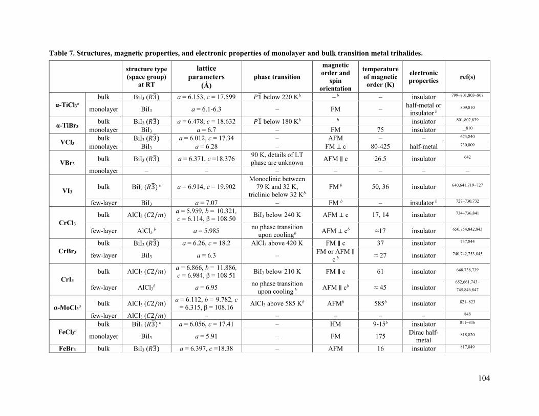
104
Table 7. Structures, magnetic properties, and electronic properties of monolayer and bulk transition metal trihalides.
structure type
(space group)
at RT
lattice
parameters
(Å)
phase transition
magnetic
order and
spin
orientation
temperature
of magnetic
order (K)
electronic
properties ref(s)
α-TiCl3a
bulk BiI3 (𝑅3) a = 6.153, c = 17.599 𝑃1 below 220 Kb – b – insulator 799–801,803–808
monolayer BiI3 a = 6.1-6.3 – FM – half-metal or
insulator b 809,810
α-TiBr3 bulk BiI3 (𝑅3) a = 6.478, c = 18.632 𝑃1 below 180 Kb – b – insulator 801,802,839
monolayer BiI3 a = 6.7 – FM 75 insulator –810
VCl3 bulk BiI3 (𝑅3) a = 6.012, c = 17.34 – AFM – – 673,840
monolayer BiI3 a = 6.28 – FM ⊥ c 80-425 half-metal 730,809
VBr3 bulk BiI3 (𝑅3) a = 6.371, c =18.376
90 K, details of LT
phase are unknown AFM ∥ c 26.5 insulator 642
monolayer – – – – – – –
VI3 bulk BiI3 (𝑅3) b a = 6.914, c = 19.902
Monoclinic between
79 K and 32 K,
triclinic below 32 Kb
FM b 50, 36 insulator 640,641,719–727
few-layer BiI3 a = 7.07 – FM b – insulator b 727–730,732
CrCl3
bulk AlCl3 (𝐶2/𝑚) a = 5.959, b = 10.321,
c = 6.114, β = 108.50 BiI3 below 240 K AFM ⊥ c 17, 14 insulator 734–736,841
few-layer AlCl3 b a = 5.985
no phase transition
upon coolingb AFM ⊥ cb ≈17 insulator 650,754,842,843
CrBr3
bulk BiI3 (𝑅3) a = 6.26, c = 18.2 AlCl3 above 420 K FM ∥ c 37 insulator 737,844
few-layer BiI3 a = 6.3 – FM or AFM ∥
c b ≈ 27 insulator 740,742,753,845
CrI3
bulk AlCl3 (𝐶2/𝑚) a = 6.866, b = 11.886,
c = 6.984, β = 108.51 BiI3 below 210 K FM ∥ c 61 insulator 648,738,739
few-layer AlCl3b a = 6.95
no phase transition
upon cooling b AFM ∥ cb ≈ 45 insulator
652,661,743–
745,846,847
α-MoCl3a
bulk AlCl3 (𝐶2/𝑚) a = 6.112, b = 9.782, c
= 6.315, β = 108.16 AlCl3 above 585 Kb AFMb 585b insulator 821–823
few-layer AlCl3 (𝐶2/𝑚) – – – – – 848
FeCl3a
bulk BiI3 (𝑅3) b a = 6.056, c = 17.41 – HM 9-15b insulator 811–816
monolayer BiI3 a = 5.91 – FM 175 Dirac half-
metal 818,820
FeBr3 bulk BiI3 (𝑅3) a = 6.397, c =18.38 – AFM 16 insulator 817,849
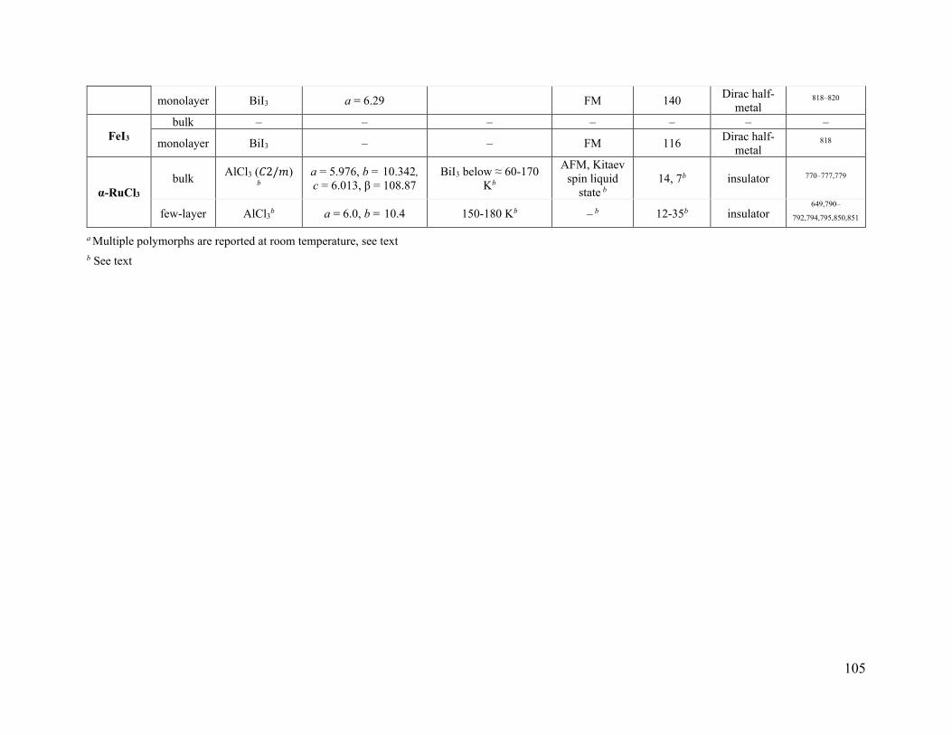
105
monolayer BiI3 a = 6.29 FM 140 Dirac half-
metal 818–820
FeI3
bulk – – – – – – –
monolayer BiI3 – – FM 116 Dirac half-
metal 818
α-RuCl3
bulk AlCl3 (𝐶2/𝑚)
b
a = 5.976, b = 10.342,
c = 6.013, β = 108.87
BiI3 below ≈ 60-170
Kb
AFM, Kitaev
spin liquid
state b
14, 7b insulator 770–777,779
few-layer AlCl3b a = 6.0, b = 10.4 150-180 Kb – b 12-35b insulator
649,790–
792,794,795,850,851
a Multiple polymorphs are reported at room temperature, see text
b See text

106
4.2.2. Polymorph control of 2D transition metal trihalides
Since the study of 2D transition metal halides is just beginning, the extent of experimental
polymorph control in 2D MY3 compounds is relatively limited. However, the significant influence
of structures and polytypes on magnetic properties suggests that polymorph control will be a
crucial engineering parameter for this class of materials. For both exfoliated CrCl3 and CrI3, the
structural transition from the high-temperature AlCl3-type structure to the Bi3-type structure that
is observed in the bulk is supressed. The mechanism behind the absence of this structural transition
in exfoliated samples is still under investigation. However, two of the leading proposed
explanations are: (1) preservation of the AlCl3-type structure through mechanical deformation and
stacking fault generation; (2) the AlCl3-type surface reconstruction that dominates the behavior of
2D samples.
Similar to what was discovered in RuCl3771,774,779 and RhI3,827 it has been suggested that
the mechanical stress generated by the exfoliation process can induce defects such as stacking
faults and grain boundaries that pin the high-temperature phase. This argument suggests that thick
exfoliated flakes should also show no structural transition, which was in fact observed for CrCl3.650
However, a study by Niu et al.852 used cryogenic magnetic force microscopy to probe the
magnetisation in CrI3 flakes thicker than 25 nm and found the coexistence of both 2D-like AFM
order below 45 K and bulk-like FM order below 60.5 K. The former AFM order was assigned to
approximately 20 layers (i.e., 13 nm thick), whereas the bulk of the crystal was asserted to be FM.
Together with the earlier studies, this work suggests that below 45 K, the surface of the thick flakes
has monoclinic symmetry (AlCl3-type structure), whereas the bulk is rhombohedral (BiI3-type). A
study by Li et al. suggested that this structural transition is triggered by magnetic order – namely,
at the onset of magnetic order, the surface layers change to the monoclinic stacking sequence while
107
the bulk of the crystal remains rhombohedral.853 Overall, further work is necessary to fully
understand the mechanism behind the preservation of the AlCl3-type structure in ultrathin
chromium halides and its influence on magnetic properties.
A recent study concerning the MBE growth of bilayer CrBr3 provides a rare example of
polytype and property control in vdW TMHs using synthesis methods.753 As depicted in Figure
13c,d, the authors observed AFM interlayer ordering for bilayer samples where the CrBr3 layers
were stacked in the same orientation (rhombohedral stacking, in analogy to AlCl3-type and BiI3-
type structures) and FM interlayer ordering when the layers were stacked with a relative 180º
rotation (hexagonal stacking). The hexagonal stacking is not reported for bulk CrBr3 crystals and
is thus a unique polytype for thin stacked samples. In this manner, the authors achieved explicit
control over interlayer magnetic ordering in 2D CrBr3 via assembly of distinct polytypes using
bottom-up methods. This study demonstrates the promise of vapor-phase growth efforts for
polymorph control in TMHs, although such synthesis of MY3 compounds remains challenging and
is limited to MoCl3,848 CrBr3753 and CrI3.661
The application of pressure and strain has also been employed to induce polymorph
conversions in MY3 compounds. Hydrostatic pressures of ~2-3 GPa were shown to irreversibly
change the AlCl3-type stacking order to BiI3-type in bilayer and few-layer CrI3 crystals, inducing
an AFM to FM phase transition (Figure 13e).854,855 Theoretical studies of strained few-layer CrI3
indicate the possibility of achieving other magnetic ground states including zigzag, Néel, and stripy
phases as well as states with in-plane spins.856–858 Indeed, strain tuning of the spin-flip transition
in bilayer CrI3 was recently demonstrated.859 In the case of bulk RuCl3, the application of
hydrostatic pressure resulted in a phase transition into the triclinic structure followed by Ru-Ru
dimerization from the overlap of the Ru 4d orbitals and complete suppression of the
108
magnetization,860,861 similar to the Mo and Zr trihalides (section 4.2.1.4). Raman spectroscopy
studies of exfoliated RuCl3 flakes revealed in-plane distortions of the RuCl3 lattice in the 2D
limit,790–792 and a recent theoretical study indicated that monolayer RuCl3 becomes strained when
in proximity to graphene.797
Irradiation of 2D transition metal trihalides may also provide another means for polymorph
control. Rodriguez-Vega et al. predicted that low-frequency IR light pulses can coherently drive
Raman phonon modes in bilayer CrI3, which can cause relative displacements between the layers
and hence affect the exchange interactions and magnetic order.862 Similarly, a recent theoretical
study predicted that optical pumping of RuCl3 monolayers could change the spin liquid phase to a
ferromagnetic phase due to doping-induced lattice strain and itinerant ferromagnetism.850
The use of doping and lithiation of TMHs has been explored both experimentally and
computationally to tune their structure and properties. Tartaglia et al. constructed a triangular
phase diagram of CrY3 compounds, which allowed tuning of the magnitude of the spin-orbit
interactions in the solid solutions.863 More studies should be performed to reveal the structural
details and properties of these compounds in the 2D limit. Recently, Cr doping in bulk RuCl3 was
shown to destabilize the zigzag RuCl3 order in favor of the spin glass state at 10% Cr doping.864
Lithiation of bulk RuCl3 was explored with both LiBH4865 and LiI,866 resulting in a decrease of the
temperature of the AFM order. It should be noted that the former account of lithiation with LiBH4
also included an exfoliation and restacking procedure following lithiation. Lithiation of mono-,
bi-, and trilayer CrI3 has also been predicted to fill the empty sites in the cation honeycomb lattice
and induce half-metallicity,867 while lithiation of monolayer CrBr3 has been predicted to induce
asymmetric Jahn-Teller distortions of the [CrBr6] octahedra for multiferroicity.868 A recent
theoretical study explored doping of V into monolayer VI3 (essentially a monolayer VI2-VI3 solid
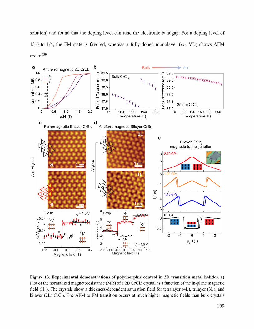
109
solution) and found that the doping level can tune the electronic bandgap. For a doping level of
1/16 to 1/4, the FM state is favored, whereas a fully-doped monolayer (i.e. VI2) shows AFM
order.639
Figure 13. Experimental demonstrations of polymorphic control in 2D transition metal halides. a)
Plot of the normalized magnetoresistance (MR) of a 2D CrCl3 crystal as a function of the in-plane magnetic
field (H||). The crystals show a thickness-dependent saturation field for tetralayer (4L), trilayer (3L), and
bilayer (2L) CrCl3. The AFM to FM transition occurs at much higher magnetic fields than bulk crystals
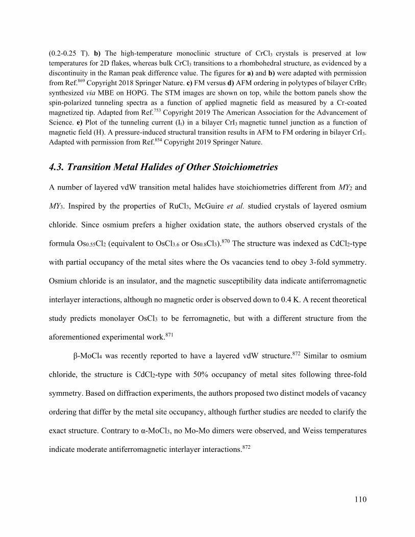
110
(0.2-0.25 T). b) The high-temperature monoclinic structure of CrCl3 crystals is preserved at low
temperatures for 2D flakes, whereas bulk CrCl3 transitions to a rhombohedral structure, as evidenced by a
discontinuity in the Raman peak difference value. The figures for a) and b) were adapted with permission
from Ref.869 Copyright 2018 Springer Nature. c) FM versus d) AFM ordering in polytypes of bilayer CrBr3
synthesized via MBE on HOPG. The STM images are shown on top, while the bottom panels show the
spin-polarized tunneling spectra as a function of applied magnetic field as measured by a Cr-coated
magnetized tip. Adapted from Ref.753 Copyright 2019 The American Association for the Advancement of
Science. e) Plot of the tunneling current (It) in a bilayer CrI3 magnetic tunnel junction as a function of
magnetic field (H). A pressure-induced structural transition results in AFM to FM ordering in bilayer CrI3.
Adapted with permission from Ref.854 Copyright 2019 Springer Nature.
4.3. Transition Metal Halides of Other Stoichiometries
A number of layered vdW transition metal halides have stoichiometries different from MY2 and
MY3. Inspired by the properties of RuCl3, McGuire et al. studied crystals of layered osmium
chloride. Since osmium prefers a higher oxidation state, the authors observed crystals of the
formula Os0.55Cl2 (equivalent to OsCl3.6 or Os0.8Cl3).870 The structure was indexed as CdCl2-type
with partial occupancy of the metal sites where the Os vacancies tend to obey 3-fold symmetry.
Osmium chloride is an insulator, and the magnetic susceptibility data indicate antiferromagnetic
interlayer interactions, although no magnetic order is observed down to 0.4 K. A recent theoretical
study predicts monolayer OsCl3 to be ferromagnetic, but with a different structure from the
aforementioned experimental work.871
β-MoCl4 was recently reported to have a layered vdW structure.872 Similar to osmium
chloride, the structure is CdCl2-type with 50% occupancy of metal sites following three-fold
symmetry. Based on diffraction experiments, the authors proposed two distinct models of vacancy
ordering that differ by the metal site occupancy, although further studies are needed to clarify the
exact structure. Contrary to α-MoCl3, no Mo-Mo dimers were observed, and Weiss temperatures
indicate moderate antiferromagnetic interlayer interactions.872

111
Niobium halides are known to crystallize in the Nb3Y8 stoichiometry. Their layered
structure consists of [Nb3Y13] clusters that are arranged in the triangular lattice. Kennedy et al.
reported five possible polytypes of clustered M3Y8 compounds,873 although only two are observed
for Nb halides: α-type (2T, space group 𝑃3𝑚1) is reported for Nb3Cl8, and β-type (6R, space group
𝑅3𝑚) is reported for Nb3Br8 and Nb3I8, as well as intercalated Nb3Cl8 (i.e., β-ANb3Cl8 where A is
alkali metal).873–877 α-Nb3Cl8 has been observed to transition from the room temperature trigonal
phase to a monoclinic C2/m structure at 90 K.878,879 This structural transition causes a paramagnetic
to nonmagnetic transition, and potential mechanisms include charge disproportionation879 and
second-order Jahn Teller distortion.878 A recent study on exfoliated α-Nb3Cl8 flakes revealed
insulating behavior and thickness-depended conductivity.880 β-Nb3Br8 was found to possess the
same paramagnetic to nonmagnetic transition as α-Nb3Cl8 at 387 K.876 Moreover, Pasco et al.
showed that the temperature of the phase transition can be tuned by varying the Cl/Br ratio in
Nb3Cl8-xBrx.876 Recent studies of exfoliated monolayer β-Nb3I8881 have reported semiconducting
behavior with a bandgap of ~1 eV,882 and a theoretical study predicted FM order in Nb3Y8
monolayers with Curie temperatures of 30-90 K.883 Another theoretical report predicted thickness-
dependent magnetic properties of 2D Nb3I8 as well as a Curie temperature near room temperature
for the monolayer.884 Contrary to niobium, bulk vanadium halides do not adopt the M3Y8
stoichiometry. However, it may be possible to obtain 2D forms of composition V3Y8. In particular,
a recent computational study by Xiao et al. predicted that monolayer V3Cl8, V3Br8, and V3I8 are
stable, with monolayer V3Cl8 being an intrinsic AFM semiconductor, and monolayer V3Br8 and
V3I8 being FM half-metals.885
5. Conclusions and Outlook
112
The exploration and manipulation of structural diversity in emerging post-dichalcogenide 2D
materials has only recently been undertaken and provides ample opportunity for 2D materials
engineering. This polymorphism encompasses several categories of structural variation: entirely
different monolayer structures (e.g., the group V elemental materials), stacking polytypes (e.g., the
group III metal chalcogenides and TMHs), and substrate-induced monolayer reconstructions (e.g.,
the group IV elemental materials). Since material structure dictates properties, this structural
diversity gives rise to a diversity in properties. In turn, the development of precise polymorphic
control methods enables explicit control and realization of desired material properties. For the
discussed 2D materials, the most powerful methods of polymorph control were achieved using
vapor-phase synthesis methods through the manipulation of growth conditions (e.g., temperature,
pressure, and precursor concentrations) and the synthesis substrate. As a result, progress in
polymorph control of post-dichalcogenide 2D materials relies on developments in their synthesis
via vapor-phase methods. Therefore, further work in developing improved vapor-phase synthesis
of post-dichalcogenide 2D materials, especially the TMHs, is necessary. Furthermore, non-
equilibrium synthesis methods such as pulsed laser deposition provide opportunities for targeting
metastable 2D material polymorphs.886
Moreover, while the phase diagrams and structures of bulk materials have been studied
systematically and thoroughly, this understanding is often not directly translatable to the 2D
regime. As surface effects become important – if not dominant – in the atomically thin limit, the
balance of forces that dictate the stability of different structures can change. For example, several
of the discussed 2D materials go through thickness-driven structural transformations as they enter
the 2D thickness regime. These materials include GaTe,379 SnTe,398,479 bismuthene,290 and some
vdW metal halides.652,743,744,869 Furthermore, several materials exhibit 2D polymorphs that are

113
stable at standard temperature/pressure conditions even though they are only observed in the bulk
at high temperatures/pressures, if at all. Specific examples in this category including several
elemental 2D materials (e.g., borophene,30,31 antimonene,215,216 bismuthene218) as well as
In2Se3.344,345 Therefore, opportunities exist for the re-evaluation of phase diagrams in the 2D
regime, which may accelerate the discovery of entirely new 2D polymorphs.
5.1. Discovery of 2D Polymorphs
The discovery of new 2D polymorphs can be guided using computational prediction.
Computational structure prediction underlies the fundamental mission of the Materials Genome
Initiative887 and has been specifically recognized as a pathway for the identification of metastable
polymorphs in the 2019 ‘Materials by Design’ roadmap.888 As machine learning, high-throughput
screening, and non-empirical search algorithms are becoming increasingly accessible,
computation methods are well positioned to uncover novel 2D structures that are beyond
experimental intuition.889 For example, several recent studies have focused on high-volume
prediction of 2D structures (Figure 14a).890,891 Moreover, several 2D polymorphs have been
experimentally synthesized with the help of computational efforts. These materials include
borophene,41,42,44 blue phosphorene,199 and 2D selenium and tellurium.892,893 In addition to the
elemental materials covered in this text, their alloys (e.g., IV-V) could provide another emergent
class of polymorphic 2D materials, where computational investigations allow for efficient
exploration of an experimentally daunting phase space.894–896 However, as evidenced by purely
synthetic 2D materials such as borophene, it is imperative to widen the search for 2D polymorphs
to non-vdW-layered parent materials. This concept is underlined by a computational study into
‘spontaneous graphitization’ by Sorokin et al., wherein the authors found that the structural

114
preference of bulk materials with 3D bonding may spontaneously shift to a layered structure below
a specific thickness (Figure 14b).897 Alternatively, a computational study by Liu et al. found the
substrate to play a significant role in facilitating interdimensional structural transformations.893
Hence, substrate and thickness effects alter the energetic playing field in the 2D regime and justify
a reconsideration of potential 2D material candidates.
5.2. Stabilization of 2D Polymorphs
Along with polymorph discovery, tactics for stabilizing metastable 2D polymorphs require further
research. A powerful and promising tool is substrate engineering. As discussed above, the use of
substrate symmetry or the strength of film-substrate interactions are essential methods in selecting
the desired 2D polymorph of a material. To template specific structures, the nature of the
interaction can range from pure vdW interfaces (e.g., ground-state hb-antimonene on hexagonal
PdTe2276 versus metastable aw-antimonene on orthorhombic Td-WTe2
281) to covalent interfaces
(e.g., planar bismuthene on SiC242, as shown in Figure 14c). Due to their lack of dangling bonds,
many 2D materials can grow via vdW epitaxy, enabling their deposition on a variety of substrates.
However, substrate engineering for 2D polymorph control is limited and requires further work,
especially as vapor-phase synthesis methods are being developed for emerging 2D materials. In
contrast, the principle of pseudomorphism, wherein metastable phases are stabilized via epitaxy,
has long been explored using MBE for 3D materials.898 Furthermore, more innovative forms of
epitaxy and templating have shown promise for 2D polymorphs. Specifically, confined epitaxy,
wherein the 2D layer is embedded within another structure, has resulted in novel 2D polymorphs.
Notably, 2D GaN was grown by Al Balushi et al. in between a bulk SiC substrate and a bilayer
graphene overlayer.899 Similarly, Wang et al. reported the growth of a CdI2-type monolayer of

115
metastable GeTe2 in a matrix of GeSb2Te4+x.487 In a more unconventional scheme, Gonzalez et al.
achieved the tailorable growth of 2D metal halides of formula MY2 inside metal-organic framework
templates (Figure 14c).900
Alternatively, the use of additives, dopants, or alloying presents another strategy to
stabilize metastable 2D polymorphs. For the 2D TMDs, lithium intercalation has been
demonstrated to stabilize both undistorted and distorted CdI2-type (1T) structures of monolayer
MoS2, while alloying with analogous elements (i.e., introduction of other transition metals or
chalcogens) has been shown to more subtly tune their structure.16 Additionally, the use of an alkali
element additive (potassium) during CVD of monolayer MoS2 has been reported to stabilize the
distorted CdI2-type (1T′) phase,901 and could prove useful for polymorph selection in other 2D
metal chalcogenides. However, with the exception these specific examples in 2D TMDs, the use
of additives, dopants, or alloying is under-investigated in the 2D materials research field.
In contrast, these strategies have worked well for bulk materials, highlighted here by
several recent reports. For perovskites, the incorporation of different organic ligands has been
shown to select between different metastable structures of CsPbI3.902 Rare-earth metal dopants
have been used to stabilize metastable structures of bulk materials such as Ag2WO4903 and
LaVO4,904 while mercury impurities have been employed to stabilize black As single-crystals.264
Furthermore, Zakutev and Lany et al. have recently investigated the implications of alloying
materials with different ground-state structures for the purpose of stabilizing metastable phases.905
For example, they realized wurtzite-type MnSe0.5Te0.5 by alloying rock-salt-type MnSe and
nickeline MnTe (Figure 14d).906 Lastly, surface functionalization of 2D materials such as the
group V elements has been predicted to enable structural control.175–177,295 This principle was
116
recently exemplified in a study by Fu et al., who obtained metastable cubic formamidinium lead
iodide at room temperature using surface functionalization with organic ligands.907
The search for suitable synthesis substrates, templates, or additives lends itself well to
combinatorial methods, which could accelerate efforts aimed at polymorph stabilization and
epitaxy. For example, Tomada et al. recently used combinatorial methods to explore different
molecular seeds for the growth of distinct chiralities of single-walled carbon nanotubes,908 while
Wittkamper et al. used a polycrystalline CoNb2O6 substrate to search for grain orientations that
stabilize the metastable scrutinyite-type SnO2 polymorph over the ground-state rutile-type SnO2
structure (Figure 14e).909 Furthermore, the use of compositional or substrate temperature gradients
can be used to combinatorially investigate narrow dopant concentrations or synthesis temperature
windows where particular metastable structures are obtained. The insight from combinatorial
synthesis can then feed directly into computational materials design and discovery, which is often
hindered by a lack of reliable and high-volume experimental data.
5.3. Polymorph Engineering and Functionality
Higher-order materials engineering and functionalities can be enabled by the variety of accessible
2D polymorphs and the methods used to stabilize them. Specifically, directed structural designs
can be achieved by integrating different polymorphs of a single material, as can be pursed through
either patterned conversion or self-assembly and growth. For instance, the patterned conversion
(using methods such as thermal annealing489 or irradiation with photons368 or electrons491) of a
high-resistance polymorph into a low-resistance polymorph has the potential to realize functional
homojunctions for contact engineering.910 The phase transformations themselves can also be
functional, as demonstrated by Choi et al. with switchable polymorph conversions in exfoliated
117
In2Se3 for phase-change-memory devices.378 Using self-assembly of polymorphs during growth,
novel nanostructures or superlattices can also be realized. This concept is best illustrated by the
self-assembly of borophene into striped periodic arrangements of its various polymorphs (Figure
14f),25 which could be leveraged to form nanoscale transport channels.52 The case of CrI3
illustrates the possibility of functional surface reconstructions wherein the surface layers are of a
different structure from the bulk and impart different magnetic order to the material.852,853
Furthermore, the vapor-phase assembly of phosphorene polymorphs can enable the formation of
phosphorus fullerenes, nanotubes, or nanoribbons,911 the latter of which were recently reported
using a top-down method.912 However, an outstanding obstacle on the path to directed design of
2D polymorphs will be the technological feasibility of processing these materials. In particular,
the 2D materials community consistently faces challenges in the transfer or low-temperature
growth of 2D materials required for electronics fabrication processes.913–915
Artificial 2D polytypes can also be fabricated using directed stacking of vdW layers of a
single material or several isostructural materials. As has been recently demonstrated with graphene
layers, the angle at which 2D materials are stacked can potentially have a dramatic effect on their
properties (Figure 14f). In the case of bilayer graphene, ‘magic angles’ (e.g., θ = 1.1º) exist where
the Fermi velocity goes to zero. Cao et al. found magic-angle twisted bilayer graphene to exhibit
superconductivity, whereas conventional twist angles in bilayer graphene do not show this
behavior.13 This approach is also utilized the report by Chen et al. wherein the authors synthesized
a bilayer CrBr3 polytype not observed in the bulk and leveraged the intralayer stacking orientations
to control the 2D magnetic order of the crystals. Furthermore, a recent study by Liu et al.
investigated a method for large-area mechanical exfoliation of monolayer TMDs and their
118
reassembly into artificially stacked heterostructures.916 This method could thus provide a
promising pathway to investigate the benefits of 2D artificial polytypes and related twistronics.
Lastly, the ability to engineer a specific polymorph leads to the refinement of structure-
specific device performance. For example, Jiang et al. created novel spin tunnel FETs based on
vdW heterostructures by controlling the number of layers in ultrathin CrI3 crystals, wherein the
stacking sequence gives rise to antiferromagnetic interlayer coupling that can be switched to
ferromagnetic with a gate voltage.762 Further experimental work in identifying and tailoring 2D
polymorphs for targeted applications is warranted, although some recent studies have undertaken
this effort computationally.409,917–919 A recent study by Cheema et al. places the entire hierarchy of
polymorphic design into perspective. The authors were able to push the limits of ultrathin
ferroelectricity in bulk-like Zr-doped HfO2 (down to 1 nm in thickness) that was grown using ALD
on SiO2/Si (Figure 14g).1 This result was achieved by stabilization of a metastable polar phase of
Hf0.8Zr0.2O2 (HZO).920 In this case, the engineered stabilization mechanism was two-fold: (1) a
thickness (i.e., surface energy) effect that favors the higher symmetry polar phase of HZO in the
ultrathin limit as opposed to the bulk-stable nonpolar phase; (2) a metal layer was deposited on the
ultrathin HZO films prior to a rapid thermal annealing step to provide confinement of the structure.
When both of these strategies were in place, the polar HZO phase was stabilized, resulting in
ultrathin enhancement of the ferroelectric effect. Moreover, the fabrication scheme was shown to
be easily integrated with SiO2/Si, demonstrating the potential for monolithic fabrication of
polarization-driven low-power memory applications. Therefore, this study illustrates the promise
of polymorphic engineering in the 2D limit for enhanced and novel functionalities.

119
Figure 14. Outlook for 2D Polymorphs. Discovery of 2D Polymorphs: a) Algorithmic methods can be
used to suggest novel 2D polymorphs. For example, Mounet et al. used high-throughput algorithmic
screening to identify easily exfoliatable materials. The top 10 most common 2D structural prototypes are
depicted. Adapted with permission from Ref. 890 Copyright 2018 Springer Nature. b) Additionally, the
search for 2D polymorphs should be expanded to include non-layered parent materials. Using DFT, Sorokin
et al. studied the ‘spontaneous graphitization’ of non-layered bulk materials, here depicted with the
preference of certain diamond-, zincblende-, and rock-salt-type bulk structures to form layered planar
hexagonal structures (graphite-like) in the ultrathin limit. Adapted with permission from Ref.897 Copyright
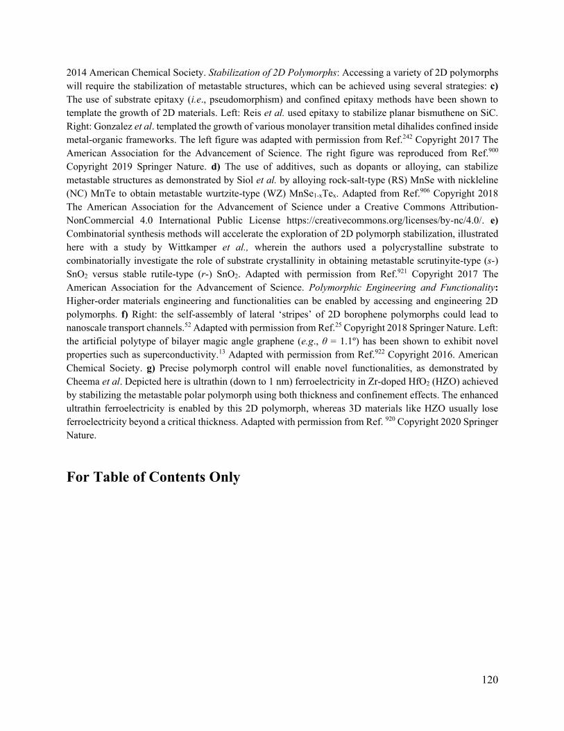
120
2014 American Chemical Society. Stabilization of 2D Polymorphs: Accessing a variety of 2D polymorphs
will require the stabilization of metastable structures, which can be achieved using several strategies: c)
The use of substrate epitaxy (i.e., pseudomorphism) and confined epitaxy methods have been shown to
template the growth of 2D materials. Left: Reis et al. used epitaxy to stabilize planar bismuthene on SiC.
Right: Gonzalez et al. templated the growth of various monolayer transition metal dihalides confined inside
metal-organic frameworks. The left figure was adapted with permission from Ref.242 Copyright 2017 The
American Association for the Advancement of Science. The right figure was reproduced from Ref.900
Copyright 2019 Springer Nature. d) The use of additives, such as dopants or alloying, can stabilize
metastable structures as demonstrated by Siol et al. by alloying rock-salt-type (RS) MnSe with nickleline
(NC) MnTe to obtain metastable wurtzite-type (WZ) MnSe1-xTex. Adapted from Ref.906 Copyright 2018
The American Association for the Advancement of Science under a Creative Commons Attribution-
NonCommercial 4.0 International Public License https://creativecommons.org/licenses/by-nc/4.0/. e)
Combinatorial synthesis methods will accelerate the exploration of 2D polymorph stabilization, illustrated
here with a study by Wittkamper et al., wherein the authors used a polycrystalline substrate to
combinatorially investigate the role of substrate crystallinity in obtaining metastable scrutinyite-type (s-)
SnO2 versus stable rutile-type (r-) SnO2. Adapted with permission from Ref.921 Copyright 2017 The
American Association for the Advancement of Science. Polymorphic Engineering and Functionality:
Higher-order materials engineering and functionalities can be enabled by accessing and engineering 2D
polymorphs. f) Right: the self-assembly of lateral ‘stripes’ of 2D borophene polymorphs could lead to
nanoscale transport channels.52 Adapted with permission from Ref.25 Copyright 2018 Springer Nature. Left:
the artificial polytype of bilayer magic angle graphene (e.g., θ = 1.1º) has been shown to exhibit novel
properties such as superconductivity.13 Adapted with permission from Ref.922 Copyright 2016. American
Chemical Society. g) Precise polymorph control will enable novel functionalities, as demonstrated by
Cheema et al. Depicted here is ultrathin (down to 1 nm) ferroelectricity in Zr-doped HfO2 (HZO) achieved
by stabilizing the metastable polar polymorph using both thickness and confinement effects. The enhanced
ultrathin ferroelectricity is enabled by this 2D polymorph, whereas 3D materials like HZO usually lose
ferroelectricity beyond a critical thickness. Adapted with permission from Ref. 920 Copyright 2020 Springer
Nature.
For Table of Contents Only
121
6. Author Information
6.1. Biographies
Dr. Hadallia Bergeron recently defended her PhD in Materials Science and Engineering
from Northwestern University under the supervision of Professor Mark Hersam. She obtained her
B.Sc in Physics from McGill University in 2013. Her research focuses on the vapor-phase
synthesis of two-dimensional metal chalcogenide semiconductors. Her efforts at understanding the
phase evolution of indium selenide helped to inspire this review.
Dr. Dmitry Lebedev is currently pursuing his postdoctoral research work in the Materials
Science and Engineering department at Northwestern University in the group of Professor Mark
Hersam. He obtained his B.Sc. and M.Sc. in Materials from Moscow State University and his PhD in
Chemistry from ETH Zurich.
Dr. Mark C. Hersam is the Walter P. Murphy Professor of Materials Science and
Engineering and Director of the Materials Research Center at Northwestern University. His
research interests include nanomaterials, scanning probe microscopy, nanoelectronic devices, and
renewable energy technologies. He has received several honors including the Presidential Early

122
Career Award for Scientists and Engineers, Materials Research Society Outstanding Young
Investigator Award, MacArthur Fellowship, U.S. Science Envoy, National Academy of Inventors,
and AVS Medard W. Welch Award.
7. Acknowledgements
This research was supported by the Materials Research Science and Engineering Center (MRSEC)
of Northwestern University (NSF DMR-1720139). H.B. acknowledges Dr. Bernard Beckerman
for his help on proofreading parts of this manuscript. D.L. would like to thank the Swiss National
Science Foundation for an Early PostDoc Mobility Fellowship (P2EZP2_181614) in addition to
the U.S. National Science Foundation (NSF DMR-2004420).
8. References
(1) Herbstein, F. H. Diversity Amidst Similarity: A Multidisciplinary Approach to Phase
Relationships, Solvates, and Polymorphs. Cryst. Growth Des. 2004, 4, 1419–1429.
(2) Davey, J. W.; Hohenlohe, P. A.; Etter, P. D.; Boone, J. Q.; Catchen, J. M.; Blaxter, M. L.
Genome-Wide Genetic Marker Discovery and Genotyping Using Next-Generation
Sequencing. Nat. Rev. Genet. 2011, 12, 499–510.
(3) Moulton, B.; Zaworotko, M. J. From Molecules to Crystal Engineering: Supramolecular
Isomerism and Polymorphism in Network Solids. Chem. Rev. 2001, 101, 1629–1658.
(4) Blagden, N.; de Matas, M.; Gavan, P. T.; York, P. Crystal Engineering of Active
Pharmaceutical Ingredients to Improve Solubility and Dissolution Rates. Adv. Drug Deliv.
Rev. 2007, 59, 617–630.
(5) Brittain, H. G. Polymorphism in Pharmaceutical Solids; CRC Press, 2016.
(6) Chandran, M. Chapter Six - Synthesis, Characterization, and Applications of Diamond
Films. In Carbon-Based Nanofillers and Their Rubber Nanocomposites; Yaragalla, S.,
Mishra, R., Thomas, S., Kalarikkal, N., Maria, H. J., Eds.; Elsevier, 2019; pp. 183–224.

123
(7) Trigunayat, G. C.; Verma, A. R. Polytypism and Stacking Faults in Crystals with Layer
Structure. In Crystallography and Crystal Chemistry of Materials with Layered Structures;
Lévy, F., Ed.; Physics and Chemistry of Materials with Layered Structures; Springer
Netherlands: Dordrecht, 1976; pp. 269–340.
(8) Boehm, H. P.; Coughlin, R. W. Enthalpy Difference of Hexagonal and Rhombohedral
Graphite. Carbon 1964, 2, 1–6.
(9) Bistritzer, R.; MacDonald, A. H. Moiré Bands in Twisted Double-Layer Graphene. Proc.
Natl. Acad. Sci. 2011, 108, 12233–12237.
(10) Suárez Morell, E.; Correa, J. D.; Vargas, P.; Pacheco, M.; Barticevic, Z. Flat Bands in
Slightly Twisted Bilayer Graphene: Tight-Binding Calculations. Phys. Rev. B 2010, 82,
121407.
(11) Cao, Y.; Fatemi, V.; Fang, S.; Tomarken, S. L.; Luo, J. Y.; Sanchez-Yamagishi, J. D.;
Watanabe, K.; Taniguchi, T.; Kaxiras, E.; et al. Correlated Insulator Behaviour at Half-
Filling in Magic-Angle Graphene Superlattices. Nature 2018, 556, 80–84.
(12) Cao, Y.; Rodan-Legrain, D.; Rubies-Bigorda, O.; Park, J. M.; Watanabe, K.; Taniguchi,
T.; Jarillo-Herrero, P. Tunable Correlated States and Spin-Polarized Phases in Twisted
Bilayer–Bilayer Graphene. Nature 2020, 583, 215–220.
(13) Cao, Y.; Fatemi, V.; Fang, S.; Watanabe, K.; Taniguchi, T.; Kaxiras, E.; Jarillo-Herrero,
P. Unconventional Superconductivity in Magic-Angle Graphene Superlattices. Nature
2018, 556, 43–50.
(14) Yankowitz, M.; Chen, S.; Polshyn, H.; Zhang, Y.; Watanabe, K.; Taniguchi, T.; Graf, D.;
Young, A. F.; Dean, C. R. Tuning Superconductivity in Twisted Bilayer Graphene. Science
2019, 363, 1059–1064.
(15) Lin, Y.; Zhang, L.; Mao, H.; Chow, P.; Xiao, Y.; Baldini, M.; Shu, J.; Mao, W. L.
Amorphous Diamond: A High-Pressure Superhard Carbon Allotrope. Phys. Rev. Lett.
2011, 107, 175504.
(16) Voiry, D.; Mohite, A.; Chhowalla, M. Phase Engineering of Transition Metal
Dichalcogenides. Chem. Soc. Rev. 2015, 44, 2702–2712.
(17) Wang, J.; Wei, Y.; Li, H.; Huang, X.; Zhang, H. Crystal Phase Control in Two-
Dimensional Materials. Sci. China Chem. 2018, 61, 1227–1242.
(18) Xiao, Y.; Zhou, M.; Liu, J.; Xu, J.; Fu, L. Phase Engineering of Two-Dimensional
Transition Metal Dichalcogenides. Sci. China Mater. 2019, 62, 759–775.
(19) Manzeli, S.; Ovchinnikov, D.; Pasquier, D.; Yazyev, O. V.; Kis, A. 2D Transition Metal
Dichalcogenides. Nat. Rev. Mater. 2017, 2, 17033.
124
(20) Yang, H.; Kim, S. W.; Chhowalla, M.; Lee, Y. H. Structural and Quantum-State Phase
Transitions in van der Waals Layered Materials. Nature Phys. 2017, 13, 931–937.
(21) Wang, X.; Song, Z.; Wen, W.; Liu, H.; Wu, J.; Dang, C.; Hossain, M.; Iqbal, M. A.; Xie,
L. Potential 2D Materials with Phase Transitions: Structure, Synthesis, and Device
Applications. Adv. Mater. 2019, 31, 1804682.
(22) Sokolikova, M. S.; Mattevi, C. Direct Synthesis of Metastable Phases of 2D Transition
Metal Dichalcogenides. Chem. Soc. Rev. 2020, 49, 3952–3980.
(23) Motizuki, Kazuko. Structural Phase Transitions in Layered Transition Metal Compounds;
Springer, 1986; Vol. 8.
(24) Rachel, S.; Ezawa, M. Giant Magnetoresistance and Perfect Spin Filter in Silicene,
Germanene, and Stanene. Phys. Rev. B 2014, 89, 195303.
(25) Liu, X.; Zhang, Z.; Wang, L.; Yakobson, B. I.; Hersam, M. C. Intermixing and Periodic
Self-Assembly of Borophene Line Defects. Nature Mater. 2018, 17, 783–788.
(26) Ramsdell, L. S. Studies on Silicon Carbide. American Mineralogist 1947, 32, 64–82.
(27) Guinier, A.; Bokij, G. B.; Boll-Dornberger, K.; Cowley, J. M.; Ďurovič, S.; Jagodzinski,
H.; Krishna, P.; de Wolff, P. M.; Zvyagin, B. B.; Cox, D. E.; et al. Nomenclature of
Polytype Structures. Report of the International Union of Crystallography Ad Hoc
Committee on the Nomenclature of Disordered, Modulated and Polytype Structures. Acta
Cryst. A 1984, 40, 399–404.
(28) Katzke, H.; Tolédano, P.; Depmeier, W. Phase Transitions between Polytypes and
Intralayer Superstructures in Transition Metal Dichalcogenides. Phys. Rev. B 2004, 69,
134111.
(29) Pałosz, B. Reasons for Polytypism of Crystals of the Type MX2 II. Clasification of Faults
and Structural Series of Polytypes; Conditions of Polytypic Growth of CdI2, PbI2, CdBr2,
SnS2, SnSe2 and Ti1.2S2. Phys. Stat. Sol. A 1983, 80, 11–41.
(30) Mannix, A. J.; Zhou, X.-F.; Kiraly, B.; Wood, J. D.; Alducin, D.; Myers, B. D.; Liu, X.;
Fisher, B. L.; Santiago, U.; Guest, J. R.; et al. Synthesis of Borophenes: Anisotropic, Two-
Dimensional Boron Polymorphs. Science 2015, 350, 1513–1516.
(31) Feng, B.; Zhang, J.; Zhong, Q.; Li, W.; Li, S.; Li, H.; Cheng, P.; Meng, S.; Chen, L.; Wu,
K. Experimental Realization of Two-Dimensional Boron Sheets. Nature Chem. 2016, 8,
563–568.
(32) Kamal, C.; Chakrabarti, A.; Ezawa, M. Aluminene as Highly Hole‐doped Graphene. New
J. Phys. 2015, 17, 083014.

125
(33) Lukačević, I.; Varga Pajtler, M.; Mužević, M.; Gupta, S. K. Prospects for Experimental
Realization of Two-Dimensional Aluminium Allotropes. J. Mater. Chem. C 2019, 7,
2666–2675.
(34) Kochat, V.; Samanta, A.; Zhang, Y.; Bhowmick, S.; Manimuda, P.; Asif, S. A. S.; Stender,
A. S.; Vajtai, R.; Singh, A. K.; Tiwary, C. S.; et al. Atomically Thin Gallium Layers from
Solid-Melt Exfoliation. Sci. Adv. 2018, 4, e1701373.
(35) Singh, D.; Gupta, S. K.; Lukačević, I.; Sonvane, Y. Indiene 2D Monolayer: A New
Nanoelectronic Material. RSC Adv. 2016, 6, 8006–8014.
(36) Mannix, A. J.; Kiraly, B.; Hersam, M. C.; Guisinger, N. P. Synthesis and Chemistry of
Elemental 2D Materials. Nat. Rev. Chem. 2017, 1, 0014.
(37) Zhang, Z.; Penev, E. S.; Yakobson, B. I. Two-Dimensional Boron: Structures, Properties
and Applications. Chem. Soc. Rev. 2017, 46, 6746–6763.
(38) Huang, Y.; Shirodkar, S. N.; Yakobson, B. I. Two-Dimensional Boron Polymorphs for
Visible Range Plasmonics: A First-Principles Exploration. J. Am. Chem. Soc. 2017, 139,
17181–17185.
(39) Mannix, A. J.; Zhang, Z.; Guisinger, N. P.; Yakobson, B. I.; Hersam, M. C. Borophene as
a Prototype for Synthetic 2D Materials Development. Nature Nanotech. 2018, 13, 444–
450.
(40) Boustani, I. Systematic Ab Initio Investigation of Bare Boron Clusters: Determination of
the Geometry and Electronic Structures of BN (N=2–14). Phys. Rev. B 1997, 55, 16426–
16438.
(41) Tang, H.; Ismail-Beigi, S. Novel Precursors for Boron Nanotubes: The Competition of
Two-Center and Three-Center Bonding in Boron Sheets. Phys. Rev. Lett. 2007, 99,
115501.
(42) Yang, X.; Ding, Y.; Ni, J. Ab Initio Prediction of Stable Boron Sheets and Boron
Nanotubes: Structure, Stability, and Electronic Properties. Phys. Rev. B 2008, 77, 041402.
(43) Wu, X.; Dai, J.; Zhao, Y.; Zhuo, Z.; Yang, J.; Zeng, X. C. Two-Dimensional Boron
Monolayer Sheets. ACS Nano 2012, 6, 7443–7453.
(44) Penev, E. S.; Bhowmick, S.; Sadrzadeh, A.; Yakobson, B. I. Polymorphism of Two-
Dimensional Boron. Nano Lett. 2012, 12, 2441–2445.
(45) Yu, X.; Li, L.; Xu, X.-W.; Tang, C.-C. Prediction of Two-Dimensional Boron Sheets by
Particle Swarm Optimization Algorithm. J. Phys. Chem. C 2012, 116, 20075–20079.
(46) Lu, H.; Mu, Y.; Bai, H.; Chen, Q.; Li, S.-D. Binary Nature of Monolayer Boron Sheets
from Ab Initio Global Searches. J. Chem. Phys. 2013, 138, 024701.

126
(47) Campbell, G. P.; Mannix, A. J.; Emery, J. D.; Lee, T.-L.; Guisinger, N. P.; Hersam, M. C.;
Bedzyk, M. J. Resolving the Chemically Discrete Structure of Synthetic Borophene
Polymorphs. Nano Lett. 2018, 18, 2816–2821.
(48) Liu, X.; Wang, L.; Li, S.; Rahn, M. S.; Yakobson, B. I.; Hersam, M. C. Geometric Imaging
of Borophene Polymorphs with Functionalized Probes. Nat. Commun. 2019, 10, 1642.
(49) Feng, B.; Zhang, J.; Liu, R.-Y.; Iimori, T.; Lian, C.; Li, H.; Chen, L.; Wu, K.; Meng, S.;
Komori, F.; et al. Direct Evidence of Metallic Bands in a Monolayer Boron Sheet. Phys.
Rev. B 2016, 94, 041408.
(50) Kiraly, B.; Liu, X.; Wang, L.; Zhang, Z.; Mannix, A. J.; Fisher, B. L.; Yakobson, B. I.;
Hersam, M. C.; Guisinger, N. P. Borophene Synthesis on Au(111). ACS Nano 2019, 13,
3816–3822.
(51) Zhong, Q.; Zhang, J.; Cheng, P.; Feng, B.; Li, W.; Sheng, S.; Li, H.; Meng, S.; Chen, L.;
u, K. Metastable Phases of 2D Boron Sheets on Ag(111). J. Phys.: Condens. Matter 2017,
29, 095002.
(52) Silvestre, G. H.; Scopel, W. L.; Miwa, R. H. Electronic Stripes and Transport Properties
in Borophene Heterostructures. Nanoscale 2019, 11, 17894–17903.
(53) Feng, B.; Sugino, O.; Liu, R.-Y.; Zhang, J.; Yukawa, R.; Kawamura, M.; Iimori, T.; Kim,
H.; Hasegawa, Y.; Li, H.; et al. Dirac Fermions in Borophene. Phys. Rev. Lett. 2017, 118,
096401.
(54) Feng, B.; Zhang, J.; Ito, S.; Arita, M.; Cheng, C.; Chen, L.; Wu, K.; Komori, G.; Sugino,
O.; Miyamoto, K.; et al. Discovery of 2D Anisotropic Dirac Cones. Adv. Mater. 2018, 30,
1704025.
(55) Gupta, S.; Kutana, A.; Yakobson, B. I. Dirac Cones and Nodal Line in Borophene. J. Phys.
Chem. Lett. 2018, 9, 2757–2762.
(56) Penev, E. S.; Kutana, A.; Yakobson, B. I. Can Two-Dimensional Boron Superconduct?
Nano Lett. 2016, 16, 2522–2526.
(57) Zhao, Y.; Zeng, S.; Ni, J. Phonon-Mediated Superconductivity in Borophenes. Appl. Phys.
Lett. 2016, 108, 242601.
(58) Gao, M.; Li, Q.-Z.; Yan, X.-W.; Wang, J. Prediction of Phonon-Mediated
Superconductivity in Borophene. Phys. Rev. B 2017, 95, 024505.
(59) Zhang, H.; Xie, Y.; Zhang, Z.; Zhong, C.; Li, Y.; Chen, Z.; Chen, Y. Dirac Nodal Lines
and Tilted Semi-Dirac Cones Coexisting in a Striped Boron Sheet. J. Phys. Chem. Lett.
2017, 8, 1707–1713.
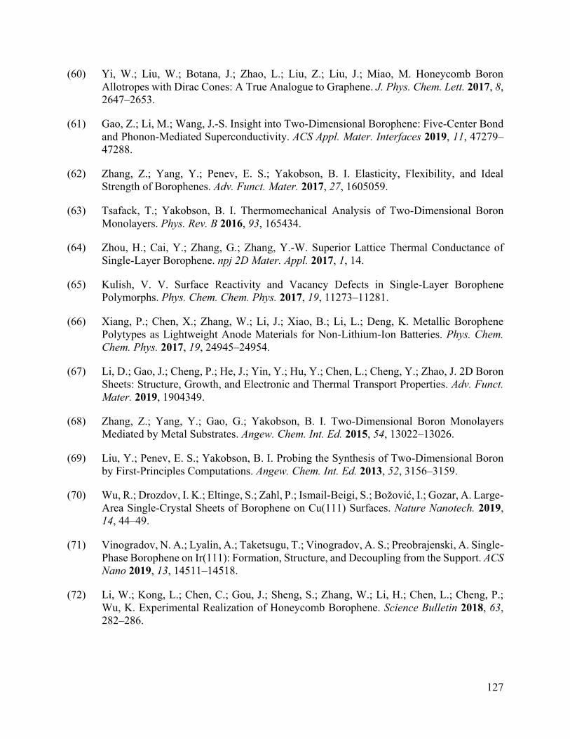
127
(60) Yi, W.; Liu, W.; Botana, J.; Zhao, L.; Liu, Z.; Liu, J.; Miao, M. Honeycomb Boron
Allotropes with Dirac Cones: A True Analogue to Graphene. J. Phys. Chem. Lett. 2017, 8,
2647–2653.
(61) Gao, Z.; Li, M.; Wang, J.-S. Insight into Two-Dimensional Borophene: Five-Center Bond
and Phonon-Mediated Superconductivity. ACS Appl. Mater. Interfaces 2019, 11, 47279–
47288.
(62) Zhang, Z.; Yang, Y.; Penev, E. S.; Yakobson, B. I. Elasticity, Flexibility, and Ideal
Strength of Borophenes. Adv. Funct. Mater. 2017, 27, 1605059.
(63) Tsafack, T.; Yakobson, B. I. Thermomechanical Analysis of Two-Dimensional Boron
Monolayers. Phys. Rev. B 2016, 93, 165434.
(64) Zhou, H.; Cai, Y.; Zhang, G.; Zhang, Y.-W. Superior Lattice Thermal Conductance of
Single-Layer Borophene. npj 2D Mater. Appl. 2017, 1, 14.
(65) Kulish, V. V. Surface Reactivity and Vacancy Defects in Single-Layer Borophene
Polymorphs. Phys. Chem. Chem. Phys. 2017, 19, 11273–11281.
(66) Xiang, P.; Chen, X.; Zhang, W.; Li, J.; Xiao, B.; Li, L.; Deng, K. Metallic Borophene
Polytypes as Lightweight Anode Materials for Non-Lithium-Ion Batteries. Phys. Chem.
Chem. Phys. 2017, 19, 24945–24954.
(67) Li, D.; Gao, J.; Cheng, P.; He, J.; Yin, Y.; Hu, Y.; Chen, L.; Cheng, Y.; Zhao, J. 2D Boron
Sheets: Structure, Growth, and Electronic and Thermal Transport Properties. Adv. Funct.
Mater. 2019, 1904349.
(68) Zhang, Z.; Yang, Y.; Gao, G.; Yakobson, B. I. Two-Dimensional Boron Monolayers
Mediated by Metal Substrates. Angew. Chem. Int. Ed. 2015, 54, 13022–13026.
(69) Liu, Y.; Penev, E. S.; Yakobson, B. I. Probing the Synthesis of Two-Dimensional Boron
by First-Principles Computations. Angew. Chem. Int. Ed. 2013, 52, 3156–3159.
(70) Wu, R.; Drozdov, I. K.; Eltinge, S.; Zahl, P.; Ismail-Beigi, S.; Božović, I.; Gozar, A. Large-
Area Single-Crystal Sheets of Borophene on Cu(111) Surfaces. Nature Nanotech. 2019,
14, 44–49.
(71) Vinogradov, N. A.; Lyalin, A.; Taketsugu, T.; Vinogradov, A. S.; Preobrajenski, A. Single-
Phase Borophene on Ir(111): Formation, Structure, and Decoupling from the Support. ACS
Nano 2019, 13, 14511–14518.
(72) Li, W.; Kong, L.; Chen, C.; Gou, J.; Sheng, S.; Zhang, W.; Li, H.; Chen, L.; Cheng, P.;
Wu, K. Experimental Realization of Honeycomb Borophene. Science Bulletin 2018, 63,
282–286.
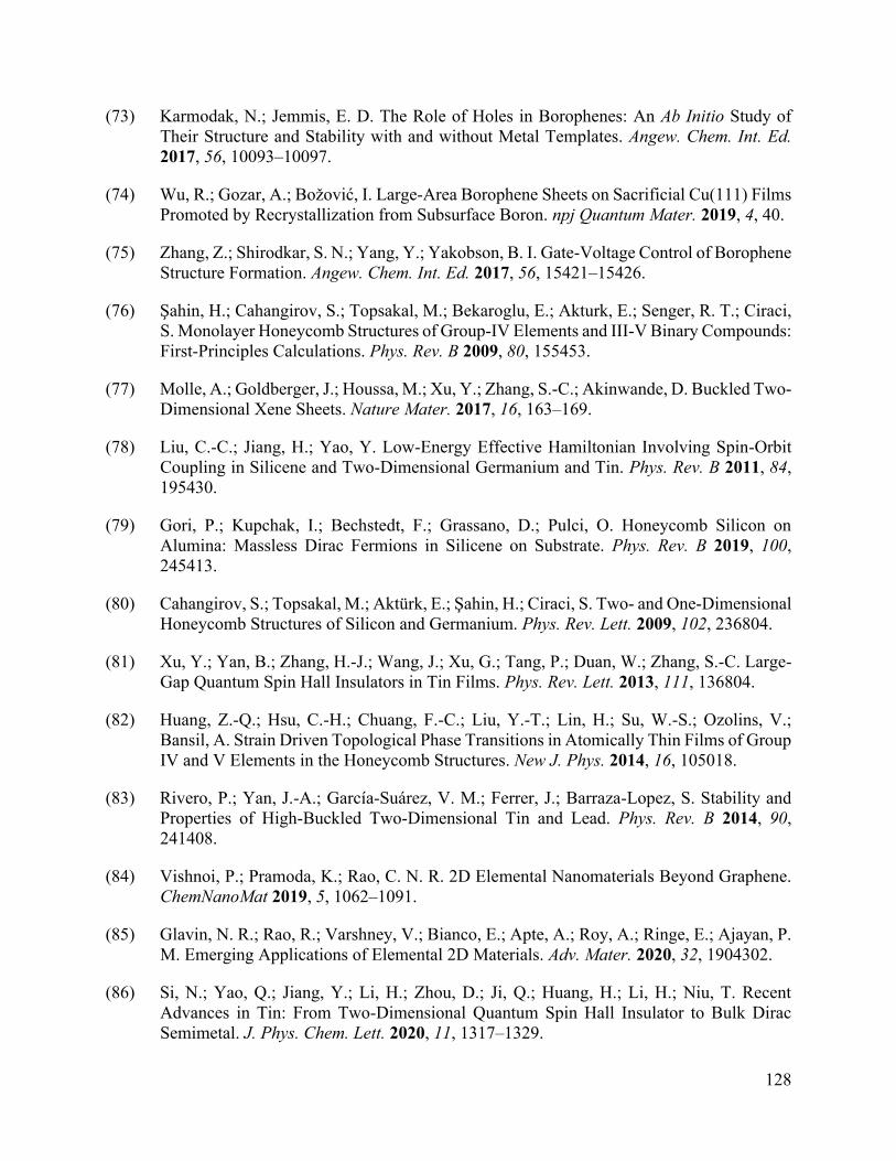
128
(73) Karmodak, N.; Jemmis, E. D. The Role of Holes in Borophenes: An Ab Initio Study of
Their Structure and Stability with and without Metal Templates. Angew. Chem. Int. Ed.
2017, 56, 10093–10097.
(74) Wu, R.; Gozar, A.; Božović, I. Large-Area Borophene Sheets on Sacrificial Cu(111) Films
Promoted by Recrystallization from Subsurface Boron. npj Quantum Mater. 2019, 4, 40.
(75) Zhang, Z.; Shirodkar, S. N.; Yang, Y.; Yakobson, B. I. Gate-Voltage Control of Borophene
Structure Formation. Angew. Chem. Int. Ed. 2017, 56, 15421–15426.
(76) Şahin, H.; Cahangirov, S.; Topsakal, M.; Bekaroglu, E.; Akturk, E.; Senger, R. T.; Ciraci,
S. Monolayer Honeycomb Structures of Group-IV Elements and III-V Binary Compounds:
First-Principles Calculations. Phys. Rev. B 2009, 80, 155453.
(77) Molle, A.; Goldberger, J.; Houssa, M.; Xu, Y.; Zhang, S.-C.; Akinwande, D. Buckled Two-
Dimensional Xene Sheets. Nature Mater. 2017, 16, 163–169.
(78) Liu, C.-C.; Jiang, H.; Yao, Y. Low-Energy Effective Hamiltonian Involving Spin-Orbit
Coupling in Silicene and Two-Dimensional Germanium and Tin. Phys. Rev. B 2011, 84,
195430.
(79) Gori, P.; Kupchak, I.; Bechstedt, F.; Grassano, D.; Pulci, O. Honeycomb Silicon on
Alumina: Massless Dirac Fermions in Silicene on Substrate. Phys. Rev. B 2019, 100,
245413.
(80) Cahangirov, S.; Topsakal, M.; Aktürk, E.; Şahin, H.; Ciraci, S. Two- and One-Dimensional
Honeycomb Structures of Silicon and Germanium. Phys. Rev. Lett. 2009, 102, 236804.
(81) Xu, Y.; Yan, B.; Zhang, H.-J.; Wang, J.; Xu, G.; Tang, P.; Duan, W.; Zhang, S.-C. Large-
Gap Quantum Spin Hall Insulators in Tin Films. Phys. Rev. Lett. 2013, 111, 136804.
(82) Huang, Z.-Q.; Hsu, C.-H.; Chuang, F.-C.; Liu, Y.-T.; Lin, H.; Su, W.-S.; Ozolins, V.;
Bansil, A. Strain Driven Topological Phase Transitions in Atomically Thin Films of Group
IV and V Elements in the Honeycomb Structures. New J. Phys. 2014, 16, 105018.
(83) Rivero, P.; Yan, J.-A.; García-Suárez, V. M.; Ferrer, J.; Barraza-Lopez, S. Stability and
Properties of High-Buckled Two-Dimensional Tin and Lead. Phys. Rev. B 2014, 90,
241408.
(84) Vishnoi, P.; Pramoda, K.; Rao, C. N. R. 2D Elemental Nanomaterials Beyond Graphene.
ChemNanoMat 2019, 5, 1062–1091.
(85) Glavin, N. R.; Rao, R.; Varshney, V.; Bianco, E.; Apte, A.; Roy, A.; Ringe, E.; Ajayan, P.
M. Emerging Applications of Elemental 2D Materials. Adv. Mater. 2020, 32, 1904302.
(86) Si, N.; Yao, Q.; Jiang, Y.; Li, H.; Zhou, D.; Ji, Q.; Huang, H.; Li, H.; Niu, T. Recent
Advances in Tin: From Two-Dimensional Quantum Spin Hall Insulator to Bulk Dirac
Semimetal. J. Phys. Chem. Lett. 2020, 11, 1317–1329.
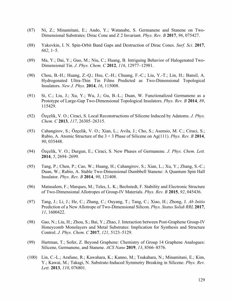
129
(87) Ni, Z.; Minamitani, E.; Ando, Y.; Watanabe, S. Germanene and Stanene on Two-
Dimensional Substrates: Dirac Cone and Z 2 Invariant. Phys. Rev. B 2017, 96, 075427.
(88) Yakovkin, I. N. Spin-Orbit Band Gaps and Destruction of Dirac Cones. Surf. Sci. 2017,
662, 1–5.
(89) Ma, Y.; Dai, Y.; Guo, M.; Niu, C.; Huang, B. Intriguing Behavior of Halogenated Two-
Dimensional Tin. J. Phys. Chem. C 2012, 116, 12977–12981.
(90) Chou, B.-H.; Huang, Z.-Q.; Hsu, C.-H.; Chuang, F.-C.; Liu, Y.-T.; Lin, H.; Bansil, A.
Hydrogenated Ultra-Thin Tin Films Predicted as Two-Dimensional Topological
Insulators. New J. Phys. 2014, 16, 115008.
(91) Si, C.; Liu, J.; Xu, Y.; Wu, J.; Gu, B.-L.; Duan, W. Functionalized Germanene as a
Prototype of Large-Gap Two-Dimensional Topological Insulators. Phys. Rev. B 2014, 89,
115429.
(92) Özçelik, V. O.; Ciraci, S. Local Reconstructions of Silicene Induced by Adatoms. J. Phys.
Chem. C 2013, 117, 26305–26315.
(93) Cahangirov, S.; Özçelik, V. O.; Xian, L.; Avila, J.; Cho, S.; Asensio, M. C.; Ciraci, S.;
Rubio, A. Atomic Structure of the 3 × 3 Phase of Silicene on Ag(111). Phys. Rev. B 2014,
90, 035448.
(94) Özçelik, V. O.; Durgun, E.; Ciraci, S. New Phases of Germanene. J. Phys. Chem. Lett.
2014, 5, 2694–2699.
(95) Tang, P.; Chen, P.; Cao, W.; Huang, H.; Cahangirov, S.; Xian, L.; Xu, Y.; Zhang, S.-C.;
Duan, W.; Rubio, A. Stable Two-Dimensional Dumbbell Stanene: A Quantum Spin Hall
Insulator. Phys. Rev. B 2014, 90, 121408.
(96) Matusalem, F.; Marques, M.; Teles, L. K.; Bechstedt, F. Stability and Electronic Structure
of Two-Dimensional Allotropes of Group-IV Materials. Phys. Rev. B 2015, 92, 045436.
(97) Tang, J.; Li, J.; He, C.; Zhang, C.; Ouyang, T.; Tang, C.; Xiao, H.; Zhong, J. Ab Initio
Prediction of a New Allotrope of Two-Dimensional Silicon. Phys. Status Solidi RRL 2017,
11, 1600422.
(98) Gao, N.; Liu, H.; Zhou, S.; Bai, Y.; Zhao, J. Interaction between Post-Graphene Group-IV
Honeycomb Monolayers and Metal Substrates: Implication for Synthesis and Structure
Control. J. Phys. Chem. C 2017, 121, 5123–5129.
(99) Hartman, T.; Sofer, Z. Beyond Graphene: Chemistry of Group 14 Graphene Analogues:
Silicene, Germanene, and Stanene. ACS Nano 2019, 13, 8566–8576.
(100) Lin, C.-L.; Arafune, R.; Kawahara, K.; Kanno, M.; Tsukahara, N.; Minamitani, E.; Kim,
Y.; Kawai, M.; Takagi, N. Substrate-Induced Symmetry Breaking in Silicene. Phys. Rev.
Lett. 2013, 110, 076801.
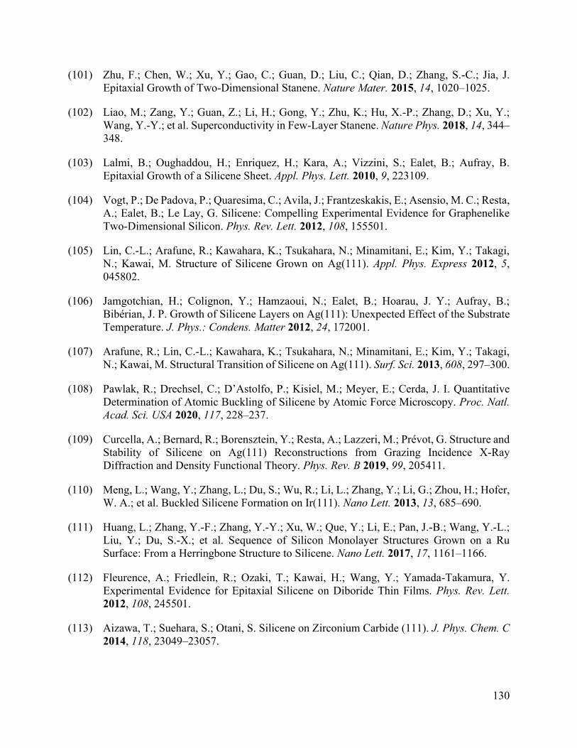
130
(101) Zhu, F.; Chen, W.; Xu, Y.; Gao, C.; Guan, D.; Liu, C.; Qian, D.; Zhang, S.-C.; Jia, J.
Epitaxial Growth of Two-Dimensional Stanene. Nature Mater. 2015, 14, 1020–1025.
(102) Liao, M.; Zang, Y.; Guan, Z.; Li, H.; Gong, Y.; Zhu, K.; Hu, X.-P.; Zhang, D.; Xu, Y.;
Wang, Y.-Y.; et al. Superconductivity in Few-Layer Stanene. Nature Phys. 2018, 14, 344–
348.
(103) Lalmi, B.; Oughaddou, H.; Enriquez, H.; Kara, A.; Vizzini, S.; Ealet, B.; Aufray, B.
Epitaxial Growth of a Silicene Sheet. Appl. Phys. Lett. 2010, 9, 223109.
(104) Vogt, P.; De Padova, P.; Quaresima, C.; Avila, J.; Frantzeskakis, E.; Asensio, M. C.; Resta,
A.; Ealet, B.; Le Lay, G. Silicene: Compelling Experimental Evidence for Graphenelike
Two-Dimensional Silicon. Phys. Rev. Lett. 2012, 108, 155501.
(105) Lin, C.-L.; Arafune, R.; Kawahara, K.; Tsukahara, N.; Minamitani, E.; Kim, Y.; Takagi,
N.; Kawai, M. Structure of Silicene Grown on Ag(111). Appl. Phys. Express 2012, 5,
045802.
(106) Jamgotchian, H.; Colignon, Y.; Hamzaoui, N.; Ealet, B.; Hoarau, J. Y.; Aufray, B.;
Bibérian, J. P. Growth of Silicene Layers on Ag(111): Unexpected Effect of the Substrate
Temperature. J. Phys.: Condens. Matter 2012, 24, 172001.
(107) Arafune, R.; Lin, C.-L.; Kawahara, K.; Tsukahara, N.; Minamitani, E.; Kim, Y.; Takagi,
N.; Kawai, M. Structural Transition of Silicene on Ag(111). Surf. Sci. 2013, 608, 297–300.
(108) Pawlak, R.; Drechsel, C.; D’Astolfo, P.; Kisiel, M.; Meyer, E.; Cerda, J. I. Quantitative
Determination of Atomic Buckling of Silicene by Atomic Force Microscopy. Proc. Natl.
Acad. Sci. USA 2020, 117, 228–237.
(109) Curcella, A.; Bernard, R.; Borensztein, Y.; Resta, A.; Lazzeri, M.; Prévot, G. Structure and
Stability of Silicene on Ag(111) Reconstructions from Grazing Incidence X-Ray
Diffraction and Density Functional Theory. Phys. Rev. B 2019, 99, 205411.
(110) Meng, L.; Wang, Y.; Zhang, L.; Du, S.; Wu, R.; Li, L.; Zhang, Y.; Li, G.; Zhou, H.; Hofer,
W. A.; et al. Buckled Silicene Formation on Ir(111). Nano Lett. 2013, 13, 685–690.
(111) Huang, L.; Zhang, Y.-F.; Zhang, Y.-Y.; Xu, W.; Que, Y.; Li, E.; Pan, J.-B.; Wang, Y.-L.;
Liu, Y.; Du, S.-X.; et al. Sequence of Silicon Monolayer Structures Grown on a Ru
Surface: From a Herringbone Structure to Silicene. Nano Lett. 2017, 17, 1161–1166.
(112) Fleurence, A.; Friedlein, R.; Ozaki, T.; Kawai, H.; Wang, Y.; Yamada-Takamura, Y.
Experimental Evidence for Epitaxial Silicene on Diboride Thin Films. Phys. Rev. Lett.
2012, 108, 245501.
(113) Aizawa, T.; Suehara, S.; Otani, S. Silicene on Zirconium Carbide (111). J. Phys. Chem. C
2014, 118, 23049–23057.

131
(114) Stȩpniak-Dybala, A.; Krawiec, M. Formation of Silicene on Ultrathin Pb(111) Films. J.
Phys. Chem. C 2019, 123, 17019–17025.
(115) Li, L.; Lu, S.; Pan, J.; Qin, Z.; Wang, Y.; Wang, Y.; Cao, G.; Du, S.; Gao, H.-J. Buckled
Germanene Formation on Pt(111). Adv. Mater. 2014, 26, 4820–4824.
(116) Dávila, M. E.; Xian, L.; Cahangirov, S.; Rubio, A.; Le Lay, G. Germanene: A Novel Two-
Dimensional Germanium Allotrope Akin to Graphene and Silicene. New J. Phys. 2014,
16, 095002.
(117) Zhuang, J.; Gao, N.; Li, Z.; Xu, X.; Wang, J.; Zhao, J.; Dou, S. X.; Du, Y. Cooperative
Electron–Phonon Coupling and Buckled Structure in Germanene on Au(111). ACS Nano
2017, 11, 3553–3559.
(118) Dávila, M. E.; Le Lay, G. Few Layer Epitaxial Germanene: A Novel Two-Dimensional
Dirac Material. Sci Rep 2016, 6, 20714.
(119) Lin, C.-H.; Huang, A.; Pai, W. W.; Chen, W.-C.; Chen, T.-Y.; Chang, T.-R.; Yukawa, R.;
Cheng, C.-M.; Mou, C.-Y.; Matsuda, I.; et al. Single-Layer Dual Germanene Phases on
Ag(111). Phys. Rev. Materials 2018, 2, 024003.
(120) Chiniwar, S.; Huang, A.; Chen, T.-Y.; Lin, C.-H.; Hsing, C.-R.; Chen, W.-C.; Cheng, C.-
M.; Jeng, H.-T.; Wei, C. M.; Pai, W. W.; et al. Substrate-Mediated Umklapp Scattering at
the Incommensurate Interface of a Monatomic Alloy Layer. Phys. Rev. B 2019, 99,
155408.
(121) Derivaz, M.; Dentel, D.; Stephan, R.; Hanf, M.-C.; Mehdaoui, A.; Sonnet, P.; Pirri, C.
Continuous Germanene Layer on Al(111). Nano Lett. 2015, 15, 2510–2516.
(122) Stephan, R.; Hanf, M. C.; Derivaz, M.; Dentel, D.; Asensio, M. C.; Avila, J.; Mehdaoui,
A.; Sonnet, P.; Pirri, C. Germanene on Al(111): Interface Electronic States and Charge
Transfer. J. Phys. Chem. C 2016, 120, 1580–1585.
(123) Endo, S.; Kubo, O.; Nakashima, N.; Iwaguma, S.; Yamamoto, R.; Kamakura, Y.; Tabata,
H.; Katayama, M. √3 × √3 Germanene on Al(111) Grown at Nearly Room Temperature.
Appl. Phys. Express 2018, 11, 019201.
(124) Qin, Z.; Pan, J.; Lu, S.; Shao, Y.; Wang, Y.; Du, S.; Gao, H.-J.; Cao, G. Direct Evidence
of Dirac Signature in Bilayer Germanene Islands on Cu(111). Adv. Mater. 2017, 29,
1606046.
(125) Gou, J.; Zhong, Q.; Sheng, S.; Li, W.; Cheng, P.; Li, H.; Chen, L.; Wu, K. Strained
Monolayer Germanene with 1 × 1 Lattice on Sb(111). 2D Mater. 2016, 3, 045005.
(126) Gou, J.; Kong, L.; Li, H.; Zhong, Q.; Li, W.; Cheng, P.; Chen, L.; Wu, K. Strain-Induced
Band Engineering in Monolayer Stanene on Sb(111). Phys. Rev. Materials 2017, 1,
054004.

132
(127) Wu, H.; Tang, J.; Liang, Q.; Shi, B.; Niu, Y.; Si, J.; Liao, Q.; Dou, W. A van der Waals
Epitaxial Growth of Ultrathin Two-Dimensional Sn Film on Graphene Covered Cu(111)
Substrate. Appl. Phys. Lett. 2019, 115, 141601.
(128) Yuhara, J.; Fujii, Y.; Nishino, K.; Isobe, N.; Nakatake, M.; Xian, L.; Rubio, A.; Le Lay,
G. Large Area Planar Stanene Epitaxially Grown on Ag(111). 2D Mater. 2018, 5, 025002.
(129) Maniraj, M.; Stadtmüller, B.; Jungkenn, D.; Düvel, M.; Emmerich, S.; Shi, W.; Stöckl, J.;
Lyu, L.; Kollamana, J.; Wei, Z.; et al. A Case Study for the Formation of Stanene on a
Metal Surface. Commun. Phys. 2019, 2, 12.
(130) Liu, Y.; Gao, N.; Zhuang, J.; Liu, C.; Wang, J.; Hao, W.; Dou, S. X.; Zhao, J.; Du, Y.
Realization of Strained Stanene by Interface Engineering. J. Phys. Chem. Lett. 2019, 10,
1558–1565.
(131) Xu, C.-Z.; Chan, Y.-H.; Chen, Y.; Chen, P.; Wang, X.; Dejoie, C.; Wong, M.-H.;
Hlevyack, J. A.; Ryu, H.; Kee, H.-Y.; et al. Elemental Topological Dirac Semimetal: α-Sn
on InSb(111). Phys. Rev. Lett. 2017, 118, 146402.
(132) Xu, C.-Z.; Chan, Y.-H.; Chen, P.; Wang, X.; Flötotto, D.; Hlevyack, J. A.; Bian, G.; Mo,
S.-K.; Chou, M.-Y.; Chiang, T.-C. Gapped Electronic Structure of Epitaxial Stanene on
InSb(111). Phys. Rev. B 2018, 97, 035122.
(133) Rogalev, V. A.; Reis, F.; Adler, F.; Bauernfeind, M.; Erhardt, J.; Kowalewski, A.; Scholz,
M. R.; Dudy, L.; Duffy, L. B.; Hesjedal, T.; et al. Tailoring the Topological Surface State
in Ultrathin α-Sn(111) Films. Phys. Rev. B 2019, 100, 245144.
(134) De Crescenzi, M.; Berbezier, I.; Scarselli, M.; Castrucci, P.; Abbarchi, M.; Ronda, A.;
Jardali, F.; Park, J.; Vach, H. Formation of Silicene Nanosheets on Graphite. ACS Nano
2016, 10, 11163–11171.
(135) Chiappe, D.; Scalise, E.; Cinquanta, E.; Grazianetti, C.; van den Broek, B.; Fanciulli, M.;
Houssa, M.; Molle, A. Two-Dimensional Si Nanosheets with Local Hexagonal Structure
on a MoS2 Surface. Adv. Mater. 2014, 26, 2096–2101.
(136) Peng, W.; Xu, T.; Diener, P.; Biadala, L.; Berthe, M.; Pi, X.; Borensztein, Y.; Curcella, A.;
Bernard, R.; Prévot, G.; et al. Resolving the Controversial Existence of Silicene and
Germanene Nanosheets Grown on Graphite. ACS Nano 2018, 12, 4754–4760.
(137) van Bremen, R.; Yao, Q.; Banerjee, S.; Cakir, D.; Oncel, N.; Zandvliet, H. J. W.
Intercalation of Si between MoS2 Layers. Beilstein J. Nanotechnol. 2017, 8, 1952–1960.
(138) Gao, J.; Zhao, J. Initial Geometries, Interaction Mechanism and High Stability of Silicene
on Ag(111) Surface. Sci. Rep. 2012, 2, 861.
(139) Chen, M. X.; Zhong, Z.; Weinert, M. Designing Substrates for Silicene and Germanene:
First-Principles Calculations. Phys. Rev. B 2016, 94, 075409.

133
(140) Sone, J.; Yamagami, T.; Nakatsuji, K.; Hirayama, H. Si Growth at Graphene Surfaces on
6H-SiC(0001) Substrates. Jpn. J. Appl. Phys. 2016, 55, 035502.
(141) Guo, Z.-X.; Furuya, S.; Iwata, J.; Oshiyama, A. Absence and Presence of Dirac Electrons
in Silicene on Substrates. Phys. Rev. B 2013, 87, 235435.
(142) Wang, Y.-P.; Cheng, H.-P. Absence of a Dirac Cone in Silicene on Ag(111): First-
Principles Density Functional Calculations with a Modified Effective Band Structure
Technique. Phys. Rev. B 2013, 87, 245430.
(143) Mahatha, S. K.; Moras, P.; Bellini, V.; Sheverdyaeva, P. M.; Struzzi, C.; Petaccia, L.;
Carbone, C. Silicene on Ag(111): A Honeycomb Lattice without Dirac Bands. Phys. Rev.
B 2014, 89, 201416.
(144) Feng, Y.; Liu, D.; Feng, B.; Liu, X.; Zhao, L.; Xie, Z.; Liu, Y.; Liang, A.; Hu, C.; Hu, Y.;
et al. Direct Evidence of Interaction-Induced Dirac Cones in a Monolayer
Silicene/Ag(111) System. Proc Natl Acad Sci USA 2016, 113, 14656–14661.
(145) Feng, B.; Zhou, H.; Feng, Y.; Liu, H.; He, S.; Matsuda, I.; Chen, L.; Schwier, E. F.;
Shimada, K.; Meng, S.; et al. Superstructure-Induced Splitting of Dirac Cones in Silicene.
Phys. Rev. Lett. 2019, 122, 196801.
(146) Wang, Y.; Li, J.; Xiong, J.; Pan, Y.; Ye, M.; Guo, Y.; Zhang, H.; Quhe, R.; Lu, J. Does the
Dirac Cone of Germanene Exist on Metal Substrates? Phys. Chem. Chem. Phys. 2016, 18
(28), 19451–19456.
(147) Mannix, A. J.; Kiraly, B.; Fisher, B. L.; Hersam, M. C.; Guisinger, N. P. Silicon Growth
at the Two-Dimensional Limit on Ag(111). ACS Nano 2014, 8, 7538–7547.
(148) Shirai, T.; Shirasawa, T.; Hirahara, T.; Fukui, N.; Takahashi, T.; Hasegawa, S. Structure
Determination of Multilayer Silicene Grown on Ag(111) Films by Electron Diffraction:
Evidence for Ag Segregation at the Surface. Phys. Rev. B 2014, 89, 241403.
(149) Borensztein, Y.; Curcella, A.; Royer, S.; Prévot, G. Silicene Multilayers on Ag(111)
Display a Cubic Diamondlike Structure and a √ 3 × √ 3 Reconstruction Induced by
Surfactant Ag Atoms. Phys. Rev. B 2015, 92, 155407.
(150) Kawahara, K.; Shirasawa, T.; Lin, C.-L.; Nagao, R.; Tsukahara, N.; Takahashi, T.;
Arafune, R.; Kawai, M.; Takagi, N. Atomic Structure of “Multilayer Silicene” Grown on
Ag(111): Dynamical Low Energy Electron Diffraction Analysis. Surf. Sci. 2016, 651, 70–
75.
(151) Curcella, A.; Bernard, R.; Borensztein, Y.; Lazzeri, M.; Prévot, G. The Mechanism for the
Stabilization and Surfactant Properties of Epitaxial Silicene. Nanoscale 2018, 10, 2291–
2300.
134
(152) Yabuoshi, K.; Sugimoto, Y. Evidence for Honeycomb-Chained Trimer Structure of
Multilayer Silicene on Ag(111) with Noncontact Atomic Force Microscopy. Jpn. J. Appl.
Phys. 2019, 58, 020903.
(153) Svec, M.; Hapala, P.; Ondráček, M.; Merino, P.; Blanco-Rey, M.; Mutombo, P.;
Vondráček, M.; Polyak, Y.; Cháb, V.; Martín Gago, J. A.; et al. Silicene versus Two-
Dimensional Ordered Silicide: Atomic and Electronic Structure of Si-(19 × 19)
R23.4°/Pt(111). Phys. Rev. B 2014, 89, 201412.
(154) Ho, C.-S.; Banerjee, S.; Batzill, M.; Beck, D. E.; Koel, B. E. Formation and Structure of a
(√19×√19)R23.4°-Ge/Pt(111) Surface Alloy. Surf. Sci. 2009, 603, 1161–1167.
(155) Wang, W.; Uhrberg, R. I. G. Investigation of the Atomic and Electronic Structures of
Highly Ordered Two-Dimensional Germanium on Au(111). Phys. Rev. Materials 2017, 1,
074002.
(156) Cantero, E. D.; Solis, L. M.; Tong, Y.; Fuhr, J. D.; Martiarena, M. L.; Grizzi, O.; Sánchez,
E. A. Growth of Germanium on Au(111): Formation of Germanene or Intermixing of Au
and Ge Atoms? Phys. Chem. Chem. Phys. 2017, 19, 18580–18586.
(157) Martínez, E. A.; Fuhr, J. D.; Grizzi, O.; Sánchez, E. A.; Cantero, E. D. Growth of
Germanene on Al(111) Hindered by Surface Alloy Formation. J. Phys. Chem. C 2019,
123, 12910–12918.
(158) Muzychenko, D. A.; Oreshkin, S. I.; Panov, V. I.; Van Haesendonck, C.; Oreshkin, A. I.
Single and Multi Domain Buckled Germanene Phases on Al(111) Surface. Nano Res.
2019, 12, 2988–2996.
(159) Fang, J.; Zhao, P.; Chen, G. Germanene Growth on Al(111): A Case Study of Interface
Effect. J. Phys. Chem. C 2018, 122, 18669–18681.
(160) Luh, D.-A.; Wang, C.-H.; Yang, Y.-W. Growth of Thin Sn Films on Ag(111) Studied with
Low-Energy Electron Diffraction and X-Ray Photoelectron Spectroscopy. Thin Solid
Films 2019, 682, 44–49.
(161) Deng, J.; Xia, B.; Ma, X.; Chen, H.; Shan, H.; Zhai, X.; Li, B.; Zhao, A.; Xu, Y.; Duan,
W.; et al. Epitaxial Growth of Ultraflat Stanene with Topological Band Inversion. Nature
Mater. 2018, 17, 1081–1086.
(162) Guo, Z.-X.; Furuya, S.; Iwata, J.; Oshiyama, A. Absence of Dirac Electrons in Silicene on
Ag(111) Surfaces. J. Phys. Soc. Jpn. 2013, 82, 063714.
(163) Kokott, S.; Pflugradt, P.; Matthes, L.; Bechstedt, F. Nonmetallic Substrates for Growth of
Silicene: An Ab Initio Prediction. J. Phys.: Condens. Matter 2014, 26, 185002.
(164) Cai, Y.; Chuu, C.-P.; Wei, C. M.; Chou, M. Y. Stability and Electronic Properties of Two-
Dimensional Silicene and Germanene on Graphene. Phys. Rev. B 2013, 88, 245408.

135
(165) Matusalem, F.; Koda, D. S.; Bechstedt, F.; Marques, M.; Teles, L. K. Deposition of
Topological Silicene, Germanene and Stanene on Graphene-Covered SiC Substrates. Sci
Rep 2017, 7, 15700.
(166) Li, L.; Zhao, M. First-Principles Identifications of Superstructures of Germanene on
Ag(111) Surface and h-BN Substrate. Phys. Chem. Chem. Phys. 2013, 15, 16853.
(167) Hsu, C.-H.; Fang, Y.; Wu, S.; Huang, Z.-Q.; Crisostomo, C. P.; Gu, Y.-M.; Zhu, Z.-Z.;
Lin, H.; Bansil, A.; Chuang, F.-C.; et al. Quantum Anomalous Hall Insulator Phase in
Asymmetrically Functionalized Germanene. Phys. Rev. B 2017, 96, 165426.
(168) Galbiati, M.; Motta, N.; De Crescenzi, M.; Camilli, L. Group-IV 2D Materials beyond
Graphene on Nonmetal Substrates: Challenges, Recent Progress, and Future Perspectives.
Appl. Phys. Rev. 2019, 6, 041310.
(169) Acun, A.; Poelsema, B.; Zandvliet, H. J. W.; van Gastel, R. The Instability of Silicene on
Ag(111). Appl. Phys. Lett. 2013, 103, 263119.
(170) De Padova, P.; Generosi, A.; Paci, B.; Ottaviani, C.; Quaresima, C.; Olivieri, B.; Salomon,
E.; Angot, T.; Le Lay, G. Multilayer Silicene: Clear Evidence. 2D Mater. 2016, 3, 031011.
(171) Feng, B.; Ding, Z.; Meng, S.; Yao, Y.; He, X.; Cheng, P.; Chen, L.; Wu, K. Evidence of
Silicene in Honeycomb Structures of Silicon on Ag(111). Nano Lett. 2012, 12, 3507–3511.
(172) Zang, Y.; Jiang, T.; Gong, Y.; Guan, Z.; Liu, C.; Liao, M.; Zhu, K.; Li, Z.; Wang, L.; Li,
W.; et al. Realizing an Epitaxial Decorated Stanene with an Insulating Bandgap. Adv.
Funct. Mater. 2018, 28, 1802723.
(173) Grazianetti, C.; Chiappe, D.; Cinquanta, E.; Tallarida, G.; Fanciulli, M.; Molle, A.
Exploring the Morphological and Electronic Properties of Silicene Superstructures. Appl.
Surf. Sci. 2014, 291, 109–112.
(174) Huang, C.; Zhou, J.; Wu, H.; Deng, K.; Jena, P.; Kan, E. Quantum Phase Transition in
Germanene and Stanene Bilayer: From Normal Metal to Topological Insulator. J. Phys.
Chem. Lett. 2016, 7, 1919–1924.
(175) Zhang, W. X.; Dong, M. M.; He, C. Novel Electronic and Planar Magnetic Properties of
Two-Dimensional Surface Decorated Antimonene. Mater. Res. Bull. 2019, 118, 110489.
(176) Hsu, C.-H.; Huang, Z.-Q.; Chuang, F.-C.; Kuo, C.-C.; Liu, Y.-T.; Lin, H.; Bansil, A. The
Nontrivial Electronic Structure of Bi/Sb Honeycombs on SiC(0001). New J. Phys. 2015,
17, 025005.
(177) Zhang, S.; Hu, Y.; Hu, Z.; Cai, B.; Zeng, H. Hydrogenated Arsenenes as Planar Magnet
and Dirac Material. Appl. Phys. Lett. 2015, 107, 022102.
(178) Hsu, C.-H.; Huang, Z.-Q.; Crisostomo, C. P.; Yao, L.-Z.; Chuang, F.-C.; Liu, Y.-T.; Wang,
B.; Hsu, C.-H.; Lee, C.-C.; Lin, H.; et al. Two-Dimensional Topological Crystalline
136
Insulator Phase in Sb/Bi Planar Honeycomb with Tunable Dirac Gap. Sci Rep 2016, 6,
18993.
(179) Fu, L. Topological Crystalline Insulators. Phys. Rev. Lett. 2011, 106, 106802.
(180) Needs, R. J.; Martin, R. M.; Nielsen, O. H. Total-Energy Calculations of the Structural
Properties of the Group-V Element Arsenic. Phys. Rev. B 1986, 33, 3778–3784.
(181) Burdett, J. K.; Lee, S. Peierls Distortions in Two and Three Dimensions and the Structures
of AB Solids. J. Am. Chem. Soc. 1983, 105, 1079–1083.
(182) Gunton, D. J.; Saunders, G. A. The Young’s Modulus and Poisson’s Ratio of Arsenic,
Antimony and Bismuth. J Mater Sci 1972, 7, 1061–1068.
(183) Sturala, J.; Sofer, Z.; Pumera, M. Chemistry of Layered Pnictogens: Phosphorus, Arsenic,
Antimony, and Bismuth. Angew. Chem. 2019, 131, 7631–7637.
(184) Boulfelfel, S. E.; Seifert, G.; Grin, Y.; Leoni, S. Squeezing Lone Pairs: The A 17 to A 7
Pressure-Induced Phase Transition in Black Phosphorus. Phys. Rev. B 2012, 85, 014110.
(185) Zhang, S.; Xie, M.; Li, F.; Yan, Z.; Li, Y.; Kan, E.; Liu, W.; Chen, Z.; Zeng, H.
Semiconducting Group 15 Monolayers: A Broad Range of Band Gaps and High Carrier
Mobilities. Angew. Chem. Int. Ed. 2016, 55, 1666–1669.
(186) Ersan, F.; Aktürk, E.; Ciraci, S. Stable Single-Layer Structure of Group-V Elements. Phys.
Rev. B 2016, 94, 245417.
(187) Lin, W.; Li, J.; Wang, W.; Liang, S.-D.; Yao, D.-X. Electronic Structure and Band Gap
Engineering of Two-Dimensional Octagon-Nitrogene. Sci Rep 2018, 8, 1674.
(188) Zhang, Y.; Lee, J.; Wang, W.-L.; Yao, D.-X. Two-Dimensional Octagon-Structure
Monolayer of Nitrogen Group Elements and the Related Nano-Structures. Comput. Mater.
Sci. 2015, 110, 109–114.
(189) Carrete, J.; Gallego, L. J.; Mingo, N. Structural Complexity and Phonon Physics in 2D
Arsenenes. J. Phys. Chem. Lett. 2017, 8, 1375–1380.
(190) Kou, L.; Tan, X.; Ma, Y.; Tahini, H.; Zhou, L.; Sun, Z.; Aijun, D.; Chen, C.; Smith, S. C.
Tetragonal Bismuth Bilayer: A Stable and Robust Quantum Spin Hall Insulator. 2D Mater.
2015, 2, 045010.
(191) Eremets, M. I.; Gavriliuk, A. G.; Trojan, I. A.; Dzivenko, D. A.; Boehler, R. Single-Bonded
Cubic Form of Nitrogen. Nature Mater. 2004, 3, 558–563.
(192) Özçelik, V. O.; Aktürk, O. Ü.; Durgun, E.; Ciraci, S. Prediction of a Two-Dimensional
Crystalline Structure of Nitrogen Atoms. Phys. Rev. B 2015, 92, 125420.
137
(193) Harada, Y.; Yamamoto, M.; Baba, T.; Kita, T. Epitaxial Two-Dimensional Nitrogen
Atomic Sheet in GaAs. Appl. Phys. Lett. 2014, 104, 041907.
(194) Gusmão, R.; Sofer, Z.; Pumera, M. Black Phosphorus Rediscovered: From Bulk Material
to Monolayers. Angew. Chem. Int. Ed. 2017, 56, 8052–8072.
(195) Liu, H.; Neal, A. T.; Zhu, Z.; Luo, Z.; Xu, X.; Tománek, D.; Ye, P. D. Phosphorene: An
Unexplored 2D Semiconductor with a High Hole Mobility. ACS Nano 2014, 8, 4033–4041.
(196) Lu, W.; Nan, H.; Hong, J.; Chen, Y.; Zhu, C.; Liang, Z.; Ma, X.; Ni, Z.; Jin, C.; Zhang, Z.
Plasma-Assisted Fabrication of Monolayer Phosphorene and Its Raman Characterization.
Nano Res. 2014, 7, 853–859.
(197) Castellanos-Gomez, A.; Vicarelli, L.; Prada, E.; Island, J. O.; Narasimha-Acharya, K. L.;
Blanter, S. I.; Groenendijk, D. J.; Buscema, M.; Steele, G. A.; Alvarez, J. V.; et al. Isolation
and Characterization of Few-Layer Black Phosphorus. 2D Mater. 2014, 1, 025001.
(198) Jamieson, J. C. Crystal Structures Adopted by Black Phosphorus at High Pressures.
Science 1963, 139, 1291–1292.
(199) Zhu, Z.; Tománek, D. Semiconducting Layered Blue Phosphorus: A Computational Study.
Phys. Rev. Lett. 2014, 112, 176802.
(200) Zhang, J. L.; Zhao, S.; Han, C.; Wang, Z.; Zhong, S.; Sun, S.; Guo, R.; Zhou, X.; Gu, C.
D.; Yuan, K. D.; et al. Epitaxial Growth of Single Layer Blue Phosphorus: A New Phase
of Two-Dimensional Phosphorus. Nano Lett. 2016, 16, 4903–4908.
(201) Zhao, S.; Zhang, J. L.; Chen, W.; Li, Z. Structure of Blue Phosphorus Grown on Au(111)
Surface Revisited. J. Phys. Chem. C 2020, 124, 2024–2029.
(202) Guan, J.; Zhu, Z.; Tománek, D. Phase Coexistence and Metal-Insulator Transition in Few-
Layer Phosphorene: A Computational Study. Phys. Rev. Lett. 2014, 113, 046804.
(203) Guan, J.; Zhu, Z.; Tománek, D. Tiling Phosphorene. ACS Nano 2014, 8, 12763–12768.
(204) Wu, M.; Fu, H.; Zhou, L.; Yao, K.; Zeng, X. C. Nine New Phosphorene Polymorphs with
Non-Honeycomb Structures: A Much Extended Family. Nano Lett. 2015, 15, 3557–3562.
(205) Zhao, T.; He, C. Y.; Ma, S. Y.; Zhang, K. W.; Peng, X. Y.; Xie, G. F.; Zhong, J. X. A New
Phase of Phosphorus: The Missed Tricycle Type Red Phosphorene. J. Phys.: Condens.
Matter 2015, 27, 265301.
(206) Han, W. H.; Kim, S.; Lee, I.-H.; Chang, K. J. Prediction of Green Phosphorus with Tunable
Direct Band Gap and High Mobility. J. Phys. Chem. Lett. 2017, 8, 4627–4632.
(207) Geng, W.; Xiao, J.; Brown, J. J.; Page, A. J.; Ke, Z. New Phosphorene by Phase
Combination with Tunable Electronic and Mechanical Properties. J. Phys. Chem. C 2019,
123, 10788–10794.
138
(208) Qiu, L.; Dong, J.; Ding, F. Highly Stable Phosphorene Isomers Based on a Buckled
Honeycomb Lattice. Nanoscale 2019, 11, 7135–7139.
(209) Iwasaki, H.; Kikegawa, T. Structural Systematics of the High-Pressure Phases of
Phosphorus, Arsenic, Antimony and Bismuth. Acta Crystallogr. B Struct. Sci. 1997, 53,
353–357.
(210) Pumera, M.; Sofer, Z. 2D Monoelemental Arsenene, Antimonene, and Bismuthene:
Beyond Black Phosphorus. Adv. Mater. 2017, 29, 1605299.
(211) Osters, O.; Nilges, T.; Bachhuber, F.; Pielnhofer, F.; Weihrich, R.; Schöneich, M.;
Schmidt, P. Synthesis and Identification of Metastable Compounds: Black Arsenic-
Science or Fiction? Angew. Chem. Int. Ed. 2012, 51, 2994–2997.
(212) Zhang, Z.; Xie, J.; Yang, D.; Wang, Y.; Si, M.; Xue, D. Manifestation of Unexpected
Semiconducting Properties in Few-Layer Orthorhombic Arsenene. Appl. Phys. Express
2015, 8, 055201.
(213) Kamal, C.; Ezawa, M. Arsenene: Two-Dimensional Buckled and Puckered Honeycomb
Arsenic Systems. Phys. Rev. B 2015, 91, 085423.
(214) Kecik, D.; Durgun, E.; Ciraci, S. Stability of Single-Layer and Multilayer Arsenene and
Their Mechanical and Electronic Properties. Phys. Rev. B 2016, 94, 205409.
(215) Aktürk, O. Ü.; Özçelik, V. O.; Ciraci, S. Single-Layer Crystalline Phases of Antimony:
Antimonenes. Phys. Rev. B 2015, 91, 235446.
(216) Wang, G.; Pandey, R.; Karna, S. P. Atomically Thin Group V Elemental Films: Theoretical
Investigations of Antimonene Allotropes. ACS Appl. Mater. Interfaces 2015, 7, 11490–
11496.
(217) Cheng, L.; Liu, H.; Tan, X.; Zhang, J.; Wei, J.; Lv, H.; Shi, J.; Tang, X. Thermoelectric
Properties of a Monolayer Bismuth. J. Phys. Chem. C 2014, 118, 904–910.
(218) Aktürk, E.; Aktürk, O. Ü.; Ciraci, S. Single and Bilayer Bismuthene: Stability at High
Temperature and Mechanical and Electronic Properties. Phys. Rev. B 2016, 94, 014115.
(219) Lu, Y.; Xu, W.; Zeng, M.; Yao, G.; Shen, L.; Yang, M.; Luo, Z.; Pan, F.; Wu, K.; Das, T.;
et al. Topological Properties Determined by Atomic Buckling in Self-Assembled Ultrathin
Bi(110). Nano Lett. 2015, 15, 80–87.
(220) Kowalczyk, P. J.; Brown, S. A.; Maerkl, T.; Lu, Q.; Chiu, C.-K.; Liu, Y.; Yang, S. A.;
Wang, X.; Zasada, I.; Genuzio, F.; et al. Realization of Symmetry-Enforced Two-
Dimensional Dirac Fermions in Nonsymmorphic α-Bismuthene. ACS Nano 2020, 14,
1888–1894.
139
(221) Huang, Z.-Q.; Chuang, F.-C.; Hsu, C.-H.; Liu, Y.-T.; Chang, H.-R.; Lin, H.; Bansil, A.
Nontrivial Topological Electronic Structures in a Single Bi(111) Bilayer on Different
Substrates: A First-Principles Study. Phys. Rev. B 2013, 88, 165301.
(222) Qiao, J.; Kong, X.; Hu, Z.-X.; Yang, F.; Ji, W. High-Mobility Transport Anisotropy and
Linear Dichroism in Few-Layer Black Phosphorus. Nat. Commun. 2014, 5, 4475.
(223) Fei, R.; Faghaninia, A.; Soklaski, R.; Yan, J.-A.; Lo, C.; Yang, L. Enhanced
Thermoelectric Efficiency via Orthogonal Electrical and Thermal Conductances in
Phosphorene. Nano Lett. 2014, 14, 6393–6399.
(224) Zeraati, M.; Vaez Allaei, S. M.; Abdolhosseini Sarsari, I.; Pourfath, M.; Donadio, D.
Highly Anisotropic Thermal Conductivity of Arsenene: An Ab Initio Study. Phys. Rev. B
2016, 93, 085424.
(225) Yuan, H.; Liu, X.; Afshinmanesh, F.; Li, W.; Xu, G.; Sun, J.; Lian, B.; Curto, A. G.; Ye,
G.; Hikita, Y.; et al. Polarization-Sensitive Broadband Photodetector Using a Black
Phosphorus Vertical p–n Junction. Nature Nanotech. 2015, 10, 707–713.
(226) Wang, X.; Jones, A. M.; Seyler, K. L.; Tran, V.; Jia, Y.; Zhao, H.; Wang, H.; Yang, L.;
Xu, X.; Xia, F. Highly Anisotropic and Robust Excitons in Monolayer Black Phosphorus.
Nature Nanotech. 2015, 10, 517–521.
(227) Liu, X.; Ryder, C. R.; Wells, S. A.; Hersam, M. C. Resolving the In-Plane Anisotropic
Properties of Black Phosphorus. Small Methods 2017, 1, 1700143.
(228) Chen, Y.; Chen, C.; Kealhofer, R.; Liu, H.; Yuan, Z.; Jiang, L.; Suh, J.; Park, J.; Ko, C.;
Choe, H. S.; et al. Black Arsenic: A Layered Semiconductor with Extreme In-Plane
Anisotropy. Adv. Mater. 2018, 30, 1800754.
(229) Chen, K.-X.; Lyu, S.-S.; Wang, X.-M.; Fu, Y.-X.; Heng, Y.; Mo, D.-C. Excellent
Thermoelectric Performance Predicted in Two-Dimensional Buckled Antimonene: A
First-Principles Study. J. Phys. Chem. C 2017, 121, 13035–13042.
(230) Xiao, J.; Long, M.; Zhang, X.; Ouyang, J.; Xu, H.; Gao, Y. Theoretical Predictions on the
Electronic Structure and Charge Carrier Mobility in 2D Phosphorus Sheets. Sci. Rep. 2015,
5, 9961.
(231) Wang, Y.; Huang, P.; Ye, M.; Quhe, R.; Pan, Y.; Zhang, H.; Zhong, H.; Shi, J.; Lu, J.
Many-Body Effect, Carrier Mobility, and Device Performance of Hexagonal Arsenene and
Antimonene. Chem. Mater. 2017, 29, 2191–2201.
(232) Chowdhury, C.; Datta, A. Exotic Physics and Chemistry of Two-Dimensional Phosphorus:
Phosphorene. J. Phys. Chem. Lett. 2017, 8, 2909–2916.
(233) Xiao, C.; Wang, F.; Yang, S. A.; Lu, Y.; Feng, Y.; Zhang, S. Elemental Ferroelectricity
and Antiferroelectricity in Group-V Monolayer. Adv. Funct. Mater. 2018, 28, 1707383.
140
(234) Guo, Y.; Zhu, H.; Wang, Q. Large Second Harmonic Generation in Elemental α-Sb and α-
Bi Monolayers. J. Phys. Chem. C 2020, 124, 5506–5513.
(235) Wada, M.; Murakami, S.; Freimuth, F.; Bihlmayer, G. Localized Edge States in Two-
Dimensional Topological Insulators: Ultrathin Bi Films. Phys. Rev. B 2011, 83, 121310.
(236) Liu, Z.; Liu, C.-X.; Wu, Y.-S.; Duan, W.-H.; Liu, F.; Wu, J. Stable Nontrivial Z 2 Topology
in Ultrathin Bi(111) Films: A First-Principles Study. Phys. Rev. Lett. 2011, 107, 136805.
(237) Chen, L.; Wang, Z. F.; Liu, F. Robustness of Two-Dimensional Topological Insulator
States in Bilayer Bismuth against Strain and Electrical Field. Phys. Rev. B 2013, 87,
235420.
(238) Wang, Y.; Zhang, C.; Ji, W.; Zhang, R.; Li, P.; Wang, P.; Ren, M.; Chen, X.; Yuan, M.
Tunable Quantum Spin Hall Effect via Strain in Two-Dimensional Arsenene Monolayer.
J. Phys. D: Appl. Phys. 2016, 49, 055305.
(239) Zhang, H.; Ma, Y.; Chen, Z. Quantum Spin Hall Insulators in Strain-Modified Arsenene.
Nanoscale 2015, 7, 19152–19159.
(240) Zhao, M.; Zhang, X.; Li, L. Strain-Driven Band Inversion and Topological Aspects in
Antimonene. Sci. Rep. 2015, 5, 16108.
(241) Hu, Z.; Gao, J.; Zhang, S.; Zhao, J.; Zhou, W.; Zeng, H. Topologically Protected States
and Half-Metal Behaviors: Defect-Strain Synergy Effects in Two-Dimensional
Antimonene. Phys. Rev. Materials 2019, 3, 074005.
(242) Reis, F.; Li, G.; Dudy, L.; Bauernfeind, M.; Glass, S.; Hanke, W.; Thomale, R.; Schäfer,
J.; Claessen, R. Bismuthene on a SiC Substrate: A Candidate for a High-Temperature
Quantum Spin Hall Material. Science 2017, 357, 287–290.
(243) Sun, H.-H.; Wang, M.-X.; Zhu, F.; Wang, G.-Y.; Ma, H.-Y.; Xu, Z.-A.; Liao, Q.; Lu, Y.;
Gao, C.-L.; Li, Y.-Y.; et al. Coexistence of Topological Edge State and Superconductivity
in Bismuth Ultrathin Film. Nano Lett. 2017, 17, 3035–3039.
(244) Zhu, S.-Y.; Shao, Y.; Wang, E.; Cao, L.; Li, X.-Y.; Liu, Z.-L.; Liu, C.; Liu, L.-W.; Wang,
J.-O.; Ibrahim, K.; et al. Evidence of Topological Edge States in Buckled Antimonene
Monolayers. Nano Lett. 2019, 19, 6323–6329.
(245) Mi, K.; Xie, J.; Si, M. S.; Gao, C. X. Layer-Stacking Effect on Electronic Structures of
Bilayer Arsenene. EPL 2017, 117, 27002.
(246) Kadioglu, Y.; Santana, J. A.; Özaydin, H. D.; Ersan, F.; Aktürk, O. Ü.; Aktürk, E.;
Reboredo, F. A. Diffusion Quantum Monte Carlo and Density Functional Calculations of
the Structural Stability of Bilayer Arsenene. J. Chem. Phys. 2018, 148, 214706.

141
(247) Zhang, S.; Guo, S.; Chen, Z.; Wang, Y.; Gao, H.; Gómez-Herrero, J.; Ares, P.; Zamora,
F.; Zhu, Z.; Zeng, H. Recent Progress in 2D Group-VA Semiconductors: From Theory to
Experiment. Chem. Soc. Rev. 2018, 47, 982–1021.
(248) Ersan, F.; Kecik, D.; Özçelik, V. O.; Kadioglu, Y.; Aktürk, O. Ü.; Durgun, E.; Aktürk, E.;
Ciraci, S. Two-Dimensional Pnictogens: A Review of Recent Progresses and Future
Research Directions. Appl. Phys. Rev. 2019, 6, 021308.
(249) Wu, Z.; Hao, J. Electrical Transport Properties in Group-V Elemental Ultrathin 2D Layers.
npj 2D Mater. Appl. 2020, 4, 4.
(250) Zhuang, J.; Liu, C.; Gao, Q.; Liu, Y.; Feng, H.; Xu, X.; Wang, J.; Zhao, J.; Dou, S. X.; Hu,
Z.; et al. Band Gap Modulated by Electronic Superlattice in Blue Phosphorene. ACS Nano
2018, 12, 5059–5065.
(251) Lange, S.; Schmidt, P.; Nilges, T. Au3SnP7@Black Phosphorus: An Easy Access to Black
Phosphorus. Inorg. Chem. 2007, 46, 4028–4035.
(252) Akahama, Y.; Endo, S.; Narita, S. Electrical Properties of Black Phosphorus Single
Crystals. J. Phys. Soc. Jpn. 1983, 52, 2148–2155.
(253) Liang, L.; Wang, J.; Lin, W.; Sumpter, B. G.; Meunier, V.; Pan, M. Electronic Bandgap
and Edge Reconstruction in Phosphorene Materials. Nano Lett. 2014, 14, 6400–6406.
(254) Schiferl, D.; Barrett, C. S. The Crystal Structure of Arsenic at 4.2, 78 and 299°K. J. Appl.
Crystallogr. 1969, 2, 30–36.
(255) Kecik, D.; Özçelik, V. O.; Durgun, E.; Ciraci, S. Structure Dependent Optoelectronic
Properties of Monolayer Antimonene, Bismuthene and Their Binary Compound. Phys.
Chem. Chem. Phys. 2019, 21, 7907–7917.
(256) Cucka, P.; Barrett, C. S. The Crystal Structure of Bi and of Solid Solutions of Pb, Sn, Sb
and Te in Bi. Acta Cryst. 1962, 15, 865–872.
(257) Smith, J. B.; Hagaman, D.; Ji, H.-F. Growth of 2D Black Phosphorus Film from Chemical
Vapor Deposition. Nanotechnology 2016, 27, 215602.
(258) Li, X.; Deng, B.; Wang, X.; Chen, S.; Vaisman, M.; Karato, S.; Pan, G.; Larry Lee, M.;
Cha, J.; Wang, H.; et al. Synthesis of Thin-Film Black Phosphorus on a Flexible Substrate.
2D Mater. 2015, 2, 031002.
(259) Li, C.; Wu, Y.; Deng, B.; Xie, Y.; Guo, Q.; Yuan, S.; Chen, X.; Bhuiyan, M.; Wu, Z.;
Watanabe, K.; et al. Synthesis of Crystalline Black Phosphorus Thin Film on Sapphire.
Adv. Mater. 2018, 30, 1703748.
(260) Rajabali, M.; Esfandiari, M.; Asgharian, H.; Mohajerzadeh, S. Evolution of Phosphorene
Sheets through Direct Crystallization of Thin‐Film Red Phosphorus. Phys. Status Solidi
RRL 2019, 1900432.
142
(261) Zhang, W.; Enriquez, H.; Tong, Y.; Bendounan, A.; Kara, A.; Seitsonen, A. P.; Mayne, A.
J.; Dujardin, G.; Oughaddou, H. Epitaxial Synthesis of Blue Phosphorene. Small 2018, 14,
1804066.
(262) Hu, Y.; Qi, Z.-H.; Lu, J.; Chen, R.; Zou, M.; Chen, T.; Zhang, W.; Wang, Y.; Xue, X.; Ma,
J.; et al. Van der Waals Epitaxial Growth and Interfacial Passivation of Two-Dimensional
Single-Crystalline Few-Layer Gray Arsenic Nanoflakes. Chem. Mater. 2019, 31, 4524–
4535.
(263) Shah, J.; Wang, W.; Sohail, H. M.; Uhrberg, R. I. G. Experimental Evidence of Monolayer
Arsenene: An Exotic Two-Dimensional Semiconducting Material. 2D Mater. 2019, 7,
025013.
(264) Antonatos, N.; Luxa, J.; Sturala, J.; Sofer, Z. Black Arsenic: A New Synthetic Method by
Catalytic Crystallization of Arsenic Glass. Nanoscale 2020, 12, 5397–5401.
(265) Zhong, M.; Xia, Q.; Pan, L.; Liu, Y.; Chen, Y.; Deng, H.-X.; Li, J.; Wei, Z. Thickness-
Dependent Carrier Transport Characteristics of a New 2D Elemental Semiconductor:
Black Arsenic. Adv. Funct. Mater. 2018, 28, 1802581.
(266) Yang, Z.; Wu, Z.; Lyu, Y.; Hao, J. Centimeter‐scale Growth of Two‐dimensional Layered
High‐mobility Bismuth Films by Pulsed Laser Deposition. InfoMat 2019, 1, 98–107.
(267) Jankowski, M.; Kamiński, D.; Vergeer, K.; Mirolo, M.; Carla, F.; Rijnders, G.; Bollmann,
T. R. J. Controlling the Growth of Bi(110) and Bi(111) Films on an Insulating Substrate.
Nanotechnology 2017, 28, 155602.
(268) Han, N.; Gao, N.; Zhao, J. Initial Growth Mechanism of Blue Phosphorene on Au(111)
Surface. J. Phys. Chem. C 2017, 121, 17893–17899.
(269) Tian, H.; Zhang, J.-Q.; Ho, W.; Xu, J.-P.; Xia, B.; Xia, Y.; Fan, J.; Xu, H.; Xie, M.; Tong,
S. Y. Two-Dimensional Metal-Phosphorus Network. Matter 2020, 2, 111–118.
(270) Gao, J.; Zhang, G.; Zhang, Y.-W. The Critical Role of Substrate in Stabilizing Phosphorene
Nanoflake: A Theoretical Exploration. J. Am. Chem. Soc. 2016, 138, 4763–4771.
(271) Zeng, J.; Cui, P.; Zhang, Z. Half Layer By Half Layer Growth of a Blue Phosphorene
Monolayer on a GaN(001) Substrate. Phys. Rev. Lett. 2017, 118, 046101.
(272) Qiu, L.; Dong, J. C.; Ding, F. Selective Growth of Two-Dimensional Phosphorene on
Catalyst Surface. Nanoscale 2018, 10, 2255–2259.
(273) Xu, Y.; Shi, X.; Zhang, Y.; Zhang, H.; Zhang, Q.; Huang, Z.; Xu, X.; Guo, J.; Zhang, H.;
Sun, L.; et al. Epitaxial Nucleation and Lateral Growth of High-Crystalline Black
Phosphorus Films on Silicon. Nat. Commun. 2020, 11, 1330.
143
(274) Lei, T.; Liu, C.; Zhao, J.-L.; Li, J.-M.; Li, Y.-P.; Wang, J.-O.; Wu, R.; Qian, H.-J.; Wang,
H.-Q.; Ibrahim, K. Electronic Structure of Antimonene Grown on Sb2Te3(111) and Bi2Te3
Substrates. J. Appl. Phys. 2016, 119, 015302.
(275) Fortin-Deschênes, M.; Waller, O.; Menteş, T. O.; Locatelli, A.; Mukherjee, S.; Genuzio,
F.; Levesque, P. L.; Hébert, A.; Martel, R.; Moutanabbir, O. Synthesis of Antimonene on
Germanium. Nano Lett. 2017, 17, 4970–4975.
(276) Wu, X.; Shao, Y.; Liu, H.; Feng, Z.; Wang, Y.-L.; Sun, J.-T.; Liu, C.; Wang, J.-O.; Liu,
Z.-L.; Zhu, S.-Y.; et al. Epitaxial Growth and Air-Stability of Monolayer Antimonene on
PdTe2. Adv. Mater. 2017, 29, 1605407.
(277) Niu, T.; Zhou, W.; Zhou, D.; Hu, X.; Zhang, S.; Zhang, K.; Zhou, M.; Fuchs, H.; Zeng, H.
Modulating Epitaxial Atomic Structure of Antimonene through Interface Design. Adv.
Mater. 2019, 31, 1902606.
(278) Jałochowski, M.; Krawiec, M. Antimonene on Pb Quantum Wells. 2D Mater. 2019, 6,
045028.
(279) Niu, T.; Meng, Q.; Zhou, D.; Si, N.; Zhai, S.; Hao, X.; Zhou, M.; Fuchs, H. Large‐Scale
Synthesis of Strain‐Tunable Semiconducting Antimonene on Copper Oxide. Adv. Mater.
2019, 1906873.
(280) Sun, X.; Lu, Z.; Xiang, Y.; Wang, Y.; Shi, J.; Wang, G.-C.; Washington, M. A.; Lu, T.-M.
Van der Waals Epitaxy of Antimony Islands, Sheets, and Thin Films on Single-Crystalline
Graphene. ACS Nano 2018, 12, 6100–6108.
(281) Shi, Z.-Q.; Li, H.; Yuan, Q.-Q.; Song, Y.-H.; Lv, Y.-Y.; Shi, W.; Jia, Z.-Y.; Gao, L.; Chen,
Y.-B.; Zhu, W.; et al. Van der Waals Heteroepitaxial Growth of Monolayer Sb in a
Puckered Honeycomb Structure. Adv. Mater. 2019, 31, 1806130.
(282) Märkl, T.; Kowalczyk, P. J.; Le Ster, M.; Mahajan, I. V.; Pirie, H.; Ahmed, Z.; Bian, G.;
Wang, X.; Chiang, T.-C.; Brown, S. A. Engineering Multiple Topological Phases in
Nanoscale Van der Waals Heterostructures: Realisation of α-Antimonene. 2D Mater.
2017, 5, 011002.
(283) Shao, Y.; Liu, Z.-L.; Cheng, C.; Wu, X.; Liu, H.; Liu, C.; Wang, J.-O.; Zhu, S.-Y.; Wang,
Y.-Q.; Shi, D.-X.; et al. Epitaxial Growth of Flat Antimonene Monolayer: A New
Honeycomb Analogue of Graphene. Nano Lett. 2018, 18, 2133–2139.
(284) Yaginuma, S.; Nagao, T.; Sadowski, J. T.; Saito, M.; Nagaoka, K.; Fujikawa, Y.; Sakurai,
T.; Nakayama, T. Origin of Flat Morphology and High Crystallinity of Ultrathin Bismuth
Films. Surf. Sci. 2007, 601, 3593–3600.
(285) Kokubo, I.; Yoshiike, Y.; Nakatsuji, K.; Hirayama, H. Ultrathin Bi(110) Films on Si(111)
3 × 3 − B Substrates. Phys. Rev. B 2015, 91, 075429.
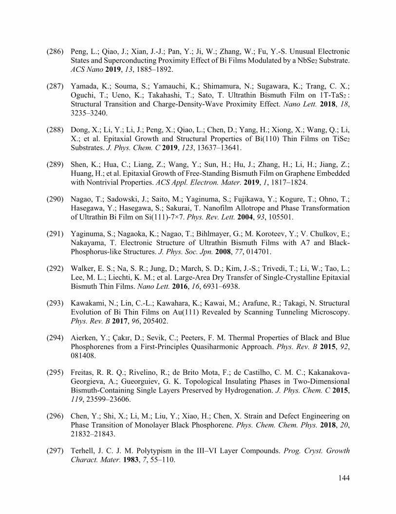
144
(286) Peng, L.; Qiao, J.; Xian, J.-J.; Pan, Y.; Ji, W.; Zhang, W.; Fu, Y.-S. Unusual Electronic
States and Superconducting Proximity Effect of Bi Films Modulated by a NbSe2 Substrate.
ACS Nano 2019, 13, 1885–1892.
(287) Yamada, K.; Souma, S.; Yamauchi, K.; Shimamura, N.; Sugawara, K.; Trang, C. X.;
Oguchi, T.; Ueno, K.; Takahashi, T.; Sato, T. Ultrathin Bismuth Film on 1T-TaS2 :
Structural Transition and Charge-Density-Wave Proximity Effect. Nano Lett. 2018, 18,
3235–3240.
(288) Dong, X.; Li, Y.; Li, J.; Peng, X.; Qiao, L.; Chen, D.; Yang, H.; Xiong, X.; Wang, Q.; Li,
X.; et al. Epitaxial Growth and Structural Properties of Bi(110) Thin Films on TiSe2
Substrates. J. Phys. Chem. C 2019, 123, 13637–13641.
(289) Shen, K.; Hua, C.; Liang, Z.; Wang, Y.; Sun, H.; Hu, J.; Zhang, H.; Li, H.; Jiang, Z.;
Huang, H.; et al. Epitaxial Growth of Free-Standing Bismuth Film on Graphene Embedded
with Nontrivial Properties. ACS Appl. Electron. Mater. 2019, 1, 1817–1824.
(290) Nagao, T.; Sadowski, J.; Saito, M.; Yaginuma, S.; Fujikawa, Y.; Kogure, T.; Ohno, T.;
Hasegawa, Y.; Hasegawa, S.; Sakurai, T. Nanofilm Allotrope and Phase Transformation
of Ultrathin Bi Film on Si(111)-7×7. Phys. Rev. Lett. 2004, 93, 105501.
(291) Yaginuma, S.; Nagaoka, K.; Nagao, T.; Bihlmayer, G.; M. Koroteev, Y.; V. Chulkov, E.;
Nakayama, T. Electronic Structure of Ultrathin Bismuth Films with A7 and Black-
Phosphorus-like Structures. J. Phys. Soc. Jpn. 2008, 77, 014701.
(292) Walker, E. S.; Na, S. R.; Jung, D.; March, S. D.; Kim, J.-S.; Trivedi, T.; Li, W.; Tao, L.;
Lee, M. L.; Liechti, K. M.; et al. Large-Area Dry Transfer of Single-Crystalline Epitaxial
Bismuth Thin Films. Nano Lett. 2016, 16, 6931–6938.
(293) Kawakami, N.; Lin, C.-L.; Kawahara, K.; Kawai, M.; Arafune, R.; Takagi, N. Structural
Evolution of Bi Thin Films on Au(111) Revealed by Scanning Tunneling Microscopy.
Phys. Rev. B 2017, 96, 205402.
(294) Aierken, Y.; Çakır, D.; Sevik, C.; Peeters, F. M. Thermal Properties of Black and Blue
Phosphorenes from a First-Principles Quasiharmonic Approach. Phys. Rev. B 2015, 92,
081408.
(295) Freitas, R. R. Q.; Rivelino, R.; de Brito Mota, F.; de Castilho, C. M. C.; Kakanakova-
Georgieva, A.; Gueorguiev, G. K. Topological Insulating Phases in Two-Dimensional
Bismuth-Containing Single Layers Preserved by Hydrogenation. J. Phys. Chem. C 2015,
119, 23599–23606.
(296) Chen, Y.; Shi, X.; Li, M.; Liu, Y.; Xiao, H.; Chen, X. Strain and Defect Engineering on
Phase Transition of Monolayer Black Phosphorene. Phys. Chem. Chem. Phys. 2018, 20,
21832–21843.
(297) Terhell, J. C. J. M. Polytypism in the III–VI Layer Compounds. Prog. Cryst. Growth
Charact. Mater. 1983, 7, 55–110.
145
(298) Diehl, R.; Nitsche, R. Vapour Growth of Three In2S3 Modifications by Iodine Transport.
J. Cryst. Growth 1975, 28, 306–310.
(299) Han, G.; Chen, Z.-G.; Sun, C.; Yang, L.; Cheng, L.; Li, Z.; Lu, W.; Gibbs, Z. M.; Snyder,
G. J.; Jack, K.; et al. A New Crystal: Layer-Structured Rhombohedral In3Se4.
CrystEngComm 2014, 16, 393–398.
(300) Hogg, J. H. C.; Sutherland, H. H.; Williams, D. J. The Crystal Structure of Tetraindium
Triselenide. Acta Crystallogr. B Struct. Crystallogr. Cryst. Chem. 1973, 29, 1590–1593.
(301) Hogg, J. H. C.; Sutherland, H. H. Indium Telluride. Acta Cryst B 1976, 32, 2689–2690.
(302) Serebryanaya, N. R. The Crystal Structure of Pressure-Induced Phases of In2Te3 and
Ga2Te3. Powder Diffr. 1992, 7, 99–102.
(303) Wasala, M.; Sirikumara, H. I.; Raj Sapkota, Y.; Hofer, S.; Mazumdar, D.; Jayasekera, T.;
Talapatra, S. Recent Advances in Investigations of the Electronic and Optoelectronic
Properties of Group III, IV, and V Selenide Based Binary Layered Compounds. J. Mater.
Chem. C 2017, 5, 11214–11225.
(304) Yang, Z.; Hao, J. Recent Progress in 2D Layered III–VI Semiconductors and Their
Heterostructures for Optoelectronic Device Applications. Adv. Mater. Technol. 2019, 4,
1900108.
(305) Cai, H.; Gu, Y.; Lin, Y.-C.; Yu, Y.; Geohegan, D. B.; Xiao, K. Synthesis and Emerging
Properties of 2D Layered III–VI Metal Chalcogenides. Appl. Phys. Rev. 2019, 6, 041312.
(306) Kolesnikov, N. N.; Borisenko, E. B.; Borisenko, D. N.; Timonina, A. V. Structure and
Microstructure of GaTe Crystals Grown by High-Pressure Vertical Zone Melting. J. Cryst.
Growth 2013, 365, 59–63.
(307) Sánchez-Royo, J. F.; Pellicer-Porres, J.; Segura, A.; Muñoz-Sanjosé, V.; Tobías, G.;
Ordejón, P.; Canadell, E.; Huttel, Y. Angle-Resolved Photoemission Study and First-
Principles Calculation of the Electronic Structure of GaTe. Phys. Rev. B 2002, 65, 115201.
(308) Bastow, T. J.; Campbell, I. D.; Whitfield, H. J. A 69Ga, 115In NQR Study of Polytypes of
GaS, GaSe and InSe. Solid State Commun. 1981, 39, 307–311.
(309) Kou, L.; Du, A.; Ma, Y.; Liao, T.; Chen, C. Charging Assisted Structural Phase Transitions
in Monolayer InSe. Phys. Chem. Chem. Phys. 2017, 19, 22502–22508.
(310) Autere, A.; Jussila, H.; Dai, Y.; Wang, Y.; Lipsanen, H.; Sun, Z. Nonlinear Optics with 2D
Layered Materials. Adv. Mater. 2018, 30, 1705963.
(311) Cui, C.; Xue, F.; Hu, W.-J.; Li, L.-J. Two-Dimensional Materials with Piezoelectric and
Ferroelectric Functionalities. npj 2D Mater. Appl. 2018, 2, 18.

146
(312) Li, W.; Li, J. Piezoelectricity in Two-Dimensional Group-III Monochalcogenides. Nano
Res. 2015, 8, 3796–3802.
(313) Dai, M.; Wang, Z.; Wang, F.; Qiu, Y.; Zhang, J.; Xu, C.-Y.; Zhai, T.; Cao, W.; Fu, Y.; Jia,
D.; et al. Two-Dimensional van der Waals Materials with Aligned In-Plane Polarization
and Large Piezoelectric Effect for Self-Powered Piezoelectric Sensors. Nano Lett. 2019,
19, 5410–5416.
(314) Zhou, X.; Cheng, J.; Zhou, Y.; Cao, T.; Hong, H.; Liao, Z.; Wu, S.; Peng, H.; Liu, K.; Yu,
D. Strong Second-Harmonic Generation in Atomic Layered GaSe. J. Am. Chem. Soc. 2015,
137, 7994–7997.
(315) Leisgang, N.; Roch, J. G.; Froehlicher, G.; Hamer, M.; Terry, D.; Gorbachev, R.;
Warburton, R. J. Optical Second Harmonic Generation in Encapsulated Single-Layer InSe.
AIP Advances 2018, 8, 105120.
(316) Huang, W.; Gan, L.; Li, H.; Ma, Y.; Zhai, T. Phase-Engineered Growth of Ultrathin InSe
Flakes by Chemical Vapor Deposition for High-Efficiency Second Harmonic Generation.
Chem. Eur. J. 2018, 24, 15678–15684.
(317) Hao, Q.; Yi, H.; Su, H.; Wei, B.; Wang, Z.; Lao, Z.; Chai, Y.; Wang, Z.; Jin, C.; Dai, J.; et
al. Phase Identification and Strong Second Harmonic Generation in Pure ε-InSe and Its
Alloys. Nano Lett. 2019, 19, 2634–2640.
(318) Zhou, J.; Shi, J.; Zeng, Q.; Chen, Y.; Niu, L.; Liu, F.; Yu, T.; Suenaga, K.; Liu, X.; Lin, J.;
et al. InSe Monolayer: Synthesis, Structure and Ultra-High Second-Harmonic Generation.
2D Mater. 2018, 5, 025019.
(319) Attaccalite, C.; Palummo, M.; Cannuccia, E.; Grüning, M. Second-Harmonic Generation
in Single-Layer Monochalcogenides: A Response from First-Principles Real-Time
Simulations. Phys. Rev. Materials 2019, 3, 074003.
(320) Hu, L.; Huang, X.; Wei, D. Layer-Independent and Layer-Dependent Nonlinear Optical
Properties of Two-Dimensional GaX (X = S, Se, Te) Nanosheets. Phys. Chem. Chem.
Phys. 2017, 19, 11131–11141.
(321) Plucinski, L.; Johnson, R. L.; Kowalski, B. J.; Kopalko, K.; Orlowski, B. A.; Kovalyuk, Z.
D.; Lashkarev, G. V. Electronic Band Structure of GaSe(0001): Angle-Resolved
Photoemission and Ab Initio Theory. Phys. Rev. B 2003, 68, 125304.
(322) Gomes da Costa, P.; Dandrea, R. G.; Wallis, R. F.; Balkanski, M. First-Principles Study of
the Electronic Structure of γ-InSe and β-InSe. Phys. Rev. B 1993, 48, 14135–14141.
(323) Srour, J.; Badawi, M.; El Haj Hassan, F.; Postnikov, A. Comparative Study of Structural
and Electronic Properties of GaSe and InSe Polytypes. J. Chem. Phys. 2018, 149, 054106.
(324) Sun, Y.; Luo, S.; Zhao, X.-G.; Biswas, K.; Li, S.-L.; Zhang, L. InSe: A Two-Dimensional
Material with Strong Interlayer Coupling. Nanoscale 2018, 10, 7991–7998.

147
(325) Huang, S.; Tatsumi, Y.; Ling, X.; Guo, H.; Wang, Z.; Watson, G.; Puretzky, A. A.;
Geohegan, D. B.; Kong, J.; Li, J.; et al. In-Plane Optical Anisotropy of Layered Gallium
Telluride. ACS Nano 2016, 10, 8964–8972.
(326) Susoma, J.; Karvonen, L.; Säynätjoki, A.; Mehravar, S.; Norwood, R. A.; Peyghambarian,
N.; Kieu, K.; Lipsanen, H.; Riikonen, J. Second and Third Harmonic Generation in Few-
Layer Gallium Telluride Characterized by Multiphoton Microscopy. Appl. Phys. Lett.
2016, 108, 073103.
(327) Kosobutsky, A. V.; Sarkisov, S. Yu. Influence of Size Effects on the Electronic Structure
of Hexagonal Gallium Telluride. Phys. Solid State 2018, 60, 1686–1690.
(328) Han, G.; Chen, Z.-G.; Drennan, J.; Zou, J. Indium Selenides: Structural Characteristics,
Synthesis and Their Thermoelectric Performances. Small 2014, 10, 2747–2765.
(329) Küpers, M.; Konze, P. M.; Meledin, A.; Mayer, J.; Englert, U.; Wuttig, M.; Dronskowski,
R. Controlled Crystal Growth of Indium Selenide, In2Se3 , and the Crystal Structures of α-
In2Se3. Inorg. Chem. 2018, 57, 11775–11781.
(330) Liu, L.; Dong, J.; Huang, J.; Nie, A.; Zhai, K.; Xiang, J.; Wang, B.; Wen, F.; Mu, C.; Zhao,
Z.; et al. Atomically Resolving Polymorphs and Crystal Structures of In2Se3. Chem. Mater.
2019, 31, 10143–10149.
(331) Li, W.; Sabino, F. P.; Crasto de Lima, F.; Wang, T.; Miwa, R. H.; Janotti, A. Large
Disparity between Optical and Fundamental Band Gaps in Layered In2Se3. Phys. Rev. B
2018, 98, 165134.
(332) Zheng, C.; Yu, L.; Zhu, L.; Collins, J. L.; Kim, D.; Lou, Y.; Xu, C.; Li, M.; Wei, Z.; Zhang,
Y.; et al. Room Temperature In-Plane Ferroelectricity in van der Waals In2Se3. Science
Advances 2018, 4, eaar7720.
(333) Collins, J. L.; Wang, C.; Tadich, A.; Yin, Y.; Zheng, C.; Hellerstedt, J.; Grubisić-Čabo,
A.; Tang, S.; Mo, S.-K.; Riley, J.; et al. Electronic Band Structure of In-Plane Ferroelectric
van der Waals Β′-In2Se3. ACS Appl. Electron. Mater. 2020, 2, 213–219.
(334) van Landuyt, J.; van Tendeloo, G.; Amelinckx, S. Phase Transitions in In2Se3 as Studied
by Electron Microscopy and Electron Diffraction. Phys. Stat. Sol. A 1975, 30, 299–314.
(335) Zhang, F.; Wang, Z.; Dong, J.; Nie, A.; Xiang, J.; Zhu, W.; Liu, Z.; Tao, C. Atomic-Scale
Observation of Reversible Thermally Driven Phase Transformation in 2D In2Se3. ACS
Nano 2019, 13, 8004–8011.
(336) Dong, J.; Liu, L.; Nie, A.; Xiang, J.; Zhai, K.; Wang, B.; Wen, F.; Mu, C.; Chen, Y.; Zhao,
Z.; et al. Influence of van der Waals Epitaxy on Phase Transformation Behaviors in 2D
Heterostructure. Appl. Phys. Lett. 2020, 116, 021602.
148
(337) Liu, J.; Pantelides, S. T. Pyroelectric Response and Temperature-Induced α - β Phase
Transitions in α-In2Se3 and Other α-III2VI3 (III = Al, Ga, In; VI = S, Se) Monolayers. 2D
Mater. 2019, 6, 025001.
(338) Ding, W.; Zhu, J.; Wang, Z.; Gao, Y.; Xiao, D.; Gu, Y.; Zhang, Z.; Zhu, W. Prediction of
Intrinsic Two-Dimensional Ferroelectrics in In2Se3 and Other III2-VI3 van der Waals
Materials. Nat Commun. 2017, 8, 14956.
(339) Xiao, J.; Zhu, H.; Wang, Y.; Feng, W.; Yunxia; Dasgupta, A.; Han, Y.; Wang, Y.; Muller,
D. A.; Martin, L. W.; et al. Intrinsic Two-Dimensional Ferroelectricity with Dipole
Locking. Phys. Rev. Lett. 2018, 120, 227601.
(340) Xue, F.; Hu, W.; Lee, K.; Lu, L.; Zhang, J.; Tang, H.; Han, A.; Hsu, W.; Tu, S.; Chang,
W.; et al. Room‐Temperature Ferroelectricity in Hexagonally Layered Α‐In2Se3
Nanoflakes down to the Monolayer Limit. Adv. Funct. Mater. 2018, 28, 1803738.
(341) Cui, C.; Hu, W.-J.; Yan, X.; Addiego, C.; Gao, W.; Wang, Y.; Wang, Z.; Li, L.; Cheng,
Y.; Li, P.; et al. Intercorrelated In-Plane and Out-of-Plane Ferroelectricity in Ultrathin
Two-Dimensional Layered Semiconductor In2Se3. Nano Lett. 2018, 18, 1253–1258.
(342) Zhou, Y.; Wu, D.; Zhu, Y.; Cho, Y.; He, Q.; Yang, X.; Herrera, K.; Chu, Z.; Han, Y.;
Downer, M. C.; et al. Out-of-Plane Piezoelectricity and Ferroelectricity in Layered α-
In2Se3 Nanoflakes. Nano Lett. 2017, 17, 5508–5513.
(343) Xue, F.; Zhang, J.; Hu, W.; Hsu, W.-T.; Han, A.; Leung, S.-F.; Huang, J.-K.; Wan, Y.; Liu,
S.; Zhang, J.; et al. Multidirection Piezoelectricity in Mono- and Multilayered Hexagonal
α-In2Se3. ACS Nano 2018, 12, 4976–4983.
(344) Tao, X.; Gu, Y. Crystalline–Crystalline Phase Transformation in Two-Dimensional In2Se3
Thin Layers. Nano Lett. 2013, 13, 3501–3505.
(345) Feng, W.; Gao, F.; Hu, Y.; Dai, M.; Liu, H.; Wang, L.; Hu, P. Phase-Engineering-Driven
Enhanced Electronic and Optoelectronic Performance of Multilayer In2Se3 Nanosheets.
ACS Appl. Mater. Interfaces 2018, 10, 27584–27588.
(346) Huang, L.; Chen, Z.; Li, J. Effects of Strain on the Band Gap and Effective Mass in Two-
Dimensional Monolayer GaX (X = S, Se, Te). RSC Adv. 2015, 5, 5788–5794.
(347) Ho, C. H.; Lin, S. L. Optical Properties of the Interband Transitions of Layered Gallium
Sulfide. J. Appl. Phys. 2006, 100, 083508.
(348) Demirci, S.; Avazlı, N.; Durgun, E.; Cahangirov, S. Structural and Electronic Properties
of Monolayer Group III Monochalcogenides. Phys. Rev. B 2017, 95, 115409.
(349) Jung, C. S.; Shojaei, F.; Park, K.; Oh, J. Y.; Im, H. S.; Jang, D. M.; Park, J.; Kang, H. S.
Red-to-Ultraviolet Emission Tuning of Two-Dimensional Gallium Sulfide/Selenide. ACS
Nano 2015, 9, 9585–9593.

149
(350) Ma, Y.; Dai, Y.; Guo, M.; Yu, L.; Huang, B. Tunable Electronic and Dielectric Behavior
of GaS and GaSe Monolayers. Phys. Chem. Chem. Phys. 2013, 15, 7098.
(351) Aulich, E.; Brebner, J. L.; Mooser, E. Indirect Energy Gap in GaSe and GaS. Phys. Stat.
Sol. B 1969, 31, 129–131.
(352) Kuhn, A.; Chevy, A.; Chevalier, R. Crystal Structure and Interatomic Distances in GaSe.
Phys. Stat. Sol. A 1975, 31, 469–475.
(353) Shenoy, U. S.; Gupta, U.; Narang, D. S.; Late, D. J.; Waghmare, U. V.; Rao, C. N. R.
Electronic Structure and Properties of Layered Gallium Telluride. Chem. Phys. Lett. 2016,
651, 148–154.
(354) Bose, D. N.; Pal, S. Photoconductivity, Low-Temperature Conductivity, and
Magnetoresistance Studies on the Layered Semiconductor GaTe. Phys. Rev. B 2001, 63,
235321.
(355) Borisenko, E.; Borisenko, D.; Timonina, A.; Kolesnikov, N. Nonvariant Polymorphic
Transition from Hexagonal to Monoclinic Lattice in GaTe Single Crystal. J. Cryst. Growth
2020, 535, 125548.
(356) Debbichi, L.; Eriksson, O.; Lebègue, S. Two-Dimensional Indium Selenides Compounds:
An Ab Initio Study. J. Phys. Chem. Lett. 2015, 6, 3098–3103.
(357) De Blasi, C.; Micocci, G.; Mongelli, S.; Tepore, A. Large InSe Single Crystals Grown
from Stoichiometric and Non-Stoichiometric Melts. J. Cryst. Growth 1982, 57, 482–486.
(358) Mudd, G. W.; Svatek, S. A.; Ren, T.; Patanè, A.; Makarovsky, O.; Eaves, L.; Beton, P. H.;
Kovalyuk, Z. D.; Lashkarev, G. V.; Kudrynskyi, Z. R.; et al. Tuning the Bandgap of
Exfoliated InSe Nanosheets by Quantum Confinement. Adv. Mater. 2013, 25, 5714–5718.
(359) Zhou, J.; Zeng, Q.; Lv, D.; Sun, L.; Niu, L.; Fu, W.; Liu, F.; Shen, Z.; Jin, C.; Liu, Z.
Controlled Synthesis of High-Quality Monolayered α-In2Se3 via Physical Vapor
Deposition. Nano Lett. 2015, 15, 6400–6405.
(360) Julien, C.; Chevy, A.; Siapkas, D. Optical Properties of In2Se3 Phases. Phys. Stat. Sol. A
1990, 118, 553–559.
(361) Almeida, G.; Dogan, S.; Bertoni, G.; Giannini, C.; Gaspari, R.; Perissinotto, S.; Krahne,
R.; Ghosh, S.; Manna, L. Colloidal Monolayer β-In2Se3 Nanosheets with High
Photoresponsivity. J. Am. Chem. Soc. 2017, 139, 3005–3011.
(362) Lutz, H. D.; Fischer, M.; Baldus, H.-P.; Blachnik, R. Zur polymorphie des In2Se3. J. Less
Common Met. 1988, 143, 83–92.
(363) Balakrishnan, N.; Steer, E. D.; Smith, E. F.; Kudrynskyi, Z. R.; Kovalyuk, Z. D.; Eaves,
L.; Patanè, A.; Beton, P. H. Epitaxial Growth of γ-InSe and α, β, and γ-In2Se3on ε-GaSe.
2D Materials 2018, 5, 035026.
150
(364) Hu, Y.; Feng, W.; Dai, M.; Yang, H.; Chen, X.; Liu, G.; Zhang, S.; Hu, P. Temperature-
Dependent Growth of Few Layer β -InSe and α -In2Se3 Single Crystals for Optoelectronic
Device. Semicond. Sci. Technol. 2018, 33, 125002.
(365) Lee, C. H.; Krishnamoorthy, S.; O’Hara, D. J.; Brenner, M. R.; Johnson, J. M.; Jamison,
J. S.; Myers, R. C.; Kawakami, R. K.; Hwang, J.; Rajan, S. Molecular Beam Epitaxy of
2D-Layered Gallium Selenide on GaN Substrates. J. Appl. Phys. 2017, 121, 094302.
(366) Longuinhos, R.; Ribeiro-Soares, J. Ultra-Weak Interlayer Coupling in Two-Dimensional
Gallium Selenide. Phys. Chem. Chem. Phys. 2016, 18, 25401–25408.
(367) Gillan, E. G.; Barron, A. R. Chemical Vapor Deposition of Hexagonal Gallium Selenide
and Telluride Films from Cubane Precursors: Understanding the Envelope of Molecular
Control. Chem. Mater. 1997, 9, 3037–3048.
(368) Yu, Y.; Ran, M.; Zhou, S.; Wang, R.; Zhou, F.; Li, H.; Gan, L.; Zhu, M.; Zhai, T. Phase‐
Engineered Synthesis of Ultrathin Hexagonal and Monoclinic GaTe Flakes and Phase
Transition Study. Adv. Funct. Mater. 2019, 29, 1901012.
(369) Li, J.-B.; Record, M.-C.; Tedenac, J.-C. A Thermodynamic Assessment of the In–Se
System. MEKU 2003, 94, 381–389.
(370) Lin, M.; Wu, D.; Zhou, Y.; Huang, W.; Jiang, W.; Zheng, W.; Zhao, S.; Jin, C.; Guo, Y.;
Peng, H.; et al. Controlled Growth of Atomically Thin In2Se3 Flakes by van der Waals
Epitaxy. J. Am. Chem. Soc. 2013, 135, 13274–13277.
(371) Zhang, X.; Lee, S.; Bansal, A.; Zhang, F.; Terrones, M.; Jackson, T. N.; Redwing, J. M.
Epitaxial Growth of Few-Layer β-In2Se3 Thin Films by Metalorganic Chemical Vapor
Deposition. J. Cryst. Growth 2020, 533, 125471.
(372) Bae, C. J.; McMahon, J.; Detz, H.; Strasser, G.; Park, J.; Einarsson, E.; Eason, D. B.
Influence of Thickness on Crystallinity in Wafer-Scale GaTe Nanolayers Grown by
Molecular Beam Epitaxy. AIP Advances 2017, 7, 035113.
(373) Yonezawa, T.; Murakami, T.; Higashimine, K.; Fleurence, A.; Oshima, Y.; Yamada-
Takamura, Y. Atomistic Study of GaSe/Ge(111) Interface Formed through van der Waals
Epitaxy. Surf. Interface Anal. 2019, 51, 95–99.
(374) Diep, N. Q.; Liu, C.-W.; Wu, S.-K.; Chou, W.-C.; Huynh, S. H.; Chang, E. Y. Screw-
Dislocation-Driven Growth Mode in Two Dimensional GaSe on GaAs(001) Substrates
Grown by Molecular Beam Epitaxy. Sci. Rep. 2019, 9, 17781.
(375) Feng, W.; Qin, F.; Yu, M.; Gao, F.; Dai, M.; Hu, Y.; Wang, L.; Hou, J.; Li, B.; Hu, P.
Synthesis of Superlattice InSe Nanosheets with Enhanced Electronic and Optoelectronic
Performance. ACS Appl. Mater. Interfaces 2019, 11, 18511–18516.
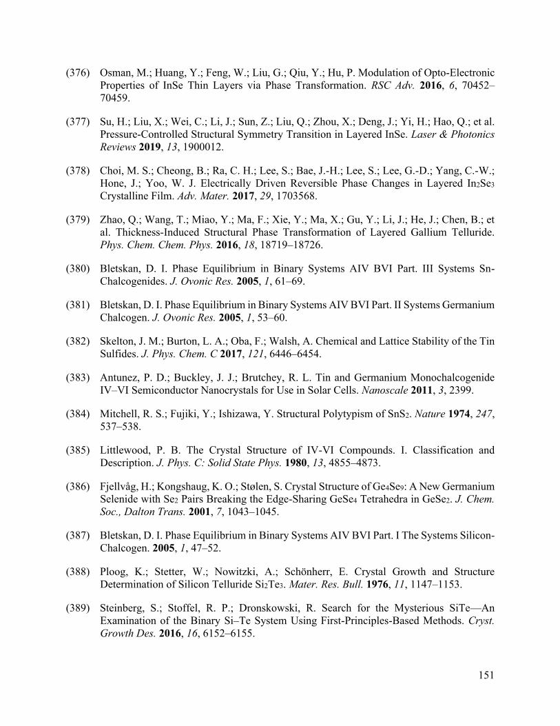
151
(376) Osman, M.; Huang, Y.; Feng, W.; Liu, G.; Qiu, Y.; Hu, P. Modulation of Opto-Electronic
Properties of InSe Thin Layers via Phase Transformation. RSC Adv. 2016, 6, 70452–
70459.
(377) Su, H.; Liu, X.; Wei, C.; Li, J.; Sun, Z.; Liu, Q.; Zhou, X.; Deng, J.; Yi, H.; Hao, Q.; et al.
Pressure‐Controlled Structural Symmetry Transition in Layered InSe. Laser & Photonics
Reviews 2019, 13, 1900012.
(378) Choi, M. S.; Cheong, B.; Ra, C. H.; Lee, S.; Bae, J.-H.; Lee, S.; Lee, G.-D.; Yang, C.-W.;
Hone, J.; Yoo, W. J. Electrically Driven Reversible Phase Changes in Layered In2Se3
Crystalline Film. Adv. Mater. 2017, 29, 1703568.
(379) Zhao, Q.; Wang, T.; Miao, Y.; Ma, F.; Xie, Y.; Ma, X.; Gu, Y.; Li, J.; He, J.; Chen, B.; et
al. Thickness-Induced Structural Phase Transformation of Layered Gallium Telluride.
Phys. Chem. Chem. Phys. 2016, 18, 18719–18726.
(380) Bletskan, D. I. Phase Equilibrium in Binary Systems AIV BVI Part. III Systems Sn-
Chalcogenides. J. Ovonic Res. 2005, 1, 61–69.
(381) Bletskan, D. I. Phase Equilibrium in Binary Systems AIV BVI Part. II Systems Germanium
Chalcogen. J. Ovonic Res. 2005, 1, 53–60.
(382) Skelton, J. M.; Burton, L. A.; Oba, F.; Walsh, A. Chemical and Lattice Stability of the Tin
Sulfides. J. Phys. Chem. C 2017, 121, 6446–6454.
(383) Antunez, P. D.; Buckley, J. J.; Brutchey, R. L. Tin and Germanium Monochalcogenide
IV–VI Semiconductor Nanocrystals for Use in Solar Cells. Nanoscale 2011, 3, 2399.
(384) Mitchell, R. S.; Fujiki, Y.; Ishizawa, Y. Structural Polytypism of SnS2. Nature 1974, 247,
537–538.
(385) Littlewood, P. B. The Crystal Structure of IV-VI Compounds. I. Classification and
Description. J. Phys. C: Solid State Phys. 1980, 13, 4855–4873.
(386) Fjellvåg, H.; Kongshaug, K. O.; Stølen, S. Crystal Structure of Ge4Se9: A New Germanium
Selenide with Se2 Pairs Breaking the Edge-Sharing GeSe4 Tetrahedra in GeSe2. J. Chem.
Soc., Dalton Trans. 2001, 7, 1043–1045.
(387) Bletskan, D. I. Phase Equilibrium in Binary Systems AIV BVI Part. I The Systems Silicon-
Chalcogen. 2005, 1, 47–52.
(388) Ploog, K.; Stetter, W.; Nowitzki, A.; Schönherr, E. Crystal Growth and Structure
Determination of Silicon Telluride Si2Te3. Mater. Res. Bull. 1976, 11, 1147–1153.
(389) Steinberg, S.; Stoffel, R. P.; Dronskowski, R. Search for the Mysterious SiTe—An
Examination of the Binary Si–Te System Using First-Principles-Based Methods. Cryst.
Growth Des. 2016, 16, 6152–6155.
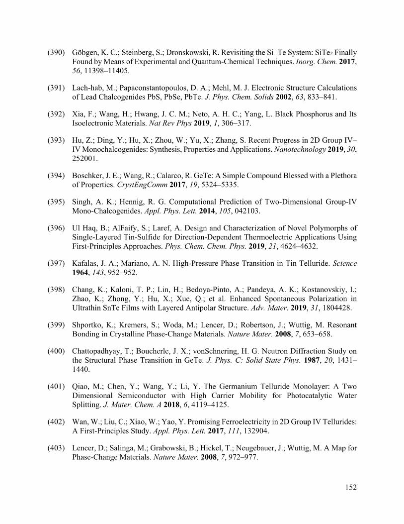
152
(390) Göbgen, K. C.; Steinberg, S.; Dronskowski, R. Revisiting the Si–Te System: SiTe2 Finally
Found by Means of Experimental and Quantum-Chemical Techniques. Inorg. Chem. 2017,
56, 11398–11405.
(391) Lach-hab, M.; Papaconstantopoulos, D. A.; Mehl, M. J. Electronic Structure Calculations
of Lead Chalcogenides PbS, PbSe, PbTe. J. Phys. Chem. Solids 2002, 63, 833–841.
(392) Xia, F.; Wang, H.; Hwang, J. C. M.; Neto, A. H. C.; Yang, L. Black Phosphorus and Its
Isoelectronic Materials. Nat Rev Phys 2019, 1, 306–317.
(393) Hu, Z.; Ding, Y.; Hu, X.; Zhou, W.; Yu, X.; Zhang, S. Recent Progress in 2D Group IV–
IV Monochalcogenides: Synthesis, Properties and Applications. Nanotechnology 2019, 30,
252001.
(394) Boschker, J. E.; Wang, R.; Calarco, R. GeTe: A Simple Compound Blessed with a Plethora
of Properties. CrystEngComm 2017, 19, 5324–5335.
(395) Singh, A. K.; Hennig, R. G. Computational Prediction of Two-Dimensional Group-IV
Mono-Chalcogenides. Appl. Phys. Lett. 2014, 105, 042103.
(396) Ul Haq, B.; AlFaify, S.; Laref, A. Design and Characterization of Novel Polymorphs of
Single-Layered Tin-Sulfide for Direction-Dependent Thermoelectric Applications Using
First-Principles Approaches. Phys. Chem. Chem. Phys. 2019, 21, 4624–4632.
(397) Kafalas, J. A.; Mariano, A. N. High-Pressure Phase Transition in Tin Telluride. Science
1964, 143, 952–952.
(398) Chang, K.; Kaloni, T. P.; Lin, H.; Bedoya‐Pinto, A.; Pandeya, A. K.; Kostanovskiy, I.;
Zhao, K.; Zhong, Y.; Hu, X.; Xue, Q.; et al. Enhanced Spontaneous Polarization in
Ultrathin SnTe Films with Layered Antipolar Structure. Adv. Mater. 2019, 31, 1804428.
(399) Shportko, K.; Kremers, S.; Woda, M.; Lencer, D.; Robertson, J.; Wuttig, M. Resonant
Bonding in Crystalline Phase-Change Materials. Nature Mater. 2008, 7, 653–658.
(400) Chattopadhyay, T.; Boucherle, J. X.; vonSchnering, H. G. Neutron Diffraction Study on
the Structural Phase Transition in GeTe. J. Phys. C: Solid State Phys. 1987, 20, 1431–
1440.
(401) Qiao, M.; Chen, Y.; Wang, Y.; Li, Y. The Germanium Telluride Monolayer: A Two
Dimensional Semiconductor with High Carrier Mobility for Photocatalytic Water
Splitting. J. Mater. Chem. A 2018, 6, 4119–4125.
(402) Wan, W.; Liu, C.; Xiao, W.; Yao, Y. Promising Ferroelectricity in 2D Group IV Tellurides:
A First-Principles Study. Appl. Phys. Lett. 2017, 111, 132904.
(403) Lencer, D.; Salinga, M.; Grabowski, B.; Hickel, T.; Neugebauer, J.; Wuttig, M. A Map for
Phase-Change Materials. Nature Mater. 2008, 7, 972–977.

153
(404) Iizumi, M.; Hamaguchi, Y.; F. Komatsubara, K.; Kato, Y. Phase Transition in SnTe with
Low Carrier Concentration. J. Phys. Soc. Jpn. 1975, 38, 443–449.
(405) Zhu, Z.; Guan, J.; Liu, D.; Tománek, D. Designing Isoelectronic Counterparts to Layered
Group V Semiconductors. ACS Nano 2015, 9, 8284–8290.
(406) Hu, T.; Dong, J. Two New Phases of Monolayer Group-IV Monochalcogenides and Their
Piezoelectric Properties. Phys. Chem. Chem. Phys. 2016, 18, 32514–32520.
(407) Alonso-Lanza, T.; Ayuela, A.; Aguilera-Granja, F. An Array of Layers in Silicon Sulfides:
Chainlike and Monolayer. Phys. Rev. B 2016, 94, 245441.
(408) Yang, J.-H.; Zhang, Y.; Yin, W.-J.; Gong, X. G.; Yakobson, B. I.; Wei, S.-H. Two-
Dimensional SiS Layers with Promising Electronic and Optoelectronic Properties:
Theoretical Prediction. Nano Lett. 2016, 16, 1110–1117.
(409) Hu, Z.-Y.; Li, K.-Y.; Lu, Y.; Huang, Y.; Shao, X.-H. High Thermoelectric Performances
of Monolayer SnSe Allotropes. Nanoscale 2017, 9, 16093–16100.
(410) Wu, M.; Wei, S.-H.; Huang, L. Origin of Polymorphism of the Two-Dimensional Group-
IV Monochalcogenides. Phys. Rev. B 2017, 96, 205411.
(411) Luo, N.; Wang, C.; Jiang, Z.; Xu, Y.; Zou, X.; Duan, W. Saddle-Point Excitons and Their
Extraordinary Light Absorption in 2D β-Phase Group-IV Monochalcogenides. Adv. Funct.
Mater. 2018, 28, 1804581.
(412) Dong, B.; Wang, Z.; Hung, N. T.; Oganov, A. R.; Yang, T.; Saito, R.; Zhang, Z. New Two-
Dimensional Phase of Tin Chalcogenides: Candidates for High-Performance
Thermoelectric Materials. Phys. Rev. Materials 2019, 3, 013405.
(413) Li, Z.-Y.; Liu, M.-Y.; Huang, Y.; Chen, Q.-Y.; Cao, C.; He, Y. Tuning the Electronic
Properties of Bilayer Group-IV Monochalcogenides by Stacking Order, Strain and an
Electric Field: A Computational Study. Phys. Chem. Chem. Phys. 2018, 20, 214–220.
(414) Mao, Y.; Xu, C.; Yuan, J.; Zhao, H. Effect of Stacking Order and In-Plane Strain on the
Electronic Properties of Bilayer GeSe. Phys. Chem. Chem. Phys. 2018, 20, 6929–6935.
(415) Yang, J.-H.; Gong, X.-G. Stacking Induced Indirect-to-Direct Bandgap Transition in
Layered Group-IV Monochalcogenides for Ideal Optoelectronics. J. Mater. Chem. C 2019,
7, 11858–11867.
(416) Zhang, J.; Lang, X. Y.; Jiang, Q. Electronic and Optical Properties of Bilayer SnS with
Different Stacking Orders: A First Principles Study. J. Appl. Phys. 2018, 124, 235101.
(417) Gomes, L. C.; Carvalho, A. Phosphorene Analogues: Isoelectronic Two-Dimensional
Group-IV Monochalcogenides with Orthorhombic Structure. Phys. Rev. B 2015, 92,
085406.
154
(418) Huang, L.; Wu, F.; Li, J. Structural Anisotropy Results in Strain-Tunable Electronic and
Optical Properties in Monolayer GeX and SnX (X = S, Se, Te). J. Chem. Phys. 2016, 144,
114708.
(419) Qin, G.; Qin, Z.; Fang, W.-Z.; Zhang, L.-C.; Yue, S.-Y.; Yan, Q.-B.; Hu, M.; Su, G.
Diverse Anisotropy of Phonon Transport in Two-Dimensional Group IV–VI Compounds:
A Comparative Study. Nanoscale 2016, 8, 11306–11319.
(420) Li, Z.; Yang, Y.; Wang, X.; Shi, W.; Xue, D.-J.; Hu, J.-S. Three-Dimensional Optical
Anisotropy of Low-Symmetry Layered GeS. ACS Appl. Mater. Interfaces 2019, 11,
24247–24253.
(421) Tian, Z.; Guo, C.; Zhao, M.; Li, R.; Xue, J. Two-Dimensional SnS: A Phosphorene
Analogue with Strong In-Plane Electronic Anisotropy. ACS Nano 2017, 11, 2219–2226.
(422) Xu, X.; Song, Q.; Wang, H.; Li, P.; Zhang, K.; Wang, Y.; Yuan, K.; Yang, Z.; Ye, Y.; Dai,
L. In-Plane Anisotropies of Polarized Raman Response and Electrical Conductivity in
Layered Tin Selenide. ACS Appl. Mater. Interfaces 2017, 9, 12601–12607.
(423) Shi, G.; Kioupakis, E. Anisotropic Spin Transport and Strong Visible-Light Absorbance
in Few-Layer SnSe and GeSe. Nano Lett. 2015, 15, 6926–6931.
(424) Gomes, L. C.; Carvalho, A.; Castro Neto, A. H. Enhanced Piezoelectricity and Modified
Dielectric Screening of Two-Dimensional Group-IV Monochalcogenides. Phys. Rev. B
2015, 92, 214103.
(425) Guo, Y.; Zhou, S.; Bai, Y.; Zhao, J. Oxidation Resistance of Monolayer Group-IV
Monochalcogenides. ACS Appl. Mater. Interfaces 2017, 9, 12013–12020.
(426) Wang, H.; Qian, X. Two-Dimensional Multiferroics in Monolayer Group IV
Monochalcogenides. 2D Mater. 2017, 4, 015042.
(427) Tang, X.; Kou, L. Two-Dimensional Ferroics and Multiferroics: Platforms for New
Physics and Applications. J. Phys. Chem. Lett. 2019, 10, 6634–6649.
(428) Wang, H.; Qian, X. Giant Optical Second Harmonic Generation in Two-Dimensional
Multiferroics. Nano Lett. 2017, 17, 5027–5034.
(429) Chang, K.; Liu, J.; Lin, H.; Wang, N.; Zhao, K.; Zhang, A.; Jin, F.; Zhong, Y.; Hu, X.;
Duan, W.; et al. Discovery of Robust In-Plane Ferroelectricity in Atomic-Thick SnTe.
Science 2016, 353, 274–278.
(430) Bao, Y.; Song, P.; Liu, Y.; Chen, Z.; Zhu, M.; Abdelwahab, I.; Su, J.; Fu, W.; Chi, X.; Yu,
W.; et al. Gate-Tunable In-Plane Ferroelectricity in Few-Layer SnS. Nano Lett. 2019, 19,
5109–5117.
155
(431) Sutter, P.; Sutter, E. Growth Mechanisms of Anisotropic Layered Group IV Chalcogenides
on van der Waals Substrates for Energy Conversion Applications. ACS Appl. Nano Mater.
2018, 1, 3026–3034.
(432) Jiang, J.; Wong, C. P. Y.; Zou, J.; Li, S.; Wang, Q.; Chen, J.; Qi, D.; Wang, H.; Eda, G.;
Chua, D. H. C.; et al. Two-Step Fabrication of Single-Layer Rectangular SnSe Flakes. 2D
Mater. 2017, 4, 021026.
(433) Kolobov, A. V.; Kim, D. J.; Giussani, A.; Fons, P.; Tominaga, J.; Calarco, R.; Gruverman,
A. Ferroelectric Switching in Epitaxial GeTe Films. APL Materials 2014, 2, 066101.
(434) Polking, M. J.; Urban, J. J.; Milliron, D. J.; Zheng, H.; Chan, E.; Caldwell, M. A.; Raoux,
S.; Kisielowski, C. F.; Ager, J. W.; Ramesh, R.; et al. Size-Dependent Polar Ordering in
Colloidal GeTe Nanocrystals. Nano Lett. 2011, 11, 1147–1152.
(435) Lucovsky, G.; White, R. M. Effects of Resonance Bonding on the Properties of Crystalline
and Amorphous Semiconductors. Phys. Rev. B 1973, 8, 660–667.
(436) Kaloni, T. P.; Chang, K.; Miller, B. J.; Xue, Q.-K.; Chen, X.; Ji, S.-H.; Parkin, S. S. P.;
Barraza-Lopez, S. From an Atomic Layer to the Bulk: Low-Temperature Atomistic
Structure and Ferroelectric and Electronic Properties of SnTe Films. Phys. Rev. B 2019,
99, 134108.
(437) Tanaka, Y.; Ren, Z.; Sato, T.; Nakayama, K.; Souma, S.; Takahashi, T.; Segawa, K.; Ando,
Y. Experimental Realization of a Topological Crystalline Insulator in SnTe. Nature Phys
2012, 8, 800–803.
(438) Dittmar, G.; Schäfer, H. Die Kristallstruktur von H.T.-GeS2. Acta Crystallogr. B Struct.
Sci. 1975, 31, 2060–2064.
(439) Dittmar, G.; Schäfer, H. Die Kristallstruktur von Germaniumdiselenid. Acta Cryst. B 1976,
32, 2726–2728.
(440) Fuentes-Cabrera, M.; Wang, H.; Sankey, O. F. Phase Stability and Pressure-Induced
Semiconductor to Metal Transition in Crystalline GeSe2. J. Phys.: Condens. Matter 2002,
14, 9589–9600.
(441) Popović, Z. V.; Holtz, M.; Reimann, K.; Syassen, K. High-Pressure Raman Scattering and
Optical Absorption Study of β-GeS2. Phys. Stat. Sol. B 1996, 198, 533–537.
(442) Dittmar, W. G.; Schäfer, H. Die Kristallstruktur von L.T.-GeS2. Acta Crystallographica
Section B 1976, 32, 1188–1192.
(443) Yang, Y.; Liu, S.; Wang, X.; Li, Z.; Zhang, Y.; Zhang, G.; Xue, D.; Hu, J. Polarization‐
Sensitive Ultraviolet Photodetection of Anisotropic 2D GeS2. Adv. Funct. Mater. 2019, 29,
1900411.
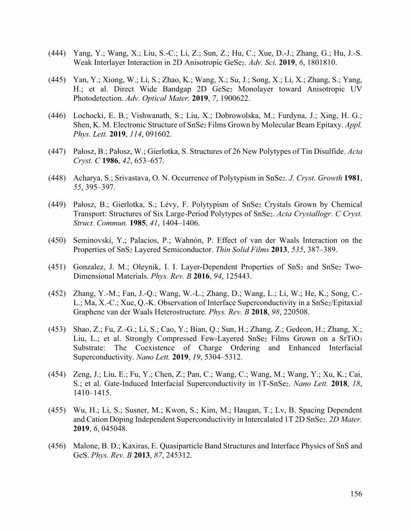
156
(444) Yang, Y.; Wang, X.; Liu, S.-C.; Li, Z.; Sun, Z.; Hu, C.; Xue, D.-J.; Zhang, G.; Hu, J.-S.
Weak Interlayer Interaction in 2D Anisotropic GeSe2. Adv. Sci. 2019, 6, 1801810.
(445) Yan, Y.; Xiong, W.; Li, S.; Zhao, K.; Wang, X.; Su, J.; Song, X.; Li, X.; Zhang, S.; Yang,
H.; et al. Direct Wide Bandgap 2D GeSe2 Monolayer toward Anisotropic UV
Photodetection. Adv. Optical Mater. 2019, 7, 1900622.
(446) Lochocki, E. B.; Vishwanath, S.; Liu, X.; Dobrowolska, M.; Furdyna, J.; Xing, H. G.;
Shen, K. M. Electronic Structure of SnSe2 Films Grown by Molecular Beam Epitaxy. Appl.
Phys. Lett. 2019, 114, 091602.
(447) Pałosz, B.; Pałosz, W.; Gierlotka, S. Structures of 26 New Polytypes of Tin Disulfide. Acta
Cryst. C 1986, 42, 653–657.
(448) Acharya, S.; Srivastava, O. N. Occurrence of Polytypism in SnSe2. J. Cryst. Growth 1981,
55, 395–397.
(449) Pałosz, B.; Gierlotka, S.; Lévy, F. Polytypism of SnSe2 Crystals Grown by Chemical
Transport: Structures of Six Large-Period Polytypes of SnSe2. Acta Crystallogr. C Cryst.
Struct. Commun. 1985, 41, 1404–1406.
(450) Seminovski, Y.; Palacios, P.; Wahnón, P. Effect of van der Waals Interaction on the
Properties of SnS2 Layered Semiconductor. Thin Solid Films 2013, 535, 387–389.
(451) Gonzalez, J. M.; Oleynik, I. I. Layer-Dependent Properties of SnS2 and SnSe2 Two-
Dimensional Materials. Phys. Rev. B 2016, 94, 125443.
(452) Zhang, Y.-M.; Fan, J.-Q.; Wang, W.-L.; Zhang, D.; Wang, L.; Li, W.; He, K.; Song, C.-
L.; Ma, X.-C.; Xue, Q.-K. Observation of Interface Superconductivity in a SnSe2/Epitaxial
Graphene van der Waals Heterostructure. Phys. Rev. B 2018, 98, 220508.
(453) Shao, Z.; Fu, Z.-G.; Li, S.; Cao, Y.; Bian, Q.; Sun, H.; Zhang, Z.; Gedeon, H.; Zhang, X.;
Liu, L.; et al. Strongly Compressed Few-Layered SnSe2 Films Grown on a SrTiO3
Substrate: The Coexistence of Charge Ordering and Enhanced Interfacial
Superconductivity. Nano Lett. 2019, 19, 5304–5312.
(454) Zeng, J.; Liu, E.; Fu, Y.; Chen, Z.; Pan, C.; Wang, C.; Wang, M.; Wang, Y.; Xu, K.; Cai,
S.; et al. Gate-Induced Interfacial Superconductivity in 1T-SnSe2. Nano Lett. 2018, 18,
1410–1415.
(455) Wu, H.; Li, S.; Susner, M.; Kwon, S.; Kim, M.; Haugan, T.; Lv, B. Spacing Dependent
and Cation Doping Independent Superconductivity in Intercalated 1T 2D SnSe2. 2D Mater.
2019, 6, 045048.
(456) Malone, B. D.; Kaxiras, E. Quasiparticle Band Structures and Interface Physics of SnS and
GeS. Phys. Rev. B 2013, 87, 245312.
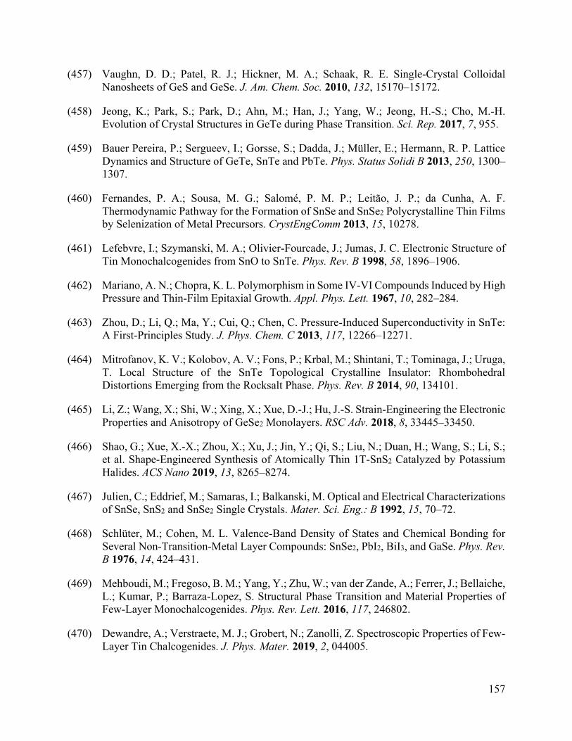
157
(457) Vaughn, D. D.; Patel, R. J.; Hickner, M. A.; Schaak, R. E. Single-Crystal Colloidal
Nanosheets of GeS and GeSe. J. Am. Chem. Soc. 2010, 132, 15170–15172.
(458) Jeong, K.; Park, S.; Park, D.; Ahn, M.; Han, J.; Yang, W.; Jeong, H.-S.; Cho, M.-H.
Evolution of Crystal Structures in GeTe during Phase Transition. Sci. Rep. 2017, 7, 955.
(459) Bauer Pereira, P.; Sergueev, I.; Gorsse, S.; Dadda, J.; Müller, E.; Hermann, R. P. Lattice
Dynamics and Structure of GeTe, SnTe and PbTe. Phys. Status Solidi B 2013, 250, 1300–
1307.
(460) Fernandes, P. A.; Sousa, M. G.; Salomé, P. M. P.; Leitão, J. P.; da Cunha, A. F.
Thermodynamic Pathway for the Formation of SnSe and SnSe2 Polycrystalline Thin Films
by Selenization of Metal Precursors. CrystEngComm 2013, 15, 10278.
(461) Lefebvre, I.; Szymanski, M. A.; Olivier-Fourcade, J.; Jumas, J. C. Electronic Structure of
Tin Monochalcogenides from SnO to SnTe. Phys. Rev. B 1998, 58, 1896–1906.
(462) Mariano, A. N.; Chopra, K. L. Polymorphism in Some IV-VI Compounds Induced by High
Pressure and Thin-Film Epitaxial Growth. Appl. Phys. Lett. 1967, 10, 282–284.
(463) Zhou, D.; Li, Q.; Ma, Y.; Cui, Q.; Chen, C. Pressure-Induced Superconductivity in SnTe:
A First-Principles Study. J. Phys. Chem. C 2013, 117, 12266–12271.
(464) Mitrofanov, K. V.; Kolobov, A. V.; Fons, P.; Krbal, M.; Shintani, T.; Tominaga, J.; Uruga,
T. Local Structure of the SnTe Topological Crystalline Insulator: Rhombohedral
Distortions Emerging from the Rocksalt Phase. Phys. Rev. B 2014, 90, 134101.
(465) Li, Z.; Wang, X.; Shi, W.; Xing, X.; Xue, D.-J.; Hu, J.-S. Strain-Engineering the Electronic
Properties and Anisotropy of GeSe2 Monolayers. RSC Adv. 2018, 8, 33445–33450.
(466) Shao, G.; Xue, X.-X.; Zhou, X.; Xu, J.; Jin, Y.; Qi, S.; Liu, N.; Duan, H.; Wang, S.; Li, S.;
et al. Shape-Engineered Synthesis of Atomically Thin 1T-SnS2 Catalyzed by Potassium
Halides. ACS Nano 2019, 13, 8265–8274.
(467) Julien, C.; Eddrief, M.; Samaras, I.; Balkanski, M. Optical and Electrical Characterizations
of SnSe, SnS2 and SnSe2 Single Crystals. Mater. Sci. Eng.: B 1992, 15, 70–72.
(468) Schlüter, M.; Cohen, M. L. Valence-Band Density of States and Chemical Bonding for
Several Non-Transition-Metal Layer Compounds: SnSe2, PbI2, BiI3, and GaSe. Phys. Rev.
B 1976, 14, 424–431.
(469) Mehboudi, M.; Fregoso, B. M.; Yang, Y.; Zhu, W.; van der Zande, A.; Ferrer, J.; Bellaiche,
L.; Kumar, P.; Barraza-Lopez, S. Structural Phase Transition and Material Properties of
Few-Layer Monochalcogenides. Phys. Rev. Lett. 2016, 117, 246802.
(470) Dewandre, A.; Verstraete, M. J.; Grobert, N.; Zanolli, Z. Spectroscopic Properties of Few-
Layer Tin Chalcogenides. J. Phys. Mater. 2019, 2, 044005.
158
(471) Poudel, S. P.; Villanova, J. W.; Barraza-Lopez, S. Group-IV Monochalcogenide
Monolayers: Two-Dimensional Ferroelectrics with Weak Intralayer Bonds and a
Phosphorenelike Monolayer Dissociation Energy. Phys. Rev. Materials 2019, 3, 124004.
(472) Mutlu, Z.; Wu, R. J.; Wickramaratne, D.; Shahrezaei, S.; Liu, C.; Temiz, S.; Patalano, A.;
Ozkan, M.; Lake, R. K.; Mkhoyan, K. A.; et al. Phase Engineering of 2D Tin Sulfides.
Small 2016, 12, 2998–3004.
(473) Huang, Y.; Xu, K.; Wang, Z.; Shifa, T. A.; Wang, Q.; Wang, F.; Jiang, C.; He, J. Designing
the Shape Evolution of SnSe2 Nanosheets and Their Optoelectronic Properties. Nanoscale
2015, 7, 17375–17380.
(474) Burton, L. A.; Colombara, D.; Abellon, R. D.; Grozema, F. C.; Peter, L. M.; Savenije, T.
J.; Dennler, G.; Walsh, A. Synthesis, Characterization, and Electronic Structure of Single-
Crystal SnS, Sn2S3, and SnS2. Chem. Mater. 2013, 25, 4908–4916.
(475) Li, M.; Zhu, Y.; Li, T.; Lin, Y.; Cai, H.; Li, S.; Ding, H.; Pan, N.; Wang, X. One-Step CVD
Fabrication and Optoelectronic Properties of SnS2/SnS Vertical Heterostructures. Inorg.
Chem. Front. 2018, 5, 1828–1835.
(476) Wang, Z.; Pang, F. A Facile Way to Control Phase of Tin Selenide Flakes by Chemical
Vapor Deposition. Chem. Phys. Lett. 2018, 702, 90–95.
(477) Zhang, H.; Balaji, Y.; Nalin Mehta, A.; Heyns, M.; Caymax, M.; Radu, I.; Vandervorst,
W.; Delabie, A. Formation Mechanism of 2D SnS2 and SnS by Chemical Vapor Deposition
Using SnCl4 and H2S. J. Mater. Chem. C 2018, 6, 6172–6178.
(478) Ahn, J.-H.; Lee, M.-J.; Heo, H.; Sung, J. H.; Kim, K.; Hwang, H.; Jo, M.-H. Deterministic
Two-Dimensional Polymorphism Growth of Hexagonal n-Type SnS2 and Orthorhombic
p-Type SnS Crystals. Nano Lett. 2015, 15, 3703–3708.
(479) Chang, K.; Parkin, S. S. P. The Growth and Phase Distribution of Ultrathin SnTe on
Graphene. APL Materials 2019, 7, 041102.
(480) Chen, H.; Keiser, C.; Du, S.; Gao, H.-J.; Sutter, P.; Sutter, E. Termination of Ge Surfaces
with Ultrathin GeS and GeS2 Layers via Solid-State Sulfurization. Phys. Chem. Chem.
Phys. 2017, 19, 32473–32480.
(481) Giussani, A.; Perumal, K.; Hanke, M.; Rodenbach, P.; Riechert, H.; Calarco, R. On the
Epitaxy of Germanium Telluride Thin Films on Silicon Substrates. Phys. Status Solidi B
2012, 249, 1939–1944.
(482) Wang, R.; Zhang, W.; Momand, J.; Ronneberger, I.; Boschker, J. E.; Mazzarello, R.; Kooi,
B. J.; Riechert, H.; Wuttig, M.; Calarco, R. Formation of Resonant Bonding during Growth
of Ultrathin GeTe Films. NPG Asia Mater. 2017, 9, e396.

159
(483) Wang, R.; Campi, D.; Bernasconi, M.; Momand, J.; Kooi, B. J.; Verheijen, M. A.; Wuttig,
M.; Calarco, R. Ordered Peierls Distortion Prevented at Growth Onset of GeTe Ultra-Thin
Films. Sci. Rep. 2016, 6, 32895.
(484) Hilmi, I.; Lotnyk, A.; Gerlach, J. W.; Schumacher, P.; Rauschenbach, B. Influence of
Substrate Dimensionality on the Growth Mode of Epitaxial 3D-Bonded GeTe Thin Films:
From 3D to 2D Growth. Materials & Design 2019, 168, 107657.
(485) Simpson, R. E.; Fons, P.; Kolobov, A. V.; Krbal, M.; Tominaga, J. Enhanced
Crystallization of GeTe from an Sb2Te3 Template. Appl. Phys. Lett. 2012, 100, 021911.
(486) Tsunetomo, K.; Sugishima, T.; Imura, T.; Osaka, Y. Stability of Metastable GeTe2 in Thin
Films. J. Non-Cryst. Solids 1987, 95–96, 509–516.
(487) Wang, J.; Ronneberger, I.; Zhou, L.; Lu, L.; Deringer, V. L.; Zhang, B.; Tian, L.; Du, H.;
Jia, C.; Qian, X.; et al. Unconventional Two-Dimensional Germanium Dichalcogenides.
Nanoscale 2018, 10, 7363–7368.
(488) Zhou, T.; Pang, W. K.; Zhang, C.; Yang, J.; Chen, Z.; Liu, H. K.; Guo, Z. Enhanced
Sodium-Ion Battery Performance by Structural Phase Transition from Two-Dimensional
Hexagonal-SnS2 to Orthorhombic-SnS. ACS Nano 2014, 8, 8323–8333.
(489) Tian, Z.; Zhao, M.; Xue, X.; Xia, W.; Guo, C.; Guo, Y.; Feng, Y.; Xue, J. Lateral
Heterostructures Formed by Thermally Converting N-Type SnSe2 to p-Type SnSe. ACS
Appl. Mater. Interfaces 2018, 10, 12831–12838.
(490) Sutter, P.; Ibragimova, R.; Komsa, H.-P.; Parkinson, B. A.; Sutter, E. Self-Organized
Twist-Heterostructures via Aligned van der Waals Epitaxy and Solid-State
Transformations. Nat. Commun. 2019, 10, 5528.
(491) Sutter, E.; Huang, Y.; Komsa, H.-P.; Ghorbani-Asl, M.; Krasheninnikov, A. V.; Sutter, P.
Electron-Beam Induced Transformations of Layered Tin Dichalcogenides. Nano Lett.
2016, 16, 4410–4416.
(492) Zhang, X.; Yang, Z.; Chen, Y. Novel Two-Dimensional Ferroelectric PbTe under Tension:
A First-Principles Prediction. J. Appl. Phys. 2017, 122, 064101.
(493) Price, L. S.; Parkin, I. P.; Hardy, A. M. E.; Clark, R. J. H.; Hibbert, T. G.; Molloy, K. C.
Atmospheric Pressure Chemical Vapor Deposition of Tin Sulfides (SnS, Sn2S3 , and SnS2)
on Glass. Chem. Mater. 1999, 11, 1792–1799.
(494) Anderson, T. L.; Krause, H. B. Refinement of the Sb2Te3 and Sb2Te2Se Structures and
Their Relationship to Nonstoichiometric Sb2Te3− ySey Compounds. Acta Crystallogr. B
Struct. Sci. 1974, 30, 1307–1310.
(495) Feutelais, Y.; Legendre, B.; Rodier, N.; Agafonov, V. A Study of the Phases in the Bismuth
- Tellurium System. Mater. Res. Bull. 1993, 28, 591–596.

160
(496) Nakajima, S. The Crystal Structure of Bi2Te3−xSex. J. Phys. Chem. Solids 1963, 24, 479–
485.
(497) Morimoto, N. The Crystal Structure of Orpiment (As2S3) Refined. Mineral. J. 1954, 1,
160–169.
(498) Mullen, D. J. E.; Nowacki, W. Refinement of the Crystal Structures of Realgar, AsS and
Orpiment, As2S3. Z. Kristallogr. Cryst. Mater. 1972, 136, 48–65.
(499) Gibbs, G. V.; Wallace, A. F.; Zallen, R.; Downs, R. T.; Ross, N. L.; Cox, D. F.; Rosso, K.
M. Bond Paths and van der Waals Interactions in Orpiment, As2S3. J. Phys. Chem. A 2010,
114, 6550–6557.
(500) Makovicky, E. Crystal Structures of Sulfides and Other Chalcogenides. Rev. Mineral.
Geochem. 2006, 61, 7–125.
(501) Kampf, A. R.; Downs, R. T.; Housley, R. M.; Jenkins, R. A.; Hyrsl, J. Anorpiment, As2S3,
the Triclinic Dimorph of Orpiment. Mineral. Mag. 2011, 75, 2857–2867.
(502) Vaipolin, A. Refining the Structure of Crystalline As2Se3 by Finding Probable Corrections
to the Atomic Coordinates. Sov. Phys. Crystallogr. 1966, 10, 509.
(503) Stergiou, A. C.; Rentzeperis, P. J. The Crystal Structure of Arsenic Selenide, As2S 3. Z.
Krystallog. 1985, 173, 185–191.
(504) Espeau, P.; Tamarit, J. Ll.; Barrio, M.; López, D. Ó.; Perrin, M. A.; Allouchi, H.; Céolin,
R. Solid State Studies on Synthetic and Natural Crystalline Arsenic(III) Sulfide, As2S3
(Orpiment): New Data for an Old Compound. Chem. Mater. 2006, 18, 3821–3826.
(505) Siskins, M.; Lee, M.; Alijani, F.; van Blankenstein, M. R.; Davidovikj, D.; van der Zant,
H. S. J.; Steeneken, P. G. Highly Anisotropic Mechanical and Optical Properties of 2D
Layered As2S3 Membranes. ACS Nano 2019, 13, 10845–10851.
(506) Ghosh, B.; Kothiyal, G. P. Vapour Phase Growth of Arsenic Chalcogenide Crystals and
Their Characterization. Prog. Cryst. Growth Charact. Mater. 1983, 6, 393–413.
(507) Carron, G. J. The Crystal Structure and Powder Data for Arsenic Telluride. Acta Cryst.
1963, 16, 338–343.
(508) Morin, C.; Corallini, S.; Carreaud, J.; Vaney, J.-B.; Delaizir, G.; Crivello, J.-C.; Lopes, E.
B.; Piarristeguy, A.; Monnier, J.; Candolfi, C.; et al. Polymorphism in Thermoelectric
As2Te3. Inorg. Chem. 2015, 54, 9936–9947.
(509) Toscani, S.; Dugué, J.; Ollitrault, R.; Céolin, R. Polymorphism of As2Te3: Structural
Studies and Thermal Behaviour of Rhombohedral β-As2Te3. Thermochimica Acta 1991,
186, 247–251.
161
(510) Chen, Y.; Liao, X.; Shi, X.; Xiao, H.; Liu, Y.; Chen, X. Three-Dimensional Auxetic
Properties in Group V–VI Binary Monolayer Crystals X3M2 (X = S, Se; M = N, P, As).
Phys. Chem. Chem. Phys. 2019, 21, 5916–5924.
(511) Xiao, H.; Shi, X.; Liao, X.; Zhang, Y.; Chen, X. Prediction of a Two-Dimensional S3N2
Solid for Optoelectronic Applications. Phys. Rev. Materials 2018, 2, 024002.
(512) Witting, I. T.; Chasapis, T. C.; Ricci, F.; Peters, M.; Heinz, N. A.; Hautier, G.; Snyder, G.
J. The Thermoelectric Properties of Bismuth Telluride. Adv. Electron. Mater. 2019, 5,
1800904.
(513) Hong, M.; Chen, Z.-G.; Zou, J. Fundamental and Progress of Bi2Te3-Based Thermoelectric
Materials. Chinese Phys. B 2018, 27, 048403.
(514) Heremans, J. P.; Cava, R. J.; Samarth, N. Tetradymites as Thermoelectrics and Topological
Insulators. Nat. Rev. Mater. 2017, 2, 17049.
(515) Xu, N.; Xu, Y.; Zhu, J. Topological Insulators for Thermoelectrics. npj Quant. Mater.
2017, 2, 51.
(516) Vaney, J.-B.; Delaizir, G.; Piarristeguy, A.; Monnier, J.; Alleno, E.; Lopes, E. B.;
Gonçalves, A. P.; Pradel, A.; Dauscher, A.; Candolfi, C.; et al. High-Temperature
Thermoelectric Properties of the β-As2− xBixTe3 Solid Solution. APL Materials 2016, 4 ,
104901.
(517) Vaney, J.-B.; Delaizir, G.; Wiendlocha, B.; Tobola, J.; Alleno, E.; Piarristeguy, A.;
Gonçalves, A. P.; Gendarme, C.; Malaman, B.; Dauscher, A.; et al. Effect of Isovalent
Substitution on the Electronic Structure and Thermoelectric Properties of the Solid
Solution α-As2Te3– xSex (0 ≤ x ≤ 1.5). Inorg. Chem. 2017, 56, 2248–2257.
(518) Vaney, J.-B.; Carreaud, J.; Delaizir, G.; Pradel, A.; Piarristeguy, A.; Morin, C.; Alleno, E.;
Monnier, J.; Gonçalves, A. P.; Candolfi, C.; et al. High-Temperature Thermoelectric
Properties of Sn-Doped β-As2Te3. Adv. Electron. Mater. 2015, 1, 1400008.
(519) Vaney, J.-B.; Carreaud, J.; Delaizir, G.; Morin, C.; Monnier, J.; Alleno, E.; Piarristeguy,
A.; Pradel, A.; Gonçalves, A. P.; Lopes, E. B.; et al. Thermoelectric Properties of the α-
As2Te3 Crystalline Phase. J. Elec. Mater. 2016, 45, 1447–1452.
(520) Vaney, J. B.; Carreaud, J.; Delaizir, G.; Piarristeguy, A.; Pradel, A.; Alleno, E.; Monnier,
J.; Lopes, E. B.; Gonçalves, A. P.; Dauscher, A.; et al. High Thermoelectric Performance
in Sn-Substituted α-As2Te3. J. Mater. Chem. C 2016, 4, 2329–2338.
(521) Zhang, H.; Liu, C.-X.; Qi, X.-L.; Dai, X.; Fang, Z.; Zhang, S.-C. Topological Insulators in
Bi2Se3, Bi2Te3 and Sb2Te3 with a Single Dirac Cone on the Surface. Nature Phys 2009,
5 (6), 438–442. https://doi.org/10.1038/nphys1270.
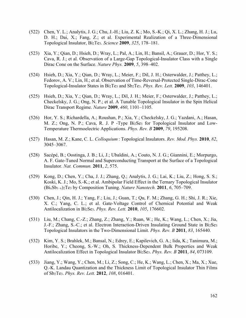
162
(522) Chen, Y. L.; Analytis, J. G.; Chu, J.-H.; Liu, Z. K.; Mo, S.-K.; Qi, X. L.; Zhang, H. J.; Lu,
D. H.; Dai, X.; Fang, Z.; et al. Experimental Realization of a Three-Dimensional
Topological Insulator, Bi2Te3. Science 2009, 325, 178–181.
(523) Xia, Y.; Qian, D.; Hsieh, D.; Wray, L.; Pal, A.; Lin, H.; Bansil, A.; Grauer, D.; Hor, Y. S.;
Cava, R. J.; et al. Observation of a Large-Gap Topological-Insulator Class with a Single
Dirac Cone on the Surface. Nature Phys. 2009, 5, 398–402.
(524) Hsieh, D.; Xia, Y.; Qian, D.; Wray, L.; Meier, F.; Dil, J. H.; Osterwalder, J.; Patthey, L.;
Fedorov, A. V.; Lin, H.; et al. Observation of Time-Reversal-Protected Single-Dirac-Cone
Topological-Insulator States in Bi2Te3 and Sb2Te3. Phys. Rev. Lett. 2009, 103, 146401.
(525) Hsieh, D.; Xia, Y.; Qian, D.; Wray, L.; Dil, J. H.; Meier, F.; Osterwalder, J.; Patthey, L.;
Checkelsky, J. G.; Ong, N. P.; et al. A Tunable Topological Insulator in the Spin Helical
Dirac Transport Regime. Nature 2009, 460, 1101–1105.
(526) Hor, Y. S.; Richardella, A.; Roushan, P.; Xia, Y.; Checkelsky, J. G.; Yazdani, A.; Hasan,
M. Z.; Ong, N. P.; Cava, R. J. P -Type Bi2Se3 for Topological Insulator and Low-
Temperature Thermoelectric Applications. Phys. Rev. B 2009, 79, 195208.
(527) Hasan, M. Z.; Kane, C. L. Colloquium : Topological Insulators. Rev. Mod. Phys. 2010, 82,
3045–3067.
(528) Sacépé, B.; Oostinga, J. B.; Li, J.; Ubaldini, A.; Couto, N. J. G.; Giannini, E.; Morpurgo,
A. F. Gate-Tuned Normal and Superconducting Transport at the Surface of a Topological
Insulator. Nat. Commun. 2011, 2, 575.
(529) Kong, D.; Chen, Y.; Cha, J. J.; Zhang, Q.; Analytis, J. G.; Lai, K.; Liu, Z.; Hong, S. S.;
Koski, K. J.; Mo, S.-K.; et al. Ambipolar Field Effect in the Ternary Topological Insulator
(BixSb1–x)2Te3 by Composition Tuning. Nature Nanotech. 2011, 6, 705–709.
(530) Chen, J.; Qin, H. J.; Yang, F.; Liu, J.; Guan, T.; Qu, F. M.; Zhang, G. H.; Shi, J. R.; Xie,
X. C.; Yang, C. L.; et al. Gate-Voltage Control of Chemical Potential and Weak
Antilocalization in Bi2Se3. Phys. Rev. Lett. 2010, 105, 176602.
(531) Liu, M.; Chang, C.-Z.; Zhang, Z.; Zhang, Y.; Ruan, W.; He, K.; Wang, L.; Chen, X.; Jia,
J.-F.; Zhang, S.-C.; et al. Electron Interaction-Driven Insulating Ground State in Bi2Se3
Topological Insulators in the Two-Dimensional Limit. Phys. Rev. B 2011, 83, 165440.
(532) Kim, Y. S.; Brahlek, M.; Bansal, N.; Edrey, E.; Kapilevich, G. A.; Iida, K.; Tanimura, M.;
Horibe, Y.; Cheong, S.-W.; Oh, S. Thickness-Dependent Bulk Properties and Weak
Antilocalization Effect in Topological Insulator Bi2Se3. Phys. Rev. B 2011, 84, 073109.
(533) Jiang, Y.; Wang, Y.; Chen, M.; Li, Z.; Song, C.; He, K.; Wang, L.; Chen, X.; Ma, X.; Xue,
Q.-K. Landau Quantization and the Thickness Limit of Topological Insulator Thin Films
of Sb2Te3. Phys. Rev. Lett. 2012, 108, 016401.
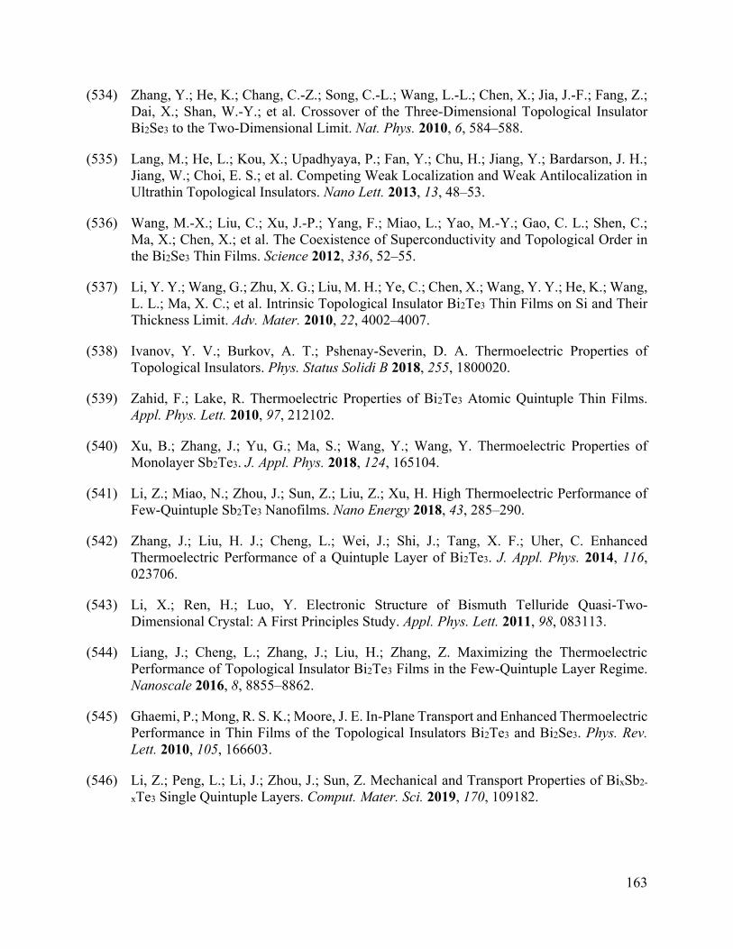
163
(534) Zhang, Y.; He, K.; Chang, C.-Z.; Song, C.-L.; Wang, L.-L.; Chen, X.; Jia, J.-F.; Fang, Z.;
Dai, X.; Shan, W.-Y.; et al. Crossover of the Three-Dimensional Topological Insulator
Bi2Se3 to the Two-Dimensional Limit. Nat. Phys. 2010, 6, 584–588.
(535) Lang, M.; He, L.; Kou, X.; Upadhyaya, P.; Fan, Y.; Chu, H.; Jiang, Y.; Bardarson, J. H.;
Jiang, W.; Choi, E. S.; et al. Competing Weak Localization and Weak Antilocalization in
Ultrathin Topological Insulators. Nano Lett. 2013, 13, 48–53.
(536) Wang, M.-X.; Liu, C.; Xu, J.-P.; Yang, F.; Miao, L.; Yao, M.-Y.; Gao, C. L.; Shen, C.;
Ma, X.; Chen, X.; et al. The Coexistence of Superconductivity and Topological Order in
the Bi2Se3 Thin Films. Science 2012, 336, 52–55.
(537) Li, Y. Y.; Wang, G.; Zhu, X. G.; Liu, M. H.; Ye, C.; Chen, X.; Wang, Y. Y.; He, K.; Wang,
L. L.; Ma, X. C.; et al. Intrinsic Topological Insulator Bi2Te3 Thin Films on Si and Their
Thickness Limit. Adv. Mater. 2010, 22, 4002–4007.
(538) Ivanov, Y. V.; Burkov, A. T.; Pshenay-Severin, D. A. Thermoelectric Properties of
Topological Insulators. Phys. Status Solidi B 2018, 255, 1800020.
(539) Zahid, F.; Lake, R. Thermoelectric Properties of Bi2Te3 Atomic Quintuple Thin Films.
Appl. Phys. Lett. 2010, 97, 212102.
(540) Xu, B.; Zhang, J.; Yu, G.; Ma, S.; Wang, Y.; Wang, Y. Thermoelectric Properties of
Monolayer Sb2Te3. J. Appl. Phys. 2018, 124, 165104.
(541) Li, Z.; Miao, N.; Zhou, J.; Sun, Z.; Liu, Z.; Xu, H. High Thermoelectric Performance of
Few-Quintuple Sb2Te3 Nanofilms. Nano Energy 2018, 43, 285–290.
(542) Zhang, J.; Liu, H. J.; Cheng, L.; Wei, J.; Shi, J.; Tang, X. F.; Uher, C. Enhanced
Thermoelectric Performance of a Quintuple Layer of Bi2Te3. J. Appl. Phys. 2014, 116,
023706.
(543) Li, X.; Ren, H.; Luo, Y. Electronic Structure of Bismuth Telluride Quasi-Two-
Dimensional Crystal: A First Principles Study. Appl. Phys. Lett. 2011, 98, 083113.
(544) Liang, J.; Cheng, L.; Zhang, J.; Liu, H.; Zhang, Z. Maximizing the Thermoelectric
Performance of Topological Insulator Bi2Te3 Films in the Few-Quintuple Layer Regime.
Nanoscale 2016, 8, 8855–8862.
(545) Ghaemi, P.; Mong, R. S. K.; Moore, J. E. In-Plane Transport and Enhanced Thermoelectric
Performance in Thin Films of the Topological Insulators Bi2Te3 and Bi2Se3. Phys. Rev.
Lett. 2010, 105, 166603.
(546) Li, Z.; Peng, L.; Li, J.; Zhou, J.; Sun, Z. Mechanical and Transport Properties of BixSb2-
xTe3 Single Quintuple Layers. Comput. Mater. Sci. 2019, 170, 109182.
164
(547) Li, Z.; Han, S.; Pan, Y.; Miao, N.; Zhou, J.; Xu, H.; Sun, Z. Origin of High Thermoelectric
Performance with a Wide Range of Compositions for BixSb2−xTe3 Single Quintuple
Layers. Phys. Chem. Chem. Phys. 2019, 21, 1315–1323.
(548) Chen, Y.; Wu, Y.; Xu, K.; Ma, C.; Lu, Z.; Zhang, X.; Zhang, H.; Zhu, H.; Fang, Z. New
Sb2Te3– xSex Monolayers with High Electron Mobilities and Wide Absorption Range. ACS
Appl. Mater. Interfaces 2019, 11, 37216–37228.
(549) Sun, Y.; Cheng, H.; Gao, S.; Liu, Q.; Sun, Z.; Xiao, C.; Wu, C.; Wei, S.; Xie, Y. Atomically
Thick Bismuth Selenide Freestanding Single Layers Achieving Enhanced Thermoelectric
Energy Harvesting. J. Am. Chem. Soc. 2012, 134, 20294–20297.
(550) Teweldebrhan, D.; Goyal, V.; Balandin, A. A. Exfoliation and Characterization of Bismuth
Telluride Atomic Quintuples and Quasi-Two-Dimensional Crystals. Nano Lett. 2010, 10,
1209–1218.
(551) Goyal, V.; Teweldebrhan, D.; Balandin, A. A. Mechanically-Exfoliated Stacks of Thin
Films of Bi2Te3 Topological Insulators with Enhanced Thermoelectric Performance. Appl.
Phys. Lett. 2010, 97, 133117.
(552) Hinsche, N. F.; Zastrow, S.; Gooth, J.; Pudewill, L.; Zierold, R.; Rittweger, F.; Rauch, T.;
Henk, J.; Nielsch, K.; Mertig, I. Impact of the Topological Surface State on the
Thermoelectric Transport in Sb2Te3 Thin Films. ACS Nano 2015, 9, 4406–4411.
(553) Guo, M.; Wang, Z.; Xu, Y.; Huang, H.; Zang, Y.; Liu, C.; Duan, W.; Gan, Z.; Zhang, S.-
C.; He, K.; et al. Tuning Thermoelectricity in a Bi2Se3 Topological Insulator via Varied
Film Thickness. New J. Phys. 2016, 18, 015008.
(554) Miao, N.; Zhou, J.; Sa, B.; Xu, B.; Sun, Z. Few-Layer Arsenic Trichalcogenides: Emerging
Two-Dimensional Semiconductors with Tunable Indirect-Direct Band-Gaps. J. Alloys
Compd. 2017, 699, 554–560.
(555) Debbichi, L.; Kim, H.; Björkman, T.; Eriksson, O.; Lebègue, S. First-Principles
Investigation of Two-Dimensional Trichalcogenide and Sesquichalcogenide Monolayers.
Phys. Rev. B 2016, 93, 245307.
(556) Mortazavi, B.; Shojaei, F.; Azizi, M.; Rabczuk, T.; Zhuang, X. As2S3, As2Se3 and As2Te3
Nanosheets: Superstretchable Semiconductors with Anisotropic Carrier Mobilities and
Optical Properties. J. Mater. Chem. C 2020, 8, 2400–2410.
(557) Shelimova, L. E.; Karpinskii, O. G.; Kretova, M. A.; Kosyakov, V. I.; Shestakov, V. A.;
Zemskov, V. S.; Kuznetsov, F. A. Homologous Series of Layered Tetradymite-like
Compounds in the Sb-Te and GeTe-Sb2Te3 Systems. Inorg Mater 2000, 36, 768–775.
(558) Govaerts, K.; Sluiter, M. H. F.; Partoens, B.; Lamoen, D. Stability of Sb-Te Layered
Structures: First-Principles Study. Phys. Rev. B 2012, 85, 144114.

165
(559) Semiletov, S.; Pinsker, Z. The Electron Diffraction Analysis of the System of Alloys Bi-
Se. In Dokl. AN SSSR 1955, 100, 1079–1082.
(560) Lind, H.; Lidin, S.; Häussermann, U. Structure and Bonding Properties of (Bi2Se3)m(Bi2)n
Stacks by First-Principles Density Functional Theory. Phys. Rev. B 2005, 72, 184101.
(561) Lind, H.; Lidin, S. A General Structure Model for Bi–Se Phases Using a Superspace
Formalism. Solid State Sciences 2003, 5, 47–57.
(562) Cook, N. J.; Ciobanu, C. L.; Wagner, T.; Stanley, C. J. Minerals of the System Bi-Te-Se-
S Related to the Tetradymite Archetype: Review of Classification and Compositional
Variation. The Canadian Mineralogist 2007, 45, 665–708.
(563) Stasova, M. Crystal Structure of Bismuth Selenides and Bismuth and Antimony Tellurides.
J. Struct. Chem. 1967, 8, 584–589.
(564) Ciobanu, C. L.; Pring, A.; Cook, N. J.; Self, P.; Jefferson, D.; Dima, G. I.; Melnikov, V.
Chemical-Structural Modularity in the Tetradymite Group: A HRTEM Study. American
Mineralogist 2009, 94, 517–534.
(565) Samanta, M.; Pal, K.; Waghmare, U. V.; Biswas, K. Intrinsically Low Thermal
Conductivity and High Carrier Mobility in Dual Topological Quantum Material, N‐Type
BiTe. Angew. Chem. Int. Ed. 2020, 59, 4822–4829.
(566) Brebrick, R. F. Characterization of Phases in the 50–60 at. % Te Region of the Bi–Te
System by X-Ray Powder Diffraction Patterns. J Appl Crystallogr 1968, 1, 241–246.
(567) Agafonov, V.; Rodier, N.; Céolin, R.; Bellissent, R.; Bergman, C.; Gaspard, J. P. Structure
of Sb2Te. Acta Crystallogr. C Cryst. Struct. Commun. 1991, 47, 1141–1143.
(568) Bos, J. W. G.; Zandbergen, H. W.; Lee, M.-H.; Ong, N. P.; Cava, R. J. Structures and
Thermoelectric Properties of the Infinitely Adaptive Series ( Bi2)m(Bi2Te3)n. Phys. Rev. B
2007, 75, 195203.
(569) Stillwell, R. L.; Jenei, Z.; Weir, S. T.; Vohra, Y. K.; Jeffries, J. R. Superconducting Bi2Te:
Pressure-Induced Universality in the (Bi2)m(Bi2Te3)n Series. Phys. Rev. B 2016, 93,
094511.
(570) Cecchi, S.; Dragoni, D.; Kriegner, D.; Tisbi, E.; Zallo, E.; Arciprete, F.; Holý, V.;
Bernasconi, M.; Calarco, R. Interplay between Structural and Thermoelectric Properties in
Epitaxial Sb2+xTe3 Alloys. Adv. Funct. Mater. 2019, 29, 1805184.
(571) Stasova, M. The Crystal Structure of Bismuthum Selenide Bi4Se3. Izvestiya Akad Nauk
SSSR Neorg Materialy 1968, 4, 28–31.
(572) Yamana, K.; Kihara, K.; Matsumoto, T. Bismuth Tellurides: BiTe and Bi4Te3. Acta
Crystallogr. B Struct. Sci. 1979, 35, 147–149.

166
(573) Khalil, L.; Papalazarou, E.; Caputo, M.; Nilforoushan, N.; Perfetti, L.; Taleb-Ibrahimi, A.;
Kandyba, V.; Barinov, A.; Gibson, Q. D.; Cava, R. J.; et al. Electronic Band Structure for
Occupied and Unoccupied States of the Natural Topological Superlattice Phase Sb2Te.
Phys. Rev. B 2017, 95, 085118.
(574) Johannsen, J. C.; Autès, G.; Crepaldi, A.; Moser, S.; Casarin, B.; Cilento, F.; Zacchigna,
M.; Berger, H.; Magrez, A.; Bugnon, Ph.; et al. Engineering the Topological Surface States
in the (Sb2)m−Sb2Te3 (m = 0–3) Superlattice Series. Phys. Rev. B 2015, 91, 201101.
(575) Eschbach, M.; Lanius, M.; Niu, C.; Młyńczak, E.; Gospodarič, P.; Kellner, J.; Schüffelgen,
P.; Gehlmann, M.; Döring, S.; Neumann, E.; et al. BiTe Is a Dual Topological Insulator.
Nat. Commun. 2017, 8, 14976.
(576) Poudeu, P. F. P.; Kanatzidis, M. G. Design in Solid State Chemistry Based on Phase
Homologies. Sb4Te3 and Sb8Te9 as New Members of the Series (Sb2Te3)m·(Sb2)n. Chem.
Commun. 2005, 21, 2672.
(577) Kifune, K.; Kubota, Y.; Matsunaga, T.; Yamada, N. Extremely Long Period-Stacking
Structure in the Sb–Te Binary System. Acta Crystallogr. B Struct. Sci. 2005, 61, 492–497.
(578) Takagaki, Y.; Giussani, A.; Tominaga, J.; Jahn, U.; Calarco, R. Transport Properties in a
Sb–Te Binary Topological-Insulator System. J. Phys.: Condens. Matter 2013, 25, 345801.
(579) Govaerts, K.; Park, K.; De Beule, C.; Partoens, B.; Lamoen, D. Effect of Bi Bilayers on
the Topological States of Bi2Se3: A First-Principles Study. Phys. Rev. B 2014, 90, 155124.
(580) Gibson, Q. D.; Schoop, L. M.; Weber, A. P.; Ji, H.; Nadj-Perge, S.; Drozdov, I. K.;
Beidenkopf, H.; Sadowski, J. T.; Fedorov, A.; Yazdani, A.; et al. Termination-Dependent
Topological Surface States of the Natural Superlattice Phase Bi4Se3. Phys. Rev. B 2013,
88, 081108.
(581) Chagas, T.; Ribeiro, G. A. S.; Gonçalves, P. H. R.; Calil, L.; Silva, W. S.; Malachias, Â.;
Mazzoni, M. S. C.; Magalhães-Paniago, R. Bi2:Bi2Te3 Stacking Influence on the Surface
Electronic Response of the Topological Insulator Bi4Te3. Electron. Struct. 2020, 2,
015002.
(582) Rodrigues-Junior, G.; Marçal, L. A. B.; Ribeiro, G. A. S.; Rappl, P. H. de O.; Abramof,
E.; Sciammarella, P. V.; Guimarães, L. de M.; Pérez, C. A.; Malachias, Â. Direct
Observation of Large Strain through van der Waals Gaps on Epitaxial Bi2Te3/Graphite:
Pseudomorphic Relaxation and the Role of Bi2 Layers on the BixTey Topological Insulator
Series. Phys. Rev. Materials 2020, 4, 023602.
(583) Zallen, R.; Drews, R. E.; Emerald, R. L.; Slade, M. L. Electronic Structure of Crystalline
and Amorphous As2S3 and As2Se3. Phys. Rev. Lett. 1971, 26, 1564–1567.
(584) Blossey, D. F.; Zallen, R. Surface and Bulk Photoresponse of Crystalline As2S3. Phys. Rev.
B 1974, 9, 4306–4313.
167
(585) Zallen, R.; Blossey, D. F. The Optical Properties, Electronic Structure, and
Photoconductivity of Arsenic Chalcogenide Layer Crystals. In Optical and Electrical
Properties; Springer, 1976; pp. 231–272.
(586) Schein, L. B. Temperature Independent Drift Mobility along the Molecular Direction of
As2S3. Phys. Rev. B 1977, 15, 1024–1034.
(587) Mohammed, L.; Saeed, M. A.; Zhang, Q.; Musa, A. Core-Level Excitation in Polymorph
of As2S3 and β-In2S3. J. Comput. Phys. 2018, 28, 11–17.
(588) Wu, C.-C. Structure and Optical Characterization of Sulfur Incorporated As2Se3 Crystals.
J. Appl. Phys. 2007, 101, 063533.
(589) Deng, H. Theoretical Prediction of the Structural, Electronic, Mechanical and
Thermodynamic Properties of the Binary α-As2Te3 and β-As2Te3. J. Alloys Compd. 2016,
656, 695–701.
(590) Vaney, J.-B.; Crivello, J.-C.; Morin, C.; Delaizir, G.; Carreaud, J.; Piarristeguy, A.;
Monnier, J.; Alleno, E.; Pradel, A.; Lopes, E. B.; et al. Electronic Structure, Low-
Temperature Transport and Thermodynamic Properties of Polymorphic β-As2Te3. RSC
Adv. 2016, 6, 52048–52057.
(591) Kim, H.-S.; Heinz, N. A.; Gibbs, Z. M.; Tang, Y.; Kang, S. D.; Snyder, G. J. High
Thermoelectric Performance in (Bi0.25Sb0.75)2Te3 Due to Band Convergence and Improved
by Carrier Concentration Control. Materials Today 2017, 20, 452–459.
(592) Sehr, R.; Testardi, L. R. The Optical Properties of P-Type Bi2Te3-Sb2Te3 Alloys between
2–15 Microns. J. Phys. Chem. Solids 1962, 23, 1219–1224.
(593) Stordeur, M.; Stölzer, M.; Sobotta, H.; Riede, V. Investigation of the Valence Band
Structure of Thermoelectric (Bi1−xSbx)2Te3 Single Crystals. Phys. Stat. Sol. B 1988, 150,
165–176.
(594) Jacobs-Gedrim, R. B.; Murphy, M. T.; Yang, F.; Jain, N.; Shanmugam, M.; Song, E. S.;
Kandel, Y.; Hesamaddin, P.; Yu, H. Y.; Anantram, M. P.; et al. Reversible Phase-Change
Behavior in Two-Dimensional Antimony Telluride (Sb2Te3) Nanosheets. Appl. Phys. Lett.
2018, 112, 133101.
(595) Xu, B.; Cao, Y.; An, X.; Zhang, J.; Ma, S.; Wang, Y.; Chen, J.; Chen, L.; Yi, L. Electronic
and Optical Properties of Monolayer Sb2Te3 Using Biaxial Strain. J. Phys. Soc. Jpn. 2019,
88, 124712.
(596) Kang, Y.; Zhang, Q.; Fan, C.; Hu, W.; Chen, C.; Zhang, L.; Yu, F.; Tian, Y.; Xu, B. High
Pressure Synthesis and Thermoelectric Properties of Polycrystalline Bi2Se3. J. Alloys
Compd. 2017, 700, 223–227.
168
(597) Butch, N. P.; Kirshenbaum, K.; Syers, P.; Sushkov, A. B.; Jenkins, G. S.; Drew, H. D.;
Paglione, J. Strong Surface Scattering in Ultrahigh-Mobility Bi2Se3 Topological Insulator
Crystals. Phys. Rev. B 2010, 81, 241301.
(598) Sapkota, Y. R.; Alkabsh, A.; Walber, A.; Samassekou, H.; Mazumdar, D. Optical Evidence
for Blue Shift in Topological Insulator Bismuth Selenide in the Few-Layer Limit. Appl.
Phys. Lett. 2017, 110, 181901.
(599) Yazyev, O. V.; Kioupakis, E.; Moore, J. E.; Louie, S. G. Quasiparticle Effects in the Bulk
and Surface-State Bands of Bi2Se3 and Bi2Te3 Topological Insulators. Phys. Rev. B 2012,
85, 161101.
(600) Usanov, D.; Nezhdanov, A.; Kudryashov, M.; Krivenkov, I.; Markelov, A.; Trushin, V.;
Mochalov, L.; Gogova, D.; Mashin, A. Some Insights into the Mechanism of
Photoluminescence of As-S-Based Films Synthesized by PECVD. J. Non-Cryst. Solids
2019, 513, 120–124.
(601) Ginley, T.; Wang, Y.; Law, S. Topological Insulator Film Growth by Molecular Beam
Epitaxy: A Review. Crystals 2016, 6, 154.
(602) Springholz, G.; Wimmer, S.; Groiss, H.; Albu, M.; Hofer, F.; Caha, O.; Kriegner, D.;
Stangl, J.; Bauer, G.; Holý, V. Structural Disorder of Natural BimSen Superlattices Grown
by Molecular Beam Epitaxy. Phys. Rev. Materials 2018, 2, 054202.
(603) Steiner, H.; Volobuev, V.; Caha, O.; Bauer, G.; Springholz, G.; Holý, V. Structure and
Composition of Bismuth Telluride Topological Insulators Grown by Molecular Beam
Epitaxy. J. Appl. Crystallogr. 2014, 47, 1889–1900.
(604) Heo, H.; Sung, J. H.; Ahn, J.-H.; Ghahari, F.; Taniguchi, T.; Watanabe, K.; Kim, P.; Jo,
M.-H. Frank-van der Merwe Growth versus Volmer-Weber Growth in Successive
Stacking of a Few-Layer Bi2Te3/Sb2Te3 by van der Waals Heteroepitaxy: The Critical
Roles of Finite Lattice-Mismatch with Seed Substrates. Adv. Electron. Mater. 2017, 3.
1600375.
(605) Liu, M.; Liu, F. Y.; Man, B. Y.; Bi, D.; Xu, X. Y. Multi-Layered Nanostructure Bi2Se3
Grown by Chemical Vapor Deposition in Selenium-Rich Atmosphere. Appl. Surf. Sci.
2014, 317, 257–261.
(606) Venkatasubramanian, R.; Colpitts, T.; Watko, E.; Lamvik, M.; ElMasry, N. MOCVD of
Bi2Te3, Sb2Te3 and Their Superlattice Structures for Thin-Film Thermoelectric
Applications. J. Cryst. Growth 1997, 170, 817–821.
(607) Alegria, L. D.; Schroer, M. D.; Chatterjee, A.; Poirier, G. R.; Pretko, M.; Patel, S. K.; Petta,
J. R. Structural and Electrical Characterization of Bi2Se3 Nanostructures Grown by Metal-
Organic Chemical Vapor Deposition. Nano Lett. 2012, 12, 4711–4714.
(608) Giani, A.; Boulouz, A.; Pascal-Delannoy, F.; Foucaran, A.; Charles, E.; Boyer, A. Growth
of Bi2Te3 and Sb2Te3 Thin Films by MOCVD. Mat. Sci. Eng. B-Solid 1999, 64, 19–24.
169
(609) Kuznetsov, P. I.; Shchamkhalova, B. S.; Yapaskurt, V. O.; Shcherbakov, V. D.; Luzanov,
V. A.; Yakushcheva, G. G.; Jitov, V. A.; Sizov, V. E. MOVPE Deposition of Sb2Te3 and
Other Phases of Sb-Te System on Sapphire Substrate. J. Cryst. Growth 2017, 471, 1–7.
(610) Hilmi, I.; Lotnyk, A.; Gerlach, J. W.; Schumacher, P.; Rauschenbach, B. Research Update:
Van-Der-Waals Epitaxy of Layered Chalcogenide Sb2Te3 Thin Films Grown by Pulsed
Laser Deposition. APL Materials 2017, 5, 050701.
(611) Dauscher, A.; Thomy, A.; Scherrer, H. Pulsed Laser Deposition of Bi2Te3 Thin Films. Thin
Solid Films 1996, 280, 61–66.
(612) Bailini, A.; Donati, F.; Zamboni, M.; Russo, V.; Passoni, M.; Casari, C. S.; Li Bassi, A.;
Bottani, C. E. Pulsed Laser Deposition of Bi2Te3 Thermoelectric Films. Appl. Surf. Sci.
2007, 254, 1249–1254.
(613) Concepción, O.; Galván-Arellano, M.; Torres-Costa, V.; Climent-Font, A.; Bahena, D.;
Manso Silván, M.; Escobosa, A.; de Melo, O. Controlling the Epitaxial Growth of Bi2Te3,
BiTe, and Bi4Te3 Pure Phases by Physical Vapor Transport. Inorg. Chem. 2018, 57,
10090–10099.
(614) Kim, D.-H.; Byon, E.; Lee, G.-H.; Cho, S. Effect of Deposition Temperature on the
Structural and Thermoelectric Properties of Bismuth Telluride Thin Films Grown by Co-
Sputtering. Thin Solid Films 2006, 510, 148–153.
(615) Saito, Y.; Fons, P.; Makino, K.; Mitrofanov, K. V.; Uesugi, F.; Takeguchi, M.; Kolobov,
A. V.; Tominaga, J. Compositional Tuning in Sputter-Grown Highly-Oriented Bi–Te
Films and Their Optical and Electronic Structures. Nanoscale 2017, 9, 15115–15121.
(616) Akshay, V. R.; Suneesh, M. V.; Vasundhara, M. Tailoring Thermoelectric Properties
through Structure and Morphology in Chemically Synthesized N-Type Bismuth Telluride
Nanostructures. Inorg. Chem. 2017, 56, 6264–6274.
(617) Rotunno, E.; Longo, M.; Wiemer, C.; Fallica, R.; Campi, D.; Bernasconi, M.; Lupini, A.
R.; Pennycook, S. J.; Lazzarini, L. A Novel Sb2Te3 Polymorph Stable at the Nanoscale.
Chem. Mater. 2015, 27, 4368–4373.
(618) Kirkinskii, V.; Yakushev, V. A New Polymorphic Modification of Arsenic Selenide
Obtained at High Presssures. In Doklady Chemistry; 1968; Vol. 182, p. 896.
(619) Lityagina, L. M.; Kulikova, L. F.; Zibrov, I. P.; Dyuzheva, T. I.; Nikolaev, N. A.; Brazhkin,
V. V. Structural Transformations in the As–Se System under High Pressures and
Temperatures. J. Alloys Compd. 2015, 644, 799–803.
(620) Bolotina, N. B.; Brazhkin, V. V.; Dyuzheva, T. I.; Katayama, Y.; Kulikova, L. F.;
Lityagina, L. V.; Nikolaev, N. A. High-Pressure Polymorphism of As2S3 and New AsS2
Modification with Layered Structure. Jetp Lett. 2014, 98, 539–543.

170
(621) Brazhkin, V. V.; Bolotina, N. B.; Dyuzheva, T. I.; Gavriliuk, A. G.; Lyapin, A. G.; Popova,
S. V.; Samulski, S. AsS Layered-Structure Compound: New Kind of Covalent Crystals.
CrystEngComm 2011, 13, 2599.
(622) Bolotina, N. B.; Brazhkin, V. V.; Dyuzheva, T. I.; Lityagina, L. M.; Kulikova, L. F.;
Nikolaev, N. A.; Verin, I. A. Crystal Structure of New AsS2 Compound. Crystallogr. Rep.
2013, 58, 61–64.
(623) Scheidemantel, T. J.; Meng, J. F.; Badding, J. V. Thermoelectric Power and Phase
Transition of Polycrystalline As2Te3 under Pressure. J. Phys. Chem. Solids 2005, 66, 1744–
1747.
(624) Zhao, J.; Yang, L.; Yu, Z.; Wang, Y.; Li, C.; Yang, K.; Liu, Z.; Wang, Y. Structural Phase
Transitions and Metallized Phenomena in Arsenic Telluride under High Pressure. Inorg.
Chem. 2016, 55, 3907–3914.
(625) Cuenca-Gotor, V. P.; Sans, J. A.; Ibáñez, J.; Popescu, C.; Gomis, O.; Vilaplana, R.;
Manjón, F. J.; Leonardo, A.; Sagasta, E.; Suárez-Alcubilla, A.; et al. Structural,
Vibrational, and Electronic Study of α-As2Te3 under Compression. J. Phys. Chem. C 2016,
120, 19340–19352.
(626) Manjón, F. J.; Vilaplana, R.; Gomis, O.; Pérez-González, E.; Santamaría-Pérez, D.; Marín-
Borrás, V.; Segura, A.; González, J.; Rodríguez-Hernández, P.; Muñoz, A.; et al. High-
Pressure Studies of Topological Insulators Bi2Se3, Bi2Te3, and Sb2Te3. Phys. Status Solidi
B 2013, 250, 669–676.
(627) Morozova, N. V.; Korobeinikov, I. V.; Ovsyannikov, S. V. Strategies and Challenges of
High-Pressure Methods Applied to Thermoelectric Materials. J. Appl. Phys. 2019, 125,
220901.
(628) Bera, A.; Pal, K.; Muthu, D. V. S.; Waghmare, U. V.; Sood, A. K. Pressure-Induced Phase
Transition in Bi2Se3 at 3 GPa: Electronic Topological Transition or Not? J. Phys.:
Condens. Matter 2016, 28, 105401.
(629) Zhu, H.; Dong, J.; Li, P.; Wang, Y.; Guo, Z.; Shan, X.; Gong, Y.; An, P.; Li, X.; Zhang,
J.; et al. Bi-Centric View of the Isostructural Phase Transitions in α-Bi2Se3 and α-Bi2Te3:
Bi-Centric View of Isostructural Phase Transitions in Bi2Se3 and Bi2Te3. Phys. Status
Solidi B 2017, 254, 1700007.
(630) Serebryanaya, N.; Tatyanin, E.; Buga, S.; Kruglov, I.; Lvova, N.; Blank, V. Monoclinic
Structure and Electrical Properties of Metastable Sb2Te3 and Bi0.4Sb1.6Te3 Phases:
Structure and Properties of Metastable Sb2Te3 and Bi0.4Sb1.6Te3 Phases. Phys. Status Solidi
B 2015, 252, 267–273.
(631) Buga, S. G.; Serebryanaya, N. R.; Dubitskiy, G. A.; Semenova, E. E.; Aksenenkov, V. V.;
Blank, V. D. Structure and Electrical Properties of Sb2Te3 and Bi0.4Sb1.6Te3 Metastable
Phases Obtained by HPHT Treatment. High Pressure Research 2011, 31, 86–90.

171
(632) Kulbachinskii, V. A.; Buga, S. G.; Serebryanaya, N. R.; Perov, N. S.; Kytin, V. G.;
Tarelkin, S. A.; Bagramov, R. H.; Eliseev, N. N.; Blank, V. D. Superconductivity,
Magnetoresistance, Magnetic Anomaly and Crystal Structure of New Phases of
Topological Insulators Bi2Se3 and Sb2Te3. J. Phys.: Conf. Ser. 2018, 969, 012152.
(633) Buga, S. G.; Kulbachinskii, V. A.; Kytin, V. G.; Kytin, G. A.; Kruglov, I. A.; Lvova, N.
A.; Perov, N. S.; Serebryanaya, N. R.; Tarelkin, S. A.; Blank, V. D. Superconductivity in
Bulk Polycrystalline Metastable Phases of Sb2Te3 and Bi2Te3 Quenched after High-
Pressure–High-Temperature Treatment. Chem. Phys. Lett. 2015, 631–632, 97–102.
(634) Yamamoto, A.; Hashizume, D.; Bahramy, M. S.; Tokura, Y. Coexistence of
Monochalocogen and Dichalocogen Ions in BiSe2 and BiS2 Crystals Prepared at High
Pressure. Inorg. Chem. 2015, 54, 4114–4119.
(635) Kevy, S. M.; Nielsen, M. B.; Lundegaard, L. F.; Ceresoli, D.; Chen, Y.-S.; Reardon, H.;
Parisiades, P.; Bremholm, M. Investigation of the High Pressure Phase BiS2: Temperature-
Resolved Structure and Compression Behavior to 60 GPa. J. Alloys Compd. 2019, 789,
588–594.
(636) Cisar, A.; Corbett, J. D.; Daake, R. L. The Zirconium Dichloride Phase Region. Synthesis,
Structure, and Photoelectron Spectral Studies of 3R-ZrCl2, 6T-Zr1.05Cl2, and Related
Phases. Inorg. Chem. 1979, 18, 836–843.
(637) Guthrie, D. H.; Corbett, J. D. Synthesis and Structure of an Infinite-Chain Form of ZrI2
(α). Journal of Solid State Chemistry 1981, 37, 256–263.
(638) Corbett, J. D.; Guthrie, D. H. A Second Infinite-Chain Form of Zirconium Diiodide (β)
and Its Coherent Intergrowth with α-Zirconium Diiodide. Inorg. Chem. 1982, 21, 1747–
1751.
(639) Baskurt, M.; Eren, I.; Yagmurcukardes, M.; Sahin, H. Vanadium Dopant- and Strain-
Dependent Magnetic Properties of Single-Layer VI3. Appl. Surf. Sci. 2020, 508, 144937.
(640) Kong, T.; Stolze, K.; Timmons, E. I.; Tao, J.; Ni, D.; Guo, S.; Yang, Z.; Prozorov, R.;
Cava, R. J. VI3 — A New Layered Ferromagnetic Semiconductor. Adv. Mater. 2019, 31,
1808074.
(641) Gati, E.; Inagaki, Y.; Kong, T.; Cava, R. J.; Furukawa, Y.; Canfield, P. C.; Bud’ko, S. L.
Multiple Ferromagnetic Transitions and Structural Distortion in the van der Waals
Ferromagnet VI3 at Ambient and Finite Pressures. Phys. Rev. B 2019, 100, 094408.
(642) Kong, T.; Guo, S.; Ni, D.; Cava, R. J. Crystal Structure and Magnetic Properties of the
Layered van der Waals Compound VBr3. Phys. Rev. Materials 2019, 3, 084419.
(643) Kulish, V. V.; Huang, W. Single-Layer Metal Halides MX2 (X = Cl, Br, I): Stability and
Tunable Magnetism from First Principles and Monte Carlo Simulations. J. Mat. Chem. C
2017, 5, 8734–8741.

172
(644) Chen, P.; Zou, J.-Y.; Liu, B.-G. Intrinsic Ferromagnetism and Quantum Anomalous Hall
Effect in a CoBr2 Monolayer. Phys. Chem. Chem. Phys. 2017, 19, 13432–13437.
(645) Ashton, M.; Gluhovic, D.; Sinnott, S. B.; Guo, J.; Stewart, D. A.; Hennig, R. G. Two-
Dimensional Intrinsic Half-Metals With Large Spin Gaps. Nano Lett. 2017, 17, 5251–
5257.
(646) Zhang, W. B.; Qu, Q.; Zhu, P.; Lam, C. H. Robust Intrinsic Ferromagnetism and Half
Semiconductivity in Stable Two-Dimensional Single-Layer Chromium Trihalides. J.
Mater. Chem. C 2015, 3, 12457–12468.
(647) McGuire, M. A. Crystal and Magnetic Structures in Layered, Transition Metal Dihalides
and Trihalides. Crystals 2017, 7, 121.
(648) McGuire, M. A.; Dixit, H.; Cooper, V. R.; Sales, B. C. Coupling of Crystal Structure and
Magnetism in the Layered, Ferromagnetic Insulator CrI3. Chem. Mater. 2015, 27, 612–
620.
(649) Mashhadi, S.; Weber, D.; Schoop, L. M.; Schulz, A.; Lotsch, B. V.; Burghard, M.; Kern,
K. Electrical Transport Signature of the Magnetic Fluctuation-Structure Relation in α-
RuCl3 Nanoflakes. Nano Lett. 2018, 18, 3203–3208.
(650) Klein, D. R.; MacNeill, D.; Song, Q.; Larson, D. T.; Fang, S.; Xu, M.; Ribeiro, R. A.;
Canfield, P. C.; Kaxiras, E.; Comin, R.; et al. Enhancement of Interlayer Exchange in an
Ultrathin Two-Dimensional Magnet. Nat. Phys. 2019, 15, 1255–1260.
(651) Bengel, H.; Cantow, H.-J.; Magonov, S. N.; Hillebrecht, H.; Thiele, G.; Liang, W.;
Whangbo, M.-H. Tip-Force Induced Surface Corrugation in Layered Transition Metal
Trichlorides MCl3 (M = Ru, Mo, Rh, Ir). Surf. Sci. 1995, 343, 95–103.
(652) Thiel, L.; Wang, Z.; Tschudin, M. A.; Rohner, D.; Gutierrez-Lezama, I.; Ubrig, N.;
Gibertini, M.; Giannini, E.; Morpurgo, A. F.; Maletinsky, P. Probing Magnetism in 2D
Materials at the Nanoscale with Single-Spin Microscopy. Science 2019, 364, 973–976.
(653) Shcherbakov, D.; Stepanov, P.; Weber, D.; Wang, Y.; Hu, J.; Zhu, Y.; Watanabe, K.;
Taniguchi, T.; Mao, Z.; Windl, W.; et al. Raman Spectroscopy, Photocatalytic
Degradation, and Stabilization of Atomically Thin Chromium Tri-Iodide. Nano Lett. 2018,
18, 4214–4219.
(654) Li, X.; Zhang, Z.; Zhang, H. High Throughput Study on Magnetic Ground States with
Hubbard U Corrections in Transition Metal Dihalide Monolayers. Nanoscale Adv. 2020,
2, 495–501.
(655) Hu, H.; Tong, W.-Y.; Shen, Y.-H.; Wan, X.; Duan, C.-G. Concept of the Half-Valley-
Metal and Quantum Anomalous Valley Hall Effect. npj Computational Materials 2020, 6,
129.
173
(656) Kong, X.; Li, L.; Liang, L.; Peeters, F. M.; Liu, X.-J. The Magnetic, Electronic, and Light-
Induced Topological Properties in Two-Dimensional Hexagonal FeX2 (X = Cl, Br, I)
Monolayers. Appl. Phys. Lett. 2020, 116, 192404.
(657) Zhao, P.; Ma, Y.; Wang, H.; Huang, B.; Kou, L.; Dai, Y. Intrinsic Valley Polarization and
Anomalous Valley Hall Effect in Single-Layer 2H-FeCl2. 2020, arXiv:2003.04561.
(658) Zhou, X.; Brzostowski, B.; Durajski, A.; Liu, M.; Xiang, J.; Jiang, T.; Wang, Z.; Chen, S.;
Li, P.; Zhong, Z.; et al. Atomically Thin 1T-FeCl2 Grown by Molecular-Beam Epitaxy. J.
Phys. Chem. C 2020, 124, 9416–9423.
(659) Tracy, J. W.; Gregory, N. W.; Lingafelter, E. C. Crystal Structure of Chromium(II)
Bromide. Acta Cryst 1962, 15, 672–674.
(660) Tracy, J. W.; Gregory, N. W.; Stewart, J. M.; Lingafelter, E. C. The Crystal Structure of
Chromium(II) Iodide. Acta Cryst 1962, 15, 460–463.
(661) Li, P.; Wang, C.; Zhang, J.; Chen, S.; Guo, D.; Ji, W.; Zhong, D. Single-Layer CrI3 Grown
by Molecular Beam Epitaxy. Science Bulletin 2020, 65, 1064–1071.
(662) Peng, L.; Zhao, J.; Cai, M.; Hua, G.-Y.; Liu, Z.-Y.; Xia, H.-N.; Yuan, Y.; Zhang, W.-H.;
Xu, G.; Zhao, L.-X.; et al. Mott Phase in a van der Waals Transition-Metal Halide at
Single-Layer Limit. Phys. Rev. Research 2020, 2, 023264.
(663) Niel, M.; Cros, C.; Le Flem, G.; Pouchard, M.; Hagenmuller, P. Magnetic Behaviour of
Vanadium +II in One- and Two-Dimensional Systems. Physica B+C 1977, 86–88, 702–
704.
(664) Hirakawa, K.; Kadowaki, H.; Ubukoshi, K. Study of Frustration Effects in Two-
Dimensional Triangular Lattice Antiferromagnets–Neutron Powder Diffraction Study of
VX2 , X≡Cl, Br and I. J. Phys. Soc. Jpn. 1983, 52, 1814–1824.
(665) Kadowaki, H.; Ubukoshi, K.; Hirakawa, K.; L. Martínez, J.; Shirane, G. Experimental
Study of New Type Phase Transition in Triangular Lattice Antiferromagnet VCl2. J. Phys.
Soc. Jpn. 1987, 56, 4027–4039.
(666) Kadowaki, H.; Ubukoshi, K.; Hirakawa, K. Neutron Scattering Study of the Triangular-
Lattice Antiferromagnet VBr2. J. Phys. Soc. Jpn. 1985, 54, 363–373.
(667) Abdul Wasey, A. H. M.; Karmakar, D.; Das, G. P. Manifestation of Long-Range Ordered
State in Layered VX2 (X = Cl, Br, I) Systems. J. Phys.: Condens. Matter 2013, 25, 476001.
(668) Sato, T.; Kadowaki, H.; Iio, K. Successive Phase Transitions in the Hexagonal-Layered
Heisenberg Antiferromagnets MnX2 (X = Br, I). Physica B: Condensed Matter 1995, 213–
214, 224–226.
174
(669) Park, J.; Ryu, S.; Han, M.; Oh, S.-J. Charge-Transfer Satellites in the 2 p Core-Level
Photoelectron Spectra of Heavy-Transition-Metal Dihalides. Phys. Rev. B 1988, 37,
10867–10875.
(670) Gelard, J.; Fert, A. R.; Meriel, P.; Allain, Y. Magnetic Structure of FeI2 by Neutron
Diffraction Experiments. Solid State Commun. 1974, 14, 187–189.
(671) Katsumata, K.; Katori, H. A.; Kimura, S.; Narumi, Y.; Hagiwara, M.; Kindo, K. Phase
Transition of a Triangular Lattice Ising Antiferromagnet FeI2. Phys. Rev. B 2010, 82,
104402.
(672) Wilkinson, M. K.; Cable, J. W.; Wollan, E. O.; Koehler, W. C. Neutron Diffraction
Investigations of the Magnetic Ordering in Fe Br2, CoBr2, FeCl2, and CoCl2. Phys. Rev.
1959, 113, 497–507.
(673) Starr, C.; Bitter, F.; Kaufmann, A. R. The Magnetic Properties of the Iron Group
Anhydrous Chlorides at Low Temperatures. I. Experimental. Phys. Rev. 1940, 58, 977–
983.
(674) Cable, J. W.; Wilkinson, M. K.; Wollan, E. O.; Koehler, W. C. Neutron Diffraction
Investigation of the Magnetic Order in MnI2. Phys. Rev. 1962, 125, 1860–1864.
(675) Utesov, O. I.; Syromyatnikov, A. V. Cascades of Phase Transitions in Spiral Magnets
Caused by Dipolar Forces. Phys. Rev. B 2017, 95, 214420.
(676) Kurumaji, T.; Seki, S.; Ishiwata, S.; Murakawa, H.; Tokunaga, Y.; Kaneko, Y.; Tokura, Y.
Magnetic-Field Induced Competition of Two Multiferroic Orders in a Triangular-Lattice
Helimagnet MnI2. Phys. Rev. Lett. 2011, 106, 167206.
(677) Kuindersma, S. R.; Sanchez, J. P.; Haas, C. Magnetic and Structural Investigations on NiI2
and CoI2. Physica B+C 1981, 111, 231–248.
(678) Mekata, M.; Kuriyama, H.; Ajiro, Y.; Mitsuda, S.; Yoshizawa, H. First-Order Magnetic
Transition in CoI2. J. Magn. Magn. Mater. 1992, 104–107, 859–860.
(679) Kurumaji, T.; Seki, S.; Ishiwata, S.; Murakawa, H.; Kaneko, Y.; Tokura, Y.
Magnetoelectric Responses Induced by Domain Rearrangement and Spin Structural
Change in Triangular-Lattice Helimagnets NiI2 and CoI2. Phys. Rev. B 2013, 87, 014429.
(680) Chen, A. L.; Yu, P. Y.; Taylor, R. D. Closure of the Charge-Transfer Energy Gap and
Metallization of NiI2 under Pressure. Phys. Rev. Lett. 1993, 71, 4011–4014.
(681) Adam, A.; Billerey, D.; Terrier, C.; Mainard, R.; Regnault, L. P.; Rossat-Mignod, J.;
Mériel, P. Neutron Diffraction Study of the Commensurate and Incommensurate Magnetic
Structures of NiBr2. Solid State Commun. 1980, 35, 1–5.
175
(682) Day, P.; Dinsdale, A.; Krausz, E. R.; Robbins, D. J. Optical and Neutron Diffraction Study
of the Magnetic Phase Diagram of NiBr2. J. Phys. C: Solid State Phys. 1976, 9, 2481–
2490.
(683) Day, P.; Ziebeck, K. R. A. Incommensurate Spin Structure in the Low-Temperature
Magnetic Phase of NiBr2. J. Phys. C: Solid State Phys. 1980, 13, L523–L525.
(684) Babu, S.; Prokes, K.; Huang, Y. K.; Radu, F.; Mishra, S. K. Magnetic-Field-Induced
Incommensurate to Collinear Spin Order Transition in NiBr2. J. Appl. Phys. 2019, 125,
093902.
(685) Tokunaga, Y.; Okuyama, D.; Kurumaji, T.; Arima, T.; Nakao, H.; Murakami, Y.; Taguchi,
Y.; Tokura, Y. Multiferroicity in NiBr2 with Long-Wavelength Cycloidal Spin Structure
on a Triangular Lattice. Phys. Rev. B 2011, 84, 060406.
(686) Torun, E.; Sahin, H.; Singh, S. K.; Peeters, F. M. Stable Half-Metallic Monolayers of
FeCl2. Appl. Phys. Lett. 2015, 106, 192404.
(687) Baenziger, N. C.; Rundle, R. E. The Structure of TiCl2. Acta Cryst 1948, 1, 274.
(688) Lewis, J.; Machin, D. J.; Newnham, I. E.; Nyholm, R. S. The Magnetic Properties of Some
Halides of Titanium and Zirconium. J. Chem. Soc. 1962, 2036.
(689) Maule, C. H.; Tothill, J. N.; Strange, P.; Wilson, J. A. An Optical Investigation into the
3d1 and 3d2 Transition-Metal Halides and Oxyhalides, Compounds near to Delocalisation.
J. Phys. C: Solid State Phys. 1988, 21, 2153–2179.
(690) Ehrlich, P.; Gutsche, W.; Seifert, H.-J. Darstellung und Kristallstruktur von Titandibromid.
Z. Anorg. Allg. Chem. 1961, 312, 80–86.
(691) Klemm, W.; Grimm, L. Zur Kenntnis der Dihalogenide des Titans und Vanadins. Z. Anorg.
Allg. Chem. 1942, 249, 198–208.
(692) Villadsen, J.; Hauge, S.; Jørgensen, P. M.; Refn, S. Note on the Crystal Structure of
Vanadium Dichloride. Acta Chem. Scand. 1959, 13, 2146.
(693) Feng, Y.; Wu, X.; Han, J.; Gao, G. Robust Half-Metallicities and Perfect Spin Transport
Properties in 2D Transition Metal Dichlorides. J. Mater. Chem. C 2018, 6, 4087–4094.
(694) Botana, A. S.; Norman, M. R. Electronic Structure and Magnetism of Transition Metal
Dihalides: Bulk to Monolayer. Phys. Rev. Mater. 2019, 3, 044001.
(695) Kovaleva, E. A.; Melchakova, I.; Mikhaleva, N. S.; Tomilin, F. N.; Ovchinnikov, S. G.;
Baek, W.; Pomogaev, V. A.; Avramov, P.; Kuzubov, A. A. The Role of Strong Electron
Correlations in Determination of Band Structure and Charge Distribution of Transition
Metal Dihalide Monolayers. J. Phys. Chem. Solids 2019, 134, 324–332.

176
(696) Kuindersma, S. R.; Haas, C.; Sanchez, J. P.; Al, R. Magnetic Structures and Properties of
VI2. Solid State Commun. 1979, 30, 403–408.
(697) Wiesler, D. G.; Suzuki, M.; Suzuki, I. S.; Rosov, N. Determination of Anomalous
Superexchange in MnCl2 and Its Graphite Intercalation Compound. Phys. Rev. Lett. 1995,
75, 942–945.
(698) Tornero, J. D.; Fayos, J. Single Crystal Structure Refinement of MnCl2. Z. Kristallogr.
Cryst. Mater.1990, 192, 147–148.
(699) Prayitno, T. B.; Ishii, F. First-Principles Study of Spiral Spin Density Waves in Monolayer
MnCl2 Using Generalized Bloch Theorem. J. Phys. Soc. Jpn. 2019, 88, 104705.
(700) Wollan, E. O.; Koehler, W. C.; Wilkinson, M. K. Neutron Diffraction Study of the
Magnetic Properties of MnBr2. Phys. Rev. 1958, 110, 638–646.
(701) Vettier, C.; Yelon, W. B. The Structure of FeCl2 at High Pressures. J. Phys. Chem. Solids
1975, 36, 401–405.
(702) Zheng, H.; Han, H.; Zheng, J.; Yan, Y. Strain Tuned Magnetocrystalline Anisotropy in
Ferromagnetic H-FeCl2 Monolayer. Solid State Commun. 2018, 271, 66–70.
(703) Haberecht, J.; Borrmann, Η.; Kniep, R. Refinement of the Crystal Structure of Iron
Dibromide, FeBr2. Z. Krystallog. - New Crystal Structures 2001, 216, 510.
(704) Lv, H. Y.; Lu, W. J.; Luo, X.; Zhu, X. B.; Sun, Y. P. Strain- and Carrier-Tunable Magnetic
Properties of a Two-Dimensional Intrinsically Ferromagnetic Semiconductor: CoBr2
Monolayer. Phys. Rev. B 2019, 99, 134416.
(705) Busey, R. H.; Giauque, W. F. The Heat Capacity of Anhydrous NiCl2 from 15 to 300°K.
The Antiferromagnetic Anomaly near 52°K. Entropy and Free Energy. J. Am. Chem. Soc.
1952, 74, 4443–4446.
(706) Ferrari, A.; Braibanti, A.; Bigliardi, G. Refinement of the Crystal Structure of NiCl2 and
of Unit-Cell Parameters of Some Anhydrous Chlorides of Divalent Metals. Acta Cryst
1963, 16, 846–847.
(707) Lu, M.; Yao, Q. S.; Xiao, C. Y.; Huang, C. X.; Kan, E. J. Mechanical, Electronic, and
Magnetic Properties of NIX2 (X = Cl, Br, I) Layers. ACS Omega 2019, 4, 5714–5721.
(708) Mushtaq, M.; Zhou, Y.; Xiang, X. NiX2 (X = Cl and Br) Sheets as Promising Spin
Materials: A First-Principles Study. RSC Adv. 2017, 7, 22541–22547.
(709) Amoroso, D.; Barone, P.; Picozzi, S. Spontaneous Skyrmionic Lattice from Anisotropic
Symmetric Exchange in a Ni-Halide Monolayer. Nat. Commun. 2020, 11, 5784.
(710) Nasser, J. A.; Kiat, J. M.; Gabilly, R. X-Ray Investigation of Magnetostriction in NiBr2.
Solid State Commun. 1992, 82, 49–54.
177
(711) Stavropoulos, P. P.; Pereira, D.; Kee, H.-Y. Microscopic Mechanism for Higher-Spin
Kitaev Model. Phys. Rev. Lett. 2019, 123, 037203.
(712) Schneider, M.; Kuske, P.; Lutz, H. D. Novel High-Temperature Polymorphs of MgBr2 and
MnBr2 - Limits of Powder Diffraction for Structure Determination. Acta Crystallogr. B
Struct. Sci. 1992, 48, 761–763.
(713) Liu, H.; Wang, X.; Wu, J.; Chen, Y.; Wan, J.; Wen, R.; Yang, J.; Liu, Y.; Song, Z.; Xie,
L. Vapor Deposition of Magnetic Van der Waals NiI2 Crystals. ACS Nano 2020, 14,
10544–10551.
(714) Rozenberg, G. Kh.; Pasternak, M. P.; Gorodetsky, P.; Xu, W. M.; Dubrovinsky, L. S.; Le
Bihan, T.; Taylor, R. D. Pressure-Induced Structural, Electronic, and Magnetic Phase
Transitions in FeCl2 Studied by X-Ray Diffraction and Resistivity Measurements. Phys.
Rev. B 2009, 79, 214105.
(715) Barreda-Argüeso, J. A.; Nataf, L.; Aguado, F.; Hernández, I.; González, J.; Otero-de-la-
Roza, A.; Luaña, V.; Jia, Y.; Jin, C.; Kim, B.; et al. Pressure-Induced Spin Transition and
Site-Selective Metallization in CoCl2. Sci Rep 2019, 9, 5448.
(716) Pasternak, M. P.; Taylor, R. D.; Chen, A.; Meade, C.; Falicov, L. M.; Giesekus, A.;
Jeanloz, R.; Yu, P. Y. Pressure-Induced Metallization and the Collapse of the Magnetic
State in the Antiferromagnetic Insulator NiI2. Phys. Rev. Lett. 1990, 65, 790–793.
(717) Tang, J.; Davis, M. D.; O’Connor, C. J.; Wu, B. Doping Studies on the Origin of the Band
Gaps in NiI2−xBrx. Physica B: Condensed Matter 1994, 199–200, 637–639.
(718) Rai, B. K.; Christianson, A. D.; Mandrus, D.; May, A. F. Influence of Cobalt Substitution
on the Magnetism of NiBr2. Phys. Rev. Materials 2019, 3, 034005.
(719) Tian, S.; Zhang, J. F.; Li, C.; Ying, T.; Li, S.; Zhang, X.; Liu, K.; Lei, H. Ferromagnetic
van der Waals Crystal VI3. J. Am. Chem. Soc. 2019, 141, 5326–5333.
(720) Son, S.; Coak, M. J.; Lee, N.; Kim, J.; Kim, T. Y.; Hamidov, H.; Cho, H.; Liu, C.; Jarvis,
D. M.; Brown, P. A. C.; et al. Bulk Properties of the van der Waals Hard Ferromagnet VI3.
Phys. Rev. B 2019, 99, 041402.
(721) Lyu, B.; Gao, Y.; Zhang, Y.; Wang, L.; Wu, X.; Chen, Y.; Zhang, J.; Li, G.; Huang, Q.;
Zhang, N.; et al. Probing the Ferromagnetism and Spin Wave Gap in VI3 by Helicity-
Resolved Raman Spectroscopy. Nano Lett. 2020, 20, 6024–6031.
(722) Wang, Y.-M.; Tian, S.-J.; Li, C.-H.; Jin, F.; Ji, J.-T.; Lei, H.-C.; Zhang, Q.-M. Raman
Scattering Study of Two-Dimensional Magnetic van der Waals Compound VI3. Chinese
Phys. B 2020, 29, 056301.
(723) Doležal, P.; Kratochvílová, M.; Holý, V.; Čermák, P.; Sechovský, V.; Dusek, M.; Mísek,
M.; Chakraborty, T.; Noda, Y.; Son, S.; et al. Crystal Structures and Phase Transitions of
the van der Waals Ferromagnet VI3. Phys. Rev. Materials 2019, 3, 121401.

178
(724) Liu, Y.; Abeykoon, M.; Petrovic, C. Critical Behavior and Magnetocaloric Effect in VI3.
Phys. Rev. Research 2020, 2, 013013.
(725) Yan, J.; Luo, X.; Chen, F. C.; Gao, J. J.; Jiang, Z. Z.; Zhao, G. C.; Sun, Y.; Lv, H. Y.; Tian,
S. J.; Yin, Q. W.; et al. Anisotropic Magnetic Entropy Change in the Hard Ferromagnetic
Semiconductor VI3. Phys. Rev. B 2019, 100, 094402.
(726) Yang, K.; Fan, F.; Wang, H.; Khomskii, D. I.; Wu, H. VI3: A Two-Dimensional Ising
Ferromagnet. Phys. Rev. B 2020, 101, 100402.
(727) Broadway, D. A.; Scholten, S. C.; Tan, C.; Dontschuk, N.; Lillie, S. E.; Johnson, B. C.;
Zheng, G.; Wang, Z.; Oganov, A. R.; Tian, S.; et al. Imaging Domain Reversal in an
Ultrathin van der Waals Ferromagnet. Adv. Mater. 2020, 32, 2003314.
(728) Wang, Y.-P.; Long, M.-Q. Electronic and Magnetic Properties of van der Waals
Ferromagnetic Semiconductor VI3. Phys. Rev. B 2020, 101, 024411.
(729) Long, C.; Wang, T.; Jin, H.; Wang, H.; Dai, Y. Stacking-Independent Ferromagnetism in
Bilayer VI3 with Half-Metallic Characteristic. J. Phys. Chem. Lett. 2020, 11, 2158–2164.
(730) He, J.; Ma, S.; Lyu, P.; Nachtigall, P. Unusual Dirac Half-Metallicity with Intrinsic
Ferromagnetism in Vanadium Trihalide Monolayers. J. Mater. Chem. C 2016, 4, 2518–
2526.
(731) Li, Y.; Liu, Y.; Wang, C.; Wang, J.; Xu, Y.; Duan, W. Electrically Tunable Valleytronics
in Quantum Anomalous Hall Insulating Transition Metal Trihalides. Phys. Rev. B 2018,
98, 201407.
(732) Subhan, F.; Hong, J. Magnetic Anisotropy and Curie Temperature of Two-Dimensional
VI3 Monolayer. J. Phys.: Condens. Matter 2020, 32, 245803.
(733) Kazim, S.; Ali, M.; Palleschi, S.; D’Olimpio, G.; Mastrippolito, D.; Politano, A.; Gunnella,
R.; Di Cicco, A.; Renzelli, M.; Moccia, G.; et al. Mechanical Exfoliation and Layer
Number Identification of Single Crystal Monoclinic CrCl3. Nanotechnology 2020, 31,
395706.
(734) Kuhlow, B. Magnetic Ordering in CrCl3 at the Phase Transition. Phys. Stat. Sol. A 1982,
72, 161–168.
(735) McGuire, M. A.; Clark, G.; Santosh, K. C.; Chance, W. M.; Jellison, G. E.; Cooper, V. R.;
Xu, X. D.; Sales, B. C. Magnetic Behavior and Spin-Lattice Coupling in Cleavable van
der Waals Layered CrCl3 Crystals. Phys. Rev. Mater. 2017, 1, 014001.
(736) Cable, J. W.; Wilkinson, M. K.; Wollan, E. O. Neutron Diffraction Investigation of
Antiferromagnetism in CrCl3. J. Phys. Chem. Solids 1961, 19, 29–34.
(737) Tsubokawa, I. On the Magnetic Properties of a CrBr3 Single Crystal. J. Phys. Soc. Jpn.
1960, 15, 1664–1668.
179
(738) Dillon, J. F.; Olson, C. E. Magnetization, Resonance, and Optical Properties of the
Ferromagnet CrI3. J. Appl. Phys. 1965, 36, 1259–1260.
(739) Chen, L.; Chung, J.-H.; Chen, T.; Duan, C.; Schneidewind, A.; Radelytskyi, I.; Voneshen,
D. J.; Ewings, R. A.; Stone, M. B.; Kolesnikov, A. I.; et al. Magnetic Anisotropy in
Ferromagnetic CrI3. Phys. Rev. B 2020, 101, 134418.
(740) Kim, M.; Kumaravadivel, P.; Birkbeck, J.; Kuang, W.; Xu, S. G.; Hopkinson, D. G.;
Knolle, J.; McClarty, P. A.; Berdyugin, A. I.; Ben Shalom, M.; et al. Micromagnetometry
of Two-Dimensional Ferromagnets. Nat. Electron. 2019, 2, 457–463.
(741) Zhang, Z.; Shang, J.; Jiang, C.; Rasmita, A.; Gao, W.; Yu, T. Direct Photoluminescence
Probing of Ferromagnetism in Monolayer Two-Dimensional CrBr3. Nano Lett. 2019, 19,
3138–3142.
(742) Ghazaryan, D.; Greenaway, M. T.; Wang, Z.; Guarochico-Moreira, V. H.; Vera-Marun, I.
J.; Yin, J.; Liao, Y.; Morozov, S. V.; Kristanovski, O.; Lichtenstein, A. I.; et al. Magnon-
Assisted Tunnelling in van der Waals Heterostructures Based on CrBr3. Nat. Electron.
2018, 1, 344–349.
(743) Huang, B.; Clark, G.; Navarro-Moratalla, E.; Klein, D. R.; Cheng, R.; Seyler, K. L.; Zhong,
D.; Schmidgall, E.; McGuire, M. A.; Cobden, D. H.; et al. Layer-Dependent
Ferromagnetism in a van der Waals Crystal down to the Monolayer Limit. Nature 2017,
546, 270–273.
(744) Seyler, K. L.; Zhong, D.; Klein, D. R.; Gao, S.; Zhang, X.; Huang, B.; Navarro-Moratalla,
E.; Yang, L.; Cobden, D. H.; McGuire, M. A.; et al. Ligand-Field Helical Luminescence
in a 2D Ferromagnetic Insulator. Nature Physics 2017, 14, 277–281.
(745) Huang, B.; Cenker, J.; Zhang, X.; Ray, E. L.; Song, T.; Taniguchi, T.; Watanabe, K.;
McGuire, M. A.; Xiao, D.; Xu, X. Tuning Inelastic Light Scattering via Symmetry Control
in the Two-Dimensional Magnet CrI3. Nat. Nanotechnol. 2020, 15, 212-216.
(746) Cenker, J.; Huang, B.; Suri, N.; Thijssen, P.; Miller, A.; Song, T.; Taniguchi, T.; Watanabe,
K.; McGuire, M. A.; Xiao, D.; et al. Direct Observation of Two-Dimensional Magnons in
Atomically Thin CrI3. Nat. Phys. 2020, 17, 20-25.
(747) Ubrig, N.; Wang, Z.; Teyssier, J.; Taniguchi, T.; Watanabe, K.; Giannini, E.; Morpurgo,
A. F.; Gibertini, M. Low-Temperature Monoclinic Layer Stacking in Atomically Thin CrI3
Crystals. 2D Mater. 2019, 7, 015007.
(748) Sun, Z.; Yi, Y.; Song, T.; Clark, G.; Huang, B.; Shan, Y.; Wu, S.; Huang, D.; Gao, C.;
Chen, Z.; et al. Giant Nonreciprocal Second-Harmonic Generation from Antiferromagnetic
Bilayer CrI3. Nature 2019, 572, 497–501.
(749) Sivadas, N.; Okamoto, S.; Xu, X.; Fennie, C. J.; Xiao, D. Stacking-Dependent Magnetism
in Bilayer CrI3. Nano Lett. 2018, 18, 7658–7664.

180
(750) Soriano, D.; Cardoso, C.; Fernández-Rossier, J. Interplay between Interlayer Exchange and
Stacking in CrI3 Bilayers. Solid State Commun. 2019, 299, 113662.
(751) Jang, S. W.; Jeong, M. Y.; Yoon, H.; Ryee, S.; Han, M. J. Microscopic Understanding of
Magnetic Interactions in Bilayer CrI3. Phys. Rev. Mater. 2019, 3, 031001.
(752) Jiang, P.; Wang, C.; Chen, D.; Zhong, Z.; Yuan, Z.; Lu, Z.-Y.; Ji, W. Stacking Tunable
Interlayer Magnetism in Bilayer CrI3. Phys. Rev. B 2019, 99, 144401.
(753) Chen, W.; Sun, Z.; Wang, Z.; Gu, L.; Xu, X.; Wu, S.; Gao, C. Direct Observation of van
der Waals Stacking-Dependent Interlayer Magnetism. Science 2019, 366, 983–987.
(754) Wang, Z.; Gibertini, M.; Dumcenco, D.; Taniguchi, T.; Watanabe, K.; Giannini, E.;
Morpurgo, A. F. Determining the Phase Diagram of Atomically Thin Layered
Antiferromagnet CrCl3. Nat. Nanotechnol. 2019, 14, 1116–1122.
(755) Cai, X.; Song, T.; Wilson, N. P.; Clark, G.; He, M.; Zhang, X.; Taniguchi, T.; Watanabe,
K.; Yao, W.; Xiao, D.; et al. Atomically Thin CrCl3: An In-Plane Layered
Antiferromagnetic Insulator. Nano Lett. 2019, 19, 3993–3998.
(756) Kim, H. H.; Yang, B.; Li, S.; Jiang, S.; Jin, C.; Tao, Z.; Nichols, G.; Sfigakis, F.; Zhong,
S.; Li, C.; et al. Evolution of Interlayer and Intralayer Magnetism in Three Atomically Thin
Chromium Trihalides. Proc. Natl. Acad. Sci. USA 2019, 116, 11131–11136.
(757) Wang, Z.; Gutiérrez-Lezama, I.; Ubrig, N.; Kroner, M.; Gibertini, M.; Taniguchi, T.;
Watanabe, K.; Imamoǧlu, A.; Giannini, E.; Morpurgo, A. F. Very Large Tunneling
Magnetoresistance in Layered Magnetic Semiconductor CrI3. Nat. Commun. 2018, 9,
2516.
(758) Klein, D. R.; MacNeill, D.; Lado, J. L.; Soriano, D.; Navarro-Moratalla, E.; Watanabe, K.;
Taniguchi, T.; Manni, S.; Canfield, P.; Fernández-Rossier, J.; et al. Probing Magnetism in
2D van der Waals Crystalline Insulators via Electron Tunneling. Science 2018, 360, 1218–
1222.
(759) Song, T.; Cai, X.; Tu, M. W.; Zhang, X.; Huang, B.; Wilson, N. P.; Seyler, K. L.; Zhu, L.;
Taniguchi, T.; Watanabe, K.; et al. Giant Tunneling Magnetoresistance in Spin-Filter van
der Waals Heterostructures. Science 2018, 360, 1214–1218.
(760) Kim, H. H.; Yang, B.; Tian, S.; Li, C.; Miao, G.-X.; Lei, H.; Tsen, A. W. Tailored Tunnel
Magnetoresistance Response in Three Ultrathin Chromium Trihalides. Nano Lett. 2019,
19, 5739–5745.
(761) Kim, H. H.; Jiang, S.; Yang, B.; Zhong, S.; Tian, S.; Li, C.; Lei, H.; Shan, J.; Mak, K. F.;
Tsen, A. W. Magneto‐Memristive Switching in a 2D Layer Antiferromagnet. Adv. Mater.
2020, 32, 1905433.
(762) Jiang, S.; Li, L.; Wang, Z.; Shan, J.; Mak, K. F. Spin Tunnel Field-Effect Transistors Based
on Two-Dimensional van der Waals Heterostructures. Nat. Electron. 2019, 2, 159–163.
181
(763) Jin, W.; Kim, H. H.; Ye, Z.; Li, S.; Rezaie, P.; Diaz, F.; Siddiq, S.; Wauer, E.; Yang, B.;
Li, C.; et al. Raman Fingerprint of Two Terahertz Spin Wave Branches in a Two-
Dimensional Honeycomb Ising Ferromagnet. Nat. Commun. 2018, 9, 5122.
(764) Jiang, S.; Li, L.; Wang, Z.; Mak, K. F.; Shan, J. Controlling Magnetism in 2D CrI3 by
Electrostatic Doping. Nat. Nanotechnol. 2018, 13, 549–553.
(765) Soriano, D.; Katsnelson, M. I. Magnetic Polaron and Antiferromagnetic-Ferromagnetic
Transition in Doped Bilayer CrI3. Phys. Rev. B 2020, 101, 041402.
(766) Huang, B.; Clark, G.; Klein, D. R.; MacNeill, D.; Navarro-Moratalla, E.; Seyler, K. L.;
Wilson, N.; McGuire, M. A.; Cobden, D. H.; Xiao, D.; et al. Electrical Control of 2D
Magnetism in Bilayer CrI3. Nat. Nanotechnol. 2018, 13, 544–548.
(767) Jiang, S.; Shan, J.; Mak, K. F. Electric-Field Switching of Two-Dimensional van der Waals
Magnets. Nat. Mater. 2018, 17, 406–410.
(768) Suárez Morell, E.; León, A.; Miwa, R. H.; Vargas, P. Control of Magnetism in Bilayer CrI3
by an External Electric Field. 2D Mater. 2019, 6, 025020.
(769) Xu, R.; Zou, X. Electric Field-Modulated Magnetic Phase Transition in van der Waals CrI3
Bilayers. J. Phys. Chem. Lett. 2020, 11, 3152–3158.
(770) Stroganov, E. V.; Ovchinnikov, K. V. Crystal Structure of Ruthenium Trichloride. Vestn.
Leningr. Univ. Ser. Fiz. i Khim. 1957, 22, 152.
(771) Banerjee, A.; Bridges, C. A.; Yan, J. Q.; Aczel, A. A.; Li, L.; Stone, M. B.; Granroth, G.
E.; Lumsden, M. D.; Yiu, Y.; Knolle, J.; et al. Proximate Kitaev Quantum Spin Liquid
Behaviour in a Honeycomb Magnet. Nat. Mater. 2016, 15, 733–740.
(772) Gronke, M.; Schmidt, P.; Valldor, M.; Oswald, S.; Wolf, D.; Lubk, A.; Buchner, B.;
Hampel, S. Chemical Vapor Growth and Delamination of Alpha-RuCl3 Nanosheets down
to the Monolayer Limit. Nanoscale 2018, 10, 19014–19022.
(773) Brodersen, K.; Moers, F.; Schnering, H. G. Zur Struktur des Iridium(III)- und des
Ruthenium(III)-chlorids. Naturwissenschaften 1965, 52, 205–206.
(774) Cao, H. B.; Banerjee, A.; Yan, J.-Q.; Bridges, C. A.; Lumsden, M. D.; Mandrus, D. G.;
Tennant, D. A.; Chakoumakos, B. C.; Nagler, S. E. Low-Temperature Crystal and
Magnetic Structure of Α−RuCl3. Phys. Rev. B 2016, 93, 134423.
(775) Reschke, S.; Mayr, F.; Wang, Z.; Do, S.-H.; Choi, K.-Y.; Loidl, A. Electronic and Phonon
Excitations in α−RuCl3. Phys. Rev. B 2017, 96, 165120.
(776) Reschke, S.; Mayr, F.; Widmann, S.; von Nidda, H.-A. K.; Tsurkan, V.; Eremin, M. V.;
Do, S.-H.; Choi, K.-Y.; Wang, Z.; Loidl, A. Sub-Gap Optical Response in the Kitaev Spin-
Liquid Candidate α-RuCl3. J. Phys.: Condens. Matter 2018, 30, 475604.
182
(777) Park, S.-Y.; Do, S.-H.; Choi, K.-Y.; Jang, D.; Jang, T.-H.; Schefer, J.; Wu, C.-M.; Gardner,
J. S.; Park, J. M. S.; Park, J.-H.; et al. Emergence of the Isotropic Kitaev Honeycomb
Lattice with Two-Dimensional Ising Universality in α-RuCl3. 2016, arXiv:1609.05690
[cond-mat].
(778) Dai, Z.; Yu, J.-X.; Zhou, B.; Tenney, S.; Lampen-Kelley, P.; Yan, J.; Mandrus, D. G.;
Henriksen, E.; Zang, J.; Pohl, K.; et al. Crystal Structure Reconstruction in the Surface
Monolayer of the Quantum Spin Liquid Candidate α-RuCl3. 2D Mater. 2020. 7, 035004.
(779) Johnson, R. D.; Williams, S. C.; Haghighirad, A. A.; Singleton, J.; Zapf, V.; Manuel, P.;
Mazin, I. I.; Li, Y.; Jeschke, H. O.; Valentí, R.; et al. Monoclinic Crystal Structure of
α−RuCl3 and the Zigzag Antiferromagnetic Ground State. Phys. Rev. B 2015, 92, 235119.
(780) Kitaev, A. Anyons in an Exactly Solved Model and Beyond. Annals of Physics 2006, 321,
2–111.
(781) Kim, H.-S.; V., V. S.; Catuneanu, A.; Kee, H.-Y. Kitaev Magnetism in Honeycomb RuCl3
with Intermediate Spin-Orbit Coupling. Phys. Rev. B 2015, 91, 241110.
(782) Takagi, H.; Takayama, T.; Jackeli, G.; Khaliullin, G.; Nagler, S. E. Concept and
Realization of Kitaev Quantum Spin Liquids. Nat. Rev. Phys. 2019, 1, 264–280.
(783) Banerjee, A.; Yan, J.; Knolle, J.; Bridges, C. A.; Stone, M. B.; Lumsden, M. D.; Mandrus,
D. G.; Tennant, D. A.; Moessner, R.; Nagler, S. E Neutron Scattering in the Proximate
Quantum Spin Liquid Alpha-RuCl3. Science 2017, 356, 1055–1059.
(784) Do, S.-H.; Park, S.-Y.; Yoshitake, J.; Nasu, J.; Motome, Y.; Kwon, Y. S.; Adroja, D. T.;
Voneshen, D. J.; Kim, K.; Jang, T. H.; et al. Majorana Fermions in the Kitaev Quantum
Spin System α-RuCl3. Nature Physics 2017, 13, 1079–1084.
(785) Jansa, N.; Zorko, A.; Gomilsek, M.; Pregelj, M.; Krämer, K. W.; Biner, D.; Biffin, A.;
Rüegg, C.; Klanjsek, M. Observation of Two Types of Fractional Excitation in the Kitaev
Honeycomb Magnet. Nature Phys. 2018, 14, 786–790.
(786) Kasahara, Y.; Ohnishi, T.; Mizukami, Y.; Tanaka, O.; Ma, S.; Sugii, K.; Kurita, N.;
Tanaka, H.; Nasu, J.; Motome, Y.; et al. Majorana Quantization and Half-Integer Thermal
Quantum Hall Effect in a Kitaev Spin Liquid. Nature 2018, 559, 227–231.
(787) Yokoi, T.; Ma, S.; Kasahara, Y.; Kasahara, S.; Shibauchi, T.; Kurita, N.; Tanaka, H.; Nasu,
J.; Motome, Y.; Hickey, C.; et al. Half-Integer Quantized Anomalous Thermal Hall Effect
in the Kitaev Material α-RuCl3. 2020, arXiv:2001.01899 [cond-mat].
(788) Balz, C.; Lampen-Kelley, P.; Banerjee, A.; Yan, J.; Lu, Z.; Hu, X.; Yadav, S. M.; Takano,
Y.; Liu, Y.; Tennant, D. A.; et al. Finite Field Regime for a Quantum Spin Liquid in
α−RuCl3. Phys. Rev. B 2019, 100, 060405.
(789) Gass, S.; Cônsoli, P. M.; Kocsis, V.; Corredor, L. T.; Lampen-Kelley, P.; Mandrus, D. G.;
Nagler, S. E.; Janssen, L.; Vojta, M.; Büchner, B.; et al. Field-Induced Transitions in the

183
Kitaev Material α−RuCl3 Probed by Thermal Expansion and Magnetostriction. Phys. Rev.
B 2020, 101, 245158.
(790) Du, L.; Huang, Y.; Wang, Y.; Wang, Q.; Yang, R.; Tang, J.; Liao, M.; Shi, D.; Shi, Y.;
Zhou, X.; et al. 2D Proximate Quantum Spin Liquid State in Atomic-Thin α-RuCl3. 2D
Materials 2018, 6, 015014.
(791) Lin, D.; Ran, K.; Zheng, H.; Xu, J.; Gao, L.; Wen, J.; Yu, S.-L.; Li, J.-X.; Xi, X.
Anisotropic Scattering Continuum Induced by Crystal Symmetry Reduction in Atomically
Thin α–RuCl3. Phys. Rev. B 2020, 101, 045419.
(792) Zhou, B.; Wang, Y.; Osterhoudt, G. B.; Lampen-Kelley, P.; Mandrus, D.; He, R.; Burch,
K. S.; Henriksen, E. A. Possible Structural Transformation and Enhanced Magnetic
Fluctuations in Exfoliated α-RuCl3. J. Phys. Chem. Solids 2019, 128, 291–295.
(793) Ziatdinov, M.; Banerjee, A.; Maksov, A.; Berlijn, T.; Zhou, W.; Cao, H. B.; Yan, J.-Q.;
Bridges, C. A.; Mandrus, D. G.; Nagler, S. E.; et al. Atomic-Scale Observation of
Structural and Electronic Orders in the Layered Compound α-RuCl3. Nat. Commun. 2016,
7, 13774.
(794) Mashhadi, S.; Kim, Y.; Kim, J.; Weber, D.; Taniguchi, T.; Watanabe, K.; Park, N.; Lotsch,
B.; Smet, J. H.; Burghard, M.; et al. Spin-Split Band Hybridization in Graphene
Proximitized with α-RuCl3 Nanosheets. Nano Lett. 2019, 19, 4659–4665.
(795) Zhou, B.; Balgley, J.; Lampen-Kelley, P.; Yan, J.-Q.; Mandrus, D. G.; Henriksen, E. A.
Evidence for Charge Transfer and Proximate Magnetism in Graphene–α−RuCl3
Heterostructures. Phys. Rev. B 2019, 100, 165426.
(796) Gerber, E.; Yao, Y.; Arias, T. A.; Kim, E.-A. Ab Initio Mismatched Interface Theory of
Graphene on α−RuCl3: Doping and Magnetism. Phys. Rev. Lett. 2020, 124, 106804.
(797) Biswas, S.; Li, Y.; Winter, S. M.; Knolle, J.; Valentí, R. Electronic Properties of α−RuCl3
in Proximity to Graphene. Phys. Rev. Lett. 2019, 123, 237201.
(798) Aasen, D.; Mong, R. S. K.; Hunt, B. M.; Mandrus, D.; Alicea, J. Electrical Probes of the
Non-Abelian Spin Liquid in Kitaev Materials. Phys. Rev. X 2020, 10, 031014.
(799) Natta, G.; Corradini, P.; Allegra, G. The Different Crystalline Modifications of TiCl3, a
Catalyst Component for the Polymerization of α-Olefins. I: α-, β-, γ-TiCl3. II: δ-TiCl3. J.
Polym. Sci. 1961, 51, 399–410.
(800) Troyanov, S. I.; Snigireva, E. M.; Rybakov, V. B. An X-Ray Structural Investigation of
the Phase Transition in α-TiCl3. Russ. J. Inorg. Chem. 1991, 36, 1117–1123.
(801) Troyanov, S. I.; Snigireva, E. M. Crystal Structures of Transition-Metal Halides TiCl4, α-
TiCl3, WCl4, and TiI2. Russ. J. Inorg. Chem. 2000, 45, 580–585.

184
(802) Snigireva, E. M.; Pisarevskii, A. P.; Yanovskii, A. I.; Struchkov, Y. T.; Troyanov, S. I.
Crystal Structure of Low-Temperature Modification of α-TiBr3. Russ. J. Inorg. Chem.
1994, 39, 374–377.
(803) Klemm, W.; Krose, E. Magnetochemische Untersuchungen XLIX. Das magnetische
Verhalten der Titantrihalogenide. Z. Anorg. Chem. 1947, 253, 209–217.
(804) Ogawa, S. Magnetic Transition in TiCl3. J. Phys. Soc. Jpn. 1960, 15, 1901.
(805) Emeis, C. A.; Reinders, F. J.; Drent, E. Far-Infrared Investigation of the Phase Transition
at 217 K in Layer-Structured TiCl3. Solid State Commun. 1975, 16, 239–242.
(806) Cavallone, F.; Pollini, I.; Spinolo, G. Electrical Properties of α-TiCl3 Crystals. Lett. Nuovo
Cimento 1970, 4, 764–766.
(807) Cavallone, F.; Pollini, I.; Spinolo, G. Optical Properties of α-TiCl3 at the Magnetic
Transition Temperature. Phys. Stat. Sol. B 1971, 45, 405–410.
(808) Sementa, L.; D’Amore, M.; Barone, V.; Busico, V.; Causa, M. A Quantum Mechanical
Study of TiCl3 α, β and γ Crystal Phases: Geometry, Electronic Structure and Magnetism.
Phys. Chem. Chem. Phys. 2009, 11, 11264–11275.
(809) Zhou, Y.; Lu, H.; Zu, X.; Gao, F. Evidencing the Existence of Exciting Half-Metallicity in
Two-Dimensional TiCl3 and VCl3 Sheets. Sci. Rep. 2016, 6, 19407.
(810) Geng, J.; Chan, I. N.; Ai, H.; Lo, K. H.; Kawazoe, Y.; Ng, K. W.; Pan, H. Magnetic and
Electronic Properties of 2D TiX3 (X = F, Cl, Br and I). Phys. Chem. Chem. Phys. 2020,
22, 17632–17638.
(811) Hashimoto, S.; Forster, K.; Moss, S. C. Structure Refinement of an FeCl3 Crystal Using a
Thin Plate Sample. J. Appl. Crystallogr. 1989, 22, 173–180.
(812) Troyanov, S. Crystal Structure of FeCl3 Polytypes. Russian J. Inorg. Chem. 1993, 38,
1821–1824.
(813) Jones, E. R.; Morton, O. B.; Cathey, L.; Auel, T.; Amma, E. L. Low‐Temperature Magnetic
Susceptibility of FeCl3. J. Chem. Phys. 1969, 50, 4755–4757.
(814) Stampfel, J. P.; Oosterhuis, W. T.; Window, B.; Barros, F. deS. Mössbauer-Effect
Measurements in Antiferromagnetic FeCl3. Phys. Rev. B 1973, 8, 4371–4382.
(815) Cable, J. W.; Wilkinson, M. K.; Wollan, E. O.; Koehler, W. C. Neutron-Diffraction Study
of Antiferromagnetic FeCl3. Phys. Rev. 1962, 127, 714–717.
(816) Johnson, P. B.; Friedberg, S. A.; Rayne, J. A. Field‐Induced Magnetic Phase Transitions
in FeCl3. J. Appl. Phys. 1981, 52, 1932–1934.
185
(817) Oosterhuis, W. T.; Window, B.; Spartalian, K. Sublattice Magnetization in FeBr3 below
the Critical Region. Phys. Rev. B 1974, 10, 4616–4620.
(818) Li, P. Prediction of Intrinsic Two Dimensional Ferromagnetism Realized Quantum
Anomalous Hall Effect. Phys. Chem. Chem. Phys. 2019, 21, 6712–6717.
(819) Zhang, S.-H.; Liu, B.-G. Intrinsic 2D Ferromagnetism, Quantum Anomalous Hall
Conductivity, and Fully-Spin-Polarized Edge States of FeBr3 Monolayer. 2017,
arXiv:1706.08943 [cond-mat].
(820) Liu, P.; Luo, X.; Cheng, Y.; Wang, X.-W.; Wang, W.; Liu, H.; Cho, K.; Wang, W.-H.; Lu,
F. Physical Realization of 2D Spin Liquid State by Ab Initio Design and Strain Engineering
in FeX3. J. Phys.: Condens. Matter 2018, 30, 325801.
(821) Hillebrecht, H.; Schmidt, P. J.; Rotter, H. W.; Thiele, G.; Zönnchen, P.; Bengel, H.;
Cantow, H.-J.; Magonov, S. N.; Whangbo, M.-H. Structural and Scanning Microscopy
Studies of Layered Compounds MCl3 (M = Mo, Ru, Cr) and MOCl2 (M = V, Nb, Mo, Ru,
Os). J. Alloys Compd. 1997, 246, 70–79.
(822) Schäfer, H.; Schnering, H.-G. V.; Tillack, J.; Kuhnen, F.; Wöhrle, H.; Baumann, H. Neue
Untersuchungen über die Chloride des Molybdäns. Z. Anorg. Allg. Chem. 1967, 353, 281–
310.
(823) McGuire, M. A.; Yan, J.; Lampen-Kelley, P.; May, A. F.; Cooper, V. R.; Lindsay, L.;
Puretzky, A.; Liang, L.; Kc, S.; Cakmak, E.; et al. High-Temperature Magnetostructural
Transition in van der Waals-Layered α−MoCl3. Phys. Rev. Materials 2017, 1, 064001.
(824) Bärnighausen, H.; Handa, B. K. Die Kristallstruktur von Rhodium(III)-chlorid. J. Less
Common Met. 1964, 6, 226–231.
(825) Brodersen, K.; Thiele, G.; Recke, I. Strukturuntersuchungen an Rhodiumhalogeniden. J.
Less Common Met. 1968, 14, 151–152.
(826) Brodersen, K.; Thiele, G.; Ohnsorge, H.; Recke, I.; Moers, F. Die Struktur des IrBr3 und
über die Ursachen der Fehlordnungserscheinungen bei den in Schichtenstrukturen
Kristallisierenden Edelmetalltrihalogeniden. J. Less Common Met. 1968, 15, 347–354.
(827) Wang, F.; Zhang, Z.; Zhang, Y.; Nie, A.; Zhao, W.; Wang, D.; Huang, F.; Zhai, T.
Honeycomb RhI3 Flakes with High Environmental Stability for Optoelectronics. Adv.
Mater. 2020, 32, 001979.
(828) Kadioglu, Y.; Ozdemir, I.; Aktürk, O. Ü.; Gökoğlu, G.; Akıncı, Ü.; Aktürk, E. Tuning the
Electronic Structure of RhX3 (X = Cl, Br, I) Nonmagnetic Monolayers: Effects of Charge-
Injection and External Strain. Phys. Chem. Chem. Phys. 2020, 22, 4561–4573.
(829) Ersan, F.; Vatansever, E.; Sarikurt, S.; Yüksel, Y.; Kadioglu, Y.; Ozaydin, H. D.; Aktürk,
O. Ü.; Akıncı, Ü.; Aktürk, E. Exploring the Electronic and Magnetic Properties of New
186
Metal Halides from Bulk to Two-Dimensional Monolayer: RuX3 (X = Br, I). J. Magn.
Magn. Mater. 2019, 476, 111–119.
(830) Huang, C.; Zhou, J.; Wu, H.; Deng, K.; Jena, P.; Kan, E. Quantum Anomalous Hall Effect
in Ferromagnetic Transition Metal Halides. Phys. Rev. B 2017, 95, 045113.
(831) Sun, Q.; Kioussis, N. Prediction of Manganese Trihalides as Two-Dimensional Dirac Half-
Metals. Phys. Rev. B 2018, 97, 094408.
(832) He, J.; Li, X.; Lyu, P.; Nachtigall, P. Near-Room-Temperature Chern Insulator and Dirac
Spin-Gapless Semiconductor: Nickel Chloride Monolayer. Nanoscale 2017, 9, 2246–
2252.
(833) Li, Z.; Zhou, B.; Luan, C. Strain-Tunable Magnetic Anisotropy in Two-Dimensional Dirac
Half-Metals: Nickel Trihalides. RSC Adv. 2019, 9, 35614–35623.
(834) Liu, J.; Chen, X.; Huang, Y.; Yuan, H.; Chen, H. Thermoelectric Properties of NiCl3
Monolayer: A First-Principles-Based Transport Study. Nanomaterials 2020, 10, 411.
(835) Wang, Y.; Li, S.; Zhang, C.; Zhang, S.; Ji, W.; Li, P.; Wang, P. High-Temperature Dirac
Half-Metal PdCl3: A Promising Candidate for Realizing Quantum Anomalous Hall Effect.
J. Mater. Chem. C 2018, 6, 10284–10291.
(836) Bafekry, A.; Stampfl, C.; Peeters, F. M. Dirac Half-Metallicity of Thin PdCl3 Nanosheets:
Investigation of the Effects of External Fields, Surface Adsorption and Defect Engineering
on the Electronic and Magnetic Properties. Sci. Rep. 2020, 10, 213.
(837) You, J.-Y.; Zhang, Z.; Gu, B.; Su, G. Two-Dimensional Room-Temperature
Ferromagnetic Semiconductors with Quantum Anomalous Hall Effect. Phys. Rev. Applied
2019, 12, 024063.
(838) You, J. Y.; Chen, C.; Zhang, Z.; Sheng, X. L.; Yang, S. Y. A.; Su, G. Two-Dimensional
Weyl Half-Semimetal and Tunable Quantum Anomalous Hall Effect. Phys. Rev. B 2019,
100, 064408.
(839) Troyanov, S.; Ionov, V.; Rybakov, V. The Synthesis and Crystal Structures of TiBr4, TiBr3,
and Ti (AlBr4)2. Žurnal Neorganičeskoj Himii 1990, 35, 882–887.
(840) Klemm, W.; Krose, E. Die Kristallstrukturen von ScCl3, TiCl3 und VCl3. Z. Anorg. Chem.
1947, 253, 218–225.
(841) Morosin, B.; Narath, A. X‐Ray Diffraction and Nuclear Quadrupole Resonance Studies of
Chromium Trichloride. J. Chem. Phys. 1964, 40, 1958–1967.
(842) Gao, Y.; Wang, J.; Li, Y.; Xia, M.; Li, Z.; Gao, F. Point‐Defect‐Induced Half Metal in
CrCl3 Monolayer. Phys. Status Solidi RRL 2018, 12, 1800105.

187
(843) Lu, X.; Fei, R.; Yang, L. Meron-Like Topological Spin Defects in Monolayer CrCl3. 2020,
Nat. Commun. 2020, 11, 4724.
(844) Handy, L. L.; Gregory, N. W. Structural Properties of Chromium(III) Iodide and Some
Chromium(III) Mixed Halides. J. Am. Chem. Soc. 1952, 74, 891–893.
(845) Yang, J.; Wang, J.; Liu, Q.; Xu, R.; Sun, Y.; Li, Z.; Gao, F.; Xia, M. Band Engineering in
Intrinsically Magnetic CrBr3 Monolayer. J. Magn. Magn. Mater. 2020, 502, 166608.
(846) Gao, Y.; Wang, J.; Li, Z.; Yang, J.; Xia, M.; Hao, X.; Xu, Y.; Gao, F. On the
Ferromagnetism and Band Tailoring of CrI3 Single Layer. Phys. Status Solidi RRL 2019,
13, 1800410.
(847) Kashin, I. V.; Mazurenko, V. V.; Katsnelson, M. I.; Rudenko, A. N. Orbitally-Resolved
Ferromagnetism of Monolayer CrI3. 2D Mater. 2020, 7, 025036.
(848) Grönke, M.; Pohflepp, D.; Schmidt, P.; Valldor, M.; Oswald, S.; Wolf, D.; Hao, Q.;
Steiner, U.; Büchner, B.; Hampel, S. Simulation and Synthesis of α-MoCl3 Nanosheets on
Substrates by Short Time Chemical Vapor Transport. Nano-Structures & Nano-Objects
2019, 19, 100324.
(849) Armbruster, M.; Ludwig, T.; Rotter, H.; Thiele, G.; Oppermann, H. Über Eisentribromid:
Untersuchungen von Gleichgewichten, Kristallstruktur Und Spektroskopische
Charakterisierung. Z. Anorg. Allg. Chem. 2000, 626, 187–195.
(850) Tian, Y.; Gao, W.; Henriksen, E. A.; Chelikowsky, J. R.; Yang, L. Optically Driven
Magnetic Phase Transition of Monolayer RuCl3. Nano Lett. 2019, 19, 7673–7680.
(851) Sarikurt, S.; Kadioglu, Y.; Ersan, F.; Vatansever, E.; Aktürk, O. Ü.; Yüksel, Y.; Akıncı,
Ü.; Aktürk, E. Electronic and Magnetic Properties of Monolayer α-RuCl3 : A First-
Principles and Monte Carlo Study. Phys. Chem. Chem. Phys. 2018, 20, 997–1004.
(852) Niu, B.; Su, T.; Francisco, B. A.; Ghosh, S.; Kargar, F.; Huang, X.; Lohmann, M.; Li, J.;
Xu, Y.; Taniguchi, T.; et al. Coexistence of Magnetic Orders in Two-Dimensional Magnet
CrI3. Nano Lett. 2020, 20, 553–558.
(853) Li, S.; Ye, Z.; Luo, X.; Ye, G.; Kim, H. H.; Yang, B.; Tian, S.; Li, C.; Lei, H.; Tsen, A.
W.; et al. Magnetic-Field-Induced Quantum Phase Transitions in a van der Waals Magnet.
Phys. Rev. X 2020, 10, 011075.
(854) Song, T.; Fei, Z.; Yankowitz, M.; Lin, Z.; Jiang, Q.; Hwangbo, K.; Zhang, Q.; Sun, B.;
Taniguchi, T.; Watanabe, K.; et al. Switching 2D Magnetic States via Pressure Tuning of
Layer Stacking. Nat. Mater. 2019, 18, 1298–1302.
(855) Li, T.; Jiang, S.; Sivadas, N.; Wang, Z.; Xu, Y.; Weber, D.; Goldberger, J. E.; Watanabe,
K.; Taniguchi, T.; Fennie, C. J.; et al. Pressure-Controlled Interlayer Magnetism in
Atomically Thin CrI3. Nat. Mater. 2019, 18, 1303–1308.
188
(856) Leon, A.; González, J.; de Lima, F. D. C.; Mejia, J.; Suarez Morell, E. Strain-Induced
Phase Transition in CrI3 Bilayers. 2D Mater. 2020, 7, 035008.
(857) Pizzochero, M.; Yazyev, O. V. Inducing Magnetic Phase Transitions in Monolayer CrI3
via Lattice Deformations. J. Phys. Chem. C 2020, 124, 7585–7590.
(858) Yang, B.; Zhang, X.; Yang, H.; Han, X.; Yan, Y. Strain Controlling Transport Properties
of Heterostructure Composed of Monolayer CrI3. Appl. Phys. Lett. 2019, 114, 192405.
(859) Jiang, S.; Xie, H.; Shan, J.; Mak, K. F. Exchange Magnetostriction in Two-Dimensional
Antiferromagnets. Nat. Mater. 2020, 19, 1295–1299.
(860) Bastien, G.; Garbarino, G.; Yadav, R.; Martinez-Casado, F. J.; Beltrán Rodríguez, R.;
Stahl, Q.; Kusch, M.; Limandri, S. P.; Ray, R.; Lampen-Kelley, P.; et al. Pressure-Induced
Dimerization and Valence Bond Crystal Formation in the Kitaev-Heisenberg Magnet
α−RuCl3. Phys. Rev. B 2018, 97, 241108.
(861) Li, G.; Chen, X.; Gan, Y.; Li, F.; Yan, M.; Ye, F.; Pei, S.; Zhang, Y.; Wang, L.; Su, H.; et
al. Raman Spectroscopy Evidence for Dimerization and Mott Collapse in α−RuCl3 under
Pressures. Phys. Rev. Materials 2019, 3, 023601.
(862) Rodriguez-Vega, M.; Lin, Z.-X.; Leonardo, A.; Ernst, A.; Chaudhary, G.; Vergniory, M.
G.; Fiete, G. A. Phonon-Mediated Dimensional Crossover in Bilayer CrI3. Phys. Rev. B
2020, 102, 081117.
(863) Tartaglia, T. A.; Tang, J. N.; Lado, J. L.; Bahrami, F.; Abramchuk, M.; McCandless, G.
T.; Doyle, M. C.; Burch, K. S.; Ran, Y.; Chan, J. Y.; et al. Accessing New Magnetic
Regimes by Tuning the Ligand Spin-Orbit Coupling in van der Waals Magnets. Sci. Adv.
2020, 6, eabb9379.
(864) Bastien, G.; Roslova, M.; Haghighi, M. H.; Mehlawat, K.; Hunger, J.; Isaeva, A.; Doert,
T.; Vojta, M.; Büchner, B.; Wolter, A. U. B. Spin-Glass State and Reversed Magnetic
Anisotropy Induced by Cr Doping in the Kitaev Magnet α−RuCl3. Phys. Rev. B 2019, 99,
214410.
(865) Weber, D.; Schoop, L. M.; Duppel, V.; Lippmann, J. M.; Nuss, J.; Lotsch, B. V. Magnetic
Properties of Restacked 2D Spin 1/2 Honeycomb RuCl3 Nanosheets. Nano Lett. 2016, 16,
3578–3584.
(866) Imai, Y.; Konno, K.; Hasegawa, Y.; Aoyama, T.; Ohgushi, K. Hydrated Lithium
Intercalation into the Kitaev Spin Liquid Candidate Material Α−RuCl3. Phys. Rev. B 2019,
99, 245141.
(867) Guo, Y.; Yuan, S.; Wang, B.; Shi, L.; Wang, J. Half-Metallicity and Enhanced
Ferromagnetism in Li-Adsorbed Ultrathin Chromium Triiodide. J. Mater. Chem. C 2018,
6, 5716–5720.
189
(868) Huang, C.; Du, Y.; Wu, H.; Xiang, H.; Deng, K.; Kan, E. Prediction of Intrinsic
Ferromagnetic Ferroelectricity in a Transition-Metal Halide Monolayer. Phys. Rev. Lett.
2018, 120, 147601.
(869) Klein, D. R.; MacNeill, D.; Song, Q.; Larson, D. T.; Fang, S.; Xu, M.; Ribeiro, R. A.;
Canfield, P. C.; Kaxiras, E.; Comin, R.; et al. Enhancement of Interlayer Exchange in an
Ultrathin Two-Dimensional Magnet. Nature Physics 2019, 15, 1255–1260.
(870) McGuire, M. A.; Zheng, Q.; Yan, J.; Sales, B. C. Chemical Disorder and Spin-Liquid-like
Magnetism in the van der Waals Layered 5 d Transition Metal Halide Os0.55Cl2. Phys. Rev.
B 2019, 99, 214402.
(871) Sheng, X.-L.; Nikolić, B. K. Monolayer of the 5 d Transition Metal Trichloride OsCl3: A
Playground for Two-Dimensional Magnetism, Room-Temperature Quantum Anomalous
Hall Effect, and Topological Phase Transitions. Phys. Rev. B 2017, 95, 201402.
(872) McGuire, M. A.; Sales, B. C. Spin-Glass Behavior and Vacancy Order in van der Waals
Layered β−MoCl4. Phys. Rev. Materials 2018, 2, 074007.
(873) Kennedy, J. R.; Simon, A. Chemical Intercalation of Sodium into Niobium Chloride, α-
Nb3Cl8. Inorg. Chem. 1991, 30, 2564–2567.
(874) Kennedy, J. R.; Adler, P.; Dronskowski, R.; Simon, A. Experimental and Theoretical
Electronic Structure Investigations on α-Nb3Cl8 and the Intercalated Phase β-NaNb3Cl8.
Inorg. Chem. 1996, 35, 2276–2282.
(875) v. Schnering, H.-G.; Wöhrle, H.; Schäfer, H. Die Kristallstruktur der Verbindung Nb3Cl8.
Naturwissenschaften 1961, 48, 159.
(876) Pasco, C. M.; El Baggari, I.; Bianco, E.; Kourkoutis, L. F.; McQueen, T. M. Tunable
Magnetic Transition to a Singlet Ground State in a 2D van der Waals Layered Trimerized
Kagomé Magnet. ACS Nano 2019, 13, 9457–9463.
(877) Habermehl, K.; Meyer, G. Triniobiumoctabromide, Nb3Br8, Revisited. Zeitschrift für
Naturforschung B 2010, 65, 770–772.
(878) Sheckelton, J. P.; Plumb, K. W.; Trump, B. A.; Broholm, C. L.; McQueen, T. M.
Rearrangement of van der Waals Stacking and Formation of a Singlet State at T = 90 K in
a Cluster Magnet. Inorg. Chem. Front. 2017, 4, 481–490.
(879) Haraguchi, Y.; Michioka, C.; Ishikawa, M.; Nakano, Y.; Yamochi, H.; Ueda, H.;
Yoshimura, K. Magnetic–Nonmagnetic Phase Transition with Interlayer Charge
Disproportionation of Nb3 Trimers in the Cluster Compound Nb3Cl8. Inorg. Chem. 2017,
56, 3483–3488.
(880) Yoon, J.; Lesne, E.; Sklarek, K.; Sheckelton, J.; Pasco, C.; Parkin, S.; McQueen, T. M.;
Ali, M. N. Anomalous Thickness-Dependent Electrical Conductivity in van der Waals
Layered Transition Metal Halide, Nb3Cl8. J. Phys.: Condens. Matter 2020, 32, 304004.

190
(881) Kim, B. J.; Jeong, B. J.; Oh, S.; Chae, S.; Choi, K. H.; Nanda, S. S.; Nasir, T.; Lee, S. H.;
Kim, K.-W.; Lim, H. K.; et al. Structural and Electrical Properties of Nb3I8 Layered
Crystal. Phys. Status Solidi RRL 2019, 13, 1800448.
(882) Oh, S.; Choi, K. H.; Chae, S.; Kim, B. J.; Jeong, B. J.; Lee, S. H.; Jeon, J.; Kim, Y.; Nanda,
S. S.; Shi, L.; et al. Large-Area Synthesis of van der Waals Two-Dimensional Material
Nb3I8 and Its Infrared Detection Applications. J. Alloys Compd. 2020, 831, 154877.
(883) Jiang, J.; Liang, Q.; Meng, R.; Yang, Q.; Tan, C.; Sun, X.; Chen, X. Exploration of New
Ferromagnetic, Semiconducting and Biocompatible Nb3X8 (X = Cl, Br or I) Monolayers
with Considerable Visible and Infrared Light Absorption. Nanoscale 2017, 9, 2992–3001.
(884) Conte, F.; Ninno, D.; Cantele, G. Layer-Dependent Electronic and Magnetic Properties of
Nb3I8. Phys. Rev. Research 2020, 2, 033001.
(885) Xiao, H.; Wang, X.; Wang, R.; Xu, L.; Liang, S.; Yang, C. Intrinsic Magnetism and Biaxial
Strain Tuning in Two-Dimensional Metal Halides V3X8 (X = F, Cl, Br, I) from First
Principles and Monte Carlo Simulation. Phys. Chem. Chem. Phys. 2019, 21, 11731–11739.
(886) Willmott, P. R.; Huber, J. R. Pulsed Laser Vaporization and Deposition. Rev. Mod. Phys.
2000, 72, 315–328.
(887) Holdren, J. P. Materials Genome Initiative for Global Competitiveness. National Science
and Technology Council and Office of Science and Technology Policy, 2011.
(888) Alberi, K.; Nardelli, M. B.; Zakutayev, A.; Mitas, L.; Curtarolo, S.; Jain, A.; Fornari, M.;
Marzari, N.; Takeuchi, I.; Green, M. L.; et al. The 2019 Materials by Design Roadmap. J.
Phys. D: Appl. Phys. 2019, 52, 013001.
(889) Oganov, A. R.; Pickard, C. J.; Zhu, Q.; Needs, R. J. Structure Prediction Drives Materials
Discovery. Nat. Rev. Mater. 2019, 4, 331–348.
(890) Mounet, N.; Gibertini, M.; Schwaller, P.; Campi, D.; Merkys, A.; Marrazzo, A.; Sohier,
T.; Castelli, I. E.; Cepellotti, A.; Pizzi, G.; et al. Two-Dimensional Materials from High-
Throughput Computational Exfoliation of Experimentally Known Compounds. Nature
Nanotech. 2018, 13, 246–252.
(891) Schleder, G. R.; Acosta, C. M.; Fazzio, A. Exploring Two-Dimensional Materials
Thermodynamic Stability via Machine Learning. ACS Appl. Mater. Interfaces 2019, 12,
20149–20157.
(892) Zhu, Z.; Cai, X.; Yi, S.; Chen, J.; Dai, Y.; Niu, C.; Guo, Z.; Xie, M.; Liu, F.; Cho, J.-H.; et
al. Multivalency-Driven Formation of Te-Based Monolayer Materials: A Combined First-
Principles and Experimental Study. Phys. Rev. Lett. 2017, 119, 106101.
(893) Liu, D.; Lin, X.; Tománek, D. Microscopic Mechanism of the Helix-to-Layer
Transformation in Elemental Group VI Solids. Nano Lett. 2018, 18, 4908–4913.
191
(894) Ashton, M.; Sinnott, S. B.; Hennig, R. G. Computational Discovery and Characterization
of Polymorphic Two-Dimensional IV–V Materials. Appl. Phys. Lett. 2016, 109, 192103.
(895) Lin, J.-H.; Zhang, H.; Cheng, X.-L.; Miyamoto, Y. Single-Layer Group IV-V and Group
V-IV-III-VI Semiconductors: Structural Stability, Electronic Structures, Optical
Properties, and Photocatalysis. Phys. Rev. B 2017, 96, 035438.
(896) Özdamar, B.; Özbal, G.; Çınar, M. N.; Sevim, K.; Kurt, G.; Kaya, B.; Sevinçli, H.
Structural, Vibrational, and Electronic Properties of Single-Layer Hexagonal Crystals of
Group IV and V Elements. Phys. Rev. B 2018, 98, 045431.
(897) Sorokin, P. B.; Kvashnin, A. G.; Zhu, Z.; Tománek, D. Spontaneous Graphitization of
Ultrathin Cubic Structures: A Computational Study. Nano Lett. 2014, 14, 7126–7130.
(898) Farrow, R. F. C. The Stabilization of Metastable Phases by Epitaxy. J. Vac. Sci. Technol.
B 1983, 1, 222.
(899) Al Balushi, Z. Y.; Wang, K.; Ghosh, R. K.; Vilá, R. A.; Eichfeld, S. M.; Caldwell, J. D.;
Qin, X.; Lin, Y.-C.; DeSario, P. A.; Stone, G.; et al. Two-Dimensional Gallium Nitride
Realized via Graphene Encapsulation. Nature Mater. 2016, 15, 1166–1171.
(900) Gonzalez, M. I.; Turkiewicz, A. B.; Darago, L. E.; Oktawiec, J.; Bustillo, K.; Grandjean,
F.; Long, G. J.; Long, J. R. Confinement of Atomically Defined Metal Halide Sheets in a
Metal-Organic Framework. Nature 2020, 577, 64–68.
(901) Liu, L.; Wu, J.; Wu, L.; Ye, M.; Liu, X.; Wang, Q.; Hou, S.; Lu, P.; Sun, L.; Zheng, J.; et
al. Phase-Selective Synthesis of 1T′ MoS2 Monolayers and Heterophase Bilayers. Nature
Mater. 2018, 17, 1108–1114.
(902) Fu, Y.; Rea, M. T.; Chen, J.; Morrow, D. J.; Hautzinger, M. P.; Zhao, Y.; Pan, D.; Manger,
L. H.; Wright, J. C.; Goldsmith, R. H.; et al. Selective Stabilization and Photophysical
Properties of Metastable Perovskite Polymorphs of CsPbI3 in Thin Films. Chem. Mater.
2017, 29, 8385–8394.
(903) Gupta, S. K.; Sudarshan, K.; Ghosh, P. S.; Mukherjee, S.; Kadam, R. M. Doping-Induced
Room Temperature Stabilization of Metastable β-Ag2WO4 and Origin of Visible Emission
in α- and β-Ag2WO4: Low Temperature Photoluminescence Studies. J. Phys. Chem. C
2016, 120, 7265–7276.
(904) Rastogi, C. K.; Sharma, S. K.; Patel, A.; Parthasarathy, G.; Pala, R. G. S.; Kumar, J.;
Sivakumar, S. Dopant Induced Stabilization of Metastable Zircon-Type Tetragonal
LaVO4. J. Phys. Chem. C 2017, 121, 16501–16512.
(905) Holder, A. M.; Siol, S.; Ndione, P. F.; Peng, H.; Deml, A. M.; Matthews, B. E.; Schelhas,
L. T.; Toney, M. F.; Gordon, R. G.; Tumas, W.; et al. Novel Phase Diagram Behavior and
Materials Design in Heterostructural Semiconductor Alloys. Sci. Adv. 2017, 3, e1700270.

192
(906) Siol, S.; Holder, A.; Steffes, J.; Schelhas, L. T.; Stone, K. H.; Garten, L.; Perkins, J. D.;
Parilla, P. A.; Toney, M. F.; Huey, B. D.; et al. Negative-Pressure Polymorphs Made by
Heterostructural Alloying. Sci. Adv. 2018, 4, eaaq1442.
(907) Fu, Y.; Wu, T.; Wang, J.; Zhai, J.; Shearer, M. J.; Zhao, Y.; Hamers, R. J.; Kan, E.; Deng,
K.; Zhu, X.-Y.; et al. Stabilization of the Metastable Lead Iodide Perovskite Phase via
Surface Functionalization. Nano Lett. 2017, 17, 4405–4414.
(908) Tomada, J.; Dienel, T.; Hampel, F.; Fasel, R.; Amsharov, K. Combinatorial Design of
Molecular Seeds for Chirality-Controlled Synthesis of Single-Walled Carbon Nanotubes.
Nat. Commun. 2019, 10, 3278.
(909) Wittkamper, J.; Xu, Z.; Kombaiah, B.; Ram, F.; De Graef, M.; Kitchin, J. R.; Rohrer, G.
S.; Salvador, P. A. Competitive Growth of Scrutinyite (α-PbO2) and Rutile Polymorphs of
Sn2 on All Orientations of Columbite CoNb2O6 Substrates. Cryst. Growth Des. 2017, 17,
3929–3939.
(910) Cho, S.; Kim, S.; Kim, J. H.; Zhao, J.; Seok, J.; Keum, D. H.; Baik, J.; Choe, D.-H.; Chang,
K. J.; Suenaga, K.; et al. Phase Patterning for Ohmic Homojunction Contact in MoTe2.
Science 2015, 349, 625–628.
(911) Guan, J.; Zhu, Z.; Tománek, D. High Stability of Faceted Nanotubes and Fullerenes of
Multiphase Layered Phosphorus: A Computational Study. Phys. Rev. Lett. 2014, 113,
226801.
(912) Watts, M. C.; Picco, L.; Russell-Pavier, F. S.; Cullen, P. L.; Miller, T. S.; Bartuś, S. P.;
Payton, O. D.; Skipper, N. T.; Tileli, V.; Howard, C. A. Production of Phosphorene
Nanoribbons. Nature 2019, 568, 216–220.
(913) Liu, Y.; Huang, Y.; Duan, X. Van der Waals Integration before and beyond Two-
Dimensional Materials. Nature 2019, 567, 323–333.
(914) Fan, S.; Vu, Q. A.; Tran, M. D.; Adhikari, S.; Lee, Y. H. Transfer Assembly for Two-
Dimensional van der Waals Heterostructures. 2D Mater. 2020, 7, 022005.
(915) Kozhakhmetov, A.; Torsi, R.; Chen, C. Y.; Robinson, J. A. Scalable Low-Temperature
Synthesis of Two-Dimensional Materials beyond Graphene. J. Phys. Mater. 2020, 4,
012001.
(916) Liu, F.; Wu, W.; Bai, Y.; Chae, S. H.; Li, Q.; Wang, J.; Hone, J.; Zhu, X.-Y. Disassembling
2D van der Waals Crystals into Macroscopic Monolayers and Reassembling into Artificial
Lattices. Science 2020, 367, 903–906.
(917) Zhu, L.; Lu, Y.; Wang, L. Tuning Ferroelectricity by Charge Doping in Two-Dimensional
SnSe. J. Appl. Phys. 2020, 127, 014101.
193
(918) Liu, C.; Guan, S.; Yin, H.; Wan, W.; Wang, Y.; Zhang, Y. γ-GeSe: A Two-Dimensional
Ferroelectric Material with Doping-Induced Ferromagnetism. Appl. Phys. Lett. 2019, 115,
252904.
(919) Ji, Y.; Yang, M.; Dong, H.; Hou, T.; Wang, L.; Li, Y. Two-Dimensional Germanium
Monochalcogenide Photocatalyst for Water Splitting under Ultraviolet, Visible to Near-
Infrared Light. Nanoscale 2017, 9, 8608–8615.
(920) Cheema, S. S.; Kwon, D.; Shanker, N.; dos Reis, R.; Hsu, S.-L.; Xiao, J.; Zhang, H.;
Wagner, R.; Datar, A.; McCarter, M. R.; et al. Enhanced Ferroelectricity in Ultrathin Films
Grown Directly on Silicon. Nature 2020, 580, 478–482.
(921) Pandya, S.; Martin, L. W. Epitaxy on Polycrystalline Substrates. Science 2017, 358, 587–
588.
(922) Tan, Z.; Yin, J.; Chen, C.; Wang, H.; Lin, L.; Sun, L.; Wu, J.; Sun, X.; Yang, H.; Chen,
Y.; et al. Building Large-Domain Twisted Bilayer Graphene with van Hove Singularity.
ACS Nano 2016, 10, 6725–6730.
Related Documents


![java1-lecture6.ppt [호환 모드]dis.dankook.ac.kr/lectures/java20/wp-content/... · Polymorphism 다형성(Polymorphism) 다형성(polymorphism)이란객체들의타입이다르면똑같은](https://static.cupdf.com/doc/110x72/5fcfbaad9d9260016a636609/java1-eeoedisdankookackrlecturesjava20wp-content-polymorphism.jpg)