. Patented Technology . Four HSTL differential outputs . The two pair of LVDS/LVPECL/HSTL/ differential or single-ended inputs . Hot-swappable/-insertable . Operating frequency up to 500MHz with 2pf load . Operating frequency up to 480MHz with 5pf load . Operating frequency up to 400MHz with 15pf load . Very low output pin to pin skew < 80ps . Very low pulse skew < 80ps . 2.8-ns propagation delay (typical) . 2.3V to 3.6V power supply . Industrial temperature range: –40°C to 85°C . 20-pin 209 mil SSOP package The PO74HSTL314 is a low-skew, 2-to-4 differential fanout buffer targeted to meet the requirements of high-performance clock and data distribution applications. The device is implemented on 0.35um CMOS technology and has a fully differential internal architecture that is optimized to achieve low signal skews at operating frequencies of up to 500MHz . The device features two differential input paths that are multiplexed plexed internally. This mux is controlled by the CLK_SEL pin. The PO74HSTL314 may function not only as a differential clock buffer but also as a signal-level translator and fanout on HSTL or LVCMOS / LVTTL single-ended signal to four HSTL differential loads. Since the PO74HSTL314 introduces negligible jitter to the timing budget, it is the ideal choice for distributing high frequency, high precision clocks across back-planes and boards in communication systems. FEATURES: Pin Configuration Logic Block Diagram Q0 Q0# Q1 Q1# Q2 Q2# Q3 Q3# VCC CLKA CLKA# CLKB CLKB# CLK_SEL VCC 20 19 18 17 16 15 14 13 12 11 1 2 3 4 5 6 7 8 9 10 PO74HSTL314 VCC Q0 Q0# Q1 Q1# Q2 Q2# Q3 Q3# VCC VCC NC VCC CLK_SEL CLKA CLKA# CLKB CLKB# GND VCC DESCRIPTION: 2.3V - 3.6V 2:4 Differential Clock/Data Fanout Buffer 1 01/01/10 Potato Semiconductor Corporation PO74HSTL314A www.potatosemi.com 500MHz HSTL Potato Chip

Welcome message from author
This document is posted to help you gain knowledge. Please leave a comment to let me know what you think about it! Share it to your friends and learn new things together.
Transcript

. Patented Technology
. Four HSTL differential outputs
. The two pair of LVDS/LVPECL/HSTL/ differential or single-ended inputs. Hot-swappable/-insertable. Operating frequency up to 500MHz with 2pf load . Operating frequency up to 480MHz with 5pf load. Operating frequency up to 400MHz with 15pf load. Very low output pin to pin skew < 80ps. Very low pulse skew < 80ps. 2.8-ns propagation delay (typical) . 2.3V to 3.6V power supply. Industrial temperature range: –40°C to 85°C . 20-pin 209 mil SSOP package
The PO74HSTL314 is a low-skew, 2-to-4 differential fanout buffer targeted to meet the requirements of high-performance clock and data distribution applications. The device is implemented on 0.35um CMOS technology and has a fully differential internal architecture that is optimized to achieve low signal skews at operating frequencies of up to 500MHz .
The device features two differential input paths that are multiplexed plexed internally. This mux is controlled by the CLK_SEL pin. The PO74HSTL314 may function not only as a differential clock buffer but also as a signal-level translator and fanout on HSTL or LVCMOS / LVTTL single-ended signal to four HSTL differential loads. Since the PO74HSTL314 introduces negligible jitter to the timing budget, it is the ideal choice for distributing high frequency, high precision clocks across back-planes and boards in communication systems.
FEATURES:
Pin Configuration Logic Block Diagram
Q0Q0#
Q1Q1#
Q2Q2#
Q3Q3#
VCC
CLKACLKA#
CLKBCLKB#
CLK_SEL
VCC
20191817161514131211
12345678910
PO
74H
ST
L314
VCC
Q0Q0#
Q1Q1#
Q2Q2#Q3
Q3#
VCC
VCC
NC
VCCCLK_SEL
CLKA
CLKA#
CLKBCLKB#GND
VCC
DESCRIPTION:
2.3V - 3.6V 2:4 Differential Clock/Data Fanout Buffer
1 01/01/10Potato Semiconductor Corporation
PO74HSTL314Awww.potatosemi.com
500MHz HSTL Potato Chip
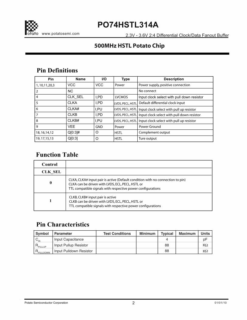
Function Table
Pin Characteristics
Pin Definitions
Input clock select with pull down resistor
LVDS, PECL, HSTL
LVDS, PECL, HSTL
LVDS, PECL, HSTL
LVDS, PECL, HSTL
Input clock select with pull down resistor
Input clock select with pull up resistor
Input clock select with pull up resistor
I,PU
I,PU
GND Power Ground
HSTL
HSTL
CLKA, CLKA# input pair is active (Default condition with no connection to pin)CLKA can be driven with LVDS, ECL, PECL, HSTL or TTL compatible signals with respective power configurations
CLKB, CLKB# input pair is activeCLKB can be driven with LVDS, ECL, PECL, HSTL or TTL compatible signals with respective power configurations
Control
CLK_SEL
0
1
Complement output
Default differential clock input
No connect
Power supply, positive connectionPower
LVCMOS
Ture output
lobmyS retemara sP noitidnoCtse mT uminiM lacipyT mumixaM stinUC NI ecnaticapaCtupnI F4 pR PULLUP rotsiseRpulluPtupnI 88
88KKR NWODLLUP rotsiseRnwodlluPtupnI
VCCVCC
Name I/O Type DescriptionPin
VEE
Q[0:3]#
Q[0:3]
NC
CLK_SEL
CLKA
CLKA#
CLKB
CLKB#
I,PD
I,PD
I,PD
O
O
Power
1, 10,11,20,3
18, 16,14,12
19, 17,15,13
2
4
5
6
7
8
9
2.3V - 3.6V 2:4 Differential Clock/Data Fanout Buffer
2 01/01/10Potato Semiconductor Corporation
PO74HSTL314Awww.potatosemi.com
500MHz HSTL Potato Chip
DC Electrical CharacteristicsSymbol Description Test Conditions Min Typ Max Unit
VOH Output High voltage Vcc=3V Vin=VIH or VIL, IOH= -12mA 2.4 3 - V
VOL Output Low voltage Vcc=3V Vin=VIH or VIL, IOH=12mA - 0.3 0.5 V
VIK Clamp diode voltage Vcc = Min. And IIN = -18mA
Vcc = 0V. Vi or Vo = 0V to 5.5V
- -0.7 -1.2 V
I - - +
Notes:1. For conditions shown as Max. or Min., use appropriate value specified under Electrical Characteristics for the applicable device type.2. Typical values are at Vcc = 3.3V, 25 °C ambient.3. This parameter is guaranteed but not tested.4. Not more than one output should be shorted at one time. Duration of the test should not exceed one second.5. VoH = Vcc – 0.6V at rated current
Maximum Ratings
Description Max Unit
Storage Temperature -65 to 150 °C
Operation Temperature -40 to 85 °C
Operation Voltage -0.5 to +4.6 V
Input Voltage -0.5 to +5.5 V
Output Voltage -0.5 to Vcc+0.5 V
Note:stresses greater than listed underMaximum Ratings may causepermanent damage to the device. Thisis a stress rating only and functionaloperation of the device at these or anyother conditions above those indicatedin the operational sections of thisspecification is not implied. Exposureto absolute maximum rating conditionsfor extended periods may affectreliability specification is not implied.
Multiple Supplies: The Voltage on any input or I/O pin cannot exceed the power pin during power-up. Power supply sequencing is NOT required.
OFFPower off output leakage current uA-5
2.3V - 3.6V 2:4 Differential Clock/Data Fanout Buffer
3 01/01/10Potato Semiconductor Corporation
PO74HSTL314Awww.potatosemi.com
500MHz HSTL Potato Chip

Power Supply CharacteristicsSymbol Description Test Conditions (1) Min Typ Max Unit
IccQ Quiescent Power Supply Current Vcc=Max, Vin=Vcc or GND - 0.1 30 uA
Notes:1. For conditions shown as Max. or Min., use appropriate value specified under Electrical Characteristics for the applicable device type.2. Typical values are at Vcc = 3.3V, 25°C ambient.3. This parameter is guaranteed but not tested.4. Not more than one output should be shorted at one time. Duration of the test should not exceed one second.
Switching CharacteristicstinUxaM)1(snoitidnoCtseTnoitpircseDlobmyS
tPD Propagation Delay CLKA or CLKB to Output pair CL = 15pF 3.2 ns
tr/tf Rise/Fall Time 0.8V – 2.0V 0.8 ns
tsk(p) Pulse Skew (Same Package)
tsk(o) Output Pin to Pin Skew (Same Package)
ps
ps
pstsk(pp) Output Skew (Different Package)
fmax Fp51=LCycneuqerFtupnI 250 MHz
fmax Fp5=LCycneuqerFtupnI 300 MHz
fmax Fp2=LCycneuqerFtupnI 400 MHz
Notes:1. See test circuits and waveforms.2. tpLH, tpHL, tsk(p), and tsk(o) are production tested. All other parameters guaranteed but not production tested.3. Airflow of 1m/s is recommended for frequencies above 133MHz
CL = 15pF, 125MHz
CL = 15pF, 125MHz
CL = 15pF, 125MHz
80
80
350
400
480
500
2.3V - 3.6V 2:4 Differential Clock/Data Fanout Buffer
4 01/01/10Potato Semiconductor Corporation
PO74HSTL314Awww.potatosemi.com
500MHz HSTL Potato Chip

Test Waveforms
VPP RANGE0V-VCC
FIGURE 1. LVDS/ PECL/ ECL/ HSTL /DIFFERENTIAL INPUT WAVEFORM DEFINITIONS
FIGURE 2. HSTL/HSTL OUTPUT
FIGURE 3. Propogation Delay, Output pulse skew, and output-to-output skew for both CLKA or CLKB to output pair
VPP
TPHL
TPLHTPD
INPUTCLOCK
OUTPUTCLOCK
ANOTHEROUTPUTCLOCK
VO
tSK(O)
VCC= 3.3V
VEE=0.0V
VIH
VIL
VPP
VCC
VEE
VOtr,tf,20-80%
2.3V - 3.6V 2:4 Differential Clock/Data Fanout Buffer
5 01/01/10Potato Semiconductor Corporation
PO74HSTL314Awww.potatosemi.com
500MHz HSTL Potato Chip

Packaging Mechanical Drawing: 20 pin SSOP
2.3V - 3.6V 2:4 Differential Clock/Data Fanout Buffer
.272
.295
.078
.002
SEATING PLANE
.0098Max.
.0256 BSC
1
20
.197
.220
0.25X.XXX.XX
DENOTES DIMENSIONSIN MILLIMETERS0.050
5.005.60
2.00
6.907.50
0.65
Max
Min
.022
.037
.004
.009
.291
.3227.408.20
0.550.95
0.090.25
Test Circuit
50Ohm
50Ohm
50pFto
2pF
50pFto
2pF
6 01/01/10Potato Semiconductor Corporation
PO74HSTL314Awww.potatosemi.com
500MHz HSTL Potato Chip
Top-Marking
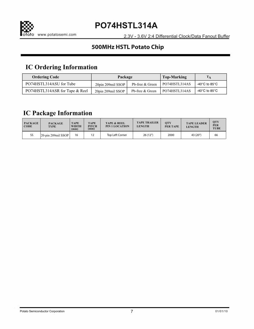
IC Ordering InformationOrdering Code Package
20pin 209mil SSOP Pb-free & Green
PO74HSTL314ASU for Tube
PO74HSTL314ASR for Tape & Reel
PO74HSTL314AS
PO74HSTL314AS
-40°C to 85°C
-40°C to 85°C
TA
2.3V - 3.6V 2:4 Differential Clock/Data Fanout Buffer
7 01/01/10Potato Semiconductor Corporation
PO74HSTL314Awww.potatosemi.com
500MHz HSTL Potato Chip
IC Package InformationPACKAGE
SS 16 12 Top Left Corner 26 (12”) 2000 43 (20”) 6620-pin 209mil SSOP
CODEPACKAGETYPE
TAPEWIDTH
TAPE TRAILER
TUBE
TAPE & REELLENGTH
TAPEPITCH
QTYLENGTHTAPE LEADER
PER TAPE
QTYPERPIN 1 LOCATION
(mm)(mm)
20pin 209mil SSOP Pb-free & Green
Related Documents