Qualcomm Technologies, Inc. For additional information or to submit technical questions, go to https://www.96boards.org/product/dragonboard820c Qualcomm Quick Charge, and TurboCharge are products of Qualcomm Technologies, Inc. Qualcomm WiPower wireless charging technology is licensed by Qualcomm Incorporated. Other Qualcomm products referenced herein are products of Qualcomm Technologies, Inc. or its subsidiaries. DragonBoard, Qualcomm, and WiPower are trademarks of Qualcomm Incorporated, registered in the United States and other countries. Quick Charge is a trademark of Qualcomm Incorporated. TurboCharge is a trademark of Summit Microelectronics, Inc. Other product and brand names may be trademarks or registered trademarks of their respective owners. Use of this document is subject to the license set forth in Exhibit 1. Qualcomm Technologies, Inc. 5775 Morehouse Drive San Diego, CA 92121 U.S.A. © 2014, 2016, 2018 Qualcomm Technologies, Inc. All rights reserved. PMI8994/PMI8996 Power Management IC Device Specification LM80-NT441-15 Rev. C February 16, 2018

Welcome message from author
This document is posted to help you gain knowledge. Please leave a comment to let me know what you think about it! Share it to your friends and learn new things together.
Transcript
Qualcomm Technologies, Inc.
For additional information or to submit technical questions, go to https://www.96boards.org/product/dragonboard820c
Qualcomm Quick Charge, and TurboCharge are products of Qualcomm Technologies, Inc. Qualcomm WiPower wireless charging technology is licensed by Qualcomm Incorporated. Other Qualcomm products referenced herein are products of Qualcomm Technologies, Inc. or its subsidiaries.
DragonBoard, Qualcomm, and WiPower are trademarks of Qualcomm Incorporated, registered in the United States and other countries. Quick Charge is a trademark of Qualcomm Incorporated. TurboCharge is a trademark of Summit Microelectronics, Inc. Other product and brand names may be trademarks or registered trademarks of their respective owners.
Use of this document is subject to the license set forth in Exhibit 1.
Qualcomm Technologies, Inc.5775 Morehouse DriveSan Diego, CA 92121
U.S.A.
© 2014, 2016, 2018 Qualcomm Technologies, Inc. All rights reserved.
PMI8994/PMI8996 Power Management IC
Device Specification
LM80-NT441-15 Rev. C
February 16, 2018

LM80-NT441-15 Rev. C 2
Revision history
Revision Date Description
A December 2014 Initial release
B February 2016 Removed references to QTI.
In Table 3-5, Battery charger specifications, updated footnote 34 on charger switching frequency.
In Table 3-28, UVLO Performance Specification: removed 75mV as Vlowbatt step.
Removed section 6.3 Daisy chain components
Removed Section 6.4 Board-level reliability
C February 2018 Updated the document as per the new branding guidelines
LM80-NT441-15 Rev. C 3
Contents
1 Introduction . . . . . . . . . . . . . . . . . . . . . . . . . . . . . . . . . . . . . . . . . . . . . . . . . . . 81.1 Documentation overview . . . . . . . . . . . . . . . . . . . . . . . . . . . . . . . . . . . . . . . . . . . . . . . . . . . 8
1.2 PMI8994/PMI8996 introduction . . . . . . . . . . . . . . . . . . . . . . . . . . . . . . . . . . . . . . . . . . . . . . 9
1.3 PMI8994/PMI8996 features . . . . . . . . . . . . . . . . . . . . . . . . . . . . . . . . . . . . . . . . . . . . . . . 11
1.3.1 Summary of PMI8994/PMI8996 features . . . . . . . . . . . . . . . . . . . . . . . . . . . . . . 11
1.4 Terms and acronyms . . . . . . . . . . . . . . . . . . . . . . . . . . . . . . . . . . . . . . . . . . . . . . . . . . . . . 15
1.5 Special marks . . . . . . . . . . . . . . . . . . . . . . . . . . . . . . . . . . . . . . . . . . . . . . . . . . . . . . . . . . 17
2 Pad definitions . . . . . . . . . . . . . . . . . . . . . . . . . . . . . . . . . . . . . . . . . . . . . . . . 182.1 I/O parameter definitions . . . . . . . . . . . . . . . . . . . . . . . . . . . . . . . . . . . . . . . . . . . . . . . . . . 20
2.2 Pad descriptions . . . . . . . . . . . . . . . . . . . . . . . . . . . . . . . . . . . . . . . . . . . . . . . . . . . . . . . . 20
3 Electrical specifications . . . . . . . . . . . . . . . . . . . . . . . . . . . . . . . . . . . . . . . . 313.1 Absolute maximum ratings . . . . . . . . . . . . . . . . . . . . . . . . . . . . . . . . . . . . . . . . . . . . . . . . 31
3.2 Operating conditions . . . . . . . . . . . . . . . . . . . . . . . . . . . . . . . . . . . . . . . . . . . . . . . . . . . . . 32
3.3 DC power consumption . . . . . . . . . . . . . . . . . . . . . . . . . . . . . . . . . . . . . . . . . . . . . . . . . . . 33
3.4 Digital logic characteristics . . . . . . . . . . . . . . . . . . . . . . . . . . . . . . . . . . . . . . . . . . . . . . . . 34
3.4.1 Battery charger . . . . . . . . . . . . . . . . . . . . . . . . . . . . . . . . . . . . . . . . . . . . . . . . . 35
3.4.2 Fuel gauge . . . . . . . . . . . . . . . . . . . . . . . . . . . . . . . . . . . . . . . . . . . . . . . . . . . . . 41
3.5 Output power management . . . . . . . . . . . . . . . . . . . . . . . . . . . . . . . . . . . . . . . . . . . . . . . . 51
3.5.1 Boost/bypass SMPS . . . . . . . . . . . . . . . . . . . . . . . . . . . . . . . . . . . . . . . . . . . . . 52
3.5.2 HF-SMPS . . . . . . . . . . . . . . . . . . . . . . . . . . . . . . . . . . . . . . . . . . . . . . . . . . . . . . 54
3.5.3 FT-SMPS . . . . . . . . . . . . . . . . . . . . . . . . . . . . . . . . . . . . . . . . . . . . . . . . . . . . . . 57
3.5.4 +5 V SmartBoost SMPS . . . . . . . . . . . . . . . . . . . . . . . . . . . . . . . . . . . . . . . . . . 60
3.5.5 Reference circuit . . . . . . . . . . . . . . . . . . . . . . . . . . . . . . . . . . . . . . . . . . . . . . . . 62
3.5.6 Internal voltage-regulator connections . . . . . . . . . . . . . . . . . . . . . . . . . . . . . . . . 62
3.6 General housekeeping . . . . . . . . . . . . . . . . . . . . . . . . . . . . . . . . . . . . . . . . . . . . . . . . . . . 63
3.6.1 Analog multiplexer and scaling circuits . . . . . . . . . . . . . . . . . . . . . . . . . . . . . . . 64
3.6.2 HKADC circuit . . . . . . . . . . . . . . . . . . . . . . . . . . . . . . . . . . . . . . . . . . . . . . . . . . 68
3.6.3 Clock input . . . . . . . . . . . . . . . . . . . . . . . . . . . . . . . . . . . . . . . . . . . . . . . . . . . . . 68
3.6.4 Over-temperature protection (smart thermal control) . . . . . . . . . . . . . . . . . . . . 69
3.7 User interfaces . . . . . . . . . . . . . . . . . . . . . . . . . . . . . . . . . . . . . . . . . . . . . . . . . . . . . . . . . 69
3.7.1 Haptics . . . . . . . . . . . . . . . . . . . . . . . . . . . . . . . . . . . . . . . . . . . . . . . . . . . . . . . . 71
3.7.2 Display ± bias . . . . . . . . . . . . . . . . . . . . . . . . . . . . . . . . . . . . . . . . . . . . . . . . . . 72
3.7.3 Flash drivers (including torch mode) . . . . . . . . . . . . . . . . . . . . . . . . . . . . . . . . . 79
3.7.4 White LEDs . . . . . . . . . . . . . . . . . . . . . . . . . . . . . . . . . . . . . . . . . . . . . . . . . . . . 80

LM80-NT441-15 Rev. C 4
PMI8994/PMI8996 Power Management IC Device Specification Contents
3.7.5 Other current sinks and current drivers . . . . . . . . . . . . . . . . . . . . . . . . . . . . . . . 83
3.7.6 Light pulse generators . . . . . . . . . . . . . . . . . . . . . . . . . . . . . . . . . . . . . . . . . . . . 84
3.8 IC-level interfaces . . . . . . . . . . . . . . . . . . . . . . . . . . . . . . . . . . . . . . . . . . . . . . . . . . . . . . . 85
3.8.1 Power-on circuits and power sequences . . . . . . . . . . . . . . . . . . . . . . . . . . . . . . 85
3.8.2 SPMI and the interrupt managers . . . . . . . . . . . . . . . . . . . . . . . . . . . . . . . . . . . 86
3.9 Configurable I/Os . . . . . . . . . . . . . . . . . . . . . . . . . . . . . . . . . . . . . . . . . . . . . . . . . . . . . . . 86
3.9.1 GPIO specifications . . . . . . . . . . . . . . . . . . . . . . . . . . . . . . . . . . . . . . . . . . . . . . 86
3.9.2 MPP specifications . . . . . . . . . . . . . . . . . . . . . . . . . . . . . . . . . . . . . . . . . . . . . . 87
4 Mechanical information . . . . . . . . . . . . . . . . . . . . . . . . . . . . . . . . . . . . . . . . . 894.1 Device physical dimensions . . . . . . . . . . . . . . . . . . . . . . . . . . . . . . . . . . . . . . . . . . . . . . . 89
4.2 Part marking . . . . . . . . . . . . . . . . . . . . . . . . . . . . . . . . . . . . . . . . . . . . . . . . . . . . . . . . . . . 90
4.2.1 Specification-compliant devices . . . . . . . . . . . . . . . . . . . . . . . . . . . . . . . . . . . . . 90
4.3 Device ordering information . . . . . . . . . . . . . . . . . . . . . . . . . . . . . . . . . . . . . . . . . . . . . . . 91
4.3.1 Specification-compliant devices . . . . . . . . . . . . . . . . . . . . . . . . . . . . . . . . . . . . . 91
4.4 Device moisture-sensitivity level . . . . . . . . . . . . . . . . . . . . . . . . . . . . . . . . . . . . . . . . . . . . 91
5 Carrier, storage, and handling information . . . . . . . . . . . . . . . . . . . . . . . . . 935.1 Carrier . . . . . . . . . . . . . . . . . . . . . . . . . . . . . . . . . . . . . . . . . . . . . . . . . . . . . . . . . . . . . . . . 93
5.1.1 Tape and reel information . . . . . . . . . . . . . . . . . . . . . . . . . . . . . . . . . . . . . . . . . 93
5.2 Storage . . . . . . . . . . . . . . . . . . . . . . . . . . . . . . . . . . . . . . . . . . . . . . . . . . . . . . . . . . . . . . . 94
5.2.1 Bagged storage conditions . . . . . . . . . . . . . . . . . . . . . . . . . . . . . . . . . . . . . . . . 94
5.2.2 Out-of-bag duration . . . . . . . . . . . . . . . . . . . . . . . . . . . . . . . . . . . . . . . . . . . . . . 94
5.3 Handling . . . . . . . . . . . . . . . . . . . . . . . . . . . . . . . . . . . . . . . . . . . . . . . . . . . . . . . . . . . . . . 94
5.3.1 Baking . . . . . . . . . . . . . . . . . . . . . . . . . . . . . . . . . . . . . . . . . . . . . . . . . . . . . . . . 94
5.3.2 Electrostatic discharge . . . . . . . . . . . . . . . . . . . . . . . . . . . . . . . . . . . . . . . . . . . . 95
6 PCB mounting guidelines . . . . . . . . . . . . . . . . . . . . . . . . . . . . . . . . . . . . . . . 966.1 RoHS compliance . . . . . . . . . . . . . . . . . . . . . . . . . . . . . . . . . . . . . . . . . . . . . . . . . . . . . . . 96
6.2 SMT parameters . . . . . . . . . . . . . . . . . . . . . . . . . . . . . . . . . . . . . . . . . . . . . . . . . . . . . . . . 96
6.2.1 Land pad and stencil design . . . . . . . . . . . . . . . . . . . . . . . . . . . . . . . . . . . . . . . 96
6.2.2 Reflow profile . . . . . . . . . . . . . . . . . . . . . . . . . . . . . . . . . . . . . . . . . . . . . . . . . . . 98
6.2.3 SMT peak package-body temperature . . . . . . . . . . . . . . . . . . . . . . . . . . . . . . . 98
6.2.4 SMT process verification . . . . . . . . . . . . . . . . . . . . . . . . . . . . . . . . . . . . . . . . . . 99
7 Part reliability . . . . . . . . . . . . . . . . . . . . . . . . . . . . . . . . . . . . . . . . . . . . . . . . 1007.1 Reliability qualifications summary . . . . . . . . . . . . . . . . . . . . . . . . . . . . . . . . . . . . . . . . . . 100
7.2 Qualification sample description . . . . . . . . . . . . . . . . . . . . . . . . . . . . . . . . . . . . . . . . . . . 102

LM80-NT441-15 Rev. C 5
PMI8994/PMI8996 Power Management IC Device Specification
Tables
Table 1-1 Primary PMI8994/PMI8996 device documentation . . . . . . . . . . . . . . . . . . . . . . . . . . . .8Table 1-2 PMI8994/PMI8996 features . . . . . . . . . . . . . . . . . . . . . . . . . . . . . . . . . . . . . . . . . . . . . 11Table 1-3 Terms and acronyms . . . . . . . . . . . . . . . . . . . . . . . . . . . . . . . . . . . . . . . . . . . . . . . . . .15Table 1-4 Special marks . . . . . . . . . . . . . . . . . . . . . . . . . . . . . . . . . . . . . . . . . . . . . . . . . . . . . . . .17Table 2-1 I/O description (pad type) parameters . . . . . . . . . . . . . . . . . . . . . . . . . . . . . . . . . . . . .20Table 2-2 Pad descriptions – input power management functions . . . . . . . . . . . . . . . . . . . . . . .21Table 2-3 Pad descriptions – output power management functions . . . . . . . . . . . . . . . . . . . . . .23Table 2-4 Pad descriptions – general housekeeping functions . . . . . . . . . . . . . . . . . . . . . . . . . .24Table 2-5 Pad descriptions – user interface functions . . . . . . . . . . . . . . . . . . . . . . . . . . . . . . . . .25Table 2-6 Pad descriptions – IC-level interface functions . . . . . . . . . . . . . . . . . . . . . . . . . . . . . .27Table 2-7 Pad descriptions – configurable input/output functions . . . . . . . . . . . . . . . . . . . . . . . .28Table 2-8 Pad descriptions – power supply pads . . . . . . . . . . . . . . . . . . . . . . . . . . . . . . . . . . . .29Table 2-9 Pad descriptions – ground pads . . . . . . . . . . . . . . . . . . . . . . . . . . . . . . . . . . . . . . . . .29Table 3-1 Absolute maximum ratings . . . . . . . . . . . . . . . . . . . . . . . . . . . . . . . . . . . . . . . . . . . . . .31Table 3-2 Operating conditions . . . . . . . . . . . . . . . . . . . . . . . . . . . . . . . . . . . . . . . . . . . . . . . . . .32Table 3-3 DC power supply currents . . . . . . . . . . . . . . . . . . . . . . . . . . . . . . . . . . . . . . . . . . . . . .33Table 3-4 Digital I/O characteristics . . . . . . . . . . . . . . . . . . . . . . . . . . . . . . . . . . . . . . . . . . . . . . .34Table 3-5 Battery charger specifications . . . . . . . . . . . . . . . . . . . . . . . . . . . . . . . . . . . . . . . . . . .35Table 3-6 PMI8994 fuel gauge performance specifications . . . . . . . . . . . . . . . . . . . . . . . . . . . . .41Table 3-7 PMI8996 fuel gauge performance specifications . . . . . . . . . . . . . . . . . . . . . . . . . . . . .46Table 3-8 BSI performance specifications . . . . . . . . . . . . . . . . . . . . . . . . . . . . . . . . . . . . . . . . . .50Table 3-9 Output power management summary . . . . . . . . . . . . . . . . . . . . . . . . . . . . . . . . . . . . .51Table 3-10 Boost/bypass SMPS performance specifications . . . . . . . . . . . . . . . . . . . . . . . . . . .52Table 3-11 HF-SMPS performance specifications . . . . . . . . . . . . . . . . . . . . . . . . . . . . . . . . . . . .54Table 3-12 FT-SMPS performance specifications . . . . . . . . . . . . . . . . . . . . . . . . . . . . . . . . . . . .57Table 3-13 Boost regulator performance specifications . . . . . . . . . . . . . . . . . . . . . . . . . . . . . . . .60Table 3-14 Voltage reference performance specifications . . . . . . . . . . . . . . . . . . . . . . . . . . . . . .62Table 3-15 Internal voltage regulator connections . . . . . . . . . . . . . . . . . . . . . . . . . . . . . . . . . . . .62Table 3-16 Analog multiplexer and scaling functions . . . . . . . . . . . . . . . . . . . . . . . . . . . . . . . . . .64Table 3-17 Analog multiplexer performance specifications . . . . . . . . . . . . . . . . . . . . . . . . . . . . .64Table 3-18 AMUX input to ADC output end-to-end accuracy . . . . . . . . . . . . . . . . . . . . . . . . . . .67Table 3-19 HK/XO ADC performance specifications . . . . . . . . . . . . . . . . . . . . . . . . . . . . . . . . . .68Table 3-20 XO input performance specifications . . . . . . . . . . . . . . . . . . . . . . . . . . . . . . . . . . . . .68Table 3-21 Haptics performance specifications . . . . . . . . . . . . . . . . . . . . . . . . . . . . . . . . . . . . . .71Table 3-22 Display plus bias performance specifications . . . . . . . . . . . . . . . . . . . . . . . . . . . . . .72Table 3-23 Display minus bias performance specifications . . . . . . . . . . . . . . . . . . . . . . . . . . . . .75Table 3-24 Flash and torch LED driver performance specifications . . . . . . . . . . . . . . . . . . . . . .79Table 3-25 WLED boost converter and driver performance specifications . . . . . . . . . . . . . . . . .81Table 3-26 Other current sinks and drivers performance specifications . . . . . . . . . . . . . . . . . . .84Table 3-27 LPG channel assignments and external availability . . . . . . . . . . . . . . . . . . . . . . . . . .84Table 3-28 UVLO performance specifications . . . . . . . . . . . . . . . . . . . . . . . . . . . . . . . . . . . . . . .86Table 3-29 Programmable GPIO configurations . . . . . . . . . . . . . . . . . . . . . . . . . . . . . . . . . . . . .86Table 3-30 Multipurpose pad performance specifications . . . . . . . . . . . . . . . . . . . . . . . . . . . . . .88Table 4-1 PMI8994/PMI8996 device marking line definitions . . . . . . . . . . . . . . . . . . . . . . . . . . .90Table 4-2 Device identification code/ordering information details . . . . . . . . . . . . . . . . . . . . . . . .91Table 4-3 Source configuration code . . . . . . . . . . . . . . . . . . . . . . . . . . . . . . . . . . . . . . . . . . . . . .91Table 4-4 MSL ratings summary . . . . . . . . . . . . . . . . . . . . . . . . . . . . . . . . . . . . . . . . . . . . . . . . .92

LM80-NT441-15 Rev. C 6
PMI8994/PMI8996 Power Management IC Device Specification
Table 6-1 QTI typical SMT reflow profile conditions (for reference only) . . . . . . . . . . . . . . . . . . .98Table 7-1 PMI8994 IC reliability evaluation . . . . . . . . . . . . . . . . . . . . . . . . . . . . . . . . . . . . . . . .100Table 7-2 PMI8996 IC reliability evaluation . . . . . . . . . . . . . . . . . . . . . . . . . . . . . . . . . . . . . . . .101

LM80-NT441-15 Rev. C 7
PMI8994/PMI8996 Power Management IC Device Specification
Figures
Figure 1-1 High-level PMI8994/PMI8996 functional block diagram . . . . . . . . . . . . . . . . . . . . . . .10Figure 2-1 PMI8994/PMI8996 pad assignments (top view) . . . . . . . . . . . . . . . . . . . . . . . . . . . . .19Figure 3-9 PMI8994 SoC accuracy plot for 1.15 A discharging (4.35 V 3 Ah battery), measured on PMI8994 v2.0 . . . . . . . . . . . . . . . . . . . . . . . . . . . . . . . . . . . . . . . . . . . . . . . . . . . . . . . . . . . . . . . .44Figure 3-10 PMI8994 SoC accuracy plot for 1.15 A discharging (4.2 V 1.5 Ah battery), measured on PMI8994 v2.0 . . . . . . . . . . . . . . . . . . . . . . . . . . . . . . . . . . . . . . . . . . . . . . . . . . . . . . . . . . . . . . . .45Figure 3-11 PMI8994 SoC accuracy plot for 1.5 A charging with 5 V DCP (4.35 V 3 Ah battery), measured on PMI8994 v2.0 . . . . . . . . . . . . . . . . . . . . . . . . . . . . . . . . . . . . . . . . . . . . . . . . . . . . . . . . . . . . .46Figure 3-12 Output power management functional block diagram . . . . . . . . . . . . . . . . . . . . . . .51Figure 3-13 Boost/bypass efficiency plot, measured on PMI8994 v2.0 . . . . . . . . . . . . . . . . . . . .54Figure 3-14 S1 efficiency plot, measured on PMI8994 v2.0 . . . . . . . . . . . . . . . . . . . . . . . . . . . .57Figure 3-15 S2/S3 dual-phase efficiency plot, measured on PMI8994 v2.0 . . . . . . . . . . . . . . . .60Figure 3-16 General housekeeping functional block diagram . . . . . . . . . . . . . . . . . . . . . . . . . . .63Figure 3-17 Multiplexer offset and gain errors . . . . . . . . . . . . . . . . . . . . . . . . . . . . . . . . . . . . . . .66Figure 3-18 Analog multiplexer load condition for settling time specification . . . . . . . . . . . . . . .66Figure 3-19 User interface functional block diagram . . . . . . . . . . . . . . . . . . . . . . . . . . . . . . . . . .70Figure 3-20 Display plus bias efficiency plot for LCD mode measured on PMI8994 v2.0 . . . . . .74Figure 3-21 Display plus bias efficiency plot for AMOLED mode measured on PMI8994 v2.0 . .74Figure 3-22 Display minus bias efficiency plot for LCD mode measured on PMI8994 v2.0 . . . .77Figure 3-23 Display minus bias efficiency plot for AMOLED mode (-1.4 V) measured on PMI8994 v2.0 77Figure 3-24 Display minus bias efficiency plot for AMOLED mode (-2.4 V) measured on PMI8994 v2.0 78Figure 3-25 Display minus bias efficiency plot for AMOLED mode (-4.0 V) measured on PMI8994 v2.0 78Figure 3-26 Display minus bias efficiency plot for AMOLED mode (-4.0 V) measured on PMI8994 v2.0 79Figure 3-27 IC-level interfaces functional block diagram . . . . . . . . . . . . . . . . . . . . . . . . . . . . . . .85Figure 4-1 210 WLNSP (5.69 × 6.24 × 0.55 mm) package outline drawing . . . . . . . . . . . . . . . .89Figure 4-2 PMI8994/PMI8996 device marking (top view, not to scale) . . . . . . . . . . . . . . . . . . . .90Figure 4-3 Device identification code . . . . . . . . . . . . . . . . . . . . . . . . . . . . . . . . . . . . . . . . . . . . . .91Figure 5-1 Carrier tape drawing with part orientation . . . . . . . . . . . . . . . . . . . . . . . . . . . . . . . . .93Figure 5-2 Tape handling . . . . . . . . . . . . . . . . . . . . . . . . . . . . . . . . . . . . . . . . . . . . . . . . . . . . . . .94Figure 6-1 Stencil printing aperture area ratio (AR) . . . . . . . . . . . . . . . . . . . . . . . . . . . . . . . . . . .97Figure 6-2 Acceptable solder-paste geometries . . . . . . . . . . . . . . . . . . . . . . . . . . . . . . . . . . . . .97
LM80-NT441-15 Rev. C 8
1 Introduction
This document provides a description of chipset capabilities. Not all features are available, nor are all features supported in the software.
NOTE: Enabling some features may require additional licensing fees.
1.1 Documentation overview
This device specification defines the PMI8994/PMI8996 power management IC (PMIC). Technical information for the PMI8994/PMI8996 is primarily covered by the documents listed in Table 1-1; these documents should be studied for a thorough understanding of the IC and its applications. Released PMI8994/PMI8996 documents are posted at https://discuss.96boards.org/c/products/dragonboard820c and are available for download.
This PMI8994/PMI8996 device specification is organized as follows:
Chapter 1 Provides an overview of PMI8994/PMI8996 documentation, shows a high-level PMI8994/PMI8996 functional block diagram, lists the device features, and lists terms and acronyms used throughout this document.
Chapter 2 Defines the IC pad assignments.
Chapter 3 Defines the IC electrical performance specifications, including absolute maximum ratings and operating conditions.
Chapter 4 Provides IC mechanical information, including dimensions, markings, ordering information, moisture sensitivity, and thermal characteristics.
Chapter 5 Discusses shipping, storage, and handling of PMI8994/PMI8996 devices.
Table 1-1 Primary PMI8994/PMI8996 device documentation
Document number Title/description
LM80-NT411-15
(this document)
PMI8994/PMI8996 Power Management IC Device Specification
This document provides all PMI8994/PMI8996 electrical and mechanical specifications. Additional material includes pad assignment definitions, shipping, storage, and handling instructions, PCB mounting guidelines, and part reliability. This document can be used by company purchasing departments to facilitate procurement.
LM80-NT411-17 PMI8994/PMI8996 Device Revision Guide
This document provides a history of PMI8994 revisions. It explains how to identify the various IC revisions and discusses known issues (or bugs) for each revision and how to work around them.

LM80-NT441-15 Rev. C 9
PMI8994/PMI8996 Power Management IC Device Specification Introduction
Chapter 6 Presents procedures and specifications for mounting the PMI8994/PMI8996 onto printed circuit boards (PCBs).
Chapter 7 Presents PMI8994/PMI8996 reliability data, including definitions of the qualification samples and a summary of qualification test results.
1.2 PMI8994/PMI8996 introduction
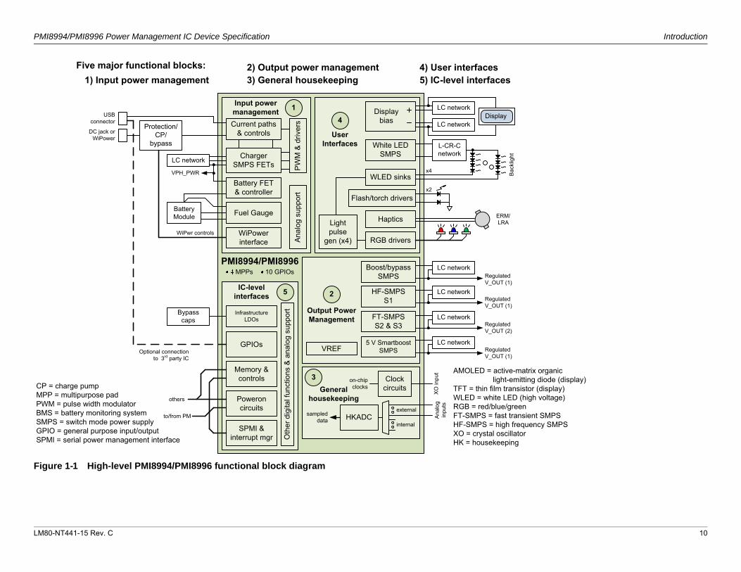
The PMI8994/PMI8996 (Figure 1-1) supplements the PM8994/PM8996 device to integrate all wireless handset power management, general housekeeping, and user interface support functions into a two IC solution. This versatile solution is suitable for multimode, multiband phones, and other wireless products such as data cards and PDAs.
The PMI8994/PMI8996 mixed-signal BiCMOS device is available in the 210-pad wafer-level nanoscale package (210 WLNSP) that includes ground pads for improved electrical ground, mechanical stability, and thermal conductivity.
Since the PMI8994/PMI8996 includes so many diverse functions, its operation is more easily understood by considering major functional blocks individually. Therefore, the PMI8994/PMI8996 document set is organized by the following device functionality:
Input power management
Output power management
General housekeeping
User interfaces
IC interfaces
Configurable pads – either multipurpose pads (MPPs) or general-purpose input/output (GPIOs) – that can be configured to function within some of the other categories
Most information contained in this device specification is organized accordingly – including the circuit groupings within the block diagram (Figure 1-1), pad descriptions (Chapter 2), and detailed electrical specifications (Chapter 3).
PMI8994/PMI8996 Power Management IC Device Specification Introduction
LM80-NT441-15 Rev. C 10
Figure 1-1 High-level PMI8994/PMI8996 functional block diagram
Flash/torch drivers
SPMI & interrupt mgr
Poweron circuits
PMI8994/PMI899610 GPIOs
Input power management
IC-level interfaces
User Interfaces
Output Power Management
Regulated V_OUT (1)
USB connector
DC jack or WiPower
VREF
FT-SMPSS2 & S3
LC network
5 V SmartboostSMPS
General housekeeping
HKADC Ana
log
inpu
ts
Clock circuits
AMOLED = active-matrix organic light-emitting diode (display)
TFT = thin film transistor (display)WLED = white LED (high voltage)RGB = red/blue/greenFT-SMPS = fast transient SMPSHF-SMPS = high frequency SMPSXO = crystal oscillatorHK = housekeeping
Haptics ERM/LRA
3
White LED SMPS
L-CR-C network
WLED sinks Bac
klig
ht
on-chip clocks
Battery Module
PW
M &
driv
ers
1
RGB drivers
4
25
Memory & controls
Current paths & controls
GPIOs
HF-SMPSS1
XO
inpu
t
Display bias
sampled data
internal
external
Oth
er d
igita
l fun
ctio
ns &
ana
log
supp
ort
Optional connection to 3rd party IC
others
to/from PM
LC network
LC network
Regulated V_OUT (2)
Regulated V_OUT (1)
Protection/ CP/
bypass
Charger SMPS FETs
VPH_PWR
LC network
Fuel Gauge
Battery FET & controller
LC network
LC networkDisplay
MPPs
1) Input power management2) Output power management3) General housekeeping
4) User interfaces5) IC-level interfaces
Five major functional blocks:
CP = charge pumpMPP = multipurpose padPWM = pulse width modulatorBMS = battery monitoring systemSMPS = switch mode power supplyGPIO = general purpose input/outputSPMI = serial power management interface
Boost/bypassSMPS
LC networkRegulated V_OUT (1)
Infrastructure LDOs
Bypass caps
Anal
og s
uppo
rt
x4
x2
Light pulse
gen (x4)WiPower interface
WiPwr controls

LM80-NT441-15 Rev. C 11
PMI8994/PMI8996 Power Management IC Device Specification Introduction
1.3 PMI8994/PMI8996 features
NOTE: Some hardware features integrated within the PMI8994/PMI8996 device must be enabled through the IC software.
1.3.1 Summary of PMI8994/PMI8996 features
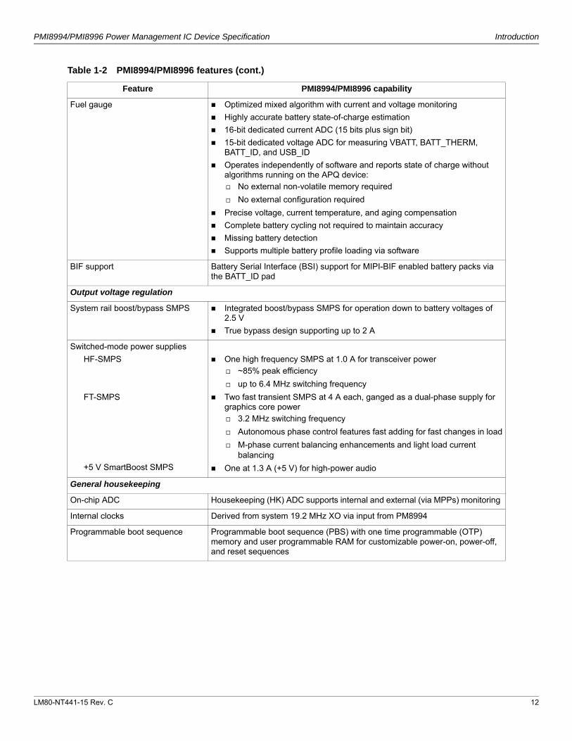
Table 1-2 lists the PMI8994/PMI8996 features.
Table 1-2 PMI8994/PMI8996 features
Feature PMI8994/PMI8996 capability
Input power management
Battery charger Switching charger (SCHG) – switched mode battery charger with reverse boost mode capability
Highly efficient (~93% peak efficiency) power conversion eliminates heat issues
Supports Qualcomm® Quick Charge™ Technology Charge 2.0 for fast charging
Supports parallel charging using SMB1357 companion IC for increased efficiency and lower power dissipation at higher charge currents
High charging current in constant current charging mode, up to 3.0 A
Supports trickle charge, precharge, constant current charging, and constant voltage charging
Two input paths with automatic and programmable input current limit for universal USB/AC/DC adapter compatibility
A4WP Wireless Power (Qualcomm® WiPower™ wireless charging technology) v1.2 support
Automatic power source detection, prioritization, and programmable input current limiting per USB charging specification 1.2 (USB2.0/3.0 compliant)
Up to 750 mA charging output from a 500 mA USB port using TurboCharge™ Mode
Input/output current path control allows system operation with deeply discharged/missing battery
JEITA and JISC 8714 support
Real-time charge and discharge current measurement
+4.0 V to +10 V operating input voltage range
+28 V (USB input), +20 V (DC/WiPower input) input voltage tolerance
(nonoperating) with overvoltage protection (OVP)
USB on-the-go (OTG) support up to 1A (USB OTG standard compliant and USB-IF ACA specification compliant)
Reverse boost support for flash LED current, up to 2.5 A Supports concurrency cases for USB OTG and flash LED
Comprehensive protection features
WiPower support Based upon the A4WP interface specification
IC-level interfacing signals for WiPower ICs such as the Stark DIV2 charge pump IC
LM80-NT441-15 Rev. C 12
PMI8994/PMI8996 Power Management IC Device Specification Introduction
Fuel gauge Optimized mixed algorithm with current and voltage monitoring
Highly accurate battery state-of-charge estimation
16-bit dedicated current ADC (15 bits plus sign bit)
15-bit dedicated voltage ADC for measuring VBATT, BATT_THERM, BATT_ID, and USB_ID
Operates independently of software and reports state of charge without algorithms running on the APQ device: No external non-volatile memory required
No external configuration required
Precise voltage, current temperature, and aging compensation
Complete battery cycling not required to maintain accuracy
Missing battery detection
Supports multiple battery profile loading via software
BIF support Battery Serial Interface (BSI) support for MIPI-BIF enabled battery packs via the BATT_ID pad
Output voltage regulation
System rail boost/bypass SMPS Integrated boost/bypass SMPS for operation down to battery voltages of 2.5 V
True bypass design supporting up to 2 A
Switched-mode power supplies
HF-SMPS
FT-SMPS
+5 V SmartBoost SMPS
One high frequency SMPS at 1.0 A for transceiver power ~85% peak efficiency
up to 6.4 MHz switching frequency
Two fast transient SMPS at 4 A each, ganged as a dual-phase supply for graphics core power 3.2 MHz switching frequency
Autonomous phase control features fast adding for fast changes in load
M-phase current balancing enhancements and light load current balancing
One at 1.3 A (+5 V) for high-power audio
General housekeeping
On-chip ADC Housekeeping (HK) ADC supports internal and external (via MPPs) monitoring
Internal clocks Derived from system 19.2 MHz XO via input from PM8994
Programmable boot sequence Programmable boot sequence (PBS) with one time programmable (OTP) memory and user programmable RAM for customizable power-on, power-off, and reset sequences
Table 1-2 PMI8994/PMI8996 features (cont.)
Feature PMI8994/PMI8996 capability

LM80-NT441-15 Rev. C 13
PMI8994/PMI8996 Power Management IC Device Specification Introduction
User interfaces
Display bias supplies Dual synchronous SMPS topology: Boost and inverting buck-boost
Supports thin film transistor LCD (TFT-LCD) and AMOLED
86% efficiency converters for both rails with compact BOM
2.5 V to 4.6 V input voltage range
Independently programmable positive and negative output voltages
S-Wire interface for programming negative rail
Programmable output voltage: LCD display: +5 V to +6.1 V and -1.4 V to -6.0 V
AMOLED display: +4.6 V to +5 V and -1.4 V to -5.4 V
100 mV resolution on both bias rails
Output voltage accuracy of ±1.7% on negative rail and ±0.8% on positive rail
350 mA output current capability on both supply rails
Auto output disconnect and active discharge on module shutdown
Short circuit protection
Auto power sequencing on module enable/disable
Anti-ringing compensation on both rails
Light load mode for high efficiency
White LED (WLED) backlighting Switched-mode boost supply to adaptively boost voltage for series WLEDs together with four regulated current sinks:
Four LED strings of up to 30 mA each, configurable in 2.5 mA steps
28 V maximum boost voltage
Hybrid dimming mode (analog dimming at high LED currents, digital dimming at low LED currents)
12-bit analog dimming
9-bit digital dimming
Each current sink can be independently controlled via a combination of the brightness control register, full scale current setting register, and an external CABC PWM input.
85% efficiency under typical conditions and 15 mA/string
Light load efficiency mode
High efficiency always on mode
Short circuit detection/protection
Isolation of output from input using an external FET
Fixed voltage regulation mode for AMOLED panels, supports 7.75 V AMOLED reference
Red/green/blue (RGB) LED drivers Three high side current sources for driving LEDs
Independent brightness control of R, G, and B channels.
Supports up to 3 LPG channels for PWM dimming (6 or 9 bits of resolution)
Sources up to 8 mA per channel
Supplied from system-rail boost/bypass for low battery operation
±7% absolute accuracy
300 mV headroom with headroom/dropout detection
Table 1-2 PMI8994/PMI8996 features (cont.)
Feature PMI8994/PMI8996 capability

LM80-NT441-15 Rev. C 14
PMI8994/PMI8996 Power Management IC Device Specification Introduction
Flash drivers Two independent high-side current sources for driving LEDs
Up to 1.0 A per channel
Flexible to support one LED or two LEDs with 2.0 A maximum current
Fully programmable LED currents (0~1.0 A per LED, with 12.5 mA/step)
±8.5% absolute accuracy, ±7% matching accuracy
Current ramp up/down control (programmable ramp rate)
Current mask upon GSM/PA_ON input
Torch mode support at 200 mA per channel
Thermal current derating
Short/open circuit detection
Max-on safety timer, watchdog timer, and thermal shutdown safety
Haptics driver One full H-bridge power stage for driving haptics
Bidirectional drive capability with support for active braking
Support for eccentric rotating machines (ERM)/linear resonant actuators (LRA)
Programmable PWM frequency from 25 kHz to 250 kHz, in 25 kHz steps
Programmable LRA frequency from 50 Hz to 300 Hz, with a 0.5 Hz tuning resolution
6-bit control for output amplitude from 0 V - Vmax, where Vmax is configurable from 1.2 V to 3.6 V, in 100 mV steps for different LRAs
Support for internal 8-bit LUT to store haptics pattern, repeat, and loop
Dual PWM for double the effective switching frequency
Automatic resonance tracking
External input for audio/PWM mode support
Short circuit detection and current limit protection
General-purpose current drivers Two MPPs can function as static current sinks as their alternate functions
Support for up to 40 mA current configurable, in 5 mA steps
±20% accuracy
Light pulse generators Four internally routable PWM generators for a variety of functions
Selectable PWM clock – 1 kHz, 32 kHz, or 19.2 MHz
6, 7, or 9-bit PWM value from lookup table (LUT) or programmed with SPMI
64-element programmable LUT containing the PWM values to be used for pattern generation
Programmable high and low LUT indexes
Programmable up or down index counting
IC-level interfaces
Primary status and control Two-line serial power management interface (MIPI SPMI)
Interrupt managers Supported by SPMI
WiPower support Interfacing signals for WiPower ICs
BUA Battery UICC alarm for graceful shutdown to prevent corruption of UICC on a battery disconnection event
Table 1-2 PMI8994/PMI8996 features (cont.)
Feature PMI8994/PMI8996 capability
LM80-NT441-15 Rev. C 15
PMI8994/PMI8996 Power Management IC Device Specification Introduction
1.4 Terms and acronyms
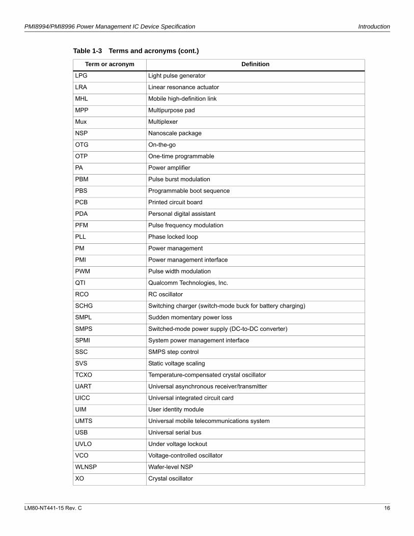
Table 1-3 defines terms and acronyms used throughout this document.
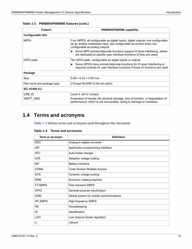
Configurable I/Os
MPPs Four MPPS, all configurable as digital inputs, digital outputs; one configurable as an analog multiplexer input; two configurable as current sinks; two configurable as analog outputs
Some MPP primary/alternate functions support IC-level interfacing, others are dedicated to specific user interface functions (if they are used)
GPIO pads Ten GPIO pads, configurable as digital inputs or outputs
Some GPIOs have primary/alternate functions for IC-level Interfacing or required controls for user interface functions if those UI functions are used
Package
Size 5.69 × 6.24 × 0.55 mm
Pad count and package type 210-pad WLNSP (0.40 mm pitch)
IEC 61000-4-2
USB_ID
VBATT_SNS
Level 4: ±8 kV contact
Evaluation of results: No physical damage, loss of function, or degradation of performance, which is not recoverable, owing to damage to hardware.
Table 1-2 PMI8994/PMI8996 features (cont.)
Feature PMI8994/PMI8996 capability
Table 1-3 Terms and acronyms
Term or acronym Definition
ADC Analog-to-digital converter
API Application programming interface
ATC Auto-trickle charger
AVS Adaptive voltage scaling
BIF Battery interface
CDMA Code Division Multiple Access
DVS Dynamic voltage scaling
ERM Eccentric rotating machine
FT-SMPS Fast transient SMPS
GPIO General-purpose input/output
GSM Global system for mobile communications
HF-SMPS High frequency SMPS
HK Housekeeping
ID Identification
LDO Low dropout (linear regulator)
Li Lithium
LM80-NT441-15 Rev. C 16
PMI8994/PMI8996 Power Management IC Device Specification Introduction
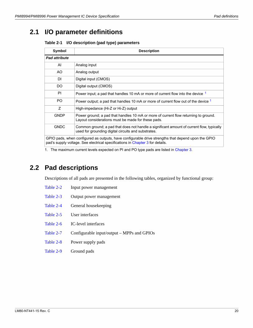
LPG Light pulse generator
LRA Linear resonance actuator
MHL Mobile high-definition link
MPP Multipurpose pad
Mux Multiplexer
NSP Nanoscale package
OTG On-the-go
OTP One-time programmable
PA Power amplifier
PBM Pulse burst modulation
PBS Programmable boot sequence
PCB Printed circuit board
PDA Personal digital assistant
PFM Pulse frequency modulation
PLL Phase locked loop
PM Power management
PMI Power management interface
PWM Pulse width modulation
QTI Qualcomm Technologies, Inc.
RCO RC oscillator
SCHG Switching charger (switch-mode buck for battery charging)
SMPL Sudden momentary power loss
SMPS Switched-mode power supply (DC-to-DC converter)
SPMI System power management interface
SSC SMPS step control
SVS Static voltage scaling
TCXO Temperature-compensated crystal oscillator
UART Universal asynchronous receiver/transmitter
UICC Universal integrated circuit card
UIM User identity module
UMTS Universal mobile telecommunications system
USB Universal serial bus
UVLO Under voltage lockout
VCO Voltage-controlled oscillator
WLNSP Wafer-level NSP
XO Crystal oscillator
Table 1-3 Terms and acronyms (cont.)
Term or acronym Definition

LM80-NT441-15 Rev. C 17
PMI8994/PMI8996 Power Management IC Device Specification Introduction
1.5 Special marks
Special marks used in this document are defined below:
Table 1-4 Special marks
Mark Definition
[ ] Brackets ([ ]) sometimes follow a pad, register, or bit name. These brackets enclose a range of numbers. For example, DATA [7:4] may indicate a range that is 4 bits in length, or DATA[7:0] may refer to eight DATA pads.
_N A suffix of _N indicates an active low signal. For example, PON_RESET_N.
0x0000 Hexadecimal numbers are identified with an x in the number, (for example, 0x0000). All numbers are decimal (base 10) unless otherwise specified. Non-obvious binary numbers have the term binary enclosed in parentheses at the end of the number, [for example, 0011 (binary)].
| A vertical bar in the outside margin of a page indicates that a change was made since the previous revision of this document.

LM80-NT441-15 Rev. C 18
2 Pad definitions
The PMI8994/PMI8996 is available in the 210 WLNSP – see Chapter 4 for package details. A high-level view of the pad assignments is shown in Figure 2-1.

LM80-NT441-15 Rev. C 19
PMI8994/PMI8996 Power Management IC Device Specification Pad definitions
Figure 2-1 PMI8994/PMI8996 pad assignments (top view)
1GND_
BST_BYP
2VREG_
BST_BYP
3VREG_
BST_BYP
4VDD_
S3
5VSW_
S3
6GND_
S3
7GNDC_S2S3
8GNDC_
SUB
9GNDC_S2S3
10GND_
S2
11VSW_
S2
12VDD_
S2
13GNDC_
S1
14VDD_
S1
15VDD_
S1
16GND_
BST_BYP
17VSW_
BST_BYP
18VDD_
BST_BYP
19VDD_
S3
20VSW_
S3
21GND_
S3
22VREF_
NEG_S3
23GNDC_
SUB_S2S3
24VREF_
NEG_S2
25GND_
S2
26VSW_
S2
27VDD_
S2
28GNDC_
S1
29VREG_
S1
30VSW_
S1
31VSW_
BST_BYP
32VSW_
BST_BYP
33FB_
BST_BYP
34MODE_
BST_BYP
35VSW_
S3
36GND_
S3
37VREG_
S3
38HAP_
PWM_IN
39VREG_
S2
40GND_
S2
41VSW_
S2
42VDD_
S2
43
MPP_2
44
MPP_1
45GND_
S1
46VREG_5V_BST
47VREG_5V_BST
48GNDC_
BST
49VDD_HAP
50GND_HAP
51HAP_
OUT_N
52HAP_
OUT_P
53VREG_
ADC_LDO
54AVDD_BYP
55RESIN
_N
56
SHDN_N
57GNDC_
IDSS
58VSNS_FLSH
59VDD_
FLSH_C
60GNDC_FLSH
61VSW_
5V_BST
62VSW_
5V_BST
63GND_
5V_BST
64FB_
5V_BST
65REQ_
5V_BST
66GNDC_
HAP
67
GNDC
68
GPIO_6
69DVDD_BYP
70VDD_
APQ_IO
71PS_
HOLD
72
CLK_IN
73
MPP_3
74VDD_
TORCH
75FLSH_LED1
76VSW_WLED
77WLED_SINK_1
78WLED_SINK_4
79RGB_BLU
80RGB_GRN
81GND_REF
82
BUA
83
GPIO_5
84VDD_
ADC_LDO
85GNDC_
IDSS
86GNDC_
IDSS
87SPMI
_DATA
88
MPP_4
89FLSH_LED1
90VDD_
FLASH
91GND_WLED
92WLED_SINK_2
93WLED_SINK_3
94VDD_RGB
95RGB_RED
96REF_BYP
97GNDC_
MBG
98GNDC_
MBG
99
GNDC
100
GNDC
101GNDC_
CHG
102SPMI_CLK
103GNDC_
SUB
104FLSH_LED2
105FLSH_LED2
106VDD_WLED
107GNDC_DIS_P
108GND_
WLED_I
109CS_
PLUS
110BATT_PLUS
111
GPIO_7
112
GPIO_1
113
GPIO_3
114
GPIO_4
115GNDC_
CHG
116GNDC_
CHG
117GNDC_
CHG
118
DC_IN
119
DC_IN
120
DC_IN
121VREG_WLED
122GND_SUB_DIS_P
123WLED_CABC
124CS_
MINUS
125BATT_MINUS
126
GPIO_8
127
GPIO_2
128GNDC_
CHG
129GNDC_
CHG
130GNDC_
CHG
131USBPHY
_ON
132WIPWR_DIV2_EN
133MID_
DC_IN
134MID_
DC_IN
135MID_
DC_IN
136VDIS_P_OUT
137VSW_DIS_P
138VDIS_P_FB
139
R_BIAS
140VREG_
FG1
141GNDC_
FG
142
GPIO_10
143WIPWR_RST_N
144USB_ID_RVAL1
145STAT_CHG
146
USB_ID
147
SYSON
148DC_IN_OUT
149DC_IN_OUT
150DC_IN_OUT
151GND_DIS_P
152VSW_DIS_P
153VDD_DIS_P
154BATT_THERM
155BATT_ID
156GND_
SUB_FG
157
GPIO_9
158USB_
CS
159EN_CHG
160PGOOD_SYSOK
161VDIR_CHG
162BOOT_CAP
163VSW_CHG
164VSW_CHG
165VSW_CHG
166VDD_DIS_N
167DIS_N_
CAP_REF
168VDIS_N
_FB
169GND_
FG
170GND_
REF_CHG
171USB_
DP
172USB_ID_RVAL2
173
VBATT
174VPH_PWR
175GNDC_
CHG
176VSW_CHG
177VSW_CHG
178MID_
USB_IN
179MID_
USB_IN
180MID_
USB_IN
181VSW_DIS_N
182VSW_DIS_N
183GND_DIS_N_REF
184DIS_
SCTRL
185KYPD_PWR_N
186USB_DM
187VBATT_SNS
188
VBATT
189VPH_PWR
190GNDC_
SUB
191GND_CHG
192GND_CHG
193USB_
IN
194USB_
IN
195USB_
IN
196VDIS_N_OUT
197VDIS_N_OUT
198VDD_1P8_DIS_N
199GNDC_DIS_N
200GND_SUB_DIS_N
201VREG_
FG2
202
VBATT
203
VBATT
204VPH_PWR
205VPH_PWR
206WIPWR_CHG_OK
207GND_CHG
208USB_
IN
209USB_
IN
210USB_
IN
Ground
Input power management
MPPs &GPIOs
IC-level interfaces
Output power management
General housekeeping
User interfaces
LM80-NT441-15 Rev. C 20
PMI8994/PMI8996 Power Management IC Device Specification Pad definitions
2.1 I/O parameter definitions
2.2 Pad descriptions
Descriptions of all pads are presented in the following tables, organized by functional group:
Table 2-2 Input power management
Table 2-3 Output power management
Table 2-4 General housekeeping
Table 2-5 User interfaces
Table 2-6 IC-level interfaces
Table 2-7 Configurable input/output – MPPs and GPIOs
Table 2-8 Power supply pads
Table 2-9 Ground pads
Table 2-1 I/O description (pad type) parameters
Symbol Description
Pad attribute
AI Analog input
AO Analog output
DI Digital input (CMOS)
DO Digital output (CMOS)
PI Power input; a pad that handles 10 mA or more of current flow into the device11
1. The maximum current levels expected on PI and PO type pads are listed in Chapter 3.
PO Power output; a pad that handles 10 mA or more of current flow out of the device 1
Z High-impedance (Hi-Z or Hi-Z) output
GNDP Power ground; a pad that handles 10 mA or more of current flow returning to ground. Layout considerations must be made for these pads.
GNDC Common ground; a pad that does not handle a significant amount of current flow, typically used for grounding digital circuits and substrates.
GPIO pads, when configured as outputs, have configurable drive strengths that depend upon the GPIO pad’s supply voltage. See electrical specifications in Chapter 3 for details.

LM80-NT441-15 Rev. C 21
PMI8994/PMI8996 Power Management IC Device Specification Pad definitions
Table 2-2 Pad descriptions – input power management functions
Pad # Pad name Pad type11 Functional description
Charger/OTG interface
118, 119, 120 DC_IN PI One of two potential charger input power sources that can be connected to the DC jack or WiPower. This is a power entry node for the charger and connects to the OVP circuitry.
193, 194, 195, 208, 209, 210
USB_IN PI, PO One of two potential charger input power sources or output during USB-OTG operation. This is a power entry node for the charger and connects to the OVP circuitry.
186 USB_DM AI USB data minus for power source detection only; data transactions are handled by the APQ device.
171 USB_DP AI/AO USB data plus for power source detection only; data transactions are handled by the APQ device.
146 USB_ID AI OTG mode enable or OTG ID monitor. Input that can be used to either enable OTG mode (this function can also be controlled by the OTG enable bit) or to detect the OTG ID resistor value.
Switching charger (SCHG)
162 BOOT_CAP AO Charger bootstrap node for bootstrapping the charger start-up bias network with input power before starting the SCHG.
133, 134, 135 MID_DC_IN AO Mid-FET capacitor node for accurate current level sensing through OVP FETs of DC_IN; called mid-FET capacitor due to its placement between the OVP FET and the high-side switching FET.
178, 179, 180 MID_USB_IN AO Mid-FET capacitor node for accurate current level sensing through OVP FETs of USB_IN; called mid-FET capacitor due to its placement between the OVP FET and the high-side switching FET.
173, 188, 202, 203
VBATT PI, PO Battery voltage node, connects to BATFET. Output is for charging, and input is for all other operations.
187 VBATT_SNS AI Battery voltage sense input.
161 VDIR_CHG AO, DI Battery charge to discharge the status pad, indicating charge current and charge direction (analog output voltage is proportional to charge current). Can be configured as a digital input to indicate that PA activity is upcoming.
174, 189, 204, 205
VPH_PWR PI, PO Primary system supply node, SCHG regulated node.
148, 149, 150 DC_IN_OUT PO OVP-protected output directly from either DCIN or USBIN. This pad is also the regulated output for the SMBC operating in reverse boost mode to supply USB OTG host mode and/or camera flash.
163, 164, 165, 176, 177
VSW_CHG PI, PO Charger SMPS switching node.
147 SYSON PO Auxiliary supply that provides an OVP-protected 5 V output independent of charging state if the input voltage is valid from a connected charger or OTG voltage generation.
131 USBPHY_ON DO Indicates APSD is complete and the attached device is not an HVDCP; used as a power-on to enable a USB PHY.

LM80-NT441-15 Rev. C 22
PMI8994/PMI8996 Power Management IC Device Specification Pad definitions
191, 192, 207 GND_CHG GNDP Specific ground for the SCHG. Layout considerations must be made for this pad.
170 GND_REF_CHG GNDP Dedicated ground for the charger-specific master bandgap. Special considerations must be made to ensure this ground is properly connected on the PCB.
SCHG digital signals
159 EN_CHG DI Enable input (factory programmable option). Logic high or low (programmable) to enable and/or resume charging. Can be activated by register bit.
145 STAT_CHG DO Status/fault/interrupt indicator. Indicates charging or fault status. Multiplexed static (fault) or pulsed output (IRQ). Programmable polarity.
158 USB_CS DI This is for controlling the default current limit for USB when an SDP is connected and automatic power source detection detects the SDP and is in pad control mode
Fuel gauge/battery interface
125 BATT_MINUS AI Battery minus terminal sense input. Direct connection to the battery (-).
110 BATT_PLUS AI Battery plus terminal sense input. Direct connection to the battery (+).
124 CS_MINUS AI Current sense resistor minus sense input. It connects to the low side of the current sense element.
109 CS_PLUS AI Current sense resistor plus sense input. It connects to the high side of the current sense element.
140 VREG_FG1 AO Bypass capacitor for the internal fuel gauge LDO. It is only used by the fuel gauge and must not be used as a general LDO output.
201 VREG_FG2 AO Bypass capacitor for the internal fuel gauge LDO. It is only used by the fuel gauge and must not be used as a general LDO output.
169 GND_FG GNDP Analog ground for FG. LDO bypass capacitors connect here.
155 BATT_ID AI Battery ID input to ADC and MIPI BIF interface. It can be used for missing battery detection.
154 BATT_THERM AI Battery temperature input to ADC for measuring pack temperature. It is used for charger safe operation and BMS/FG.
139 R_BIAS AO Dedicated voltage source for BAT_THERM resistor network biasing.
Wireless power (WiPower) interface
206 WIPWR_CHG_OK DO Charger request hardware output signal to WiPower. Hi-Z indicates a WiPower charge request. It asserts low to indicate charge done or do not request WiPower charging.
Table 2-2 Pad descriptions – input power management functions (cont.)
Pad # Pad name Pad type11 Functional description

LM80-NT441-15 Rev. C 23
PMI8994/PMI8996 Power Management IC Device Specification Pad definitions
143 WIPWR_RST_N DO Hardware signal that allows PMI to hold the APQ device in reset until power is ready for a dead battery case.
132 WIPWR_DIV2_EN DI Charge pump divide-by-2 indication from the WiPower front end; mode indication to PMI (pass through or divide-by-2) so the appropriate current limit can be selected.
1. See Table 2-1 for parameter and acronym definitions.
Table 2-2 Pad descriptions – input power management functions (cont.)
Pad # Pad name Pad type11 Functional description
Table 2-3 Pad descriptions – output power management functions
Pad # Pad name Pad type11 Functional description
System rail boost/bypass
17, 31, 32 VSW_BST_BYP PO Boost/bypass SMPS switch node.
2, 3 VREG_BST_BYP PO Boost/bypass SMPS regulated output.
33 FB_BST_BYP AI Boost/bypass SMPS feedback node.
34 MODE_BST_BYP DI Boost/bypass SMPS enable input.
18 VDD_BST_BYP PI Boost/bypass SMPS supply power input.
1, 16 GND_BST_BYP GNDP Ground for boost/bypass SMPS circuits.
5 V SmartBoost SMPS circuits
61, 62 VSW_5V_BST PI Boost SMPS switch node.
46, 47 VREG_5V_BST PO Boost SMPS regulated output.
64 FB_5V_BST AI Boost SMPS sense input.
65 REQ_5V_BST DI Hardware signal to request a 5 V boost for audio.
63 GND_5V_BST GNDP Boost SMPS power ground.
High-frequency buck SMPS circuits
30 VSW_S1 PO S1 SMPS switch node.
29 VREG_S1 AI S1 SMPS sense input.
14, 15 VDD_S1 PI S1 SMPS supply power input.
45 GND_S1 GNDP S1 SMPS power ground.
Fast transient buck SMPS circuits
11, 26, 41 VSW_S2 PO S2 SMPS switch node.
39 VREG_S2 AI S2 SMPS sense input.
24 VREF_NEG_S2 AI S2 SMPS ground sense, route as differential pair with VREG_S2.
12, 27, 42 VDD_S2 PI S2 SMPS supply power input.
10, 25, 40 GND_S2 GNDP S2 SMPS power ground.
5, 20, 35 VSW_S3 PO S3 SMPS switch node.
37 VREG_S3 AI S3 SMPS sense input.
22 VREF_NEG_S3 AI S3 SMPS ground sense; route as a differential pair with VREG_S3.
LM80-NT441-15 Rev. C 24
PMI8994/PMI8996 Power Management IC Device Specification Pad definitions
4, 19 VDD_S3 PI S3 SMPS supply power input.
6, 21, 36 GND_S3 GNDP S3 SMPS power ground.
Master bandgap
96 REF_BYP AO Bypass capacitor for dedicated master bandgap regulator. This LDO must only be used for the master bandgap and must not be used as a general LDO output.
81 GND_REF GNDP Dedicated ground for the master bandgap. Special considerations must be made to ensure this ground is properly connected on the PCB.
1. See Table 2-1 for parameter and acronym definitions.
Table 2-3 Pad descriptions – output power management functions (cont.)
Pad # Pad name Pad type11 Functional description
Table 2-4 Pad descriptions – general housekeeping functions
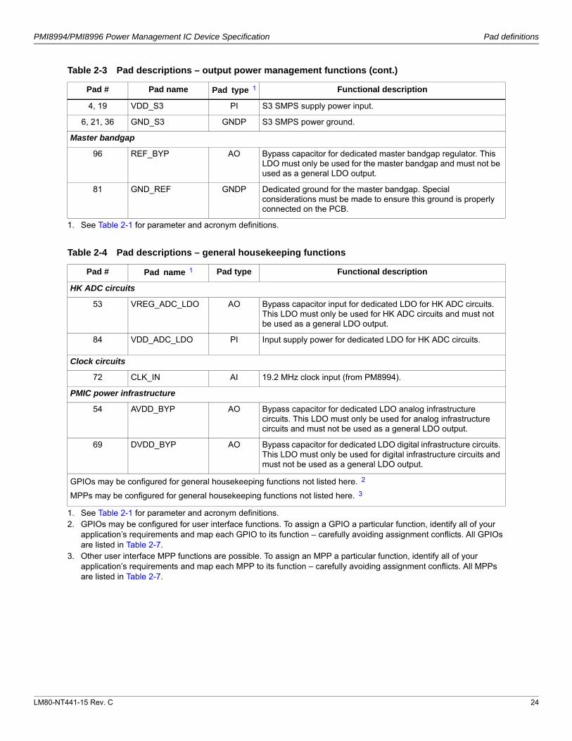
Pad # Pad name11 Pad type Functional description
HK ADC circuits
53 VREG_ADC_LDO AO Bypass capacitor input for dedicated LDO for HK ADC circuits. This LDO must only be used for HK ADC circuits and must not be used as a general LDO output.
84 VDD_ADC_LDO PI Input supply power for dedicated LDO for HK ADC circuits.
Clock circuits
72 CLK_IN AI 19.2 MHz clock input (from PM8994).
PMIC power infrastructure
54 AVDD_BYP AO Bypass capacitor for dedicated LDO analog infrastructure circuits. This LDO must only be used for analog infrastructure circuits and must not be used as a general LDO output.
69 DVDD_BYP AO Bypass capacitor for dedicated LDO digital infrastructure circuits. This LDO must only be used for digital infrastructure circuits and must not be used as a general LDO output.
GPIOs may be configured for general housekeeping functions not listed here.22
MPPs may be configured for general housekeeping functions not listed here.33
1. See Table 2-1 for parameter and acronym definitions.2. GPIOs may be configured for user interface functions. To assign a GPIO a particular function, identify all of your
application’s requirements and map each GPIO to its function – carefully avoiding assignment conflicts. All GPIOs are listed in Table 2-7.
3. Other user interface MPP functions are possible. To assign an MPP a particular function, identify all of your application’s requirements and map each MPP to its function – carefully avoiding assignment conflicts. All MPPs are listed in Table 2-7.
LM80-NT441-15 Rev. C 25
PMI8994/PMI8996 Power Management IC Device Specification Pad definitions
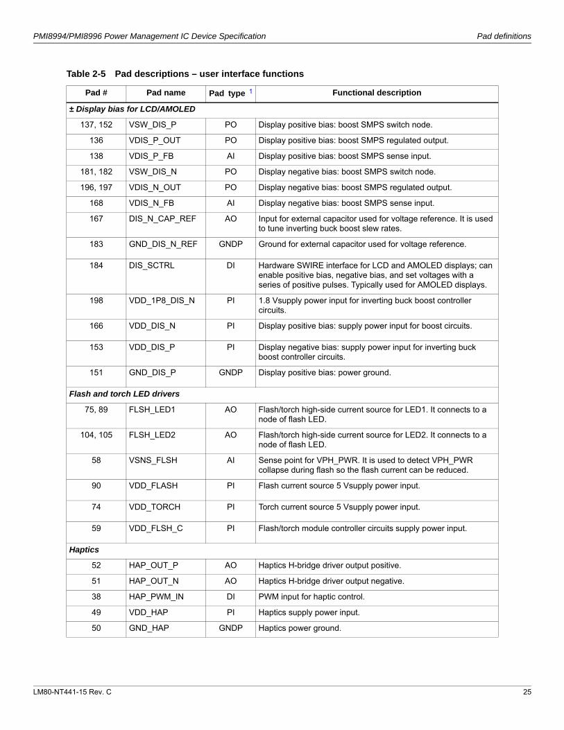
Table 2-5 Pad descriptions – user interface functions
Pad # Pad name Pad type11 Functional description
± Display bias for LCD/AMOLED
137, 152 VSW_DIS_P PO Display positive bias: boost SMPS switch node.
136 VDIS_P_OUT PO Display positive bias: boost SMPS regulated output.
138 VDIS_P_FB AI Display positive bias: boost SMPS sense input.
181, 182 VSW_DIS_N PO Display negative bias: boost SMPS switch node.
196, 197 VDIS_N_OUT PO Display negative bias: boost SMPS regulated output.
168 VDIS_N_FB AI Display negative bias: boost SMPS sense input.
167 DIS_N_CAP_REF AO Input for external capacitor used for voltage reference. It is used to tune inverting buck boost slew rates.
183 GND_DIS_N_REF GNDP Ground for external capacitor used for voltage reference.
184 DIS_SCTRL DI Hardware SWIRE interface for LCD and AMOLED displays; can enable positive bias, negative bias, and set voltages with a series of positive pulses. Typically used for AMOLED displays.
198 VDD_1P8_DIS_N PI 1.8 Vsupply power input for inverting buck boost controller circuits.
166 VDD_DIS_N PI Display positive bias: supply power input for boost circuits.
153 VDD_DIS_P PI Display negative bias: supply power input for inverting buck boost controller circuits.
151 GND_DIS_P GNDP Display positive bias: power ground.
Flash and torch LED drivers
75, 89 FLSH_LED1 AO Flash/torch high-side current source for LED1. It connects to a node of flash LED.
104, 105 FLSH_LED2 AO Flash/torch high-side current source for LED2. It connects to a node of flash LED.
58 VSNS_FLSH AI Sense point for VPH_PWR. It is used to detect VPH_PWR collapse during flash so the flash current can be reduced.
90 VDD_FLASH PI Flash current source 5 Vsupply power input.
74 VDD_TORCH PI Torch current source 5 Vsupply power input.
59 VDD_FLSH_C PI Flash/torch module controller circuits supply power input.
Haptics
52 HAP_OUT_P AO Haptics H-bridge driver output positive.
51 HAP_OUT_N AO Haptics H-bridge driver output negative.
38 HAP_PWM_IN DI PWM input for haptic control.
49 VDD_HAP PI Haptics supply power input.
50 GND_HAP GNDP Haptics power ground.
LM80-NT441-15 Rev. C 26
PMI8994/PMI8996 Power Management IC Device Specification Pad definitions
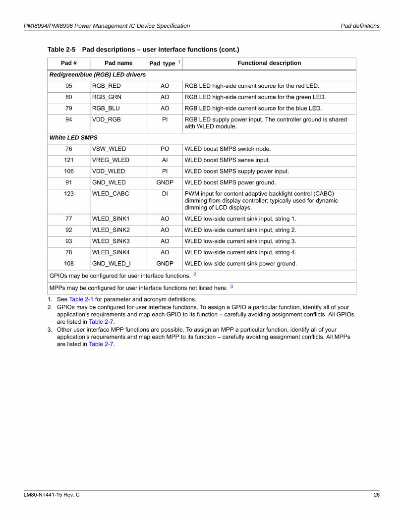
Red/green/blue (RGB) LED drivers
95 RGB_RED AO RGB LED high-side current source for the red LED.
80 RGB_GRN AO RGB LED high-side current source for the green LED.
79 RGB_BLU AO RGB LED high-side current source for the blue LED.
94 VDD_RGB PI RGB LED supply power input. The controller ground is shared with WLED module.
White LED SMPS
76 VSW_WLED PO WLED boost SMPS switch node.
121 VREG_WLED AI WLED boost SMPS sense input.
106 VDD_WLED PI WLED boost SMPS supply power input.
91 GND_WLED GNDP WLED boost SMPS power ground.
123 WLED_CABC DI PWM input for content adaptive backlight control (CABC) dimming from display controller; typically used for dynamic dimming of LCD displays.
77 WLED_SINK1 AO WLED low-side current sink input, string 1.
92 WLED_SINK2 AO WLED low-side current sink input, string 2.
93 WLED_SINK3 AO WLED low-side current sink input, string 3.
78 WLED_SINK4 AO WLED low-side current sink input, string 4.
108 GND_WLED_I GNDP WLED low-side current sink power ground.
GPIOs may be configured for user interface functions.22
MPPs may be configured for user interface functions not listed here.33
1. See Table 2-1 for parameter and acronym definitions.2. GPIOs may be configured for user interface functions. To assign a GPIO a particular function, identify all of your
application’s requirements and map each GPIO to its function – carefully avoiding assignment conflicts. All GPIOs are listed in Table 2-7.
3. Other user interface MPP functions are possible. To assign an MPP a particular function, identify all of your application’s requirements and map each MPP to its function – carefully avoiding assignment conflicts. All MPPs are listed in Table 2-7.
Table 2-5 Pad descriptions – user interface functions (cont.)
Pad # Pad name Pad type11 Functional description
LM80-NT441-15 Rev. C 27
PMI8994/PMI8996 Power Management IC Device Specification Pad definitions
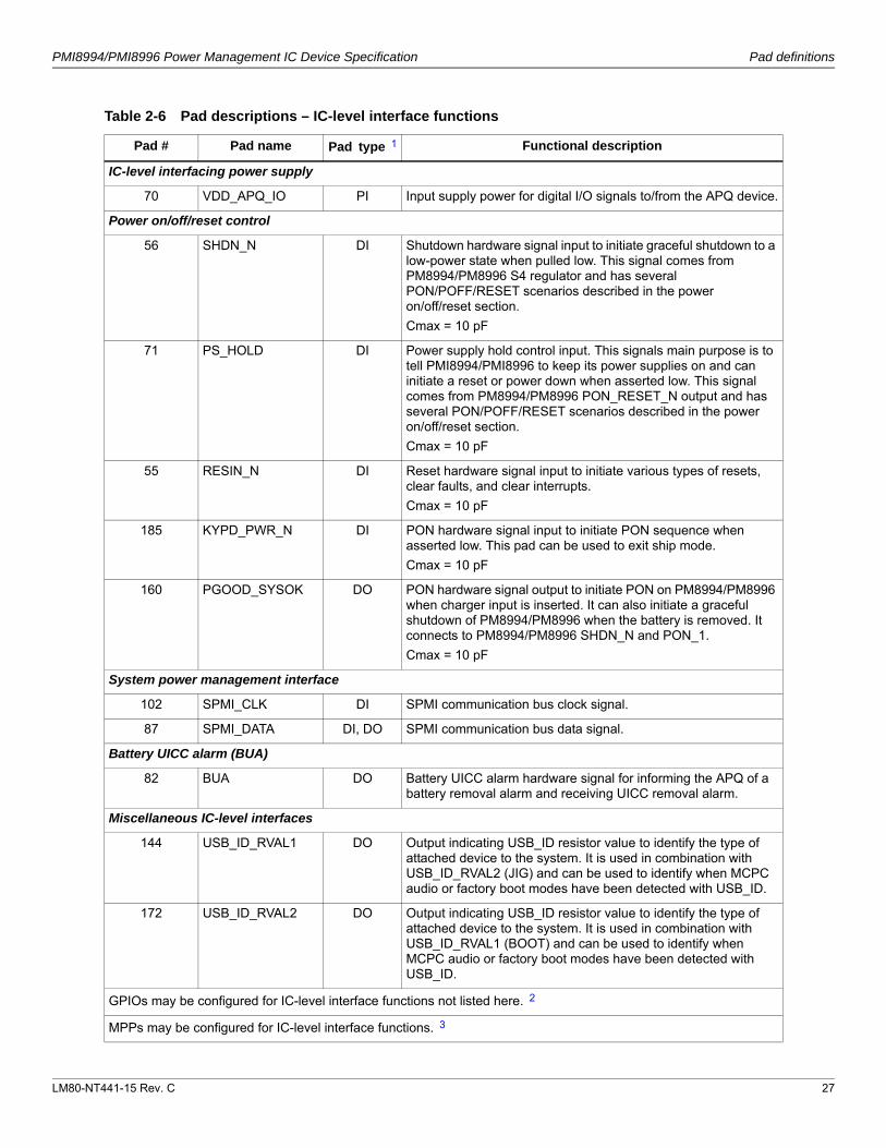
Table 2-6 Pad descriptions – IC-level interface functions
Pad # Pad name Pad type11 Functional description
IC-level interfacing power supply
70 VDD_APQ_IO PI Input supply power for digital I/O signals to/from the APQ device.
Power on/off/reset control
56 SHDN_N DI Shutdown hardware signal input to initiate graceful shutdown to a low-power state when pulled low. This signal comes from PM8994/PM8996 S4 regulator and has several PON/POFF/RESET scenarios described in the power on/off/reset section.
Cmax = 10 pF
71 PS_HOLD DI Power supply hold control input. This signals main purpose is to tell PMI8994/PMI8996 to keep its power supplies on and can initiate a reset or power down when asserted low. This signal comes from PM8994/PM8996 PON_RESET_N output and has several PON/POFF/RESET scenarios described in the power on/off/reset section.
Cmax = 10 pF
55 RESIN_N DI Reset hardware signal input to initiate various types of resets, clear faults, and clear interrupts.
Cmax = 10 pF
185 KYPD_PWR_N DI PON hardware signal input to initiate PON sequence when asserted low. This pad can be used to exit ship mode.
Cmax = 10 pF
160 PGOOD_SYSOK DO PON hardware signal output to initiate PON on PM8994/PM8996 when charger input is inserted. It can also initiate a graceful shutdown of PM8994/PM8996 when the battery is removed. It connects to PM8994/PM8996 SHDN_N and PON_1.
Cmax = 10 pF
System power management interface
102 SPMI_CLK DI SPMI communication bus clock signal.
87 SPMI_DATA DI, DO SPMI communication bus data signal.
Battery UICC alarm (BUA)
82 BUA DO Battery UICC alarm hardware signal for informing the APQ of a battery removal alarm and receiving UICC removal alarm.
Miscellaneous IC-level interfaces
144 USB_ID_RVAL1 DO Output indicating USB_ID resistor value to identify the type of attached device to the system. It is used in combination with USB_ID_RVAL2 (JIG) and can be used to identify when MCPC audio or factory boot modes have been detected with USB_ID.
172 USB_ID_RVAL2 DO Output indicating USB_ID resistor value to identify the type of attached device to the system. It is used in combination with USB_ID_RVAL1 (BOOT) and can be used to identify when MCPC audio or factory boot modes have been detected with USB_ID.
GPIOs may be configured for IC-level interface functions not listed here.22
MPPs may be configured for IC-level interface functions.33

LM80-NT441-15 Rev. C 28
PMI8994/PMI8996 Power Management IC Device Specification Pad definitions
1. See Table 2-1 for parameter and acronym definitions.2. Other IC-level interface GPIO functions are possible. To assign a GPIO a particular function, identify all of your
application’s requirements and map each GPIO to its function – carefully avoiding assignment conflicts. All GPIOs are listed in Table 2-7.
3. MPPs may be configured for IC-level interface functions. To assign an MPP a particular function, identify all of your application’s requirements and map each MPP to its function – carefully avoiding assignment conflicts. All MPPs are listed in Table 2-7.
Table 2-7 Pad descriptions – configurable input/output functions
Pad # Pad name Configurable function Pad type11 Functional description
MPP functions
44 MPP_1 DO-Z Configurable; default Hi-Z output.
WLED_BL_DIM AO Light pulse generators (LPG) PWM used for external WLED backlight dimming.
43 MPP_2 DO-Z Configurable; default Hi output.
FLSH_STROBE DI Digital input for flash strobe signal.
73 MPP_3 DO-Z Configurable; default Hi-Z output.
PMI_SPON DO Interface with PM8994 to continue secondary PON sequence.
TX_GTR_THRESH DI Digital input for transmit greater than threshold to mask flash current.
88 MPP_4 DO-Z Configurable; default Hi-Z output.
EXT_FET_CTL DO Digital output to toggle external FET gate drive. Used for WLED boost short circuit protection.
LED_DRV AO Current sink with four programmable current settings. Can be used to drive a general-purpose LED.
GPIO functions
112 GPIO_1 DI-Z Configurable; default digital input with 10 A pull-down.
127 GPIO_2 DI-Z Configurable; default digital input with 10 A pull-down.
HDMI_EN DO This pad is the digital output to toggle HDMI enable.
113 GPIO_3 DI-Z Configurable; default digital input with 10 A pull-down.
EXT_FET_CTL DO Digital output to toggle external FET gate drive.
114 GPIO_4 DI-Z Configurable; default digital input with 10 A pull-down.
USB2_HS_ID DO Digital output for high-speed USB2 ID.
83 GPIO_5 DI-Z Configurable; default digital input with 10 A pull-down.
USB3_OTG_VBUS_EN DO Digital output to toggle USB3 OTG bus voltage enable.
68 GPIO_6 DI-Z Configurable; default digital input with 10 A pull-down.
USB2_VBUS DI Digital input for USB2 bus voltage detection.
111 GPIO_7 DI-Z Configurable; default digital input with 10 A pull-down.
MASK_2 DI Digital input for optional additional flash mask. See User interfaces: Flash/torch for more details.

LM80-NT441-15 Rev. C 29
PMI8994/PMI8996 Power Management IC Device Specification Pad definitions
NOTE: All GPIOs default to digital input with a 10 A pull-down. All MPPs default to Hi-Z.
NOTE: Configure unused MPPs as 0 mA current sinks (Hi-Z) and GPIOs as digital inputs with their internal pull-downs enabled.
126 GPIO_8 DI-Z Configurable; default digital input with 10 A pull-down.
MASK_3 DI Digital input for optional additional flash mask. See the User interfaces: Flash/torch for more details.
157 GPIO_9 DI-Z Configurable; default digital input with 10 A pull-down.
142 GPIO_10 DI-Z Configurable; default digital input with 10 A pull-down.
1. See Table 2-1 for the parameter and acronym definitions.
Table 2-7 Pad descriptions – configurable input/output functions (cont.)
Pad # Pad name Configurable function Pad type11 Functional description
Table 2-8 Pad descriptions – power supply pads
Power inputs
Note: Power inputs are grouped with their respective module. These can be found in the previous tables.
Table 2-9 Pad descriptions – ground pads
Pad # Pad name Pad type11 Functional description
Common grounds
Note: This table only includes common ground pads. Power ground pads are grouped with their respective modules, and can be found in the previous tables.
101, 115, 116, 117, 128, 129, 130, 175
GNDC_CHG GNDC SMBC controller ground.
190 GNDC_SUB GNDC Substrate ground seal.
141 GNDC_FG GNDC Fuel gauge controller ground.
156 GNDC_SUB_FG GNDC Fuel gauge substrate ground.
48 GNDC_BST GNDC Boost SMPS controller ground.
13, 28 GNDC_S1 GNDC S1 SMPS controller ground.
23 GNDC_SUB_S2S3 GNDC Substrate ground for S2 and S3 power FETs.
7, 9 GNDC_S2S3 GNDC S2, S3 SMPS controller ground.
8 GNDC_SUB GNDC Substrate ground seal.
67, 99, 100 GNDC GNDC Internal common ground.
57, 85, 86 GNDC_IDSS GNDC Ground for digital subsystem circuits.
97, 98 GNDC_MBG GNDC Ground for MBG regulator controller.
107 GNDC_DIS_P GNDC Display bias controller ground.
199 GNDC_DIS_N GNDC Display bias controller ground.

LM80-NT441-15 Rev. C 30
PMI8994/PMI8996 Power Management IC Device Specification Pad definitions
122 GND_SUB_DIS_P GNDC Substrate ground.
200 GND_SUB_DIS_N GNDC Substrate ground.
60 GNDC_FLSH GNDC Flash/torch controller ground.
103 GNDC_SUB GNDC Substrate ground.
66 GNDC_HAP GNDC Haptics controller ground.
1. See Table 2-1 for the parameter and acronym definitions.
Table 2-9 Pad descriptions – ground pads (cont.)
Pad # Pad name Pad type11 Functional description
LM80-NT441-15 Rev. C 31
3 Electrical specifications
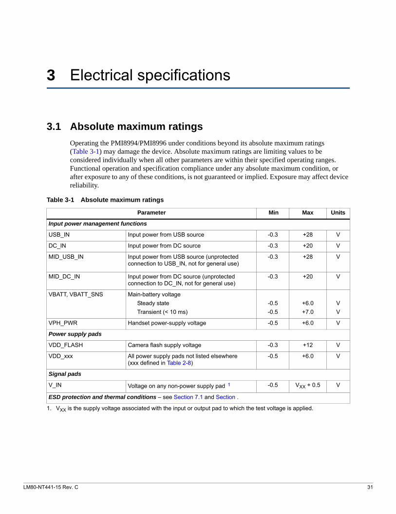
3.1 Absolute maximum ratings
Operating the PMI8994/PMI8996 under conditions beyond its absolute maximum ratings (Table 3-1) may damage the device. Absolute maximum ratings are limiting values to be considered individually when all other parameters are within their specified operating ranges. Functional operation and specification compliance under any absolute maximum condition, or after exposure to any of these conditions, is not guaranteed or implied. Exposure may affect device reliability.
Table 3-1 Absolute maximum ratings
Parameter Min Max Units
Input power management functions
USB_IN Input power from USB source -0.3 +28 V
DC_IN Input power from DC source -0.3 +20 V
MID_USB_IN Input power from USB source (unprotected connection to USB_IN, not for general use)
-0.3 +28 V
MID_DC_IN Input power from DC source (unprotected connection to DC_IN, not for general use)
-0.3 +20 V
VBATT, VBATT_SNS Main-battery voltage
Steady state
Transient (< 10 ms)
-0.5
-0.5
+6.0
+7.0
V
V
VPH_PWR Handset power-supply voltage -0.5 +6.0 V
Power supply pads
VDD_FLASH Camera flash supply voltage -0.3 +12 V
VDD_xxx All power supply pads not listed elsewhere (xxx defined in Table 2-8)
-0.5 +6.0 V
Signal pads
V_IN Voltage on any non-power supply pad11
1. VXX is the supply voltage associated with the input or output pad to which the test voltage is applied.
-0.5 VXX + 0.5 V
ESD protection and thermal conditions – see Section 7.1 and Section .
LM80-NT441-15 Rev. C 32
PMI8994/PMI8996 Power Management IC Device Specification Electrical specifications
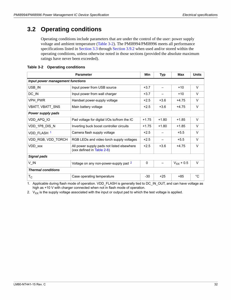
3.2 Operating conditions
Operating conditions include parameters that are under the control of the user: power supply voltage and ambient temperature (Table 3-2). The PMI8994/PMI8996 meets all performance specifications listed in Section 3.3 through Section 3.9.2 when used and/or stored within the operating conditions, unless otherwise noted in those sections (provided the absolute maximum ratings have never been exceeded).
Table 3-2 Operating conditions
Parameter Min Typ Max Units
Input power management functions
USB_IN Input power from USB source +3.7 – +10 V
DC_IN Input power from wall charger +3.7 – +10 V
VPH_PWR Handset power-supply voltage +2.5 +3.6 +4.75 V
VBATT, VBATT_SNS Main battery voltage +2.5 +3.6 +4.75 V
Power supply pads
VDD_APQ_IO Pad voltage for digital I/Os to/from the IC +1.75 +1.80 +1.85 V
VDD_1P8_DIS_N Inverting buck boost controller circuits +1.75 +1.80 +1.85 V
VDD_FLASH11
1. Applicable during flash mode of operation. VDD_FLASH is generally tied to DC_IN_OUT, and can have voltage as high as +10 V with charger connected when not in flash mode of operation.
Camera flash supply voltage +2.5 – +5.5 V
VDD_RGB, VDD_TORCH RGB LEDs and video torch supply voltages +2.5 – +5.5 V
VDD_xxx All power supply pads not listed elsewhere (xxx defined in Table 2-8)
+2.5 +3.6 +4.75 V
Signal pads
V_IN Voltage on any non-power-supply pad22
2. VXX is the supply voltage associated with the input or output pad to which the test voltage is applied.
0 – VXX + 0.5 V
Thermal conditions
TC Case operating temperature -30 +25 +85 °C
LM80-NT441-15 Rev. C 33
PMI8994/PMI8996 Power Management IC Device Specification Electrical specifications
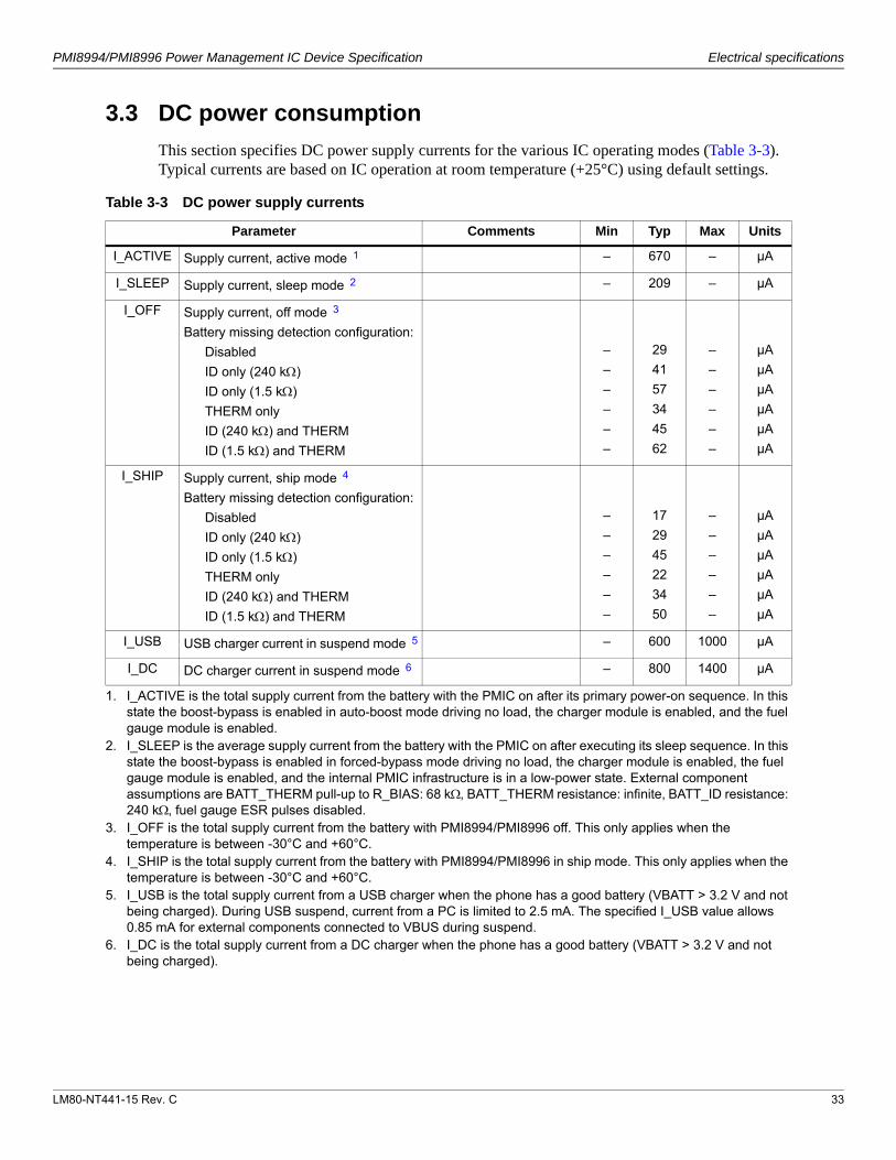
3.3 DC power consumption
This section specifies DC power supply currents for the various IC operating modes (Table 3-3). Typical currents are based on IC operation at room temperature (+25°C) using default settings.
Table 3-3 DC power supply currents
Parameter Comments Min Typ Max Units
I_ACTIVE Supply current, active mode11
1. I_ACTIVE is the total supply current from the battery with the PMIC on after its primary power-on sequence. In this state the boost-bypass is enabled in auto-boost mode driving no load, the charger module is enabled, and the fuel gauge module is enabled.
– 670 – µA
I_SLEEP Supply current, sleep mode22
2. I_SLEEP is the average supply current from the battery with the PMIC on after executing its sleep sequence. In this state the boost-bypass is enabled in forced-bypass mode driving no load, the charger module is enabled, the fuel gauge module is enabled, and the internal PMIC infrastructure is in a low-power state. External component assumptions are BATT_THERM pull-up to R_BIAS: 68 k, BATT_THERM resistance: infinite, BATT_ID resistance: 240 k, fuel gauge ESR pulses disabled.
– 209 – µA
I_OFF Supply current, off mode33
Battery missing detection configuration:
Disabled
ID only (240 k)
ID only (1.5 k)
THERM only
ID (240 k) and THERM
ID (1.5 k) and THERM
3. I_OFF is the total supply current from the battery with PMI8994/PMI8996 off. This only applies when the temperature is between -30°C and +60°C.
–
–
–
–
–
–
29
41
57
34
45
62
–
–
–
–
–
–
µA
µA
µA
µA
µA
µA
I_SHIP Supply current, ship mode44
Battery missing detection configuration:
Disabled
ID only (240 k)
ID only (1.5 k)
THERM only
ID (240 k) and THERM
ID (1.5 k) and THERM
4. I_SHIP is the total supply current from the battery with PMI8994/PMI8996 in ship mode. This only applies when the temperature is between -30°C and +60°C.
–
–
–
–
–
–
17
29
45
22
34
50
–
–
–
–
–
–
µA
µA
µA
µA
µA
µA
I_USB USB charger current in suspend mode55
5. I_USB is the total supply current from a USB charger when the phone has a good battery (VBATT > 3.2 V and not being charged). During USB suspend, current from a PC is limited to 2.5 mA. The specified I_USB value allows 0.85 mA for external components connected to VBUS during suspend.
– 600 1000 µA
I_DC DC charger current in suspend mode66
6. I_DC is the total supply current from a DC charger when the phone has a good battery (VBATT > 3.2 V and not being charged).
– 800 1400 µA

LM80-NT441-15 Rev. C 34
PMI8994/PMI8996 Power Management IC Device Specification Electrical specifications
3.4 Digital logic characteristics
The charger has unique digital signaling characteristics as listed within Section 3.4.2; all other PMI8994/PMI8996 digital I/O characteristics are specified in Table 3-4.
Table 3-4 Digital I/O characteristics
Parameter Comments11
1. VIO is the supply voltage for the PMIC interface (most PMIC digital I/Os).
Min Typ Max Units
VIH High-level input voltage 0.65 · VIO – VIO + 0.3 V
VIL Low-level input voltage -0.3 – 0.35 · VIO V
VSHYS Schmitt hysteresis voltage 15 – – mV
IL Input leakage current22
2. MPP and GPIO pads comply with the input leakage specification only when configured as a digital input or set to the tri-state mode.
VIO = max, VIN = 0 V to VIO -0.20 – +0.20 µA
VOH High-level output voltage Iout = IOH VIO - 0.45 – VIO V
VOL Low-level output voltage Iout = IOL 0 – 0.45 V
IOH High-level output current33
3. Output current specifications apply to all digital outputs unless specified otherwise, and are superseded by specifications for specific pads (such as MPP and GPIO pads).
Vout = VOH 3 – – mA
IOL Low-level output current 3 Vout = VOL – – -3 mA
CIN Input capacitance44
4. Input capacitance is guaranteed by design, but is not 100% tested.
– – 5 pF
LM80-NT441-15 Rev. C 35
PMI8994/PMI8996 Power Management IC Device Specification Electrical specifications
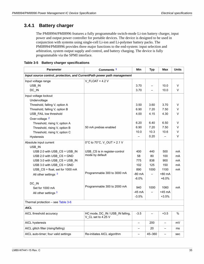
3.4.1 Battery charger
The PMI8994/PMI8996 features a fully programmable switch-mode Li-ion battery charger, input power and output power controller for portable devices. The device is designed to be used in conjunction with systems using single-cell Li-ion and Li-polymer battery packs. The PMI8994/PMI8996 provides three major functions to the end-system: input selection and arbitration, system output supply and control, and battery charging. The device is fully programmable via the SPMI interface.
Table 3-5 Battery charger specifications
Parameter Comments11 Min Typ Max Units
Input source control, protection, and CurrentPath power path management
Input voltage range
USB_IN
DC_IN
V_FLOAT = 4.2 V
3.70
3.70
–
–
10.0
10.0
V
V
Input voltage lockout
Undervoltage
Threshold, falling V, option A
Threshold, falling V, option B
USB_FAIL low threshold
Over-voltage22
Threshold, rising V, option A
Threshold, rising V, option B
Threshold, rising V, option C
Hysteresis
50 mA prebias enabled
3.50
6.90
4.00
6.20
6.90
10.0
–
3.60
7.20
4.15
6.40
7.20
10.3
0.20
3.70
7.50
4.30
6.50
7.50
10.6
–
V
V
V
V
V
V
V
Absolute input current
USB_IN
USB 2.0 with USB_CS = USB_IN
USB 2.0 with USB_CS = GND
USB 3.0 with USB_CS = USB_IN
USB 3.0 with USB_CS = GND
USB_CS = float, set for 1000 mA
All other settings33
DC_IN
Set for 1000 mA
All other settings 3
0°C to 70°C, V_OUT > 2.1 V
USB_CS is in register-control mode by default
Programmable 300 to 3000 mA
Programmable 300 to 2000 mA
400
58
775
102
890
-80 mA
-6.0%
940
-45 mA
-3.5%
440
80
838
125
1000
–
1000
–
500
100
900
150
1100
+80 mA
+6.0%
1060
+45 mA
+3.5%
mA
mA
mA
mA
mA
mA
Thermal protection – see Table 3-6
AICL
AICL threshold accuracy HC mode, DC_IN / USB_IN falling, V_CL set to 4.25 V
-3.5 – +3.5 %
AICL hysteresis – 200 – mV
AICL glitch filter (rising/falling) – 20 – ms
AICL auto-timer; four valid settings Re-initiates AICL algorithm – 45–360 – sec

LM80-NT441-15 Rev. C 36
PMI8994/PMI8996 Power Management IC Device Specification Electrical specifications
APSD44
D+ source voltage (Vdp_src) Current = 125 µA 0.5 0.6 0.7 V
Data detect voltage (Vdata_ref) 0.250 0.325 0.400 V
D+ pull-up voltage (Vdp_up) 3.0 – 3.6 V
D- sink current (Idm_sink) 50 – 150 µA
Data contact detect current source (Idp_src) 7 – 13 µA
Timing characteristics
D+ source on time (tdp_src_on)
D+ source off to high current (tspsrc_hicrnt)
D+ source off to connect (tdpsrc_on)
DCD timeout (tdcd_timeout), option 1
DCD timeout (tdcd_timeout), option 2
Charger detect debounce (chgr_det_dbnc)
100
40
40
321
642
10
–
–
–
328
656
–
–
–
–
335
670
–
ms
ms
ms
ms
ms
ms
D+/D- capacitance (Cdp_dm) APSD completed; D+/D- are Hi-Z – 4 – pF
WiPower
Input impedance limiter ±1 divided by input current limit accuracy
-3.85 – 4.17 %
Input power limiter Maximum power drawn from PMI; smartphone setting
– – 5 W
DC_IN voltage comparator
Threshold
Hysteresis
DIV2_EN = high –
–
6.5
320
–
–
V
mV
DIV2_EN falling-edge deglitch timer Four programmable settings; DIV2_EN high-to-low; AICL disabled-to-enabled
0 – 500 µs
Battery charging with switching charger (SCHG)
Float voltage (V_FLT) range & nominal 20 mV steps 3.60 4.20 4.50 V
Float voltage accuracy
V_FLT ≥ 4.2 V
V_FLT < 4.2 V
T = 0°C to 70°C
–
–
–
–
±0.5
±1.0
%
%
Fast charge current accuracy
1000 mA
All other settings 3
T = 0°C to 70°C
Programmable 300–3000 mA in 32 steps
890-100 mA
-2.5%
1000 1110+100 mA
+2.5%
mA
Charge termination current accuracy55
100 mA
All other settings 3
T = 0°C to 70°C
Programmable 50–600 mA in 8 steps
–
–
–
–
±50
±20
mA
%
Charge termination glitch filter – 1 – sec
Table 3-5 Battery charger specifications (cont.)
Parameter Comments11 Min Typ Max Units

LM80-NT441-15 Rev. C 37
PMI8994/PMI8996 Power Management IC Device Specification Electrical specifications
Recharge threshold voltage66
(V_FLT - VBAT)PMI8994
PMI8996
–
–
200
100 or 150
–
–
mV
mV
Precharge to fast charge threshold accuracy
VBAT rising; 2.8 V setting
Programmable 2.4–3.0 V in 4 steps
– – ±4 %
Precharge current accuracy
100 mA
All other settings 3
T = 0°C to 70°C
Programmable 100–550 mA in 5 steps
–
–
–
–
±20
±20
mA
mA
Trickle to precharge voltage threshold 2.0 2.1 2.2 V
Trickle charge current VBAT = 1.7 V – 45 – mA
Charger buck regulator
Peak switching current USB_IN or DC_IN = 9.0 V – 4.5 – A
Maximum DC output current USB_IN or DC_IN = 9.0 V – 4.0 – A
Switching frequency77 PMI8994
PMI8996
1.92
–
2
750
2.08
–
MHz
kHz
Duty cycle
Maximum
Minimum
–
–
99.3
0
–
–
%
%
Regulated output voltage (VPH)
Charging, VPH_MIN < VPH < VPH_MAX
Not charging, VBAT > VPH_MIN option A
Not charging, VBAT > VPH_MIN option B
VPH = VPH_PWR
–
–
–
VBAT + IR
VBAT + 0.1
VBAT + 0.2
–
–
–
V
V
Maximum regulated output voltage Charging disabled – 4.6 – V
Minimum regulated output voltage
Charging
Three programmable settings for PMI8994
Four programmable settings for PMI8996
–
–
–
–
–
–
–
3.15
3.45
3.60
3.2
3.4
3.6
3.8
–
–
–
–
–
–
–
V
V
V
V
V
V
V
Regulated output voltage accuracy
VPH = 3.6 V, I_SYS = 0 A
VPH = 4.3 V, I_SYS = 0 A
–
–
±1.0
±1.0
±2.5
±2.5
%
%
Output voltage load regulation Load steps from 0 to 1 A in 15 microseconds
VBAT - 0.2
VBAT - 0.1
– V
Table 3-5 Battery charger specifications (cont.)
Parameter Comments11 Min Typ Max Units

LM80-NT441-15 Rev. C 38
PMI8994/PMI8996 Power Management IC Device Specification Electrical specifications
BATFET regulation voltage when an ideal diode
Ideal diode; V_OUT falling, VBAT > V_OUT, I_OUT = 300 mA
– VBAT - 0.050
VBAT - 0.075
V
Efficiency
USB_IN
Peak, 5 V input
Peak, 9 V input
3 A charge current, 9 V input
DC_IN
Peak, 5 V input
Peak, 7 V input
Peak, 9 V input
1.5 A charge current, 5 V input
1.5 A charge current, 7 V input
1.5 A charge current, 9 V input
USB_IN charging efficiency of PMI8996.
–
–
–
–
–
–
–
–
–
92.3
89.1
85.1
91.4
89.9
88.6
87.3
88.7
88.2
–
–
–
–
–
–
–
–
–
%
%
%
%
%
%
%
%
%
Power dissipation
USB_IN
3 A charge current, 9 V input
DC_IN
1.5 A charge current, 5 V input
1.5 A charge current, 7 V input
1.5 A charge current, 9 V input
USB_IN charging power dissipation of PMI8996.
–
–
–
–
2032
849
887
882
–
–
–
–
mW
mW
mW
mW
SYSON analog output
SYSON output voltage For PMI8994, I_OUT = 50 mA;USB_IN or DC_IN > 5.0 V
4.7 5.0 5.3 V
For PMI8996, I_OUT = 50 mA;USB_IN or DC_IN > 5.5 V
5.17 5.5 5.83 V
Battery FET
Battery FET on resistance – 10 16 m
Battery FET continuous current 3 Pad limited – – 6 A
Battery FET peak current 3 Pad limited, 10% duty cycle – – 8 A
USB-OTG, HDMI, MHL modes
OTG output voltage 4.75 5.00 5.25 V
Efficiency See Table 3-6 for typical OTG efficiency curve
– – – %
OTG battery UVLO accuracy, VBAT falling 2.70 to 3.30 V settings – – ±4 %
OTG-specific UVLO hysteresis T = 0°C to 70°C – 50 – mV
OTG-specific standby current See “Current consumption” in Table 3-5
– – – mA
Protection
VBAT overvoltage lockout VBAT rising – V_FLT + 0.1
– V
Table 3-5 Battery charger specifications (cont.)
Parameter Comments11 Min Typ Max Units
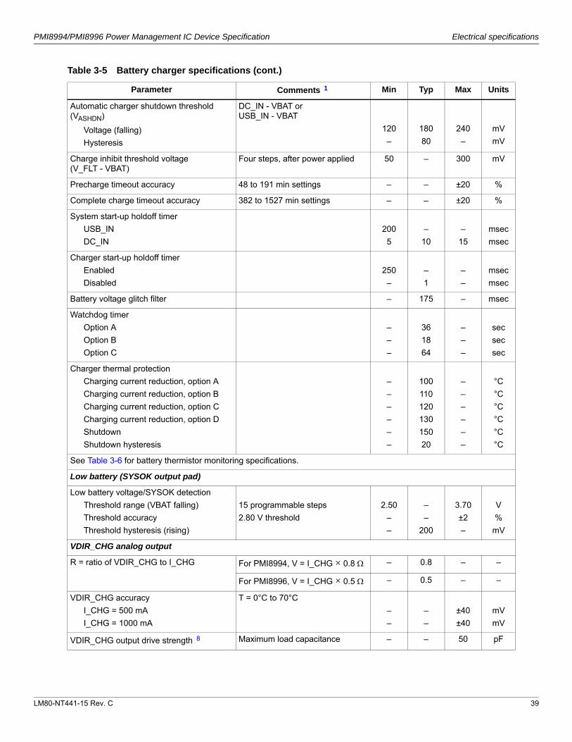
LM80-NT441-15 Rev. C 39
PMI8994/PMI8996 Power Management IC Device Specification Electrical specifications
Automatic charger shutdown threshold (VASHDN)
Voltage (falling)
Hysteresis
DC_IN - VBAT or USB_IN - VBAT
120
–
180
80
240
–
mV
mV
Charge inhibit threshold voltage (V_FLT - VBAT)
Four steps, after power applied 50 – 300 mV
Precharge timeout accuracy 48 to 191 min settings – – ±20 %
Complete charge timeout accuracy 382 to 1527 min settings – – ±20 %
System start-up holdoff timer
USB_IN
DC_IN
200
5
–
10
–
15
msec
msec
Charger start-up holdoff timer
Enabled
Disabled
250
–
–
1
–
–
msec
msec
Battery voltage glitch filter – 175 – msec
Watchdog timer
Option A
Option B
Option C
–
–
–
36
18
64
–
–
–
sec
sec
sec
Charger thermal protection
Charging current reduction, option A
Charging current reduction, option B
Charging current reduction, option C
Charging current reduction, option D
Shutdown
Shutdown hysteresis
–
–
–
–
–
–
100
110
120
130
150
20
–
–
–
–
–
–
°C
°C
°C
°C
°C
°C
See Table 3-6 for battery thermistor monitoring specifications.
Low battery (SYSOK output pad)
Low battery voltage/SYSOK detection
Threshold range (VBAT falling)
Threshold accuracy
Threshold hysteresis (rising)
15 programmable steps
2.80 V threshold
2.50
–
–
–
–
200
3.70
±2
–
V
%
mV
VDIR_CHG analog output
R = ratio of VDIR_CHG to I_CHG For PMI8994, V = I_CHG × 0.8 – 0.8 – –
For PMI8996, V = I_CHG × 0.5 – 0.5 – –
VDIR_CHG accuracy
I_CHG = 500 mA
I_CHG = 1000 mA
T = 0°C to 70°C
–
–
–
–
±40
±40
mV
mV
VDIR_CHG output drive strength88 Maximum load capacitance – – 50 pF
Table 3-5 Battery charger specifications (cont.)
Parameter Comments11 Min Typ Max Units

LM80-NT441-15 Rev. C 40
PMI8994/PMI8996 Power Management IC Device Specification Electrical specifications
Charger-specific digital I/O characteristics (different from general characteristics given in Section 3.4)
High-level input voltage (VIH) Charger digital interface pads: CHG_EN, WIPWR_DIV2_EN, WIPWR_CHG_OK, USB_CS
1.4 – – V
Low-level input voltage (VIL) – – 0.6 V
EN high-level input voltage (VIH) 1.2 – – V
EN low-level input voltage (VIL) – – 0.4 V
Output low-level (VOL), 3 mA sink STAT_CHG, PGOOD_SYSOK – – 0.3 V
RPULL (push-pull configuration) PGOOD_SYSOKVDD = 1.8 V
USBPHY_ON
VDD = 5.0 V
–
–
1.27
1.27
–
–
k
k
Current consumption
ILEAK
EN_CHG, USB_CS
STAT_CHG
V_IN = 3.3 V
V_IN = 5.0 V
–
–
–
–
1.0
1.0
µA
µA
Ground current
Standby (battery)
Shutdown (battery)
Suspend (DC_IN)99
Suspend (USB_IN)
Active
PFM mode, no load
PWM mode, no load 3
OTG-specific standby current
Input present, SHDN = H, USB_IN/DC_IN = 0 V
No input, SHDN = L
No load, PFM mode
No load, PWM mode
–
–
–
–
45
12
2
15
3
27
70
20
5
24
–
–
µA
µA
mA
mA
mA
mA
1. T = -30ºC to +85°C, DC_IN or USB_IN = 5.0 V, V_FLT = 4.2 V, and VBAT = 3.7 V unless otherwise noted.2. Overvoltage lockout depends on the allowed input adapter type selection.3. Not 100% production tested. Guaranteed by design and/or characterization.4. Refer to the USB battery charging specifications 1.1 and 1.2.5. Charge termination current sensed by charger analog sensor. By using a fuel gauge ADC, PMI8996 can achieve a
higher charge termination current accuracy. 6. Battery recharging can also be handled by fuel gauge, based on the battery SoC.7. Although the PMI8994 oscillator frequency can be programmed to 3 MHz, only 2 MHz is supported. For PMI8996, the
default switching frequency of 750 kHz is trimmed 10% lower to achieve better charger efficiency.8. Drive strength/load capacitance is guaranteed by design, but is not 100% tested.9. See Table 3-3 for USB_IN and DC_IN suspend current consumption.
Table 3-5 Battery charger specifications (cont.)
Parameter Comments11 Min Typ Max Units
LM80-NT441-15 Rev. C 41
PMI8994/PMI8996 Power Management IC Device Specification Electrical specifications
3.4.2 Fuel gauge
The fuel gauge module offers a hardware-based algorithm that is able to accurately estimate the battery’s state of charge by using current monitoring and voltage-based techniques. This hybrid approach ensures both excellent short-term linearity and long-term accuracy. Furthermore, neither full battery charge cycling, nor zero-current-load conditions, are required to maintain the accuracy.
The fuel gauge measures the battery pack temperature by sensing the voltage across an external thermistor. Missing battery detection is also incorporated to accurately monitor battery insertion and removal scenarios, while properly updating the state of charge when a battery is reconnected.
Using precise measurements of battery voltage, current, and temperature, the fuel gauging algorithm compensates for the variation in battery characteristics across temperature changes and aging effects. This provides a dependable state of charge estimate throughout the entire life of the battery and across a broad range of operating conditions.
A low level of interaction with the system is required. A broad range of configuration registers are provided to fit the requirements various applications.
Performance specifications for PMI8994 and PMI8996 fuel gauge are presented in Table 3-6 and Table 3-7, respectively.
Table 3-6 PMI8994 fuel gauge performance specifications
Parameter Comments11 Min Typ Max Unit
State of charge accuracy See Figure 3-9 and Figure 3-10 for typical SoC accuracy curves.
– – – %
Voltage ADC – battery voltage conversion
ADC resolution – – 15 bits
LSB magnitude – 152.6 – µV
Conversion time 15 bits – 163.84 – ms
Input voltage range 2.8 – 4.6 V
Gain error
T = 25°C
T = 0°C to +70°C
VBATT = 3.4 to 4.4 V
–
–
±0.2
±0.3
–
–
%
%
Input referred offset error
T = 0°C to +70°C
VBATT = 3.4 to 4.4 V
-2.5 – +2.5 mV
Voltage ADC – thermistor voltage conversion
ADC resolution – 12 – bits
LSB magnitude – 659 – µV
Conversion time 1.47 – 392 s
Input voltage range % of R_BIAS 0 – 90.5 %
Gain error
T = -20°C to +70°C
VBATT_THERM > 1 V, R_BIAS = 2.7 V
-0.6 – +0.6 %
Input referred offset error
T = -20°C to +70°C
VBATT_THERM ≤ 1 V, R_BIAS = 2.7 V
-6 – 6 mV
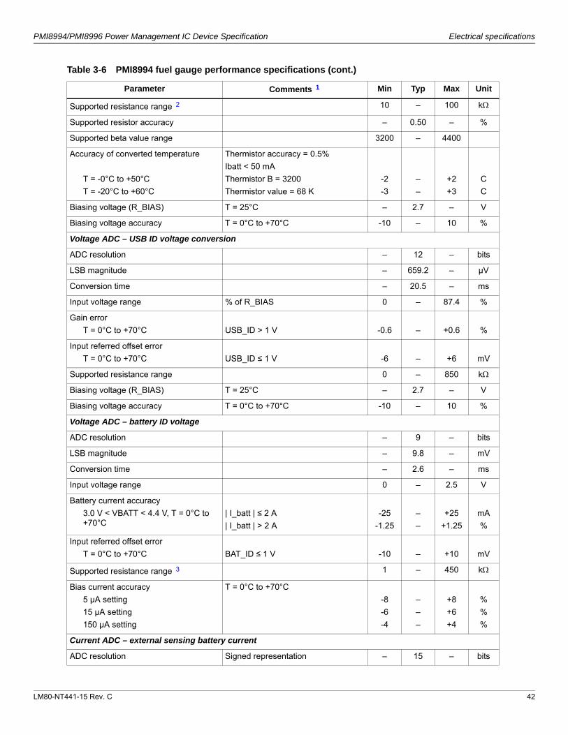
LM80-NT441-15 Rev. C 42
PMI8994/PMI8996 Power Management IC Device Specification Electrical specifications
Supported resistance range22 10 – 100 k
Supported resistor accuracy – 0.50 – %
Supported beta value range 3200 – 4400
Accuracy of converted temperature
T = -0°C to +50°C
T = -20°C to +60°C
Thermistor accuracy = 0.5%
Ibatt < 50 mA
Thermistor B = 3200
Thermistor value = 68 K
-2
-3
–
–
+2
+3
C
C
Biasing voltage (R_BIAS) T = 25°C – 2.7 – V
Biasing voltage accuracy T = 0°C to +70°C -10 – 10 %
Voltage ADC – USB ID voltage conversion
ADC resolution – 12 – bits
LSB magnitude – 659.2 – µV
Conversion time – 20.5 – ms
Input voltage range % of R_BIAS 0 – 87.4 %
Gain error
T = 0°C to +70°C USB_ID > 1 V -0.6 – +0.6 %
Input referred offset error
T = 0°C to +70°C USB_ID ≤ 1 V -6 – +6 mV
Supported resistance range 0 – 850 k
Biasing voltage (R_BIAS) T = 25°C – 2.7 – V
Biasing voltage accuracy T = 0°C to +70°C -10 – 10 %
Voltage ADC – battery ID voltage
ADC resolution – 9 – bits
LSB magnitude – 9.8 – mV
Conversion time – 2.6 – ms
Input voltage range 0 – 2.5 V
Battery current accuracy
3.0 V < VBATT < 4.4 V, T = 0°C to +70°C
| I_batt | ≤ 2 A
| I_batt | > 2 A
-25
-1.25
–
–
+25
+1.25
mA
%
Input referred offset error
T = 0°C to +70°C BAT_ID ≤ 1 V -10 – +10 mV
Supported resistance range33 1 – 450 k
Bias current accuracy
5 µA setting
15 µA setting
150 µA setting
T = 0°C to +70°C
-8
-6
-4
–
–
–
+8
+6
+4
%
%
%
Current ADC – external sensing battery current
ADC resolution Signed representation – 15 – bits
Table 3-6 PMI8994 fuel gauge performance specifications (cont.)
Parameter Comments11 Min Typ Max Unit

LM80-NT441-15 Rev. C 43
PMI8994/PMI8996 Power Management IC Device Specification Electrical specifications
LSB magnitude – 1.5 – µV
Conversion time – 163 – ms
Gain error
T = 25°C
T = 0°C to +70°C
VBATT = 3.0 to 4.4 V
-1
-1.25
–
–
+1
+1.25
%
%
Supported resistance range – 10 – m
Supported resistor accuracy 1 0.5 – %
Converted battery current LSB – 152.6 – µA
Converted battery current range -4.8 – +4.8 A
Input referred offset error T = 0°C to +70°C, VBATT = 3.0 to 4.4 V -25 – +25 mA
Current ADC – internal sensing battery current
ADC resolution Signed representation – 15 – bits
LSB magnitude – 1.5 – µV
Conversion time – 163 – ms
Battery current accuracy
VBATT > 3.6 V, T = 0°C to +70°C | I_batt | ≤ 1 A, input absent
| I_batt | > 1 A, input absent
| I_batt | ≤ 1 A, 5 V/9 V input present, charging disabled
| I_batt | > 1 A, 5 V/9 V input present, charging disabled
| I_batt | ≤ 1 A, 5 V/9 V input present, charging enabled
| I_batt | > 1 A, 5 V/9 V input present, charging enabled
-70
-7
-100
-8
-100
-10
–
–
–
–
–
–
+10
+3
+70
+9
+150
+5
mA
%
mA
%
mA
%
Converted battery current LSB – 152.6 – µA
Converted battery current range -4 – +4 A
ADC shared parameters
ADC clock conversion frequency – 200 – kHz
ADC clock conversion frequency accuracy
T = 0°C to +70°C 193 200 205 kHz
Current consumption
Ground current
Active
Sleep
Fuel gauge is converting voltage/current
BCL in LPM state
–
10
1000
140
–
–
µA
µA
1. T = -30°C to +85°C, +2.7 V < VBATT < +4.5 V unless otherwise noted. All voltages are relative to GND.2. It is not recommended to place any capacitance on the BATT_THERM pad. Capacitance greater than 40 nF with a
10 k nominal thermistor resistance may result in error in the converted temperature exceeding the specification limits.
Table 3-6 PMI8994 fuel gauge performance specifications (cont.)
Parameter Comments11 Min Typ Max Unit

LM80-NT441-15 Rev. C 44
PMI8994/PMI8996 Power Management IC Device Specification Electrical specifications
Figure 3-9 PMI8994 SoC accuracy plot for 1.15 A discharging (4.35 V 3 Ah battery), measured on PMI8994 v2.0
3. It is not recommended to place any capacitance on the BATT_ID pad. Adding capacitance may result in error in the converted battery ID exceeding the specification if the following capacitances are exceeded:
BATT_ID = 1 k to 15 k: 10 nFBATT_ID = 19 k to 140 k: 4.7 nFBATT_ID = 240 k to 450 k: 0.47 nF
0%
10%
20%
30%
40%
50%
60%
70%
80%
90%
100%
10%
8%
6%
4%
2%
0%
2%
4%
6%
8%
10%
0 1000 2000 3000 4000 5000 6000 7000 8000Ba
tterySoC(%
)
SoCerror(%)
Time (s)
SoC accuracy: 1.15A discharging 4.35V 3Ah batteryat 25°C (external current sensing)
SoC Error
Battery SoC
Reference SoC

LM80-NT441-15 Rev. C 45
PMI8994/PMI8996 Power Management IC Device Specification Electrical specifications
Figure 3-10 PMI8994 SoC accuracy plot for 1.15 A discharging (4.2 V 1.5 Ah battery), measured on PMI8994 v2.0
0%
10%
20%
30%
40%
50%
60%
70%
80%
90%
100%
10%
8%
6%
4%
2%
0%
2%
4%
6%
8%
10%
0 500 1000 1500 2000 2500 3000 3500 4000
BatterySoC(%
)
S0Cerror(%)
Time (s)
SoC accuracy: 1.15A discharging 4.2V 1.5Ah batteryat 25°C (external current sensing)
SoC Error
Battery SoC
Reference SoC
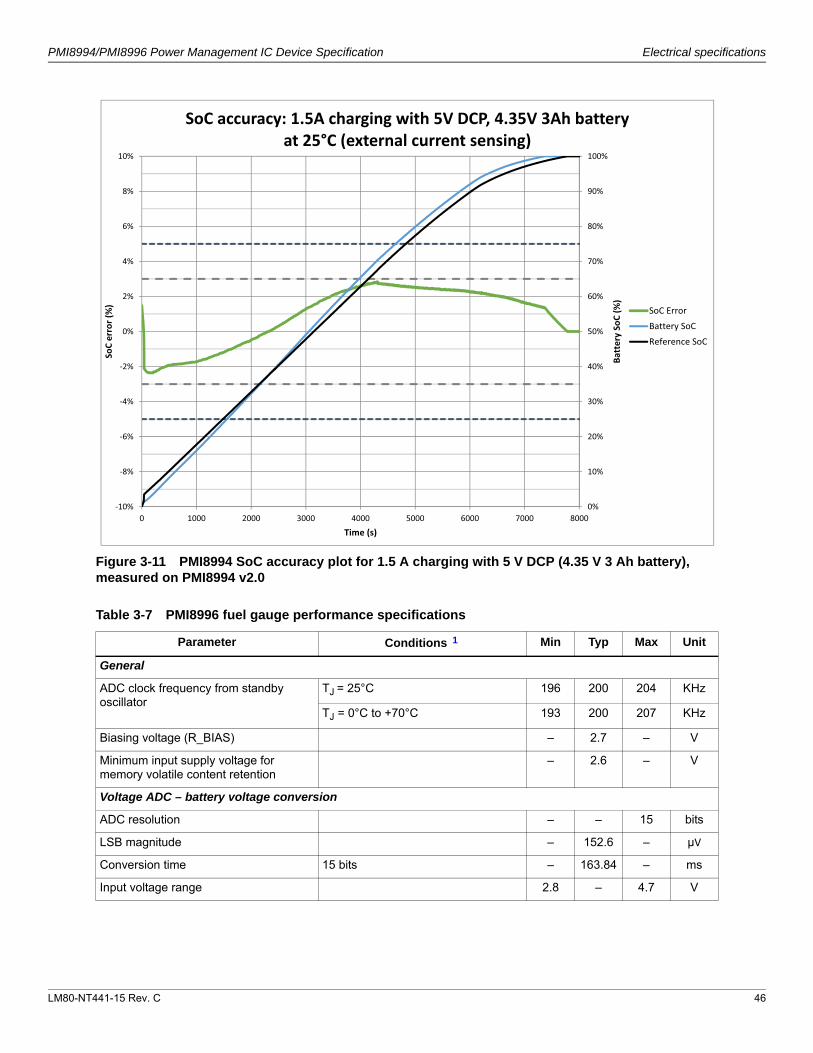
LM80-NT441-15 Rev. C 46
PMI8994/PMI8996 Power Management IC Device Specification Electrical specifications
Figure 3-11 PMI8994 SoC accuracy plot for 1.5 A charging with 5 V DCP (4.35 V 3 Ah battery), measured on PMI8994 v2.0
Table 3-7 PMI8996 fuel gauge performance specifications
Parameter Conditions11 Min Typ Max Unit
General
ADC clock frequency from standby oscillator
TJ = 25°C 196 200 204 KHz
TJ = 0°C to +70°C 193 200 207 KHz
Biasing voltage (R_BIAS) ‒ 2.7 ‒ V
Minimum input supply voltage for memory volatile content retention
‒ 2.6 ‒ V
Voltage ADC – battery voltage conversion
ADC resolution ‒ ‒ 15 bits
LSB magnitude ‒ 152.6 ‒ µV
Conversion time 15 bits ‒ 163.84 ‒ ms
Input voltage range 2.8 ‒ 4.7 V
0%
10%
20%
30%
40%
50%
60%
70%
80%
90%
100%
10%
8%
6%
4%
2%
0%
2%
4%
6%
8%
10%
0 1000 2000 3000 4000 5000 6000 7000 8000
BatterySoC(%
)
SoCerror(%)
Time (s)
SoC accuracy: 1.5A charging with 5V DCP, 4.35V 3Ah batteryat 25°C (external current sensing)
SoC ErrorBattery SoCReference SoC

LM80-NT441-15 Rev. C 47
PMI8994/PMI8996 Power Management IC Device Specification Electrical specifications
Battery voltage absolute accuracy, (PLUSBATT - MINUSBATT)
T = 25°C
VBATT = 3.8 V
No input connected
-0.15 ‒ +0.15 %
T = 0°C to +70°C
VBATT = 3.8 V
No input connected
-0.2 ‒ +0.2 %
T = 25°C
VBATT = 3.8 V
5 V USB Input
-0.25 ‒ +0.25 %
T = 0°C to +70°C
VBATT = 3.8 V
5 V USB Input
-0.3 ‒ +0.3 %
Voltage ADC – thermistor voltage conversion
Thermistor voltage resolution Programmable 9 ‒ 12 bits
Thermistor voltage input range % of R_BIAS 0 ‒ 91.2 %
Thermistor voltage LSB VR_BIAS = 2.7 V 659 ‒ 5273 µV
Thermistor voltage absolute accuracy T =-20°C to +70°CVR_BIAS = 2.7 V
VBAT_THERM > 1 V
-0.8 ‒ +0.8 %
T =-20°C to +70°CVR_BIAS = 2.7 V
VBAT_THERM < 1 V
-8 ‒ 8 mV
Supported thermistor value range 10 ‒ 100 kΩ
Supported thermistor accuracy ‒ 0.50 ‒ %
Supported thermistor beta value range 3200 ‒ 4400
Supported thermistor capacitor value BAT_ThermRES = 10 k ‒ 5 150 nF
Battery temperature measurement accuracy
T = -0°C to +50°C
Thermistor accuracy = 0.5% IBATT < 50 mA
Thermistor B = 3200
Thermistor value= 68 K
-2 ‒ +2 C
T = -20°C to +60°C
Thermistor accuracy = 0.5% IBATT < 50 mA
Thermistor B = 3200
Thermistor value = 68 K
-3 ‒ +3 C
Time between updates 1.47 ‒ 392 s
Biasing voltage (R_BIAS) T = 25°C
During ADC conversion
‒ 2.7 ‒ V
Table 3-7 PMI8996 fuel gauge performance specifications (cont.)
Parameter Conditions11 Min Typ Max Unit

LM80-NT441-15 Rev. C 48
PMI8994/PMI8996 Power Management IC Device Specification Electrical specifications
Biasing voltage accuracy T = 0°C to +70°C
During ADC conversion
-10 ‒ 10 %
Voltage ADC – battery ID voltage
ADC reading resolution ‒ 9 ‒ bits
LSB magnitude ‒ 9.8 ‒ mV
Conversion time ‒ 2.6 ‒ ms
Input voltage range 0 ‒ 2.5 V
Gain error T = 0°C to +70°C
BATT_ID > 1 V
-1 ±0.75 +1 %
Input referred offset error T = 0°C to +70°C
BATTT_ID 1 V
-10 ‒ +10 mV
Current ADC – external sensing battery current
ADC reading resolution Signed representation ‒ 15 ‒ bits
LSB magnitude ‒ 1.5 ‒ µV
Conversion time ‒ 163 ‒ ms
Battery current accuracy T = 0°C to +70°C
VBATT = 3.0 to 4.4 V
IBATT < -1 A (charge)
IBATT > 1 A (discharge)
-1.5 ‒ +1.5 %
T =0oC to +70oC
VBATT = 3.0 to 4.4 V
| IBATT | < 1 A
-15 ‒ +15 mA
Termination current accuracy T = 0°C to +70°C
VBATT = 4.4 V
IBATT = -0.3 A
-15 ‒ +15 mA
Supported resistance range ‒ 10 ‒ mΩ
Supported resistor accuracy ‒ 0.5 1 %
Converted battery current LSB 10 mΩ Rsense ‒ 152.6 ‒ µA
Converted battery current range 10 mΩ Rsense -5.0 ‒ +5.0 A
Current ADC – internal sensing battery current
ADC reading resolution Signed representation ‒ 15 ‒ bits
Battery current accuracy T = 0°C to +70°C
VBATT = 3.4 to 4.4 V
VSYS_MIN = 3.0 V
| IBATT | > 1 A
-7 ‒ +7 %
T = 0°C to +70°C
VBATT = 3.4 to 4.4 V
VSYS_MIN = 3.0 V
| IBATT | < 1 A
-70 ‒ +70 mA
Table 3-7 PMI8996 fuel gauge performance specifications (cont.)
Parameter Conditions11 Min Typ Max Unit

LM80-NT441-15 Rev. C 49
PMI8994/PMI8996 Power Management IC Device Specification Electrical specifications
Termination current accuracy T = 0°C to +70°C
VBATT = 4.4 V
IBATT = -0.3 A
-40 ‒ +40 mA
Converted battery current LSB ‒ 152.6 ‒ µA
Converted battery current range -5.0 ‒ +5.0 A
Conversion time 15 bits ‒ 163 ‒ ms
Current consumption
Ground current
Active
Sleep
Sleep
Fuel gauge is converting voltage/current
Estimated average sleep current
Rock bottom sleep current
‒
‒
10
1000
30
‒
‒
‒
‒
µA
µA
µA
1. T = -10°C to +70°C, +2.7 V < VBATT < +4.5 V, unless otherwise noted. All voltages are relative to GND.
Table 3-7 PMI8996 fuel gauge performance specifications (cont.)
Parameter Conditions11 Min Typ Max Unit
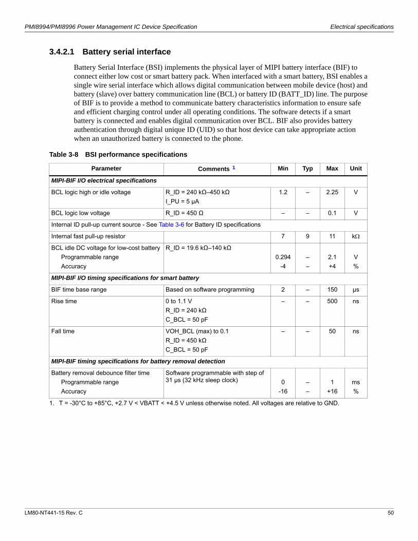
LM80-NT441-15 Rev. C 50
PMI8994/PMI8996 Power Management IC Device Specification Electrical specifications
3.4.2.1 Battery serial interface
Battery Serial Interface (BSI) implements the physical layer of MIPI battery interface (BIF) to connect either low cost or smart battery pack. When interfaced with a smart battery, BSI enables a single wire serial interface which allows digital communication between mobile device (host) and battery (slave) over battery communication line (BCL) or battery ID (BATT_ID) line. The purpose of BIF is to provide a method to communicate battery characteristics information to ensure safe and efficient charging control under all operating conditions. The software detects if a smart battery is connected and enables digital communication over BCL. BIF also provides battery authentication through digital unique ID (UID) so that host device can take appropriate action when an unauthorized battery is connected to the phone.
Table 3-8 BSI performance specifications
Parameter Comments11 Min Typ Max Unit
MIPI-BIF I/O electrical specifications
BCL logic high or idle voltage R_ID = 240 kΩ–450 kΩ
I_PU = 5 µA
1.2 – 2.25 V
BCL logic low voltage R_ID = 450 Ω – – 0.1 V
Internal ID pull-up current source - See Table 3-6 for Battery ID specifications
Internal fast pull-up resistor 7 9 11 k
BCL idle DC voltage for low-cost battery
Programmable range
Accuracy
R_ID = 19.6 kΩ–140 kΩ
0.294
-4
–
–
2.1
+4
V
%
MIPI-BIF I/O timing specifications for smart battery
BIF time base range Based on software programming 2 – 150 µs
Rise time 0 to 1.1 V
R_ID = 240 kΩ
C_BCL = 50 pF
– – 500 ns
Fall time VOH_BCL (max) to 0.1
R_ID = 450 kΩ
C_BCL = 50 pF
– – 50 ns
MIPI-BIF timing specifications for battery removal detection
Battery removal debounce filter time
Programmable range
Accuracy
Software programmable with step of 31 μs (32 kHz sleep clock) 0
-16
–
–
1
+16
ms
%
1. T = -30°C to +85°C, +2.7 V < VBATT < +4.5 V unless otherwise noted. All voltages are relative to GND.
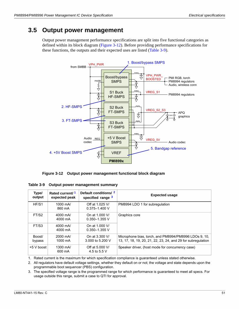
LM80-NT441-15 Rev. C 51
PMI8994/PMI8996 Power Management IC Device Specification Electrical specifications
3.5 Output power management
Output power management performance specifications are split into five functional categories as defined within its block diagram (Figure 3-12). Before providing performance specifications for these functions, the outputs and their expected uses are listed (Table 3-9).
Figure 3-12 Output power management functional block diagram
VPH_PWR
PMI899x
modeBoost/bypass
SMPS
+5 V Boost SMPS
VREF
S1 Buck HF-SMPS
S2 Buck FT-SMPS
S3 Buck FT-SMPS
Audio codecREQAudio
codec
APQgraphics
Audio, wireless conn
PMI RGB, torchVPH_PWR_BOOSTED
2. HF-SMPS
5. Bandgap reference
3. FT-SMPS
4. +5V Boost SMPS
from SMBB1. Boost/bypass SMPS
PM8994 regulators
PM8994 regulatorsVREG_S1
VREG_S2_S3
VREG_5V
Table 3-9 Output power management summary
Type/output
Rated current/ 11
expected peakDefault conditions/22
specified range33Expected usage
HF/S1 1000 mA/860 mA
Off at 1.025 V/0.375–1.400 V
PM8994 LDO 1 for subregulation
FT/S2 4000 mA/4000 mA
On at 1.000 V/0.350–1.355 V
Graphics core
FT/S3 4000 mA/4000 mA
On at 1.000 V/0.350–1.355 V
Boost/ bypass
2000 mA/1000 mA
On at 3.300 V/3.000 to 5.200 V
Microphone bias, torch, and PM8994/PM8996 LDOs 9, 10, 13, 17, 18, 19, 20, 21, 22, 23, 24, and 29 for subregulation
+5 V boost 1300 mA/600 mA
Off at 5.000 V/4.5 to 5.5 V
Speaker driver, (host mode for concurrency case)
1. Rated current is the maximum for which specification compliance is guaranteed unless stated otherwise.2. All regulators have default voltage settings, whether they default on or not; the voltage and state depends upon the
programmable boot sequencer (PBS) configuration.3. The specified voltage range is the programmed range for which performance is guaranteed to meet all specs. For
usage outside this range, submit a case to QTI for approval.
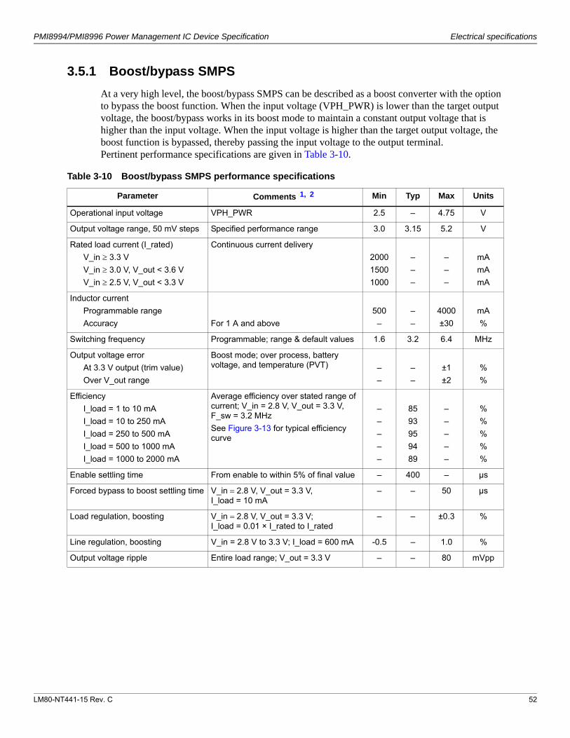
LM80-NT441-15 Rev. C 52
PMI8994/PMI8996 Power Management IC Device Specification Electrical specifications
3.5.1 Boost/bypass SMPS
At a very high level, the boost/bypass SMPS can be described as a boost converter with the option to bypass the boost function. When the input voltage (VPH_PWR) is lower than the target output voltage, the boost/bypass works in its boost mode to maintain a constant output voltage that is higher than the input voltage. When the input voltage is higher than the target output voltage, the boost function is bypassed, thereby passing the input voltage to the output terminal. Pertinent performance specifications are given in Table 3-10.
Table 3-10 Boost/bypass SMPS performance specifications
Parameter Comments11,22 Min Typ Max Units
Operational input voltage VPH_PWR 2.5 – 4.75 V
Output voltage range, 50 mV steps Specified performance range 3.0 3.15 5.2 V
Rated load current (I_rated)
V_in 3.3 V
V_in 3.0 V, V_out < 3.6 V
V_in 2.5 V, V_out < 3.3 V
Continuous current delivery
2000
1500
1000
–
–
–
–
–
–
mA
mA
mA
Inductor current
Programmable range
Accuracy For 1 A and above
500
–
–
–
4000
±30
mA
%
Switching frequency Programmable; range & default values 1.6 3.2 6.4 MHz
Output voltage error
At 3.3 V output (trim value)
Over V_out range
Boost mode; over process, battery voltage, and temperature (PVT) –
–
–
–
±1
±2
%
%
Efficiency
I_load = 1 to 10 mA
I_load = 10 to 250 mA
I_load = 250 to 500 mA
I_load = 500 to 1000 mA
I_load = 1000 to 2000 mA
Average efficiency over stated range of current; V_in = 2.8 V, V_out = 3.3 V, F_sw = 3.2 MHz
See Figure 3-13 for typical efficiency curve
–
–
–
–
–
85
93
95
94
89
–
–
–
–
–
%
%
%
%
%
Enable settling time From enable to within 5% of final value – 400 – µs
Forced bypass to boost settling time V_in 2.8 V, V_out = 3.3 V, I_load = 10 mA
– – 50 µs
Load regulation, boosting V_in 2.8 V, V_out = 3.3 V; I_load = 0.01 × I_rated to I_rated
– – ±0.3 %
Line regulation, boosting V_in = 2.8 V to 3.3 V; I_load = 600 mA -0.5 – 1.0 %
Output voltage ripple Entire load range; V_out = 3.3 V – – 80 mVpp
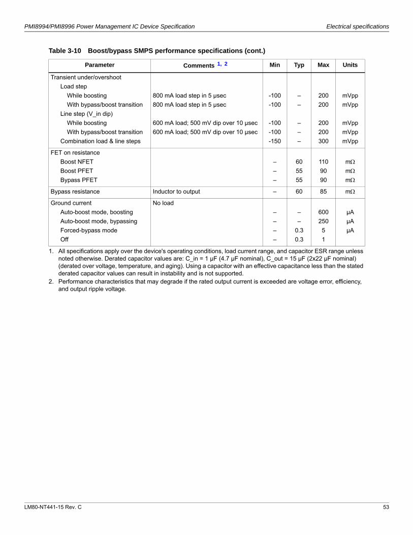
LM80-NT441-15 Rev. C 53
PMI8994/PMI8996 Power Management IC Device Specification Electrical specifications
Transient under/overshoot
Load step
While boosting
With bypass/boost transition
Line step (V_in dip)
While boosting
With bypass/boost transition
Combination load & line steps
800 mA load step in 5 µsec
800 mA load step in 5 µsec
600 mA load; 500 mV dip over 10 µsec
600 mA load; 500 mV dip over 10 µsec
-100
-100
-100
-100
-150
–
–
–
–
–
200
200
200
200
300
mVpp
mVpp
mVpp
mVpp
mVpp
FET on resistance
Boost NFET
Boost PFET
Bypass PFET
–
–
–
60
55
55
110
90
90
mmm
Bypass resistance Inductor to output – 60 85 m
Ground current
Auto-boost mode, boosting
Auto-boost mode, bypassing
Forced-bypass mode
Off
No load
–
–
–
–
–
–
0.3
0.3
600
250
5
1
µA
µA
µA
1. All specifications apply over the device's operating conditions, load current range, and capacitor ESR range unless noted otherwise. Derated capacitor values are: C_in = 1 µF (4.7 µF nominal), C_out = 15 µF (2x22 µF nominal) (derated over voltage, temperature, and aging). Using a capacitor with an effective capacitance less than the stated derated capacitor values can result in instability and is not supported.
2. Performance characteristics that may degrade if the rated output current is exceeded are voltage error, efficiency, and output ripple voltage.
Table 3-10 Boost/bypass SMPS performance specifications (cont.)
Parameter Comments11,22 Min Typ Max Units
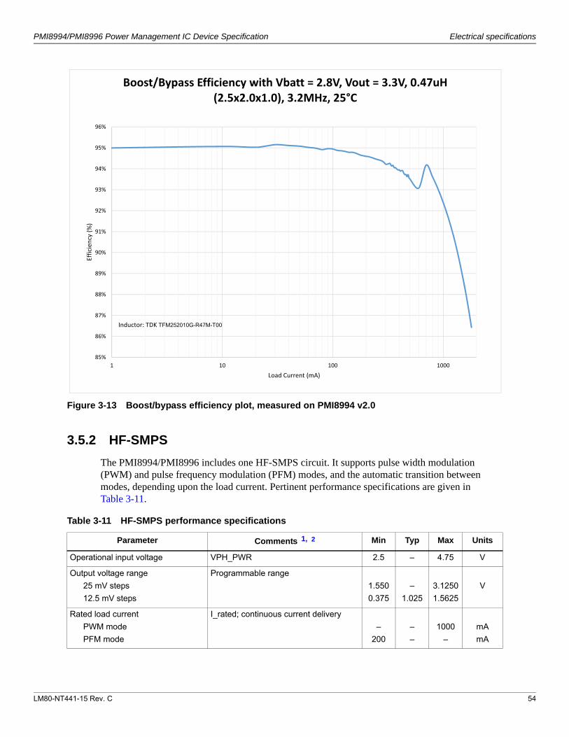
LM80-NT441-15 Rev. C 54
PMI8994/PMI8996 Power Management IC Device Specification Electrical specifications
Figure 3-13 Boost/bypass efficiency plot, measured on PMI8994 v2.0
3.5.2 HF-SMPS
The PMI8994/PMI8996 includes one HF-SMPS circuit. It supports pulse width modulation (PWM) and pulse frequency modulation (PFM) modes, and the automatic transition between modes, depending upon the load current. Pertinent performance specifications are given in Table 3-11.
85%
86%
87%
88%
89%
90%
91%
92%
93%
94%
95%
96%
1 10 100 1000
Efficiency(%
)
Load Current (mA)
Boost/Bypass Efficiency with Vbatt = 2.8V, Vout = 3.3V, 0.47uH(2.5x2.0x1.0), 3.2MHz, 25°C
Inductor: TDK TFM252010G-R47M-T00
Table 3-11 HF-SMPS performance specifications
Parameter Comments11, 2 Min Typ Max Units
Operational input voltage VPH_PWR 2.5 – 4.75 V
Output voltage range
25 mV steps
12.5 mV steps
Programmable range
1.550
0.375
–
1.025
3.1250
1.5625
V
Rated load current
PWM mode
PFM mode
I_rated; continuous current delivery
–
200
–
–
1000
–
mA
mA
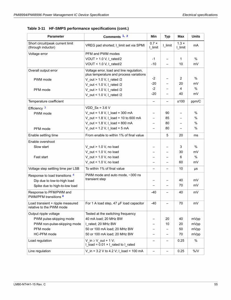
LM80-NT441-15 Rev. C 55
PMI8994/PMI8996 Power Management IC Device Specification Electrical specifications
Short circuit/peak current limit (through inductor)
VREG pad shorted; I_limit set via SPMI0.7 ×I_limit
I_limit1.3 ×I_limit
mA
Voltage error PFM and PWM modes
VOUT > 1.0 V, I_rated/2
VOUT < 1.0 V, I_rated/2
-1
-10
–
–
1
10
%
mV
Overall output error
PWM mode
PFM mode
Voltage error, load and line regulation, plus temperature and process variations
V_out > 1.0 V, I_rated /2
V_out < 1.0 V, I_rated /2
V_out > 1.0 V, I_rated /2
V_out < 1.0 V, I_rated /2
-2
-20
-2
-20
–
–
–
–
2
20
4
40
%
mV
%
mV
Temperature coefficient – – ±100 ppm/C
Efficiency33
PWM mode
PFM mode
VDD_Sx = 3.6 V
V_out = 1.8 V, I_load = 300 mA
V_out = 1.8 V, I_load = 10 to 600 mA
V_out = 1.8 V, I_load = 800 mA
V_out = 1.2 V, I_load = 5 mA
–
–
–
–
90
85
80
80
–
–
–
–
%
%
%
%
Enable settling time From enable to within 1% of final value 5 20 ms
Enable overshoot
Slow start
Fast start
V_out > 1.0 V, no load
V_out < 1.0 V, no load
V_out > 1.0 V, no load
V_out < 1.0 V, no load
–
–
–
–
–
–
–
–
3
30
6
60
%
mV
%
mV
Voltage step settling time per LSB To within 1% of final value – – 10 µs
Response to load transitions44
Dip due to low-to-high load
Spike due to high-to-low load
PWM mode and auto mode, ~300 ns transient step –
–
–
–
40
70
mV
mV
Response to PFM/PWM and PWM/PFM transitions 4
-40 – 40 mV
Load transient + ripple measured relative to the PWM mode
For 1 A load step, 47 µF load capacitor -40 – 70 mV
Output ripple voltage
PWM pulse-skipping mode
PWM non-pulse-skipping mode
PFM mode
HC-PFM mode
Tested at the switching frequency
40 mA load; 20 MHz BW
I_rated; 20 MHz BW
50 or 100 mA load; 20 MHz BW
50 or 100 mA load; 20 MHz BW
–
–
–
–
20
10
–
–
40
20
50
70
mVpp
mVpp
mVpp
mVpp
Load regulation V_in V_out + 1 V; I_load = 0.01 × I_rated to I_rated
– – 0.25 %
Line regulation V_in = 3.2 V to 4.2 V; I_load = 100 mA – – 0.25 %/V
Table 3-11 HF-SMPS performance specifications (cont.)
Parameter Comments11, 2 Min Typ Max Units

LM80-NT441-15 Rev. C 56
PMI8994/PMI8996 Power Management IC Device Specification Electrical specifications
Power-supply ripple rejection
50 Hz to 1 kHz
1 kHz to 100 kHz
100 kHz to 1 MHz
PSRR
40
20
30
–
–
–
–
–
–
dB
dB
dB
Output noise
F < 5 kHz
F = 5 kHz to 10 kHz
F = 10 kHz to 500 kHz
F = 500 kHz to 1 MHz
F > 2 MHz
–
–
–
–
–
-95
-100
-100
-110
-110
–
–
–
–
–
dBm/Hz
dBm/Hz
dBm/Hz
dBm/Hz
dBm/Hz
Ground current
PWM mode
PFM mode, auto
PFM mode, manual
No load
–
–
–
550
50
20
750
70
30
µA
µA
µA
1. All specifications apply over the device's operating conditions, load current range, and capacitor ESR range unless noted otherwise.
2. Performance characteristics that may degrade if the rated output current is exceeded are voltage error, efficiency, and output ripple voltage.
3. Figure 3-14 shows efficiency of S1 in auto mode.4. 400 mA load change within the range from I_rated/20 to I_rated. Note that larger load capacitors result in lower
voltage dips.
Table 3-11 HF-SMPS performance specifications (cont.)
Parameter Comments11, 2 Min Typ Max Units
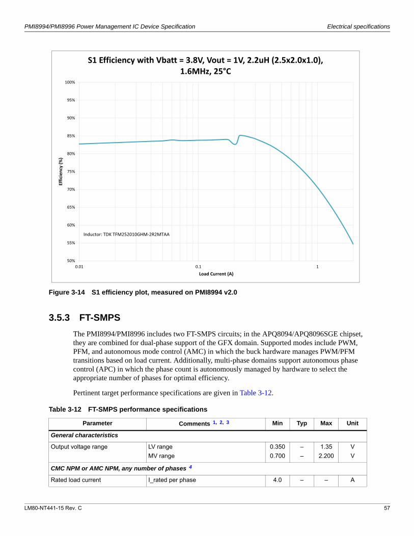
LM80-NT441-15 Rev. C 57
PMI8994/PMI8996 Power Management IC Device Specification Electrical specifications
Figure 3-14 S1 efficiency plot, measured on PMI8994 v2.0
3.5.3 FT-SMPS
The PMI8994/PMI8996 includes two FT-SMPS circuits; in the APQ8094/APQ8096SGE chipset, they are combined for dual-phase support of the GFX domain. Supported modes include PWM, PFM, and autonomous mode control (AMC) in which the buck hardware manages PWM/PFM transitions based on load current. Additionally, multi-phase domains support autonomous phase control (APC) in which the phase count is autonomously managed by hardware to select the appropriate number of phases for optimal efficiency.
Pertinent target performance specifications are given in Table 3-12.
50%
55%
60%
65%
70%
75%
80%
85%
90%
95%
100%
0.01 0.1 1
Efficiency(%
)
Load Current (A)
S1 Efficiency with Vbatt = 3.8V, Vout = 1V, 2.2uH (2.5x2.0x1.0),1.6MHz, 25°C
Inductor: TDK TFM252010GHM 2R2MTAA
Table 3-12 FT-SMPS performance specifications
Parameter Comments11,22,33 Min Typ Max Unit
General characteristics
Output voltage range LV range
MV range
0.350
0.700
–
–
1.35
2.200
V
V
CMC NPM or AMC NPM, any number of phases44
Rated load current I_rated per phase 4.0 – – A

LM80-NT441-15 Rev. C 58
PMI8994/PMI8996 Power Management IC Device Specification Electrical specifications
DC output voltage accuracy Including MBG, make tolerance, line and load regulation, and temperature (-30°C to 125°C)
VREG ≥ 0.8
VREG < 0.8
-2
-16
–
–
+2
+16
%
mV
Ripple voltage Measured across Cout where sense lines are tapped
Single-phase
Multi-phase
–
–
7
7
15
15
mVpp
mVpp
Line transient response GSM burst induced line transient represented by: Rbat = 350 mΩ; Istep = 2 A with 10 µs slew; VPH_PWR capacitance = 100 µF
– – 20 mVpp
CMC NPM or AMC NPM, multi-phase
Phase current mismatch Relative to ideal balanced current. -25 – +25 %
Ground current
Ground current (CMC NPM) No load, single-phase – 0.55 0.80 mA
Ground current per phase (CMC NPM or AMC NPM)
No load, multi-phase – 1.9 2.3 mA
Ground current (CMC LPM) No load, single- or multi-phase – 55 90 µA
Ground current per phase (AMC LPM)
No load, single- or multi-phase – 80 110 µA
CMC NPM or AMC load transient, any number of phases
Response to load transient (undershoot/overshoot)
1.5 A load step per phase for S2A/S12A, and 2 A load step per phase for all other domains; transient step ~100 ns, 1 V output
-50 – +80 mV
CMC LPM or AMC LPM, CPC or APC, any number of phases
DC output voltage accuracy Including MBG, make tolerance, line and load regulation, and temperature (-30°C to 125°C)
VSET ≥ 0.8V
VSET < 0.8V
-2
-16
–
–
+4
+32
%
mV
Ripple voltage Measured across Cout where sense lines are tapped
Single-phase
Multi-phase
–
–
25
20
40
35
mVpp
mVpp
CMC LPM, any number of phases
Rated load current CL_PFM = 1.404A – 0.8 – A
Transition specifications
Phase adding warm-up time NPM CPC change in phase count – 25 – µs
Table 3-12 FT-SMPS performance specifications (cont.)
Parameter Comments11,22,33 Min Typ Max Unit
LM80-NT441-15 Rev. C 59
PMI8994/PMI8996 Power Management IC Device Specification Electrical specifications
Phase current settling time Time to achieve phase current match
Steady state loading; all active phases in CCM; change in phase count
– – 200 µs
Other general characteristics
Efficiency See Figure 3-15 for typical efficiency plot – – – %
Enable settling time Vout slewing to within 1% of final value – 100 µs
Voltage stepper undershoot/overshoot
1 LSB step slewing -5 – +5 mV
Peak output impedance 1 kHz to 1 MHz – – 40 mΩ
Discharge impedance – 32 – Ω
1. General specifications for the FTS 2.5 apply overall operating conditions of supply, temperature, process, and component variances except where noted.
2. Default components are assumed (470 nH, 2x 22 µF per phase) along with deployed configurations for the APQ8094/APQ8096SGE lineup.
3. Where parametric performance is influenced by external components, baseline components are assumed. Values listed are the component specified values, not the derated values. Derating must be taken into account to ensure robustness. Initial assumption is 50% derating on capacitors pending further assessment of specific component selections (rough allowance for temperature, tolerance, and voltage derating).
4. Acronyms are: low-power mode (LPM), normal power mode (NPM), autonomous mode control (AMC), commended (forced) mode control (CMC), autonomous phase control (APC), and commended (forced) phase control (CPC).
Table 3-12 FT-SMPS performance specifications (cont.)
Parameter Comments11,22,33 Min Typ Max Unit
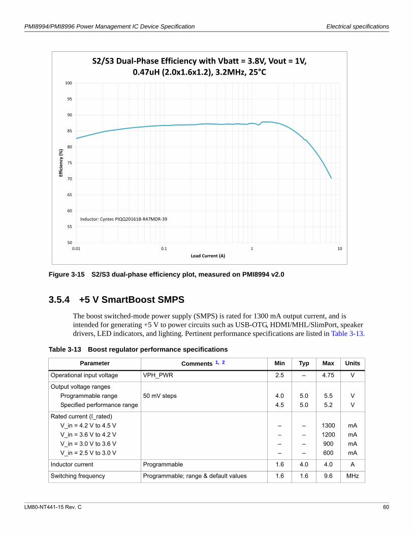
LM80-NT441-15 Rev. C 60
PMI8994/PMI8996 Power Management IC Device Specification Electrical specifications
Figure 3-15 S2/S3 dual-phase efficiency plot, measured on PMI8994 v2.0
3.5.4 +5 V SmartBoost SMPS
The boost switched-mode power supply (SMPS) is rated for 1300 mA output current, and is intended for generating +5 V to power circuits such as USB-OTG, HDMI/MHL/SlimPort, speaker drivers, LED indicators, and lighting. Pertinent performance specifications are listed in Table 3-13.
50
55
60
65
70
75
80
85
90
95
100
0.01 0.1 1 10
Efficiency(%
)
Load Current (A)
S2/S3 Dual Phase Efficiency with Vbatt = 3.8V, Vout = 1V,0.47uH (2.0x1.6x1.2), 3.2MHz, 25°C
Inductor: Cyntec PIQQ20161B R47MDR 39
Table 3-13 Boost regulator performance specifications
Parameter Comments11,22 Min Typ Max Units
Operational input voltage VPH_PWR 2.5 – 4.75 V
Output voltage ranges
Programmable range
Specified performance range
50 mV steps 4.0
4.5
5.0
5.0
5.5
5.2
V
V
Rated current (I_rated)
V_in = 4.2 V to 4.5 V
V_in = 3.6 V to 4.2 V
V_in = 3.0 V to 3.6 V
V_in = 2.5 V to 3.0 V
–
–
–
–
–
–
–
–
1300
1200
900
600
mA
mA
mA
mA
Inductor current Programmable 1.6 4.0 4.0 A
Switching frequency Programmable; range & default values 1.6 1.6 9.6 MHz
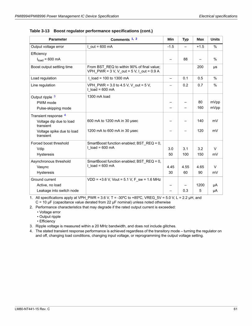
LM80-NT441-15 Rev. C 61
PMI8994/PMI8996 Power Management IC Device Specification Electrical specifications
Output voltage error I_out = 600 mA -1.5 – +1.5 %
Efficiency
Iload = 600 mA – 88 – %
Boost output settling time From BST_REQ to within 90% of final value; VPH_PWR = 3 V, V_out = 5 V, I_out = 0.9 A
200 µs
Load regulation I_load = 100 to 1300 mA – 0.1 0.5 %
Line regulation VPH_PWR = 3.0 to 4.5 V, V_out = 5 V, I_load = 600 mA
– 0.2 0.7 %
Output ripple33
PWM mode
Pulse-skipping mode
1300 mA load
–
–
–
–
80
160
mVpp
mVpp
Transient response44
Voltage dip due to load transient
Voltage spike due to load transient
600 mA to 1200 mA in 30 µsec
1200 mA to 600 mA in 30 µsec
–
–
–
–
140
120
mV
mV
Forced boost threshold
Vdip
Hysteresis
SmartBoost function enabled; BST_REQ = 0, I_load = 600 mA 3.0
50
3.1
100
3.2
150
V
mV
Asynchronous threshold
Vasync
Hysteresis
SmartBoost function enabled; BST_REQ = 0, I_load = 600 mA 4.45
30
4.55
60
4.65
90
V
mV
Ground current
Active, no load
Leakage into switch node
VDD = +3.6 V, Vout = 5.1 V, F_sw = 1.6 MHz
–
–
–
0.3
1200
5
µA
µA
1. All specifications apply at VPH_PWR = 3.6 V, T = -30ºC to +85ºC, VREG_5V = 5.0 V, L = 2.2 µH, and C = 10 µF (capacitance value derated from 22 µF nominal) unless noted otherwise
2. Performance characteristics that may degrade if the rated output current is exceeded:• Voltage error• Output ripple• Efficiency
3. Ripple voltage is measured within a 20 MHz bandwidth, and does not include glitches.4. The stated transient response performance is achieved regardless of the transitory mode – turning the regulator on
and off, changing load conditions, changing input voltage, or reprogramming the output voltage setting.
Table 3-13 Boost regulator performance specifications (cont.)
Parameter Comments11,22 Min Typ Max Units
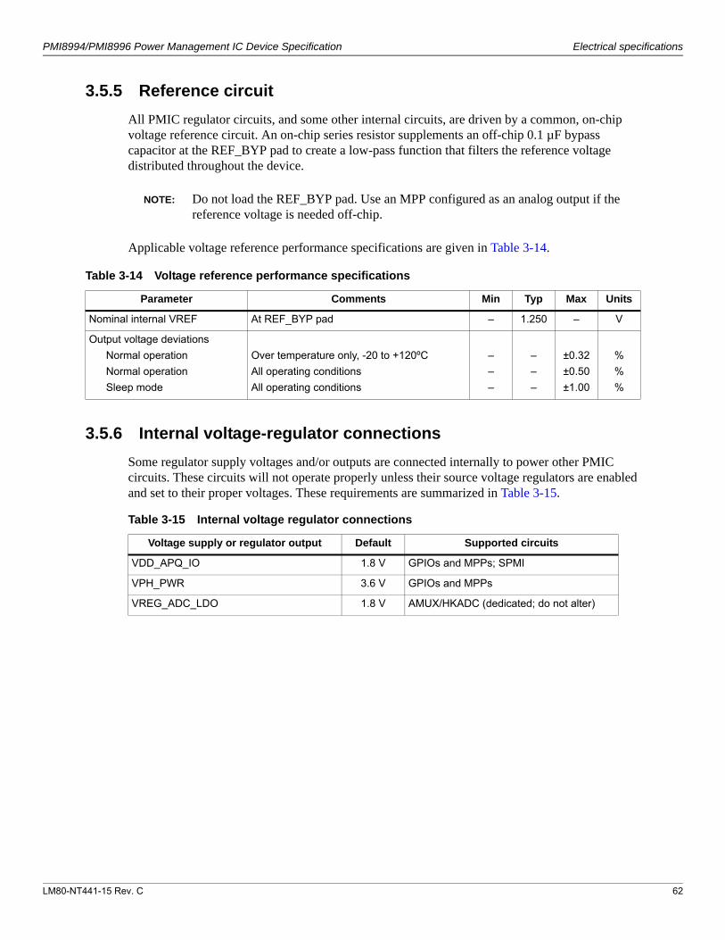
LM80-NT441-15 Rev. C 62
PMI8994/PMI8996 Power Management IC Device Specification Electrical specifications
3.5.5 Reference circuit
All PMIC regulator circuits, and some other internal circuits, are driven by a common, on-chip voltage reference circuit. An on-chip series resistor supplements an off-chip 0.1 µF bypass capacitor at the REF_BYP pad to create a low-pass function that filters the reference voltage distributed throughout the device.
NOTE: Do not load the REF_BYP pad. Use an MPP configured as an analog output if the reference voltage is needed off-chip.
Applicable voltage reference performance specifications are given in Table 3-14.
3.5.6 Internal voltage-regulator connections
Some regulator supply voltages and/or outputs are connected internally to power other PMIC circuits. These circuits will not operate properly unless their source voltage regulators are enabled and set to their proper voltages. These requirements are summarized in Table 3-15.
Table 3-14 Voltage reference performance specifications
Parameter Comments Min Typ Max Units
Nominal internal VREF At REF_BYP pad – 1.250 – V
Output voltage deviations
Normal operation
Normal operation
Sleep mode
Over temperature only, -20 to +120ºC
All operating conditions
All operating conditions
–
–
–
–
–
–
±0.32
±0.50
±1.00
%
%
%
Table 3-15 Internal voltage regulator connections
Voltage supply or regulator output Default Supported circuits
VDD_APQ_IO 1.8 V GPIOs and MPPs; SPMI
VPH_PWR 3.6 V GPIOs and MPPs
VREG_ADC_LDO 1.8 V AMUX/HKADC (dedicated; do not alter)
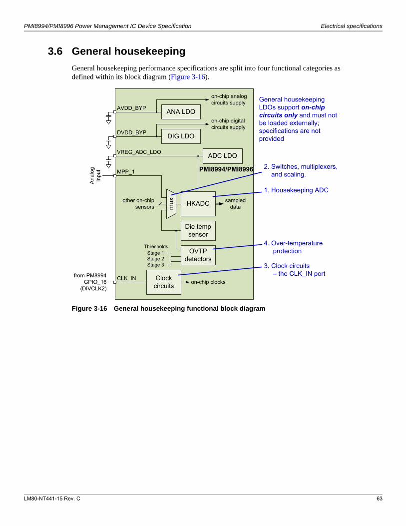
LM80-NT441-15 Rev. C 63
PMI8994/PMI8996 Power Management IC Device Specification Electrical specifications
3.6 General housekeeping
General housekeeping performance specifications are split into four functional categories as defined within its block diagram (Figure 3-16).
Figure 3-16 General housekeeping functional block diagram
HKADC
Anal
og
inpu
t
CLK_IN
sampled data
PMI8994/PMI8996
ADC LDO
on-chip analog circuits supply
AVDD_BYP
DVDD_BYP
ANA LDO
DIG LDO
MPP_1
from PM8994GPIO_16
(DIVCLK2)
VREG_ADC_LDO
on-chip digital circuits supply
1. Housekeeping ADC
3. Clock circuits – the CLK_IN port
General housekeeping LDOs support on-chipcircuits only and must not be loaded externally; specifications are not provided
Die temp sensor
Stage 1 OVTPdetectorsStage 2
Stage 3
mux
Thresholds
other on-chip sensors
on-chip clocksClockcircuits
4. Over-temperature protection
2. Switches, multiplexers, and scaling.

LM80-NT441-15 Rev. C 64
PMI8994/PMI8996 Power Management IC Device Specification Electrical specifications
3.6.1 Analog multiplexer and scaling circuits
Analog switches, multiplexers, and voltage-scaling circuits select and condition a single analog signal for routing to the on-chip HKADC. Available multiplexer and scaling functions are summarized in Table 3-16.
NOTE: Gain and offset errors are different through each analog multiplexer channel. Each path should be calibrated individually over its valid gain and offset settings for best accuracy.
Performance specifications pertaining to the analog multiplexer and its associated circuits are listed in Table 3-17.
Table 3-16 Analog multiplexer and scaling functions
Ch # Description Typical input range (V)11 Scaling Typical output range (V)
0 USB_IN 3 to 10 1/20 0.15 to 0.50
1 DC_IN 3 to 10 1/20 0.15 to 0.50
9 0.625 V reference voltage 0.625 1 0.625
10 1.25 V reference voltage 1.25 1 1.25
12 0.625 V reference voltage buffer 0.625 1 0.625
13 Die-temperature monitor 0.4 to 0.9 1 0.4 to 0.9
14 GND_REF Direct connection to ADC for calibration
15 VDD_ADC Direct connection to ADC for calibration
16 MPP_1 0.05 to 1.5 1 0.05 to 1.5
32 MPP_1 0.3 to VPH_PWR 1/3 0.1 to 1.70
63 Module power off22 – – –
67 USB_DP 0.3 to VPH_PWR 1/3 0.1 to 1.70
68 USB_DM 0.3 to VPH_PWR 1/3 0.1 to 1.70
1. Input voltage must not exceed the ADC reference voltage generated by VREG_ADC_LDO (1.8 V).2. Channel 32 should be selected when the analog multiplexer is not being used; this prevents the scalers from
loading the inputs.
Table 3-17 Analog multiplexer performance specifications
Parameter Comments11 Min Typ Max Units
Operational input voltage (Vadc) Connected internally to VREG_ADC – 1.8 – V
Output voltage range
Full specification compliance
Degraded accuracy at edges
0.10
0.05
–
–
Vadc – 0.10
Vadc – 0.05
V
V
Input referred offset errors
Channels with x1 scaling
Channels with 1/3 scaling
Channels with 1/20 scaling
–
–
–
–
–
–
±2.0
±1.5
±2.0
mV
mV
mV
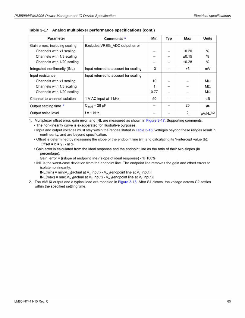
LM80-NT441-15 Rev. C 65
PMI8994/PMI8996 Power Management IC Device Specification Electrical specifications
Gain errors, including scaling
Channels with x1 scaling
Channels with 1/3 scaling
Channels with 1/20 scaling
Excludes VREG_ADC output error
–
–
–
–
–
–
±0.20
±0.15
±0.28
%
%
%
Integrated nonlinearity (INL) Input referred to account for scaling -3 – +3 mV
Input resistance
Channels with x1 scaling
Channels with 1/3 scaling
Channels with 1/20 scaling
Input referred to account for scaling
10
1
0.77
–
–
–
–
–
–
MMM
Channel-to-channel isolation 1 V AC input at 1 kHz 50 – – dB
Output settling time22 Cload = 28 pF – – 25 µs
Output noise level f = 1 kHz – – 2 µV/Hz1/2
1. Multiplexer offset error, gain error, and INL are measured as shown in Figure 3-17. Supporting comments:• The non-linearity curve is exaggerated for illustrative purposes.• Input and output voltages must stay within the ranges stated in Table 3-16; voltages beyond these ranges result in
nonlinearity, and are beyond specification.• Offset is determined by measuring the slope of the endpoint line (m) and calculating its Y-intercept value (b):
Offset = b = y1 - m·x1• Gain error is calculated from the ideal response and the endpoint line as the ratio of their two slopes (in
percentage):Gain_error = [(slope of endpoint line)/(slope of ideal response) - 1]·100%
• INL is the worst-case deviation from the endpoint line. The endpoint line removes the gain and offset errors to isolate nonlinearity:INL(min) = min[Vout(actual at Vx input) - Vout(endpoint line at Vx input)]INL(max) = max[Vout(actual at Vx input) - Vout(endpoint line at Vx input)]
2. The AMUX output and a typical load are modeled in Figure 3-18. After S1 closes, the voltage across C2 settles within the specified settling time.
Table 3-17 Analog multiplexer performance specifications (cont.)
Parameter Comments11 Min Typ Max Units

LM80-NT441-15 Rev. C 66
PMI8994/PMI8996 Power Management IC Device Specification Electrical specifications
Figure 3-17 Multiplexer offset and gain errors
Figure 3-18 Analog multiplexer load condition for settling time specification
outputvoltagerange
Y-intercept of endpoint line= offset voltage
endpoint line
actual cu
rve
INL(min)
INL(max)
ideal curve
V(in)
V(ou
t)
S1AMUX_OUT
C2C1 V(out)
sampling switch (1 k maximum)
parasitic capacitance (0 to 20 pF)
sampling capacitor (63 pF)
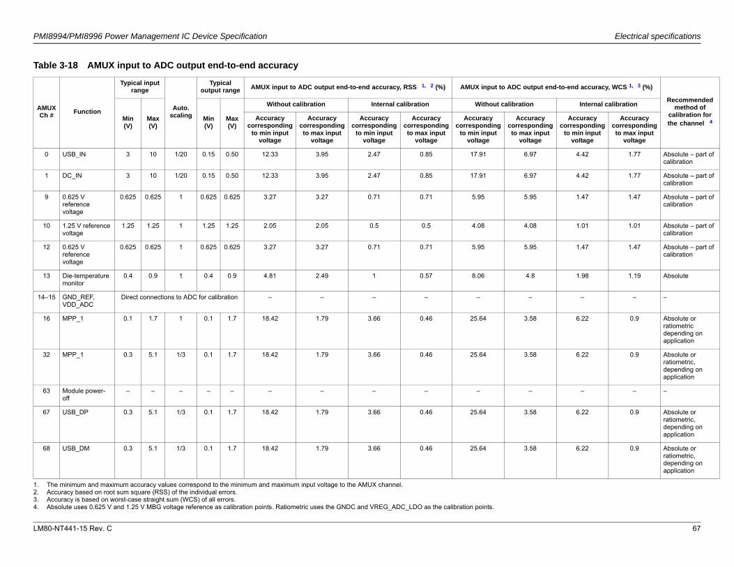
PMI8994/PMI8996 Power Management IC Device Specification Electrical specifications
LM80-NT441-15 Rev. C 67
Table 3-18 AMUX input to ADC output end-to-end accuracy
AMUX Ch #
Function
Typical input range
Auto. scaling
Typical output range AMUX input to ADC output end-to-end accuracy, RSS 11, 22 (%)
1. The minimum and maximum accuracy values correspond to the minimum and maximum input voltage to the AMUX channel.2. Accuracy based on root sum square (RSS) of the individual errors.
AMUX input to ADC output end-to-end accuracy, WCS 1, 33 (%)
3. Accuracy is based on worst-case straight sum (WCS) of all errors.
Recommended method of
calibration for the channel 44
4. Absolute uses 0.625 V and 1.25 V MBG voltage reference as calibration points. Ratiometric uses the GNDC and VREG_ADC_LDO as the calibration points.
Min (V)
Max (V)
Min (V)
Max (V)
Without calibration Internal calibration Without calibration Internal calibration
Accuracy corresponding
to min input voltage
Accuracy corresponding to max input
voltage
Accuracy corresponding
to min input voltage
Accuracy corresponding to max input
voltage
Accuracy corresponding
to min input voltage
Accuracy corresponding to max input
voltage
Accuracy corresponding
to min input voltage
Accuracy corresponding to max input
voltage
0 USB_IN 3 10 1/20 0.15 0.50 12.33 3.95 2.47 0.85 17.91 6.97 4.42 1.77 Absolute – part of calibration
1 DC_IN 3 10 1/20 0.15 0.50 12.33 3.95 2.47 0.85 17.91 6.97 4.42 1.77 Absolute – part of calibration
9 0.625 V reference voltage
0.625 0.625 1 0.625 0.625 3.27 3.27 0.71 0.71 5.95 5.95 1.47 1.47 Absolute – part of calibration
10 1.25 V reference voltage
1.25 1.25 1 1.25 1.25 2.05 2.05 0.5 0.5 4.08 4.08 1.01 1.01 Absolute – part of calibration
12 0.625 V reference voltage
0.625 0.625 1 0.625 0.625 3.27 3.27 0.71 0.71 5.95 5.95 1.47 1.47 Absolute – part of calibration
13 Die-temperature monitor
0.4 0.9 1 0.4 0.9 4.81 2.49 1 0.57 8.06 4.8 1.98 1.19 Absolute
14–15 GND_REF, VDD_ADC
Direct connections to ADC for calibration – – – – – – – – –
16 MPP_1 0.1 1.7 1 0.1 1.7 18.42 1.79 3.66 0.46 25.64 3.58 6.22 0.9 Absolute or ratiometric depending on application
32 MPP_1 0.3 5.1 1/3 0.1 1.7 18.42 1.79 3.66 0.46 25.64 3.58 6.22 0.9 Absolute or ratiometric, depending on application
63 Module power-off
– – – – – – – – – – – – – –
67 USB_DP 0.3 5.1 1/3 0.1 1.7 18.42 1.79 3.66 0.46 25.64 3.58 6.22 0.9 Absolute or ratiometric, depending on application
68 USB_DM 0.3 5.1 1/3 0.1 1.7 18.42 1.79 3.66 0.46 25.64 3.58 6.22 0.9 Absolute or ratiometric, depending on application
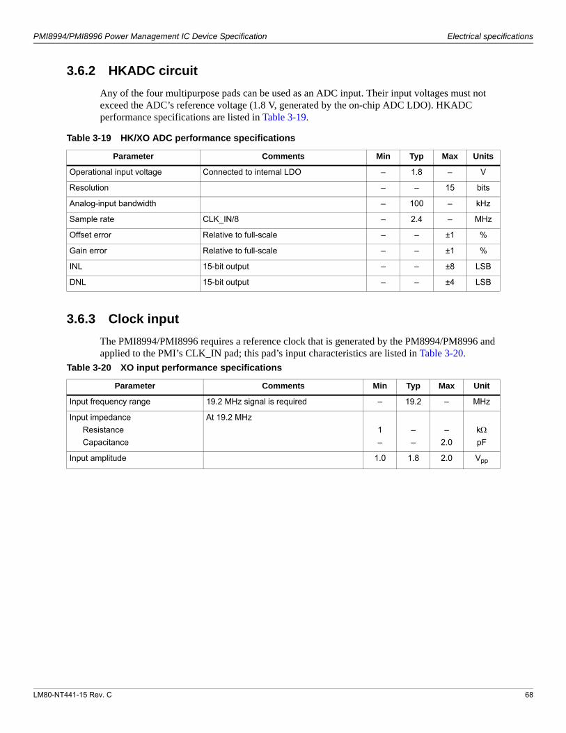
LM80-NT441-15 Rev. C 68
PMI8994/PMI8996 Power Management IC Device Specification Electrical specifications
3.6.2 HKADC circuit
Any of the four multipurpose pads can be used as an ADC input. Their input voltages must not exceed the ADC’s reference voltage (1.8 V, generated by the on-chip ADC LDO). HKADC performance specifications are listed in Table 3-19.
3.6.3 Clock input
The PMI8994/PMI8996 requires a reference clock that is generated by the PM8994/PM8996 and applied to the PMI’s CLK_IN pad; this pad’s input characteristics are listed in Table 3-20.
Table 3-19 HK/XO ADC performance specifications
Parameter Comments Min Typ Max Units
Operational input voltage Connected to internal LDO – 1.8 – V
Resolution – – 15 bits
Analog-input bandwidth – 100 – kHz
Sample rate CLK_IN/8 – 2.4 – MHz
Offset error Relative to full-scale – – ±1 %
Gain error Relative to full-scale – – ±1 %
INL 15-bit output – – ±8 LSB
DNL 15-bit output – – ±4 LSB
Table 3-20 XO input performance specifications
Parameter Comments Min Typ Max Unit
Input frequency range 19.2 MHz signal is required – 19.2 – MHz
Input impedance
Resistance
Capacitance
At 19.2 MHz
1
–
–
–
–
2.0
kpF
Input amplitude 1.0 1.8 2.0 Vpp

LM80-NT441-15 Rev. C 69
PMI8994/PMI8996 Power Management IC Device Specification Electrical specifications
3.6.4 Over-temperature protection (smart thermal control)
The PMIC includes over-temperature protection in stages, depending on the level of urgency as the die temperature rises:
Stage 0 – normal operating conditions.
Stage 1 – 90°C to 100°C (configurable threshold); an interrupt is sent to the MDM without shutting down any PMIC circuits.
Temperature hysteresis is incorporated, such that the die temperature must cool significantly before the device can be powered on again. If any start signals are present while at Stage 3, they are ignored until Stage 0 is reached. When the device cools enough to reach Stage 0 and a start signal is present, the PMIC will power up immediately.
3.7 User interfaces
User interfaces performance specifications are split into six functional categories as defined within its block diagram (Figure 3-19).

PMI8994/PMI8996 Power Management IC Device Specification Electrical specifications
LM80-NT441-15 Rev. C 70
Figure 3-19 User interface functional block diagram
internalinterface
HapticsLRA/ERM
RGB_RED
RGB_GRN
MPP_xx
MPP_yy
HAP_OUT_P
MPP
co
nfig
RGB_BLU
VDD_FLASH
VDD_RGB
VDD_TORCH
FLSH_LED1 (2)
VSNS_FLSH
Cur
rent
cont
rols
FLSH_LED2 (2)
HAP_OUT_N
PMI8994/PMI8996
HAP_PWM_IN
VDD_FLASH_C
Flash support
GND_HAP
VDD_HAP
Cur
rent
cont
rols
3-ch
ligh
t pu
lse
gen
Cur
rent
co
ntro
ls
3. Flash drivers(including torch mode)
1. Haptics
2. Display ± bias
4. White LEDs
5. Other current drivers and current sinks
6. LPG
VSW_WLED
VREG_WLED
WLED_SINK2
WLED_SINK3
WLED_CABC
VDD_WLED
GND_WLED
WLED28.5 VSMPS
Cur
rent
cont
rols
WLED_SINK1
WLED_SINK4
GND_WLED_I
from
di
spla
y
WLED strings
VPH_PWR
VSW_DIS_P
DIS_P_FB
VDD_DIS_P
GND_DIS_P
DisplaypositiveSMPS
DIS_SCTRL
Displaynegative SMPS
DIS_P_OUT
VSW_DIS_N
DIS_N_FB
VDD_DIS_N
DIS_N_OUT
VDD_1P8_DIS_N
DIS_N_CAP_REF
VPH_PWR
VPH_PWR
+5.5 V
from display
1.8 V
GND_DIS_N_REF
-5.5 V
VPH_PWR_BOOSTED
VPH_PWR
VPH_PWR_BOOSTED
DC_IN_OUT
VPH_PWR
LRA or ERM
digital PWM or audio
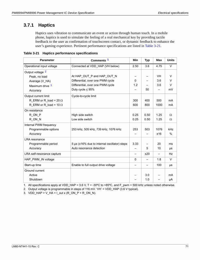
LM80-NT441-15 Rev. C 71
PMI8994/PMI8996 Power Management IC Device Specification Electrical specifications
3.7.1 Haptics
Haptics uses vibration to communicate an event or action through human touch. In a mobile phone, haptics is used to simulate the feeling of a real mechanical key by providing tactile feedback to the user as confirmation of touchscreen contact, or dynamic feedback to enhance the user’s gaming experience. Pertinent performance specifications are listed in Table 3-21.
Table 3-21 Haptics performance specifications
Parameter Comments11
1. All specifications apply at VDD_HAP = 3.6 V, T = -30ºC to +85ºC, and F_pwm = 500 kHz unless noted otherwise.
Min Typ Max Units
Operational input voltage Connected at VDD_HAP (VH below) 2.50 3.6 4.75 V
Output voltage22
Peak, no load
Average (V_HA)
Maximum drive33
Accuracy
2. Output voltage is programmable in steps of 116 mV. ‘VH’ = VDD_HAP (3.6 V typical).3. VDD_HAP > V_HA + I_out x (R_ON_P + R_ON_N).
At HAP_OUT_P and HAP_OUT_N
Differential, over one PWM cycle
Differential, over one PWM cycle
Duty cycle < 95%
–
0
1.2
–
–
–
–
50
VH
3.6
3.6
–
V
V
V
mV
Output current limit
R_ERM or R_load = 20 R_ERM or R_load = 10
Cycle-to-cycle limit
300
600
400
800
500
1000
mA
mA
On resistance
R_ON_P
R_ON_N
High side switch
Low side switch
0.25
0.25
0.50
0.50
1.25
1.25
Internal PWM frequency
Programmable options
Accuracy
253 kHz, 505 kHz, 739 kHz, 1076 kHz 253
–
503
–
1076
±16
kHz
%
LRA resonance
Programmable period
Accuracy
5 µs (±16% due to internal oscillator) steps
Auto resonance detection
3.33
–
–
5
20
10
ms
µs
LRA self-resonance capture – ±20 – Hz
HAP_PWM_IN voltage 0 – 1.8 V
Start-up time Enable to full output drive voltage – – 100 µs
Ground current
Active
Shutdown
–
–
3.0
1.0
–
–
mA
µA
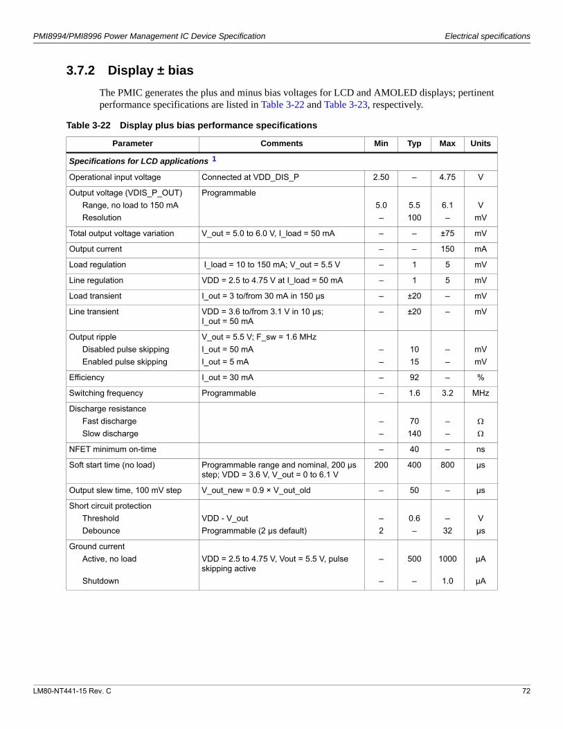
LM80-NT441-15 Rev. C 72
PMI8994/PMI8996 Power Management IC Device Specification Electrical specifications
3.7.2 Display ± bias
The PMIC generates the plus and minus bias voltages for LCD and AMOLED displays; pertinent performance specifications are listed in Table 3-22 and Table 3-23, respectively.
Table 3-22 Display plus bias performance specifications
Parameter Comments Min Typ Max Units
Specifications for LCD applications11
Operational input voltage Connected at VDD_DIS_P 2.50 – 4.75 V
Output voltage (VDIS_P_OUT)
Range, no load to 150 mA
Resolution
Programmable
5.0
–
5.5
100
6.1
–
V
mV
Total output voltage variation V_out = 5.0 to 6.0 V, I_load = 50 mA – – ±75 mV
Output current – – 150 mA
Load regulation I_load = 10 to 150 mA; V_out = 5.5 V – 1 5 mV
Line regulation VDD = 2.5 to 4.75 V at I_load = 50 mA – 1 5 mV
Load transient I_out = 3 to/from 30 mA in 150 µs – ±20 – mV
Line transient VDD = 3.6 to/from 3.1 V in 10 µs; I_out = 50 mA
– ±20 – mV
Output ripple
Disabled pulse skipping
Enabled pulse skipping
V_out = 5.5 V; F_sw = 1.6 MHz
I_out = 50 mA
I_out = 5 mA
–
–
10
15
–
–
mV
mV
Efficiency I_out = 30 mA – 92 – %
Switching frequency Programmable – 1.6 3.2 MHz
Discharge resistance
Fast discharge
Slow discharge
–
–
70
140
–
–
NFET minimum on-time – 40 – ns
Soft start time (no load) Programmable range and nominal, 200 µs step; VDD = 3.6 V, V_out = 0 to 6.1 V
200 400 800 µs
Output slew time, 100 mV step V_out_new = 0.9 × V_out_old – 50 – µs
Short circuit protection
Threshold
Debounce
VDD - V_out
Programmable (2 µs default)
–
2
0.6
–
–
32
V
µs
Ground current
Active, no load
Shutdown
VDD = 2.5 to 4.75 V, Vout = 5.5 V, pulse skipping active
–
–
500
–
1000
1.0
µA
µA
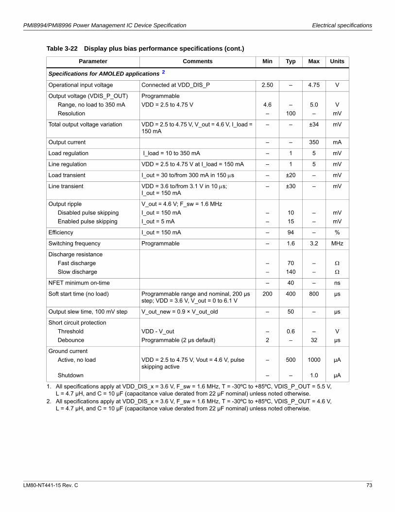
LM80-NT441-15 Rev. C 73
PMI8994/PMI8996 Power Management IC Device Specification Electrical specifications
Specifications for AMOLED applications22
Operational input voltage Connected at VDD_DIS_P 2.50 – 4.75 V
Output voltage (VDIS_P_OUT)
Range, no load to 350 mA
Resolution
Programmable
VDD = 2.5 to 4.75 V 4.6
–
–
100
5.0
–
V
mV
Total output voltage variation VDD = 2.5 to 4.75 V, V_out = 4.6 V, I_load = 150 mA
– – ±34 mV
Output current – – 350 mA
Load regulation I_load = 10 to 350 mA – 1 5 mV
Line regulation VDD = 2.5 to 4.75 V at I_load = 150 mA – 1 5 mV
Load transient I_out = 30 to/from 300 mA in 150 s – ±20 – mV
Line transient VDD = 3.6 to/from 3.1 V in 10 s; I_out = 150 mA
– ±30 – mV
Output ripple
Disabled pulse skipping
Enabled pulse skipping
V_out = 4.6 V; F_sw = 1.6 MHz
I_out = 150 mA
I_out = 5 mA
–
–
10
15
–
–
mV
mV
Efficiency I_out = 150 mA – 94 – %
Switching frequency Programmable – 1.6 3.2 MHz
Discharge resistance
Fast discharge
Slow discharge
–
–
70
140
–
–
NFET minimum on-time – 40 – ns
Soft start time (no load) Programmable range and nominal, 200 µs step; VDD = 3.6 V, V_out = 0 to 6.1 V
200 400 800 µs
Output slew time, 100 mV step V_out_new = 0.9 × V_out_old – 50 – µs
Short circuit protection
Threshold
Debounce
VDD - V_out
Programmable (2 µs default)
–
2
0.6
–
–
32
V
µs
Ground current
Active, no load
Shutdown
VDD = 2.5 to 4.75 V, Vout = 4.6 V, pulse skipping active
–
–
500
–
1000
1.0
µA
µA
1. All specifications apply at VDD_DIS_x = 3.6 V, F_sw = 1.6 MHz, T = -30ºC to +85ºC, VDIS_P_OUT = 5.5 V, L = 4.7 µH, and C = 10 µF (capacitance value derated from 22 µF nominal) unless noted otherwise.
2. All specifications apply at VDD_DIS_x = 3.6 V, F_sw = 1.6 MHz, T = -30ºC to +85ºC, VDIS_P_OUT = 4.6 V, L = 4.7 µH, and C = 10 µF (capacitance value derated from 22 µF nominal) unless noted otherwise.
Table 3-22 Display plus bias performance specifications (cont.)
Parameter Comments Min Typ Max Units
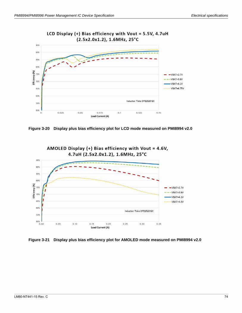
LM80-NT441-15 Rev. C 74
PMI8994/PMI8996 Power Management IC Device Specification Electrical specifications
Figure 3-20 Display plus bias efficiency plot for LCD mode measured on PMI8994 v2.0
Figure 3-21 Display plus bias efficiency plot for AMOLED mode measured on PMI8994 v2.0
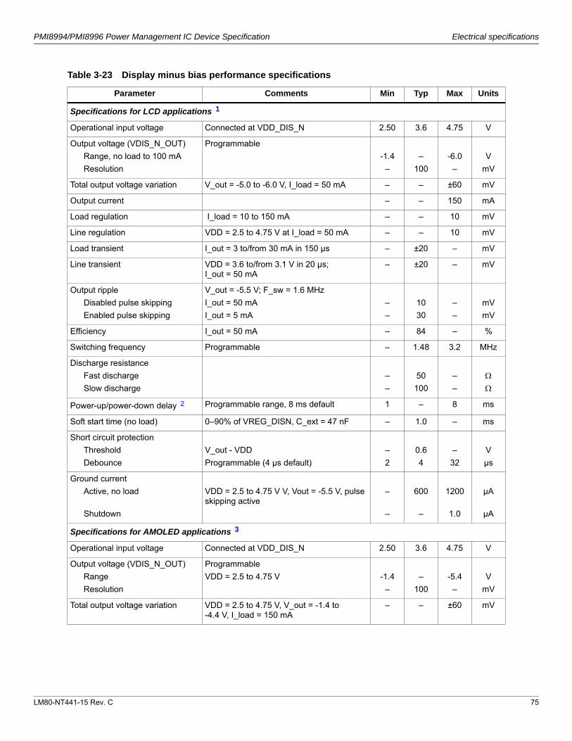
LM80-NT441-15 Rev. C 75
PMI8994/PMI8996 Power Management IC Device Specification Electrical specifications
Table 3-23 Display minus bias performance specifications
Parameter Comments Min Typ Max Units
Specifications for LCD applications11
Operational input voltage Connected at VDD_DIS_N 2.50 3.6 4.75 V
Output voltage (VDIS_N_OUT)
Range, no load to 100 mA
Resolution
Programmable
-1.4
–
–
100
-6.0
–
V
mV
Total output voltage variation V_out = -5.0 to -6.0 V, I_load = 50 mA – – ±60 mV
Output current – – 150 mA
Load regulation I_load = 10 to 150 mA – – 10 mV
Line regulation VDD = 2.5 to 4.75 V at I_load = 50 mA – – 10 mV
Load transient I_out = 3 to/from 30 mA in 150 µs – ±20 – mV
Line transient VDD = 3.6 to/from 3.1 V in 20 µs; I_out = 50 mA
– ±20 – mV
Output ripple
Disabled pulse skipping
Enabled pulse skipping
V_out = -5.5 V; F_sw = 1.6 MHz
I_out = 50 mA
I_out = 5 mA
–
–
10
30
–
–
mV
mV
Efficiency I_out = 50 mA – 84 – %
Switching frequency Programmable – 1.48 3.2 MHz
Discharge resistance
Fast discharge
Slow discharge
–
–
50
100
–
–
Power-up/power-down delay22 Programmable range, 8 ms default 1 – 8 ms
Soft start time (no load) 0–90% of VREG_DISN, C_ext = 47 nF – 1.0 – ms
Short circuit protection
Threshold
Debounce
V_out - VDD
Programmable (4 µs default)
–
2
0.6
4
–
32
V
µs
Ground current
Active, no load
Shutdown
VDD = 2.5 to 4.75 V V, Vout = -5.5 V, pulse skipping active
–
–
600
–
1200
1.0
µA
µA
Specifications for AMOLED applications33
Operational input voltage Connected at VDD_DIS_N 2.50 3.6 4.75 V
Output voltage (VDIS_N_OUT)
Range
Resolution
Programmable
VDD = 2.5 to 4.75 V -1.4
–
–
100
-5.4
–
V
mV
Total output voltage variation VDD = 2.5 to 4.75 V, V_out = -1.4 to -4.4 V, I_load = 150 mA
– – ±60 mV

LM80-NT441-15 Rev. C 76
PMI8994/PMI8996 Power Management IC Device Specification Electrical specifications
Output current
VPH_PWR = 2.85 to 4.75 V
VPH_PWR = 2.65 to 4.75 V
VPH_PWR = 2.50 to 4.75 V
V_out = -4.0 V
–
–
–
–
–
–
350
300
250
mA
mA
mA
Load regulation I_load = 10 to 350 mA – – 10 mV
Line regulation VDD = 2.5 to 4.75 V at I_load = 150 mA – – 10 mV
Load transient
I_out = 10 to/from 100 mA
I_out = 30 to/from 300 mA
Transition in 150 µs
–
–
±25
±40
–
–
mV
mV
Line transient VDD = 3.6 to/from 3.1 V in 20 s; I_out = 150 mA
– ±20 – mV
Output ripple
Disabled pulse skipping
Enabled pulse skipping
I_out = 50 mA
I_out = 5 mA
–
–
10
30
–
–
mV
mV
Efficiency I_out = 50 mA – 84 – %
Switching frequency Programmable – 1.48 3.2 MHz
Discharge resistance
Fast discharge
Slow discharge
–
–
50
100
–
–
Power-up/power-down delay Programmable range, 8 ms default 1 – 8 ms
Soft start time (no load) 0-90% of VREG_DISN, C_ext = 1.5 nF – 1.0 – ms
Short circuit protection
Threshold
Debounce
GND - V_out
Programmable (4 µs default)
–
2
0.6
4
–
32
V
µs
Output slew time, 100 mV step V_out_new = 0.9 × V_out_old; C_ref = 1.5 nF; t_slew = 3 × (300 k× C_ref)
– 1.35 – ms
Ground current
Active, no load
Shutdown
VDD = 2.5 to 4.75 V, Vout = -4.4 V, pulse skipping active
–
–
600
–
1200
1.0
µA
µA
1. All specifications apply at VDD_DIS_x = 3.6 V, T = -30ºC to +85ºC, VDIS_N_OUT = -5.5 V, L = 4.7 µH, C = 10 µF (capacitance value derated from 22 µF nominal), and F_sw = 1.48 MHz unless noted otherwise.
2. Power-up delay is defined as the time from when VREG_DISP has reached steady state (~90% of final value) to when VREG_DISN is enabled during power-up. Power-down delay is defined as the time from when VREG_DISN has discharged (to < ~| 500 mV |) to when VREG_DISP is disabled during power-down.
3. All specifications apply at VDD_DIS_x = 3.6 V, T = -30ºC to +85ºC, VDIS_N_OUT = -2.4 V, L = 4.7 µH, C = 10 µF (capacitance value derated from 22 µF nominal), and F_sw = 1.48 MHz unless noted otherwise.
Table 3-23 Display minus bias performance specifications (cont.)
Parameter Comments Min Typ Max Units

LM80-NT441-15 Rev. C 77
PMI8994/PMI8996 Power Management IC Device Specification Electrical specifications
Figure 3-22 Display minus bias efficiency plot for LCD mode measured on PMI8994 v2.0
Figure 3-23 Display minus bias efficiency plot for AMOLED mode (-1.4 V) measured on PMI8994 v2.0
50%
55%
60%
65%
70%
75%
80%
85%
0 0.05 0.1 0.15 0.2 0.25 0.3 0.35
Efficiency(%
)
Load Current (A)
AMOLED Display ( ) Bias efficiency with Vout = 1.4V, 4.7uH(2.5x2.0x1.2), 1.48MHz, 25°C
VBAT=3.8V
VBAT=2.5V
VBAT=4.75V
VBAT=3V
Inductor: Toko DFE252012C

LM80-NT441-15 Rev. C 78
PMI8994/PMI8996 Power Management IC Device Specification Electrical specifications
Figure 3-24 Display minus bias efficiency plot for AMOLED mode (-2.4 V) measured on PMI8994 v2.0
Figure 3-25 Display minus bias efficiency plot for AMOLED mode (-4.0 V) measured on PMI8994 v2.0
50%
55%
60%
65%
70%
75%
80%
85%
0 0.05 0.1 0.15 0.2 0.25 0.3 0.35
Efficiency(%
)
Load Current (A)
AMOLED Display ( ) Bias efficiency with Vout = 2.4V, 4.7uH(2.5x2.0x1.2), 1.48MHz, 25°C
VBAT=3.8V
VBAT=2.5V
VBAT=4.75V
VBAT=3V
Inductor: Toko DFE252012C
50%
55%
60%
65%
70%
75%
80%
85%
0 0.05 0.1 0.15 0.2 0.25 0.3 0.35
Efficiency(%
)
Load Current (A)
AMOLED Display ( ) Bias efficiency with Vout = 4.0V, 4.7uH(2.5x2.0x1.2), 1.48MHz, 25°C
VBAT=3.8V
VBAT=2.5V
VBAT=4.75V
VBAT=3V
Inductor: Toko DFE252012C

LM80-NT441-15 Rev. C 79
PMI8994/PMI8996 Power Management IC Device Specification Electrical specifications
Figure 3-26 Display minus bias efficiency plot for AMOLED mode (-4.0 V) measured on PMI8994 v2.0
3.7.3 Flash drivers (including torch mode)
This high current (2.0 A) driver supports different input sources for flash and torch modes, works in various concurrency scenarios, and allows different LED configurations. Pertinent performance specifications are listed in Table 3-24.
50%
55%
60%
65%
70%
75%
80%
85%
0 0.05 0.1 0.15 0.2 0.25 0.3 0.35
Efficiency(%
)
Load Current (A)
AMOLED Display ( ) Bias efficiency with Vout = 4.4V, 4.7uH(2.5x2.0x1.2), 1.48MHz, 25°C
VBAT=3.8V
VBAT=2.5V
VBAT=4.75V
VBAT=3V
Inductor: Toko DFE252012C
Table 3-24 Flash and torch LED driver performance specifications
Parameter Comments11 Min Typ Max Units
Driver input voltage
VDD_FLASH
Flash disabled
Flash enabled
VDD_TORCH
Expected source is PMI’s DC_IN_OUT
Expected source is PMI’s VREG_BST_BYP
2.5
–
–
–
–
3.6
10
5.8
5.5
V
V
V
Output current per LED
Flash
Torch
–
–
–
–
1000
200
mA
mA
Output current steps Both flash and torch modes – 12.5 – mA

LM80-NT441-15 Rev. C 80
PMI8994/PMI8996 Power Management IC Device Specification Electrical specifications
3.7.4 White LEDs
White LEDs (WLED) generate backlighting for the handset’s LCD. The PMIC supports WLEDs with a boost converter that generates the high voltage needed for powering a string of WLEDs, plus four output drivers for sinking the current from WLED strings. Brightness can be controlled via SPMI or externally via content adaptive backlight control (CABC). Other useful features include overvoltage protection, overcurrent protection, soft-start, and adaptive output voltage (as the WLED forward-voltage drop changes with temperature, the boost output voltage changes appropriately). Pertinent performance specifications are listed in Table 3-25.
Absolute current accuracy
Each LED ≥ 100 to 1000 mA
Each LED ≥ 12.5 to 200 mA (torch only)
VPH_PWR = 3.0 V to 4.75 V
VDD_FLASH = V_LED + (0.5 to 1.5 V)
VDD_TORCH = V_LED + (0.5 to 1.5 V)
-8.5
-7
–
–
+8.5
+7
%
%
LED current matching accuracy22
Each LED = 0.1 - 1.0 A
VDD_FLASH = V_LED + (0.5 to 1.5 V); VDD_TORCH = V_LED + (0.5 to 1.5 V) – – +7 %
Current regulator dropout voltage VDD – V_LED; range & default 500 mV
Detection thresholds
Short circuit
Open circuit (VDD – V_LED)
VDD droop
Current output enabled
Current output enabled
Programmable range and default; 0.1 V step
–
–
2.5
1.0
100
3.1
–
–
3.2
V
mV
V
Timers
Flash max-on safety
Video watchdog
Deglitch
Programmable range (10 ms steps)
Programmable range (1 sec steps)
For flash strobe, mask 1/2/3, VDD, and fault
10
2
0
–
–
–
1280
33
128
ms
sec
s
Current ramp
Step, LED current 0 to 1000 mA
Step duration
–
0.2
12.5
6.7
–
27
mA
µs
Current derating
Threshold (junction temperature)
Slope
Programmable range, default
Programmable range, 2.0 default
95
1
105
5
125
5
°C
%/°C
Ground current
Off state – 0.25 2 µA
1. All specifications apply at VPH_PWR = 3.6 V, T = -30ºC to +85ºC unless noted otherwise.2. I_LED matching accuracy is determined by the following formula: abs(max(I1 - I2)) / (1/2 sum(I1:I2))
Table 3-24 Flash and torch LED driver performance specifications (cont.)
Parameter Comments11 Min Typ Max Units
LM80-NT441-15 Rev. C 81
PMI8994/PMI8996 Power Management IC Device Specification Electrical specifications
Table 3-25 WLED boost converter and driver performance specifications
Parameter Comments11 Min Typ Max Units
Common to boost converter and current drivers
Operational input voltage VPH_PWR 2.5 – 4.75 V
Input voltage for full brightness
2 strings (~16 WLEDs)
4 strings (~28 WLEDs)
V_out = 28 V across panel, I_led = 20 mA per string 2.8
3.6
–
–
–
–
V
V
Boost converter
Output voltage 6.0 – 28.5 V
Overvoltage protection
30.0 V setting
29.5 V setting
19.5 V setting
18.0 V setting
Hysteresis
Programmable, 4 settings
29.5 V setting
29.3
28.8
18.7
17.1
–
31
29.5
19.4
17.8
1.1
31.7
30.3
20.1
18.5
–
V
V
V
V
V
Overcurrent protection Programmable, set to 980 mA 830 980 1200 mA
Switching frequency – 0.8 – MHz
Efficiency
Peak
Average
Light load
VDD = 3.6 V, 25°C, F_sw = 0.8 MHz
I_out = 15 mA/string (x4), 13.5 V out
I_out = 5 to 25 mA/string (x4)
I_out = 1 to 5 mA/string (x4); PSM enabled
–
–
–
86
80
75
–
–
–
%
%
%
Current sinks22
Full-scale current range Programmable range, 2.5 mA step 0 – 30 mA
Absolute accuracy, hybrid dimming
100% setting
50% setting
25% setting
10% setting
5% setting
2% setting
1% setting
0.4% setting
Combined CABC duty cycle and internal dimming control; I_led = 30 mA/string full scale; headroom = 0.4 V; VPH_PWR = 2.50 to 4.75 V
-2.1
-3.5
-3.5
-6.5
-12.0
-12.5
-15.5
-18.0
–
–
–
–
–
–
–
–
+5.2
+3.0
+2.5
+4.5
+8.0
+8.0
+12.0
+14.5
%
%
%
%
%
%
%
%
Matching accuracy, hybrid dimming
100% setting
50% setting
25% setting
10% setting
5% setting
2% setting
1% setting
0.4% setting
Any 2 strings; combined CABC duty cycle and internal dimming control;I_led = 30 mA/string full scale; headroom = 0.4 V; VPH_PWR = 2.50 to 4.75 V
–
–
–
–
–
–
–
–
–
–
–
–
–
–
–
–
3.0
3.2
3.6
6.0
10.0
10.0
12.5
12.5
%
%
%
%
%
%
%
%

LM80-NT441-15 Rev. C 82
PMI8994/PMI8996 Power Management IC Device Specification Electrical specifications
Absolute accuracy, analog dimming
100% setting
50% setting
25% setting
10% setting
5% setting
2% setting
1% setting
Combined CABC duty cycle and internal dimming control;I_led = 30 mA/string full scale; headroom = 0.4 V; VPH_PWR = 2.50 to 4.75 V
-2.1
-3.5
-3.5
-6.5
-11.0
-30.0
-65.0
–
–
–
–
–
–
–
+5.2
+3.0
+2.5
+4.5
+13.5
+40.0
+75.0
%
%
%
%
%
%
%
Matching accuracy, analog dimming
100% setting
50% setting
25% setting
10% setting
5% setting
2% setting
1% setting
Any 2 strings; CABC duty cycle control only; I_led = 30 mA/string full scale; headroom = 0.4 V; VPH_PWR = 2.50 to 4.75 V
–
–
–
–
–
–
–
–
–
–
–
–
–
–
2.5
2.5
3.5
5.5
12.0
30.0
70.0
%
%
%
%
%
%
%
Absolute accuracy, digital dimming
100% setting
50% setting
25% setting
10% setting
5% setting
2% setting
1% setting
0.4% setting
Combined CABC duty cycle and internal dimming control; I_led = 30 mA/string full scale; headroom = 0.4 V; VPH_PWR = 2.50 to 4.75 V;F_PWM = 2.34 kHz
-1.2
-1.2
-1.2
-1.6
-4.0
-6.0
-6.0
-10.0
–
–
–
–
–
–
–
–
+4.3
+4.3
+4.3
+4.3
+2.0
+0.0
+1.5
+3.0
%
%
%
%
%
%
%
%
Matching accuracy, digital dimming
100% setting
50% setting
25% setting
10% setting
5% setting
2% setting
1% setting
0.4% setting
Any 2 strings; combined CABC duty cycle and internal dimming control; I_led = 30 mA/string full scale; headroom = 0.4 V; VPH_PWR = 2.50 to 4.75 V;F_PWM = 2.34 kHz
–
–
–
–
–
–
–
–
–
–
–
–
–
–
–
–
3.0
3.0
3.0
3.0
3.0
3.0
3.5
5.0
%
%
%
%
%
%
%
%
CABC frequency 20 20 40 kHz
CABC duty cycle WLED is regulating, no flicker, no visual artifacts, no segment switching, hybrid dimming is enabled
0.4 – 100 %
Ground current
Pulse skipping enabled, no load
Force PFM, no load
Leakage into switch node
Leakage into current sink input
All current sinks are disabled
VSW_WLED = 30 V, device is disabled
WLED_x = 10 V, device is disabled
–
–
–
–
0.5
0.5
0.2
0.01
–
–
–
–
mA
mA
A
A
Table 3-25 WLED boost converter and driver performance specifications (cont.)
Parameter Comments11 Min Typ Max Units
LM80-NT441-15 Rev. C 83
PMI8994/PMI8996 Power Management IC Device Specification Electrical specifications
3.7.5 Other current sinks and current drivers
Several types of low-voltage LED current drivers are available:
Red, green, and blue (RGB) drivers that operate off a dedicated supply voltage.
MPPs can be configured as current sinks that operate off VPH_PWR.
AMOLED MODE
Operational input voltage Module operational range 2.5 – 4.75 V
Output voltage
For PMI8996 (six options)
For PMI8994 (four options)
Software programmable range
5.58
5.58
7.56
7.75
7.84
7.84
V
V
DC accuracy
Room temperature
Across temperature
Vph_pwr = 2.5–4.75 V, Iout = 10–60 mA, Vout = 7.56 V for PMI8996, Vout = 7.75 V for PMI8994
TA = 25°C
TA = -30°C ~ 85°C
-1.2
-2.0
–
–
1.2
1.6
%
%
Output current – – 60 mA
Switching frequency Programmable – 1.6 – MHz
Efficiency Vin = 3.6 V, Iout = 20 mA – 88 – %
Soft start time – 700 – µs
Discharge time – 1.6 7 ms
Output voltage ripple
CCM mode
Pulse-skipping
Iout = 60 mA
Iout = 10 mA
–
–
20
50
–
–
mVpp
mVpp
Line transient Vph_pwr = 4 V to/from 3.5 V (500 mV drop), Tr = Tf = 20 µs, Iout = 30 mA, simulates GSM burst
– ±200 – mV
Load transient Iout = 0 mA to/from 60 mA, slew = 1 mA/µs, Vph_pwr = 3.6 V, ESR = 4 m at 1.6 MHz
-130 – +100 mV
Ground current
No load, pulse skip enabled – 0.5 – mA
1. All specifications apply at VPH_PWR = 3.6 V, T = -30ºC to +85ºC, L = 10 µH, C ≥ 0.5 µF (WLED mode, capacitance value derated from 4.7 µF nominal), C ≥ 4 µF (AMOLED mode, capacitance value derated from 22 µF nominal), and F_sw = 800 kHz (WLED) F_sw = 1.6 MHz (AMOLED) unless noted otherwise.
2. I_LED matching accuracy is determined by the following formula: abs(max(Ix - Iy)) / (1/n sum(I1:In)), where (x, y = LED1, 2, 3, 4, n = 1,2,3,4 (number of strings enabled))
Table 3-25 WLED boost converter and driver performance specifications (cont.)
Parameter Comments11 Min Typ Max Units
LM80-NT441-15 Rev. C 84
PMI8994/PMI8996 Power Management IC Device Specification Electrical specifications
3.7.6 Light pulse generators
The LPG function is entirely embedded within the PMIC, so performance specifications are not appropriate. The LPG channel assignments and external availability are repeated below for the reader’s convenience.
Table 3-26 Other current sinks and drivers performance specifications
Parameter Comments Min Typ Max Units
RGB drivers
Operational input voltage VDD_RGB 2.5 – 5.5 V
Current per channel (I_out) – – 8 mA
Absolute current accuracy Full current range; VDD_RGB – V_LED = 0.3 V
– – ±7 %
Dropout voltage VDD_RGB – V_LED; I_out = 8 mA – – 300 mV
Dimming
PWM frequency
Resolution
0.1
6
–
–
18.75
9
kHz
bit
Blinking
Period
ON time
Programmable in 0.5 s steps
Programmable in 0.05 s steps
0
0
–
–
12
1
s
s
Ground current
Active
Off
–
–
0.220
0.013
–
–
A
A
MPPs configured as current sinks
See Table 3-30
Table 3-27 LPG channel assignments and external availability
LPG channel Internal connection External availability
LPG_OUT_3 WLED MPP_1, MPP_2, MPP_3, or MPP_4
LPG_OUT_2 RGB red MPP_1, MPP_2, MPP_3, or MPP_4
LPG_OUT_1 RGB green MPP_1, MPP_2, MPP_3, or MPP_4
LPG_OUT_0 RGB blue MPP_1, MPP_2, MPP_3, or MPP_4

LM80-NT441-15 Rev. C 85
PMI8994/PMI8996 Power Management IC Device Specification Electrical specifications
3.8 IC-level interfaces
General housekeeping performance specifications are split into three functional categories as defined within its block diagram (Figure 3-16).
Figure 3-27 IC-level interfaces functional block diagram
3.8.1 Power-on circuits and power sequences
The PMI8994/PMI8996 complements the PM8994/PM8996 to meet the system’s power management needs. Power sequencing details are shared between the two ICs.
Concise summary: Dedicated circuits continuously monitor several events that might trigger a power-on sequence. If any of these events occur, the PMIC circuits are powered on, the handset's available power sources are determined, the correct source is enabled.
3.8.1.1 UVLO and low battery detection
The PMI monitors VBATT_SNS and VPH_PWR continuously to detect low and severely low supply voltage conditions. VBATT_SNS is compared with the Vlowbatt threshold to determine low battery status and permit system operation. Vlowbatt is the primary threshold setting for system operation. VPH_PWR is compared with the UVLO threshold and will prevent operation of PMI during a UVLO condition. Related voltage specifications are listed in Table 3-28.
MPP_3 GPIO_20
APQ8094/APQ8096(and peripherals)
UVLO &SMPL
PMI8994/PMI8996
Poweroncircuits
SPMI
Internal busMemory, logic, and controls
WiPowerinterface PM8994/PM8996
VREG_S4A
SmartBattery
USB/DCUSBDC
Interrupt manager
FuelGauge
WiPower DC/DC
Power-on switch
SPMI
BUA
Powersequencing
BIF
WiPower
Hardwiredcontrols
VPH
SPON
Power-on circuits
SPMI
Internal bus
UVLO & SMPL
Memory,logic, and controls
BUA
Interrupt manager
BUA
VDD_APQ_IO
VDD_APQ_IO
VREG_S4A
VREG_S4A
LM80-NT441-15 Rev. C 86
PMI8994/PMI8996 Power Management IC Device Specification Electrical specifications
3.8.2 SPMI and the interrupt managers
The SPMI is a bidirectional, two-line digital interface that meets the voltage and current level requirements stated in Section 3.4.
3.9 Configurable I/Os
3.9.1 GPIO specifications
The 10 GPIO ports are digital I/Os that can be programmed for a variety of configurations (Table 3-29). General digital I/O performance specifications for the different configurations are included in Section 3.4.
NOTE: Unused GPIO pads should be configured as inputs with 10 A pull-down (their default state).
GPIOs default to digital input with 10 µA pull-down at power-on; they must be configured properly for their intended purposes after power-on.
Table 3-28 UVLO performance specifications
Parameter Comments Min Typ Max Units
Low battery rising threshold Vlowbatt programmable ranges; default values are listed as typical. 200 mV fixed hysteresis
– 3.000 – V
Low battery falling threshold 2.500 2.800 3.700 V
Low battery accuracy – 100 – mV
UVLO rising threshold Programmable ranges, 50 mV steps; default values are listed as typical. Hysteresis programmable from 175 mV to 425 mV; 425 mV is the default setting.
1.675 2.675 3.225 V
UVLO falling threshold – 2.250 – V
Table 3-29 Programmable GPIO configurations
Configuration type11
1. Available pad voltages are:– V_G0 = VPH_PWR– V_G1 = dVdd (1.8 V)– V_G2 = VDD_APQ_IO (1.8 V)– V_G3 = VDD_APQ_IO (1.8 V)
Configuration description
Input No pull-up
Pull-up (1.5, 30, or 31.5 A)
Pull-down (10 µA)
Keeper
Output Open-drain or CMOS
Inverted or non-inverted
Programmable drive current

LM80-NT441-15 Rev. C 87
PMI8994/PMI8996 Power Management IC Device Specification Electrical specifications
GPIOs are designed to run at a 4 MHz rate to support high-speed applications. The supported rate depends on the load capacitance and IR drop requirements. If the application specifies load capacitance, then the maximum rate is determined by the IR drop. If the application does not require a specific IR drop, then the maximum rate can be increased by increasing the supply voltage, and adjusting the drive strength according to the actual load capacitance.
3.9.2 MPP specifications
The PMI8994/PMI8996 includes four MPPs, and they can be configured for any of the functions specified within Table 3-30 with the following exceptions:
Odd MPPs cannot be used as current sinks
Even MPPs cannot be used as analog outputs
All MPPs default to Hi-Z at power-on and when disabled.
NOTE: Unused MPP pads should be configured to the Hi-Z state (their default state).
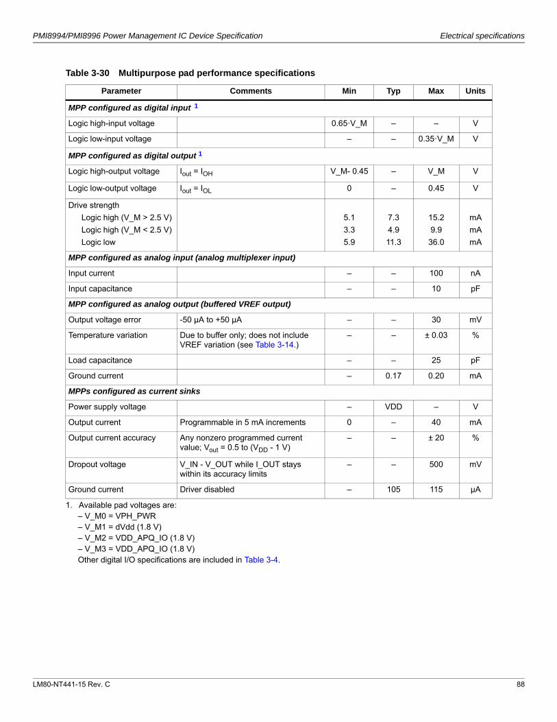
LM80-NT441-15 Rev. C 88
PMI8994/PMI8996 Power Management IC Device Specification Electrical specifications
Table 3-30 Multipurpose pad performance specifications
Parameter Comments Min Typ Max Units
MPP configured as digital input11
Logic high-input voltage 0.65·V_M – – V
Logic low-input voltage – – 0.35·V_M V
MPP configured as digital output 1
Logic high-output voltage Iout = IOH V_M- 0.45 – V_M V
Logic low-output voltage Iout = IOL 0 – 0.45 V
Drive strength
Logic high (V_M > 2.5 V)
Logic high (V_M < 2.5 V)
Logic low
5.1
3.3
5.9
7.3
4.9
11.3
15.2
9.9
36.0
mA
mA
mA
MPP configured as analog input (analog multiplexer input)
Input current – – 100 nA
Input capacitance – – 10 pF
MPP configured as analog output (buffered VREF output)
Output voltage error -50 µA to +50 µA – – 30 mV
Temperature variation Due to buffer only; does not include VREF variation (see Table 3-14.)
– – ± 0.03 %
Load capacitance – – 25 pF
Ground current – 0.17 0.20 mA
MPPs configured as current sinks
Power supply voltage – VDD – V
Output current Programmable in 5 mA increments 0 – 40 mA
Output current accuracy Any nonzero programmed current value; Vout = 0.5 to (VDD - 1 V)
– – ± 20 %
Dropout voltage V_IN - V_OUT while I_OUT stays within its accuracy limits
– – 500 mV
Ground current Driver disabled – 105 115 µA
1. Available pad voltages are:– V_M0 = VPH_PWR– V_M1 = dVdd (1.8 V)– V_M2 = VDD_APQ_IO (1.8 V)– V_M3 = VDD_APQ_IO (1.8 V)Other digital I/O specifications are included in Table 3-4.

LM80-NT441-15 Rev. C 89
4 Mechanical information
4.1 Device physical dimensions
The PMI8994/PMI8996 is available in the 210 WLNSP that includes ground pads for improved grounding, mechanical strength, and thermal continuity. The 210 WLNSP has a 5.69 mm × 6.24 mm body with a maximum height of 0.55 mm. Pad 1 is located by an indicator mark on the top of the package. A simplified version of the 210 WLNSP outline drawing is shown in Figure 4-1.
Figure 4-1 210 WLNSP (5.69 × 6.24 × 0.55 mm) package outline drawing
NOTE: This is a simplified outline drawing.

LM80-NT441-15 Rev. C 90
PMI8994/PMI8996 Power Management IC Device Specification Mechanical information
4.2 Part marking
4.2.1 Specification-compliant devices
Figure 4-2 PMI8994/PMI8996 device marking (top view, not to scale)
Table 4-1 PMI8994/PMI8996 device marking line definitions
Line Marking Description
1 QUALCOMM QTI company name or logo
2 PMI899x QTI product name
x = 4 for PMI8994
x = 6 for PMI8996
3 PPI P = Product configuration code – see Table 4-2
PI = Program ID code – see Table 4-2
E Blank or random Additional content as necessary
4 XXXXXXXX XXXXXXXX = traceability information
5 FAYWWRR F = wafer fab source of supply code
F = H for GLOBALFOUNDRIES
A = assembly (ball drop) code
A = U for Amkor
A = K for SPIL
A = M for JCET StatsChipPac
Y = single-digit year code
WW = workweek (based upon calendar year)
RR = product revision – see Table 4-2
6 • TTT ## TTT = engineering trace code
## = 2-digit wafer number
Ball 1 identifier
Line 2
Line 3
P M I 8 9 9 x
X X X X X X X XF A Y W W R R
Line 1
P P I
Line 4
Line E
Q U A L C O M M
T T T # #Line 5
Line 6

LM80-NT441-15 Rev. C 91
PMI8994/PMI8996 Power Management IC Device Specification Mechanical information
4.3 Device ordering information
4.3.1 Specification-compliant devices
This device can be ordered using the identification code shown in Figure 4-3 and explained below.
Figure 4-3 Device identification code
Device ordering information details for all samples available to date are summarized in Table 4-2.
4.4 Device moisture-sensitivity level
Surface mount packages are susceptible to damage induced by absorbed moisture and high temperature. A package’s moisture-sensitivity level (MSL) indicates its ability to withstand exposure after it is removed from its shipment bag, while it’s on the factory floor awaiting PCB installation. A low MSL rating is better than a high rating; a low MSL device can be exposed on the factory floor longer than a high MSL device. All pertinent MSL ratings are summarized in Table 4-4.
Example
Device ID code
Symboldefinition
Productname
AAA-AAAA
Config code
P
Numberof pads
Package type
Shipping package
Product version
Sourcecode
ProgramID
CCC DDDDD EE RR S PI— — — — — —
PMI-8994 0 210 WLNSP TR 00 0 00— — — — — —
Table 4-2 Device identification code/ordering information details
PMIC variant P value RR value Hardware ID # S value11 PI value22
CS sample type
PMI8994 CS (WiPower) 0 05 v2.0 0 03
PMI8996 CS (WiPower) 0 01 v1.1 0 01
1. ‘S’ is the source configuration code that identifies all the qualified die fabrication source combinations available at the time a particular sample type were shipped. S values are defined in Table 4-3.
2. ‘PI’ is the Program ID code that identifies an IC’s specific OTP programming that distinguishes it from other versions or variants. Defined feature sets available at the time of this document’s release are:– 00 = DC_IN charging path defaults to WiPower charging. This requires WiPower interfacing signals.– 01 = DC_IN charging path defaults to 5 V/9 V generic charging input. Interfacing signals not required.
Table 4-3 Source configuration code
S value Die F value = H
0 BiCMOS Global Foundries
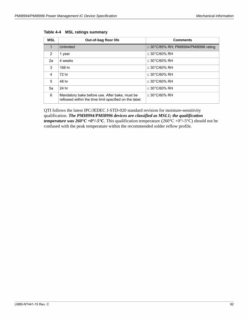
LM80-NT441-15 Rev. C 92
PMI8994/PMI8996 Power Management IC Device Specification Mechanical information
QTI follows the latest IPC/JEDEC J-STD-020 standard revision for moisture-sensitivity qualification. The PMI8994/PMI8996 devices are classified as MSL1; the qualification temperature was 260°C +0°/-5°C. This qualification temperature (260°C +0°/-5°C) should not be confused with the peak temperature within the recommended solder reflow profile.
Table 4-4 MSL ratings summary
MSL Out-of-bag floor life Comments
1 Unlimited 30°C/85% RH; PMI8994/PMI8996 rating
2 1 year 30°C/60% RH
2a 4 weeks 30°C/60% RH
3 168 hr 30°C/60% RH
4 72 hr 30°C/60% RH
5 48 hr 30°C/60% RH
5a 24 hr 30°C/60% RH
6 Mandatory bake before use. After bake, must be reflowed within the time limit specified on the label.
30°C/60% RH
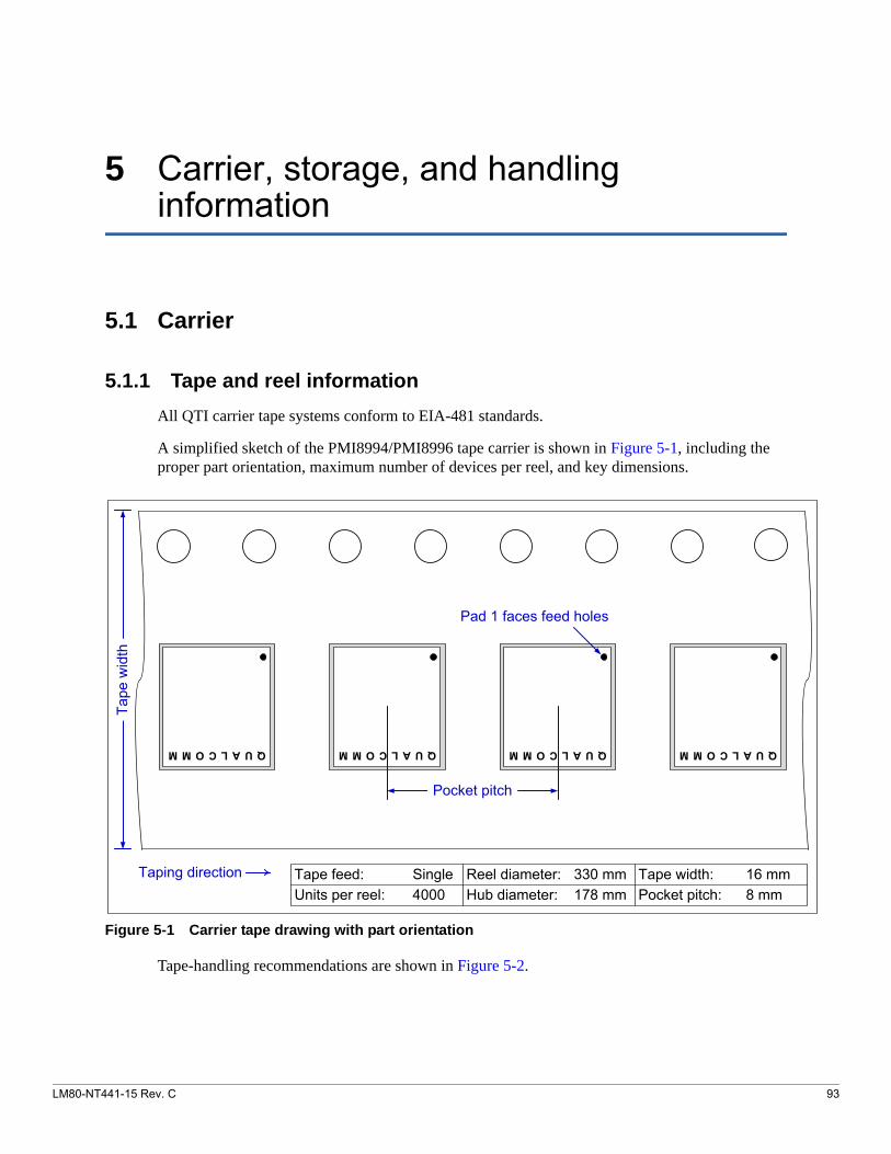
LM80-NT441-15 Rev. C 93
5 Carrier, storage, and handling information
5.1 Carrier
5.1.1 Tape and reel information
All QTI carrier tape systems conform to EIA-481 standards.
A simplified sketch of the PMI8994/PMI8996 tape carrier is shown in Figure 5-1, including the proper part orientation, maximum number of devices per reel, and key dimensions.
Figure 5-1 Carrier tape drawing with part orientation
Tape-handling recommendations are shown in Figure 5-2.
Taping direction
Tape
wid
th
Tape width:Pocket pitch:Units per reel:
Reel diameter:Hub diameter:
Tape feed: Single4000
330 mm178 mm
16 mm8 mm
QUALCOMM QUALCOMM QUALCOMM QUALCOMM
Pocket pitch
Pad 1 faces feed holes

LM80-NT441-15 Rev. C 94
PMI8994/PMI8996 Power Management IC Device Specification Carrier, storage, and handling information
Figure 5-2 Tape handling
5.2 Storage
5.2.1 Bagged storage conditions
PMI8994/PMI8996 devices delivered in tape and reel carriers must be stored in sealed, moisture barrier, antistatic bags.
5.2.2 Out-of-bag duration
The out-of-bag duration is the time a device can be on the factory floor before being installed onto a PCB. It is defined by the device MSL rating as discussed in Section 4.4.
5.3 Handling
Tape handling was discussed in Section 5.1.1. Other (IC-specific) handling guidelines are presented below.
Unlike traditional IC devices, the die within a wafer-level package is not protected by an overmold and there is no substrate; hence, these devices are relatively fragile.
NOTE: To avoid damage to the die due to improper handling, these recommendations should be followed:
• Do not use tweezers; a vacuum tip is recommended for handling the devices.
• Carefully select a pickup tool for use during the SMT process.
• Do not make contact with the device when reworking or tuning components located near the device.
5.3.1 Baking
Wafer-level packages such as the 210 WLNSP should not be baked.
Handle only at the edges

LM80-NT441-15 Rev. C 95
PMI8994/PMI8996 Power Management IC Device Specification Carrier, storage, and handling information
5.3.2 Electrostatic discharge
Electrostatic discharge (ESD) occurs naturally in laboratory and factory environments. An established high-voltage potential is always at risk of discharging to a lower potential. If this discharge path is through a semiconductor device, destructive damage may result.
ESD countermeasures and handling methods must be developed and used to control the factory environment at each manufacturing site.
QTI products must be handled according to the ESD Association standard: ANSI/ESD S20.20-1999, Protection of Electrical and Electronic Parts, Assemblies, and Equipment.
See Section 7.1 for the PMI8994/PMI8996 ESD ratings.

LM80-NT441-15 Rev. C 96
6 PCB mounting guidelines
6.1 RoHS compliance
The device is lead-free and RoHS-compliant. Its Sn/Ag/Cu solder balls use SAC405 composition. QTI defines its lead-free (or Pb-free) semiconductor products as having a maximum lead concentration of 1000 ppm (0.1% by weight) in raw (homogeneous) materials and end products.
6.2 SMT parameters
This section describes QTI board-level characterization process parameters. It is included to assist customers with their SMT process development; it is not intended to be a specification for their SMT processes.
6.2.1 Land pad and stencil design
The land-pattern and stencil recommendations presented in this section are based on QTI internal characterizations for lead-free solder pastes on an eight-layer PCB, built primarily to the specifications described in JEDEC JESD22-B111.
QTI recommends characterizing the land patterns according to each customer's processes, materials, equipment, stencil design, and reflow profile prior to PCB production. Optimizing the solder stencil pattern design and print process is critical to ensure print uniformity, decrease voiding, and increase board-level reliability.
General land-pattern guidelines:
Non-solder-mask-defined (NSMD) pads provide the best reliability.
Keep the solder-able area consistent for each pad, especially when mixing via-in-pad and non-via-in-pad in the same array.
Avoid large solder mask openings over ground planes.
Traces for external routing are recommended to be less than or equal to half the pad diameter, to ensure consistent solder-joint shapes.

LM80-NT441-15 Rev. C 97
PMI8994/PMI8996 Power Management IC Device Specification PCB mounting guidelines
One key parameter that should be evaluated is the ratio of aperture area to sidewall area, known as the area ratio (AR). QTI recommends square apertures for optimal solder-paste release. In this case, a simple equation can be used relating the side length of the aperture to the stencil thickness (as shown and explained in Figure 6-1). Larger area ratios enable better transfer of solder paste to the PCB, minimize defects, and ensure a more stable printing process. Inter-aperture spacing should be at least as thick as the stencil; otherwise, paste deposits may bridge.
Figure 6-1 Stencil printing aperture area ratio (AR)
Guidelines for an acceptable relationship between L and T are listed below, and are shown in Figure 6-2:
R = L/4T > 0.65 – best
0.60 R 0.65 – acceptable
R < 0.60 – not acceptable
Figure 6-2 Acceptable solder-paste geometries
T
AR = L / 4T
L
L
Aperture
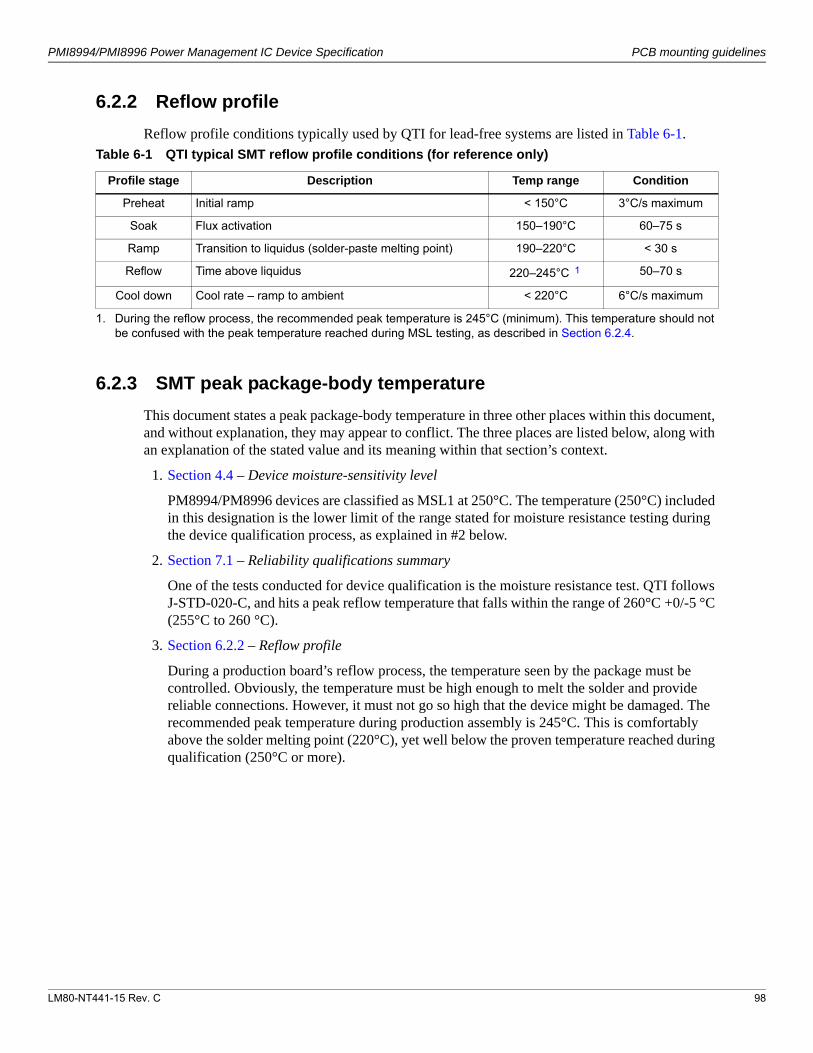
LM80-NT441-15 Rev. C 98
PMI8994/PMI8996 Power Management IC Device Specification PCB mounting guidelines
6.2.2 Reflow profile
Reflow profile conditions typically used by QTI for lead-free systems are listed in Table 6-1.
6.2.3 SMT peak package-body temperature
This document states a peak package-body temperature in three other places within this document, and without explanation, they may appear to conflict. The three places are listed below, along with an explanation of the stated value and its meaning within that section’s context.
1. Section 4.4 – Device moisture-sensitivity level
PM8994/PM8996 devices are classified as MSL1 at 250°C. The temperature (250°C) included in this designation is the lower limit of the range stated for moisture resistance testing during the device qualification process, as explained in #2 below.
2. Section 7.1 – Reliability qualifications summary
One of the tests conducted for device qualification is the moisture resistance test. QTI follows J-STD-020-C, and hits a peak reflow temperature that falls within the range of 260°C +0/-5 °C (255°C to 260 °C).
3. Section 6.2.2 – Reflow profile
During a production board’s reflow process, the temperature seen by the package must be controlled. Obviously, the temperature must be high enough to melt the solder and provide reliable connections. However, it must not go so high that the device might be damaged. The recommended peak temperature during production assembly is 245°C. This is comfortably above the solder melting point (220°C), yet well below the proven temperature reached during qualification (250°C or more).
Table 6-1 QTI typical SMT reflow profile conditions (for reference only)
Profile stage Description Temp range Condition
Preheat Initial ramp < 150°C 3°C/s maximum
Soak Flux activation 150–190°C 60–75 s
Ramp Transition to liquidus (solder-paste melting point) 190–220°C < 30 s
Reflow Time above liquidus 220–245°C11 50–70 s
Cool down Cool rate – ramp to ambient < 220°C 6°C/s maximum
1. During the reflow process, the recommended peak temperature is 245°C (minimum). This temperature should not be confused with the peak temperature reached during MSL testing, as described in Section 6.2.4.

LM80-NT441-15 Rev. C 99
PMI8994/PMI8996 Power Management IC Device Specification PCB mounting guidelines
6.2.4 SMT process verification
QTI recommends verification of the SMT process prior to high-volume board assembly, including:
Inline solder-paste deposition monitoring
Reflow-profile measurement and verification
Visual and x-ray inspection after soldering to confirm adequate alignment, solder voids, solder-ball shape, and solder bridging
Cross-section inspection of solder joints for wetting, solder-ball shape, and voiding

LM80-NT441-15 Rev. C 100
7 Part reliability
7.1 Reliability qualifications summary
Table 7-1 PMI8994 IC reliability evaluation
Tests, standards, and conditions11
1. Packaging tests do not appear here because the WLNSP has already been qualified prior to its use for the PMI8994 device.
Sample size
Result
Average failure rate (AFR) in FIT () failure in billion device-hours
HTOL: JESD22-A108-A
640 FIT = 179 at T500
Mean time to failure (MTTF) t = 1/ in million hours 640 5.59 Mhrs
ESD – human-body model (HBM) rating
JESD22-A114-F
3 ± 2000 V22
2. HBM ESD rating is 2000 V with the following minor exceptions:a) VSW_WLED to GND → 1 kV HBM ratingAll other pads meet 2000 V HBM ESD rating.
ESD – charge-device model (CDM) rating
JESD22-C101-D
3 ±500 V
Latch-up (I-test): EIA/JESD78C
Trigger current: ±100 mA; temperature: 85°C
3 ±100 mA
Latch-up (Vsupply overvoltage): EIA/JESD78C
Trigger voltage: stress at 1.5 × Vdd max per device specification; temperature: 85°C
3 6.6 V
Moisture resistance test (MRT): J-STD-020C
Reflow at 260 +0/-5°C
400 MSL1 pass
Temperature cycle: JESD22-A104-B
Temperature: -55°C to 125°C; number of cycles: 1000
Cycle rate: 2 cycles per hour (cph)
Preconditioning: JESD22-A113-F
MSL1, reflow at 260 +0/-5°C
400 Pass

LM80-NT441-15 Rev. C 101
PMI8994/PMI8996 Power Management IC Device Specification Part reliability
Table 7-2 PMI8996 IC reliability evaluation
Tests, standards, and conditions11
1. Packaging tests do not appear here because the WLNSP has already been qualified prior to its use for the PMI8994 device.
Sample size Result
Average failure rate (AFR) in FIT () failure in billion device-hours
HTOL: JESD22-A108-A
717 FIT = 110
Mean time to failure (MTTF) t = 1/ in million hours 717 9.09 Mhrs
ESD – Human-body model (HBM) rating
JESD22-A114-F
3 ±2000 V22
2. HBM ESD rating is 2000 V with the following minor exception: a. VSW_WLED to GND → 1 kV HBM ratingAll other pads meet the 2000 V HBM ESD rating.
ESD – Charged-device model (CDM) rating
JESD22-C101-D
3 500 V
Latch-up (I-test): EIA/JESD78A
Trigger current: ±100 mA; temperature: 85C3 100 mA
Latch-up (Vsupply overvoltage): EIA/JESD78A
Trigger voltage: Each VDD pad, stress at 1.5 × Vdd max per device specification; temperature: 85°C
3 6.6 V
Moisture resistance test (MRT): J-STD-020C
Reflow at 260 +0/-5°C
400 Pass
Temperature cycle: JESD22-A104-B
Temperature: -55°C to 125°C; number of cycles: 1000
Cycle rate: 2 cycles per hour (cph)
Preconditioning: JESD22-A113-F
MSL1, reflow at 260 +0/-5°C
400 Pass
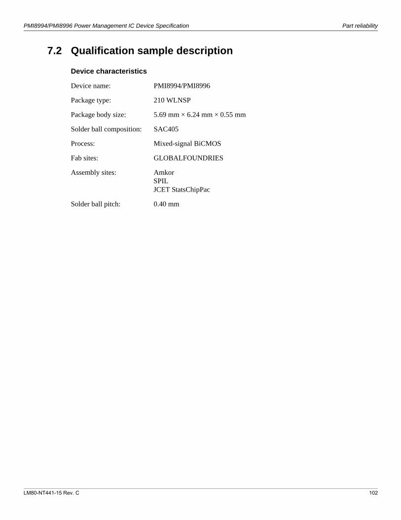
LM80-NT441-15 Rev. C 102
PMI8994/PMI8996 Power Management IC Device Specification Part reliability
7.2 Qualification sample description
Device characteristics
Device name: PMI8994/PMI8996
Package type: 210 WLNSP
Package body size: 5.69 mm × 6.24 mm × 0.55 mm
Solder ball composition: SAC405
Process: Mixed-signal BiCMOS
Fab sites: GLOBALFOUNDRIES
Assembly sites: AmkorSPILJCET StatsChipPac
Solder ball pitch: 0.40 mm

LM80-NT441-15 Rev. C 103
EXHIBIT 1
PLEASE READ THIS LICENSE AGREEMENT ("AGREEMENT") CAREFULLY. THIS AGREEMENT IS A BINDING LEGAL AGREEMENT ENTERED INTO BY AND BETWEEN YOU (OR IF YOU ARE ENTERING INTO THIS AGREEMENT ON BEHALF OF AN ENTITY, THEN THE ENTITY THAT YOU REPRESENT) AND QUALCOMM TECHNOLOGIES, INC. ("QTI" "WE" "OUR" OR "US"). THIS IS THE AGREEMENT THAT APPLIES TO YOUR USE OF THE DESIGNATED AND/OR ATTACHED DOCUMENTATION AND ANY UPDATES OR IMPROVEMENTS THEREOF (COLLECTIVELY, "MATERIALS"). BY USING, ACCESSING, DOWNLOADING OR COMPLETING THE INSTALLATION OF THE MATERIALS, YOU ARE ACCEPTING THIS AGREEMENT AND YOU AGREE TO BE BOUND BY ITS TERMS AND CONDITIONS. IF YOU DO NOT AGREE TO THESE TERMS, QTI IS UNWILLING TO AND DOES NOT LICENSE THE MATERIALS TO YOU. IF YOU DO NOT AGREE TO THESE TERMS YOU MUST DISCONTINUE AND YOU MAY NOT USE THE MATERIALS OR RETAIN ANY COPIES OF THE MATERIALS. ANY USE OR POSSESSION OF THE MATERIALS BY YOU IS SUBJECT TO THE TERMS AND CONDITIONS SET FORTH IN THIS AGREEMENT.
1.1 License. Subject to the terms and conditions of this Agreement, including, without limitation, the restrictions, conditions, limitations and exclusions set forth in this Agreement, Qualcomm Technologies, Inc. ("QTI") hereby grants to you a nonexclusive, limited license under QTI's copyrights to use the attached Materials; and to reproduce and redistribute a reasonable number of copies of the Materials. You may not use Qualcomm Technologies or its affiliates or subsidiaries name, logo or trademarks; and copyright, trademark, patent and any other notices that appear on the Materials may not be removed or obscured. QTI shall be free to use suggestions, feedback or other information received from You, without obligation of any kind to You. QTI may immediately terminate this Agreement upon your breach. Upon termination of this Agreement, Sections 1.2-4 shall survive.
1.2 Indemnification. You agree to indemnify and hold harmless QTI and its officers, directors, employees and successors and assigns against any and all third party claims, demands, causes of action, losses, liabilities, damages, costs and expenses, incurred by QTI (including but not limited to costs of defense, investigation and reasonable attorney's fees) arising out of, resulting from or related to: (i) any breach of this Agreement by You; and (ii) your acts, omissions, products and services. If requested by QTI, You agree to defend QTI in connection with any third party claims, demands, or causes of action resulting from, arising out of or in connection with any of the foregoing.
1.3 Ownership. QTI (or its licensors) shall retain title and all ownership rights in and to the Materials and all copies thereof, and nothing herein shall be deemed to grant any right to You under any of QTI's or its affiliates' patents. You shall not subject the Materials to any third party license terms (e.g., open source license terms). You shall not use the Materials for the purpose of identifying or providing evidence to support any potential patent infringement claim against QTI, its affiliates, or any of QTI's or QTI's affiliates' suppliers and/or direct or indirect customers. QTI hereby reserves all rights not expressly granted herein.
1.4 WARRANTY DISCLAIMER. YOU EXPRESSLY ACKNOWLEDGE AND AGREE THAT THE USE OF THE MATERIALS IS AT YOUR SOLE RISK. THE MATERIALS AND TECHNICAL SUPPORT, IF ANY, ARE PROVIDED "AS IS" AND WITHOUT WARRANTY OF ANY KIND, WHETHER EXPRESS OR IMPLIED. QTI ITS LICENSORS AND AFFILIATES MAKE NO WARRANTIES, EXPRESS OR IMPLIED, WITH RESPECT TO THE MATERIALS OR ANY OTHER INFORMATION OR DOCUMENTATION PROVIDED UNDER THIS AGREEMENT, INCLUDING BUT NOT LIMITED TO ANY WARRANTY OF MERCHANTABILITY OR FITNESS FOR A PARTICULAR PURPOSE OR AGAINST INFRINGEMENT, OR ANY EXPRESS OR IMPLIED WARRANTY ARISING OUT OF TRADE USAGE OR OUT OF A COURSE OF DEALING OR COURSE OF PERFORMANCE. NOTHING CONTAINED IN THIS AGREEMENT SHALL BE CONSTRUED AS (I) A WARRANTY OR REPRESENTATION BY QTI, ITS LICENSORS OR AFFILIATES AS TO THE VALIDITY OR SCOPE OF ANY PATENT, COPYRIGHT OR OTHER INTELLECTUAL PROPERTY RIGHT OR (II) A WARRANTY OR REPRESENTATION BY QTI THAT ANY MANUFACTURE OR USE WILL BE FREE FROM INFRINGEMENT OF PATENTS, COPYRIGHTS OR OTHER INTELLECTUAL PROPERTY RIGHTS OF OTHERS, AND IT SHALL BE THE SOLE RESPONSIBILITY OF YOU TO MAKE SUCH DETERMINATION AS IS NECESSARY WITH RESPECT TO THE ACQUISITION OF LICENSES UNDER PATENTS AND OTHER INTELLECTUAL PROPERTY OF THIRD PARTIES.
1.5 LIMITATION OF LIABILITY. IN NO EVENT SHALL QTI, QTI'S AFFILIATES OR ITS LICENSORS BE LIABLE TO YOU FOR ANY INCIDENTAL, CONSEQUENTIAL OR SPECIAL DAMAGES, INCLUDING BUT NOT LIMITED TO ANY LOST PROFITS, LOST SAVINGS, OR OTHER INCIDENTAL DAMAGES, ARISING OUT OF THE USE OR INABILITY TO USE, OR THE DELIVERY OR FAILURE TO DELIVER, ANY OF THE MATERIALS, OR ANY BREACH OF ANY OBLIGATION UNDER THIS AGREEMENT, EVEN IF QTI HAS BEEN ADVISED OF THE POSSIBILITY OF SUCH DAMAGES. THE FOREGOING LIMITATION OF LIABILITY SHALL REMAIN IN FULL FORCE AND EFFECT REGARDLESS OF WHETHER YOUR REMEDIES HEREUNDER ARE DETERMINED TO HAVE FAILED OF THEIR ESSENTIAL PURPOSE. THE ENTIRE LIABILITY OF QTI, QTI's AFFILIATES AND ITS LICENSORS, AND THE SOLE AND EXCLUSIVE REMEDY OF YOU, FOR ANY CLAIM OR CAUSE OF ACTION ARISING HEREUNDER (WHETHER IN CONTRACT, TORT, OR OTHERWISE) SHALL NOT EXCEED US$10.
2. COMPLIANCE WITH LAWS; APPLICABLE LAW.
Any litigation or other dispute resolution between You and Us arising out of or relating to this Agreement, or Your relationship with Us will take place in the Southern District of California, and You and QTI hereby consent to the personal jurisdiction of and exclusive venue in the state and federal courts within that District with respect any such litigation or dispute resolution. This Agreement will be governed by and construed in accordance with the laws of the United States and the State of California, except that body of California law concerning conflicts of law. This Agreement shall not be governed by the United Nations Convention on Contracts for the International Sale of Goods, the application of which is expressly excluded.
3. CONTRACTING PARTIES. If the Materials are downloaded on any computer owned by a corporation or other legal entity, then this Agreement is formed by and between QTI and such entity. The individual accepting the terms of this Agreement represents and warrants to QTI that they have the authority to bind such entity to the terms and conditions of this Agreement.
4. MISCELLANEOUS PROVISIONS. This Agreement, together with all exhibits attached hereto, which are incorporated herein by this reference, constitutes the entire agreement between QTI and You and supersedes all prior negotiations, representations and agreements between the parties with respect to the subject matter hereof. No addition or modification of this Agreement shall be effective unless made in writing and signed by the respective representatives of QTI and You. The restrictions, limitations, exclusions and conditions set forth in this Agreement shall apply even if QTI or any of its affiliates becomes aware of or fails to act in a manner to address any violation or failure to comply therewith. You hereby acknowledge and agree that the restrictions, limitations, conditions and exclusions imposed in this Agreement on the rights granted in this Agreement are not a derogation of the benefits of such rights. You further acknowledges that, in the absence of such restrictions, limitations, conditions and exclusions, QTI would not have entered into this Agreement with You. Each party shall be responsible for and shall bear its own expenses in connection with this Agreement. If any of the provisions of this Agreement are determined to be invalid, illegal, or otherwise unenforceable, the remaining provisions shall remain in full force and effect. This Agreement is entered into solely in the English language, and if for any reason any other language version is prepared by any party, it shall be solely for convenience and the English version shall govern and control all aspects. If You are located in the province of Quebec, Canada, the following applies: The Parties hereby confirm they have requested this Agreement and all related documents be prepared in English.
Related Documents