12824 DOI: 10.1021/la100399t Langmuir 2010, 26(15), 12824–12831 Published on Web 07/07/2010 pubs.acs.org/Langmuir © 2010 American Chemical Society Platinum-Doped CeO 2 Thin Film Catalysts Prepared by Magnetron Sputtering V. Matolı´n,* ,† I. Matolı´nov a, † M. V aclavu˚, † I. Khalakhan, † M. Vorokhta, † R. Fiala, † I. Pi s, †,# Z. Sofer, ‡ J. Poltierov a-Vejpravov a, § T. Mori, ^ V. Potin, ) H. Yoshikawa, # S. Ueda, # and K. Kobayashi # † Charles University, Faculty of Mathematics and Physics, Department of Surface and Plasma Science V Hole sovi ck ach 2, 18000 Prague 8, Czech Republic, ‡ Institute of Chemical Technology Prague, Deparment of Inorganic Chemistry, Technick a 5, 166 28 Prague 6, Czech Republic, § Charles University, Faculty of Mathematics and Physics, Department of Condensed Matter Physics, Ke Karlovu 5, 121 16 Praha 2, Czech Republic, ^ Ecomaterials Center, National Institute for Material Science, Namiki, Tsukuba, 305-0044, Japan, ) ICB - Laboratoire Interdisciplinaire Carnot de Bourgogne, UMR 5209 CNRS, Universit e de Bourgogne, 21078 Dijon CEDEX, France, and # NIMS Beamline Station at SPring-8, National Institute for Materials Science, Sayo, Hyogo 679-5148, Japan Received January 27, 2010. Revised Manuscript Received June 11, 2010 The interaction of Pt with CeO 2 layers was investigated by using photoelectron spectroscopy. The 30 nm thick Pt doped CeO 2 layers were deposited simultaneously by rf-magnetron sputtering on a Si(001) substrate, multiwall carbon nanotubes (CNTs) supported by a carbon diffusion layer of a polymer membrane fuel cell and on CNTs grown on the silicon wafer by the CVD technique. The synchrotron radiation X-ray photoelectron spectra showed the formation of cerium oxide with completely ionized Pt 2þ,4þ species, and with the Pt 2þ /Pt 4þ ratio strongly dependent on the substrate. The TEM and XRD study showed the Pt 2þ /Pt 4þ ratio is dependent on the film structure. 1. Introduction Pt-oxide anode materials such as Pt-RuO 2 , 1 Pt-SnO 2 , 2 and Pt-WO 3 3 have been reported as active catalysts for fuel cell applications. Recently, anode properties of Pt-CeO 2 have been investigated for the development of proton exchange membrane fuel cells (PEMFC). 4-6 Ionic Pt dispersed on a CeO 2 crystallite surface by the combus- tion method has been found to form active adsorption Pt 2þ,4þ sites which led to higher CO þ NO and CO þ O 2 reaction rates. 7,8 Pt ions incorporated in a CeO 2 matrix mostly in þ2 oxidation state enhance hydrogen molecule dissociation to protonic hydro- gen and increase hydrogen storage capacity of the catalyst. 8,9 Carbon nanotubes (CNTs) exhibit high electrical conductivity and excellent corrosion resistances. A CNT supported PtRu anode catalyst for direct methanol FC applications has been successfully tested, 10-14 also Pt coating of the CNT in form of supported nanoparticles was reported. 15-24 Zhang et al. used cerium oxide coated CNTs as a template for preparation of highly reactive CeO 2 nanotubes for CO oxidation. 25 Ceria decorated CNTs were also described by others as a promising novel catalyst. 26,27 Cerium oxide can be deposited by rf sputtering from a CeO 2 target. Variety of ceria based compounds can be prepared, e.g. Sn-CeO 2 , 28 by combining CeO 2 with other target materials. In this study we report electron microscopy, hard X-ray photo- electron spectroscopy (HAXPES) and X-ray diffraction (XRD) study of CNT coating by the Pt-CeO 2 catalyst by using simulta- neous magnetron sputtering of platinum and cerium oxide. This technique permits to prepare oxide layers continuously doped with *Corresponding author. E-mail: [email protected].. (1) Katayama, A. J. Phys. Chem. 1980, 84, 376–381. (2) Shen, P. K.; Tseung, A. C. C. J. Electrochem. Soc. 1994, 141, 3082–3090. (3) Rajeswari, J.; Viswanathan, B.; Varadarajan, T. K. Mater. Chem. Phys. 2007, 106, 168–174. (4) Xu, C. W.; Zeng, R.; Shen, P. K.; Wei, Z. D. Electrochim. Acta 2005, 51, 1031–1035. (5) Campos, C. L.; Roldan, C.; Aponte, M.; Ishikawa, Y.; Cabrera, C. R. J. Electroanal. Chem. 2005, 581, 206–215. (6) Takahashi, M.; Mori, T.; Ye, F.; Vinu, A.; Kobayashi, H.; Drennan, J. J. Am. Ceram. Soc. 2007, 90, 1291–1294. (7) Bera, P.; Patil, K. C.; Jayaram, V.; Subbanna, G. N.; Hedge, M. S. J. Catal. 2000, 196, 293–301. (8) Bera, P.; Gayen, A.; Hedge, M. S.; Lalla, N. P.; Spadaro, L.; Frusteri, F.; Arean, F. J. Phys. Chem. B 2003, 107, 6122–6130. (9) Dutta, G.; Waghmare, U. V.; Baidya, T.; Hedge, M. S. Chem. Mater. 2007, 19, 6430–6436. (10) Hsu, N. Y.; Chien, C. C.; Jeng, K. T. Appl. Catal., B 2008, 84, 196–203. (11) Liu, Z. L.; Ling, X. Y.; Guo, B.; Hong, L.; Lee, J. Y. J. Power Sources 2007, 167, 272–280. (12) Yang, C. W.; Wang, D. L.; Hu, X. G.; Dai, C. S.; Zhang, L. J. Alloys Compd. 2008, 448, 109–115. (13) An, G. M.; Yu, P.; Mao, L. Q.; Sun, Z. Y.; Liu, Z. M.; Miao, S. D.; Miao, Z. J.; Ding, K. L. Carbon 2007, 45, 536–542. (14) Liang, Y. M.; Zhang, H. M.; Yi, B. L.; Zhang, Z. H.; Tan, Z. C. Carbon 2005, 43, 3144–3152. (15) Kim, S.; Park, S. J. Anal. Chim. Acta 2008, 619, 43–48. (16) Lin, Y. H.; Cui, X. L.; Yen, C.; Wai, C. M. J. Phys. Chem. B 2005, 109, 14410–14415. (17) Liu, Z. L.; Lin, X. H.; Lee, J. Y.; Zhang, W.; Han, M.; Gan, L. M. Langmuir 2002, 18, 4054–4060. (18) Hull, R. V.; Li, L.; Xing, Y. C.; Chusuei, C. C. Chem. Mater. 2006, 18, 1780–1788. (19) Saha, M. S.; Li, R. Y.; Sun, X. H. J. Power Sources 2008, 177, 314–322. (20) Shao, Y. Y.; Yin, G. P.; Wang, H. H.; Gao, Y. Z.; Shi, P. F. J. Power Sources 2006, 161, 47–53. (21) Wu, G.; Xu, B. Q. J. Power Sources 2007, 174, 148–158. (22) Kim, Y. T.; Mitani, T. J. Catal. 2006, 238, 394–401. (23) Tong, H.; Li, H. L.; Zhang, X. G. Carbon 2007, 45, 2424–2432. (24) Li, W. Z.; Liang, C. H.; Qiu, J. S.; Zhou, W. J.; Han, H. M.; Wei, Z. B.; Sun, G. Q.; Xin, Q. Carbon 2002, 40, 791–794. (25) Zhang, D. S.; Pan, C. S.; Shi, L. Y.; Huang, L.; Fang, J. H.; Fu, H. X. Microporous Mesoporous Mater. 2009, 117, 193–200. (26) Kang, J. L.; Li, J. J.; Du, X. W.; Shi, C. S.; Zhao, N. Q.; Hu, R. X.; Nash, P. Mater. Lett. 2009, 63, 182–184. (27) Sun, Z. Y.; Zhang, X. R.; Han, B. X.; Wu, Y. Y.; An, G. M.; Liu, Z. M.; Miao, S. D.; Miao, Z. J. Carbon 2007, 45, 2589–2596. (28) Masek, K.; Vaclavu, M.; Babor, P.; Matolin, V. Appl. Surf. Sci. 2009, 255, 6656–6660.

Welcome message from author
This document is posted to help you gain knowledge. Please leave a comment to let me know what you think about it! Share it to your friends and learn new things together.
Transcript

12824 DOI: 10.1021/la100399t Langmuir 2010, 26(15), 12824–12831Published on Web 07/07/2010
pubs.acs.org/Langmuir
© 2010 American Chemical Society
Platinum-Doped CeO2 Thin Film Catalysts Prepared
by Magnetron Sputtering
V. Matolın,*,† I. Matolınov�a,† M. V�aclavu,† I. Khalakhan,† M. Vorokhta,† R. Fiala,†
I. Pi�s,†,# Z. Sofer,‡ J. Poltierov�a-Vejpravov�a,§ T. Mori,^ V. Potin, )
H. Yoshikawa,# S. Ueda,# and K. Kobayashi#
†Charles University, Faculty of Mathematics and Physics, Department of Surface and Plasma Science VHole�sovi�ck�ach 2, 18000 Prague 8, Czech Republic, ‡Institute of Chemical Technology Prague,
Deparment of Inorganic Chemistry, Technick�a 5, 166 28 Prague 6, Czech Republic, §Charles University,Faculty of Mathematics and Physics, Department of Condensed Matter Physics, Ke Karlovu 5, 121 16 Praha 2,Czech Republic, ^Ecomaterials Center, National Institute for Material Science, Namiki, Tsukuba, 305-0044,Japan, )ICB - Laboratoire Interdisciplinaire Carnot de Bourgogne, UMR5209CNRS,Universit�e de Bourgogne,21078 Dijon CEDEX, France, and #NIMS Beamline Station at SPring-8, National Institute for Materials
Science, Sayo, Hyogo 679-5148, Japan
Received January 27, 2010. Revised Manuscript Received June 11, 2010
The interaction of Pt with CeO2 layers was investigated by using photoelectron spectroscopy. The 30 nm thick Pt dopedCeO2 layerswere deposited simultaneously by rf-magnetron sputtering on a Si(001) substrate,multiwall carbon nanotubes(CNTs) supported by a carbon diffusion layer of a polymermembrane fuel cell and onCNTs grown on the siliconwafer bythe CVD technique. The synchrotron radiation X-ray photoelectron spectra showed the formation of cerium oxide withcompletely ionized Pt2þ,4þ species, and with the Pt2þ/Pt4þ ratio strongly dependent on the substrate. The TEM andXRDstudy showed the Pt2þ/Pt4þ ratio is dependent on the film structure.
1. Introduction
Pt-oxide anode materials such as Pt-RuO2,1 Pt-SnO2,
2 andPt-WO3
3 have been reported as active catalysts for fuel cellapplications. Recently, anode properties of Pt-CeO2 have beeninvestigated for the development of proton exchange membranefuel cells (PEMFC).4-6
Ionic Pt dispersed on a CeO2 crystallite surface by the combus-tion method has been found to form active adsorption Pt2þ,4þ
sites which led to higher COþNOandCOþO2 reaction rates.7,8
Pt ions incorporated in a CeO2 matrix mostly in þ2 oxidationstate enhance hydrogen molecule dissociation to protonic hydro-gen and increase hydrogen storage capacity of the catalyst.8,9
Carbon nanotubes (CNTs) exhibit high electrical conductivityand excellent corrosion resistances. ACNT supported PtRu anode
catalyst for direct methanol FC applications has been successfullytested,10-14 also Pt coating of the CNT in form of supportednanoparticles was reported.15-24 Zhang et al. used cerium oxidecoatedCNTs as a template for preparation of highly reactive CeO2
nanotubes for CO oxidation.25 Ceria decorated CNTs were alsodescribedbyothers as apromising novel catalyst.26,27Ceriumoxidecan be deposited by rf sputtering from a CeO2 target. Variety ofceria based compounds can be prepared, e.g. Sn-CeO2,
28 bycombining CeO2 with other target materials.
In this study we report electron microscopy, hard X-ray photo-electron spectroscopy (HAXPES) and X-ray diffraction (XRD)study of CNT coating by the Pt-CeO2 catalyst by using simulta-neous magnetron sputtering of platinum and cerium oxide. Thistechnique permits to prepare oxide layers continuously doped with
*Corresponding author. E-mail: [email protected]..(1) Katayama, A. J. Phys. Chem. 1980, 84, 376–381.(2) Shen, P. K.; Tseung, A. C. C. J. Electrochem. Soc. 1994, 141, 3082–3090.(3) Rajeswari, J.; Viswanathan, B.; Varadarajan, T. K. Mater. Chem. Phys.
2007, 106, 168–174.(4) Xu, C. W.; Zeng, R.; Shen, P. K.; Wei, Z. D. Electrochim. Acta 2005, 51,
1031–1035.(5) Campos, C. L.; Roldan, C.; Aponte, M.; Ishikawa, Y.; Cabrera, C. R.
J. Electroanal. Chem. 2005, 581, 206–215.(6) Takahashi, M.; Mori, T.; Ye, F.; Vinu, A.; Kobayashi, H.; Drennan, J.
J. Am. Ceram. Soc. 2007, 90, 1291–1294.(7) Bera, P.; Patil, K. C.; Jayaram, V.; Subbanna, G. N.; Hedge, M. S. J. Catal.
2000, 196, 293–301.(8) Bera, P.; Gayen, A.; Hedge, M. S.; Lalla, N. P.; Spadaro, L.; Frusteri, F.;
Arean, F. J. Phys. Chem. B 2003, 107, 6122–6130.(9) Dutta, G.; Waghmare, U. V.; Baidya, T.; Hedge, M. S. Chem. Mater. 2007,
19, 6430–6436.(10) Hsu, N. Y.; Chien, C. C.; Jeng, K. T. Appl. Catal., B 2008, 84, 196–203.(11) Liu, Z. L.; Ling, X. Y.; Guo, B.; Hong, L.; Lee, J. Y. J. Power Sources 2007,
167, 272–280.(12) Yang, C. W.; Wang, D. L.; Hu, X. G.; Dai, C. S.; Zhang, L. J. Alloys
Compd. 2008, 448, 109–115.(13) An, G. M.; Yu, P.; Mao, L. Q.; Sun, Z. Y.; Liu, Z. M.; Miao, S. D.; Miao,
Z. J.; Ding, K. L. Carbon 2007, 45, 536–542.
(14) Liang, Y. M.; Zhang, H. M.; Yi, B. L.; Zhang, Z. H.; Tan, Z. C. Carbon2005, 43, 3144–3152.
(15) Kim, S.; Park, S. J. Anal. Chim. Acta 2008, 619, 43–48.(16) Lin, Y. H.; Cui, X. L.; Yen, C.; Wai, C. M. J. Phys. Chem. B 2005, 109,
14410–14415.(17) Liu, Z. L.; Lin, X.H.; Lee, J. Y.; Zhang,W.; Han,M.; Gan, L.M.Langmuir
2002, 18, 4054–4060.(18) Hull, R. V.; Li, L.; Xing, Y. C.; Chusuei, C. C. Chem. Mater. 2006, 18,
1780–1788.(19) Saha, M. S.; Li, R. Y.; Sun, X. H. J. Power Sources 2008, 177, 314–322.(20) Shao, Y. Y.; Yin, G. P.; Wang, H. H.; Gao, Y. Z.; Shi, P. F. J. Power
Sources 2006, 161, 47–53.(21) Wu, G.; Xu, B. Q. J. Power Sources 2007, 174, 148–158.(22) Kim, Y. T.; Mitani, T. J. Catal. 2006, 238, 394–401.(23) Tong, H.; Li, H. L.; Zhang, X. G. Carbon 2007, 45, 2424–2432.(24) Li,W. Z.; Liang, C. H.; Qiu, J. S.; Zhou,W. J.; Han, H.M.;Wei, Z. B.; Sun,
G. Q.; Xin, Q. Carbon 2002, 40, 791–794.(25) Zhang, D. S.; Pan, C. S.; Shi, L. Y.; Huang, L.; Fang, J. H.; Fu, H. X.
Microporous Mesoporous Mater. 2009, 117, 193–200.(26) Kang, J. L.; Li, J. J.; Du, X.W.; Shi, C. S.; Zhao, N. Q.; Hu, R. X.; Nash, P.
Mater. Lett. 2009, 63, 182–184.(27) Sun, Z. Y.; Zhang, X. R.; Han, B. X.; Wu, Y. Y.; An, G. M.; Liu, Z. M.;
Miao, S. D.; Miao, Z. J. Carbon 2007, 45, 2589–2596.(28) Masek, K.; Vaclavu, M.; Babor, P.; Matolin, V. Appl. Surf. Sci. 2009, 255,
6656–6660.

DOI: 10.1021/la100399t 12825Langmuir 2010, 26(15), 12824–12831
Matolın et al. Article
Pt atoms during the growth. The Pt doped sputtered cerium oxidefilms contain high concentration of cationic platinum Pt2þ andPt4þ (nearly 100%) which opens the way for using such systems ashighly active thin film catalysts.29,30 Pt embedded in sputtered ceriafilms used as an anode material in a hydrogen PEMFC exhibitsvery high specific power (W/mg(Pt)) showing that such materialrepresents a promising alternative catalyst for FC applications.31
2. Experimental Section
Three types of catalyst substrates were investigated. Commer-cialmultiwall carbonnanotubes (MWCNTs) deposited on a gas dif-fusion layer (GDL) of thePEMFCand two reference substrates; aSi(001) wafer andCNTs grown on a Si(001) substrate by chemicalvapor deposition (CVD). The MWCNTs were purchased fromSigma-Aldrich andwere used as receivedwithout further purifica-tion. The nanotubes were dispersed in N,N-dimethylformamide(DMF) at a concentration of 1 mg/30 mL. Then the CNTs weredeposited onto a GDL (Alfa Aesar, Toray carbon paper, teflo-nated, TGP-60) substrate by sedimentation from the suspension.Typical timeofprecipitationwas 24h.TheGDLsubstrate areawas10 � 10 mm2 in order to fit the fuel cell size for the activity tests.
The CVD-CNTs on the Si wafer were grown by using Pt pre-cursor. APt ultrathin filmwas deposited on the substrate by usingDCmagnetron sputtering. The equivalent thickness of the depositof 0.5 nmwasdeterminedbyaquartzmicrobalance. The substratecovered by the Pt precursor was gradually heated up to 700 �Cwith temperature increase rate of 5 K/min and reactor purging bya mixture of H2 (60 sccm) and Ar (100 sccm). After reaching thefinal temperature theCNTswere grown in100 sccmofCH4mixedwith 400 sccm of Ar for 2 h. Then the reactor was cooled to roomtemperature in 600 sccm of Ar.
Nonreactive radio frequency (rf) magnetron sputtering wasused to deposit CeO2 andPt-CeO2 thin films on the Si(001) waferand the CNT substrates. CeO2 sputteringwas performed by usinga 2 in. CeO2 target at a distance of 90 mm from the Si substratewith rf power of 80 W giving a growth rate of the cerium oxidefilms of 1 nm/min. The Pt-CeO2 thin films were deposited fromacomposite target prepared by placing pieces of 1 mm thick and10 mm long Pt wire on the ceria target surface in the radial direc-tion.Depositionwas carriedout at roomtemperature inanAratmo-sphere by keeping the total pressure in the deposition chamberconstant at 4� 10-1 Pa, the growth rate obtained during the sput-tering was 1 nm/min. In this study we investigate the Pt dopedsamples with Pt concentration of 4.2 at% relative to a total amountof Ce and O atoms, determined by the laboratory X-ray photoelec-tron spectroscopy (XPS) with the Al KR source.
The HAXPES measurements32 were performed at the undu-lator beamline BL15XU of the SPring-8 synchrotron facility. TheX-raywasmonochromatized at 5956.5 eV by using a Si 333 channel-cut postmonochromator. The total energy resolutionΔE=280meVwas determined from the Fermi cutoff of a Au reference sample. AllHAXPES experiments were performed ex situ in ultrahigh vacuum(UHV) experimental chamber operating at base pressures around5� 10-9mbar, the spectrawere takenat thegrazingphoton incidenceand normal emission geometry.
Morphology of Pt-CeO2/CNTs was obtained by means ofscanning electronmicroscopy (SEM) by using a TESCAN -MIRAmicroscope at 30keVelectronbeamenergy.TEMobservationswerecarried out with a 200 kV JEOL 2100 (LaB6) microscope with aScherzer resolution of 0.25 nm. The images were recorded with an
online charged coupleddevice (CCD) cameraand theanalysesof theresults were performed using the Digital Micrograph software.
TheX-ray diffraction (XRD) patternswere recorded onX’pertPROMaterialResearchDiffractometer (PANalaytical) usingmono-chromatized Cu KR source. Because of the nm-range thickness ofthe films, surface-sensitive grazing incidence geometry was used.The incidence angleωwas fixed (typically at 1�), and the diffractionpatterns were recorded bymeans of asymmetric 2θ scans. The datawere analyzed using WinPlotr/FullProf software.33
The FC tests were performed by using a specially designedminiaturized fuel cell device.31Themembrane-electrode-assembly(MEA) was made by using Nafion 0.009 mm membrane sand-wiched by the catalyzed anode and cathode by hotpressing toform MEA of 1 cm2 (10 � 10 mm). MEA was clamped betweenstainless steel gas distributors sealed with silicon rubber. Moretechnical details of the cell implementation were introduced inref 31. The cathode electrode was made by carbon-supported Ptpowder (Alfa Aesar, Platinum, nominally 40% on carbon black)mixed with the Nafion solution (Alfa Aesar, Perfluorosulfonicacid-PTFE copolymer, 5% w/w solution) and deposited on theGDL.Loading of Pt in the cathode catalyst layer was 1.1mg/cm2.To evaluate cell performance pure humidificated hydrogen andair were used as fuel and oxidant under atmospheric pressure. Theflow rates of H2 and O2 were controlled at 30.0 mL/min.
3. Results
Electron Microscopy. High resolution SEM was used forinvestigation of surface morphology of coated MWCNTs andCVD grown CNTs. Detailed SEM image of the MWCNT/GDLsample coated by Pt-CeO2 film is presented in Figure 1. Thefigure inset shows clearly uniform character of well spread CNTdeposit suitable for preparation of large active surface catalyst.Outer diameter of the bare nanotubes, determined from the SEMimages (not shown), reveals average value around 100 nm.Lengthranged from5 to 10μm.Figure 2 shows theCNTs grownon the Sisubstrate byCVD.The bareCNTs exhibited diameter of 17 nm inaverage.Figure 2 shows theCNTs attached perpendicularly to thesubstrate forming a dense fur like overlayer. SEMstudy of a parti-ally removed CNT layer (upper panel) permitted to determineCNT length of 3-5 μm.
High-resolution TEM (HRTEM) was performed on all threetypes of the samples. Figure 3 shows image of a piece of thePt-CeO2 film detached from the Si substrate. The right panelpresents a low magnification image of the detached film. One candistinguish a columnar structure which is typical for sputteredthin films. The left panel shows a typical HRTEM image of the
Figure 1. SEM image of detail of coated Pt-CeO2 film coatedMWCNTs. Inset shows CNT arrangement.
(29) Fu, Q.; Saltsburg, H.; Flytzani-Stephanopoulos, M. Science 2003, 301,935–938.(30) Pierre, D.; Deng,W. L.; Flytzani-Stephanopoulos, M.Top. Catal. 2007, 46,
363–373.(31) Vaclavu, M.; Matolinova, I.; Myslivecek, J.; Fiala, R.; Matolin, V.
J. Electrochem. Soc. 2009, 156, B938–B942.(32) Kobayashi, K.; Yabashi, M.; Takata, Y.; Tokushima, T.; Shin, S.;
Tamasaku, K.; Miwa, D.; Ishikawa, T.; Nohira, H.; Hattori, T.; Sugita, Y.;Nakatsuka, O.; Sakai, A.; Zaima, S. Appl. Phys. Lett. 2003, 83, 1005.
(33) Roisnel, T.; Rodriguez-Carvajal, J. WinPLOTR: a Windows tool forpowder diffraction patterns analysis. In Matererial Science Forum, Proceedingsof the Seventh European Powder Diffraction Conference (EPDIC 7); Trans TechPublications: Switzerland, 2000; pp 118-123, http://www.ill.eu/sites/fullprof/.

12826 DOI: 10.1021/la100399t Langmuir 2010, 26(15), 12824–12831
Article Matolın et al.
polycrystalline film structure. Small crystals of 5-8 nm exhibitplane distance of 0.31 nm which corresponds to d111 plane dis-tance of CeO2. The structure labeled by the circle representstypical HRTEM image of the CeO2 with [110] zone axis.
The upper panel of Figure 4 showsTEM image of coated singleCNT, the tube diameter is indicated by a white arrow. TheHRTEM image of the sample detail is seen in the lower panelof Figure 4. The HRTEM micrograph reveals bright and darkdomains of different composition determined by energy disper-sive spectrometry (EDS). The atomic concentrations of carbon,oxygen, cerium and platinum are indicated in figure. The darkdomains indicate the sample regionwith the Pt richer compositionand show the plane distance of 0.23 nm, mainly. This structurecan be associated with interplanar distances observed in thePt2Ce, Pt5Ce alloy,
34,35 andmetallic Pt.36 Themeasured distancesin the bright domains corresponding to the (111) plane distances
of CeO2 are also shown in Figure 3. The same structures can beseen in the Pt-CeO2 coating of the MWCNTs, see Figure 5. Weshould note that EDS determined concentrations are obtainedusing a 5 nm size probe and represent a local probe analysis;therefore they cannot be used as an indication of an averagecompositionwhich is provided byXPS. In addition, the EDS spotanalysis has a destructive effect on oxide materials which can bedecomposed by the beam. Therefore, quantitative analysis is notalways reliable; however it can be easily used for determination ofconcentration variations.Photoelectron Spectroscopy. Chemical state and composi-
tion of the catalysts were investigated by hard X-ray photoelec-tron spectroscopy with photon energy of 5956 eV. The catalystsprepared by sputtering exhibit porous structure, as shown below,which causes that a large part of the active catalyst surface is
Figure 2. SEM image of the CVD grown CNTs on the Si wafer(upper) and of detail of coated CNT (bottom).
Figure 3. HRTEMof structure of the Pt-CeO2 film deposited onthe Si wafer (left) and TEM image of the film (right).
Figure 4. TEM image of the Pt-CeO2 film coated CVD-CNT(upper) andHRTEMdetail (bottom). Circles indicate zoneswherethe EDS analysis was performed.
Figure 5. TEMimage of the coatedMWCNT (inset) andHRTEMof the Pt-CeO2 film on MWCNT. Circle indicates zone where theEDS analysis was performed.
(34) Berner, U.; Schierbaum, K. D. Phys. Rev. B 2002, 65, 235404.(35) Tang, J.; Lawrence, J. M.; Hemminger, J. C. Phys. Rev. B 1993, 48, 15342.(36) Bernal, S.; Calvino, J. J.; Cauqui, M. A.; Gatica, J. M.; Cartes, C. L.; Omil,
J. A. P.; Pintado, J. M. Catal. Today 2003, 77, 385.
DOI: 10.1021/la100399t 12827Langmuir 2010, 26(15), 12824–12831
Matolın et al. Article
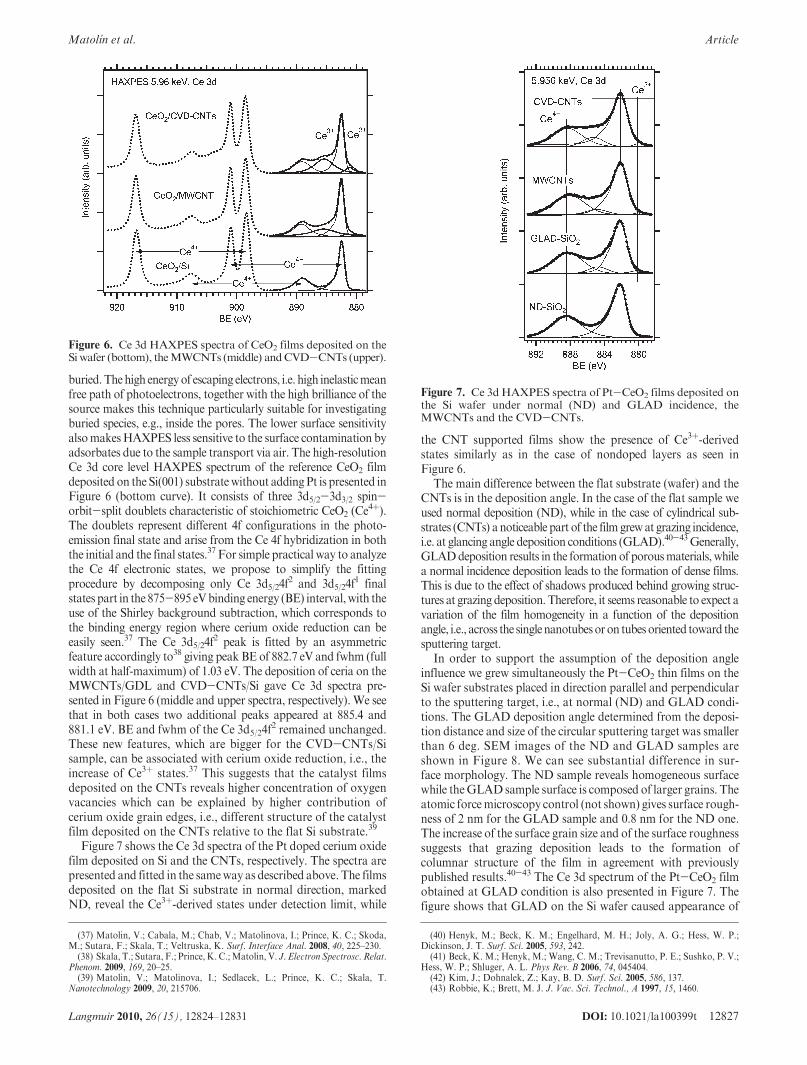
buried.Thehigh energyof escaping electrons, i.e. high inelasticmeanfree path of photoelectrons, together with the high brilliance of thesource makes this technique particularly suitable for investigatingburied species, e.g., inside the pores. The lower surface sensitivityalsomakesHAXPES less sensitive to the surface contamination byadsorbates due to the sample transport via air. The high-resolutionCe 3d core level HAXPES spectrum of the reference CeO2 filmdeposited on the Si(001) substratewithout addingPt is presented inFigure 6 (bottom curve). It consists of three 3d5/2-3d3/2 spin-orbit-split doublets characteristic of stoichiometric CeO2 (Ce
4þ).The doublets represent different 4f configurations in the photo-emission final state and arise from the Ce 4f hybridization in boththe initial and the final states.37 For simple practical way to analyzethe Ce 4f electronic states, we propose to simplify the fittingprocedure by decomposing only Ce 3d5/24f
2 and 3d5/24f1 final
states part in the 875-895 eVbinding energy (BE) interval,with theuse of the Shirley background subtraction, which corresponds tothe binding energy region where cerium oxide reduction can beeasily seen.37 The Ce 3d5/24f
2 peak is fitted by an asymmetricfeature accordingly to38 giving peak BE of 882.7 eV and fwhm (fullwidth at half-maximum) of 1.03 eV. The deposition of ceria on theMWCNTs/GDL and CVD-CNTs/Si gave Ce 3d spectra pre-sented in Figure 6 (middle and upper spectra, respectively). We seethat in both cases two additional peaks appeared at 885.4 and881.1 eV. BE and fwhm of the Ce 3d5/24f
2 remained unchanged.These new features, which are bigger for the CVD-CNTs/Sisample, can be associated with cerium oxide reduction, i.e., theincrease of Ce3þ states.37 This suggests that the catalyst filmsdeposited on the CNTs reveals higher concentration of oxygenvacancies which can be explained by higher contribution ofcerium oxide grain edges, i.e., different structure of the catalystfilm deposited on the CNTs relative to the flat Si substrate.39
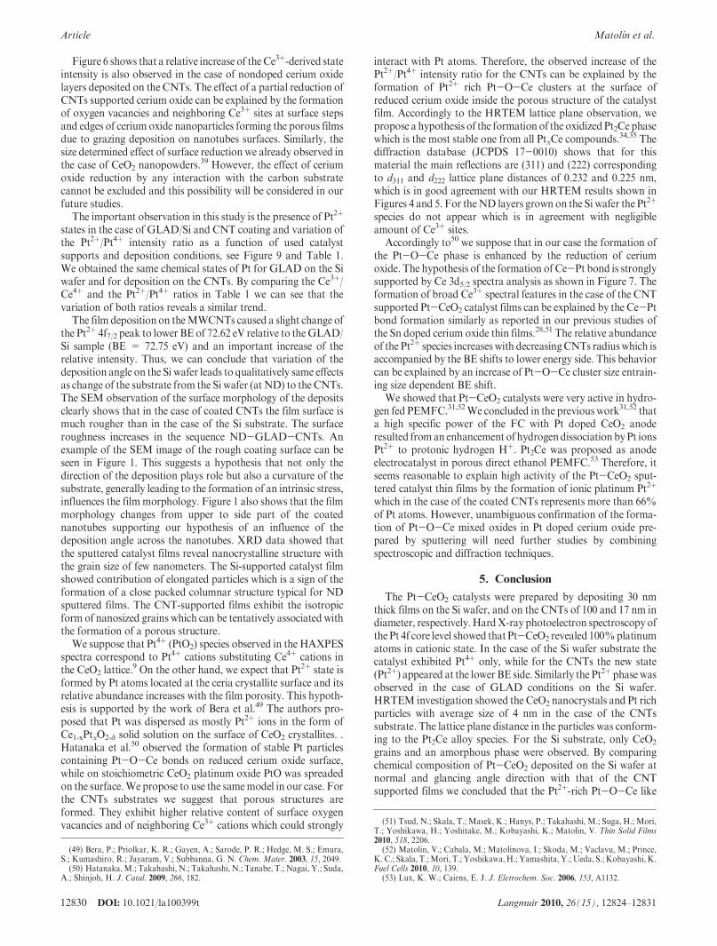
Figure 7 shows the Ce 3d spectra of the Pt doped cerium oxidefilm deposited on Si and the CNTs, respectively. The spectra arepresented and fitted in the sameway as described above. The filmsdeposited on the flat Si substrate in normal direction, markedND, reveal the Ce3þ-derived states under detection limit, while
the CNT supported films show the presence of Ce3þ-derivedstates similarly as in the case of nondoped layers as seen inFigure 6.
The main difference between the flat substrate (wafer) and theCNTs is in the deposition angle. In the case of the flat sample weused normal deposition (ND), while in the case of cylindrical sub-strates (CNTs) anoticeable part of the filmgrewat grazing incidence,i.e. at glancing angle deposition conditions (GLAD).40-43Generally,GLADdeposition results in the formation of porousmaterials, whilea normal incidence deposition leads to the formation of dense films.This is due to the effect of shadows produced behind growing struc-tures at grazing deposition. Therefore, it seems reasonable to expect avariation of the film homogeneity in a function of the depositionangle, i.e., across the singlenanotubesoron tubesoriented toward thesputtering target.
In order to support the assumption of the deposition angleinfluence we grew simultaneously the Pt-CeO2 thin films on theSi wafer substrates placed in direction parallel and perpendicularto the sputtering target, i.e., at normal (ND) and GLAD condi-tions. The GLAD deposition angle determined from the deposi-tion distance and size of the circular sputtering target was smallerthan 6 deg. SEM images of the ND and GLAD samples areshown in Figure 8. We can see substantial difference in sur-face morphology. The ND sample reveals homogeneous surfacewhile theGLADsample surface is composed of larger grains. Theatomic forcemicroscopy control (not shown) gives surface rough-ness of 2 nm for the GLAD sample and 0.8 nm for the ND one.The increase of the surface grain size and of the surface roughnesssuggests that grazing deposition leads to the formation ofcolumnar structure of the film in agreement with previouslypublished results.40-43 The Ce 3d spectrum of the Pt-CeO2 filmobtained at GLAD condition is also presented in Figure 7. Thefigure shows that GLAD on the Si wafer caused appearance of
Figure 6. Ce 3d HAXPES spectra of CeO2 films deposited on theSiwafer (bottom), theMWCNTs (middle) andCVD-CNTs (upper).
Figure 7. Ce 3dHAXPES spectra of Pt-CeO2 films deposited onthe Si wafer under normal (ND) and GLAD incidence, theMWCNTs and the CVD-CNTs.
(37) Matolin, V.; Cabala, M.; Chab, V.; Matolinova, I.; Prince, K. C.; Skoda,M.; Sutara, F.; Skala, T.; Veltruska, K. Surf. Interface Anal. 2008, 40, 225–230.(38) Skala, T.; Sutara, F.; Prince, K. C.;Matolin, V. J. Electron Spectrosc. Relat.
Phenom. 2009, 169, 20–25.(39) Matolin, V.; Matolinova, I.; Sedlacek, L.; Prince, K. C.; Skala, T.
Nanotechnology 2009, 20, 215706.
(40) Henyk, M.; Beck, K. M.; Engelhard, M. H.; Joly, A. G.; Hess, W. P.;Dickinson, J. T. Surf. Sci. 2005, 593, 242.
(41) Beck, K. M.; Henyk, M.; Wang, C. M.; Trevisanutto, P. E.; Sushko, P. V.;Hess, W. P.; Shluger, A. L. Phys Rev. B 2006, 74, 045404.
(42) Kim, J.; Dohnalek, Z.; Kay, B. D. Surf. Sci. 2005, 586, 137.(43) Robbie, K.; Brett, M. J. J. Vac. Sci. Technol., A 1997, 15, 1460.

12828 DOI: 10.1021/la100399t Langmuir 2010, 26(15), 12824–12831
Article Matolın et al.
Ce3þ sites which corresponded to a partial reduction of ceriumoxide giving similar spectral features as in the case of depositionon the CNTs.
To determine the Ce3þ/Ce4þ ratios for all the samples fromFigure 7, the Ce3þ 3d peak areas were calculated using the knownCe 3d5/2/3d3/2 peak area ratio of 1.18. The Ce
4þ3d area was deter-mined as a difference between the total area of the Ce 3d peak andthe Ce3þ 3d peak area. The ratios are presented in Table 1. Bycomparing Figures 6 and 7 we can see that the 3d5/24f
2 final stateof the Pt doped films are fitted by 0.9 eV broader peaks thanundoped films and the degree of reduction of cerium oxide increasesin order NDf GLADfMWCNTs f CVD-CNTs.
The Pt 4fHAXPES spectra are plotted in Figure 9. The spectrumof the ND film on the silicon wafer (see the bottom spectrum)exhibits a Pt 4f7/2-4f5/2 doublet at 74.3-77.6 eV corresponding toPt4þ.44 The CVD-CNTs/Si and the MWCNTs/GDL samplesreveal Pt4þ features and additional Pt2þ doublets at 72.5-75.8and 72.6-75.9 eV, respectively.29,45 GLAD on the Si wafer showsPt2þ 4f spectral features at 72.75-75.75 eV. The CVD-CNTssample shows in addition small Pt 4f7/2 contribution at 71.0 eV,which is assigned to the Pt0 state of the platinum particles used as aCVD precursor.
We checked the stability of samples under photon beamexposure. We found that the ND catalyst film on the Si waferrevealed only negligible changes with time of irradiation. On theother hand, the GLAD film as well as coated CNTs exhibitedvariations of relative intensity of peaks attributed to different
states ofPt observed as an increase of thePt2þ/Pt4þ peak area ratio.For this reason we started measurements of all Pt 4f spectra(Figure 9) immediately after positioning the beam on a “fresh”nonirradiated area (beam size on the sample is about 0.04� 3mm2)of the sample and we measured only one scan. Comparing thereduction speed and time required for the spectrum acquisition weconcluded that the Pt2þ/Pt4þ peak area ratio changes induced byirradiation damage during the measurements were below 5%.
The results presented in Figure 9 show that platinum atoms inthe ceria layers are fully ionic as we already reported.31 In addi-tion, Figure 9 clearly shows surprising results that the Pt2þ/Pt4þ
ratio and Pt2þ binding energy strongly depends on a type of thesupport (we note that the samples were prepared simultaneously).The Pt2þ/Pt4þ concentration ratios and Pt2þ 4f binding energiesare presented in Table 1.X-ray Diffraction Study. In parts a and b of Figure 10, we
present an example of the XRD pattern of Pt doped cerium oxidefilm deposited on Si (ND) and CVD-CNTs. The XRD patternsshow clearly peaks attributed to the fluorite-typeCeO2 phase. Theoutstanding difference between the diffraction line profiles isreflected by a larger asymmetry and width of the reflections incase of the films deposited on Si. Moreover, significant peakaround Q = 2.3 A-1 attributed to the Pt(111) reflection can bedetected in theCVD-CNTdeposited samples, and it correspondsto Pt particles deposited on the Si wafer for catalyzing the CVDgrowth. The critical interval, where the substrate scattering over-laps with the CeO2 diffraction lines was considered with lowpriority in the modeling procedure. The expected contribution ofthe CNTs was observed as a small broad peak atQ= 1.5 A-1 inFigure 10 a. The CNT contribution is negligible and does notinfluence any profile of the CeO2 phase, so it was treated asbackground in further analysis.
However, no characteristic CeO2 diffraction was observed inthe samples deposited on the MWCNT/GDL substrate. Diffrac-tion of theMWCNT/GDL substrate dominates in spite of the thinfilmgeometry of the experiment, because theCeO2,which clings onthe substrate surface, is mostly screened by its rugged structure.
The combined Rietveld and profile analysis was performedfor the samples deposited on the Si wafer and the CVD-CNTs.
Figure 8. SEM image of Pt-CeO2 films deposited on the Sisubstrate at (a) normal and (b) glancing angle deposition.
Table 1. Ce3þ/Ce4þ and Pt2þ/Pt4þConcentration Ratios and Pt2þ 4f
Binding Energies for Samples Prepared on Different Types
of the Support
substrate Ce3þ/Ce4þ Pt2þ/Pt4þ Pt2þ 4f7/2 BE (eV)
CVD CNTs 0.06 2.4 72.47MWCNTs/GDL 0.03 2.0 72.62Si wafer, GLAD 0.02 0.1 72.75Si wafer, ND 0 0
Figure 9. Pt 4f HAXPES spectra of Pt-CeO2 films deposited onthe Si wafer under normal (ND) and GLAD incidence, theMWCNTs and the CVD-CNTs.
(44) Tang, X.; Zhang, B.; Li, Y.; Xu, Y.; Xin, Q.; Shen,W. J.Mol. Catal. A 2005,235, 122.(45) Osterlund, L.; Kielbassa, S.; Werdinius, C.; Kasemo, B. J. Catal. 2003,
215, 94.

DOI: 10.1021/la100399t 12829Langmuir 2010, 26(15), 12824–12831
Matolın et al. Article
Both the instrumental and sample intrinsic profiles are supposedto be described by a convolution of Lorentzian and Gaussiancomponents. The pseudo-Voigt profile function46 is used tomimic the exact Voigt function and it includes the Finger’streatment of the axial divergence.47 The anisotropic size broad-ening along each reciprocal lattice vector is analyzed using theScherrer formula expressed as a linear combination of sphericalharmonics formulated for the m3m Laue class.48 The anisotropicsize is supposed to contribute to the Lorentzian component of thetotal Voigt function. The XRD patterns were first fitted using asingleCeO2 phase including the effect of isotropic size broadeningto the diffraction lines with admixture of isotropic strain. Theprofiles were not properly described; consequently anisotropicsize broadening was introduced for the CVD-CNT substrate.The apparent crystallite size was 4.7 nm with the minor sizeanisotropy contribution of 0.9 nm for theCNTs. In the case of theSi supported films (ND) we found two populations of ceriumoxide particles, 4.0 nm of negligible anisotropy and 6.3 nm oneswith the size anisotropy of 3.6 nm, i.e., elongated ones.Fuel Cell Test. The sample prepared by using GDL as a
support was suitable for the fuel cell test of the catalyst activity.The performance of the PEMFC with the Pt-CeO2 film coatedMWCNT/GDL used as anode was investigated for different temp-eratures in the interval 18 - 75 �C. The polarization V-I curvesobtained at 21 and 75 �C are shown in Figure 11 together with thepower density (PD) characteristics. We can see that at room temp-eratureweobtainedmaximumpower density PDmax=25mW/cm2.The best obtained result was PDmax = 38 mW/cm2 at 75 �C.This value corresponded to maximum specific power SPmax =42 W/mg(Pt) (calculated by using Pt loading of 0.9 μg/cm2).This result is similar to that of our previous results (35 W/mg(Pt))31 were we studied the PEMFC anode made of the samesputtered catalytic material on finer double wall CNTs depo-sited on the GDL by spin coating. The FC test confirmedexcellent catalytic properties of the Pt-CeO2 coated CNTscharacteristic by high performance at very low Pt loading.
4. Discussion
In the case of the catalyst film deposition on the CNTs orientedin parallel (MWCNTs) or in perpendicular (CVD-CNTs) relativeto the sputtering target surface, a noticeable part of the film growsat grazing incidence, i.e. at glancing angle deposition conditions(GLAD).40-43 Robbie and Bratt showed convincing example of
several materials grown at GLAD conditions giving three-dimen-sional columnar porous microstructures.43 Therefore, we expecta variation of the film morphology and porosity across the indivi-dual nanotubes oriented in parallel (MWCNTs) or perpendicular(CVD-CNTs) to the sputtering target. This hypothesis is supportedby comparison of HAXPES results obtained for the Pt-CeO2 thinfilms grown simultaneously on the Si wafer substrates placed in thedirection parallel and perpendicular to the sputtering target, i.e. atND and GLAD conditions. By comparing the Ce 3d spectra inFigure 7,we found thatGLADon theSiwafer and theCNTscausedthe appearance ofCe3þ-derived sites, i.e., partial reduction of ceriumoxide, while ND led to stoichiometric cerium oxide.
Figure 10. Comparison of the experimental data (open circles) and the final fits (solid lines) in the scattering vector (Q = 4π/λ(sin θ))representation. The vertical lines mark the Bragg positions of the CeO2 (red) and Pt (blue). The scattering contribution of the CNTs in thePt-CeO2/CVD CNTs sample (panel a) is depicted by the black arrow. The Bragg positions of the two CeO2 fractions in the Pt-CeO2/Sisample (panel b) are so close, that only a single set of the markers is shown for clarity.
Figure 11. Polarization and power density versus current densityusing hydrogen/air flow of the fuel cell with Pt-CeO2/MWCNT/GDL anode at 21 and 75 �C.
(46) Thompson, P.; Cox, D. E.; Hastings, J. B. J. Appl. Crystallogr. 1987, 20, 79.(47) Finger, L. W. J. Appl. Crystallogr. 1998, 31, 111.(48) Jarvinen, M. J. Appl. Crystallogr. 1993, 26, 527.
12830 DOI: 10.1021/la100399t Langmuir 2010, 26(15), 12824–12831
Article Matolın et al.
Figure 6 shows that a relative increase of theCe3þ-derived stateintensity is also observed in the case of nondoped cerium oxidelayers deposited on the CNTs. The effect of a partial reduction ofCNTs supported cerium oxide can be explained by the formationof oxygen vacancies and neighboring Ce3þ sites at surface stepsand edges of cerium oxide nanoparticles forming the porous filmsdue to grazing deposition on nanotubes surfaces. Similarly, thesize determined effect of surface reduction we already observed inthe case of CeO2 nanopowders.
39 However, the effect of ceriumoxide reduction by any interaction with the carbon substratecannot be excluded and this possibility will be considered in ourfuture studies.
The important observation in this study is the presence of Pt2þ
states in the case of GLAD/Si and CNT coating and variation ofthe Pt2þ/Pt4þ intensity ratio as a function of used catalystsupports and deposition conditions, see Figure 9 and Table 1.We obtained the same chemical states of Pt for GLAD on the Siwafer and for deposition on the CNTs. By comparing the Ce3þ/Ce4þ and the Pt2þ/Pt4þ ratios in Table 1 we can see that thevariation of both ratios reveals a similar trend.
The film deposition on theMWCNTs caused a slight change ofthe Pt2þ 4f7/2 peak to lower BE of 72.62 eV relative to theGLAD/Si sample (BE = 72.75 eV) and an important increase of therelative intensity. Thus, we can conclude that variation of thedeposition angle on the Si wafer leads to qualitatively same effectsas change of the substrate from the Si wafer (at ND) to the CNTs.The SEM observation of the surface morphology of the depositsclearly shows that in the case of coated CNTs the film surface ismuch rougher than in the case of the Si substrate. The surfaceroughness increases in the sequence ND-GLAD-CNTs. Anexample of the SEM image of the rough coating surface can beseen in Figure 1. This suggests a hypothesis that not only thedirection of the deposition plays role but also a curvature of thesubstrate, generally leading to the formation of an intrinsic stress,influences the filmmorphology. Figure 1 also shows that the filmmorphology changes from upper to side part of the coatednanotubes supporting our hypothesis of an influence of thedeposition angle across the nanotubes. XRD data showed thatthe sputtered catalyst films reveal nanocrystalline structure withthe grain size of few nanometers. The Si-supported catalyst filmshowed contribution of elongated particles which is a sign of theformation of a close packed columnar structure typical for NDsputtered films. The CNT-supported films exhibit the isotropicform of nanosized grains which can be tentatively associated withthe formation of a porous structure.
We suppose that Pt4þ (PtO2) species observed in the HAXPESspectra correspond to Pt4þ cations substituting Ce4þ cations inthe CeO2 lattice.
9 On the other hand, we expect that Pt2þ state isformed by Pt atoms located at the ceria crystallite surface and itsrelative abundance increases with the film porosity. This hypoth-esis is supported by the work of Bera et al.49 The authors pro-posed that Pt was dispersed as mostly Pt2þ ions in the form ofCe1-xPtxO2-δ solid solution on the surface of CeO2 crystallites. .Hatanaka et al.50 observed the formation of stable Pt particlescontaining Pt-O-Ce bonds on reduced cerium oxide surface,while on stoichiometric CeO2 platinum oxide PtO was spreadedon the surface.We propose to use the samemodel in our case. Forthe CNTs substrates we suggest that porous structures areformed. They exhibit higher relative content of surface oxygenvacancies and of neighboring Ce3þ cations which could strongly
interact with Pt atoms. Therefore, the observed increase of thePt2þ/Pt4þ intensity ratio for the CNTs can be explained by theformation of Pt2þ rich Pt-O-Ce clusters at the surface ofreduced cerium oxide inside the porous structure of the catalystfilm. Accordingly to the HRTEM lattice plane observation, wepropose a hypothesis of the formation of the oxidizedPt2Ce phasewhich is the most stable one from all PtxCe compounds.34,35 Thediffraction database (JCPDS 17-0010) shows that for thismaterial the main reflections are (311) and (222) correspondingto d311 and d222 lattice plane distances of 0.232 and 0.225 nm,which is in good agreement with our HRTEM results shown inFigures 4 and 5. For theND layers grown on the Si wafer the Pt2þ
species do not appear which is in agreement with negligibleamount of Ce3þ sites.
Accordingly to50 we suppose that in our case the formation ofthe Pt-O-Ce phase is enhanced by the reduction of ceriumoxide. The hypothesis of the formation of Ce-Pt bond is stronglysupported by Ce 3d5/2 spectra analysis as shown in Figure 7. Theformation of broad Ce3þ spectral features in the case of the CNTsupported Pt-CeO2 catalyst films can be explained by the Ce-Ptbond formation similarly as reported in our previous studies ofthe Sn doped cerium oxide thin films.28,51 The relative abundanceof the Pt2þ species increases with decreasingCNTs radiuswhich isaccompanied by the BE shifts to lower energy side. This behaviorcan be explained by an increase of Pt-O-Ce cluster size entrain-ing size dependent BE shift.
We showed that Pt-CeO2 catalysts were very active in hydro-gen fed PEMFC.31,52We concluded in the previous work31,52 thata high specific power of the FC with Pt doped CeO2 anoderesulted froman enhancement of hydrogendissociationbyPt ionsPt2þ to protonic hydrogen Hþ. Pt2Ce was proposed as anodeelectrocatalyst in porous direct ethanol PEMFC.53 Therefore, itseems reasonable to explain high activity of the Pt-CeO2 sput-tered catalyst thin films by the formation of ionic platinum Pt2þ
which in the case of the coated CNTs represents more than 66%of Pt atoms. However, unambiguous confirmation of the forma-tion of Pt-O-Ce mixed oxides in Pt doped cerium oxide pre-pared by sputtering will need further studies by combiningspectroscopic and diffraction techniques.
5. Conclusion
The Pt-CeO2 catalysts were prepared by depositing 30 nmthick films on the Si wafer, and on the CNTs of 100 and 17 nm indiameter, respectively.HardX-ray photoelectron spectroscopy ofthe Pt 4f core level showed thatPt-CeO2 revealed 100%platinumatoms in cationic state. In the case of the Si wafer substrate thecatalyst exhibited Pt4þ only, while for the CNTs the new state(Pt2þ) appeared at the lower BE side. Similarly the Pt2þ phasewasobserved in the case of GLAD conditions on the Si wafer.HRTEM investigation showed the CeO2 nanocrystals and Pt richparticles with average size of 4 nm in the case of the CNTssubstrate. The lattice plane distance in the particles was conform-ing to the Pt2Ce alloy species. For the Si substrate, only CeO2
grains and an amorphous phase were observed. By comparingchemical composition of Pt-CeO2 deposited on the Si wafer atnormal and glancing angle direction with that of the CNTsupported films we concluded that the Pt2þ-rich Pt-O-Ce like
(49) Bera, P.; Priolkar, K. R.; Gayen, A.; Sarode, P. R.; Hedge, M. S.; Emura,S.; Kumashiro, R.; Jayaram, V.; Subbanna, G. N. Chem. Mater. 2003, 15, 2049.(50) Hatanaka,M.; Takahashi, N.; Takahashi, N.; Tanabe, T.; Nagai, Y.; Suda,
A.; Shinjoh, H. J. Catal. 2009, 266, 182.
(51) Tsud, N.; Skala, T.; Masek, K.; Hanys, P.; Takahashi, M.; Suga, H.; Mori,T.; Yoshikawa, H.; Yoshitake, M.; Kobayashi, K.; Matolin, V. Thin Solid Films2010, 518, 2206.
(52) Matolin, V.; Cabala, M.; Matolınova, I.; Skoda, M.; Vaclavu, M.; Prince,K. C.; Skala, T.;Mori, T.; Yoshikawa,H.; Yamashita, Y.; Ueda, S.; Kobayashi, K.Fuel Cells 2010, 10, 139.
(53) Lux, K. W.; Cairns, E. J. J. Eletrochem. Soc. 2006, 153, A1132.
DOI: 10.1021/la100399t 12831Langmuir 2010, 26(15), 12824–12831
Matolın et al. Article
phase appears in the case of the GLAD conditions which werewell satisfiedmainly in the case of the CVDgrownCNTs orientedtoward the deposition direction. This explains why the highestamount of the Pt-O-Ce phase is found for this sample. TheGLAD conditions as well as a deposition on the CNTs lead to apartial reduction of ceriumoxidewhich is probably a driving forceof formation of the new phase. The formation of Ptnþ statestogether with a porous character of the catalyst films can explainhigh activity of the catalyst used as an anode in the PEMFCs.
Acknowledgment. This work is a part of the research pro-grams Nos. MSM 0021620834, ME08056, andMSM6046137302that are financed by the Ministry of Education of the CzechRepublic. The HAXPES measurements were performed under theapproval of NIMS Beamline Station (Proposal No. 2009A4602).The authors are grateful to HiSOR, Hiroshima Univ. and JAEA/SPring-8 for the development of HAXPES at BL15XUof SPring-8.The work of J.P.-V. was supported by the postdoctoral projectGACR 202/08/P006.
Related Documents