Plasma surface interactions in nanoscale processing: Preservation of low-k integrity and high-k gate-stack etching with Si selectivity by Juline Shoeb A dissertation submitted to the graduate faculty in partial fulfillment of the requirements for the degree of DOCTOR OF PHILOSOPHY Major: Electrical Engineering Program of Study Committee: Mark J. Kushner, Major Professor Vikram L. Dalal Arun K. Somani Scott Chumbley Santosh Pandey Iowa State University Ames, Iowa 2012 Copyright © Juline Shoeb, 2012. All rights reserved.

Welcome message from author
This document is posted to help you gain knowledge. Please leave a comment to let me know what you think about it! Share it to your friends and learn new things together.
Transcript

Plasma surface interactions in nanoscale processing:
Preservation of low-k integrity and high-k gate-stack etching with Si selectivity
by
Juline Shoeb
A dissertation submitted to the graduate faculty
in partial fulfillment of the requirements for the degree of
DOCTOR OF PHILOSOPHY
Major: Electrical Engineering
Program of Study Committee: Mark J. Kushner, Major Professor
Vikram L. Dalal Arun K. Somani Scott Chumbley Santosh Pandey
Iowa State University
Ames, Iowa
2012
Copyright © Juline Shoeb, 2012. All rights reserved.
ii
TABLE OF CONTENTS
Page
ACKNOWLEDGEMENTS………………………….……………………………………………………… iv ABSTRACT………………….…………………………………….....................................………………… vi CHAPTER 1. INTRODUCTION…………………………………………....……………………….……… 1
1.1 Plasmas and Applications………………….………………………………………………………. 1 1.2 Plasma Processing of Semiconductors……………………………………………………..……… 2 1.3 Low-k Dielectric Integrity…………………………………………………………………………. 7 1.4 High-k Etching With Si Selectivity................................................................................................... 10 1.5 Summary............................................................................................................................................ 11 1.6 Figures................................................................................................................................................ 13 1.7 References......................................................................................................................................... 20
CHAPTER 2. HYBRID PLASMA EQUIPMENT MODEL........................................................................... 24
2.1 Introduction....................................................................................................................................... 24 2.2 The Electromagnetics Module........................................................................................................... 25 2.3 The Fluid Kinetics Module................................................................................................................ 26 2.4 The Electron Energy Transport Module............................................................................................ 29
2.4.1 The Electron Energy Equation Method.................................................................................. 30 2.4.2 The Electron Monte Carlo Simulation................................................................................... 31
2.5 The Plasma Chemistry Monte Carlo Module.................................................................................... 32 2.6 Monte Carlo Radiation Transport Model.......................................................................................... 35
2.7 Surface Chemistry Model.................................................................................................................. 38 2.8 Typical Result from the HPEM......................................................................................................... 39
2.9 Figures............................................................................................................................................... 41 2.9 References.......................................................................................................................................... 44
CHAPTER 3. MONTE CARLO FEATURE PROFILE MODEL................................................................... 46
3.1 Introduction....................................................................................................................................... 46 3.2 Description of the Model................................................................................................................... 47
3.2.1 Computational Mesh and Particle Motion............................................................................... 47 3.2.2 Energetic Particle Interaction................................................................................................... 50 3.2.3 Porous Material........................................................................................................................ 51
3.3 Surface Reaction Mechanisms........................................................................................................... 53 3.4 Integrated Modeling Using MCFPM................................................................................................. 54 3.5 Figures................................................................................................................................................ 56 3.6 References.......................................................................................................................................... 59
CHAPTER 4. MECHANISMS FOR SEALING OF POROUS LOW-k SiOCH BY COMBINED He AND NH3 PLASMA TREATMENT........................................................... 61
4.1 Introduction........................................................................................................................................ 61 4.2 Reaction Mechanisms......................................................................................................................... 63 4.3 Sealing Efficiency.............................................................................................................................. 68 4.4 Concluding Remarks.......................................................................................................................... 74 4.5 Figures .............................................................................................................................................. 76 4.6 References.......................................................................................................................................... 82

iii
CHAPTER 5. DAMAGE BY RADICALS AND PHOTONS DURING CLEANING OF POROUS LOW-k SiOCH USING Ar/O2 AND He/H2 PLASMAS.................................... 84
5.1 Introduction......................................................................................................................................... 84 5.2 Surface Reaction Mechanism.............................................................................................................. 87 5.3 Plasma Properties................................................................................................................................ 95 5.4 Demethylation..................................................................................................................................... 97 5.5 Consequences of VUV Photon Fluxes............................................................................................... 103 5.6 Comparison of trends With Prior Works............................................................................................ 105 5.7 Concluding Remarks.......................................................................................................................... 106 5.8 Tables.................................................................................................................................................. 108 5.9 Figures................................................................................................................................................ 115 5.10 References.......................................................................................................................................... 128
CHAPTER 6. NUMERICAL INVESTIGATION OF LOW-k DEGRADATION BY HUMID AIR............................................................................................................................... 131 6.1 Introduction.................................................................................................…................................... 131
6.2 Surface Plasma Reaction Mechanisms............................................................................................... 134 6.3 Low-k Degradation: Ar/O2 and He/H2 Cleaning................................................................................ 141 6.4 Low-k Integrity by Pore Sealing........................................................................................................ 143 6.5 Comparison with Experimental Trends.............................................................................................. 145 6.6 Concluding Remark............................................................................................................................ 146 6.7 Figures................................................................................................................................................ 148 6.8 References.......................................................................................................................................... 155
CHAPTER 7. MECHANISMS FOR PLASMA ETCHING OF HfO2 GATE-STACKS WITH Si SELECTIVITY AND PHOTORESIST TRIMMING.............................................. 158 7.1 Introduction........................................................................................................................................ 158 7.2 Description of the Model.................................................................................................................... 160
7.3 Surface Plasma Reaction Mechanisms for Gate-stack Etching......................................................... 163 7.3.1 Etching of HfO2........................................................................................................................ 163
7.3.2 TiN Etching.............................................................................................................................. 167 7.3.3 Photo-resist Trimming, BARC Etching and PR Erosion.................................................... 168
7.4 Plasma and HfO2 Etch Properties....................................................................................................... 171 7.5 HfO2 Etch Rate vs. Bias Voltage........................................................................................................ 172
7.5.1 Selectivity: Si-B Bond Formation............................................................................................ 175 7.5.2 Selectivity: Polymer Deposition............................................................................................... 176 7.5.3 Selectivity: Polymer Sputtering................................................................................................ 176 7.6 Concluding Remarks.......................................................................................................................... 177
7.7 Tables................................................................................................................................................. 179 7.8 Figures................................................................................................................................................ 189 7.9 References.......................................................................................................................................... 201
CHAPTER 8. CONCLUSIONS AND FUTURE WORK............................................................................... 203 8.1 Conclusions........................................................................................................................................ 203 8.2 Future Work........................................................................................................................................ 204 AUTHOR’S BIOGRAPHY.............................................................................................................................. 207

iv
ACKNOWLEDGMENTS
I’d like to express my deepest gratitude to Prof. Mark J. Kushner for his patience,
guidance and support and for offering me the opportunity to work in his research group. I am
thankful to him for sharing his immense knowledge of plasmas, directing my research, in-
volving me in interesting projects and extending his help during my research. Without such
support the PhD work would not have succeeded. Sincere thanks to him for the opportunities
to participate in well-known conferences which enriched my domain of knowledge. I appre-
ciate the privileges I enjoyed which enabled me to collaborate with important research
groups, and which was essential to develop a clear idea in my area of research.
I’d like to sincerely thank Prof. Vikram L. Dalal, Prof. Arun K. Somani, Prof. Alan
M. Russell and Prof. Santosh Pandey for their valuable time and contributions as members of
my advisory committee. Special thanks to Prof. Vikram Dalal and Prof. Santosh Pandey for
their help in the course work and Prof. Arun K. Somani for joining my preliminary exam,
from India, via phone. Prof. Scott Chumbley has been very supportive of my research which
always encouraged me.
Thanks to my MSEE supervisor Prof. Subbaraya Yuvarajan who initiated my gradu-
ate school research. In the modeling of little known surface-plasma reaction mechanisms, the
knowledge I gained from my high-school chemistry teachers, Saroj Kumar Hazari and Ash-
ish Kumar, played a significant role and I am grateful to them. Sincere thanks to Adam M.
Urbanowicz of IMEC Belgium for helpful discussions and for the collaboration. I am grateful
to Prof. Leo Mcafee of EECS Dept. at the University of Michigan for all of his remarkable
advice.
I am also grateful to the Semiconductor Research Corporation for their financial sup-
v
port toward my graduate studies. I am thankful to Vicky Thorland Oster and Pam Mayers at
Iowa State Electrical Engineering Department for their help and guidance during my stay in
Ames and Ann Arbor. Also, thanks to Dilok, Virginia and Becky of the international office at
Iowa State for processing all of my requests with great care and expedience. Special thanks
to Julia, of our group and Michelle of Rad Lab at the University of Michigan, for being very
cooperative and patient.
Sincere thanks to research scientists Dr. Natalia Babaeva and Dr. Andy Xiong, of the
group, for sharing their research experiences. They were always available to address all sorts
of questions. My special thanks to the past Computational Optical and Discharge Physics
group members, Dr. Peter Ventzek, Dr. Shahid Rauf, Dr. Ananth Bhoj, Dr. Ramesh Arakoni,
Dr. Ankur Agrawal, Dr. Yang Yang, and Dr. Mingmei Wang for sharing their experiences
and guidance throughout my graduate studies. Both Dr. Yang Yang and Dr. Wang deserve
special thanks as they helped familiarize me with the group’s codes and the systems. I also
appreciate all the help and friendship I received from present group members, Jerry, Sang-
Heon Song, Michael, Wei and Yiting.
Above all, I am most indebted to my parents, brothers and sister for their encourage-
ment, patience and inspiration in my pursuit of my PhD. I wish to express my thanks to all of
my friends in the U.S. and back home. I am thankful to all of my present and past room-
mates; especially Shishir, Farid, Akhter and Bony who have been very generous in sharing
their knowledge.

vi
ABSTRACT
Plasma-surface interactions are very important in the fabrication of the nm-sized fea-
tures of integrated circuits. Plasma processes are employed to produce high-resolution pat-
terns in many of the thin layers of silicon integrated circuits and to remove masking layers
while maintaining high selectivity. Integrated plasma processes consisting of sequential
steps such as etch, clean and surface modification, are used in semiconductor industries. The
surface in contact with the process plasma is exposed to the fluxes of neutrals, ions, mole-
cules, electrons and photons.
Modeling of surface reaction mechanisms requires the determination of the character-
izations of fluxes (e.g. composition, magnitude, energy and angle) and development of the
reaction mechanisms of the processes such as adsorption, reflection, bond breaking and etch
product evolution, while reproducing the experimental results. When modeling the reaction
mechanism for an entirely new material, the experimental data is often fragmentary. There-
fore, fundamental principles such as bond energies and volatility of the etch products must be
considered to develop the mechanism. In this thesis, results from a computational investiga-
tion of porous low-k SiCOH etching in fluorocarbon plasmas, damage during cleaning of CFx
polymer etch residue in Ar/O2 and He/H2 plasmas, NH3 plasma pore sealing and low-k deg-
radation due to water uptake, will be discussed. The plasma etching of HfO2 gate-stacks is
also computationally investigated with an emphasis on the selectivity between HfO2 and Si.
Porous dielectric materials offer lower capacitances that reduce RC time delays in
integrated circuits. Typical porous, low dielectric (low-k) materials include SiOCH – silicon
dioxide with carbon groups, principally −CH3, lining the pores. Fluorocarbon plasmas are
often used to etch such low-k materials. These processes leave a fluorocarbon polymer on

vii
the low-k surface that must be removed, often with oxygen or hydrogen-containing plasmas.
Pores open to the surface and which are internally connected, provide pathways for reactive
species to enter into the porous network and produce damage. For example, plasma cleaning
reactions of O atoms with −CH3 groups can increase the k value by removing C atoms. VUV
photons which penetrate into the low-k material, can also play a role in the scission of Si-CH3
bonds and thus promote removal of −CH3 groups. In this thesis, results are presented from a
computational investigation of Ar/O2 and He/H2 plasma damage in porous SiOCH cleaning
while including the effects of VUV photons.
Sealing of the pores (up to a few nm in diameter) which blocks water uptake paths, is
necessary to preserve low-k integrity (that is, maintain a low dielectric constant). Sequential
treatment of porous SiOCH by He and NH3 plasmas is potentially a means of sealing pores
while maintaining the low-k of the dielectric material. The He plasma activates surface sites
to accelerate the reactions responsible for pore sealing. NH3 plasma treatment completes the
sealing through formation of Si-N, C-N and N-N bonds to bridge over the pore. In this the-
sis, mechanisms for such pore sealing are discussed.
To minimize leakage currents resulting from the thinning of the insulator in the
gate-stack of field-effect-transistors, high-dielectric constant (high-k) metal oxides and HfO2
in particular, are being implemented as a replacement for SiO2. To speed the rate of pro-
cessing, it is desirable to etch the gate-stack (e.g. metal gate, anti-reflection layers, and die-
lectric) in a single process while having selectivity to the underlying Si. Plasma etching us-
ing Ar/BCl3/Cl2 mixtures effectively etches HfO2 while having good selectivity to Si. In this
thesis, results from integrated reactor and feature scale modeling of gate-stack etching in
Ar/BCl3/Cl2 plasmas, preceded by photo-resist trimming in Ar/O2 plasmas, will be discussed.

1
1. INTRODUCTION
1.1 Plasmas and Applications
Plasmas, in general, are partially ionized gas mixtures where a fraction of the atoms
or molecules have lost an electron to produce positively charged ions. Electric and magnetic
fields are used to create plasmas and to control their behavior. Plasmas are generated
through dissipation of the electrical power supplied to a gas mixture. The power is trans-
ferred to electrons and such energetic electrons then undergo collisions with atoms and mole-
cules of the mixture to produce ions, more electrons and radicals by initiating processes such
as ionization, excitation and dissociation. Electron impact can ionize an atom or molecule in
the plasma or dissociate a molecule producing free radicals. Free radicals may recombine
with appropriate gas phase species to reproduce the state they originated from or create other
species.[1] Free radicals and ions react with surfaces to modify those species and the sur-
face.[1] Plasmas can be used to deliver required activation energy to a surface to be chemi-
cally or physically modified.[2]
Industrial plasmas are partially ionized and contain both neutrals and free radicals.[2]
Two types of industrial plasmas are, (a) non-equilibrium, and (b) thermal plasmas.[2] Ther-
mal plasmas have a high operating pressure and the electron and ion temperatures are similar,
while non-equilibrium plasmas typically have low operating pressure and the electrons have
a higher temperature than ions [2], though atmospheric pressure plasmas can also be non-
equilibrium. Plasmas used in industry can be classified as a function of operating pressure.
Fig. 1.1 shows a number of such manufacturing techniques. The vertical axis is the log of the
operating pressure in Torr, while the horizontal axis describes the general nature of the vari-
ous processes. When pressure is low, the collision frequency is also low and the charged

2
plasma particles play a dominant role in material processing, which makes the interaction
primarily physical. With a rise in pressure, collisions in the plasma increase, so chemistry
then becomes more dominant. When pressure is close to one atmosphere, the temperatures
of ions and neutrals are nearly equal and the plasma density is higher.
Thermal plasmas are used as high temperature sources to react with gaseous reactants
or solids.[2] The solid may be exposed to the thermal plasmas in the form of bulk matter for
processes such as melting and refining.[3] Non-equilibrium plasma processes involve four
simultaneous processes: sputtering, etching, polymerization and surface modification.[4]
There are many applications of low-pressure non-equilibrium plasmas in semiconductor pro-
cessing which are required for manufacturing microelectronic devices in integrated circuit
industries.[2, 5-13] These applications are known as removal technologies such as etching,
sputtering for film deposition, chemical vapor deposition (CVD), photo-resist (PR) stripping
and different cleaning processes.[5]
1.2 Plasma Processing of Semiconductors
Any solid that will be processed in plasmas has to be exposed to the plasma mixture.
The plasma species interact with the surface of the solid based on their chemical affinity and
the surface temperature of the solid. Plasma species can be either chemisorbed by the solid
surface or can be adsorbed by the solid through a physisorption mechanism. For the chemi-
sorption process, the reactions between plasma species and the surface generate volatile etch
products which will be released into the gas mixture.[2] If the chemisorption reaction prod-
ucts are nonvolatile, such products will form a thin film on the surface of the solid.[2] When
some particles of the plasma remain on or just below the solid surface without causing any
3
modification, it is known as implantation.[2,14] Optimizing operating conditions for plasmas
in semiconductor processing requires fine tuning of the plasma composition to generate the
required neutral and ion fluxes. The substrate bias has to be controlled in order to produce
the required energy distributions for ions (to have certain etch rate or selectivity). The power
is regulated to control fluxes of ions and photons and the sample temperature is optimized to
control reactivity of the sample with plasma species.
In the earliest applications for semiconductor fabrications, plasmas were only used to
strip photo-resist (PR) or for sputtering a target for deposition.[5] Sputtering is done using an
inert gas where inert gas atoms are ionized and given a high kinetic energy with a bias power
for bombarding a target surface to physically knock-off or sputter the target material atoms or
molecules. The other use is in PR stripping.[5] PR layers are used as a mask layer to etch
trenches and vias in Si or SiO2 to delinate patterns. Later such PR layers are removed (un-
masked or stripped off) using O2 plasmas because the O atom is very reactive and can effi-
ciently remove hydrocarbon PR as volatile CO or CO2.
Up to the 1970s, patterns in semiconductors were large enough to be created by wet
etching.[15] However, as feature sizes in semiconductors became much smaller, dry etching
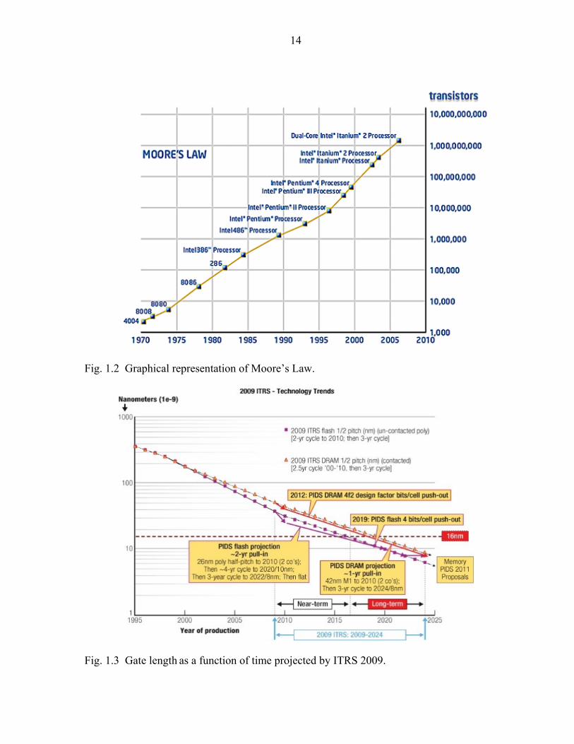
became essential to achieve better control.[5] With time, the dimensions of transistors be-
came smaller and smaller as described by Moore’s law which stated that the number density
of transistors would double every 18 months (Fig. 1.2). As such, with each technology node
the gate length (the distance between source and drain region) in transistors has also reduced.
The trend of decrease in gate length with time is shown in Fig. 1.3. This trend has also re-
sulted in a dramatic drop in the per unit cost of computing power for processors.[5] The oth-
er advantage of plasma processing of semiconductors is the capability of gaining better con-

4
trol in producing anisotropic profiles (vertical) as the combined effects of directional ions
and diffusive neutrals can create directional profiles, compared to round (isotropic) profiles
produced by wet etching, as shown in Fig 1.4. Also, choosing the appropriate plasma mix-
ture, the percentage composition of the mixture and bias allows one material to be etched,
with expected selectivity, relative to another.[15,16]
Another major application of plasmas is plasma-enhanced chemical vapor deposition
(PECVD).[17,18] In usual chemical vapor deposition (CVD), the deposition of a vapor on a
substrate may require activation energies (from the temperature of the substrate) that exceeds
the tolerances of the process. To increase the reactivity, the temperature of the substrate
must also be increased. However, when a plasma is used, some of the species in the gas
phase are excited which increase their reactivity with the heated substrate.[19] Consequent-
ly, a better growth rate of desired material can be achieved at a lower temperature than would
be possible without using plasmas. For interconnect technology, the CVD technique is ap-
plied for atomic layer deposition (ALD) of diffusion barrier metals such as Ti and Ta to pre-
vent the diffusion of Cu into the porous low-k material. Such low-k materials are used to re-
duce capacitance to enhance signal propagation speed. It has been reported that if plasma-
enhanced ALD is used, this kind of deposition process can be done at a much lower tempera-
ture, which is vital for the stability of low-k materials used in interconnect technology.[19-
22]
Selecting a plasma mixture to etch any material such as Si for semiconductor pro-
cessing, is primarily based on the volatility of the etch products. However, the selection can
be affected by other parameters, such as good directionality or good etch-profile control. For
example, etch rate for Si decreases in Cl-based plasmas compared to F-based plasmas and it
5
decreases even further if Br-based plasmas are used.[23] This is because deposition of Cl or
Br compounds on the surface passivates the surface preventing the Cl or Br radical to react
with Si. As such, the influence of energetic and directional ions has to increase to etch Si
where such protective Cl or Br layers first have to be ablated by energetic ions which will
expose Si, again, to etching agents of the plasma. Because of the enhanced influence of di-
rectional ions in the etching, Br-based plasmas will create a more vertical trench in Si as
compared to F or Cl-based plasmas.
Temperature control can also be a way to improve anisotropy or directionality of
etching.[23-26] Lowering temperature decreases the etching reaction probabilities between a
radical and the surface. Also, it increases the adsorption reaction probabilities. As such,
with a decrease in temperature there is a thicker formation of the passivation layer. In such a
process, surface area increases and ion induced reactions with the surface dominate neutral
reactions. Since the vertical etching component will dominate the lateral etching component,
a directional profile can be achieved by lowering the temperature. However, if the tempera-
ture is too low, the passivation layer will be too thick to allow the ions to interact with the
material.[23]
In plasma processing of semiconductors, the material to be processed is negatively
biased by the external power supply.[23] Thus, positive ions attracted by the negative bias
will bombard the wafer. Ions will cause both physical and chemical sputtering of the solid
which will enhance the etch rate. Radicals usually have >100 times higher flux than ions and
will play the dominant role in etching by chemically interacting with the surface and remov-
ing the molecules and atoms as volatile products. Radicals can also passivate the solid sur-
face with polymer like layers if the energy of the ions is not too high to sputter off the protec-
6
tive polymer coating. Formation of such protective layers, by radicals on a solid, will allow
etching of the solid selectively relative to another by controlling the energy of the ions in the
plasma so that the ion energy is higher than the etching threshold of the first solid, but lower
than the second. Major surface-plasma interaction mechanisms in plasma etching of a solid
are shown in Fig. 1.5.
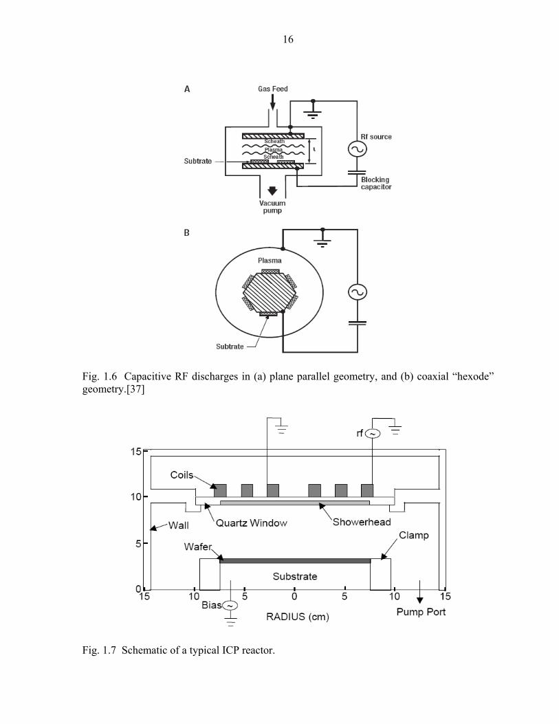
The two main types of reactors used for semiconductor etching are: capacitively cou-
pled plasma (CCP) system and inductively coupled plasma (ICP) system.[23] In a CCP sys-
tem (Fig. 1.6), bias is applied on the powered electrode so the energy of an ion is a function
of the power applied to feed the plasma. As such, ion fluxes and ion energies are not inde-
pendent parameters.[23] Generation of a high plasma density, which is essential for a high
flux of reactive species such as ions and photons, increases the energy of ions. Selective
etching of a solid, with a high density plasma, becomes impossible as ion energy increases
with the density of the plasma and such ions sputter off the protective passivation layer. On
the other hand, low pressure is necessary in plasma semiconductor processing to increase ion
bombardment efficiency. However, in a CCP, the electron-neutral collision mean-free path
can be of the same order of the gap between the CCP electrodes. As a result, sustaining the
plasma in a CCP becomes difficult.
The ICP system allows production of dense plasmas at low pressure without increas-
ing the ion energy.[27] Power is applied to the plasma by an inductive coupling between the
plasma and the antenna, through a dielectric window. No bias is applied between the plasma
and the chamber wall. The sample to be processed is located on a separate holder. The ener-
gy of ions in the plasma can be controlled independently from chamber pressure and plasma
density by biasing the substrate. As such, without increasing the ion energy, high plasma

7
density can be produced at a low pressure which enables formation of passivation layers on
sidewalls during trench etching (necessary for a vertical profile) and polymer deposition on a
solid to etch it selectively, relative to another solid. A schematic representation of a typical
ICP reactor is shown in Fig. 1.7.
1.3 Low-k Dielectric Integrity
Porous dielectrics, having a low dielectric constant (low-k), are being used to lower
the interconnect wiring capacitance in order to limit the RC time delay in integrated cir-
cuits.[28] SiCOH, silicon dioxide with CHx groups lining the pores, is one commonly used
material, having porosities as large as 50% with pore diameters of up to a few nm. The pores
can also be interconnected, offering pathways for reactive species to enter into the porous
network during plasma etching or cleaning steps.[28,29] Such penetrations are thought to
compromise the low-k nature of the material by removing the hydrophobic CHn groups that
surround the pore surface. Once a CHn group is removed, the Si atom attached to it adsorbs
moisture from ambient air which increases the RC time delay because the high k of water
(≈80) increases the overall dielectric constant of the low-k. As a result, a plasma treatment
that minimizes CHn group consumption is essential for maintaining porous low-k integrity.
In order to maintain the low-k values of porous dielectrics and to prevent penetration
of plasma species into the material, sealing of the pores at the surface may be necessary.[30]
Dielectrics are typically etched in fluorocarbon plasmas in which there is deposition of a CFx
polymer. The residual CFx polymer remaining at the end of the etch can, in fact, effectively
seal the pores.[31] While CFx polymers have good characteristics because of their low die-
lectric constant, the fluorine in the polymers might create compatibility issues with diffusion

8
barriers, including chemically active metals like Ti and Ta.[31] As such, the CFx polymer
must be removed while then implementing other more integration-compatible treatments for
pore sealing.
Due to its reactive nature, O2 plasmas were traditionally used for CFx polymer or PR
removal, however, less reactive H2/He plasmas can be more beneficial in protecting the sur-
face from damage while also activating the surface, so as to assist the subsequent sealing of
the porous surface. O2 plasmas contain O radicals which are very reactive and remove hy-
drophobic CHn groups efficiently with exothermic reactions. In He/H2 plasma cleaning, the
most reactive radical is H which removes both polymer and PR mildly because the etching
reactions are primarily endothermic. It has been reported that H2 plasmas cause insignificant
damage to the CHn groups. The other advantage in He/H2 cleaning is the less significant role
of the photons compared to O2 plasmas. O2 plasmas contain photons with wavelengths of
130 nm and beyond; such photons can penetrate >100 nm in the low-k causing Si-C bond
scission. Once a Si-C bond has been cleaved, adsorbed –CHn groups are easily etched by
reactive radicals. Thus, photons in O2 plasmas help O radicals to remove –CHn groups from
at least 100 nm deep sites. He/H2 plasmas include photons with wavelengths < 60 nm which
do not penetrate more than 20 nm in the low-k. As such, bond scission of Si-C bond in He/H2
plasma treatment is limited to 20 nm and H radicals can cause damage in the top 20 nm re-
gion of the low-k.
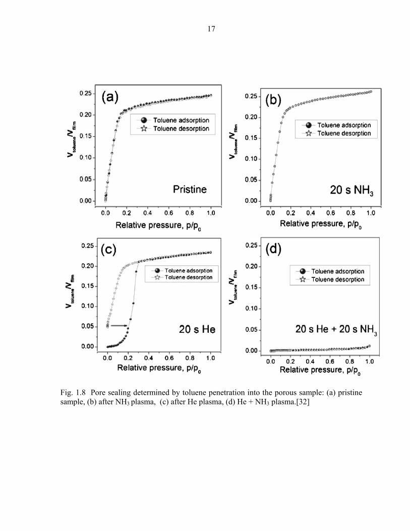
Sequential treatment of SiCOH by He and NH3 plasmas has been shown to seal pores
without surface damage while maintaining the low-k values of the SiCOH.[32] He plasmas
are thought to create active surface sites which localize and accelerate the chemical reactions
responsible for pore sealing.[32] It was found that if H2 is added to He, hot H atoms can im-

9
prove the surface activation as energetic H fluxes can remove H from surfaces and pore-
interior –CHn groups, thereby producing reactive –CHn-1 like groups. This is due to the fact
that hot H flux is not directional like the He+ which is the dominant agent for such activation
in He plasmas. Subsequent NH3 plasma treatment completes the sealing through formation
of Si-N, C-N and N-N bonds resulting from the chemisorption of NHx species.[32] The
bridging of these bonds across the opening of the pores effectively seals the pores. Such pore
sealing is able to prevent toluene penetration into the profile which validates the blocking of
surface pores (Fig. 1.8).[32]
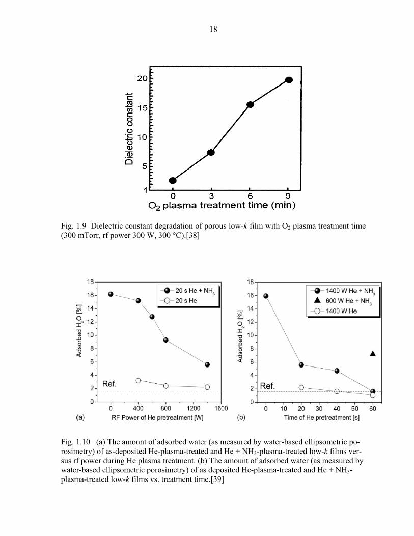
If the low-k is exposed to humidity after cleaning in Ar/O2 and He/H2 plasmas, ad-
sorption of H2O molecules by –CHn lost Si sites (–CHn were etched during cleaning) forms
Si-OH type products. Si-OH type compounds have a high-k which will increase the overall
dielectric constant of the porous material, with treatment time, as shown in Fig. 1.9. After
cleaning, if the low-k surface pores are sealed with NH3 plasmas, the sealing has been shown
to prevent water adsorption from humid air. This is because Si-N and C-N compounds
formed during sealing block water uptake pathways as shown in Fig. 1.10. As such, the seal-
ing layer is able to preserve the integrity of the low-k material.
A fully integrated multi-step etch, clean, activation and pore sealing processes using
Ar/O2 and He/H2 plasma cleans was modeled. The sequence begins with etching of an 8:1
aspect ratio trench in porous SiCOH using an Ar/C4F8/O2 CCP. Residual CFx polymers on
the sidewalls of the SiCOH were then removed using either Ar/O2 or H2/He inductively cou-
pled plasma (ICP). For Ar/O2 clean, subsequent surface activating He ICP followed by seal-
ing Ar/NH3 ICP treatments were applied to seal the pores open to the surface. For H2/He

10
plasma cleaning, surface sites were activated by hot H, He+ and photons present in the clean-
ing mixture, an Ar/NH3 treatment following the clean was sufficient for sealing.
After cleaning, the profile was exposed to humidity and included water in our model
resulting in the reactions between –CH3 free Si sites and H2O that form Si-OH type com-
pounds. The k degradation resulting from water uptake by the cleaned and unsealed profile
was numerically investigated. The degradation or rise in the k value after pore sealing was
also computationally investigated to see if sealing pores can preserve the low-k integrity by
blocking water uptake.
1.4 High-k Etching With Si Selectivity
As feature sizes decrease, the gate-silicon dioxide equivalent thickness required for
the insulator also decreases.[33] A larger oxide capacitance (thinner oxide layer) is neces-
sary to invert the surface to a sufficient sheet charge density in order to obtain the expected
transistor current for a given supply voltage. Continuing to reduce the insulator thickness
using SiO2 is problematic as leakage currents due to tunneling, increase as the thickness ap-
proaches a monolayer.[34] Consequently, high dielectric constant (high-k) metal oxides and
HfO2 in particular, are being implemented as replacements for SiO2 in gate-stacks to mini-
mize leakage currents resulting from thinning of the insulator. The larger dielectric constant
allows the oxide to be thicker for a given capacitance, thereby decreasing electric fields and
leakage currents. The gate length required for an SiO2 gate insulator as a function of time, as
projected by the 2009 International Technology Roadmap for Semiconductors (ITRS), is
shown in Fig. 1.3.
A high-k dielectric and a poly-Si gate are typically not suitable for high performance

11
for drive current.[34] Metal gates, having a higher free carrier density, maintain a high mo-
bility at junctions with high-k dielectrics and so many advanced designs incorporate metal
gates.[34] TiN is one such metal being considered for the gate.[35]
It has been found that HfO2 gate-stacks can be etched using BCl3/Cl2 plasmas, while
having a good selectivity to underlying Si by forming a BCln polymer on the Si which slows
its etching.[36] BnClm radicals coming from the plasma reacts with Si and forms a layer of
SixBy compounds. Formation of such SixBy layers is shown in Fig. 1.11. Once such a layer
is formed, BCln polymers are deposited and passivate the Si substrate. If the ion energy of
BCl3/Cl2 is controlled in such a way that it is higher than the etching threshold of HfO2 but
less than the Si etching threshold, an infinite selectivity for HfO2/Si etching can be achieved.
Fig. 1.12 shows the control of HfO2/Si selectivity by varying bias and BCl3 percentage in the
plasma.
A surface reaction mechanism for HfO2 etching in Ar/BCl3/Cl2 plasmas was devel-
oped and HfO2/Si selectivity was computationally investigated. In the model, Hf-O bond
breaking was the first step followed by Cl adsorption by Hf atoms that produced solid HfClx
and BClx adsorption by bond cleaved O that generated solid BmOCln. Later HfClx and
BmOCln solids were etched as volatile HfClx (x=2-4), BOCl, B2OCl3 and B2OCl4 by ion im-
pact reactions.
1.5 Summary
In Chapter 2, a detailed description of the Hybrid Plasma Equipment Model (HPEM),
which is the equipment scale model used in this work, is presented. The different modules of
the HPEM and the physics used for our simulations are explained. The Plasma Chemistry

12
Monte Carlo Model (PCMCM) in the HPEM generates the Energy and Angular Distributions
(EADs) of the different ions and neutral species on the wafer. Typical results from the
HPEM and PCMCM are presented.
In Chapter 3, the Monte Carlo Feature Profile Model (MCFPM) used for the simula-
tions in this work is explained in detail. The MCFPM uses the EADs from the PCMCM as
input. Typical results for integrated modeling of semiconductor processes (etch, clean and
pore sealing) are presented.
In Chapter 4, the pore sealing mechanisms of porous low-k SiCOH with successive
He and NH3 plasmas are described. Effects of some parameters, such as pore radius, aspect
ratio of the trench and plasma treatment time have been described in detail.
In Chapter 5, plasma damage during CFx polymer cleaning and PR stripping in Ar/O2
and He/H2 plasmas have been summarized and compared. The impact of photons on the
damage mechanism has been explained. The degree of plasma damage in the low-k material
is estimated by the damage depth or the depth of a SiO2-CH3 site that has lost the −CH3
group due to its interaction with plasma species.
In Chapter 6, low-k degradation mechanisms or the mechanisms responsible for the
increase in dielectric constant of porous SiCOH film have been described. The degradation is
compared between Ar/O2 and He/H2 plasma cleaning. Preservation of low-k Integrity by pore
sealing, after cleaning to block water uptake, has been numerically investigated.
In Chapter 7, reaction mechanisms for a TiN/HfO2/SiO2/Si gate stack etching in
Ar/BCl3/Cl2 plasmas and PR trimming in Ar/O2 plasmas have been described. Achievement
of a high HfO2/Si selectivity in the plasma was investigated by varying substrate bias.

13
1.6 Figures
Fig. 1.1 Plasma processes arranged by operating pressure. As the pressure increases, the character of the process tends to move from physical to chemical to thermal in nature.[2]
14
Fig. 1.2 Graphical representation of Moore’s Law.
Fig. 1.3 Gate length as a function of time projected by ITRS 2009.

15
Fig. 1.4 Plasma etching in integrated circuit manufacturing: (a) an example of an isotropic etch; (b) a sidewall etching of the resist mask which leads to a loss of anisotropy in film etch; (c) illustrates the role of bombarding ions in an isotropic etch; (d) illustrates the role of side-wall passivating films in an isotropic etch.[37]
Fig. 1.5 Four basic plasma etching processes: (a) sputtering; (b) pure chemical etching; (c) ion energy-driven etching; (d) ion-enhanced inhibitor etching.[37]
16
Fig. 1.6 Capacitive RF discharges in (a) plane parallel geometry, and (b) coaxial “hexode” geometry.[37]
Fig. 1.7 Schematic of a typical ICP reactor.
17
Fig. 1.8 Pore sealing determined by toluene penetration into the porous sample: (a) pristine sample, (b) after NH3 plasma, (c) after He plasma, (d) He + NH3 plasma.[32]
18
Fig. 1.9 Dielectric constant degradation of porous low-k film with O2 plasma treatment time (300 mTorr, rf power 300 W, 300 °C).[38]
Fig. 1.10 (a) The amount of adsorbed water (as measured by water-based ellipsometric po-rosimetry) of as-deposited He-plasma-treated and He + NH3-plasma-treated low-k films ver-sus rf power during He plasma treatment. (b) The amount of adsorbed water (as measured by water-based ellipsometric porosimetry) of as deposited He-plasma-treated and He + NH3-plasma-treated low-k films vs. treatment time.[39]

19
Fig. 1.11 Protective BxCly layer formation which is essential for a good HfO2/Si selectivi-
ty.[40]
Fig. 1.12 Etch and deposition rates on HfO2, SiO2 and p–Si as a function of (a) bias power in pure BCl3 plasma/clean walls, and (b) argon dilution at 10W bias/clean walls. The colored zones represent conditions for which infinite selectivity is achieved.[40]

20
1.7 References
1. L. E. Kline and M. J. Kushner, Crit. Reviews in Solid State and Materials Sci. 16(1), 1
(1989).
2. J. L. Shohet, IEEE Trans. Plasma Sci., Vol. 19( 5), 725 (1991).
3. Special Issue on Thermal Plasma Processing, Plasma Chem. Plasma Process., vol. 9
(suppl.), 1989.
4. D. M. Manos and D. L. Flamm, in Plasma Etching, D. M. Manos, Ed. San Diego: Har-
court, Brace, Jovanovich, 1989.
5. D. B. Graves, IEEE Trans. Plasma Sci., Vol. 22( 1), 31 (1994).
6. D. B. Graves, AIChE J. 35, 1 (1989).
7. S. M. Rossnagel, J. J. Cuomo, and W. D. Westwood, Eds., Handbook of Plasma Pro-
cessing Technology. Park Ridge, NJ: Noyes Publications, 1990.
8. J. W. Cobum, Plasma Etching and Reactive Ion Etching, New York: AVS Monograph
Series, 1982.
9. B. Chapman, Glow Discharge Processes, New York, Wiley, 1980.
10. T. Sugano, Applications of Plasma Processes to VLSl Technology, New York: Wiley,
1985.
11. N. G. Einspruch and D. M. Brown, Eds., VLSI Electronics Microstructure Science,
Plasma Processing for VLSI, Orlando: Academic, vol. 8, 1984.
12. D. Manos and D. Flamm, Plasma Etching, San Diego: Academic, 1988.
13. M. Konuma, Film Deposition by Plasma Techniques, Berlin: Springer-Verlag, 1992.
14. P. K. Chu, S. Qin, And C. Chan, N. W. Cheung, And P. K. Ko, IEEE Trans. on Plasma
Sci. 26( 1), 79 (1998).

21
15. H. Abe, Y. Sonobe, and T. Enomoto, Jpn. J. Appl. Phys. 12, 287 (1973).
16. F.H. Bell, O. Joubert, G.S. Oehrlein, Y. Zhang, D. Vender, J. Vac. Sci. Technol. A 12,
3095 (1994).
17. Handbook of Plasma Processing Technology: Fundamentals, Etching, Deposition, and
Surface Interactions, edited by S. M. Rossnagel, J. J. Cuomo, and W. D. Westwood
(Noyes, Park Ridge, NJ, 1990).
18. R. Reif and W. Kern, in Thin Film Process II, edited by J. L. Vossen and W. Kern (Aca-
demic, New York, 1991).
19. S. M. Rossnagel, A. Sherman, and F. Turner, J. Vac. Sci. Technol. B 18(4), 2016 (2000).
20. H. Kim, J. Vac. Sci. Technol. B 21(6), 2231 (2003).
21. H. Kim, A. J. Kellock, and S. M. Rossnagel, J. Appl. Phys. 92, 7080 (2002).
22. J.-S. Park, M. J. Lee, C.-S. Lee, and S.-W. Kang, Electrochem. Solid-State Lett. 4, C17
(2001).
23. Christophe Cardinaud, Marie-Claude Peignon, and Pierre-Yves Tessier, Appl. Sur.
Sci. 164, 72 (2000).
24. S. Tachi, K. Tsujimoto, S. Arai, T. Kure, J. Vac. Sci. Technol. A 9, 796 (1991).
25. T. Chevolleau, P.-Y. Tessier, Ch. Cardinaud, G. Turban, J. Vac. Sci. Technol. A 15,
2661 (1997).
26. P.-Y. Tessier, T. Chevolleau, Ch. Cardinaud, B. Grolleau, Nucl. Instrum. Methods B
155, 280 (1999).
27. W.L. Johnson, in: O. Popov (Ed.), High Density Plasma Sources, Noyes Data Corp.,
Park Ridge, NJ, 1979.

22
28. C. M. Whelan, Q. T. Le, F. Cecchet, A. Satta, J. J. Pireaux, P. Rudlof, and K. Maex,
Electrochem. Solid-State Lett. 7, F8 (2004). [28]
29. G. Beyer, A. Satta, J. Schuhmacher, K. Maex, W. Besling,O. Kilpela, H. Sprey, G.
Tempel, Microelectron. Eng. 64, 233 (2002).
30. T. Abell and K. Maex, Microelectron. Eng. 76, 16 (2004).
31. G. Mannaert, M. R. Baklanov, Q. T. Le, Y. Travaly, W. Boullart, S. Vanhaelemeersch,
and A. M. Jonas J. Vac. Sci. Technol. B 23, 2198 (2005).
32. M. Urbanowicz, M. R. Baklanov, J. Heijlen, Y. Travaly, and A. Cockburn, Electrochem.
Solid-State Lett. 10, G76 (2007).
33. B. H. Lee, L. Kang, R. Nieh, W.-J. Qi, and J. C. Lee, Appl. Phys. Lett. 76, 1926 (2000).
34. R. Chau, J. Brask, S. Datta, G. Dewey, M. Doczy, B. Doyle, J. Kavalieros, B. Jin, M.
Metz, A. Majumdar, and M. Radosavljevic, Microelectron. Engr. 80, 1 (2005).
35. R. Chau, S. Datta, M. Doczy, B. Doyle, J. Kavalieros, and M. Metz, Elect. Dev. Lett. 25,
408 (2004).
36. O. Joubert , E. Sungauer, E. Pargon, X. Mellhaoui, R. Ramos, G. Cunge and L. Valier ,
J. Vac. Sci. Technol. B 25, 1640 (2007).
37. Pall corporation research, http://www.pall.com/pdfs/Microelectronics/ABG-106-
0405.pdf.
38. K. Maex, M. Baklanov, D. Shamiryan, F. Iacopi, S. H. Brongersma, K. Maex, and Z. S.
Ya novitskaya, J. Appl. Phys. 93, 8793 (2003).
39. A. M. Urbanowicz, D. Shamiryan, A. Zaka, P. Verdonck, S. De Gendt and M. R. Bak-
lanov, J. Electrochem. Soc. 157, H565 (2010).

23
40. E. Sungauer, X. Mellhaoui, E. Pargon, and O. Joubert, Microelectron. Eng. 86, 965
(2009).

24
2. HYBRID PLASMA EQUIPMENT MODEL
2.1 Introduction
The Hybrid Plasma Equipment Model (HPEM) was developed for simulating low-
temperature, low-pressure plasma processes such as plasma etching and plasma-assisted dep-
osition.[1-18] The HPEM has been used to predict the reactor scale plasma characteristics
and reactant fluxes to surfaces in the ICP reactor.
The HPEM is a two-dimensional (2D), modular model which addresses gas phase and
surface kinetics. (See Fig. 2.1) The HPEM addresses plasma physics and plasma chemistry
in a modular fashion. There are three main blocks: The Electromagnetic Module (EMM), the
Electron Energy Transport Module (EETM) and the Fluid Kinetic Module (FKM). Electro-
magnetic fields are derived by solving the frequency domain wave equation based on coil
currents adjusted to deliver a specified power deposition. The spatially dependent power
deposition is used as a source term in obtaining the electron temperature, Te, from an electron
energy conservation equation. Transport and rate coefficients as function of average electron
energy are obtained from a solution of Boltzmann’s equation, and a Monte Carlo simulation
is used to follow the trajectories of sheath accelerated secondary electrons. The transport co-
efficients and source functions are used by the FKM to solve separate continuity, momentum,
and energy equations for each ion and neutral species, while semi-implicitly solving Pois-
son’s equation for the time varying electrostatic potential. The densities and electrostatic
fields from the FKM are then transferred to the other modules. This process is iterated until a
converged quasi-steady state solution is obtained.
Several off-line modules of the HPEM have been developed for other specific pur-
poses. The Plasma Chemistry Monte Carlo Simulation (PCMCS) computes energy and angu-

25
lar dependencies of fluxes at specified surface locations by using outputs from the HPEM
[6]. The Monte Carlo Feature Profile Model (MCFPM) uses the results of the PCMCS or the
PCMCM to simulate nanoscale feature profile evolution [15]. The physics of these modules
contained in the HPEM will be described in the following sections. Also, typical results from
the HPEM will be presented.
The Monte Carlo Radiation Transport Module (MCRTM) inputs the gas densities,
temperatures, pressures, collision frequencies and rate coefficients for all the gas phase reac-
tions (including radiative reactions), and modifies the rate coefficient for the radiative reac-
tions. The Surface Chemistry Module (SCM) reads in fluxes to the surfaces of interest and
returns sticking coefficients and modified gas fluxes from the surface, after the surface reac-
tions are computed. Both MCRTM and SCM will be described in the upcoming chapters.
2.2 The Electromagnetic Module
Starting with an initial guess of plasma properties, the EMM computes the inductive-
ly coupled electric fields determined by the inductive coils and the magnetostatic fields in-
duced by permanent magnets or dc current loops. These fields are passed to the EETM. The
EMM computes time varying electric and magnetic fields for the HPEM.
The EMM module calculates the spatially dependent azimuthal electric fields by solv-
ing Maxwell’s equation under time harmonic conditions. Assuming azimuthal symmetry,
Maxwell’s equation for electric fields is reduced to
φφφ ωεωµ
JiEE −=∇⋅∇ 21 , (2.1)

26
where µ is the permeability, Eφ is the azimuthal electric field, ω is the frequency of the
source current, ε is the permittivity, and Jφ is the total current consisting of driving and con-
duction currents. The conduction current Jc is calculated from Jc =σ Eφ, where σ is the con-
ductivity. For collisional plasmas, the plasma conductivity is
ω
σivm
nqmee
ee
+=
12
, (2.2)
where qe is the unit electron charge, ne represents electron density, me denotes electron mass,
vme is the momentum transfer collision frequency of electrons, and ω is the driving frequency.
Maxwell’s equations are solved using the successive over-relaxation (SOR) technique. The
weighting coefficient and the convergence criterion for the SOR are adjustable simulation
parameters.
The static magnetic fields are solved in the radial and axial directions assuming azi-
muthal symmetry. DC current loops are used for this calculation. For a mesh that contains a
permanent magnet, the code replaces the corresponding grid points with small current loops.
The magnetic field can be computed through a vector A, which satisfies
BA =×∇ ; jA =×∇×∇µ1 ; (2.3)
where µ is the permeability, and j is the current density of the source current loops.
2.3 The Fluid Kinetics Module
Fluid equations are solved in FKM to obtain plasma species densities and fluxes. The
FKM also computes electrostatic fields by either solving Poisson’s equation or using an am-
bipolar field approximation. Transport coefficients and source functions are used by the

27
FKM to solve separate continuity, momentum, and energy equations for each ion and neutral
species, while semi-implicitly solving Poisson’s equation for the time varying electrostatic
potential.
The continuity equation that describes the density evolution rate for any species is
iii S
tN
+Γ⋅−∇=∂
∂ , (2.4)
where Ni is the density, Γi denotes the flux, and Si represents the source term determined by
plasma chemical reactions. Rate coefficients for electron impact reactions are obtained from
the EETM, and heavy particle reaction coefficients are supplied to the code. These values are
used to calculate the source terms. For both electrons and heavy particles, the fluxes can be
calculated from the drift-diffusion equation:
kkkkkk E NDNq ∇−=Γ µ , (2.5)
where µ is the mobility, q is the charge, N is the density, and D is the diffusion coefficient.
The transport properties of electrons are obtained from the EETM results. For ions and neu-
trals, the transport properties are either taken from a database or calculated from Lenard-
Jones parameters.
Ion and neutral fluxes can also be solved from the momentum equation:
( ) ( ) ( ) ( ) ijjij
jiji
jii
i
ijiiii
i
i vNNmm
mN
mqNkTN
mtvvBvEvv −
+−⋅∇−×++⋅∇−∇−=
∂Γ∂ ∑τ1 , (2.6)
where Γi, mi, k, Ni, Ti, and vi denotes the flux, mass, Boltzmann constant, density, tempera-
ture, and velocity, respectively, of the species i; mj and Nj are the mass and density, respec-
tively, of the species j; νij is the collision frequency between species i and j. Here τ is the vis-
cosity tensor for neutral species, and it is only used in the neutral momentum equation.

28
Determination of the time-dependent electrostatic fields is accomplished either by
solution of Poisson’s equation or based on quasi-neutrality allowing an ambipolar approxi-
mation. These are two alternative ways for the FKM to calculate the electrostatic fields. In
the first method the time-evolving electrostatic potential φ is related to the net charge density
as
ρφε −=⋅ ∇∇ , (2.7)
where ε is the permittivity, φ is the electrostatic potential, and ρ is the net charge density. To
enable an implicit solution, the charge density at the time when φ is required is numerically
estimated using a first-order Taylor series expansion:
tt
ttt
tt
∆+∆+ ⋅∆+=
∂∂ρρρ , (2.8)
where tt ∆+ρ is the charge density at time t+∆t, and tρ is the charge density at time t. The evo-
lution rate of the charge density ∂ρ/∂t is determined by the gradient of the total current densi-
ty j:
St
+⋅−∇=∂∂ jρ , (2.9)
where S is the source function of charges. In the plasma region,
∑ −∇+∇−=i
iiiii qnDq ))(( φµj ; in materials, ( )φσ ∇−=j where σ is the material conductivi-
ty.
The second option to compute electrostatic fields in the FKM is to use a quasi-
neutrality approximation over the entire plasma region. Under such an assumption, the elec-
29
tron density is equal to the total ion charge density at all locations. This requires that when
using drift-diffusion equations for both electrons and ions, at steady state,
( )∑ +Γ⋅∇=+Γ⋅∇i
iiiee SqS , (2.10)
or
∑ +∇+∇−⋅∇=+∇+∇⋅∇i
iiiiiieeeee SnDnqSnDn ))(()( φµφµ . (2.11)
In the above equations, Se and Si represent electron and ion source functions, respectively, and
the right-hand side of the equations sum over all charged species. From Eq. 2.11, the electro-
static potential can be determined from species densities and species source functions.
2.4 The Electron Energy Transport Module
The EETM calculates electron kinetics properties such as the electron energy distri-
bution function, electron temperature, and electron impact rate coefficients. There are two
ways for the EETM to calculate the electron energy distribution function. The first method is
to solve the 2-D electron energy equation. Electron transport properties are obtained by solv-
ing the 0-D Boltzmann equation. The second approach of the EETM is to use an electron
Monte Carlo simulation (EMCS). The EEDF is then obtained from the collected statistics.
Under the influence of electric fields, free electrons are accelerated to high energies,
on the order of several electron volts. These electrons then inelastically collide with neutrals,
leading to neutral dissociation, excitation, and ionization. The electron impact reaction rates
strongly depend on the electron temperature Te, which is related to the electron energy distri-
bution function (EEDF) as
∫ )(5.1 εεε dfTe ⋅⋅= , (2.12)

30
where ε represents electron energy and f(ε) is the electron energy distribution function. Ine-
lastic collisions influence the EEDF by extracting energy from electrons, resulting in a reduc-
tion of the high-energy tail of the EEDF. As a result, for collisional plasmas, the EEDF does
not behave as a Maxwellian distribution. The EETM was designed to simulate this effect.
2.4.1 The Electron Energy Equation Method
The 0-Boltzmann equation is expressed as
collision
ee
ee
e
tff
mef
tf
⎟⎠⎞
⎜⎝⎛
∂∂
=∇×+
−∇⋅+∂∂
vrBvEv )( , (2.13)
where fe = fe(t, r, v) is the electron distribution function, ∇r is the spatial gradient, ∇v is the
represents velocity gradient, me is the electron mass, and collision
e
tf
⎟⎠⎞
⎜⎝⎛
∂∂ represents the effect of
collisions. The EEEM solves the 0-dimensional Boltzmann equation for a range of E/N (elec-
tric field divided by total gas density). The electron temperature and all of its dependent
quantities, like electron impact rate coefficients and electron mobility, are derived from the
EEDF.
Results of the 0-dimensional Boltzmann equation are then used to solve the electron
energy equation:
lossheatingeee PPTT −=Γ⋅∇+∇∇ )(κ , (2.14)
where k is the thermal conductivity, Te is the electron temperature, Γe is the electron flux,
Pheating is the electron heating due to deposition, and Ploss is the power loss due to inelastic
collisions. Pheating is computed from the time averaged value of j⋅E, where j is the electron
current obtained from the FKM, and E is the electric field due to both inductively and capaci-

31
tively coupled effects. The electric field is both the inductive field computed in the EMM and
the capacitively coupled field computed in the FKM.
2.4.2 The Electron Monte Carlo Simulation
The Monte Carlo method is a fully kinetic treatment, which resolves the acceleration
of electrons in electric fields and the gyro motion of electrons in magnetic fields using a
semi-implicit technique. Non-collisional heating is kinetically resolved by producing electron
currents, which are used to correct the assumption of collisional power deposition in the
EMM.
The EMCS tracks the trajectories of electron pseudoparticles in the electromagnetic
fields obtained from the EMM module and the electrostatic fields obtained from the FKM.
Statistics on electron energy distributions are gathered by tracking the particle motion and
collisions. The electrons are initially given a Maxwellian distribution and are spatially dis-
tributed according to the electron density distribution calculated by the FKM. Electrons are
accelerated by the electromagnetic and electrostatic fields in a manner governed by the Lo-
rentz equation:
( )BvEv×+=
e
e
mq
dtd , (2.15)
where v is the velocity (dr/dt = v where r is the location). Collisions can also alter electron
energy and location. Energy-dependent collision cross sections and energy losses due to col-
lisions are supplied to the EMCS. EMCS also generates spatially dependent electron temper-
ature, electron impact rate coefficients, and collision frequencies.

32
2.5 The Plasma Chemistry Monte Carlo Module
The PCMCM produces the energy and angular distributions for neutrals and ions
striking surfaces in contact with the plasma. The PCMCM launches pseudoparticles repre-
senting ions and neutrals based on the electron impact source functions. Using time depend-
ent electric fields from the FKM, their trajectories are integrated while accounting for gas
phase collisions. The energy and angular distributions (EADs) of ion (IEADs) and neutral
pseudoparticles are recorded as they strike surfaces.
PCMCM module was originally a postprocessor to the HPEM that was later incorpo-
rated into the HPEM. It used volumetric sources of plasma species, time-dependent electric
fields, and sheath properties exported from the HPEM to obtain the angular and energy dis-
tributions of the fluxes using Monte Carlo techniques.[6] The PCMCM functions in a similar
manner but also accounts for nonthermal, or in-flight fluxes, resulting from sputter sources in
addition to the volumetric sources. Sputtered atoms and neutralized ions which are reflected
from the target have kinetic energies of several eV. These species are not initially in thermal
equilibrium with the buffer gas, which has a temperature of ≤0.3 eV. Under certain process
conditions, these energetic particles may not thermalize prior to reaching the wafer. The tra-
jectories and energies of these nonequilibrium particles are already tracked by the sputter al-
gorithms in the FKM. Statistics on the energy and angular distributions of the particles as
they strike selected surfaces are collected and passed to the PCMCM.
Based on these quantities, a rate of generation of species i as a function of position,
( )rGRir (cm-3 s-1), is computed. This generation term accounts for all sources of species i on
the right- and side of reactions in the mechanism. The rate ( )rGRir also includes source func-
tions on surface s due to, for example, sputtering. In a similar fashion, a consumption rate

33
( )rCMir (cm-3 s-1) is computed based on all reactions containing species i on the left-hand
side of reactions in the mechanism. A local elastic collision frequency with each species is
also computed. These elastic frequencies are added to the local consumption frequency
( ) ( )rVrCMirr ∆ where ( )rV r
∆ is the volume of the computational cell at location rr to yield a
total interaction frequency ( )rvTr . Null collision techniques are used at each spatial location
to provide a reactor wide collision frequency vi for each species i, which simplifies the ran-
dom selection of collision times and mean free paths for individual particles.
The Null collision algorithm was proposed by Skullerud.[19-21] For a particle i, drift-
ing through a gas of density N under the influence of an electric field where the collision fre-
quency is velocity dependent, the development of the algorithm was driven by the necessity
for a simple and fast method to determine the free time ∆t between two successive collisions.
If the collision frequency vi is constant, the mean-free time between collisions TMFT is also
constant, and ∆t can be obtained from the following relationship:
)ln(1 rv
ti
−=∆ (2.16)
where r is a rectangularly distributed random number on the interval 0 < r < 1.
According to Skullerud’s null algorithm, a particle at any point in a simulation with
an arbitrary energy E can be assigned a constant trial collision frequency vi’ which is greater
than the real collision frequency vi.[19-21] Simulation of the motion of a particle up to the
time of the next collision(associated with vi’ ) can be described as follows. A random number
is chosen to determine a free time ∆t (evaluated from relationship (2.8) and noting that TMFT
= l/vi’ ) during which the simulated particle is accelerated by the external field. At the end of
the interval ∆t, another random number P is chosen. I f P is greater than vi/vi’, evaluated at

34
the energy immediately prior to collision, the particle is considered to have suffered a null
collision. If a null collision happens, the particle is undeflected and the program returns to
choose the next ∆t. A real collision involves appropriate calculations for scattering of the
particle from the target gas before a subsequent ∆t is chosen. After each collision, null or
real, a new vi’ may be chosen. Many such free paths are simulated to obtain statistically sig-
nificant results, during which time the phase-space coordinates of the particle are sampled in
some fashion to determine the transport parameters. It is well established that the above
method is faster than performing the integrations required to explicitly determine the free
time between collisions for a real cross section.[21]
In the PCMCM, pseudoparticles of species i are launched from each computational
cell at a time randomly chosen in the rf cycle with a weighting (or total number) proportional
to ( ) ( )rVrGRirr ∆ . The velocity is randomly chosen from a Maxwell-Boltzmann distribution
having a local temperature ( )rTir for volumetric sources where the spatially dependent tem-
perature for each species is computed by HPEM. The trajectories of the pseudoparticles are
integrated for the time ∆t for a random number r (0 <r <1) using equation 2.16.
At the end of the time step, Monte Carlo techniques are used to determine if the colli-
sion is real or null. If real, another random number is used to determine if the collision is
elastic or consuming. If consuming, the particle is removed from the simulation. If elastic,
the collision partner is identified using another random number and the velocity of the pseu-
doparticle is changed appropriately using standard elastic collision techniques. The one ex-
ception is for charge exchange collisions which are separately accounted for in the sum of
collision frequencies. If an ion undergoes a charge exchange collision, its identity is changed
to the neutral counterpart and the trajectory is retained. The trajectories are advanced until
35
the pseudoparticles reach the vicinity of a surface. If the surface is chosen as one for which
statistics on incident species are desired, ions are then integrated through the sheath, a com-
putationally expensive process. For surfaces not selected, the particles are removed from the
simulation. A similar process is followed for the neutrals, except for integration through the
sheath.
2.6. Monte Carlo Radiation Transport Model
The MCRTM in the HPEM is called after each iteration to provide photon fluxes in-
cident onto the SiOCH.[22] The operation of MCRTM is similar to the operation of
PCMCM. Source functions for launching of pseudoparticles representing photons are de-
rived from the excited state densities generated by the FKM. The trajectory of a photon is
tracked until it is absorbed by a gas phase species or it strikes a surface. The photon absorp-
tion probability is obtained from a Voight line-shape function using the natural lifetime, col-
lisional broadening and Doppler broadening produced by the local gas densities and tempera-
tures. If resonantly absorbed, photons are re-emitted using a partial-frequency redistribution
algorithm. The fluxes and spectra of photons are recorded as a function of the material the
photons strike, and are exported to the surface kinetics module SCM of the HPEM. The rates
of photon absorption and re-emission are recorded for each optical transition, and are used to
calculate radiation trapping factors which lengthen the natural lifetime of the emitting spe-
cies. These factors are exported to the FKM.
The MCRTM has been described in detail in an earlier literature.[22] The MCRTM
tracks quanta of energy emitted by plasma excited species as the photon is absorbed and re-
emitted while traversing the plasma. As the probability for absorption and re-emission de-

36
pends on local densities of the absorbing and emitting species, the densities of quenching and
lineshape perturbing species and the gas temperature, the MCRTM was interfaced to the
HPEM, which provides these quantities. In turn, the MCRTM provides the effective lifetime
of emitting excited states for use in the plasma kinetics routines of the HPEM.
The MCRTM directly interfaces with the FKM on each iteration through the HPEM.
The parameters provided by the FKM to the MCRTM are species densities, gas temperatures
and rate constants, from which the frequencies for perturbing and quenching collisions af-
fecting the species participating in radiative transfer reactions are calculated. The MCRTM
produces radiation trapping factors which are used to modify the lifetime of radiating species
during the next execution of the FKM. The algorithms used in the MCRTM are similar to
those described by Sommerer.[23] Pseudoparticles representing photons are tracked from
their site of emission through multiple absorptions and re-emissions until their escape from
the plasma or until the quanta of energy is quenched. Although reflection from surfaces can
be accounted for, we assumed that all surfaces are absorbing or transmitting and so any pho-
ton which strikes a surface is lost from the plasma.
Pseudoparticles are emitted from sites randomly distributed within a numerical mesh
cell in proportion to the density of radiators in that cell (obtained from the FKM). As the
densities of radiators may vary by orders of magnitude over the plasma region, the number of
pseudoparticles released from each cell i is rescaled to ensure that a statistically relevant
number of pseudoparticles is emitted from every cell.
( ) ⎟⎟⎠
⎞⎜⎜⎝
⎛−
−−+= *
min*max
*min
*
minmaxmin loglogloglog
NNNNnnnn i
i (2.17)
where ni is the number of pseudoparticles emitted from cell i, and nmin and nmax are preselect-

37
ed minimum and maximum number of pseudoparticles permitted to be emitted and is the
density of the radiating species in cell i. *minN and *
maxN are the minimum and maximum den-
sities of N* in the plasma. These values are dynamically determined during execution of the
model. A weighting wi is assigned to each pseudoparticle for the purposes of collecting sta-
tistics. For a pseudoparticle emitted from cell i,
∏ ,=m
imi ww (2.18)
where wm is a series of subweightings. The first such subweighting is
i
iii n
VNw
∆=,1 (2.19)
where ∆Vi is the volume of cell i.
The frequency of the photon is then selected from the lineshape function g(ν), the
probability of a photon being emitted at a frequency.[24] The likelihood of the photon being
emitted near line center can be hundreds to thousands of times higher than being emitted in
the far wings of the lineshape. The majority of photons escaping the plasma usually originate
from the wings of the lineshape, where absorption probabilities are smaller. Selecting pseu-
doparticles with probabilities directly proportional to g(ν) would, in the absence of using a
very large number of pseudoparticles, undersample the wings of the lineshape. Although the
assignment of frequency directly proportional to g(ν) is the least ambiguous method, the need
to avoid sampling problems in 2-dimensions and the desire to obtain frequency resolution
throughout the mesh motivates one to try another method. To avoid the statistical under-
sampling in the wings of the lineshape profile, we instead uniformly distribute the pseudopar-

38
ticles over a preselected range of frequencies about the line center ν0, and use an additional
weighting factor ( )vgw =2 to account for the likelihood of emission.
2.7 Surface Chemistry Model
The capability to address surface reactions in the HPEM was achieved with the crea-
tion of the SCM.[25] The SCM addresses surface reactions in the HPEM using a flux in –
flux out boundary condition. The physics of this model has already been described in an ear-
lier literature.[25] The SCM implements a modified surface-site balance algorithm along the
plasma-surface boundary, and outputs surface coverages, thickness and composition of over-
laying films, reactive sticking coefficients, and modified fluxes of species returning to the
plasma. Aside from the gaseous species being directly available as surface reactants, there is
also the possibility (e.g. in fluorocarbon plasmas), of overlaying films, through which the
gaseous species diffuse to the available surface sites. In addition, the constituents of the film
may also react with the gaseous species and the underlying substrate. The SCM is capable of
handling all of the above processes.
Reaction probabilities for gas phase species with surfaces are provided by the SCM
which computes the composition of surface resident species using a multilayer surface-site-
balance model. The reaction mechanism is unique for each surface in contact with the plas-
ma. The PCMCM produces the energy and angular distributions for neutrals and ions strik-
ing surfaces in contact with the plasma. The PCMCM launches pseudoparticles representing
ions and neutrals based on the electron impact source functions. Using time dependent elec-
tric fields from the FKM, their trajectories are integrated while accounting for gas phase col-
lisions. The energy and angular distributions (EADs) of ion (IEADs) and neutral pseudopar-

39
ticles are recorded as they strike surfaces.
The SCM incorporates energy dependent reaction probabilities based on the EADs
obtained from the PCMCM. The probabilities for surface reactions involving energetic spe-
cies (either ions or hot neutrals) are given by [23]
p(E) = p0 mt
mr
mt
m
EEEE
−− (2.20)
where p(E) is the reaction probability for a particle with energy E, Et is the threshold energy
of the process, Er is a reference energy, and po is the reaction probability at the reference en-
ergy. We used m = 0.5 for sputtering or ion activated etching.
2.8 Typical Results from the HPEM
The results of HPEM simulations include 2-D distributions of fields, species densi-
ties, species fluxes, power deposition and source functions. HPEM outputs for an example
case are discussed in this section for an ICP discharge sustained in He/H2 gas mixture.The
schematic of the cylindrical reactor used in this simulation is shown in Fig. 2.2a.
The reactor is 13 cm in radius and 17 cm in height. The inductive power is supplied
through a three-turn antenna coil above a 0.8 cm thick quartz window. The wafer is on an
independently powered substrate 9 cm below the quartz window. The wafer, 15 cm in diam-
eter and 9 cm below the top inside wall, sits on an rf-biased substrate. He/H2 is supplied
through the gas nozzle at a flow rate of 100 sccm. The pressure is stabilized at 10 mTorr.
ICP reactor was sustained in a 10 mTorr He/H2 = 75/25 mixture and was powered at 13.56
MHz with a 10 MHz bias on the substrate. The H2 and H2+ ion densities in the reactor are

40
shown in Fig. 2.2b and Fig. 2.2c, respectively. The total ion density has a maximum of 5 ×
1010 cm-3 while the H atom density has a maximum of 2 × 1013 cm-3, depleted in the center of
the reactor due to gas heating (up to 800 K). The IEADs for major ions and the combination
of ions is shown in Fig. 2.3. Major fluxes to the wafer are shown in Fig. 2.4a as a function of
the reactor radius. The energy and angular distributions of H is shown in Fig. 2.4b. The ion
fluxes (≈1016 cm-2s-1) largely responsible for the PR removal in semiconductor processing,
have an average energy near 25 eV and an angular spread from the vertical of <350. The H
atom fluxes have a nearly isotropic angular distribution and a peak at a maximum at < 1000
K. However, the tail of the energy distribution extends to above 10 eV.

41
2.9 Figures
Fig. 2.1 Schematic representation of the HPEM modular model.

42
Fig. 2.2 (a) Schematic of the ICP reactor. (b) H2 density inside the reactor. (c) H2
+ density distribution inside the reactor.

43
Fig. 2.3 Energy and angular distributions of ions in the He/H2 plasma: (a) H+; (b) H2
+; (c) all ions combined.
Fig. 2.4 Major fluxes in the He/H2 plasma and neutral H energy and angular distributions: (a) major radical and ion fluxes; (b) 2-D H energy and angular distribution.

44
2.10 References 1. T. J. Sommerer and M. J. Kushner, J. Appl. Phys. 71, 1654 (1992).
2. P. L. G. Ventzek, R. J. Hoekstra, T. J. Sommerer, and M. J. Kushner, Appl. Phys. Lett.
63, 605 (1993).
3. P. L. G. Ventzek, R. J. Hoekstra, and M. J. Kushner, J. Vac. Sci. Technol. B 12, 461
(1994).
4. P. L. G. Ventzek, M. J. Grapperhaus, and M. J. Kushner, J. Vac. Sci. Technol. B 12,
3118 (1994).
5. F. Y. Huang and M. J. Kushner, J. Appl. Phys. 78, 5909 (1995).
6. R. J. Hoekstra and M. J. Kushner, J. Appl. Phys. 79, 2275 (1996).
7. W. Z. Collison and M. J. Kushner, Appl. Phys. Lett. 68, 903 (19996).
8. H. H. Hwang and M. J. Kushner, Appl. Phys. Lett. 68, 3716 (1996).
9. M. J. Grapperhaus and M. J. Kushner, J. Appl. Phys. 81, 5960 (1997).
10. S. Rauf and M. J. Kushner, J. Appl. Phys. 81, 5966 (1997).
11. M. J. Kushner, J. Appl. Phys. 82, 5312 (1997).
12. M. J. Grapperhaus, Z. Krivokapic, and M. J. Kushner, J. Appl. Phys. 83, 35 (1998).
13. S. Rauf and M. J. Kushner, IEEE Trans. Semiconductor Manufact. 11, 486 (1998).
14. S. Rauf and M. J. Kushner, J. Appl. Phys. 83, 5087 (1998).
15. R. J. Hoekstra and M. J. Kushner, J. Vac. Sci. Technol. B 16, 2102 (1998).
16. S. Rauf and M. J. Kushner, J. Vac. Sci. Technol. A 17, 704 (1999).
17. X. Xu, S. Rauf, and M. J. Kushner, J. Vac. Sci. Technol. A 18, 213 (2000).
18. D. Zhang and M. J. Kushner, J. Appl. Phys. 87, 1060 (2000).
19. H. R. Skullerud, J. Phys. D. 1, 1567 (1968).

45
20. H. R. Skullerud, J. Phys. B. 6, 728 (1973).
21. M. J. Brennan, IEEE Trans. Plasma Sci. 19(2), 256 (1991).
22. Kapil Rajaraman1 and Mark J Kushner J. Phys. D: Appl. Phys. 37, 1780 (2004).
23. T. J. Sommerer, J. Appl. Phys. 74, 1579 (1993).
24. L. W. Avery, L. L. House, and A. Skumanich, 9, 519 (1969).
25. D. Zhang and M. J. Kushner, J. Vac. Sci. Technol. A 19, 524 (2001).
26. C. F. Abrams and D. B. Graves, J. Appl. Phys. 86, 2263 (1999).
46
3. MONTE CARLO FEATURE PROFILE MODEL
3.1. Introduction
The Monte Carlo Feature Profile Model (MCFPM) can be used to determine and pre-
dict topographical feature evolution for semiconductor processing in plasma reactors.[1-3] In
this work, the model has been used for predicting profile evolution for porous low-k SiCOH
processes. These processes are etching, stripping of PR, polymer cleaning from the low-k
after etching, damage in the low-k during plasma treatment, water incorporation into the low-
k network, and plasma pore sealing of the low-k surface. Feature profiling for HfO2 gate-
stack etching with HfO2/Si selectivity was also investigated. MCFPM also has the capability
to include other processes such as plasma enhanced chemical vapor deposition (PECVD) and
physical vapor deposition (PVD). The MCFPM is integrated with the Hybrid Plasma
Equipment Model (HPEM) through the use of energy and angular distributions (EADs) pro-
duced by the Plasma Chemistry Monte Carlo Module (PCMCM) in the HPEM for arbitrary
radial location on the substrate.
The MCFPM is described in Section 3.2. The computation mesh used in the MCFPM
and the algorithms for particle motions are presented in Section 3.2.1. The physics of the
interaction of energetic particles with the surface is captured in Section 3.2.2. Algorithms
used in MCFPM to generate porous substrates susch as porous SiO2 and porous SiCOH are
discussed in Section 3.2.3. Finally, some results for integrated modeling (etch, strip, clean-
ing, and pore-sealing) of porous SiOCH processing, and HfO2 gate-stack etching in the
MCFPM are presented in Section 3.3.
47
3.2. Description of the Model
3.2.1 Computational Mesh and Particle Motion
The MCFPM can be used to predict feature profile evolution for nano-scale pro-
cessing. The MCFPM uses statistically weighted pseudoparticles representative of the fluxes
of active species to the feature surface. Through ballistic transport and interaction with the
mesh delineated surface, time integrated surface evolution is obtained.
The MCFPM resolves the surface topology on a 2D Cartesian mesh to predict etch
profiles. In the MCFPM, each cell in the mesh has a material identity. The MCFPM can in-
clude plasma surface interactions such as adsorption of radicals and radical-surface reactions.
For our porous low-k modeling work we used 4A × 4A square sized cells to keep the cells
compatible with real molecular dimensions of porous low-k. A cell's material identity (e.g.,
Si, PR, SiO2, plasma) may change during the simulation. Also, cells may be removed, added
for reactions, etching, and deposition.
In the MCFPM, solid species are represented by the identity of the computational
cell. Gas phase species (i.e., radicals, photons and ions) are represented by computational
pseudo-particles. Pseudo-particles are launched towards the surface from random locations
above the trench with energies and angles sampled from the EADs obtained from the
PCMCM of HPEM. The trajectories of the pseudoparticles are tracked until they hit a sur-
face, where a generalized surface reaction mechanism controls the interaction. The identity
of the material mesh cell is changed (representing a surface chemical reaction), removed
(etching), or a cell is added (deposition) as dictated by the reaction mechanism. Gas phase
pseudoparticles are reflected or emitted from the surface consistent with the mechanism.

48
The EADs produced by the PCMCM are flux weighted probability distribution func-
tions (F). Such distribution functions must be converted and normalized as cumulative distri-
bution functions (f):
( ) ( )( )∫∫
=θεθε
θεθεddF
rFrf,
,,,, (3.1)
The pseudo-particles are launched with a frequency computed from the total flux of
radicals or ions incident onto the substrate so that each pseudo-particle represents a fraction
of the number of atoms in a mesh cell based on the gas-to-material weighting ratio:
sg WWγ1
= , (3.2)
where Wg is the gas particle weighting, Ws is the mesh or surface cell weighting, and γ is the
gasto-surface ratio. The pseudo-particle trajectories are advanced in time where the calcula-
tion of position and velocity are separated, allowing solution of two linear equations:
tmqEvv jj ∆+= −1 , (3.3)
and
tvxx j1jj ∆+= − , (3.4)
where v and x represent the velocity and position of the particle, and the subscripts indicate
the former or current velocity and position; q and m indicate the charge and mass of the par-
ticle, respectively; and ∆t indicates the time-step taken by the particle. This method is used
because under the majority of cases the effects of charging are ignored and the electric field
E is set to zero, allowing solution of the linear Eq. (3.4) only.

49
Particle motion in the MCFPM is described below. The initial time-step of a particle
is determined by the time required to move the distance to a surface cell. Based on this time
step and the solution to Eq. (3.4), the velocity and position of the particle is determined. At
this point the time step is reset to perform the next move. If the distance to a surface cell is
still greater than one mesh cell, this new distance is used to calculate the time step for the
next move and the previous step is repeated. The particle is moved until a material contain-
ing cell is occluded. If the particle is within one mesh cell of a surface cell, the particle is
moved back to its previous position, the previous time-step is halved, and the particle is
moved again. This process is iterated until the particle moves within a fraction of the materi-
al containing cell, generally ≈0.05 × (Cell width).
Surface charging effects on the profile evolution can also be considered. Surface
charging can be an important issue when etching a high aspect ratio trench (aspect ratio >
35). In our modeling, our trench aspect ratios were < 20. As such, we did not include charg-
ing effects for porous low-k processing and HfO2 gate-stack etching. Electron trajectories
can be simulated as low-temperature isotropic fluxes which impinge upon the feature during
the low-potential swing of the sheath. This macroscopically balances the current due to the
ions. To resolve the electric fields due to the charged surfaces of the feature, an iterative ex-
plicit solution of Poisson’s equation is determined utilizing successive over-relaxation (SOR)
method:
ttt ρφε −=⋅ ∆+∇∇ (3.5)
SOR is used to accelerate solution by multiplying the calculated ∆φ by an over-relaxation
factor greater than one. Neumann boundary conditions are used at the top and bottom of the
feature by assuming that the electric field above the feature matches the sheath field from the

50
FKM of HPEM and that the electric field below the feature is approximately zero. The left
and right boundaries are assumed to follow a periodic Dirichlet condition.
3.2.2 Energetic Particle Interaction
The generalized reaction probability for a particle of energy E incident onto a surface
at an angle θ from the local vertical of the surface is [4,5]
( ) ( )θθ fEEEEpp m
thr
mth
m
⎟⎟⎠
⎞⎜⎜⎝
⎛−−
= 0 (3.6)
where Eth is the threshold energy of the process, Er is a reference energy, p0 is the probability
for normal incidence at Er and f(θ) is the relative probability at angle of incidence θ. Based
on the work of Graves et al. f(θ) is an empirical function typical of chemically enhanced
sputtering with a maximum value near θ = 60°.[5]
EADs will determine the specifics of the interaction of energetic particles with sur-
face species. The source of energetic particles is ions accelerated through the sheath, with
energies of up to 100s eV and angular spreads <15° from the vertical. It was assumed that
ions neutralize upon interaction with the surface and so do not distinguish between energetic
ions and energetic neutrals. Energetic particles can either specularly or diffusively reflect
from surfaces, with an energy loss which is larger for diffusive scattering and small for spec-
ular.
Particles reflecting from surfaces were given both specular and diffusive character.
To account for surface roughness on spatial scales not resolved by our model, it was speci-
fied that a fraction fd = 0.25 was diffusively scattered. The energy of the specularly reflected
51
particle was scaled such that forward scattered particles retain the majority of their energy.
The specularly reflected particle energy for incident energy EI is
⎟⎟⎠
⎞⎜⎜⎝
⎛−−
⎟⎟⎠
⎞⎜⎜⎝
⎛−−
=c
c
cts
cIIS EE
EEEEθθθ
90 (3.7)
for θ> θc, Ec < EI < Ets. Particles having θ< θc or EI < Ec are said to diffusively scatter. Parti-
cles having EI > Ets are said to retain all of their energy subject to the angular correction. We
used Ets = 100 eV, Ec = 0 eV and θc = 60°. The final reflected energy of the particle is a
weighted sum of the specularly reflected energy and diffusively reflected energy.
MCFPM addresses the energy dependence of a reaction probability and satisfies the
requirement that reaction probabilities will add to unity. As such, the construction of the
probability arrays for interaction of gas phase with surface cells is a complicated process.
This process is facilitated by use of a null process for all combinations of incident gas phase
species and surface species. The null process is reflection without reaction. As the probabil-
ity of energy dependent process changes, the null portion of the probability array is rescaled
to ensure that the sum of probabilities is unity. Should an etch yield exceed unity, the null
reaction is eliminated and the array rescaled.
3.2.3 Porous Material
A porous material can have both isolated and interconnected pores. The inter-
connectivity of the porous material can be defined as the fraction of pores that are connected
to another pore. In the porous material, interconnectivity can vary from 0% to 100%. A po-
rous material having an inter-connectivity of 0% consists of only isolated pores. In a porous
material having an inter-connectivity of 100%, every pore is connected to at least one other

52
pore in a low fractal dimension manner. A porous material having interconnectivity between
0% and 100% consists of both isolated and interconnected pores.
Modeling of two phase porous SiO2 has been described in an earlier publication.[6]
Porous material is modeled as being stoichiometric SiO2 with vacuum pores.[6] The pore
radii and locations are randomly chosen and distributed in the numerical mesh used by the
MCFPM with a Gaussian distribution of radii having probability
p(r) ~ exp(-((r-r0) / ∆r)2) (3.8)
where r is the radius of the incorporated pore, r0 is the average pore radius and ∆r is the
standard deviation. Algorithms were developed to include the capability of creating both
closed and interconnected pore networks. An algorithm was developed to simulate porous
SiCOH by replacing SiO2 cells on the pore-wall with −CH3 group in porous SiO2.[7]
Generation of an interconnected structure can be described as follows.[6] A pore is
randomly chosen to be isolated or connected based on the specified fractional inter-
connectivity. Pore locations and radii are then chosen randomly. As pores are created in the
mesh, the numerical cells which are on the inside of pores are tracked. Pores which overlap
result in some fraction of the mesh cells being owned by both pores. For an isolated pore,
mesh cells can be owned by only a single pore. For an interconnected pore, at most two
pores can own any given mesh cell. If a randomly placed pore overlaps a cell which is al-
ready owned by the maximum allowed pores, the placement is disallowed. The end result is
that the pores are chainlike with a low fractal dimension. Higher fractal dimensions can be
obtained by allowing ownership by additional pores. The pore placement process is repeated
until the desired porosity is achieved.
53
In MCFPM modeling, for etching, computationally solid mesh cells may become iso-
lated from the remainder of the mesh. For nonporous single-phase materials modeling in
MCFPM, such cells are dropped or moved vertically to rejoin a solid surface. This is a more
difficult challenge when modeling porous material because the unopened vacuum pores must
be differentiated from the bulk. During pore creation, the maximum pore dimension in each
column of the mesh is stored. As the etch evolves, a solid mesh cell is treated as being iso-
lated if its vertical distance to the closest surface is greater than the maximum pore size in
that column. At such time, the isolated solid mesh cell is transitioned to a surface.
3.3 Surface Reaction Mechanisms
Surface reaction mechanisms, in general, are an intrinsic property of the gas phase
reactant species (incident on the surface) and the surface species. As such, reaction mecha-
nisms should be independent of the process conditions, such as the plasma source or the gas
chemistry. The process conditions may determine the energies and magnitudes of the inci-
dent reactant fluxes, however the reaction mechanism should not change.
A generalized reaction mechanism applicable for etching of porous SiOCH in
Ar/C4F8/O2 plasmas was developed.[6] The reaction mechanism was later extended to clean
CFx polymer layers from the trench sidewalls in both Ar/O2 and He/H2 plasmas. The reaction
mechanism also addresses surface activation in porous low-k in He/H2 plasmas, surface pore
sealing in NH3 plasmas, photon interactions with the low-k, and water reactions with SiO2
sites having lost −CH3 .[8-20] A separate surface reaction mechanism for HfO2 gate-stack
etching in Ar/Cl2/BCl3 plasmas with Si selectivity has been developed.[21-27] This reaction
mechanism also includes metal gate TiN etching reactions in Ar/Cl2/BCl3 plasmas and PR

54
trimming reactions in Ar/O2 plasmas.[28] All these reaction mechanisms will be discussed in
the following chapters of the thesis in detail.
3.4 Integrated Modeling Using the MCFPM
MCFPM takes IEADs from PCMCM of HPEM and predicts profile evolution for
plasma processes. A simple schematic showing the link between HPEM and MCFPM is
shown in Fig. 3.1. The MCFPM can take a previously generated profile after a plasma pro-
cess as input for a successive process. Thus the MCFPM is capable of predicting profile evo-
lution for a multi-step process. Typical profile simulations we used for integrated porous
SiCOH modeling included fluorocarbon plasma etching of porous SiCOH, cleaning of resid-
ual fluorocarbon polymer and unmasking of PR after the etching, removal of −CH3 group
from the low-k during the cleaning, surface pore sealing, and water incorporation in the low-
k. A schematic of the flow-diagram from generation of energy and angular distribution in
HPEM to He plasma activation and NH3 plasma pore sealing of porous SiCOH in MCFPM is
shown in Fig. 3.2. The plasma conditions for such a process are discussed in Chapter 4 in
detail. Profiles for a small section of porous SiCOH film near the surface before any treat-
ment, after He plasma activation (to prepare the surface for a better sealing), and successive
NH3 pore sealing are shown in Fig. 3.3.[7] The ICP reactor used for such activation and seal-
ing is explained in Chapter 4.
An integrated process was modeled that included PR trimming and BARC (Bottom
Anti-reflection Coating) etching in Ar/O2 plasmas which was followed by HfO2 gate-stack
etching in Ar/Cl2/BCl3 plasmas with Si selectivity.[29] The flow diagram from generation of
IEADs in HPEM for the investigation of feature profile evolution for Ar/O2 trimming and

55
BARC etching and the following gate-stack etching in Ar/Cl2/BCl3 plasmas in MCFPM is
shown in Fig. 3.4. The initial gate-tack is shown in Fig. 3.5a with a PR width of 80 nm and a
BARC thickness of 40 nm. In the first simulation step in the MCFPM, the PR was trimmed
down to 32 nm and the BARC was removed with some micro-masking after Ar/O2 plasma
treatment as shown in Fig. 3.5b. In the next step, the MCFPM took the trimmed profile as an
initial profile and the gate-stack was etched in Ar/Cl2/BCl3 plasmas that removed TiN and
HfO2 without causing damage to Si substrate due to BClx polymer formation on Si. The
etched profile is shown in Fig. 3.5c.

56
3.5 Figures
Fig. 3.1 Schematic representation of the link between HPEM and MCFPM.

57
Fig. 3.2 Flow diagram of porous low-k SiCOH pore sealing modeling with HPEM and MCFPM. Energy and angular distributions from HPEM were inputted to MCFPM where He activation was followed by NH3 plasma sealing.
Fig. 3.3 - (a) Initial configuration with CH3 lining the inside of pores in SiO2. (b) Activated sites following He plasma treatment. (c) Sealed pores following Ar/NH3 plasma treatment.

58
Fig. 3.4 Flow diagram of HfO2 gate-stack etching with HPEM and MCFPM. Energy and an-gular distributions from HPEM were inputted to MCFPM where Ar/O2 trimming was fol-lowed by Ar/BCl3/Cl2 etching with Si selectivity.
Fig. 3.5 - Multistep HfO2 gate-stack etching. (a) Initial HfO2 gate-stack. (b) After Ar/O2 PR trimming and BARC etching. (c) The profile after Ar/BCl3/Cl2 plasma etching with Si selec-tivity.

59
3.6 References 1. R. J. Hoekstra, M. J. Grapperhaus, and M. J. Kushner, J. Vac. Sci. Technol. A 15, 1913
(1997).
2. R. J. Hoekstra and M. J. Kushner, J. Vac. Sci. Technol. B 16, 2102 (1998).
3. J. Lu and M. J. Kushner, J. Vac. Sci. Technol. A 19, 2652 (2001).
4. C. C. Cheng, K. V. Guinn, V. M. Donnelly, and I. P. Herman, J. Vac. Sci. Technol. A
12, 2630 (1994).
5. C. F. Abrams and D. B. Graves, J. Appl. Phys. 86, 2263 (1999).
6. A. Sankaran and M. J. Kushner, J. Vac. Sci. Technol. A 22, 1242 (2004).
7. J. Shoeb, M. J. Kushner, J. Vac. Sci. Technol. A 29, 051305 (2011).
8. M. Urbanowicz, M. R. Baklanov, J. Heijlen, Y. Travaly, and A. Cockburn, Electrochem.
Solid-State Lett. 10, G76 (2007).
9. A. M. Urbanowicz, D. Shamiryan, A. Zaka, P. Verdonck, S. De Gendt and M. R. Bak-
lanov, J. Electrochem. Soc. 157, H565 (2010).
10. F. N. Dultsev, A. M. Urbanowicz, and M. R. Baklanov, Mater. Res. Soc. Symp. Proc.
Vol. 1079 (Materials Research Society 1079-N07-03, 2008).
11. K. Vanstreels, and A. M. Urbanowicz, J. Vac. Sci. Technol. B, 28, 173 (2010).
12. F. Ossler, J. Larsson, and M. Alden, Chem. Phys. Lett. 250, 287 (1996).
13. J. Lee and D. B. Graves, J. Phys. D 43, 425201 (2010).
14. B. Jinnai, S. Fukuda, H. Ohtake, and S. Samukawa, J. Appl. Phys. 107, 043302 (2010).
15. M. Chaudhari, J. Du, S. Behera, S. Manandhar, S. Gaddam, and J. Kelber, Appl. Phys.
Lett. 94, 204102 (2009).
16. O. V. Braginsky, A. S. Kovalev, D. V. Lopaev, E. M. Malykhin, Yu. A. Mankelevich, T.

60
V. Rakhimova, A. T. Rakhimov, A. N. Vasilieva, S. M. Zyryanov, and M. R. Baklanov,
J. Appl. Phys. 108, 073303 (2010).
17. M.F.A.M. Van Hest, A. Klaver, D.C. Schram, and M.C.M. Van De Sanden, Thin Solid
Films 449 40 (2004).
18. M. A. Worsley, S. F. Bent, S. M. Gates, N. C. M. Fuller, W. Volksen, M. Steen and T.
Dalt ton, J. Vac. Sci. Technol. B 23, 395 (2005).
19. K. Singh, A. A. Kumbhar, and R. O. Dusane, Materials Letters 60 1579 (2006).
20. T. Kikkawa, S. Kuroki, S. Sakamoto, K. Kohmura, H. Tanaka, and N. Hata, Journal of
The Electrochemical Society, 152(7), G560 (2005).
21. O. Joubert , E. Sungauer, E. Pargon, X. Mellhaoui, R. Ramos, G. Cunge and L. Valier ,
J. Vac. Sci. Technol. B 25, 1640 (2007).
22. L. Sha, and J. P. Chang, J. Vac. Sci. Technol. A. 21, 1915 (2003).
23. L. Sha, and J. P. Chang, J. Vac. Sci. Technol. A. 22, 88 (2003).
24. M. H. Sin, M. S. Park, and N.–E. Lee, J. Vac. Sci. Technol. A. 24, 1373 (2006).
25. C. Wang and V. M. Donnelly, J. Vac. Sci. Technol. A. 26, 597 (2008).
26. K. Nakamura, D. Hamada, Y. Ueda, K. Eriguchi, and K. Ono, Appl. Phys. Exp. 2,
016503 (2009).
27. L. Sha, R. Puthenkovilakam, Y.-S. Lin, and J. P. Chang , J. Vac. Sci. Technol. B 21, 2420
(2003).
28. W. S. Hwang, J. Chen, and W. J. Yoo, J. Vac. Sci. Technol. A 23, 964 (2005).
29. J. Shoeb and M. J. Kushner, J. Vac. Sci. Technol. A 27, 1289 (2009).
61
4. MECHANISMS FOR SEALING OF POROUS LOW-k SiOCH BY COMBINED He AND NH3 PLASMA TREATMENT
4.1 Introduction
Porous dielectric materials having a low dielectric constant (low-k) are being used to
lower the interconnect wiring capacitance to limit the RC time delay in integrated circuits.[1]
SiOCH, silicon dioxide with CHx groups lining the pores, is one commonly used material,
having porosities as large as 50% with pore diameters of up to a few nm. The pores can also
be interconnected, offering pathways for reactive species to enter into the porous network
during plasma etching or cleaning steps.[1,2] Penetration by plasma produced radicals into
the interior of the material is thought to compromise its low-k nature. These radicals can re-
act with the CHx groups to increase the average dielectric constant and so increase the RC
time delay.
In order to maintain the low-k values of porous dielectrics, sealing of the pores at the
surface may be necessary to prevent penetration of plasma produced species into the material
during subsequent processing steps.[3-7] Dielectrics are typically etched in fluorocarbon
plasmas in which there is deposition of a CFx polymer. The residual CFx polymer remaining
at the end of the etch can, in fact, effectively seal the pores.[8] While CFx polymers have
good sealing characteristics because of their low dielectric constant and hydrophobic proper-
ties, the fluorine in the polymers creates compatibility issues with diffusion barriers including
chemically active metals like Ti and Ta.[8] As a result, the CFx polymer must be removed
followed by a more integration compatible treatment for pore sealing.
The removal of the CFx layer would ideally be performed using an oxygen containing
plasma due to the efficiency of oxidation of the polymer by oxygen radicals.[9-11] Unfortu-
62
nately, the underlying SIOCH film can also be damaged by the oxygen plasma, primarily by
removing methyl groups by oxygen radicals which diffuse into the porous network.[12,13]
This damage occurs in downstream effluents of oxygen containing plasmas at room tempera-
ture where ion energies are expected to be low and so is likely to be nearly a spontaneous
process. Cleaning using oxygen containing plasmas is then a trade-off between treatments
that are long enough to fully remove the CFx polymer while not producing significant dam-
age to the SiOCH.
Sequential treatment of SiOCH by He and NH3 plasmas has been shown to seal pores
without surface damage while maintaining the low-k nature of the SiOCH.[4-6, 14] Pre-
treatment with He plasmas is thought to create active surface sites which localize and accel-
erate the chemical reactions responsible for pore sealing.[5,14] The processes whereby sub-
sequent NH3 plasma treatment completes the sealing are uncertain but at least two mecha-
nisms have been proposed. The first proposes that NH3 plasma treatment catalyzes pore col-
lapse and so produces a dense non-porous layer at the surface.[6] The second proposes that
chemisorption of NHx radicals result in Si-N and C-N bonding which leads to bridging of the
opening of the pores.[4,5,14] Recent experimental results favor the latter mechanism.[15]
In this chapter, results from a computational investigation of pore sealing of low-k
SiOCH, will be discussed on the basis of the bridging mechanism suggested in Refs.[4,5]
while varying porosity, interconnectivity, treatment time, pore radius, and aspect ratio. We
modeled a fully integrated 4-step etch, clean, activation and pore sealing process. The se-
quence begins with etching of an 8:1 aspect ratio trench in porous SiOCH using an
Ar/C4F8/O2 capacitively coupled plasma (CCP). Residual CFx polymers on the sidewalls of
the SiOCH were then removed using an Ar/O2 inductively coupled plasma (ICP). Subse-

63
quently a He ICP treatment followed by an Ar/NH3 ICP treatment was applied to seal the
pores open to the surface. We found that sealing efficiency is nearly independent of inter-
connectivity and porosity, but decreases with increasing the pore radius due to the inability
for pore-sealing N-bonding to produce long chains. The sealing efficiency in trenches is sen-
sitive to the respective lengths of activation and sealing treatments due to the need for reac-
tive species to penetrate deep into the feature where view angles to the plasma are small. For
this reason, sealing efficiency generally decreases with aspect ratio of the trench.
The reaction mechanisms for sealing are discussed in Sec. 4.2 followed by a discus-
sion of sealing efficiency in Sec. 4.3. Our concluding remarks are in Sec. 4.4.
4.2 Reaction Mechanisms
A reaction mechanism was developed for plasmas sustained in He and NH3/Ar mix-
tures and their interactions with low-k porous SiOCH. The Hybrid Plasma Equipment Model
(HPEM) was employed to obtain the energy and angular distributions for charged and neutral
species incident onto the surface.[16] The sealing reaction mechanism was implemented in
the Monte Carlo Feature Profile Module (MCFPM) with which the evolution of the low-k
surfaces properties are predicted.[17-19] The MCFPM resolves the porous material with ap-
proximately atomic resolution. The cell size in this work is square with 0.4 nm × 0.4 nm di-
mensions, which is an effective radius of 0.2 nm. This value is smaller by about a factor of 3
than the smallest average pore radius considered in this investigation. The creation of pores
in the MCFPM mesh is discussed in Refs. [20, 21]. The internal surfaces of the pores in SiO2
were lined with a single layer of -CH3 to approximate the structure of SiOCH.

64
A four step, integrated process was modeled – 1) Etching of SiOCH in a fluorocarbon
CCP, 2) cleaning in an oxygen containing ICP, 3) activation in a He ICP and 4) sealing in an
NH3 containing ICP. The reaction mechanism for etching of SiO2 in Ar/C4F8/O2 plasmas is
discussed in Refs. [18, 20]. For etching of SiOCH, we additionally included activation reac-
tions wherein H is removed from the CH3 groups lining the pores creating active sites. This
increases the sticking coefficient of, for example, CFx radicals resulting in polymerization.
We also included the etching of the CH3 group by O atoms. The polymer deposited on the
sidewalls of the trench during the etch step was removed by Ar/O2 ICP treatment, using the
reaction mechanism discussed in Ref. [21]. In addition, the CH3 group could be activated by
ion bombardment and etched by the oxygen radicals and ions as CO/CO2 during the etch
step.
After the cleaning step, He plasma treatment of the SiO2 and exposed CH3 groups is
thought to create activated sites that assist in pore sealing during a subsequent Ar/NH3 plas-
ma treatment.[4,5,14] He+ and VUV photons (whose fluxes are also computed in the plasma
equipment model) break Si-O bonds and remove H from CH3 groups lining the pores to cre-
ate the active sites. The bond breaking and site activation reactions are summarized as,
(He+)g+ =SiO2 → =SiO• + =O• + Heg, (4.1)
hν + =SiO2 → =SiO• + =O•, (4.2)
(He+)g + =Si(CHn) → =Si(CHn-1)• + Hg + Heg, (4.3)
hν + =Si(CHn) → =Si(CHn-1)• + Hg. (4.4)

65
where =M• represents a surface bonded, free radical site, and the subscript g represents a gas
phase species. It has been proposed that during He plasma pre-treatment a surface densifica-
tion process occurs which shrinks the openings to the pores which can then enhances the
sealing efficiency by the NH3 plasmas.[14] This densification produces only a small increase
in sealing efficiency, on the order of a few percent, and is less important for pores of 0.8-0.9
nm pore radius.[14,15] As such, densification effects have been excluded in the model for
simplicity.
Following He plasma treatment, NHx(x = 1,2) species created in an Ar/NH3 plasma
are chemisorbed at activated sites on SiOCH forming Si-N and C-N bonds.[4,5, 22-24]
Chemical reactions between NHx radicals and activated Si sites produce compounds such as
Si-NHx (x=1, 2), =Si-NH-Si= and SiNHx-NHy.[4,5,22] For porous SiOCH, C-N bonding is
also possible forming CHx-NHy compounds which are important to bridging the pore open-
ings.[4,5] The model treats these chemisorbed species as precursors to further adsorption of
NHx which form N-N bonds linking C or Si atoms from opposite pore walls. This N-N bond-
ing results in, for example, =Si(HN)-(NH)(CHn)Si= bridging compounds across pores. The-
se processes and their probabilities are summarized as,
•(NHx)g+ =SiOn• → =SiOn(NHx) p = 0.80 (4.5)
•(NHx)g + =Si(CHn)• → =Si(CHn)(NHx) p = 0.40 (4.6)
•(NHx)g + =SiOn(NHx) → =SiOn(NHx)-(NHy) p = 0.90 (4.7)
•(NHx)g + =Si(CHn)(NHx) → =Si(CHn)(NHx) -NHy p = 0.90. (4.8)
66
As suggested in Ref. [22], NH3 molecules are physisorbed at exposed active surface sites but
have limited contributions to sealing.
The probabilities for both surface site activation and sealing reactions have been de-
termined by extensive parameterization of the models to be qualitatively consistent with ex-
perimental results available in the literature. Bounds of reaction probabilities are set based
on thermodynamic properties and change in enthalpy of reactions, and within those bounds
parameterization and comparison to experiments refine the mechanism. Some examples of
works that guided the development of the reactions mechanism follow.
It has been reported that a 20s He plasma treatment followed by a 20s NH3 plasma
treatment can essentially completely seal a porous low-k flat surface with 0.8 nm pore radi-
us.[4,14] We parameterized the activation probabilities to determine those values that
achieved nearly 100% activation and sealing on flat surfaces for similar fluences of radicals
and ions. Si-O bond scission by photons has been reported by Urbanowicz et al.[14] Since
the Si-O bond strength is larger than for C-H bond, it is expected similar processing condi-
tions will also produce C-H bond cleavage, and so we included these processes. In this re-
gard, H removal from CHx groups along with Si-O bond scission during He plasma treatment
of SiOCH has been reported by Dultsev et al.[5] It has been reported that an increase in
power for He pretreatment more efficiently blocks water adsorption from air after NH3 seal-
ing, which indicates He+ ion may play a role in activation that results in a better sealing.[4]
We therefore included He+ knock-on collisions which sputter H from Si-CHx groups, and
used a large substrate bias. Such high energy ions also produce Si-O bond scission. Alt-
hough other bond-scissions may occur by He+ and VUV fluxes, we chose to limit the reac-
tion mechanisms to Si-O and H removal as being representative of those processes. Our

67
model for N-C bonding was based on analogy to gas phase reactions.[5,22,25]
Operationally, the HPEM is first sequentially run four separate times with the etch,
clean, passivation and sealing chemistries to produce fluxes of ions and radicals to the sub-
strate for each of the processing steps. The MCFPM is then sequentially executed using the-
se four sets of fluxes. The initial conditions for the first etch step is the masked but otherwise
untreated SiOCH. The ending conditions from the MCFPM from the etch step are then used
as the initial conditions for the clean step. This sequence is repeated for the activation and
sealing steps. Each result for sealing efficiency discussed here is the average of 20 integrated
processing sequences (80 MCFPM runs) where the initial distributions for pore size and dis-
tribution are determined by the choice of a different random number seed, as discussed in
Refs. [20, 21].
The first etch step was performed using a CCP sustained in Ar/C4F8/O2 = 80/15/5, 40
mTorr, and powered at 10 MHz. The remaining steps were performed in an ICP reactor
treating a wafer 15 cm in diameter. The coil was powered at 13.56 MHz with a 10 MHz bias
on the substrate. The reactor was 26 cm in diameter with a wafer-to-coil height of 10 cm.
The conditions for the polymer removal step were Ar/O2 = 5/95, 10 mTorr, 100 sccm with
300 W ICP power. He treatment was also at 10 mTorr and 300 W. The ion density for the
Ar/O2 plasmas was 2.6 × 1010 cm-3 and 3.8 × 1010 cm-3 for the He plasmas. For both plasmas,
a 250 V rf bias, produced ions incident on the substrate with average energy near 400 eV and
with an angular spread from the vertical of <150. For the sealing step, the process conditions
were 10 mTorr of Ar/NH3 = 25/75 and 300 W. No substrate bias was applied. NH4+ had the
highest ion density (2.9 × 1010 cm-3), followed by NH3+ (2.6 × 1010 cm-3). The major radical
68
densities were NH2 (2.4 × 1013 cm-3) and NH (1.6 × 1013 cm-3). The flux of NH2 was 4 ×
1017cm-2s-1 and that of NH was 2 × 1016cm-2s-1.
In the discussion that follows, we characterize the sealing process using sealing effi-
ciency, η. The sealing efficiency is the fraction of pores that were initially open to the plas-
ma that are sealed. η was determined for each set of conditions by running 20 separate simu-
lations while varying the random number seeds that determine the geometrical layout of the
pores and the random fluxes striking the substrate. The fractions of pores that are sealed are
then averaged over these trials to produceη.
The measure of what is a good or acceptable sealing efficiency is ultimately deter-
mined by the subsequent processing steps and procedures. For example, water exposure of
porous SiOCH produces Si-OH bonding which increases the dielectric constant k of the ma-
terial. A good sealing efficiency might then be defined as the value that will prevent water
during air exposure from entering the pores and increasing the k value. Ideally a sealing effi-
ciency of 100% will prevent such damage. However, even partial sealing that reduces the
average pore opening size will reduce water uptake by the porous network. In our own com-
putational studies, we have found that η > 70% is effective at reducing water vapor uptake
when porous SiOCH is exposed to humid air. With the caveat that the goodness of sealing is
determined by the subsequent process steps, for purposes of discussion in this paper, η ≥
70% is likely a good criterion for acceptable sealing.
4.3 Sealing Efficiency
The base case conditions for this study used an average pore radius in the SiOCH of

69
0.8 nm with a standard deviation of 0.1 nm. Both the porosity and interconnectivity were
30%. These parameters correspond to a k-value of about 2.5. -CH3 groups line the pores of
otherwise SiO2 material, where CH3 groups are connected to Si atom. A typical region of the
SiOCH (as represented in the MCFPM) at the top of the feature with an open pore is shown
in Fig. 4.1a. The entire feature after the four integrated steps is shown in Fig. 4.2 – (4.2a)
after fluorocarbon plasma etching, (4.2b) after removal of the polymer, (4.2c) after hard
mask removal and He plasma activation, and (4.2d) after Ar/NH3 plasma sealing. A typical
pore after He plasma treatment is shown in Fig. 1b during which surface sites were activated
by fluxes of He+ and VUV photons. The pore after sealing by the Ar/NH3 plasma is shown
in Fig. 4.1c. The pore openings were bridged by a short chain of, for example, Si-N-N-Si, C-
N-N-C or Si-N-N-C bonding, thereby sealing the pore.
After plasma etching, a CFx polymer layer about 1.5 nm thick remains on the surface
of the SiOCH. The length of the Ar/O2 plasma cleaning is a compromise between fully re-
moving the CFx polymer (longer times) and minimizing the removal of the –CH3 groups by
penetration of O atoms into the porous network (shorter times). Some residual CFx remains
in this tradeoff while a few pores have been opened or expanded by etching of their –CH3
groups. Since activation by the He plasma is largely line-of-sight by directional photons and
ions, the sidewalls of the trench are activated slowly compared to the top surfaces, and the
interior surfaces of open pores are often not activated. After the sealing step, there is –NHx
functionalization on all exposed surfaces whose sites were activated by the He plasma to sat-
uration.
The purpose of the He plasma is to create reactive sites that are amenable to chemi-
sorption by NHx (x=1,2). Site activation consists of loss of an H atom if the site is occupied
70
by a -CHx group or Si-O bond breaking if the site is SiO2. The fraction of surface sites that
are activated by He+ and photons is shown in Fig. 4.3 as a function of time of He plasma
treatment. Results are shown for different probabilities of bond breaking per incident He+
ion. For probabilities from 0.01 to 0.9, there is initially a rapid activation of sites correspond-
ing to those that have direct view angles to the plasma. After this initial activation there is a
slower asymptotic approach to activation of all sites that have any view angle to the plasmas.
Sites that are shadowed from direct line of site to the plasmas due to the roughness of the po-
rous surface must rely upon favorable reflection and backscatter of hot atoms for activation.
Although the majority of surface sites can be activated on the top surface, within the trench,
the small view angle to the plasma combined with shadowing by surface roughness allows a
maximum of 80% surface sites to be activated. High probabilities for activation, for exam-
ple, p = 0.8 and 0.9 in Fig. 3, asymptote to this same value.
An interesting situation occurs when site activation for p=0.1 is higher than that for
p=0.2 at times < 50s, as shown in Fig. 4.3. This is likely a consequence of the higher reac-
tion probability initially producing additional surface roughness which then shadows adjacent
sites. However, as the activation time increases, the increase in probability of site activation
dominates over the shadowing caused by the small increase in surface roughness.
η (the fraction of all pores open to the surface that are sealed) as a function of He
plasma treatment time is shown in Fig. 4.4a for 30 s of Ar/NH3 plasma treatment. Typical
profiles with bridging sealing groups displayed are shown in Fig. 4.5. Without He plasma
pre-treatment, some activation of surface sites is accomplished by the Ar/NH3 plasma and so
some sealing does occur. However, the efficiency of activation is small compared to He
plasmas and only 40% of the pores are ultimately sealed. For a flat low-k surface, as on the

71
top of the surface of the feature, η increases with He plasma treatment time for up to 10 s as
an increasing fraction of the Si-O surface bonds are broken and H is removed from surface -
CH3 groups. η then saturates when at about 95% when the majority of Si-O bonds and -CH3
sites have been activated.
For the interior sidewalls of the trench, a longer He plasma time is required to activate
sites deep in the trench to enable sealing. For instance, a 200 s He plasma pretreatment fol-
lowed by a 30 s Ar/NH3 plasma treatment seals 75% of the surface pores on the 8:1 aspect
ratio trench sidewalls (shown in Fig. 4.2d, 4.5b and 4.6b). Overall η, which combines both
flat surface and sidewall sealing, is 82%. The surface sites on sidewalls deeper in the trench
require more time to be activated due to their smaller view-angles to the plasma. This de-
pendence on depth in the trench is most critical for the directed or line-of-sight fluxes (ions
and photons) which activate the surface sites. The passivating neutral NHx neutral fluxes are
less sensitive to view-angle to the plasma as there will be some diffusive reflection off the
sidewalls, however these fluxes may be depleted by reactions as they diffuse into the trench.
η as a function of Ar/NH3 plasma treatment time is shown in Fig. 4.4b for 200s of
He plasma pretreatment. Ignoring the possibility of densification during He plasma treat-
ment, in the absence of the Ar/NH3 plasma treatment, there is no sealing. Sealing efficiency
increases for the first 10 s on flat surfaces and for the first 20 s on trench sidewalls, and then
saturates as the majority of the activated sites are passivated. It takes a longer time for NHx
radicals to passivate the active sites on sidewalls deep inside the trench compared to the flat
top surface due to the smaller view-angle to the plasma, achieving only 75% sealing.

72
The lower fraction of sealed sites on the sidewalls is more a function of the lack of
activation by the He plasma than the inability of NHx radicals to reach a site. For example,
the sidewall sealing efficiency η was computed as a function of the length of NH3 plasma
treatment for short (8 s) and long (200 s) He plasma pretreatment times. The results are
shown in Fig. 4.5 along with profiles for the two cases. In both cases, η first increases and
then saturates as the NH3 plasma treatment time increases. The short pretreatment time re-
sults in incomplete activation and η.asymptotes to about 42%. The longer pretreatment time,
able to activate more sites lacking direct view angles to the plasma, asymptotes to a higher
sealing efficiency, about 75%. The incomplete sealing is shown by the profile in Fig. 4.5a
where larger pores, lacking activated sites along the edges of the pore, are left open. The
otherwise identical profile having longer He plasma pretreatment, has many of these larger
pores sealed over.
The sealing efficiency decreases with increasing pore size as shown in Fig. 4.4c.
Since NHx compounds do not form long chains, sealing relies on the formation of C-N, Si-N
and single N-N bonds to bridge the pore opening. The limited range for the bonding of these
surface species sets the maximum pore size that can be sealed. Overall η decreases nearly
linearly with pore size, to below 60%, as the pore radius exceeds 1.1 nm. These results are
somewhat skewed by the persistence of a small amount of CFx polymer on the sidewalls that
provides about 5-10% of sealing (which does not occur on the top surface). This is due to the
afore-mentioned limited exposure to Ar/O2 cleaning plasmas to minimize the likelihood of
removing –CH3 groups. These results are also sensitive to the standard deviation of the dis-
tribution of the pore radii. Larger standard deviations for a given pore radius have a higher
73
proportion of pores larger than the critical pore size that can be sealed. The end result is less
sealing of those pores for the same average pore size. These trends are shown in Fig. 4.6
where profiles are shown of sealed SiOCH for different aspect ratios. Small pores or pores
with a limited opening are efficiently sealed. Statistically larger pore openings cannot be
bridged.
The activation of surface sites generally decreases with depth into the trench due to
the decreasing view angle to the plasma. Truly shadowed features are not activated by pho-
tons – whereas such shadowed features are only activated by reflected hot neutrals of ions.
As a result of this depth dependence, we found that for same He and Ar/NH3 plasma treat-
ment times, the sealing efficiency η on the sidewalls is inversely proportional to the trench
aspect ratio as shown in Fig. 4.6d. For example, with a smaller aspect ratio of 4, similar He
and Ar/NH3 plasma treatments sealed 90% of sidewall surface pores. For a larger aspect of
15, less than 50% of the sidewall pores were sealed.
We found that η is nearly independent of porosity and interconnectivity for a constant
pore radius. With higher porosity for a fixed pore radius, the number of surface pores in-
creases but the likelihood of sealing any given pore depends dominantly on its radius. A
longer time may be required to seal the pores with increasing porosity but the final fraction of
pores being sealed is the same. For a fixed porosity, increasing connectivity in principle only
affects the geometrical relationship of pores to each other but should not affect the radii of
individual pores. As a result, η is not sensitive to connectivity.
It has been experimentally shown that flat porous SiOCH having 0.8-0.9 nm pore ra-
dii can be completely sealed by combined He and NH3 plasma treatment.[14] Our results for

74
a flat low-k surface predict that such combined treatment provides a sealing efficiency of >
95%. Although our process conditions are different than reported in the literature, the scaling
laws are generally applicable. Sealing of pores in SiOCH can be achieved by pretreating
with He plasmas having sufficient VUV and He+ fluences to activate sites, and treating with
Ar/NH3 plasmas having sufficient NHx radical fluences to passivate the activated sites. This
assumes that pore radii are not too large (generally ≤ 1 nm) and substrate biases are suffi-
ciently low during the sealing step that -CHx-NHy and -Si-NHx sealing compounds are not
sputtered by energetic ions. As discussed in Refs. [4] and [5], if bridging is the dominant
sealing mechanism, the bridging network will have a limited extent, and there should be a
sensitivity of η on pore radius, as our results have shown. It has also been suggested that the
small coverage of -NHx groups responsible for pore sealing reside only on the surface and so
are not likely to dominate IR absorption spectra.[4] In our model, only 1-2 monolayers of -
NHx radicals are adsorbed on the low- k which either bridge pore openings or form Si-
NHy/CHx-NHy compounds.
4.4 Concluding Remarks
Integrated processing of high aspect ratio trenches in porous SiOCH using
Ar/C4F8/O2 plasmas for etching, Ar/O2 plasmas for polymer removal, and successive He and
NH3 plasma treatments for activation and pore sealing were computationally investigated.
To avoid diffusion of O species into the porous network which would remove –CH3 groups,
limited Ar/O2 plasma exposure time was allowed, which resulted in traces of polymer to per-
sist on the sidewalls. However, with He pretreatment these polymer sites were activated, en-

75
abling the polymer traces to be covered by C-N compounds during Ar/NH3 sealing. Pore
sealing was achieved by formation of Si-N and C-N bonds at He plasma activated sites fol-
lowed by one N-N bond linking C or Si atoms from opposite pore walls. Pore sealing effi-
ciency is nearly independent of porosity and interconnectivity, while being dependent on He
and NH3 plasma treatment time, pore radius, and aspect ratio. The efficiency of pore sealing
decreases with increasing pore size due to the limited extent of these bonding configurations.

76
4.5 Figures
Fig. 4.1 Activation of pores open to the surface by He plasmas and sealing by Ar/NH3 plas-mas. (a) Typical initial conditions with CH3 groups lining pores in SiO2, an approximation to SiOCH. (b) Activated surface sites following He plasma treatment. (c) Sealed pores follow-ing Ar/NH3 plasma treatment.

77
Fig. 4.2 Profiles of porous low-k SiOCH during integrated etch, clean, activation and sealing of an 8:1 aspect ratio trench. (a) After Ar/C4F8/O2 plasma etching where sidewalls are cov-ered with fluorocarbon polymers. (b) CFx polymers are removed from sidewalls by Ar/O2 plasma cleaning. (c) He plasma activated porous surfaces by Si-O bond breaking and H re-moval from CH3 group. (d) Surface pores are sealed in Ar/NH3 plasmas by NHx adsorption at reactive surface sites forming Si-N and C-N bonds. (Color coding: dark pink – SiO2, light pink – hard mask, olive – CH3 groups, blue-CFx polymer, brown – activated sites, green – N-containing bridging compounds.)

78
Fig. 4.3 Fraction of surface sites in a HAR trench activated in a He plasma as a function of treatment time. Values are shown for different probabilities for site activation by He+ ion impact. The small view angle to the plasma and sites shadowed by surface roughness limits the percentage of sidewall surface sites that can be activated to about 80%. A higher surface activation probability reaches this saturated value faster but does not change the asymptotic value.

79
Fig. 4.4 Sealing efficiency as a function of (a) He plasma exposure time, (b) Ar/NH3 plasma exposure time and (c) pore radius. For both surface site activation and sealing efficiency, sidewalls require more time for sealing due to their smaller view angle to the plasma and ul-timately have a lower asymptotic value. Sealing efficiency decreases with increasing pore radius as the N-N bonding has a limited extent.

80
Fig. 4.5 Effect of He pretreatment time on sidewall sealing. Profiles of the trench after Ar/NH3 sealing for He pretreatment time of (a) 8 s and (b) 200 s. (c) Sealing efficiency as a function of NH3 plasma treatment time after 8 s and 200 s of He pretreatment. As the He pre-treatment time increases the sealing efficiency as a function of NH3 plasma treatment time saturates to a higher value. (Color coding: dark pink – SiO2, olive – CH3 groups, blue-CFx polymer, brown – activated sites, green – N-containing bridging compounds.)
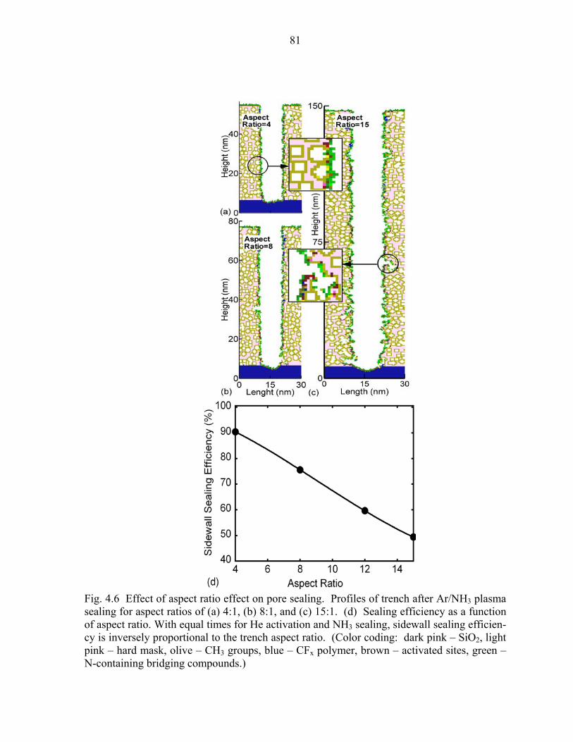
81
Fig. 4.6 Effect of aspect ratio effect on pore sealing. Profiles of trench after Ar/NH3 plasma sealing for aspect ratios of (a) 4:1, (b) 8:1, and (c) 15:1. (d) Sealing efficiency as a function of aspect ratio. With equal times for He activation and NH3 sealing, sidewall sealing efficien-cy is inversely proportional to the trench aspect ratio. (Color coding: dark pink – SiO2, light pink – hard mask, olive – CH3 groups, blue – CFx polymer, brown – activated sites, green – N-containing bridging compounds.)

82
4.6 References 1. C. M. Whelan, Q. T. Le, F. Cecchet, A. Satta, J. J. Pireaux, P. Rudlof, and K. Maex,
Electrochem. Solid-State Lett. 7, F8 (2004).
2. G. Beyer, A. Satta, J. Schuhmacher, K. Maex, W. Besling,O. Kilpela, H. Sprey, G.
Tempel, Microelectron. Eng. 64, 233 (2002).
3. T. Abell and K. Maex, Microelectron. Eng. 76, 16 (2004).
4. A. M. Urbanowicz, D. Shamiryan, A. Zaka, P. Verdonck, S. De Gendt and M. R. Bak-
lanov, J. Electrochem. Soc. 157, H565 (2010).
5. F. N. Dultsev, A. M. Urbanowicz, and M. R. Baklanov, Mater. Res. Soc. Symp. Proc.
Vol. 1079 © 2008 Materials Research Society 1079-N07-03.
6. H.-G. Peng, D.-Z. Chi, W.-De Wang, J.-H. Li, K.-Y. Zeng, R. S. Vallery, W. E. Frieze,
M. A. Skalsey, D. W. Gidley, and A. F. Yee, J. Electrochem. Soc. 154, G85 (2007).
7. K. Hamioud, V. Arnal, A. Farcy, V. Jousseaume, A. Zenasni, B. Icard, J. Pradelles, S.
Manakli, Ph. Brun, G. Imbert, C. Jayet, M. Assous, S. Maitrejean, D. Galpin, C. Monget,
J. Guillan, S. Chhun, E. Richard, D. Barbier, M. Haond, Microelectron. Eng. 87, 316
(2010).
8. G. Mannaert, M. R. Baklanov, Q. T. Le, Y. Travaly, W. Boullart, S. Vanhaelemeersch,
and A. M. Jonas J. Vac. Sci. Technol. B 23, 2198 (2005).
9. H. Seo, S. B. Kim, J. Song, Y. Kim, H. Soh, Y. C. Kim, and H. Jeon, J. Vac. Sci. Tech-
nol. B 20, 1548 (2002).
10. K. Sakuma, K. Machida, K. Kamoshida, Y. Sato, K. Imai, and E. Arai, J. Vac. Sci. Tech-
nol. B 13, 902 (1995)

83
11. M. A. Hartney, D. W. Hess, and D. S. Soane, J. Vac. Sci. Technol. B 7, 1 (1989).
12. D. Shamiryan, M. R. Baklanov, S. Vanhaelemeersch and K. Maex, J. Vac. Sci. Technol
B 20, 1923 (2002).
13. O. V. Braginsky, A. S. Kovalev, D. V. Lopaev, E. M. Malykhin, Yu. A. Mankelevich, T.
V. Rakhimova, A. T. Rakhimov, A. N. Vasilieva, S. M. Zyryanov and M. R. Baklanov, J.
Appl. Phys. 108, 073303 (2010).
14. M. Urbanowicz, M. R. Baklanov, J. Heijlen, Y. Travaly, and A. Cockburn, Electrochem.
Solid-State Lett. 10, G76 (2007).
15. Private communication with M. Urbanowicz, IMEC, Belgium, 2011.
16. M. J. Kushner, J. Phys. D 42, 194013 (2009).
17. A. Agarwal and M. J. Kushner, J. Vac. Sci. Technol. A 27, 37 (2009).
18. D. Zhang and M. J. Kushner, J. Vac. Sci. Technol. A 19, 524 (2001).
19. J. Lu and M. J. Kushner, J. Vac. Sci. Technol. A 19, 2652 (2001).
20. A. Sankaran and M. J. Kushner, J. Vac. Sci. Technol. A 22, 1242 (2004).
21. A. Sankaran and M. J. Kushner, J. Vac. Sci. Technol. A 22, 1260 (2004).
22. J. L. Bischoff, F. Lutz, D. Bolmont and L. Kubler, Surf. Sci. 251/252, 270 (1991).
23. H.-W. Guo, L. Zhu, L. Zhang, S.-J. Ding, D. W. Zhang, R. Liu, Microelectron. Eng. 85,
(2114) 2008.
24. S. Behera, J. Lee, S. Gaddam, S. Pokharel, J. Wilks, F. Pasquale, D. Graves, and J. A.
Kelber, Appl. Phys. Lett. 97, (034134) 2010.
25. M. S. Foster, A. D. Williamson, and J. L. Beauchamp, International Journal of Mass
Spactrometry and Ion physics, 15 (429) 1974.

84
5. DAMAGE BY RADICALS AND PHOTONS DURING CLEANING OF POROUS LOW-k SiOCH USING
Ar/O2 AND He/H2 PLASMAS
5.1 Introduction
The lower dielectric constant (low-k) and lower capacitance of porous materials
used for the interlayer dielectric in integrated circuits reduces signal propagation delays,
Typical low-k materials include porous SiO2 with methyl groups (CH3) lining the pores –
SiOCH. Such pristine low-k materials are essentially hydrophobic (because of the presence
of hydrophobic -CH3 groups) and do so not absorb more than a few percent of water when
exposed to air even when the humidity is high.[1] This moisture can be driven out of the
porous network by heating to 200 C without detrimentally affecting the stability of the po-
rous material.[2] However, when porous low-k SiOCH is exposed to oxygen and hydrogen
containing plasmas −CH3 groups are etched and the nature of the dielectric changes from
hydrophobic towards hydrophilic as unbonded Si atoms can adsorb water from the environ-
ment which increases the dielectric constant.[1]
Fluorocarbon containing plasmas are often used to etch SiOCH, a process that de-
posits CFx polymers on the sidewalls of the features and inside surface lining pores. Alt-
hough the polymer can effectively seal the surface pores to block moisture uptake,[1] these
CFx polymers are usually removed as they can cause compatibility issues in subsequent pro-
cessing steps. For example, halogen containing polymers can react with the diffusion barri-
er metals Ti and Ta.[3] Also, these polymers can introduce hydrophilic properties since, on
a relative basis, they are not as hydrophobic as −CHx groups.[1] It has been reported that
after a fluorocarbon etch, porous SiOCH can adsorb water from the ambient air to volume

85
fractions as high as 8%, which questions the hydrophobicity and sealing efficiency intro-
duced by CFx polymers.[1]
The removal of the CFx layer is ideally performed using an oxygen containing plas-
ma due to the efficiency of etching the polymer by oxygen radicals.[4-6] As such, O2 con-
taining plasmas have often been used for such post-etch cleaning and photoresist remov-
al.[7] However, O2 plasma cleaning can also remove hydrophobic groups (such as –CH3
from –SiO2-CH3 and –Si-H groups) from SiOCH, replacing them with hydrophilic groups
(such as –SiO2-OH) which can initiate further adsorption of H2O molecules that increases
the dielectric constant.[7-11] The presence of –SiO2-OH can result in further water uptake
by creating –SiO2-OH-H2O like compounds through hydrogen bonding.[9-11] It has been
reported that with the high dielectric constant of water (k ≈ 80), loss of hydrophobic –CH3
groups and incorporation of water from humid air can increase the dielectric constant k from
2.5 to 20 within 10 minutes of O2 plasma treatment.[2]
The hydrophilic nature of SiOCH has a nearly linear relationship with carbon deple-
tion.[1] As a result, a cleaning process that minimizes C depletion will also help to maintain
the hydrophobic properties of the film. SiOCH is relatively stable when H2 plasmas are used
for cleaning compared to the use of Ar/O2 plasma cleaning.[12] The addition of He to the H2
plasma aids in preconditioning the surface to improve pore sealing in subsequent treatment
using NH3 containing plasmas.[13-15] It has also been reported that He/H2 plasmas are an
attractive option for photoresist (PR) mask removal due to there being a small increase of the
dielectric constant of low-k films during the ashing process.[16]
These processes are complicated by the presence of VUV radiation from the plasma
coincident to the fluxes of radicals and ions. VUV photons can produce scission of nearly all
86
bonds in the SiOCH films and of Si-C bond in –SiO2-CH3 in particular. Such bond scission-
ing has the potential of accelerating damage by generating sites that react with plasma pro-
duced species at locations that would otherwise be nonreactive with the same species. These
sites are more likely to react with or hydrogen bond with water, which further increases the
dielectric constant.
In this chapter, we discuss reaction mechanisms and computationally analyze damage
of porous SiOCH during cleaning with Ar/O2 and He/H2 plasmas when considering the con-
sequences of VUV photon fluxes from the plasma. The Hybrid Plasma Equipment Model
(HPEM) was used to obtain the ion energy and angle distributions of reactive fluxes from
inductively coupled plasmas with capacitive substrate biases for cleaning, and from capaci-
tively coupled plasmas for etching.[17] These distributions were then used as input to the
Monte Carlo Feature Profile Model (MCFPM) to predict profiles and composition of the Si-
OCH.[18] Damage of the porous SiOCH was characterized by the depth at which removal of
−CH3 is observed – the demethylation depth. For pores which are not in the line-of-sight to
the plasma, diffusion of reactive species into the porous SiOCH is required for damage to
occur in the absence of VUV photons. We have also found that deeply penetrating plasma-
produced-photons can produce Si-C bond scissioning which accelerates the removal of –CH3
groups. Results will be discussed for the cleaning of pores as a function of treatment time,
interconnectivity, and photon fluxes.
In Chapter 6, we concentrate on degradation or increase in dielectric constant result-
ing from water incorporation after the cleaning damage.[19] –CH3 groups are etched from –
SiO2-CH3 during cleaning and such removal generates –SiO2• which has a dangling bond.
Water attacks such site and form –SiO2-OH type products. For the high k (≈80) of water,

87
such products have a high k and it increases the overall k of the porous low-k. In Chapter 6,
we model the degradation of k as a function of water volume incorporation in the porous
SiCOH. O2 plasmas for its aggressive etching nature remove more −CH3 groups and will
cause more water adsorption from air after the damage compared to He/H2 clean. As such,
Ar/O2 clean is more harmful to the low-k in terms of preservation of low-k integrity, than
He/H2 clean.
The reaction mechanisms for plasma damage of SiOCH are discussed in Sec. 5.2, fol-
lowed by a discussion of plasma properties in Sec. 5.3. Removal of hydrophobic −CH3 and
its dependence on interconnectedness, porosity and photon fluxes is discussed in Sec. 5.4.
Consequences of VUV photon fluxes are discussed in Sec. 5.5 and a comparison of our com-
puted trends with prior works is discussed in Sec. 5.6. Our concluding remarks are in Sec.
5.7.
5.2 Surface Reaction Mechanisms
A reaction mechanism was developed for plasmas sustained in He/H2 and Ar/O2
mixtures and their interactions with low-k porous SiOCH. The HPEM was employed to ob-
tain the energy and angular distributions for charged and neutral species incident onto the
surface.[17] The HPEM has been previously described and so is only briefly summarized
here. The HPEM is a two-dimensional, modular model which addresses gas phase and sur-
face kinetics. Electromagnetic fields are derived by solving the frequency domain wave
equation based on coil currents adjusted to deliver a specified power deposition. The spatial-
ly dependent power deposition is used as a source term in obtaining the electron temperature,
Te, from an electron energy conservation equation. Transport and rate coefficients as func-
88
tion of average electron energy are obtained from a solution of Boltzmann’s equation, and a
Monte Carlo simulation is used to follow the trajectories of sheath accelerated secondary
electrons. The transport coefficients and source functions are used by the fluid kinetics mod-
ule (FKM) to solve separate continuity, momentum, and energy equations for each ion and
neutral species, while semi-implicitly solving Poisson’s equation for the time varying elec-
trostatic potential. The densities and electrostatic fields from the FKM are then transferred to
the other modules. This process is iterated until a converged quasi-steady state solution is
obtained.
Reaction probabilities for gas phase species with surfaces are provided by the surface
chemistry module (SCM) which computes the composition of surface resident species using
a multilayer surface-site-balance model. The reaction mechanism is unique for each surface
in contact with the plasma. The plasma chemistry Monte Carlo module (PCMCM) produces
the energy and angular distributions for neutrals and ions striking surfaces in contact with the
plasma. The PCMCM launches pseudo-particles representing ions and neutrals based on the
electron impact source functions. Using time dependent electric fields from the FKM, their
trajectories are integrated while accounting for gas phase collisions. The energy and angular
distributions (EADs) of neutral and ion pseudo-particles are recorded as they strike surfaces.
The SCM and MCFPM incorporate energy dependent reaction probabilities based on
the EADs obtained from the PCMCM. The probabilities for surface reactions involving en-
ergetic species (either ions or hot neutrals) are given by [17]
p(E) = p0 mt
mr
mt
m
EEEE
−− (5.1)
where p(E) is the reaction probability for a particle with energy E, Et is the threshold energy

89
of the process, Er is a reference energy, and po is the reaction probability at the reference en-
ergy. We used m = 0.5 in this work.
The Monte Carlo Radiation Transport Module (MCRTM) in the HPEM is called after
each iteration to provide photon fluxes incident onto the SiOCH.[18] The operation of
MCRTM is similar to the operation of PCMCM. Source functions for launching of pseudo-
particles representing photons are derived from the excited state densities generated by the
FKM. The trajectory of a photon is tracked until it is absorbed by a gas phase species or it
strikes a surface. The photon absorption probability is obtained from a Voight line-shape
function using the natural lifetime, collisional broadening and Doppler broadening produced
by the local gas densities and temperatures. If resonantly absorbed, photons are re-emitted
using a partial-frequency redistribution algorithm. The fluxes and spectra of photons are rec-
orded as a function of the material the photons strike, and are exported to the surface kinetics
module SCM of the HPEM. The rates of photon absorption and re-emission are recorded for
each optical transition, and are used to calculate radiation trapping factors which lengthen the
natural lifetime of the emitting species. These factors are exported to the FKM.
The damage mechanism for SiOCH to be discussed below was implemented in the
MCFPM with which the evolution of the SiOCH and damage are predicted.[20] The
MCFPM resolves the porous material with approximately atomic resolution. The numerical
cell size in this work is 0.4 nm × 0.4 nm, which is an effective radius of 0.2 nm. The creation
of pores in the MCFPM mesh is discussed in Ref. [21]. The internal surfaces of the pores in
SiO2 were lined with a single layer of -CH3 to approximate the structure of SiOCH.
Using the angular distribution of fluxes provided by the MCRTM, the MCFPM then
addresses photon penetration into the SiOCH. In principle, the MCFPM treats photons simi-

90
larly to radicals or ions. Based on the magnitude and angular distribution of photons of dif-
ferent wavelengths, a pseudoparticle representing a photon is randomly directed towards the
substrate. For each material in the mechanism an absorption length is specified. The proba-
bility that a photon m will be absorbed by material j crossing cell i is ( )imjimjp lλexp1−= ,
where mjλ is the absorption length in material j for photon m and il is the traversal distance
of the photon across the cell i. When a photon enters into a material cell, this probability is
evaluated. If r ≤ pimj, where r is a random number distributed on (0, 1), the photon is ab-
sorbed. Otherwise, the photon continues along its trajectory. When absorbed, the material
identity of the solid cell is changed based on the reaction mechanism.
For the Ar/O2 plasmas of interest, the UV and VUV fluxes are dominated by emission
from oxygen species.[22] Electron impact excitation of O atoms generates O(3s), O(5s), and
O(5p) states. The O(3s) emits 130 nm photons and O(5s) emits 136 nm photons in relaxing
to ground state. O(5p) also emits 777 nm photons in relaxing to O(5s). To simplify the reac-
tion mechanism in the MCFPM we considered only radiation transport into solid materials of
the 130 nm photons. The penetration distance of 130 nm photons into porous SiOCH is λ
≈100 nm.[23-25] In low pressure He/H2 plasmas, damaging VUV fluxes are dominated by
resonance radiation from He(21p) at 58.4 nm having a penetration depth of ≈20 nm in the po-
rous SiOCH.[13, 24] The damage mechanisms of these VUV photons are dominantly bond
breaking. For example, the 130 nm and 58.4 nm photons have enough energy to break both
Si-C and Si-O bonds. In the former case, the dissociated •CH3 remains physisorbed. In the
latter case, the Si-O is converted to a free radical site (denoted as SiO2* here).

91
It is believed that reactions of O radicals with CH3 groups of SiOCH are the primary
mechanism for C depletion during Ar/O2 plasma processing of porous low-k films.[8,26]
With interconnected porous SiOCH, oxygen atoms can diffuse into the porous network and
react with the hydrophobic −CH3 groups in –SiO2-CH3 located on the pore-walls well below
the surface.[27] The carbon in the –CH3 groups is likely removed as CO or CO2.[27-29]
Reactions of O atoms can also abstract H from –SiO2-CH3 leaving –SiO2-CH2.[27] O radi-
cals having an energy >0.1 eV can break the Si-C bond of –SiO2-CH2 that eventually leads to
the formation of CO and H2O leaving behind an unpassivated Si atom on the surface of the
pore.[26,27] Si-C bond scission in –SiO2-CH3 by VUV photons, leaves behind adsorbed
•CH3 which can be later etched by O atom.[23,25,26] We note that O2 plasmas do not sig-
nificantly etch SiO2, and so their primary reactions are with the carbon contained in CH3
groups.[28]
The probabilities in the following reactions for both surface site modification and –
CH3 etching in Ar/O2 and He/H2 plasmas have been determined by extensive parameteriza-
tion of the models to be qualitatively consistent with experimental results available in the lit-
erature. Bounds of reaction probabilities are set based on thermodynamic properties and the
change in enthalpy of reactions. Within those bounds parameterization and comparison to
experiments refine the mechanism. Some examples of works that guided the development of
the reactions are discussed in Sec. 5.6.
The reactions for removal of –CH3, or demethylation of SiOCH, in plasmas contain-
ing O2 are listed in Table. 5.1.[23, 25-29] In these mechanisms, the subscript g denotes a gas
phase species, subscript a denotes an adsorbed species, the number of symbol • represents
number of dangling bonds or free radical site, and – (or =) represents bonding to the solid.

92
(A complete reaction mechanism consisting of many hundreds of reactions can be obtained
by request from the authors.)
Oxygen radicals, O, can directly and exothermically reaction with –SiO2-CH3 through
H abstraction to form OH and a free radical site, or O atoms with energy > 0.1 eV can pro-
duce Si-C bond scission as suggested in Ref. [26], in turn producing •CH3a on the surface.
Both of these outcomes are vulnerable to further O radical or O2 attack that eventually re-
move methyl groups. To etch –CH3 groups in Ar/O2 plasmas, Si-C bond breaking caused by
VUV photons is not essential. However, if photons are present, Si-C bond scission occurs
which can accelerate removal of –CH3 groups. Etch products of such –CH3 removal reac-
tions include CO, CO2 and H2O. Such internally generated H2O during –CH3 etching can
react with –SiO2• sites forming –SiO2-OH which can contribute to an increase in the dielec-
tric constant.
He/H2 plasmas remove −CH3 groups from SiOCH at a slower rate compared to O2
containing plasmas primarily due to the higher threshold energies for these reactions involv-
ing H atoms. In addition, the reactions responsible for −CH3 removal in He/H2 plasmas like-
ly produce less volatile products, such as CH4, which are less likely to continue reacting with
the SiOCH. He plasma pretreatment of SiOCH has been found to produce surface modifica-
tions that can minimize damage of the low-k.[13-15] He+ and photons from He/H2 plasmas
can remove H from the -CH3 groups of –SiO2-CH3 producing –SiO2-CHn (n = 0-2) that have
lower etch rates. This is because H is only efficient in removing C from –SiO2-CH3 among
all –SiO2-CHn(n = 0-3) products as volatile CH4. Since the activation energy to remove C
from –SiO2-CH3 increases as n decreases, the rate of C removal from –SiO2-CHn by thermal
H atoms decreases as H is removed. Although hot H atoms are able to produce this etching,

93
H* are only energetically above threshold near the surface. By the time H atoms diffuse into
the pores, their energy has largely been thermalized to below the threshold energies required
to etch –SiO2-CHn (n < 3). To etch these compounds, they would first need to be saturated
back to –SiO2-CH3 through H adsorption, followed by H atom etching –CH3 as volatile CH4.
The end result is that generation of –SiO2-CHn(n<3) by photons or ions could slow –CH3 re-
moval.
In certain parameter spaces of operating of low pressure He/H2 plasmas, it is possible
to produce significant fluxes of hot H atom fluxes to the substrate. The dominant mechanism
for hot H generation is the dissociation of vibrationally excited H2(v ≥ 2) by electron impact.
Such reactions can generate H atoms with energies sufficient to remove both CFx polymers
and PR. Charge exchange reactions between H2(v) and H+, or H+ and H can generate H at-
oms and H2 with energies as high as the energy of H+. Such charge exchange reactions also
occur between H2(v ) and H2+ producing translationally hot H2(v). Vibrational-translational
(VT) reactions of H atoms with H2(v) also can produce hot H. In these collisions, H2(v) mol-
ecules are relaxed to a state H2(v’<v), and the H atoms carries away the energy difference as
translational energy. A more detailed hot H generation mechanism is discussed in Sec. 5.3.
Hot H atoms in this context have translational energies of up to or exceeding a few
tenths of an eV. H atoms with energies > 0.4 eV are able to abstract H from –SiO2-CH3 pro-
ducing –SiO2-CHn (n =1, 2) which slows the rate of carbon removal. Cleaving of Si-C bonds
by photons produces adsorbed •CH3a groups that can be later etched by H atom as
CH4.[13,14,29] After –CH3 removal from –SiO2-CH3, H atoms can passivate the resulting –
SiO2• site by forming –SiO2-H which is hydrophobic in nature and can also block subsequent
water update.[30] However, He+ can break Si-O bond in −SiO2• and generate free radical site

94
−SiO••, and a successive strike can produce −Si•••. H can passivate −Si••• forming −Si-Hn
(n= 1-3). Such Si-H bond compounds are also hydrophobic in nature and can block water up-
take. As such, even after the -CH3 group removal, He/H2 plasma treatment may be able to
maintain some hydrophobic properties of the SiOCH.
Reactions during interaction between He/H2 plasmas and SiCOH are listed in Table
5.2.[13,14,25,29,30] Among these reactions, H reactions that involve removal of –CH3
groups or demethylation (Reactions 6 and 13) and abstraction of H from –CHn (x=1-3) (Re-
actions 15-35) are endothermic, and require hot H atoms or vibrationally excited H2 to quick-
ly proceed. However, −CH3 removal reactions are less endothermic than H abstraction reac-
tions and H passivation of –SiO2-CHn. −Si••• and −Si-Hn (n=1, 2, 3) reactions with H (Re-
actions 10-12) are exothermic in nature.
PR which is dominantly a hydrocarbon, can be removed by O atoms from Ar/O2
plasmas by forming compounds such as CHO, while hot H atoms (> 0.5 – 1 eV) and vibra-
tionally excited H2(v>2) produced in He/H2 plasmas can remove PR by forming compounds
such as CH4. O containing ions such as O+ and O2+ can etch PR as CHO. H containing ions
H+, H2+ and H3
+ chemically etch PR as CH4. Energetic ions such as Ar+ and He+ can physi-
cally sputter PR. The mechanism for removal of PR in Ar/O2 and He/H2 plasmas is listed in
Table 5.3. PR etching reactions that involve O species (Reactions 1-3) are exothermic. H
atom or H2(v>3) etching reactions (Reactions 4-10) are endothermic. SiO2* (bond cleaved
SiO2) which is generated by VUV photons are not believed to be chemically active in H2 or
O2 plasmas. It has been reported that SiO2* can only adsorb O in Ar/O2 plasmas forming a
SiO2 like layer (without showing any etching of SiO2).[29] Similarly, H is adsorbed by SiO2*
without causing any Si consumption in He/H2 plasmas. Given these trends, since the empha-

95
sis of this study is on demethylation, we excluded SiO2* reactions in Ar/O2 or He/H2 plasmas
for simplicity.[29,31]
5.3 Plasma Properties
For purposes of this investigation, plasma cleaning processes were modeled as per-
formed in inductively coupled plasmas. The test reactor treated a wafer 15 cm in diameter.
The reactor was 26 cm in diameter with a wafer-to-coil height of 10 cm. (See Fig. 5.1a.)
The conditions for both Ar/O2 and He/H2 plasma treatment were 10 mTorr with a flow rate of
100 sccm. For the base case, the coil delivered 300 W at 10 MHz with a pressure of 10
mTorr and flow rate of 100 sccm. The gas mixtures were He/H2 = 75/25 and Ar/O2 = 5/95.
The substrate was biased with at 10 MHz
Typical plasma properties for a power of 300 W are shown in Fig. 5.1 and reactive
fluxes to the substrate are shown in Fig. 5.2. For Ar/O2 plasmas, the peak O-atom density is
9.5 × 1013 cm-3 and the peak total ion density is 6 × 1011 cm-3. O(3s), which emits 130 nm
photons, has a peak density of 3.5 x 107 cm-3, a small density due to its short radiative life-
time that produces, when integrated over the reactor, reasonably large VUV fluxes to the
substrate. With a 20 V substrate bias, ions have an average energy near 30 eV and a total
flux of 2.3 × 1016 cm-2s-1 at the center of the wafer. The individual fluxes include 1.5 × 10¹⁶
cm-2s-1 for O+, 0.6 × 1016 cm-2s-1 for O2+, and 2.1 × 1015 cm-2s-1 for Ar+ . O atoms, the domi-
nant agent for −CH3 removal, has a flux of 1.5 × 1018 cm-2s-1. The flux of VUV photons is
2.5 × 1013 cm-2s-1.

96
In He/H2 plasmas, the peak ion density is 3.5 × 1010 cm-3 while H atoms have a max-
imum density of 1.8× 1013 cm-3. The ion fluxes (1.8 ×1016 cm-2s-1) largely responsible for the
PR removal had an average energy near 30 eV for a 20 V bias and an angular spread from the
vertical of < 150. He(21p) which emits 58.4 nm photons has a peak density of 1.5 x 108 cm-3.
The individual fluxes include 4 × 1015 cm-2s-1 for H+, 7× 1015 cm-2s-1 for H2+, 1× 1015 cm-2s-1
for H3+, and 6× 1015 cm-2s-1 for He
+. The VUV flux is 6 × 1014 cm-2s-1 and that for H atoms is
1× 1018 cm-2s-1.
Hot H atoms (H*) have temperatures (or energies) that exceed that of the average gas
temperature. The EADs of H atoms incident onto the wafer are shown in Fig. 5.3 for He/H2
mixtures for pressures of 10-80 mTorr. H* fluxes to the wafer are also shown as a function
of pressure. The EADs are dominated by a thermal isotropic component corresponding to
the gas temperature of ≈800 K. At lower pressures, a significant population of H* is pro-
duced, in general also having an isotropic angular distribution. As the pressure increases, the
fraction of H* decreases, however, its angular distribution narrows.
The dominant H* generation mechanism is by Frank-Condon heating through the dis-
sociation excitation of H2(v ≥ 2) by electron impact.[32] Although such reactions cannot
generate H atoms with energies >4 eV, the energy is sufficient to initiate endothermic poly-
mer cleaning or PR removal reactions. Charge exchange reactions between H2(v ) and H+, or
H+ and H can generate H atoms with energies as high as the energy of H+ ions in the plasma.
Charge exchange reactions can also occur between H2(v ) and H2+ producing translationally
hot H2(v ) having sufficient energies to initiate endothermic polymer cleaning or PR etching

97
reactions. As the rate of charge exchange is small compared to dissociative excitation, a
small fraction of H* is produced in this manner.
H* can also be produced through vibrational-translational (VT) reactions of H atoms
with H2(v).[33] In these collisions H2(v) molecules are quenched to a state H2(v’ < v), and
the H atoms carries away the energy difference as translational energy, 0.5 eV per vibrational
level. These VT reactions can give H atoms enough energy to broach the endothermic barrier
to clean CFx polymer or PR.
Optimizing the collisionality of He/H2 plasmas by changing pressure enables a high
rate of H* production while also allowing these H* to reach the wafer. The total H atom
flux, and fluxes of H atoms with energies >0.5 eV and >1 eV as a function of pressure are
shown in Fig. 5.3b. For pressures >20 mTorr the H* fluxes decrease in large part due to
thermalization of initially produced H* before those atoms reach the surface. With an in-
crease in pressure from 10 mTorr to 200 mTorr, total H flux rises from 1018 to 1019 cm-2s-1
while the energy of H atoms decreases. At 10 mTorr, roughly 1% of the H atoms have ener-
gies >0.5 eV which is above the threshold energy to etch PR and remove CFx polymers. At
30 mTorr, only 0.1 % of H atoms have energies >0.5 eV. At pressures of >80 mTorr, the
fraction of H atoms with energy >0.5 eV is only 0.006%. Since H* fluxes are required to
efficiently remove the CFx polymer that remains on trench sidewalls after fluorocarbon plas-
ma etching, operating at pressures of less than tens of mTorr is preferred.
5.4 Demethylaton
For the base case the pore size is 0.8 nm in diameter with a 10% standard deviation
and the porosity is 30% with 100% interconnected pores. –CH3 groups initially line the pore-
98
walls. The calculated dielectric constant is approximately k = 2.5, based on the relationship
between film dielectric constant, and volume of each element in the porous film (CH3 group,
SiO2 and air gap) and their individual dielectric constants.[34]
Trenches were etched into SiOCH with a capacitively coupled plasma using an
Ar/C4F8/O2 = 80/15/5 gas mixture at 40 mTorr.[20,35] The end result of the etching includes
a CFx polymer layer, approximately 1.5 nm thick, on the etched SiOCH surface, as shown in
Fig. 5.4a. The simulation was run for a sufficiently long time to completely erode the PR
mask to investigate the damage during the cleaning step. The trench profile following 850s
of treatment by the Ar/O2 plasma is shown in Fig. 5.4b. Damage in these profiles is inter-
preted primarily as the removal of -CH3 (demethylation) and to a secondary degree by the
formation of SiO2*. In this Monte Carlo based model, the removal of −CH3 from the inside
of pores results in the appearance of an increase in the pore-size, as a layer of molecules have
been removed from the surface of the pore. In reality, there is likely a collapse of the pores, a
process that is not resolved in these simulations.
The mask and polymer are essentially fully removed during the cleaning process. We
found that demethylation (removal of −CH3 groups from –SiO2-CH3 in porous SiOCH) is a
diffusion dominated process, as suggested by Goldman et al.[8] The maximum depth of de-
methylation increases linearly with time at short times and scales with t1/2 at longer times, as
shown in Fig. 5.4c.[8] Pores which are open or line-of-sight connected to the plasma have
their –CH3 groups more rapidly removed by photons, ions and O radicals. Interconnected
pores deeper into the material are demethylated only after diffusion of O atoms through the
porous network and, if near the surface, catalyzed by VUV bond scission.

99
VUV Photons have a finite penetration depth into solid SiO2. Photons that are ab-
sorbed by −SiO2-CH3 likely produce Si-C bond scission, which then produces free radical
sites, −SiO2• and bond cleaved and surface adsorbed •CH3a. These sites speed the demethyl-
ation process, as discussed below. Bond cleaved •CH3a can be etched by O as CO and H2O,
and can be removed by H radicals as CH4. In these situations, even O2 can promote such
demethylation once the Si-C bond has been broken and •CH3a produced.[23] One of the
products of O-atom reactions with –SiO2-CH3 and •CH3a is OH, which can itself react with
SiOCH, which tends to perpetuate the demethyation process.[27]
For both Ar/O2 and He/H2 plasmas photon fluxes increase with power as shown in
Fig. 5.5. The VUV photon fluxes from Ar/O2 plasmas are 10-100 times smaller than for
comparably powered He/H2 plasmas. To decouple heavy particle kinetics and photon fluxes
in the assessment of demethylation, we held the heavy particle fluxes constant at their base
case values and varied the fluxes of VUV photons. As the photon fluxes increase so does the
demethylation depth, shown in Fig. 5.5c for a treatment time of 900 s. Since O atoms are
exothermically reactive with SiOCH there is significant demethylation even in the absence of
VUV fluxes for Ar/O2 plasmas. For He/H2 plasmas, there is little demethylation in the ab-
sence of VUV fluxes. In both cases, increasing the VUV fluxes increases the amount of Si-C
scission in –SiO2-CH3 (producing either •CH3a or –SiO2-CH2•), which enables more rapid
reactions which lead to demethylation. The demethylation depth increases linearly with pho-
ton flux up to about 1014 cm-2s-1 and then increases with flux1/2 for the range 1014-1015 cm-2s-
1. This dependence is similar to diffusion limited damage, as suggested by the results in Fig.
5.4c.[8,24] The demethylation depth increases to nearly 30 nm in the Ar/O2 plasma with in-

100
creasing photon flux for fixed exposure time (or increasing fluence) and up to 11 nm in the
He/H2 plasma.
To compare the impact of VUV photons on damage of the SiOCH, the top layer of
SiOCH is shown in Fig. 5.6 for Ar/O2 plasma cleaning and in Fig. 5.7 for He/H2 plasma
cleaning without photons and with increasing photon fluxes. The demethylation is represent-
ed by the depth of removal of (olive colored) –CH3 groups after plasma treatment. The
change in color from pink (SiO2) to purple represents the formation of SiO2*, the free radical
state of SiO2 due to Si-O bond breaking by photons. Although SiO2* can be etched in plas-
mas containing Cl and F radicals, radicals produced in Ar/O2 or He/H2 plasmas generally do
not react with SiO2* as etchants though these plasmas may passivate the free radical
site.[29,31] As Worsely et al. suggested, Ar/O2 plasmas can remove the entire carbon con-
tent from SiOCH but do not remove SiO2 and leave a SiO2 like layer.[29] On the other hand,
He/H2 plasmas less aggressively remove carbon but leave SiO2 primarily unaffected with on-
ly some H incorporation.
Increasing VUV fluxes increases the depth of demethylation and also increases the
proportion of SiO2* sites. Although many of these free radical sites likely reconnect to re-
form SiO2 without long term damage to the SiOCH, some fraction of SiO2* also likely re-
mains in the long term, making the SiOCH more sensitive to damage in other processing
steps. Note that in those regions of the SiOCH where, statistically, there are more pores and
so more damage, the VUV penetration depth is greater. This is due to there being more line-
of-sight pathways for the photons to penetrate or there being smaller line averaged mass den-
sity.

101
The demethylation depth is larger for flat surfaces than for the sidewalls, as shown in
Fig. 4b. This is due, in part, to the additional role that directional ions and photons play in
the demethylation process. Due to their either line-of-sight reactivity or anisotropic trajecto-
ries, ions and photons make larger contributions to demethylation to horizontal surfaces than
vertical surfaces. The average angle of incidence of ions and photons is more normal on the
flat surfaces, and so the penetration is deeper perpendicular to the surface. Finally, there is
also a time-lag issue. Additional time is required by O atoms, the dominant demethylation
agent, to statistically enter into pores at the bottom of the trench where their fluxes are small-
er than on the top surfaces, which may result in a reduced demethylated depth.
As the interconnectivity of the SiOCH increases, there are, on the average, longer av-
erage pathways from the surface for the diffusion of plasma produced species into the Si-
OCH. This ultimately produces more damage (demethylation) in the porous material com-
pared to a smaller interconnectivity.[8] For example, demethylation depth as a function of
interconnectivity during Ar/O2 and He/H2 plasma cleaning is shown in Fig. 5.8 after 900 s of
treatment. For both without and with photons, demethylation depth increases nearly linearly
with interconnectivity. The increase in interconnectivity for a given porosity increases the
likelihood of having a line-of-site path through the porosity from the plasma. Even though
photon penetration on the average should depend only on porosity (or the average mass den-
sity), statistically, increasing porosity does increase the likelihood of having pores aligned
that enable deeper photon penetration. We did find that the maximum photon penetration
depth increases with interconnectivity, as shown in Fig. 5.8c. The deeper photon penetration
then facilitates greater rates of demethylation deeper into the SiOCH. As a result, damage is
more sensitive to interconnectivity when including photon fluxes. Since a reasonable large

102
porosity (≈20-30%) is achieve a low k-value, minimizing interconnectivity can be helpful in
minimizing the damage of the network.[8]
SiOCH profiles for interconnectivities of 10, 40 and 100% for following treatment
with Ar/O2 and He/H2 plasmas are shown in Figs. 5.9 and 5.10. (The penetration depth of
photons is shown by the change in color: brown –CH3 groups turn green after photon pro-
duced Si-C bond scission, and light pink SiO2 turns dark pink to represent SiO2*). During
He/H2 plasma cleaning, reactive H atoms also diffuse inside the material through intercon-
nected pathways. Although H atoms being lighter than O atoms can diffuse more rapidly and
so possibly deeper into the SiOCH, reactions of H atoms with SiOCH are slower and produce
less volatile and reactive products than reactions with O atoms.[12,29] So for otherwise
identical conditions, diffusion of O atoms through interconnected pores will produce more
damage than diffusion of H atoms.
The demethylation process is facilitated by Si-C bond scission by VUV photons. In
Ar/O2 plasmas, demethylantion by O atoms is an exothermic process. As a result, demethyl-
ation is enhanced though not dependent on bond scission by VUV photons. The profile of
demethylzation is therefore more diffusive, a consequence of O atoms diffusion into the
pores. In He/H2 plasmas, Si-C bond scission significantly enhances the rate of demethyla-
tion, and so its depth is more closely correlated to that of the photon penetration. As a result,
the demethylation depths as a function of interconnectivity in He/H2 plasma are approximate-
ly 3 times smaller than in Ar/O2 plasmas.
Increasing porosity increases the depth of damage in SiOCH as shown in Figs. 5.11
for porosities of 30% and 40% in Ar/O2 plasmas. We found that the depth of damage in-
creases nearly linearly with porosity as shown in Fig. 5.11c.[1,29] At first glance, a more

103
porous network should enable more rapid diffusion of radicals throughout the volume of the
SiOCH and so increase the likelihood of damage at a deeper site. There is a secondary effect
of photon transport – the less dense the SiOCH due to increasing porosity, the longer the
penetration depth of photons due to the lower mass density of the material. These results are
not independent of interconnectivity, as discussed below.
5.5 Consequences of VUV Photon Fluxes
VUV photons from Ar/O2 and He/H2 plasmas penetrating into SiOCH produce Si-C
bond scission which generates •CH3a radicals on the surface of pores. These photons also
produce SiO2* through Si-O bond cleavage.[23-25] These Si-C bond cleaved •CH3a groups
are thought to remain as adsorbed surface species.[23] Since the •CH3a groups are no longer
chemisorbed, they are vulnerable to rapid reaction with O, O2 or H to produce volatile CO,
CO2 or CH4 to complete the -CH3 removal process. Molecular oxygen is unable to etch –
CH3 when bonded to Si, however after Si-C bond cleavage, •CH3a is etchable by O2 ultimate-
ly producing CO and H2O.[23] Fluxes of VUV photons from plasma can therefore signifi-
cantly increase the rate of demethylation compared to fluxes of only O or H atoms. The 130
nm photons from O atoms in Ar/O2 plasmas have a penetration depth of ≈100 nm into Si-
OCH and so can increase demethylation to at least this depth provided the interconnectivity
enables penetration of plasma produced radicals into the network.[23,25] The 58 nm photons
produced by He* in He/H2 plasmas have penetration depths of only ≈20 nm, and are energet-
ic enough to break both Si-O and Si-C bonds.[24] Due to the less reactive nature of H radi-
cals with –SiO2-CHx groups, Si-C bond cleavage by photons from He/H2 plasmas is a more
important precursor to the removal of hydrophobic –CH3 groups by H atoms than oxygen

104
containing plasmas where the carbon removal step is exothermic.[25]
The depths of demethylation shown in Figs. 5.6 and 5.7 as a function of photon flux
are consistent with experimentally measured ranges of damage of SiOCH for photon fluxes
of 1014-1015 cm-2s-1.[25] Damage of the SiOCH increases in depth as the photon fluxes in-
crease. This is in large part due to saturation of the scission of the Si-C bonding in –SiO2-
CH3. The maximum demethylation depth is to a large degree determined by the penetration
depth of the particular wavelength into the SiOCH. The actual demethylation depth is then
determined by the degree of Si-CH3 scission within that maximum depth. In some ways,
damage is a matter of fluence of photons (photons/cm2) as opposed to simply flux (pho-
tons/cm2-s). A longer treatment time for a given flux of photons will produce a deeper de-
methylation. Damage of SiOCH for the same fluence of VUV photons (keeping VUV pho-
ton flux × time= constant) is shown in Fig. 5.12 for He/H2 and Ar/O2 plasma cleans. With
the same fluence, SiOCH was treated in Ar/O2 plasmas with photon fluxes of 5 × 10¹⁴ and
1015 cm-2s-1. The amount of Si-C bond scission was essentially the same in both cases.
However, O radicals had twice the time to diffuse into the network for the lower photon flux,
and so produced somewhat deeper damage. Similarly, in He/H2 plasmas for equal photon
fluence, H radicals having more time to diffuse into the network caused more damage to the
SiOCH with the lower photon flux.
Fluorocarbon plasma etched trenches in porous SiCOH producing CFx polymer cov-
ered sidewalls were cleaned in Ar/O2 and He/H2 plasmas. The resulting profiles are shown in
Fig. 5.13 with and without photon fluxes. During the over-etch required to remove all of the
CFx polymers, O2 containing plasmas caused significant demethylation by removing −CH3
groups. (Damage is shown as pink sites indicating a SiO2 site that has lost −CH3). On the

105
other hand, H radicals remove −CH3 less aggressively in large part because hot H atoms are
required for efficient removal of −CH3, and as H atoms diffuse into the pores, they thermal-
ize and so lose reactivity. In the absence of VUV illumination, He/H2 may clean porous
SiCOH without causing significant damage, only modifying the surface which sees larger
fluxes of hot H atoms, as suggested by others.[12,16]
However, with 58 nm photon fluxes in He/H2 plasmas, the resulting Si-C bond scis-
sion enables damage, both on the sidewalls and on the top of the feature. Due to the grazing
view-angle to the plasma deep in the trench, the depth of the damaged layer due to photon
absorption perpendicular to the surface is less than on the top of the feature. As the absorp-
tion length of the photons produced in Ar/O2 plasmas is longer than in He/H2 plasmas the
extent of the damage perpendicular to the sidewalls is correspondingly thicker. During
He/H2 plasma cleaning, Si-C bond scission which causes the removal of –CH3 from Si-CH3
as CH4 eventually leads to the formation of hydrophobic =Si-Hx which additionally protects
the Si from moisture adsorption. [29]
5.6 Comparison of Trends With Prior Works
As reported by Goldman et al. [8] and, Vanstreels and Urbanowicz [16], we found
that diffusion of O atoms is the dominant process for producing damage by Ar/O2 plasmas in
porous SiOCH. We also found that, as suggested by Jinnai et. al. [25], and Lee and Graves
[23] scission of Si-C bonds by VUV fluxes can increase the rate of damage. We found that
in the absence of VUV fluxes, He/H2 plasmas modify the low-k surface but do not efficiency
remove C atoms which agrees with reports that found little damage in SiOCH after pro-
cessing in a downstream He/H2 plasma reactor where the flux of VUV photons is negligi-

106
ble.[12,16] However, the 58 nm photons produced in He/H2 plasmas can cause Si-C bond
scission and so likely act as a precursor to damage, as concluded by Jinnai et al.[25] We
found that the depth of damage (−CH3 removal) for Ar/O2 plasma treatment when treated for
the same duration is approximately 3 times larger than He/H2 plasma cleaning. These results
align with those reported by Worsley et al.[29], albeit for plasma damage produced in a ca-
pacitively coupled system. They found deeper damage of SiOCH in Ar/O2 mixtures com-
pared to Ar/H2 mixtures but deeper non-damaging modification in Ar/H2 mixtures, perhaps
due to the higher mobility of H atoms in the SiOCH. They also found etch rates and the rate
of carbon removal were significantly higher in the Ar/O2 plasmas due to the highly reactive
O atom fluxes. Based on the ∆H of the reaction, Worsely et al. estimated that CH3 removal
by O atoms is more than two times energetically favorable compared to removal by H atoms.
[29]
5.7 Concluding Remarks
Ar/O2 and He/H2 plasma damage of porous SiOCH was investigated and mechanisms
discussed. While diffusion of radicals into the network is likely the primary cause for dam-
age of porous SiOCH, the presence of photons can accelerate the rate of damage. Plasmas
that can remove –CH3 by virtue of exothermic reactions will cause more damage to SiOCH
than plasmas that remove such groups relying on endothermic reactions, and this in large part
explains the higher damage potential of Ar/O2 plasmas compared to He/H2 plasmas. The
wavelength of photons present in the plasmas is important as the penetration depth of pho-
tons increases with wavelength in the VUV and deep UV, and energies of photons decrease
with wavelength. Photons having wavelengths <140 nm have enough energy (>9 eV) to

107
cause Si-C and Si-O bond scission and play a major role in the damage of SiOCH. The in-
terconnectivity of the pores enables radicals to etch methyl groups deep in the SiOCH by dif-
fusing through the network. If pores are relatively isolated (less interconnected), reactive
species will not find a well-connected path to diffuse and remove –CH3 groups located on
deeper pore-walls. As such, SiOCH with low interconnectivity, cleaned by a plasma produc-
ing fluxes containing small fractions of O atoms and producing photons which do not pene-
trate deeply into the material may be a way to maintain low-k integrity.
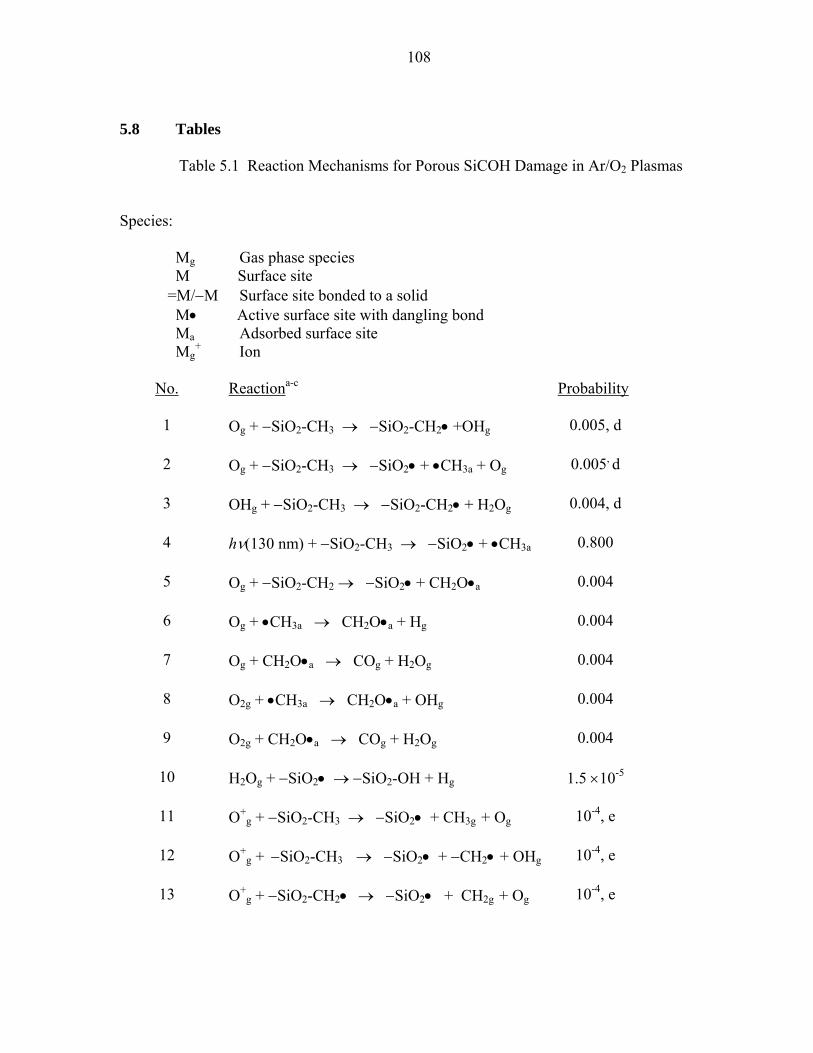
108
5.8 Tables
Table 5.1 Reaction Mechanisms for Porous SiCOH Damage in Ar/O2 Plasmas
Species:
Mg Gas phase species M Surface site =M/−M Surface site bonded to a solid M• Active surface site with dangling bond Ma Adsorbed surface site Mg
+ Ion
No. Reactiona-c Probability
1 Og + −SiO2-CH3 → −SiO2-CH2• +OHg 0.005, d
2 Og + −SiO2-CH3 → −SiO2• + •CH3a + Og 0.005, d
3 OHg + −SiO2-CH3 → −SiO2-CH2• + H2Og 0.004, d
4 hν(130 nm) + −SiO2-CH3 → −SiO2• + •CH3a 0.800
5 Og + −SiO2-CH2 → −SiO2• + CH2O•a 0.004
6 Og + •CH3a → CH2O•a + Hg 0.004
7 Og + CH2O•a → COg + H2Og 0.004
8 O2g + •CH3a → CH2O•a + OHg 0.004
9 O2g + CH2O•a → COg + H2Og 0.004
10 H2Og + −SiO2• → −SiO2-OH + Hg 1.5 ×10⁻⁵
11 O+g + −SiO2-CH3 → −SiO2• + CH3g + Og 10-4, e
12 O+g + −SiO2-CH3 → −SiO2• + −CH2• + OHg 10-4, e
13 O+g + −SiO2-CH2• → −SiO2• + CH2g + Og 10-4, e

109
Table 5.1 (Continued)
14 O+g + −SiO2-CH2• → −SiO2• + −CH•• + OHg 10-4, e
15 O2+
g + −SiO2-CH3 → −SiO2• + CH3g + O2g 10-4, e
16 O2+
g + −SiO2-CH3 → −SiO2• + CH2O•a + OHg 10-4, e
17 O2+
g + −SiO2-CH2• → −SiO2• + CH2g + O2g 10-4, e
18 O2+
g + −SiO2-CH2• → −SiO2• + CH2O•a + Og 10-4, e
19 O+g + •CH3a → CH3g + Og 10-4, e
20 O2+
g + •CH3a → CH3g + O2g 10-4, e
a. Unless specified, all ions neutralize on surfaces, returning as their neutral counterparts.
b. Gas phase species have units of flux (cm−2 s−1). Surface species have units of fractional
coverage.
c. In reactions with no chemical change, the gas species are reflected off the surface. These
reactions are not shown.
d. Er=3.5 eV, Et=0.18 eV, probability is at Er.
e. Er=100 eV, Et=10 eV, probability is at Er.

110
Table 5.2 Reaction Mechanisms for Porous SiCOH Damage in He/H2 Plasmas Species:
Mg Gas phase species M Surface site =M/−M Surface site bonded to a solid M• Active surface site with dangling bonds Ma Adsorbed surface site Mg
+ Ion
Reaction Reactiona-c Probability
1 hν (≈58 nm) + −SiO2-CH3 → −SiO2• + •CH3a 0.9
2 He+g + −SiO2-CH3 → −SiO2-CH2• + Hg + Heg 0.4, d
2 He+g + −SiO2-CH2• → −SiO2-CH•• + Hg + Heg 0.4, d
3 He+g + −SiO2-CH•• → −SiO2-C••• + Hg + Heg 0.4, d
4 He+g+ −SiO2• → =SiO•• + −O• + Heg 0.4, d
5 He+g+ =SiO•• → −Si••• + −O• + Heg 0.4, d
6 Hg + −SiO2-CH3 → −SiO2• + CH4g 10-5, e
7 Hg + −SiO2-C••• → −SiO2-CH•• 10-5
8 Hg + −SiO2-CH•• → −SiO2-CH2• 10-5, e
9 Hg + −SiO2-CH2• → −SiO2-CH3 10-5, e
10 Hg + −SiOn• → −SiOn-H 0.1
11 Hg + −Si••• → −Si-H•• 0.01
12 Hg + −Si-Hx• → −Si-Hx+1 0.001
13 Hg + •CH3a → CH4g 0.03, f
14 Hg + −O• → −OH 0.01
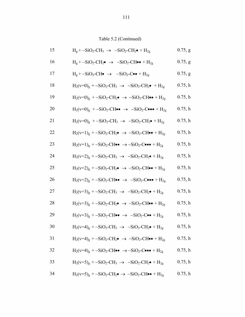
111
Table 5.2 (Continued)
15 Hg + −SiO2-CH3 → −SiO2-CH2• + H2g 0.75, g
16 Hg + −SiO2-CH2• → −SiO2-CH•• + H2g 0.75, g
17 Hg + −SiO2-CH• → −SiO2-C•• + H2g 0.75, g
18 H2(v=0)g + −SiO2-CH3 → −SiO2-CH2• + H2g 0.75, h
19 H2(v=0)g + −SiO2-CH2• → −SiO2-CH•• + H2g 0.75, h
20 H2(v=0)g + −SiO2-CH•• → −SiO2-C••• + H2g 0.75, h
21 H2(v=0)g + −SiO2-CH3 → −SiO2-CH2• + H2g 0.75, h
22 H2(v=1)g + −SiO2-CH2• → −SiO2-CH•• + H2g 0.75, h
23 H2(v=1)g + −SiO2-CH•• → −SiO2-C••• + H2g 0.75, h
24 H2(v=2)g + −SiO2-CH3 → −SiO2-CH2• + H2g 0.75, h
25 H2(v=2)g + −SiO2-CH2• → −SiO2-CH•• + H2g 0.75, h
26 H2(v=2)g + −SiO2-CH•• → −SiO2-C••• + H2g 0.75, h
27 H2(v=3)g + −SiO2-CH3 → −SiO2-CH2• + H2g 0.75, h
28 H2(v=3)g + −SiO2-CH2• → −SiO2-CH•• + H2g 0.75, h
29 H2(v=3)g + −SiO2-CH•• → −SiO2-C•• + H2g 0.75, h
30 H2(v=4)g + −SiO2-CH3 → −SiO2-CH2• + H2g 0.75, h
31 H2(v=4)g + −SiO2-CH2• → −SiO2-CH•• + H2g 0.75, h
32 H2(v=4)g + −SiO2-CH•• → −SiO2-C••• + H2g 0.75, h
33 H2(v=5)g + −SiO2-CH3 → −SiO2-CH2• + H2g 0.75, h
34 H2(v=5)g + −SiO2-CH2• → −SiO2-CH•• + H2g 0.75, h

112
Table 5.2 (continued)
35 H2(v=5)g + −SiO2-CH• → −SiO2-C••• + H2g 0.75, h
a. Unless specified, all ions neutralize on surfaces, returning as their neutral counterparts.
b. Gas phase species have units of flux (cm−2 s−1). Surface species have units of fractional
coverage.
c. In reactions with no chemical change, the gas species are reflected off the surface. These
reactions are not shown.
d. Er=100.0 eV, Et=10.0 eV, probability is at Er.
e. Er=3.5 eV, Et=0.5 eV, probability is at Er.
f. Er=3.5 eV, Et=0.03 eV, probability is at Er.
g. Er=3.5 eV, Et=1.0 eV, probability is at Er.
h. Er=3.5 eV, Et=0.3 eV, probability is at Er.
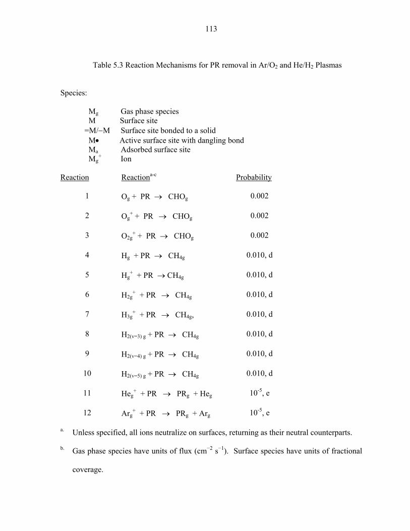
113
Table 5.3 Reaction Mechanisms for PR removal in Ar/O2 and He/H2 Plasmas
Species:
Mg Gas phase species M Surface site =M/−M Surface site bonded to a solid M• Active surface site with dangling bond Ma Adsorbed surface site Mg
+ Ion
Reaction Reactiona-c Probability
1 Og + PR → CHOg 0.002
2 Og+ + PR → CHOg 0.002
3 O2g+ + PR → CHOg 0.002
4 Hg + PR → CH4g 0.010, d
5 Hg+ + PR → CH4g 0.010, d
6 H2g+ + PR → CH4g 0.010, d
7 H3g+ + PR → CH4g, 0.010, d
8 H2(v=3) g + PR → CH4g 0.010, d
9 H2(v=4) g + PR → CH4g 0.010, d
10 H2(v=5) g + PR → CH4g 0.010, d
11 Heg+ + PR → PRg + Heg 10-5, e
12 Arg+ + PR → PRg + Arg 10-5, e
a. Unless specified, all ions neutralize on surfaces, returning as their neutral counterparts.
b. Gas phase species have units of flux (cm−2 s−1). Surface species have units of fractional
coverage.

114
c. In reactions with no chemical change, the gas species are reflected off the surface. These
reactions are not shown.
d. Er=100 eV, Et=1.4 eV, probability is at Er.
e. Er=100 eV, Et=10 eV, probability is at Er.
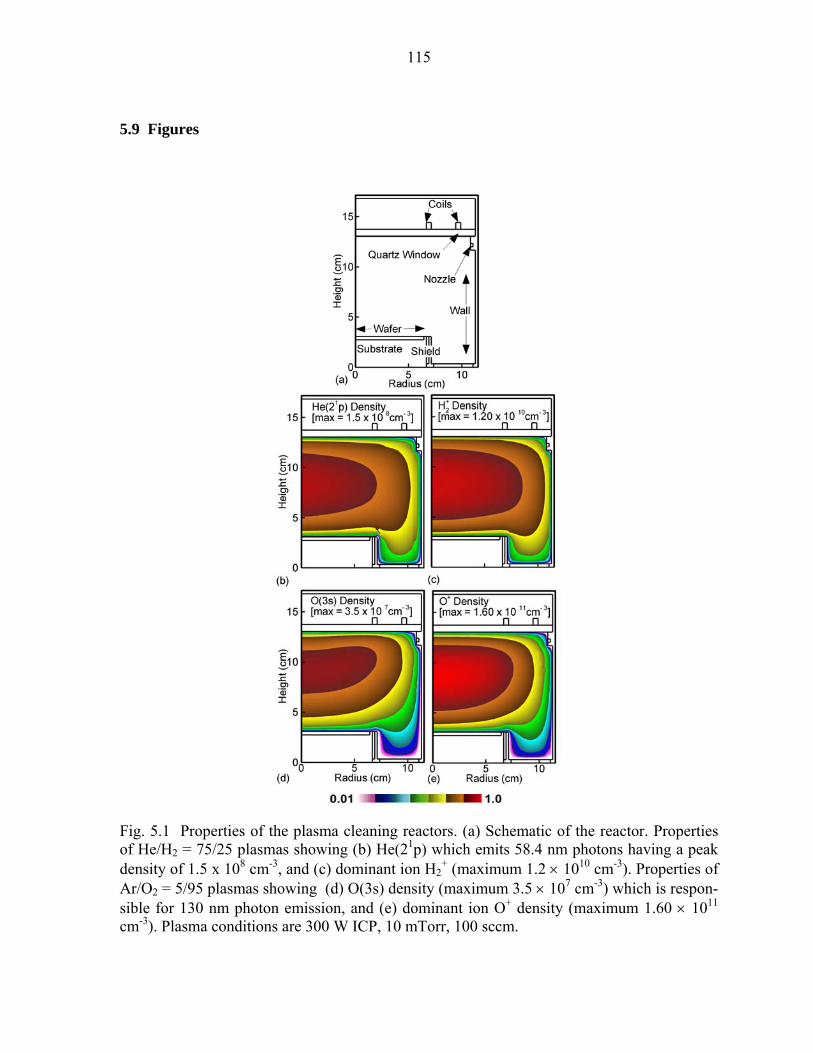
115
5.9 Figures
Fig. 5.1 Properties of the plasma cleaning reactors. (a) Schematic of the reactor. Properties of He/H2 = 75/25 plasmas showing (b) He(21p) which emits 58.4 nm photons having a peak density of 1.5 x 108 cm-3, and (c) dominant ion H2
+ (maximum 1.2 × 1010 cm-3). Properties of Ar/O2 = 5/95 plasmas showing (d) O(3s) density (maximum 3.5 × 107 cm-3) which is respon-sible for 130 nm photon emission, and (e) dominant ion O+ density (maximum 1.60 × 1011 cm-3). Plasma conditions are 300 W ICP, 10 mTorr, 100 sccm.

116
Fig. 5.2 Fluxes to the wafer. (a) Ion, photon, and neutral fluxes for He/H2 plasmas as a function of radius. (b) Ion, photon, and neutral fluxes for Ar/O2 plasmas. The scaling for fluxes is indicated in the figure. (He/H2=75/25, 300 W ICP, 10 mTorr, 100 sccm; Ar/O2=05/95, 300 W ICP, 10 mTorr, 100 sccm).

117
Fig. 5.3 Optimization of hot H (energy > 0.5 eV) fluxes to the wafer by varying pressure (He/H2=75/25, 300 W ICP, 100 sccm). (a) Energy and angular distribution of H atoms for pressures of 10 mTorr, 30 mTorr, and 80 mTorr. (b) Total H flux, and hot H flux (energy > 0.5 eV and energy > 1.0 eV) as a function of pressure. The scaling for fluxes is indicated in the figure.
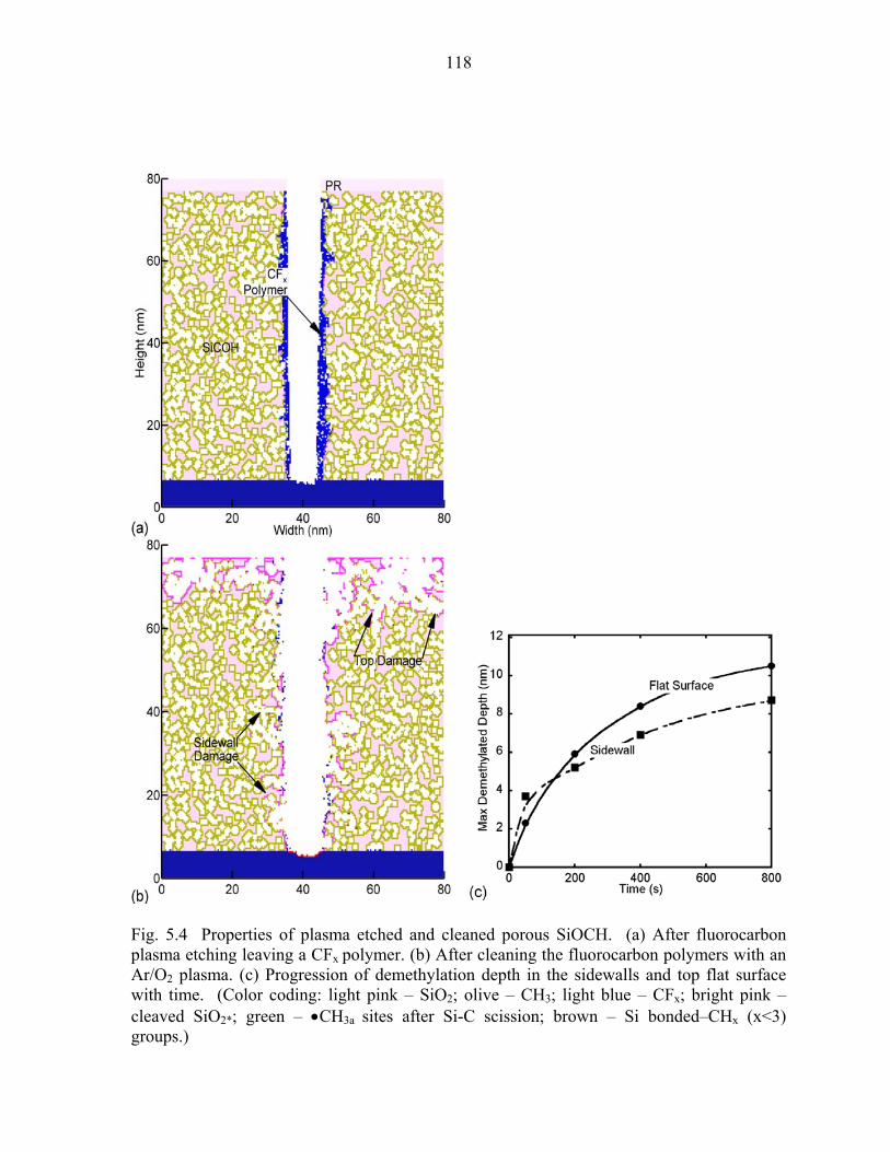
118
Fig. 5.4 Properties of plasma etched and cleaned porous SiOCH. (a) After fluorocarbon plasma etching leaving a CFx polymer. (b) After cleaning the fluorocarbon polymers with an Ar/O2 plasma. (c) Progression of demethylation depth in the sidewalls and top flat surface with time. (Color coding: light pink – SiO2; olive – CH3; light blue – CFx; bright pink – cleaved SiO2*; green – •CH3a sites after Si-C scission; brown – Si bonded–CHx (x<3) groups.)

119
Fig. 5.5 Photon flux as a function of power and demethylation depth as a function of photon flux. VUV photon flux in: (a) He/H2, and (b) Ar/O2 plasmas as a function of ICP power. (c) Damage depth in SiOCH as a function of photon flux. The damage depth is initially linear with photon flux but later the rate of damage decreases as most of the Si-CH3 sites are within the absorption depth of the photons have undergone scission.
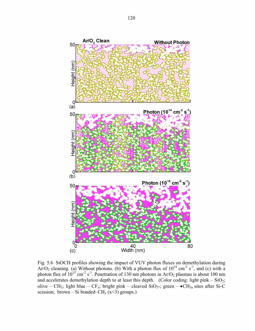
120
Fig. 5.6 SiOCH profiles showing the impact of VUV photon fluxes on demethylation during Ar/O2 cleaning. (a) Without photons. (b) With a photon flux of 1014 cm-2 s-1, and (c) with a photon flux of 1015 cm-2 s-1. Penetration of 130 nm photons in Ar/O2 plasmas is about 100 nm and accelerates demethylation depth to at least this depth. (Color coding: light pink – SiO2; olive – CH3; light blue – CFx; bright pink – cleaved SiO2*; green – •CH3a sites after Si-C scission; brown – Si bonded–CHx (x<3) groups.)

121
Fig. 5.7 SiOCH profiles showing the impact of VUV photon fluxes on demethylation during He/H2 cleaning. (a) Without photons. (b) With a photon flux of 1014 cm-2 s-1, and (c) with a photon flux of 1015 cm-2 s-1. Penetration of 58 nm photons in He/H2 plasmas is about 20-30 nm and accelerates demethylation depth to at least this depth. (Color coding: light pink – SiO2; olive – CH3; light blue – CFx; bright pink – cleaved SiO2*; green – •CH3a sites after Si-C scission; brown – Si bonded–CHx (x<3) groups.)
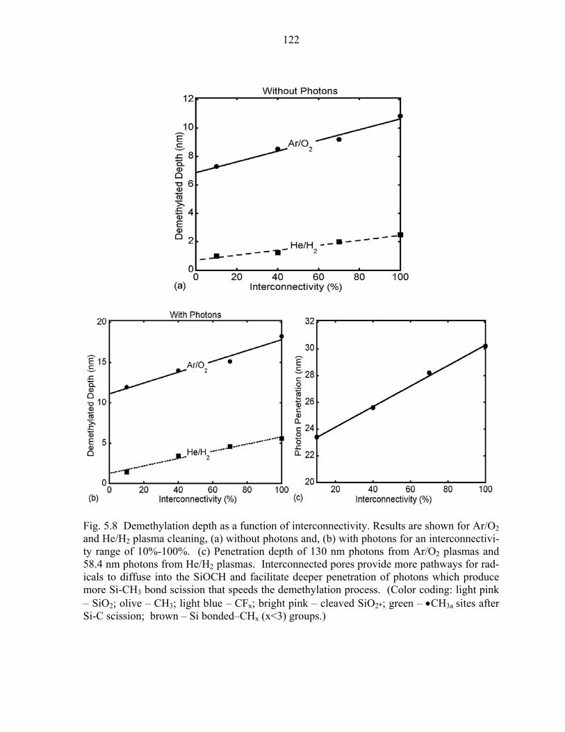
122
Fig. 5.8 Demethylation depth as a function of interconnectivity. Results are shown for Ar/O2 and He/H2 plasma cleaning, (a) without photons and, (b) with photons for an interconnectivi-ty range of 10%-100%. (c) Penetration depth of 130 nm photons from Ar/O2 plasmas and 58.4 nm photons from He/H2 plasmas. Interconnected pores provide more pathways for rad-icals to diffuse into the SiOCH and facilitate deeper penetration of photons which produce more Si-CH3 bond scission that speeds the demethylation process. (Color coding: light pink – SiO2; olive – CH3; light blue – CFx; bright pink – cleaved SiO2*; green – •CH3a sites after Si-C scission; brown – Si bonded–CHx (x<3) groups.)

123
Fig. 5.9 Profiles showing the effects of interconnectivity on demethylation during Ar/O2 cleaning. Profiles are shown for interconnectivities, (a) 10%, (b) 40%, and (c) 100%. De-methylated depth increases almost linearly with interconnectivity. (Color coding: light pink – SiO2; olive – CH3; light blue – CFx; bright pink – cleaved SiO2*; green – •CH3a sites after Si-C scission; brown – Si bonded–CHx (x<3) groups.)

124
Fig. 5.10 Profiles showing interconnectivity effects on demethylation during He/H2 cleaning. Profiles are shown for interconnectivities, (a) 10%, (b) 40%, and (c) 100%. Damage depth increases almost linearly with interconnectivity as for Ar/O2 plasma cleaning. (Color coding: light pink – SiO2; olive – CH3; light blue – CFx; bright pink – cleaved SiO2*; green – •CH3a sites after Si-C scission; brown – Si bonded–CHx (x<3) groups.)
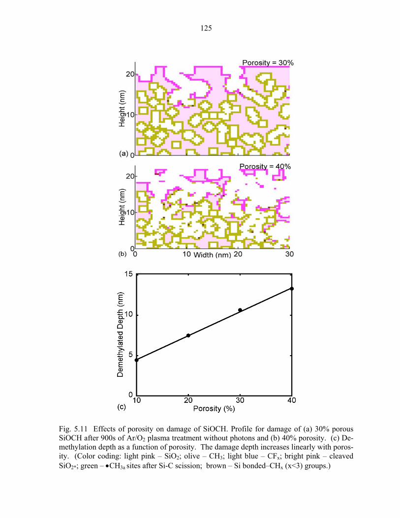
125
Fig. 5.11 Effects of porosity on damage of SiOCH. Profile for damage of (a) 30% porous SiOCH after 900s of Ar/O2 plasma treatment without photons and (b) 40% porosity. (c) De-methylation depth as a function of porosity. The damage depth increases linearly with poros-ity. (Color coding: light pink – SiO2; olive – CH3; light blue – CFx; bright pink – cleaved SiO2*; green – •CH3a sites after Si-C scission; brown – Si bonded–CHx (x<3) groups.)

126
Fig. 5.12 SiOCH treated with different fluxes of VUV photons for the same fluence. Ar/O2 plasma clean with a 5×1014 cm-2s-1 photon flux treated for 1600s, and (b) 1015 cm-2 s-1 flux treated for 800s. (c) He/H2 plasma clean with a 5×1014 cm-2s-1 photon flux treated for 1600s and (b) 1015 cm-2 s-1 flux treated for 800s. For a constant fluence, the amount of Si-C bond scission is essentially same but for longer treatment times, there is more opportunity for radi-cal fluxes to diffuse into the SiOCH and so cause more damage. (Color coding: light pink – SiO2; olive – CH3; light blue – CFx; bright pink – cleaved SiO2*; green – •CH3a sites after Si-C scission; brown – Si bonded –CHx (x<3) groups.)
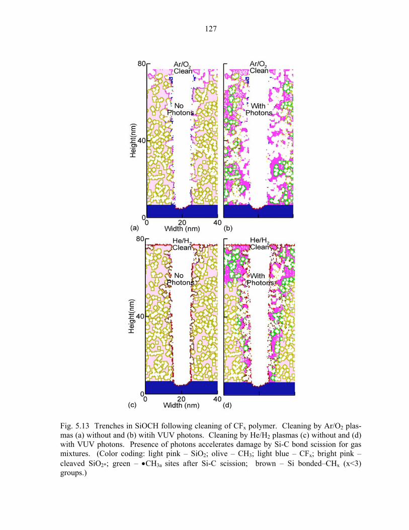
127
Fig. 5.13 Trenches in SiOCH following cleaning of CFx polymer. Cleaning by Ar/O2 plas-mas (a) without and (b) witih VUV photons. Cleaning by He/H2 plasmas (c) without and (d) with VUV photons. Presence of photons accelerates damage by Si-C bond scission for gas mixtures. (Color coding: light pink – SiO2; olive – CH3; light blue – CFx; bright pink – cleaved SiO2*; green – •CH3a sites after Si-C scission; brown – Si bonded–CHx (x<3) groups.)
128
5.10 References
1. M. R. Baklanov, K. P. Mogilnikov, and Q. T. Le, Microelectron. Eng. 83 2287 (2006).
K. Maex, M. Baklanov, D. Shamiryan, F. Iacopi, S. H. Brongersma, K. Maex, and Z. S.
Yanovitskaya, J. Appl. Phys. 93, 8793 (2003).
2. G. Mannaert, M. R. Baklanov, Q. T. Le, Y. Travaly, W. Boullart, S. Vanhaelemeersch,
and A. M. Jonas J. Vac. Sci. Technol. B 23, 2198 (2005).
3. H. Seo, S. B. Kim, J. Song, Y. Kim, H. Soh, Y. C. Kim, and H. Jeon, J. Vac. Sci. Tech-
nol. B 20, 1548 (2002).
4. K. Sakuma, K. Machida, K. Kamoshida, Y. Sato, K. Imai, and E. Arai, J. Vac. Sci.
Technol. B 13, 902 (1995).
5. M. A. Hartney, D. W. Hess, and D. S. Soane, J. Vac. Sci. Technol. B 7, 1 (1989).
6. E. Kondoh, T. Asano, A. Nakashima, and M. Komatu, J. Vac. Sci. Technol. B 18, 1276
(2000).
7. M. A. Goldman, D. B. Graves, G. A. Antonelli, S. P. Behera, and J. A. Kelber, J. Appl.
Phys. 106, 013311 (2009).
8. H. Shi, J. Bao, R. S. Smith, H. Huang, J. Liu, P. S. Ho, M. L. McSwiney, M. Moinpour,
and G. M. Kloster, Appl. Phys. Lett. 93, 192909 (2008).
9. J. Proost, E. Kondoh, G. Vereecke, M. Heyns, and K. Maex, J. Vac. Sci. Technol. B 16,
2091 (1998).
10. J. Proost, M. Baklanov, K. Maex, and L. Delaey, J. Vac. Sci. Technol. B 18, 303 (2000).
11. D. Shamiryan, M. R. Baklanov, S. Vanhaelemeersch, and K. Maex, J. Vac. Sci. Technol.
B 20, 1923 (2002).
12. M. Urbanowicz, M. R. Baklanov, J. Heijlen, Y. Travaly, and A. Cockburn, Electrochem.
129
Solid-State Lett. 10, G76 (2007).
13. A. M. Urbanowicz, D. Shamiryan, A. Zaka, P. Verdonck, S. De Gendt and M. R. Bak-
lanov, J. Electrochem. Soc. 157, H565 (2010).
14. F. N. Dultsev, A. M. Urbanowicz, and M. R. Baklanov, Mater. Res. Soc. Symp. Proc.
Vol. 1079 (Materials Research Society 1079-N07-03, 2008).
15. K. Vanstreels, and A. M. Urbanowicz, J. Vac. Sci. Technol. B, 28, 173 (2010).
16. M. J. Kushner, J. Phys. D 42, 194013 (2009).
17. K. Rajaraman1 and M. J. Kushner J. Phys. D: Appl. Phys. 37, 1780 (2004).
18. J. Shoeb and M. J. Kushner, “Damage by Radicals and Photons during Plasma Cleaning
of Porous Low-k SiOCH Part II: Water Uptake and Change in Dielectric Constant”.
19. A. Agarwal and M. J. Kushner, J. Vac. Sci. Technol. A 27, 37 (2009).
20. A. Sankaran and M. J. Kushner, J. Vac. Sci. Technol. A 22, 1242 (2004).
21. F. Ossler, J. Larsson, and M. Alden, Chem. Phys. Lett. 250, 287 (1996).
22. J. Lee and D. B. Graves, J. Phys. D 43, 425201 (2010).
23. J. R. Woodworth, M. E. Riley, V. A. Amatucci, T. W. Hamilton, and B. P. Aragon, J.
Vac. Sci. Technol. A 19, 45 (2001).
24. B. Jinnai, S. Fukuda, H. Ohtake, and S. Samukawa, J. Appl. Phys. 107, 043302 (2010).
25. M. Chaudhari, J. Du, S. Behera, S. Manandhar, S. Gaddam, and J. Kelber, Appl. Phys.
Lett. 94, 204102 (2009).
26. O. V. Braginsky, A. S. Kovalev, D. V. Lopaev, E. M. Malykhin, Yu. A. Mankelevich, T.
V. Rakhimova, A. T. Rakhimov, A. N. Vasilieva, S. M. Zyryanov, and M. R. Baklanov,
J. Appl. Phys. 108, 073303 (2010).

130
27. M.F.A.M. Van Hest, A. Klaver, D.C. Schram, and M.C.M. Van De Sanden, Thin Solid
Films 449 40 (2004).
28. M. A. Worsley, S. F. Bent, S. M. Gates, N. C. M. Fuller, W. Volksen, M. Steen and T.
Dalton, J. Vac. Sci. Technol. B 23, 395 (2005).
29. K. Singh, A. A. Kumbhar, and R. O. Dusane, Materials Letters 60 1579 (2006).
30. J. Pelletier and M. J. Cooke, J. Vac. Sci. Technol. B 7, 59 (1989).
31. K. Hassouni, T. A. Grotjohn, and A. Gicquel, J. Appl. Phys. 86 134 (1999).
32. G. D. Billing and E. R. Fisher, J. Chem. Phys. 18, 225, (1976).
33. T. Kikkawa, S. Kuroki, S. Sakamoto, K. Kohmura, H. Tanaka, and N. Hata, Journal of
The Electrochemical Society, 152(7), G560 (2005).
34. M. Wang and M. J. Kushner, J. Appl. Phys. 107, 023309 (2010).

131
6. NUMERICAL INVESTIGATION OF LOW-k DEGRADATION BY HUMID AIR
6.1 Introduction
Low dielectric constant (low-k) materials are now used for the inter-layer dielectric
in the fabrication of microelectronics devices to lower the RC time constant for signal prop-
agation.[1] One such low-k material is porous SiO2 with hydrophobic methyl groups
(−CH3) lining the pores – SiOCH. Such pristine low-k materials are essentially hydrophobic
because of the presence of these hydrophobic −CH3 groups on the pore walls which prevent
SiO2 from adsorbing water from humid air. As a result SiOCH usually does not contain
more than a few percent of physisorbed water in its volume even when the humidity is
high.[2] Even if this water does get inside the SiOCH by transport though the interconnected
network,[2] this physisorbed water can be driven out with mild heating (200-300 C) without
harming the integrity of the SiOCH.[1] If the hydrophobic –CH3 groups are etched creating
free radical sites, −SiO2•, (or chemically reactive sites), reactions can occur with water va-
por through chemisorption forming, for example, −SiO2-OH. These sites cause the SiOCH
to lose its hydrophobic nature by more easily enabling hydrogen bonding with additional
water vapor. With the high dielectric constant of water (≈80), such reactions potentially in-
crease the k value of SiOCH. As such, preservation of –CH3 groups on pore walls is desired
for maintaining the low-k integrity of SiOCH.
The CFx polymers which are deposited during the etching of SiOCH in fluorocarbon
plasmas must be removed as these compounds may cause compatibility issues in subsequent
processing steps.[3] Such polymers can also introduce some hydrophilic properties to Si-
OCH as they are not as hydrophobic as −CHx groups.[2] The removal of the CFx layer

132
would ideally be performed using an oxygen containing plasma due to the efficiency of oxi-
dation of the polymer by oxygen radicals.[4-6] However, O2 plasma cleaning can also re-
move the hydrophobic methyl groups from SiOCH that will, as described above, make the
SiOCH less hydrophobic and possible lead to an increase in its k-value. SiOCH is relatively
stable when H2 plasmas are used for cleaning with minimal removal of –CH3 groups.[7]
When correlating SiOCH etch rates with damaged produced by plasma cleaning, He/H2
plasma cleaning has been reported to result in one third etch the etch rate produced by Ar/O2
plasma etching plasmas under similar conditions.[8] Given that He/H2 plasma cleaning is
relatively benign to the underlying SiOCH, these systems are being investigated for photo-
resist (PR) mask removal.[9]
An unavoidable outcome of plasma cleaning of SiOCH is illumination with UV and
VUV photons. For example, plasmas containing O2 produce photon fluxes in the 130-145
nm range which have penetration distances >100 nm. In He/H2 plasmas, the resonance radi-
ation for He at 58.4 nm penetrates only ≈20 nm.[10] These UV/VUV photons can produce
Si-C bond scission in −SiO2-CH3 which can accelerate the –CH3 removal process.[11,12]
Since the –CH3 removal process by O atoms is exothermic, demethylation is enhanced by
VUV fluxes, but is not a prerequisite for demethylation. However, the deeper penetration
depth into SiOCH of photons from Ar/O2 plasmas magnifies the influence they have. On
the other hand, demethylation by the intrinsically less reactive He/H2 plasmas is greatly en-
hanced by the Si-C bond scission produced by VUV photons. However, the shorter penetra-
tion depth of VUV fluxes produced in He/H2 plasmas limits the range of this enhancement.
Exposure of SiOCH to humid air results in water uptake due to reaction of H2O with
free radical sites −SiO2• resulting from oxidation or bond-scission that removes −CH3. The

133
end result is formation of hydrophilic −SiO2-OH. That is, hydrophobic –CH3 group from
−SiO2-CH3 is replaced by hydrophilic –OH group. The presence of −SiO2-OH enables fur-
ther water uptake, creates –SiO2-OH(H2O) type compounds through hydrogen bonding.[13-
15] Given the high dielectric constant of water (≈80), loss of hydrophobic –CH3 groups af-
ter O2 plasma cleaning of SiOCH and incorporation of water from humid air can cause an
increase in the dielectric constant from 2.5 to 20 within 9 minutes.[1]
One of the strategies to reduce or eliminate the increase in dielectric constant result-
ing from water intake is to seal the pores. A number of different techniques have been de-
veloped for pore sealing, including densification of the surface with a plasma treatment and
formation of a sealing layer of Si-N and C-N compounds with a NH3 plasma treatment. Pre-
treatment with He plasmas is thought to create active surface sites which localize and accel-
erate the chemical reactions responsible for pore sealing.[16-18] The processes whereby
subsequent NH3 plasma treatment completes the sealing are uncertain but at least two mech-
anisms have been proposed. The first proposes that NH3 plasma treatment catalyzes pore
collapse and so produces a dense non-porous layer at the surface.[19] The second proposes
that chemisorption of NHx radicals result in Si-N and C-N bonding which leads to bridging
of the opening of the pores.[16-18]
The He ions produced in He/H2 plasma cleaning also aids in preconditioning the sur-
face which improves pore sealing by subsequent treatment using NH3 containing plas-
mas.[16-18] The preconditioning promotes formation of Si-N and C-N bonding which pro-
duces a 1-2 monolayer thick sealing layer. The protective layer helps prevent water mole-
cules from humid air from entering the porous network. Due to He/H2 plasmas being less
reactive with –CH3 groups and also able to precondition the SiOCH for subsequent pore

134
sealing in NH3 plasmas, He/H2 plasmas are attractive candidates for cleaning SiOCH and
helping to maintain its low-k nature.
In this chapter, we discuss reaction mechanisms and computationally investigate the
change in dielectric constant due to water uptake from humid air after polymer cleaning from
SiOCH with Ar/O2 and He/H2 plasmas. This study is a follow-on to a more general investi-
gation of damage mechanisms of SiOCH by plasma cleaning (including VUV photons) dis-
cussed in Chapter 5.[20] Change in the dielectric constant of the SiOCH k value was as-
sessed using the amount of water adsorbed with exposure to humid air after cleaning.
The reaction mechanism for damage of SiOCH in Ar/O2 and He/H2 is discussed in
Chapter 5, and so will be only briefly discussed in Sec. 6.2 along with mechanism for water
uptake and increase in dielectric constant. A comparison of low-k degradation (that is, in-
crease in dielectric constant of SiOCH) after Ar/O2 and He/H2 plasma cleaning is discussed
in Sec. 6.3 and preservation of low-k properties by pore sealing are discussed in Sec. 6.4.
Comparison of our results with experiments is in Sec. 6.5 and our concluding remarks are in
Sec. 6.6.
6.2 Surface Reaction Mechanisms
Reaction mechanisms were developed for plasmas sustained in He/H2 and Ar/O2 mix-
tures and their interactions with low-k porous SiOCH, and is discussed in detail in Chapter
5.[20] In this chapter, the update of H2O molecules coming from humid air was included and
an assessment of the change in low-k properties of the SiOCH made based on the amount of
water in the pores. As in Chapter 5, the Hybrid Plasma Equipment Model (HPEM) was em-

135
ployed to obtain the energy and angular distributions of fluxes of charged and neutral spe-
cies, and of photon fluxes, incident onto the surface.[21] These fluxes and the reaction
mechanism was implemented in the Monte Carlo Feature Profile Model (MCFPM) with
which the evolution of the SiOCH properties are predicted.[22] The MCFPM resolves the
porous material with approximately atomic resolution. The cell size in this work is square
with 0.4 nm × 0.4 nm dimensions, which is an effective radius of 0.2 nm. The creation of
pores in the MCFPM mesh is discussed in Ref. [23]. The internal surfaces of the pores in
SiO2 were lined with a single layer of −CH3 to approximate the structure of SiOCH as dis-
cussed in Ref. [24].
When SiOCH is processed in an O2 containing plasma, the –CH3 groups of the porous
low-k are etched as CO/CO2 from deeper sites below the surface which O atoms reach by dif-
fusion through the interconnected porous network.[8,25,26] Photons produced by the plas-
ma having wavelength of <145 nm and penetrating into the SiOCH can break the Si-C bond
and initiate a series of reactions starting with production of an adsorbed •CH3a radical which
is removed by further reaction with O and O2.[11,12] The dominant reactions for methyl
group removal or demethylation in O2 plasmas is described in Chapter 5 and is summarized
as [8,11,20, 25-27],
Og + −SiO2-CH3 → −SiO2-CH2• +OHg, p = 0.005 (6.1)
Og + −SiO2-CH3 → −SiO2• + •CH3a + Og, p = 0.005 (6.2)
OHg + −SiO2-CH3 → −SiO2-CH2• + H2Og, p = 0.004 (6.3)
hν(130 nm) + −SiO2-CH3 → −SiO2• + •CH3a, p = 0.800 (6.4)

136
Og + −SiO2-CH2• → −SiO2• + CH2O•a, p = 0.004 (6.5)
Og + •CH3a → CH2O•a + Hg, p = 0.005 (6.6)
Og + CH2O•a → COg + H2Og, p = 0.004 (6.7)
O2g + CH2O•a → CO2g + H2Og, p = 0.004 (6.8)
O2g + •CH3a → CH2O•a + OHg, p = 0.004 (6.9)
O2g + CH2O•a → CO2g + H2Og, p = 0.004 (6.10)
H2Og + −SiO2• → −SiO2-OH + Hg. p = 1.5 × 10⁻⁵ (6.11)
Subscript g denotes a gas phase species, subscript a denotes an adsorbed species, the symbols
• represent a dangling bond or free radical site, and – (or =) represents bonding to the solid.
Note that there is a chain reaction where H abstraction by O or OH from −SiO2-CH3 produc-
es OH or H2O which can further react in the demethylation process.
He/H2 plasmas remove −CH3 groups from SiOCH at a slower rate primarily because
the reactions for −CH3 removal in He/H2 plasmas are either endothermic or proceed at a
slower rate than in Ar/O2 plasmas, and the reaction products are themselves less reactive. As
a result, photons from He/H2 plasmas which produce Si-C bond cleavage to separate –CH3
from Si can greatly accelerate the demethylation by enabling the •CH3a to be removed by H
atoms as CH4.[16,17, 27] After –CH3 removal from −SiO2-CH3, H atoms can passivate the
free radical site −SiO2• forming −SiO2-H where Si is bonded to H with a Si-H bond. Howev-
er, He+ can break Si-O bonding in −SiO2• and generate free radical site −SiO••, and a suc-
cessive strike can produce −Si•••. H can passivate −Si••• as −Si-Hn (n = 1-3). Such com-
pounds with Si-H bonds are hydrophobic in nature and can block water uptake.[28] The

137
analogous process in Ar/O2 plasmas produce hydrophyllic −SiO2-OH sites. The interaction
between He/H2 plasmas and SiCOH is discussed in Part I and is summarized as
[8,11,16,17,28],
hν (≈58 nm) + −SiO2-CH3 → −SiO2• + •CH3a, p = 0.9 (6.12)
He+g + −SiO2-CHn → −SiO2-CHn-1• + Hg + Heg, p = 0.6 (6.13)
He+g+ −SiO2• → =SiO•• + −O• + Heg, p = 0.4 (6.14)
He+g+ =SiO•• → −Si••• + −O• + Heg, p = 0.4 (6.15)
Hg + −SiO2-CH3 → −SiO2• + CH4g , p = 10-5 (6.16)
Hg + −SiO2-CHx → −SiO2-CHx+1, p = 10-5 (6.17)
Hg + −SiOn• → −SiOn-H, p = 0.10 (6.18)
Hg + −Si••• → −Si-H••, p = 0.01 (6.19)
Hg + −Si-Hx• → −Si-Hx+1, p = 0.001 (6.20)
Hg + •CH3a → CH4g, p = 0.03 (6.21)
Hg + −SiO2-(CHn) → −SiO2-(CHn-1)• + H2g, p = 0.75 (6.22)
Hg + −O• → −OH. p = 0.01 (6.23)
After Ar/O2 or He/H2 plasma cleaning and upon exposure to humid air, free radical
(−SiO2•) or passivated (−SiO2-OH) sites formed after −CH3 removal can react with water.
Any remaining •CH3a generated by photon produced Si-C bond scission in −SiO2-CH3 can
also be etched by H2O to form CH4 and OH, which can then produce more demethylation.
The general sequence of events is that −SiO2• on the pore-walls react with H2O to form hy-

138
drophillic −SiO2-OH. Additional water uptake can occur by reaction of −SiO2-OH with H2O
to form hydrogen bonded −SiO2-OH-(H2O). The volume averaged uptake of H2O with its
dielectric constant of 80, results in an increase of the dielectric constant of the SiOCH and a
degradation of the low-k properties. These reactions are be summarized as [11, 13-15],
H2Og + •CH3a → CH4g + OHg, p = 1.2 × 10⁻⁴ (6.24)
H2Og + −SiO2• → −SiO2-OH + Hg, p = 1.5 × 10⁻⁴ (6.25)
H2Og + −SiO2-OH → −SiO2-OH-(H2O). p = 1.5 × 10⁻⁴ (6.26)
Computationally, water exposure was addressed in the following manner. Fluxes of H2O and
O2 commensurate with humid air were directed towards the surface of the SiOCH with tra-
jectories randomly chosen isotropically in angle and from a Maxwellian velocity distribution
for room temperature. Gas phase collisions were included but are unimportant for the size of
porosity we are addressing. The method of computation was otherwise identical to that for
low pressure processing.
During the He/H2 plasma cleaning step, active sites SiOCH are produced that assist in
pore sealing during a subsequent Ar/NH3 plasma treatment.[16-18] He+ and VUV photons
break Si-O bonds and remove H from −CH3 groups lining the pores to create the active sites.
The bond breaking and site activation reactions are summarized as [16-18, 24],
He+g+ =SiO2 → =SiO• + =O• + Heg, (6.27)

139
hν + =SiO2 → =SiO• + =O•, (6.28)
He+g + −SiOn(CHn) → −SiOn(CHn-1)• + Hg + Heg, (6.29)
hν + −SiOn(CHn) → −SiOn(CHn-1)• + Hg, (6.30)
Hg + −SiO2(CHn) → −SiO2(CHn-1)• + H2g. (6.31)
Following He/H2 plasma treatment, NHn (n = 1, 2) species created in Ar/NH3 plasmas are
chemisorbed at activated sites on SiOCH forming Si-N and C-N bonds.[16-18, 24] Chemical
reactions between NHx radicals and activated Si sites produce compounds such as Si-NHn
(n=1, 2), =Si-NH-Si= and SiNHx-NHy.[16-18, 24] In SiOCH, C-N bonding is also possible
forming =CHx-NHy compounds which are important in bridging and sealing the pore open-
ings.[16-18, 24] The model treats these chemisorbed species as precursors to further adsorp-
tion of NHx which form N-N bonds linking C or Si atoms from opposite pore walls. This N-
N bonding results in, for example, =Si(HN)-(NH)(CHn)Si= bridging compounds across
pores. Our reaction mechanisms for sealing SiOCH is discussed in detail in Ref. [24], and
are summarized as [16-18, 24],
•NHxg+ −SiOn• → −SiOn-NHx p = 0.8 (6.32)
•NHxg + −SiO2-CHn• → −SiO2-CHn-NHx p = 0.4 (6.33)
•NHxg + −SiOn-NHx• → −SiOn-NHx-NHy p = 0.9 (6.34)
•NHxg + −SiO2-CHn-NHx• → −SiO2-CHn-NHx-NHy. p = 0.9 (6.35)

140
Such a sealing layer can prevent H2O molecules from entering the porous network and so
reduce the degree of low-k degradation. Experimentally, it has been observed that after such
sealing, humid air exposure does not significantly increase the water volume percentage
compared to pristine SiOCH.[17] This results indicates that H2O molecules from humid air
do not react with –NHx compounds to remove the sealing layer. As such, the –NHx sealing
layer essentially blocks water uptake.
Prior to plasma exposure, pristine SiOCH contains < 2% of physisorbed H2O which
can be removed by moderate heating (≈200 C) without otherwise detrimentally affecting the
material.[1,2,17] As a result, in our model, there is no adsorbed water nor hydrophyllic
groups present in the porous volume before plasma treatment. Consequences of water up-
take is measured by the effective dielectric constant of SiOCH, k’, which accounts for the
volume fraction of the water and the porosity,[29]
)(2
)(2
AWP
WW
AWP
WA
WP
kkVVk
kkVVk
kk−−
−+= , (6.36)
( )( )SPPPS
SPPPSS kkVkk
kkVkkkk−−+−++
=' , (6.37)
where dielectric constants are kW for water (80), kA for air (1.0), kP for a pore and kS for non-
porous SiOCH (≈3.2). VP is the volume fraction of pores and VW is the volume fraction of
water. k’ as a function of water volume VW is shown in Fig. 1a for a porosity VP = 30%. An
increase in VW of even a few percent for a given porosity increases k’ by significant amounts,

141
in this case to a dielectric constant of 5 for VW = 6%, due to the large dielectric constant of
water.
The plasma conditions are the same as in Chapter 5. The inductively coupled plas-
mas treated a wafer 15 cm in diameter. The reactor was 26 cm in diameter with a wafer-to-
coil height of 10 cm. The gas mixture were Ar/O2 = 5/95 and and He/H2 = 75/25 at a pres-
sure of 10 mTorr, flow rate of 100 sccm and ICP power of 300 W applied at 10 MHz. An rf
bias at 10 MHz with amplitude of 20 V was used. The base case properties of the SiOCH are
a porosity of 30%, pore radius of 0.8 nm with standard deviation of 10% and interconnectivi-
ty of 100%. This result in a dielectric constant of k = 2.55.
The probabilities for surface site modification, –CH3 etching reactions and sealing
have been determined by extensive parameterization of the models to be qualitatively con-
sistent with experimental results available in the literature. The mechanism for demethyla-
tion is described in Part I and for sealing in Ref. [24 ]. Bounds of reaction probabilities are
set based on thermodynamic properties and change in enthalpy of reactions, and within those
bounds parameterization and comparison to experiments refine the mechanism. Although the
majority of these reactions have a dependence on substrate temperature, our mechanism as-
sumes a fixed substrate temperature of 27 C while including energy dependencies for gas
phase radicals. Some examples of works that guided the development of the reactions are
discussed in section 6.6 to validate our mechanisms and reaction probabilities.
6.3 Low-k Degradation: Ar/O2 and He/H2 Cleaning
We treated the pristine porous SiOCH of Fig. 6.2a separately with 800 s exposure to
Ar/O2 and He/H2 plasmas. The Ar/O2 plasma etched the –CH3 groups to ≈30 nm depth while

142
the maximum etching depth for He/H2 plasmas was ≈10 nm. After each clean, the SiOCH
was exposed to air exposure with 2% for 120 s. The profiles of the pristine SiOCH, after
plasma exposure and after humid air exposure are shown in Fig. 6.2. Water uptake and die-
lectric constant as a function of air exposure time are shown in Fig. 6.3. After 120 s of hu-
mid air exposure, the total VW is 9% after Ar/O2 plasma cleaning, and 2% after He/H2 plasma
cleaning.
After a critical amount of water adsorption, the increase in VW as a function of time
slows. This is due to the blocking of pore openings by −SiO2-OH-(H2O) compounds. The
VW is composed to two components, chemisorbed −SiO2-OH and hydrogen bonded H2O. In
−SiO2-OH, the –OH is chemically bonded to −SiO2 (bond strength 8.3 eV) and so is not re-
movable by heating without damaging the SiOCH.[1] On the other hand, physisorbed hy-
drogen bonded H2O can be driven out from the SiOCH with heating to 200-300 C without
damaging the substrate.[1] The water uptake after Ar/O2 plasma exposure is roughly half
chemisorbed and half physisorbed. After He/H2 plasma exposure, the majority is chemi-
sorbed. The higher volume of water addition after Ar/O2 treatment than He/H2 treatment is
because –CH3 groups are more lost in the first treatment compared to the second. The more
reactive nature of O2 plasmas is primarily responsible for such increase in –CH3 consumption
in Ar/O2 plasmas. Since –CH3 removal from −SiO2-CH3 is the precondition for water uptake
or −SiO2-OH formation, the amount of water adsorbed is directly related to the number of –
CH3 groups lost. As such, for more etching of –CH3 groups in Ar/O2 plasmas than He/H2
cleaning, Ar/O2 cleaned profile adsorbed more water than He/H2 cleaned profile.

143
With the increase in VW, the increase in dielectric constant following Ar/O2 plasma
cleaning is 2.5 to 5.5 for Ar/O2 clean and; and 2.5 to 3.5 for He/H2 plasma cleaning. The
proportion of this increase which is apportioned between chemisorbed −SiO2-OH and hydro-
gen bonded –H2O is shown in Fig. 6.3c. About 60% of the increase in the dielectric constant
(to 4.5) following Ar/O2 plasma exposure is attributable to chemisorption. The remaining in-
crease is due to hydrogen bonded –H2O, which is in principle reversible by heating. Of the
increase in k to 3.5 for He/H2 plasma cleans, the increase attributable to −SiO2-OH is to 3.25.
As such, the irreversible increase in k rise is only 0.25.
We deposited a ≈10 nm thick CFx polymer layer on the top surface of SiOCH using a
capacitively coupled plasma sustained in an Ar/C4F8/O2 = 80/15/5 mixture at 40 mTorr, as
shown in Fig. 6.1b and Fig. 6.4a. The conditions are the same as in Chapter 5 except at a
lower bias to prevent etching. The polymer layer was then removed with a 20 s short expo-
sure to either the Ar/O2 and or He/H2 plasmas. The short cleaning was long enough to clean
the polymer layer but not long enough to produce deep damage into the SiOCH by diffusion
of radicals to enable investigation of the surface layers. However, a flux of 1016 cm-2s-1 pho-
tons from the plasmas produces Si-C bond scission deeper into the SiOCH than plasma dam-
age produced by O or H radicals. Later, during lengthy humid air exposure, H2O molecules
can etch adsorbed •CH3a and passivate the −SiO2• free radical sites to form −SiO2-OH-(H2O)
as shown in Fig. 6.4, which increases the dielectric constant k. This is an example of where
photon penetration into the SiOCH, even in the absence of further reactions with radicals
from the plasma, can lead to low-k degradation by humid air exposure.
6.4 Low k Integrity by Pore Sealing
We investigated the consequences on water uptake of pore sealing using Ar/NH3
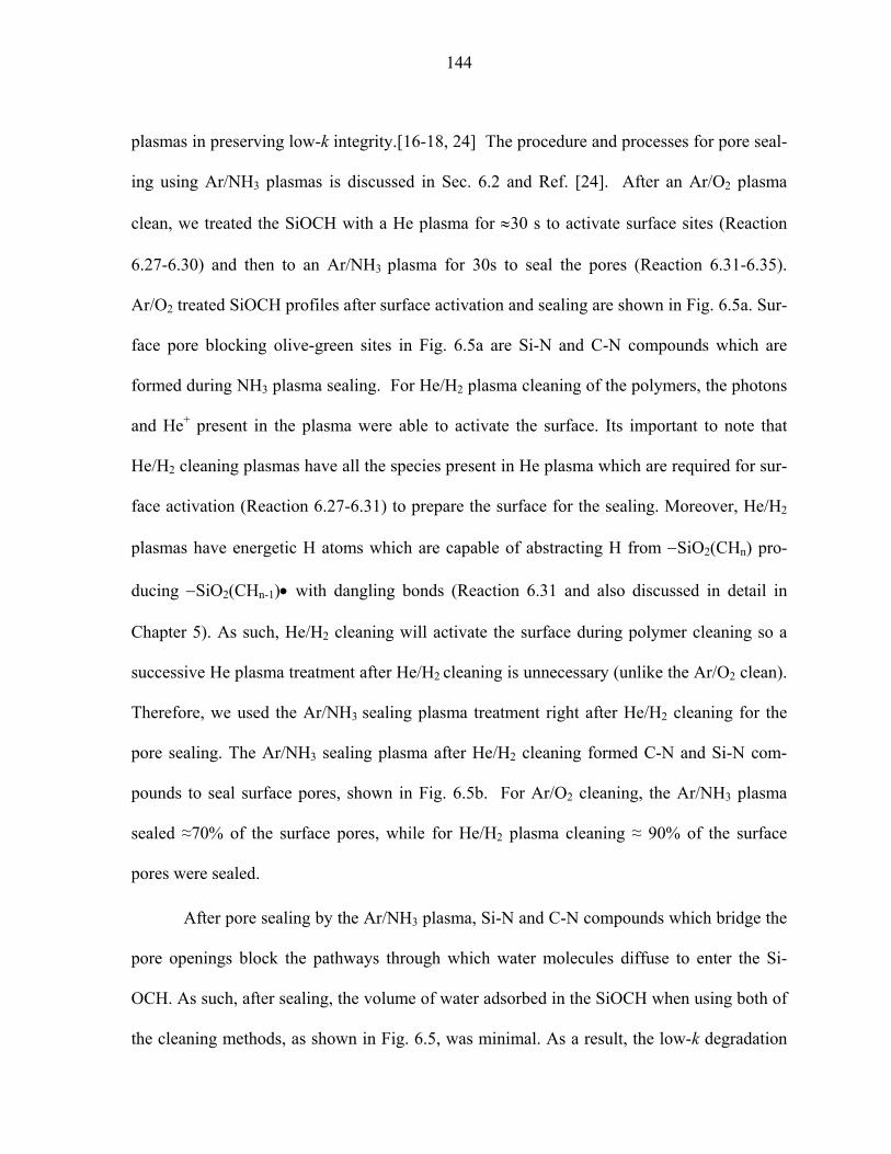
144
plasmas in preserving low-k integrity.[16-18, 24] The procedure and processes for pore seal-
ing using Ar/NH3 plasmas is discussed in Sec. 6.2 and Ref. [24]. After an Ar/O2 plasma
clean, we treated the SiOCH with a He plasma for ≈30 s to activate surface sites (Reaction
6.27-6.30) and then to an Ar/NH3 plasma for 30s to seal the pores (Reaction 6.31-6.35).
Ar/O2 treated SiOCH profiles after surface activation and sealing are shown in Fig. 6.5a. Sur-
face pore blocking olive-green sites in Fig. 6.5a are Si-N and C-N compounds which are
formed during NH3 plasma sealing. For He/H2 plasma cleaning of the polymers, the photons
and He+ present in the plasma were able to activate the surface. Its important to note that
He/H2 cleaning plasmas have all the species present in He plasma which are required for sur-
face activation (Reaction 6.27-6.31) to prepare the surface for the sealing. Moreover, He/H2
plasmas have energetic H atoms which are capable of abstracting H from −SiO2(CHn) pro-
ducing −SiO2(CHn-1)• with dangling bonds (Reaction 6.31 and also discussed in detail in
Chapter 5). As such, He/H2 cleaning will activate the surface during polymer cleaning so a
successive He plasma treatment after He/H2 cleaning is unnecessary (unlike the Ar/O2 clean).
Therefore, we used the Ar/NH3 sealing plasma treatment right after He/H2 cleaning for the
pore sealing. The Ar/NH3 sealing plasma after He/H2 cleaning formed C-N and Si-N com-
pounds to seal surface pores, shown in Fig. 6.5b. For Ar/O2 cleaning, the Ar/NH3 plasma
sealed ≈70% of the surface pores, while for He/H2 plasma cleaning ≈ 90% of the surface
pores were sealed.
After pore sealing by the Ar/NH3 plasma, Si-N and C-N compounds which bridge the
pore openings block the pathways through which water molecules diffuse to enter the Si-
OCH. As such, after sealing, the volume of water adsorbed in the SiOCH when using both of
the cleaning methods, as shown in Fig. 6.5, was minimal. As a result, the low-k degradation
145
after pore sealing was not significant, as shown in Fig. 6.6. The dielectric constant increased
from 2.5 to no more than 2.7 for both of the cleaning methods. The small increase in the k-
value resulted from incomplete sealing as the C-N and Si-N compounds are unable to bridge
all of the pore openings. Although the average pores size is 0.8 nm which is sealable by this
method, the statistical variation in pore size produces some pores having sizes that exceed the
sealable limit (about 1.1 nm). Also, during cleaning of polymers, the plasmas remove –CH3
groups from surface pore-entrance which enlarge the pore opening. As a result, there are a
few pores (in this case, about 30% for Ar/O2 clean and 10 % for He/H2 clean) which remain
unsealed which provide a pathway for H2O molecules to diffuse into the SiOCH.[24] This
effect will become more severed as the pore size increase and the fraction of pores that are
sealed decreases.
6.5 Comparison with Experimental Trends
The details of water uptake and increase in dielectric constant following humid air
exposure of plasma damaged SiOCH depend on the precise processing steps and properties
of the SiOCH (e.g., structure, porosity, interconnectivity). As a result, direct comparisons
with experiments are difficult. However, trends from the experiments are useful for qualita-
tive validation of the model. The general trends observed in experiments are that oxygen
containing plasma exposure of SiOCH followed by exposure to air can produce significant
increases in the k-value of the SiOCH. For example, Maex et al [1] exposed SiOCH to an
O2 plasma (300 mTorr, rf power 300 W, 300 °C) for 9 min long O2, and upon exposure to air
(humidity not specified), the k-value increased from 2 to 20.[1] This is a larger increase that
we predict, perhaps attributable to the elevated substrate temperature during plasma expo-
146
sure, 300 C, which may accelerate S-C bond scission by O atoms. Our computed trends of
more water update following Ar/O2 plasma exposure compared to He/H2 plasma exposure
correlate with experimental observations of damage in these systems. C depletion in Ar/O2
plasmas, which is the precursor to water adsorption, is 3-5 times more severe compared to
He/H2 plasmas.[8] Urbanowicz et al. found that He plasma pretreatment followed by a NH3
plasma was able to seal SiOCH pores to sufficient degree to block water uptake from humid
air − no low-k degradation was observed.[17] We also found after plasma sealing, for both
of the cleaning methods, the update of water was insignificant.
It has been reported, for a porous film of ≈30% porosity, adsorbed water volume per-
centage at first increases with increase in humidity for a humidity range of 0-15% and then
the rate of increase slows down when water volume is >10%. [29] We varied the humidity
for a range 0-7.5% and found the water volume first rises and then settle downs at ≈7.25 % as
shown in Fig. 6.7a. In literature, for a humidity of 0-10%, the dielectric constant of the low k
became > 4. [29] In our model, the k increased from 2.55 to 5.55 for the humidity range of 0-
7.5% (shown in Fig. 6.7b). As shown in the plots of Ref. 29, the relationships for water vol-
ume and k with increase in humidity is initially linear but later rise in water volume and k
slow down with increase in humidity which agrees with our observations that surface pore
blocking by −SiO2-OH-H2O compounds may eventually limit the amount of water uptake
and k degradation.
6.6 Concluding Remarks
Low-k degradation by humid air after Ar/O2 and He/H2 plasma cleaning of porous

147
SiOCH was investigated. Both of these cleans can remove hydrophobic –CH3 groups from
−SiO2-CH3 compounds exposing −SiO2 to H2O molecules coming from humid air that in-
creases k value by forming −SiO2-OH which later adsorbs another H2O molecule to form
−SiO2-OH-H2O. While hydrogen bonded H2O can be removed applying a moderate temper-
ature (200-300 C), the rise of k because of −SiO2-OH formation cannot be reversed because
Si-OH is tightly bonded. A cleaning such as He/H2 that etches –CH3 groups not so severely
compared to Ar/O2 plasmas will adsorb less amount of water and degrade the k value less
aggressively. If a short exposure of these cleaning plasmas is used, the reactive radicals do
not have enough time to etch –CH3 groups significantly but photons were able to cause Si-C
bond scission to create adsorbed –CH3a group which is separated from Si. As such, even af-
ter a short exposure, H2O of humid air will etch –CH3a as CH4. A sealing layer formation by
NH3 plasma exposure can form a thin layer of Si-NHx and C-NHx compounds that can pre-
vent water from entering the network. Such a sealing layer can preserve the low-k integrity
by blocking water uptake.

148
6.7 Figures
Fig. 6.1 Computed dielectric constant of the porous low-k as a function of water volume and polymer deposited low-k profile used for the investigation of low-k degradation. (a) Relation-ship between adsorbed water volume in the low-k and overall dielectric constant. (b) Porous SiCOH with deposited CFx polymer at the top to investigate the k degradation for such poly-mer cleaning in Ar/O2 and He/H2 plasmas. (Color coding: light pink – SiO2; brown – CH3; cyan – CFx polymers.)
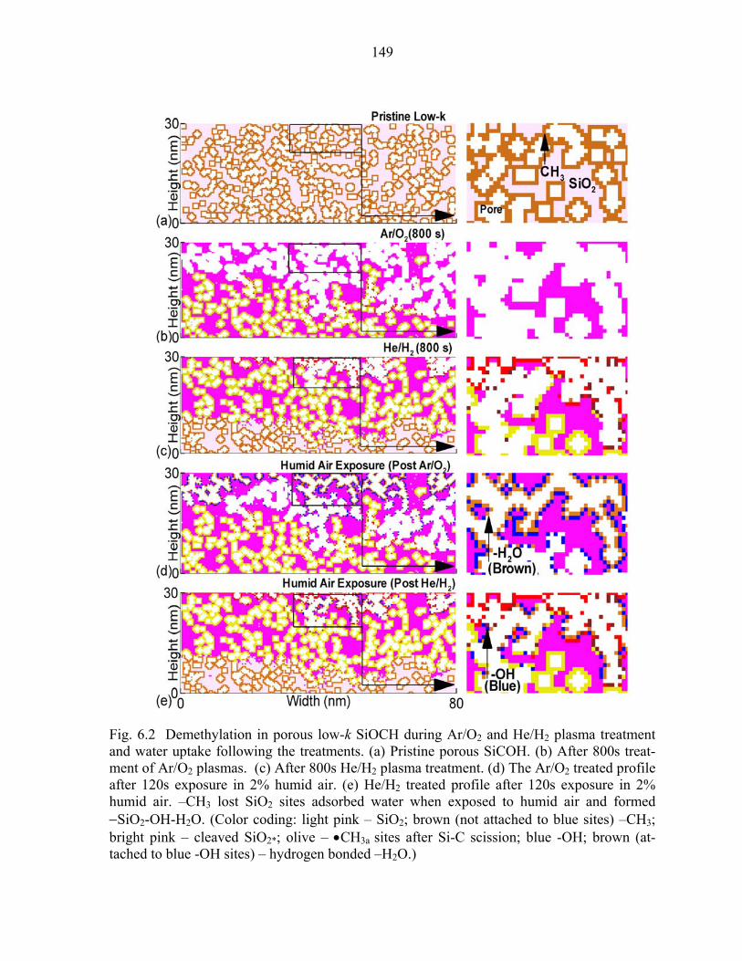
149
Fig. 6.2 Demethylation in porous low-k SiOCH during Ar/O2 and He/H2 plasma treatment and water uptake following the treatments. (a) Pristine porous SiCOH. (b) After 800s treat-ment of Ar/O2 plasmas. (c) After 800s He/H2 plasma treatment. (d) The Ar/O2 treated profile after 120s exposure in 2% humid air. (e) He/H2 treated profile after 120s exposure in 2% humid air. –CH3 lost SiO2 sites adsorbed water when exposed to humid air and formed −SiO2-OH-H2O. (Color coding: light pink – SiO2; brown (not attached to blue sites) –CH3; bright pink – cleaved SiO2*; olive – •CH3a sites after Si-C scission; blue -OH; brown (at-tached to blue -OH sites) – hydrogen bonded –H2O.)

150
Fig. 6.3 Classification of adsorbed water in the low-k based on if such water adsorption causes reversible or irreversible k increase. (a) Adsorbed water volume after cleaning as a function of time. (b) Increase in dielectric constant k as a function of time because of −SiO2-OH-H2O formation. Chemisorbed water is -OH while -H2O part is hydrogen bonded. Hydro-gen bonded H2O can be removed by applying ~300C but –OH removal requires >400C which will make porous low-k unstable. Increase in water volume and k slows down with time as −SiO2-OH-H2O compounds block the pore openings.
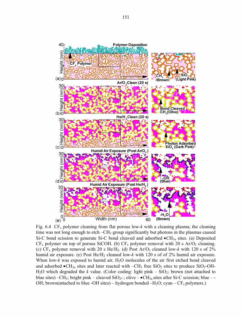
151
Fig. 6.4 CFx polymer cleaning from flat porous low-k with a cleaning plasma; the cleaning time was not long enough to etch –CH3 group significantly but photons in the plasmas caused Si-C bond scission to generate Si-C bond cleaved and adsorbed •CH3a sites. (a) Deposited CFx polymer on top of porous SiCOH. (b) CFx polymer removal with 20 s Ar/O2 cleaning. (c) CFx polymer removal with 20 s He/H2. (d) Post Ar/O2 cleaned low-k with 120 s of 2% humid air exposure. (e) Post He/H2 cleaned low-k with 120 s of of 2% humid air exposure. When low-k was exposed to humid air, H2O molecules of the air first etched bond cleaved and adsorbed •CH3a sites and later reacted with –CH3 free SiO2 sites to produce SiO2-OH-H2O which degraded the k value. (Color coding: light pink – SiO2; brown (not attached to blue sites) –CH3; bright pink – cleaved SiO2* ; olive – •CH3a sites after Si-C scission; blue – -OH; brown(attached to blue -OH sites) – hydrogen bonded –H2O; cyan – CFx polymers.)

152
Fig. 6.5 Preservation of the integrity of the low-k by surface pore sealing with Ar/NH3 plas-mas. (a) NH3 plasma sealed Ar/O2 cleaned profile where a 30s He plasma pre-treatment was used for surface activation before the sealing step. (b) NH3 plasma sealed He/H2 cleaned pro-file. (c) Ar/O2 cleaned, He activated and NH3 sealed profile after 120s of 2% humid air expo-sure. (d) NH3 sealed He/H2 cleaned profile after 120s of 2% humid air exposure. Ar/O2 plas-ma cleaned profile needs the He treatment before sealing but He/H2 plasma clean can itself activate the surface during the cleaning so no separate He pretreatment was required before sealing. After sealing, most of the pore openings in the surface were blocked by Si-N or C-N compounds and no significant water uptake was observed (blue sites indicate -OH) during humid air exposure. (Color coding: light pink – SiO2; brown (not attached to blue sites) –CH3; bright pink – cleaved SiO2* ; olive – •CH3a sites after Si-C scission; blue -OH; brown(attached to -OH blue sites) – hydrogen bonded –H2O; cyan – CFx polymers; olive-green (near porous surface) – Si-N and C-N compounds responsible for pore sealing.)

153
Fig. 6.6 Water uptake and k degradation by humid air in post-cleaned low-k for sealed and unsealed low-k. (a) Adsorbed water volume for sealed and unsealed low-k when exposed to humid air after the 20s polymer cleaning. (b) Degradation of low-k with time for sealed and unsealed profile as the 20s cleaned low-k was exposed to humid air. NH3 plasma sealing was able to block the pathways needed for the diffusion of H2O molecules of humid air; there was no significant water uptake and no significant low-k degradation after sealing.
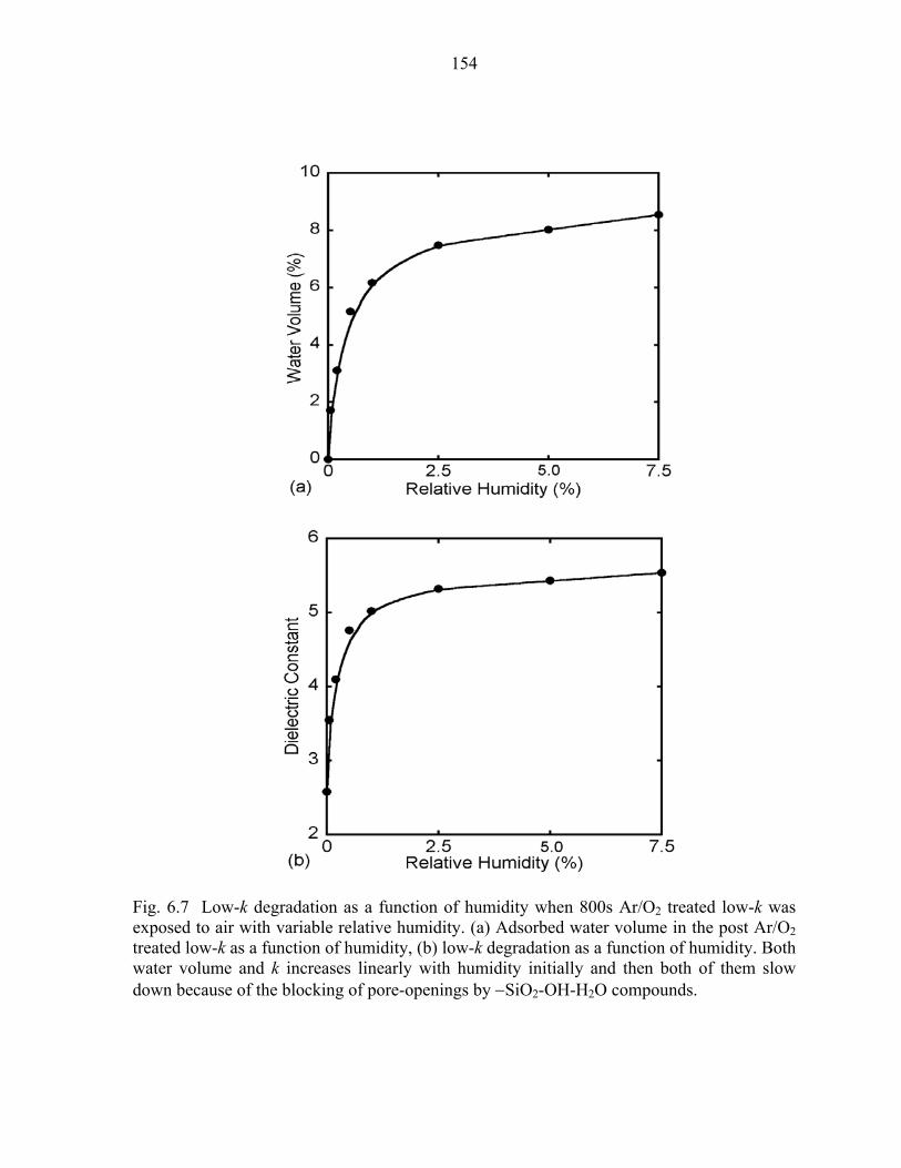
154
Fig. 6.7 Low-k degradation as a function of humidity when 800s Ar/O2 treated low-k was exposed to air with variable relative humidity. (a) Adsorbed water volume in the post Ar/O2 treated low-k as a function of humidity, (b) low-k degradation as a function of humidity. Both water volume and k increases linearly with humidity initially and then both of them slow down because of the blocking of pore-openings by −SiO2-OH-H2O compounds.
155
6.8 References
1. K. Maex, M. Baklanov, D. Shamiryan, F. Iacopi, S. H. Brongersma, K. Maex, and Z. S.
Yanovitskaya, J. Appl. Phys. 93, 8793 (2003).
2. M. R. Baklanov, K. P. Mogilnikov, and Q. T. Le, Microelectron. Eng. 83 2287 (2006).
3. G. Mannaert, M. R. Baklanov, Q. T. Le, Y. Travaly, W. Boullart, S. Vanhaelemeersch,
and A. M. Jonas J. Vac. Sci. Technol. B 23, 2198 (2005).
4. H. Seo, S. B. Kim, J. Song, Y. Kim, H. Soh, Y. C. Kim, and H. Jeon, J. Vac. Sci. Tech-
nol. B 20, 1548 (2002).
5. K. Sakuma, K. Machida, K. Kamoshida, Y. Sato, K. Imai, and E. Arai, J. Vac. Sci. Tech-
nol. B 13, 902 (1995).
6. M. A. Hartney, D. W. Hess, and D. S. Soane, J. Vac. Sci. Technol. B 7, 1 (1989).
7. D. Shamiryan, M. R. Baklanov, S. Vanhaelemeersch, and K. Maex, J. Vac. Sci. Technol.
B 20, 1923 (2002).
8. M. A. Worsley, S. F. Bent, S. M. Gates, N. C. M. Fuller, W. Volksen, M. Steen and T.
Dalton, J. Vac. Sci. Technol. B 23, 395 (2005).
9. K. Vanstreels, and A. M. Urbanowicz, J. Vac. Sci. Technol. A, 28, 173 (2010).
10. J. R. Woodworth, M. E. Riley, V. A. Amatucci, T. W. Hamilton, and B. P. Aragon, J.
Vac. Sci. Technol. A 19, 45 (2001).
11. B. Jinnai, S. Fukuda, H. Ohtake, and S. Samukawa, J. Appl. Phys. 107, 043302 (2010).
12. J. Lee and D. B. Graves, J. Phys. D 43, 425201 (2010).
13. H. Shi, J. Bao, R. S. Smith, H. Huang, J. Liu, P. S. Ho, M. L. McSwiney, M. Moinpour,
and G. M. Kloster, Appl. Phys. Lett. 93, 192909 (2008).
14. J. Proost, E. Kondoh, G. Vereecke, M. Heyns, and K. Maex, J. Vac. Sci. Technol. B 16,

156
2091 (1998).
15. J. Proost, M. Baklanov, K. Maex, and L. Delaey, J. Vac. Sci. Technol. B 18, 303 (2000).
16. M. Urbanowicz, M. R. Baklanov, J. Heijlen, Y. Travaly, and A. Cockburn, Electrochem.
Solid-State Lett. 10, G76 (2007).
17. A. M. Urbanowicz, D. Shamiryan, A. Zaka, P. Verdonck, S. De Gendt and M. R. Bak-
lanov, J. Electrochem. Soc. 157, H565 (2010).
18. F. N. Dultsev, A. M. Urbanowicz, and M. R. Baklanov, Mater. Res. Soc.
Symp. Proc. Vol. 1079 © 2008 Materials Research Society 1079-N07-03.
19. H.-G. Peng, D.-Z. Chi, W.-De Wang, J.-H. Li, K.-Y. Zeng, R. S. Vallery, W. E. Frieze,
M. A. Skalsey, D. W. Gidley, and A. F. Yee, J. Electrochem. Soc. 154, G85 (2007).
20. J. Shoeb and M. J. Kushner, “Damage by Radicals and Photons during Cleaning of Po-
rous Low-k SiOCH Part I: Demethylation in Ar/O2 and He/H2 Plasmas”.
21. M. J. Kushner, J. Phys. D 42, 194013 (2009).
22. A. Agarwal and M. J. Kushner, J. Vac. Sci. Technol. A 27, 37 (2009).
23. A. Sankaran and M. J. Kushner, J. Vac. Sci. Technol. A 22, 1242 (2004).
24. J. Shoeb and M. J. Kushner, J. Vac. Sci. Technol. A 29, 051305 (2011).
25. O. V. Braginsky, A. S. Kovalev, D. V. Lopaev, E. M. Malykhin, Yu. A. Mankelevich, T.
V. Rakhimova, A. T. Rakhimov, A. N. Vasilieva, S. M. Zyryanov, and M. R. Baklanov,
J. Appl. Phys. 108, 073303 (2010).
26. M.F.A.M. Van Hest, A. Klaver, D.C. Schram, and M.C.M. Van De Sanden, Thin Solid
Films 449 40 (2004).

157
27. M. Chaudhari, J. Du, S. Behera, S. Manandhar, S. Gaddam, and J. Kelber, Appl. Phys.
Lett. 94, 204102 (2009).
28. K. Singh, A. A. Kumbhar, and R. O. Dusane, Materials Letters 60 1579 (2006).
29. T. Kikkawa, S. Kuroki, S. Sakamoto, K. Kohmura, H. Tanaka, and N. Hata, Journal of
The Electrochemical Society, 152(7), G560 (2005).

158
7. MECHANISMS FOR PLASMA ETCHING OF HfO2 GATE-STACKS WITH Si SELECTIVITY AND
PHOTORESIST TRIMMING
7.1 Introduction
SiO2 has long served as the gate insulator for field-effect-transistors in very-large-
scale integrated circuits.[1] As feature sizes decrease, the gate-silicon dioxide equivalent
thickness required for the insulator also decreases.[2] A larger oxide capacitance (thinner
oxide layer) is necessary to invert the surface to a sufficient sheet charge density to obtain the
desired transistor current for a given supply voltage. Continuing to reduce the insulator
thickness using SiO2 is problematic as leakage currents due to tunneling increase as the
thickness approaches a monolayer.[1] Consequently, high dielectric constant (high-k) metal
oxides, and HfO2 in particular, are being implemented as replacements for SiO2 in gate-
stacks to minimize leakage current resulting from thinning of the insulator. The larger die-
lectric constant allows the oxide to be thicker for a given capacitance, thereby decreasing
electric fields and leakage currents.
A high-k dielectric and a poly-Si gate are typically not suitable for high performance
logic as the combination has a higher threshold voltage and lower channel mobility, and so a
poor drive current.[1] Metal gates, having a higher free carrier density, maintain a high mo-
bility at junctions with high-k dielectrics and so many advanced designs incorporate metal
gates.[1] TiN is one such metal being considered for the gate.[3] Given other technology
requirements, such as back-anti-reflection coatings (BARC) to maintain critical dimensions
(CD) during lithography, the gate-stack prior to etching can contain many layers and materi-
als, as schematically shown in Fig. 7.1.

159
To speed the plasma processing of gate-stacks, it is desirable to etch the entire stack
using a single process. This requires a high selectivity for the oxide, in this case HfO2, with
respect to the underlying Si layer. (That is, the HfO2 will be etched but the underlying Si will
not be etched.) It has been found that similar gate-stacks can be etched using BCl3/Cl2 plas-
mas while having a good selectivity to underlying Si by forming a BCln polymer on the Si
which slows its etching.[4]
In this chapter, the plasma etching of HfO2 gate-stacks is computationally investigated
with an emphasis on the selectivity between HfO2 and Si. The model gate-stack consists of
photoresist (PR), BARC, TiN, HfO2, SiO2 and the underlying Si. (See Fig. 7.1.) This gate-
stack is based on industrial test structures. Reaction mechanisms for etching of TiN and
HfO2 were developed for plasmas sustained in Ar/BCl3/Cl2 mixtures. Trimming of the PR to
achieve narrower linewidths was also addressed. The Hybrid Plasma Equipment Model
(HPEM) was employed to simulate the reactor scale and surface kinetics for inductively and
capacitively coupled plasma tools. The model reactor is an inductively coupled plasma (ICP)
having a radio frequency (rf) bias on the substrate. The mechanisms were then implemented
in the Monte Carlo Feature Profile Model (MCFPM) with which etch profiles are predicted.
Validation was performed with data from literature.
We found that BCln species produced by electron impact in the plasma react with
HfO2, which, under ion impact, form volatile etch products such as BmOCln and HfCln. Se-
lectivity to Si is achieved by creating Si-B bonding as a precursor to the deposition of a BCln
polymer, which slows the etch rate relative to HfO2. The low ion energies required to
achieve this selectivity then challenge one to obtain highly anisotropic profiles in the metal
gate portion of the stack.

160
The models used in this investigation are briefly described in Sec. 7.2, followed by a
discussion of the reaction mechanisms in Sec. 7.3. Photoresist trimming and BARC etching
are discussed in Sec. 7.4. Plasma properties and HfO2 etch characteristics are discussed in
Sec. 7.5 followed by our concluding remarks in Sec. 7.6.
7.2 Description of the Models
The HPEM was used to predict the reactor scale plasma characteristics and reactant
fluxes to surfaces in the ICP reactor. The HPEM has been previously described and so is on-
ly briefly summarized here.[5] The HPEM is a two-dimensional (2d), modular model which
addresses gas phase and surface kinetics. Electromagnetic fields are derived by solving the
frequency domain wave equation based on coil currents adjusted to deliver a specified power
deposition. The spatially dependent power deposition is used as a source term in obtaining
the electron temperature, Te, from an electron energy conservation equation. Transport and
rate coefficients as function of average electron energy are obtained from a solution of
Boltzmann’s equation, and a Monte Carlo simulation is used to follow the trajectories of
sheath accelerated secondary electrons. The transport coefficients and source functions are
used by the fluid kinetics module (FKM) to solve separate continuity, momentum, and ener-
gy equations for each ion and neutral species, while semi-implicitly solving Poisson’s equa-
tion for the time varying electrostatic potential. The densities and electrostatic fields from
the FKM are then transferred to the other modules. This process is iterated until a converged
quasi-steady state solution is obtained.
Reaction probabilities for gas phase species with surfaces are provided by the surface
chemistry module (SCM) which computes the composition of surface resident species using

161
a multilayer surface-site-balance model. The reaction mechanism is unique for each surface
in contact with the plasma. The plasma chemistry Monte Carlo module (PCMCM) produces
the energy and angular distributions for neutrals and ions striking surfaces in contact with the
plasma. The PCMCM launches pseudoparticles representing ions and neutrals based on the
electron impact source functions. Using time dependent electric fields from the FKM, their
trajectories are integrated while accounting for gas phase collisions. The energy and angular
distributions (EADs) of ion (IEADs) and neutral pseudoparticles are recorded as they strike
surfaces.
The SCM and MCFPM incorporate energy dependent reaction probabilities based on
the EADs obtained from the PCMCM. The probabilities for surface reactions involving en-
ergetic species (either ions or hot neutrals) are given by [6]
p(E) = p0 mt
mr
mt
m
EEEE
−− (7.1)
where p(E) is the reaction probability for a particle with energy E, Et is the threshold energy
of the process, Er is a reference energy, and po is the reaction probability at the reference en-
ergy. We used m = 0.5 for sputtering or ion activated etching.
The 2d MCFPM has been previously described and so is briefly summarized here.[7]
The MCFPM predicts the evolution of surface morphology and profiles based on the fluxes
and EADs from the HPEM. The MCFPM resolves surface materials using a 2d rectilinear
mesh where each cell in the mesh is assigned a material identity. Gas phase species are rep-
resented by pseudoparticles and surface species are represented by computational mesh cells.
162
Pseudoparticles are launched towards the surface from random locations above the wafer
with energies and angles sampled from the EADs. The trajectories of the pseudoparticles are
tracked until they hit a surface, where a generalized surface reaction mechanism controls the
interaction. The identity of the material mesh cell is changed (representing a surface chemi-
cal reaction), removed (etching) or a cell is added (deposition) as dictated by the reaction
mechanism. Gas phase pseudoparticles are reflected or emitted from the surface consistent
with the mechanism.
The ICP reactor used in this study is schematically shown in Fig. 7.2(a). The cylin-
drical chamber is 13 cm in radius and 17 cm in height. The inductive power is supplied
through a three-turn antenna coil above a 0.8-cm-thick quartz window. The wafer is on an
independently powered substrate 9 cm below the quartz window. For gate-stack etching, the
300 W ICP was sustained in Ar/BCl3/Cl2 = 5/40/55 at 5 mTorr with a flow rate of 100 sccm.
The gas phase reaction mechanism is listed in Table 7.1. The wafer size used in this simula-
tion was 150 mm, however, the etching mechanisms discussed here are independent of wafer
size.
The high-k gate-stack used for the simulation, as shown in Fig. 7.1, consists of a 290
nm thick erodible photoresist mask, 40 nm thick BARC layer, 160 nm thick TiN, 20 nm
HfO2, 10 nm SiO2 (to improve carrier mobility in the channel) and the Si substrate. The sub-
strate bias voltage was varied to investigate the effect of ion energy on the selectivity of HfO2
with respect to Si.[4,8] Extensive parameterizations were performed to determine the effects
of the probabilities of polymer formation, polymer sputtering and Si-B bond formation on
selectivity. Parameterizations were also performed to determine whether the proposed mech-
anism is sensitive to the device layout. For example, the default gate-stack pitch (the full dis-

163
tance between the center of gate-stacks) of 200 nm was decreased to 150 nm and increased to
300 nm. The scaling laws discussed here were insensitive to those variations.
7.3 Surface Reaction Mechanism for Gate-stack Etching
7.3.1 Etching of HfO2
Previous investigations of the plasma etching of metal oxides were used to develop
our reaction mechanism. Sha et. al investigated the etching of high-k ZrO2 in BCl3/Cl2 plas-
mas which shares many etch characteristics with HfO2.[8] They concluded that BCl2+ ions
play an important role in removing O atoms from ZrO2, as volatile B2OCl4, B3O2Cl5 and
(BOCl)3. These processes, with the formation of a Si-B passivation layer, enabled a ZrO2 to
Si selectivity of 10 at ion energies near but above the threshold for ZrO2 etching. They also
found that in BCl3/Cl2 plasmas, HfO2 and ZrO2 etch rates are dependent on the BCl2+ density
that is responsible for O-atom removal, the Cl density which is responsible for Hf passivation
to eventually remove Hf as HfCln (n = 2-4), and on the bond strength of the metal-oxygen
bond.[9] By operating with ion energies slightly above the etching threshold for the metal
oxide, HfO2 to Si selectivity can be obtained.
TaN/HfO2 gate-stacks have been etched employing Ar/BCl3/O2 plasmas to obtain
high TaN/HfO2 selectivity.[10] However with the presence of oxygen species in these plas-
mas, the Si-B passivation layer thought to be responsible for high HfO2/Si selectivity is diffi-
cult to maintain. This results in a lower HfO2/Si selectivity as compared to etching in
Ar/BCl3/Cl2 plasmas. Wang et. al investigated etching of HfO2 and poly-Si in BCl3 plasmas
as a function of substrate temperature as a function of source power in a helicon reactor.[11]
BCl2 and Cl were found to be the dominant gas phase radicals at all powers investigated,
164
which is consistent with our findings. They found that selectivity of HfO2 over Si was en-
hanced at low power and low substrate temperature. Nakamura et. al etched HfO2 films in
BCl3-containing plasmas employing an electron cyclotron resonance (ECR) reactor without
rf biasing.[12] For BCl3/Cl2 = 40/60 mixtures, a HfO2/Si selectivity of approximately 10 and
an etch rate of 1000 A/min were obtained. Our simulation results are in reasonable agree-
ment with their findings.
When modeling plasma etching of new materials such as HfO2, the fundamental ex-
perimental data base required to develop the mechanism is often fragmentary. When both
mechanisms and rates are not available, modeling and developing a reaction mechanism be-
gins with examining the current databases for experimental results for etch rates and selectiv-
ity, material thermodynamic properties, and mechanisms and reaction probabilities for analo-
gous processes, as well as theoretical expressions for general scaling laws. Based on these
analyses, a sequence of reactions is proposed and probabilities assigned for bond breaking,
adsorption and etching reactions (that is, the mechanism is built). Extensive parameteriza-
tions and sensitivity analyses are then required to refine the mechanism to well represent the
etch rates, threshold energies and selectivities available from the literature. This is done
while acknowledging that there are always risk of uncertainties in building such a mecha-
nism.
Following these procedures while benefiting from the insights provided by previous
works, a mechanism was developed for etching HfO2 in Ar/BCl3/Cl2 plasmas. In our mecha-
nism the etching of HfO2 incorporates two distinct steps – removal of Hf and of O. While
Cl2 plasmas can etch HfO2 forming volatile HfCln and ClO species as a result of Cl adsorp-
tion and ion impact, selectivity for HfO2 with respect to Si cannot necessarily be insured.[13]

165
This is the fundamental motivation for using BCl3/Cl2 plasmas. Electron impact dissociation
of BCl3 produces BCln (n = 1,2) species which have the ability to form volatile etch products
such as B2OCl3, B2OCl4, BOCl, (BOCl)3 and B3O2Cl5. These species also have the ability to
inhibit Si etching through formation of a BCln polymer.
In our mechanism, HfO2 etching is initiated by the breaking of the Hf-O bonds, each
having bond strength of approximately 8.3 eV. By analogy with other processes and through
parametric studies, a threshold energy of 14 eV was assigned to the Hf-O bond breaking step.
The first such process breaks one Hf-O bond in HfO2, and so generates HfO(s) and O(s),
where (s) denotes a surface resident species. A second above threshold ion can break the re-
maining Hf-O bond in HfO(s) to produce O(s) and Hf(s). The exposed Hf(s) sites are subse-
quently passivated by Cl to produce HfCln(s) (n = 1-4) and ultimately a volatile etch product
HfCln(g) following ion impact. (Note that at low temperatures, HfCl4 may be formed as a
loosely adhered non-volatile product that requires ion activation for removal.)
Exposed HfO(s) sites are passivated by Cl(g) leading to the formation of HfOCl(s)
and HfOCl2(s). The Hf atom in HfOCl(s) and HfOCl2(s) can be removed in a single step by
ion impact as volatile HfCln(g) leaving behind O(s) with a dangling bond on the surface.
Although the probability is small, Cl(g) can adsorb on HfO2(s) forming solids such as
HfO2Cl(s) and HfO2Cl2(s). The first Hf-O bond in these species can be broken by ion bom-
bardment producing nonvolatile HfOCl(s) and HfOCl2(s).
The full reaction mechanism for Hf(s) removal is listed in Table 7.2 and, in summary,
is
M+(g) + HfO2(s)→ HfO(s) + O(s) + M(g), (7.2)

166
M+(g) + HfO(s) → Hf(s) + O(s) + M(g), (7.3)
Cl(g) + HfCln-1(s) → HfCln(s) (n=1,3) (7.4)
M+(g) + HfClx(s) → HfCln(g) + M(g) (7.5)
Cl(g) + HfO(s) → HfOCl(s), (7.6)
M+(g) + HfOClx(s) → O(s) + HfCln(g) + M(g), (7.7)
where M+(g) represents an ion.
To remove bonded oxygen on the surface, the site can adsorb BCln(g) (n=1,2) form-
ing OBCln(s). These complexes can then be removed by ion bombardment. The bonded ox-
ygen can also be removed directly by BCln+(g) (n= 1,2) bombardment as either as B2OCl4(g)
or B2OCl3(g). A second process for removing bonded O is initiated by BCln+(g) directly
striking HfO2(s) producing OBCl2(s) and OBCl(s). The OBCl(s) can be etched by energetic
ions as volatile BOCl(g), and producing OBCl2(s). The latter can be removed by the previ-
ously described mechanism. The full reaction mechanism for O(s) removal is listed in Table
7.2 and in summary is
BCln(g) + O(s) → BClnO(s), (7.8)
BCln+(g) + HfO2(s) → BClnO(s) + HfO(s), (7.9)
M+(g) + BClnO(s) → BmOClp(g). (7.10)
One of the motivations to include BCl3 in the gas mixture is to improve the selectivity
for HfO2 with respect to Si. Formation of a BCln passivation layer on the Si is believed to
play an important role in obtaining this selectivity by slowing the Si etch rate. The pas-

167
sivation layer is proposed to form in two steps. The first is forming Si-B bonds by adsorption
of BCln to create a base layer. The second is polymer deposition by BCln(g) on the base lay-
er.[4]. The polymerization reaction mechanism is listed in Table 7.3, and is summarized as,
BCln(g) + Si(s) → SiBCln(s), (7.11)
BCln(g) + SiClm(s) → SiClmBCln(s), (7.12)
BCln(g) + SiBClm(s) → SiBCln(s)-P(s), (7.13)
BCln(g) + SiClmBCln(s) → SiClmBCln(s)-P(s), (7.14)
M+(g) + P(s) → P*(s) + M(g), (7.15)
BCln(g) + P(s)* → P(s)* + P(s), (7.16)
M+(g) + P(s) → BCl2(g) + M(g), (7.17)
where P(s) is the polymer and P*(s) is an activated state of the polymer generated by low en-
ergy ion bombardment with enhanced deposition rates. Although not strictly stoichiometri-
cally correct, sputtering of the polymer produces BCl2(g) which can redeposit. As such there
are two competing processes – higher ion energies increase the rate of etching of the HfO2
while also increasing the rate of sputtering of P(s) on the Si which decreases selectivity.
7.3.2 TiN Etching
TiN(s) etching begins with ion bombardment to break the Ti-N bond and liberate N
atoms. The Ti(s) site then adsorbs Cl(g) leading to the formation of TiCln(s) (n= 1-3). Ion
bombardment removes these compounds as TiCln(g).[26] TiN(s) can itself adsorb Cl(g) to
produce TiNCl(s) followed by energetic ion bombardment containing Cl to directly remove

168
Ti from TiNCl(s) as volatile TiCln(g). In an integrated gate-stack etching process, the PR
may be trimmed and BARC removed in plasmas producing O atoms. When the TiN surface
is exposed to both energetic ions and O atoms, Ti-N bond breaking followed by O atom ad-
sorption can form nonvolatile TiO(s). When then etching the gate-stack in Ar/BCl3/Cl2
plasmas, TiO(s) adsorbs Cl(g) forming TiOCln(s) (n=1, 2). Ions striking these oxichlorides
can then be removed as volatile TiOCln(g) (n=1, 2) by ion bombardment. The reaction
mechanism for TiN(s) etching is listed in Table 7.4 and is summarized as,
M+(g) + TiN(s) → Ti(s) + N(g) + M+(g), (7.18)
Cl(g) + TiCln-1(s) → TiCln(s), (n=1,3) (7.19)
M+(g) + TiCln(s) → TiCln(g) + M(g), (n = 1-3) (7.20)
Cl(g) + TiCl3(s) → TiCl4(g). (7.21)
7.3.3 Photo-resist trimming, BARC etching and PR erosion
As gate length shrinks below 50 nm, 193 nm lithography is challenged to directly de-
fine the features.[27-29] Consequently, when the width of the PR line after lithography is
larger than the desired dimensions, trimming of the PR is often employed. For organically
based PR, controlled exposure to an O2 containing plasma will etch back the PR to a smaller
dimension. Such plasmas may also reduce the sidewall roughness of the PR. For example,
Sin et. al investigated trimming of PR and etching of BARC in an integrated step employing
CF4/O2 plasmas.[26] The oxygen provided a high PR removal rate while the polymerizing
CF4 maintained a vertical PR/BARC profile after trimming.[27] Although the trim rate is
higher for CF4/O2 plasmas compared to Cl2/O2 and HBr/O2 plasmas, the amount of oxygen

169
found on the PR sidewall after trimming is higher.[28] In spite of its slow trim rate, precise
control of the CD during trimming has been obtained using Cl2/O2 plasmas. [28,29] It has
also been shown that Ar/O2 plasmas generate a vertical and uniform PR profile with a high
PR removal rate.[30]
To simulate the full gate-stack etching process, we included a PR-trim step prior to
exposure to the Ar/BCl3/Cl2 plasma. The PR-trim step was performed in an Ar/O2 plasma
which also served to remove the BARC layer. The intent of the trim process was to reduce
the initial photo-resist having a height of 290 nm and width of 58 nm to a width of 32 nm.
As both BARC and PR are primarily hydrocarbons, they can be chemically etched by
plasma produced oxygen species such as, O(g), O+(g) and O2+(g) and chemically sputtered by
the ions. The reaction mechanism for Ar/O2 plasma etching of the organic PR and BARC is
listed in Table 7.5, and is summarized as follows. (Note that COH(g) is a generic PR and
BARC etch product which can redeposit as a PR or BARC species but is otherwise unreac-
tive in the plasma.)
M+(g) + PR(s) → PR(g) + M+(g), (7.22)
M+(g) + BARC(s) → BARC(g) + M+(g), (7.23)
O(g) + PR(s) → COH(g), (7.24)
O(g) + BARC(s) → COH(g), (7.25)
On+(g) + PR(s) → COH(g), (7.26)
On+(g) + BARC(s) → COH(g). (7.27)
If the BARC is completely cleared during the PR-trim, ions in the Ar/O2 plasma can

170
break Ti-N bonds to produce Ti(s) sites which then adsorb O(g) to produce TiO(s). During
the gate-stack etch in Ar/BCl3/Cl2 plasmas, the TiO(s) sites can further adsorb Cl(g) to pro-
duce TiOCl(s) and TiOCl2(s). Ions in the Ar/BCl3/Cl2 plasma remove these species as vola-
tile TiOCl(g) and TiOCl2(g). A summary of the reactions for TiO(s) and TiOCln(s) (n = 1,2)
formation and removal are (See Table 7.4),
M+(g) + TiN(s) → Ti(s) + N(g) + M+ (g), (7.28)
O(g) + Ti(s) → TiO(s), (7.29)
Cl(g) + TiO(s) → TiOCl(s), (7.30)
Cl(g) + TiOCl(s) → TiOCl2(s), (7.31)
M+(g) + TiOCln(s) → TiOCln(g) + M+(g), n=1,2 (7.32)
There will be a tradeoff between fully removing the BARC and exposing the TiN to the oxy-
gen plasma and leaving a thin BARC later that must be removed during the gate-stack etch.
The process conditions for the PR-trimming and BARC etching were 5 mTorr,
Ar/O2=5/95 gas mixture with a flow rate of 100 sccm. The coil delivered 300 W at 10 MHz.
A bias of 18 V was applied to the substrate. Probabilities for BARC and PR etching were
varied to determine the values required to maintain an acceptable CD while also trimming the
PR. It was found that when the BARC etch rate is 1.5 times higher than the PR etch rate,
these goals are met. For example, post-trim gate-stack profiles with relative etching proba-
bilities between the BARC and PR of 1.5, 1.0 and 0.5 are shown in Fig. 7.3. With the BARC
etch rate 1.5 times that of the PR, a good CD was obtained however a small amount of
BARC was left on the TiN which produced micro-masking during the etch steps. When the
171
PR and BARC etch rates are equal, the PR width shrank below 25 nm and a 5-10 nm layer of
BARC micro-masking was left on the TiN. Leaving this layer would require more time in
the gate-stack etch step to clear the BARC due to the absence of O species in the Ar/BCl3/Cl2
plasma. To totally clear the BARC during the trim would produce an unacceptably narrow
PR.
7.4. Plasma and HfO2 Etch Properties
The process conditions for the gate-stack etch were a 5 mTorr Ar/BCl3/Cl2=5/40/55
gas mixture with a flow rate of 100 sccm. The coil delivered 300 W at 10 MHz. The ampli-
tude of the 13.56 MHz rf bias on the substrate was varied. The total ion density was 3.2 ×
1011 cm-3. BCl2+ has the highest density (1.6 × 1011 cm-3) followed by Cl+ (1.0 × 1011 cm-3).
Cl is the radical with the largest density (1.0 × 1014 cm-3) followed by BCl2 (1.3 × 1013 cm-3).
(See Fig. 7.2.) Fluxes of the major ions and neutral radicals to the substrate are shown in Fig.
7.4 for the base case with a 32 V substrate bias. The dominant radical fluxes are Cl (1 × 10¹⁸
cm-2s-1) and BCl2 (7.5 × 1016 cm-3s-1). Cl is produced by both electron impact dissociation of
Cl2 and BCl3, the latter yielding BCl2 and Cl. Electron-impact ionization of BCl3 dominantly
produces BCl2+ and Cl. The major ion fluxes are BCl2
+ (8 × 1015 cm-2s-1), Cl+ (4 × 1015 cm-
2s-1), Cl2+ (4 × 1014 cm-2s-1) and Ar+ (4 × 1013 cm-2s-1). The low flux of Ar+ results from the
low mole fraction of Ar but also from rapid charge exchange reactions to other species. With
a 32 V bias, the average energy for all ions incident on the substrate is near 30 eV with an
angular spread from the vertical of < 150, as shown by the IEADs in Fig. 7.5.

172
7.5 HfO2 Etch Rate vs. Bias Voltage
Bias voltage affects the properties of the gate-stack etch through rate, profile and se-
lectivity of HfO2 to Si. The post-etch gate-stack profiles for biases of 32, 60 and 100 V are
shown in Fig. 7.6a for equal etch times corresponding to when the 32 V bias removes the
SiO2 layer. Etch rate and selectivity as a function of bias voltage are shown in Fig. 7.6b.
The etch rate of HfO2 has a threshold bias of 27 V increasing from 100 Å/min at 32 V to 650
Å/min at 200 V. The increase in etch rate slows above 100 V as the rates of increase in ion
activated reaction probabilities begin to saturate. The increase in etch rate comes at the ex-
pense of selectivity. The selectivity is as large as 12 at a bias of 32 V, decreasing monoton-
ically to 2 for a bias of 200 V. The decrease in selectivity is largely a consequence of the
removal of polymer on the Si by sputtering.
Our predicted threshold of 27 V for HfO2 etching is in agreement with the experimen-
tally measured threshold of 28 V.[9,13] The predicted high selectivity near the etching-
threshold is corroborated by experimental results where highly selective etching of HfO2 lay-
er over Si was achieved by control of the substrate bias.[4,13] The predicted decrease in se-
lectivity as a function of increasing bias is also in general agreement with experiment, though
our decrease in selectivity is more gradual.[13]. Predicted HfO2 etch rates for biases of 32-
200 V bias are also in general agreement with experiment, with differences attributable to
differences in the total fluxes of reactants in the reactors used by different research-
ers.[4,12,13]
The increase in bias voltage also produces undercutting of the TiN. In spite of a nar-
rowing of the IEAD with increasing bias, there is still sufficient width to produce some lat-
eral etching due to the open field on both sides of the feature. This is an affect that would not

173
be as apparent in trench or via etching where at higher aspect ratios the ions at broader angles
are shadowed.
Gate-stack profiles at the time when the SiO2 layer is cleared for each bias are shown
in Fig. 7.7a for 32, 60 and 100 V. Using a qualitative assessment of maintaining CD (that is,
a vertical profile) while minimizing Si damage, the best profiles obtained for 32, 60 and 100
V biases as a function of over-etch time are shown in Fig. 7.7b. The high HfO2/Si selectivity
afforded by the 32 V bias allows a sufficient over-etch to produce a largely uniform gate-
stack width. There is little damage to the Si substrate although there is a small narrowing of
the TiN. The lower selectivity obtained with a 60 V bias produced some damage to Si layer
while the gate-stack has less narrowing. This damage is, in part, due to the initial micro-
masking of the TiN by the BARC and TiO which ultimately produces different clearing times
to the Si at different locations. Those TiN sites that are micro-masked have a delayed start to
etching corresponding to when the masking material (BARC or TiO) is removed. Although
the BARC and TiO that produce micro-masking are more rapidly removed with the higher
bias, thereby reducing the negative aspects of micro-masking, the etch rates of the TiN, HfO2
and SiO2 are also more rapid with increasing bias. This leads to over-etching at random sites
on the Si that were not micro-masked. Further etching to remove the tapering in the gate-
stack then produces more Si damage. These trends are intensified with the 100 V bias; as
both the HfO2/Si selectivity decreases and the CD worsens (narrowing of the gate-stack.).
Both an acceptable CD and HfO2/Si selectivity were obtained with a 32 V bias where
the TiN and HfO2 had a nearly consistent width of 32 nm. A slight tapering of the TiN and
HfO2 occurred for the 60 V bias with a small amount of damage to the Si. The profile could
not be optimized for both width and lack of damage to the Si at 100 V. For example, the TiN

174
narrowed to a width of below 25 nm, with there being significant erosion of the Si substrate.
As discussed above, depending on the ratio of the PR to BARC etch rates during the
PR-trim step, there may be micro-masking on the TiN at the end of the trim step due to in-
complete removal of the BARC. In practice, the remaining BARC layer is often removed
with an intermediate plasma etching step prior to the gate-stack etch to eliminate the possibil-
ity of micro-masking. In the absence of the BARC removal step, the micro-masking material
is dominantly removed by sputtering reactions during the gate-stack etch, which also serves
to further erode the PR. For example, while clearing the micro-masking layer and etching
the gate-stack in the base case, the PR width was further reduced by a few nm. Sites under-
neath the micro-masking etch more slowly due to the prior need to remove the BARC by
sputtering. For example, time sequences of the gate-stack profile with biases of 32 and 100
V are shown in Fig. 7.8 with BARC micro-masking remaining from the PR-trim. If the se-
lectivity of HfO2/Si is high enough, as with the 32 V bias, the different clearing times of the
TiN and HfO2 laterally across the feature due to micro-masking are not detrimental to either
the final CD or selectivity. For low selectivity conditions, as with the 100 V bias, the micro-
masking is problematic as the over-etch results in local sites on the Si being damaged.
A quantitative measure of CD is the slope of the gate-stack profile where 90° would
indicate a vertical profile. The slope of the gate-stack profile is shown in Fig. 7.9 for differ-
ent biases as a function of over-etch time. The beginning of the over-etch is when the SiO2
on top of Si substrate is cleared. The asymptotic slope at long over-etch is 80°-90° with
higher biases both achieving a slope nearer the vertical and achieving that slope with shorter
over-etch times. These more optimum slopes are obtained at the expense of poor selectivity.

175
7.5.1 Selectivity: Si-B Bond Formation
The selectivity of HfO2 to Si depends on the formation and persistence of the BCln
polymer layer. To determine the sensitivity of selectivity to rates of Si-B bond formation,
polymer deposition and polymer sputtering, the probabilities for these processes were param-
eterized in the model.
Selectivity while varying the probability of the Si-B bond formation that initiates the
deposition of polymer is shown in Fig. 7.10a for different bias voltages. The corresponding
gate-stack profiles are shown in Fig. 7.11a. In the absence of Si-B bond formation, the pol-
ymer does not deposit, and so the selectivity is based only on the intrinsic etch rates of the
HfO2 and the Si, which for the base case conditions are nearly equal. As the probability for
Si-B bond formation increases from 0 to 0.4, the rate of etching of Si slows and the selectivi-
ty improves to 10 for a bias of 32 V. At this probability, the majority of the available sites
are passivated and covered by BCln polymer. Although selectivity increases with increasing
bond formation probability for all biases, as the bias voltage and sputtering rates increase, the
residence time of Si-B bonding decreases and so the rate of polymer formation also decreas-
es. The end result is a decrease in selectivity with bias voltage. For example, for a bias of
100 V, only 45% of the Si sites are, on the average, passivated.
The gate-stack profile prior to reaching the Si layer is essentially independent of the
Si-B bond formation probability for a given etch time. The consequences of Si-B bonding
are only felt once the SiO2 layer is cleared. With a low Si-B bond formation probability,
sites on the Si are periodically exposed to the plasma, producing roughness and damage, as
shown in Fig. 7.11a. Increasing the bond formation probability insures that these sites are
nearly continuously passivated, thereby reducing the propensity for damage.
176
7.5.2 Selectivity: Polymer Deposition
Provided that Si-B bonds are present, BCln(g) species adsorb on top of Si-B com-
pounds to form BCln polymers.[4] Selectivity as a function of polymer deposition probability
and interface properties for different bias voltages are shown in Fig. 7.10b and Fig. 7.11b.
As the probability for polymer deposition is increased from 0 to 0.5, the selectivity improves
from 3 to 10 for a bias of 32 V. The selectivity is almost constant at probabilities higher than
0.5. Selectivity is above 2 for all biases even in the absence of polymer formation as the Si
etch rate is slowed by the base layer of Si-B bonding. As the bias voltage increases, the rates
of sputtering of the polymer and Si-B bond breaking increase resulting in a lower selectivity.
Increasing the bias to 100 V reduces selectivity by nearly half at all deposition probabilities.
Again, the gate-stack profile is independent of the polymer formation rate, though the rough-
ness and damage to the Si layer increases with increasing bias, as shown in Fig. 7.11b.
7.5.3 Selectivity: Polymer Sputtering
As the polymer is deposited, it is also necessary that the polymer be sustained in order
to obtain high selectivity. Higher polymer sputtering rates produce thinner polymer layers
and so results in lower selectivity. For example, selectivity as a function of the polymer sput-
tering probability (this is the probability at the reference energy of 140 eV) is shown in Fig.
7.10c for biases of 40, 100 and 150 V bias. Gate-stack profiles for different polymer sputter-
ing probabilities are shown in Fig. 7.12. Selectivity decreases with increasing polymer sput-
tering probability while the Si roughness and damage increase.
177
7.6 Concluding Remarks
PR/BARC/TiN/SiO2/Si gate-stack etching employing Ar/BCl3/Cl2 plasmas preceded
by an Ar/O2 plasma PR-trim and BARC removal was computationally investigated. HfO2
etching likely requires breaking of Hf-O bonds and separate removal of Hf(s) and O(s) atoms
by Cl(g) adsorption and ion assisted etching. Etching of TiN likely includes breaking of Ti-
N bonds and chlorination of Ti(s) to be removed as TiCln(g). The model confirms that
HfO2/Si selectivity can be achieved by deposition of a BCln polymer on the Si, preceded by
Si-B bond formation. With low biases, selective etching of HfO2 with respect to Si can be
achieved while minimizing undercutting of the TiN gate due to the persistence of the poly-
mer layer. A significant over-etch, however, is required to achieve the optimum etch profile
(that is, closest to 90°). While higher bias voltages require less time to achieve a profile
slope close to 90°, this is achieved at the cost of selectivity. The role of Si-B bond formation
and growth of BCln polymer were parametrically investigated. We found that both Si-B
bond formation and polymer deposition are necessary to achieve high selectivity though
some nominal selectivity is afforded by the Si-B bonding.
Optimizing the PR-trim prior to the gate-stack etch involves a tradeoff between
maintaining the CD of the PR and total removal of the BARC. This tradeoff results from the
PR and BARC both typically being organics having similar etch rates in oxygen containing
plasmas. Parameterization showed that a BARC etch rate 1.5 times higher than that of the
PR provides the best post-trim profile. A thin layer of BARC left on the TiN produces mi-
cro-masking which must first be removed during the gate-stack etch. At low bias voltages,
this micro-masking was not necessarily detrimental to the final gate-stack profile and did not
significantly contribute to damaging the Si due to the need to over-etch. These trends result-

178
ed from the high HfO2/Si selectivity at low bias voltages that protects the Si substrate sites
during even a long over-etch.
Although the reaction mechanism we developed does reproduce experimental trends,
there are uncertainties in both the sequence of reactions and in reaction probabilities. For
example, our studies have shown the range of probabilities for important processes, such as
for sputtering and polymer deposition, over which predicted etch rates and selectivity are
most sensitive. The test of the mechanism is whether it provides accurate predictions for
process conditions considerably different from that used to help create the mechanisms. As
such refinement of the mechanism will benefit from further comparisons to experiments.

179
7.7 Tables
Table 7.1 Ar/BCl3/Cl2 Gas Phase Reaction Mechanism
Species:
Ar, Ar*, Ar+, e Cl2, Cl2
+, Cl, Cl*, Cl+, Cl- BCl3, BlC2, BCl3
+, BlC2+
Reaction Rate Coefficient Reference
e + Ar → Ar + e f(ε)a 14
e + Ar → Ar* + e f(ε)a 15
e + Ar → Ar+ + e + e f(ε)a 16
e + Ar* → Ar+ + e + e f(ε)a 17
e + Ar* → Ar + e f(ε)a 18
e + Cl2 → Cl2 + e f(ε)a 19
e + Cl2 → Cl2(v) + e f(ε)a 19, c
e + Cl2 → Cl + Cl- f(ε)a 19
e + Cl2 → Cl + Cl + e f(ε)a 19
e + Cl2 → Cl2+ + e + e f(ε)a 19
e + Cl → Cl + e f(ε)a 19
e + Cl → Cl* + e f(ε)a 19
e + Cl → Cl+ + e + e f(ε)a 19
e + Cl* → Cl* + e f(ε)a 19
e + Cl* → Cl + e f(ε)a 19

180
Table 7.1 (Continued)
e + Cl* → Cl+ + e + e f(ε)a 19
e + Cl- → Cl + e + e f(ε)a 19
e + Cl2+ → Cl + Cl 1 x 10⁻⁷/Te
0.5 b
e + BCl3 → BCl3 + e f(ε)a b
e + BCl3 → BCl3(v) + e f(ε)a 20
e + BCl3 → BCl2 + Cl- f(ε)a 20
e + BCl3 → BCl2 + Cl + e f(ε)a 21
e + BCl3 → BCl3+ + e + e f(ε)a 21
e + BCl3 → BCl2+ + Cl + e + e f(ε)a 21
e + BCl3+ → BCl2 + Cl 1 × 10⁻⁷/ Te
0.5 22, b
e + BCl2 → BCl2 + e f(ε)a d
e + BCl2 → BCl2(v) + e f(ε)a c, d
e + BCl2 → BCl2+ + e + e f(ε)a 23
e + BCl2+ → BCl2 1 × 10⁻⁷/ Te
0.5 22
Cl* → Cl 1 × 10⁵ b
Cl- + Cl+ → Cl + Cl 1 × 10⁻⁷ b
Cl- + Cl2+ → Cl2 + Cl 1 × 10⁻⁷ b
Cl- + Ar+ → Cl + Ar 1 × 10⁻⁷ b
Cl- + BCl2+ → BCl2 + Cl 1 × 10⁻⁷ b
Cl- + BCl3+ → BCl3 + Cl 1 × 10⁻⁷ b

181
Table 7.1 (Continued)
Ar* + Ar* → Ar+ + e + Ar 5 × 10⁻¹⁰ b
Ar* + Cl2 → Cl2+ + Ar + e 7.1 × 10⁻¹⁰ b
Ar* + Cl → Cl* + Ar 0.7 × 10⁻¹¹ b
Ar* + BCl3 → BCl2 + Cl + Ar 1 × 10-11 b
Ar* + BCl2 → BCl2+ + Ar + e 1 × 10-11 b
Ar+ + Cl2 → Cl2+ + Ar 0.84 × 10⁻¹⁰ 24
Ar+ + Cl2 → Cl+ + Cl + Ar 0.64 × 10⁻¹⁰ 24
Ar+ + Cl → Cl+ + Ar 2 × 10⁻¹⁰ 24
Ar+ + BCl3 → BCl2+ + Cl + Ar 5 × 10⁻¹⁰ b
Ar+ + BCl2 → BCl2+ + Ar 1 × 10⁻¹⁰ b
Cl+ + Cl2 → Cl2+ + Cl 5.4 × 10⁻¹⁰ b
Cl+ + BCl3 → BCl2+ + Cl2 6.2 × 10⁻¹⁰ b
Cl* + BCl3 → BCl2 + Cl + Cl 1 × 10-11 b
Cl* + BCl3 → BCl2+ + Cl + e 1 × 10-11 b
Cl2+ + BCl3 → BCl2
+ + Cl2 1 × 10⁻¹⁰ b
Cl + Cl + Ar → Cl2 + Ar 1.28 × 10⁻³² 24
Cl + Cl + Cl2 → Cl2 + Cl2 5.4 × 10⁻³² 24
a. Rate coefficients are calculated from electron energy distribution obtained in the EMCS. Te is the electron temperature (eV).
b. Estimated. c. Energy loss due to vibrational excitation is included in the solution of Boltzmann's equa-
tion however the density of vibrationally excited species is not tracked in the model. d. Estimated by analogy to BCl3.

182
Table 7.2 Reaction Mechanism for HfO2 Etching in Ar/BCl3/Cl2 Plasmas. Species:
M(g) Gas phase species M(s) Surface site M+ Ion
Reactiona-c Probability
HfO2:Bond Breaking
M+(g) + HfO2(s) → HfO(s) + O(s) + M(g) 0.40, d
M+(g) + HfO(s) → Hf (s) + O(s) + M(g) 0.40, d
Hf(s) Passivation
Cl(g) + Hf(s) → HfCl(s) 0.20
Cl(g) + HfCl(s) → HfCl2(s) 0.50
Cl(g) + HfCl2(s) → HfCl3(s) 0.20
Cl(g) + HfCl3(s) → HfCl4(s) 0.20
HfClx: Etching
M+(g) + HfCl2(s) → HfCl2(g) + M(g) 0.30, d
M+(g) + HfCl3(s) → HfCl3(g) + M(g) 0.40, d
M+(g) + HfCl4(s) → HfCl4(g) + M(g) 0.90, d
HfOn Passivation
Cl(g) + HfO2(s) → HfO2Cl(s) 0.10
Cl(g) + HfO2Cl(s) → HfO2Cl2(s) 0.06
Cl(g) + HfO(s) → HfOCl(s) 0.20
Cl(g) + HfOCl(s) → HfOCl2(s) 0.20

183
Table 7.2 (Continued)
HfO2Clx: Bond Breaking:
M+(g) + HfO2Cl(s) → HfOCl(s) + O(s) + M(g) 0.40, d
M+(g) + HfO2Cl(s) → HfOCl(s) + O(s) + M(g) 0.40, d
M+(g) + HfO2Cl2(s) → HfOCl2(s) + O(s) + M(g) 0.40, d
M+(g) + HfO2Cl(s) → HfOCl(s) + O(s) + M(g) 0.40, d
HfOCln: Eetching:
M+(g) + HfOCl(s) → -O(s) + HfClx(g) + M(g) 0.2-0.4, d
M+(g) + HfOCl2(s) → -O(s) + HfClx(g) + M(g) 0.4-0.6, d
OBCln Formation
BCl2+(g) + HfO2(s) → OBCl2(s) + HfO(s) 0.45, d
BCl2+(g) + HfO2(s) → OBCl(s) + HfO(s) + Cl(g) 0.45, d
BCl2(g) + -O(s) → OBCl2(s) 0.20
BCl2(g) + -O(s) → OBCl(s) 0.20
O Etching
BCl2+(g) + OBCl2(s) → B2OCl3(g) + Cl(g) 0.50, d
BCl2+(g) + OBCl2(s) → B2OCl4(g) 0.35, d
M+(g) + OBCl(s) → BOCl (g) + M(g) 0.45, d
a. Unless specified, all ions neutralize on surfaces, returning as their neutral counterparts. b. Gas phase species have units of flux (cm−2 s−1). Surface species have units of fractional
coverage. c. In reactions with no chemical change, the gas species are reflected off the surface. These
reactions are not shown. d. See Eq. (1). Er=100 eV, Et=10 eV, probability is at Er.

184
Table 7.3 Si-B Bond Formation and Polymerization Reactions Species:
M(g) Gas phase species M(s) Surface site M+ Ion
Reactiona-c
Probability
Si-B Bond Formation
BCln(g) + Si(s) → SiBCln(s), n = 1,2
0.40
BCln (g) + SiCl(s) → SiClBCln(s), , n = 1,2
0.40
BCln (g) + SiCl2(s) → SiCl2BCln(s), n = 1,2
0.40
BCln (g) + SiCl3(s) → SiCl3BCln(s), n = 1,2
0.40
Polymer Formation on SiBCl Sites
BCln(g) + SiBCln(s) → SiBCln(s) + P1(s), n = 1,2
0.70
BCln(g) + SiClBCln(s) → SiClBCln(s) + P1(s), n=1,2
0.70
BCln(g) + SiCl2BCln(s) → SiCl2BCln(s) + P1(s), n=1,2
0.70
BCln(g) + SiCl3BCln(s) → SiCl3BCln(s) + P1(s), n=1,2
0.70
Polymer Formation on Activated sites
BCl2(g) + P1*(s) → P1(s) + P2(s)
0.70
BCl (g) + P1*(s) → P1(s) + P2(s)
0.70
BCl2(g) + P2*(s) → P2(s) + P2(s)
0.70
BCl2(g) + P2*(s) → P2(s) + P2(s)
0.70
Polymer Activation and Sputtering
M+(g) + P1(s) → P1*(s) + M(g)
0.10, d
M+(g) + P2(s) → P2*s) + M(g) 0.15, d
185
Table 7.3 (Continued)
M+(g) + P1*s) → BCl2(g) + M(g)
0.10, e
M+(g) + P2*(s) → BCl2(g) + M(g)
0.15, e
a. Unless specified, all ions neutralize on surfaces, returning as their neutral counterparts. b. Gas phase species have units of flux (cm−2 s−1). Surface species have units of fractional
coverage. c. In reactions with no chemical change, the gas species are reflected off the surface. These
reactions are not shown. d. p(E)=Max[p0(1-E/Ec),0],where Ec is the cut-off energy for polymer activation. p0 = 0.1
and Ec=45 eV. e. See Eq. (1). Er=140 eV, Et=45 eV.
186
Table. 7.4 Reaction Mechanism for TiN Etching and PR/BARC Sputtering in Ar/BCl3/Cl2 Plasmas
Species:
M(g) Gas phase species M(s) Surface site M+ Ion
Reactiona-c Probability
Bond Breaking
M+(g) + TiN(s) → Ti(s) + N(g) + M(g) 0.51, d
Passivation
Cl(g) + Ti(s) → TiCl(s) 0.89
Cl(g) + TiCl(s) → TiCl2(s) 0.65
Cl(g) + TiCl2(s) → TiCl3(s) 0.65
Cl(g) + TiN(s) → TiNCl(s) 0.51
O(g) + Ti(s) → TiO(s) 0.51
Cl(g) + TiO(s) → TiOCl(s) 0.60
Cl(g) + TiOCl(s) → TiOCl2(s) 0.60
Etching
Cl(g) + TiCl3(s) → TiCl4(g) 0.02
M+(g) + TiCl(s) → TiCl(g) + M(g) 0.35, d
M+(g) + TiCl2(s) → TiCl2(g) + M(g) 0.45, d
M+(g) + TiCl3(s) → TiCl3(g) + M(g) 0.65, d
M+(g) + TiNCl(s) → TiClx(g) + M(g) 0.35, d
M+(g) + TiOCl(s) → TiOCl(g) + M(g) 0.60, d
187
Table 7.4 (Continued)
M+(g) + TiOCl2(s) → TiOCl2(g) + M(g) 0.60, d
PR and BARC: Sputtering and redeposition
M+(g) + PR(s) → PR(g) + M(g) 0.02, d
M+(g) + BARC(s) → BARC(g) + M(g) 0.05, d
PR(g) + M(s) → PR(s) + M(s) 0.01, e
BARC(g) + M(s) → BARC(s) + M(s) 0.01, e
a. Unless specified, all ions neutralize on surfaces, returning as their neutral counterparts. b. Gas phase species have units of flux (cm−2 s−1). Surface species have units of fractional
coverage. c. In reactions with no chemical change, the gas species are reflected off the surface. These
reactions are not shown. d. See Eq. (1). Er=100 eV, Et=10 eV, probability is at Er. e. PR(g) and BARC(g) can redeposit on all surfaces. The redeposited material as the same
characteristics as the original PR and BARC.

188
Table 7.5 Reaction Mechanism for PR-trimming and BARC Etching
Species:
M(g) Gas phase species M(s) Surface site M+ Ion
Reactiona-c Probability PR Sputtering
M+(g) + PR(s) → PR(g) + M(g)
0.020, d
PR etching:
O(g) + PR(s) → COH(g) 0.010
O+(g) + PR(s) → COH(g)
0.010
O2+(g) + PR(s) → COH(g)
0.010
BARC Sputtering M+(g) + BARC(s) → BARC(g) + M(g)
0.050, d
BARC etching O (g) + BARC(s) → COH(g)
0.015
O+(g) + BARC(s) → COH(g)
0.015
O2+(g) + BARC(s)→ COH(g)
0.015
Redeposition PR(g) + M(s) → PR(s) + M(s) 0.01, e BARC(g) + M(s) → BARC(s) + M(s) 0.01, e a. Unless specified, all ions neutralize on surfaces, returning as their neutral counterparts. b. Gas phase species have units of flux (cm−2 s−1). Surface species have units of fractional
coverage. c. In reactions with no chemical change, the gas species are reflected off the surface. These
reactions are not shown. d. See Eq. (1). Er=100 eV, Et=10 eV. e. PR(g) and BARC(g) can redeposit on all surfaces. The redeposited material as the same
characteristics as the original

189
7.8 Figures
Fig. 7.1 Initial gate-stack. The PR width is 58 nm and height is 290 nm. The thickness of the layers are BARC 40 nm, TiN 160 nm, HfO2 20 nm and SiO2 10 nm.

190
Fig. 7.2 ICP reactor and typical plasma properties for Ar/BCl3/Cl2=5/40/55, 300 W ICP, 5 mTorr and 100 sccm. (a) Schematic of the reactor. (b) Total ion density and (c) BCl2
+ densi-ty.
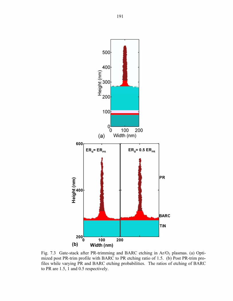
191
Fig. 7.3 Gate-stack after PR-trimming and BARC etching in Ar/O2 plasmas. (a) Opti-mized post PR-trim profile with BARC to PR etching ratio of 1.5. (b) Post PR-trim pro-files while varying PR and BARC etching probabilities. The ratios of etching of BARC to PR are 1.5, 1 and 0.5 respectively.

192
Fig. 7.4 Fluxes to the wafer as a function of radius (Ar/BCl3/Cl2=5/40/55, 300 W ICP, 5 mTorr, 100 sccm). (a) Ion fluxes and (b) neutral fluxes. The scaling for fluxes are indicated in the figure. Cl is the major neutral radical flux and BCl2
+ is the dominant ion.

193
Fig. 7.5 IEADs to the wafer. (a) BCl2
+, (b) Cl+, and (c) Cl2+. Plasma conditions are
Ar/BCl3/Cl2=5/40/55, 300 W ICP, 5 mTorr, 100 sccm and a bias of 18 V.
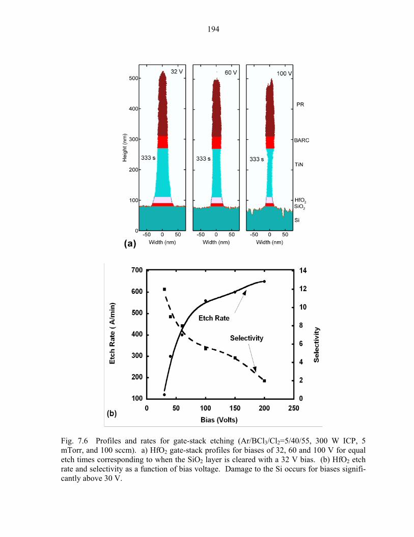
194
Fig. 7.6 Profiles and rates for gate-stack etching (Ar/BCl3/Cl2=5/40/55, 300 W ICP, 5 mTorr, and 100 sccm). a) HfO2 gate-stack profiles for biases of 32, 60 and 100 V for equal etch times corresponding to when the SiO2 layer is cleared with a 32 V bias. (b) HfO2 etch rate and selectivity as a function of bias voltage. Damage to the Si occurs for biases signifi-cantly above 30 V.

195
Fig. 7.7 Post-etch gate-stack profiles for 32, 60 and 100 V. (a) For times when the SiO2 is cleared and (b) optimized profiles with respect to over-etch time.

196
Fig. 7.8 Time sequences for gate-stack profile evolution showing the effect of BARC micro-masking on damage to the Si substrate with low and high bias voltages. (a) With a 32 V bias micro-masking does not cause significant damage to the Si during the over-etch due to the high selectivity. (b) With a 100 V bias the more rapid exposure of Si sites not micro-masked produces damage.

197
Fig. 7.9 Slopes of the gate-stack profile for different bias voltages as a function of over-etch time. A vertical profile corresponds to 900. Higher bias voltages achieve more vertical pro-files with less over-etch but at the cost of selectivity.

198
Fig. 7.10 HfO2/Si selectivity for different bias voltages as a function of the probabilities for (a) Si-B bond formation, (b) polymer deposition, and (c) polymer sputtering. (Ar/BCl3/Cl2=5/40/55, 300 W ICP, 5 mTorr, and 100 sccm).
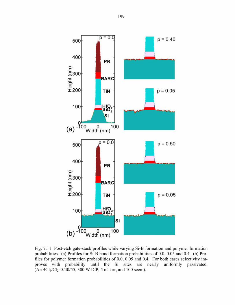
199
Fig. 7.11 Post-etch gate-stack profiles while varying Si-B formation and polymer formation probabilities. (a) Profiles for Si-B bond formation probabilities of 0.0, 0.05 and 0.4. (b) Pro-files for polymer formation probabilities of 0.0, 0.05 and 0.4. For both cases selectivity im-proves with probability until the Si sites are nearly uniformly passivated. (Ar/BCl3/Cl2=5/40/55, 300 W ICP, 5 mTorr, and 100 sccm).
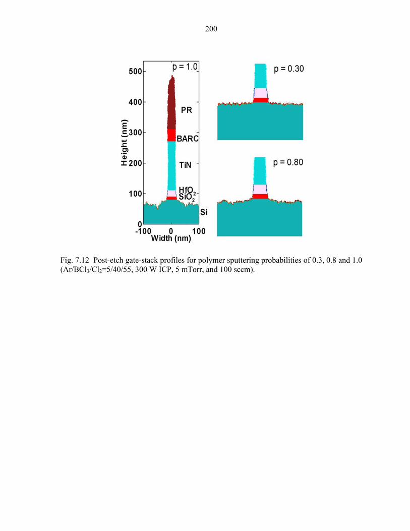
200
Fig. 7.12 Post-etch gate-stack profiles for polymer sputtering probabilities of 0.3, 0.8 and 1.0 (Ar/BCl3/Cl2=5/40/55, 300 W ICP, 5 mTorr, and 100 sccm).

201
7.9 References
1. R. Chau, J. Brask, S. Datta, G. Dewey, M. Doczy, B. Doyle, J. Kavalieros, B. Jin, M.
Metz, A. Majumdar, and M. Radosavljevic, Microelectron. Engr. 80, 1 (2005).
2. B. H. Lee, L. Kang, R. Nieh, W.-J. Qi, and J. C. Lee, Appl. Phys. Lett. 76, 1926 (2000).
3. R. Chau, S. Datta, M. Doczy, B. Doyle, J. Kavalieros, and M. Metz, Elect. Dev. Lett. 25,
408 (2004).
4. O. Joubert , E. Sungauer, E. Pargon, X. Mellhaoui, R. Ramos, G. Cunge and L. Valier ,
J. Vac. Sci. Technol. B 25, 1640 (2007).
5. M. J. Kushner, J. Appl. Phys. 94, 1436 (2003).
6. C. F. Abrams and D. B. Graves, J. Appl. Phys. 86, 2263 (1999).
7. A. Agarwal and M. J. Kushner, J. Vac. Sci. Technol. A 27, 37 (2009).
8. L. Sha, and J. P. Chang, J. Vac. Sci. Technol. A. 21, 1915 (2003).
9. L. Sha, and J. P. Chang, J. Vac. Sci. Technol. A. 22, 88 (2003).
10. M. H. Sin, M. S. Park, and N.–E. Lee, J. Vac. Sci. Technol. A. 24, 1373 (2006).
11. C. Wang and V. M. Donnelly, J. Vac. Sci. Technol. A. 26, 597 (2008).
12. K. Nakamura, D. Hamada, Y. Ueda, K. Eriguchi, and K. Ono, Appl. Phys. Exp. 2,
016503 (2009).
13. L. Sha, R. Puthenkovilakam, Y.-S. Lin, and J. P. Chang, J. Vac. Sci. Technol. B 21,
2420 (2003).
14. M. Hayashi, Technical Report No. IPPJ-AM-19, Nagoya Institute of Technology, 1981.
15. K. Tachibana, Phys. Rev. A 34, 1007 (1986).
16. D. Rapp and P. Englander-Golden J. Chem. Phys. 43, 1464 (1965).
17. R. H. McFarland and J. Kinney, Phys. Rev. A 137, 1058 (1965).
202
18. I. P. Zapesochnyi and L. L. Shimon, Opt. Spectrosc. 11 155 (1966).
19. G. L. Rogoff, J. M. Kramer, and R. B. Piejak, Trans. Plasma Sci. 14, 103 (1986).
20. R. Nagpal and A. Garscadden, Appl. Phys. Lett. 64, 1626 (1994).
21. J. Marriott and J. D. Craggs, J. Electron. Cont. 3, 194 (1957).
22. J. B. A. Mitchell , Phys. Reports 186, 215 (1990).
23. S. G. Lias, J. E. Bartmess, J. F. Liebman, J. L. Holmes, R. D. Levin and W. G. Mallard,
J. Phys. Chem. Ref. Data 17, Supplement 1 (1998).
24. Y. Ikezoe, S. Matsuoka, M. Takabe, and A. Viggiano, Gas Phase Ion-MoleculeReaction
Rate Constants Through 1986 (Mass Spectroscopy Society of Japan, Tokyo, 1987).
25. NIST Chemical Kinetics Database 17, Version 2Q98, http://kinetics.nist.gov/index.php.
26. W. S. Hwang, J. Chen, and W. J. Yoo, J. Vac. Sci. Technol. A 23, 964 (2005).
27. C. -Y. Sin, B. H. Chen, W. L. Loh, J. Yu, P. Yelehanka, A. See, and L.Chan, J. Vac. Sci.
Technol. B 20, 1974 (2002).
28. C. -Y. Sin, B. H. Chen, W. L. Loh, J. Yu, P. Yelehanka, A. See, and L.Chan, AIChE J.
50, 1578 (2004).
29. T. -F. Yen, C. M. Chiu, and K. F. Chiu Microelectron. Engr. 75, 201 (2004).
30. S. Mathew, R. Nagarajan, L. K. Bera, F. H. Hua, D. A. Yan, and N. Balasubramanian,
Thin Solid Films 63, 462 (2004).

203
8. CONCLUSIONS AND FUTURE WORK
8.1 Conclusions
The primary motivation of this thesis is the improved understanding of poorly-known
surface-plasma interaction mechanisms for nano-scale processing. The thesis addresses reac-
tion mechanisms for processes involving low-k dielectrics and high-k gate-stacks, both of
which have been extensively investigated over the last few years. Understanding such mech-
anisms is important for better control and optimization of plasma processes in semiconductor
fabrication. The mechanisms discussed in this thesis have been developed through extensive
parameterization using fragmented data available in literature while reproducing experi-
mental results. The mechanisms can be further refined as more (consistent) experimental re-
sults are made available.
For the processing of low-k porous SiCOH, selection of a plasma mixture for a pro-
cess should depend on its capability to preserve −CH3 groups. This is because −CH3 groups
block water incorporation into the low-k and thus prevent the rise of the k value of the porous
film. For example, in the thesis, we found He/H2 plasmas to be a better option compared to
Ar/O2 for cleaning and PR stripping. For an interconnected porous network, radicals play the
dominant role in the demethylation process through diffusion into the network, which is re-
sponsible for the loss of −CH3 groups and subsequent water uptake and low-k degradation.
However, ions can also increase such damage to some extent near the surface.
We also found that VUV or UV photons with wavelengths <140 nm have the energy
to break Si-C bonds of SiO2-CH3 groups which can then act as an accelerating factor for the
demethylation process. Such bond scission produces the opportunity for radicals and even
for molecules to speed demethylation. The capability of gaining control on the preservation

204
of the low-k can be enhanced by implementing a technique that blocks or seals surface pore-
openings. We have investigated the use of surface-pore sealing with sequential He and NH3
plasmas and predicted closing of surface pores which prevented pathways required by humid
air to diffuse into the network.
For high-k gate-stack etching, the important priority is a high high-k/Si selectivity.
Such selectivity protects the regions of the Si substrate where source and drain of the transis-
tor are located. The prerequisite for such selectivity is to select plasmas that can form a pas-
sivation layer on the Si substrate and to control the substrate bias such that the ion energy is
high enough to etch the high-k material but still below the etching threshold of the pas-
sivation layer formed on the Si substrate. Such a passivation layer can be a compound with
Si-M bonds where M is an element of the plasma, or a polymer deposited on the Si substrate,
or both. It is important to understand the nature and characteristic of such Si-M bonding and
polymers because such compounds will decide if the passivation is able to provide the ex-
pected selectivity under certain bias conditions.
We investigated selective HfO2/Si etching in Ar/Cl2/BCl3 plasmas. We found the
formation of Si-B bonding on Si substrate and BClx polymers on the top of Si-B bonding is
the mechanism responsible for the high HfO2/Si selectivity. If the ion energy is controlled
such that the ion energy is above the threshold of HfO2 etching but lower than the sputtering
threshold of BClx polymers and Si-B bonding, then a high selectivity can be obtained.
8.2 Future Work
In our computational investigation, we simulated the etching of porous SiCOH in flu-
orocarbon plasmas and cleaned deposited CFx polymers after such etching. To realize porous
205
low-k in our model, we substituted pore bordering SiO2 cells with hydrophobic −CH3 groups.
Future modeling can involve realization of more complex organic porous materials where
such −CH3 groups are included beyond the pore border. To investigate pore sealing mecha-
nisms with successive He and NH3 plasma treatment, we considered only chemical interac-
tions between He plasma species and porous low-k surface. These interactions are responsi-
ble for surface activation which prepares the surface for a better sealing in the subsequent
NH3 plasma treatment. However, some experimental results have suggested even more com-
plex mechanisms during the He pretreatment which involve the shrinking of the pore-neck
(surface densification). Along with the chemical modifications such shrinkage facilitates the
pore sealing. Future work can include such pore-neck shrinking mechanisms during He pre-
treatment.
To clean deposited CFx polymer etching formed during fluorocarbon plasma etching
of porous SiCOH and strip masking PR, we investigated both Ar/O2 and He/H2 plasmas.
While He/H2 plasmas produced little damage compared to Ar/O2 plasmas, the PR stripping
rate is much slower. Recently, industry has implemented cleaning methods based on CO or
CO2 plasmas. It has been reported that such cleaning is less harmful to −CH3 groups com-
pared to O2 plasmas but can still strip PR with a faster rate compared to He/H2 plasmas. The
low damage in CO2 cleaning may be attributed to the lower flux of O radicals in a CO2 plas-
ma, which is the dominant agent for cleaning. The O flux in CO/CO2 plasmas is approxi-
mately one fifth that in comparable Ar/O2 plasmas. Also, perhaps, VUV/UV photon fluxes
with wavelengths <140 nm, which are agents for demethylation, are less dominant in CO2
plasmas compared to Ar/O2 plasmas.

206
Our reaction mechanism for gate-stack addressed TiN/HfO2/Si gate-stack etching.
The reaction mechanism can be updated for a more complex high-k such as HfSiON etching
and for etching a different metal gate than TiN. The gate-stack reaction mechanism can also
be modified for a process that uses a different but still Cl2 or BCl3 based plasmas.
207
AUTHOR’S BIOGRAPHY
Juline Shoeb received his BS in Electrical Engineering from Bangladesh University
of Engineering and Technology in 2004. He completed his MS in Electrical Engineering in
2007 from North Dakota State University where his research involved modeling of maximum
power extraction algorithms for solar panels. He joined Iowa State University in 2007 Au-
gust as a PhD student in the group of Prof. Mark J. Kushner and has been working on plas-
ma-surface interactions modeling for nano-scale processing. His PhD research includes
modeling and development of reaction mechanisms and feature-scale profiling that addresses
porous low-k clean, sealing and degradation, and high-k gate-stack etching with Si selectivi-
ty. Under the guidance of Prof. Kushner his work has resulted in 3 published refereed jour-
nal publications with 2 more submitted, 12 conference presentations and 3 conference publi-
cations. Upon graduation in February 2012 with his Ph. D in Electrical Engineering from
Iowa State University, he will work with Lam Research Corp. in Fremont, CA as a process
engineer.
Related Documents