VMIC0001 PLASMA EQUIPMENT MODELING FOR PROCESS DESIGN* Mark J. Kushner University of Illinois Department of Electrical and Computer Engineering Urbana, IL 61801 http://uigelz.ece.uiuc.edu June 2000 *Work supported by: NSF, SRC and DARPA/AFOSR

Welcome message from author
This document is posted to help you gain knowledge. Please leave a comment to let me know what you think about it! Share it to your friends and learn new things together.
Transcript
VMIC0001
PLASMA EQUIPMENT MODELING FORPROCESS DESIGN*
Mark J. KushnerUniversity of Illinois
Department of Electrical and Computer EngineeringUrbana, IL 61801
http://uigelz.ece.uiuc.edu
June 2000
*Work supported by: NSF, SRC and DARPA/AFOSR

AGENDA
VMIC0007
University of Illinois Optical and Discharge Physics
• Goals and requirements for Plasma Equipment and Process Modeling
• A "Walk-Through" of plasma properties for ICP conductor etching.
• Overview of Modeling Hierarchy
• Profile Control for Etching and Deposition
• Concluding Remarks
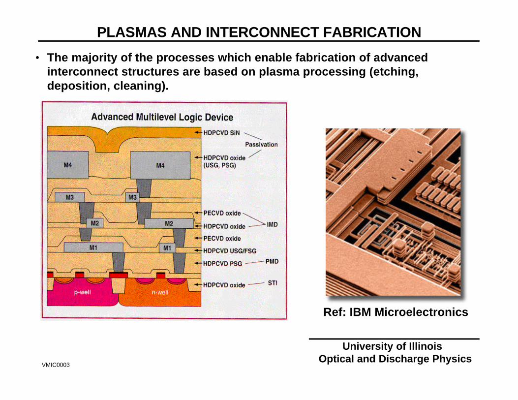
PLASMAS AND INTERCONNECT FABRICATION
VMIC0003
University of Illinois Optical and Discharge Physics
• The majority of the processes which enable fabrication of advancedinterconnect structures are based on plasma processing (etching,deposition, cleaning).
Ref: IBM Microelectronics
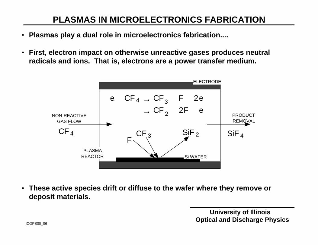
PLASMAS IN MICROELECTRONICS FABRICATION
ICOPS00_06
University of Illinois Optical and Discharge Physics
• Plasmas play a dual role in microelectronics fabrication....
• First, electron impact on otherwise unreactive gases produces neutralradicals and ions. That is, electrons are a power transfer medium.
ELECTRODE
PLASMA REACTOR
NON-REACTIVE GAS FLOW
PRODUCT REMOVAL
e + CF 4 → CF3+ + F + 2e
→ CF 2 + 2F + e
Si WAFER
CF 3+
FSiF 2CF 4 SiF 4
• These active species drift or diffuse to the wafer where they remove ordeposit materials.
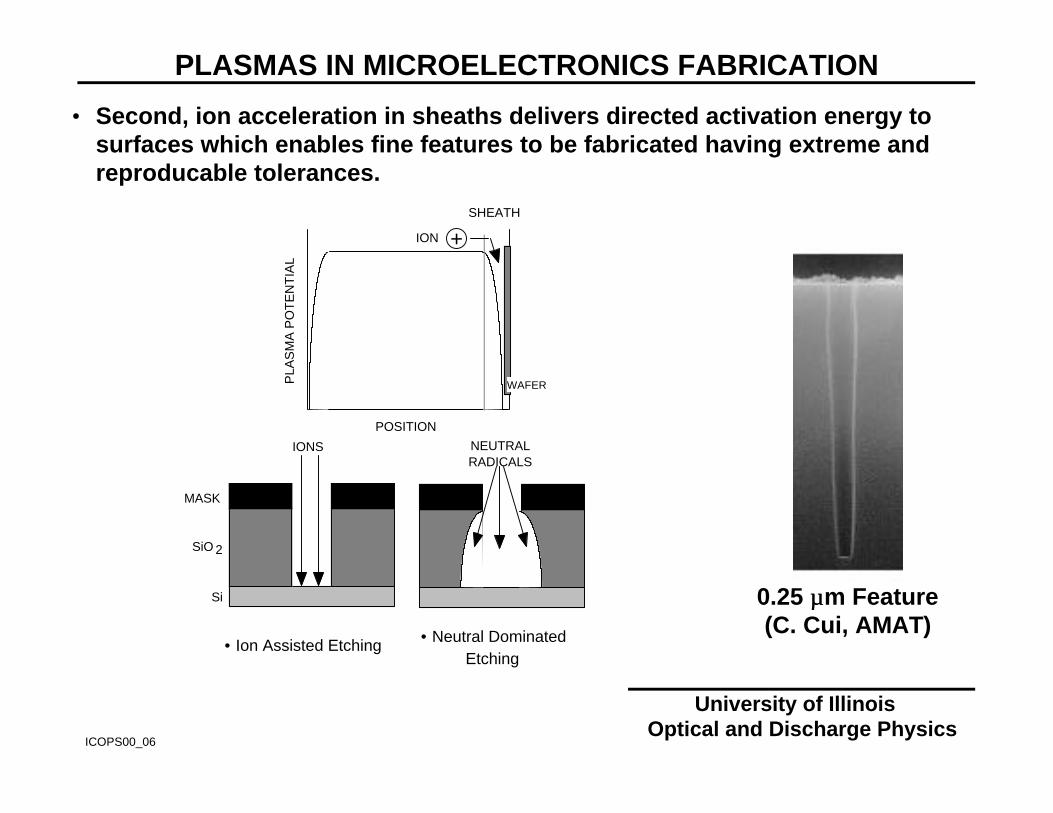
PLASMAS IN MICROELECTRONICS FABRICATION
ICOPS00_06
University of Illinois Optical and Discharge Physics
• Second, ion acceleration in sheaths delivers directed activation energy tosurfaces which enables fine features to be fabricated having extreme andreproducable tolerances.
PLA
SM
A P
OT
EN
TIA
L
POSITION
WAFER
SHEATH
+ION
IONS
MASK
SiO 2
Si
• Ion Assisted Etching • Neutral Dominated Etching
NEUTRAL RADICALS
0.25 µµm Feature(C. Cui, AMAT)
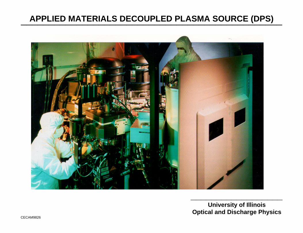
APPLIED MATERIALS DECOUPLED PLASMA SOURCE (DPS)_______________________________________________
__________________University of Illinois
Optical and Discharge PhysicsCECAM9826
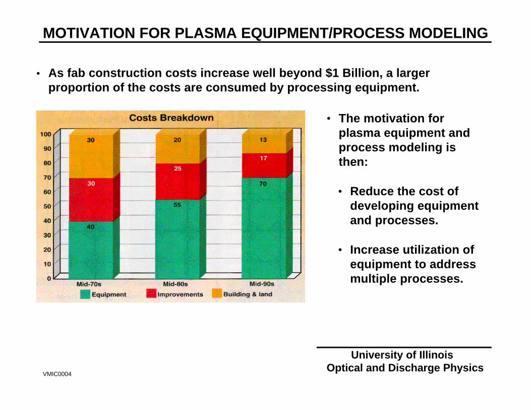
MOTIVATION FOR PLASMA EQUIPMENT/PROCESS MODELING
VMIC0004
University of Illinois Optical and Discharge Physics
•• As fab construction costs increase well beyond $1 Billion, a largerproportion of the costs are consumed by processing equipment.
• The motivation forplasma equipment andprocess modeling isthen:
• Reduce the cost ofdeveloping equipmentand processes.
• Increase utilization ofequipment to addressmultiple processes.
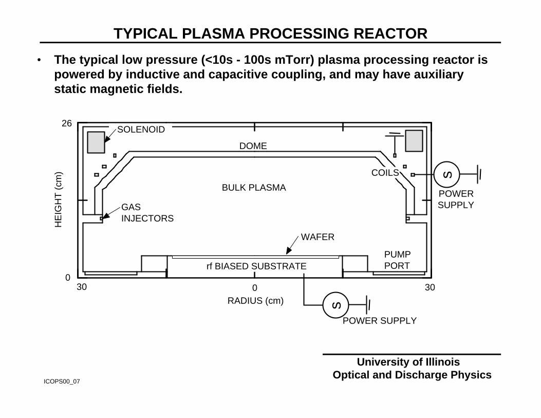
TYPICAL PLASMA PROCESSING REACTOR
ICOPS00_07
University of Illinois Optical and Discharge Physics
• The typical low pressure (<10s - 100s mTorr) plasma processing reactor ispowered by inductive and capacitive coupling, and may have auxiliarystatic magnetic fields.
PUMP PORT
DOME
GAS INJECTORS
BULK PLASMA
WAFER
30 30 0
RADIUS (cm)
HE
IGH
T (
cm)
0
26
sCOILS
s
rf BIASED SUBSTRATE
SOLENOID
POWER SUPPLY
POWER SUPPLY
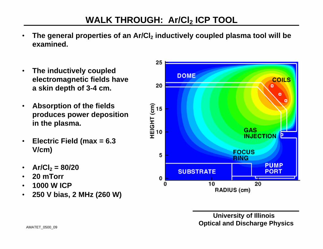
WALK THROUGH: Ar/Cl2 ICP TOOL
AMATET_0500_09
University of Illinois Optical and Discharge Physics
• The general properties of an Ar/Cl2 inductively coupled plasma tool will beexamined.
• The inductively coupledelectromagnetic fields havea skin depth of 3-4 cm.
• Absorption of the fieldsproduces power depositionin the plasma.
• Electric Field (max = 6.3V/cm)
• Ar/Cl2 = 80/20• 20 mTorr• 1000 W ICP• 250 V bias, 2 MHz (260 W)
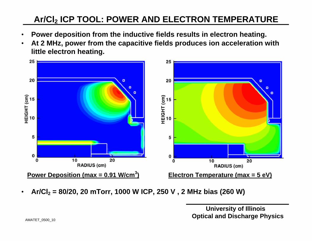
Ar/Cl2 ICP TOOL: POWER AND ELECTRON TEMPERATURE
AMATET_0500_10
University of Illinois Optical and Discharge Physics
• Power deposition from the inductive fields results in electron heating.• At 2 MHz, power from the capacitive fields produces ion acceleration with
little electron heating.
Power Deposition (max = 0.91 W/cm3) Electron Temperature (max = 5 eV)
• Ar/Cl2 = 80/20, 20 mTorr, 1000 W ICP, 250 V , 2 MHz bias (260 W)
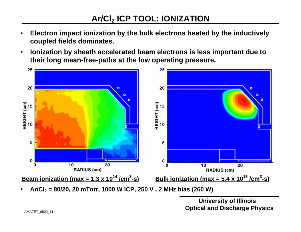
Ar/Cl2 ICP TOOL: IONIZATION
AMATET_0500_11
University of Illinois Optical and Discharge Physics
• Electron impact ionization by the bulk electrons heated by the inductivelycoupled fields dominates.
• Ionization by sheath accelerated beam electrons is less important due totheir long mean-free-paths at the low operating pressure.
Beam ionization (max = 1.3 x 10¹⁴ /cm3-s) Bulk ionization (max = 5.4 x 10¹⁵ /cm3-s)
• Ar/Cl2 = 80/20, 20 mTorr, 1000 W ICP, 250 V , 2 MHz bias (260 W)
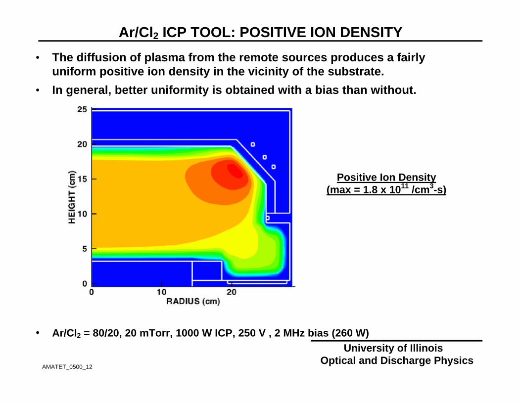
Ar/Cl2 ICP TOOL: POSITIVE ION DENSITY
AMATET_0500_12
University of Illinois Optical and Discharge Physics
• The diffusion of plasma from the remote sources produces a fairlyuniform positive ion density in the vicinity of the substrate.
• In general, better uniformity is obtained with a bias than without.
Positive Ion Density(max = 1.8 x 10¹¹ /cm3-s)
• Ar/Cl2 = 80/20, 20 mTorr, 1000 W ICP, 250 V , 2 MHz bias (260 W)

Ar/Cl2 ICP TOOL: BIAS CURRENTS, POTENTIALS
ICOPS00_14
University of Illinois Optical and Discharge Physics
2 MHz SUBSTRATE
PO
TE
NT
IAL
(V
)
• The small currentcollection area of thesubstract produces alarge negative dc bias
• The large sheathpotential results inelectron current beingcollected during a smallfraction of the rf cycle.
• The non-linearity of thesheaths at differentsurfaces also contributesto the non-sinusoidalcurrent.
• Ar/Cl2 = 80/20, 20 mTorr,1000 W ICP, 250 V , 2 MHzbias (260 W)
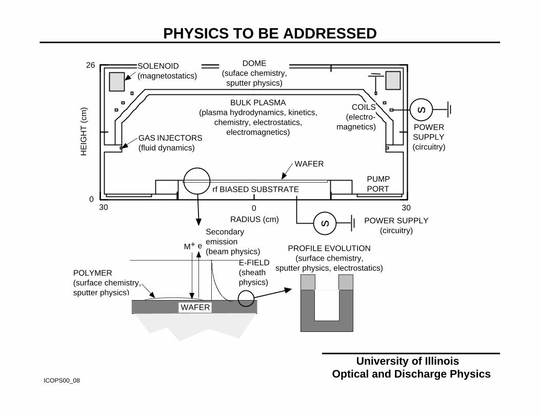
PHYSICS TO BE ADDRESSED
ICOPS00_08
University of Illinois Optical and Discharge Physics
PUMP PORT
GAS INJECTORS (fluid dynamics)
BULK PLASMA (plasma hydrodynamics, kinetics,
chemistry, electrostatics,electromagnetics)
WAFER
30 30 0
RADIUS (cm)
HE
IGH
T (
cm)
0
26
sCOILS (electro-
magnetics)
s
rf BIASED SUBSTRATE
SOLENOID (magnetostatics)
DOME (suface chemistry, sputter physics)
POWER SUPPLY (circuitry)
POWER SUPPLY (circuitry)
POLYMER (surface chemistry, sputter physics)
M+ e
Secondary emission (beam physics)
WAFER
E-FIELD (sheath physics)
PROFILE EVOLUTION (surface chemistry,
sputter physics, electrostatics)
UNIVERSITY OF ILLINOISOPTICAL AND DISCHARGE PHYSICS
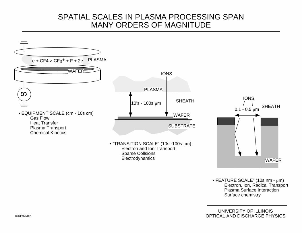
SPATIAL SCALES IN PLASMA PROCESSING SPANMANY ORDERS OF MAGNITUDE
ICRP97M12
• EQUIPMENT SCALE (cm - 10s cm)Gas FlowHeat TransferPlasma TransportChemical Kinetics
PLASMA
WAFER
e + CF4 > CF3+ + F + 2e
• FEATURE SCALE” (10s nm - µm)Electron, Ion, Radical TransportPlasma Surface InteractionSurface chemistry
IONS
SHEATH0.1 - 0.5 µm
WAFER
• “TRANSITION SCALE” (10s -100s µm)Electron and Ion TransportSparse CollsionsElectrodynamics
WAFER
SHEATH
SUBSTRATE
10’s - 100s µm
IONS
PLASMA
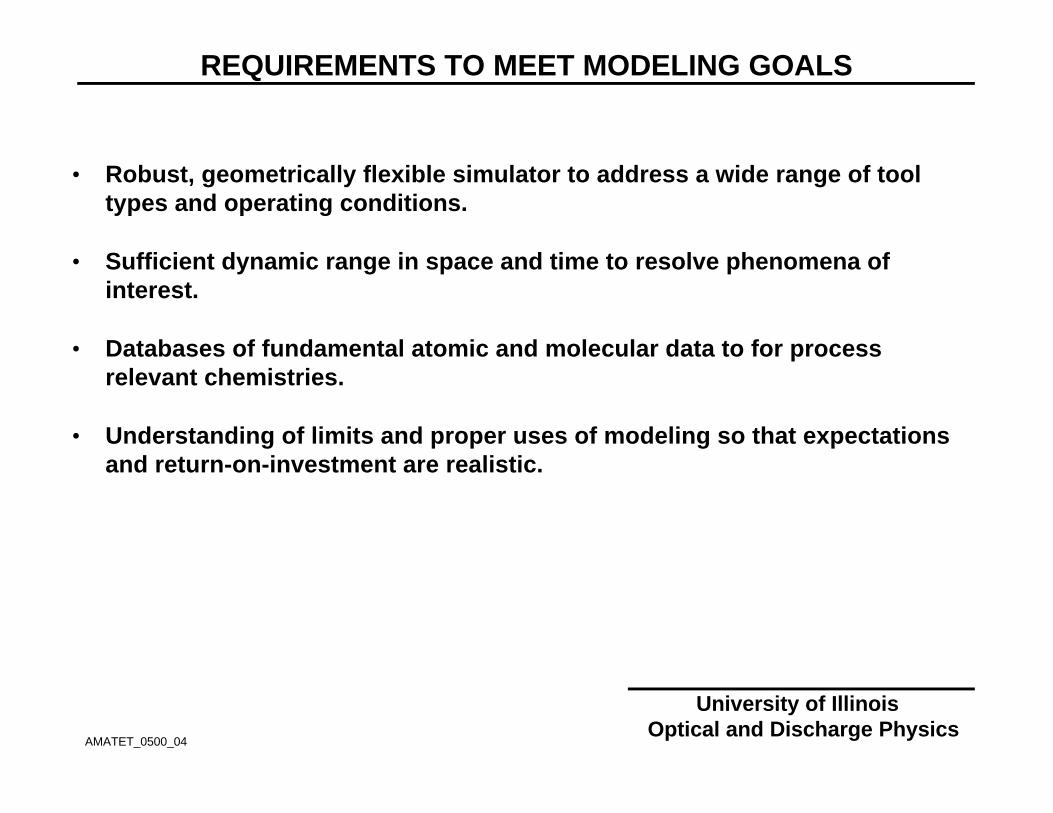
REQUIREMENTS TO MEET MODELING GOALS
AMATET_0500_04
University of Illinois Optical and Discharge Physics
• Robust, geometrically flexible simulator to address a wide range of tooltypes and operating conditions.
• Sufficient dynamic range in space and time to resolve phenomena ofinterest.
• Databases of fundamental atomic and molecular data to for processrelevant chemistries.
• Understanding of limits and proper uses of modeling so that expectationsand return-on-investment are realistic.
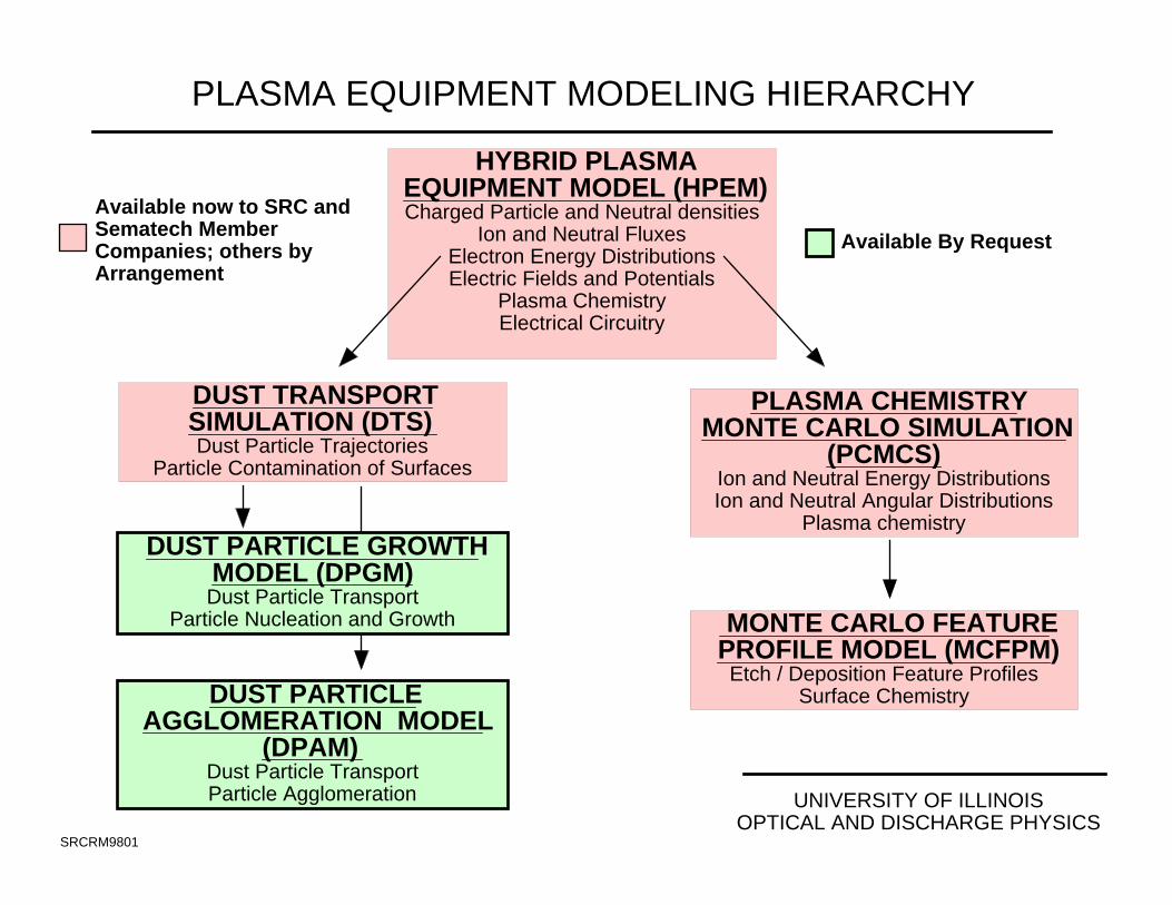
PLASMA EQUIPMENT MODELING HIERARCHY
UNIVERSITY OF ILLINOISOPTICAL AND DISCHARGE PHYSICS
SRCRM9801
HYBRID PLASMAEQUIPMENT MODEL (HPEM)Charged Particle and Neutral densities
Ion and Neutral FluxesElectron Energy DistributionsElectric Fields and Potentials
Plasma ChemistryElectrical Circuitry
PLASMA CHEMISTRYMONTE CARLO SIMULATION
(PCMCS)Ion and Neutral Energy DistributionsIon and Neutral Angular Distributions
Plasma chemistry
MONTE CARLO FEATUREPROFILE MODEL (MCFPM)
Etch / Deposition Feature ProfilesSurface Chemistry
DUST TRANSPORTSIMULATION (DTS)Dust Particle Trajectories
Particle Contamination of Surfaces
DUST PARTICLEAGGLOMERATION MODEL
(DPAM)Dust Particle TransportParticle Agglomeration
DUST PARTICLE GROWTHMODEL (DPGM)Dust Particle Transport
Particle Nucleation and Growth
Available now to SRC andSematech MemberCompanies; others byArrangement
Available By Request
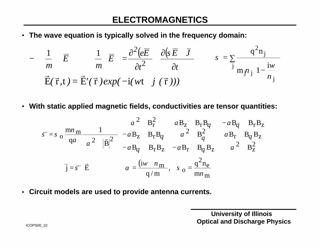
ELECTROMAGNETICS
ICOPS00_10
University of Illinois Optical and Discharge Physics
• The wave equation is typically solved in the frequency domain:
( ) ( )t
JE
t
E E E
2
∂
+∂+
∂
∂=
∇⋅∇+
⋅∇∇−
σεµµ 211
r r r r rE r t E r i t r( , ) ( )exp( ( ( )))= ′ − +ω ϕ
σ
νω
ν
=
−
∑q n
mi
j
j jj
j
2
1
• With static applied magnetic fields, conductivities are tensor quantities:
( )m
e2
om
2z
2zrzr
zr22
rz
zrrz2r
2
22m
o
m
nq,
m/qi
Ej
BBBBBBB
BBBBBBB
BBBBBBB
B
1
q
m
νσ
νωασ
ααα
ααα
ααα
ααν
σσ
θθ
θθθ
θθ
=+
=⋅=
++−+−
+++−
+−++
+
=
r&&&
v
r&&&
•• Circuit models are used to provide antenna currents.
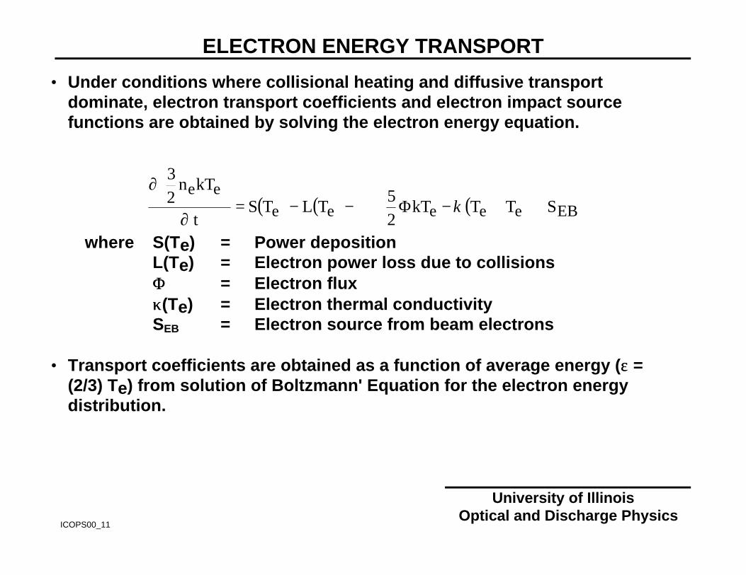
ELECTRON ENERGY TRANSPORT
ICOPS00_11
University of Illinois Optical and Discharge Physics
• Under conditions where collisional heating and diffusive transportdominate, electron transport coefficients and electron impact sourcefunctions are obtained by solving the electron energy equation.
( ) ( ) ( ) EBeeeeeee
STTkT25
TLTSt
kTn23
+
∇−Φ⋅∇−−=
∂
∂
κ
where S(Te) = Power depositionL(Te) = Electron power loss due to collisionsΦΦ = Electron fluxκκ(Te) = Electron thermal conductivitySEB = Electron source from beam electrons
• Transport coefficients are obtained as a function of average energy (εε =(2/3) Te) from solution of Boltzmann' Equation for the electron energydistribution.
ELECTRON ENERGY TRANSPORT
ICOPS00_11
University of Illinois Optical and Discharge Physics
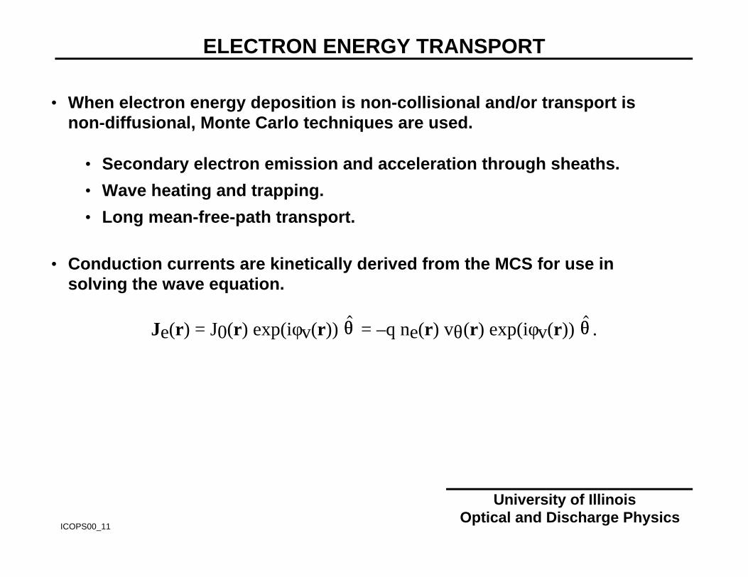
• When electron energy deposition is non-collisional and/or transport isnon-diffusional, Monte Carlo techniques are used.
• Secondary electron emission and acceleration through sheaths.
• Wave heating and trapping.
• Long mean-free-path transport.
• Conduction currents are kinetically derived from the MCS for use insolving the wave equation.
Je(r) = J0(r) exp(iφv(r)) $θθ = –q ne(r) vθ(r) exp(iφv(r)) $θθ .

PLASMA CHEMISTRY, TRANSPORT AND ELECTROSTATICS
ICOPS00_12
University of Illinois Optical and Discharge Physics
• Multi-fluid techniques are used where continuity, momentum and energyequations are solved for each species, with coupling terms for exchangeof momentum and energy.
iiii S)vN(
t
N+⋅−∇= r
∂∂
( ) ( ) ( ) ( ) iii
iiiiiii
i
ii BvEm
NqvvNTkN
m
1
t
vNµ
∂∂
⋅∇−×++⋅∇−∇=rrrrr
r
( ) ijjijj
ijmim
jvvNN
mνrr −∑−
+
( ) 222
ii
i2ii
iiiiiiii E
)(m
qN)UN(UPQ
tN
ων
νε
∂ε∂
+=⋅∇+⋅∇+⋅∇+
∑±∑ −+
++j
jBijjij
ijBijjiji
ij2s
ii
2ii
TkRNN3)TT(kRNNmm
m3E
m
qN
ν ,
•• Slip boundary conditions are used for neutral transport for momentum andenergy to address momentum and temperature jump conditions.
PLASMA CHEMISTRY, TRANSPORT AND ELECTROSTATICS
ICOPS00_12
University of Illinois Optical and Discharge Physics
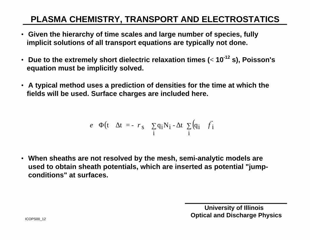
• Given the hierarchy of time scales and large number of species, fullyimplicit solutions of all transport equations are typically not done.
• Due to the extremely short dielectric relaxation times (<< 10-12 s), Poisson'sequation must be implicitly solved.
• A typical method uses a prediction of densities for the time at which thefields will be used. Surface charges are included here.
( ) ( )
∑ ⋅∇⋅∆∑+=∆+Φ∇⋅∇i
iii
iis qt-Nq-tt φρεr
• When sheaths are not resolved by the mesh, semi-analytic models areused to obtain sheath potentials, which are inserted as potential "jump-conditions" at surfaces.
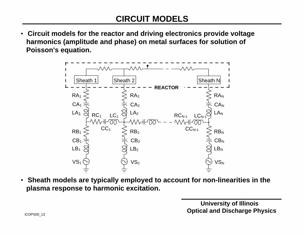
CIRCUIT MODELS
ICOPS00_13
University of Illinois Optical and Discharge Physics
• Circuit models for the reactor and driving electronics provide voltageharmonics (amplitude and phase) on metal surfaces for solution ofPoisson's equation.
Sheath 1 Sheath 2 Sheath N
RC1
CC1
LC1
RB1
CB1
VS1
LB1
RA1
CA1
LA1
RB2
CB2
VS2
LB2
RA2
CA2
LA2
RBN
CBN
VSN
LBN
RAN
CAN
LANRCN-1
CCN-1
LCN-1
REACTOR
• Sheath models are typically employed to account for non-linearities in theplasma response to harmonic excitation.
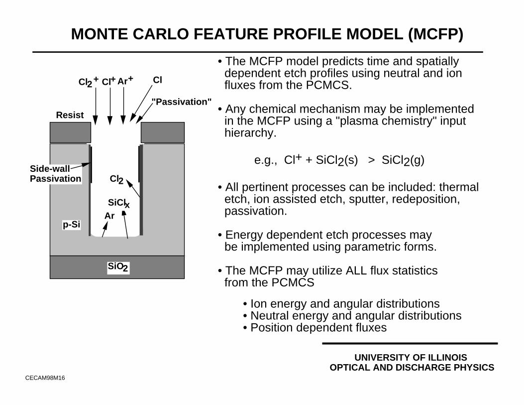
• The MCFP model predicts time and spatially dependent etch profiles using neutral and ion fluxes from the PCMCS.
• Any chemical mechanism may be implemented in the MCFP using a "plasma chemistry" input hierarchy.
e.g., Cl+ + SiCl2(s) > SiCl2(g)
• All pertinent processes can be included: thermal etch, ion assisted etch, sputter, redeposition, passivation.
• Energy dependent etch processes may be implemented using parametric forms.
• The MCFP may utilize ALL flux statistics from the PCMCS
• Ion energy and angular distributions• Neutral energy and angular distributions• Position dependent fluxes
MONTE CARLO FEATURE PROFILE MODEL (MCFP)
Resist
p-Si
SiO2
Cl
Ar
Cl2
Cl+
UNIVERSITY OF ILLINOISOPTICAL AND DISCHARGE PHYSICS
CECAM98M16
SiClx
"Passivation"
Side-wallPassivation
Ar+Cl2+
PROFILE CONTROL FOR INTERCONNECT: ETCH AND DEP
VMIC0006
University of Illinois Optical and Discharge Physics
FLUOROCARBON ETCHING OF DIELECTRICS
IONIZED METAL PVD OF COPPER
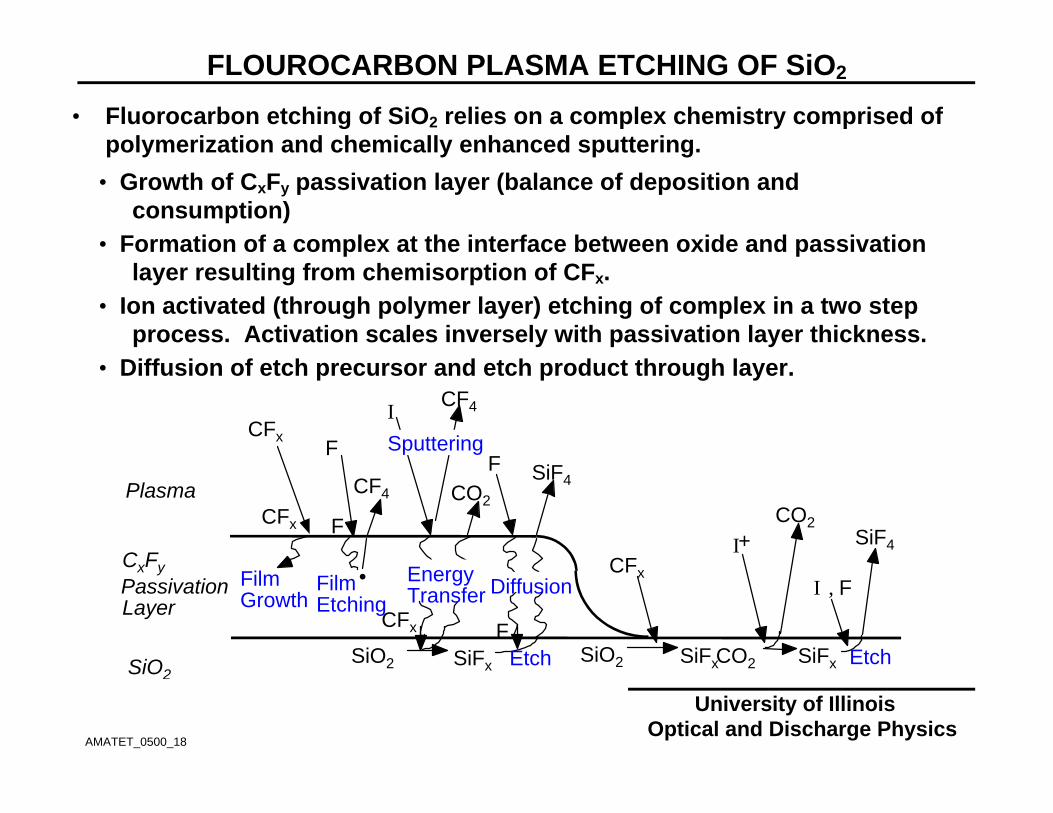
FLOUROCARBON PLASMA ETCHING OF SiO2
AMATET_0500_18
University of Illinois Optical and Discharge Physics
• Fluorocarbon etching of SiO2 relies on a complex chemistry comprised ofpolymerization and chemically enhanced sputtering.
• Growth of CxFy passivation layer (balance of deposition andconsumption)
• Formation of a complex at the interface between oxide and passivationlayer resulting from chemisorption of CFx.
• Ion activated (through polymer layer) etching of complex in a two stepprocess. Activation scales inversely with passivation layer thickness.
• Diffusion of etch precursor and etch product through layer.
CFx
SiO2 SiFx
F
CF4
F
SiF4
Film Growth
•Film Etching
F
Etch
DiffusionCxFy
Passivation Layer
Ι+
CFx
CO2
SiO2 SiFxCO2 SiFx
CFx
Ι+CO2
Ι+, FEnergyTransfer
Etch
Plasma
SiO2
CF4
SiF4
F
CFx
Sputtering
UNIVERSITY OF ILLINOISOPTICAL AND DISCHARGE PHYSICS
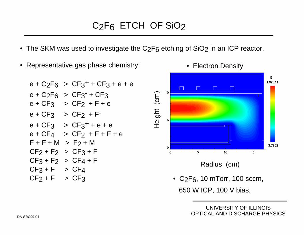
C2F6 ETCH OF SiO2
DA-SRC99-04
• The SKM was used to investigate the C2F6 etching of SiO2 in an ICP reactor.
Radius (cm)
• C2F6, 10 mTorr, 100 sccm,
650 W ICP, 100 V bias.
• Electron Density • Representative gas phase chemistry:
e + C2F6 > CF3+ + CF3 + e + e
e + C2F6 > CF3- + CF3e + CF3 > CF2 + F + e
e + CF3 > CF2 + F-
e + CF3 > CF3+ + e + ee + CF4 > CF2 + F + F + eF + F + M > F2 + MCF2 + F2 > CF3 + FCF3 + F2 > CF4 + FCF3 + F > CF4 CF2 + F > CF3
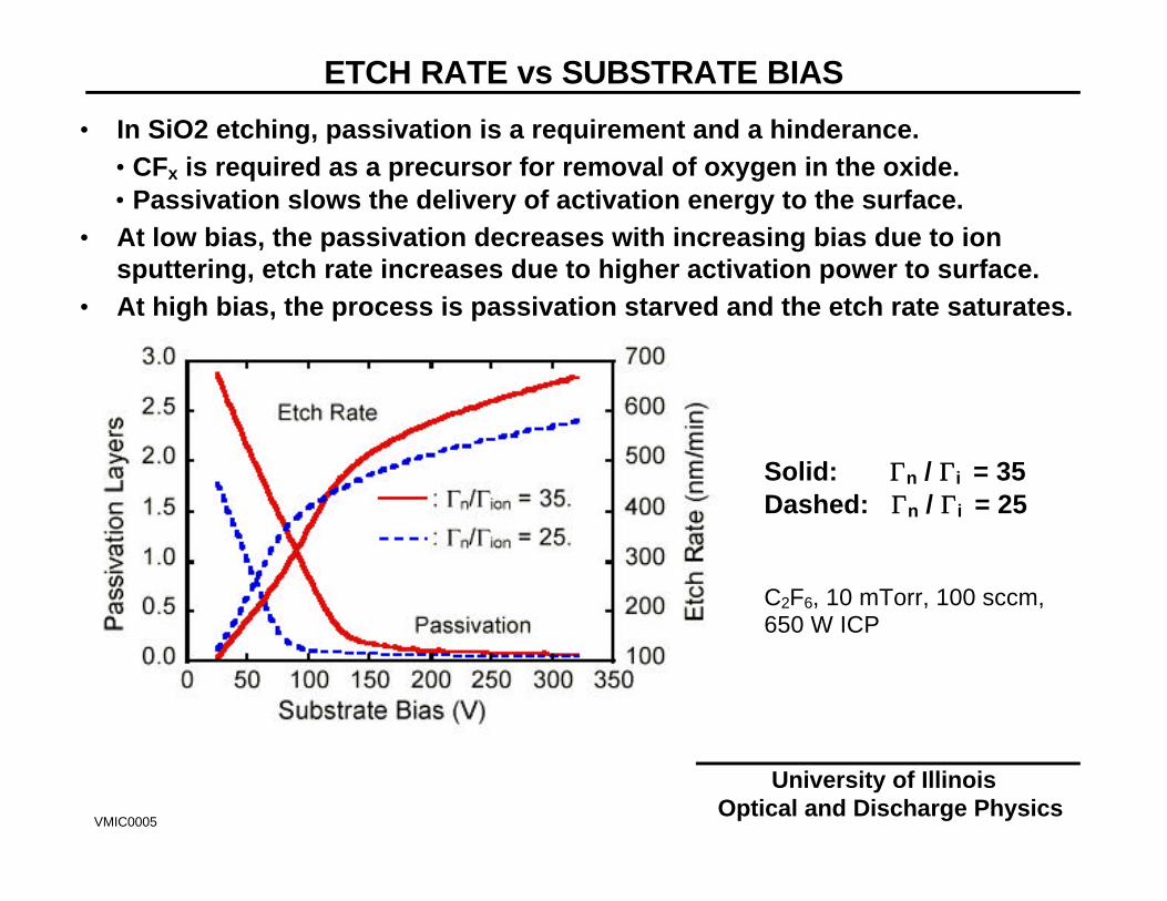
ETCH RATE vs SUBSTRATE BIAS
VMIC0005
University of Illinois Optical and Discharge Physics
• In SiO2 etching, passivation is a requirement and a hinderance.• CFx is required as a precursor for removal of oxygen in the oxide.• Passivation slows the delivery of activation energy to the surface.
• At low bias, the passivation decreases with increasing bias due to ionsputtering, etch rate increases due to higher activation power to surface.
• At high bias, the process is passivation starved and the etch rate saturates.
Solid: ΓΓn / ΓΓi = 35Dashed: ΓΓn / ΓΓi = 25
C2F6, 10 mTorr, 100 sccm,650 W ICP
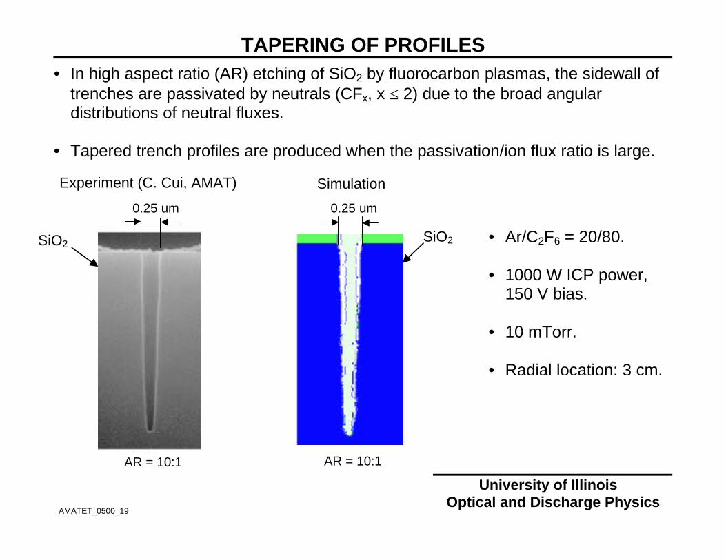
TAPERING OF PROFILES
AMATET_0500_19
University of Illinois Optical and Discharge Physics
• In high aspect ratio (AR) etching of SiO2 by fluorocarbon plasmas, the sidewall oftrenches are passivated by neutrals (CFx, x ≤ 2) due to the broad angulardistributions of neutral fluxes.
• Tapered trench profiles are produced when the passivation/ion flux ratio is large.
8
• Ar/C2F6 = 20/80.
• 1000 W ICP power,150 V bias.
• 10 mTorr.
• Radial location: 3 cm.
Experiment (C. Cui, AMAT) Simulation
0.25 um0.25 um
AR = 10:1 AR = 10:1
SiO2SiO2
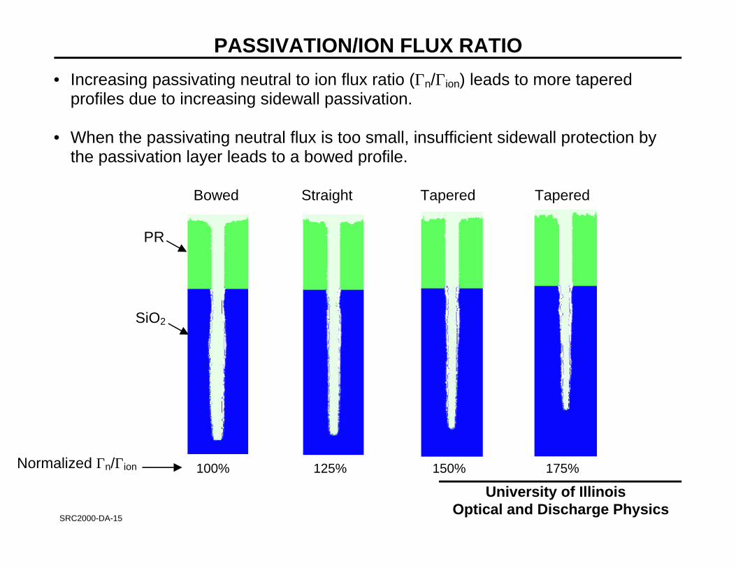
PASSIVATION/ION FLUX RATIO
SRC2000-DA-15
University of Illinois Optical and Discharge Physics
• Increasing passivating neutral to ion flux ratio (Γn/Γion) leads to more taperedprofiles due to increasing sidewall passivation.
• When the passivating neutral flux is too small, insufficient sidewall protection bythe passivation layer leads to a bowed profile.
100% 125% 150% 175%
Bowed Straight Tapered Tapered
Normalized Γn/Γion
PR
SiO2
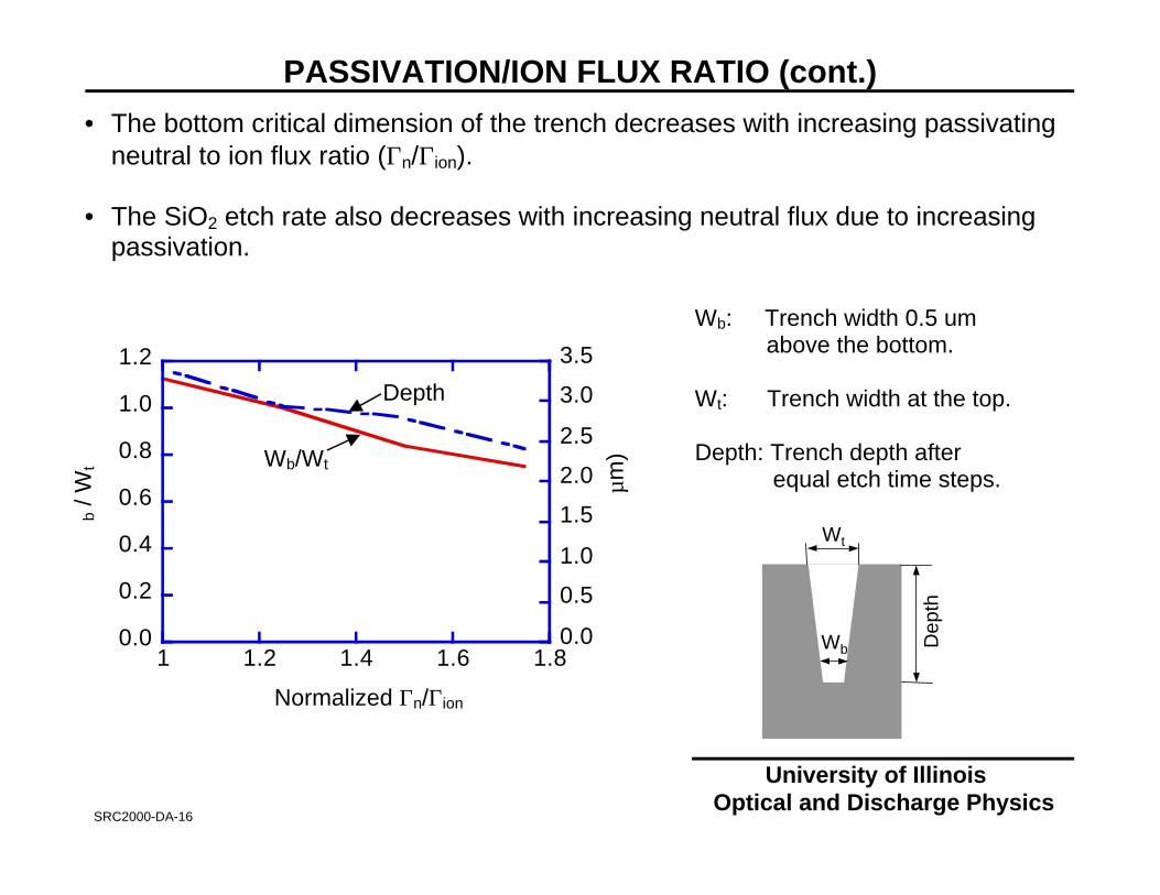
PASSIVATION/ION FLUX RATIO (cont.)
SRC2000-DA-16
University of Illinois Optical and Discharge Physics
• The bottom critical dimension of the trench decreases with increasing passivatingneutral to ion flux ratio (Γn/Γion).
• The SiO2 etch rate also decreases with increasing neutral flux due to increasingpassivation.
Normalized Γn/Γion
0.0
0.2
0.4
0.6
0.8
1.0
1.2
0.0
0.5
1.0
1.5
2.0
2.5
3.0
3.5
1 1.2 1.4 1.6 1.8
b / W
t
µm)
Wb: Trench width 0.5 um above the bottom.
Wt: Trench width at the top.
Depth: Trench depth after equal etch time steps.
Depth
Wb/Wt
Wt
De
pth
Wb
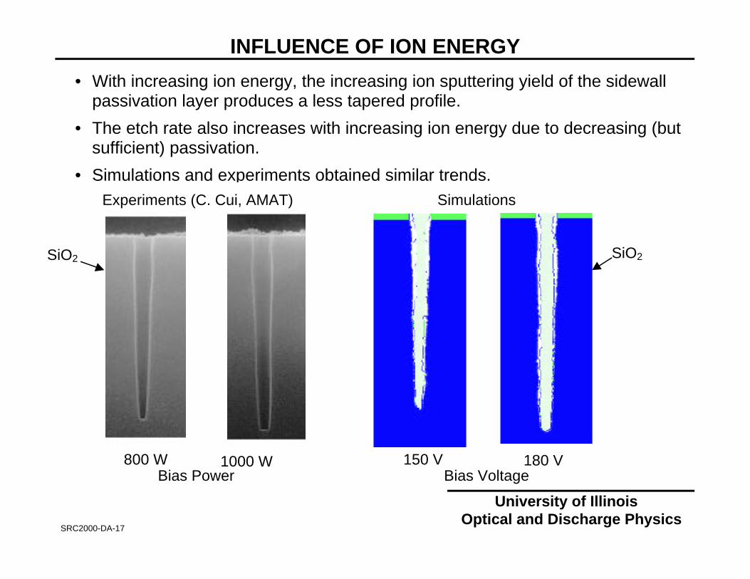
INFLUENCE OF ION ENERGY
SRC2000-DA-17
University of Illinois Optical and Discharge Physics
• With increasing ion energy, the increasing ion sputtering yield of the sidewallpassivation layer produces a less tapered profile.
• The etch rate also increases with increasing ion energy due to decreasing (butsufficient) passivation.
• Simulations and experiments obtained similar trends.
Experiments (C. Cui, AMAT) Simulations
800 W 1000 W 150 V 180 VBias Power
SiO2 SiO2
Bias Voltage
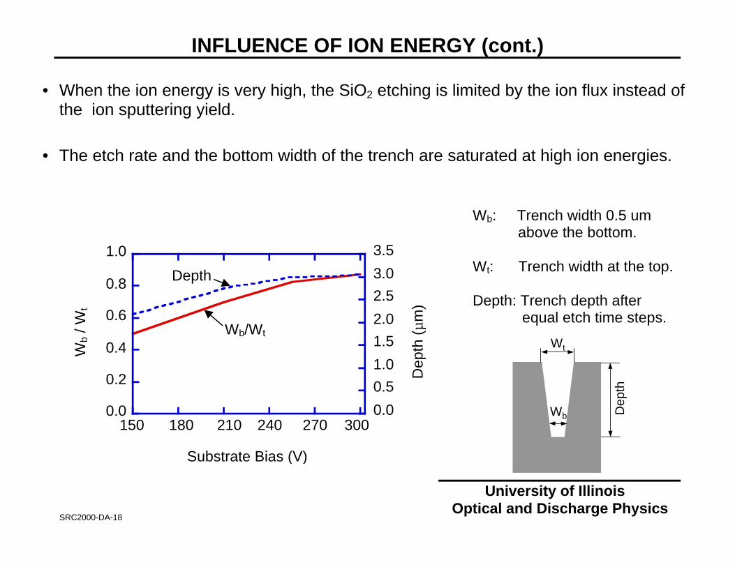
INFLUENCE OF ION ENERGY (cont.)
SRC2000-DA-18
University of Illinois Optical and Discharge Physics
• When the ion energy is very high, the SiO2 etching is limited by the ion flux instead ofthe ion sputtering yield.
• The etch rate and the bottom width of the trench are saturated at high ion energies.
Wb: Trench width 0.5 um above the bottom.
Wt: Trench width at the top.
Depth: Trench depth after equal etch time steps.
Wb/Wt
Depth
Wb / W
t
Depth
(µm
)
Wt
De
pth
Wb0.0
0.2
0.4
0.6
0.8
1.0
0.0
0.5
1.0
1.5
2.0
2.5
3.0
3.5
1.0 1.2 1.4 1.6 1.8 2.0150 300270240210180
Substrate Bias (V)
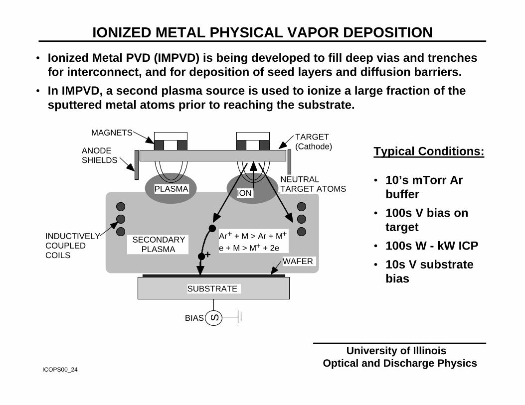
IONIZED METAL PHYSICAL VAPOR DEPOSITION
ICOPS00_24
University of Illinois Optical and Discharge Physics
• Ionized Metal PVD (IMPVD) is being developed to fill deep vias and trenchesfor interconnect, and for deposition of seed layers and diffusion barriers.
• In IMPVD, a second plasma source is used to ionize a large fraction of thesputtered metal atoms prior to reaching the substrate.
TARGET (Cathode)
MAGNETS
ANODE SHIELDS
PLASMA ION
WAFER
INDUCTIVELY COUPLED COILS
SUBSTRATE
S
SECONDARY PLASMA
BIAS
Ar+ + M > Ar + M+
e + M > M+ + 2e
NEUTRAL TARGET ATOMS
+
Typical Conditions:
• 10’s mTorr Arbuffer
• 100s V bias ontarget
• 100s W - kW ICP
• 10s V substratebias
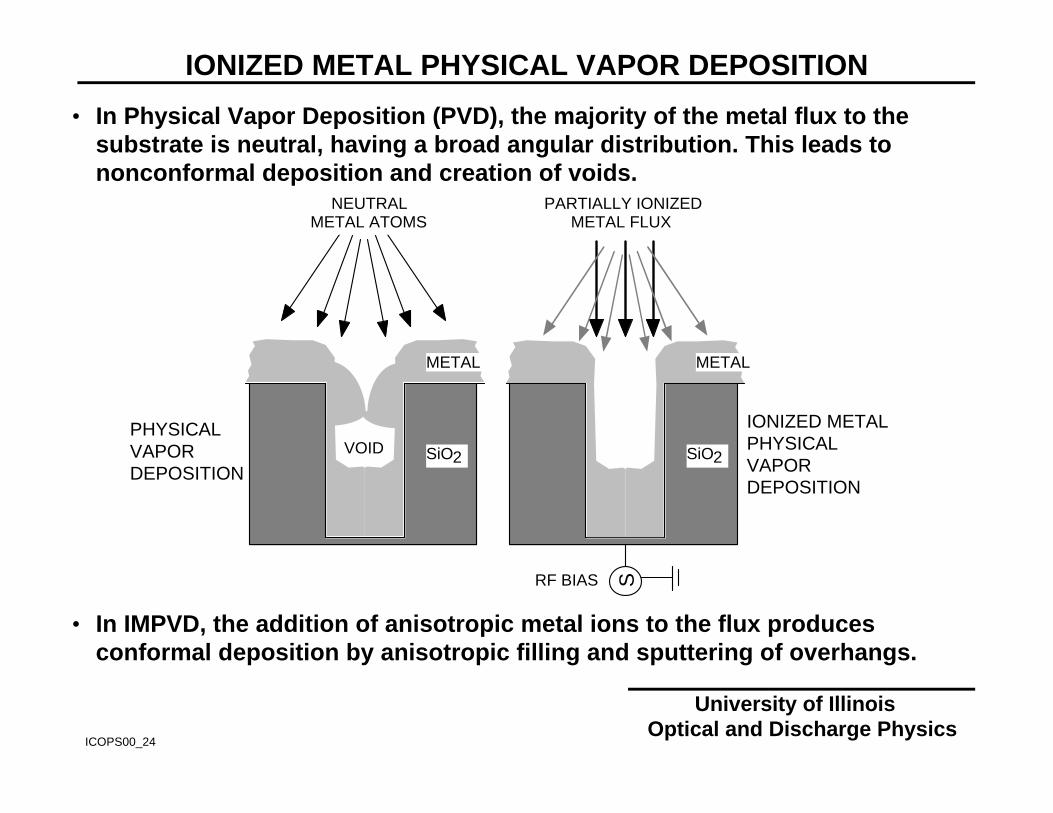
IONIZED METAL PHYSICAL VAPOR DEPOSITION
ICOPS00_24
University of Illinois Optical and Discharge Physics
• In Physical Vapor Deposition (PVD), the majority of the metal flux to thesubstrate is neutral, having a broad angular distribution. This leads tononconformal deposition and creation of voids.
NEUTRALMETAL ATOMS
SiO2
METAL
VOID
PARTIALLY IONIZEDMETAL FLUX
SiO2
METAL
SRF BIAS
PHYSICAL VAPOR DEPOSITION
IONIZED METAL PHYSICAL VAPOR DEPOSITION
• In IMPVD, the addition of anisotropic metal ions to the flux producesconformal deposition by anisotropic filling and sputtering of overhangs.
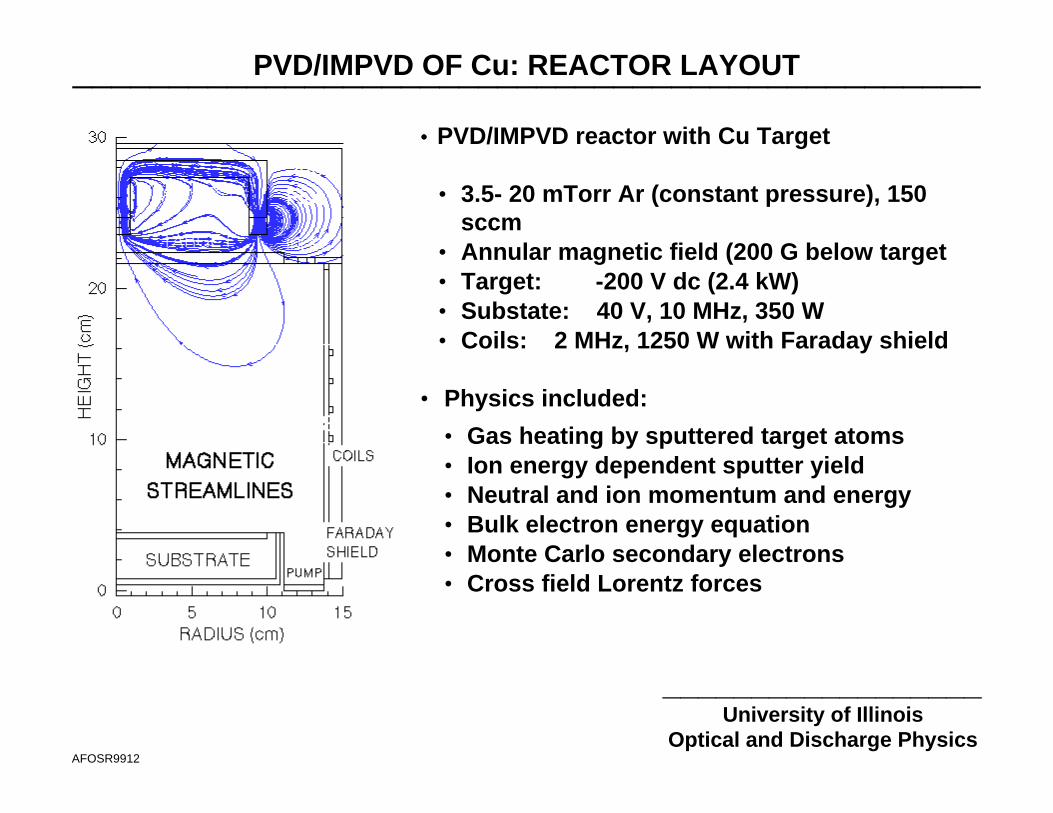
PVD/IMPVD OF Cu: REACTOR LAYOUT_______________________________________________
__________________University of Illinois
Optical and Discharge PhysicsAFOSR9912
•• PVD/IMPVD reactor with Cu Target
• 3.5- 20 mTorr Ar (constant pressure), 150sccm
• Annular magnetic field (200 G below target• Target: -200 V dc (2.4 kW)• Substate: 40 V, 10 MHz, 350 W• Coils: 2 MHz, 1250 W with Faraday shield
• Physics included:
• Gas heating by sputtered target atoms• Ion energy dependent sputter yield• Neutral and ion momentum and energy• Bulk electron energy equation• Monte Carlo secondary electrons• Cross field Lorentz forces
UNIVERSITY OF ILLINOISOPTICAL AND DISCHARGE PHYSICS
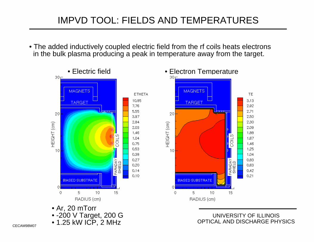
IMPVD TOOL: FIELDS AND TEMPERATURES
CECAM98M07
• Ar, 20 mTorr• -200 V Target, 200 G• 1.25 kW ICP, 2 MHz
• The added inductively coupled electric field from the rf coils heats electrons in the bulk plasma producing a peak in temperature away from the target.
• Electron Temperature• Electric field

UNIVERSITY OF ILLINOISOPTICAL AND DISCHARGE PHYSICS
IMPVD TOOL: ELECTRON SOURCE AND DENSITY
CECAM98M08
• Ar, 20 mTorr• -200 V Target, 200 G• 1.25 kW ICP, 2 MHz
• The combination of the magnetron fields and heating from the rf coils produces a more extended electron source and electron density. The ion density is 75% argon.
• Electron Density• Electron Source • Ar+
UNIVERSITY OF ILLINOISOPTICAL AND DISCHARGE PHYSICS
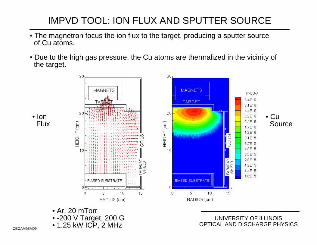
IMPVD TOOL: ION FLUX AND SPUTTER SOURCE
CECAM98M09
• Ar, 20 mTorr• -200 V Target, 200 G• 1.25 kW ICP, 2 MHz
• The magnetron focus the ion flux to the target, producing a sputter source of Cu atoms.
• Due to the high gas pressure, the Cu atoms are thermalized in the vicinity of the target.
• Cu Source
• Ion Flux
UNIVERSITY OF ILLINOISOPTICAL AND DISCHARGE PHYSICS
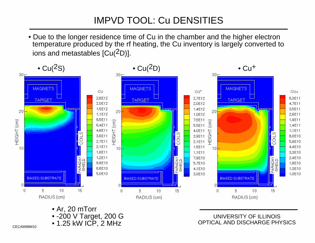
IMPVD TOOL: Cu DENSITIES
CECAM98M10
• Ar, 20 mTorr• -200 V Target, 200 G• 1.25 kW ICP, 2 MHz
• Due to the longer residence time of Cu in the chamber and the higher electron temperature produced by the rf heating, the Cu inventory is largely converted to ions and metastables [Cu(2D)].
• Cu(2S) • Cu(2D) • Cu+
UNIVERSITY OF ILLINOISOPTICAL AND DISCHARGE PHYSICS
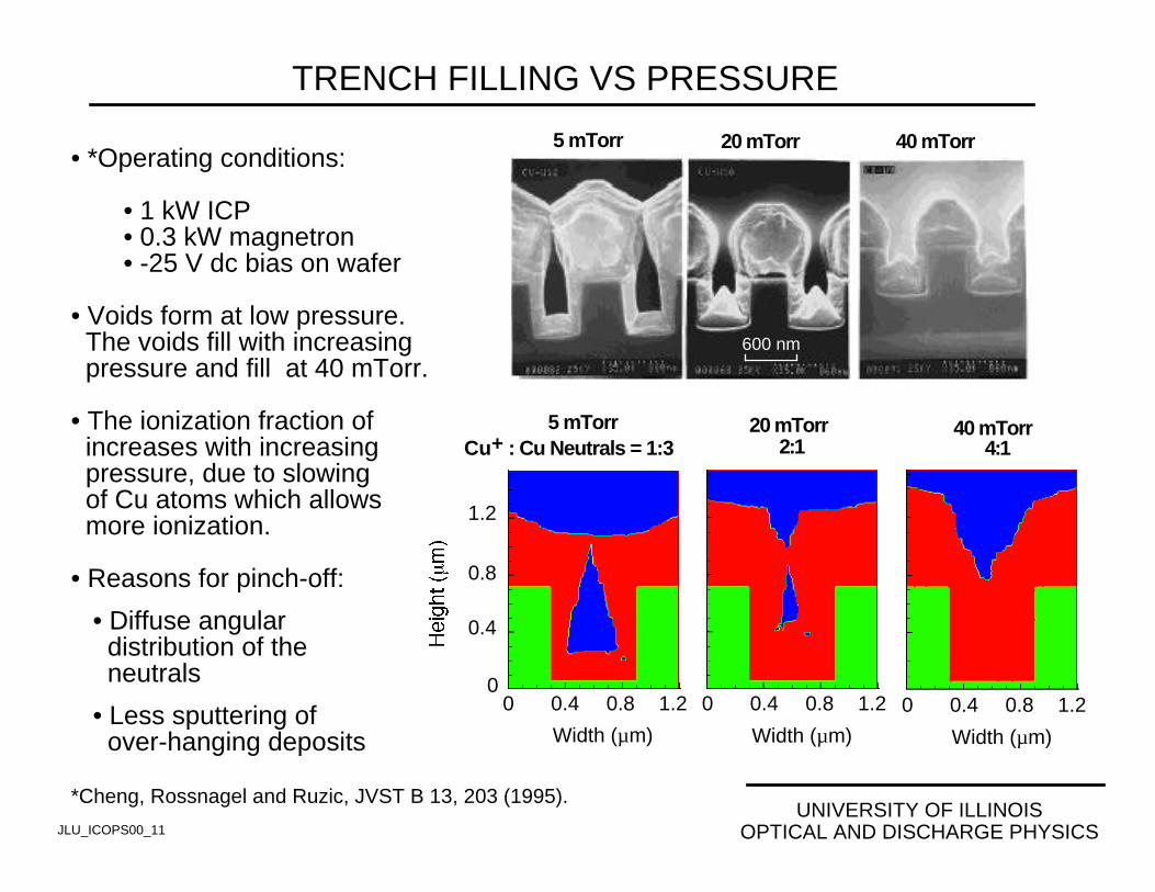
TRENCH FILLING VS PRESSURE
JLU_ICOPS00_11
• *Operating conditions:
• 1 kW ICP • 0.3 kW magnetron• -25 V dc bias on wafer
• Voids form at low pressure. The voids fill with increasing pressure and fill at 40 mTorr.
• The ionization fraction of increases with increasing pressure, due to slowing of Cu atoms which allows more ionization. • Reasons for pinch-off:
• Diffuse angular distribution of the neutrals
• Less sputtering of over-hanging deposits
*Cheng, Rossnagel and Ruzic, JVST B 13, 203 (1995).
Width (µm)
0 0.4 0.8 1.2
0.8
0.4
0
1.2
Cu+ : Cu Neutrals = 1:3 4:12:1
5 mTorr 20 mTorr 40 mTorr
600 nm
Width (µm)
0 0.4 0.8 1.2
Width (µm)
0 0.4 0.8 1.2
5 mTorr 20 mTorr 40 mTorr
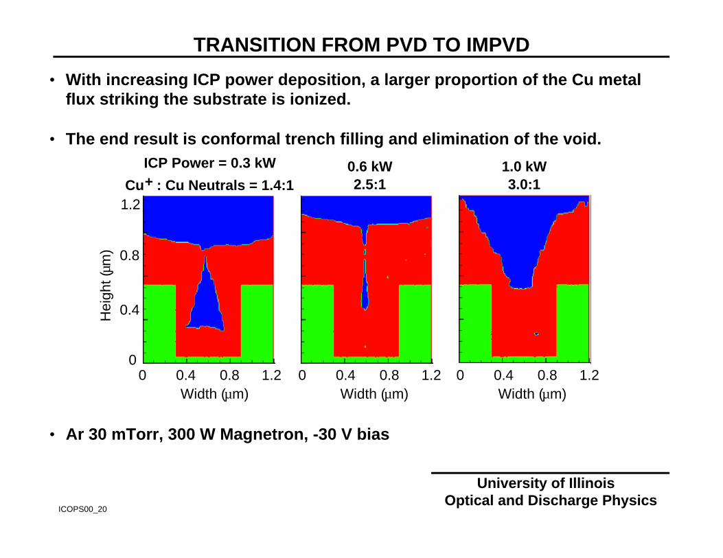
TRANSITION FROM PVD TO IMPVD
ICOPS00_20
University of Illinois Optical and Discharge Physics
• With increasing ICP power deposition, a larger proportion of the Cu metalflux striking the substrate is ionized.
• The end result is conformal trench filling and elimination of the void.ICP Power = 0.3 kW
Cu+ : Cu Neutrals = 1.4:1
Width (µm)0 0.4 0.8 1.2
Hei
ght (
µ m) 0.8
0.4
0
1.2
Width (µm)0 0.4 0.8 1.2
Width (µm)0 0.4 0.8 1.2
0.6 kW 2.5:1
1.0 kW 3.0:1
• Ar 30 mTorr, 300 W Magnetron, -30 V bias
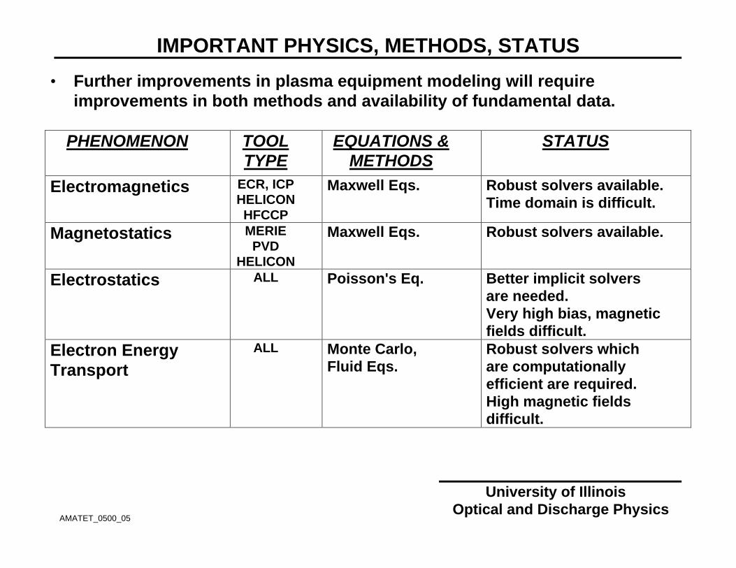
IMPORTANT PHYSICS, METHODS, STATUS
AMATET_0500_05
University of Illinois Optical and Discharge Physics
• Further improvements in plasma equipment modeling will requireimprovements in both methods and availability of fundamental data.
PHENOMENON TOOLTYPE
EQUATIONS &METHODS
STATUS
Electromagnetics ECR, ICPHELICONHFCCP
Maxwell Eqs. Robust solvers available.Time domain is difficult.
Magnetostatics MERIEPVD
HELICON
Maxwell Eqs. Robust solvers available.
Electrostatics ALL Poisson's Eq. Better implicit solversare needed.Very high bias, magneticfields difficult.
Electron EnergyTransport
ALL Monte Carlo,Fluid Eqs.
Robust solvers whichare computationallyefficient are required.High magnetic fieldsdifficult.
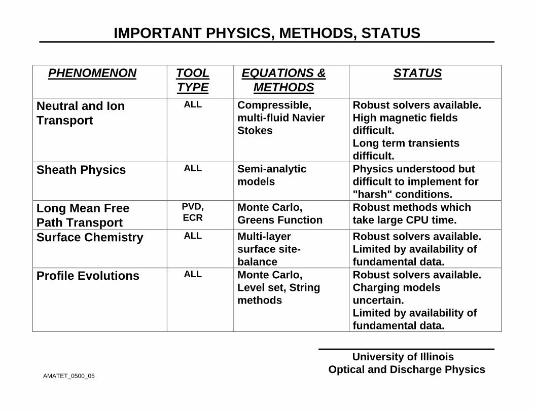
IMPORTANT PHYSICS, METHODS, STATUS
AMATET_0500_05
University of Illinois Optical and Discharge Physics
PHENOMENON TOOLTYPE
EQUATIONS &METHODS
STATUS
Neutral and IonTransport
ALL Compressible,multi-fluid NavierStokes
Robust solvers available.High magnetic fieldsdifficult.Long term transientsdifficult.
Sheath Physics ALL Semi-analyticmodels
Physics understood butdifficult to implement for"harsh" conditions.
Long Mean FreePath Transport
PVD,ECR
Monte Carlo,Greens Function
Robust methods whichtake large CPU time.
Surface Chemistry ALL Multi-layersurface site-balance
Robust solvers available.Limited by availability offundamental data.
Profile Evolutions ALL Monte Carlo,Level set, Stringmethods
Robust solvers available.Charging modelsuncertain.Limited by availability offundamental data.

CONCLUDING REMARKS
AMATET_0500_21
University of Illinois Optical and Discharge Physics
• Plasma equipment modeling has developed to the point that quantitativedesign of tools can be performed and the design cycle can be shortened.
• Process design based on modeling is in a more qualitative state, thoughprogress is being made.
• Significant improvements are required in our databases of fundamentalparameters (e.g., cross sections) so that more complex plasmachemistries can be addressed.

VMIC0002
For a copy of today's presentation......
http://uigelz.ece.uiuc.edu →→ Presentation link at top of page
Related Documents