Planar self-aligned imprint lithography for coplanar plasmonic nanostructures fabrication Weiwei Wan • Liang Lin • Yelong Xu • Xu Guo • Xiaoping Liu • Haixiong Ge • Minghui Lu • Bo Cui • Yanfeng Chen Received: 5 January 2014 / Accepted: 11 February 2014 / Published online: 1 March 2014 Ó Springer-Verlag Berlin Heidelberg 2014 Abstract Nanoimprint lithography (NIL) is a cost-effi- cient nanopatterning technology because of its promising advantages of high throughput and high resolution. How- ever, accurate multilevel overlay capability of NIL required for integrated circuit manufacturing remains a challenge due to the high cost of achieving mechanical alignment precision. Although self-aligned imprint lithog- raphy was developed to avoid the need of alignment for the vertical layered structures, it has limited usage in the manufacture of the coplanar structures, such as integrated plasmonic devices. In this paper, we develop a new process of planar self-alignment imprint lithography (P-SAIL) to fabricate the metallic and dielectric structures on the same plane. P-SAIL transfers the multilevel imprint processes to a single-imprint process which offers higher efficiency and less cost than existing manufacturing methods. Such con- cept is demonstrated in an example of fabricating planar plasmonic structures consisting of different materials. 1 Introduction Nanoimprint lithography (NIL) [1] has been demonstrated as a low-cost technology for the mass production of nanostructures with high resolutions. Unlike a traditional UV optical lithography whose resolution is dependent upon the optical wavelength, the pattern replication in NIL is achieved directly by a mechanical deformation process, which is completely free from the diffraction limit and capable of achieving sub-10 nm features [2, 3]. The NIL technology has wide applications in the fields of electronics [4], photonics [5] and bioscience [6]. However, in order to compete with the UV lithography dominantly used in microelectronics industry, the overlay accuracy issue of NIL in a multi-step fabrication process has to be solved. The Moire ´ fringe generated by overlaying two sets of gratings is usually used to control the alignment of two NIL steps [7, 8]. However, the additional imprint module and imaging system could dramatically increase the cost. Although the overlay accuracy better than 20 nm has been achieved, the intrinsic error of overlay alignment cannot be eliminated which is limited by the inevitable mechanical and thermal instability. On the other hand, the high-speed roll-to-roll (R2R) processes have made NIL a very competitive technique for the high-throughput and low-cost manufacturing of large-area circuitry [9]. The combination of an additional alignment system to the R2R processes in order to pro- duce overlaid structures is difficult, and it would also slow down the manufacture. Under such scenario, self-aligned imprint lithography (SAIL) [10] was developed. SAIL does not need alignment because the geometry informa- tion of the entire patterning steps is encoded onto different heights of the molding structures. By alternately etching the masking structure and the thin-film stack, the patterns W. Wan (&) Á L. Lin Á Y. Xu Á X. Guo Á X. Liu Á H. Ge Á M. Lu Á Y. Chen National Laboratory of Solid State Microstructures and Department of Materials Science and Engineering, Nanjing University, Nanjing 210093, People’s Republic of China e-mail: [email protected] M. Lu e-mail: [email protected] B. Cui Department of Electrical and Computer Engineering, Waterloo Institute for Nanotechnology, University of Waterloo, Waterloo, ON N2L3G1, Canada 123 Appl. Phys. A (2014) 116:657–662 DOI 10.1007/s00339-014-8323-5

Welcome message from author
This document is posted to help you gain knowledge. Please leave a comment to let me know what you think about it! Share it to your friends and learn new things together.
Transcript
Planar self-aligned imprint lithography for coplanar plasmonicnanostructures fabrication
Weiwei Wan • Liang Lin • Yelong Xu •
Xu Guo • Xiaoping Liu • Haixiong Ge •
Minghui Lu • Bo Cui • Yanfeng Chen
Received: 5 January 2014 / Accepted: 11 February 2014 / Published online: 1 March 2014
� Springer-Verlag Berlin Heidelberg 2014
Abstract Nanoimprint lithography (NIL) is a cost-effi-
cient nanopatterning technology because of its promising
advantages of high throughput and high resolution. How-
ever, accurate multilevel overlay capability of NIL
required for integrated circuit manufacturing remains a
challenge due to the high cost of achieving mechanical
alignment precision. Although self-aligned imprint lithog-
raphy was developed to avoid the need of alignment for the
vertical layered structures, it has limited usage in the
manufacture of the coplanar structures, such as integrated
plasmonic devices. In this paper, we develop a new process
of planar self-alignment imprint lithography (P-SAIL) to
fabricate the metallic and dielectric structures on the same
plane. P-SAIL transfers the multilevel imprint processes to
a single-imprint process which offers higher efficiency and
less cost than existing manufacturing methods. Such con-
cept is demonstrated in an example of fabricating planar
plasmonic structures consisting of different materials.
1 Introduction
Nanoimprint lithography (NIL) [1] has been demonstrated
as a low-cost technology for the mass production of
nanostructures with high resolutions. Unlike a traditional
UV optical lithography whose resolution is dependent upon
the optical wavelength, the pattern replication in NIL is
achieved directly by a mechanical deformation process,
which is completely free from the diffraction limit and
capable of achieving sub-10 nm features [2, 3]. The NIL
technology has wide applications in the fields of electronics
[4], photonics [5] and bioscience [6]. However, in order to
compete with the UV lithography dominantly used in
microelectronics industry, the overlay accuracy issue of
NIL in a multi-step fabrication process has to be solved.
The Moire fringe generated by overlaying two sets of
gratings is usually used to control the alignment of two NIL
steps [7, 8]. However, the additional imprint module and
imaging system could dramatically increase the cost.
Although the overlay accuracy better than 20 nm has been
achieved, the intrinsic error of overlay alignment cannot be
eliminated which is limited by the inevitable mechanical
and thermal instability.
On the other hand, the high-speed roll-to-roll (R2R)
processes have made NIL a very competitive technique
for the high-throughput and low-cost manufacturing of
large-area circuitry [9]. The combination of an additional
alignment system to the R2R processes in order to pro-
duce overlaid structures is difficult, and it would also slow
down the manufacture. Under such scenario, self-aligned
imprint lithography (SAIL) [10] was developed. SAIL
does not need alignment because the geometry informa-
tion of the entire patterning steps is encoded onto different
heights of the molding structures. By alternately etching
the masking structure and the thin-film stack, the patterns
W. Wan (&) � L. Lin � Y. Xu � X. Guo � X. Liu � H. Ge �M. Lu � Y. Chen
National Laboratory of Solid State Microstructures and
Department of Materials Science and Engineering, Nanjing
University, Nanjing 210093, People’s Republic of China
e-mail: [email protected]
M. Lu
e-mail: [email protected]
B. Cui
Department of Electrical and Computer Engineering, Waterloo
Institute for Nanotechnology, University of Waterloo, Waterloo,
ON N2L3G1, Canada
123
Appl. Phys. A (2014) 116:657–662
DOI 10.1007/s00339-014-8323-5
are transferred to the device vertical layers. The R2R
based on SAIL is successfully used to make thin-film
transistor arrays on meter-scaled flexible substrates [11].
However, such technology has not been easily adopted to
fabricate an important class of devices in the field of
nanophotonics. For example, the coplanar metallic and
dielectric structures have attracted lots of research interest,
which can be artificially designed and fabricated to
manipulate light propagation and behaviors, such as three-
dimensional nanolens [12], plasmonic waveguides [13],
single-layer negative-index metamaterials [14], unidirec-
tional reflectionless parity-time metamaterials [15]. Fab-
ricating both metallic and dielectric structures on the same
plane without geometry offset is very challenging for the
current SAIL processes. In this work, we have developed
planar self-aligned imprint lithography (P-SAIL) to over-
come the above challenge in SAIL process. P-SAIL
encodes all of the patterning information onto a multilevel
mold. By alternately etching the masking structure and
depositing thin films, the patterns are transferred to the
planar features. The alignment accuracy is maintained by
the pre-aligned mask structures and is unaffected by the
deformation or distortion induced in the subsequent pro-
cesses. P-SAIL simplifies multilevel imprint processes to a
single-imprint process, which makes it easy to integrate
with R2R processes. The P-SAIL offers greater efficiency
and less cost than the existing manufacturing methods for
planar structures composed of different materials, and it
shows great potentials in the field of plasmonic integrated
optics.
2 The planar self-aligned nanolithography process
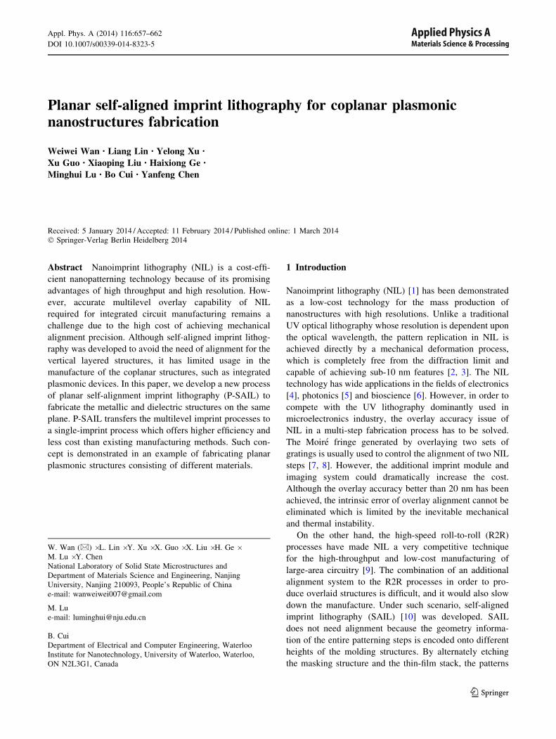
The proposed P-SAIL fabrication steps are illustrated in
Fig. 1. The multilevel imprinted mold has patterns encoded
on two different heights. These patterns are then transferred
to the resist layer on a silicon (Si) substrate by NIL, which is
followed by an O2 plasma etching with a careful control in
timing in order to remove only the thinnest residual resist
layer so as to expose partially the substrate. The remaining
resist serves as the etching mask for the pattern transferring
to the silicon substrate. The etching recipe is optimized to
achieve almost the same etching rate for the resist and sili-
con, in order to replicate the patterns with different heights
on the silicon substrate (Fig. 1d). Then, the substrate is spin-
coated with the resist again to cover all the patterns, followed
by the etching with an O2 plasma until the higher silicon
structures are exposed. Another etching recipe which has
high etching selectivity for the resist over silicon is used to
etch the exposed silicon (Fig. 1g). Then, the metallic layer is
deposited, followed by a lift-off process using acetone
forming the final structures on the same plane.
There are two key points in P-SAIL processes: (1)
precise removal of the resist and silicon. For the steps (c) to
(d) as shown in Fig 1, a similar etching rate for the resist
and silicon is required. Whereas for the steps (f) to (g), a
high etching selectivity for the resist over silicon is needed.
(2) Flatness of the top resist layer during the second spin-
coating process (Fig. 1e). More details about the P-SAIL
flow and how to address the above two challenges will be
discussed in the next section.
Fig. 1 Schematic of planar
self-aligned imprint lithography
process. All the information of
two-level patterns is pre-aligned
and encoded in the imprint
mold. The patterns are
transferred to the coplanar
features by a set of nanoimprint,
dry etching and film deposition
processes
658 W. Wan et al.
123
3 Experimental results and discussion
3.1 Mold fabrication and NIL
The multilevel imprint mold plays an important role in the
P-SAIL. All the patterns are pre-aligned on the mold, and
there is no requirement for overlay alignment during
P-SAIL processes. The alignment accuracy is only limited
by the technique used to fabricate the mold, which can
easily achieve sub-10 nm by focused ion beam lithography
(FIB). Note that electron beam lithography using double-
layer resist stack may also be used to fabricate the bi-level
imprint mold [16]. In order to minimize the thermal mis-
match between the mold and the substrate, we choose sil-
icon as the mold material and use FIB to fabricate patterns
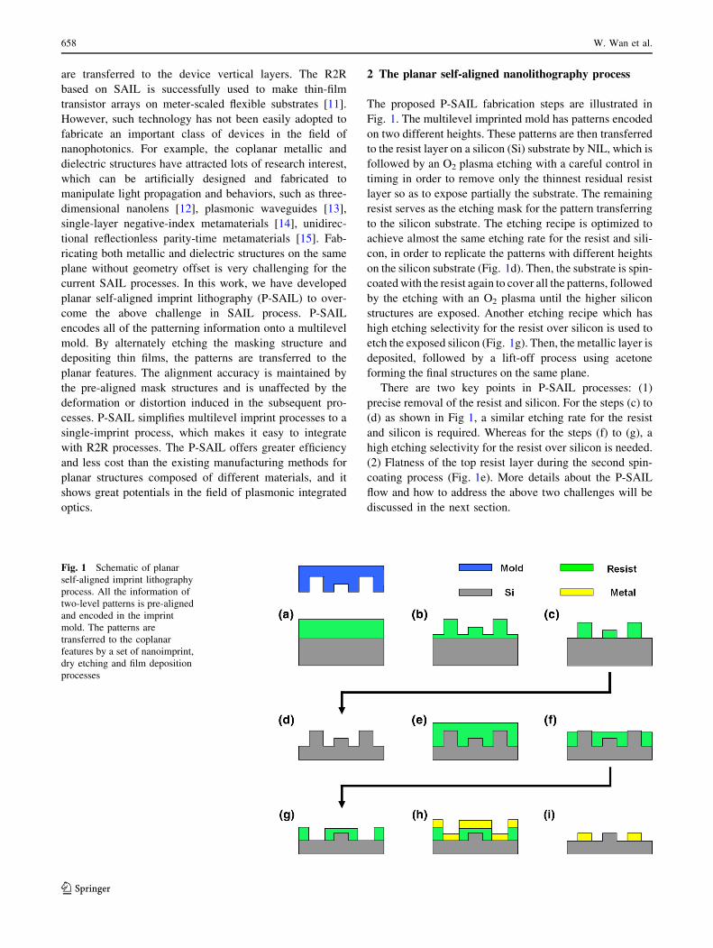
corresponding to two different heights on it. As shown in
Fig. 2a, the period (P) of these patterns is 1 lm. The height
(H1) of the gap is about 350 nm, with the width (W) of
180 nm. The height of the middle square (H2) is about
120 nm with the length (L) of 400 nm. The total area of
these patterns is 10 9 10 lm. To assist the releasing of the
mold, a surfactant (1H, 1H, 2H, 2H-perfluorooctyl-tri-
chlorosilane) is coated on the silicon mold to reduce its
surface energy and prevent the resist material from sticking
on it during the NIL process.
Before imprinting, a thermal resist layer with the
thickness of 180 nm was spin-coated on a silicon substrate.
The thermal NIL was carried out by a commercial nano-
imprint machine (YPL-NIL-SI400 manufactured by
Imprint Nano Co. Ltd) at a temperature of 130 �C and a
pressure of 0.3 MPa. A thicker resist layer whose height is
comparable with the largest height (H1) on the mold is not
preferred, because the total pattern area is quite small
(*100 lm2) compared to the size of the substrate. After
imprinting, the thickness of the residual layer would be the
same as that of the spin-coated layer. Thick residual layer
would require longer etching time during the removal
process, which often degrades the resolution and fidelity of
the pattern. Instead, we used a resist layer with the thick-
ness of 180 nm which is thick enough to replicate the
patterns on the mold. As shown in Fig. 2b, the two-level
pattern information was successfully transferred to the
thermoplastic resist. The height of the fishnet is about
300 nm, and the height of the middle squares is about
100 nm.
3.2 Spin coating and dry etching
As mentioned above, the precise removal of the polymer
resist and the silicon is of significant importance in
P-SAIL. In order to obtain the applicable etching rates for
the resist and silicon, comprehensive dry etching tests were
carried out with a number of recipes by a high-density
plasma etching system (ULVAC CE-300I). For each
etching recipe, the pressure is fixed at a low value (0.5 Pa)
to facilitate etching species/products to get into/out of high-
aspect-ratio structures. Several combinations of etching gas
(O2, CHF3, CF4, SF6) and different etching powers were
employed and investigated. The etching selectivity of the
resist and silicon can be realized by controlling the ratio of
reactive gases (oxygen and fluorides). The etching rate of
Si can be adjusted by the plasma density of F- provided by
various fluorides. Our comprehensive etching study yields
three recipes for the P-SAIL process, which are shown in
Table 1. Recipe A contains only O2 and is used to etch the
polymer resist during the steps (b)–(c) and (e)–(f) as shown
in Fig. 1. The etching rate of the resist is about 45 nm/min.
Recipe B contains O2 and fluorides, which is used during
the steps (d)–(e) to etch both the resist and silicon at almost
the same etching rate, i.e., about 27 nm/min. The Bias
power is applied to provide anisotropic etching in order to
have a vertical sidewall. Recipe C does not contain O2 in
order to avoid the etching of the polymer mask during the
steps (f)–(g). The Bias power is not applied in this case to
minimize the ion bombardment of the polymer mask.
Instead, we introduced more CF4 and SF6 in the etchant, as
Fig. 2 a Two-level silicon imprint mold fabricated by FIB. The total
area of these patterns is 10 9 10 lm, with the period (P) of 1 lm.
The height (H1) of the gap is about 350 nm, with the width (W) of
180 nm. The height of the middle square (H2) is about 120 nm with
the length (L) of 400 nm. b The nanoimprint result. The heights of the
fishnet and middle square are about 300 and 100 nm, respectively
Planar self-aligned imprint lithography 659
123
well as a higher source RF power to increase the density of
F- for silicon etching. Under these optimizations, the
etching rate of silicon is about 30 nm/min with a good
etching selectivity of 20:1 to the resist.
Based on the three recipes in Table 1, the 180 nm
residual layer on the sample (as shown in Fig. 2b) was
etched using recipe A for 4 min, followed by recipe B for
11 min to transfer the two-level patterns to the silicon
substrate. The sample was then soaked in acetone to
remove the remaining polymer resist. After blow drying
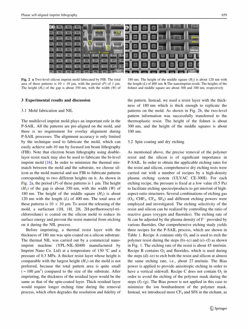
with N2, the sample was spin-coated with a 340-nm resist
layer. Because of the nonflat substrate, the resist layer has
surface topographies. In order to planarize the top layer, the
sample was thermally imprinted with a flat silicon mold.
As a result, the top surface of the resist layer was suc-
cessfully planarized, with the maximum surface roughness
being \4 nm, as shown in the AFM image in Fig. 3. The
planarization of the spin-coated resist film on a nonflat
silicon substrate could also be achieved by increasing the
thickness of the resist film. However, this approach would
require more resist materials as well as longer etching time
to etch through the thick planarization layer, which in turn
would increase the cost and degrade the fidelity of the
patterns. Instead, using an NIL process for resist planari-
zation here can be cost-effective.
After the 340-nm flat resist layer is formed on the sur-
face, recipe A was used again (etching time: 1 min) to
remove a certain amount of the top resist layer exposing the
higher silicon structures, followed by a etching with recipe
C to etch the exposed higher silicon structures (its height is
about 300 nm) for 10 min. Finally, the sample was ther-
mally evaporated with 160 nm chromium (Cr). The resist
was then removed by ultrasonic lift-off process in acetone
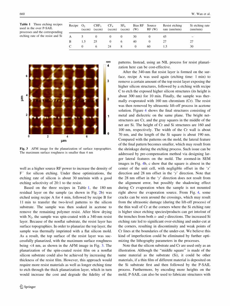
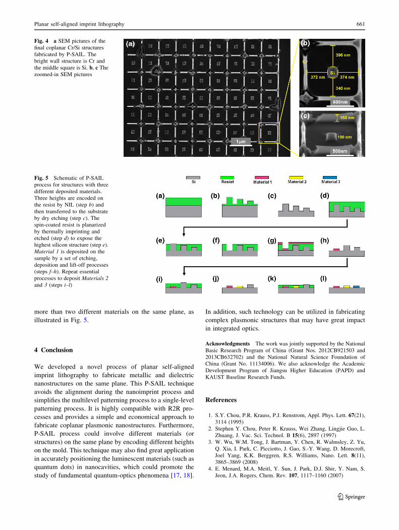
solution. Figure 4 shows the final structures consisting of
metal and dielectric on the same plane. The bright net-
structures are Cr, and the gray squares in the middle of the
net are Si. The height of Cr and Si structures are 160 and
100 nm, respectively. The width of the Cr wall is about
70 nm, and the length of the Si square is about 190 nm.
Compared with the patterns on the mold, the lateral feature
of the final pattern becomes smaller, which may result from
the shrinkage during the etching process. Such issue can be
addressed by pre-compensation method via designing lar-
ger lateral features on the mold. The zoomed-in SEM
images in Fig. 4b, c show that the square is almost in the
center of the unit cell, with negligible offset in the ‘x’
direction and 28 nm offset in the ‘y’ direction. Note that
the 28 nm offset in the ‘y’ direction does not result from
the alignment error, but possibly the shadowing effect
during Cr evaporation when the sample is not mounted
right above the evaporation source. From Fig. 4, some
cracks can be seen around the crossings, which may result
from the ultrasonic damage (during the lift-off process) of
the thin wall of Cr at the corners where the Si etching rate
is higher since etching species/products can get into/out of
the trenches from both x- and y-directions. The increased Si
etching rate led to significant over-etching and under-cut at
the corners, resulting in discontinuity and weak points of
Cr lines at the boundaries of the under-cut. We believe this
kind of imperfection could be eliminated by further opti-
mizing the lithography parameters in the processes.
Note that the silicon substrate and Cr are used only as an
illustration. Although the ‘‘middle square’’ is made of the
same material as the substrate (Si), it could be other
materials, if a thin film of different material is deposited on
the Si substrate first and then followed by the P-SAIL
process. Furthermore, by encoding more heights on the
mold, P-SAIL can also be used to fabricate structures with
Fig. 3 AFM image for the planarization of surface topographies.
The maximum surface roughness is smaller than 4 nm
Table 1 Three etching recipes
used in the over P-SAIL
processes and the corresponding
etching rate of the resist and Si
Recipe O2
(sccm)
CHF3
(sccm)
CF4
(sccm)
SF6
(sccm)
Bias RF
(W)
Source
RF (W)
Resist etching
rate (nm/min)
Si etching rate
(nm/min)
A 5 0 0 0 30 0 45 –
B 1.5 25 0 6 40 0 27 27
C 0 6 24 8 0 60 1.5 30
660 W. Wan et al.
123
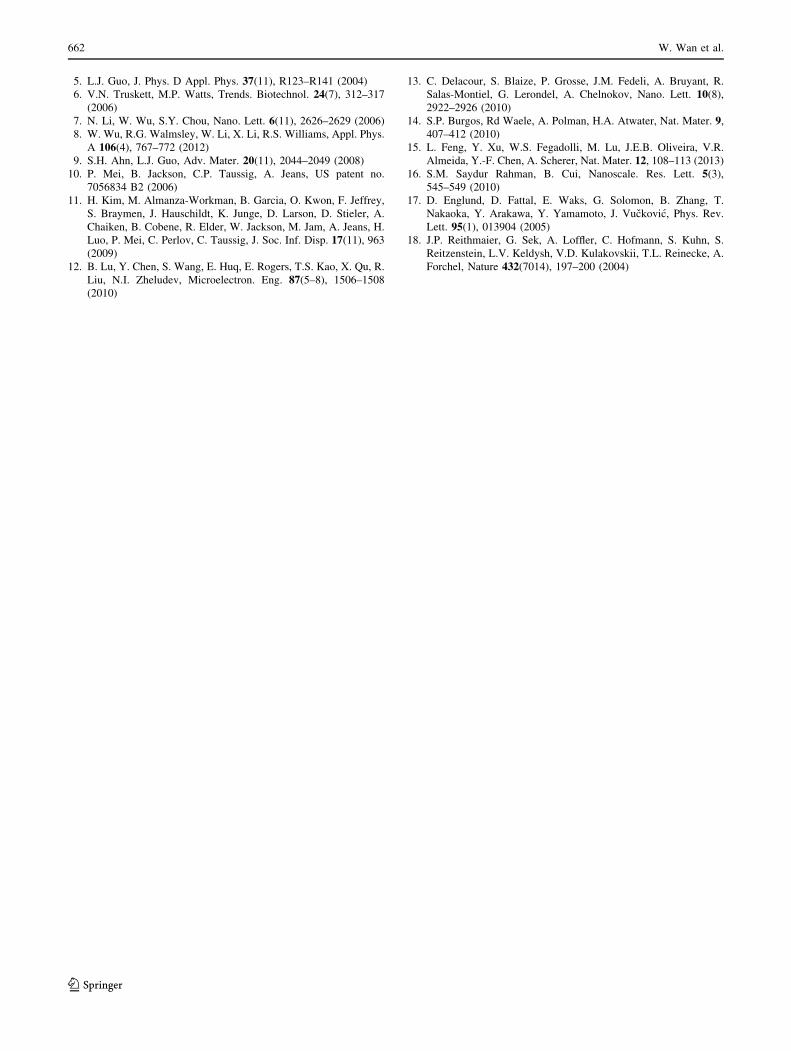
more than two different materials on the same plane, as
illustrated in Fig. 5.
4 Conclusion
We developed a novel process of planar self-aligned
imprint lithography to fabricate metallic and dielectric
nanostructures on the same plane. This P-SAIL technique
avoids the alignment during the nanoimprint process and
simplifies the multilevel patterning process to a single-level
patterning process. It is highly compatible with R2R pro-
cesses and provides a simple and economical approach to
fabricate coplanar plasmonic nanostructures. Furthermore,
P-SAIL process could involve different materials (or
structures) on the same plane by encoding different heights
on the mold. This technique may also find great application
in accurately positioning the luminescent materials (such as
quantum dots) in nanocavities, which could promote the
study of fundamental quantum-optics phenomena [17, 18].
In addition, such technology can be utilized in fabricating
complex plasmonic structures that may have great impact
in integrated optics.
Acknowledgments The work was jointly supported by the National
Basic Research Program of China (Grant Nos. 2012CB921503 and
2013CB632702) and the National Natural Science Foundation of
China (Grant No. 11134006). We also acknowledge the Academic
Development Program of Jiangsu Higher Education (PAPD) and
KAUST Baseline Research Funds.
References
1. S.Y. Chou, P.R. Krauss, P.J. Renstrom, Appl. Phys. Lett. 67(21),
3114 (1995)
2. Stephen Y. Chou, Peter R. Krauss, Wei Zhang, Lingjie Guo, L.
Zhuang, J. Vac. Sci. Technol. B 15(6), 2897 (1997)
3. W. Wu, W.M. Tong, J. Bartman, Y. Chen, R. Walmsley, Z. Yu,
Q. Xia, I. Park, C. Picciotto, J. Gao, S.-Y. Wang, D. Morecroft,
Joel Yang, K.K. Berggren, R.S. Williams, Nano. Lett. 8(11),
3865–3869 (2008)
4. E. Menard, M.A. Meitl, Y. Sun, J. Park, D.J. Shir, Y. Nam, S.
Jeon, J.A. Rogers, Chem. Rev. 107, 1117–1160 (2007)
Fig. 4 a SEM pictures of the
final coplanar Cr/Si structures
fabricated by P-SAIL. The
bright wall structure is Cr and
the middle square is Si. b, c The
zoomed-in SEM pictures
Fig. 5 Schematic of P-SAIL
process for structures with three
different deposited materials.
Three heights are encoded on
the resist by NIL (step b) and
then transferred to the substrate
by dry etching (step c). The
spin-coated resist is planarized
by thermally imprinting and
etched (step d) to expose the
highest silicon structure (step e).
Material 1 is deposited on the
sample by a set of etching,
deposition and lift-off processes
(steps f–h). Repeat essential
processes to deposit Materials 2
and 3 (steps i–l)
Planar self-aligned imprint lithography 661
123
5. L.J. Guo, J. Phys. D Appl. Phys. 37(11), R123–R141 (2004)
6. V.N. Truskett, M.P. Watts, Trends. Biotechnol. 24(7), 312–317
(2006)
7. N. Li, W. Wu, S.Y. Chou, Nano. Lett. 6(11), 2626–2629 (2006)
8. W. Wu, R.G. Walmsley, W. Li, X. Li, R.S. Williams, Appl. Phys.
A 106(4), 767–772 (2012)
9. S.H. Ahn, L.J. Guo, Adv. Mater. 20(11), 2044–2049 (2008)
10. P. Mei, B. Jackson, C.P. Taussig, A. Jeans, US patent no.
7056834 B2 (2006)
11. H. Kim, M. Almanza-Workman, B. Garcia, O. Kwon, F. Jeffrey,
S. Braymen, J. Hauschildt, K. Junge, D. Larson, D. Stieler, A.
Chaiken, B. Cobene, R. Elder, W. Jackson, M. Jam, A. Jeans, H.
Luo, P. Mei, C. Perlov, C. Taussig, J. Soc. Inf. Disp. 17(11), 963
(2009)
12. B. Lu, Y. Chen, S. Wang, E. Huq, E. Rogers, T.S. Kao, X. Qu, R.
Liu, N.I. Zheludev, Microelectron. Eng. 87(5–8), 1506–1508
(2010)
13. C. Delacour, S. Blaize, P. Grosse, J.M. Fedeli, A. Bruyant, R.
Salas-Montiel, G. Lerondel, A. Chelnokov, Nano. Lett. 10(8),
2922–2926 (2010)
14. S.P. Burgos, Rd Waele, A. Polman, H.A. Atwater, Nat. Mater. 9,
407–412 (2010)
15. L. Feng, Y. Xu, W.S. Fegadolli, M. Lu, J.E.B. Oliveira, V.R.
Almeida, Y.-F. Chen, A. Scherer, Nat. Mater. 12, 108–113 (2013)
16. S.M. Saydur Rahman, B. Cui, Nanoscale. Res. Lett. 5(3),
545–549 (2010)
17. D. Englund, D. Fattal, E. Waks, G. Solomon, B. Zhang, T.
Nakaoka, Y. Arakawa, Y. Yamamoto, J. Vuckovic, Phys. Rev.
Lett. 95(1), 013904 (2005)
18. J.P. Reithmaier, G. Sek, A. Loffler, C. Hofmann, S. Kuhn, S.
Reitzenstein, L.V. Keldysh, V.D. Kulakovskii, T.L. Reinecke, A.
Forchel, Nature 432(7014), 197–200 (2004)
662 W. Wan et al.
123
Related Documents


