Planar Antennas for Multiband and Ultra-Wideband Communications by Iftikhar Ahmed MT-133017 A thesis submitted to the Electrical Engineering Department in partial fulfillment of the requirements for the degree of MS IN ELECTRONIC ENGINEERING Faculty of Engineering Capital University of Science and Technology Islamabad September 2017

Welcome message from author
This document is posted to help you gain knowledge. Please leave a comment to let me know what you think about it! Share it to your friends and learn new things together.
Transcript
Planar Antennas for Multibandand Ultra-WidebandCommunications
by
Iftikhar Ahmed
MT-133017
A thesis submitted to theElectrical Engineering Department
in partial fulfillment of the requirements for the degree ofMS IN ELECTRONIC ENGINEERING
Faculty of EngineeringCapital University of Science and Technology
Islamabad
September 2017

Copyright c© 2017 by Iftikhar Ahmed
All rights reserved. Replication in any form requires the prior written permissionof author or designated representative.
i

DECLARATION
It is declared that this is an original piece of my own work, except where other-wise acknowledged in text and references. This work has not been submitted inany form for another degree or diploma at any university or other institution fortertiary education and shall not be submitted by me in future for obtaining anydegree.
Iftikhar AhmedMT-133017
September 2017
ii

Dedicated to my parents and my elder brother for their affectionatelove, moral support and encouragement
iii
CERTIFICATE OF APPROVAL
Planar Antennas for Multiband and Ultra-WidebandCommunications
byIftikhar Ahmed
MT-133017
THESIS EXAMINING COMMITTEE
S. No. Examiner Name Organization
(a) External Examiner Dr. Junaid Mughal COMSATS, Islamabad
(b) Internal Examiner Dr. M. Mansoor Ahmed CUST, Islamabad
(c) Supervisor Dr. Ali Imran Najam CESAT, Islamabad
Dr. Ali Imran Najam
Thesis Supervisor
September, 2017
Dr. Noor Muhammad Khan Dr. Imtiaz Ahmed Taj
Head Dean
Dept. of Electrical Engineering Faculty of Engineering
September, 2017 September, 2017
iv

CERTIFICATE OF CHANGES
This is to certify that Mr. Iftikhar Ahmed has incorporated all observations, sug-gestions and comments made by external as well as internal examiner and thesissupervisor.
Dr. Ali Imran Najam
(Thesis Supervisor)
v

ACKNOWLEDGMENT
First and foremost I would like to thank Allah Almighty, who gave me the courageto continue my graduate studies with research work. The determination grantedby Allah helped me to tolerate the hard times to produce this thesis.
I would like to express my gratitude to my supervisor Dr. Ali Imran Najamfor his guidance, support and encouragement. My research work is the result ofhis determination, appreciation and creative thinking. His exceptional theoreticalconcepts and research experience helped me during this research work. Workingwith him has been a great experience for me. Without his guidance and supportthis thesis would never been accomplished.
I would like to thank Mr. Umair Rafique, Research Associate in Electrical En-gineering Department at Capital University for Science and Technology, for hisguidance and help throughout this research work. His motivation and encourage-ment helped me a lot to complete this thesis. Working with him has been a greatexperience.
I want to appreciate all teachers of Capital University of Science and Technology,who taught me during my course work, by delivering their precious and valuablethoughts, in building my concepts.
vi
ABSTRACT
This thesis focuses on planar monopole antenna designs and analysis. Extensiveinvestigations are also carried out on two different planar antennas.
In the first part, a multiband planar monopole antenna is designed for GSM,DCS, WiMAX and WLAN communications. The proposed antenna consists of aG-shaped and inverted L-shaped radiators, which are connected with each other.The G-shaped radiator is responsible to offer GSM (1800 MHz), WLAN (2.45GHz) and WiMAX (3.5 GHz) frequency bands, while inverted L-shaped radiatoris able to provide GSM (900 MHz) and WLAN (5.25 GHz) frequency bands.It is also observed that the proposed multiband antenna offered good radiationcharacteristics and gain for desired frequency bands.
In the second part of this thesis, the design of a compact planar monopole an-tenna is presented for UWB and two extra GSM frequency bands. A hexagonal-shaped patch is used to achieve UWB response. Two Capacitive Loaded Res-onators (CLRs) are employed with a ground plane to obtain resonance at 900 and1800 MHz. Measurements are carried out to verify simulation results, and it isobserved that the measured and simulated results are in agreement. Furthermore,good radiation characteristics and gain is obtained from the proposed design.
It is also observed that the proposed antennas are small in size. These features havedemonstrated that the proposed antennas can be an excellent choice for variouswireless communication systems.
vii

TABLE OF CONTENTS
Declaration . . . . . . . . . . . . . . . . . . . . . . . . . . . . . . . . . . . iiAcknowledgment . . . . . . . . . . . . . . . . . . . . . . . . . . . . . . . . viAbstract . . . . . . . . . . . . . . . . . . . . . . . . . . . . . . . . . . . . . viiTable of Contents . . . . . . . . . . . . . . . . . . . . . . . . . . . . . . . . viiiList of Figures . . . . . . . . . . . . . . . . . . . . . . . . . . . . . . . . . xList of Tables . . . . . . . . . . . . . . . . . . . . . . . . . . . . . . . . . . xiList of Acronyms . . . . . . . . . . . . . . . . . . . . . . . . . . . . . . . . xiiList of Symbols . . . . . . . . . . . . . . . . . . . . . . . . . . . . . . . . . xiii
Chapter 1Introduction . . . . . . . . . . . . . . . . . . . . . . . . . . . . . . . . . 11.1 Motivation . . . . . . . . . . . . . . . . . . . . . . . . . . . . . . . 11.2 Research Objectives . . . . . . . . . . . . . . . . . . . . . . . . . . 31.3 Thesis Organization . . . . . . . . . . . . . . . . . . . . . . . . . . 31.4 Key Contributions . . . . . . . . . . . . . . . . . . . . . . . . . . 3
Chapter 2Literature Review . . . . . . . . . . . . . . . . . . . . . . . . . . . . . . 52.1 Historical Background . . . . . . . . . . . . . . . . . . . . . . . . 52.2 Model History . . . . . . . . . . . . . . . . . . . . . . . . . . . . . 52.3 Dual, Tri and Multiband Antennas . . . . . . . . . . . . . . . . . 62.4 UWB Antennas with Extra Bands . . . . . . . . . . . . . . . . . . 92.5 Summary . . . . . . . . . . . . . . . . . . . . . . . . . . . . . . . 12
Chapter 3Multiband Planar Monopole Antenna . . . . . . . . . . . . . . . . . . . 133.1 Proposed Antenna Design . . . . . . . . . . . . . . . . . . . . . . 133.2 Results and Discussion . . . . . . . . . . . . . . . . . . . . . . . . 153.3 Comparative Analysis . . . . . . . . . . . . . . . . . . . . . . . . 193.4 Summary . . . . . . . . . . . . . . . . . . . . . . . . . . . . . . . 19
Chapter 4Planar Antenna for Cellular and Ultra-Wideband Communications . . 214.1 Antenna Design . . . . . . . . . . . . . . . . . . . . . . . . . . . . 214.2 Results and Discussion . . . . . . . . . . . . . . . . . . . . . . . . 234.3 Comparative Analysis . . . . . . . . . . . . . . . . . . . . . . . . 284.4 Summary . . . . . . . . . . . . . . . . . . . . . . . . . . . . . . . 28
Chapter 5Conclusion and Future Work . . . . . . . . . . . . . . . . . . . . . . . . 305.1 Conclusion . . . . . . . . . . . . . . . . . . . . . . . . . . . . . . . 30
viii

5.2 Future work . . . . . . . . . . . . . . . . . . . . . . . . . . . . . . 31
References . . . . . . . . . . . . . . . . . . . . . . . . . . . . . . . . . . . . 32
ix
LIST OF FIGURES
2.1 Design layout of the planar monopole antenna for tri-band charac-teristics [23]. . . . . . . . . . . . . . . . . . . . . . . . . . . . . . . 8
2.2 Geometry of the paw-shaped planar monopole antenna [28]. . . . 82.3 Design and geometry of UWB antenna with integrated Bluetooth
band [33]. . . . . . . . . . . . . . . . . . . . . . . . . . . . . . . . 102.4 Slot antenna configuration for multiband and UWB applications [40]. 11
3.1 Geometry of the proposed multiband planar monopole antenna andit’s parameters (in mm). . . . . . . . . . . . . . . . . . . . . . . . 14
3.2 Return loss results of the two designed antennas. . . . . . . . . . 153.3 Prototype of the proposed multiband planar monopole antenna. . 163.4 Simulated and measured return loss of the proposed multiband pla-
nar monopole antenna. . . . . . . . . . . . . . . . . . . . . . . . . 163.5 Simulated gain of the proposed multiband planar monopole antenna. 173.6 Simulated radiation pattern of the proposed planar monopole an-
tenna at (a) 900 MHz, (b) 1800 MHz, (c) 2.45 GHz, (d) 3.5 GHzand (e) 5.16 GHz (Solid line: E-plane, Dashed line: H-plane). . . 18
4.1 Geometry of the proposed planar monopole antenna. . . . . . . . 224.2 Return loss results for the UWB antenna with added single and
dual-bands. . . . . . . . . . . . . . . . . . . . . . . . . . . . . . . 234.3 Simulated and measured return loss of the proposed planar monopole
antenna. . . . . . . . . . . . . . . . . . . . . . . . . . . . . . . . . 244.4 Prototype of the proposed planar monopole antenna (a) Front view
(b) Back view. . . . . . . . . . . . . . . . . . . . . . . . . . . . . . 244.5 Surface current distribution at (a) 900 MHz (b) 1800 MHz. . . . . 254.6 Simulated gain of the proposed planar monopole antenna. . . . . . 264.7 Simulated radiation pattern of the proposed planar monopole an-
tenna at (a) 900 MHz, (b) 1800 MHz, (c) 3 GHz, (d) 6 GHz and(e) 9.5 GHz (Solid line: E-plane, Dashed line: H-plane). . . . . . . 27
x

LIST OF TABLES
3.1 Comparison of the proposed antenna with previous antennas . . . 19
4.1 Design parameters of the proposed planar monopole antenna [inmm]. . . . . . . . . . . . . . . . . . . . . . . . . . . . . . . . . . . 22
4.2 Comparison between the proposed antenna and previous antennas 28
xi
LIST OF ACRONYMS
CLRs Capacitive Loaded ResonatorsCLLRs Capacitive Loaded Line ResonatorsCPW Coplanar WaveguideDCS Digital Cellular SystemDGS Defected Ground StructureEM ElectromagneticEMC/EMI Electromagnetic Compatibility/InterferenceFCC Federal Communication CommissionGPS Global Positioning SystemGSM Global System for MobileHFSS High Frequency Structure SimulatorISM Industrial Scientific and MedicineMoM Method of MomentMIMO Multiple-input Multiple-outputPIFA Planar Inverted F-antennaP PeakRF Radio FrequencyRFID Radio Frequency IdentificationSRR Split Ring ResonatorUWB Ultra-widebandVNA Vector Network AnalyserWi-Fi Wireless FidelityWLAN Wireless Local Area NetworkWiMAX Worldwide Interoperability for Microwave AccessWCDMA Wideband Code Division Multiple Access
xii
LIST OF SYMBOLS
c Speed of lightCPK , CRK Capacitance of CLRs and radiatorsεeff Effective dielectric constantfr Frequencyh Thickness of substrateLPK , LRK Inductance of the CLRs and radiatorsRPK , RRK Resistance of CLRs and radiatorsWf Width of the feedZin Input impedanceZ0 Characteristics impedanceλ Wavelength
xiii
Chapter 1
INTRODUCTION
According to IEEE definitions, “an antenna is a mean for radiating or receiving
radio waves” or, in transmission mode, the antenna receives EM waves from a
transmission line, and transmits them into free space, while in receiving mode, it
receives the incident EM waves and converts them back into guided waves.
With the advancement in wireless technology, antenna is not going to be outdated
because of its consistent use in communication systems. First generation (1G) mo-
bile technology used small monopole antennas. Now-a-days, the industry manufac-
ture and gives preference to compact internal antennas for mobile communication
applications over long wire monopole antennas. Mobile communication antennas
should be compact, light weight and able to provide omnidirectional characteris-
tics. Also, the rapid increase mobile communication systems introduced different
communication standards. Integrating these communication standards into a one
unit, a compact wideband and multi-band antennas are required.
In this thesis, microstrip-fed planar monopole antennas are developed for multi-
band and ultra-wideband (UWB) applications, which can support existing wire-
less communication services, such as GSM, WiFi/WLAN, WiMAX and UWB
frequency bands.
1.1 Motivation
Several factors that motivated this investigation on printed antenna are described
below.
In the past two decades, wireless communication technology has influenced almost
every field of human society. Following the rapid development of wireless terminals
as well as the growing demands for new services, cell phones provide a freedom
such that we can communicate with each other with ease, the technologies of
1
UWB, wireless local area network (WLAN) provides the facility and access to
internet without the usage of expensive cables, and the third-generation (3G) and
fourth-generation (4G) communication technologies have emerged.
Due to network capability and great stability, GSM system is widely used in
mobile and portable devices. It consist of a frequency bands, such as GSM
850/900/1800/1900. Mostly, GSM-900 and 1800 are frequently used among them.
GSM-1800 has the stronger piercing force and its power transmission is weaker,
which makes it perfect candidate for remote and urban applications. GSM tech-
nique is inherited by WCDMA, which is selected as third generation (3G) of wire-
less communication system technique. WCDMA provides better and higher data
rate for image, voice and video communication for mobile devices. Furthermore,
WCDMA has become the main and regular 3G standard in the majority coun-
tries and areas, which has the richest terminal classes compared to other wireless
communication systems. Apart from all this, WCDMA can be entirely compatible
with GSM.
Since the allocation of UWB frequency spectrum by FCC, demand increased for
miniature and less costly UWB antennas that can provide desirable and acceptable
results. UWB systems should be small and low-profile so that they can be suitable
with other portable wireless devices. That is why the size of antenna is considered
a vital part while designing UWB systems. Planar designs are used to minimize
the volume of such systems, i.e., replacing conventional radiators with their planar
ones.
It is a common practice for single radio device to provide several services over a
wide frequency range. For these types of devices, the ability to generate multi-
ple frequency bands will eventually depend on their antennas performance. To
achieve these requirements, multiple antennas are installed, and each one cov-
ers a specific frequency band. However, these antennas occupy much space in the
device. Most importantly, such installations of multiple antennas generate electro-
magnetic compatibility/interference (EMC/EMI) problems and also increase the
2
system complexity. Therefore, an antenna is required which provides wideband re-
sponse to cover all the operating frequency bands of these wireless communication
systems.
1.2 Research Objectives
The objective of this thesis is to develope and fabricate an antenna which is com-
pact and simple profile that can operate on multibands. The desired bands are
GSM(900/1800 MHz), WLAN(2.45/5.25 GHz) and WiMAX(3.5 GHz). Return
loss should be less than -10 dBi and radiation pattern should be omnidirectional.
Gain should be greater than 5 dB. Another antenna was also desired to acheive
UWB frequency range from 3.1-10.6 GHz with two extra GSM bands.
1.3 Thesis Organization
The thesis is organized in five chapters.
Chapter 1 is an introduction, providing basics about wireless systems and use of
antenna in them. Key contribution and motivation is also included in the first
chapter of this thesis.
Chapter 2 presents a brief history of planar antennas for multiband and wideband
applications.
Chapter 3 and 4 present the proposed multiband planar antenna and UWB an-
tenna with integrated cellular bands.
Chapter 5 provides the overall conclusion of the thesis, followed a brief summary
of all the designs and suggestions for future work.
1.4 Key Contributions
The main contributions of this thesis are given below.
Firstly, a printed antenna with inverted L and G-shaped strip is designed for
GSM (900 MHz), DCS (1800 MHz), WLAN (2.45/5.25 GHz) and WiMAX (3.5
3
GHz) communication systems. The proposed antenna design occupies an overall
dimension of 40×40×1.6 mm3. Furthermore, it is observed that proposed antennas
exhibits good radiation characteristics and acceptable gains.
Secondly, UWB planar monopole antenna is designed with an addition of GSM-900
and 1800 MHz frequency bands. UWB response is obtained by utilizing quarter
wavelength transformer with hexagonal shaped radiator. The additional GSM
bands are obtained by adding capacitive loaded strips with a ground plane. The
antenna occupies an overall size of 50×50×1.6 mm3. From simulations, it is ob-
served that the antenna resonates at 900 MHz, 1800 MHz and from 2.1 GHz to
10 GHz. It is further observed that the proposed antenna design offers a gain and
radiation properties as desired.
4
Chapter 2
LITERATURE REVIEW
This chapter deals with a brief overview of the past development of microstrip an-
tennas. The chapter starts with the initial development of a radiator. The different
technologies and mechanisms so far adapted for the development of multiband an-
tennas are discussed. Finally, the recent progress in multiband antenna research
is presented.
2.1 Historical Background
Byron, in 1970’s, designed the first microstrip radiator whose length consisted on
several wavelengths and half-wavelength wide [1]. The ground plane was sepa-
rated through a dielectric slab and it is fed using coaxial connectors at regular
intervals. After that, Howell, in 1975, presented a radiator by using basic circular
and rectangular shapes [2]. The designed antenna was low profile consisted of pla-
nar radiating element whose substrate thickness was very low as compared to the
wavelength. From the study, author noted that the antenna bandwidth depends
on the thickness and relative permittivity of substrate.
With the development, number of geometries of microstrip patch antennas was
presented for space applications. The cylindrical array was constructed for S-
band applications [3], conformal array was designed for KC-135 aircraft for L-band
communication [4]. Some flush mounted antenna arrays were also presented for
missile systems [5, 6].
2.2 Model History
Microstrip radiator was analyzed theoretically by using transmission line equiva-
lent circuit model. In [7], author has applied transmission line theory to model a
rectangular patch antenna. He separated the radiating edges by a half-wavelength,
5
which was considered as narrow slots radiating into half space. A cavity model,
which was more accurate than transmission line model was presented in [8, 9].
Different patch parameters were calculated by using the cavity model approach
and different modes of excitation were also included in the calculation.
Important technique, which is used to formulate patch antenna is Method of Mo-
ment (MoM), and it is quite similar to cavity model which was formulated by
Coffey et al [10]. In this model, the patch was assumed as a thin cavity. The
radiated and stored energy in the walls were investigated in terms of complex wall
admittances by applying specific boundary conditions. Wall admittances were cal-
culated and given by Hammerstad [11] and more accurately by Alexopoulos et al
[12]. The model expansion method is very much suitable for circular geometries.
Mink [13] described that the wall admittance has to be known specifically for cir-
cular patch. He showed that the wall admittance has to be evaluated between 4%
to predict the frequency change upto 0.5%.
Besides all the methods, MoM provides a numerical approximation of patch an-
tenna [14, 15]. Some other methods which are used to analyze the patch antenna
are Richmond’s reaction method [16], Green function technique [17], finite element
approach [18], etc.
2.3 Dual, Tri and Multiband Antennas
In the early literature, researchers presented some patch antenna and monopole
antenna configurations for dual and tri-band frequency response. In [19], a dual-
band monopole antenna was designed for WLAN applications. The antenna design
was simple that it can be easily embedded on board for indoor wireless commu-
nication. The results show that the antenna was not able to operate well for 2.45
GHz frequency band. But, it provides good gain for both frequency bands. A de-
fected ground structure with fractal patch geometry was presented for bandwidth
enhancement for dual-band WiMAX communication [20]. According to the au-
thors, defected ground structure (DGS) was able to increase the bandwidth of an
6
antenna with relatively good gain. Veeravalli et al [21] proposed a meandered pla-
nar antenna design for dual-band GSM 900 MHz and 1800 MHz communication.
The presented antenna design followed the design principle of Planar Inverted
F-Antenna (PIFA). One of the reconfigurable antenna configurations was also pre-
sented in the literature for tri-band frequency response [22]. In this presented
technique, slots were designed on rectangular patch which accommodates passive
RF switches. The antenna somehow was not a good candidate for wireless com-
munication because the passive RF switches needs a proper tuning to respond
perfectly on the desired band.
Some planar monopole antenna designs are also presented in the literature. A T-
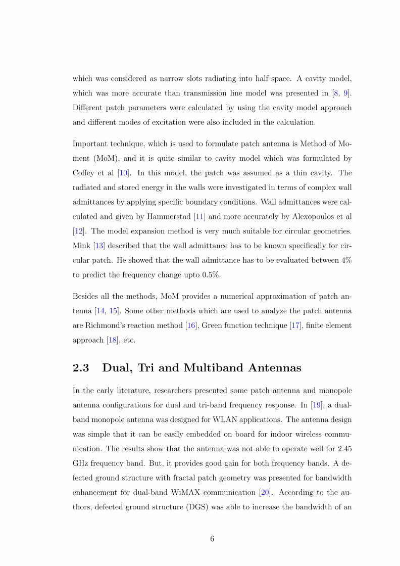
shaped monopole having two inverted L-shaped strips, shown in Fig 2.1, was pre-
sented in [23]. The presented antenna was able to provide resonance for 2.55 GHz,
3.5 GHz and 6.19 GHz frequency bands, respectively. Another planar monopole
antenna operating at GSM, DCS, WLAN and WiMAX applications was presented
in [24]. The authors used T-shaped radiator with a rectangular loop structure was
employed to achieve dual-band response. A G-shaped antenna was designed and
presented in [25]. By using a simple structure, a dual-band response for RFID
and WLAN applications was achieved. In [26], authors presented dual-band an-
tenna design for WLAN/WiMAX communications. They employed a key-like slot
in a rectangular patch to achieve dual-band response. It was also reported that
the presented antenna exhibited omni-directional radiation characteristics for both
frequency bands.
A compact CPW fed planar monopole antenna was presented for tri-band wireless
applications [27]. The authors utilized two inverted L-strips, a circular parasitic
element for tri-band characteristics. It was also described that the designed an-
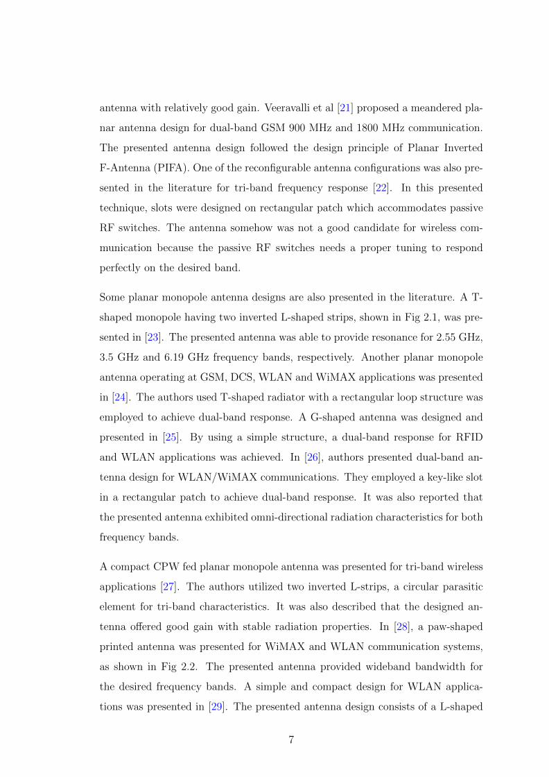
tenna offered good gain with stable radiation properties. In [28], a paw-shaped
printed antenna was presented for WiMAX and WLAN communication systems,
as shown in Fig 2.2. The presented antenna provided wideband bandwidth for
the desired frequency bands. A simple and compact design for WLAN applica-
tions was presented in [29]. The presented antenna design consists of a L-shaped
7
Progress In Electromagnetics Research C, Vol. 21, 2011 35
(a) (b)
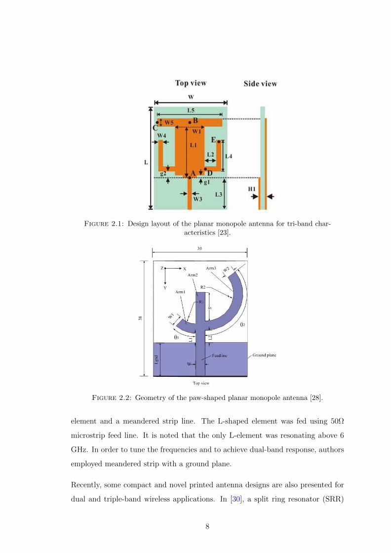
Figure 1. Geometry and photo of the proposed T-shaped monopoleantenna with a pair of mirrored L-shaped strips for multi-bandoperation. (a) Geometry. (b) Photo.
monopole patch is fed at point A and used to excite the fundamentaland second modes near 2.45/5.5GHz bands, respectively, in this study.And, the L-shaped monopole strip (L2+L4, from point D to point E)is inset at point D along the side edge of the T-shaped monopole patchto excite the fundamental mode close to 3.5GHz band. Compared withthe related T-shaped monopole antenna designs in the literature [16–19] only with dual-band (2.45/5GHz) operation by using dual- ortriple-T strips, this proposed triple-band monopole antenna providesvarious design criteria to support the worldwide interoperability formicrowave access (WiMAX) applications and achieve the multi-bandoperation to cover the 2.45/3.5/5.5GHzWLAN/WiMAX bands. First,for achieving the resonant mode at 2.45GHz band, the surface currentlength of the T-shaped patch (A → B → C) is chosen to be about34mm corresponding approximately to 0.28 and 0.59 wavelengths of2.45/5.5GHz bands. Detailed effects of the total length on the antennaperformances are analyzed with the aid of Table 2 and Figure 4 inSection 3. Also, the excited length (A → D → E) including the L-shaped strip (L2 + L4) is chosen to be about 28mm correspondingapproximately to 0.32 wavelength of 3.5GHz operation. The discussionof the antenna performances versus the L-shaped strip’s vertical length(L4) will be listed at Table 3 and shown in Figure 5. By properlyadjusting the width of the feeding microstrip line, good impedancematching across the operating band can easily be obtained.
Figure 2.1: Design layout of the planar monopole antenna for tri-band char-acteristics [23].Progress In Electromagnetics Research Letters, Vol. 23, 2011 149
Figure 1. Configuration of the presented antenna (Unit: mm).
As given by [18], for a dielectric substrate of thickness h,microstrip line width is w and relative permittivity εr, the effectivepermittivity is:
εre ≈1
2
[(εr + 1) + (εr − 1)
(1 +
12h
w
)]− 12
(4)
With εr = 4.4, h = 1.6mm and w = 3mm we can get εre = 3.3249.Then we can get the guided wavelength λg by the following
equation:
λg = λ0/√εre =
c0f√εre
(5)
The lengths of the three arms are set close to a quarter wave-length at2.4GHz, 3.4GHz, and 5.5GHz, respectively. So they can be calculatedby the equations above. The original widths of the three arms needsome fine tuning to get better impedance matching. Through thecommercial software High Frequency Structure Simulator (HFSS), allthe parameters are considered in the simulation. It is clear that every
Figure 2.2: Geometry of the paw-shaped planar monopole antenna [28].
element and a meandered strip line. The L-shaped element was fed using 50Ω
microstrip feed line. It is noted that the only L-element was resonating above 6
GHz. In order to tune the frequencies and to achieve dual-band response, authors
employed meandered strip with a ground plane.
Recently, some compact and novel printed antenna designs are also presented for
dual and triple-band wireless applications. In [30], a split ring resonator (SRR)
8
based monopole antenna was presented for dual-band wireless communications.
A compact U-slot based antenna was presented for tri-band wireless applications
[31]. According to the authors, it was the first antenna of its kind, whose size
was smaller than the antennas reported in literature. Another printed antenna
was presented in [32] for triple band characteristics. This antenna was smaller
than the antenna presented in [31]. The authors used crinkle structure to achieve
resonance at 1.78 GHz, 3.5 GHz and 5.26 GHz. Inspite of its small size, the
antenna offered good gain with a value of 2.7-dBi.
2.4 UWB Antennas with Extra Bands
In the 1980s, Federal Communication Commission (FCC) allocated Industrial Sci-
entific and Medicine (ISM) bands for unlicensed wideband communications. In
2002, the amendments were made in Part 15 by FCC, which directed unlicensed
radio devices to include the operation of UWB devices. For this purpose, a band-
width of 7.5 GHz was also allocated, i.e., 3.1-10.6 GHz. According to the FCC
rules, a signal having 500 MHz spectrum can be utilized in UWB systems. It
means that UWB is no more restricted to impulse radio. This increasing demand
in UWB systems stimulated researchers to design antennas for UWB communica-
tion systems.
For UWB systems, antenna designs faced many challenges, such as their impedance
bandwidth, radiation characteristics and electromagnetic interference (EMI) prob-
lems. With these challenges, the antenna design should be compact for easy inte-
gration in portable devices. On the other hand, now-a-days, the demand on single
antenna, which operates on multiple wireless frequency bands including UWB
band is increased. For this purpose, some of the antennas have been highlited in
the literature, which focused the integration of UWB frequency band with other
available wireless communication bands.
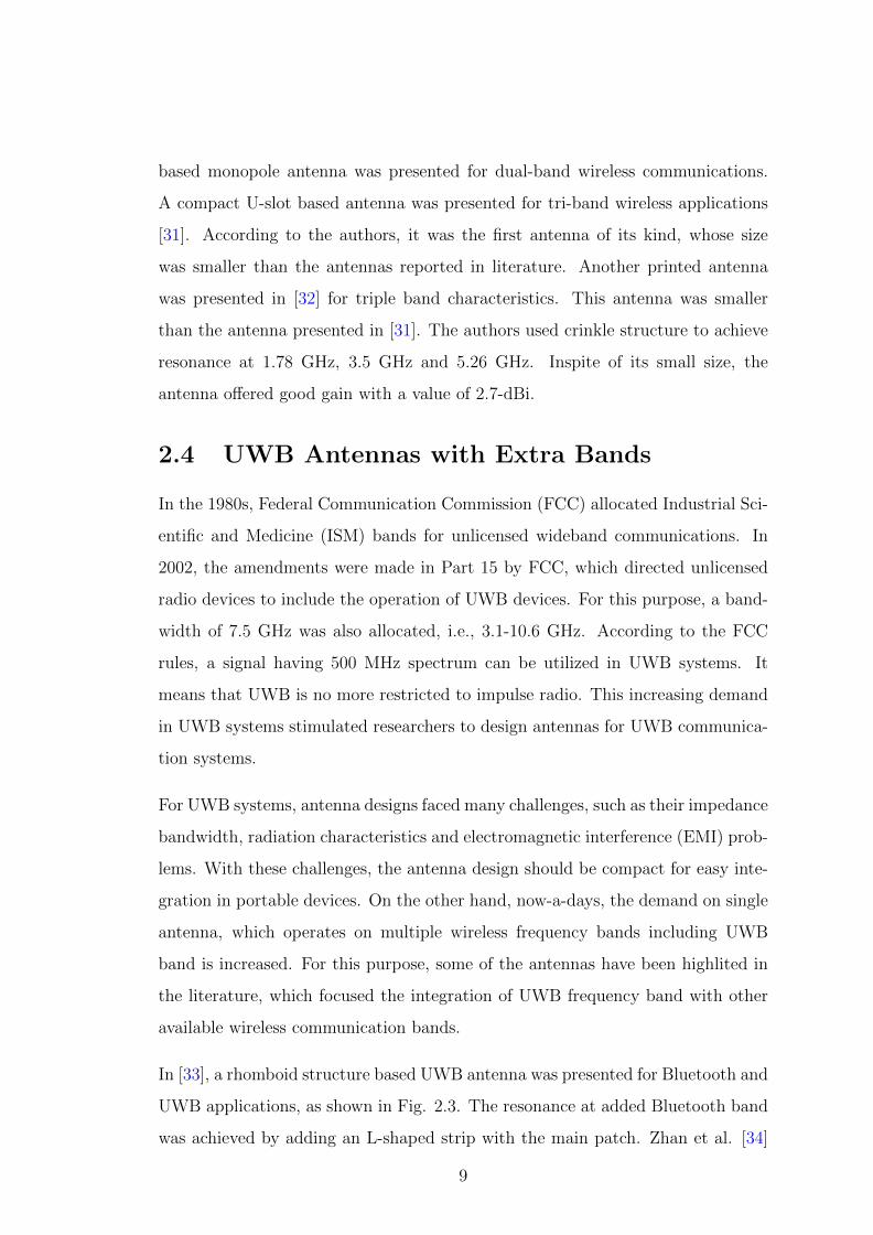
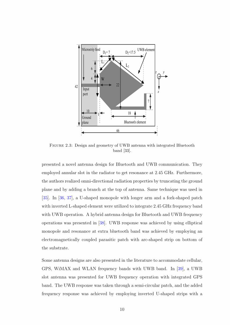
In [33], a rhomboid structure based UWB antenna was presented for Bluetooth and
UWB applications, as shown in Fig. 2.3. The resonance at added Bluetooth band
was achieved by adding an L-shaped strip with the main patch. Zhan et al. [34]
9
150 IEEE ANTENNAS AND WIRELESS PROPAGATION LETTERS, VOL. 8, 2009
Fig. 1. Microstrip-fed integrated Bluetooth/UWB antenna on a 42 46 mmFR-4 substrate (all dimensions are in millimeters).
A. Antenna Design
The design of the UWB rhomboid antenna starts withchoosing , , and . and are critical parametersassociated with the upper and lower operating frequencies of theantenna. , on the other hand, is a key parameter to maintain agood input impedance for the frequency range of 2.4–11 GHz.Accordingly, and are selected to have a reasonablereturn loss at GHz and GHz, whichare the lower and upper ends of the UWB band. A good startingpoint for these dimensions are as follows:
(1a)
(1b)
where is the effective wavelength for the radi-ation mode in the FR-4 substrate with the effective dielectricconstant ( for the 1-mm FR-4 substrate).and are the effective wavelengths at the upper and lowerUWB frequencies, respectively. is chosen to obtain reason-able return loss values for the whole frequency band. In partic-ular, the optimization of is critical for obtaining a good matchat the high end of the UWB spectrum. The L-shaped Bluetoothantenna element is strategically attached to the UWB antennaat one side at a position of minimum UWB current point to en-sure a minimal coupling between the two elements. This stripgenerates the 2.4–2.484 GHz Bluetooth band. The length ofthis strip is about a quarter-wave long at the operating frequency
GHz
(1c)
To better understand the behavior of the antenna, in partic-ular the interaction between Bluetooth and UWB resonances,the current distribution on the antenna has been studied.Fig. 2(b)–(d) show the current distribution at 2.45, 5, and10 GHz, respectively. As seen in Fig. 2(b), the resonant char-acter of the Bluetooth element appears highlighted at 2.45 GHz.The UWB element appears more active and the Bluetooth ele-ment appears colder at 5 GHz, as shown in Fig. 2(c). Finally.at 10 GHz, the lower part of the UWB element appearsactive with a clear null at the Bluetooth element connection.
Fig. 2. (a) Photograph of UWB/Bluetooth antenna, and the current distributionon the antenna at (b) 2.45, (c) 5, and (d) 10 GHz.
Fig. 3. Measured and simulated return losses of the antenna.
The current distribution results confirm that by locating theBluetooth element into a position of a minimum current, thegeneral behavior of the UWB antenna remains unchanged. It isalso worth noting that by separating the Bluetooth and UWBresonances, the unused spectrum between the two bands ismismatched at the antenna input. Hence, the issue of receiverdesensitization due to strong interferers that may exist withinthe unused spectrum may be reduced.
III. RESULTS AND DISCUSSIONS
Analysis of the integrated Bluetooth/UWB antenna is car-ried out using a full-wave EM analysis tool, HFSS_v11 by An-soft [5]. The return losses of the antenna for three variationsof the simulation model were compared with the measurementin Fig. 3. For the first simulation model, the conductive parts(antenna metallization, feed line, and ground plane) are mod-eled as single-sheet perfect electric conductor (PEC) referredto as the simple case. Two-faced solid conductors instead of asingle-sheet PEC are implemented for the second model. Thethird model has the two-faced solid conductors and takes intoaccount the SMA connector of the input port. Fig. 3 shows thatthe closest agreement between the return-loss simulations andthe measurement is achieved when the SMA connector is in-troduced in the simulated model. This shows that the feedingstructure plays a role in the behavior of this antenna. The centerfrequency of the Bluetooth band is excited at about 2.4 GHz,and the UWB spans the range of 3–12 GHz.
Antenna radiation pattern measurements have been per-formed in an anechoic chamber at 2.4, 5, and 10 GHz in
Figure 2.3: Design and geometry of UWB antenna with integrated Bluetoothband [33].
presented a novel antenna design for Bluetooth and UWB communication. They
employed annular slot in the radiator to get resonance at 2.45 GHz. Furthermore,
the authors realized omni-directional radiation properties by truncating the ground
plane and by adding a branch at the top of antenna. Same technique was used in
[35]. In [36, 37], a U-shaped monopole with longer arm and a fork-shaped patch
with inverted L-shaped element were utilized to integrate 2.45 GHz frequency band
with UWB operation. A hybrid antenna design for Bluetooth and UWB frequency
operations was presented in [38]. UWB response was achieved by using elliptical
monopole and resonance at extra bluetooth band was achieved by employing an
electromagnetically coupled parasitic patch with arc-shaped strip on bottom of
the substrate.
Some antenna designs are also presented in the literature to accommodate cellular,
GPS, WiMAX and WLAN frequency bands with UWB band. In [39], a UWB
slot antenna was presented for UWB frequency operation with integrated GPS
band. The UWB response was taken through a semi-circular patch, and the added
frequency response was achieved by employing inverted U-shaped strips with a
10
532 IEEE ANTENNAS AND WIRELESS PROPAGATION LETTERS, VOL. 11, 2012
Fig. 1. Antenna I: Configuration of the multiband printed UWB slot antennawith three inverted U-shaped strips. (a) Bottom layer. (b) Side view. (c) Toplayer. (d) Fabricated prototype.
Fig. 2. Configuration of the printed UWB antenna. (a) Antenna II: UWB baseantenna. (b) Antenna III: UWB antenna with three added strips in one side.
wavelength at the desired frequency. Thus, the length of eachstrip can be obtained approximately from the following formula:
(1)
in which , , and are dielectric constant, the velocity of lightin free space, and the center frequency of the desired band, re-spectively. To have a better impedance matching and a radiationpattern with lower cross polarization, the strips as obtained from(1) are also placed symmetrically on the other side of the patch.The shape of the final strips is in the form of an inverted U asshown in Fig. 1(a). This is referred to as Antenna I. Other pa-rameters of the UWB slot antenna with three inverted U-shaped
Fig. 3. Simulated reflection coefficient of Antenna I (UWB with three invertedU-shaped strips), Antenna II (UWB), and Antenna III (UWB with added stripsin one side). Measured reflection coefficient of Antenna I.
Fig. 4. Simulated reflection coefficient of Antenna I, with different configura-tions of U-shaped strips.
strips are optimized and are shown in Fig. 1(a) and (c). The fab-ricated prototype of the antenna is shown in Fig. 1(d).
III. RESULTS AND DISCUSSION
The reflection coefficient of the three types of antennasdiscussed in Section II—Antennas I, II, and III—is shown inFig. 3. Since the presence of the strips make the surface of theoctagonal slot smaller, the UWB starting frequency changes.As a result, the size of the base antenna without the strips(Antenna II) is set larger, effectively covering 2.3–11 GHz. Byadding three strips to the base antenna (Antenna III), the threeextra resonances would be created. To improve the impedancematching level of the three resonances, similar strips are placedsymmetrically on the other side of the patch (Antenna I). Ascan be seen from Fig. 3, the UWB printed slot antenna withthree inverted U-shape strips covers the whole of the UWBband (3.1–10.6 GHz) as well as the three extra linear polarizedbands [12].The measured reflection coefficients of the proposed UWB
printed slot antenna with the three inverted U-shaped stripsare also compared in Fig. 3. From the measured results, itcan be seen that the first band covers 1520–1590 MHz, the
Figure 2.4: Slot antenna configuration for multiband and UWB applications[40].
defected ground structure. It was also described that by changing the length of
the strips, one can optimize the design for other frequency bands. A novel and
compact UWB slot antenna design was presented with extra cellular and wireless
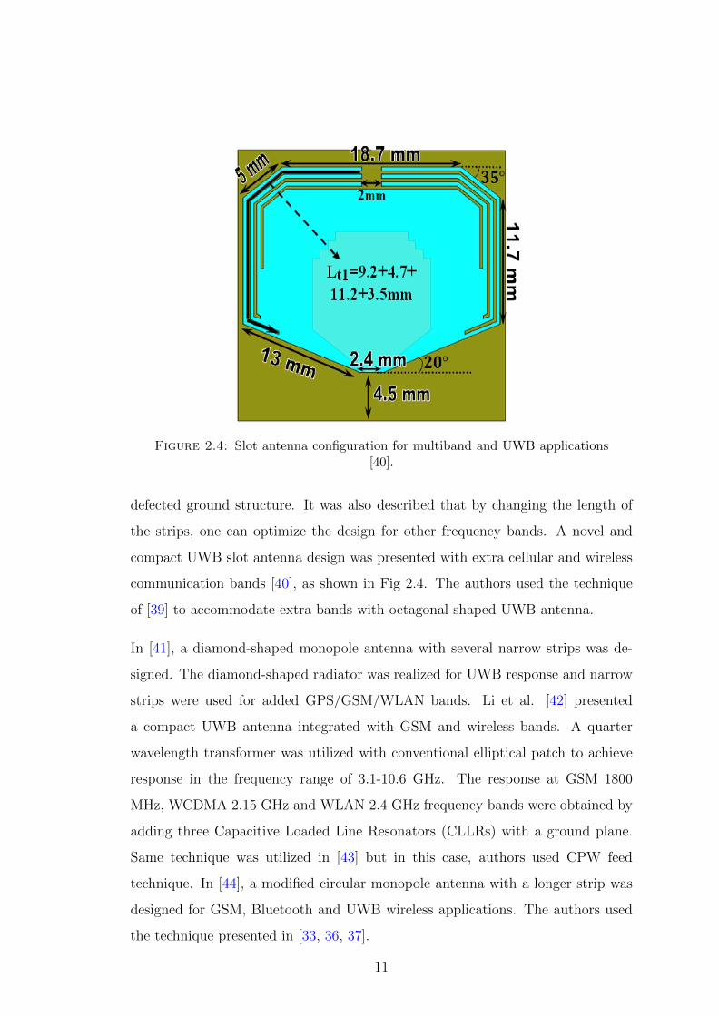
communication bands [40], as shown in Fig 2.4. The authors used the technique
of [39] to accommodate extra bands with octagonal shaped UWB antenna.
In [41], a diamond-shaped monopole antenna with several narrow strips was de-
signed. The diamond-shaped radiator was realized for UWB response and narrow
strips were used for added GPS/GSM/WLAN bands. Li et al. [42] presented
a compact UWB antenna integrated with GSM and wireless bands. A quarter
wavelength transformer was utilized with conventional elliptical patch to achieve
response in the frequency range of 3.1-10.6 GHz. The response at GSM 1800
MHz, WCDMA 2.15 GHz and WLAN 2.4 GHz frequency bands were obtained by
adding three Capacitive Loaded Line Resonators (CLLRs) with a ground plane.
Same technique was utilized in [43] but in this case, authors used CPW feed
technique. In [44], a modified circular monopole antenna with a longer strip was
designed for GSM, Bluetooth and UWB wireless applications. The authors used
the technique presented in [33, 36, 37].
11
2.5 Summary
In this chapter, we have briefly described the past work regarding the origin and
development of microstrip antennas. In the first part, basic printed antenna de-
signs are discussed, which were proposed by the researchers. The chapter has
discussed how antennas become an interesting field in wireless communication.
After that, different designs and configurations are discussed for dual-band, tri-
band and multiband antennas.
12
Chapter 3
MULTIBAND PLANAR MONOPOLE
ANTENNA
In this chapter, design of a printed antenna is presented for multiband cellular,
WiMAX and WLAN applications. The design procedure and results are also
discussed.
3.1 Proposed Antenna Design
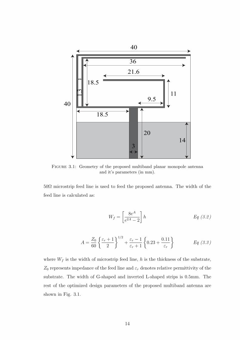
The design of the proposed planar multiband monopole antenna is shown in Fig.
3.1. The proposed antenna is designed on FR4 substrate with thickness, h = 1.6
mm and relative permittivity, εr = 4.4, respectively. It is shown in Fig. 3.1 that
the proposed antenna consists of a G-shaped and inverted L-shaped strips. Both
strips are connected to each other to realize multiband response. First of all, a G-
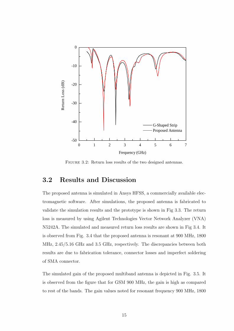
shaped radiator is designed and simulated in Ansys HFSS and its return loss result
is shown in Fig. 3.2. It is observed from the figure that the G-shaped radiator
is responsible to provide resonance at 1800 MHz, 2.45 GHz, 3.5 GHz and 5 GHz
frequency bands, respectively. After that, an inverted L-shaped strip is designed
with a G-shaped radiator to achieve resonance at 900 MHz and to shift 5 GHz
frequency band to the desired frequency, which is 5.25 GHz. The combined effect
of both the radiators is also provided in Fig 3.2. The length of both the radiators
is equal to λg/4, where λg is the guided wavelength and can be calculated as:
λg =c
fr√εeff
Eq (3.1 )
It is observed from the figure that the addition of inverted L-shaped strip shifts
5 GHz frequency band to 5.16 GHz and also provides resonance at 900 MHz.
Therefore, a final multiband antenna design is realized, as shown in Fig. 3.1. A
13
40
40
20
3
9.511
21.6
18.5
36
18.51.
3
14
Figure 3.1: Geometry of the proposed multiband planar monopole antennaand it’s parameters (in mm).
50Ω microstrip feed line is used to feed the proposed antenna. The width of the
feed line is calculated as:
Wf =
[8eA
e2A − 2
]h Eq (3.2 )
A =Z0
60
εr + 1
2
1/2
+εr − 1
εr + 1
0.23 +
0.11
εr
Eq (3.3 )
where Wf is the width of microstrip feed line, h is the thickness of the substrate,
Z0 represents impedance of the feed line and εr denotes relative permittivity of the
substrate. The width of G-shaped and inverted L-shaped strips is 0.5mm. The
rest of the optimized design parameters of the proposed multiband antenna are
shown in Fig. 3.1.
14
0 1 2 3 4 5 6 7- 5 0
- 4 0
- 3 0
- 2 0
- 1 0
0
Retur
n Loss
(dB)
F r e q u e n c y ( G H z )
G - S h a p e d S t r i p P r o p o s e d A n t e n n a
Figure 3.2: Return loss results of the two designed antennas.
3.2 Results and Discussion
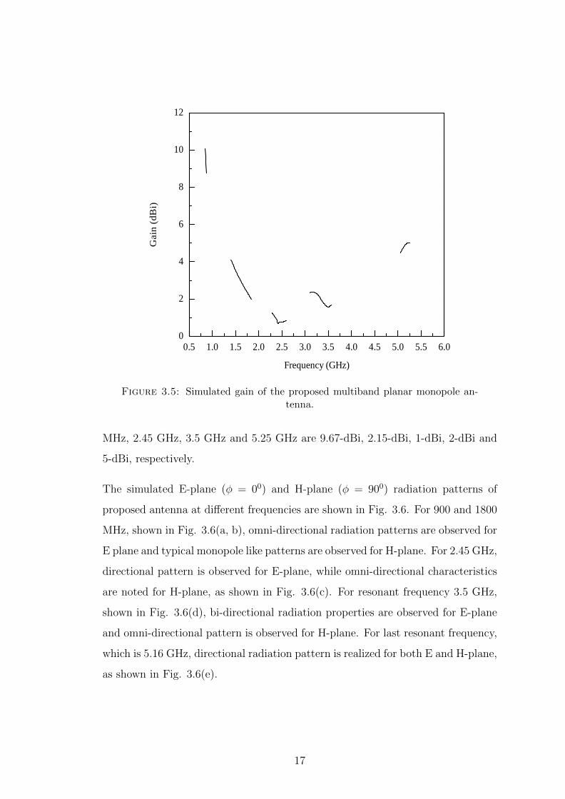
The proposed antenna is simulated in Ansys HFSS, a commercially available elec-
tromagnetic software. After simulations, the proposed antenna is fabricated to
validate the simulation results and the prototype is shown in Fig 3.3. The return
loss is measured by using Agilent Technologies Vector Network Analyzer (VNA)
N5242A. The simulated and measured return loss results are shown in Fig 3.4. It
is observed from Fig. 3.4 that the proposed antenna is resonant at 900 MHz, 1800
MHz, 2.45/5.16 GHz and 3.5 GHz, respectively. The discrepancies between both
results are due to fabrication tolerance, connector losses and imperfect soldering
of SMA connector.
The simulated gain of the proposed multiband antenna is depicted in Fig. 3.5. It
is observed from the figure that for GSM 900 MHz, the gain is high as compared
to rest of the bands. The gain values noted for resonant frequency 900 MHz, 1800
15
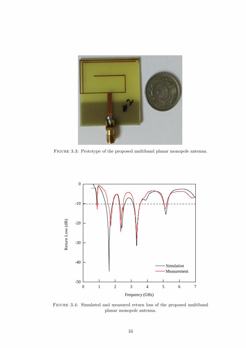
Figure 3.3: Prototype of the proposed multiband planar monopole antenna.
0 1 2 3 4 5 6 7- 5 0
- 4 0
- 3 0
- 2 0
- 1 0
0
Retur
n Loss
(dB)
F r e q u e n c y ( G H z )
S i m u l a t i o n M e a s u r e m e n t
Figure 3.4: Simulated and measured return loss of the proposed multibandplanar monopole antenna.
16
0 . 5 1 . 0 1 . 5 2 . 0 2 . 5 3 . 0 3 . 5 4 . 0 4 . 5 5 . 0 5 . 5 6 . 00
2
4
6
8
1 0
1 2
Gain
(dBi)
F r e q u e n c y ( G H z )
Figure 3.5: Simulated gain of the proposed multiband planar monopole an-tenna.
MHz, 2.45 GHz, 3.5 GHz and 5.25 GHz are 9.67-dBi, 2.15-dBi, 1-dBi, 2-dBi and
5-dBi, respectively.
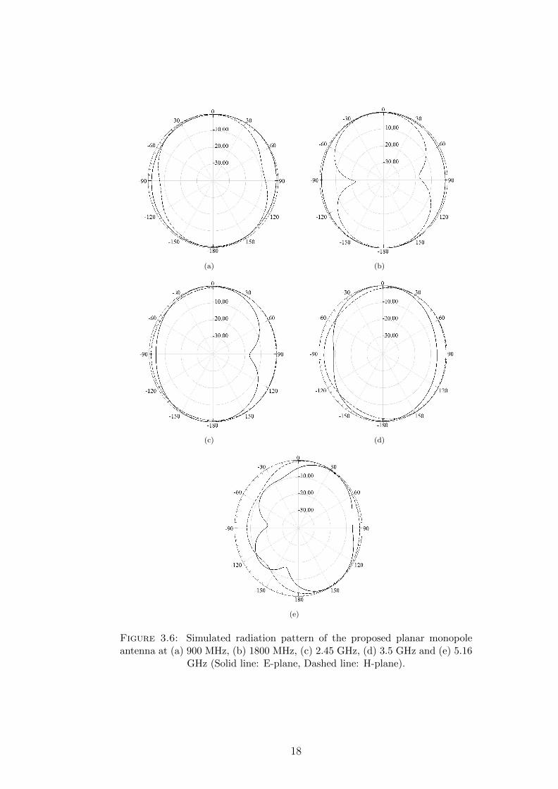
The simulated E-plane (φ = 00) and H-plane (φ = 900) radiation patterns of
proposed antenna at different frequencies are shown in Fig. 3.6. For 900 and 1800
MHz, shown in Fig. 3.6(a, b), omni-directional radiation patterns are observed for
E plane and typical monopole like patterns are observed for H-plane. For 2.45 GHz,
directional pattern is observed for E-plane, while omni-directional characteristics
are noted for H-plane, as shown in Fig. 3.6(c). For resonant frequency 3.5 GHz,
shown in Fig. 3.6(d), bi-directional radiation properties are observed for E-plane
and omni-directional pattern is observed for H-plane. For last resonant frequency,
which is 5.16 GHz, directional radiation pattern is realized for both E and H-plane,
as shown in Fig. 3.6(e).
17
(a) (b)
(c) (d)
(e)
Figure 3.6: Simulated radiation pattern of the proposed planar monopoleantenna at (a) 900 MHz, (b) 1800 MHz, (c) 2.45 GHz, (d) 3.5 GHz and (e) 5.16
GHz (Solid line: E-plane, Dashed line: H-plane).
18
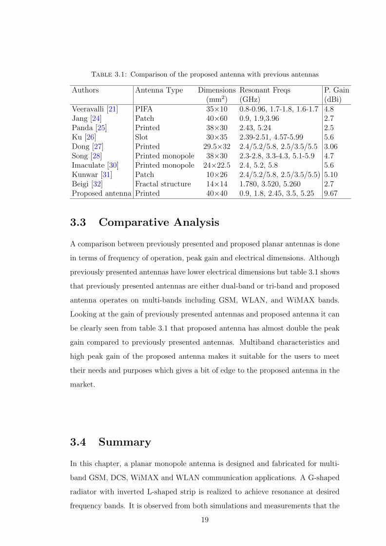
Table 3.1: Comparison of the proposed antenna with previous antennas
Authors Antenna Type Dimensions Resonant Freqs P. Gain(mm2) (GHz) (dBi)
Veeravalli [21] PIFA 35×10 0.8-0.96, 1.7-1.8, 1.6-1.7 4.8Jang [24] Patch 40×60 0.9, 1.9,3.96 2.7Panda [25] Printed 38×30 2.43, 5.24 2.5Ku [26] Slot 30×35 2.39-2.51, 4.57-5.99 5.6Dong [27] Printed 29.5×32 2.4/5.2/5.8, 2.5/3.5/5.5 3.06Song [28] Printed monopole 38×30 2.3-2.8, 3.3-4.3, 5.1-5.9 4.7Imaculate [30] Printed monopole 24×22.5 2.4, 5.2, 5.8 5.6Kunwar [31] Patch 10×26 2.4/5.2/5.8, 2.5/3.5/5.5) 5.10Beigi [32] Fractal structure 14×14 1.780, 3.520, 5.260 2.7Proposed antenna Printed 40×40 0.9, 1.8, 2.45, 3.5, 5.25 9.67
3.3 Comparative Analysis
A comparison between previously presented and proposed planar antennas is done
in terms of frequency of operation, peak gain and electrical dimensions. Although
previously presented antennas have lower electrical dimensions but table 3.1 shows
that previously presented antennas are either dual-band or tri-band and proposed
antenna operates on multi-bands including GSM, WLAN, and WiMAX bands.
Looking at the gain of previously presented antennas and proposed antenna it can
be clearly seen from table 3.1 that proposed antenna has almost double the peak
gain compared to previously presented antennas. Multiband characteristics and
high peak gain of the proposed antenna makes it suitable for the users to meet
their needs and purposes which gives a bit of edge to the proposed antenna in the
market.
3.4 Summary
In this chapter, a planar monopole antenna is designed and fabricated for multi-
band GSM, DCS, WiMAX and WLAN communication applications. A G-shaped
radiator with inverted L-shaped strip is realized to achieve resonance at desired
frequency bands. It is observed from both simulations and measurements that the
19
proposed monopole antenna is resonating at 900 MHz, 1800 MHz, 2.45 GHz, 3.5
GHz and 5.16 GHz, respectively. It is also observed that the proposed antenna
design exhibits good radiation properties and provides gain averaged 3.964 dBi on
desired frequencies and having peak gain at 9.67 dBi. A table is drawn at the end
to compare previously presented planar antennas and proposed antenna.
20
Chapter 4
PLANAR ANTENNA FOR CELLULAR AND
ULTRA-WIDEBAND COMMUNICATIONS
This chapter presents the design of a planar monopole antenna for cellular and
ultra-wideband (UWB) communications systems. The overall design process and
results are also discussed in this chapter.
4.1 Antenna Design
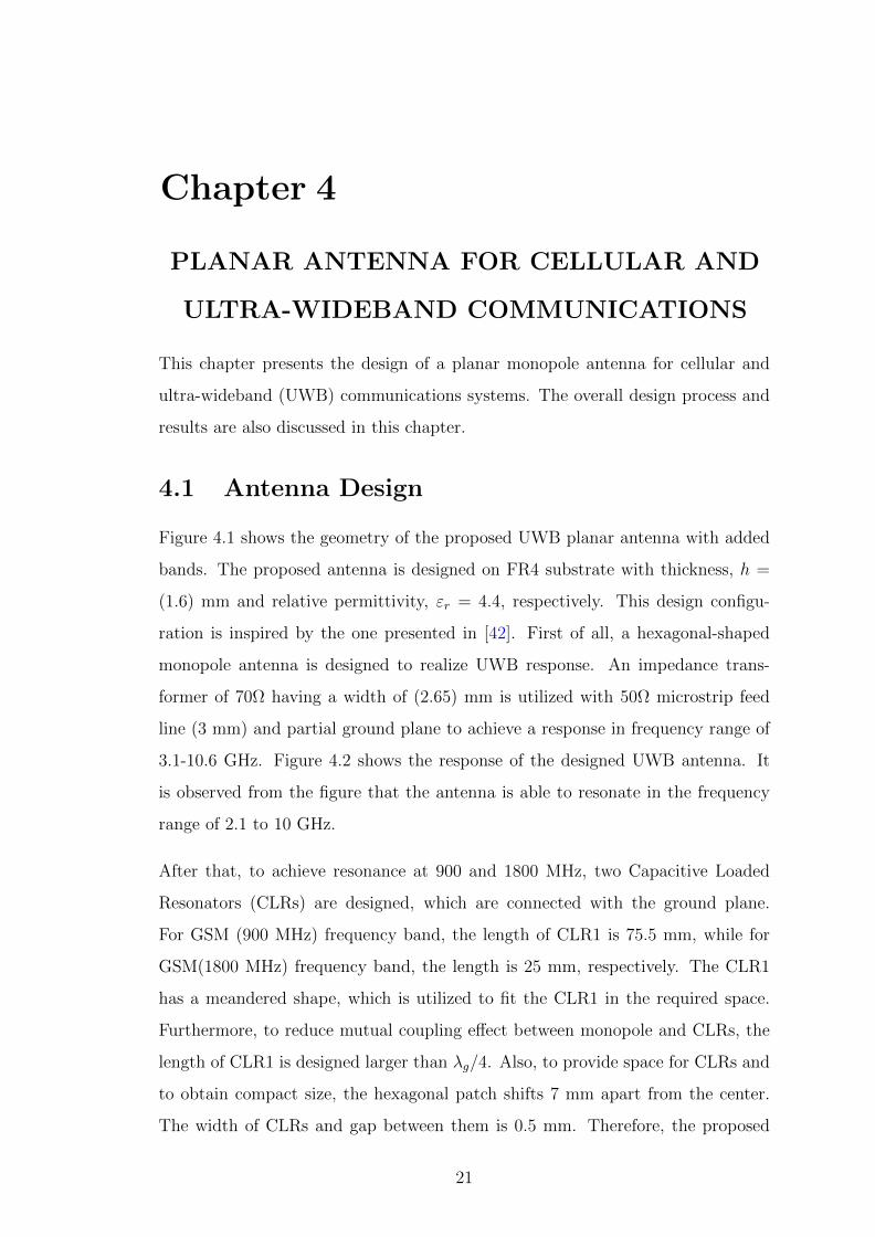
Figure 4.1 shows the geometry of the proposed UWB planar antenna with added
bands. The proposed antenna is designed on FR4 substrate with thickness, h =
(1.6) mm and relative permittivity, εr = 4.4, respectively. This design configu-
ration is inspired by the one presented in [42]. First of all, a hexagonal-shaped
monopole antenna is designed to realize UWB response. An impedance trans-
former of 70Ω having a width of (2.65) mm is utilized with 50Ω microstrip feed
line (3 mm) and partial ground plane to achieve a response in frequency range of
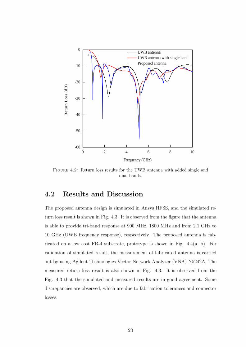
3.1-10.6 GHz. Figure 4.2 shows the response of the designed UWB antenna. It
is observed from the figure that the antenna is able to resonate in the frequency
range of 2.1 to 10 GHz.
After that, to achieve resonance at 900 and 1800 MHz, two Capacitive Loaded
Resonators (CLRs) are designed, which are connected with the ground plane.
For GSM (900 MHz) frequency band, the length of CLR1 is 75.5 mm, while for
GSM(1800 MHz) frequency band, the length is 25 mm, respectively. The CLR1
has a meandered shape, which is utilized to fit the CLR1 in the required space.
Furthermore, to reduce mutual coupling effect between monopole and CLRs, the
length of CLR1 is designed larger than λg/4. Also, to provide space for CLRs and
to obtain compact size, the hexagonal patch shifts 7 mm apart from the center.
The width of CLRs and gap between them is 0.5 mm. Therefore, the proposed
21
L
W
CLR1
CLR2
G
W1
W2
L1
LS
Lt
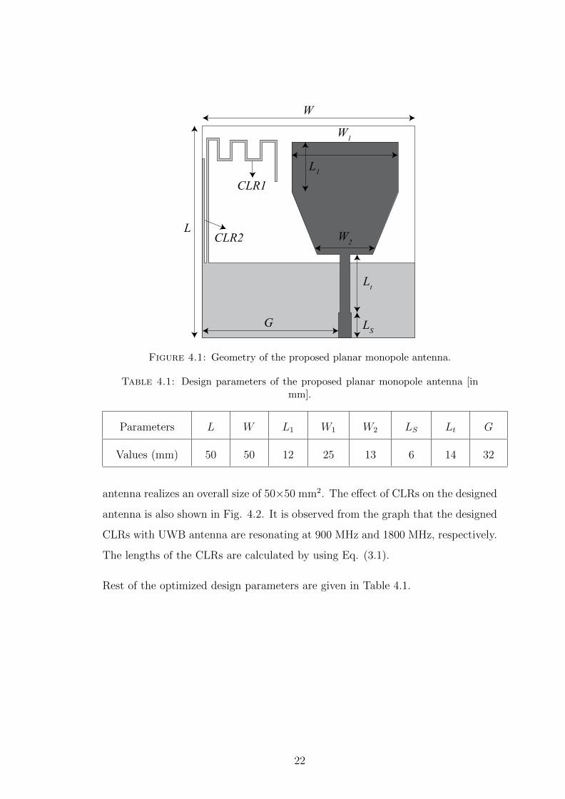
Figure 4.1: Geometry of the proposed planar monopole antenna.
Table 4.1: Design parameters of the proposed planar monopole antenna [inmm].
Parameters L W L1 W1 W2 LS Lt G
Values (mm) 50 50 12 25 13 6 14 32
antenna realizes an overall size of 50×50 mm2. The effect of CLRs on the designed
antenna is also shown in Fig. 4.2. It is observed from the graph that the designed
CLRs with UWB antenna are resonating at 900 MHz and 1800 MHz, respectively.
The lengths of the CLRs are calculated by using Eq. (3.1).
Rest of the optimized design parameters are given in Table 4.1.
22
U W B a n t e n n a U W B a n t e n n a w i t h s i n g l e b a n d P r o p o s e d a n t e n n a
0 2 4 6 8 1 0- 6 0
- 5 0
- 4 0
- 3 0
- 2 0
- 1 0
0
Retur
n Loss
(dB)
F r e q u e n c y ( G H z )Figure 4.2: Return loss results for the UWB antenna with added single and
dual-bands.
4.2 Results and Discussion
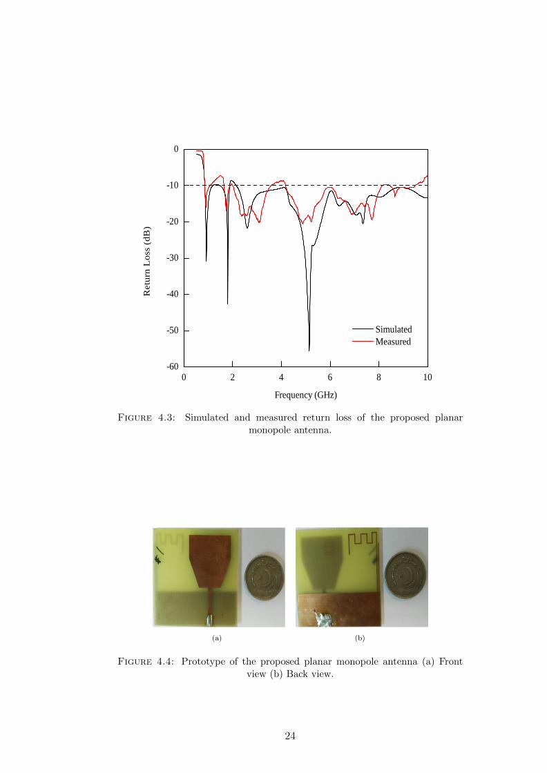
The proposed antenna design is simulated in Ansys HFSS, and the simulated re-
turn loss result is shown in Fig. 4.3. It is observed from the figure that the antenna
is able to provide tri-band response at 900 MHz, 1800 MHz and from 2.1 GHz to
10 GHz (UWB frequency response), respectively. The proposed antenna is fab-
ricated on a low cost FR-4 substrate, prototype is shown in Fig. 4.4(a, b). For
validation of simulated result, the measurement of fabricated antenna is carried
out by using Agilent Technologies Vector Network Analyzer (VNA) N5242A. The
measured return loss result is also shown in Fig. 4.3. It is observed from the
Fig. 4.3 that the simulated and measured results are in good agreement. Some
discrepancies are observed, which are due to fabrication tolerances and connector
losses.
23
0 2 4 6 8 1 0- 6 0
- 5 0
- 4 0
- 3 0
- 2 0
- 1 0
0
Re
turn L
oss (d
B)
F r e q u e n c y ( G H z )
S i m u l a t e d M e a s u r e d
Figure 4.3: Simulated and measured return loss of the proposed planarmonopole antenna.
(a) (b)
Figure 4.4: Prototype of the proposed planar monopole antenna (a) Frontview (b) Back view.
24
(a) (b)
Figure 4.5: Surface current distribution at (a) 900 MHz (b) 1800 MHz.
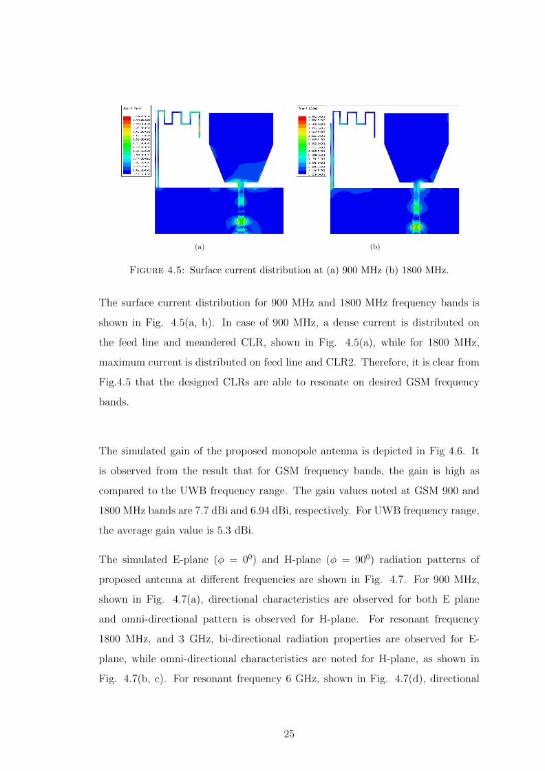
The surface current distribution for 900 MHz and 1800 MHz frequency bands is
shown in Fig. 4.5(a, b). In case of 900 MHz, a dense current is distributed on
the feed line and meandered CLR, shown in Fig. 4.5(a), while for 1800 MHz,
maximum current is distributed on feed line and CLR2. Therefore, it is clear from
Fig.4.5 that the designed CLRs are able to resonate on desired GSM frequency
bands.
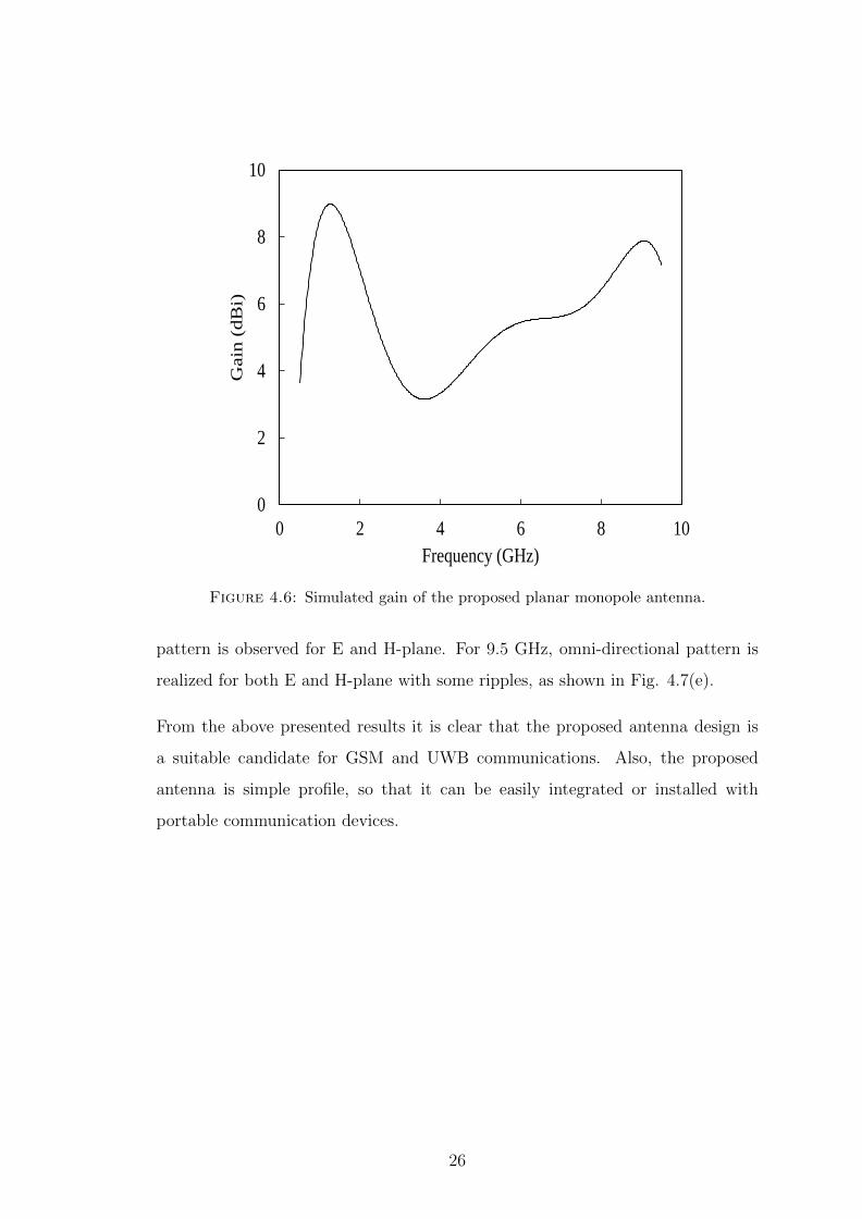
The simulated gain of the proposed monopole antenna is depicted in Fig 4.6. It
is observed from the result that for GSM frequency bands, the gain is high as
compared to the UWB frequency range. The gain values noted at GSM 900 and
1800 MHz bands are 7.7 dBi and 6.94 dBi, respectively. For UWB frequency range,
the average gain value is 5.3 dBi.
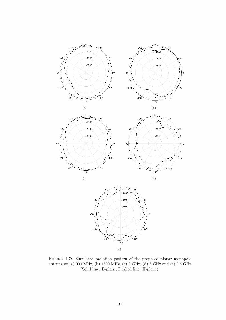
The simulated E-plane (φ = 00) and H-plane (φ = 900) radiation patterns of
proposed antenna at different frequencies are shown in Fig. 4.7. For 900 MHz,
shown in Fig. 4.7(a), directional characteristics are observed for both E plane
and omni-directional pattern is observed for H-plane. For resonant frequency
1800 MHz, and 3 GHz, bi-directional radiation properties are observed for E-
plane, while omni-directional characteristics are noted for H-plane, as shown in
Fig. 4.7(b, c). For resonant frequency 6 GHz, shown in Fig. 4.7(d), directional
25
0
2
4
6
8
10
0 2 4 6 8 10
Gain
(d
Bi)
Frequency (GHz)
Figure 4.6: Simulated gain of the proposed planar monopole antenna.
pattern is observed for E and H-plane. For 9.5 GHz, omni-directional pattern is
realized for both E and H-plane with some ripples, as shown in Fig. 4.7(e).
From the above presented results it is clear that the proposed antenna design is
a suitable candidate for GSM and UWB communications. Also, the proposed
antenna is simple profile, so that it can be easily integrated or installed with
portable communication devices.
26
(a) (b)
(c) (d)
(e)
Figure 4.7: Simulated radiation pattern of the proposed planar monopoleantenna at (a) 900 MHz, (b) 1800 MHz, (c) 3 GHz, (d) 6 GHz and (e) 9.5 GHz
(Solid line: E-plane, Dashed line: H-plane).
27
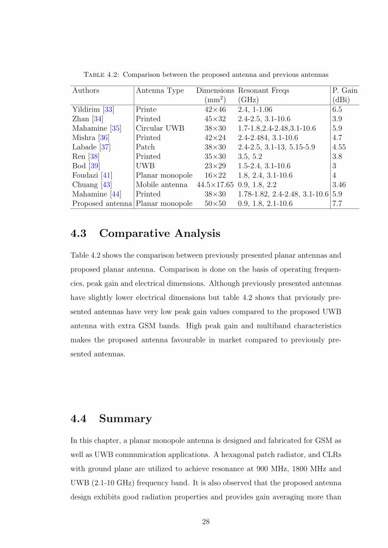
Table 4.2: Comparison between the proposed antenna and previous antennas
Authors Antenna Type Dimensions Resonant Freqs P. Gain(mm2) (GHz) (dBi)
Yildirim [33] Printe 42×46 2.4, 1-1.06 6.5Zhan [34] Printed 45×32 2.4-2.5, 3.1-10.6 3.9Mahamine [35] Circular UWB 38×30 1.7-1.8,2.4-2.48,3.1-10.6 5.9Mishra [36] Printed 42×24 2.4-2.484, 3.1-10.6 4.7Labade [37] Patch 38×30 2.4-2.5, 3.1-13, 5.15-5.9 4.55Ren [38] Printed 35×30 3.5, 5.2 3.8Bod [39] UWB 23×29 1.5-2.4, 3.1-10.6 3Foudazi [41] Planar monopole 16×22 1.8, 2.4, 3.1-10.6 4Chuang [43] Mobile antenna 44.5×17.65 0.9, 1.8, 2.2 3.46Mahamine [44] Printed 38×30 1.78-1.82, 2.4-2.48, 3.1-10.6 5.9Proposed antenna Planar monopole 50×50 0.9, 1.8, 2.1-10.6 7.7
4.3 Comparative Analysis
Table 4.2 shows the comparison between previously presented planar antennas and
proposed planar antenna. Comparison is done on the basis of operating frequen-
cies, peak gain and electrical dimensions. Although previously presented antennas
have slightly lower electrical dimensions but table 4.2 shows that prviously pre-
sented antennas have very low peak gain values compared to the proposed UWB
antenna with extra GSM bands. High peak gain and multiband characteristics
makes the proposed antenna favourable in market compared to previously pre-
sented antennas.
4.4 Summary
In this chapter, a planar monopole antenna is designed and fabricated for GSM as
well as UWB communication applications. A hexagonal patch radiator, and CLRs
with ground plane are utilized to achieve resonance at 900 MHz, 1800 MHz and
UWB (2.1-10 GHz) frequency band. It is also observed that the proposed antenna
design exhibits good radiation properties and provides gain averaging more than
28

5dBi. At the end of the chapter a comparison table is drawn which shows the peak
gain of the proposed antenna is 7.7dBi.
29
Chapter 5
CONCLUSION AND FUTURE WORK
5.1 Conclusion
With the rapid advancements in wireless communication systems, a number of
multiband antennas have been proposed. Selection of an appropriate antenna
is a crucial task in order to meet the stringent performance requirements of a
particular application. Owing to this, planar antennas remained a research subject
for considerable period of time because they have some advantages such as, low
cost, light weight and easy integration with hand-held devices.
In the first part of this thesis, a compact planar antenna is designed and presented
for multiband cellular and wireless communication systems. The proposed antenna
design consists of a G-shaped and inverted L-shaped strips, which are connected
to a 50Ω microstrip feed line. It is observed from both simulated and measured
results that the proposed monopole antenna is able to provide resonance at 900
MHz, 1800 MHz, 2.45 GHz, 3.5 GHz and 5.3 GHz frequency bands. Furthermore,
the designed antenna provides good gain and stable radiation properties for desired
bands. As well as, the antenna occupies an overall size of 40×40 mm2 so that it
can easily be integrated with hand-held devices.
In the second part of this thesis, a printed antenna is designed for ultra-wideband
(UWB) communication with added GSM frequency bands. The hexagonal-shaped
radiator with a quarter wavelength transformer is realized to achieve UWB fre-
quency range. The resonance at GSM frequency bands is achieved by adding
Capacitive Loaded Resonators (CLRs) with a partial ground plane. The simula-
tion results show that the proposed antenna is resonating at 900 MHz, 1800 MHz
and in the UWB range (2.1-10 GHz). The proposed antenna is fabricated to vali-
date the simulated data, and good agreement is observed between simulated and
30
measured results. Furthermore, the designed antenna provides good gain at GSM
frequency bands than UWB frequency band.
5.2 Future work
Based on the conclusion drawn above and the limitations of the presented work,
future work can be carried out in the following area:
1. For mobile and other compact portable devices, the size of an antenna should
be small. Therefore, future research should focus on further size reduction
of antennas by finding out new methods.
2. MIMO and massive MIMO communication systems have gained a lot of at-
tention to provide enhanced channel capacity and high data rate. Therefore,
an array of antennas with reduced mutual coupling can be developed.
3. It is observed the the proposed antenna designs are not properly providing
omni-directional radiation properties. So, a solution can be proposed to
overcome this problem.
31
REFERENCES
[1] E. Byron, “A new flush mounted antenna element for phased array applica-
tion,” Phased array antennas, pp. 187–192, 1972.
[2] J. Howell, “Microstrip antennas,” IEEE Transactions on Antennas and Prop-
agation, vol. 23, no. 1, pp. 90–93, 1975.
[3] H. Weinschel, “Progress report on development of microstrip cylindrical ar-
rays for sounding rockets,” Physic. and Sci. Lab., New Mexico State Univ.,
Las Cruces, 1973.
[4] G. Sanford, “Conformal microstrip phased array for aircraft tests with ATS-
6,” IEEE Transactions on Antennas and Propagation, vol. 26, no. 5, pp.
642–646, 1978.
[5] J. James and G. Wilson, “New design techniques for microstrip antenna ar-
rays,” in 5th European Microwave Conference, 1975, pp. 102–106.
[6] C. Garvin, R. Munson, L. Ostwald, and K. Schroeder, “Low profile, elec-
trically small missile base mounted microstrip antennas,” in Antennas and
Propagation Society International Symposium, vol. 13, 1975, pp. 244–247.
[7] A. Derneryd, “Linearly polarized microstrip antennas,” IEEE Transactions
on Antennas and Propagation, vol. 24, no. 6, pp. 846–851, 1976.
[8] Y. Lo, D. Solomon, and W. Richards, “Theory and experiment on microstrip
antennas,” IEEE Transactions on Antennas and Propagation, vol. 27, no. 2,
pp. 137–145, 1979.
[9] W. Richards, Y. Lo, and D. Harrison, “Improved theory for microstrip an-
tennas,” Electronics Letters, vol. 15, no. 2, pp. 42–44, 1979.
[10] E. Coffey and T. Lehman, “A new analysis technique for calculating the self
and mutual impedance of microstrip antennas,” in Proc. Workshop on Printed
Circuit Antennas, New Mexico State University, 1979, pp. 31–1.
32
[11] E. O. Hammerstad, “Equations for microstrip circuit design,” in 5th European
Microwave Conference, 1975, pp. 268–272.
[12] N. Alexopoulos and I. Rana, “Mutual impedance computation between
printed dipoles,” IEEE Transactions on Antennas and Propagation, vol. 29,
no. 1, pp. 106–111, 1981.
[13] J. Mink, “Sensitivity of microstrip antennas to admittance boundary varia-
tions,” IEEE Transactions on Antennas and Propagation, vol. 29, no. 1, pp.
142–144, 1981.
[14] C. A. Balanis, Antenna theory: analysis and design. John Wiley & Sons,
2016.
[15] E. Newman, “Strip antennas in a dielectric slab,” IEEE Transactions on
Antennas and Propagation, vol. 26, no. 5, pp. 647–653, 1978.
[16] J. Richmond, “A wire-grid model for scattering by conducting bodies,” IEEE
Transactions on Antennas and Propagation, vol. 14, no. 6, pp. 782–786, 1966.
[17] N. Alexopoulos, N. Uzunoglu, and I. Rana, “Radiation by microstrip
patches,” in Antennas and Propagation Society International Symposium,
vol. 17, 1979, pp. 722–727.
[18] K. R. Carver and E. L. Coffey, “Theoretical investigation of the microstrip
antenna.” New Mexico State Univ Las Cruces Physical Science Lab, Tech.
Rep., 1979.
[19] M. R. Khan, M. M. Morsy, M. Z. Khan, and F. J. Harackiewicz, “Dual band
antenna for wireless network (WLAN) applications,” in 2011 IEEE Inter-
national Symposium on Antennas and Propagation (APSURSI), 2011, pp.
1397–1400.
[20] V. Vaid and S. Agrawal, “Bandwidth optimization using fractal geometry on
rectangular microstrip patch antenna with DGS for wireless applications,” in
2014 International Conference on Medical Imaging, m-Health and Emerging
Communication Systems (MedCom), 2014, pp. 162–167.
33
[21] S. K. Veeravalli, K. Shambavi, and Z. C. Alex, “Design of multi band an-
tenna for mobile handset,” in 2013 IEEE Conference on Information and
Communication Technologies (ICT), 2013, pp. 949–952.
[22] M. Ali, N. Ramli, M. Salleh, and M. M. Tan, “A design of reconfigurable rect-
angular microstrip slot patch antennas,” in 2011 IEEE International Confer-
ence on System Engineering and Technology (ICSET), 2011, pp. 111–115.
[23] J.-H. Lu and Y.-H. Li, “Planar multi-band T-shaped monopole antenna with
a pair of mirrored L-shaped strips for WLAN/WiMAX operation,” Progress
In Electromagnetics Research C, vol. 21, pp. 33–44, 2011.
[24] J. Jang, S. Lee, and N. Kim, “Design of the dual-band planar monopole an-
tenna for coupled rectangular-loop structure and T-shape rectangular patch,”
in Progress In Electromagnetics Research Symposium, 2012, pp. 92–92.
[25] J. R. Panda, A. S. R. Saladi, and R. S. Kshetrimayum, “A compact printed
monopole antenna for dual-band RFID and WLAN applications,” Radioengi-
neering, vol. 20, no. 2, pp. 464–467, 2011.
[26] C.-H. Ku, H.-W. Liu, D.-Y. Lin, and Y.-X. Ding, “Compact dual-band
monopole antenna for WLAN/WiMAX applications,” in Progress in Elec-
tromagnetics Research Symposium, 2011, pp. 835–839.
[27] L. Dong, Z.-Y. Zhang, W. Li, and G. Fu, “A compact CPW-fed monopole
antenna with triple bands for WLAN/WiMAX applications,” Progress In
Electromagnetics Research Letters, vol. 39, pp. 103–113, 2013.
[28] Z.-N. Song, Y. Ding, and K. Huang, “A compact multiband monopole an-
tenna for WLAN/WiMAX applications,” Progress In Electromagnetics Re-
search Letters, vol. 23, pp. 147–155, 2011.
[29] X. Sun, S. Cheung, and T. Yuk, “A compact monopole antenna for WLAN
applications,” Microwave and Optical Technology Letters, vol. 56, no. 2, pp.
469–475, 2014.
34
[30] S. Imaculate Rosaline and S. Raghavan, “Metamaterial inspired monopole an-
tenna for WLAN/WiMAX applications,” Microwave and Optical Technology
Letters, vol. 58, no. 4, pp. 936–939, 2016.
[31] A. Kunwar, A. K. Gautam, and K. Rambabu, “Design of a compact U-
shaped slot triple band antenna for WLAN/WiMAX applications,” AEU-
International Journal of Electronics and Communications, vol. 71, pp. 82–88,
2017.
[32] P. Beigi and P. Mohammadi, “A novel small triple-band monopole antenna
with crinkle fractal-structure,” AEU-International Journal of Electronics and
Communications, vol. 70, no. 10, pp. 1382–1387, 2017.
[33] B. S. Yildirim, B. A. Cetiner, G. Roqueta, and L. Jofre, “Integrated bluetooth
and UWB antenna,” IEEE Antennas and Wireless Propagation Letters, vol. 8,
pp. 149–152, 2009.
[34] K. Zhan, Q. Quo, and K. Huang, “A novel kind of bluetooth and UWB
antenna,” in 2010 International Conference on Microwave and Millimeter
Wave Technology (ICMMT), 2010, pp. 1038–1041.
[35] S. D. Mahamine, R. S. Parbat, S. H. Bodake, and M. P. Aher, “Design of Blue-
tooth integrated UWB printed monopole antenna for wireless application,” in
International Conference on Automatic Control and Dynamic Optimization
Techniques (ICACDOT), 2016, pp. 1146–1151.
[36] S. K. Mishra, R. K. Gupta, A. Vaidya, and J. Mukherjee, “A compact dual-
band fork-shaped monopole antenna for Bluetooth and UWB applications,”
IEEE Antennas and Wireless Propagation Letters, vol. 10, pp. 627–630, 2011.
[37] R. Labade, S. Deosarkar, N. Pisharoty, and A. Malhotra, “Compact integrated
bluetooth UWB bandnotch antenna for personal wireless communication,”
Microwave and Optical Technology Letters, vol. 58, no. 3, pp. 540–546, 2016.
35
[38] F.-C. Ren, F.-S. Zhang, J. H. Bao, Y.-C. Jiao, and L. Zhou, “Printed blue-
tooth and UWB antenna with dual band-notched functions,” Progress In
Electromagnetics Research Letters, vol. 26, pp. 39–48, 2011.
[39] M. Bod, H. Hassani, and M. S. Taheri, “Compact printed UWB antenna with
a tuneable extra band,” in 2011 Loughborough Antennas and Propagation
Conference (LAPC), 2011, pp. 1–3.
[40] ——, “Compact UWB printed slot antenna with extra Bluetooth, GSM, and
GPS bands,” IEEE Antennas and Wireless Propagation Letters, vol. 11, pp.
531–534, 2012.
[41] A. Foudazi, H. R. Hassani et al., “Small UWB planar monopole antenna
with added GPS/GSM/WLAN bands,” IEEE Transactions on Antennas and
Propagation, vol. 60, no. 6, pp. 2987–2992, 2012.
[42] G. Li, H. Zhai, T. Li, X. Y. Ma, and C.-H. Liang, “Design of a compact
UWB antenna integrated with GSM/WCDMA/WLAN bands,” Progress In
Electromagnetics Research, vol. 136, pp. 409–419, 2013.
[43] C.-S. Chuang, T.-T. Ku, and J.-H. Zeng, “A compact multiband planar an-
tenna for integrated mobile wireless radio access applications,” in Asia Pacific
Microwave Conference (APMC), 2014, pp. 315–317.
[44] S. Mahamine and R. Labade, “A design of integrated GSM and Bluetooth
ultra wide band printed monopole antenna (UWB) for wireless applications,”
in 2015 IEEE Bombay Section Symposium (IBSS), 2015, pp. 1–6.
36
Related Documents